JP2023010387A - Light emitting device, manufacturing method, and waveguide structure - Google Patents
Light emitting device, manufacturing method, and waveguide structureDownload PDFInfo
- Publication number
- JP2023010387A JP2023010387AJP2021114488AJP2021114488AJP2023010387AJP 2023010387 AJP2023010387 AJP 2023010387AJP 2021114488 AJP2021114488 AJP 2021114488AJP 2021114488 AJP2021114488 AJP 2021114488AJP 2023010387 AJP2023010387 AJP 2023010387A
- Authority
- JP
- Japan
- Prior art keywords
- light
- optical waveguide
- end surface
- angle
- emitting device
- Prior art date
- Legal status (The legal status is an assumption and is not a legal conclusion. Google has not performed a legal analysis and makes no representation as to the accuracy of the status listed.)
- Pending
Links
Images


Classifications
- G—PHYSICS
- G02—OPTICS
- G02B—OPTICAL ELEMENTS, SYSTEMS OR APPARATUS
- G02B6/00—Light guides; Structural details of arrangements comprising light guides and other optical elements, e.g. couplings
- G02B6/24—Coupling light guides
- G02B6/42—Coupling light guides with opto-electronic elements
- G02B6/4201—Packages, e.g. shape, construction, internal or external details
- G02B6/4204—Packages, e.g. shape, construction, internal or external details the coupling comprising intermediate optical elements, e.g. lenses, holograms
- G02B6/4207—Packages, e.g. shape, construction, internal or external details the coupling comprising intermediate optical elements, e.g. lenses, holograms with optical elements reducing the sensitivity to optical feedback
- G—PHYSICS
- G02—OPTICS
- G02B—OPTICAL ELEMENTS, SYSTEMS OR APPARATUS
- G02B6/00—Light guides; Structural details of arrangements comprising light guides and other optical elements, e.g. couplings
- G02B6/0001—Light guides; Structural details of arrangements comprising light guides and other optical elements, e.g. couplings specially adapted for lighting devices or systems
- G02B6/0011—Light guides; Structural details of arrangements comprising light guides and other optical elements, e.g. couplings specially adapted for lighting devices or systems the light guides being planar or of plate-like form
- G02B6/0081—Mechanical or electrical aspects of the light guide and light source in the lighting device peculiar to the adaptation to planar light guides, e.g. concerning packaging
- G02B6/0086—Positioning aspects
- G02B6/0088—Positioning aspects of the light guide or other optical sheets in the package
- G—PHYSICS
- G02—OPTICS
- G02B—OPTICAL ELEMENTS, SYSTEMS OR APPARATUS
- G02B6/00—Light guides; Structural details of arrangements comprising light guides and other optical elements, e.g. couplings
- G02B6/0001—Light guides; Structural details of arrangements comprising light guides and other optical elements, e.g. couplings specially adapted for lighting devices or systems
- G02B6/0011—Light guides; Structural details of arrangements comprising light guides and other optical elements, e.g. couplings specially adapted for lighting devices or systems the light guides being planar or of plate-like form
- G02B6/0081—Mechanical or electrical aspects of the light guide and light source in the lighting device peculiar to the adaptation to planar light guides, e.g. concerning packaging
- G02B6/0086—Positioning aspects
- G02B6/009—Positioning aspects of the light source in the package
- G—PHYSICS
- G02—OPTICS
- G02B—OPTICAL ELEMENTS, SYSTEMS OR APPARATUS
- G02B6/00—Light guides; Structural details of arrangements comprising light guides and other optical elements, e.g. couplings
- G02B6/0001—Light guides; Structural details of arrangements comprising light guides and other optical elements, e.g. couplings specially adapted for lighting devices or systems
- G02B6/0011—Light guides; Structural details of arrangements comprising light guides and other optical elements, e.g. couplings specially adapted for lighting devices or systems the light guides being planar or of plate-like form
- G02B6/0081—Mechanical or electrical aspects of the light guide and light source in the lighting device peculiar to the adaptation to planar light guides, e.g. concerning packaging
- G02B6/0086—Positioning aspects
- G02B6/0091—Positioning aspects of the light source relative to the light guide
- G—PHYSICS
- G02—OPTICS
- G02F—OPTICAL DEVICES OR ARRANGEMENTS FOR THE CONTROL OF LIGHT BY MODIFICATION OF THE OPTICAL PROPERTIES OF THE MEDIA OF THE ELEMENTS INVOLVED THEREIN; NON-LINEAR OPTICS; FREQUENCY-CHANGING OF LIGHT; OPTICAL LOGIC ELEMENTS; OPTICAL ANALOGUE/DIGITAL CONVERTERS
- G02F1/00—Devices or arrangements for the control of the intensity, colour, phase, polarisation or direction of light arriving from an independent light source, e.g. switching, gating or modulating; Non-linear optics
- G02F1/35—Non-linear optics
- G02F1/37—Non-linear optics for second-harmonic generation
- G02F1/377—Non-linear optics for second-harmonic generation in an optical waveguide structure
- G—PHYSICS
- G02—OPTICS
- G02B—OPTICAL ELEMENTS, SYSTEMS OR APPARATUS
- G02B6/00—Light guides; Structural details of arrangements comprising light guides and other optical elements, e.g. couplings
- G02B6/24—Coupling light guides
- G02B6/26—Optical coupling means
- G02B6/32—Optical coupling means having lens focusing means positioned between opposed fibre ends
- G02B6/327—Optical coupling means having lens focusing means positioned between opposed fibre ends with angled interfaces to reduce reflections
- G—PHYSICS
- G02—OPTICS
- G02B—OPTICAL ELEMENTS, SYSTEMS OR APPARATUS
- G02B6/00—Light guides; Structural details of arrangements comprising light guides and other optical elements, e.g. couplings
- G02B6/24—Coupling light guides
- G02B6/42—Coupling light guides with opto-electronic elements
- G02B6/4201—Packages, e.g. shape, construction, internal or external details
- G02B6/4202—Packages, e.g. shape, construction, internal or external details for coupling an active element with fibres without intermediate optical elements, e.g. fibres with plane ends, fibres with shaped ends, bundles
- G02B6/4203—Optical features
- G—PHYSICS
- G02—OPTICS
- G02B—OPTICAL ELEMENTS, SYSTEMS OR APPARATUS
- G02B6/00—Light guides; Structural details of arrangements comprising light guides and other optical elements, e.g. couplings
- G02B6/24—Coupling light guides
- G02B6/42—Coupling light guides with opto-electronic elements
- G02B6/4201—Packages, e.g. shape, construction, internal or external details
- G02B6/4204—Packages, e.g. shape, construction, internal or external details the coupling comprising intermediate optical elements, e.g. lenses, holograms
- G02B6/4206—Optical features
Landscapes
- Physics & Mathematics (AREA)
- General Physics & Mathematics (AREA)
- Optics & Photonics (AREA)
- Nonlinear Science (AREA)
- Optical Couplings Of Light Guides (AREA)
- Optical Integrated Circuits (AREA)
- Optical Modulation, Optical Deflection, Nonlinear Optics, Optical Demodulation, Optical Logic Elements (AREA)
- Engineering & Computer Science (AREA)
- Manufacturing & Machinery (AREA)
Abstract
Translated fromJapanese
Description
Translated fromJapanese本開示は、一般に、発光装置、発光装置の製造方法、及び導波構造体に関する。本開示は、より詳細には、指向性を有する光を出射する光源と導波構造体とを備える発光装置、この発光装置の製造方法、及びこの発光装置に用いられる導波構造体に関する。 The present disclosure relates generally to light emitting devices, methods of manufacturing light emitting devices, and waveguide structures. More specifically, the present disclosure relates to a light-emitting device including a light source that emits light having directivity and a waveguide structure, a method for manufacturing the light-emitting device, and a waveguide structure used in the light-emitting device.
特許文献1は、発光装置として、光導波路型SHG素子を開示する。特許文献1では、半導体レーザから出射されるレーザ光の光軸に対して、光導波路型SHG素子の入射端面と出射端面の少なくとも一方がレーザ光の光軸に垂直な面に対して傾斜している。この構造により、入射端面または出射端面からの反射光がレーザ光源に戻りレーザ光源が損傷を受けるのを防止している。
しかし、特許文献1の発光装置では、レーザ光が光導波路内に効率よく入射し、レーザ光が光導波路内を伝搬中に外装部へ漏れ出さずに高効率で伝搬する構造については考慮されていない。また、光導波路内を伝搬するレーザ光の波長変換の効率についても考慮されておらず、波長変換効率が低くなるおそれがある。 However, in the light-emitting device of
本開示は、光源の損傷を低減でき、さらに光の利用効率及び波長変換効率の向上が図れる発光装置、製造方法、及び導波構造体を提供する。 The present disclosure provides a light-emitting device, a manufacturing method, and a waveguide structure that can reduce damage to the light source and improve the light utilization efficiency and wavelength conversion efficiency.
本開示の一態様の発光装置は、指向性を有する光を出射する光源と、入射端面及び出射端面を有し入射端面から入射した光を光の波長を変換して出射端面から出射する光導波路、及び光透過性を有し入射端面及び出射端面が露出するように光導波路を覆う外装部を含む導波構造体とを備える。光導波路の長さ方向は、光導波路の長さ方向及び光の光軸を含む所定面内において光の光軸に対して所定角度で傾斜する。所定角度は、光が光導波路内を光導波路と外装部との境界面で全反射しながら伝播するように設定される。 A light emitting device according to one aspect of the present disclosure includes a light source that emits light having directivity, and an optical waveguide that has an incident end surface and an emitting end surface and converts the wavelength of light incident from the incident end surface and emits the light from the emitting end surface. , and a waveguide structure including an exterior part having optical transparency and covering the optical waveguide so that the incident end face and the exit end face are exposed. The length direction of the optical waveguide is inclined at a predetermined angle with respect to the optical axis of light within a predetermined plane including the length direction of the optical waveguide and the optical axis of light. The predetermined angle is set so that the light propagates through the optical waveguide while being totally reflected at the interface between the optical waveguide and the exterior.
本開示の一態様の製造方法は、指向性を有する光を出射する光源と、入射端面及び出射端面を有し入射端面から入射した光を光の波長を変換して出射端面から出射する光導波路、及び光透過性を有し入射端面及び出射端面が露出するように光導波路を覆う外装部を含む導波構造体とを備える発光装置の製造方法である。前記製造方法は、所定角度を、光が光導波路内を光導波路と外装部との界面で全反射しながら伝播するように設定することを含む。所定角度は、光導波路の長さ方向及び光の光軸を含む所定面内における光導波路の長さ方向と光の光軸との間の角度である。 A manufacturing method according to one aspect of the present disclosure includes a light source that emits light having directivity, and an optical waveguide that has an incident end surface and an emitting end surface and converts the wavelength of light incident from the incident end surface and emits the light from the emitting end surface. , and a waveguide structure including a light-transmissive exterior covering the optical waveguide so that the incident end face and the exit end face are exposed. The manufacturing method includes setting the predetermined angle so that the light propagates in the optical waveguide while being totally reflected at the interface between the optical waveguide and the exterior. The predetermined angle is the angle between the length direction of the optical waveguide and the optical axis of light in a predetermined plane containing the length direction of the optical waveguide and the optical axis of light.
本開示の一態様の導波構造体は、入射端面及び出射端面を有し入射端面から入射した指向性を有する光を光の波長を変換して出射端面から出射する光導波路と、光透過性を有し入射端面及び出射端面が露出するように光導波路を覆う外装部とを備える。光導波路の長さ方向は、光導波路の長さ方向及び光の光軸を含む所定面内において光の光軸に対して所定角度で傾斜する。所定角度は、光が光導波路内を光導波路と外装部との界面で全反射しながら伝播するように設定される。 A waveguide structure according to one aspect of the present disclosure includes an optical waveguide that has an incident facet and an emitting facet and that converts the wavelength of light having directivity incident from the incident facet and emits the light from the emitting facet; and an exterior covering the optical waveguide so that the incident end surface and the output end surface are exposed. The length direction of the optical waveguide is inclined at a predetermined angle with respect to the optical axis of light within a predetermined plane including the length direction of the optical waveguide and the optical axis of light. The predetermined angle is set so that the light propagates through the optical waveguide while being totally reflected at the interface between the optical waveguide and the exterior.
本開示の態様によれば、光源の損傷を低減でき、さらに光の利用効率及び波長変換効率の向上が図れる。 According to the aspect of the present disclosure, it is possible to reduce damage to the light source, and further improve the light utilization efficiency and the wavelength conversion efficiency.
以下、適宜図面を参照しながら、実施の形態を詳細に説明する。但し、必要以上に詳細な説明は省略する場合がある。例えば、既によく知られた事項の詳細説明や実質的に同一の構成に対する重複説明を省略する場合がある。これは、以下の説明が不必要に冗長になるのを避け、当業者の理解を容易にするためである。なお、発明者(ら)は、当業者が本開示を十分に理解するために添付図面および以下の説明を提供するのであって、これらによって特許請求の範囲に記載の主題を限定することを意図するものではない。 Hereinafter, embodiments will be described in detail with reference to the drawings as appropriate. However, more detailed description than necessary may be omitted. For example, detailed descriptions of well-known matters and redundant descriptions of substantially the same configurations may be omitted. This is to avoid unnecessary verbosity in the following description and to facilitate understanding by those skilled in the art. It is noted that the inventor(s) provide the accompanying drawings and the following description in order for those skilled in the art to fully understand the present disclosure, which are intended to limit the claimed subject matter. not something to do.
[1.実施の形態]
[1.1 実施の形態1]
[1.1.1 概要]
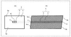
図1は、実施の形態1の発光装置1の構成例の概略側面図である。図1の発光装置1は、光源2と、導波構造体5とを備える。光源2は、指向性を有する光6を出射する。導波構造体5は、光導波路3と、外装部4とを備える。光導波路3は、入射端面7及び出射端面8を有し、入射端面7から入射した光6を光の波長を変換して出射端面8から出射する。外装部4は、光透過性を有し、入射端面7及び出射端面8が露出するように光導波路3を覆う。光導波路3の長さ方向Aは、光導波路3の長さ方向A及び光6の光軸11を含む所定面内において光6の光軸11に対して所定角度で傾斜する。所定角度は、光6が光導波路3内を光導波路3と外装部4との界面Bで全反射しながら伝播するように設定される。[1. Embodiment]
[1.1 Embodiment 1]
[1.1.1 Overview]
FIG. 1 is a schematic side view of a configuration example of a
図1の発光装置1では、光導波路3の長さ方向Aが、光導波路3の長さ方向A及び光6の光軸11を含む所定面内において光6の光軸11に対して所定角度で傾斜する。そのため、光6の進行方向が、光導波路3の長さ方向に対して傾斜する。これにより、光6が光導波路3と外装部4との境界面Bで反射しながら光導波路3内を伝搬する光路長が、光導波路3の長さよりも長くなるため、波長変換の効率が高くなる。図1の発光装置1では、所定角度は、光6が光導波路3内を光導波路3と外装部4との界面Bで全反射しながら伝播するように設定される。これにより、光6は光導波路3から外装部4へ漏れ出さずにより効率良く伝搬することが可能である。したがって、本実施の形態の発光装置1によれば、光源の損傷を低減でき、さらに光の利用効率及び波長変換効率の向上が図れる。 In the
[1.1.2 詳細]
以下、本実施の形態の発光装置1について詳細に説明する。図1に示すように、発光装置1は、光源2と、導波構造体5とを備える。[1.1.2 Details]
The light-
光源2は、指向性を有する光6を出射する。図1では、光6は、光軸11に沿って進行する。光源2は、レーザ、例えば、半導体レーザである。光6は、レーザ光である。光源2は、例えば、活性層2aを有する。光源2の活性層2aの一端面が、光6が出射する出射面2bとなる。なお、半導体レーザは、加工用レーザ等に比べて低出力であるが小型であるため、小型の光学系と組み合わせることで小型の発光装置を構成することができる。光6の波長は、可視光領域の波長に限定されず、赤外線領域の波長及び紫外領域の波長であってもよい。 The
図2は、導波構造体5の構成例を示す。図2において、(a)は導波構造体5の正面図であり、(b)は導波構造体5の断面図である。導波構造体5は、光導波路3と、外装部4とを備える。 FIG. 2 shows a configuration example of the
光導波路3は、光源2から出射された光6の伝送路である。光導波路3は、入射端面7と出射端面8とを有する。光導波路3は、入射端面7から入射した光6を光6の波長を変換して出射端面8から出射する。 The
図1に示すように、導波構造体5において、光導波路3の長さ方向Aは、光導波路3の長さ方向A及び光6の光軸11を含む所定面内において光6の光軸11に対して所定角度(第1所定角度)(図1においてθ1で示す)で傾斜する。θ1は、光導波路3の長さ方向Aに対して図1の時計周りの方向を正とする。また、導波構造体5において、入射端面7は、所定面内において光導波路3の長さ方向Aに垂直な垂直面Pに対して第2所定角度(図1においてθ2で示す)で傾斜する。θ2は、垂直面Pに対して図1の時計周りの方向を正とする。さらに、導波構造体5において、出射端面8は、所定面内において垂直面Pに対して第3所定角度(図1においてθ3で示す)で傾斜する。θ3は、垂直面Pに対して図1の時計周りの方向を正とする。第1所定角度θ1~第3所定角度θ3については後述する。As shown in FIG. 1, in the
本実施の形態では、光導波路3は六面体状である。より詳細には、本実施形態では、光導波路3の長さ方向Aの両面である入射端面7及び出射端面8は長方形であり、厚み方向の両面(図2(b)における上面及び下面)は長方形であり、幅方向の両面(図2(a)における左面及び右面)は台形である。光導波路3の形状はこれに限定されず、光6を伝送可能な形状であればよい。光導波路3は、光を透過する性質を有する材料、例えば、石英ガラス、サファイアなどの酸化物材料、シリコン、窒化ガリウムや窒化アルミニウムをはじめとする半導体等の無機材料、又はポリイミド系樹脂、ポリアミド系樹脂等のポリマー材料により形成される。 In this embodiment, the
外装部4は、光導波路3を覆う。図2の外装部4は、光導波路3の入射端面7及び出射端面8が露出するように光導波路3を覆う。外装部4は、直方体状である。外装部4は、外装部4の長さ方向が光導波路3の長さ方向Aに一致するように、光導波路3を覆う。光導波路3の入射端面7及び出射端面8は、外装部4の長さ方向の第1及び第2面4a,4bにそれぞれ露出する。本実施の形態では、外装部4は、光透過性を有する。外装部4は、光を透過する性質を有する材料、例えば、石英ガラス、サファイアなどの酸化物材料、シリコン、窒化ガリウムや窒化アルミニウムをはじめとする半導体等の無機材料、又はポリイミド系樹脂、ポリアミド系樹脂等のポリマー材料により形成される。本実施の形態において、外装部4は、光導波路3よりも屈折率が小さい材料により形成される。 The
導波構造体5は、例えば、光導波路型SHG素子である。図2の導波構造体5は、光源2側の端面5aと、光源2とは反対側の端面5bとを有する。端面5aは、光導波路3の入射端面7と外装部4の第1面4aとを含む。端面5bは、光導波路3の出射端面8と外装部4の第2面4bとを含む。導波構造体5の光導波路3の入射端面7から光導波路3に入射した光6は、光導波路3と外装部4との界面Bで反射しながら光導波路3の長さ方向Aに伝搬し、伝搬の過程で波長が変換される。波長が変換された光6は、出射端面8から導波構造体5の外部に出射される。 The
本実施の形態では、光6は指向性を有しており、例えば、レーザ光である。レーザ光は、一般に直進性が良いとされるが、実際には一定の角度に拡大しながら進む場合が多い。光源2から出射した光6が光導波路3の外側まで拡大した場合には、光6の一部が光導波路3に入らず損失となり、光結合の効率が低下する。そこで、発光装置1は、光6を収束させるために収束光学系20をさらに備える。 In this embodiment, the
収束光学系20は、光源2と導波構造体5との間に配置される。収束光学系20は、光6の光軸11上にあって光6を入射端面7に収束させる。図1の収束光学系20は、第1凸レンズ9と、第2凸レンズ10とを備える。収束光学系20は、最も入射端面7側に位置する部品(第2凸レンズ10)が収束レンズであるように構成されている。第1凸レンズ9と、第2凸レンズ10とは、光6の光軸11上にあって、光源2からの光6は第1凸レンズ9、第2凸レンズ10をこの順番に通過して、導波構造体5に入射する。光6は第1凸レンズ9によって平行光となり、第2凸レンズ10によって収束される。このように、収束光学系20では、光源2と導波構造体5との間に配置された第1凸レンズ9と第2凸レンズ10とを用いて、光6を収束させる。本実施の形態では、光6はレーザ光である。一般にレーザ光の強度分布はガウシアン分布である。図2(a)において、領域Rは、導波構造体5の端面5aに入射する光6のピーク強度の1/e2で規定されるビーム断面に対応する。収束光学系20によって、図2(a)に示すように、領域Rは、入射端面7内に収まる。つまり、領域Rは、端面5aにおいて入射端面7内にあり、第1面4aには位置していない。換言すれば、光6の入射端面7における断面が、入射端面7に包含されているといえる。本実施の形態では、領域Rが入射端面7内に収まっているから、光6を光導波路3内に入射させる際の損失を低減させることができる。特に、図2(a)では、領域Rの形状は楕円形であり、光導波路3の入射端面7の形状は長方形である。ここで、領域Rの径は、入射端面7の短辺の長さより小さく、これにより、領域Rが入射端面7に包含されている。そのため、光6を効率よく光導波路3内に入射させることができる。Converging
上述したように、図1の発光装置1では、光導波路3の長さ方向Aは、光導波路3の長さ方向A及び光6の光軸11を含む所定面内において光6の光軸11に対して第1所定角度(図1においてθ1で示す)で傾斜する。これにより、光6が光導波路3と外装部4との境界面Bで反射しながら光導波路3内を伝搬する光路長が、光導波路3の長さよりも長くなるため、波長変換の効率が高くなる。また、図1の導波構造体5において、入射端面7は、所定面内において光導波路3の長さ方向Aに垂直な垂直面Pに対して第2所定角度(図1においてθ2で示す)で傾斜する。これによって、光導波路3への入射端面7において反射した光6の一部が収束光学系20を介して光源2に戻る可能性を低減できる。これにより、光6の戻り光で光源2が損傷してしまう可能性を低減できる。As described above, in the light-emitting
以下、第1所定角度θ1及び第2所定角度θ2の関係についてさらに説明する。The relationship between the first predetermined angle θ1 and the second predetermined angle θ2 will be further described below.
図1の発光装置1では、第1所定角度θ1及び第2所定角度θ2は、光6が光導波路3内を光導波路3と外装部4との境界面Bで全反射しながら伝播するように設定される。これにより、光6は光導波路3から外装部4へ漏れ出さずにより効率良く伝搬することが可能である。次に、図3を参照して、第1所定角度θ1及び第2所定角度θ2の関係について説明する。In the
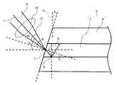
図3は、発光装置1の導波構造体5の入射端面7を説明する概略断面図である。なお、図3では、単に図面を見やすくするためだけに、断面を示すハッチングを省略している。 FIG. 3 is a schematic cross-sectional view for explaining the
図3において、入射端面7から光導波路3内に入射した光6が光導波路3外に漏れ出さずに効率的に伝搬していくには、光導波路3と外装部4との境界面Bで全反射して光導波路3の長さ方向Aに進むことが望ましい。本実施の形態では、光6は第2凸レンズ10により収束しながら入射端面7に入射するので、図3における光6の外縁21が、外装部4への入射角が最小となる。第1所定角度θ1及び第2所定角度θ2は、光6の光軸を通る中心光線ではなく光6のピーク強度の1/e2で規定されるビームの外縁21が光導波路3と外装部4との境界面Bで全反射する条件を満たすように、設定される。図3において、所定面内での光6の外縁21の入射端面7への入射角をθi、所定面内での収束光学系20により入射端面7に収束する光6の光束の頂角をφ1とする。頂角φ1は、入射端面7に入射する光6の光束の最も外側の光束間の角度である。この場合、θiは、θi=θ1+φ1/2-θ2で表わされる。外装部4の屈折率をn1、光導波路3の屈折率をn2、屈折角をθrとすると、スネルの法則より、sin(θi)/sin(θr)=n2/n1が成立する。そうすると、sin(θr)=sin(θ1+φ1/2-θ2)/n2であるから、θr=arcsin{sin(θ1+φ1/2-θ2)/n2}となる。光6の外縁21が光導波路3から外装部4に入射する入射角をθcとすると、θc=180°-90°-θr-θ2であるから、θc=90°-arcsin{sin(θ1+φ1/2-θ2)/n2}-θ2である。光6の外縁21が光導波路3と外装部4の境界面Bで全反射する条件は、θc≧arcsin(n1/n2)である。よって、90°-arcsin{sin(θ1+φ1/2-θ2)/n2}-θ2≧arcsin(n1/n2)との式をθ1について解くと、次式(1)が得られる。In FIG. 3, in order for the

以上から、本実施の形態の発光装置1では、外装部4の屈折率をn1、光導波路3の屈折率をn2、第1所定角度をθ1、第2所定角度をθ2、所定面内での収束光学系20により入射端面7に収束する光6の光束の頂角をφ1とすると、θ1は、上式(1)を満たす。As described above, in the light-emitting
図1の発光装置1では、第1所定角度θ1及び第2所定角度θ2は、光6のピーク強度の1/e2で規定されるビームが入射端面7で反射した一部が光源2に入射しないように設定される。これにより、光6の戻り光で光源2が損傷してしまうのを防ぐことができる。次に、図4を参照して、第1所定角度θ1及び第2所定角度θ2の関係について説明する。In the
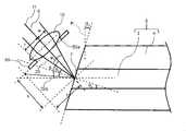
図4は、発光装置1の導波構造体5の光導波路3の入射端面7を説明する概略断面図である。なお、図4では、単に図面を見やすくするためだけに、断面を示すハッチングを省略している。 FIG. 4 is a schematic cross-sectional view for explaining the
図4において、光6のピーク強度の1/e2で規定されるビームの一部が入射端面7において反射して、入射端面7での反射光が第2凸レンズ10に戻ると、さらに第2凸レンズ10及び第1凸レンズ9を介して光源2まで戻り、反射光のエネルギーにより光源2が損傷してしまう可能性がある。これを防止するためには、入射端面7での反射光が第2凸レンズ10に戻るのを抑制することが考えられる。本実施の形態では、光6は第2凸レンズ10により収束しながら入射端面7に入射するので、図4における光6のピーク強度の1/e2で規定されるビームの外縁22が、入射端面7への入射角が最小となる。光6の外縁22が、入射端面7で反射後に第2凸レンズ10に戻らないという条件を満たすように、第1所定角度θ1及び第2所定角度θ2が設定される。図4において、所定面内での光6の外縁22の入射端面7への入射角をθk、所定面内での収束光学系20により入射端面7に収束する光6の光束の頂角をφ1とする。この場合、θk=θ1-φ1/2-θ2が成立する。光6の外縁22の入射端面7における反射光22aの反射角もθkである。入射端面7から収束光学系20までの距離をxとする。図4の場合、収束光学系20は、最も入射端面7側に位置する部品が収束レンズ(第2凸レンズ10)であるように構成されている。よって、xは、入射端面7から収束レンズ(第2凸レンズ10)までの距離である。より詳細には、xは、入射端面7から収束レンズ(第2凸レンズ10)の表面までの距離である。所定面内での光6の光軸11に直交する方向における、光軸11と反射光22aとの距離をyとする。この場合、yは、y=x・tan(2θk+φ1/2)で表される。θk=θ1-φ1/2-θ2であるから、y=x・tan(2θ1-2θ2-φ1/2)である。収束光学系20の有効半径をrとする。図4の場合、収束光学系20は、最も入射端面7側に位置する部品が収束レンズ(第2凸レンズ10)であるように構成されている。よって、rは、収束レンズ(第2凸レンズ10)の半径である。r<yであれば、光6の外縁22の反射光22aが第2凸レンズ10に入射しない。y=x・tan(2θ1-2θ2-φ1/2)であるから、r<x・tan(2θ1-2θ2-φ1/2)であり、これをθ1について解くと、次式(2)が得られる。In FIG. 4, a part of the beam defined by 1/e2 of the peak intensity of the

以上から、収束光学系20の有効半径をr、入射端面7から収束光学系20までの距離をx、第1所定角度をθ1、第2所定角度をθ2、所定面内での収束光学系20により入射端面7に収束する光6の光束の頂角をφ1とすると、θ1は、上式(2)を満たす。From the above, r is the effective radius of the converging
上述したように、図1の発光装置1では、導波構造体5において、出射端面8が所定面内において垂直面Pに対して第3所定角度θ3で傾斜する。第1所定角度θ1、第2所定角度θ2、及び第3所定角度θ3は、光導波路3内から出射端面8を通って外部に出ようとする光6が出射端面8で全反射されないように設定される。これにより、光6が光導波路3内に閉じ込められる可能性を低減して、光6の利用効率の向上が図れる。次に、図5を参照して、第1所定角度θ1、第2所定角度θ2、及び第3所定角度θ3の関係について説明する。As described above, in the
図5は、発光装置1の導波構造体5の光導波路3の出射端面8を説明する概略断面図である。なお、図5では、単に図面を見やすくするためだけに、断面を示すハッチングを省略している。 FIG. 5 is a schematic cross-sectional view for explaining the
図5において、光導波路3内を伝搬後に出射端面8から出射する光6の量を増やすためには、出射端面8において反射して光導波路3内に戻る光6の量を抑制することが考えられる。本実施の形態では、光導波路3内を伝搬する光6のうち光導波路3から外装部4への入射角が最小となる外縁23に関して、光導波路3から外装部4への入射角をθcとする。図3と同様に、θc=90°-arcsin{sin(θ1+φ1/2-θ2)/n2}-θ2である。光6の外縁23の、出射端面8への入射角をθsとする。θsは、θs=90°-(θc-θ3)で表される。光6の外縁23が、出射端面8で全反射せずに導波構造体5の外部に出射する条件は、θs<arcsin(1/n2)である。θs=90°-(θc-θ3)を代入すると、90°-θc+θ3<arcsin(1/n2)である。これをθ3について解くと、次式(3)が得られる。In FIG. 5, in order to increase the amount of

以上から、光導波路3の屈折率をn2、第1所定角度をθ1、第2所定角度をθ2、第3所定角度をθ3、所定面内での収束光学系20により入射端面7に収束する光6の光束の頂角をφ1とすると、θ3は、上式(3)を満たす。From the above, the refractive index of the
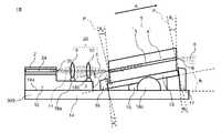
上述したように、発光装置1は、光源2と、導波構造体5と、収束光学系20とを備え、更に、光源2と導波構造体5と収束光学系20とを支持するサポート30を備える。本実施の形態では、光源2と、導波構造体5と、収束光学系20とはサポート30に取り付けられることで、互いに位置関係が規定される。 As described above, the light-emitting
図1のサポート30は、第1取付部材12と、第2取付部材13と、基体14と、高さ調整部材15と、第1位置決めガイド16と、第2位置決めガイド17とを備える。 The
第1取付部材12は、基体14の配置面14aに配置される。光源2及び収束光学系20は、第1取付部材12における基体14とは反対側の面(図1における上面)に設置される。第1取付部材12は熱伝導性が高い材料により形成されており、これによって、光源2の熱を基体14に伝達して放散させることができる。このように、第1取付部材12は、高さ調整機能と冷却機能とを有する。 The first mounting
第2取付部材13は、基体14の配置面14aに配置される。導波構造体5は、第2取付部材13における基体14とは反対側の面(図1における上面)に設置される。第2取付部材13は熱伝導性が高い材料により形成されており、これによって、導波構造体5の熱を基体14に伝達して放散させることができる。このように、第2取付部材13は、高さ調整機能と冷却機能とを有する。 The second mounting
高さ調整部材15は、基体14の配置面14aと第1取付部材12との間に配置される。高さ調整部材15は、基体14の配置面14aに対する第1取付部材12の高さを調整する機構であり、かつ、光6の光軸11を光導波路3の長さ方向Aに対して傾斜させて設置する機構である。高さ調整部材15の配置面14aとは反対側の面(図1における上面)は、基体14の配置面14aに対して、第1所定角度θ1で傾斜している。これにより、光源2から出射される光6の光軸11に対する光導波路3の長さ方向Aの角度もθ1となる。高さ調整部材15は、例えば、くさび形である。高さ調整部材15は、所定面内において光6の光軸11を光導波路3の長さ方向Aに対して第1所定角度θ1で傾斜させる角度調整部材である。The
第1位置決めガイド16及び第2位置決めガイド17は、高さ調整部材15とともに、所定面内における光6の光軸11と光導波路3の長さ方向Aとの間の角度を第1所定角度θ1に維持したまま光源2を移動させる位置調整部材を構成する。位置調整部材は、光源2を平行に移動させるための平行移動補助部材である。第1位置決めガイド16は、第1取付部材12の導波構造体5に対向する端面に設置される。第2位置決めガイド17は、第1取付部材12の導波構造体5とは反対側の端面に設置される。第1位置決めガイド16の第1取付部材12に接する面は、光導波路3の長さ方向Aに垂直な垂直面Pに対して第2所定角度θ2で傾斜している。同様に、第2位置決めガイド17の第1取付部材12に接する面も、光導波路3の長さ方向Aに垂直な垂直面Pに対して第2所定角度θ2で傾斜している。The
高さ調整部材15を基体14の配置面14aに沿って導波構造体5に近付く方向又は導波構造体5から離れる方向(光導波路3の長さ方向A)に移動させると、光源2が、所定面内における光6の光軸11と光導波路3の長さ方向Aとの間の角度が第1所定角度θ1に維持されたまま第1位置決めガイド16及び第2位置決めガイド17に沿って移動する。これにより、光源2の出射面2bと入射端面7との距離を保ったまま、すなわち、導波構造体5において光6が入射する領域Rの大きさを保ったまま、光源2の出射面2bを、所定面内における光6の光軸11と光導波路3の長さ方向Aとの間の角度を第1所定角度θ1に維持したまま移動させることができる。このため、入射端面7に光6が効率良く入射する位置の調整が容易になる。When the
収束光学系20の第1凸レンズ9及び第2凸レンズ10と、高さ調整部材15とは、導波構造体5により所定の波長に変換された光6の量が最大となるようにそれらの位置が調整された後に、接着剤18a,18b,18c等の固定手段で第1取付部材12及び基体14に固定される。図1では、第1凸レンズ9及び第2凸レンズ10が接着剤18a,18bにより第1取付部材12に固定され、高さ調整部材15が接着剤18cにより基体14に固定されている。接着剤18a,18b,18cは、接着対象の部材を接着位置に設置して塗布した後も即座に硬化せず、位置調整が可能なものである。接着剤18a,18b,18cは、例えば紫外線硬化樹脂である。 The first
次に、光源2と、収束光学系20と、導波構造体5とをサポート30に取り付ける方法について説明する。まず、導波構造体5を第2取付部材13に取り付ける。次に、第2取付部材13を基体14の配置面14aに設置し、固定する。光源2及び収束光学系20を第1取付部材12に取り付ける。この時点では、収束光学系20の第1凸レンズ9及び第2凸レンズ10は、未固定である。次に高さ調整部材15を基体14の配置面14aに設置する。第1取付部材12を高さ調整部材15に載置する。第1取付部材12及び高さ調整部材15は、未固定である。次に、接着剤18a,18b,18cとして紫外線硬化樹脂を塗布する。第1凸レンズ9、第2凸レンズ10、及び高さ調整部材15は、未固定である。この後に、基体14の配置面14aに第1位置決めガイド16及び第2位置決めガイド17を設置し、固定する。この後に、光源2に電気系統を接続して光源2から光6を出射させる。この状態で、入射端面7を含む平面内において光6が最も収束するように第1凸レンズ9と第2凸レンズ10の精密な位置調整を行う。その後、高さ調整部材15を導波構造体5に対して接近又は離間する方向(光導波路3の長さ方向A)に移動させ、出射端面8から出射する光6の量が最大となるように精密な位置調整を行う。つまり、光6が入射する領域Rが入射端面7内に収まるように、収束光学系20の調整を行う。位置調整の後、紫外線を照射して接着剤18a,18b,18cを硬化させ、第1凸レンズ9、第2凸レンズ10、第1取付部材12及び高さ調整部材15を固定する。これによって、図1に示す発光装置1が得られる。 Next, a method for attaching the
[1.1.3 効果等]
以上述べたように、発光装置1は、指向性を有する光6を出射する光源2と、入射端面7及び出射端面8を有し入射端面7から入射した光6を光6の波長を変換して出射端面8から出射する光導波路3、及び光透過性を有し入射端面7及び出射端面8が露出するように光導波路3を覆う外装部4を含む導波構造体5とを備える。光導波路3の長さ方向Aは、光導波路3の長さ方向A及び光6の光軸11を含む所定面内において光6の光軸11に対して所定角度で傾斜する。所定角度は、光6が光導波路3内を光導波路3と外装部4との境界面Bで全反射しながら伝播するように設定される。この構成によれば、光源2の損傷を低減でき、さらに光6の利用効率及び波長変換効率の向上が図れる。[1.1.3 Effects, etc.]
As described above, the
また、発光装置1において、導波構造体5の端面5aに入射する光6のピーク強度の1/e2で規定されるビーム断面に対応する領域Rは、入射端面7内に収まる。この構成によれば、光6の利用効率の向上が図れる。In the
また、発光装置1は、光6の光軸11上にあって光6を入射端面7に収束させる収束光学系20をさらに備える。この構成によれば、光6の利用効率及び波長変換効率の向上が図れる。 The
また、発光装置1において、外装部4の屈折率をn1、光導波路3の屈折率をn2、所定角度をθ1、所定面内において入射端面7と光導波路3の長さ方向Aに垂直な垂直面Pのなす角度をθ2、所定面内での収束光学系20により入射端面7に収束する光6の光束の頂角をφ1とすると、θ1は、
また、発光装置1において、所定角度は、光6のピーク強度の1/e2で規定されるビームの入射端面7で反射した一部が光源2に入射しないように設定される。この構成によれば、光源2の損傷の防止が図れる。In the
また、発光装置1において、収束光学系20の有効半径をr、入射端面7から収束光学系20までの距離をx、所定角度をθ1、所定面内において入射端面7と光導波路3の長さ方向Aに垂直な垂直面Pのなす角度をθ2、所定面内での収束光学系20により入射端面7に収束する光6の光束の頂角をφ1とすると、θ1は、
また、発光装置1において、収束光学系20は、最も入射端面7側に位置する部品が収束レンズ(第2凸レンズ10)であるように構成される。有効半径は、収束レンズの半径である。入射端面7から収束光学系20までの距離は、入射端面7から収束レンズまでの距離である。この構成によれば、光源2の損傷を低減できる。 Further, in the
また、発光装置1において、出射端面8は、所定面内において垂直面Pに対して傾斜する。この構成によれば、光6の利用効率の向上が図れる。 Further, in the
また、発光装置1において、光導波路3の屈折率をn2、所定角度をθ1、所定面内において入射端面7と光導波路3の長さ方向Aに垂直な垂直面Pのなす角度をθ2、所定面内において出射端面8が垂直面Pに対して傾斜する角度をθ3、所定面内での収束光学系20により入射端面7に収束する光6の光束の頂角をφ1とすると、θ3は、
また、発光装置1は、所定面内において光6の光軸11を光導波路3の長さ方向Aに対して所定角度で傾斜させる角度調整部材(高さ調整部材15)と、所定面内における光6の光軸11と光導波路3の長さ方向Aとの間の角度を所定角度に維持したまま光源2の出射面2bと入射端面7の距離を一定に保ちながら、光源2及び導波構造体5の少なくとも一方を移動させる位置調整部材(高さ調整部材15、第1及び第2位置決めガイド16,17)とをさらに備える。この構成によれば、光源2と導波構造体5との位置関係を容易に設定できる。 In addition, the
また、発光装置1は、光源2と導波構造体5とが配置される配置面14aを有する基体14をさらに備える。光源2の光6の光軸11が所定面内において基体14の配置面14aの沿面方向に対して傾斜する。この構成によれば、光源2と導波構造体5との位置関係を容易に設定できる。 The light-emitting
また、発光装置1において、導波構造体5は、光導波路型SHG素子である。この構成によれば、光6の波長変換効率の向上が図れる。 Further, in the
以上述べた発光装置1の製造方法は、所定角度を、光6が光導波路3内を光導波路3と外装部4との境界面Bで全反射しながら伝播するように設定することを含む。所定角度は、光導波路3の長さ方向A及び光6の光軸11を含む所定面内における光導波路3の長さ方向Aと光6の光軸11との間の角度である。この構成によれば、光6の利用効率及び波長変換効率の向上が図れる。 The manufacturing method of the
また、製造方法は、位置調整部材により光源2及び導波構造体5の少なくとも一方を移動させることによって導波構造体5の出射端面8から出射する光6の量が最大となるように光源2と導波構造体5の位置を決定することを含む。この構成によれば、光源2と導波構造体5との位置関係を容易に設定できる。 In addition, the manufacturing method is such that at least one of the
以上述べた導波構造体5は、入射端面7及び出射端面8を有し入射端面7から入射した指向性を有する光6を光6の波長を変換して出射端面8から出射する光導波路3と、光透過性を有し入射端面7及び出射端面8が露出するように光導波路3を覆う外装部4とを備える。光導波路3の長さ方向Aは、光導波路3の長さ方向A及び光6の光軸11を含む所定面内において光6の光軸11に対して所定角度で傾斜する。所定角度は、光6が光導波路3内を光導波路3と外装部4との境界面Bで全反射しながら伝播するように設定される。この構成によれば、光6の利用効率及び波長変換効率の向上が図れる。 The
[1.2 実施の形態2]
[1.2.1 構成]
図6は、実施の形態2の発光装置1Aの構成例の概略側面図である。図6の発光装置1Aは、実施の形態1の発光装置1と同様に、光源2と、導波構造体5とを備える。[1.2 Embodiment 2]
[1.2.1 Configuration]
FIG. 6 is a schematic side view of a configuration example of the
図6の発光装置1Aは、収束光学系20を備える代わりに、光源2と光導波路3との間に配置される反射防止膜40をさらに備える。反射防止膜40の厚み方向の第1面40aは光源2の出射面2bに接する。反射防止膜40の厚み方向の第2面40bは光導波路3の入射端面7に接する。これによって、光源2は、反射防止膜40を介して、導波構造体5と直接結合している。なお、本実施の形態において、反射防止膜40は均一な厚みを有している。そのため、所定面内において入射端面7と光導波路3の長さ方向Aに垂直な垂直面Pのなす角度(第2所定角度θ2)は、第1所定角度θ1に等しい。つまり、光源2の出射面2bと光導波路3の入射端面7とは互いに平行である。The light-emitting
図6の反射防止膜40は、光6を透過する。本実施の形態では、光6はレンズ等の収束光学系20により収束されることはなく、拡大しながら進む光として入射端面7から光導波路3内に入射する。反射防止膜40は、例えば、光導波路3よりも屈折率の低い材料で構成された単層膜である。反射防止膜40の材料としては、例えば、弗化マグネシウム、弗化カルシウム、石英ガラス、及びサファイアが挙げられる。反射防止膜40によって、光源2からの光6が光源2の活性層2aに戻ることが抑制される。 The
図6の発光装置1Aでは、光導波路3の長さ方向Aは、光導波路3の長さ方向A及び光6の光軸11を含む所定面内において光6の光軸11に対して第1所定角度(図6においてθ1で示す)で傾斜する。これにより、光6が光導波路3と外装部4との境界面Bで反射しながら光導波路3内を伝搬する光路長が、光導波路3の長さよりも長くなるため、波長変換の効率が高くなる。In the
以下、第1所定角度θ1及び第2所定角度θ2の関係についてさらに説明する。The relationship between the first predetermined angle θ1 and the second predetermined angle θ2 will be further described below.
図6の発光装置1Aでは、第1所定角度θ1及び第2所定角度θ2は、光6が光導波路3内を光導波路3と外装部4との境界面Bで全反射しながら伝播するように設定される。これにより、光6は光導波路3から外装部4へ漏れ出さずにより効率良く伝搬することが可能である。次に、図7を参照して、第1所定角度θ1及び第2所定角度θ2の関係について説明する。In the light-emitting
図7及び図8は、発光装置1Aの導波構造体5の入射端面7を説明する概略断面図である。なお、図7及び図8では、単に図面を見やすくするためだけに、断面を示すハッチングを省略している。 7 and 8 are schematic cross-sectional views illustrating the
図7において、光源2の活性層2aの出射面2bから出射された光6は、反射防止膜40を通過して、入射端面7から光導波路3内に入射する。光導波路3内に入射した光6が光導波路3外に漏れ出さずに効率的に伝搬していくには、光導波路3と外装部4との境界面Bで全反射して光導波路3の長さ方向に進むことが望ましい。本実施の形態では、光6は拡大しながら入射端面7に入射するので、図7における光6のピーク強度の1/e2で規定されるビームの外縁24が、外装部4への入射角が最小となる。第1所定角度θ1及び第2所定角度θ2は、光6の光軸を通る中心光線ではなく光6の外縁24が光導波路3と外装部4との境界面Bで全反射する条件を満たすように、設定される。図8において、所定面内での光6の外縁24の入射端面7への入射角をθi、所定面内での反射防止膜40内での光6の光束の拡がり角をφ2とする。この場合、θi=φ2/2で表される。外装部4の屈折率をn1、光導波路3の屈折率をn2、反射防止膜40の屈折率をn3、屈折角をθrとすると、スネルの法則より、sin(θi)/sin(θr)=n2/n3が成立する。そうすると、sin(θr)=sin(φ2/2)・n3/n2であるから、θr=arcsin{sin(φ2/2)・n3/n2}となる。光6の外縁24の光導波路3から外装部4への入射角をθcとすると、θc=180°-90°-θ1-θrであるから、θc=90°-θ1-arcsin{sin(φ2/2)・n3/n2}となる。光6の外縁24が光導波路3と外装部4の境界面Bで全反射する条件は、θc≧arcsin(n1/n2)である。よって、90°-θ1-arcsin{sin(φ2/2)・n3/n2}≧arcsin(n1/n2)との式をθ1について解くと次式(4)が得られる。In FIG. 7, light 6 emitted from the

発光装置1Aにおいて、光源2の出射面2bと光導波路3の入射端面7とは平行であり、光6の光軸11と光導波路3の入射端面7とは垂直であるため、第1所定角度θ1と第2所定角度θ2とは互いに等しい。In the
以上から、本実施の形態の発光装置1Aでは、また、発光装置1Aにおいて、外装部4の屈折率をn1、光導波路3の屈折率をn2、反射防止膜40の屈折率をn3、第1所定角度をθ1、所定面内での反射防止膜40内での光6の光束の拡がり角をφ2とすると、θ1は、上式(4)を満たす。From the above, in the light-emitting
図6の発光装置1Aでは、発光装置1と同様に、導波構造体5において、出射端面8が所定面内において垂直面Pに対して第3所定角度θ3で傾斜する。第1所定角度θ1、第2所定角度θ2、及び第3所定角度θ3は、光導波路3内から出射端面8を通って外部に出ようとする光6が出射端面8で全反射されないように設定される。これにより、光6が光導波路3内に閉じ込められる可能性を低減して、光6の利用効率の向上が図れる。次に、図5を参照して、第1所定角度θ1、第2所定角度θ2、及び第3所定角度θ3の関係について説明する。In the
図5において、光導波路3内を伝搬後に出射端面8から出射する光6の量を増やすためには、出射端面8において反射して光導波路3内に戻る光6の量を抑制することが考えられる。本実施の形態では、光導波路3内を伝搬する光6のうち光導波路3から外装部4への入射角が最小となる外縁23に関して、光導波路3から外装部4への入射角をθcとする。本実施の形態では、θc=90°-θ1-arcsin{sin(φ2/2)・n3/n2}である。光6の外縁23の、出射端面8への入射角をθsとする。θsは、θs=90°-(θc-θ3)で表される。光6の外縁23が、出射端面8で全反射せずに導波構造体5の外部に出射する条件は、θs<arcsin(1/n2)である。θs=90°-(θc-θ3)を代入すると、90°-θc+θ3<arcsin(1/n2)である。これをθ3について解くと、次式(5)が得られる。In FIG. 5, in order to increase the amount of

以上から、光導波路3の屈折率をn2、反射防止膜40の屈折率をn3、第1所定角度をθ1、第3所定角度をθ3、所定面内での反射防止膜40内での光6の光束の拡がり角をφ2とすると、θ3は、上式(5)を満たす。From the above, the refractive index of the
図6の発光装置1Aでは、反射防止膜40の厚みは、光源2の出射面2bから出射した光6のピーク強度の1/e2で規定されるビームの全部が入射端面7に入射するように設定される。これにより、光6の利用効率の向上が図れる。次に、図7及び図8を参照して、反射防止膜40の厚みについて説明する。In the
図7及び図8において、光源2の活性層2aの出射面2bから出射された光6は、反射防止膜40を通過して、入射端面7から光導波路3内に入射する。図7及び図8において、所定面内において光導波路3の長さ方向Aに直交する方向での光導波路3の寸法、つまり、光導波路3の厚みをDwとする。所定面内において光6の光軸11に垂直な方向での光導波路3の入射端面7の寸法をL1とする。この場合、L1=Dw/2・sin(90°-θ2)が成立する。本実施の形態では、前述のとおりθ2=θ1であるから、L1=Dw/2・sin(90°-θ1)である。図8において、光6の外縁24が反射防止膜40内で拡がる入射端面7上の長さをL2とする。L2は、光6の外縁24が反射防止膜40を通過する際に所定面内において光導波路3の長さ方向Aに直交する方向において光6の外縁24が移動する距離である。反射防止膜40の厚みをDc、所定面内での反射防止膜40内における光6の光束の拡がり角をφ2とする。この場合、L2=Dc・tan(φ2/2)が成立する。所定面内において光6の光軸11に直交する方向での光源2の出射面2bの寸法、つまり活性層2aの厚みをDaとする。この場合、光6のピーク強度の1/e2で規定されるビームが漏れなく入射端面7に入射する条件は、L2≦L1-Da/2である。よって、Dc・tan(φ2/2)≦Dw/2・sin(90°-θ1)-Da/2である。これをDcについて解くと、次式(6)が得られる。7 and 8, the

以上から、所定面内において光導波路3の長さ方向Aに直交する方向での光導波路3の寸法をDw、所定面内において光6の光軸11に直交する方向での光源2の出射面2bの寸法をDa、反射防止膜40の厚みをDc、第1所定角度をθ1、反射防止膜40内での光6の光束の拡がり角をφ2とすると、Dcは、上式(6)を満たす。From the above, the dimension of the
反射防止膜40の厚みDcは、上式(6)を満たす中で、工業的に形成に適した厚みであるほうがよい。反射防止膜40の厚みDcは、例えば、50nmより大きく、2500nmより小さい。The thickness Dc of the
上述したように、発光装置1Aは、光源2と、導波構造体5と、反射防止膜40とを備える。更に、発光装置1Aは、光源2と導波構造体5と反射防止膜40とを支持するサポート30Aを備える。本実施の形態では、光源2と、導波構造体5と、反射防止膜40とはサポート30Aに取り付けられることで、互いに位置関係が規定される。 As described above, the
図6のサポート30Aは、第1取付部材32と、第2取付部材33と、基体34と、高さ調整部材35とを備える。 A
第1取付部材32は、基体34の配置面34aに配置される。光源2は、第1取付部材32における基体34とは反対側の面(図6における上面)に設置される。第1取付部材32は熱伝導性が高い材料により形成されており、これによって、光源2の熱を基体34に伝達して放散させることができる。このように、第1取付部材32は、高さ調整機能と冷却機能とを有する。 The first mounting
第2取付部材33は、基体34の配置面34aに配置される。導波構造体5は、第2取付部材33における基体34とは反対側の面(図6における上面)に設置される。第2取付部材33は熱伝導性が高い材料により形成されており、これによって、導波構造体5の熱を基体34に伝達して放散させることができる。このように、第2取付部材33は、高さ調整機能と冷却機能とを有する。 The second mounting
高さ調整部材35は、基体34の配置面34aと第1取付部材32との間に配置される。高さ調整部材35は、基体34の配置面34aに対する第1取付部材32の高さを調整する機構であり、かつ、光6の光軸11を光導波路3の長さ方向Aに対して傾斜させて設置する機構である。高さ調整部材35の配置面34aとは反対側の面(図6における上面)は、基体34の配置面34aに対して、第1所定角度θ1で傾斜している。これにより、光源2から出射される光6の光軸11に対する光導波路3の長さ方向Aの角度もθ1となる。高さ調整部材35は、例えば、くさび形である。高さ調整部材35は、所定面内において光6の光軸11を光導波路3の長さ方向Aに対して第1所定角度θ1で傾斜させる角度調整部材である。The
高さ調整部材35は、反射防止膜40とともに、所定面内における光6の光軸11と光導波路3の長さ方向Aとの間の角度を第1所定角度θ1に維持したまま、光源2の出射面2bと入射端面7の距離を一定に保ちながら、光源2を移動させる位置調整部材を構成する。位置調整部材は、光源2を平行に移動させるための平行移動補助部材である。高さ調整部材35を基体34の配置面34aに沿って導波構造体5に近付く方向又は導波構造体5から離れる方向(光導波路3の長さ方向A)に移動させると、光源2が、所定面内における光6の光軸11と光導波路3の長さ方向Aとの間の角度が第1所定角度θ1に維持されたまま反射防止膜40に沿って移動する。これにより、光源2の出射面2bと入射端面7との距離を保ったまま、すなわち、導波構造体5において光6が入射する領域Rの大きさを保ったまま、光源2の出射面2bを、所定面内における光6の光軸11と光導波路3の長さ方向Aとの間の角度を第1所定角度θ1に維持したまま移動させることができる。このため、入射端面7に光6が効率良く入射する位置の調整が容易になる。The
光源2、導波構造体5、及び高さ調整部材35は、導波構造体5により所定の波長に変換された光6の量が最大となるようにそれらの位置が調整された後に、接着剤18d,18e等の固定手段で固定される。図6では、高さ調整部材35が接着剤18dにより基体34に固定され、光源2及び導波構造体5が接着剤18eにより互いに固定されている。接着剤18d,18eは、部材を概略位置に設置して塗布した後も即座に硬化せず、位置調整が可能なものである。接着剤18d,18eは、例えば紫外線硬化樹脂である。 The positions of the
次に、光源2と、導波構造体5と、反射防止膜40とをサポート30Aに取り付ける方法について説明する。まず、導波構造体5を第2取付部材33に取り付ける。次に、第2取付部材33を基体34の配置面34aに設置し、固定する。光源2を第1取付部材32に取り付ける。次に高さ調整部材35を基体34の配置面34aに設置する。第1取付部材32を高さ調整部材35に載置する。第1取付部材32及び高さ調整部材35は、未固定である。さらに、光源2と導波構造体5との間に反射防止膜40が配置される。次に、接着剤18d,18eとして紫外線硬化樹脂を塗布する。光源2及び高さ調整部材35は、未固定である。この後に、光源2に電気系統を接続して光源2から光6を出射させる。この状態で、高さ調整部材35を導波構造体5に対して接近又は離間する方向(光導波路3の長さ方向A)に移動させ、出射端面8から出射する光6の量が最大となるように精密な位置調整を行う。位置調整の後、紫外線を照射して接着剤18d,18eを硬化させ、光源2と導波構造体5とを相互に固定し、高さ調整部材35を基体34に固定する。これによって、図6に示す発光装置1Aが得られる。 Next, a method for attaching the
[1.2.2 効果等]
以上述べた発光装置1Aは、光源2と光導波路3との間に配置される反射防止膜40をさらに備える。光源2は、光6が出射する出射面2bを有する。反射防止膜40の厚み方向の第1面40aは光源2の出射面2bに接する。反射防止膜40の厚み方向の第2面40bは光導波路3の入射端面7に接する。所定面内において入射端面7と光導波路3の長さ方向Aに垂直な垂直面Pのなす角度(第2所定角度θ2)は、所定角度θ1に等しい。この構成によれば、光源2の損傷を低減でき、さらに光6の利用効率及び波長変換効率の向上が図れる。[1.2.2 Effects, etc.]
The
また、発光装置1Aにおいて、外装部4の屈折率をn1、光導波路3の屈折率をn2、反射防止膜40の屈折率をn3、所定角度をθ1、所定面内での反射防止膜40内での光6の光束の拡がり角をφ2とすると、θ1は、
また、発光装置1Aにおいて、出射端面8は、所定面内において垂直面Pに対して傾斜する。この構成によれば、光6の利用効率の向上が図れる。 Further, in the
また、発光装置1Aにおいて、光導波路3の屈折率をn2、反射防止膜40の屈折率をn3、所定角度をθ1、所定面内において出射端面8が垂直面Pに対して傾斜する角度をθ3、所定面内での反射防止膜40内での光6の光束の拡がり角をφ2とすると、θ3は、
また、発光装置1Aにおいて、反射防止膜40の厚みは、光源2の出射面2bから出射した光6のピーク強度の1/e2で規定されるビームの全部が入射端面7に入射するように設定される。この構成によれば、光6の利用効率の向上が図れる。In the
また、発光装置1Aにおいて、所定面内において光導波路3の長さ方向Aに直交する方向での光導波路3の寸法をDw、所定面内において光6の光軸11に直交する方向での光源2の出射面2bの寸法をDa、反射防止膜40の厚みをDc、所定角度をθ1、反射防止膜40内での光6の光束の拡がり角をφ2とすると、Dcは、
また、発光装置1Aにおいて、反射防止膜40の厚みは、50nmより大きく、2500nmより小さい。この構成によれば、光6の利用効率の向上が図れる。 Moreover, in the
また、発光装置1Aは、所定面内において光6の光軸11を光導波路3の長さ方向Aに対して所定角度(第1所定角度θ1)で傾斜させる高さ調整部材(角度調整部材)35をさらに備える。反射防止膜40は、所定面内における光6の光軸11と光導波路3の長さ方向Aとの間の角度を所定角度(第1所定角度θ1)に維持したまま、光源2の出射面2bと光導波路3の入射端面7の距離を一定に保ちながら、光源2及び導波構造体5のうち少なくとも一方を移動するための位置調整部材の一部である。この構成によれば、光源2と導波構造体5との位置関係を容易に設定できる。Further, the light emitting device1A includes a height adjusting member (angle adjusting member ) 35. The
[2.変形例]
本開示の実施の形態は、上記実施の形態に限定されない。上記実施の形態は、本開示の課題を達成できれば、設計等に応じて種々の変更が可能である。以下に、上記実施の形態の変形例を列挙する。以下に説明する変形例は、適宜組み合わせて適用可能である。[2. Modification]
Embodiments of the present disclosure are not limited to the above embodiments. The above-described embodiment can be modified in various ways according to the design, etc., as long as the subject of the present disclosure can be achieved. Modifications of the above embodiment are listed below. Modifications described below can be applied in combination as appropriate.
[2.1 変形例1]
図9は、変形例1の発光装置の要部の概略断面図である。実施の形態1において、収束光学系20は、最も入射端面7側に位置する部品が収束レンズであるように構成されている。変形例1では、収束光学系は、入射端面7と収束レンズ(第2凸レンズ10)との間にアパーチャ50が存在するように構成される。アパーチャ50は、光6の光軸11上において第2凸レンズ10と入射端面7との間に配置される。アパーチャ50は、第2凸レンズ10を露出させる開口50aを有する。[2.1 Modification 1]
FIG. 9 is a schematic cross-sectional view of a main part of the light emitting device of
変形例1においても、第1所定角度θ1及び第2所定角度θ2は、入射端面7で反射した光6のピーク強度の1/e2で規定されるビームの一部が光源2に入射しないように設定される。変形例1の場合、光6のピーク強度の1/e2で規定されるビームの外縁22が、入射端面7で反射後にアパーチャ50の開口50a内に戻らないという条件を満たすように、第1所定角度θ1及び第2所定角度θ2が設定される。収束光学系20の有効半径をr、入射端面7から収束光学系20までの距離をx、第1所定角度をθ1、第2所定角度をθ2、所定面内での収束光学系20により入射端面7に収束する光6の光束の頂角をφ1とすると、θ1は、上式(2)を満たせばよい。変形例1の場合、入射端面7から収束光学系20までの距離xは、入射端面7からアパーチャ50までの距離である。有効半径は、アパーチャ50の開口50aの半径である。Also in Modified Example 1, the first predetermined angle θ1 and the second predetermined angle θ2 are such that a portion of the beam defined by 1/e2 of the peak intensity of the light 6 reflected by the
以上述べたように、収束光学系20は、入射端面7と収束レンズとの間にアパーチャ50が存在するように構成される。つまり、収束光学系20は、最も入射端面7側に位置する部品がアパーチャ50であるように構成される。有効半径は、アパーチャ50の開口50aの半径である。入射端面7から収束光学系20までの距離は、入射端面7からアパーチャ50までの距離である。この構成によれば、光源2の損傷を低減できる。 As described above, the converging
[2.2 変形例2]
図10は、変形例2の発光装置1Bの構成例の概略側面図である。図10の発光装置1Bは、光源2と、導波構造体5と、収束光学系20と、サポート30Bとを備える。光源2と、導波構造体5と、収束光学系20とはサポート30Bに取り付けられることで、互いに位置関係が規定される。[2.2 Modification 2]
FIG. 10 is a schematic side view of a configuration example of a
図10のサポート30Bは、第1取付部材12と、第2取付部材13と、基体14と、高さ調整部材15と、第1位置決めガイド16と、第2位置決めガイド17とを備える。 A
図10の高さ調整部材15は、基体14の配置面14aと第2取付部材13との間に配置される。高さ調整部材15は、基体14の配置面14aに対する第2取付部材13の高さを調整する機構であり、かつ、光導波路3の長さ方向Aを光6の光軸11に対して傾斜させて設置する機構である。高さ調整部材15の配置面14aとは反対側の面(図10における上面)は、基体14の配置面14aに対して、第1所定角度θ1で傾斜している。これにより、光源2から出射される光6の光軸11に対する光導波路3の長さ方向Aの角度もθ1となる。高さ調整部材15は、例えば、くさび形である。高さ調整部材15は、所定面内において光導波路3の長さ方向Aを光6の光軸11に対して第1所定角度θ1で傾斜させる角度調整部材である。The
図10の第1位置決めガイド16及び第2位置決めガイド17は、高さ調整部材15とともに、所定面内における光6の光軸11と光導波路3の長さ方向Aとの間の角度を第1所定角度θ1に維持したまま導波構造体5を移動させる位置調整部材を構成する。位置調整部材は、導波構造体5を平行に移動させるための平行移動補助部材である。第1位置決めガイド16は、第2取付部材13の光源2に対向する端面に設置される。第2位置決めガイド17は、第2取付部材13の光源2とは反対側の端面に設置される。第1位置決めガイド16の第2取付部材13に接する面は、光導波路3の長さ方向Aに垂直な垂直面Pに対して第2所定角度θ2で傾斜している。同様に、第2位置決めガイド17の第2取付部材13に接する面も、光導波路3の長さ方向Aに垂直な垂直面Pに対して第2所定角度θ2で傾斜している。The
高さ調整部材15を基体14の配置面14aに沿って光源2に近付く方向又は光源2から離れる方向に移動させると、導波構造体5が、所定面内における光6の光軸11と光導波路3の長さ方向Aとの間の角度が第1所定角度θ1に維持されたまま第1位置決めガイド16及び第2位置決めガイド17に沿って移動する。これにより、光源2の出射面2bと光導波路3の入射端面7との距離を保ったまま、すなわち、導波構造体5において光6が入射する領域Rの大きさを保ったまま、導波構造体5の入射端面7を、所定面内における光6の光軸11と光導波路3の長さ方向Aとの間の角度を第1所定角度θ1に維持したまま移動させることができる。このため、入射端面7に光6が効率良く入射する位置の調整が容易になる。When the
収束光学系20の第1凸レンズ9及び第2凸レンズ10と、高さ調整部材15とは、導波構造体5により所定の波長に変換された光6の量が最大となるようにそれらの位置が調整された後に、接着剤18a,18b,18c等の固定手段で第1取付部材12及び基体14に固定される。図10では、第1凸レンズ9及び第2凸レンズ10が接着剤18a,18bにより第1取付部材12に固定され、高さ調整部材15が接着剤18cにより基体14に固定されている。接着剤18a,18b,18cは、接着対象の部材を接着位置に設置して塗布した後も即座に硬化せず、位置調整が可能なものである。接着剤18a,18b,18cは、例えば紫外線硬化樹脂である。 The first
次に、光源2と、収束光学系20と、導波構造体5とをサポート30Bに取り付ける方法について説明する。まず、光源2及び収束光学系20を第1取付部材12に取り付ける。次に、第1取付部材12を基体14の配置面14aに設置し、固定する。この時点では、収束光学系20の第1凸レンズ9及び第2凸レンズ10は、未固定である。次に導波構造体5を第2取付部材13に取り付ける。次に高さ調整部材15を基体14の配置面14aに設置する。第2取付部材13を高さ調整部材15に載置する。第2取付部材13及び高さ調整部材15は、未固定である。次に、接着剤18a,18b,18cとして紫外線硬化樹脂を塗布する。第1凸レンズ9、第2凸レンズ10、及び高さ調整部材15は、未固定である。この後に、基体14の配置面14aに第1位置決めガイド16及び第2位置決めガイド17を設置し、固定する。この後に、光源2に電気系統を接続して光源2から光6を出射させる。この状態で、入射端面7を含む平面内において光6が最も収束するように第1凸レンズ9と第2凸レンズ10の精密な位置調整を行う。その後、高さ調整部材15を光源2に対して接近又は離間する方向(光導波路3の長さ方向A)に移動させ、光導波路3の出射端面8から出射する光6の量が最大となるように精密な位置調整を行う。つまり、光6が入射する領域Rが入射端面7内に収まるように、収束光学系20の調整を行う。位置調整の後、紫外線を照射して接着剤18a,18b,18cを硬化させ、第1凸レンズ9、第2凸レンズ10、第2取付部材13及び高さ調整部材15を固定する。これによって、図10に示す発光装置1Bが得られる。 Next, a method for attaching the
このように、基体14の配置面14aに対して光源2ではなく導波構造体5を傾斜させて設置し、位置調整する構造においても、入射端面7における光6の断面が、入射端面7に包含され、光6の光軸11が光導波路3の長さ方向Aに対して傾斜していることによって、光6のピーク強度の1/e2で規定されるビームが漏れなく入射端面7から光導波路3内に入射し、光導波路3と外装部4との境界面Bで全反射しながら光導波路3内を伝搬する光路長が光導波路3の長さよりも長くなるため、波長変換の効率が高くなる。In this way, even in the structure in which the
以上述べたように、発光装置1Bは、光源2と導波構造体5とが配置される配置面14aを有する基体14をさらに備える。導波構造体5の光導波路3の長さ方向Aが、所定面内において基体14の配置面14aの沿面方向に対して傾斜する。この構成によれば、光源2と導波構造体5との位置関係を容易に設定できる。 As described above, the
[2.3 その他の変形例]
一変形例では、光源2は、半導体レーザに限定されず、他の光源であってもよい。また、光源2の代わりに、指向性を有する電磁波を照射する電磁波源であってもよい。[2.3 Other modified examples]
In one variant, the
一変形例では、光導波路3の形状は、六面体状に限定されず、円柱状や、他の多面体状であってもよい。入射端面7および出射端面8の断面形状は、長方形に限定されず、円や楕円、その他の多角形であってもよい。 In a modified example, the shape of the
一変形例では、外装部4の形状は、六面体状に限定されず、円柱状や、他の多面体状であってもよい。 In a modified example, the shape of the
一変形例では、導波構造体5は、光導波路型SHG素子に限定されず、他の導波構造体であってもよい。 In one modification, the
一変形例では、収束光学系20は、第1凸レンズ9と第2凸レンズ10とを備える構成に限定されず、他の収束光学系であってもよい。レンズ形状は、凸レンズだけでなく、球レンズであってもよい。第1凸レンズ9と第2凸レンズ10は、光軸11の方向から見て、正円形状に限定されず、楕円形上、正多角形状等の多角形形状であってもよい。 In a modified example, the converging
一変形例では、出射端面8における光導波路3の断面形状は、長方形に限らず、円や楕円、その他の多角形であってもよい。 In a modified example, the cross-sectional shape of the
一変形例では、出射端面8における光6の断面形状は、楕円形に限らず、円や、その他の多角形であってもよい。 In a modified example, the cross-sectional shape of the
一変形例では、接着剤18a~18eは、紫外線硬化樹脂に限らず、熱硬化樹脂や室温硬化樹脂や、その他の接着剤であってもよい。接着剤18a~18eは、接着対象の部材を接着位置に設置した後に塗布することに限らず、予め接着位置に塗布されていてもよいし、精密な位置調整を行った後に塗布されてもよい。 In one modification, the
一変形例では、反射防止膜40は、光導波路3よりも屈折率の低い材料で構成された膜に限定されず、他の膜であってもよい。膜の構成については、単層膜に限らず、屈折率の低い材料と屈折率の高い材料を組み合わせた多層膜であってもよい。反射防止膜40は、導波構造体5の入射端面7に形成されたものに限定されず、光源2の出射面2bに形成されてもよい。この場合、光源2と導波構造体5との位置調整の際、高さ調整部材35の導波構造体5に対する光導波路3の長さ方向Aの移動によって、光源2が反射防止膜40に沿って移動するのではなく、光源2に形成された反射防止膜40が導波構造体5の入射端面7に沿って移動する。 In a modified example, the
実施の形態1では、光源2の光6の光軸11が所定面内において基体14の配置面14aの沿面方向に対して傾斜する。変形例2では、導波構造体5の光導波路3の長さ方向Aが所定面内において基体14の配置面14aの沿面方向に対して傾斜する。一変形例では、光源2の光6の光軸11及び導波構造体5の光導波路3の長さ方向Aの少なくとも一方が、所定面内において基体14;34の配置面14a;34aの沿面方向に対して傾斜していてもよい。この構成によれば、光源2と導波構造体5との位置関係を容易に設定できる。 In
[3.態様]
上記実施の形態及び変形例から明らかなように、本開示は、下記の態様を含む。以下では、実施の形態との対応関係を明示するためだけに、符号を括弧付きで付している。[3. mode]
As is clear from the above embodiments and modifications, the present disclosure includes the following aspects. In the following, reference numerals are attached with parentheses only for the purpose of clarifying correspondence with the embodiments.
第1の態様は、発光装置(1;1A)であって、指向性を有する光(6)を出射する光源(2)と、入射端面(7)及び出射端面(8)を有し入射端面(7)から入射した光(6)を光(6)の波長を変換して出射端面(8)から出射する光導波路(3)、及び光透過性を有し入射端面(7)及び出射端面(8)が露出するように光導波路(3)を覆う外装部(4)を含む導波構造体(5)とを備える。光導波路(3)の長さ方向(A)は、光導波路(3)の長さ方向(A)及び光(6)の光軸(11)を含む所定面内において光(6)の光軸(11)に対して所定角度で傾斜する。所定角度は、光(6)が光導波路(3)内を光導波路(3)と外装部(4)との境界面(B)で全反射しながら伝播するように設定される。この態様によれば、光源(2)の損傷を低減でき、さらに光(6)の利用効率及び波長変換効率の向上が図れる。 A first aspect is a light emitting device (1; 1A), which includes a light source (2) that emits light (6) having directivity, an incident end face (7) and an exit end face (8), and an incident end face An optical waveguide (3) that converts the wavelength of the light (6) incident from (7) and emits it from the output end face (8), and the incident end face (7) and the output end face that have optical transparency. A waveguide structure (5) including an exterior (4) covering the optical waveguide (3) so that (8) is exposed. The length direction (A) of the optical waveguide (3) is the optical axis (6) of the light (6) in a predetermined plane containing the length direction (A) of the optical waveguide (3) and the optical axis (11) of the light (6). It is inclined at a predetermined angle with respect to (11). The predetermined angle is set so that the light (6) propagates through the optical waveguide (3) while being totally reflected at the boundary surface (B) between the optical waveguide (3) and the exterior (4). According to this aspect, it is possible to reduce damage to the light source (2) and to improve the utilization efficiency and wavelength conversion efficiency of the light (6).
第2の態様は、第1態様に基づく発光装置(1)である。第2の態様において、導波構造体(5)の端面(5a)に入射する光(6)のピーク強度の1/e2で規定されるビーム断面に対応する領域(R)は、入射端面(7)内に収まる。この態様によれば、光(6)の利用効率の向上が図れる。A second aspect is a light emitting device (1) based on the first aspect. In the second aspect, the region (R) corresponding to the beam cross section defined by 1/e2 of the peak intensity of the light (6) incident on the end face (5a) of the waveguide structure (5) is the incident end face It fits within (7). According to this aspect, it is possible to improve the utilization efficiency of the light (6).
第3の態様は、第2の態様に基づく発光装置(1)である。第3の態様において、発光装置(1)は、光(6)の光軸(11)上にあって光(6)を入射端面(7)に収束させる収束光学系(20)をさらに備える。この態様によれば、光源(2)の損傷を低減でき、さらに光(6)の利用効率及び波長変換効率の向上が図れる。 A third aspect is a light emitting device (1) based on the second aspect. In the third aspect, the light emitting device (1) further comprises a converging optical system (20) on the optical axis (11) of the light (6) and converging the light (6) onto the incident end surface (7). According to this aspect, it is possible to reduce damage to the light source (2) and to improve the utilization efficiency and wavelength conversion efficiency of the light (6).
第4の態様は、第3の態様に基づく発光装置(1)である。第4の態様において、外装部(4)の屈折率をn1、光導波路(3)の屈折率をn2、所定角度をθ1、所定面内において入射端面(7)と光導波路(3)の長さ方向(A)に垂直な垂直面(P)のなす角度をθ2、所定面内での収束光学系(20)により入射端面(7)に収束する光(6)の光束の頂角をφ1とすると、θ1は、次式を満たす。
第5の態様は、第3又は第4の態様に基づく発光装置(1)である。第5の態様において、所定角度は、光(6)のピーク強度の1/e2で規定されるビームの入射端面(7)で反射した一部が光源(2)に入射しないように設定される。この態様によれば、光源(2)の損傷の防止が図れる。A fifth aspect is a light emitting device (1) according to the third or fourth aspect. In the fifth aspect, the predetermined angle is set so that part of the beam defined by 1/e2 of the peak intensity of the light (6) reflected by the incident end surface (7) does not enter the light source (2). be. According to this aspect, damage to the light source (2) can be prevented.
第6の態様は、第5の態様に基づく発光装置(1)である。第6の態様において、収束光学系(20)の有効半径をr、入射端面(7)から収束光学系(20)までの距離をx、所定角度をθ1、所定面内において入射端面(7)と光導波路(3)の長さ方向(A)に垂直な垂直面(P)のなす角度をθ2、所定面内での収束光学系(20)により入射端面(7)に収束する光(6)の光束の頂角をφ1とすると、θ1は、次式を満たす。
第7の態様は、第6の態様に基づく発光装置(1)である。第7の態様において、収束光学系(20)は、最も入射端面(7)側に位置する部品が収束レンズ(第2凸レンズ10)であるように構成される。有効半径は、収束レンズの半径である。入射端面(7)から収束光学系(20)までの距離は、入射端面(7)から収束レンズまでの距離である。この態様によれば、光源(2)の損傷を低減できる。 A seventh aspect is a light emitting device (1) based on the sixth aspect. In the seventh aspect, the converging optical system (20) is configured such that the component closest to the incident end surface (7) is the converging lens (second convex lens 10). The effective radius is the radius of the converging lens. The distance from the incident end face (7) to the converging optical system (20) is the distance from the incident end face (7) to the converging lens. According to this aspect, damage to the light source (2) can be reduced.
第8の態様は、第6の態様に基づく発光装置(1)である。第8の態様において、収束光学系(20)は、最も入射端面(7)側に位置する部品がアパーチャ(50)であるように構成される。有効半径は、アパーチャ(50)の開口(50a)の半径である。入射端面(7)から収束光学系(20)までの距離は、入射端面(7)からアパーチャ(50)までの距離である。この態様によれば、光源(2)の損傷を低減できる。 An eighth aspect is a light emitting device (1) based on the sixth aspect. In the eighth aspect, the converging optical system (20) is configured such that the component closest to the incident end face (7) is the aperture (50). The effective radius is the radius of the opening (50a) of the aperture (50). The distance from the incident end face (7) to the converging optical system (20) is the distance from the incident end face (7) to the aperture (50). According to this aspect, damage to the light source (2) can be reduced.
第9の態様は、第3~第8の態様のいずれか一つに基づく発光装置(1)である。第9の態様において、出射端面(8)は、所定面内において入射端面(7)と光導波路(3)の長さ方向(A)に垂直な垂直面(P)に対して傾斜する。この態様によれば、光(6)の利用効率の向上が図れる。 A ninth aspect is a light emitting device (1) according to any one of the third to eighth aspects. In the ninth aspect, the output facet (8) is inclined with respect to a vertical plane (P) perpendicular to the longitudinal direction (A) of the incident facet (7) and the optical waveguide (3) within a predetermined plane. According to this aspect, it is possible to improve the utilization efficiency of the light (6).
第10の態様は、第9の態様に基づく発光装置(1)である。第10の態様において、光導波路(3)の屈折率をn2、所定角度をθ1、所定面内において入射端面(7)と光導波路(3)の長さ方向(A)に垂直な垂直面(P)のなす角度をθ2、所定面内において出射端面(8)が垂直面(P)に対して傾斜する角度をθ3、所定面内での収束光学系(20)により入射端面(7)に収束する光(6)の光束の頂角をφ1とすると、θ3は、次式を満たす。
第11の態様は、第1~第10の態様のいずれか一つに基づく発光装置(1)である。第11の態様において、発光装置(1)は、所定面内において光(6)の光軸(11)を光導波路(3)の長さ方向(A)に対して所定角度で傾斜させる角度調整部材(高さ調整部材15)と、所定面内における光(6)の光軸(11)と光導波路(3)の長さ方向(A)との間の角度を所定角度に維持したまま光源(2)の出射面(2b)と入射端面(7)の距離を一定に保ちながら、光源(2)及び導波構造体(5)の少なくとも一方を移動させる位置調整部材(高さ調整部材15、第1及び第2位置決めガイド16,17)とをさらに備える。この態様によれば、光源(2)と導波構造体(5)との位置関係を容易に設定できる。 An eleventh aspect is a light emitting device (1) according to any one of the first to tenth aspects. In the eleventh aspect, the light-emitting device (1) includes angle adjustment for tilting the optical axis (11) of the light (6) at a predetermined angle with respect to the length direction (A) of the optical waveguide (3) in a predetermined plane. The member (height adjustment member 15) and the light source while maintaining the angle between the optical axis (11) of the light (6) in the predetermined plane and the length direction (A) of the optical waveguide (3) at a predetermined angle. Position adjustment member (height adjustment member 15) for moving at least one of the light source (2) and the waveguide structure (5) while keeping the distance between the exit surface (2b) of (2) and the incident end surface (7) constant. , first and second positioning guides 16, 17). According to this aspect, the positional relationship between the light source (2) and the waveguide structure (5) can be easily set.
第12の態様は、第1又は第2の態様に基づく発光装置(1A)である。第12の態様において、発光装置(1A)は、光源(2)と光導波路(3)との間に配置される反射防止膜(40)をさらに備える。光源(2)は、光(6)が出射する出射面(2b)を有する。反射防止膜(40)の厚み方向の第1面(40a)は光源(2)の出射面(2b)に接する。反射防止膜(40)の厚み方向の第2面(40b)は光導波路(3)の入射端面(7)に接する。所定面内において入射端面(7)と光導波路(3)の長さ方向(A)に垂直な垂直面(P)のなす角度は、所定角度に等しい。この態様によれば、光源(2)の損傷を低減でき、さらに光(6)の利用効率及び波長変換効率の向上が図れる。 A twelfth aspect is a light emitting device (1A) based on the first or second aspect. In a twelfth aspect, the light emitting device (1A) further comprises an antireflection film (40) arranged between the light source (2) and the optical waveguide (3). The light source (2) has an exit surface (2b) from which light (6) exits. A first surface (40a) in the thickness direction of the antireflection film (40) is in contact with the emission surface (2b) of the light source (2). A second surface (40b) in the thickness direction of the antireflection film (40) is in contact with the incident end surface (7) of the optical waveguide (3). The angle formed by the incident end surface (7) and the vertical plane (P) perpendicular to the length direction (A) of the optical waveguide (3) in the predetermined plane is equal to the predetermined angle. According to this aspect, it is possible to reduce damage to the light source (2) and to improve the utilization efficiency and wavelength conversion efficiency of the light (6).
第13の態様は、第12の態様に基づく発光装置(1A)である。第13の態様において、外装部(4)の屈折率をn1、光導波路(3)の屈折率をn2、反射防止膜(40)の屈折率をn3、所定角度をθ1、反射防止膜(40)内での光(6)の光束の拡がり角をφ2とすると、θ1は、次式を満たす。
第14の態様は、第12又は第13の態様に基づく発光装置(1A)である。第14の態様において、出射端面(8)は、所定面内において垂直面(P)に対して傾斜する。この態様によれば、光(6)の利用効率の向上が図れる。 A fourteenth aspect is a light emitting device (1A) according to the twelfth or thirteenth aspect. In the fourteenth aspect, the output end face (8) is inclined with respect to the vertical plane (P) within the predetermined plane. According to this aspect, it is possible to improve the utilization efficiency of the light (6).
第15の態様は、第14の態様に基づく発光装置(1A)である。第15の態様において、光導波路(3)の屈折率をn2、反射防止膜(40)の屈折率をn3、所定角度をθ1、所定面内において出射端面(8)が垂直面(P)に対して傾斜する角度をθ3、所定面内での反射防止膜(40)内での光(6)の光束の拡がり角をφ2とすると、θ3は、次式を満たす。
第16の態様は、第12~第15の態様のいずれか一つに基づく発光装置(1A)である。第16の態様において、反射防止膜(40)の厚みは、光源(2)の出射面(2b)から出射した光(6)のピーク強度の1/e2で規定されるビームが入射端面(7)に入射するように設定される。この態様によれば、光(6)の利用効率の向上が図れる。A sixteenth aspect is the light-emitting device (1A) according to any one of the twelfth to fifteenth aspects. In the sixteenth aspect, the thickness of the antireflection film (40) is defined by 1/e2 of the peak intensity of the light (6) emitted from the emission surface (2b) of the light source (2). 7) is set to be incident on. According to this aspect, it is possible to improve the utilization efficiency of the light (6).
第17の態様は、第16の態様に基づく発光装置(1A)である。第17の態様において、所定面内において光導波路(3)の長さ方向(A)に直交する方向での光導波路(3)の寸法をDw、所定面内において光(6)の光軸(11)に直交する方向での光源(2)の出射面(2b)の寸法をDa、反射防止膜(40)の厚みをDc、所定角度をθ1、所定面内での反射防止膜(40)内での光(6)の光束の拡がり角をφ2とすると、Dcは、次式を満たす。
第18の態様は、第16又は第17の態様に基づく発光装置(1A)である。第18の態様において、反射防止膜(40)の厚みは、50nmより大きく、2500nmより小さい。この態様によれば、光(6)の利用効率の向上が図れる。 An eighteenth aspect is the light emitting device (1A) according to the sixteenth or seventeenth aspect. In an eighteenth aspect, the thickness of the antireflection coating (40) is greater than 50 nm and less than 2500 nm. According to this aspect, it is possible to improve the utilization efficiency of the light (6).
第19の態様は、第12~第18の態様のいずれか一つに基づく発光装置(1A)である。第19の態様において、発光装置(1A)は、所定面内において光(6)の光軸(11)を光導波路(3)の長さ方向(A)に対して所定角度で傾斜させる調整部材(35)をさらに備える。反射防止膜(40)は、所定面内における光(6)の光軸(11)と光導波路(3)の長さ方向(A)との間の角度を所定角度に維持したまま、光源(2)の出射面(2b)と入射端面(7)の距離を一定に保ちながら、光源(2)及び導波構造体(5)の少なくとも一方を移動するための位置調整部材の一部である。この態様によれば、光源(2)と導波構造体(5)との位置関係を容易に設定できる。特に、発光装置(1A)は、導波構造体5に対する光源2の高さを調整する高さ調整部材(35)をさらに備える、高さ調整部材(35)は、反射防止膜(40)とともに、位置調整部材を構成する。 A nineteenth aspect is the light-emitting device (1A) according to any one of the twelfth to eighteenth aspects. In the nineteenth aspect, the light-emitting device (1A) is an adjustment member that tilts the optical axis (11) of the light (6) at a predetermined angle with respect to the length direction (A) of the optical waveguide (3) in a predetermined plane. (35). The anti-reflection film (40) maintains the angle between the optical axis (11) of the light (6) and the length direction (A) of the optical waveguide (3) in a predetermined plane, while maintaining a predetermined angle. 2) is a part of a position adjusting member for moving at least one of the light source (2) and the waveguide structure (5) while keeping the distance between the exit surface (2b) and the incident end surface (7) constant. . According to this aspect, the positional relationship between the light source (2) and the waveguide structure (5) can be easily set. In particular, the light emitting device (1A) further comprises a height adjusting member (35) for adjusting the height of the
第20の態様は、第1~第19の態様のいずれか一つに基づく発光装置(1;1A)である。第20の態様において、発光装置(1;1A)は、光源(2)と導波構造体(5)とが配置される配置面(14a;34a)を有する基体(14;34)をさらに備える。光源(2)の光(6)の光軸(11)及び導波構造体(5)の光導波路(3)の長さ方向(A)の少なくとも一方が、所定面内において基体(14;34)の配置面(14a;34a)の沿面方向に対して傾斜する。この態様によれば、光源(2)と導波構造体(5)との位置関係を容易に設定できる。 A twentieth aspect is a light emitting device (1; 1A) according to any one of the first to nineteenth aspects. In the twentieth aspect, the light-emitting device (1; 1A) further comprises a substrate (14; 34) having an arrangement surface (14a; 34a) on which the light source (2) and the waveguide structure (5) are arranged. . At least one of the optical axis (11) of the light (6) of the light source (2) and the length direction (A) of the optical waveguide (3) of the waveguide structure (5) is aligned within a predetermined plane with the substrate (14; 34). ) is inclined with respect to the creeping direction of the arrangement surface (14a; 34a). According to this aspect, the positional relationship between the light source (2) and the waveguide structure (5) can be easily set.
第21の態様は、第1~第20の態様のいずれか一つに基づく発光装置(1;1A)である。第21の態様において、導波構造体(5)は、光導波路型SHG素子である。この態様によれば、光(6)の波長変換効率の向上が図れる。 A twenty-first aspect is a light-emitting device (1; 1A) according to any one of the first to twentieth aspects. In the twenty-first aspect, the waveguide structure (5) is an optical waveguide type SHG device. According to this aspect, it is possible to improve the wavelength conversion efficiency of the light (6).
第22の態様は、発光装置(1;1A)の製造方法である。発光装置(1)は、指向性を有する光(6)を出射する光源(2)と、入射端面(7)及び出射端面(8)を有し入射端面(7)から入射した光(6)を光(6)の波長を変換して出射端面(8)から出射する光導波路(3)、及び光透過性を有し入射端面(7)及び出射端面(8)が露出するように光導波路(3)を覆う外装部(4)を含む導波構造体(5)とを備える。製造方法は、所定角度を、光(6)が光導波路(3)内を光導波路(3)と外装部(4)との境界面(B)で全反射しながら伝播するように設定することを含む。所定角度は、光導波路(3)の長さ方向(A)及び光(6)の光軸(11)を含む所定面内における光導波路(3)の長さ方向(A)と光(6)の光軸(11)との間の角度である。この態様によれば、光源(2)の損傷の防止でき、さらに光(6)の利用効率及び波長変換効率の向上が図れる。 A twenty-second aspect is a method for manufacturing a light-emitting device (1; 1A). A light emitting device (1) has a light source (2) that emits light (6) having directivity, an incident end face (7) and an emitting end face (8), and emits light (6) incident from the incident end face (7). An optical waveguide (3) that converts the wavelength of light (6) and emits it from an output end face (8), and an optical waveguide that has optical transparency so that the input end face (7) and the output end face (8) are exposed and a waveguide structure (5) including an armor (4) covering (3). The manufacturing method is to set the predetermined angle so that the light (6) propagates through the optical waveguide (3) while being totally reflected at the interface (B) between the optical waveguide (3) and the exterior (4). including. The predetermined angle is the length direction (A) of the optical waveguide (3) and the light (6) in a predetermined plane including the length direction (A) of the optical waveguide (3) and the optical axis (11) of the light (6). is the angle between the optical axis (11) of According to this aspect, the light source (2) can be prevented from being damaged, and the utilization efficiency and wavelength conversion efficiency of the light (6) can be improved.
第23の態様は、第22の態様に基づく製造方法である。第23の態様において、発光装置(1;1A)は、所定面内において光(6)の光軸(11)を光導波路(3)の長さ方向(A)に対して所定角度で傾斜させる角度調整部材(高さ調整部材15;35)と、所定面内における光(6)の光軸(11)と光導波路(3)の長さ方向(A)との間の角度を所定角度に維持したまま光源(2)の出射面(2b)と入射端面(7)の距離を一定に保ちながら、光源(2)及び導波構造体(5)の少なくとも一方を移動させる位置調整部材(高さ調整部材15、第1及び第2位置決めガイド16,17;高さ調整部材35及び反射防止膜40)とをさらに備える。製造方法は、角度調整部材と位置調整部材により光源(2)及び導波構造体(5)の少なくとも一方を移動させることによって導波構造体(5)の出射端面(8)から出射する光(6)の量が最大となるように光源(2)と導波構造体(5)の位置を決定することを含む。この態様によれば、光源(2)と導波構造体(5)との位置関係を容易に設定できる。 A twenty-third aspect is a manufacturing method based on the twenty-second aspect. In the twenty-third aspect, the light emitting device (1; 1A) tilts the optical axis (11) of the light (6) at a predetermined angle with respect to the length direction (A) of the optical waveguide (3) in a predetermined plane. The angle between the optical axis (11) of the light (6) in the predetermined plane and the length direction (A) of the optical waveguide (3) is set to a predetermined angle by the angle adjusting member (
第24の態様は、導波構造体(5)であって、入射端面(7)及び出射端面(8)を有し入射端面(7)から入射した指向性を有する光(6)を光(6)の波長を変換して出射端面(8)から出射する光導波路(3)と、光透過性を有し入射端面(7)及び出射端面(8)が露出するように光導波路(3)を覆う外装部(4)とを備える。光導波路(3)の長さ方向(A)は、光導波路(3)の長さ方向(A)及び光(6)の光軸(11)を含む所定面内において光(6)の光軸(11)に対して所定角度で傾斜する。所定角度は、光(6)が光導波路(3)内を光導波路(3)と外装部(4)との境界面(B)で全反射しながら伝播するように設定される。この態様によれば、光源(2)の損傷の防止でき、さらに光(6)の利用効率及び波長変換効率の向上が図れる。 A twenty-fourth aspect is a waveguide structure (5), which has an incident facet (7) and an emitting facet (8) and converts light (6) having directivity incident from the incident facet (7) into light ( An optical waveguide (3) that converts the wavelength of 6) and emits from the output end face (8), and an optical waveguide (3) that has optical transparency so that the input end face (7) and the output end face (8) are exposed. and an exterior part (4) that covers the The length direction (A) of the optical waveguide (3) is the optical axis (6) of the light (6) in a predetermined plane containing the length direction (A) of the optical waveguide (3) and the optical axis (11) of the light (6). It is inclined at a predetermined angle with respect to (11). The predetermined angle is set so that the light (6) propagates through the optical waveguide (3) while being totally reflected at the boundary surface (B) between the optical waveguide (3) and the exterior (4). According to this aspect, the light source (2) can be prevented from being damaged, and the utilization efficiency and wavelength conversion efficiency of the light (6) can be improved.
なお、第2~第21の態様は、第22の態様又は第24の態様にも適宜変更して適用することが可能である。 The second to twenty-first aspects can be applied to the twenty-second aspect or the twenty-fourth aspect with appropriate modifications.
本開示は、発光装置に適用可能である。具体的には、指向性を有する光を出射する光源を備える発光装置に、本開示は適用可能である。また、本開示は、指向性を有する電磁波を照射する照射装置にも適用可能である。 The present disclosure is applicable to light emitting devices. Specifically, the present disclosure is applicable to a light emitting device including a light source that emits light having directivity. In addition, the present disclosure can also be applied to an irradiation device that irradiates electromagnetic waves having directivity.
1,1A 発光装置
2 光源
2b 出射面
3 光導波路
4 外装部
5 導波構造体
6 光
7 入射端面
8 出射端面
9 第1凸レンズ
10 第2凸レンズ
11 光軸
14 基体
14a 配置面
15 高さ調整部材
16 第1位置決めガイド
17 第2位置決めガイド
20 収束光学系
34 基体
34a 配置面
35 高さ調整部材
40 反射防止膜
40a 第1面
40b 第2面
50 アパーチャ
50a 開口
A 長さ方向(光導波路の長さ方向)
B 境界面(光導波路と外装部との境界面)
P 垂直面
R 領域REFERENCE SIGNS
B Boundary surface (boundary surface between the optical waveguide and the exterior part)
P vertical plane R area
Claims (24)
Translated fromJapanese入射端面及び出射端面を有し前記入射端面から入射した前記光を前記光の波長を変換して前記出射端面から出射する光導波路、及び光透過性を有し前記入射端面及び前記出射端面が露出するように前記光導波路を覆う外装部を含む導波構造体と、
を備え、
前記光導波路の長さ方向は、前記光導波路の長さ方向及び前記光の光軸を含む所定面内において前記光の光軸に対して所定角度で傾斜し、
前記所定角度は、前記光が前記光導波路内を前記光導波路と前記外装部との境界面で全反射しながら伝播するように設定される、
発光装置。a light source that emits light having directivity;
An optical waveguide having an incident end surface and an output end surface and converting the wavelength of the light incident from the input end surface and outputting the light from the output end surface; a waveguide structure including an exterior covering the optical waveguide so as to
with
the length direction of the optical waveguide is inclined at a predetermined angle with respect to the optical axis of the light within a predetermined plane including the length direction of the optical waveguide and the optical axis of the light;
The predetermined angle is set so that the light propagates through the optical waveguide while being totally reflected at the interface between the optical waveguide and the exterior.
Luminescent device.
請求項1に記載の発光装置。A region corresponding to a beam cross section defined by 1/e2 of the peak intensity of the light incident on the end surface of the waveguide structure is within the incident end surface.
A light-emitting device according to claim 1 .
請求項2に記載の発光装置。further comprising a converging optical system that is on the optical axis of the light and converges the light onto the incident end surface;
The light emitting device according to claim 2.
前記光導波路の屈折率をn2、
前記所定角度をθ1、
前記所定面内において前記入射端面と前記光導波路の長さ方向に垂直な垂直面のなす角度をθ2、
前記所定面内での前記収束光学系により前記入射端面に収束する前記光の光束の頂角をφ1とすると、
θ1は、次式を満たす、

The refractive index of the optical waveguide is n2 ,
The predetermined angle is θ1 ,
θ2 is the angle formed by the incident end surface and a vertical plane perpendicular to the length direction of the optical waveguide in the predetermined plane,
Assuming that the apex angle of the luminous flux of the light converged on the incident end surface by the converging optical system within the predetermined plane isφ1 ,
θ1 satisfies
請求項3又は4に記載の発光装置。The predetermined angle is set so that a part of the beam defined by 1/e2 of the peak intensity of the light reflected by the incident end face does not enter the light source.
The light-emitting device according to claim 3 or 4.
前記入射端面から前記収束光学系までの距離をx、
前記所定角度をθ1、
前記所定面内において前記入射端面と前記光導波路の長さ方向に垂直な垂直面のなす角度をθ2、
前記所定面内での前記収束光学系により前記入射端面に収束する前記光の光束の頂角をφ1とすると、
θ1は、次式を満たす、

x is the distance from the incident end surface to the converging optical system,
The predetermined angle is θ1 ,
θ2 is the angle formed by the incident end surface and a vertical plane perpendicular to the length direction of the optical waveguide in the predetermined plane,
Assuming that the apex angle of the luminous flux of the light converged on the incident end surface by the converging optical system within the predetermined plane isφ1 ,
θ1 satisfies
前記有効半径は、前記収束レンズの半径であり、
前記入射端面から前記収束光学系までの距離は、前記入射端面から前記収束レンズまでの距離である、
請求項6に記載の発光装置。The converging optical system is configured such that a component located closest to the incident end surface is a converging lens,
the effective radius is the radius of the converging lens;
The distance from the incident end surface to the converging optical system is the distance from the incident end surface to the converging lens,
The light emitting device according to claim 6.
前記有効半径は、前記アパーチャの開口の半径であり、
前記入射端面から前記収束光学系までの距離は、前記入射端面から前記アパーチャまでの距離である、
請求項6に記載の発光装置。the converging optical system is configured such that a component located closest to the incident end surface is an aperture;
the effective radius is the radius of the opening of the aperture;
The distance from the incident end surface to the converging optical system is the distance from the incident end surface to the aperture,
The light emitting device according to claim 6.
請求項3~8のいずれか一項に記載の発光装置。the output facet is inclined with respect to a vertical plane perpendicular to the length direction of the incident facet and the optical waveguide within the predetermined plane,
The light-emitting device according to any one of claims 3-8.
前記所定角度をθ1、
前記所定面内において前記入射端面と前記光導波路の長さ方向に垂直な垂直面のなす角度をθ2、
前記所定面内において前記出射端面が前記垂直面に対して傾斜する角度をθ3、
前記所定面内での前記収束光学系により前記入射端面に収束する前記光の光束の頂角をφ1とすると、
θ3は、次式を満たす、

The predetermined angle is θ1 ,
θ2 is the angle formed by the incident end surface and a vertical plane perpendicular to the length direction of the optical waveguide in the predetermined plane,
θ3 is the angle at which the output end face is inclined with respect to the vertical plane in the predetermined plane,
Assuming that the apex angle of the luminous flux of the light converged on the incident end surface by the converging optical system within the predetermined plane isφ1 ,
θ3 satisfies
前記所定面内における前記光の光軸と前記光導波路の長さ方向との間の角度を前記所定角度に維持したまま、前記光源において前記光が出射する出射面と前記光導波路の入射端面の距離を一定に保ちながら、前記光源及び前記導波構造体の少なくとも一方を移動させる位置調整部材と、
をさらに備える、
請求項1~10のいずれか一つに記載の発光装置。an angle adjustment member that tilts the optical axis of the light in the predetermined plane at the predetermined angle with respect to the length direction of the optical waveguide;
While maintaining the angle between the optical axis of the light and the length direction of the optical waveguide in the predetermined plane at the predetermined angle, the light source has an output surface from which the light is emitted and an incident end surface of the optical waveguide. a position adjustment member that moves at least one of the light source and the waveguide structure while maintaining a constant distance;
further comprising
The light-emitting device according to any one of claims 1-10.
前記光源は、前記光が出射する出射面を有し、
前記反射防止膜の厚み方向の第1面は前記光源の出射面に接し、
前記反射防止膜の厚み方向の第2面は前記光導波路の入射端面に接し、
前記所定面内において前記入射端面と前記光導波路の長さ方向に垂直な垂直面のなす角度は、前記所定角度に等しい、
請求項1又は2に記載の発光装置。further comprising an antireflection film disposed between the light source and the optical waveguide;
The light source has an emission surface from which the light is emitted,
a first surface in the thickness direction of the antireflection film is in contact with the emission surface of the light source;
a second surface of the antireflection film in the thickness direction is in contact with the incident end surface of the optical waveguide;
an angle formed by the incident end surface and a vertical plane perpendicular to the length direction of the optical waveguide in the predetermined plane is equal to the predetermined angle;
The light-emitting device according to claim 1 or 2.
前記光導波路の屈折率をn2、
前記反射防止膜の屈折率をn3、
前記所定角度をθ1、
前記所定面内での前記反射防止膜内における前記光の光束の拡がり角をφ2とすると、
θ1は、次式を満たす、

The refractive index of the optical waveguide is n2 ,
The refractive index of the antireflection film is n3 ,
The predetermined angle is θ1 ,
Assuming that the divergence angle of the luminous flux of the light in the antireflection film in the predetermined plane isφ2 ,
θ1 satisfies
請求項12又は13に記載の発光装置。the output end face is inclined with respect to the vertical plane within the predetermined plane;
14. A light-emitting device according to claim 12 or 13.
前記反射防止膜の屈折率をn3、
前記所定角度をθ1、
前記所定面内において前記出射端面が前記垂直面に対して傾斜する角度をθ3、
前記所定面内での前記反射防止膜内における前記光の光束の拡がり角をφ2とすると、
θ3は、次式を満たす、

The refractive index of the antireflection film is n3 ,
The predetermined angle is θ1 ,
θ3 is the angle at which the output end face is inclined with respect to the vertical plane in the predetermined plane,
Assuming that the divergence angle of the luminous flux of the light in the antireflection film in the predetermined plane isφ2 ,
θ3 satisfies
請求項12~15のいずれか一つに記載の発光装置。The thickness of the antireflection film is set so that a beam defined by 1/e2 of the peak intensity of the light emitted from the emission surface of the light source is incident on the incident end surface.
The light-emitting device according to any one of claims 12-15.
前記所定面内において前記光の光軸に直交する方向での前記光源の出射面の寸法をDa、
前記反射防止膜の厚みをDc、
前記所定角度をθ1、
前記反射防止膜内での前記光の光束の拡がり角をφ2とすると、
Dcは、次式を満たす、

Da is the dimension of the emission surface of the light source in the direction orthogonal to the optical axis of the light within the predetermined plane;
The thickness of the antireflection film is Dc ,
The predetermined angle is θ1 ,
Assuming that the divergence angle of the luminous flux of the light in the antireflection film is φ2 ,
Dc satisfies
請求項16又は17に記載の発光装置。the thickness of the antireflection film is greater than 50 nm and less than 2500 nm;
18. A light emitting device according to claim 16 or 17.
前記反射防止膜は、前記所定面内における前記光の光軸と前記光導波路の長さ方向との間の角度を前記所定角度に維持したまま、前記光源の出射面と前記光導波路の入射端面の距離を一定に保ちながら、前記光源及び前記導波構造体のうち少なくとも一方を移動するための位置調整部材の一部である、
請求項12~18のいずれか一つに記載の発光装置。further comprising an adjustment member that tilts the optical axis of the light within the predetermined plane at the predetermined angle with respect to the length direction of the optical waveguide;
The antireflection film maintains the angle between the optical axis of the light in the predetermined plane and the length direction of the optical waveguide at the predetermined angle, and maintains the light emitting surface of the light source and the incident end surface of the optical waveguide. is part of a positioning member for moving at least one of the light source and the waveguide structure while maintaining a constant distance of
The light-emitting device according to any one of claims 12-18.
前記光源の前記光の光軸及び前記導波構造体の光導波路の長さ方向の少なくとも一方が、前記所定面内において前記基体の配置面の沿面方向に対して傾斜する、
請求項1~19のいずれか一つに記載の発光装置。further comprising a substrate having an arrangement surface on which the light source and the waveguide structure are arranged;
At least one of the optical axis of the light of the light source and the length direction of the optical waveguide of the waveguide structure is inclined with respect to the surface direction of the arrangement surface of the base within the predetermined plane,
The light-emitting device according to any one of claims 1-19.
請求項1~20のいずれか一つに記載の発光装置。The waveguide structure is an optical waveguide type SHG device,
The light-emitting device according to any one of claims 1-20.
所定角度を、前記光が前記光導波路内を前記光導波路と前記外装部との界面で全反射しながら伝播するように設定することを含み、
前記所定角度は、前記光導波路の長さ方向及び前記光の光軸を含む所定面内における前記光導波路の長さ方向と前記光の光軸との間の角度である、
製造方法。a light source for emitting light having directivity; an optical waveguide having an incident end face and an emitting end face; and a waveguide structure including an exterior covering the optical waveguide so that the incident end face and the exit end face are exposed,
setting a predetermined angle such that the light propagates through the optical waveguide while being totally reflected at an interface between the optical waveguide and the exterior;
The predetermined angle is an angle between the length direction of the optical waveguide and the optical axis of the light within a predetermined plane containing the length direction of the optical waveguide and the optical axis of the light.
Production method.
前記所定面内において前記光の光軸を前記光導波路の長さ方向に対して前記所定角度で傾斜させる角度調整部材と、
前記所定面内における前記光の光軸と前記光導波路の長さ方向との間の角度を前記所定角度に維持したまま、前記光源の出射面と前記光導波路の入射端面の距離を一定に保ちながら、前記光源及び前記導波構造体の少なくとも一方を移動させる位置調整部材と、
をさらに備え、
前記製造方法は、前記角度調整部材と前記位置調整部材により前記光源及び前記導波構造体の少なくとも一方を移動させることによって前記導波構造体の出射端面から出射する前記光の量が最大となるように前記光源と前記導波構造体の位置を決定することを含む、
請求項22に記載の製造方法。The light emitting device
an angle adjustment member that tilts the optical axis of the light in the predetermined plane at the predetermined angle with respect to the length direction of the optical waveguide;
keeping the distance between the output surface of the light source and the incident end surface of the optical waveguide constant while maintaining the angle between the optical axis of the light in the predetermined plane and the length direction of the optical waveguide at the predetermined angle; a position adjusting member that moves at least one of the light source and the waveguide structure while
further comprising
In the manufacturing method, the amount of the light emitted from the emission end surface of the waveguide structure is maximized by moving at least one of the light source and the waveguide structure by the angle adjustment member and the position adjustment member. determining the position of the light source and the waveguide structure such that
23. The manufacturing method according to claim 22.
光透過性を有し前記入射端面及び前記出射端面が露出するように前記光導波路を覆う外装部と、
を備え、
前記光導波路の長さ方向は、前記光導波路の長さ方向及び前記光の光軸を含む所定面内において前記光の光軸に対して所定角度で傾斜し、
前記所定角度は、前記光が前記光導波路内を前記光導波路と前記外装部との界面で全反射しながら伝播するように設定される、
導波構造体。an optical waveguide having an incident facet and an emitting facet and converting the wavelength of light having directivity incident from the incident facet and emitting the light from the emitting facet;
an exterior part that has optical transparency and covers the optical waveguide so that the incident end face and the exit end face are exposed;
with
the length direction of the optical waveguide is inclined at a predetermined angle with respect to the optical axis of the light within a predetermined plane including the length direction of the optical waveguide and the optical axis of the light;
The predetermined angle is set so that the light propagates through the optical waveguide while being totally reflected at the interface between the optical waveguide and the exterior.
waveguide structure.
Priority Applications (2)
| Application Number | Priority Date | Filing Date | Title |
|---|---|---|---|
| JP2021114488AJP2023010387A (en) | 2021-07-09 | 2021-07-09 | Light emitting device, manufacturing method, and waveguide structure |
| US17/807,889US12282199B2 (en) | 2021-07-09 | 2022-06-21 | Light emitting device, manufacturing method therefor, and waveguide structure |
Applications Claiming Priority (1)
| Application Number | Priority Date | Filing Date | Title |
|---|---|---|---|
| JP2021114488AJP2023010387A (en) | 2021-07-09 | 2021-07-09 | Light emitting device, manufacturing method, and waveguide structure |
Publications (1)
| Publication Number | Publication Date |
|---|---|
| JP2023010387Atrue JP2023010387A (en) | 2023-01-20 |
Family
ID=84891007
Family Applications (1)
| Application Number | Title | Priority Date | Filing Date |
|---|---|---|---|
| JP2021114488APendingJP2023010387A (en) | 2021-07-09 | 2021-07-09 | Light emitting device, manufacturing method, and waveguide structure |
Country Status (2)
| Country | Link |
|---|---|
| US (1) | US12282199B2 (en) |
| JP (1) | JP2023010387A (en) |
Citations (10)
| Publication number | Priority date | Publication date | Assignee | Title |
|---|---|---|---|---|
| JPS58132709A (en)* | 1982-02-02 | 1983-08-08 | Hirama Rika Kenkyusho:Kk | Coupling system of semiconductor laser and optical fiber |
| JPH04361210A (en)* | 1991-06-10 | 1992-12-14 | Fujitsu Ltd | Connection device for light-emitting element array or light-receiving element array and optical fiber array and its mounting method |
| JPH08160257A (en)* | 1994-10-07 | 1996-06-21 | Ricoh Co Ltd | Optical transmission module mounting structure |
| JPH11295559A (en)* | 1998-04-09 | 1999-10-29 | Matsushita Electric Ind Co Ltd | Semiconductor laser module |
| JP2000171653A (en)* | 1998-09-28 | 2000-06-23 | Matsushita Electric Ind Co Ltd | Waveguide optical device, light source and optical apparatus using the same |
| JP2004085731A (en)* | 2002-08-23 | 2004-03-18 | Matsushita Electric Ind Co Ltd | Manufacturing method of optical transmission structure, optical transmission mechanism |
| JP2007114677A (en)* | 2005-10-24 | 2007-05-10 | Seiko Epson Corp | Positioning device and optical module manufacturing method |
| JP2009098601A (en)* | 2007-09-28 | 2009-05-07 | Ricoh Co Ltd | Semiconductor laser module, optical scanning device and image forming apparatus using the same |
| US20090180499A1 (en)* | 2008-01-16 | 2009-07-16 | Eagleyard Photonics Gmbh | Frequency changing device |
| JP2015099307A (en)* | 2013-11-20 | 2015-05-28 | 日立金属株式会社 | Optical communication module and optical block for use in the same |
Family Cites Families (9)
| Publication number | Priority date | Publication date | Assignee | Title |
|---|---|---|---|---|
| JPS6122311A (en)* | 1984-07-11 | 1986-01-30 | Matsushita Electric Ind Co Ltd | Ld analog optical transmitter |
| JPH06160930A (en) | 1992-01-22 | 1994-06-07 | Matsushita Electric Ind Co Ltd | Second harmonic generation element, second harmonic generation device, and manufacturing method thereof |
| US5313543A (en) | 1992-01-22 | 1994-05-17 | Matsushita Electric Industrial Co., Inc. | Second-harmonic generation device and method of producing the same and second-harmonic generation apparatus and method of producing the same |
| JPH05323404A (en) | 1992-05-22 | 1993-12-07 | Fuji Photo Film Co Ltd | Optical wavelength conversion element |
| US6317546B1 (en)* | 1998-09-28 | 2001-11-13 | Matsushita Electric Industrial Co., Ltd. | Optical waveguide device, and light source device and optical apparatus including the optical waveguide device |
| CN1520526A (en)* | 2001-04-12 | 2004-08-11 | �ź㴫 | High index-contrast fiber waveguide and applications thereof |
| US7593104B2 (en)* | 2005-10-24 | 2009-09-22 | Seiko Epson Corporation | Method for manufacturing optical module, positioning apparatus, evaluation method and evaluation apparatus for evaluating optical module |
| US7702198B2 (en) | 2007-09-28 | 2010-04-20 | Ricoh Company, Ltd. | Semiconductor laser module and light scanning device and image forming apparatus using the same |
| JP2009260118A (en) | 2008-04-18 | 2009-11-05 | Konica Minolta Opto Inc | Optical module |
- 2021
- 2021-07-09JPJP2021114488Apatent/JP2023010387A/enactivePending
- 2022
- 2022-06-21USUS17/807,889patent/US12282199B2/enactiveActive
Patent Citations (10)
| Publication number | Priority date | Publication date | Assignee | Title |
|---|---|---|---|---|
| JPS58132709A (en)* | 1982-02-02 | 1983-08-08 | Hirama Rika Kenkyusho:Kk | Coupling system of semiconductor laser and optical fiber |
| JPH04361210A (en)* | 1991-06-10 | 1992-12-14 | Fujitsu Ltd | Connection device for light-emitting element array or light-receiving element array and optical fiber array and its mounting method |
| JPH08160257A (en)* | 1994-10-07 | 1996-06-21 | Ricoh Co Ltd | Optical transmission module mounting structure |
| JPH11295559A (en)* | 1998-04-09 | 1999-10-29 | Matsushita Electric Ind Co Ltd | Semiconductor laser module |
| JP2000171653A (en)* | 1998-09-28 | 2000-06-23 | Matsushita Electric Ind Co Ltd | Waveguide optical device, light source and optical apparatus using the same |
| JP2004085731A (en)* | 2002-08-23 | 2004-03-18 | Matsushita Electric Ind Co Ltd | Manufacturing method of optical transmission structure, optical transmission mechanism |
| JP2007114677A (en)* | 2005-10-24 | 2007-05-10 | Seiko Epson Corp | Positioning device and optical module manufacturing method |
| JP2009098601A (en)* | 2007-09-28 | 2009-05-07 | Ricoh Co Ltd | Semiconductor laser module, optical scanning device and image forming apparatus using the same |
| US20090180499A1 (en)* | 2008-01-16 | 2009-07-16 | Eagleyard Photonics Gmbh | Frequency changing device |
| JP2015099307A (en)* | 2013-11-20 | 2015-05-28 | 日立金属株式会社 | Optical communication module and optical block for use in the same |
Also Published As
| Publication number | Publication date |
|---|---|
| US12282199B2 (en) | 2025-04-22 |
| US20230021122A1 (en) | 2023-01-19 |
Similar Documents
| Publication | Publication Date | Title |
|---|---|---|
| US10989863B2 (en) | Slim waveguide coupling apparatus and method | |
| US9897768B2 (en) | Optical fiber module | |
| TW200521508A (en) | Optical waveguide and optical information processor | |
| TW201441073A (en) | LED vehicle lamp | |
| CN104121529A (en) | Automotive LED lamp | |
| KR101781033B1 (en) | Lighting device for vehicle | |
| CN212377786U (en) | Laser light source device | |
| US11025030B2 (en) | Optical module | |
| CN114114565B (en) | Semiconductor laser collimating device | |
| JP4207521B2 (en) | Surface light source device | |
| JP2023010387A (en) | Light emitting device, manufacturing method, and waveguide structure | |
| US10578277B2 (en) | Light source device | |
| JP4518987B2 (en) | Optical waveguide device | |
| JP4609311B2 (en) | Optical transceiver | |
| JP2021117314A (en) | Laser diode module | |
| JP4277840B2 (en) | Manufacturing method of optical waveguide device | |
| JP6632651B2 (en) | Optical module manufacturing method and optical module | |
| JP2019159112A (en) | Method for manufacturing optical module and optical module | |
| JP7506341B2 (en) | Light-emitting device | |
| TW201416746A (en) | Lens and optical module using the same | |
| JP6056767B2 (en) | Lighting device and light guide | |
| US11921332B2 (en) | Optical receptacle and optical module | |
| JP6639573B2 (en) | Lighting lamp | |
| TW200933085A (en) | Illumination system | |
| KR102373025B1 (en) | Light source module and plane light source device |
Legal Events
| Date | Code | Title | Description |
|---|---|---|---|
| A621 | Written request for application examination | Free format text:JAPANESE INTERMEDIATE CODE: A621 Effective date:20240507 | |
| A977 | Report on retrieval | Free format text:JAPANESE INTERMEDIATE CODE: A971007 Effective date:20241113 | |
| A131 | Notification of reasons for refusal | Free format text:JAPANESE INTERMEDIATE CODE: A131 Effective date:20250107 | |
| A131 | Notification of reasons for refusal | Free format text:JAPANESE INTERMEDIATE CODE: A131 Effective date:20250701 |