JP2022548154A - Non-volatile memory device with stored index information - Google Patents
Non-volatile memory device with stored index informationDownload PDFInfo
- Publication number
- JP2022548154A JP2022548154AJP2022517161AJP2022517161AJP2022548154AJP 2022548154 AJP2022548154 AJP 2022548154AJP 2022517161 AJP2022517161 AJP 2022517161AJP 2022517161 AJP2022517161 AJP 2022517161AJP 2022548154 AJP2022548154 AJP 2022548154A
- Authority
- JP
- Japan
- Prior art keywords
- memory cells
- index
- state
- index memory
- memory cell
- Prior art date
- Legal status (The legal status is an assumption and is not a legal conclusion. Google has not performed a legal analysis and makes no representation as to the accuracy of the status listed.)
- Granted
Links
- 238000000034methodMethods0.000claimsdescription18
- 239000004065semiconductorSubstances0.000claimsdescription4
- 239000000758substrateSubstances0.000description8
- 230000000875corresponding effectEffects0.000description7
- 238000010586diagramMethods0.000description7
- 239000000463materialSubstances0.000description6
- 230000005641tunnelingEffects0.000description3
- 230000015572biosynthetic processEffects0.000description2
- 241000473391Archosargus rhomboidalisSpecies0.000description1
- 230000005689Fowler Nordheim tunnelingEffects0.000description1
- 230000001276controlling effectEffects0.000description1
- 238000007796conventional methodMethods0.000description1
- 230000002596correlated effectEffects0.000description1
- 238000013500data storageMethods0.000description1
- 230000008021depositionEffects0.000description1
- 239000002784hot electronSubstances0.000description1
- 238000002347injectionMethods0.000description1
- 239000007924injectionSubstances0.000description1
- 239000012212insulatorSubstances0.000description1
- 230000002452interceptive effectEffects0.000description1
- 238000012986modificationMethods0.000description1
- 230000004048modificationEffects0.000description1
- 230000008672reprogrammingEffects0.000description1
- 239000002356single layerSubstances0.000description1
Images


Classifications
- G—PHYSICS
- G11—INFORMATION STORAGE
- G11C—STATIC STORES
- G11C16/00—Erasable programmable read-only memories
- G11C16/02—Erasable programmable read-only memories electrically programmable
- G11C16/06—Auxiliary circuits, e.g. for writing into memory
- G11C16/10—Programming or data input circuits
- G—PHYSICS
- G11—INFORMATION STORAGE
- G11C—STATIC STORES
- G11C16/00—Erasable programmable read-only memories
- G11C16/02—Erasable programmable read-only memories electrically programmable
- G11C16/06—Auxiliary circuits, e.g. for writing into memory
- G11C16/10—Programming or data input circuits
- G11C16/14—Circuits for erasing electrically, e.g. erase voltage switching circuits
- G—PHYSICS
- G11—INFORMATION STORAGE
- G11C—STATIC STORES
- G11C16/00—Erasable programmable read-only memories
- G11C16/02—Erasable programmable read-only memories electrically programmable
- G11C16/06—Auxiliary circuits, e.g. for writing into memory
- G11C16/10—Programming or data input circuits
- G11C16/102—External programming circuits, e.g. EPROM programmers; In-circuit programming or reprogramming; EPROM emulators
- G11C16/105—Circuits or methods for updating contents of nonvolatile memory, especially with 'security' features to ensure reliable replacement, i.e. preventing that old data is lost before new data is reliably written
- G—PHYSICS
- G11—INFORMATION STORAGE
- G11C—STATIC STORES
- G11C11/00—Digital stores characterised by the use of particular electric or magnetic storage elements; Storage elements therefor
- G11C11/56—Digital stores characterised by the use of particular electric or magnetic storage elements; Storage elements therefor using storage elements with more than two stable states represented by steps, e.g. of voltage, current, phase, frequency
- G11C11/5621—Digital stores characterised by the use of particular electric or magnetic storage elements; Storage elements therefor using storage elements with more than two stable states represented by steps, e.g. of voltage, current, phase, frequency using charge storage in a floating gate
- G11C11/5628—Programming or writing circuits; Data input circuits
- G11C11/5635—Erasing circuits
- G—PHYSICS
- G11—INFORMATION STORAGE
- G11C—STATIC STORES
- G11C16/00—Erasable programmable read-only memories
- G11C16/02—Erasable programmable read-only memories electrically programmable
- G11C16/06—Auxiliary circuits, e.g. for writing into memory
- G11C16/10—Programming or data input circuits
- G11C16/14—Circuits for erasing electrically, e.g. erase voltage switching circuits
- G11C16/16—Circuits for erasing electrically, e.g. erase voltage switching circuits for erasing blocks, e.g. arrays, words, groups
- G—PHYSICS
- G11—INFORMATION STORAGE
- G11C—STATIC STORES
- G11C16/00—Erasable programmable read-only memories
- G11C16/02—Erasable programmable read-only memories electrically programmable
- G11C16/06—Auxiliary circuits, e.g. for writing into memory
- G11C16/26—Sensing or reading circuits; Data output circuits
- G11C16/28—Sensing or reading circuits; Data output circuits using differential sensing or reference cells, e.g. dummy cells
- G—PHYSICS
- G11—INFORMATION STORAGE
- G11C—STATIC STORES
- G11C16/00—Erasable programmable read-only memories
- G11C16/02—Erasable programmable read-only memories electrically programmable
- G11C16/06—Auxiliary circuits, e.g. for writing into memory
- G11C16/34—Determination of programming status, e.g. threshold voltage, overprogramming or underprogramming, retention
- G11C16/349—Arrangements for evaluating degradation, retention or wearout, e.g. by counting erase cycles
- G11C16/3495—Circuits or methods to detect or delay wearout of nonvolatile EPROM or EEPROM memory devices, e.g. by counting numbers of erase or reprogram cycles, by using multiple memory areas serially or cyclically
- G—PHYSICS
- G11—INFORMATION STORAGE
- G11C—STATIC STORES
- G11C7/00—Arrangements for writing information into, or reading information out from, a digital store
- G11C7/10—Input/output [I/O] data interface arrangements, e.g. I/O data control circuits, I/O data buffers
- G11C7/1015—Read-write modes for single port memories, i.e. having either a random port or a serial port
- G11C7/1039—Read-write modes for single port memories, i.e. having either a random port or a serial port using pipelining techniques, i.e. using latches between functional memory parts, e.g. row/column decoders, I/O buffers, sense amplifiers
- G—PHYSICS
- G11—INFORMATION STORAGE
- G11C—STATIC STORES
- G11C7/00—Arrangements for writing information into, or reading information out from, a digital store
- G11C7/10—Input/output [I/O] data interface arrangements, e.g. I/O data control circuits, I/O data buffers
- G11C7/1015—Read-write modes for single port memories, i.e. having either a random port or a serial port
- G11C7/1045—Read-write mode select circuits
- G—PHYSICS
- G11—INFORMATION STORAGE
- G11C—STATIC STORES
- G11C7/00—Arrangements for writing information into, or reading information out from, a digital store
- G11C7/22—Read-write [R-W] timing or clocking circuits; Read-write [R-W] control signal generators or management
- G11C7/227—Timing of memory operations based on dummy memory elements or replica circuits
Landscapes
- Engineering & Computer Science (AREA)
- Computer Hardware Design (AREA)
- Computer Security & Cryptography (AREA)
- Read Only Memory (AREA)
Abstract
Translated fromJapanese
Description
Translated fromJapanese (関連出願)
本出願は、2019年9月17日に出願された中国特許出願第201910875107.3号及び2020年3月9日に出願された米国特許出願第16/813,317号に対する利益を主張する。(Related application)
This application claims the benefit of Chinese Patent Application No. 201910875107.3 filed on September 17, 2019 and US Patent Application No. 16/813,317 filed on March 9, 2020.
(発明の分野)
本発明は、不揮発性メモリデバイスに関する。(Field of Invention)
The present invention relates to non-volatile memory devices.
不揮発性メモリデバイスは周知である。例えば、参照により本明細書に組み込まれる、米国特許第5,029,130号(「’130号特許」)は、フラッシュメモリセルの一種である、スプリットゲート型不揮発性メモリセルのアレイを開示する。各メモリセルは、繰り返しプログラム状態にプログラムされるか、又は消去状態へと消去され得る。これらの2つのメモリ状態は、記憶されたデジタル情報を表す(例えば、プログラム状態は「0」、消去状態は「1」)。次いで、メモリセルの状態は、読み出し動作中に読み出すことができる。3つ以上の考えられるメモリ状態で各メモリセルを動作させることも可能であり、多くの場合、MLC(マルチレベルセル)と称される。メモリセルは、電力がデバイスから除去されてもメモリ状態が維持されるために不揮発性と称される。デバイスは、メモリセルのグループが1回の消去動作で一斉に消去されるためにフラッシュメモリと称される。 Non-volatile memory devices are well known. For example, US Pat. No. 5,029,130 (the "'130 patent"), incorporated herein by reference, discloses an array of split-gate nonvolatile memory cells, a type of flash memory cell. . Each memory cell can be repeatedly programmed to a programmed state or erased to an erased state. These two memory states represent the stored digital information (eg, the programmed state is '0' and the erased state is '1'). The state of the memory cell can then be read during a read operation. It is also possible to operate each memory cell in more than two possible memory states, often referred to as MLC (multi-level cell). Memory cells are referred to as non-volatile because they retain their memory state even when power is removed from the device. The device is called a flash memory because groups of memory cells are erased together in a single erase operation.
メモリセルは、物理ワードにグループ化され得る。例えば、各物理ワードは、8個又は16個のメモリセルを含み得る。複数の物理ワードをまとめてグループ化してセクタを形成することができ、複数のセクタをまとめてグループ化してプレーンを形成することができる。メモリデバイスは、1つ以上のプレーンを含み得る。フラッシュメモリデバイスは、典型的には、メモリセルを個別にプログラムし、読み出すことができるが、通常、セクタごとなどより大きなグループ内のメモリセルを消去するように構成されている。これは、消去動作を高速化し、メモリアレイアーキテクチャを簡素化するためである。しかしながら、このことは、所与のセクタ内の1つ以上のメモリセルの消去を必要とする場合、セクタ全体を消去しなければならないことを意味する。 Memory cells may be grouped into physical words. For example, each physical word may contain 8 or 16 memory cells. A plurality of physical words may be grouped together to form a sector, and a plurality of sectors may be grouped together to form a plane. A memory device may include one or more planes. Flash memory devices typically allow memory cells to be individually programmed and read, but are typically configured to erase memory cells in larger groups, such as sector by sector. This is to speed up the erase operation and simplify the memory array architecture. However, this means that if more than one memory cell in a given sector needs to be erased, the entire sector must be erased.
典型的には、書き込み動作はワードごとに実行され、記憶される入力データはワードにグループ化され、各データワードはメモリセルの物理ワードにプログラムする。ほとんどのフラッシュメモリデバイスの場合、メモリセルは、プログラミングを実行し得る前に消去状態になる必要がある。したがって、ほとんどのフラッシュメモリデバイスは、データを用いてプログラミングする前に、メモリセルの物理ワードを消去するように構成されている。そうでなければ、プログラミングエラー(例えば、以前にプログラムされたセルのオーバープログラミング、又は消去状態にあるべきだが、プログラム状態のままである、以前にプログラムされたセル)のリスクがある。プログラミングの直前に全てのメモリセルを消去することによって、最初に以前のプログラミングが、セルから全て除去される。したがって、メモリセルの対象物理ワードをプログラムするために、対象物理ワードが位置するセクタ全体が消去され、その後、対象物理ワードがプログラムされる。同一セクタ内の他の物理ワードが、セクタの消去前にデータを記憶するために以前に使用された場合、当該データで再プログラムされる必要がある。この構成には、いくつかの欠点がある。第1に、物理ワードがプログラムされるたびにセクタ全体が最初に消去されるため、プログラム動作時間が長くなる。第2に、メモリセルの各物理ワードは、同一セクタ内の別の物理ワードがプログラムされるたびに消去され、再プログラムされる。このことは、不揮発性メモリセルが、損耗の兆候を呈する前に特定数の消去/プログラムサイクルしか耐えることができないため、メモリデバイスの寿命を制限する。最終的に、過度の損耗は、メモリセルを動作不能にする可能性がある。 Typically, write operations are performed word by word, with input data to be stored grouped into words and each data word programmed into a physical word of memory cells. For most flash memory devices, memory cells must be in an erased state before programming can be performed. Therefore, most flash memory devices are configured to erase the physical word of memory cells before programming with data. Otherwise, there is a risk of programming errors (eg, overprogramming of previously programmed cells, or previously programmed cells that should be in an erased state but remain in a programmed state). By erasing all memory cells just prior to programming, first all previous programming is removed from the cells. Therefore, to program a target physical word of a memory cell, the entire sector in which the target physical word is located is erased and then the target physical word is programmed. If other physical words in the same sector were previously used to store data before erasing the sector, they need to be reprogrammed with that data. This configuration has several drawbacks. First, the program operation time is lengthened because the entire sector is first erased each time a physical word is programmed. Second, each physical word of memory cells is erased and reprogrammed each time another physical word in the same sector is programmed. This limits the life of the memory device as non-volatile memory cells can only withstand a certain number of erase/program cycles before they show signs of wear out. Ultimately, excessive wear can render the memory cell inoperable.
セクタ内の物理ワードをプログラムするためにより優れた技術が必要であり、この場合のセクタは、プログラムされていない同一セクタ内の他の物理ワードを阻害することのない、最小の消去可能ユニットである。 A better technique is needed to program physical words in sectors, where sectors are the smallest erasable units without disturbing other physical words in the same sector that have not been programmed. .
上記の問題及び必要性は、複数の不揮発性メモリセルを有するメモリアレイと、複数の不揮発性メモリセルのうちの異なる1つと各々関連付けられた複数のインデックスメモリセルと、コントローラと、を含むメモリデバイスによって対処される。コントローラは、複数の不揮発性メモリセルを消去し、インデックスメモリセルの各々を第1の状態に設定し、また、複数のインデックスメモリセルを読み出して、インデックスメモリセルの第1のインデックスメモリセルが第1の状態であると判定すること、第1のデータを、インデックスメモリセルの第1のインデックスメモリセルに関連付けられた複数の不揮発性メモリセルにプログラムすること、及びインデックスメモリセルの第1のインデックスメモリセルを、第1の状態とは異なる第2の状態に設定することによってメモリアレイにプログラムするように構成されている。 The above problems and needs are addressed by a memory device that includes a memory array having a plurality of nonvolatile memory cells, a plurality of index memory cells each associated with a different one of the plurality of nonvolatile memory cells, and a controller. dealt with by The controller erases the plurality of nonvolatile memory cells, sets each of the index memory cells to a first state, and reads the plurality of index memory cells such that a first of the index memory cells is set to a first state. determining a one state; programming the first data into a plurality of nonvolatile memory cells associated with the first index memory cell of the index memory cells; and the first index of the index memory cells. A memory cell is configured to be programmed into the memory array by setting the memory cell to a second state different from the first state.
メモリデバイス(複数の不揮発性メモリセルと、複数の不揮発性メモリセルのうちの異なる1つと各々関連付けられた複数のインデックスメモリセルと、を含むメモリアレイを備える)を動作させる方法であって、この方法は、複数の不揮発性メモリセルを消去するステップと、インデックスメモリセルの各々を第1の状態に設定するステップと、複数のインデックスメモリセルを読み出して、インデックスメモリセルの第1のインデックスメモリセルが第1の状態であると判定すること、第1のデータを、インデックスメモリセルの第1のインデックスメモリセルに関連付けられた複数の不揮発性メモリセルにプログラムすること、及びインデックスメモリセルの第1のインデックスメモリセルを、第1の状態とは異なる第2の状態に設定することによってメモリアレイにプログラムするステップと、を含む。 A method of operating a memory device (comprising a memory array including a plurality of nonvolatile memory cells and a plurality of index memory cells each associated with a different one of the plurality of nonvolatile memory cells), the method comprising: The method comprises the steps of erasing a plurality of nonvolatile memory cells, setting each of the index memory cells to a first state, and reading the plurality of index memory cells to form a first index memory cell of the index memory cells. is in a first state; programming the first data into a plurality of non-volatile memory cells associated with the first index memory cell of the index memory cells; and programming the index memory cells of the memory array by setting them to a second state different from the first state.
本発明の他の目的及び特徴は、明細書、特許請求の範囲、添付図面を精読することによって明らかになるであろう。 Other objects and features of the present invention will become apparent upon perusal of the specification, claims and accompanying drawings.
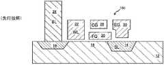
本発明は、不要な消去動作で同一セクタ内の他の物理ワードを過度に阻害することなく、フラッシュメモリデバイスが物理ワードをプログラムすることを可能にするメモリデバイス及び技術である。図1~図6は、本発明から利益を得ることができる、従来の不揮発性メモリセルのタイプの例を示す。例えば、図1に示すように、メモリセル10aは、半導体基板12に形成されたソース領域14(典型的には連続ソース線SLとして形成される)及びドレイン領域16を含み、それらの間にチャネル領域18を有する。浮遊ゲート20は、チャネル領域18の第1の部分の上方に絶縁されて形成され(並びに、チャネル領域18の第1の部分の導電性を制御して)、ソース領域14の一部分の上方にかけて形成される。ワード線ゲート22(典型的には、ワード線に結合される)は、チャネル領域18の第2の部分の上方に絶縁されて配設されている、(並びに、チャネル領域18の第2の部分の導電性を制御する)第1の部分と、上に向かって浮遊ゲート20の上方にかけて延在する第2の部分と、を有する。浮遊ゲート20及びワード線ゲート22は、ゲート酸化物によって基板12から絶縁される。ビット線コンタクト24は、(ビット線への電気的接続のために)ドレイン領域16に結合される。 The present invention is a memory device and technique that allows a flash memory device to program physical words without unduly disturbing other physical words in the same sector with unnecessary erase operations. 1-6 illustrate examples of conventional non-volatile memory cell types that can benefit from the present invention. For example, as shown in FIG. 1,
ワード線ゲート22に高正電圧をかけることによって、メモリセル10aは消去され(浮遊ゲートから電子が除去される)、これによって、ファウラーノルドハイム(Fowler-Nordheim)トンネリングを介して浮遊ゲート20からワード線ゲート22まで中間絶縁体を通って浮遊ゲート20の電子をトンネリングさせる。メモリセル10aは、ワード線ゲート22に正電圧をかけ、ソース領域14に正電圧をかけることによってプログラムされる(浮遊ゲート20に電子が印加される)。電子電流は、ソース領域14からドレイン領域16に向かって流れる。電子は加速し、ワード線ゲート22と浮遊ゲート20との間の間隙に達すると、発熱する。熱せられた電子の一部は、浮遊ゲート20からの静電引力に起因して、浮遊ゲート20にゲート酸化物を介して注入される(すなわち、ホットエレクトロン注入)。メモリセル10aは、ドレイン領域16及びワード線ゲート22に正の読み出し電圧をかける(これにより、ワード線ゲート22の下方のチャネル領域18の部分をオンにする)ことによって、読み出される。浮遊ゲート20が正に帯電する(すなわち、電子を消去する)と、浮遊ゲート20の下方のチャネル領域18の部分も同様にオンになり、電流はチャネル領域18を流れ、これは、消去された状態つまり「1」の状態として検知される。浮遊ゲート20が負に帯電する(すなわち、電子でプログラムされる)と、浮遊ゲート20の下方のチャネル領域の部分はほとんど又は完全にオフになり、電流はチャネル領域18を流れず(又はほとんど流れず)、これは、プログラムされた状態つまり「0」の状態として検出される。MLC動作で使用する場合、メモリセル10aを複数の中間状態にプログラムすることも可能である。
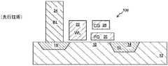
図2は、浮遊ゲート20の上方に絶縁されて配設されている制御ゲート(control gate、CG)28を追加した、図1のメモリセル10aと同様の別のメモリセル10bを示す。制御ゲート28は、プログラミング中に高電圧に、消去中に低電圧又は負電圧に、及び読み出し中に低電圧又は中範囲の電圧にバイアスされ得る。 FIG. 2 shows another
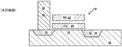
図3は、上に向かって浮遊ゲート20の上方にかけて延在する、ソース領域14の上方の消去ゲート30を追加した、図1のメモリセル10bと同様の4ゲートメモリセル10cを示す。消去は、消去ゲート30に高正電圧をかけるときに、浮遊ゲート20から消去ゲート30への電子トンネリングによって行われる。 FIG. 3 shows a four-gate
図4は、ワード線ゲート22が上に向かって浮遊ゲート20の上方にかけて延在しないことを除いて、図2のメモリセル10bと同様のメモリセル10dを示す。このメモリセルは、基板12を高電圧にバイアスさせ、制御ゲートCG28を低電圧又は負電圧にバイアスさせ、その結果、浮遊ゲート20から基板12へと電子をトンネリングさせることによって消去される。 FIG. 4 shows a
図5は、図3のメモリセル10cと同様であるが、浮遊ゲート20の上方に別個の制御ゲートが存在しないメモリセル10eを示す。 FIG. 5 shows a
図6は、スプリットゲートメモリセルではなく、積層ゲートメモリセルであるメモリセル10fを示す。この積層ゲート構成では、浮遊ゲート20は、チャネル領域18の全体の上方に延在する(また、導電性を制御する)。ワード線ゲート22は、浮遊ゲート20の上方に絶縁されて配設されている。このメモリセルは、上記と同様の方法でプログラムするために浮遊ゲートに結合された、ワード線ゲート22に正電圧をかけることによってプログラムされる。メモリセルは、ワード線ゲート22にゼロ電圧又は負電圧を、基板12に正電圧をかけて、浮遊ゲート20から基板12への電子のトンネリングを生じさせることによって消去される。メモリセルは、ワード線ゲート22にゼロ電圧又は正電圧をかけ、ドレイン領域16に正電圧をかけることによって読み出される。 FIG. 6 shows
図7は、不揮発性メモリセル10(図6の積層ゲートセル10fとして概略的に示すが、上記のメモリセル10a~10fのいずれかを含む任意の不揮発性メモリセルであり得る)の従来のアーキテクチャを示す。メモリセル10は、行及び列に配置される。各ワード線WLは、1行内に存在する全てのメモリセル10について、全てのワード線ゲート22を一緒に接続する。各ビット線BLは、1列内に存在する全てのメモリセル10について、ドレイン領域16の全てを一緒に接続する。各ソース線SLは、2つの隣接する行内に存在する全てのメモリセル10について、全てのソース領域14を一緒に接続する。各メモリセルに追加ゲートが存在する場合、追加の線が含まれ得る。メモリセル10はセクタSに分割され、各セクタは、セルのグループ(例えば、入出力グループ、すなわちIOグループ)を含む。各IOグループは、2つ以上の隣接する行の各々にn個のメモリセルを含む。各セクタの行の長さに沿って、p個のIOグループが存在する。メモリデバイスは、1回の消去動作でメモリセルのセクタ全体を一斉に消去するように構成されている。 FIG. 7 illustrates the conventional architecture of nonvolatile memory cell 10 (shown schematically as stacked
非限定的な例として、nは8に等しく、pは8に等しく、各IOグループの行数は、図7に示すように2(上行及び下行)であり得る。そのような場合、各IOグループに16個のメモリセル10(上行に8個のメモリセル10(1)~10(8)及び下行に8個のメモリセル10(9)~10(16))が存在する。また、2行のメモリセルには、8個のIOグループ(IO1、IO2...IO8)が存在する。そのようなアレイにおいて物理ワードを割り当てるための効率的な方法は、各IOグループから1つのメモリセル10を含むようにして、物理ワードを形成することである。例えば、各IOグループの上行の第1のメモリセル10(1)は、集合的に第1の物理ワードを形成することになる。各IOグループの上行の第2のメモリセル10(2)は、集合的に第2の物理ワードを形成するなどであり、各IOグループの下行の最終メモリセル10(2n)は、最終物理ワードを形成することになる。この例では、各物理ワードは、8個のメモリセル(各IOグループから1つ)を含み、図7に示すIOグループIO1~IO8には、16個の物理ワードが存在することになる。これは、物理ワードの各メモリセル10が異なるビット線に位置するために物理ワード全体をビット線BLで同時に読み出すことができるため、効率的である。しかしながら、従来の方法では、第1の物理ワードをデータでプログラムする場合、確実に全てのメモリセルを正確にプログラムできる(すなわち、以前のプログラミングがこれらのセルのプログラミングに影響を及ぼすことはない)ようにするために、最初に第1の物理ワードを消去する。しかしながら、第1の物理ワードを消去するためには、セクタ内の全ての物理ワードを必要に応じて消去し、再プログラムする。これには時間がかかり、メモリセルを過度に損耗させる。 As a non-limiting example, n equals 8, p equals 8, and the number of rows in each IO group can be 2 (upper row and lower row) as shown in FIG. In such a case, each IO group has 16 memory cells 10 (8 memory cells 10(1)-10(8) in the top row and 8 memory cells 10(9)-10(16) in the bottom row). exists. Also, there are eight IO groups (IO1, IO2, . . . IO8) in two rows of memory cells. An efficient way to allocate physical words in such an array is to include one
本発明は、IOグループ内の全物理ワードにインデックスビットメモリセルを提供することによって、従来のメモリセルアーキテクチャを改善する。図8に示すように、メモリアレイは、好ましくはIOグループIO1~IOpと同じメモリセルの行に、IOグループIO1~IOpのインデックスユニット40を含む。各インデックスユニット40は、物理ワードのうちの1つに関連付けられたインデックスメモリセル42を含む。具体的には、インデックスメモリセル42(1)を含むインデックスユニット40(1)は、IOグループIO1~IOp内のメモリセル10(1)の第1の物理ワードに対応し、インデックスメモリセル42(2)を含むインデックスユニット40(2)は、IOグループIO1~IOp内のメモリセル10(2)の第2の物理ワードに対応するなどであり、インデックスメモリセル42(2n)を含む最終インデックスユニット40(2n)は、IOグループIO1~IOp内のメモリセル10(2n)の最終物理ワードに対応する。各インデックスメモリセル42は、対応する物理ワードメモリセル10と同じ1行に位置することが好ましく、それにより、全てが同一動作でプログラム又は消去され得る。したがって、インデックスメモリセル42(1)~42(n)は上行に位置し、インデックスメモリセル42(n+1)~42(2n)は下行に位置する。しかしながら、同じ1列に2個のインデックスメモリセル42を位置付けないことが好ましいため、全てのインデックスメモリセル42は一斉に読み出され得る。したがって、各インデックスユニット40は、インデックスメモリセル42を含まないメモリセル行のためにダミーセル44を含む。したがって、図8の例では、インデックスユニット40(1)~40(n)は、上行にインデックスメモリセル42(1)~42(n)を含み、下行にダミーメモリセル44を含む。同様に、インデックスユニット40(n+1)~40(2n)は、下行にインデックスメモリセル42(n+1)~42(2n)を含み、上行にダミーメモリセル44を含む。ダミーメモリセル44は、データ記憶に使用されないメモリセルである。ダミーセル44が他のメモリセルの動作に干渉しないようにするために、各ダミーセル44は、好ましくは、各々のビット線BLへの電気的接続を有さない(例えば、当該ダミーメモリセルのビット線コンタクト24は、切断されている、又は形成すらされていない)。 The present invention improves upon conventional memory cell architectures by providing index bit memory cells for every physical word within an IO group. As shown in FIG. 8, the memory array includes
インデックスメモリセル42は、次に説明するメモリデバイスコントローラ66によって使用されるインデックスビット情報を記憶する。例示的なメモリデバイスのアーキテクチャを図10に示す。メモリデバイスは、前述の不揮発性メモリセル10、40、及び44のアレイ50を含み、アレイ50は、2つの分離したプレーン(プレーンA 52a及びプレーンB 52b)に隔離され得る。メモリセル10、40、44は、半導体基板12に複数の行及び列で配置され、単一のチップ上に形成される。不揮発性メモリセルのアレイに隣接して、アドレスをデコードし、選択されたメモリセルに対する読み出し動作、プログラム動作、及び消去動作中、様々なメモリセルゲート及び領域に様々な電圧を提供するために使用される、アドレスデコーダ及び電源回路(例えば、XDEC54(LV行デコーダ)、SLDRV56、YMUX58(列デコーダ)、HVDEC60(HV行デコーダ)、及びビット線コントローラ(BLINHCTL62)が存在する。列デコーダ58は、読み出し動作中にビット線47上の電流を測定するための、1つ以上のセンス増幅器を含む。コントローラ66(制御回路を含む)は、各種デバイス素子を制御して、本明細書に記載のメモリセル10及びインデックスメモリセル42の動作及び使用など各動作(プログラム、消去、読み出し)を対象メモリセルで実施する。電荷ポンプCHRGPMP64は、コントローラ66の制御下にて、メモリセルの読み出し、プログラム、及び消去に使用される様々な電圧を提供する。
コントローラ66は、本明細書に以下に記載するメモリセルのIOグループについてインデックスメモリセル42内のインデックスビット情報のプログラム、使用、及び消去を行うように構成されている。IOグループIO1~IOpを含むセクタが最初に構成されたとき、セクタ内の全てのメモリセル10及びインデックスメモリセル42は消去される(例えば、「1」状態へと消去される)。インデックスメモリセル42における「1」状態は、IOグループIO1~IOp内の全ての物理ワードが消去され、プログラム可能であることを示す(最初の予備消去も不要)。その後、1つ以上のデータの入力ワードがIOグループIO1~IOpにプログラムされ、記憶されるたびに、コントローラ66は、インデックスメモリセル42のステータスを最初に読み出す。そのステータスが、データの入力ワードを記憶するために十分な物理ワードが利用可能であることを示す場合、コントローラは、最初に消去動作を実行することなく、利用可能なメモリセルに当該データをプログラムする。しかしながら、そのステータスが、データの入力ワードを記憶するために利用可能な物理ワードが十分ではないことを示す場合、コントローラは、最初にセクタ消去を実行し、その結果、入力データは、IOグループIO1~IOpのメモリセル10にプログラムされ得る。
非限定的な例として、n=8、p=8、IOグループ行=2である図8を使用すると、セクタ消去後のIOグループIO1~IO8内の16個の全物理ワードについて、インデックスメモリセル42内のインデックスビット情報の初期値は全て1(1111111111111111)であり、全ての物理ワードが介在プログラミングなしで消去済みであり、したがって、更なる消去は不要でプログラミングに利用可能であることを示す。データの入力ワードがIOグループIO1~IO8にプログラムされる場合(図10のステップ1を参照)、コントローラ66はインデックスメモリセル42(1)~42(16)からインデックスビット情報を読み出す(図10のステップ2を参照)。これにより、16個の全物理ワードが消去され、プログラムに利用可能である(最初の予備消去は不要)と示されることになる。次いで、コントローラ66は、利用可能な物理ワードの1つ(例えば、第1の物理ワード)にデータのワードをプログラムし(図10のステップ3を参照)、その対応するインデックスメモリセル42を0状態にプログラムする(図10のステップ4を参照)。1及び/又は0の組み合わせからなるプログラミングデータ(例えば、セルの物理ワード)は、必ずしもメモリセルのグループ内の全メモリセルがそのプログラム状態にプログラムされることを意味するわけではないことに留意されたい。むしろ、本明細書で使用されるようにメモリセルのグループにデータをプログラムすることは、グループ内の一部のメモリセルがプログラム状態にプログラムされ得、その一方、グループ内の他のメモリセルは消去状態のままにされ得ることを意味し、その結果、メモリセルのグループのプログラム状態及び消去状態の組み合わせは、記憶されている入力データの0及び1を反映し、その逆も同様である。したがって、グループ内の全メモリセルをプログラム状態(「0」)にプログラムすることも含み得る(例えば、入力データが全て0である場合、又はコントローラが0のメモリセル状態と1のデータを相関させる場合は全て1)。同様に、グループ内の全メモリセルを消去状態(「1」)のままにすることも含み得る(例えば、入力データが全て1である場合、又はコントローラが1のメモリセル状態と0のデータを相関させる場合は全て0))。この時点で、IOグループIO1~IO8内の16個の全物理ワードについてのインデックスメモリセル42内のインデックスビット情報は(0111111111111111)であり、IOグループIO1~IO8内の全物理ワードが消去され、第1の物理ワードを除いてプログラミングに利用可能(予備消去の実行は不要)であることを示す。今後、コントローラが第1の物理ワードへのデータのプログラムを必要とすることがあれば、インデックスビット情報は、前回の消去動作のときからずっと物理ワードのプログラムされた状態にあり、当該物理ワードを再プログラムする前に別の消去動作を実行する必要があることをコントローラに示すことになる。 As a non-limiting example, using FIG. 8 where n=8, p=8, IO group row=2, for all 16 physical words in IO group IO1-IO8 after sector erase, the index memory cell The initial value of the index bit information in 42 is all ones (1111111111111111), indicating that all physical words have been erased without intervening programming and therefore are available for programming without further erasing. When an input word of data is programmed into IO groups IO1-IO8 (see
いずれの時点においても、コントローラ66は、インデックスビット情報を使用して、消去動作を実行する必要なく、依然としてプログラミングに利用可能である物理ワードを判定し、消去動作を実行することなくプログラミングを継続することができる。例えば、本実施例を継続すると、次のデータのワードがIOグループIO1~IO8にプログラムされる場合、インデックスビット情報は、第2の物理ワードが利用可能であることをコントローラに示し、第2の物理ワード及びそのインデックスメモリセル42がプログラムされる。その後、インデックスビット情報は(0011111111111111)となり、最初の2つの物理ワードは前回の消去動作以降にプログラムされており、他の物理ワードは、前回の消去動作以降にプログラムされておらず、最初に消去動作を実行することなくプログラミングに利用可能であることを示す。IOグループIO1~IO8内の物理ワードのプログラミングは、インデックスメモリセルがプログラミングを実行可能であること(すなわち、「1」)を示す、少なくとも1つの物理ワードが存在する限り、消去動作を全く行わずに継続することができる。インデックス情報が(0000000000000000)である場合、これは、前回の消去動作以降にIOグループIO1~IO8内の全物理ワードがプログラムされたことを示し、これらの物理ワードのいずれかがプログラムされるのであれば、最初に消去動作を実行する必要がある(図10のステップ5を参照)。IOグループIO1~IO8で消去動作が実行される場合、対応するインデックスメモリセル42も消去されて「1」状態にリセットされ(図10のステップ6を参照)、次いで、利用可能な物理ワードのうちの1つでプログラミングを開始することができる。 At any point in time, the
したがって、インデックスユニット40のインデックスメモリセル42に記憶されたインデックス情報は、前回の消去動作以降にプログラムされたIOグループIO1~IOp内の物理ワード(「0」状態で表される)及び前回の消去動作以降プログラムされていない物理ワード(「1」状態で表される)のリアルタイムステータスインジケータを(コントローラ66に、及び/又はオフチップのコントローラにも)提供する。これにより、コントローラ66は、最初に消去動作を行う必要なく、データをメモリセルに安全にプログラムすることができる。プログラム動作中に不要な消去動作を回避することは、より高速のプログラム動作をもたらし、メモリセルの不要な損耗を低減する。 Thus, the index information stored in the
インデックスメモリセル42内のインデックスビット情報はまた、読み出し動作中も使用することができる。具体的には、コントローラ66が読み出し動作を開始するときに、最新の更新された物理ワードのみにアクセスすることが望ましい場合がある。その場合、コントローラ66は、最初に関連するインデックスメモリセル42を読み出して、各々の前回の消去動作以降で直近にプログラムされた複数の物理ワードを判定することができる。次いで、コントローラは、旧版の(最新のプログラムが行われていない)又は各々の前回の消去動作以降にプログラムされていないかのいずれかである他の物理ワードの読み出しを回避することによって、読み出し動作を円滑にすることができる。例えば、インデックス情報が(0001111111111111)であり、物理ワード3が直近にプログラムされたワードであることを表すとき(物理ワードがインデックス情報によって順番にプログラムされると仮定した場合)、物理ワード1及び2は旧版であり、物理ワード4~16は未使用である。したがって、読み出し動作では、物理ワード3のみが読み出される。 The index bit information in
図8は、まとめてグループ化されたインデックスユニットを示すが、必ずしもそうである必要はない。例えば、図11は、列ごとに1つのインデックスユニット40がIOグループのうちの1つに直接隣接して位置する代替実施形態を示す。この構成は、インデックスユニットとIOグループとの間でソース線のピックアップを共有することによってアレイ効率を向上することができる。対照的に、図7の構成では、各インデックスビットは専用ソース線のピックアップを必要とし、そうでなければ、全てのインデックスメモリセル42が同時に読み出されるときに、IRが大幅に低下し得る。対応するIOグループのメモリセル10と同一の行にインデックスユニット40を配置することが好ましく、その結果、対応するメモリセル10のプログラム及び消去と同じ動作を使用してプログラム及び消去を行うことができる。しかしながら、IOグループIO1~IOpのインデックスユニット40は、メモリアレイ内の任意の位置に、又は更には同一チップ上の別個の位置に配置され得る。 Although FIG. 8 shows index units grouped together, this need not be the case. For example, FIG. 11 shows an alternative embodiment in which one
本発明は、本明細書に図示された上記実施形態に限定されるものではなく、任意の特許請求の範囲の範疇に収まるあらゆる変形例を包含することが理解されよう。例えば、本明細書における本発明への言及は、特許請求の範囲又は特許請求項の用語の限定を意図するものではなく、代わりに特許請求の範囲の1つ以上によって網羅され得る1つ以上の特徴に言及するにすぎない。更に、図は、2行及び1セットのIOグループIO1~IOpのみを含むセクタを示すが、メモリセルのセクタは、3行以上を含み得、複数セットのIOグループIO1~IOpを含み得る。同様に、1セットのIOグループIO1~IOpが2メモリセル行を含むように示されているが、1メモリセル行のみ又は3行以上のメモリセルを含み得る。また、インデックスユニット40は、対応するIOグループIO1~IOpと同数のメモリセル行を含むように示されているが、インデックスユニット40内のメモリセル行の数は、対応するIOグループのメモリセル行の数とは異なり得る。インデックスセルは、初期消去状態を有し、その後、関連付けられた物理ワードがプログラムされると、プログラム状態にプログラムされるものとして上述されているが、その反対に、インデックスセルは最初にプログラム状態に設定されてプログラム可能であることを示し、その関連付けられた物理ワードがプログラムされると、消去状態に設定される(しかしながら、これには、インデックスメモリセルを個別に消去する能力を必要とすることになる)場合もあり得る。上記で説明した材料、プロセス、及び数値の実施例は、単に例示的なものであり、特許請求の範囲を限定するものとみなされるべきではない。更に、特許請求の範囲及び本明細書から明らかであるように、全ての方法ステップが例示された、又は特許請求された正確な順序で実行される必要はなく、むしろ、本発明のメモリデバイスの適切な形成又は動作が可能になる任意の順序で実行される。単一の材料層は、かかる又は類似の材料から構成される多数の層として形成することができ、そして、逆もまた同様である。最後に、本明細書で使用される、「形成」及び「形成される」という用語は、材料堆積、材料化成、又は開示又は特許請求される材料を提供する際の任意の他の技法を含むものとする。 It will be appreciated that the present invention is not limited to the above-described embodiments illustrated herein, but encompasses all modifications that fall within the scope of any claims. For example, references to the present invention herein are not intended to limit the scope of the claims or the claim terms, but instead one or more of the claims that may be covered by one or more of the claims. Just mention the features. Further, although the figure shows a sector containing only two rows and one set of IO groups IO1-IOp, a sector of memory cells may contain more than two rows and may contain multiple sets of IO groups IO1-IOp. Similarly, although a set of IO groups IO1-IOp are shown as containing two rows of memory cells, they may contain only one row of memory cells or more than two rows of memory cells. Also, although
インデックスメモリセル42は、次に説明するメモリデバイスコントローラ66によって使用されるインデックスビット情報を記憶する。例示的なメモリデバイスのアーキテクチャを図9に示す。メモリデバイスは、前述の不揮発性メモリセル10、40、及び44のアレイ50を含み、アレイ50は、2つの分離したプレーン(プレーンA 52a及びプレーンB 52b)に隔離され得る。メモリセル10、40、44は、半導体基板12に複数の行及び列で配置され、単一のチップ上に形成される。不揮発性メモリセルのアレイに隣接して、アドレスをデコードし、選択されたメモリセルに対する読み出し動作、プログラム動作、及び消去動作中、様々なメモリセルゲート及び領域に様々な電圧を提供するために使用される、アドレスデコーダ及び電源回路(例えば、XDEC54(LV行デコーダ)、SLDRV56、YMUX58(列デコーダ)、HVDEC60(HV行デコーダ)、及びビット線コントローラ(BLINHCTL62))が存在する。列デコーダ58は、読み出し動作中にビット線47上の電流を測定するための、1つ以上のセンス増幅器を含む。コントローラ66(制御回路を含む)は、各種デバイス素子を制御して、本明細書に記載のメモリセル10及びインデックスメモリセル42の動作及び使用など各動作(プログラム、消去、読み出し)を対象メモリセルで実施する。電荷ポンプCHRGPMP64は、コントローラ66の制御下にて、メモリセルの読み出し、プログラム、及び消去に使用される様々な電圧を提供する。
Claims (21)
Translated fromJapanese複数の不揮発性メモリセルを含むメモリアレイと、
前記複数の不揮発性メモリセルのうちの異なる1つと各々関連付けられた複数のインデックスメモリセルと、
コントローラであって、
前記複数の不揮発性メモリセルを消去すること、
前記インデックスメモリセルの各々を第1の状態に設定すること、
前記メモリアレイに第1のデータを、
前記複数のインデックスメモリセルを読み出し、前記インデックスメモリセルの第1のインデックスメモリセルが前記第1の状態にあると判定すること、
前記インデックスメモリセルの前記第1のインデックスメモリセルと関連付けられた前記複数の不揮発性メモリセルに前記第1のデータをプログラムすること、及び
前記インデックスメモリセルの前記第1のインデックスメモリセルを、前記第1の状態とは異なる第2の状態に設定すること、によってプログラムすること、を行うように構成されている、コントローラと、を備える、メモリデバイス。a memory device,
a memory array including a plurality of nonvolatile memory cells;
a plurality of index memory cells each associated with a different one of the plurality of nonvolatile memory cells;
is a controller,
erasing the plurality of non-volatile memory cells;
setting each of the index memory cells to a first state;
first data in the memory array;
reading the plurality of index memory cells and determining that a first index memory cell of the index memory cells is in the first state;
programming the first data into the plurality of nonvolatile memory cells associated with the first index memory cell of the index memory cells; and programming the first index memory cell of the index memory cells to the a controller configured to program by setting to a second state different from the first state.
前記インデックスメモリセルの前記第1のインデックスメモリセルを前記第2の状態に設定することは、前記インデックスメモリセルの前記第1のインデックスメモリセルを前記プログラム状態にプログラムすることを含む、請求項2に記載のデバイス。setting each of the index memory cells to a first state includes erasing each of the index memory cells to the erased state;
3. The step of setting said first index memory cell of said index memory cells to said second state comprises programming said first index memory cell of said index memory cells to said programmed state. devices described in .
前記メモリアレイに第2のデータを、
前記複数のインデックスメモリセルを読み出し、前記インデックスメモリセルの第2のインデックスメモリセルが前記第1の状態にあると判定すること、
前記インデックスメモリセルの前記第2のインデックスメモリセルと関連付けられた前記複数の不揮発性メモリセルに前記第2のデータをプログラムすること、及び
前記インデックスメモリセルの前記第2のインデックスメモリセルを前記第2の状態に設定すること、によってプログラムするように更に構成されている、請求項1に記載のデバイス。The controller is
second data in the memory array;
reading the plurality of index memory cells and determining that a second of the index memory cells is in the first state;
programming the second data into the plurality of non-volatile memory cells associated with the second index memory cell of the index memory cells; 2. The device of claim 1, further configured to program by setting a state of 2.
前記複数のインデックスメモリセルを読み出し、前記インデックスメモリセルの全てが前記第2の状態にあると判定すること、並びにそれに応じて、
前記複数の不揮発性メモリセルを消去すること、及び
前記インデックスメモリセルの各々を前記第1の状態に設定すること、を行うように更に構成されている、請求項1に記載のデバイス。The controller is
reading the plurality of index memory cells and determining that all of the index memory cells are in the second state;
2. The device of claim 1, further configured to: erase the plurality of non-volatile memory cells; and set each of the index memory cells to the first state.
前記メモリアレイに第2のデータを、
前記複数のインデックスメモリセルを読み出し、前記インデックスメモリセルの全てが前記第2の状態にあると判定すること、
前記複数の不揮発性メモリセルを消去すること、
前記インデックスメモリセルの各々を前記第1の状態に設定すること、
前記インデックスメモリセルのうちの1つと関連付けられた前記複数の不揮発性メモリセルに前記第2のデータをプログラムすること、及び
前記インデックスメモリセルのうちの前記関連付けられたインデックスメモリセルを前記第2の状態に設定すること、によってプログラムするように更に構成されている、請求項1に記載のデバイス。The controller is
second data in the memory array;
reading the plurality of index memory cells and determining that all of the index memory cells are in the second state;
erasing the plurality of non-volatile memory cells;
setting each of the index memory cells to the first state;
programming the second data into the plurality of non-volatile memory cells associated with one of the index memory cells; and programming the associated one of the index memory cells to the second 2. The device of claim 1, further configured to program by setting a state.
前記インデックスメモリセルの前記第1のインデックスメモリセルと関連付けられた前記複数の不揮発性メモリセル内の前記不揮発性メモリセルの全て、及び前記インデックスメモリセルの前記第1のインデックスメモリセルは、前記行のうちの1行に位置する、請求項1に記載のデバイス。the plurality of memory cells arranged in rows and columns that also include the plurality of index memory cells;
all of the non-volatile memory cells in the plurality of non-volatile memory cells associated with the first index memory cell of the index memory cells and the first index memory cell of the index memory cells in the row 2. The device of claim 1, located in a row of .
前記IOグループごとに、前記IOグループ内の前記不揮発性メモリセルの一部は前記行の第1の行に位置し、前記IOグループ内の他の前記不揮発性メモリセルは前記行の第2の行に位置し、
前記インデックスメモリセルの一部は前記第1の行に位置し、他の前記インデックスメモリセルは前記第2の行に位置する、請求項8に記載のデバイス。the plurality of memory cells arranged in IO groups, each of the IO groups including only one nonvolatile memory cell from each of the plurality of nonvolatile memory cells;
For each IO group, some of the non-volatile memory cells within the IO group are located in the first row of the rows and other of the non-volatile memory cells within the IO group are located in the second row of the rows. located on the line
9. The device of claim 8, wherein some of said index memory cells are located in said first row and other said index memory cells are located in said second row.
前記第2の行に位置する前記インデックスメモリセルごとに、前記メモリデバイスは、前記第1の行かつ前記インデックスメモリセルを含む同一列に位置するダミーメモリセルを更に含む、請求項9に記載のデバイス。for each index memory cell located in the first row, the memory device further includes a dummy memory cell located in the second row and the same column containing the index memory cell;
10. The claim 9, wherein for each said index memory cell located in said second row, said memory device further comprises a dummy memory cell located in said first row and in the same column containing said index memory cell. device.
任意の2つのIOグループごとに、前記インデックスメモリセルのうちの少なくとも1つは、前記2つのIOグループの前記2つの複数の列の間である前記列のうちの1つに位置する、請求項9に記載のデバイス。each of the IO groups is located in a plurality of the columns that do not contain any of the other IO groups;
4. The claim wherein for any two IO groups, at least one of said index memory cells is located in one of said columns that is between said two plurality of columns of said two IO groups. 9. The device according to 9.
前記複数の不揮発性メモリセルを消去するステップと、
前記インデックスメモリセルの各々を第1の状態に設定するステップと、
前記メモリアレイに第1のデータを、
前記複数のインデックスメモリセルを読み出し、前記インデックスメモリセルの第1のインデックスメモリセルが前記第1の状態にあると判定すること、
前記インデックスメモリセルの前記第1のインデックスメモリセルと関連付けられた前記複数の不揮発性メモリセルに前記第1のデータをプログラムすること、及び
前記インデックスメモリセルの前記第1のインデックスメモリセルを、前記第1の状態とは異なる第2の状態に設定すること、によってプログラムするステップと、を含む、方法。1. A method of operating a memory device comprising a memory array comprising a plurality of non-volatile memory cells and a plurality of index memory cells each associated with a different one of said plurality of non-volatile memory cells, comprising:
erasing the plurality of non-volatile memory cells;
setting each of the index memory cells to a first state;
first data in the memory array;
reading the plurality of index memory cells and determining that a first index memory cell of the index memory cells is in the first state;
programming the first data into the plurality of nonvolatile memory cells associated with the first index memory cell of the index memory cells; and programming the first index memory cell of the index memory cells to the setting to a second state different from the first state.
前記インデックスメモリセルの前記第1のインデックスメモリセルを前記第2の状態に設定することは、前記インデックスメモリセルの前記第1のインデックスメモリセルを前記プログラム状態にプログラムすることを含む、請求項13に記載の方法。setting each of the index memory cells to a first state includes erasing each of the index memory cells to the erased state;
14. The setting of the first index memory cell of the index memory cells to the second state comprises programming the first index memory cell of the index memory cells to the programmed state. The method described in .
前記複数のインデックスメモリセルを読み出し、前記インデックスメモリセルの第2のインデックスメモリセルが前記第1の状態にあると判定すること、
前記インデックスメモリセルの前記第2のインデックスメモリセルと関連付けられた前記複数の不揮発性メモリセルに前記第2のデータをプログラムすること、及び
前記インデックスメモリセルの前記第2のインデックスメモリセルを前記第2の状態に設定すること、によってプログラムするステップを更に含む、請求項12に記載の方法。second data in the memory array;
reading the plurality of index memory cells and determining that a second of the index memory cells is in the first state;
programming the second data into the plurality of non-volatile memory cells associated with the second index memory cell of the index memory cells; 13. The method of claim 12, further comprising programming by setting a state of 2.
前記複数の不揮発性メモリセルを消去するステップ、及び
前記インデックスメモリセルの各々を前記第1の状態に設定するステップを更に含む、請求項12に記載の方法。reading the plurality of index memory cells and determining that all of the index memory cells are in the second state; and, accordingly,
13. The method of claim 12, further comprising: erasing said plurality of non-volatile memory cells; and setting each of said index memory cells to said first state.
前記複数のインデックスメモリセルを読み出し、前記インデックスメモリセルの全てが前記第2の状態にあると判定すること、
前記複数の不揮発性メモリセルを消去すること、
前記インデックスメモリセルの各々を前記第1の状態に設定すること、
前記インデックスメモリセルのうちの1つと関連付けられた前記複数の不揮発性メモリセルに前記第2のデータをプログラムすること、及び
前記インデックスメモリセルのうちの前記関連付けられたインデックスメモリセルを前記第2の状態に設定すること、によってプログラムするステップを更に含む、請求項12に記載の方法。second data in the memory array;
reading the plurality of index memory cells and determining that all of the index memory cells are in the second state;
erasing the plurality of non-volatile memory cells;
setting each of the index memory cells to the first state;
programming the second data into the plurality of non-volatile memory cells associated with one of the index memory cells; and programming the associated one of the index memory cells to the second 13. The method of claim 12, further comprising programming by setting a state.
前記インデックスメモリセルの前記第1のインデックスメモリセルと関連付けられた前記複数の不揮発性メモリセル内の前記不揮発性メモリセルの全て、及び前記インデックスメモリセルの前記第1のインデックスメモリセルは、前記行のうちの1行に位置する、請求項12に記載の方法。the plurality of memory cells arranged in rows and columns that also include the plurality of index memory cells;
all of the non-volatile memory cells in the plurality of non-volatile memory cells associated with the first index memory cell of the index memory cells and the first index memory cell of the index memory cells in the row 13. The method of claim 12, located in a row of .
前記IOグループごとに、前記IOグループ内の前記不揮発性メモリセルの一部は前記行の第1の行に位置し、前記IOグループ内の他の前記不揮発性メモリセルは前記行の第2の行に位置し、
前記インデックスメモリセルの一部は前記第1の行に位置し、他の前記インデックスメモリセルは前記第2の行に位置する、請求項18に記載の方法。the plurality of memory cells arranged in IO groups, each of the IO groups including only one nonvolatile memory cell from each of the plurality of nonvolatile memory cells;
For each IO group, some of the non-volatile memory cells within the IO group are located in the first row of the rows and other of the non-volatile memory cells within the IO group are located in the second row of the rows. located on the line
19. The method of claim 18, wherein some of said index memory cells are located in said first row and other said index memory cells are located in said second row.
前記第2の行に位置する前記インデックスメモリセルごとに、前記メモリデバイスは、前記第1の行かつ前記インデックスメモリセルを含む同一列に位置するダミーメモリセルを更に含む、請求項19に記載の方法。for each index memory cell located in the first row, the memory device further includes a dummy memory cell located in the second row and the same column containing the index memory cell;
20. The claim 19, wherein for each said index memory cell located in said second row, said memory device further comprises a dummy memory cell located in said first row and in the same column containing said index memory cell. Method.
任意の2つのIOグループごとに、前記インデックスメモリセルのうちの少なくとも1つは、前記2つのIOグループの前記2つの複数の列の間である前記列のうちの1つに位置する、請求項19に記載の方法。each of the IO groups is located in a plurality of the columns that do not contain any of the other IO groups;
4. The claim wherein for any two IO groups, at least one of said index memory cells is located in one of said columns that is between said two plurality of columns of said two IO groups. 19. The method according to 19.
Applications Claiming Priority (5)
| Application Number | Priority Date | Filing Date | Title |
|---|---|---|---|
| CN201910875107.3 | 2019-09-17 | ||
| CN201910875107.3ACN112530494B (en) | 2019-09-17 | 2019-09-17 | Nonvolatile memory device with stored index information |
| US16/813,317 | 2020-03-09 | ||
| US16/813,317US11074980B2 (en) | 2019-09-17 | 2020-03-09 | Non-volatile memory device with stored index information |
| PCT/US2020/022192WO2021055006A1 (en) | 2019-09-17 | 2020-03-11 | Non-volatile memory device with stored index information |
Publications (2)
| Publication Number | Publication Date |
|---|---|
| JP2022548154Atrue JP2022548154A (en) | 2022-11-16 |
| JP7349564B2 JP7349564B2 (en) | 2023-09-22 |
Family
ID=74869695
Family Applications (1)
| Application Number | Title | Priority Date | Filing Date |
|---|---|---|---|
| JP2022517161AActiveJP7349564B2 (en) | 2019-09-17 | 2020-03-11 | non-volatile memory device with stored index information |
Country Status (7)
| Country | Link |
|---|---|
| US (1) | US11074980B2 (en) |
| EP (1) | EP4032089B1 (en) |
| JP (1) | JP7349564B2 (en) |
| KR (1) | KR102687843B1 (en) |
| CN (1) | CN112530494B (en) |
| TW (1) | TWI744875B (en) |
| WO (1) | WO2021055006A1 (en) |
Citations (6)
| Publication number | Priority date | Publication date | Assignee | Title |
|---|---|---|---|---|
| US5517453A (en)* | 1994-09-15 | 1996-05-14 | National Semiconductor Corporation | Memory with multiple erase modes |
| JPH10302490A (en)* | 1997-04-25 | 1998-11-13 | Mitsubishi Electric Corp | Read-only semiconductor memory device |
| JP2002508862A (en)* | 1997-03-31 | 2002-03-19 | レクサー メディア,インコーポレイテッド | Moving sectors in blocks in flash memory |
| US20130279250A1 (en)* | 2012-04-19 | 2013-10-24 | Samsung Electronics Co., Ltd. | Nonvolatile memory device with flag cells and user device including the same |
| US20170062057A1 (en)* | 2015-08-28 | 2017-03-02 | SK Hynix Inc. | Nonvolatile memory device, data storage device including the same, and operating method thereof |
| US20190103165A1 (en)* | 2017-09-29 | 2019-04-04 | SK Hynix Inc. | Non-volatile memory device, method for operating the same and data storage device including the same |
Family Cites Families (14)
| Publication number | Priority date | Publication date | Assignee | Title |
|---|---|---|---|---|
| US5029130A (en) | 1990-01-22 | 1991-07-02 | Silicon Storage Technology, Inc. | Single transistor non-valatile electrically alterable semiconductor memory device |
| US20050144516A1 (en)* | 2003-12-30 | 2005-06-30 | Gonzalez Carlos J. | Adaptive deterministic grouping of blocks into multi-block units |
| EP2289069B1 (en)* | 2008-06-12 | 2016-12-28 | SanDisk Technologies LLC | Nonvolatile memory and method with index programming and reduced verify |
| US7800945B2 (en)* | 2008-06-12 | 2010-09-21 | Sandisk Corporation | Method for index programming and reduced verify in nonvolatile memory |
| US7826271B2 (en)* | 2008-06-12 | 2010-11-02 | Sandisk Corporation | Nonvolatile memory with index programming and reduced verify |
| US8004888B2 (en) | 2008-09-22 | 2011-08-23 | Spansion Llc | Flash mirror bit architecture using single program and erase entity as logical cell |
| KR101504338B1 (en)* | 2009-03-04 | 2015-03-23 | 삼성전자주식회사 | Operating method of nonvolatile memory device |
| US8804429B2 (en) | 2011-12-08 | 2014-08-12 | Silicon Storage Technology, Inc. | Non-volatile memory device and a method of programming such device |
| US9286160B2 (en)* | 2014-02-07 | 2016-03-15 | Stmicroelectronics S.R.L. | System and method for phase change memory with erase flag cells |
| JP2018005959A (en) | 2016-06-30 | 2018-01-11 | 東芝メモリ株式会社 | Memory system and writing method |
| KR102578153B1 (en) | 2016-08-25 | 2023-09-14 | 에스케이하이닉스 주식회사 | Memory system and operating method of the memory system |
| KR102707003B1 (en)* | 2016-08-25 | 2024-09-19 | 에스케이하이닉스 주식회사 | Memory system and operating method of the memory system |
| FR3055992A1 (en)* | 2016-09-09 | 2018-03-16 | Proton World International N.V. | INDEX MANAGEMENT IN A FLASH MEMORY |
| JP6387134B1 (en) | 2017-03-09 | 2018-09-05 | ウィンボンド エレクトロニクス コーポレーション | Semiconductor memory device |
- 2019
- 2019-09-17CNCN201910875107.3Apatent/CN112530494B/enactiveActive
- 2020
- 2020-03-09USUS16/813,317patent/US11074980B2/enactiveActive
- 2020-03-11WOPCT/US2020/022192patent/WO2021055006A1/ennot_activeCeased
- 2020-03-11KRKR1020227002500Apatent/KR102687843B1/enactiveActive
- 2020-03-11EPEP20717431.9Apatent/EP4032089B1/enactiveActive
- 2020-03-11JPJP2022517161Apatent/JP7349564B2/enactiveActive
- 2020-04-27TWTW109113983Apatent/TWI744875B/enactive
Patent Citations (6)
| Publication number | Priority date | Publication date | Assignee | Title |
|---|---|---|---|---|
| US5517453A (en)* | 1994-09-15 | 1996-05-14 | National Semiconductor Corporation | Memory with multiple erase modes |
| JP2002508862A (en)* | 1997-03-31 | 2002-03-19 | レクサー メディア,インコーポレイテッド | Moving sectors in blocks in flash memory |
| JPH10302490A (en)* | 1997-04-25 | 1998-11-13 | Mitsubishi Electric Corp | Read-only semiconductor memory device |
| US20130279250A1 (en)* | 2012-04-19 | 2013-10-24 | Samsung Electronics Co., Ltd. | Nonvolatile memory device with flag cells and user device including the same |
| US20170062057A1 (en)* | 2015-08-28 | 2017-03-02 | SK Hynix Inc. | Nonvolatile memory device, data storage device including the same, and operating method thereof |
| US20190103165A1 (en)* | 2017-09-29 | 2019-04-04 | SK Hynix Inc. | Non-volatile memory device, method for operating the same and data storage device including the same |
Also Published As
| Publication number | Publication date |
|---|---|
| CN112530494B (en) | 2024-06-25 |
| CN112530494A (en) | 2021-03-19 |
| KR102687843B1 (en) | 2024-07-23 |
| WO2021055006A1 (en) | 2021-03-25 |
| TWI744875B (en) | 2021-11-01 |
| US20210082517A1 (en) | 2021-03-18 |
| EP4032089A1 (en) | 2022-07-27 |
| US11074980B2 (en) | 2021-07-27 |
| EP4032089B1 (en) | 2023-07-26 |
| TW202113848A (en) | 2021-04-01 |
| KR20220024935A (en) | 2022-03-03 |
| JP7349564B2 (en) | 2023-09-22 |
Similar Documents
| Publication | Publication Date | Title |
|---|---|---|
| KR100960352B1 (en) | How to Erase Flash Memory Using Line Erase | |
| CN100433193C (en) | Charge injection | |
| US20060221682A1 (en) | Floating gate memory with split-gate read transistor and split gate program transistor memory cells and method for making the same | |
| US9218886B2 (en) | String dependent parameter setup | |
| US7382651B2 (en) | Nonvolatile semiconductor memory device | |
| CN100444284C (en) | Nonvolatile semiconductor memory device with shortened erasing time | |
| JP7105989B2 (en) | Programming memory cells with gates capacitively coupled to floating gates | |
| TW200304147A (en) | Overerase correction method | |
| KR100746292B1 (en) | Nonvolatile memory device | |
| TWI567741B (en) | System and method to reduce disturbances during programming of flash memory cells | |
| KR102431098B1 (en) | Removable Gate Flash Memory Array with Byte Erase Operation | |
| JP2011198437A (en) | Nonvolatile semiconductor memory device | |
| JP2005011490A (en) | Semiconductor device | |
| CN106251899B (en) | Non-volatile memory device | |
| JP2001307492A (en) | Erase method for nonvolatile semiconductor memory device | |
| TWI687928B (en) | System and method for minimizing floating gate to floating gate coupling effects during programming in flash memory | |
| US7433244B2 (en) | Flash memory device and related erase operation | |
| CN111916129A (en) | Nonvolatile memory device, operating method thereof, and memory system | |
| US8767474B2 (en) | Nonvolatile memory device and method for controlling the same | |
| JP7349564B2 (en) | non-volatile memory device with stored index information | |
| JP2011216169A (en) | Semiconductor memory | |
| JP5792878B2 (en) | Semiconductor memory device | |
| JP2006331476A (en) | Nonvolatile semiconductor memory device |
Legal Events
| Date | Code | Title | Description |
|---|---|---|---|
| A521 | Request for written amendment filed | Free format text:JAPANESE INTERMEDIATE CODE: A523 Effective date:20220616 | |
| A621 | Written request for application examination | Free format text:JAPANESE INTERMEDIATE CODE: A621 Effective date:20220616 | |
| A131 | Notification of reasons for refusal | Free format text:JAPANESE INTERMEDIATE CODE: A131 Effective date:20230516 | |
| A977 | Report on retrieval | Free format text:JAPANESE INTERMEDIATE CODE: A971007 Effective date:20230517 | |
| A521 | Request for written amendment filed | Free format text:JAPANESE INTERMEDIATE CODE: A523 Effective date:20230816 | |
| TRDD | Decision of grant or rejection written | ||
| A01 | Written decision to grant a patent or to grant a registration (utility model) | Free format text:JAPANESE INTERMEDIATE CODE: A01 Effective date:20230905 | |
| A61 | First payment of annual fees (during grant procedure) | Free format text:JAPANESE INTERMEDIATE CODE: A61 Effective date:20230911 | |
| R150 | Certificate of patent or registration of utility model | Ref document number:7349564 Country of ref document:JP Free format text:JAPANESE INTERMEDIATE CODE: R150 |