JP2022548081A - Trapezoidal interconnect with tight BEOL pitch - Google Patents
Trapezoidal interconnect with tight BEOL pitchDownload PDFInfo
- Publication number
- JP2022548081A JP2022548081AJP2022516311AJP2022516311AJP2022548081AJP 2022548081 AJP2022548081 AJP 2022548081AJP 2022516311 AJP2022516311 AJP 2022516311AJP 2022516311 AJP2022516311 AJP 2022516311AJP 2022548081 AJP2022548081 AJP 2022548081A
- Authority
- JP
- Japan
- Prior art keywords
- trench
- conformal
- barrier layer
- dielectric
- conductor
- Prior art date
- Legal status (The legal status is an assumption and is not a legal conclusion. Google has not performed a legal analysis and makes no representation as to the accuracy of the status listed.)
- Granted
Links
Images


Classifications
- H—ELECTRICITY
- H01—ELECTRIC ELEMENTS
- H01L—SEMICONDUCTOR DEVICES NOT COVERED BY CLASS H10
- H01L23/00—Details of semiconductor or other solid state devices
- H01L23/52—Arrangements for conducting electric current within the device in operation from one component to another, i.e. interconnections, e.g. wires, lead frames
- H01L23/522—Arrangements for conducting electric current within the device in operation from one component to another, i.e. interconnections, e.g. wires, lead frames including external interconnections consisting of a multilayer structure of conductive and insulating layers inseparably formed on the semiconductor body
- H01L23/532—Arrangements for conducting electric current within the device in operation from one component to another, i.e. interconnections, e.g. wires, lead frames including external interconnections consisting of a multilayer structure of conductive and insulating layers inseparably formed on the semiconductor body characterised by the materials
- H01L23/53204—Conductive materials
- H01L23/53209—Conductive materials based on metals, e.g. alloys, metal silicides
- H—ELECTRICITY
- H01—ELECTRIC ELEMENTS
- H01L—SEMICONDUCTOR DEVICES NOT COVERED BY CLASS H10
- H01L21/00—Processes or apparatus adapted for the manufacture or treatment of semiconductor or solid state devices or of parts thereof
- H01L21/70—Manufacture or treatment of devices consisting of a plurality of solid state components formed in or on a common substrate or of parts thereof; Manufacture of integrated circuit devices or of parts thereof
- H01L21/71—Manufacture of specific parts of devices defined in group H01L21/70
- H01L21/768—Applying interconnections to be used for carrying current between separate components within a device comprising conductors and dielectrics
- H01L21/76801—Applying interconnections to be used for carrying current between separate components within a device comprising conductors and dielectrics characterised by the formation and the after-treatment of the dielectrics, e.g. smoothing
- H01L21/76802—Applying interconnections to be used for carrying current between separate components within a device comprising conductors and dielectrics characterised by the formation and the after-treatment of the dielectrics, e.g. smoothing by forming openings in dielectrics
- H01L21/76804—Applying interconnections to be used for carrying current between separate components within a device comprising conductors and dielectrics characterised by the formation and the after-treatment of the dielectrics, e.g. smoothing by forming openings in dielectrics by forming tapered via holes
- H—ELECTRICITY
- H01—ELECTRIC ELEMENTS
- H01L—SEMICONDUCTOR DEVICES NOT COVERED BY CLASS H10
- H01L21/00—Processes or apparatus adapted for the manufacture or treatment of semiconductor or solid state devices or of parts thereof
- H01L21/70—Manufacture or treatment of devices consisting of a plurality of solid state components formed in or on a common substrate or of parts thereof; Manufacture of integrated circuit devices or of parts thereof
- H01L21/71—Manufacture of specific parts of devices defined in group H01L21/70
- H01L21/768—Applying interconnections to be used for carrying current between separate components within a device comprising conductors and dielectrics
- H01L21/76801—Applying interconnections to be used for carrying current between separate components within a device comprising conductors and dielectrics characterised by the formation and the after-treatment of the dielectrics, e.g. smoothing
- H01L21/76802—Applying interconnections to be used for carrying current between separate components within a device comprising conductors and dielectrics characterised by the formation and the after-treatment of the dielectrics, e.g. smoothing by forming openings in dielectrics
- H01L21/76816—Aspects relating to the layout of the pattern or to the size of vias or trenches
- H—ELECTRICITY
- H01—ELECTRIC ELEMENTS
- H01L—SEMICONDUCTOR DEVICES NOT COVERED BY CLASS H10
- H01L21/00—Processes or apparatus adapted for the manufacture or treatment of semiconductor or solid state devices or of parts thereof
- H01L21/70—Manufacture or treatment of devices consisting of a plurality of solid state components formed in or on a common substrate or of parts thereof; Manufacture of integrated circuit devices or of parts thereof
- H01L21/71—Manufacture of specific parts of devices defined in group H01L21/70
- H01L21/768—Applying interconnections to be used for carrying current between separate components within a device comprising conductors and dielectrics
- H01L21/76838—Applying interconnections to be used for carrying current between separate components within a device comprising conductors and dielectrics characterised by the formation and the after-treatment of the conductors
- H01L21/76841—Barrier, adhesion or liner layers
- H01L21/76843—Barrier, adhesion or liner layers formed in openings in a dielectric
- H—ELECTRICITY
- H01—ELECTRIC ELEMENTS
- H01L—SEMICONDUCTOR DEVICES NOT COVERED BY CLASS H10
- H01L23/00—Details of semiconductor or other solid state devices
- H01L23/52—Arrangements for conducting electric current within the device in operation from one component to another, i.e. interconnections, e.g. wires, lead frames
- H01L23/522—Arrangements for conducting electric current within the device in operation from one component to another, i.e. interconnections, e.g. wires, lead frames including external interconnections consisting of a multilayer structure of conductive and insulating layers inseparably formed on the semiconductor body
- H01L23/528—Layout of the interconnection structure
- H01L23/5283—Cross-sectional geometry
- H—ELECTRICITY
- H01—ELECTRIC ELEMENTS
- H01L—SEMICONDUCTOR DEVICES NOT COVERED BY CLASS H10
- H01L23/00—Details of semiconductor or other solid state devices
- H01L23/52—Arrangements for conducting electric current within the device in operation from one component to another, i.e. interconnections, e.g. wires, lead frames
- H01L23/522—Arrangements for conducting electric current within the device in operation from one component to another, i.e. interconnections, e.g. wires, lead frames including external interconnections consisting of a multilayer structure of conductive and insulating layers inseparably formed on the semiconductor body
- H01L23/532—Arrangements for conducting electric current within the device in operation from one component to another, i.e. interconnections, e.g. wires, lead frames including external interconnections consisting of a multilayer structure of conductive and insulating layers inseparably formed on the semiconductor body characterised by the materials
- H01L23/53204—Conductive materials
- H01L23/53209—Conductive materials based on metals, e.g. alloys, metal silicides
- H01L23/53228—Conductive materials based on metals, e.g. alloys, metal silicides the principal metal being copper
- H01L23/53238—Additional layers associated with copper layers, e.g. adhesion, barrier, cladding layers
- H—ELECTRICITY
- H01—ELECTRIC ELEMENTS
- H01L—SEMICONDUCTOR DEVICES NOT COVERED BY CLASS H10
- H01L23/00—Details of semiconductor or other solid state devices
- H01L23/52—Arrangements for conducting electric current within the device in operation from one component to another, i.e. interconnections, e.g. wires, lead frames
- H01L23/522—Arrangements for conducting electric current within the device in operation from one component to another, i.e. interconnections, e.g. wires, lead frames including external interconnections consisting of a multilayer structure of conductive and insulating layers inseparably formed on the semiconductor body
- H01L23/532—Arrangements for conducting electric current within the device in operation from one component to another, i.e. interconnections, e.g. wires, lead frames including external interconnections consisting of a multilayer structure of conductive and insulating layers inseparably formed on the semiconductor body characterised by the materials
- H01L23/53204—Conductive materials
- H01L23/53209—Conductive materials based on metals, e.g. alloys, metal silicides
- H01L23/53242—Conductive materials based on metals, e.g. alloys, metal silicides the principal metal being a noble metal, e.g. gold
- H01L23/53252—Additional layers associated with noble-metal layers, e.g. adhesion, barrier, cladding layers
- H—ELECTRICITY
- H01—ELECTRIC ELEMENTS
- H01L—SEMICONDUCTOR DEVICES NOT COVERED BY CLASS H10
- H01L21/00—Processes or apparatus adapted for the manufacture or treatment of semiconductor or solid state devices or of parts thereof
- H01L21/02—Manufacture or treatment of semiconductor devices or of parts thereof
- H01L21/04—Manufacture or treatment of semiconductor devices or of parts thereof the devices having potential barriers, e.g. a PN junction, depletion layer or carrier concentration layer
- H01L21/18—Manufacture or treatment of semiconductor devices or of parts thereof the devices having potential barriers, e.g. a PN junction, depletion layer or carrier concentration layer the devices having semiconductor bodies comprising elements of Group IV of the Periodic Table or AIIIBV compounds with or without impurities, e.g. doping materials
- H01L21/28—Manufacture of electrodes on semiconductor bodies using processes or apparatus not provided for in groups H01L21/20 - H01L21/268
- H01L21/283—Deposition of conductive or insulating materials for electrodes conducting electric current
- H01L21/285—Deposition of conductive or insulating materials for electrodes conducting electric current from a gas or vapour, e.g. condensation
- H01L21/28506—Deposition of conductive or insulating materials for electrodes conducting electric current from a gas or vapour, e.g. condensation of conductive layers
- H01L21/28512—Deposition of conductive or insulating materials for electrodes conducting electric current from a gas or vapour, e.g. condensation of conductive layers on semiconductor bodies comprising elements of Group IV of the Periodic Table
- H01L21/28568—Deposition of conductive or insulating materials for electrodes conducting electric current from a gas or vapour, e.g. condensation of conductive layers on semiconductor bodies comprising elements of Group IV of the Periodic Table the conductive layers comprising transition metals
- H—ELECTRICITY
- H01—ELECTRIC ELEMENTS
- H01L—SEMICONDUCTOR DEVICES NOT COVERED BY CLASS H10
- H01L21/00—Processes or apparatus adapted for the manufacture or treatment of semiconductor or solid state devices or of parts thereof
- H01L21/02—Manufacture or treatment of semiconductor devices or of parts thereof
- H01L21/04—Manufacture or treatment of semiconductor devices or of parts thereof the devices having potential barriers, e.g. a PN junction, depletion layer or carrier concentration layer
- H01L21/18—Manufacture or treatment of semiconductor devices or of parts thereof the devices having potential barriers, e.g. a PN junction, depletion layer or carrier concentration layer the devices having semiconductor bodies comprising elements of Group IV of the Periodic Table or AIIIBV compounds with or without impurities, e.g. doping materials
- H01L21/30—Treatment of semiconductor bodies using processes or apparatus not provided for in groups H01L21/20 - H01L21/26
- H01L21/31—Treatment of semiconductor bodies using processes or apparatus not provided for in groups H01L21/20 - H01L21/26 to form insulating layers thereon, e.g. for masking or by using photolithographic techniques; After treatment of these layers; Selection of materials for these layers
- H01L21/3205—Deposition of non-insulating-, e.g. conductive- or resistive-, layers on insulating layers; After-treatment of these layers
- H01L21/321—After treatment
- H01L21/3213—Physical or chemical etching of the layers, e.g. to produce a patterned layer from a pre-deposited extensive layer
- H01L21/32133—Physical or chemical etching of the layers, e.g. to produce a patterned layer from a pre-deposited extensive layer by chemical means only
- H01L21/32134—Physical or chemical etching of the layers, e.g. to produce a patterned layer from a pre-deposited extensive layer by chemical means only by liquid etching only
- H—ELECTRICITY
- H01—ELECTRIC ELEMENTS
- H01L—SEMICONDUCTOR DEVICES NOT COVERED BY CLASS H10
- H01L21/00—Processes or apparatus adapted for the manufacture or treatment of semiconductor or solid state devices or of parts thereof
- H01L21/70—Manufacture or treatment of devices consisting of a plurality of solid state components formed in or on a common substrate or of parts thereof; Manufacture of integrated circuit devices or of parts thereof
- H01L21/71—Manufacture of specific parts of devices defined in group H01L21/70
- H01L21/768—Applying interconnections to be used for carrying current between separate components within a device comprising conductors and dielectrics
- H01L21/76838—Applying interconnections to be used for carrying current between separate components within a device comprising conductors and dielectrics characterised by the formation and the after-treatment of the conductors
- H01L21/7684—Smoothing; Planarisation
- H—ELECTRICITY
- H01—ELECTRIC ELEMENTS
- H01L—SEMICONDUCTOR DEVICES NOT COVERED BY CLASS H10
- H01L23/00—Details of semiconductor or other solid state devices
- H01L23/52—Arrangements for conducting electric current within the device in operation from one component to another, i.e. interconnections, e.g. wires, lead frames
- H01L23/522—Arrangements for conducting electric current within the device in operation from one component to another, i.e. interconnections, e.g. wires, lead frames including external interconnections consisting of a multilayer structure of conductive and insulating layers inseparably formed on the semiconductor body
- H01L23/532—Arrangements for conducting electric current within the device in operation from one component to another, i.e. interconnections, e.g. wires, lead frames including external interconnections consisting of a multilayer structure of conductive and insulating layers inseparably formed on the semiconductor body characterised by the materials
- H01L23/53204—Conductive materials
- H01L23/53209—Conductive materials based on metals, e.g. alloys, metal silicides
- H01L23/53257—Conductive materials based on metals, e.g. alloys, metal silicides the principal metal being a refractory metal
- H01L23/53266—Additional layers associated with refractory-metal layers, e.g. adhesion, barrier, cladding layers
Landscapes
- Engineering & Computer Science (AREA)
- Physics & Mathematics (AREA)
- Condensed Matter Physics & Semiconductors (AREA)
- General Physics & Mathematics (AREA)
- Computer Hardware Design (AREA)
- Microelectronics & Electronic Packaging (AREA)
- Power Engineering (AREA)
- Manufacturing & Machinery (AREA)
- Geometry (AREA)
- Internal Circuitry In Semiconductor Integrated Circuit Devices (AREA)
- Electrodes Of Semiconductors (AREA)
Abstract
Translated fromJapaneseDescription
Translated fromJapanese本発明は、相互接続技術に関し、より詳細には、狭い後工程(BEOL:Back-End-Of-Line)ピッチで台形状相互接続を形成する技術に関する。 The present invention relates to interconnect technology and, more particularly, to forming trapezoidal interconnects at narrow back-end-of-line (BEOL) pitches.
コバルト(Co)およびルテニウム(Ru)は、抵抗が低く、エレクトロマイグレーションが改良されるため、銅(Cu)のような従来の相互接続金属に対する好ましい代替品と考えられている。Co/Ruベースの相互接続を形成する場合、典型的には、特徴(例えば、トレンチ)が最初に誘電体にパターニングされる。次いで、特徴は、薄いバリア層で裏打ちされ、その上にCoまたはRuあるいはその両方を堆積させて相互接続を形成する。 Cobalt (Co) and ruthenium (Ru) are considered preferred alternatives to conventional interconnect metals such as copper (Cu) due to their low resistance and improved electromigration. When forming Co/Ru-based interconnects, features (eg, trenches) are typically first patterned into the dielectric. The features are then lined with a thin barrier layer over which Co and/or Ru are deposited to form interconnects.
バリア層の厚さは、重要な考慮すべき点である。すなわち、バリアが厚くなるほど、Co/Ru充填金属に利用可能な特徴の領域が少なくなる。特徴のサイズが小さくなると、導体の領域が減少したときに抵抗が大幅に増加する可能性があるため、バリアと充填金属との比がさらに重要になる。 Barrier layer thickness is an important consideration. That is, the thicker the barrier, the less feature area is available for the Co/Ru fill metal. As the feature size decreases, the ratio of barrier to fill metal becomes even more important as the resistance can increase significantly when the area of the conductor decreases.
したがって、CoまたはRuのような代替の導体を用いて実現可能な相互接続技術を実施するためには、ライナの厚さを制御するための技術が必要である。しかしながら、そうすることは、化学気相堆積(CVD)および原子層堆積(ALD)などの薄膜堆積技術が、単にトレンチのプロファイルに共形になるだけであり、既に狭くなっている空間をさらに減少させるため困難である可能性がある。 Therefore, techniques for controlling liner thickness are needed to implement interconnect technologies that are feasible with alternative conductors such as Co or Ru. However, doing so means that thin film deposition techniques such as chemical vapor deposition (CVD) and atomic layer deposition (ALD) simply conform to the profile of the trench, further reducing the already narrowed space. It can be difficult to
したがって、改良された相互接続製造技術が望まれている。 Accordingly, improved interconnect fabrication techniques are desired.
本発明は、密な後工程(BEOL)ピッチで台形状相互接続を形成するための技術を提供する。本発明の一態様では、相互接続構造体を形成する方法が提供される。本方法は、誘電体に少なくとも1つのトレンチをパターニングすることであって、パターニングされたときの(as-patterned)少なくとも1つのトレンチが、底部が丸みを帯びたV字形プロファイルを有する、パターニングすることと、少なくとも1つのトレンチを広げて少なくとも1つのトレンチ内に台形状プロファイルを生成する物理的気相堆積(PVD)を使用して、少なくとも1つのトレンチ内にライナを堆積させ、裏打ちすることと、ライナを少なくとも1つのトレンチから誘電体に対して選択的に除去することであって、それによって、除去した後に、台形状プロファイルを有する少なくとも1つのトレンチが誘電体に残る、除去することと、台形状プロファイルを有する少なくとも1つのトレンチ内に共形のバリア層を堆積させ、裏打ちすることと、共形のバリア層を覆って、台形状プロファイルを有する少なくとも1つのトレンチ内に導体を堆積させ、充填することと、導体および共形のバリア層を誘電体まで研磨することと、を含む。 The present invention provides a technique for forming trapezoidal interconnects at tight back-end-of-line (BEOL) pitches. In one aspect of the invention, a method of forming an interconnect structure is provided. The method comprises patterning at least one trench in a dielectric, wherein the at least one trench as-patterned has a V-shaped profile with a rounded bottom. and depositing and lining a liner within the at least one trench using physical vapor deposition (PVD) that widens the at least one trench to produce a trapezoidal profile within the at least one trench; selectively removing the liner from the at least one trench with respect to the dielectric, such that after removal, the at least one trench having a trapezoidal profile remains in the dielectric; depositing and lining a conformal barrier layer in at least one trench having a shape profile; depositing and filling a conductor over the conformal barrier layer in at least one trench having a trapezoidal profile; and polishing the conductor and conformal barrier layer down to the dielectric.
本発明の別の態様では、相互接続構造体を形成する別の方法が提供される。本方法は、誘電体に少なくとも1つのトレンチをパターニングすることであって、パターニングされたときの少なくとも1つのトレンチが、底部が丸みを帯びたV字形プロファイルを有する、パターニングすることと、少なくとも1つのトレンチを広げて少なくとも1つのトレンチ内に台形状プロファイルを生成するPVDを使用して、少なくとも1つのトレンチ内にライナを堆積させ、裏打ちすることと、ライナを少なくとも1つのトレンチから誘電体に対して選択的に除去することであって、それによって、除去した後に、台形状プロファイルを有する少なくとも1つのトレンチが誘電体に残る、除去することと、PVD、原子層堆積(ALD)または化学気相堆積(CVD)を使用して、台形状プロファイルを有する少なくとも1つのトレンチ内に共形のバリア層を堆積させ、裏打ちすることであって、共形のバリア層が、タンタル(Ta)、窒化タンタル(TaN)、窒化チタン(TiN)、およびそれらの組合せから選択される材料を含み、共形のバリア層が約20Å未満の厚さを有する、裏打ちすることと、共形のバリア層を覆って、台形状プロファイルを有する少なくとも1つのトレンチ内に導体を堆積させ、充填することであって、導体が、コバルト(Co)、ルテニウム(Ru)、およびそれらの組合せから選択される、充填することと、導体および共形のバリア層を誘電体まで研磨することと、を含む。 In another aspect of the invention, another method of forming an interconnect structure is provided. The method comprises patterning at least one trench in a dielectric, wherein the at least one trench when patterned has a V-shaped profile with a rounded bottom; depositing and lining a liner within the at least one trench using PVD that widens the trench to produce a trapezoidal profile within the at least one trench; selectively removing, whereby at least one trench having a trapezoidal profile remains in the dielectric after removal; and PVD, Atomic Layer Deposition (ALD) or Chemical Vapor Deposition. depositing and lining a conformal barrier layer in at least one trench having a trapezoidal profile using (CVD), the conformal barrier layer comprising tantalum (Ta), tantalum nitride ( TaN), titanium nitride (TiN), and overlying a liner and a conformal barrier layer, wherein the conformal barrier layer has a thickness of less than about 20 Å; depositing and filling a conductor in at least one trench having a trapezoidal profile, the filling being selected from cobalt (Co), ruthenium (Ru), and combinations thereof; and polishing the conductor and conformal barrier layer down to the dielectric.
本発明のさらに別の態様では、相互接続構造体を形成するさらに別の方法が提供される。本方法は、誘電体に少なくとも1つのトレンチをパターニングすることであって、パターニングされたときの少なくとも1つのトレンチが、底部が丸みを帯びたV字形プロファイルを有する、パターニングすることと、少なくとも1つのトレンチを広げて少なくとも1つのトレンチ内に台形状プロファイルを生成するPVDを使用して、少なくとも1つのトレンチ内にライナを堆積させ、裏打ちすることと、ライナを少なくとも1つのトレンチから誘電体に対して選択的に除去することであって、それによって、除去した後に、台形状プロファイルを有する少なくとも1つのトレンチが誘電体に残る、除去することと、PVD、ALDまたはCVDを使用して、台形状プロファイルを有する少なくとも1つのトレンチ内に共形のバリア層を堆積させ、裏打ちすることであって、共形のバリア層が、Ta、TaN、TiN、およびそれらの組合せから選択される材料を含み、共形のバリア層が約20Å未満の厚さを有する、裏打ちすることと、ALDまたはCVDを使用して、バリア層を覆って、台形状プロファイルを有する少なくとも1つのトレンチ内に共形の湿潤層(wetting layer)を堆積させることであって、共形の湿潤層が、Co、Ru、およびそれらの組合せから選択される材料を含み、共形の湿潤層が約30Å未満の厚さを有する、堆積させることと、共形のバリア層を覆って、共形の湿潤層上で、台形状プロファイルを有する少なくとも1つのトレンチ内に導体を堆積させ、充填することであって、導体が銅(Cu)を含む、充填することと、導体および共形のバリア層を誘電体まで研磨することと、を含む。 In accordance with yet another aspect of the invention, yet another method of forming an interconnect structure is provided. The method comprises patterning at least one trench in a dielectric, wherein the at least one trench when patterned has a V-shaped profile with a rounded bottom; depositing and lining a liner within the at least one trench using PVD that widens the trench to produce a trapezoidal profile within the at least one trench; selectively removing such that after removing at least one trench having a trapezoidal profile remains in the dielectric, removing and using PVD, ALD or CVD the trapezoidal profile. wherein the conformal barrier layer comprises a material selected from Ta, TaN, TiN, and combinations thereof; A backing having a shaped barrier layer having a thickness of less than about 20 Å and a conformal wetting layer ( depositing a wetting layer, wherein the conformal wetting layer comprises a material selected from Co, Ru, and combinations thereof, the conformal wetting layer having a thickness of less than about 30 Å; and depositing and filling a conductor over the conformal barrier layer and on the conformal wetting layer into at least one trench having a trapezoidal profile, the conductor being copper (Cu). filling and polishing the conductor and conformal barrier layer down to the dielectric.
本発明のさらに別の態様では、相互接続構造体が提供される。相互接続構造体は、台形状プロファイルを有する、誘電体にパターニングされた少なくとも1つのトレンチと、台形状プロファイルを有する少なくとも1つのトレンチを裏打ちする共形のバリア層であって、Ta、TaN、TiN、およびそれらの組合せから選択される材料を含み、約20Å未満の厚さを有する、共形のバリア層と、共形のバリア層を覆って、台形状プロファイルを有する少なくとも1つのトレンチ内に配置された導体と、を含む。 In yet another aspect of the invention, an interconnect structure is provided. The interconnect structure comprises at least one dielectric patterned trench having a trapezoidal profile and a conformal barrier layer lining the at least one trench having a trapezoidal profile and comprising Ta, TaN, TiN , and combinations thereof and having a thickness of less than about 20 Å; and disposed over the conformal barrier layer in at least one trench having a trapezoidal profile. and a conductor.
本発明のより完全な理解、ならびに本発明のさらなる特徴および利点は、以下の詳細な説明および図面を参照することによって得られるであろう。 A more complete understanding of the invention, as well as further features and advantages thereof, may be obtained by reference to the following detailed description and drawings.
上述したように、コバルト(Co)またはルテニウム(Ru)などの代替の導体を用いた相互接続形成中に、化学気相堆積(CVD)および原子層堆積(ALD)などの薄膜堆積技術のみでは、トレンチ・プロファイルに共形のバリア層が生成されるだけであり、したがって、既に狭くなっている空間がさらに狭くなる。その結果、導体領域が最小化され、相互接続抵抗が増大する。バリア堆積のための物理的気相堆積(PVD)を使用することにより、(すなわち、誘電体に対するイオン衝撃により)台形状トレンチを生成することができる。台形状トレンチは、より多くの導体領域を提供する。しかしながら、PVDバリアは厚く、領域を取りすぎる。 As noted above, during interconnect formation using alternative conductors such as cobalt (Co) or ruthenium (Ru), thin film deposition techniques alone such as chemical vapor deposition (CVD) and atomic layer deposition (ALD) have Only a conformal barrier layer is created in the trench profile, thus further narrowing the already narrowed space. As a result, conductor area is minimized and interconnect resistance is increased. By using physical vapor deposition (PVD) for barrier deposition (ie, by ion bombardment of the dielectric) trapezoidal trenches can be produced. A trapezoidal trench provides more conductor area. However, PVD barriers are thick and take up too much area.
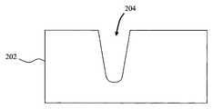
例えば、図1を参照されたい。図1に示すように、誘電体にパターニングされたときのトレンチは、丸みを帯びたトレンチ・プロファイルおよび浅い側壁角、すなわち、底部が丸み帯びたV字形プロファイルを有する。このV字形プロファイルは、導体を充填するための限られた領域しか提供しない。したがって、CVDまたはALDを使用してバリアをトレンチ内に単に堆積させた場合、この限られた領域がさらに狭くなる。図1の点線で示すように、PVDを使用して、(イオン衝撃により)トレンチを「広げ(open-up)」、台形状プロファイルを生成することができる。しかしながら、上記で強調したように、PVD層は厚すぎ、導体領域の多くを取りすぎる。 For example, see FIG. As shown in FIG. 1, the trench when patterned in dielectric has a rounded trench profile and shallow sidewall corners, ie, a V-shaped profile with a rounded bottom. This V-shaped profile provides only a limited area for conductor filling. Therefore, if CVD or ALD were used to simply deposit the barrier into the trench, this limited area would be further reduced. As shown by the dashed lines in FIG. 1, PVD can be used to “open-up” the trench (by ion bombardment) to produce a trapezoidal profile. However, as emphasized above, the PVD layer is too thick and takes up too much of the conductor area.
有利には、本明細書では、最初に厚いPVD層をトレンチ内に堆積させ、それによって領域が増加した台形状トレンチ・プロファイルを生成し、次いでPVD層を除去し、これを(薄い)CVD、ALD、またはPVDバリアで置き換えることによって、CVDまたはALDの薄膜機能とPVDのプロファイル再成形/強化機能の両方の利益を活用する技術が提供される。 Advantageously, here, we first deposit a thick PVD layer into the trench, thereby producing a trapezoidal trench profile with increased area, then remove the PVD layer, which is referred to as (thin) CVD, Replacing ALD or PVD barriers provides a technique that exploits the benefits of both the thin film capabilities of CVD or ALD and the profile reshaping/enhancement capabilities of PVD.
本発明の技術は、銅(Cu)などの従来の導体だけでなく、CoまたはRuなどの代替の導体と組み合わせて実施することができる。例えば、図2~図7の説明に関連して説明される第1の例示的な実施形態では、Co/Ru相互接続を形成するための例示的な方法論が説明される。その説明に続くのは、同じPVD、次いでCVD/ALDスキームを使用するCu相互接続の形成を含む第2の例示的な実施形態である。 The techniques of the present invention can be practiced in combination with conventional conductors such as copper (Cu) as well as alternative conductors such as Co or Ru. For example, in the first exemplary embodiment described in connection with the description of FIGS. 2-7, an exemplary methodology for forming Co/Ru interconnects is described. Following that description is a second exemplary embodiment involving the formation of a Cu interconnect using the same PVD then CVD/ALD scheme.
第1の例示的な実施形態では、図2を参照すると、プロセスは、誘電体202に少なくとも1つのトレンチ204をパターニングすることから始まる。適切な誘電体202としては、酸化シリコン(SiOx)、または有機ケイ酸塩ガラス(SiCOH)、あるいは例えば2.7未満の誘電率κを有する超低κ層間誘電体(ULK-ILD)材料、あるいはその組合せなどの酸化物材料が挙げられるが、これらに限定されない。比較すると、二酸化ケイ素(SiO2)は、誘電率κの値が3.9である。適切な超低κ誘電体材料としては、多孔質有機ケイ酸塩ガラス(pSiCOH)が挙げられるが、これに限定されない。標準的なリソグラフィおよびエッチング技術を用いて、誘電体202にトレンチ204をパターニングすることができる。単なる例として、反応性イオン・エッチング(RIE)などの指向性(すなわち異方性)エッチング・プロセスをトレンチ・エッチングに使用することができる。In a first exemplary embodiment, referring to FIG. 2, the process begins by patterning at least one
図2に示すように、パターニングされたときのトレンチ204は、丸みを帯びたトレンチ・プロファイルおよび浅い側壁角、すなわち、底部が丸みを帯びたV字形プロファイルを有し、この形状は、導体の充填に利用可能な領域を過度に制限する。トレンチ204を共形のバリアまたはバリア/湿潤層で単に裏打ちすると、この既に制限された導体領域がさらに減少する。 As shown in FIG. 2,
しかしながら、図3に示すように、PVDプロセス中のトレンチ側壁/底部に対するイオン衝撃により、トレンチ204を広げ、トレンチ204内に台形状プロファイルを生成するPVDを最初に使用して、厚い共形のライナ302をトレンチ204内に堆積させ、裏打ちする。適切なライナ302材料としては、タンタル(Ta)、窒化タンタル(TaN)、または窒化チタン(TiN)、あるいはその組合せが挙げられるが、これらに限定されない。例示的な実施形態によると、ライナ302を、約30オングストローム(Å)を超える厚さ、例えば、約35Å~約50Å、およびそれらの間の範囲の厚さに堆積させる。 However, as shown in FIG. 3, ion bombardment of the trench sidewalls/bottom during the PVD process widens the
この台形状プロファイルであっても、ライナ302の厚さは、トレンチ204の導体領域のかなりの部分を占める。したがって、PVDライナ302上に導体を充填すると、望ましくないほど高い抵抗になる。有利には、本明細書では、次にトレンチ204からPVDライナ302を選択的に除去して、台形状プロファイルを残し、その場所により薄い(PVD、ALDまたはCVD)バリア層を配置することが提案される。すなわち、トレンチ204内に台形状プロファイルを生成するためには、より厚いPVDライナ(例えば、約30Åより大きい-上記参照)の堆積が必要であるが、堆積させるPVDの層が薄いほど、トレンチ204を広げて台形プロファイルを生成するのに十分な誘電体のイオン衝撃とならない。したがって、置換バリアが薄く保たれる限り(例えば、約20Å未満-以下参照)、置換バリアを堆積させる際にPVDを用いることもできる。 Even with this trapezoidal profile, the thickness of
図4に示すように、PVDライナ302は、誘電体202に対して選択的にトレンチ204から除去される。例示的な実施形態によると、誘電体202は、SiOx、SiCOH、またはpSiCOH、あるいはその組合せなどの酸化物材料であり(上記参照)、ライナ302(例えば、Ta、TaN、またはTiN、あるいはその組合せ)は、選択的非指向性(すなわち、等方性)湿式化学エッチングなどの選択的エッチング・プロセスを使用して除去される。選択的エッチング・プロセスを使用すると、トレンチ・プロファイルがそのまま残る。したがって、残るのは、台形状プロファイルを有するトレンチ204であり、これは、パターニングされたときのトレンチ(すなわち、底部が丸みを帯びたV字形プロファイル-図2(上述)参照)のものと比較して有利には増加した導体領域を提供する。 As shown in FIG. 4,
次いで、PVD、ALDまたはCVDを使用して、薄い共形のバリア層502を(台形状)トレンチ204内に堆積させ、裏打ちする。図5を参照されたい。図5に示すように、バリア層502は、(PVDライナ302の堆積およびその後の除去から生じる)トレンチ204の台形状プロファイルと共形である。適切なバリア層502の材料には、Ta、TaN、またはTiN、あるいはその組合せが挙げられるが、これらに限定されない。例示的な実施形態によると、バリア層502を、約20Å未満、例えば、約10Å~約15Å、およびそれらの間の範囲の厚さに堆積させる。上述したように、これらの薄い厚さでは、PVDは、台形プロファイルを生成しない。バリア層502は、誘電体202内への導体(この場合、コバルト(Co)またはルテニウム(Ru)あるいはその両方)の拡散を防止する。 A thin
堆積させたときのバリア層502は、トレンチ204のみならず誘電体202の頂面上にも配置される。図5を参照されたい。しかしながら、導体の充填後に、例えば化学機械研磨(CMP)などのプロセスを使用して、オーバーバーデン(overburden)が除去され、それと共に、誘電体202の上の過剰なバリア層502が除去される。
すなわち、次に、バリア層502を覆って、(台形状)トレンチ204内に導体602を堆積させ、充填する。図6を参照されたい。適切な導体としては、CoまたはRuあるいはその両方が挙げられるが、これらに限定されない。上記で強調したように、本明細書では、銅(Cu)などのより伝統的な導体を用いた実施形態も提示される。蒸着、スパッタリング、電気化学めっきなどのプロセスを使用して、トレンチ204内に導体602を堆積させることができる。図6に示すように、堆積させると、導体602は、トレンチ204を過充填する。次いで、隣接する構造体への短絡を回避するために、このオーバーバーデンを除去する。 That is, a
例えば、図7に示すように、CMPなどのプロセスを使用して、導体602およびバリア層502を誘電体202の表面まで研磨する。その結果、導体602を誘電体202から分離する薄い(例えば、約20Å未満、例えば、約10Å~約15Å、およびそれらの間の範囲-上記参照)共形のバリア層502を有する、誘電体202に埋め込まれた台形状(CoまたはRuあるいはその両方の)相互接続702が得られる。 For example, as shown in FIG. 7, a process such as CMP is used to polish
上記で強調したように、本技術は、Cuなどの従来の導体と併せて実施することもできる。例えば、図8~図13の説明に関連して説明される別の例示的な実施形態では、Cu相互接続を形成するための例示的な方法論が説明される。 As emphasized above, the techniques can also be implemented in conjunction with conventional conductors such as Cu. For example, in another exemplary embodiment described in connection with the description of FIGS. 8-13, an exemplary methodology for forming Cu interconnects is described.
プロセスは、上記の例と同じ一般的なやり方で、誘電体202(例えば、SiOx、SiCOH、またはpSiCOH、あるいはその組合せ)に少なくとも1つのトレンチ204をパターニングすることから開始する。したがって、図8に示されるものは、図2に示されている構造体から続いており、同様の構造体は、図において同様に番号付けされている。上述したように、RIEなどのエッチング・プロセスでは、パターニングされたときのトレンチ204は、丸みを帯びたトレンチ・プロファイルおよび浅い側壁角、すなわち、底部が丸みを帯びたV字形プロファイルを有することになる。この形状は、導体の充填に利用可能な領域を過度に制限する。したがって、トレンチ204を、この場合、バリア層および湿潤層で単に裏打ちすると、この既に制限された導体領域がさらに減少する。 The process begins by patterning at least one
したがって、図8に示すように、PVDを使用して、厚い共形のライナ802をトレンチ204内に堆積させ、裏打ちする。上述したように、PVDプロセス中のトレンチ側壁/底部に対するイオン衝撃は、トレンチ204を広げ、トレンチ204内に台形状プロファイルを生成するように働く。適切なライナ802材料には、Ta、TaN、またはTiN、あるいはその組合せが挙げられるが、これらに限定されない。例示的な実施形態によると、ライナ802を、約30Åよりも大きい厚さ、例えば約35Å~約50Å、およびその間の範囲の厚さに堆積させる。 Thus, as shown in FIG. 8, PVD is used to deposit and line a thick
図8に示すように、トレンチ204は、台形状プロファイルを有する。上記で詳述したように、導体領域を増加させるためには、厚いPVDライナ802を除去する必要がある。本実施形態では、そうすることで、例えばPVD、ALDまたはCVDを使用して、薄いバリア層ならびに薄い湿潤層を配置して、Cuギャップ充填特性を高めることが可能になる。したがって、次に、PVDライナ802がトレンチ204から選択的に除去される。図9を参照されたい。 As shown in FIG. 8,
図9に示すように、PVDライナ802は、誘電体202に対して選択的にトレンチ204から除去されている。例示的な実施形態によると、誘電体202は、SiOx、SiCOH、またはpSiCOH、あるいはその組合せなどの酸化物材料であり(上記参照)、ライナ802(例えば、Ta、TaN、またはTiN、あるいはその組合せ)は、選択的非指向性(すなわち、等方性)湿式化学エッチングなどの選択的エッチング・プロセスを使用して除去される。選択的エッチング・プロセスを使用すると、トレンチ・プロファイルがそのまま残る。したがって、図9に示すように、残るのは、台形状プロファイルを有するトレンチ204であり、これは、パターニングされたときのトレンチのもの(すなわち、底部が丸みを帯びたV字形プロファイル-図2(上述)参照)と比較して有利には増加した導体領域を提供する。 As shown in FIG. 9,
次に、図10に示すように、PVD、ALDまたはCVDを使用して、薄い共形のバリア層1002を、(台形状)トレンチ204内に堆積させ、裏打ちする。バリア層1002は、(厚いPVDライナ802の堆積とその後の除去から生じる)トレンチ204の台形状プロファイルに共形である。適切なバリア層1002の材料としては、Ta、TaN、またはTiNあるいはその組合せが挙げられるが、これらに限定されない。例示的な実施形態によると、バリア層1002を、約20Å未満、例えば、約10Å~約15Å、およびそれらの間の範囲の厚さに堆積させる。上述したように、これらの薄い厚さでは、PVDは、台形プロファイルを生成しない。バリア層1002は、湿潤層材料(この場合、CoまたはRuあるいはその両方)または導体(この場合、Cu)あるいはその両方の誘電体202への拡散を防止する。 A thin
Cuのギャップ充填特性を向上させるために、次に、ALDまたはCVDを使用して、バリア層1002を覆って、(台形状)トレンチ204内に薄い共形の湿潤層1102を堆積させる。図11を参照されたい。適切な湿潤層1102の材料としては、CoまたはRuあるいはその両方が挙げられるが、これらに限定されない。Co/Ru上にCuを充填することには、顕著な利点がある。例えば、Cuは、Ruに対して優れた濡れ性を有し、Cuは、TaよりもCoをよく濡らす。例示的な実施形態によると、湿潤層1102を、約30Å未満、例えば約15Å~約20Å、およびその間の範囲の厚さに堆積させる。 To improve the gapfill properties of Cu, a thin
堆積させたときのバリア層1002および湿潤層1102は、トレンチ204内、ならびに誘電体202の上面上に配置される。図11を参照されたい。しかしながら、導体の充填に続いて、例えばCMPのようなプロセスを使用して、オーバーバーデンが除去され、それと共に、誘電体202の上の過剰なバリア層1002および湿潤層1102が除去される。
すなわち、次に、バリア層1002を覆って、湿潤層1102上で、(台形状)トレンチ204内に導体1202を堆積させ、充填する。図12を参照されたい。本例示的な実施形態では、導体1202はCuを含むが、これに限定されない。蒸着、スパッタリング、電気化学めっきなどのプロセスを使用して、トレンチ204内に導体1202を堆積させることができる。図12に示すように、堆積させると、導体1202は、トレンチ204を過充填する。次いで、隣接する構造体への短絡を回避するために、このオーバーバーデンを除去する。 That is, a
例えば、図13に示すように、CMPなどのプロセスを使用して、導体1202、バリア層1002、および湿潤層1102を誘電体202の表面まで研磨する。その結果、導体1202を誘電体202から分離する薄い(例えば、約20Å未満、例えば、約10Å~約15Å、およびそれらの間の範囲の-上記参照)共形のバリア層1002と、薄い共形の(例えば、約30Å未満、例えば、約15Å~約20Å、およびそれらの間の範囲の-上記参照)湿潤層1102と、を有する、誘電体202に埋め込まれた台形状(Cu)相互接続1302が得られる。 For example, a process such as CMP is used to polish
本技術は、以下の非限定的な例を参照することによってさらに説明される。最初に、図14に示すように、高さ対幅のアスペクト比が1.5であり、ALDバリア層の厚さが2nmの台形状トレンチ・プロファイル(「PVDプロファイル」と表示)を有する本技術を用いて形成されたCo相互接続では、底部が丸みを帯びたV字形プロファイル(「ALDプロファイル」と表示)を有する対応するトレンチと比較して、15%低いR/Cが見られる。図14では、トレンチ限界寸法(CD)(ナノメートル(nm)単位で測定)がX軸にプロットされ、ライン抵抗(オーム/マイクロメートル(Ohm/μm)単位で測定)がY軸にプロットされている。台形状トレンチ内に形成された相互接続のより低いライン抵抗は、V字形プロファイル(すなわち、パターニングされたときの)トレンチ内に形成された相互接続と比較して、導体の量が増加したことに起因する。 The technology is further described by reference to the following non-limiting examples. First, as shown in FIG. 14, the present technique has a trapezoidal trench profile (denoted “PVD profile”) with a height-to-width aspect ratio of 1.5 and an ALD barrier layer thickness of 2 nm. A 15% lower R/C is seen for Co interconnects formed using , compared to corresponding trenches having a rounded-bottom V-shaped profile (labeled "ALD profile"). In FIG. 14, trench critical dimension (CD) (measured in nanometers (nm)) is plotted on the X-axis and line resistance (measured in ohms/micrometer (Ohm/μm)) is plotted on the Y-axis. there is The lower line resistance of interconnects formed in trapezoidal trenches is attributed to the increased amount of conductor compared to interconnects formed in V-profile (i.e., when patterned) trenches. to cause.
図15は、V字形プロファイル(すなわち、パターニングされたときの)トレンチ(「ALDプロファイル」と表示)内に形成された相互接続と比較して、台形状トレンチ(「PVDプロファイル」と表示)内に形成された相互接続内の導体の量が増加したことに起因してチップ性能が向上したことを再び示す図である。すなわち、本例では、後工程(BEOL)において30nmピッチを有する本V字形プロファイルCo相互接続設計を使用して、5nmVTFETで3%の周波数性能ゲージ(FPG:Frequency Performance Gauge)の改善が示された。FPGは、チップが動作することができる最大周波数の尺度であり、すなわち、周波数が高いほど、チップはより高速/より強力になる。図15では、X軸にパワーがプロットされ、Y軸に周波数(ギガヘルツ(GHz)単位で測定)がプロットされている。 FIG. 15 shows that in trapezoidal trenches (labeled “PVD profile”) compared to interconnects formed in V-shaped (i.e., as patterned) trenches (labeled “ALD profile”). FIG. 11 again illustrates improved chip performance due to increased amount of conductors in the interconnects formed. That is, in this example, a 3% Frequency Performance Gauge (FPG) improvement was shown for a 5 nm VTFET using the present V-profile Co interconnect design with a 30 nm pitch at the back end of the line (BEOL). . FPG is a measure of the maximum frequency a chip can operate at, i.e. the higher the frequency, the faster/more powerful the chip. In FIG. 15, power is plotted on the X-axis and frequency (measured in Gigahertz (GHz)) is plotted on the Y-axis.
本発明の例示的な実施形態を本明細書で説明してきたが、本発明は、それらの正確な実施形態に限定されず、本発明の範囲から逸脱することなく当業者によって様々な他の変更および修正を行うことができることを理解されたい。 Although illustrative embodiments of the invention have been described herein, the invention is not limited to those precise embodiments, and various other modifications can be made by those skilled in the art without departing from the scope of the invention. and modifications can be made.
本明細書に記載される本発明の好ましい実施形態では、相互接続構造体を形成する方法が提供され、本方法は、誘電体に少なくとも1つのトレンチをパターニングするステップであって、パターニングされたときの少なくとも1つのトレンチが、底部が丸みを帯びたV字形プロファイルを有する、パターニングするステップと、少なくとも1つのトレンチを広げて少なくとも1つのトレンチ内に台形状プロファイルを生成するPVDを使用して、少なくとも1つのトレンチ内にライナを堆積させ、裏打ちするステップと、ライナを少なくとも1つのトレンチから誘電体に対して選択的に除去するステップであって、それによって、除去した後に、台形状プロファイルを有する少なくとも1つのトレンチが誘電体に残る、除去するステップと、PVD、ALDまたはCVDを使用して、台形状プロファイルを有する少なくとも1つのトレンチ内に共形のバリア層を堆積させ、裏打ちするステップであって、共形のバリア層が、Ta、TaN、TiN、およびそれらの組合せからなる群から選択される材料を含み、共形のバリア層が約20Å未満の厚さを有する、裏打ちするステップと、共形のバリア層を覆って、台形状プロファイルを有する少なくとも1つのトレンチ内に導体を堆積させ、充填するステップであって、導体が、Co、Ru、およびそれらの組合せからなる群から選択される、充填するステップと、導体および共形のバリア層を誘電体まで研磨するステップと、を含む。 In preferred embodiments of the invention described herein, a method of forming an interconnect structure is provided, the method comprising patterning at least one trench in a dielectric, the method comprising: at least one trench of has a V-shaped profile with a rounded bottom; depositing and lining a liner in one trench; and selectively removing the liner from the at least one trench with respect to the dielectric, thereby at least having a trapezoidal profile after removal. removing, leaving one trench in the dielectric, and depositing and lining a conformal barrier layer in at least one trench having a trapezoidal profile using PVD, ALD or CVD, wherein , the conformal barrier layer comprises a material selected from the group consisting of Ta, TaN, TiN, and combinations thereof, the conformal barrier layer having a thickness of less than about 20 Å; depositing and filling a conductor over the shaped barrier layer and into at least one trench having a trapezoidal profile, the conductor being selected from the group consisting of Co, Ru, and combinations thereof; Filling and polishing the conductor and conformal barrier layer down to the dielectric.
本明細書に記載される本発明の別の好ましい実施形態では、相互接続構造体を形成するための方法が提供され、本方法は、誘電体に少なくとも1つのトレンチをパターニングするステップであって、パターニングされたときの少なくとも1つのトレンチが、底部が丸みを帯びたV字形プロファイルを有する、パターニングするステップと、少なくとも1つのトレンチを広げて少なくとも1つのトレンチ内に台形状プロファイルを生成するPVDを使用して、少なくとも1つのトレンチ内にライナを堆積させ、裏打ちするステップと、ライナを少なくとも1つのトレンチから誘電体に対して選択的に除去するステップであって、それによって、除去した後に、台形状プロファイルを有する少なくとも1つのトレンチが誘電体に残る、除去するステップと、PVD、ALDまたはCVDを使用して、台形状プロファイルを有する少なくとも1つのトレンチ内に共形のバリア層を堆積させ、裏打ちするステップであって、共形のバリア層が、Ta、TaN、TiN、およびそれらの組合せからなる群から選択される材料を含み、共形のバリア層が約20Å未満の厚さを有する、裏打ちするステップと、ALDまたはCVDを使用して、バリア層を覆って、台形状プロファイルを有する少なくとも1つのトレンチ内に共形の湿潤層を堆積させるステップであって、共形の湿潤層が、Co、Ru、およびそれらの組合せからなる群から選択される材料を含み、共形の湿潤層が約30Å未満の厚さを有する、堆積させるステップと、共形のバリア層を覆って、共形の湿潤層上で、台形状プロファイルを有する少なくとも1つのトレンチ内に導体を堆積させ、充填するステップであって、導体がCuを含む、充填するステップと、導体および共形のバリア層を誘電体まで研磨するステップと、を含む。 In another preferred embodiment of the invention described herein, a method is provided for forming an interconnect structure, the method comprising patterning at least one trench in a dielectric, comprising: The at least one trench when patterned has a V-shaped profile with a rounded bottom, using PVD to widen the at least one trench to produce a trapezoidal profile within the at least one trench. and selectively removing the liner from the at least one trench with respect to the dielectric, thereby forming a trapezoidal shape after removal. removing, leaving at least one trench with the profile in the dielectric; and depositing and lining a conformal barrier layer in the at least one trench with the trapezoidal profile using PVD, ALD or CVD. a step wherein the conformal barrier layer comprises a material selected from the group consisting of Ta, TaN, TiN, and combinations thereof, the conformal barrier layer having a thickness of less than about 20 Å; and depositing, using ALD or CVD, a conformal wetting layer over the barrier layer and within the at least one trench having a trapezoidal profile, the conformal wetting layer comprising Co, depositing a conformal wetting layer comprising a material selected from the group consisting of Ru, and combinations thereof, wherein the conformal wetting layer has a thickness of less than about 30 Å; Depositing and filling a conductor in at least one trench having a trapezoidal profile on the layer, the filling comprising Cu, and polishing the conductor and conformal barrier layer down to the dielectric. and
Claims (20)
Translated fromJapanese誘電体に少なくとも1つのトレンチをパターニングするステップであり、パターニングされたときの前記少なくとも1つのトレンチが、底部が丸みを帯びたV字形プロファイルを有する、前記パターニングするステップと、
前記少なくとも1つのトレンチを広げて前記少なくとも1つのトレンチ内に台形状プロファイルを生成する物理的気相堆積(PVD)を使用して、前記少なくとも1つのトレンチ内にライナを堆積させ、裏打ちするステップと、
前記ライナを前記少なくとも1つのトレンチから前記誘電体に対して選択的に除去するステップであって、それによって、除去した後に、前記台形状プロファイルを有する前記少なくとも1つのトレンチが前記誘電体に残る、前記除去するステップと、
前記台形状プロファイルを有する前記少なくとも1つのトレンチ内に共形のバリア層を堆積させ、裏打ちするステップと、
前記共形のバリア層を覆って、前記台形状プロファイルを有する前記少なくとも1つのトレンチ内に導体を堆積させ、充填するステップと、
前記導体および前記共形のバリア層を前記誘電体まで研磨するステップと、
を含む、方法。A method for forming an interconnect structure, comprising:
patterning at least one trench in a dielectric, wherein the at least one trench when patterned has a V-shaped profile with a rounded bottom;
depositing and lining a liner within the at least one trench using physical vapor deposition (PVD) that widens the at least one trench to produce a trapezoidal profile within the at least one trench; ,
selectively removing the liner from the at least one trench with respect to the dielectric, thereby leaving the at least one trench having the trapezoidal profile in the dielectric after removal; the removing step;
depositing and lining a conformal barrier layer in said at least one trench having said trapezoidal profile;
depositing and filling a conductor over the conformal barrier layer and within the at least one trench having the trapezoidal profile;
polishing the conductor and the conformal barrier layer to the dielectric;
A method, including
台形状プロファイルを有する、誘電体にパターニングされた少なくとも1つのトレンチと、
前記台形状プロファイルを有する前記少なくとも1つのトレンチを裏打ちする共形のバリア層であり、Ta、TaN、TiN、およびそれらの組合せからなる群から選択される材料を含み、20Å未満の厚さを有する、前記共形のバリア層と、
前記台形状プロファイルを有する前記少なくとも1つのトレンチ内に、前記共形のバリア層を覆って配置された導体と、
含む、相互接続構造体。an interconnect structure,
at least one trench patterned in the dielectric having a trapezoidal profile;
a conformal barrier layer lining said at least one trench having said trapezoidal profile, comprising a material selected from the group consisting of Ta, TaN, TiN, and combinations thereof, and having a thickness of less than 20 Å. , the conformal barrier layer;
a conductor disposed over the conformal barrier layer in the at least one trench having the trapezoidal profile;
An interconnect structure, including
Applications Claiming Priority (3)
| Application Number | Priority Date | Filing Date | Title |
|---|---|---|---|
| US16/573,225 | 2019-09-17 | ||
| US16/573,225US11177162B2 (en) | 2019-09-17 | 2019-09-17 | Trapezoidal interconnect at tight BEOL pitch |
| PCT/IB2020/057667WO2021053419A1 (en) | 2019-09-17 | 2020-08-14 | Trapezoidal interconnect at tight beol pitch |
Publications (2)
| Publication Number | Publication Date |
|---|---|
| JP2022548081Atrue JP2022548081A (en) | 2022-11-16 |
| JP7546660B2 JP7546660B2 (en) | 2024-09-06 |
Family
ID=74869772
Family Applications (1)
| Application Number | Title | Priority Date | Filing Date |
|---|---|---|---|
| JP2022516311AActiveJP7546660B2 (en) | 2019-09-17 | 2020-08-14 | Trapezoidal interconnects at tight BEOL pitch - Patents.com |
Country Status (6)
| Country | Link |
|---|---|
| US (2) | US11177162B2 (en) |
| JP (1) | JP7546660B2 (en) |
| CN (1) | CN114127912B (en) |
| DE (1) | DE112020003469B4 (en) |
| GB (1) | GB2603346B (en) |
| WO (1) | WO2021053419A1 (en) |
Families Citing this family (1)
| Publication number | Priority date | Publication date | Assignee | Title |
|---|---|---|---|---|
| US20240339400A1 (en)* | 2023-04-10 | 2024-10-10 | Nanya Technology Corporation | Semiconductor device with filling layer and method for fabricating the same |
Family Cites Families (37)
| Publication number | Priority date | Publication date | Assignee | Title |
|---|---|---|---|---|
| US5684331A (en) | 1995-06-07 | 1997-11-04 | Lg Semicon Co., Ltd. | Multilayered interconnection of semiconductor device |
| KR100385227B1 (en)* | 2001-02-12 | 2003-05-27 | 삼성전자주식회사 | Semiconductor device having copper multy later circuit line and method of making the same |
| US7494894B2 (en)* | 2002-08-29 | 2009-02-24 | Micron Technology, Inc. | Protection in integrated circuits |
| JP4081751B2 (en) | 2002-12-11 | 2008-04-30 | ソニー株式会社 | Wiring structure manufacturing method |
| US6875693B1 (en)* | 2003-03-26 | 2005-04-05 | Lsi Logic Corporation | Via and metal line interface capable of reducing the incidence of electro-migration induced voids |
| US20040259375A1 (en)* | 2003-06-17 | 2004-12-23 | Derderian Garo J. | Removal of metal oxidation |
| US7098128B2 (en)* | 2004-09-01 | 2006-08-29 | Micron Technology, Inc. | Method for filling electrically different features |
| US8404594B2 (en) | 2005-05-27 | 2013-03-26 | Freescale Semiconductor, Inc. | Reverse ALD |
| KR100707803B1 (en) | 2005-10-28 | 2007-04-17 | 주식회사 하이닉스반도체 | Method for manufacturing a semiconductor device having a recess gate |
| US20080132050A1 (en) | 2006-12-05 | 2008-06-05 | Lavoie Adrien R | Deposition process for graded cobalt barrier layers |
| US8481423B2 (en) | 2007-09-19 | 2013-07-09 | International Business Machines Corporation | Methods to mitigate plasma damage in organosilicate dielectrics |
| US7928569B2 (en)* | 2008-08-14 | 2011-04-19 | International Business Machines Corporation | Redundant barrier structure for interconnect and wiring applications, design structure and method of manufacture |
| US8431486B2 (en) | 2010-08-10 | 2013-04-30 | International Business Machines Corporation | Interconnect structure for improved time dependent dielectric breakdown |
| US8823166B2 (en) | 2010-08-30 | 2014-09-02 | Taiwan Semiconductor Manufacturing Company, Ltd. | Pillar bumps and process for making same |
| US8525232B2 (en)* | 2011-08-10 | 2013-09-03 | International Business Machines Corporation | Semiconductor structure having a wetting layer |
| CN102332426A (en)* | 2011-09-23 | 2012-01-25 | 复旦大学 | A kind of preparation method of copper diffusion barrier layer for nanometer integrated circuit |
| US8608973B1 (en) | 2012-06-01 | 2013-12-17 | Lam Research Corporation | Layer-layer etch of non volatile materials using plasma |
| US9514983B2 (en) | 2012-12-28 | 2016-12-06 | Intel Corporation | Cobalt based interconnects and methods of fabrication thereof |
| US10032712B2 (en) | 2013-03-15 | 2018-07-24 | Taiwan Semiconductor Manufacturing Company Limited | Semiconductor structure |
| US8877633B2 (en)* | 2013-03-28 | 2014-11-04 | Globalfoundries Inc. | Methods of forming a barrier system containing an alloy of metals introduced into the barrier system, and an integrated circuit product containing such a barrier system |
| US9768220B2 (en)* | 2014-04-15 | 2017-09-19 | Taiwan Semiconductor Manufacturing Co., Ltd. | Deep trench isolation structure for image sensors |
| US9496402B2 (en)* | 2014-10-17 | 2016-11-15 | Taiwan Semiconductor Manufacturing Company, Ltd. | Metal gate with silicon sidewall spacers |
| US9768060B2 (en) | 2014-10-29 | 2017-09-19 | Applied Materials, Inc. | Systems and methods for electrochemical deposition on a workpiece including removing contamination from seed layer surface prior to ECD |
| US20160309596A1 (en) | 2015-04-15 | 2016-10-20 | Applied Materials, Inc. | Methods for forming cobalt interconnects |
| US9559107B2 (en)* | 2015-05-20 | 2017-01-31 | International Businesss Machines Corporation | Structure and method for BEOL nanoscale damascene sidewall-defined non-volatile memory element |
| US9536832B1 (en) | 2015-12-30 | 2017-01-03 | International Business Machines Corporation | Junctionless back end of the line via contact |
| US9502350B1 (en) | 2016-01-28 | 2016-11-22 | International Business Machines Corporation | Interconnect scaling method including forming dielectric layer over subtractively etched first conductive layer and forming second conductive material on dielectric layer |
| US10446496B2 (en)* | 2016-02-17 | 2019-10-15 | International Business Machines Corporation | Self-forming barrier for cobalt interconnects |
| US9984923B2 (en) | 2016-06-30 | 2018-05-29 | International Business Machines Corporation | Barrier layers in trenches and vias |
| KR102772148B1 (en) | 2016-10-02 | 2025-02-27 | 어플라이드 머티어리얼스, 인코포레이티드 | Doped selective metal caps to improve copper electromigration with ruthenium liner |
| US10090247B1 (en)* | 2017-05-03 | 2018-10-02 | International Business Machines Corporation | Semiconductor device formed by wet etch removal of Ru selective to other metals |
| US10847463B2 (en)* | 2017-08-22 | 2020-11-24 | Applied Materials, Inc. | Seed layers for copper interconnects |
| US10580696B1 (en)* | 2018-08-21 | 2020-03-03 | Globalfoundries Inc. | Interconnects formed by a metal displacement reaction |
| US20200168450A1 (en)* | 2018-11-28 | 2020-05-28 | United Microelectronics Corp. | Method for fabricating interconnect of semiconductor device |
| CN109616650A (en)* | 2018-12-10 | 2019-04-12 | 清华-伯克利深圳学院筹备办公室 | A kind of negative electrode material, its preparation method and the sodium ion battery using the same and its application |
| CN109671665B (en) | 2018-12-21 | 2021-03-26 | 上海集成电路研发中心有限公司 | Manufacturing method of groove and manufacturing method of shallow groove isolation structure |
| US11101169B2 (en)* | 2019-01-10 | 2021-08-24 | Globalfoundries U.S. Inc. | Interconnect structures with airgaps arranged between capped interconnects |
- 2019
- 2019-09-17USUS16/573,225patent/US11177162B2/enactiveActive
- 2020
- 2020-08-14WOPCT/IB2020/057667patent/WO2021053419A1/ennot_activeCeased
- 2020-08-14DEDE112020003469.0Tpatent/DE112020003469B4/enactiveActive
- 2020-08-14CNCN202080050904.9Apatent/CN114127912B/enactiveActive
- 2020-08-14GBGB2204025.7Apatent/GB2603346B/enactiveActive
- 2020-08-14JPJP2022516311Apatent/JP7546660B2/enactiveActive
- 2021
- 2021-09-23USUS17/483,330patent/US20220013406A1/ennot_activeAbandoned
Also Published As
| Publication number | Publication date |
|---|---|
| US20220013406A1 (en) | 2022-01-13 |
| GB2603346B (en) | 2023-12-20 |
| DE112020003469B4 (en) | 2024-10-10 |
| US11177162B2 (en) | 2021-11-16 |
| CN114127912B (en) | 2025-09-16 |
| DE112020003469T5 (en) | 2022-04-14 |
| GB2603346A (en) | 2022-08-03 |
| WO2021053419A1 (en) | 2021-03-25 |
| JP7546660B2 (en) | 2024-09-06 |
| US20210082744A1 (en) | 2021-03-18 |
| CN114127912A (en) | 2022-03-01 |
| GB202204025D0 (en) | 2022-05-04 |
Similar Documents
| Publication | Publication Date | Title |
|---|---|---|
| US10804199B2 (en) | Self-aligned chamferless interconnect structures of semiconductor devices | |
| JP7492618B2 (en) | Method for fabricating an integrated circuit having dual metal power rails - Patent 7523636 | |
| US20090020883A1 (en) | Semiconductor device and method for fabricating semiconductor device | |
| KR102274848B1 (en) | Barrier layer removal method and semiconductor structure forming method | |
| KR102696330B1 (en) | Metal hard masks for reducing line bending | |
| JP2022548849A (en) | Encapsulated Topography Aided Self-Aligned MRAM Top Contact | |
| US10818589B2 (en) | Metal interconnect structures with self-forming sidewall barrier layer | |
| JP7546660B2 (en) | Trapezoidal interconnects at tight BEOL pitch - Patents.com | |
| US7964497B2 (en) | Structure to facilitate plating into high aspect ratio vias | |
| US10825720B2 (en) | Single trench damascene interconnect using TiN HMO | |
| US20220028797A1 (en) | Bottom Barrier Free Interconnects Without Voids | |
| JP2002299343A (en) | Method of manufacturing semiconductor device | |
| JP2005038999A (en) | Method of manufacturing semiconductor device | |
| WO2023024869A1 (en) | Semiconductor surface planarization method, manufactured semiconductor and use | |
| KR100645207B1 (en) | Wiring Formation Method of Semiconductor Device | |
| KR101138113B1 (en) | Method for Forming Metal-Line of Semiconductor Device | |
| US6417106B1 (en) | Underlayer liner for copper damascene in low k dielectric | |
| JP2010165760A (en) | Semiconductor device and method for manufacturing the semiconductor device | |
| JP4540504B2 (en) | Manufacturing method of semiconductor device | |
| US11270910B2 (en) | Interconnect structure with partial sidewall liner | |
| US11557482B2 (en) | Electrode with alloy interface | |
| CN102446811A (en) | Metal interconnection structure and method for forming metal interlayer via holes and interconnection metal lines | |
| US10832945B2 (en) | Techniques to improve critical dimension width and depth uniformity between features with different layout densities | |
| TWI621234B (en) | Method of forming interconnect structure | |
| KR20070052452A (en) | Method for manufacturing metal wiring of semiconductor device |
Legal Events
| Date | Code | Title | Description |
|---|---|---|---|
| RD04 | Notification of resignation of power of attorney | Free format text:JAPANESE INTERMEDIATE CODE: A7424 Effective date:20220518 | |
| A621 | Written request for application examination | Free format text:JAPANESE INTERMEDIATE CODE: A621 Effective date:20230120 | |
| A977 | Report on retrieval | Free format text:JAPANESE INTERMEDIATE CODE: A971007 Effective date:20240216 | |
| A131 | Notification of reasons for refusal | Free format text:JAPANESE INTERMEDIATE CODE: A131 Effective date:20240305 | |
| A521 | Request for written amendment filed | Free format text:JAPANESE INTERMEDIATE CODE: A523 Effective date:20240528 | |
| TRDD | Decision of grant or rejection written | ||
| A01 | Written decision to grant a patent or to grant a registration (utility model) | Free format text:JAPANESE INTERMEDIATE CODE: A01 Effective date:20240806 | |
| A61 | First payment of annual fees (during grant procedure) | Free format text:JAPANESE INTERMEDIATE CODE: A61 Effective date:20240827 | |
| R150 | Certificate of patent or registration of utility model | Ref document number:7546660 Country of ref document:JP Free format text:JAPANESE INTERMEDIATE CODE: R150 |