JP2022532251A - Electropermanent magnet array - Google Patents
Electropermanent magnet arrayDownload PDFInfo
- Publication number
- JP2022532251A JP2022532251AJP2021568621AJP2021568621AJP2022532251AJP 2022532251 AJP2022532251 AJP 2022532251AJP 2021568621 AJP2021568621 AJP 2021568621AJP 2021568621 AJP2021568621 AJP 2021568621AJP 2022532251 AJP2022532251 AJP 2022532251A
- Authority
- JP
- Japan
- Prior art keywords
- permanent
- electropermanent magnet
- electromagnets
- electropermanent
- magnetic
- Prior art date
- Legal status (The legal status is an assumption and is not a legal conclusion. Google has not performed a legal analysis and makes no representation as to the accuracy of the status listed.)
- Pending
Links
Images


Classifications
- H—ELECTRICITY
- H01—ELECTRIC ELEMENTS
- H01F—MAGNETS; INDUCTANCES; TRANSFORMERS; SELECTION OF MATERIALS FOR THEIR MAGNETIC PROPERTIES
- H01F7/00—Magnets
- H01F7/02—Permanent magnets [PM]
- H—ELECTRICITY
- H01—ELECTRIC ELEMENTS
- H01F—MAGNETS; INDUCTANCES; TRANSFORMERS; SELECTION OF MATERIALS FOR THEIR MAGNETIC PROPERTIES
- H01F7/00—Magnets
- H—ELECTRICITY
- H01—ELECTRIC ELEMENTS
- H01F—MAGNETS; INDUCTANCES; TRANSFORMERS; SELECTION OF MATERIALS FOR THEIR MAGNETIC PROPERTIES
- H01F7/00—Magnets
- H01F7/06—Electromagnets; Actuators including electromagnets
- H01F7/064—Circuit arrangements for actuating electromagnets
- H—ELECTRICITY
- H01—ELECTRIC ELEMENTS
- H01F—MAGNETS; INDUCTANCES; TRANSFORMERS; SELECTION OF MATERIALS FOR THEIR MAGNETIC PROPERTIES
- H01F7/00—Magnets
- H01F7/06—Electromagnets; Actuators including electromagnets
- H01F7/20—Electromagnets; Actuators including electromagnets without armatures
- B—PERFORMING OPERATIONS; TRANSPORTING
- B23—MACHINE TOOLS; METAL-WORKING NOT OTHERWISE PROVIDED FOR
- B23Q—DETAILS, COMPONENTS, OR ACCESSORIES FOR MACHINE TOOLS, e.g. ARRANGEMENTS FOR COPYING OR CONTROLLING; MACHINE TOOLS IN GENERAL CHARACTERISED BY THE CONSTRUCTION OF PARTICULAR DETAILS OR COMPONENTS; COMBINATIONS OR ASSOCIATIONS OF METAL-WORKING MACHINES, NOT DIRECTED TO A PARTICULAR RESULT
- B23Q3/00—Devices holding, supporting, or positioning work or tools, of a kind normally removable from the machine
- B23Q3/15—Devices for holding work using magnetic or electric force acting directly on the work
- H—ELECTRICITY
- H01—ELECTRIC ELEMENTS
- H01F—MAGNETS; INDUCTANCES; TRANSFORMERS; SELECTION OF MATERIALS FOR THEIR MAGNETIC PROPERTIES
- H01F27/00—Details of transformers or inductances, in general
- H01F27/28—Coils; Windings; Conductive connections
- H—ELECTRICITY
- H01—ELECTRIC ELEMENTS
- H01F—MAGNETS; INDUCTANCES; TRANSFORMERS; SELECTION OF MATERIALS FOR THEIR MAGNETIC PROPERTIES
- H01F7/00—Magnets
- H01F7/02—Permanent magnets [PM]
- H01F7/04—Means for releasing the attractive force
- H—ELECTRICITY
- H01—ELECTRIC ELEMENTS
- H01F—MAGNETS; INDUCTANCES; TRANSFORMERS; SELECTION OF MATERIALS FOR THEIR MAGNETIC PROPERTIES
- H01F7/00—Magnets
- H01F7/06—Electromagnets; Actuators including electromagnets
- H—ELECTRICITY
- H04—ELECTRIC COMMUNICATION TECHNIQUE
- H04R—LOUDSPEAKERS, MICROPHONES, GRAMOPHONE PICK-UPS OR LIKE ACOUSTIC ELECTROMECHANICAL TRANSDUCERS; DEAF-AID SETS; PUBLIC ADDRESS SYSTEMS
- H04R9/00—Transducers of moving-coil, moving-strip, or moving-wire type
- H04R9/02—Details
- H04R9/025—Magnetic circuit
- H—ELECTRICITY
- H04—ELECTRIC COMMUNICATION TECHNIQUE
- H04R—LOUDSPEAKERS, MICROPHONES, GRAMOPHONE PICK-UPS OR LIKE ACOUSTIC ELECTROMECHANICAL TRANSDUCERS; DEAF-AID SETS; PUBLIC ADDRESS SYSTEMS
- H04R9/00—Transducers of moving-coil, moving-strip, or moving-wire type
- H04R9/02—Details
- H04R9/04—Construction, mounting, or centering of coil
- H04R9/046—Construction
Landscapes
- Physics & Mathematics (AREA)
- Electromagnetism (AREA)
- Engineering & Computer Science (AREA)
- Power Engineering (AREA)
- Magnetic Treatment Devices (AREA)
- Electromagnets (AREA)
- Prostheses (AREA)
Abstract
Translated fromJapaneseDescription
Translated fromJapanese本出願は、2019年5月17日に出願された「永久電磁石」と題された米国特許仮出願62/849,204(整理番号ASP0011PV)からの優先権を主張し、これはあらゆる目的のために参照により本明細書に組み込まれる。 This application claims priority from US patent provisional application 62 / 849,204 (reference number ASP0011PV) entitled "Electropermanent Magnets" filed May 17, 2019, for all purposes. Incorporated herein by reference to.
本出願は、永久電磁石に関連する装置及び方法を対象としている。特に、本出願は、プログラム可能な永久電磁石アレイを用いて鉄対象物を引き付けるための装置及び方法に向けられている。 This application is intended for devices and methods related to electropermanent magnets. In particular, the present application is directed to devices and methods for attracting iron objects using programmable permanent electromagnet arrays.
磁石は、磁場を生成する材料又は物体である。この磁場は目に見えないが、磁石の最も顕著な特性、つまり鉄などの他の強磁性体を引っ張る力を担う。永久磁石は、磁化されて独自の持続磁場を生成する、磁気的に硬い材料でできた物体である。磁化できる材料は、磁石に強く引き付けられる材料でもあり、強磁性と呼ばれる。これらには、鉄、ニッケル、コバルトの元素、希土類金属のいくつかの合金、及びロードストーンなどのいくつかの天然ミネラルが含まれる。強磁性体は、一般に磁性があると見なされるほど強く磁石に引き付けられる唯一の材料であるが、他のすべての物質は、いくつかの他のタイプの磁性の1つによって磁場に対して弱く反応する。 A magnet is a material or object that produces a magnetic field. This magnetic field is invisible, but it is responsible for the most striking property of magnets: the forces that pull other ferromagnets such as iron. Permanent magnets are objects made of magnetically hard materials that are magnetized to generate their own sustained magnetic field. A material that can be magnetized is also a material that is strongly attracted to magnets and is called ferromagnetism. These include elements of iron, nickel and cobalt, some alloys of rare earth metals, and some natural minerals such as lodestone. Ferromagnets are the only material that is attracted to magnets so strongly that they are generally considered to be magnetic, but all other materials react weakly to magnetic fields by one of several other types of magnetism. do.
強磁性体は、磁化できるが磁化されたままになる傾向がない焼きなまし鉄のような磁気的に「柔らかい」材料と、磁化されたままになる傾向がある磁気的に「硬い」材料に分けることができる。永久磁石は、アルニコ、アルミニウム、ニッケル、コバルト合金、ネオジムと他の希土類材料の合金、フェライトなどの「硬い」強磁性材料から作られており、それらは、製造中に強い磁場で特別な処理を受けて、内部の微結晶構造を整列させ、消磁を非常に困難にする。飽和した磁石を消磁するには、特定の磁場を印加する必要がある。この閾値は、それぞれの材料の保磁力に依存する。「硬い」材料は保磁力が高く、「柔らかい」材料は保磁力が低くなる。磁石の全体的な強度は、そのBH製品によって測定される。材料の局所的な磁化の強さは、その磁化性によって測定される。 Ferromagnets are divided into magnetically "soft" materials such as annealed iron that can be magnetized but do not tend to remain magnetized, and magnetically "hard" materials that tend to remain magnetized. Can be done. Permanent magnets are made from "hard" ferromagnetic materials such as alnico, aluminum, nickel, cobalt alloys, alloys of neodym and other rare earth materials, ferrite, etc., which are specially treated with strong magnetic fields during manufacturing. In response, it aligns the microcrystal structure inside and makes demagnetization very difficult. To degauss a saturated magnet, a specific magnetic field needs to be applied. This threshold depends on the coercive force of each material. "Hard" materials have a high coercive force, and "soft" materials have a low coercive force. The overall strength of the magnet is measured by its BH product. The strength of the local magnetization of a material is measured by its magnetization.
電磁石は、電流が流れると磁石として機能し、電流が止まると磁石ではなくなるワイヤのコイルでできている。コイルは軟鋼などの「柔らかい」強磁性体のコアの周りに巻かれていることが多く、それによって、コイルが生成する磁場を著しく高める。 An electromagnet is made of a coil of wire that functions as a magnet when an electric current flows and is no longer a magnet when the electric current stops. The coil is often wound around a core of "soft" ferromagnets such as mild steel, thereby significantly increasing the magnetic field generated by the coil.
本出願は、先行技術の不利な点を解決することを目的としている。本出願の実施例によれば、永久電磁石アレイを提供することができる。永久電磁石アレイは、平行に配置された共通の長さの複数の永久電磁石と、複数の永久電磁石の第1の端部に結合された平面磁極片とを含む。各永久電磁石は、第1の端部と第1の端部の反対側の第2の端部とを含む。 This application aims to resolve the disadvantages of the prior art. According to the embodiments of the present application, an electropermanent magnet array can be provided. The permanent electromagnet array includes a plurality of permanent electromagnets of a common length arranged in parallel and a planar magnetic pole piece coupled to the first end of the plurality of permanent electromagnets. Each permanent electromagnet includes a first end and a second end opposite the first end.
本出願の別の実施例によれば、永久電磁石アレイを提供することができる。永久電磁石アレイは、複数の磁極片と、共通の長さの複数の永久電磁石とを含む。各永久電磁石は、第1及び第2の端部を含み、永久電磁石は、一対の磁極片の間に端から端まで直線的に配置され、一対の磁極片に結合されている。 According to another embodiment of the present application, an electropermanent magnet array can be provided. The permanent electromagnet array includes a plurality of magnetic pole pieces and a plurality of permanent electromagnets of a common length. Each permanent electromagnet includes a first and second end portion, and the permanent electromagnet is arranged linearly from end to end between a pair of magnetic pole pieces and coupled to the pair of magnetic pole pieces.
本出願のさらに別の実施例によれば、装置が提供され得る。この装置は、電流パルスを提供するように構成された電気永久コイル、エネルギー貯蔵装置、電気永久コイル及びエネルギー貯蔵装置に結合されたHブリッジ駆動回路、及びスイッチング要素に結合された制御回路のうちの1つ又は複数を含む。Hブリッジドライバ回路は、エネルギー貯蔵装置から電流パルスを受信し、電気永久コイルに対して第1の方向又は第1の方向とは反対の第2の方向に電流パルスを選択的に駆動するように構成された絶縁ゲートサイリスタを含むスイッチング素子を含む。制御回路は、第1及び第2の方向を選択するように構成される。各スイッチング素子のゲート駆動電圧は、制御回路とスイッチング素子の間で光学的に絶縁されている。 According to yet another embodiment of the present application, the device may be provided. This device is among an electric permanent coil configured to provide a current pulse, an energy storage device, an H-bridge drive circuit coupled to the electric permanent coil and energy storage device, and a control circuit coupled to a switching element. Includes one or more. The H-bridge driver circuit receives the current pulse from the energy storage device and selectively drives the current pulse in the first direction or the second direction opposite to the first direction with respect to the electric permanent coil. Includes switching elements including configured isolated gate thyristors. The control circuit is configured to select the first and second directions. The gate drive voltage of each switching element is optically isolated between the control circuit and the switching element.
本出願の永久電磁石アレイは、以下に詳細に説明されており、3つの別個の状態で使用することができる。 The electropermanent magnet array of the present application is described in detail below and can be used in three separate states.
消磁-永久電磁石を消磁することにより、永久電磁石アレイをオフにすることができる。その結果、磁極がまったくなくなる。北も南もないし、引力や反発力もまったくない。 Degaussing-By degaussing the electropermanent magnets, the electropermanent magnet array can be turned off. As a result, there are no magnetic poles at all. There is neither north nor south, and there is no gravitational or repulsive force.
短距離、高グリップ力-この構成では、すべての磁束力線が、対象物の強磁性体を通り、反対の極性の隣接する極まで、短く集中した経路をたどる。磁束のほとんどすべてが対象物材料を通すため、グリップ力を最大化できる。 Short Range, High Grip Force-In this configuration, all flux lines follow a short, concentrated path through the ferromagnet of the object to adjacent poles of opposite polarity. Since almost all of the magnetic flux passes through the object material, the grip force can be maximized.
より長距離、より低いグリップ力-同様の極のアレイ(例えば、北-北-北など)は、磁力線がたどる集中的な「短絡」を作成しないため、従来の棒磁石と同様に、外に出て周りに長い経路を取る。力線は領域に集中していないため、長距離で対象物を流れることができる磁束の量は、全磁束の一部であるが、短距離構成よりもはるかに遠くまで到達する可能性があるため、遠距離で対象物に影響を及ぼし始める。 Longer distances, lower grip forces-an array of similar poles (eg, north-north-north, etc.) do not create a concentrated "short circuit" that the lines of magnetic force follow, so they are as outward as a conventional bar magnet. Go out and take a long route around. Since the field lines are not concentrated in the area, the amount of magnetic flux that can flow through the object over long distances is part of the total magnetic flux, but can reach much farther than in short distance configurations. Therefore, it begins to affect the object at a long distance.
短距離と長距離の引力モードを切り替えることができる永久電磁石が必要である。さらに、永久電磁石アレイは、以下に説明するように、現在の最先端技術に比べて多くの利点を有する。 A permanent electromagnet capable of switching between short-distance and long-distance gravitational modes is required. In addition, the electropermanent magnet array has many advantages over current state-of-the-art techniques, as described below.
第一に、2つ以上の永久電磁石を、1つの磁極片と磁石の組み合わせの体積で組み合わせることができる。この2倍の磁束密度の利点は、永久電磁石アレイのサイズが大きくなっても維持される。永久電磁石アレイは、単独の永久電磁石に比べて、体積及び重量単位当たり増大された総引力をもたらす。分極された永久電磁石と鉄表面との間の引力は、磁石と鉄表面を共に引き付けるように作用する。 First, two or more electropermanent magnets can be combined in the volume of one magnetic pole piece and magnet combination. This double magnetic flux density advantage is maintained as the size of the electropermanent magnet array increases. The electropermanent magnet array provides increased total gravitational force per volume and weight unit compared to a single electropermanent magnet. The attractive force between the polarized permanent electromagnet and the iron surface acts to attract both the magnet and the iron surface.
第二に、永久電磁石アレイは、アレイ内の1つ又は複数の永久電磁石の極性を変えることによって、短距離引力のために最適化されることと遠距離引力のために最適化されることとの間でシフトするように電気的に切り替えられ得る。永久電磁石の分極は、N極とS極によって定義され、磁束はS極からN極に進む。 Second, the electropermanent array is optimized for short-range and long-range attraction by changing the polarity of one or more electromagnets in the array. Can be electrically switched to shift between. The polarization of the electropermanent magnet is defined by the north and south poles, and the magnetic flux travels from the south pole to the north pole.
第三に、永久電磁石アレイは、総引力を直線的に増加させることができる任意のスケールで製造することができる。 Third, the electropermanent magnet array can be manufactured on any scale that can linearly increase the total gravitational force.
第四に、開示された永久電磁石アレイが一次元又は二次元で拡張するときでさえ、アレイアセンブリは、引力の方向に追加の厚さを必要としない。したがって、3次元で同時にスケーリングする必要がある次の図2Aから2Gに示すような劣った方法よりも、重量とサイズを節約できる。 Fourth, the array assembly does not require additional thickness in the direction of gravitational force, even when the disclosed electropermanent magnet array expands in one or two dimensions. Therefore, weight and size can be saved compared to the inferior method shown in FIGS. 2A to 2G below, which requires simultaneous scaling in three dimensions.
第五に、永久電磁石アレイは、個々の永久電磁石と同じ有益な特性を引き続き示す。a)2つの磁気構成のいずれかで分極することができ、b)それらは完全に消磁され、引き付けられた鉄の塊が永久電磁石アレイから分離して自由に動くことができ、c)永久電磁石の分極状態は、最初の分極パルス又は消磁パルスを超えて追加の電流を必要とせずに維持することができる。 Fifth, the electropermanent magnet array continues to exhibit the same beneficial properties as the individual electropermanent magnets. a) It can be polarized in one of two magnetic configurations, b) they are completely degaussed, and the attracted iron mass can separate from the permanent electromagnet array and move freely, c) the permanent electromagnet. The polarization state of can be maintained beyond the initial polarization pulse or degauss pulse without the need for additional current.
その他の利点と差別化は、次の図と付随する説明に示される。 Other benefits and differentiation are shown in the following figure and accompanying explanations.
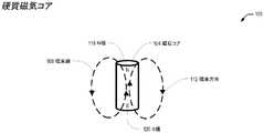
ここで図1Aを参照すると、従来技術による硬質磁気コア100を示す図が示されている。図1Aは、アルニコを含む磁気的に硬い材料と、ネオジム又はサマリウムコバルトを含む希土類の組み合わせから作製された円筒形の磁石コア104の斜視図を示している。磁石は、磁気電荷で分極された磁気的に硬い磁石コアある。磁石コア108は、必ずしも円筒形である必要はないが、本出願における一貫性のために、一般に、円筒形コアとして示されている。例えば、磁気コア104はまた、多くの可能なプリズム形状であり得る。磁石コア104は、図6Dに示されるような磁気特性を有する。 Here, with reference to FIG. 1A, a diagram showing a rigid
磁化された磁石コア104は、N極116及びS極120を有し、関連する磁場を有する。磁場は、磁力線とも呼ばれる磁束線108を使用して視覚化することができる。磁束線108は磁束の経路を示す。磁束は、表面を通過する磁束又は磁力線108の正味の数である。つまり、一方向に通過する数から反対方向に通過する数を引いた数である。関連する図では、明確にするために、各磁場に対して1つの磁束線108のみが示されている。任意の数の磁束線108が実際に存在する可能性があり、単一の磁束線108が任意の数の磁束線108を表すことができることを理解されたい。 The magnetized magnet core 104 has an
磁化された磁石コア104に関連するすべての磁束線108(磁束線108を持たない消磁された磁石コア104と比較して)は、共通の磁束方向112を有する。磁石コア104自体において、磁束方向112は、S極120からN極116に進む。磁石コア104から離れて、同じ磁束線108は、同じ磁束線108の磁束方向112が一貫しているように反対方向に進む(すなわち、時計回り又は反時計回りのいずれかの方向に示されている)。 All flux lines 108 associated with the magnetized magnet core 104 (compared to a demagnetized magnet core 104 without the flux lines 108) have a common flux direction 112. In the magnet core 104 itself, the magnetic flux direction 112 advances from the
ここで図1Bを参照すると、従来技術による、通電されたコイル巻線130を示す図が示されている。図1Bは、ワイヤ(例えば、銅線)から形成されるか、部分的な磁気ループから形成されるか(図7A~7C)、又は積み重ねられた回路基板上の導電性トレース又は相互接続されたトレースを有する層から形成される(図7D及び図7E)電気コイル134を示す。コイル134は、矢印138の方向に電流を流すプロセスでさらに示されている。当業者に知られている右手の法則によれば、図示の電流は、図示の方向112に磁束力線108を生成する。さらなる図では、矢印がコイル134に流れる電流の方向を示す場合、図に示されていない場合でも、コイル134のもう一方のリードから出る等しい電流があることを理解する必要がある。 Here, with reference to FIG. 1B, a diagram showing an energized coil winding 130 according to the prior art is shown. FIG. 1B is formed from wires (eg, copper wire), from partial magnetic loops (FIGS. 7A-7C), or conductive traces or interconnects on stacked circuit boards. FIG. 7 shows an electric coil 134 formed from a layer with traces (FIGS. 7D and 7E). Coil 134 is further illustrated in the process of passing an electric current in the direction of arrow 138. According to the right-hand rule known to those of skill in the art, the shown current produces a flux field line 108 in the direction 112 shown. In a further figure, if the arrow points in the direction of the current flowing through the coil 134, it should be understood that there is an equal current coming out of the other lead of the coil 134, even if not shown in the figure.
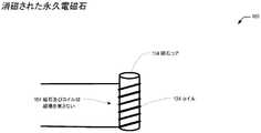
ここで図1Cを参照すると、従来技術に従って、コイル140を通る単極性電流パルスによって充電される永久電磁石を示す図が示されている。図1Cは、強力な放電パルス144及び結果として生じる磁気コア104の磁気分極によってエネルギーを与えられる電気コイル144に挿入された磁気的に硬いコア104を示している。さらに、結果として生じる分極線及び磁束線108は、電気パルス144が完了した後も残る。その結果、帯電した永久電磁石140が生じる。 Here, with reference to FIG. 1C, a diagram showing a permanent electromagnet charged by a unipolar current pulse passing through a
ここで図1Dを参照すると、従来技術に従って、コイル150を通る交流パルスによって消磁された永久電磁石を示す図が示されている。図1Dは、消磁交流パルス列154を受け取り、それによってコア104の磁気極性を消磁し、有用な磁束線をもたらさない永久電磁石を示している。 Here, with reference to FIG. 1D, a diagram showing a permanent electromagnet degaussed by an AC pulse passing through a
ここで図1Eを参照すると、従来技術に従って、コイル160内の電流によって中和された磁束を示す図が示されている。図1Eは、永久磁石の極性に正反対であるが、磁石の極性を反転させるのに十分な強度ではないコイル誘導磁束を生成する連続電流164を運ぶコイル134の内部に配置された永久磁石コア104を示している。結果として生じる永久磁石160は、電流がゼロのときに鉄材料を引き付けるであろう。ただし、図IFに示すように、磁石の磁場を打ち消すために連続電流164を印加する必要がある。最終的には、鉄の物体を放出するのに十分なゼロに近づくまで、組み合わせの正味の磁束を減らす。 Here, with reference to FIG. 1E, a diagram showing the magnetic flux neutralized by the current in the
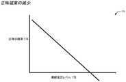
ここで図1Fを参照すると、従来技術による正味磁束170の減少を示す図が示されている。図1Fは、磁石とコイルの組み合わせ160の正味の磁束174がゼロになるまでコイル電流178を増加させることによって、永久磁石160の磁束174がどのように徐々に中和され得るかを示している。 Here, referring to FIG. 1F, a diagram showing a decrease in the net
ここで図1Gを参照すると、本出願の実施例による、180消磁された永久電磁石を示す図が示されている。図1Gは、消磁された180状態の磁石コア104及びコイル134を示している。したがって、磁石及びコイルは、磁場184を有さず、磁束線108は示されていない。この状態では、消磁された永久電磁石180-は他の物体に磁力を加えない。 Here, with reference to FIG. 1G, a diagram showing a 180 degaussed electromagnet according to an embodiment of the present application is shown. FIG. 1G shows a magnet core 104 and a coil 134 in a degaussed 180 state. Therefore, the magnet and coil do not have a magnetic field 184 and the magnetic flux lines 108 are not shown. In this state, the degaussed electromagnet 180-does not apply magnetic force to other objects.
ここで図2Aを参照すると、従来技術による単純な電磁石200を示す図が示されている。図2A~図2Hは、鉄の物体を引き付ける目的で実際に使用される従来技術の永久電磁石構成を示している。しかしながら、これらの構成はすべて、本明細書に開示される実施例よりも性能が劣っている。図2Aは、一端がコイル134に挿入された磁気的に柔らかいヨーク208を示している。この構成は、一般的な電磁石を含む。示されるように、電流が流れない場合、この電磁石は磁束を生成せず、それにより、鉄塊又は強磁性表面204への引力なしで示される。鉄塊又は強磁性表面204は、磁石に引き付けられる鉄合金から作られる。 Here, with reference to FIG. 2A, a diagram showing a
ここで図2Bを参照すると、従来技術による単純な通電電磁石220を示す図が示されている。図2Bは、磁気的に柔らかいヨーク208及び強磁性表面204を通過する電流164を示しており、これは、磁束線108が交差しなければならない2つの空隙224(明確にするために1つが示されている)を減少させる方向に引き付けられる。磁気引力の強さは、空隙が減少するにつれて増加し、電磁石220が強磁性表面204と直接接触しているときに最大になる。製品及び産業で使用されている間、電磁石220は、強磁性表面204へのその磁気的引力を維持するために、絶えず流れる電流164で電力を供給され続けなければならない。 Here, with reference to FIG. 2B, a diagram showing a simple energizing
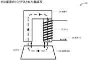
ここで図2Cを参照すると、従来技術による、ゼロ電流230のバイアスされた電磁石を示す図が示されている。図2Cは、軟鉄製の磁極片234と対にされた磁気的に帯電した永久電磁石230を示している。電流がゼロ238であっても、強磁性表面204は引き付けられる。磁極片又はヨークは、図6Eを参照して図解及び説明した磁気特性を有する磁気的に柔らかい鉄材料であり、1つ又は複数の永久電磁石の極に取り付けられて、磁束が磁気回路を流れるための低磁気抵抗経路を提供する。 Here, with reference to FIG. 2C, a diagram showing a biased electromagnet with zero current 230 according to the prior art is shown. FIG. 2C shows a magnetically charged
ここで図2Dを参照すると、従来技術に従って、磁束がキャンセルされた240のバイアスされた電磁石を示す図が示されている。図2Dは、永久磁石とは反対の磁束方向を生成する方向にコイル電流244が流れる永久電磁石240を示している。図1Fに示されている特定のレベルの電流244では、コイル134の反対の磁束が磁石の磁束を中和し、その結果、磁気の引力がなくなる。 Here, with reference to FIG. 2D, a diagram showing 240 biased electromagnets in which the magnetic flux is canceled is shown according to the prior art. FIG. 2D shows a
ここで図2Eを参照すると、従来技術による、整列された極250を有する硬磁石及び半硬磁石を示す図が示されている。図2Eは、両端234A、234Bで磁極片によって取り付けられた2つの異なる材料形式の磁石を必要とする永久電磁石構成250を示している。コイル134の内側にはアルニコ磁石254Aがあり、アルニコ磁石254Aは、左側の254Bのネオジム合金磁石よりも磁気的に硬くなく、希土類構造である可能性がある。2種類の磁石の磁気特性を図6Dに示す。図2Eに示される方向144に電流のパルスが発生すると、両方の磁石254A、254Bは一致する極性を採用し、強磁性表面204を通過する結合された磁束はそれに対応して強い。 Here, with reference to FIG. 2E, a diagram showing a hard magnet and a semi-hard magnet having aligned
ここで図2Fを参照すると、従来技術に従って、反対側の260に極を有する硬磁石及び半硬磁石を示す図が示されている。図2Fは、図2Eに示されているのと同じ永久電磁石アセンブリを示しているが、電流パルス144が反対方向に開始されている。これにより、永久電磁石の極性が反転し、左側の磁気的に硬いネオジム磁石254Bからの磁束が効果的に短絡される。空隙224を横切る磁束が残っていないので、強磁性表面204との引力はない。 Here, referring to FIG. 2F, a diagram showing a hard magnet and a semi-hard magnet having a pole on the
ここで図2Gを参照すると、従来技術に従って、電流パルス270によって充電された永久電磁石を示す図が示されている。図2Gは、強磁性表面204を引き付けるように示されている、磁気的に帯電した永久電磁石及び磁極片234を示している。これは、図3から始まる出願人の進歩性の直前に存在する最先端技術と見なされる。 Here, with reference to FIG. 2G, a diagram showing a permanent electromagnet charged by a
ここで図2Hを参照すると、従来技術に従って、交互のパルス280によって消磁された永久電磁石を示す図が示されている。図2Hは、図2Gに示されるのと同じアセンブリを示しているが、電気永久コイル134に交互の消磁パルス154が適用されており、したがって、強磁性表面204への引力を排除している。図2G及び2Hの不利な点は、磁束を強磁性表面204に効率的に伝達し、強磁性表面204を通過させるために、長い磁極片234を有する必要があることである。長い磁極片234を有することの不利な点は、磁束に対するその抵抗がわずかにあり、反対側の永久電磁石の極への磁束の漏れが大きくなり、その結果、強磁性表面204を通って移動する磁束のレベルが低くなり、そしてそれにより、表面204への磁気引力がより低いレベルになることである。長い磁極片234は、要するに、磁気引力の強さを不利に減少させ、永久電磁石設計の重量を増加させる。 Here, with reference to FIG. 2H, a diagram showing a permanent electromagnet degaussed by alternating
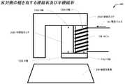
ここで図3Aを参照すると、本出願の実施例による、短距離引力300のために極性が交互になっている並んだ永久電磁石アレイを示す図が示されている。図3A~図3Eは、本出願の好ましい実施例の一形態を示している。図3Aは、共通の磁極片234を介して2部材の永久電磁石アレイ300に結合された2つの並んだ永久電磁石140A、140Bを示している。図2Gと比較して、2つの永久電磁石140A、140Bが使用されるので、磁束線の密度及び強磁性表面204への引力は、図2Gの磁石よりも約2倍大きい。この交互の磁極構成は、短距離の引力に最適化されている。すべての永久電磁石アレイにおける磁石コアから磁極片234への取り付けは、磁気引力、はんだ接着、及び接着剤接着の組み合わせた又は別個の取り付け機構によって達成することができる。 Here, with reference to FIG. 3A, a diagram showing an array of side-by-side electropermanent magnet arrays with alternating polarities for short-range
各永久電磁石は、磁気的に硬い材料部分と、硬質材料部分の周りにらせん状に巻きつけられた導電体とを含む。導電体は、ワイヤの1つと複数の積み重ねられた層とを含む。各層は、各硬質材料部分の周りで絶縁体フィルムに接合された導電性トレースの複数の平面完全ループの1つと、各硬質材料部分の周りで絶縁体フィルムに接合された導電性トレースの複数の平面及び蛇行半ループとを含む。 Each permanent electromagnet includes a magnetically hard material portion and a conductor spirally wound around the hard material portion. The conductor includes one of the wires and a plurality of stacked layers. Each layer is one of a plurality of planar perfect loops of conductive traces bonded to the insulating film around each hard material portion and a plurality of conductive traces bonded to the insulating film around each hard material portion. Includes planes and serpentine half-loops.
ここで図3Bを参照すると、図は、本出願の実施例による、より長距離の引力320のために極性が一致する、並んだ永久電磁石アレイを示している。図3Bは、図3Aと同じ並んだ永久電磁石を示しているが、ここで、永久電磁石140A、140Bは、示されている電流パルス144A、144Bによって同じSN方向に分極されている。この磁気構成では、永久電磁石アレイからの磁束線がさらに広がり、図3Aに示す交互極性の永久電磁石アレイ300構成よりも長距離で優れた引力性能を提供する。対照的に、短距離では、アレイが図3Bのように偏光している場合、磁束線は、短距離磁束と引力を低減する永久電磁石140A、140Bの本体の周りのより大きな総空隙244を通過する必要があるため、図3Aの構成よりも引力が低くなる。したがって、短距離と長距離の引力モードを切り替えることができる永久電磁石が必要である。 Referring now to FIG. 3B, the figure shows a side-by-side electropermanent magnet array with matching polarities for a
ここで図3Cを参照すると、本出願の実施例による、消磁された並んだ永久電磁石アレイ340を示す図が示されている。図3Cは、消磁電流154A、154Bを交互にすることによって消磁され、それによって、強磁性表面204と係合し、それによって強磁性表面204を引き付けない磁束線を持たない永久電磁石アレイ340をレンダリングする両方の永久電磁石140A、140Bを示す。 Here, with reference to FIG. 3C, a diagram showing a degaussed side-by-side
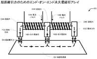
ここで図3Dを参照すると、本出願の実施例による、短距離引力350の磁束図が示されている。図3Dは、短距離、高力の引力に最適化されたN極116とS極120を交互に有する1次元の4つの永久電磁石アレイを示している。 Here, with reference to FIG. 3D, a magnetic flux diagram of a short-range
短距離引力は、本明細書では、接触から最大分離距離までの空隙224の距離で発生するものとして定義される。交互に分極された磁石の公称引力距離D2358は、磁石の中心間の距離であるD1354に等しくなる。短距離引力の最大分離距離は、距離D2358である。ここで、D2358は、永久電磁石の140中心軸間の距離D1354以下である。一実施例では、短距離引力は、接触から約0.4センチメートルまでであり得る。図示の構成では、永久電磁石アレイ350は、強磁性表面204に対して短距離の引力304を発揮する。短距離物体引力構成を達成するために、各永久電磁石140は、最も近い隣接する永久電磁石140に対して反対に帯電している。このことは、例示的な永久電磁石アレイの2×4磁石構成について図7Fにも示されている。第1列の第1、第3、第5等の磁石コア104ごと、及び第2列の第2、第4、第6等ごとの磁石コア104は、鉄対象物表面204に面するN極116で充電される。第1列の第2、第4、第6等の磁石104ごと、及び第2列の第1、第3、第5等ごとの磁石コア104は、強磁性表面204に面するS極120で充電される。磁石コア104の極性のこの交互のパターンは、対応して短い戻り経路を伴うが、最大数の磁束線108を提供し、したがって、強磁性表面204への引力範囲を制限する。磁束方向112は、S極120からN極116までであり、隣接する磁石コア104は反対に分極されているので、磁束戻り経路は非常に短い。Short-range gravitational forces are defined herein as occurring at a gap of 224 from contact to maximum separation distance. The alternately polarized magnets' nominal
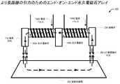
ここで図3Eを参照すると、本出願の実施例による、より長距離の引力360の磁束図が示されている。図3Eは、1次元の4つの永久電磁石アレイを示しており、並んだ各永久電磁石140は同じ分極方向を有し、より長距離の引力のために最適化されたアレイを形成している。 Here, with reference to FIG. 3E, a magnetic flux diagram of a longer distance
より長距離の引力は、本明細書では、一般に、短距離引力距離から最大分離距離までとして定義される。長い引力範囲構成の公称引力距離D2368は、永久電磁石アレイ360を横切る寸法に等しいD3364である。より長距離の引力のための最大分離距離は、距離D2368であり、D2368は、永久電磁石アレイ360を横切る寸法に等しい距離D3364以下である。一実施例では、より長距離の引力は、約0.4センチメートルから約4センチメートルまでであり得る。図示の構成では、永久電磁石アレイ360は、強磁性表面204に対してより長距離の引力308を発揮する。より長距離の物体引力構成を達成するために、各磁石104は、すぐ隣接する磁石104に同一に帯電している。これは、例示的な2×4永久電磁石アレイ300構成についても図7Gに示されている。第1列及び第2列のすべての磁石コア104は、強磁性表面204に面するN極116で充電されている。磁石コア104の電荷のこの同一のパターンは、複数の磁石コア104からの最長の磁束線108を提供し、それに対応して長い戻り経路を有する。磁束方向112は、S極120からN極116までであり、隣接する磁石コア104は同じように分極されているので、磁束戻り経路は、図3A及び図3Dの短距離引力構成の場合よりも長い。Longer gravitational forces are generally defined herein as from short range gravitational distances to maximum separation distances. The nominal
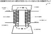
ここで図4Aを参照すると、本出願の実施例による、短距離引力400のためのエンド・オン・エンドの永久電磁石アレイを示す図が示されている。図4A~図4Eは、本出願の好ましい実施例の別の形態を示している。2つ以上の永久電磁石140は、永久電磁石140を散在させ、また各アレイの端部を覆う磁極片234で端から端まで取り付けられている。 Here, with reference to FIG. 4A, a diagram showing an end-on-end electromagnet array for a short-
図4Aは、エンド・オン・エンドの永久電磁石アレイを示している。示されているように磁石の極性が交互になっているため、永久電磁石アレイ400は、短距離での高い引力に対して最適化されている。 FIG. 4A shows an end-on-end electropermanent magnet array. Due to the alternating polarities of the magnets as shown, the
ここで図4Bを参照すると、本出願の実施例による、より長距離の引力420のためのエンド・オン・エンドの永久電磁石アレイを示す図が示されている。図4Bは、図4Aに示したものと同じエンド・オン・エンドの配置であるが、永久電磁石の極性は同じ方向に整列している。この配置では、永久電磁石アレイのより長い磁束経路長が、より長距離の引力のために最適化される。 Referring now to FIG. 4B, a diagram showing an end-on-end electromagnet array for a
ここで図4Cを参照すると、本出願の実施例による、消磁されたエンド・オン・エンドの永久電磁石アレイ440を示す図が示されている。図4Cは、強磁性表面204に引力がない、消磁状態の永久電磁石のエンド・オン・エンドの配置である。 Here, with reference to FIG. 4C, a diagram showing a degaussed end-on-end
ここで図4Dを参照すると、本出願の実施例による、短距離引力450の磁束図が示されている。図4Dは、短距離引力304のために最適化された、N極とS極が交互になっている4部材の永久電磁石アレイを示している。図4Dに示される実施例は、図3A及び図3Dに示される実施例と同じ最適化された短距離引力の目標を有するが、異なる永久電磁石140及び磁極片234構成でこれを達成する。 Here, with reference to FIG. 4D, a magnetic flux diagram of a short-range
ここで図4Eを参照すると、本出願の実施例による、より長距離の引力460の磁束図が示されている。図4Eは、示されているように、直列の磁石極性が積み重ねられた4部材の永久電磁石アレイを示している。この配置は、より長距離の引力308用に最適化されている。 Here, with reference to FIG. 4E, a magnetic flux diagram of a
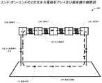
ここで図5Aを参照すると、本出願の実施例による、電流パルス・ドライバ500のブロック図が示されている。図5Aは、コマンドに応じて、電流パルスが永久電磁石のコイル524を介して前方又は後方に送られるHブリッジ電流パルス・ドライバ回路を示している。半導体スイッチのHブリッジ構成は、開いているスイッチ又は閉じているスイッチを選択することにより、負荷を介していずれかの方向に電流を流すための好ましい構成である。永久電磁石140は、磁気コア104及びコイル134を含むことが理解されるが、磁場及び極性ではなく、電流パルス生成回路をよりよく説明するために、磁石コア104は明確にするために示されていない。 Here, with reference to FIG. 5A, a block diagram of the
電流パルス・ドライバ500は、充電器508、エネルギー貯蔵装置(コンデンサ512として示される)、制御回路516、及び1つ又は複数のスイッチ(サイリスタHブリッジ504として示される)を含み得る。より多くのサイリスタHブリッジ504は、より多くのコイル524を含み得る(各コイル524は、1つの永久電磁石140に関連付けられ得る)。他の実施例では、サイリスタHブリッジ504を使用することはできず、代わりに、ハードウェアスイッチ又はアクチュエータ、MOSFET、又はIGBTを使用して、スイッチング機能を提供することができる。図5A~図5Fには1つのコイル524のみが示されているが、本出願の永久電磁石アレイは、少なくとも2つの永久電磁石、したがって少なくとも2つのコイル524を必要とすることを理解されたい。単一のコイル524は、図5A~図5Dの充電及び放電の目的に必要な構成要素を明確にするために簡単に示され、図5E及び図5Fは、永久電磁石アレイのより正確な図を表す。 The
充電器508は、制御回路516からの充電器有効化/無効化信号544によって指示されるように、コンデンサ512を充電するように機能する電源であり得る。好ましい実施例では、充電器508は、昇降圧電源などのスイッチングDC電源であり得る。他の実施例では、充電器508は、線形電源又は異なる形式のスイッチング電源を含む、異なる形態の電源であり得る。 The charger 508 can be a power source that functions to charge the
コンデンサ512は、充電器508によって所定の電圧まで充電され得る。複数のスイッチ又はサイリスタHブリッジ504を介して放電される方法は、各永久電磁石140の極性(又は、図3C及び図4Cに示されるように、消磁された永久電磁石140の場合は極性の欠如)を決定し得る。好ましい実施例では、コンデンサ512は、50uFのコンデンサであり得る。各サイリスタHブリッジ504は、1つのコイル524/(及び磁石コア104)及び4つのスイッチ528、532、536、540を含み得る。電流がコイル524を通って流れるかどうか、及び電流の進行方向を制御するために、スイッチは対で開閉され、これは永久電磁石140の極性に影響を与える。スイッチ528/540は同時に開閉でき、スイッチ532/536は同時に開閉できる。スイッチの動作は、図5B~図5Fに関してより詳細に説明されている。 The
制御回路516は、コマンド520を受け取り、それに応答して、充電器の有効化/無効化544を充電器508に制御し、制御548をスイッチ528、532、536、540のそれぞれに切り替える。コマンド520は、コンピュータ、コンピュータアプリケーション、コンピュータに関連付けられ、ユーザによって選択されたグラフィカル・ユーザ・アプリケーション(GUI)からのコマンド、又はユーザによってアクティブ化されたコントロールから出力されるハードウェアスイッチであり得る。コマンド520は、短距離引力を有効にすること、長距離引力を有効にすること、及び永久電磁石140を消磁することを含む、電流パルス・ドライバ500によって取られるいくつかのアクションを指定することができる。充電器508がコンデンサ512を充電すべき電圧レベルの指定、特定のサイリスタHブリッジ504の動作の指定、又は特定のスイッチ528、532、536、540の開位置又は閉位置の指定を含むがこれらに限定されない他のコマンド520を利用することができる。制御回路516は、プロセッサ/メモリ、マイクロコントローラ、フィールド・プログラマブル・ゲート・アレイ(FPGA)、プログラマブルロジック、ステートマシン、純粋なハードウェア、又はハードウェア/ソフトウェア/アプリケーションの任意の組み合わせを含む任意の形態の既知の制御機能として実装することができる。 The control circuit 516 receives the command 520, and in response, controls the charger enable / disable 544 to the charger 508 and switches the control 548 to each of the
別の言い方をすれば、Hブリッジ電流パルス・ドライバは、電流パルスを提供するように構成された電気永久コイル、エネルギー貯蔵装置、電気永久コイルとエネルギー貯蔵装置に結合されたHブリッジ駆動回路、及び、スイッチング素子に結合された制御回路、を含み得る。Hブリッジドライバ回路は、エネルギー貯蔵装置から電流パルスを受信し、電気永久コイルに対して第1の方向又は第1の方向とは反対の第2の方向に電流パルスを選択的に駆動するように構成された絶縁ゲートサイリスタを含むスイッチング素子を含む。制御回路は、第1及び第2の方向を選択するように構成される。各スイッチング素子のゲート駆動電圧は、制御回路とスイッチング素子の間で光学的に絶縁されている。 In other words, the H-bridge current pulse driver is an electric permanent coil configured to provide the current pulse, an energy storage device, an H-bridge drive circuit coupled to the electric permanent coil and the energy storage device, and , A control circuit coupled to a switching element, may be included. The H-bridge driver circuit receives the current pulse from the energy storage device and selectively drives the current pulse in the first direction or the second direction opposite to the first direction with respect to the electric permanent coil. Includes switching elements including configured isolated gate thyristors. The control circuit is configured to select the first and second directions. The gate drive voltage of each switching element is optically isolated between the control circuit and the switching element.
ここで図5Bを参照すると、本出願の実施例による、永久電磁石550の電流パルス・ドライバ充電段階を示すブロック図が示されている。図5Bは、蓄電コンデンサ512の充電段階におけるHブリッジ電流パルス駆動回路を示している。 Here, with reference to FIG. 5B, a block diagram showing a current pulse driver charging stage of the
充電段階550は、電流パルス・ドライバ500の動作モードを(例えば、短距離引力から長距離引力へ、又は長距離引力から短距離引力へ)変更することに関連して、又は、消磁プロセスに必要な多くの充電ステップ(図10)の1つとして使用することができる。 Charging
充電段階550の場合、制御回路516は、新しい動作モードを指定するコマンド520、又は充電コンデンサコマンド554を受信する。一実施例では、充電コンデンサコマンド554は、コンデンサ512を充電するための電圧レベルを指定することができる。次に、制御回路516は充電器556を有効にし、充電器508はコンデンサ558を充電する。一実施例では、充電器有効信号556は、コンデンサ558を所望の電圧に充電するために、制御回路516によって計時され得る。別の実施例では、充電器508は、任意の持続時間の充電器有効556表示を受信することに応答して、コンデンサ558を充電して、所望の電圧まで充電することができる。この段階では、すべてのサイリスタHブリッジ504のすべてのスイッチ528、532、536、540は、閉じたスイッチがコンデンサ512の充電を妨げる可能性があるため、開いた状態にある。 For the charging
ここで図5Cを参照すると、本出願の実施例による、コイル560を通して永久電磁石のコンデンサを順方向に放電することを示すブロック図が示されている。図5Cは、コイルの524の順方向にスイッチ1及びスイッチ4を介して電流パルスを放電するエネルギー貯蔵コンデンサ512を示している。図5C及び図5Dの放電段階は、永久電磁石アレイ300を短距離引力、長距離引力、又は消磁のためにプログラムするために、永久電磁石140が実際に分極される段階を示している。図5Cに示されている段階は、図5Bに示されている段階の後に実行される。 Here, with reference to FIG. 5C, a block diagram according to an embodiment of the present application showing a forward discharge of a capacitor of an electropermanent magnet through a
永久電磁石アレイに磁気状態をプログラムするための放電シーケンスには、次の重要な特性がある。記載された値の大きさは、設計固有の条件及び構成要素の選択に応じて変化することは、当業者には容易に明らかであるはずである。
・コンデンサの個々の放電は非常に高速なプロセスである(25マイクロ秒から100マイクロ秒の放電時間)
・コンデンサは非常に高い電流(250アンペア以上)で放電する
・非常に高い電圧(250ボルト以上)からコンデンサを放電するThe discharge sequence for programming the magnetic state in the electropermanent magnet array has the following important properties: It should be readily apparent to those of skill in the art that the magnitude of the values described will vary depending on design-specific conditions and component choices.
• Individual discharge of capacitors is a very fast process (discharge time from 25 microseconds to 100 microseconds).
-The capacitor discharges at a very high current (250 amps or more) -Discharges the capacitor from a very high voltage (250 volts or more)
永久電磁石アレイ300は、1つ又は複数のサイリスタHブリッジ504を利用して、電流の方向を制御して、永久電磁石140を所与の状態にプログラムすることができる。どのスイッチ528、532、536、及び540が開いているか、どのスイッチが閉じているかに応じて、電流は、永久電磁石コイル巻線524を通って2つの方向のうちの1つに流れ、したがって、対応する永久電磁石140(明確にするために示されていない)を2つの磁気状態(N-S又はS-N)のうちの1つにプログラムする。サイリスタ504は、MOSFET又はIGBTと比較して、それらの非常に高い電力及びエネルギー処理特性のために選択され得る。サイリスタ504が点火/トリガされると、流れがほぼゼロに低下するまで電流が流れ続けることを可能にし、これは、永久電磁石140を再プログラムするための任意の所与のコマンドに対してコンデンサ512全体が放電しなければならないことを意味する。MOSFETは大量の電力を処理できないため、タスクを実行するためにさらに多くのMOSFETが必要になる可能性がある。しかしながら、MOSFETは、サイリスタ504よりも有利に効率的であり、より制御可能である(例えば、コンデンサ512の放電は、微細な電流制御を提供するために変調され得る)。これは、単一の磁気状態を所与の永久電磁石140にプログラムすることだけを試みている永久電磁石アレイ300引力装置にとって大きな利点ではないが、永久電磁石アレイ技術が、単位電力あたりの高トルクに最適化され、適度な回転速度又は線形速度で動作するが、ゼロ速度トルクを維持するために常に通電する必要がない何らかの形の電気モータに組み込まれている場合、理論的にはより有用である可能性がある。 The
制御回路516は、コイルコマンド562を介してイネーブル順方向電流を受け取る。一実施例では、コマンド562は、スイッチ528、532、536、540のどれを開閉するかを指定することができる。別の実施例では、制御回路516は、コイルコマンド562を介してイネーブル順方向電流を受信した後、スイッチ状態528、532、536、540を決定することができる。コイルコマンド562を介してイネーブル順方向電流を受信することに応答して、制御回路516は、最初に、充電器508に充電器無効566を提供し、これにより、充電器508がコンデンサ512を充電し続けるのを停止する。一実施例では、充電器無効566は、充電器508が、おそらく1つ又は複数の電池を含む入力AC又はDC電源(図示せず)から切り離される結果となる。 The control circuit 516 receives the enable forward current via coil command 562. In one embodiment, the command 562 can specify which of the
コンデンサ512の充電を無効にした後、制御回路516は、サイリスタHブリッジ504に、スイッチSI及びS4 564を閉じるように(そして、スイッチS2 532及びS3 536を開いたままにするように)指示する。同じスイッチのアクティブ化/非アクティブ化が、永久電磁石アレイ300に存在し得る任意の他のサイリスタHブリッジ504に提供される。S1 528及びS4 540を閉じると、コンデンサ512は、両方のスイッチS1 528、S4 540を介して放電し、コイル524を通る順方向電流及び対応する永久電磁石140の磁化の変化がもたらされる。 After disabling charging of the
ここで図5Dを参照すると、本出願の実施例による、コイル570を介して逆方向に永久電磁石のコンデンサを放電することを示すブロック図が示されている。図5Dは、コイルの524の逆方向にスイッチ2及びスイッチ3を介して電流パルス578を放電するエネルギー貯蔵コンデンサ512を示している。図5C及び5Dの放電段階は、永久電磁石アレイ300を近距離引力、長距離引力、又は消磁のためにプログラムするために、永久電磁石140が実際に分極される段階を提供する。図5Dに示される段階は、図5Bに示される段階(充電コンデンサ512)の後に実行される。 Here, with reference to FIG. 5D, a block diagram according to an embodiment of the present application showing that the capacitor of the permanent electromagnet is discharged in the opposite direction via the
制御回路516は、コイルコマンド572を介してイネーブル逆電流を受け取る。一実施例では、コマンド572は、スイッチ528、532、536、540のどれを開閉するかを指定する。別の実施例では、制御回路516は、コイルコマンド572を介してイネーブル逆電流を受信した後、スイッチ状態528、532、536、540を決定する。コイルコマンド572を介してイネーブル順方向電流を受信することに応答して、制御回路516は、最初に、充電器508に充電器無効576を提供し、これは、充電器508がコンデンサ512を充電し続けるのを停止する。一実施例では、充電器無効576は、充電器508が、おそらく1つ又は複数の電池を含む入力AC又はDC電源(図示せず)から切り離される結果となる。 The control circuit 516 receives the enable reverse current via coil command 572. In one embodiment, the command 572 specifies which of the
コンデンサ512の充電を無効にした後、制御回路516は、サイリスタHブリッジ504に、スイッチS2及びS3 574を閉じるように(そして、スイッチS1 528及びS4 540を開いたままにするように)指示する。同じスイッチのアクティブ化/非アクティブ化が、電流パルス・ドライバ500に存在し得る任意の他のサイリスタHブリッジ504に提供される。S2及びS3を閉じると、コンデンサ512は、両方のスイッチS2 532、S3 536を介して放電し、コイル524を通る逆電流及び対応する永久電磁石140の磁化の変化をもたらす。 After disabling charging of the
ここで図5Eを参照すると、本出願の実施例による、複数のコイル580を備えた永久電磁石電流パルス・ドライバの第1のブロック図が示されている。複数のサイリスタHブリッジ504が存在し、本明細書では、サイリスタHブリッジA 504AからサイリスタHブリッジN 504Nまでとして識別される。各サイリスタHブリッジ504は、スイッチS1 528、S2 532、S3 536、及びS4 540を含む。サイリスタHブリッジA504Aには、スイッチS1A 528A、S2A 532A、S3A 536A、及びS4A 540Aが含まれている。サイリスタHブリッジN504Nには、スイッチS1N 528N、S2N 532N、S3N 536N、及びS4N540Nが含まれている。任意の数のサイリスタHブリッジ504が電流パルス・ドライバ500、580に存在し得、別個のスイッチ制御548が各サイリスタHブリッジ504に提供され得る。制御回路516は、スイッチ制御A 548AをサイリスタHブリッジA 504Aに提供し、スイッチ制御N 548NをサイリスタHブリッジN 504Nに提供する。 Here, with reference to FIG. 5E, a first block diagram of an electropermanent magnet current pulse driver with a plurality of
複数のサイリスタHブリッジ504が電流パルス・ドライバ580のために存在するが、スイッチ制御548は、動作モードに応じて異なる場合がある。短距離引力構成の場合、一部のコイル524は、順方向電流を使用してN極116を一方向にプログラムし得、他のコイル524は、逆電流を使用してN極116を反対方向にプログラムし得る。より長距離の引力構成の場合、すべてのコイル524は、順方向電流を使用して、N極116を同じ方向にプログラムすることができる。 Although a plurality of thyristor H-bridges 504 are present for the
ここで図5Fを参照すると、本出願の実施例による、複数のコイル584を備えた永久電磁石電流パルス・ドライバの第2のブロック図が示されている。図5Fは、複数の永久電磁石コイル524が、電気的直列又は電気的並列構成のいずれかで、又は個別に、コイル524に向けられた電流パルスを有することができるHブリッジ回路を示す。 Here, with reference to FIG. 5F, a second block diagram of an electropermanent magnet current pulse driver with a plurality of
図5Fは、複数のサイリスタHブリッジが存在する好ましい実施例を示しているが、完全なサイリスタHブリッジ504のみが必要とされる。追加の1/2サイリスタHブリッジ586は、追加のコイル524ごとに提供され得る。わかりやすくするために、コイル524Nとスイッチ532N及び540Nが含まれる最後の(N番目の)1/2サイリスタHブリッジ586のみを示している。任意の数の1/2サイリスタHブリッジ586が電流パルス・ドライバ584に存在することができ、個別のスイッチ制御548が各サイリスタHブリッジ504又は1/2サイリスタHブリッジ586に提供されることができる。制御回路516は、スイッチ制御A 548AをサイリスタHブリッジA 504Aに提供し、スイッチ制御N 548Nを1/2サイリスタHブリッジN 586に提供する。図5Fに示される実施例は、1/2サイリスタHブリッジ586のためのスイッチ528及び536を必要とせず、これは、必要とされるスイッチの数を大幅に減らす。 FIG. 5F shows a preferred embodiment in which a plurality of thyristor H-bridges are present, but only a complete thyristor H-bridge 504 is required. An additional 1/2 thyristor H-bridge 586 may be provided for each additional coil 524. For clarity, only the last (Nth) 1/2 thyristor H-bridge 586 containing the coil 524N and
永久電磁石アレイは、複数の永久電磁石に電流パルスを供給して永久電磁石を分極するように構成されたエネルギー貯蔵装置と、エネルギー貯蔵装置に結合され、永久電磁石に対して第1の方向及び第1の方向と反対の第2の方向のうちの一方に電流パルスを選択的にルーティングするように構成されたHブリッジコイル駆動回路とを含む。永久電磁石の極性は、第1の方向と第2の方向とによって決まる。一実施例では、Hブリッジコイル駆動回路は、受信された電流パルスによって、各永久電磁石を最も近い隣接する永久電磁石とは反対の方向に分極するように構成される。別の実施例では、Hブリッジコイル駆動回路は、受信された電流パルスによる最も近い隣接する永久電磁石と同じ方向に各永久電磁石を分極するように構成される。さらに別の実施例では、Hブリッジコイル駆動回路は、各永久電磁石を脱分極するように構成され、それに応じて、複数の永久電磁石は、鉄表面に引力を提供しないように構成される。 The permanent electromagnet array is coupled to an energy storage device configured to supply a current pulse to a plurality of permanent electromagnets to polarize the permanent electromagnets, and a first direction and a first direction with respect to the permanent electromagnets. Includes an H-bridge coil drive circuit configured to selectively route the current pulse in one of the second directions opposite to the direction of. The polarity of the electropermanent magnet is determined by the first direction and the second direction. In one embodiment, the H-bridge coil drive circuit is configured to polarize each permanent electromagnet in the direction opposite to the nearest adjacent permanent electromagnet by the received current pulse. In another embodiment, the H-bridge coil drive circuit is configured to polarize each permanent magnet in the same direction as the closest adjacent permanent magnet due to the received current pulse. In yet another embodiment, the H-bridge coil drive circuit is configured to depolarize each permanent electromagnet so that the plurality of permanent electromagnets do not provide attraction to the iron surface.
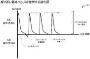
ここで図6Aを参照すると、本出願の実施例による、繰り返し電流パルス600を使用する磁化図が示されている。本出願は、単一の電流パルス144のみが永久電磁石140を磁化するために使用される実施例を含むが、実際には、3つ又は4つの単一極性電流パルス144が、通常、アレイ内の永久電磁石140を完全に分極するために使用される。図6Aは、共通の磁化方向606又は608を使用して、4つの電流パルス144が順番に使用される実施例を示している。磁化方向A606は、コイル524に対して正の方向610にコイル電流を生成する。これらの場合、4つのパルスすべてが一定期間604にわたって磁化方向A606に印加される。これらの電流602パルスのそれぞれは、レベル612に充電され、次いで、スイッチングネットワーク及びコイル524を介してコンデンサ512から放電616される。電流パルス144の間にコンデンサ充電期間614が存在する。 Here, with reference to FIG. 6A, a magnetization diagram using a repeating
ここで図6Bを参照すると、本出願の実施例による、交流単一電流パルス620を使用する消磁図が示されている。永久電磁石140を消磁するために、減少する交流パルス144を使用して、アレイ内の永久電磁石140を完全に脱分極する。脱分極とは、永久電磁石に交流電流を印加して、その磁気極性を低減又は排除することを意味する。取り付けられた鉄の塊又は強磁性表面204が解放されるように永久電磁石140を十分に脱分極するためのパルスの数は、典型的には、極性が減少する10から40の交互パルス144である。 Here, with reference to FIG. 6B, a degaussing diagram using an AC single
図示の実例では、第1の電流602パルスが、消磁方向A 624で永久電磁石140に印加され、1つ又は複数のコイル524に正の方向610でコイル電流を生成する。次に、第2の電流602パルスが消磁方向B628で永久電磁石140に印加され、負の方向630で1つ又は複数のコイル524にコイル電流を生成する。通常、この第2の電流パルス144は、同じ(負ではあるが)電流602の値を使用して印加される。次に、第1の電流パルス144よりも低い電流602の値の第3の電流パルスが、消磁方向A625で永久電磁石140に印加され、1つ又は複数のコイル524に正の方向610でコイル電流を生成する。次に、第2の電流パルス144よりも低い電流602の値の第4の電流パルスが、消磁方向B628で永久電磁石140に印加され、1つ又は複数のコイル524に負の方向630のコイル電流を生成する。交互パルスのこのシーケンスは、コイル524が消磁されるまで、電流602レベルを減少させ続ける。 In the illustrated embodiment, a first current 602 pulse is applied to the
ここで図6Cを参照すると、本出願の実施例による、例示的な磁化タイミング640を示す図が示されている。好ましい実施例では、各電流パルス144は、持続時間が約50μsのパルス幅642を有し得、パルス644の間は約50ミリ秒である。電流パルス144の振幅が減少するにつれて(図6Bによる消磁)、いくつかの実施例では、コンデンサ512を充電するために使用されるパルス644間の時間がそれに応じて減少する可能性がある。特定のパルス642及びパルス644間のタイミングは、設計に非常に依存し、回路値の関数である可能性があり、図6Cに示されているものとは異なる可能性があることを理解されたい。 Here, with reference to FIG. 6C, a diagram showing an
ここで図6Dを参照すると、本出願の実施例による、硬磁性材料及び半硬磁性材料650の両方を示す磁化図が示されている。ネオジム(NdFeB)のような磁気的に硬い材料は、AlNiCo(アルミニウム/ニッケル/コバルト)のようなわずかに硬くない材料と比較される。図6Dで、縦軸はテスラ単位の磁束密度、横軸はアンペア/メートル単位の磁場強度である。硬磁性材料は、AlNiCo(アルミニウム/ニッケル/コバルト)やネオジム(NdFeB)などの材料であり、磁気コア104材料の製造に使用される。要素がすでに低磁気抵抗回路と物理的に密接に接触している短距離引力モードなどの低磁気抵抗適用では、AlNiCoとNdFeBのグリップ力にごくわずかな違いがあるはずである。より長距離の引力の場合、ネオジム磁石のエネルギー密度が有利になる可能性がある。 Here, with reference to FIG. 6D, a magnetization diagram showing both the hard magnetic material and the semi-hard
どちらの場合も、永久電磁石コイル134、524を介して電流パルス144によって供給される印加磁気強度が正の方向に増加すると、保持磁束密度654は正の方向に増加し、電流が低下しても減少しない。逆方向電流パルス144からの印加磁場が十分に負になり、磁気コアの保持された磁場を負に反転させ、再び外部磁場が再び十分に正にパルスされるまで負のままであるまで、上記は残る。当業者が理解するように、永久電磁石コイル134、524に大電流パルス144を与えて永久電磁石140の分極を正又は負に反転させることに加えて、交流パルス144を減少させる列を適用すると、永久電磁石の磁束がゼロに減少する。 In either case, when the applied magnetic strength supplied by the current pulse 144 via the electropermanent magnet coil 134 and 524 increases in the positive direction, the holding magnetic flux density 654 increases in the positive direction, even if the current decreases. Does not decrease. The above until the applied magnetic field from the reverse current pulse 144 becomes sufficiently negative, reverses the held magnetic field of the magnetic core to negative, and remains negative until the external magnetic field is again sufficiently positively pulsed. Remains. As will be appreciated by those skilled in the art, applying a column that reduces the AC pulse 144 in addition to applying a large current pulse 144 to the electropermanent coils 134 and 524 to invert the polarization of the
ここで図6Eを参照すると、本出願の実施例による軟磁性材料670の磁化図が示されている。軟磁性材料には、鉄、コバルト、ニッケル、及びヒペルコ、パーマロイ、電磁鋼、アモルファス金属合金材料などの合金が含まれる場合がある。本明細書に記載されるように、軟磁性材料を使用して、磁極片234を製造する。図6Eは、磁気的に柔らかいヨーク208を特徴とする図2Bに示されるような包囲コイルを通って移動する電流から得られる外部から印加される磁場強度658の関数としての磁気的に柔らかい材料の磁束密度654を示す。磁気的に柔らかい材料は、磁化を保持せず、したがって、アレイ内の永久電磁石140からの磁束を効率的に空隙224に、そして強磁性表面204を通して伝導することができるので、永久電磁石アレイに使用されるすべての磁極片234に使用される。 Here, with reference to FIG. 6E, a magnetization diagram of the soft
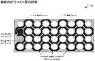
ここで図7Aを参照すると、本出願の実施例による、永久電磁石アレイ700を示す図が示されている。図7Aは、絶縁体フィルム層720上の層状蛇行導体トレース716から形成された巻線を備えた34部材の永久電磁石アレイの分解図700を示している。蛇行巻線の配置は、短距離の引力に使用される並んだ永久電磁石アレイで磁化の交互の極性パターンのみを生成するように設計されている。巻線の設計は、優れた短距離引力の目的を果たす。蛇行パターンの巻線は、導体のパッキング密度が丸線巻線で達成できるよりも高いため、アレイに並外れた磁束強度をもたらす。 Here, with reference to FIG. 7A, a diagram showing an
蛇行巻線は、絶縁膜層720上にある偶数704及び奇数708のパターン化された導体経路716を交互に配置することから製造することができる。使用実例では、電流は、端子2 732Bから最上層736のトップパッドを通って偶数層704に内向きに流れることができ、次いで、偶数層の蛇行道を移動し、次いで、奇数層708の上部端子にはんだ付けされた下部端子から出る。奇数708及び偶数704層の対及び相互接続728は、それらのはんだパッドが一緒に接続された状態で積み重ねられ続け、ある層から次の層への連続電流回路を形成する。最後に、層704、708のスタック724を通過した後、反対側の端子1 732Aが取り付けられている最下層740に到達する。最下層740は、端子1 732Aにルーティングされる。層724のスタック内の各層704、708は、通過する磁石コア104のそれぞれのための穴712を含む。 The meandering winding can be manufactured by alternately arranging even 704 and odd 708 patterned conductor paths 716 on the insulating film layer 720. In a use case, current can flow inward from terminal 2 732B through the top pad of top layer 736 to even layer 704, then travel the meandering path of even layer, and then the top of
絶縁フィルム720は、コイル層間724間の短絡を防ぐために提供される。これは、ポリアミドなどの銅メッキ薄膜プラスチックの導電性トレース716をエッチングして、所望の巻線パターンで銅コイル層を残し、ポリアミド絶縁フィルム720に密接に接合させる、可撓性プリント回路製造を使用して達成することができる。他の実施例では、他のPCB絶縁材料及び導体も可能である。開示された実施例の意図から逸脱することなく、他の形態の製造マットを使用する。一実施例では、磁石コア104は、幅約3.2mm×長さ6.4mmであり得る。ただし、最終的な要件に基づいて、任意の実用的なサイズと形状を使用できる。 The insulating film 720 is provided to prevent a short circuit between the coil layers 724. It uses a flexible printed circuit manufacturing that etches a conductive trace 716 of a copper plated thin film plastic such as polyamide, leaving a copper coil layer in the desired winding pattern and closely bonding it to the polyamide insulating film 720. Can be achieved. In other embodiments, other PCB insulating materials and conductors are also possible. Other forms of manufacturing mats are used without departing from the intent of the disclosed embodiments. In one embodiment, the magnet core 104 can be about 3.2 mm wide x 6.4 mm long. However, any practical size and shape can be used based on the final requirements.
ここで図7Bを参照すると、本出願の実施例による、均一な蛇行コイル層の詳細704を示す図が示されている。図7Bは、コイル回路層の偶数層704上の導体配線トレース716及び絶縁体720の詳細を示している。電流トレースは、上部のはんだパッド750Aから始まり、下部のはんだパッド754Aに到達するまで、それぞれが半分回転するように、連続する各磁気コア104の周りを曲がりくねっている。この電流は、アレイ内の各交流磁石コア104の周りを時計回り及び反時計回りに流れる。したがって、導通すると、電流パルス144は、続いて、交互の極性シーケンスで各磁気コア104を磁化する。蛇行回路の層を通って移動する電流は、各磁気コア104に磁束の連続する半回転758を順番に追加する。例えば、時計回りに流れる電流は、偶数層704上の磁石コア104の1つの周りを半回転し、続いて、前の層からの同じ方向の半回転の下で、時計回りの半回転方向に同じ電流を流す次の奇数層708の蛇行経路に流れる。 Here, with reference to FIG. 7B, a
ここで図7Cを参照すると、本出願の実施例による、奇数の蛇行コイル層の詳細708を示す図が示されている。図7Cは、コイル回路層の奇数層708上の導体配線トレース716及び絶縁体720の詳細を示している。奇数層708の特徴及び動作は、図7Bの偶数コイル層704に関して説明した通りであるが、代わりに、下部はんだパッド754B及び上部はんだパッド750Bを含む。 Here, with reference to FIG. 7C, a
ここで図7Dを参照すると、本出願の実施例による、スパイラル・コイル層相互接続の詳細760を示す図が示されている。図7Dは、ある層から次の層に電気的に接続された円形コイルリンクの層を示しており、円形リンク及び接続が一緒になって、磁気コア104の上下にらせん状電流経路768を形成する。実際には、スパイラル・コイル764を作成したのと同じプリント回路技術を使用して、特定のコイルを直列又は並列に接続して、一度に一緒に動作させることができる。例えば、コイル1、2、3、及び4が直列又は並列に接続され、電流144でパルスされる場合、それらは磁気コア1、2、3、及び4に1つの極性を生成する可能性がある。同様に、コイル5、6、7、及び8が電気的に直列又は並列に接続され、電流144でパルスされる場合、それらは磁気コア5、6、7、及び8に共通の極性を採用することもできる。 Here, with reference to FIG. 7D, a
実際には、コア1、2、3、及び4がコア5、6、7、及び8と反対に磁気分極されている場合、結果として得られる永久電磁石アレイは短距離引力モードにプログラムされる。このモードを図7Fに示す。さらに、コア1、2、3、及び4がコア5、6、7、及び8と同じように磁気分極されている場合、永久電磁石アレイはより長距離の引力モードにプログラムされる。このモードを図7Gに示す。 In practice, if
したがって、らせん巻き法768は、1つの永久電磁石アレイを、短距離引力又は長距離引力のいずれかのためにプログラムすることを可能にする。最後に、交流パルス144の減少するチェーンを各直列又は並列に接続されたコイル(図6B)に導入すると、アレイが消磁され、引力が生じなくなる。このモードを図7Hに示す。 Therefore, the spiral winding method 768 makes it possible to program one permanent electromagnet array for either short-range or long-range attraction. Finally, when a diminishing chain of AC pulses 144 is introduced into each coil connected in series or in parallel (FIG. 6B), the array is degaussed and no gravitational force is generated. This mode is shown in FIG. 7H.
ここで図7Eを参照すると、本出願の実施例による、スパイラル・コイル層の詳細770を示す図が示されている。図7Eは、端子1 732A及び端子2 732Bを備えた相互接続されたスパイラル・コイルを提供するために、エッチングされた導体層が別の導体層の上で相互接続されたものであることを示している。 Here, with reference to FIG. 7E, a
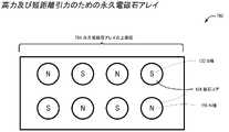
ここで図7Fを参照すると、本出願の実施例による、高力及び短距離引力780のための永久電磁石アレイの上面図を示す図が示されている。図7Fは、永久電磁石アレイ784の上面図を示している。それぞれ4つの磁石コア104の2つの列を備えた2X4の例示的な構成が示されている。高力/短距離引力構成は、反対に分極された永久電磁石140を利用して、短い磁束戻り経路を容易にする。第1又は最上列において、第1及び第3の磁石コア104は、鉄対象物表面204に面するN極116を有し、第2及び第4の磁石コア104は、鉄対象物表面204に面するS極120を有する。第2又は最下列において、第2及び第4の磁石コア104は、鉄対象物表面204に面するN極116を有し、第1及び第3の磁石コア104は、鉄対象物表面204に面するS極120を有する。 Here, with reference to FIG. 7F, a diagram showing a top view of the electropermanent magnet array for high force and
ここで図7Gを参照すると、本出願の実施例による、より低い力及びより長距離の引力786のための永久電磁石アレイの上面図を示す図が示されている。図7Gは、永久電磁石アレイ788の上面図を示している。それぞれ4つの磁石コア104の2つの列を備えた2X4の例示的な構成が示されている。より低い力/より長距離の引力構成は、同じように分極された永久電磁石140を利用して、長い磁束戻り経路を容易にする。両方の列において、すべての磁石コア104は、鉄対象物表面204に面するN極116を有する。 Here, with reference to FIG. 7G, a diagram showing a top view of the electropermanent magnet array for lower force and
ここで図7Hを参照すると、本出願の実施例による、消磁された永久電磁石アレイ790の上面図を示す図が示されている。それぞれ4つの磁石コア104の2つの列を備えた2×4の例示的な構成が示されている。図7F及び7Gに示される構成とは異なり、図1Cのすべての磁石コア104は、消磁794され、極性配向を有さない(すなわち、N極116又はS極120を有さない)。 Here, with reference to FIG. 7H, a diagram showing a top view of the degaussed
ここで図8Aを参照すると、本出願の実施例による、短距離引力800のために分極されたエンド・オン・エンドの2次元永久電磁石アレイの上面図を示す図が示されている。 Here, with reference to FIG. 8A, a diagram showing a top view of an end-on-end two-dimensional electromagnet array polarized for short-
図8Aは、8部材のエンド・オン・エンドの2次元永久電磁石アレイの上面図である。示されているアレイは、示されている南北交互のパターンで分極されており、短距離引力に対してこの構成を最適化する。この実例では、1つの永久電磁石の長さの極性変化間の距離に名目上等しい短距離。 FIG. 8A is a top view of an end-on-end two-dimensional electromagnet array of eight members. The array shown is polarized in the pattern of alternating north-south shown, optimizing this configuration for short-range attraction. In this example, a short distance that is nominally equal to the distance between polar changes in the length of one permanent electromagnet.
エンド・オン・エンド構成は、さまざまな方法で実装できることに注意されたい。これは、図4A/4Bに示すように、直線又は部分的/完全に湾曲したアレイとして、又は図8Aに示すように近接構成として実装できる。閉じた構成は、線形又は湾曲したアレイのように開始点又は終了点が定義されている必要はなく、幾何学的形状又は非幾何学的形状として実装できる。図8Aは、一対の永久電磁石140の間に磁極片234を備えた「正方形」の実施例を示している。 Note that end-on-end configurations can be implemented in different ways. This can be implemented as a linear or partially / fully curved array as shown in FIGS. 4A / 4B, or as a proximity configuration as shown in FIG. 8A. Closed configurations do not need to have a defined start or end point as in a linear or curved array and can be implemented as geometric or non-geometric shapes. FIG. 8A shows an embodiment of a "square" with a magnetic pole piece 234 between a pair of
ここで図8Bを参照すると、本出願の実施例による、エンド・オン・エンドの2次元永久電磁石アレイ及び磁束線810の側面図を示す図が示されている。図8Bは、図8Aの永久電磁石アレイ800の側面図を表す。側面からは、9つの磁極片234のうち3つだけが見え、磁極片234A、234B、及び234Cとして識別され、2つの永久電磁石140は、永久電磁石140A及び永久電磁石140Bとして識別される。各永久電磁石140は、それ自身の磁束方向112を有し、S極120からN極116に進む。 Here, with reference to FIG. 8B, a diagram showing a side view of an end-on-end two-dimensional electromagnet array and a
ここで図8Cを参照すると、本出願の実施例による、より長距離の引力820のために分極されたエンド・オン・エンドの2次元永久電磁石アレイの上面図を示す図が示されている。図8Cは、4つの永久電磁石140の2つのストリングがそれぞれ左から右に同じ方向に分極されている、エンド・オン・エンドの永久電磁石アレイ820を示している。したがって、右端の磁極片234は、アレイの最もN側のN極116であり、左端の磁極片234は、アレイの最もS側のS極120である。図8Cは、図8Dの対応するエッジビューを提供するために、45度に傾斜している。 Here, with reference to FIG. 8C, a diagram showing a top view of an end-on-end two-dimensional electromagnet array polarized for a longer
ここで図8Dを参照すると、本出願の実施例による、より長距離の引力及び磁束線830用にプログラムされたエンド・オン・エンドの2次元永久電磁石アレイの側面図を示す図が示されている。図8Dは、図8Cのエッジビューを示し、この構成を長距離引力に最適化する長い磁束線を示している。名目上、エンド・オン・エンドのマ磁石アレイのN極116とS極120の間の距離で定義される長距離。 Referring now to FIG. 8D, a diagram showing a side view of an end-on-end two-dimensional electromagnet array programmed for longer distance attraction and
実際には、永久電磁石コイルの半分は、直列又は並列の1つのグループとして電気的に接続され、残りの半分は、直列又は並列に別々に接続される。したがって、各グループは、図5A~図5Fに関して示され説明されているような電子装置である、それ自体の専用のHブリッジドライバを有することができる。Hブリッジドライバは、図6A~図6Cを参照して示し及び説明されているような、磁化及び消磁の電流パルスを供給する。この場合、巻線の2つのグループが反対方向に分極されていると、アレイは短距離の引力に最適化される。2つのグループが同じ方向に分極されると、アレイは長距離の引力に最適化される。エッジビュー830では、5つの磁極片234、磁極片234A、234B、及び234Cが見える。磁極片234の各対の間に、4つの永久電磁石140が見える。 In practice, half of the electropermanent coils are electrically connected as one group in series or in parallel, and the other half are separately connected in series or in parallel. Accordingly, each group can have its own dedicated H-bridge driver, which is an electronic device as shown and described with respect to FIGS. 5A-5F. The H-bridge driver supplies magnetized and degaussed current pulses as shown and described with reference to FIGS. 6A-6C. In this case, if the two groups of windings are polarized in opposite directions, the array is optimized for short-range attraction. When the two groups are polarized in the same direction, the array is optimized for long-range attraction. In the
ここで図9Aを参照すると、本出願の実施例による、第1のコイル磁化プロセス900を示すフローチャートが示されている。第1の実施例は、単一の充電サイクルで永久電磁石アレイを磁化し、図5A~図5Fに示される充電パルス状態を参照する。一実施例では、永久電磁石アレイは、平行に配置された共通の長さの複数の永久電磁石と、複数の永久電磁石の第1の端部に結合された平面磁極片とを含む。各永久電磁石は、第1の端部と第1の端部の反対側の第2の端部とを含む。第2の実施例では、永久電磁石アレイは、複数の磁極片と、共通の長さの複数の永久電磁石とを含む。各永久電磁石は、第1及び第2の端部を含み、永久電磁石は、一対の磁極片の間に端から端まで直線的に配置され、一対の磁極片に結合されている。フローはブロック904から始まる。 Here, with reference to FIG. 9A, a flowchart showing the first
ブロック904では、すべての永久電磁石140は既存の状態にある。既存の状態は、高力/短い引力状態、より低い力/より長い引力状態、又は消磁状態を含み得る。フローはブロック908に進む。 At block 904, all
ブロック908で、制御回路516は、(異なる)所望の磁気状態を生成するためのコマンド520を受け取る。フローはブロック912に進む。 At block 908, control circuit 516 receives a command 520 to generate a (different) desired magnetic state. The flow proceeds to block 912.
ブロック912で、制御回路516は、コマンド520からのすべてのコイル524及び永久電磁石140に必要なスイッチ状態528、532、536、540を定義する。フローは、ブロック916に進む。 At block 912, the control circuit 516 defines the switch states 528, 532, 536, 540 required for all coils 524 and
ブロック916で、制御回路516は、充電器508がコンデンサ512を充電することを可能にする。フローは、ブロック920に進む。 At block 916, the control circuit 516 allows the charger 508 to charge the
ブロック920で、充電器508はコンデンサ512を充電する。フローは決定ブロック924に進む。 At block 920, the charger 508 charges the
決定ブロック924で、制御回路516は、コンデンサ512が完全に充電されているかどうかを決定する。コンデンサ512が完全に充電されている場合、フローはブロック928に進む。コンデンサ512が完全に充電されていない場合、フローは代わりにブロック920に進み、コンデンサ512を充電し続ける。 At the determination block 924, the control circuit 516 determines whether the
ブロック928で、コンデンサ512が充電され、制御回路516が充電器508を無効にする。フローはブロック932に進む。 At block 928, the
ブロック932で、制御回路516は、スイッチ状態528、532、536、540を、ブロック912で定義された必要なスイッチ状態528、532、536、540に設定する。フローは、ブロック936に進む。 At block 932, the control circuit 516 sets the switch states 528, 532, 536, 540 to the required switch states 528, 532, 536, 540 defined in block 912. The flow proceeds to block 936.
ブロック936で、コンデンサ512は、必要なスイッチ状態528、532、536、540に対応する閉じたスイッチを通して放電する。フローは、ブロック940に進む。 At block 936, the
ブロック940で、永久電磁石アレイは、所望の磁気状態を生成する。フローはブロック940で終了する。 At block 940, the electropermanent magnet array produces the desired magnetic state. The flow ends at block 940.
ここで図9Bを参照すると、本出願の実施例による、第2のコイル磁化プロセス950を示すフローチャートが示されている。第2の実施例は、一連の充電サイクルで永久電磁石アレイを磁化する。図9Bは、必要な磁気状態が生成されるまで発生する磁化電流パルス144への蓄積コンデンサ512の繰り返しの放電を通して、永久電磁石アレイの磁化を最適化するためのプロセスを示す。この状態は、図6Aに示される4つの電流パルス144のような特定の数の磁化パルスが使用されるときである可能性がある。そうでなければ、電流パルス144は、図11A及び図11Cに示されるようなユニットからの磁束センサ出力を使用することによって測定されるように、必要な電界強度が達成されるまで継続され得る。フローはブロック954から始まる。 Here, with reference to FIG. 9B, a flowchart showing a second
ブロック954では、すべての永久電磁石140は既存の状態にある。既存の状態は、高力/短距離引力状態、低力/長距離引力状態、又は消磁状態を含み得る。フローはブロック958に進む。 At block 954, all
ブロック958で、制御回路516は、(異なる)所望の磁気状態を生成するためのコマンド520を受け取る。フローはブロック962に進む。 At block 958, control circuit 516 receives a command 520 to generate a (different) desired magnetic state. The flow proceeds to block 962.
ブロック962で、制御回路516は、コマンド520からのすべてのコイル524に必要なスイッチ状態528、532、536、540を定義する。フローは、ブロック966に進む。 At block 962, control circuit 516 defines the switch states 528, 532, 536, 540 required for all coils 524 from command 520. The flow proceeds to block 966.
ブロック966で、制御回路516は、充電器508がコンデンサ512を充電することを可能にする。フローは、ブロック970に進む。 At block 966, the control circuit 516 allows the charger 508 to charge the
ブロック970で、充電器508はコンデンサ512を充電する。図5B~図5C又は5B~図5Dによる連続する各充電サイクルは、コンデンサ512を連続的に高いレベルに充電する。永久電磁石140が完全に磁化されるまで、充電シーケンスが繰り返される。一実施例では、永久電磁石140は、永久電磁石140が所定のレベルよりも大きい引力を有する場合に、完全に磁化され得る。フローは決定ブロック974に進む。 At block 970, the charger 508 charges the
決定ブロック974で、制御回路516は、コンデンサ512が完全に充電されているかどうかを決定する。コンデンサ512が完全に充電されている場合、フローはブロック978に進む。コンデンサ512が完全に充電されていない場合、フローは代わりにブロック970に進み、コンデンサ512を充電し続ける。 At the determination block 974, the control circuit 516 determines whether the
ブロック978で、コンデンサ512が充電され、制御回路516が充電器508を無効にする。フローはブロック982に進む。 At block 978, the
ブロック982で、制御回路516は、スイッチ状態528、532、536、540を、ブロック962で定義された必要なスイッチ状態528、532、536、540に設定する。フローは、ブロック986に進む。 At block 982, the control circuit 516 sets the switch states 528, 532, 536, 540 to the required switch states 528, 532, 536, 540 defined in block 962. The flow proceeds to block 986.
ブロック986で、コンデンサ512は、必要なスイッチ状態528、532、536、540に対応する閉じたスイッチを通して放電する。フローは、決定ブロック990に進む。 At block 986, the
決定ブロック990で、制御回路516は、より多くのコンデンサ512の放電サイクルが必要かどうかを決定する。永久電磁石140がまだ完全に磁化されていない場合、又は所定の数の磁化サイクル(ブロック966~986)がまだ完了していない場合、より多くの放電サイクルが必要とされる。より多くの放電サイクルが必要な場合、フローはブロック966に進み、コンデンサ512を再び充電する。それ以上の放電サイクルが必要ない場合、フローは代わりにブロック994に進む。 At the
ブロック994で、永久電磁石アレイは、所望の磁気状態を生成する。フローはブロック994で終了する。 At block 994, the electropermanent magnet array produces the desired magnetic state. The flow ends at block 994.
ここで図10を参照すると、本出願の実施例による、コイル消磁プロセス1000を示すフローチャートが示されている。消磁プロセスは、連続的に減少する充電サイクルのシーケンスで永久電磁石アレイを非アクティブ化する。図10は、永久電磁石アレイを消磁するプロセスを示している。必要な放電サイクルの数は、10又は20などの数であり得るか、又は、図11A又は図11Cからの磁力計の読み取り値が十分に低い値に減少するためにどのくらい多くの電流パルス144が必要かに基づくことができる。フローはブロック1004から始まる。 Here, with reference to FIG. 10, a flowchart showing the
ブロック1004で、すべての永久電磁石コイル524は既存の状態にある。既存の状態は、高力/短距離引力状態又は低力/長距離引力状態を含み得る。フローはブロック1008に進む。 At block 1004, all permanent electromagnet coils 524 are in their existing state. Existing states may include high force / short range gravitational states or low force / long range gravitational states. The flow proceeds to block 1008.
ブロック1008で、制御回路516は、永久電磁石140を消磁するためのコマンド520を受け取る。フローは、ブロック1012に進む。 At block 1008, the control circuit 516 receives a command 520 to degauss the
ブロック1012で、制御回路516は、コマンド520から、すべてのコイル524について必要なコンデンサ512電圧及びスイッチ状態528、532、536、540を取得する。フローは、ブロック1016に進む。 At
ブロック1016で、制御回路516は、充電器508がコンデンサ512を充電することを可能にする。フローは、ブロック1020に進む。 At block 1016, the control circuit 516 allows the charger 508 to charge the
ブロック1020で、充電器508はコンデンサ512を充電する。図6Bによると、充電器508は、コンデンサ512を連続的に低い電圧に充電する。永久電磁石140が消磁されるまで、充電シーケンスが繰り返される。一実施例では、永久電磁石アレイが正味ゼロの引力を有する場合、永久電磁石アレイは消磁され得る。別の実施例では、永久電磁石アレイが所定のレベルの引力よりも低い場合、永久電磁石アレイを消磁することができる。フローは決定ブロック1024に進む。 At block 1020, the charger 508 charges the
決定ブロック1024で、制御回路516は、コンデンサ512が所望の電圧に到達したかどうかを決定する。消磁動作の場合、コンデンサ512は、各ステップで完全に充電されるのではなく、各充電動作又は他のすべての充電動作でより低い電圧に連続的に充電される。コンデンサ512が所望の電圧に達した場合、フローはブロック1028に進む。コンデンサ512が所望の電圧に達していない場合、フローは代わりにブロック1020に進み、コンデンサ512を充電し続ける。 At the determination block 1024, the control circuit 516 determines if the
ブロック1028で、コンデンサ512は所望の電圧に充電され、制御回路516は充電器508を無効にする。フローはブロック1032に進む。 At block 1028, the
ブロック1032で、制御回路516は、スイッチ状態528、532、536、540を、ブロック1012で定義された必要なスイッチ状態528、532、536、540に設定する。フローは、ブロック1036に進む。 At block 1032, the control circuit 516 sets the switch states 528, 532, 536, 540 to the required switch states 528, 532, 536, 540 defined in
ブロック1036で、コンデンサ512は、必要なスイッチ状態528、532、536、540に対応する閉じたスイッチを通して放電する。フローは、決定ブロック1040に進む。 At block 1036, the
決定ブロック1040で、制御回路516は、より多くの放電サイクルが必要かどうかを決定する。永久電磁石140がまだ消磁されていない場合、又は所定の数の消磁サイクル(ブロック1016-1036)がまだ完了していない場合、より多くの放電サイクルが必要とされる。それ以上の放電サイクルが必要な場合、フローはブロック1016に進み、コンデンサ512を再び充電する。それ以上の放電サイクルが必要ない場合、フローは代わりにブロック1044に進む。 At the
ブロック1044で、永久電磁石アレイが消磁され、消磁プロセスが完了する。フローはブロック1044で終了する。 At block 1044, the electropermanent magnet array is degaussed and the degaussing process is complete. The flow ends at block 1044.
ここで図11Aを参照すると、本出願の実施例による、磁力計設置1100の側面図を示す図が示されている。磁力計は、多くの場合、センサ(磁力計)1104を通って流れる磁束を測定するホール効果センサに基づいている。それは、平面磁極片234の裏側に取り付けられ、永久電磁石アレイの1つ又は複数の永久電磁石140と位置合わせされている。 Here, with reference to FIG. 11A, a diagram showing a side view of the
図11Aは、並んだ永久電磁石アレイ用の磁力計の設置を示している。この構成では、アレイの個々の永久電磁石140を出入りする磁束の一部は、例えば、個々の永久電磁石140から磁力計ヨーク1104を通って磁極片234に戻る磁束の一部を伝導するなど、磁極片234の機械加工された円形溝又は磁束迂回スロット1112によって迂回される。永久電磁石140の1つを通過する磁束の量を知ることにより、アレイ全体が強磁性表面204からほぼ同じ距離にあるときに、アレイ全体を通過する磁束を推定することができる。 FIG. 11A shows the installation of magnetometers for side-by-side electropermanent magnet arrays. In this configuration, a portion of the magnetic flux entering and exiting the
センサ1104を通って流れる磁束を測定することによって、プロセッサ又は制御回路516は、異なる機能を最適化することができる。 By measuring the magnetic flux flowing through the sensor 1104, the processor or control circuit 516 can optimize different functions.
1.通電及び放電-永久電磁石の状態を知ることによって、そして磁束を測定することによって、制御回路516は、状態変化コマンド520を達成するためにコンデンサ512に適切な充電電圧を選択することができる。これにより、消磁サイクルを実行するときに、所望の状態のオーバーシュート又はアンダーシュートを防ぐのを助けることができる。センサ1104からの信号は、制御回路516に供給されるアナログ電圧出力、無線信号、光信号などであり得る。 1. 1. By knowing the state of the energizing and discharging-electropermanent magnets, and by measuring the magnetic flux, the control circuit 516 can select the appropriate charging voltage for the
2.対象物感知-鉄対象物表面204と強く密接に接触している活性化された永久電磁石140は、回路の磁気抵抗が低いため、高い総磁束を有する可能性がある。鉄対象物204が良好に接触していないか、又は完全に存在しない場合、磁束は、磁気回路を完成させるために、高磁気抵抗の空気又は真空ギャップを介して戦わなければならず、総磁束を大幅に低下させる。したがって、永久電磁石140が作動し、測定された磁束が予想よりもはるかに低い場合、それは、強磁性表面204との良好な接触がないことの指標である可能性がある。これは、接触が良好でない可能性があることを視覚的に確認する人間のオペレータがいない可能性がある自動化されたプロセスに特に役立つ。 2. 2. Object Sensing-The activated
一実施例では、永久電磁石アレイは、複数の永久電磁石の反対側の磁極片の背面にある溝、囲まれた領域内で背面に取り付けられた磁束センサ、並びに、磁極片の反対側の磁束センサ及び溝の外側の磁極片に取り付けられた鉄製のキャップを含み得る。溝は、1つ又は複数の永久電磁石に対応する領域を囲む。1つ又は複数の永久電磁石を通って流れる磁束の一部は、磁束センサを通って流れ、それに応答して、磁束センサは、永久電磁石アレイと鉄表面との間の距離を反映する近接表示を提供するように構成される。 In one embodiment, the electropermanent magnet array is a groove on the back of the magnetic pole pieces on the opposite side of the plurality of permanent electromagnets, a magnetic flux sensor mounted on the back side in the enclosed area, and a magnetic flux sensor on the opposite side of the magnetic pole pieces. And may include an iron cap attached to a magnetic flux piece on the outside of the groove. The groove surrounds the area corresponding to one or more permanent electromagnets. A portion of the magnetic flux flowing through one or more permanent magnets flows through the flux sensor, and in response, the flux sensor provides a proximity indication that reflects the distance between the permanent electromagnet array and the iron surface. Configured to provide.
別の実施例では、永久電磁石アレイは、永久電磁石の端部と磁極片との間に取り付けられた磁束センサを含むことができる。磁束センサは、永久電磁石アレイと鉄表面との間の距離を反映する近接表示を提供するように構成されている。 In another embodiment, the electropermanent magnet array can include a magnetic flux sensor mounted between the end of the electropermanent magnet and a piece of magnetic pole. The magnetic flux sensor is configured to provide a proximity display that reflects the distance between the electropermanent magnet array and the iron surface.
ここで図11Bを参照すると、本出願の実施例による、磁力計設置1120の底面図を示す図が示されている。図11Bは、磁石112、磁力計1104、及び磁束迂回スロット1112の間の位置関係を示している。 Here, with reference to FIG. 11B, a diagram showing a bottom view of the
図11Bは、永久電磁石コア、磁力計1104、及び磁束迂回スロット1112の同軸位置決めを示す、磁力計1104の取り付けの底面図を示している。リターン・パス・ヨークはこの図には示されていないが、迂回スロット1112の直径に重なっている。 FIG. 11B shows a bottom view of the attachment of the magnetometer 1104 showing the coaxial positioning of the electropermanent magnet core, the magnetometer 1104, and the flux detour slot 1112. The return path yoke, which is not shown in this figure, overlaps the diameter of the detour slot 1112.
ここで図11Cを参照すると、本出願の実施例による、エンド・オン・エンドアレイ1130の厚さモード磁束センサの側面図を示す図が示されている。図11Cは、厚さモード磁束センサ1104を取り付けて、エンド・オン・エンド磁気アレイの1つのアームを通って流れる磁束を測定する方法を示している。磁束センサ1104は、(例えば)ホール効果又は磁束ゲート効果に基づいて、センサを通って移動する磁束に比例する電圧信号を出力する電子デバイスである。厚さモード磁束センサは、厚みを通過する磁束を測定する磁束センサである。永久電磁石アレイが鉄表面204に実質的に平行である場合、1つの磁束センサ1104の出力は、アレイ全体の磁束強度及び引力を示し得る。磁束は、永久電磁石アレイ、磁極片234、空隙224、強磁性表面204、及び厚さモード磁束センサ1104を通って移動し、磁気回路を形成する。 Here, with reference to FIG. 11C, a diagram showing a side view of the thickness mode magnetic flux sensor of the end-on-
実際には、永久電磁石アレイを備えた磁束センサ1104の使用により、ユーザは、アレイが表面に磁気的に取り付けられているか(センサ1104を通る高磁束)、又は、鉄表面204に引き付けられるが接続されていないか(中程度の磁束)、又は鉄表面204から遠く離れているか(低磁束)どうかを決定することができる。 In practice, by using a magnetic flux sensor 1104 with an electropermanent magnet array, the user can either have the array magnetically attached to the surface (high flux through the sensor 1104) or be attracted to the iron surface 204 but connected. It can be determined whether it is not (medium magnetic flux) or far from the iron surface 204 (low magnetic flux).
最後に、当業者は、本出願の同じ目的を実行するための他の構造を設計又は修正するための基礎として、添付の特許請求の範囲によって定義される出願の精神及び範囲から逸脱することなく、開示された概念及び特定の実施例を容易に使用できることを理解すべきである。 Finally, one of ordinary skill in the art will not deviate from the spirit and scope of the application as defined by the appended claims as a basis for designing or modifying other structures to carry out the same purpose of the application. It should be understood that the disclosed concepts and specific embodiments can be readily used.
本明細書の図に一般的に説明及び図示されているように、本出願の構成要素は、多種多様な異なる構成で配置及び設計され得ることが容易に理解されよう。したがって、実施形態の詳細な説明は、特許請求されるような出願の範囲を限定することを意図するものではなく、単に、出願の選択された例示的な実施例を代表するものである。 It will be readily appreciated that the components of this application may be arranged and designed in a wide variety of different configurations, as generally described and illustrated in the figures herein. Accordingly, the detailed description of the embodiments is not intended to limit the scope of the claims as claimed, but merely represent selected exemplary embodiments of the application.
当業者は、上記のような適用が、異なる順序のステップで、及び/又は具体的に開示されているものとは異なる構成のハードウェア要素で実施され得ることを容易に理解するであろう。したがって、出願はこれらの好ましい実施例に基づいて説明されてきたが、出願の精神及び範囲内にとどまりながら、特定の修正、変形、及び代替の構造が明らかであることは当業者には明らかであろう。したがって、出願の範囲と範囲を決定するために、本特許請求の範囲を参照する必要がある。 One of ordinary skill in the art will readily appreciate that applications such as those described above can be performed in different order steps and / or with hardware elements of different configurations than those specifically disclosed. Accordingly, although the application has been described on the basis of these preferred embodiments, it will be apparent to those skilled in the art that certain modifications, modifications, and alternative structures will be apparent while remaining within the spirit and scope of the application. There will be. Therefore, it is necessary to refer to the scope of the present patent claims in order to determine the scope and scope of the application.
本出願の好ましい実施例が説明されてきたが、説明された実施例は例示にすぎず、同等物及び変更(例えば、プロトコル、ハードウェアデバイス、ソフトウェアプラットフォームなど)の全範囲を考慮した場合、出願の範囲は、添付の特許請求の範囲によってのみ定義されるべきであることが理解されるべきである。 Although preferred embodiments of the present application have been described, the embodiments described are merely exemplary and, given the full scope of equivalents and modifications (eg, protocols, hardware devices, software platforms, etc.), the application. It should be understood that the scope of is to be defined only by the appended claims.
Claims (20)
Translated fromJapanese前記複数の永久電磁石の前記第1の端部に結合された平面状の磁極片と
を備える、永久電磁石アレイ。A plurality of electropermanent magnets having a common length arranged in parallel, each of which is a first end and a second end opposite to the first end. With multiple electromagnets, including parts,
An electropermanent magnet array comprising a planar magnetic pole piece coupled to the first end of the plurality of electropermanent magnets.
磁気的硬質材料部分と、
前記硬質材料部分にらせん状に巻かれた導電体と
を含み、前記導電体が、
ワイヤと、
複数の積層体層であって、各々の層が、
各々の前記硬質材料部分の周りで絶縁体フィルムに接合された導電性トレースの複数の平面状の完全ループと、
各々の前記硬質材料部分の周りで前記絶縁体フィルムに接合された導電性トレースの複数の平面状の蛇行半ループと
のうちの1つを含む、複数の積層体層と
のうちの1つを含む、請求項1に記載の永久電磁石アレイ。Each of the plurality of permanent electromagnets
With magnetic hard material parts,
The conductor includes a conductor spirally wound around the hard material portion, and the conductor is:
With wires
Multiple laminated layers, each of which
With multiple planar complete loops of conductive traces bonded to the insulating film around each said rigid material portion,
One of a plurality of laminated layers, including one of a plurality of planar meandering semi-loops of conductive traces bonded to the insulator film around each said rigid material portion. The permanent electromagnet array according to claim 1.
前記エネルギー貯蔵装置に結合されたHブリッジコイル駆動回路であって、前記永久電磁石に対して第1の方向及び前記第1の方向とは反対の第2の方向の一方に前記電流パルスを選択的にルーティングするように構成され、前記永久電磁石の極性が、前記第1及び第2の方向によって決定される、Hブリッジコイル駆動回路と
をさらに備え、
前記Hブリッジコイル駆動回路は、受信された電流パルスによって、各永久電磁石を最も近い隣接する永久電磁石とは反対の方向に分極するように構成されている、請求項1に記載の永久電磁石アレイ。An energy storage device configured to polarize the permanent electromagnets by supplying a current pulse to the plurality of permanent electromagnets.
An H-bridge coil drive circuit coupled to the energy storage device that selectively directs the current pulse in one of a first direction with respect to the electropermanent magnet and a second direction opposite to the first direction. Further comprising an H-bridge coil drive circuit configured to route to, where the polarity of the electropermanent magnet is determined by the first and second directions.
The permanent electromagnet array according to claim 1, wherein the H-bridge coil drive circuit is configured to polarize each permanent electromagnet in a direction opposite to the nearest adjacent permanent electromagnet by a received current pulse.
前記エネルギー貯蔵装置に結合されたHブリッジコイル駆動回路であって、前記永久電磁石に対して第1の方向及び前記第1の方向とは反対の第2の方向の一方に前記電流パルスを選択的にルーティングするように構成され、前記永久電磁石の極性が、前記第1及び第2の方向によって決定される、Hブリッジコイル駆動回路と
をさらに備え、
前記Hブリッジコイル駆動回路は、受信された電流パルスによって、各永久電磁石を最も近い隣接する永久電磁石と同じ方向に分極するように構成されている、請求項1に記載の永久電磁石アレイ。An energy storage device configured to polarize the permanent electromagnets by supplying a current pulse to the plurality of permanent electromagnets.
An H-bridge coil drive circuit coupled to the energy storage device that selectively directs the current pulse in one of a first direction with respect to the electropermanent magnet and a second direction opposite to the first direction. Further comprising an H-bridge coil drive circuit configured to route to, where the polarity of the electropermanent magnet is determined by the first and second directions.
The permanent electromagnet array according to claim 1, wherein the H-bridge coil drive circuit is configured to polarize each permanent electromagnet in the same direction as the nearest adjacent permanent electromagnet by a received current pulse.
前記エネルギー貯蔵装置に結合されたHブリッジコイル駆動回路であって、前記永久電磁石に対して第1の方向と前記第1の方向とは反対の第2の方向との間で前記電流パルスを交互にルーティングするように構成されたHブリッジコイル駆動回路と
をさらに備え、
前記Hブリッジコイル駆動回路は、各永久電磁石を脱分極するように構成され、それに応じて、前記複数の永久電磁石は、鉄表面に引力を提供しないように構成されている、請求項1に記載の永久電磁石アレイ。An energy storage device configured to depolarize the permanent electromagnets by providing a series of decreasing magnitude AC pulses to the plurality of permanent electromagnets.
An H-bridge coil drive circuit coupled to the energy storage device, the current pulse alternating between a first direction with respect to the electropermanent magnet and a second direction opposite to the first direction. Further equipped with an H-bridge coil drive circuit configured to route to
The H-bridge coil drive circuit is configured to depolarize each permanent electromagnet, and accordingly, the plurality of permanent electromagnets are configured not to provide an attractive force to the iron surface, according to claim 1. Electropermanent magnet array.
前記囲まれた領域内で前記背面に取り付けられた磁束センサと、
前記磁極片の反対側の前記磁束センサと前記溝の外側の前記磁極片とに取り付けられた鉄製キャップと
をさらに備え、
前記1つ又は複数の永久電磁石を通って流れる磁束の一部が前記磁束センサを通って流れ、それに応じて、前記磁束センサは、前記永久電磁石アレイと鉄表面との間の距離を反映する近接表示を提供するように構成されている、請求項1に記載の永久電磁石アレイ。A groove on the back surface of the magnetic pole piece opposite to the plurality of permanent electromagnets and surrounding a region corresponding to one or more permanent electromagnets.
With the magnetic flux sensor mounted on the back surface in the enclosed area,
Further comprising an iron cap attached to the magnetic flux sensor on the opposite side of the magnetic pole piece and the magnetic pole piece on the outside of the groove.
A portion of the magnetic flux flowing through the one or more electropermanent magnets flows through the magnetic flux sensor, and the magnetic flux sensor responds to the proximity reflecting the distance between the electropermanent magnet array and the iron surface. The electropermanent magnet array according to claim 1, which is configured to provide a display.
共通の長さの複数の永久電磁石であって、それぞれが、第1及び第2の端部を含み、一対の磁極片の間に端から端まで直線的に配置され、前記一対の磁極片に結合されている、複数の永久電磁石と
を備える、永久電磁石アレイ。With multiple magnetic pole pieces,
A plurality of permanent electromagnets of a common length, each containing a first and a second end, arranged linearly from end to end between a pair of magnetic pieces, in the pair of magnetic pieces. A permanent electromagnet array with multiple permanent electromagnets coupled.
磁気的硬質材料部分と、
前記硬質材料部分にらせん状に巻かれた導電体と
を含み、前記導電体が、
ワイヤと
複数の積層体層であって、各々の層が、
各々の前記磁気的硬質材料部分の周りで絶縁体フィルムに接合された導電性トレースの複数の平面状の完全ループを含む、複数の積層体層と
のうちの1つを含む、請求項9に記載の永久電磁石アレイ。Each of the plurality of permanent electromagnets
With magnetic hard material parts,
The conductor includes a conductor spirally wound around the hard material portion, and the conductor is:
Wires and multiple laminate layers, each layer
9. The invention comprises one of a plurality of laminated layers, comprising a plurality of planar complete loops of conductive traces bonded to an insulating film around each said magnetically rigid material portion. The electropermanent magnet array described.
前記エネルギー貯蔵装置に結合されたHブリッジコイル駆動回路であって、前記永久電磁石に対して第1の方向及び前記第1の方向とは反対の第2の方向の一方に前記電流パルスを選択的にルーティングするように構成され、前記永久電磁石の極性が、前記第1及び第2の方向によって決定される、Hブリッジコイル駆動回路と
をさらに備え、
前記Hブリッジコイル駆動回路は、受信された電流パルスによって、各永久電磁石を最も近い隣接する永久電磁石とは反対の方向に分極するように構成されている、請求項9に記載の永久電磁石アレイ。An energy storage device configured to polarize the permanent electromagnets by supplying a current pulse to the plurality of permanent electromagnets.
An H-bridge coil drive circuit coupled to the energy storage device that selectively directs the current pulse in one of a first direction with respect to the electropermanent magnet and a second direction opposite to the first direction. Further comprising an H-bridge coil drive circuit configured to route to, where the polarity of the electropermanent magnet is determined by the first and second directions.
The permanent electromagnet array according to claim 9, wherein the H-bridge coil drive circuit is configured to polarize each permanent electromagnet in a direction opposite to the nearest adjacent permanent electromagnet by a received current pulse.
前記エネルギー貯蔵装置に結合されたHブリッジコイル駆動回路であって、前記永久電磁石に対して第1の方向及び前記第1の方向とは反対の第2の方向の一方に前記電流パルスを選択的にルーティングするように構成され、前記永久電磁石の極性が、前記第1及び第2の方向によって決定される、Hブリッジコイル駆動回路と
をさらに備え、
前記Hブリッジコイル駆動回路は、受信された電流パルスによって、各永久電磁石を最も近い隣接する永久電磁石と同じ方向に分極するように構成されている、請求項9に記載の永久電磁石アレイ。An energy storage device configured to polarize the permanent electromagnets by supplying a current pulse to the plurality of permanent electromagnets.
An H-bridge coil drive circuit coupled to the energy storage device that selectively directs the current pulse in one of a first direction with respect to the electropermanent magnet and a second direction opposite to the first direction. Further comprising an H-bridge coil drive circuit configured to route to, where the polarity of the electropermanent magnet is determined by the first and second directions.
The permanent electromagnet array according to claim 9, wherein the H-bridge coil drive circuit is configured to polarize each permanent electromagnet in the same direction as the nearest adjacent permanent electromagnet by a received current pulse.
前記エネルギー貯蔵装置に結合されたHブリッジコイル駆動回路であって、前記永久電磁石に対して第1の方向と前記第1の方向とは反対の第2の方向との間で前記電流パルスを交互にルーティングするように構成されたHブリッジコイル駆動回路と
をさらに備え、
前記Hブリッジコイル駆動回路は、各永久電磁石を脱分極するように構成され、それに応じて、前記複数の永久電磁石は、鉄表面に引力を提供しないように構成されている、請求項9に記載の永久電磁石アレイ。An energy storage device configured to depolarize the permanent electromagnets by providing a series of decreasing magnitude current pulses to the plurality of permanent electromagnets.
An H-bridge coil drive circuit coupled to the energy storage device, the current pulse alternating between a first direction with respect to the electropermanent magnet and a second direction opposite to the first direction. Further equipped with an H-bridge coil drive circuit configured to route to
The H-bridge coil drive circuit is configured to depolarize each permanent electromagnet, and accordingly, the plurality of permanent electromagnets are configured not to provide an attractive force to the iron surface, according to claim 9. Electropermanent magnet array.
前記磁束センサは、前記永久電磁石アレイと鉄表面との間の距離を反映する近接表示を提供するように構成されている、請求項9に記載の永久電磁石アレイ。Further equipped with a magnetic flux sensor mounted between the end of the electropermanent magnet and the magnetic pole piece,
The permanent electromagnet array according to claim 9, wherein the magnetic flux sensor is configured to provide a proximity display that reflects the distance between the electropermanent magnet array and the iron surface.
電流パルスを提供するように構成されたエネルギー貯蔵装置と、
前記電気永久コイルと前記エネルギー貯蔵装置とに結合されたHブリッジ駆動回路であって、前記エネルギー貯蔵装置から電流パルスを受信し、前記電気永久コイルに対して第1の方向又は前記第1の方向と反対の第2の方向に前記電流パルスを選択的に駆動するように構成された絶縁ゲートサイリスタを含むスイッチング素子を含む、Hブリッジ駆動回路と、
前記スイッチング素子に結合され、前記第1及び第2の方向を選択するように構成された制御回路であって、各スイッチング素子のゲート駆動電圧が、前記制御回路と前記スイッチング素子との間で光学的に絶縁されている、制御回路と
を備える、装置。With an electric permanent coil,
With an energy storage device configured to provide current pulses,
An H-bridge drive circuit coupled to the electric permanent coil and the energy storage device, which receives a current pulse from the energy storage device and receives a current pulse from the electric permanent coil in a first direction or the first direction with respect to the electric permanent coil. An H-bridge drive circuit comprising a switching element including an isolated gate thyristor configured to selectively drive the current pulse in a second direction opposite to that of the H-bridge.
A control circuit coupled to the switching element and configured to select the first and second directions, wherein the gate drive voltage of each switching element is optical between the control circuit and the switching element. A device that is insulated from the ground and has a control circuit.
Priority Applications (1)
| Application Number | Priority Date | Filing Date | Title |
|---|---|---|---|
| JP2025004281AJP2025069180A (en) | 2019-05-17 | 2025-01-10 | Permanent Electromagnet Array |
Applications Claiming Priority (3)
| Application Number | Priority Date | Filing Date | Title |
|---|---|---|---|
| US201962849204P | 2019-05-17 | 2019-05-17 | |
| US62/849,204 | 2019-05-17 | ||
| PCT/US2020/033344WO2020236685A1 (en) | 2019-05-17 | 2020-05-18 | Electropermanent magnet array |
Related Child Applications (1)
| Application Number | Title | Priority Date | Filing Date |
|---|---|---|---|
| JP2025004281ADivisionJP2025069180A (en) | 2019-05-17 | 2025-01-10 | Permanent Electromagnet Array |
Publications (1)
| Publication Number | Publication Date |
|---|---|
| JP2022532251Atrue JP2022532251A (en) | 2022-07-13 |
Family
ID=73231578
Family Applications (2)
| Application Number | Title | Priority Date | Filing Date |
|---|---|---|---|
| JP2021568621APendingJP2022532251A (en) | 2019-05-17 | 2020-05-18 | Electropermanent magnet array |
| JP2025004281APendingJP2025069180A (en) | 2019-05-17 | 2025-01-10 | Permanent Electromagnet Array |
Family Applications After (1)
| Application Number | Title | Priority Date | Filing Date |
|---|---|---|---|
| JP2025004281APendingJP2025069180A (en) | 2019-05-17 | 2025-01-10 | Permanent Electromagnet Array |
Country Status (4)
| Country | Link |
|---|---|
| US (2) | US10984936B2 (en) |
| EP (2) | EP3973557A4 (en) |
| JP (2) | JP2022532251A (en) |
| WO (2) | WO2020236685A1 (en) |
Families Citing this family (9)
| Publication number | Priority date | Publication date | Assignee | Title |
|---|---|---|---|---|
| US9694910B2 (en) | 2013-02-22 | 2017-07-04 | World View Enterprises Inc. | Near-space operation systems |
| US9540091B1 (en) | 2016-02-11 | 2017-01-10 | World View Enterprises Inc. | High altitude balloon systems and methods |
| US10124875B1 (en) | 2017-01-09 | 2018-11-13 | World View Enterprises Inc. | Continuous multi-chamber super pressure balloon |
| US10336432B1 (en) | 2017-01-09 | 2019-07-02 | World View Enterprises Inc. | Lighter than air balloon systems and methods |
| US10984936B2 (en)* | 2019-05-17 | 2021-04-20 | Altius Space Machines Inc. | Electropermanent magnet array |
| US12202631B2 (en)* | 2021-04-19 | 2025-01-21 | Roopnarine | Servicing systems for on-orbit spacecrafts |
| WO2023115125A1 (en)* | 2021-12-21 | 2023-06-29 | Australian Native Musical Instruments Pty Ltd | A method and system for delivering a pre-selected amplified output for a stringed instrument |
| US12257695B2 (en)* | 2022-10-16 | 2025-03-25 | The Boeing Company | Pick-and-place manufacturing system and method |
| US12325504B2 (en) | 2022-11-07 | 2025-06-10 | World View Enterprises Inc. | Magnetic ballast dispenser |
Citations (9)
| Publication number | Priority date | Publication date | Assignee | Title |
|---|---|---|---|---|
| JPS5156957A (en)* | 1974-11-15 | 1976-05-19 | Hitachi Ltd | CHOKURYUYODENJIKOIRUNOSEIZOHOHO |
| DE3201826A1 (en)* | 1982-01-21 | 1983-09-08 | Hallmann, Gisela, 2000 Hamburg | Permanent-magnet retaining device which can be switched by electrical polarity reversal |
| JPS60103602A (en)* | 1983-11-10 | 1985-06-07 | Toshiba Corp | Coil |
| US5991147A (en)* | 1997-07-03 | 1999-11-23 | Chiang; Wen-Hsuan | Electromagnetic chuck with magnetizing/demagnetizing circuit |
| JP2000133512A (en)* | 1998-10-23 | 2000-05-12 | Riichi Fujii | Grid-shaped pattern coil |
| JP2012031474A (en)* | 2010-07-30 | 2012-02-16 | Tokyo Electric Power Co Inc:The | Galvanic anode for electrolytic protection |
| JP2012529181A (en)* | 2009-06-02 | 2012-11-15 | コリレイテッド マグネティックス リサーチ, エルエルシー | Magnetic field emission system and method |
| US20140049347A1 (en)* | 2012-08-16 | 2014-02-20 | DocMagnet, Inc. | Variable field magnetic holding system |
| WO2014033757A1 (en)* | 2012-08-31 | 2014-03-06 | Uttam Sarda | Electro permanent magnetic holding apparatus with magnetic flux sensor |
Family Cites Families (25)
| Publication number | Priority date | Publication date | Assignee | Title |
|---|---|---|---|---|
| US5285154A (en) | 1991-10-15 | 1994-02-08 | Eldec Corporation | Saturable core proximity sensor aligned perpendicular to a magnet target having a plate and a non-magnetic metal housing |
| US5705924A (en) | 1993-11-09 | 1998-01-06 | Eastman Kodak Company | Hall effect sensor for detecting an induced image magnet in a smooth material |
| US5986450A (en) | 1997-04-04 | 1999-11-16 | Analog Devices | Directionally independent magnet sensor |
| US7301334B2 (en) | 2001-09-17 | 2007-11-27 | Schneider Electric Industries Sas | Micro magnetic proximity sensor system |
| WO2005088259A1 (en) | 2004-03-11 | 2005-09-22 | Robert Bosch Gmbh | Magnet sensor arrangement |
| WO2007033437A1 (en)* | 2005-09-26 | 2007-03-29 | Magswitch Technology Worldwide Pty Ltd | Magnet arrays |
| US7753836B2 (en)* | 2006-06-15 | 2010-07-13 | The Trustees Of Columbia University In The City Of New York | Systems and methods for inducing electric field pulses in a body organ |
| US7846310B2 (en) | 2006-12-13 | 2010-12-07 | Applied Materials, Inc. | Encapsulated and water cooled electromagnet array |
| US8183726B2 (en)* | 2007-03-30 | 2012-05-22 | Norman Rittenhouse | Electric motor assist bicyle |
| US7960867B2 (en)* | 2007-11-27 | 2011-06-14 | Extremely Ingenious Engineering | Methods and systems for wireless energy and data transmission |
| US8373527B2 (en)* | 2008-04-04 | 2013-02-12 | Correlated Magnetics Research, Llc | Magnetic attachment system |
| CN103038982B (en)* | 2009-01-27 | 2016-08-17 | 麻省理工学院 | Motor based on electrical permanent-magnet |
| WO2010128527A2 (en)* | 2009-05-06 | 2010-11-11 | Uttam Sarda | An electro permanent magnetic work holding system involving conversion of magnetic pole from square pole to long pole or a cross pole configuration or vice versa |
| US8242649B2 (en)* | 2009-05-08 | 2012-08-14 | Fradella Richard B | Low-cost minimal-loss flywheel battery |
| JP5594184B2 (en) | 2011-02-25 | 2014-09-24 | 株式会社デンソー | Electromagnetic switch device |
| TWI415369B (en)* | 2011-06-24 | 2013-11-11 | Univ Nat Cheng Kung | Magnetization apparatus |
| US8629572B1 (en)* | 2012-10-29 | 2014-01-14 | Reed E. Phillips | Linear faraday induction generator for the generation of electrical power from ocean wave kinetic energy and arrangements thereof |
| US9620953B2 (en)* | 2013-03-25 | 2017-04-11 | Wen Technology, Inc. | Methods providing control for electro-permanent magnetic devices and related electro-permanent magnetic devices and controllers |
| US9343216B2 (en)* | 2013-09-02 | 2016-05-17 | Glen A. Robertson | Energy efficient bi-stable permanent magnet actuation system |
| US9561429B2 (en) | 2014-10-30 | 2017-02-07 | Stern Pinball, Inc. | Electromagnet for an amusement game device |
| US20170000309A1 (en) | 2016-05-31 | 2017-01-05 | Parker William Wadd | Electromagnetic Nail Sweeper |
| US10012518B2 (en) | 2016-06-08 | 2018-07-03 | Allegro Microsystems, Llc | Magnetic field sensor for sensing a proximity of an object |
| US10971292B2 (en)* | 2016-12-07 | 2021-04-06 | University Of Florida Research Foundation, Inc. | Axisymmetric electropermanent magnets |
| JP6907334B2 (en)* | 2016-12-22 | 2021-07-21 | フラクタル ブレイド, インコーポレイテッド | Equipment and methods for material manipulation |
| US10984936B2 (en)* | 2019-05-17 | 2021-04-20 | Altius Space Machines Inc. | Electropermanent magnet array |
- 2020
- 2020-05-17USUS16/876,096patent/US10984936B2/enactiveActive
- 2020-05-18JPJP2021568621Apatent/JP2022532251A/enactivePending
- 2020-05-18EPEP20810552.8Apatent/EP3973557A4/enactivePending
- 2020-05-18WOPCT/US2020/033344patent/WO2020236685A1/ennot_activeCeased
- 2021
- 2021-03-25USUS17/212,830patent/US11615904B2/enactiveActive
- 2021-03-30EPEP21933457.0Apatent/EP4315373A4/enactivePending
- 2021-03-30WOPCT/US2021/024887patent/WO2022203693A1/ennot_activeCeased
- 2025
- 2025-01-10JPJP2025004281Apatent/JP2025069180A/enactivePending
Patent Citations (9)
| Publication number | Priority date | Publication date | Assignee | Title |
|---|---|---|---|---|
| JPS5156957A (en)* | 1974-11-15 | 1976-05-19 | Hitachi Ltd | CHOKURYUYODENJIKOIRUNOSEIZOHOHO |
| DE3201826A1 (en)* | 1982-01-21 | 1983-09-08 | Hallmann, Gisela, 2000 Hamburg | Permanent-magnet retaining device which can be switched by electrical polarity reversal |
| JPS60103602A (en)* | 1983-11-10 | 1985-06-07 | Toshiba Corp | Coil |
| US5991147A (en)* | 1997-07-03 | 1999-11-23 | Chiang; Wen-Hsuan | Electromagnetic chuck with magnetizing/demagnetizing circuit |
| JP2000133512A (en)* | 1998-10-23 | 2000-05-12 | Riichi Fujii | Grid-shaped pattern coil |
| JP2012529181A (en)* | 2009-06-02 | 2012-11-15 | コリレイテッド マグネティックス リサーチ, エルエルシー | Magnetic field emission system and method |
| JP2012031474A (en)* | 2010-07-30 | 2012-02-16 | Tokyo Electric Power Co Inc:The | Galvanic anode for electrolytic protection |
| US20140049347A1 (en)* | 2012-08-16 | 2014-02-20 | DocMagnet, Inc. | Variable field magnetic holding system |
| WO2014033757A1 (en)* | 2012-08-31 | 2014-03-06 | Uttam Sarda | Electro permanent magnetic holding apparatus with magnetic flux sensor |
Also Published As
| Publication number | Publication date |
|---|---|
| WO2020236685A1 (en) | 2020-11-26 |
| EP3973557A4 (en) | 2023-11-08 |
| US20210210267A1 (en) | 2021-07-08 |
| EP3973557A1 (en) | 2022-03-30 |
| JP2025069180A (en) | 2025-04-30 |
| WO2022203693A1 (en) | 2022-09-29 |
| EP4315373A1 (en) | 2024-02-07 |
| US11615904B2 (en) | 2023-03-28 |
| US20200365305A1 (en) | 2020-11-19 |
| WO2020236685A4 (en) | 2021-01-21 |
| US10984936B2 (en) | 2021-04-20 |
| EP4315373A4 (en) | 2025-02-05 |
Similar Documents
| Publication | Publication Date | Title |
|---|---|---|
| JP2022532251A (en) | Electropermanent magnet array | |
| US20140091890A1 (en) | Switching power supply | |
| JP2004526270A (en) | MRAM writing device and method | |
| CA2671742A1 (en) | Electricity generating apparatus utilizing a single magnetic flux path | |
| JP2012516057A5 (en) | ||
| CA2816026A1 (en) | Multi integrated switching device structures | |
| US9257250B2 (en) | Magnetic relay device made using MEMS or NEMS technology | |
| ES2924200T3 (en) | electromagnetic energy converter | |
| WO2002007144B1 (en) | Gravitational wave generator | |
| JPH05505089A (en) | Magnetic circuits for power generation and power generation rotating machines | |
| KR100749866B1 (en) | Static Electric Generator | |
| CN107580729B (en) | Switching of perpendicular magnetized nanomagnets with spin-orbit torque in the absence of an external magnetic field | |
| CN108141126B (en) | Electric linear motor and testing device | |
| CN112233876B (en) | A special-shaped electromagnetic unit, array and application | |
| JPWO2023229051A5 (en) | ||
| JP2002124414A (en) | Method of magnetizing rare-earth magnet and method of manufacturing rotating machine | |
| JP2003318627A (en) | Antenna drive | |
| JP2008312427A5 (en) | ||
| CN112382459B (en) | A triangular electromagnet unit | |
| KR101961108B1 (en) | Generator and controlling method thereof | |
| JPS62157750A (en) | Magnetic chuck excitation device | |
| KR20080058582A (en) | Hybrid Solenoid Using Permanent Magnet | |
| WO2009065219A1 (en) | Electrical generator | |
| CN103035446A (en) | Electromechanical relay and method of manufacturing electromechanical relay | |
| HRP20210519A1 (en) | MAGNETIC AUTO REVERSIBLE INFLUENTIAL POLARIZED MACHINE WITH DOUBLE DISC ROTOR WITH THREE DELTA FIELDS |
Legal Events
| Date | Code | Title | Description |
|---|---|---|---|
| A524 | Written submission of copy of amendment under article 19 pct | Free format text:JAPANESE INTERMEDIATE CODE: A525 Effective date:20220113 | |
| A621 | Written request for application examination | Free format text:JAPANESE INTERMEDIATE CODE: A621 Effective date:20230509 | |
| A977 | Report on retrieval | Free format text:JAPANESE INTERMEDIATE CODE: A971007 Effective date:20240426 | |
| A131 | Notification of reasons for refusal | Free format text:JAPANESE INTERMEDIATE CODE: A131 Effective date:20240510 | |
| A521 | Request for written amendment filed | Free format text:JAPANESE INTERMEDIATE CODE: A523 Effective date:20240809 | |
| A02 | Decision of refusal | Free format text:JAPANESE INTERMEDIATE CODE: A02 Effective date:20240910 |