JP2022519510A - Graphics processor and graphics processing unit with dot product accumulation instructions in hybrid floating point format - Google Patents
Graphics processor and graphics processing unit with dot product accumulation instructions in hybrid floating point formatDownload PDFInfo
- Publication number
- JP2022519510A JP2022519510AJP2021544339AJP2021544339AJP2022519510AJP 2022519510 AJP2022519510 AJP 2022519510AJP 2021544339 AJP2021544339 AJP 2021544339AJP 2021544339 AJP2021544339 AJP 2021544339AJP 2022519510 AJP2022519510 AJP 2022519510A
- Authority
- JP
- Japan
- Prior art keywords
- graphics
- instruction
- memory
- processing
- processor
- Prior art date
- Legal status (The legal status is an assumption and is not a legal conclusion. Google has not performed a legal analysis and makes no representation as to the accuracy of the status listed.)
- Granted
Links
Images


Classifications
- G—PHYSICS
- G06—COMPUTING OR CALCULATING; COUNTING
- G06T—IMAGE DATA PROCESSING OR GENERATION, IN GENERAL
- G06T1/00—General purpose image data processing
- G06T1/20—Processor architectures; Processor configuration, e.g. pipelining
- G—PHYSICS
- G06—COMPUTING OR CALCULATING; COUNTING
- G06F—ELECTRIC DIGITAL DATA PROCESSING
- G06F15/00—Digital computers in general; Data processing equipment in general
- G06F15/76—Architectures of general purpose stored program computers
- G06F15/78—Architectures of general purpose stored program computers comprising a single central processing unit
- G06F15/7839—Architectures of general purpose stored program computers comprising a single central processing unit with memory
- G—PHYSICS
- G06—COMPUTING OR CALCULATING; COUNTING
- G06F—ELECTRIC DIGITAL DATA PROCESSING
- G06F12/00—Accessing, addressing or allocating within memory systems or architectures
- G06F12/02—Addressing or allocation; Relocation
- G06F12/0215—Addressing or allocation; Relocation with look ahead addressing means
- G—PHYSICS
- G06—COMPUTING OR CALCULATING; COUNTING
- G06F—ELECTRIC DIGITAL DATA PROCESSING
- G06F12/00—Accessing, addressing or allocating within memory systems or architectures
- G06F12/02—Addressing or allocation; Relocation
- G06F12/0223—User address space allocation, e.g. contiguous or non contiguous base addressing
- G06F12/023—Free address space management
- G06F12/0238—Memory management in non-volatile memory, e.g. resistive RAM or ferroelectric memory
- G06F12/0246—Memory management in non-volatile memory, e.g. resistive RAM or ferroelectric memory in block erasable memory, e.g. flash memory
- G—PHYSICS
- G06—COMPUTING OR CALCULATING; COUNTING
- G06F—ELECTRIC DIGITAL DATA PROCESSING
- G06F12/00—Accessing, addressing or allocating within memory systems or architectures
- G06F12/02—Addressing or allocation; Relocation
- G06F12/06—Addressing a physical block of locations, e.g. base addressing, module addressing, memory dedication
- G06F12/0607—Interleaved addressing
- G—PHYSICS
- G06—COMPUTING OR CALCULATING; COUNTING
- G06F—ELECTRIC DIGITAL DATA PROCESSING
- G06F12/00—Accessing, addressing or allocating within memory systems or architectures
- G06F12/02—Addressing or allocation; Relocation
- G06F12/08—Addressing or allocation; Relocation in hierarchically structured memory systems, e.g. virtual memory systems
- G06F12/0802—Addressing of a memory level in which the access to the desired data or data block requires associative addressing means, e.g. caches
- G06F12/0804—Addressing of a memory level in which the access to the desired data or data block requires associative addressing means, e.g. caches with main memory updating
- G—PHYSICS
- G06—COMPUTING OR CALCULATING; COUNTING
- G06F—ELECTRIC DIGITAL DATA PROCESSING
- G06F12/00—Accessing, addressing or allocating within memory systems or architectures
- G06F12/02—Addressing or allocation; Relocation
- G06F12/08—Addressing or allocation; Relocation in hierarchically structured memory systems, e.g. virtual memory systems
- G06F12/0802—Addressing of a memory level in which the access to the desired data or data block requires associative addressing means, e.g. caches
- G06F12/0806—Multiuser, multiprocessor or multiprocessing cache systems
- G06F12/0811—Multiuser, multiprocessor or multiprocessing cache systems with multilevel cache hierarchies
- G—PHYSICS
- G06—COMPUTING OR CALCULATING; COUNTING
- G06F—ELECTRIC DIGITAL DATA PROCESSING
- G06F12/00—Accessing, addressing or allocating within memory systems or architectures
- G06F12/02—Addressing or allocation; Relocation
- G06F12/08—Addressing or allocation; Relocation in hierarchically structured memory systems, e.g. virtual memory systems
- G06F12/0802—Addressing of a memory level in which the access to the desired data or data block requires associative addressing means, e.g. caches
- G06F12/0862—Addressing of a memory level in which the access to the desired data or data block requires associative addressing means, e.g. caches with prefetch
- G—PHYSICS
- G06—COMPUTING OR CALCULATING; COUNTING
- G06F—ELECTRIC DIGITAL DATA PROCESSING
- G06F12/00—Accessing, addressing or allocating within memory systems or architectures
- G06F12/02—Addressing or allocation; Relocation
- G06F12/08—Addressing or allocation; Relocation in hierarchically structured memory systems, e.g. virtual memory systems
- G06F12/0802—Addressing of a memory level in which the access to the desired data or data block requires associative addressing means, e.g. caches
- G06F12/0866—Addressing of a memory level in which the access to the desired data or data block requires associative addressing means, e.g. caches for peripheral storage systems, e.g. disk cache
- G06F12/0871—Allocation or management of cache space
- G—PHYSICS
- G06—COMPUTING OR CALCULATING; COUNTING
- G06F—ELECTRIC DIGITAL DATA PROCESSING
- G06F12/00—Accessing, addressing or allocating within memory systems or architectures
- G06F12/02—Addressing or allocation; Relocation
- G06F12/08—Addressing or allocation; Relocation in hierarchically structured memory systems, e.g. virtual memory systems
- G06F12/0802—Addressing of a memory level in which the access to the desired data or data block requires associative addressing means, e.g. caches
- G06F12/0875—Addressing of a memory level in which the access to the desired data or data block requires associative addressing means, e.g. caches with dedicated cache, e.g. instruction or stack
- G—PHYSICS
- G06—COMPUTING OR CALCULATING; COUNTING
- G06F—ELECTRIC DIGITAL DATA PROCESSING
- G06F12/00—Accessing, addressing or allocating within memory systems or architectures
- G06F12/02—Addressing or allocation; Relocation
- G06F12/08—Addressing or allocation; Relocation in hierarchically structured memory systems, e.g. virtual memory systems
- G06F12/0802—Addressing of a memory level in which the access to the desired data or data block requires associative addressing means, e.g. caches
- G06F12/0877—Cache access modes
- G06F12/0882—Page mode
- G—PHYSICS
- G06—COMPUTING OR CALCULATING; COUNTING
- G06F—ELECTRIC DIGITAL DATA PROCESSING
- G06F12/00—Accessing, addressing or allocating within memory systems or architectures
- G06F12/02—Addressing or allocation; Relocation
- G06F12/08—Addressing or allocation; Relocation in hierarchically structured memory systems, e.g. virtual memory systems
- G06F12/0802—Addressing of a memory level in which the access to the desired data or data block requires associative addressing means, e.g. caches
- G06F12/0888—Addressing of a memory level in which the access to the desired data or data block requires associative addressing means, e.g. caches using selective caching, e.g. bypass
- G—PHYSICS
- G06—COMPUTING OR CALCULATING; COUNTING
- G06F—ELECTRIC DIGITAL DATA PROCESSING
- G06F12/00—Accessing, addressing or allocating within memory systems or architectures
- G06F12/02—Addressing or allocation; Relocation
- G06F12/08—Addressing or allocation; Relocation in hierarchically structured memory systems, e.g. virtual memory systems
- G06F12/0802—Addressing of a memory level in which the access to the desired data or data block requires associative addressing means, e.g. caches
- G06F12/0891—Addressing of a memory level in which the access to the desired data or data block requires associative addressing means, e.g. caches using clearing, invalidating or resetting means
- G—PHYSICS
- G06—COMPUTING OR CALCULATING; COUNTING
- G06F—ELECTRIC DIGITAL DATA PROCESSING
- G06F12/00—Accessing, addressing or allocating within memory systems or architectures
- G06F12/02—Addressing or allocation; Relocation
- G06F12/08—Addressing or allocation; Relocation in hierarchically structured memory systems, e.g. virtual memory systems
- G06F12/0802—Addressing of a memory level in which the access to the desired data or data block requires associative addressing means, e.g. caches
- G06F12/0893—Caches characterised by their organisation or structure
- G06F12/0895—Caches characterised by their organisation or structure of parts of caches, e.g. directory or tag array
- G—PHYSICS
- G06—COMPUTING OR CALCULATING; COUNTING
- G06F—ELECTRIC DIGITAL DATA PROCESSING
- G06F12/00—Accessing, addressing or allocating within memory systems or architectures
- G06F12/02—Addressing or allocation; Relocation
- G06F12/08—Addressing or allocation; Relocation in hierarchically structured memory systems, e.g. virtual memory systems
- G06F12/0802—Addressing of a memory level in which the access to the desired data or data block requires associative addressing means, e.g. caches
- G06F12/0893—Caches characterised by their organisation or structure
- G06F12/0897—Caches characterised by their organisation or structure with two or more cache hierarchy levels
- G—PHYSICS
- G06—COMPUTING OR CALCULATING; COUNTING
- G06F—ELECTRIC DIGITAL DATA PROCESSING
- G06F12/00—Accessing, addressing or allocating within memory systems or architectures
- G06F12/02—Addressing or allocation; Relocation
- G06F12/08—Addressing or allocation; Relocation in hierarchically structured memory systems, e.g. virtual memory systems
- G06F12/10—Address translation
- G06F12/1009—Address translation using page tables, e.g. page table structures
- G—PHYSICS
- G06—COMPUTING OR CALCULATING; COUNTING
- G06F—ELECTRIC DIGITAL DATA PROCESSING
- G06F12/00—Accessing, addressing or allocating within memory systems or architectures
- G06F12/02—Addressing or allocation; Relocation
- G06F12/08—Addressing or allocation; Relocation in hierarchically structured memory systems, e.g. virtual memory systems
- G06F12/12—Replacement control
- G06F12/121—Replacement control using replacement algorithms
- G06F12/128—Replacement control using replacement algorithms adapted to multidimensional cache systems, e.g. set-associative, multicache, multiset or multilevel
- G—PHYSICS
- G06—COMPUTING OR CALCULATING; COUNTING
- G06F—ELECTRIC DIGITAL DATA PROCESSING
- G06F13/00—Interconnection of, or transfer of information or other signals between, memories, input/output devices or central processing units
- G06F13/14—Handling requests for interconnection or transfer
- G06F13/16—Handling requests for interconnection or transfer for access to memory bus
- G06F13/1605—Handling requests for interconnection or transfer for access to memory bus based on arbitration
- G06F13/161—Handling requests for interconnection or transfer for access to memory bus based on arbitration with latency improvement
- G06F13/1626—Handling requests for interconnection or transfer for access to memory bus based on arbitration with latency improvement by reordering requests
- G—PHYSICS
- G06—COMPUTING OR CALCULATING; COUNTING
- G06F—ELECTRIC DIGITAL DATA PROCESSING
- G06F15/00—Digital computers in general; Data processing equipment in general
- G06F15/16—Combinations of two or more digital computers each having at least an arithmetic unit, a program unit and a register, e.g. for a simultaneous processing of several programs
- G06F15/163—Interprocessor communication
- G06F15/173—Interprocessor communication using an interconnection network, e.g. matrix, shuffle, pyramid, star, snowflake
- G—PHYSICS
- G06—COMPUTING OR CALCULATING; COUNTING
- G06F—ELECTRIC DIGITAL DATA PROCESSING
- G06F15/00—Digital computers in general; Data processing equipment in general
- G06F15/76—Architectures of general purpose stored program computers
- G06F15/80—Architectures of general purpose stored program computers comprising an array of processing units with common control, e.g. single instruction multiple data processors
- G06F15/8046—Systolic arrays
- G—PHYSICS
- G06—COMPUTING OR CALCULATING; COUNTING
- G06F—ELECTRIC DIGITAL DATA PROCESSING
- G06F16/00—Information retrieval; Database structures therefor; File system structures therefor
- G06F16/20—Information retrieval; Database structures therefor; File system structures therefor of structured data, e.g. relational data
- G06F16/24—Querying
- G06F16/245—Query processing
- G06F16/24569—Query processing with adaptation to specific hardware, e.g. adapted for using GPUs or SSDs
- G—PHYSICS
- G06—COMPUTING OR CALCULATING; COUNTING
- G06F—ELECTRIC DIGITAL DATA PROCESSING
- G06F17/00—Digital computing or data processing equipment or methods, specially adapted for specific functions
- G06F17/10—Complex mathematical operations
- G06F17/16—Matrix or vector computation, e.g. matrix-matrix or matrix-vector multiplication, matrix factorization
- G—PHYSICS
- G06—COMPUTING OR CALCULATING; COUNTING
- G06F—ELECTRIC DIGITAL DATA PROCESSING
- G06F17/00—Digital computing or data processing equipment or methods, specially adapted for specific functions
- G06F17/10—Complex mathematical operations
- G06F17/18—Complex mathematical operations for evaluating statistical data, e.g. average values, frequency distributions, probability functions, regression analysis
- G—PHYSICS
- G06—COMPUTING OR CALCULATING; COUNTING
- G06F—ELECTRIC DIGITAL DATA PROCESSING
- G06F7/00—Methods or arrangements for processing data by operating upon the order or content of the data handled
- G06F7/38—Methods or arrangements for performing computations using exclusively denominational number representation, e.g. using binary, ternary, decimal representation
- G06F7/48—Methods or arrangements for performing computations using exclusively denominational number representation, e.g. using binary, ternary, decimal representation using non-contact-making devices, e.g. tube, solid state device; using unspecified devices
- G06F7/544—Methods or arrangements for performing computations using exclusively denominational number representation, e.g. using binary, ternary, decimal representation using non-contact-making devices, e.g. tube, solid state device; using unspecified devices for evaluating functions by calculation
- G06F7/5443—Sum of products
- G—PHYSICS
- G06—COMPUTING OR CALCULATING; COUNTING
- G06F—ELECTRIC DIGITAL DATA PROCESSING
- G06F7/00—Methods or arrangements for processing data by operating upon the order or content of the data handled
- G06F7/38—Methods or arrangements for performing computations using exclusively denominational number representation, e.g. using binary, ternary, decimal representation
- G06F7/48—Methods or arrangements for performing computations using exclusively denominational number representation, e.g. using binary, ternary, decimal representation using non-contact-making devices, e.g. tube, solid state device; using unspecified devices
- G06F7/57—Arithmetic logic units [ALU], i.e. arrangements or devices for performing two or more of the operations covered by groups G06F7/483 – G06F7/556 or for performing logical operations
- G06F7/575—Basic arithmetic logic units, i.e. devices selectable to perform either addition, subtraction or one of several logical operations, using, at least partially, the same circuitry
- G—PHYSICS
- G06—COMPUTING OR CALCULATING; COUNTING
- G06F—ELECTRIC DIGITAL DATA PROCESSING
- G06F7/00—Methods or arrangements for processing data by operating upon the order or content of the data handled
- G06F7/58—Random or pseudo-random number generators
- G—PHYSICS
- G06—COMPUTING OR CALCULATING; COUNTING
- G06F—ELECTRIC DIGITAL DATA PROCESSING
- G06F7/00—Methods or arrangements for processing data by operating upon the order or content of the data handled
- G06F7/58—Random or pseudo-random number generators
- G06F7/588—Random number generators, i.e. based on natural stochastic processes
- G—PHYSICS
- G06—COMPUTING OR CALCULATING; COUNTING
- G06F—ELECTRIC DIGITAL DATA PROCESSING
- G06F9/00—Arrangements for program control, e.g. control units
- G06F9/06—Arrangements for program control, e.g. control units using stored programs, i.e. using an internal store of processing equipment to receive or retain programs
- G06F9/30—Arrangements for executing machine instructions, e.g. instruction decode
- G06F9/30003—Arrangements for executing specific machine instructions
- G06F9/30007—Arrangements for executing specific machine instructions to perform operations on data operands
- G06F9/3001—Arithmetic instructions
- G06F9/30014—Arithmetic instructions with variable precision
- G—PHYSICS
- G06—COMPUTING OR CALCULATING; COUNTING
- G06F—ELECTRIC DIGITAL DATA PROCESSING
- G06F9/00—Arrangements for program control, e.g. control units
- G06F9/06—Arrangements for program control, e.g. control units using stored programs, i.e. using an internal store of processing equipment to receive or retain programs
- G06F9/30—Arrangements for executing machine instructions, e.g. instruction decode
- G06F9/30003—Arrangements for executing specific machine instructions
- G06F9/30007—Arrangements for executing specific machine instructions to perform operations on data operands
- G06F9/30036—Instructions to perform operations on packed data, e.g. vector, tile or matrix operations
- G—PHYSICS
- G06—COMPUTING OR CALCULATING; COUNTING
- G06F—ELECTRIC DIGITAL DATA PROCESSING
- G06F9/00—Arrangements for program control, e.g. control units
- G06F9/06—Arrangements for program control, e.g. control units using stored programs, i.e. using an internal store of processing equipment to receive or retain programs
- G06F9/30—Arrangements for executing machine instructions, e.g. instruction decode
- G06F9/30003—Arrangements for executing specific machine instructions
- G06F9/3004—Arrangements for executing specific machine instructions to perform operations on memory
- G06F9/30043—LOAD or STORE instructions; Clear instruction
- G—PHYSICS
- G06—COMPUTING OR CALCULATING; COUNTING
- G06F—ELECTRIC DIGITAL DATA PROCESSING
- G06F9/00—Arrangements for program control, e.g. control units
- G06F9/06—Arrangements for program control, e.g. control units using stored programs, i.e. using an internal store of processing equipment to receive or retain programs
- G06F9/30—Arrangements for executing machine instructions, e.g. instruction decode
- G06F9/30003—Arrangements for executing specific machine instructions
- G06F9/3004—Arrangements for executing specific machine instructions to perform operations on memory
- G06F9/30047—Prefetch instructions; cache control instructions
- G—PHYSICS
- G06—COMPUTING OR CALCULATING; COUNTING
- G06F—ELECTRIC DIGITAL DATA PROCESSING
- G06F9/00—Arrangements for program control, e.g. control units
- G06F9/06—Arrangements for program control, e.g. control units using stored programs, i.e. using an internal store of processing equipment to receive or retain programs
- G06F9/30—Arrangements for executing machine instructions, e.g. instruction decode
- G06F9/30003—Arrangements for executing specific machine instructions
- G06F9/3005—Arrangements for executing specific machine instructions to perform operations for flow control
- G06F9/30065—Loop control instructions; iterative instructions, e.g. LOOP, REPEAT
- G—PHYSICS
- G06—COMPUTING OR CALCULATING; COUNTING
- G06F—ELECTRIC DIGITAL DATA PROCESSING
- G06F9/00—Arrangements for program control, e.g. control units
- G06F9/06—Arrangements for program control, e.g. control units using stored programs, i.e. using an internal store of processing equipment to receive or retain programs
- G06F9/30—Arrangements for executing machine instructions, e.g. instruction decode
- G06F9/30003—Arrangements for executing specific machine instructions
- G06F9/30076—Arrangements for executing specific machine instructions to perform miscellaneous control operations, e.g. NOP
- G06F9/30079—Pipeline control instructions, e.g. multicycle NOP
- G—PHYSICS
- G06—COMPUTING OR CALCULATING; COUNTING
- G06F—ELECTRIC DIGITAL DATA PROCESSING
- G06F9/00—Arrangements for program control, e.g. control units
- G06F9/06—Arrangements for program control, e.g. control units using stored programs, i.e. using an internal store of processing equipment to receive or retain programs
- G06F9/30—Arrangements for executing machine instructions, e.g. instruction decode
- G06F9/38—Concurrent instruction execution, e.g. pipeline or look ahead
- G06F9/3824—Operand accessing
- G06F9/383—Operand prefetching
- G—PHYSICS
- G06—COMPUTING OR CALCULATING; COUNTING
- G06F—ELECTRIC DIGITAL DATA PROCESSING
- G06F9/00—Arrangements for program control, e.g. control units
- G06F9/06—Arrangements for program control, e.g. control units using stored programs, i.e. using an internal store of processing equipment to receive or retain programs
- G06F9/30—Arrangements for executing machine instructions, e.g. instruction decode
- G06F9/38—Concurrent instruction execution, e.g. pipeline or look ahead
- G06F9/3885—Concurrent instruction execution, e.g. pipeline or look ahead using a plurality of independent parallel functional units
- G06F9/3887—Concurrent instruction execution, e.g. pipeline or look ahead using a plurality of independent parallel functional units controlled by a single instruction for multiple data lanes [SIMD]
- G—PHYSICS
- G06—COMPUTING OR CALCULATING; COUNTING
- G06F—ELECTRIC DIGITAL DATA PROCESSING
- G06F9/00—Arrangements for program control, e.g. control units
- G06F9/06—Arrangements for program control, e.g. control units using stored programs, i.e. using an internal store of processing equipment to receive or retain programs
- G06F9/30—Arrangements for executing machine instructions, e.g. instruction decode
- G06F9/38—Concurrent instruction execution, e.g. pipeline or look ahead
- G06F9/3885—Concurrent instruction execution, e.g. pipeline or look ahead using a plurality of independent parallel functional units
- G06F9/3888—Concurrent instruction execution, e.g. pipeline or look ahead using a plurality of independent parallel functional units controlled by a single instruction for multiple threads [SIMT] in parallel
- G—PHYSICS
- G06—COMPUTING OR CALCULATING; COUNTING
- G06F—ELECTRIC DIGITAL DATA PROCESSING
- G06F9/00—Arrangements for program control, e.g. control units
- G06F9/06—Arrangements for program control, e.g. control units using stored programs, i.e. using an internal store of processing equipment to receive or retain programs
- G06F9/46—Multiprogramming arrangements
- G06F9/50—Allocation of resources, e.g. of the central processing unit [CPU]
- G06F9/5005—Allocation of resources, e.g. of the central processing unit [CPU] to service a request
- G06F9/5011—Allocation of resources, e.g. of the central processing unit [CPU] to service a request the resources being hardware resources other than CPUs, Servers and Terminals
- G—PHYSICS
- G06—COMPUTING OR CALCULATING; COUNTING
- G06F—ELECTRIC DIGITAL DATA PROCESSING
- G06F9/00—Arrangements for program control, e.g. control units
- G06F9/06—Arrangements for program control, e.g. control units using stored programs, i.e. using an internal store of processing equipment to receive or retain programs
- G06F9/46—Multiprogramming arrangements
- G06F9/50—Allocation of resources, e.g. of the central processing unit [CPU]
- G06F9/5061—Partitioning or combining of resources
- G06F9/5066—Algorithms for mapping a plurality of inter-dependent sub-tasks onto a plurality of physical CPUs
- G—PHYSICS
- G06—COMPUTING OR CALCULATING; COUNTING
- G06F—ELECTRIC DIGITAL DATA PROCESSING
- G06F9/00—Arrangements for program control, e.g. control units
- G06F9/06—Arrangements for program control, e.g. control units using stored programs, i.e. using an internal store of processing equipment to receive or retain programs
- G06F9/46—Multiprogramming arrangements
- G06F9/50—Allocation of resources, e.g. of the central processing unit [CPU]
- G06F9/5061—Partitioning or combining of resources
- G06F9/5077—Logical partitioning of resources; Management or configuration of virtualized resources
- G—PHYSICS
- G06—COMPUTING OR CALCULATING; COUNTING
- G06N—COMPUTING ARRANGEMENTS BASED ON SPECIFIC COMPUTATIONAL MODELS
- G06N3/00—Computing arrangements based on biological models
- G06N3/02—Neural networks
- G06N3/04—Architecture, e.g. interconnection topology
- G06N3/044—Recurrent networks, e.g. Hopfield networks
- G06N3/0442—Recurrent networks, e.g. Hopfield networks characterised by memory or gating, e.g. long short-term memory [LSTM] or gated recurrent units [GRU]
- G—PHYSICS
- G06—COMPUTING OR CALCULATING; COUNTING
- G06N—COMPUTING ARRANGEMENTS BASED ON SPECIFIC COMPUTATIONAL MODELS
- G06N3/00—Computing arrangements based on biological models
- G06N3/02—Neural networks
- G06N3/04—Architecture, e.g. interconnection topology
- G06N3/0464—Convolutional networks [CNN, ConvNet]
- G—PHYSICS
- G06—COMPUTING OR CALCULATING; COUNTING
- G06N—COMPUTING ARRANGEMENTS BASED ON SPECIFIC COMPUTATIONAL MODELS
- G06N3/00—Computing arrangements based on biological models
- G06N3/02—Neural networks
- G06N3/08—Learning methods
- G06N3/0895—Weakly supervised learning, e.g. semi-supervised or self-supervised learning
- G—PHYSICS
- G06—COMPUTING OR CALCULATING; COUNTING
- G06N—COMPUTING ARRANGEMENTS BASED ON SPECIFIC COMPUTATIONAL MODELS
- G06N3/00—Computing arrangements based on biological models
- G06N3/02—Neural networks
- G06N3/08—Learning methods
- G06N3/09—Supervised learning
- G—PHYSICS
- G06—COMPUTING OR CALCULATING; COUNTING
- G06N—COMPUTING ARRANGEMENTS BASED ON SPECIFIC COMPUTATIONAL MODELS
- G06N3/00—Computing arrangements based on biological models
- G06N3/02—Neural networks
- G06N3/08—Learning methods
- G06N3/098—Distributed learning, e.g. federated learning
- G—PHYSICS
- G06—COMPUTING OR CALCULATING; COUNTING
- G06T—IMAGE DATA PROCESSING OR GENERATION, IN GENERAL
- G06T1/00—General purpose image data processing
- G06T1/60—Memory management
- H—ELECTRICITY
- H03—ELECTRONIC CIRCUITRY
- H03M—CODING; DECODING; CODE CONVERSION IN GENERAL
- H03M7/00—Conversion of a code where information is represented by a given sequence or number of digits to a code where the same, similar or subset of information is represented by a different sequence or number of digits
- H03M7/30—Compression; Expansion; Suppression of unnecessary data, e.g. redundancy reduction
- H03M7/46—Conversion to or from run-length codes, i.e. by representing the number of consecutive digits, or groups of digits, of the same kind by a code word and a digit indicative of that kind
- G—PHYSICS
- G06—COMPUTING OR CALCULATING; COUNTING
- G06F—ELECTRIC DIGITAL DATA PROCESSING
- G06F12/00—Accessing, addressing or allocating within memory systems or architectures
- G06F12/02—Addressing or allocation; Relocation
- G06F12/08—Addressing or allocation; Relocation in hierarchically structured memory systems, e.g. virtual memory systems
- G06F12/12—Replacement control
- G—PHYSICS
- G06—COMPUTING OR CALCULATING; COUNTING
- G06F—ELECTRIC DIGITAL DATA PROCESSING
- G06F2212/00—Indexing scheme relating to accessing, addressing or allocation within memory systems or architectures
- G06F2212/10—Providing a specific technical effect
- G06F2212/1008—Correctness of operation, e.g. memory ordering
- G—PHYSICS
- G06—COMPUTING OR CALCULATING; COUNTING
- G06F—ELECTRIC DIGITAL DATA PROCESSING
- G06F2212/00—Indexing scheme relating to accessing, addressing or allocation within memory systems or architectures
- G06F2212/10—Providing a specific technical effect
- G06F2212/1016—Performance improvement
- G06F2212/1021—Hit rate improvement
- G—PHYSICS
- G06—COMPUTING OR CALCULATING; COUNTING
- G06F—ELECTRIC DIGITAL DATA PROCESSING
- G06F2212/00—Indexing scheme relating to accessing, addressing or allocation within memory systems or architectures
- G06F2212/10—Providing a specific technical effect
- G06F2212/1016—Performance improvement
- G06F2212/1024—Latency reduction
- G—PHYSICS
- G06—COMPUTING OR CALCULATING; COUNTING
- G06F—ELECTRIC DIGITAL DATA PROCESSING
- G06F2212/00—Indexing scheme relating to accessing, addressing or allocation within memory systems or architectures
- G06F2212/10—Providing a specific technical effect
- G06F2212/1041—Resource optimization
- G06F2212/1044—Space efficiency improvement
- G—PHYSICS
- G06—COMPUTING OR CALCULATING; COUNTING
- G06F—ELECTRIC DIGITAL DATA PROCESSING
- G06F2212/00—Indexing scheme relating to accessing, addressing or allocation within memory systems or architectures
- G06F2212/25—Using a specific main memory architecture
- G06F2212/254—Distributed memory
- G06F2212/2542—Non-uniform memory access [NUMA] architecture
- G—PHYSICS
- G06—COMPUTING OR CALCULATING; COUNTING
- G06F—ELECTRIC DIGITAL DATA PROCESSING
- G06F2212/00—Indexing scheme relating to accessing, addressing or allocation within memory systems or architectures
- G06F2212/30—Providing cache or TLB in specific location of a processing system
- G06F2212/302—In image processor or graphics adapter
- G—PHYSICS
- G06—COMPUTING OR CALCULATING; COUNTING
- G06F—ELECTRIC DIGITAL DATA PROCESSING
- G06F2212/00—Indexing scheme relating to accessing, addressing or allocation within memory systems or architectures
- G06F2212/40—Specific encoding of data in memory or cache
- G06F2212/401—Compressed data
- G—PHYSICS
- G06—COMPUTING OR CALCULATING; COUNTING
- G06F—ELECTRIC DIGITAL DATA PROCESSING
- G06F2212/00—Indexing scheme relating to accessing, addressing or allocation within memory systems or architectures
- G06F2212/45—Caching of specific data in cache memory
- G06F2212/455—Image or video data
- G—PHYSICS
- G06—COMPUTING OR CALCULATING; COUNTING
- G06F—ELECTRIC DIGITAL DATA PROCESSING
- G06F2212/00—Indexing scheme relating to accessing, addressing or allocation within memory systems or architectures
- G06F2212/60—Details of cache memory
- G—PHYSICS
- G06—COMPUTING OR CALCULATING; COUNTING
- G06F—ELECTRIC DIGITAL DATA PROCESSING
- G06F2212/00—Indexing scheme relating to accessing, addressing or allocation within memory systems or architectures
- G06F2212/60—Details of cache memory
- G06F2212/601—Reconfiguration of cache memory
- G—PHYSICS
- G06—COMPUTING OR CALCULATING; COUNTING
- G06F—ELECTRIC DIGITAL DATA PROCESSING
- G06F2212/00—Indexing scheme relating to accessing, addressing or allocation within memory systems or architectures
- G06F2212/60—Details of cache memory
- G06F2212/6026—Prefetching based on access pattern detection, e.g. stride based prefetch
- G—PHYSICS
- G06—COMPUTING OR CALCULATING; COUNTING
- G06F—ELECTRIC DIGITAL DATA PROCESSING
- G06F2212/00—Indexing scheme relating to accessing, addressing or allocation within memory systems or architectures
- G06F2212/60—Details of cache memory
- G06F2212/6028—Prefetching based on hints or prefetch instructions
- G—PHYSICS
- G06—COMPUTING OR CALCULATING; COUNTING
- G06F—ELECTRIC DIGITAL DATA PROCESSING
- G06F2212/00—Indexing scheme relating to accessing, addressing or allocation within memory systems or architectures
- G06F2212/60—Details of cache memory
- G06F2212/608—Details relating to cache mapping
- G—PHYSICS
- G06—COMPUTING OR CALCULATING; COUNTING
- G06F—ELECTRIC DIGITAL DATA PROCESSING
- G06F2212/00—Indexing scheme relating to accessing, addressing or allocation within memory systems or architectures
- G06F2212/65—Details of virtual memory and virtual address translation
- G06F2212/652—Page size control
- G—PHYSICS
- G06—COMPUTING OR CALCULATING; COUNTING
- G06F—ELECTRIC DIGITAL DATA PROCESSING
- G06F9/00—Arrangements for program control, e.g. control units
- G06F9/06—Arrangements for program control, e.g. control units using stored programs, i.e. using an internal store of processing equipment to receive or retain programs
- G06F9/30—Arrangements for executing machine instructions, e.g. instruction decode
- G06F9/38—Concurrent instruction execution, e.g. pipeline or look ahead
- G06F9/3802—Instruction prefetching
- G—PHYSICS
- G06—COMPUTING OR CALCULATING; COUNTING
- G06F—ELECTRIC DIGITAL DATA PROCESSING
- G06F9/00—Arrangements for program control, e.g. control units
- G06F9/06—Arrangements for program control, e.g. control units using stored programs, i.e. using an internal store of processing equipment to receive or retain programs
- G06F9/30—Arrangements for executing machine instructions, e.g. instruction decode
- G06F9/38—Concurrent instruction execution, e.g. pipeline or look ahead
- G06F9/3818—Decoding for concurrent execution
- G—PHYSICS
- G06—COMPUTING OR CALCULATING; COUNTING
- G06F—ELECTRIC DIGITAL DATA PROCESSING
- G06F9/00—Arrangements for program control, e.g. control units
- G06F9/06—Arrangements for program control, e.g. control units using stored programs, i.e. using an internal store of processing equipment to receive or retain programs
- G06F9/30—Arrangements for executing machine instructions, e.g. instruction decode
- G06F9/38—Concurrent instruction execution, e.g. pipeline or look ahead
- G06F9/3867—Concurrent instruction execution, e.g. pipeline or look ahead using instruction pipelines
- G—PHYSICS
- G06—COMPUTING OR CALCULATING; COUNTING
- G06N—COMPUTING ARRANGEMENTS BASED ON SPECIFIC COMPUTATIONAL MODELS
- G06N3/00—Computing arrangements based on biological models
- G06N3/02—Neural networks
- G06N3/08—Learning methods
- G—PHYSICS
- G06—COMPUTING OR CALCULATING; COUNTING
- G06T—IMAGE DATA PROCESSING OR GENERATION, IN GENERAL
- G06T15/00—3D [Three Dimensional] image rendering
- G06T15/06—Ray-tracing
Landscapes
- Engineering & Computer Science (AREA)
- Theoretical Computer Science (AREA)
- Physics & Mathematics (AREA)
- General Physics & Mathematics (AREA)
- General Engineering & Computer Science (AREA)
- Software Systems (AREA)
- Mathematical Optimization (AREA)
- Pure & Applied Mathematics (AREA)
- Mathematical Analysis (AREA)
- Computational Mathematics (AREA)
- Mathematical Physics (AREA)
- Computing Systems (AREA)
- Computer Hardware Design (AREA)
- Data Mining & Analysis (AREA)
- Life Sciences & Earth Sciences (AREA)
- Computational Linguistics (AREA)
- Biophysics (AREA)
- Molecular Biology (AREA)
- General Health & Medical Sciences (AREA)
- Evolutionary Computation (AREA)
- Biomedical Technology (AREA)
- Artificial Intelligence (AREA)
- Health & Medical Sciences (AREA)
- Databases & Information Systems (AREA)
- Algebra (AREA)
- Evolutionary Biology (AREA)
- Bioinformatics & Computational Biology (AREA)
- Bioinformatics & Cheminformatics (AREA)
- Operations Research (AREA)
- Probability & Statistics with Applications (AREA)
- Image Generation (AREA)
- Image Processing (AREA)
- Advance Control (AREA)
- Executing Machine-Instructions (AREA)
- Computer Graphics (AREA)
- Memory System Of A Hierarchy Structure (AREA)
- Complex Calculations (AREA)
- Memory System (AREA)
Abstract
Translated fromJapaneseDescription
Translated fromJapanese [関連出願の相互参照]
本願は、以下の仮出願に関連しており、米国特許法第119条(e)の定めにより、Abhishek Appuらによる2019年3月15日出願の「グラフィックス処理」と題する米国仮出願第62/819,337号(代理人整理番号AC0271-Z)、Lakshminarayanan Striramassarmaらによる2019年3月15日出願の「グラフィックスデータ処理」と題する同第62/819,435号(代理人整理番号AC0285-Z)、及びSubramaniam Maiyuranらによる2019年3月15日出願の「キャッシュアクセス遅延を減らすためのシステム及びキャッシュ分割方法」と題する同第62/819,361号(代理人整理番号AC0286-Z)による利益と優先権とを主張し、これらの仮出願全ての内容は参照により本明細書に組み込まれている。[Cross-reference of related applications]
This application relates to the following provisional application and, pursuant to the provisions of Article 119 (e) of the United States Patent Act, the United States provisional application No. 62 entitled "Graphics Processing" filed by Abhishek Appu et al. On March 15, 2019. / 819,337 (agent reference number AC0271-Z), No. 62 / 819,435 (agent reference number AC0285-) entitled "Graphics Data Processing" filed March 15, 2019 by Lakshminarayanan Striramassarma et al. Z), and Subramaniam Maiyuran et al., Filed March 15, 2019, entitled "Systems and Cache Division Methods for Reducing Cache Access Delays", No. 62 / 819,361 (agent reference number AC0286-Z). Claiming interests and priority, the content of all of these provisional applications is incorporated herein by reference.
本開示は概してデータ処理に関連しており、より具体的には、汎用グラフィックス処理ユニットによるデータ処理に関連している。 The present disclosure is generally related to data processing, and more specifically to data processing by a general purpose graphics processing unit.
現在の並列グラフィックスデータ処理には、グラフィックスデータに対して特定の操作を行うために開発されたシステム及び方法、例えば、線形補間、テセレーション、ラスタライズ、テクスチャマッピング、デプステストなどが含まれている。これまで、グラフィックスプロセッサが固定機能計算ユニットを用いてグラフィックスデータを処理していたが、最近では、グラフィックスプロセッサの一部がプログラム可能になっており、そのようなプロセッサは、頂点データ及びフラグメントデータを処理する幅広い操作をサポートすることができる。 Current parallel graphics data processing includes systems and methods developed to perform specific operations on graphics data, such as linear interpolation, tessellation, rasterization, texture mapping, and depth testing. There is. In the past, graphics processors used fixed-function compute units to process graphics data, but nowadays some graphics processors are programmable, such processors as vertex data and It can support a wide range of operations to process fragment data.
さらに、性能を高めるために、グラフィックスプロセッサは通常、グラフィックスパイプラインの様々な部分の全体にわたって可能な限り多くのグラフィックスデータを並列に処理しようと試みるパイプライン化などの処理技法を実装している。単一命令複数スレッド(SIMT)アーキテクチャを備えた並列グラフィックスプロセッサでは、グラフィックスパイプラインでの並列処理の量を最大化するように設計されている。SIMTアーキテクチャでは、処理効率を高めるために、並列スレッドのグループがプログラム命令を可能な限り頻繁に一緒に同期して実行しようと試みている。SIMTアーキテクチャのソフトウェア及びハードウェアの概要については、「CUDA Programming」(Shane Cook著、2013年)の第3章、37~51ページで確認できる。 In addition, to improve performance, graphics processors typically implement processing techniques such as pipelines that attempt to process as much graphics data in parallel as possible across various parts of the graphics pipeline. There is. Parallel graphics processors with a single-instruction, multi-thread (SIMT) architecture are designed to maximize the amount of parallel processing in the graphics pipeline. In the SIMT architecture, a group of parallel threads attempts to execute program instructions together in synchronization as often as possible in order to increase processing efficiency. An overview of the software and hardware of the SIMT architecture can be found in
本実施形態の上述した各機能を詳細に理解できるような方式で、上記に簡単に要約した実施形態のより具体的な説明が、これらの実施形態を参照することにより行われてよく、その一部が添付図面に図示されている。しかしながら、これらの添付図面は代表的な実施形態を図示しているだけであり、したがって、その範囲の限定とみなすべきではないことに留意されたい。 A more specific description of the embodiments briefly summarized above may be given by reference to these embodiments in a manner that allows the above-mentioned functions of the present embodiment to be understood in detail. The section is illustrated in the attached drawing. However, it should be noted that these accompanying drawings only illustrate representative embodiments and should therefore not be considered a limitation of their scope.
グラフィックス処理ユニット(GPU)がホスト/プロセッサコアに通信可能に結合され、例えば、グラフィックス操作、機械学習操作、パターン分析操作、及び/又は汎用GPU(GPGPU)の様々な機能が加速される。GPUは、バス又は別の相互接続(例えば、PCIe又はNVLinkなどの高速相互接続)によって、ホストプロセッサ/コアに通信可能に結合されてよい。あるいは、GPUは、当該コアと同じパッケージ又はチップに統合されて、内蔵プロセッサバス/相互接続によって(つまり、パッケージ又はチップの内部にある)コアに通信可能に結合されてよい。GPUが接続される方式に関係なく、プロセッサコアは、作業記述子に含まれるコマンド/命令のシーケンスの形で、GPUに作業を割り当ててよい。GPUは次いで、これらのコマンド/命令を効率的に処理するのに専用回路/ロジックを用いる。 A graphics processing unit (GPU) is communicably coupled to the host / processor core, accelerating various functions of, for example, graphics operations, machine learning operations, pattern analysis operations, and / or general purpose GPUs (GPGPUs). The GPU may be communicably coupled to the host processor / core by bus or another interconnect (eg, high speed interconnect such as PCIe or NVLink). Alternatively, the GPU may be integrated into the same package or chip as the core and communicably coupled to the core (ie, inside the package or chip) by the built-in processor bus / interconnect. Regardless of how the GPU is connected, the processor core may assign work to the GPU in the form of a sequence of commands / instructions contained in the work descriptor. The GPU then uses dedicated circuits / logic to efficiently process these commands / instructions.
以下の説明では、より十分な理解を提供するために、多数の具体的な詳細が記載されている。しかしながら、これらの具体的な詳細のうちの1つ又は複数がなくても、本明細書で説明される実施形態は実施され得ることが、当業者には明らかであろう。他の例では、本実施形態の詳細を不明瞭にしないように、よく知られた特徴を説明していない。
[システム概要]In the following description, a number of specific details are provided to provide a better understanding. However, it will be apparent to those skilled in the art that the embodiments described herein can be implemented without one or more of these specific details. Other examples do not describe well-known features so as not to obscure the details of this embodiment.
[System overview]
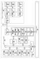
図1は、本明細書で説明される実施形態の1つ又は複数の態様を実装するように構成されたコンピュータ処理システム100を示すブロック図である。コンピュータ処理システム100は、1つ又は複数のプロセッサ102と、メモリハブ105を含み得る相互接続経路を介して通信するシステムメモリ104とを有する処理サブシステム101を含む。メモリハブ105は、チップセットコンポーネント内の別個のコンポーネントであってもよく、1つ又は複数のプロセッサ102に統合されてもよい。メモリハブ105は、通信リンク106を介してI/Oサブシステム111に結合されている。I/Oサブシステム111は、コンピュータ処理システム100が1つ又は複数の入力デバイス108から入力を受信するのを可能にし得るI/Oハブ107を含む。さらに、I/Oハブ107は、1つ又は複数のプロセッサ102に含まれ得るディスプレイコントローラが1つ又は複数の表示デバイス110Aに出力を供給するのを可能にできる。1つの実施形態において、I/Oハブ107に結合された1つ又は複数の表示デバイス110Aは、ローカルの、内蔵型の、又は埋め込み型の表示デバイスを含んでよい。 FIG. 1 is a block diagram showing a
処理サブシステム101は、例えば、バス又は他の通信リンク113を介してメモリハブ105に結合された1つ又は複数の並列プロセッサ112を含む。通信リンク113は、任意の数の規格ベースの通信リンク技術又はプロトコル(限定されることはないが、PCI Expressなど)のうちの1つであってもよく、ベンダ固有の通信インタフェース又は通信ファブリックであってもよい。1つ又は複数の並列プロセッサ112は、計算に重点を置いた、多数の処理コア及び/又は処理クラスタを含むことができる並列又はベクトル処理システム(多数のコアを統合した(many integrated core:MIC)プロセッサなど)を形成してよい。例えば、1つ又は複数の並列プロセッサ112は、I/Oハブ107を介して結合された1つ又は複数の表示デバイス110Aのうちの1つにピクセルを出力できるグラフィックス処理サブシステムを形成する。1つ又は複数の並列プロセッサ112は、1つ又は複数の表示デバイス110Bへの直接的な接続を可能にするディスプレイコントローラ及びディスプレイインタフェース(不図示)も含んでよい。 The processing subsystem 101 includes, for example, one or more
I/Oサブシステム111では、システムストレージユニット114がI/Oハブ107に接続して、コンピュータ処理システム100にストレージメカニズムを提供できる。I/Oスイッチ116が、インタフェースメカニズムを提供するのに用いられ、I/Oハブ107と、このプラットフォームに統合され得るネットワークアダプタ118及び/又は無線ネットワークアダプタ119などの他のコンポーネントと、1つ又は複数のアドインデバイス120を介して追加され得る様々な他のデバイスとの接続を可能にしてよい。アドインデバイス120は、例えば、1つ又は複数の外付けグラフィックスプロセッサデバイス及び/又はコンピュートアクセラレータも含んでよい。ネットワークアダプタ118は、イーサネット(登録商標)アダプタであっても、別の有線ネットワークアダプタであってもよい。無線ネットワークアダプタ119は、Wi-Fi(登録商標)ネットワークデバイス、Bluetooth(登録商標)ネットワークデバイス、近距離無線通信(NFC)ネットワークデバイス、あるいは1つ又は複数の無線機を含む他のネットワークデバイスのうちの1つ又は複数を含んでよい。 In the I / O subsystem 111, the system storage unit 114 can be connected to the I /
コンピュータ処理システム100は、USBポート接続又は他のポート接続、光学ストレージドライブ、及びビデオキャプチャデバイスなどを含む明示的に示されていない他のコンポーネントを含んでよく、I/Oハブ107にも接続されてよい。図1の様々なコンポーネントを相互接続する通信経路が、PCI(Peripheral Component Interconnect)ベースのプロトコル(例えば、PCI-Express)などの任意の好適なプロトコル、あるいはNV-Link高速相互接続などの任意の他のバス又はポイントツーポイント通信インタフェース及び/若しくはプロトコル、又は当技術分野で知られている相互接続プロトコルを用いて実装されてよい。 The
1つ又は複数の並列プロセッサ112は、グラフィックス及び映像の処理に最適化された回路(例えば、ビデオ出力回路を含む)を組み込んでよく、グラフィックス処理ユニット(GPU)を構成する。代替的に又は追加的に、1つ又は複数の並列プロセッサ112は、汎用処理に最適化された回路を組み込んでよく、それと共に、本明細書でより詳細に説明される基礎的な計算アーキテクチャを保持する。コンピュータ処理システム100の各コンポーネントは、単一の集積回路上にある1つ又は複数の他のシステム要素と統合されてよい。例えば、1つ又は複数の並列プロセッサ112、メモリハブ105、プロセッサ102、及びI/Oハブ107は、システムオンチップ(SoC)型集積回路に統合されてよい。あるいは、コンピュータ処理システム100の各コンポーネントは、単一のパッケージに統合されて、システムインパッケージ(SIP)構成を形成してよい。1つの実施形態では、コンピュータ処理システム100のコンポーネントの少なくとも一部がマルチチップモジュール(MCM)に統合されてよく、当該マルチチップモジュールは、他のマルチチップモジュールと相互接続されてモジュール式コンピュータ処理システムになり得る。 The one or more
本明細書に示されるコンピュータ処理システム100は例示であり、変形及び修正があり得ることが理解されるであろう。ブリッジの数及び配置、プロセッサ102の数、並びに並列プロセッサ112の数を含む接続トポロジは、要求通りに修正されてよい。例えば、システムメモリ104は、ブリッジを通じてではなく、プロセッサ102に直接的に接続されてよく、他のデバイスはメモリハブ105及びプロセッサ102を介してシステムメモリ104と通信する。他の代替トポロジにおいて、並列プロセッサ112は、メモリハブ105ではなくI/Oハブ107に、あるいは1つ又は複数のプロセッサ102のうちの1つに直接的に接続される。他の実施形態において、I/Oハブ107及びメモリハブ105は単一のチップに統合されてよい。プロセッサ102の2つ又はそれより多くのセットを複数のソケットを介して取り付けることも可能であり、これらのソケットは、並列プロセッサ112の2つ又はそれより多くのインスタンスと結合できる。 It will be appreciated that the
本明細書に示される特定のコンポーネントの一部は任意的であり、コンピュータ処理システム100の全ての実装形態に含まれなくてもよい。例えば、任意の数のアドインカード又は周辺機器がサポートされてもよく、いくつかのコンポーネントが除外されてもよい。さらに、いくつかのアーキテクチャが、図1に示すものと同様のコンポーネントに異なる用語を用いてもよい。例えば、メモリハブ105は、いくつかのアーキテクチャではノースブリッジと呼ばれることがあり、I/Oハブ107はサウスブリッジと呼ばれることがある。 Some of the particular components shown herein are optional and may not be included in all implementations of
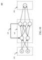
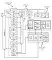
図2Aは、並列プロセッサ200を示している。並列プロセッサ200は、本明細書で説明されるGPU又はGPGPUなどであってよい。並列プロセッサ200の様々なコンポーネントは、プログラム可能型プロセッサ、特定用途向け集積回路(ASIC)、又はフィールドプログラマブルゲートアレイ(FPGA)などの1つ又は複数の集積回路デバイスを用いて実装されてよい。図示されている並列プロセッサ200は、図1に示す並列プロセッサ112であっても、そのうちの1つであってもよい。 FIG. 2A shows a
並列プロセッサ200は並列処理ユニット202を含む。並列処理ユニットは、並列処理ユニット202の他のインスタンスを含む他のデバイスとの通信を可能にするI/Oユニット204を含む。I/Oユニット204は、他のデバイスに直接的に接続されてよい。例えば、I/Oユニット204は、メモリハブ105などのハブ又はスイッチインタフェースの使用を介して他のデバイスと接続する。メモリハブ105とI/Oユニット204との接続によって、通信リンク113が形成される。並列処理ユニット202において、I/Oユニット204はホストインタフェース206及びメモリクロスバー216と接続する。ホストインタフェース206は処理操作の実行を対象とするコマンドを受信し、メモリクロスバー216はメモリ操作の実行を対象とするコマンドを受信する。 The
ホストインタフェース206がI/Oユニット204を介してコマンドバッファを受信すると、ホストインタフェース206は、これらのコマンドを実行するための作業操作をフロントエンド208に送ることができる。1つの実施形態において、フロントエンド208は、コマンド又は他の作業項目を処理クラスタアレイ212に配分するように構成されているスケジューラ210と結合する。スケジューラ210は、処理クラスタアレイ212の処理クラスタにタスクが配分される前に必ず、処理クラスタアレイ212が適切に構成され且つ有効状態になるようにする。スケジューラ210は、マイクロコントローラ上で実行するファームウェアロジックによって実装されてよい。マイクロコントローラで実装されるスケジューラ210は、複雑なスケジューリングと作業配分操作とを粗粒度及び細粒度で行い、処理アレイ212上で実行しているスレッドの速やかなプリエンプション及びコンテキスト切り替えを可能にするように構成可能である。ホストソフトウェアは、複数のグラフィックス処理ドアベルのうちの1つを介して、処理アレイ212に対してスケジューリングするワークロードを確かめられることが好ましい。ワークロードは次に、スケジューラマイクロコントローラ内のスケジューラ210のロジックにより、処理アレイ212全体に自動的に配分されてよい。 When the host interface 206 receives a command buffer via the I /
処理クラスタアレイ212は、「N個」までの処理クラスタ(例えば、クラスタ214A、クラスタ214B、…、クラスタ214N)を含んでよい。処理クラスタアレイ212の各クラスタ214A~214Nは、多数の同時スレッドを実行できる。スケジューラ210は、プログラム又は計算のタイプごとに発生するワークロードに応じて変わり得る様々なスケジューリングアルゴリズム及び/又は作業配分アルゴリズムを用いて、処理クラスタアレイ212のクラスタ214A~214Nに作業を割り当てることができる。スケジューリングは、スケジューラ210によって動的に処理されてもよく、処理クラスタアレイ212による実行のために構成されたプログラムロジックのコンパイル時に、コンパイラロジックによって部分的に支援されてもよい。必要に応じて、処理クラスタアレイ212の個々のクラスタ214A~214Nが、異なるタイプのプログラムを処理するために、又は異なるタイプの計算を行うために割り当てられてよい。 The processing cluster array 212 may include up to "N" processing clusters (eg,
処理クラスタアレイ212は、様々なタイプの並列処理操作を行うように構成されてよい。例えば、クラスタアレイ212は、汎用並列コンピュート操作を行うように構成されている。例えば、処理クラスタアレイ212は、ビデオデータ及び/又はオーディオデータのフィルタリング、物理演算を含むモデリング操作の実行、及びデータ変換の実行を含む処理タスクを実行するロジックを含んでよい。 The processing cluster array 212 may be configured to perform various types of parallel processing operations. For example, the cluster array 212 is configured to perform general purpose parallel compute operations. For example, the processing cluster array 212 may include logic to perform processing tasks including filtering video and / or audio data, performing modeling operations including physics, and performing data conversions.
処理クラスタアレイ212は、並列グラフィックス処理操作を行うように構成されている。並列プロセッサ200がグラフィックス処理操作を行うように構成されているそのような実施形態において、処理クラスタアレイ212は、そのようなグラフィックス処理操作の実行をサポートする別のロジックを含んでよく、そのようなロジックには、限定されることはないが、テクスチャ操作を行うテクスチャサンプリングロジック、並びにテセレーションロジック及び他の頂点処理ロジックが含まれる。さらに、処理クラスタアレイ212は、グラフィックス処理関連のシェーダプログラムを実行するように構成されてよく、そのようなシェーダプログラムには、限定されることはないが、頂点シェーダ、テセレーションシェーダ、ジオメトリシェーダ、及びピクセルシェーダなどがある。並列処理ユニット202は、I/Oユニット204を介して処理のために、システムメモリからデータを転送できる。処理する際、転送されたデータは処理中にオンチップメモリ(例えば、並列プロセッサメモリ222)に格納され、次いでシステムメモリにライトバックされてよい。 The processing cluster array 212 is configured to perform parallel graphics processing operations. In such an embodiment in which the
並列処理ユニット202を用いてグラフィックス処理を行う実施形態において、スケジューラ210は、処理ワークロードをほぼ等しいサイズの複数のタスクに分割して、処理クラスタアレイ212の複数のクラスタ214A~214Nにグラフィックス処理操作をより効果的に配分できるように構成されてよい。これらの実施形態のいくつかでは、処理クラスタアレイ212の一部が、異なるタイプの処理を行うように構成されてよい。例えば、レンダリングされた表示用の画像を生成するために、第1部分が頂点シェーディング及びトポロジ生成を行うように構成されてよく、第2部分がテセレーション及びジオメトリシェーディングを行うように構成されてよく、第3部分がピクセルシェーディング又は他のスクリーン空間操作を行うように構成されてよい。クラスタ214A~214Nのうちの1つ又は複数によって生成される中間データがバッファに格納され、当該中間データがさらなる処理のためにクラスタ214A~214Nに送られることを可能にしてよい。 In an embodiment in which graphics processing is performed using the parallel processing unit 202, the scheduler 210 divides the processing workload into a plurality of tasks having substantially the same size, and graphics in a plurality of
動作に際して、処理クラスタアレイ212は、実行される処理タスクをスケジューラ210を介して受信でき、スケジューラ210は、処理タスクを定めるコマンドをフロントエンド208から受信する。グラフィックス処理操作では、処理タスクが、処理されるデータ(例えば、サーフェス(パッチ)データ、プリミティブデータ、頂点データ、及び/又はピクセルデータ)のインデックス、並びにデータがどのように処理されるのか(例えば、どのプログラムが実行されるのか)を定める状態パラメータ及びコマンドを含んでよい。スケジューラ210は、当該タスクに対応するインデックスをフェッチするように構成されてもよく、このインデックスをフロントエンド208から受信してもよい。フロントエンド208は、受信コマンドバッファ(例えば、バッチバッファ、プッシュバッファなど)により指定されるワークロードが開始される前に必ず、処理クラスタアレイ212が有効状態になるように構成されるように構成されてよい。 During operation, the processing cluster array 212 can receive the processing task to be executed via the scheduler 210, and the scheduler 210 receives a command defining the processing task from the
並列処理ユニット202の1つ又は複数のインスタンスのそれぞれは、並列プロセッサメモリ222と結合できる。並列プロセッサメモリ222は、メモリクロスバー216を介してアクセスされてよく、当該メモリクロスバーは処理クラスタアレイ212及びI/Oユニット204からメモリ要求を受信できる。メモリクロスバー216は、並列プロセッサメモリ222にメモリインタフェース218を介してアクセスできる。メモリインタフェース218は、それぞれが並列プロセッサメモリ222の一部(例えば、メモリユニット)に結合できる複数のパーティションユニット(例えば、パーティションユニット220A、パーティションユニット220B、…、パーティションユニット220N)を含んでよい。第1パーティションユニット220Aが、対応する第1メモリユニット224Aを有し、第2パーティションユニット220Bが、対応するメモリユニット224Bを有し、第Nパーティションユニット220Nが、対応する第Nメモリユニット224Nを有するように、パーティションユニット220A~220Nの数はメモリユニットの数と等しくなるように構成されてよい。他の実施形態において、パーティションユニット220A~220Nの数は、メモリデバイスの数と等しくなくてもよい。 Each of one or more instances of the parallel processing unit 202 can be combined with the parallel processor memory 222. The parallel processor memory 222 may be accessed via the memory crossbar 216, which can receive memory requests from the processing cluster array 212 and the I /
メモリユニット224A~224Nは、ダイナミックランダムアクセスメモリ(DRAM)、又はグラフィックスダブルデータレート(GDDR)メモリを含む同期式グラフィックスランダムアクセスメモリ(SGRAM)などのグラフィックスランダムアクセスメモリを含む様々なタイプのメモリデバイスを含んでよい。必要に応じて、メモリユニット224A~224Nは、限定されることはないが、高帯域幅メモリ(HBM)を含む3Dスタックメモリも含んでよい。当業者であれば、メモリユニット224A~224Nの具体的な実装形態は様々であってよく、様々な従来方式のうちの1つから選択されてよいことを理解するであろう。フレームバッファ又はテクスチャマップなどのレンダーターゲットがメモリユニット224A~224Nの全体に格納され、パーティションユニット220A~220Nが、各レンダーターゲットの一部を並列に書き込み、並列プロセッサメモリ222の利用可能な帯域幅を効率的に用いることを可能にしてよい。いくつかの実施形態では、並列プロセッサメモリ222のローカルインスタンスが、ローカルキャッシュメモリと併用してシステムメモリを利用する統合メモリ方式を優先して除外されてよい。 Memory units 224A-224N are of various types including dynamic random access memory (DRAM) or graphics random access memory such as synchronous graphics random access memory (SGRAM) including graphics double data rate (GDDR) memory. It may include a memory device. If desired, the memory units 224A-224N may also include, but are not limited to, 3D stack memory including high bandwidth memory (HBM). Those skilled in the art will appreciate that the specific implementation of the memory units 224A-224N may vary and may be selected from one of a variety of conventional methods. Render targets such as frame buffers or texture maps are stored in the entire memory units 224A-224N, and
必要に応じて、処理クラスタアレイ212のクラスタ214A~214Nのうちのいずれか1つが、並列プロセッサメモリ222内のメモリユニット224A~224Nのうちのいずれかに書き込まれるデータを処理する能力を有する。メモリクロスバー216は、各クラスタ214A~214Nの出力を任意のパーティションユニット220A~220N又は別のクラスタ214A~214Nに転送するように構成されてよく、このパーティションユニット又は別のクラスタは、出力に対して別の処理操作を行うことができる。各クラスタ214A~214Nは、メモリクロスバー216を通じてメモリインタフェース218と通信して、様々な外付けメモリデバイスとの間で読み出し又は書き込みを行うことができる。メモリクロスバー216を有する実施形態のうちの1つにおいて、メモリクロスバー216は、I/Oユニット204と通信するためのメモリインタフェース218への接続と、並列プロセッサメモリ222のローカルインスタンスへの接続とを有し、異なる処理クラスタ214A~214N内の処理ユニットが並列処理ユニット202のローカルではないシステムメモリ又は他のメモリと通信することを可能にする。一般に、メモリクロスバー216は、例えば、クラスタ214A~214Nとパーティションユニット220A~220Nとの間のトラフィックストリームを分離するのに仮想チャネルを用いることができてよい。 If necessary, any one of
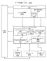
並列プロセッサ200には並列処理ユニット202の1つのインスタンスが示されているが、並列処理ユニット202の任意の数のインスタンスが含まれてよい。例えば、並列処理ユニット202の複数のインスタンスを1つのアドインカードに設けることができ、複数のアドインカードを相互接続することができる。並列処理ユニット202の個々のインスタンスは、個々のインスタンスが異なる数の処理コア、異なる量のローカル並列プロセッサメモリ、及び/又は他の構成上の違いを有していても、相互に連動するように構成されてよい。必要に応じて、並列処理ユニット202の一部のインスタンスが他のインスタンスよりも高精度の浮動小数点ユニット264を含んでよい。並列処理ユニット202又は並列プロセッサ200の1つ又は複数のインスタンスを組み込むシステムが、様々な構成及びフォームファクタで実現されてよく、このシステムには、限定されることはないが、デスクトップ、ラップトップ、ハンドヘルド型パーソナルコンピュータ、サーバ、ワークステーション、ゲームコンソール、及び/又は埋め込みシステムが含まれる。 Although one instance of the parallel processing unit 202 is shown in the
図2Bは、パーティションユニット220のブロック図である。パーティションユニット220は、図2Aに示すパーティションユニット220A~220Nのうちの1つのインスタンスであってよい。図示されているように、パーティションユニット220は、L2キャッシュ221、メタデータ(例えば、コントロールサーフェスアップデート、圧縮値)を格納するメタデータキャッシュ224、フレームバッファインタフェース225、及びROP226(ラスタ操作ユニット)を含む。L2キャッシュ221は、メモリクロスバー216及びROP226から受信するロード操作及びストア操作を行うように構成された読み出し/書き込みキャッシュである。読み出しミス及び緊急のライトバック要求が、処理のためにL2キャッシュ221によってフレームバッファインタフェース225に出力される。これらのアップデートも、処理のためにフレームバッファインタフェース225を介してフレームバッファに送信されてよい。1つの実施形態において、フレームバッファインタフェース225は、図2Aに示すメモリユニット224A~224Nなどの、並列プロセッサメモリ内の(例えば、並列プロセッサメモリ222内の)複数のメモリユニットのうちの1つとインタフェースで接続する。パーティションユニット220も、追加的に又は代替的に、並列プロセッサメモリ内の複数のメモリユニットのうちの1つとメモリコントローラ(不図示)を介してインタフェースで接続してよい。 FIG. 2B is a block diagram of the
グラフィックスアプリケーションでは、ROP226は、ステンシル、zテスト、及びブレンディングなどのラスタ操作を行う処理ユニットである。ROP226は次いで、グラフィックスメモリに格納されている処理済みのグラフィックスデータを出力する。いくつかの実施形態において、ROP226は、メモリに書き込まれるデプスデータ及びカラーデータを圧縮し且つメモリから読み出されたデプスデータ又はカラーデータを復元する圧縮ロジックを含む。圧縮ロジックは、複数の圧縮アルゴリズムのうちの1つ又は複数を利用する可逆圧縮ロジックであってよい。ROP226により行われる圧縮のタイプは、圧縮されるデータの統計的特性に基づいて異なってよい。例えば、1つの実施形態では、デプスデータ及びカラーデータに対してデルタカラー圧縮がタイルごとに行われる。 In graphics applications, the ROP226 is a processing unit that performs raster operations such as stencil, ztest, and blending. The
ROP226は、パーティションユニット220に含まれる代わりに、各処理クラスタ(例えば、図2Aのクラスタ214A~214N)に含まれてもよい。そのような実施形態では、ピクセルデータの読み出し要求及び書き込み要求が、ピクセルフラグメントデータの代わりに、メモリクロスバー216によって送られる。処理済みのグラフィックスデータは、図1に示す1つ又は複数の表示デバイス110のうちの1つなどの表示デバイスに表示され、プロセッサ102によるさらなる処理のために送られても、図2Aに示す並列プロセッサ200内の複数の処理エンティティのうちの1つによるさらなる処理のために送られてもよい。 ROP226 may be included in each processing cluster (for example,
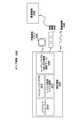
図2Cは、並列処理ユニット内の処理クラスタ214のブロック図である。例えば、処理クラスタは、図2Aに示す処理クラスタ214A~214Nのうちの1つのインスタンスである。処理クラスタ214は、多くのスレッドを並列に実行するように構成されてよく、「スレッド」という用語は、特定のセットの入力データに対して実行される特定のプログラムのインスタンスを意味する。必要に応じて、複数の独立した命令ユニットを提供するのではなく、単一命令複数データ(SIMD)型の命令発行技法が、多数のスレッドの並列実行をサポートするのに用いられてよい。あるいは、複数の処理クラスタのそれぞれにある処理エンジンのセットに命令を発行するように構成された共通の命令ユニットを用いて、単一命令複数スレッド(SIMT)技法が、通常、同期した多数のスレッドの並列実行をサポートするのに用いられてよい。全ての処理エンジンが通常全く同じ命令を実行するSIMD実行方式とは異なり、SIMT実行では、個々のスレッドが所与のスレッドプログラムによって分岐実行パスをより容易にたどることが可能になる。当業者であれば、SIMD処理方式が、SIMT処理方式の機能的サブセットを表していることを理解するであろう。 FIG. 2C is a block diagram of the
処理クラスタ214の操作が、処理タスクをSIMT並列プロセッサに配分するパイプラインマネージャ232を介して制御されてよい。パイプラインマネージャ232は、図2Aのスケジューラ210から命令を受信し、これらの命令の実行をグラフィックスマルチプロセッサ234及び/又はテクスチャユニット236を介して管理する。図示されたグラフィックスマルチプロセッサ234は、SIMT並列プロセッサの例示的なインスタンスである。しかしながら、異なるアーキテクチャの様々なタイプのSIMT並列プロセッサが、処理クラスタ214に含まれてもよい。グラフィックスマルチプロセッサ234の1つ又は複数のインスタンスが、処理クラスタ214に含まれてもよい。グラフィックスマルチプロセッサ234はデータを処理することができ、データクロスバー240が、処理済みのデータを、他のシェーダユニットを含む複数の考え得る送信先のうちの1つに配分するのに用いられてよい。パイプラインマネージャ232は、データクロスバー240を介して配分される処理済みのデータの送信先を指定することで、処理済みのデータの配分を容易にすることができる。 The operation of the
処理クラスタ214内の各グラフィックスマルチプロセッサ234は、全く同じセットの機能実行ロジック(例えば、算術論理ユニット、ロードストアユニットなど)を含んでよい。機能実行ロジックは、前の命令が完了する前に新たな命令を発行できるパイプライン方式で構成されてよい。機能実行ロジックは、整数及び浮動小数点算術、比較演算、ブール演算、ビットシフト、及び様々な代数関数の計算を含む様々な演算をサポートする。同じ機能ユニットのハードウェアを活用すれば、様々な演算を行うことができ、また、機能ユニットのあらゆる組み合わせが存在し得る。 Each graphics multiprocessor 234 in the
処理クラスタ214に送られる命令は、スレッドを構成する。並列処理エンジンのセット全体で実行するスレッドのセットが、スレッドグループである。スレッドグループは、異なる入力データに対して同じプログラムを実行する。スレッドグループ内の各スレッドは、グラフィックスマルチプロセッサ234内の異なる処理エンジンに割り当てられてよい。スレッドグループは、グラフィックスマルチプロセッサ234内の処理エンジンの数よりも少ないスレッドを含んでよい。スレッドグループが処理エンジンの数よりも少ないスレッドを含んでいる場合、これらの処理エンジンのうちの1つ又は複数が、スレッドグループの処理サイクル中に休止していてもよい。スレッドグループは、グラフィックスマルチプロセッサ234内の処理エンジンの数より多くのスレッドも含んでよい。スレッドグループがグラフィックスマルチプロセッサ234内の処理エンジンの数より多くのスレッドを含む場合、連続したクロックサイクルにわたって処理を実行できる。必要に応じて、グラフィックスマルチプロセッサ234で複数のスレッドグループが同時に実行されてもよい。 Instructions sent to
グラフィックスマルチプロセッサ234は、ロード操作及びストア操作を行うための内蔵キャッシュメモリを含んでよい。必要に応じて、グラフィックスマルチプロセッサ234は内蔵キャッシュなしで済ませ、処理クラスタ214内のキャッシュメモリ(例えば、L1キャッシュ248)を用いることができる。各グラフィックスマルチプロセッサ234は、全ての処理クラスタ214に共有され且つスレッド間でデータを転送するのに用いられ得る、パーティションユニット(例えば、図2Aのパーティションユニット220A~220N)内のL2キャッシュにもアクセスできる。グラフィックスマルチプロセッサ234は、オフチップグローバルメモリにもアクセスしてよく、このメモリはローカル並列プロセッサメモリ及び/又はシステムメモリのうちの一方又は両方を含んでよい。並列処理ユニット202の外部にある任意のメモリが、グローバルメモリとして用いられてよい。処理クラスタ214がグラフィックスマルチプロセッサ234の複数のインスタンスを含む実施形態では、L1キャッシュ248に格納され得る共通の命令及びデータを共有できる。 The
各処理クラスタ214は、仮想アドレスを物理アドレスにマッピングするように構成されたMMU(メモリ管理ユニット)245を含んでよい。他の実施形態では、MMU245の1つ又は複数のインスタンスが、図2Aのメモリインタフェース218に存在してよい。MMU245は、仮想アドレスをタイルの物理アドレス及び必要に応じてキャッシュラインインデックスにマッピングするのに用いられるページテーブルエントリ(PTE)のセットを含む。MMU245は、グラフィックスマルチプロセッサ234又はL1キャッシュ又は処理クラスタ214に存在し得るアドレス変換ルックアサイドバッファ(TLB)若しくはキャッシュを含んでよい。物理アドレスが処理されて、サーフェスデータアクセスの局所性が配分され、パーティションユニット間で効率的なリクエストインタリーブを可能にする。キャッシュラインインデックスは、キャッシュラインの要求がヒットなのかミスなのかを判定するのに用いられてよい。 Each
グラフィックスアプリケーション及びコンピュータ処理アプリケーションにおいて、処理クラスタ214は、テクスチャマッピング操作を行うための、例えば、テクスチャサンプル位置の決定、テクスチャデータの読み出し、及びテクスチャデータのフィルタリングを行うためのテクスチャユニット236に各グラフィックスマルチプロセッサ234が結合されるように構成され得る。テクスチャデータは、内蔵テクスチャL1キャッシュ(不図示)から、又はいくつかの実施形態ではグラフィックスマルチプロセッサ234内のL1キャッシュから読み出され、必要に応じて、L2キャッシュ、ローカル並列プロセッサメモリ、又はシステムメモリからフェッチされる。各グラフィックスマルチプロセッサ234は、処理済みのタスクをデータクロスバー240に出力し、さらなる処理のために処理済みのタスクを別の処理クラスタ214に提供するか、又は処理済みのタスクをメモリクロスバー216を介してL2キャッシュ、ローカル並列プロセッサメモリ、又はシステムメモリに格納する。プリROP242(プリラスタ操作ユニット)が、グラフィックスマルチプロセッサ234からデータを受信し、データをROPユニットに送るように構成されており、ROPユニットは、本明細書で説明したパーティションユニット(例えば、図2Aのパーティションユニット220A~220N)と共に配置されてよい。プリROP242ユニットは、カラーブレンディングの最適化を行い、ピクセルカラーデータを編成し、アドレス変換を行うことができる。 In a graphics application and a computer processing application, the
本明細書で説明されるコアアーキテクチャは例示であり、変形及び修正があり得ることが理解されるであろう。任意の数の処理ユニット、例えば、グラフィックスマルチプロセッサ234、テクスチャユニット236、プリROP242などが、処理クラスタ214に含まれてよい。さらに、1つの処理クラスタ214しか示されていないが、本明細書で説明される並列処理ユニットは、処理クラスタ214の任意の数のインスタンスを含んでよい。必要に応じて、各処理クラスタ214は、別個の異なる処理ユニット、L1キャッシュなどを用いて、他の処理クラスタ214から独立して動作するように構成されてよい。 It will be appreciated that the core architecture described herein is exemplary and may be modified and modified. Any number of processing units, such as
図2Dは、グラフィックスマルチプロセッサ234の一例を示しており、ここでは、グラフィックスマルチプロセッサ234は処理クラスタ214のパイプラインマネージャ232と結合する。グラフィックスマルチプロセッサ234は、限定されることはないが、命令キャッシュ252、命令ユニット254、アドレスマッピングユニット256、レジスタファイル258、1つ又は複数の汎用グラフィックス処理ユニット(GPGPU)コア262、及び1つ又は複数のロード/ストアユニット266を含む実行パイプラインを有する。GPGPUコア262及びロード/ストアユニット266は、メモリ及びキャッシュ相互接続268を介して、キャッシュメモリ272及び共有メモリ270に結合されている。グラフィックスマルチプロセッサ234はさらに、行列演算及び/又はレイトレーシング操作を加速させるハードウェアロジックを含むテンソル及び/又はレイトレーシングコア263を含んでよい。 FIG. 2D shows an example of the
命令キャッシュ252は、パイプラインマネージャ232から、実行する一連の命令を受信してよい。これらの命令は命令キャッシュ252にキャッシュされ、命令ユニット254による実行のためにディスパッチされる。命令ユニット254は、スレッドグループ(例えば、ワープ)として命令をディスパッチでき、スレッドグループの各スレッドがGPGPUコア262内の様々な実行ユニットに割り当てられる。命令は、統合アドレス空間内のアドレスを指定することで、ローカルアドレス空間、共有アドレス空間、又はグローバルアドレス空間のうちのいずれかにアクセスできる。アドレスマッピングユニット256は、統合アドレス空間内のアドレスを、ロード/ストアユニット266がアクセスできる別のメモリアドレスに変換するのに用いられてよい。 The
レジスタファイル258は、グラフィックスマルチプロセッサ234の機能ユニットにレジスタのセットを提供する。レジスタファイル258は、グラフィックスマルチプロセッサ234の機能ユニット(例えば、GPGPUコア262、ロード/ストアユニット266)のデータパスに接続されたオペランド用一時記憶を提供する。レジスタファイル258は、各機能ユニットがレジスタファイル258の専用部分に割り当てられるように、各機能ユニットに分割されてよい。例えば、レジスタファイル258は、グラフィックスマルチプロセッサ234が実行する様々なワープに分割されてよい。 The
これらのGPGPUコア262はそれぞれ、グラフィックスマルチプロセッサ234の命令を実行するのに用いられる機能ユニット(例えば、浮動小数点ユニット264(FPU)及び/又は整数算術論理ユニット(ALU))を含んでよい。いくつかの実装形態において、GPGPUコア262は、別の場合にはテンソル及び/又はレイトレーシングコア263内に存在し得るハードウェアロジックを含んでよい。これらのGPGPUコア262はアーキテクチャが同様であってもよく、アーキテクチャが異なっていてもよい。例えば、1つの実施形態では、GPGPUコア262の第1部分が単精度FPU及び整数ALUを含み、GPGPUコアの第2部分が倍精度FPUを含む。必要に応じて、FPUは、浮動小数点算術用のIEEE754-2008規格を実装できる、又は可変精度の浮動小数点算術を可能にできる。グラフィックスマルチプロセッサ234はさらに、長方形コピー操作又はピクセルブレンディング操作などの特定の機能を行う1つ又は複数の固定機能ユニット又は特殊機能ユニットを含んでよい。複数のGPGPUコアのうちの1つ又は複数も、固定機能ロジック又は特殊機能ロジックを含んでよい。 Each of these GPGPU cores 262 may include functional units used to execute instructions on the graphics multiprocessor 234 (eg, floating point unit 264 (FPU) and / or integer arithmetic logic unit (ALU)). In some implementations, the GPGPU core 262 may otherwise include hardware logic that may be present within the tensor and / or
GPGPUコア262は、データの複数のセットに対して単一命令を実行できるSIMDロジックを含んでよい。必要に応じて、GPGPUコア262は、SIMD4命令、SIMD8命令、及びSIMD16命令を物理的に実行でき、SIMD1命令、SIMD2命令、及びSIMD32命令を論理的に実行できる。GPGPUコア用のSIMD命令は、コンパイル時にシェーダコンパイラによって生成されてもよく、単一プログラム複数データ(SPMD)アーキテクチャ又はSIMTアーキテクチャ用に記述されコンパイルされたプログラムを実行するときに自動的に生成されてもよい。SIMT実行モデル用に構成されたプログラムの複数のスレッドが、1つのSIMD命令によって実行されてよい。例えば、1つの実施形態では、同じ又は同様の操作を行う8個のSIMTスレッドが、1つのSIMD8論理ユニットによって並列に実行されてよい。 The GPGPU core 262 may include SIMD logic capable of executing a single instruction on multiple sets of data. If necessary, the GPGPU core 262 can physically execute the SIMD4 instruction, the SIMD8 instruction, and the SIMD16 instruction, and can logically execute the SIMD1 instruction, the SIMD2 instruction, and the SIMD32 instruction. SIMD instructions for GPGPU cores may be generated by the shader compiler at compile time and are automatically generated when running a program written and compiled for a single program multiple data (SPMD) architecture or SIMT architecture. May be good. Multiple threads of the program configured for the SIMT execution model may be executed by one SIMD instruction. For example, in one embodiment, eight SIMT threads performing the same or similar operations may be executed in parallel by one SIMD8 logical unit.
メモリ及びキャッシュ相互接続268は、グラフィックスマルチプロセッサ234の各機能ユニットをレジスタファイル258及び共有メモリ270に接続する相互接続ネットワークである。例えば、メモリ及びキャッシュ相互接続268は、ロード/ストアユニット266が共有メモリ270とレジスタファイル258との間でロード操作及びストア操作を行うのを可能にするクロスバー相互接続である。レジスタファイル258はGPGPUコア262と同じ周波数で動作できるので、GPGPUコア262とレジスタファイル258との間のデータ転送遅延が非常に低い。共有メモリ270は、グラフィックスマルチプロセッサ234内の機能ユニットで実行するスレッド間の通信を可能にするのに用いられてよい。キャッシュメモリ272は、例えば、機能ユニットとテクスチャユニット236との間で通信されるテクスチャデータをキャッシュするデータキャッシュとして用いられてよい。共有メモリ270も、プログラム管理キャッシュとして用いられてよい。GPGPUコア262で実行するスレッドは、キャッシュメモリ272に格納される自動的にキャッシュされるデータに加えて、データを共有メモリにプログラムで格納できる。 The memory and
図3A~図3Cは、複数の実施形態による別のグラフィックスマルチプロセッサを示している。図3A~図3Bはグラフィックスマルチプロセッサ325、350を示している。これらは、図2Cのグラフィックスマルチプロセッサ234に関連しており、そのうちの1つの代わりに用いられてよい。したがって、グラフィックスマルチプロセッサ234と組み合わせたあらゆる機能のここでの開示は、グラフィックスマルチプロセッサ325、350との対応する組み合わせも開示するが、そのように限定されることはない。図3Cは、グラフィックスマルチプロセッサ325、350に対応するマルチコアグループ365A~365Nに配置される専用のグラフィックス処理リソースのセットを含むグラフィックス処理ユニット(GPU)380を示している。図示されたグラフィックスマルチプロセッサ325、350、及びマルチコアグループ365A~365Nは、多数の実行スレッドの同時実行ができるストリーミングマルチプロセッサ(SM)であってよい。 3A-3C show different graphics multiprocessors according to a plurality of embodiments. 3A-3B show graphics multiprocessors 325, 350. These are related to the
図3Aのグラフィックスマルチプロセッサ325は、図2Dのグラフィックスマルチプロセッサ234と比べて、実行リソースユニットの複数の別のインスタンスを含む。例えば、グラフィックスマルチプロセッサ325は、命令ユニット332A~332B、レジスタファイル334A~334B、及びテクスチャユニット344A~344Bという複数のインスタンスを含んでよい。グラフィックスマルチプロセッサ325は、グラフィックス実行ユニット又はコンピュート実行ユニット(例えば、GPGPUコア336A~336B、テンソルコア337A~337B、レイトレーシングコア338A~338B)の複数のセット、及びロード/ストアユニット340A~340Bの複数のセットも含む。実行リソースユニットは、共通の命令キャッシュ330、テクスチャ及び/又はデータキャッシュメモリ342、並びに共有メモリ346を有する。 The graphics multiprocessor 325 of FIG. 3A contains a plurality of separate instances of the execution resource unit as compared to the
様々なコンポーネントは、相互接続ファブリック327を介して通信することができる。相互接続ファブリック327は、グラフィックスマルチプロセッサ325の様々なコンポーネント間の通信を可能にする1つ又は複数のクロスバースイッチを含んでよい。相互接続ファブリック327は、別個の高速ネットワークファブリック層であってもよく、この層の上に、グラフィックスマルチプロセッサ325の各コンポーネントがスタックされる。グラフィックスマルチプロセッサ325の各コンポーネントは、相互接続ファブリック327を介して遠隔コンポーネントと通信する。例えば、GPGPUコア336A~336B、337A~337B、及び338A~338Bはそれぞれ、相互接続ファブリック327を介して共有メモリ346と通信できる。相互接続ファブリック327は、グラフィックスマルチプロセッサ325内の通信を調停して、コンポーネント間の公平な帯域幅割り当てを確保できる。 The various components can communicate via the interconnect fabric 327. The interconnect fabric 327 may include one or more crossbar switches that allow communication between various components of the graphics multiprocessor 325. The interconnect fabric 327 may be a separate high-speed network fabric layer on which each component of the graphics multiprocessor 325 is stacked. Each component of the graphics multiprocessor 325 communicates with a remote component via the interconnect fabric 327. For example, the GPGPU cores 336A-336B, 337A-337B, and 338A-338B can each communicate with the shared memory 346 via the interconnect fabric 327. The interconnect fabric 327 can arbitrate communication within the graphics multiprocessor 325 to ensure a fair bandwidth allocation between components.
図3Bのグラフィックスマルチプロセッサ350は、実行リソース356A~356Dの複数のセットを含み、実行リソースの各セットは、図2D及び図3Aに示されているように、複数の命令ユニット、レジスタファイル、GPGPUコア、及びロードストアユニットを含む。実行リソース356A~356Dは、命令キャッシュ354及び共有メモリ353を共有しながら、テクスチャ操作用のテクスチャユニット360A~360Dと連携して動作することができる。例えば、実行リソース356A~356Dは、命令キャッシュ354及び共有メモリ353、並びにテクスチャ及び/又はデータキャッシュメモリ358A~358Bの複数のインスタンスを共有できる。様々なコンポーネントは、図3Aの相互接続ファブリック327と同様の相互接続ファブリック352を介して通信できる。 The graphics multiprocessor 350 of FIG. 3B comprises a plurality of sets of execution resources 356A-356D, each set of execution resources having a plurality of instruction units, register files, as shown in FIGS. 2D and 3A. Includes GPGPU core and load store unit. The execution resources 356A to 356D can operate in cooperation with the texture units 360A to 360D for texture operations while sharing the instruction cache 354 and the shared memory 353. For example, the execution resources 356A-356D can share a plurality of instances of the instruction cache 354 and the shared memory 353, as well as the texture and / or the data cache memory 358A-358B. The various components can communicate via an interconnect fabric 352 similar to the interconnect fabric 327 of FIG. 3A.
当業者であれば、図1、図2A~図2D、及び図3A~図3Bで説明したアーキテクチャは、本実施形態の範囲に関して記述的であり、限定しているわけではないことを理解するであろう。したがって、本明細書で説明される技法は、適切に構成されたあらゆる処理ユニットに実装されてよい。そのような処理ユニットは、限定されることはないが、1つ又は複数のモバイルアプリケーションプロセッサ、マルチコア中央演算処理装置(CPU)を含む1つ又は複数のデスクトップ用若しくはサーバ用CPU、図2Aの並列処理ユニット202などの1つ又は複数の並列処理ユニット、及び1つ又は複数のグラフィックスプロセッサ若しくは専用処理ユニットを、本明細書で説明される実施形態の範囲から逸脱することなく含む。 Those skilled in the art will appreciate that the architectures described in FIGS. 1, 2A-2D, and 3A-3B are descriptive and not limiting with respect to the scope of this embodiment. There will be. Therefore, the techniques described herein may be implemented in any well-configured processing unit. Such processing units are, but are not limited to, one or more mobile application processors, one or more desktop or server CPUs including a multi-core central processing unit (CPU), parallel to FIG. 2A. One or more parallel processing units such as the processing unit 202, and one or more graphics processors or dedicated processing units are included without departing from the scope of the embodiments described herein.
本明細書で説明される並列プロセッサ又はGPGPUは、グラフィックス操作、機械学習操作、パターン分析操作、及び汎用GPU(GPGPU)の様々な機能を加速するホスト/プロセッサコアに通信可能に結合されてよい。GPUは、バス又は他の相互接続(例えば、PCIe又はNVLinkなどの高速相互接続)によってホストプロセッサ/コアに通信可能に結合されてよい。他の実施形態において、GPUはコアと同じパッケージ又はチップに統合されて、内蔵プロセッサバス/相互接続によって(つまり、パッケージ又はチップの内部で)コアに通信可能に結合されてよい。GPUが接続される方式に関係なく、プロセッサコアは、作業記述子に含まれるコマンド/命令のシーケンスの形で、GPUに作業を割り当ててよい。GPUは次いで、これらのコマンド/命令を効率的に処理するのに専用回路/ロジックを用いる。 The parallel processor or GP PPU described herein may be communicably coupled to a host / processor core that accelerates various functions of graphics operations, machine learning operations, pattern analysis operations, and general purpose GPUs (GPPPUs). .. The GPU may be communicably coupled to the host processor / core by bus or other interconnect (eg, high speed interconnect such as PCIe or NVLink). In other embodiments, the GPU may be integrated into the same package or chip as the core and communicably coupled to the core by the built-in processor bus / interconnect (ie, inside the package or chip). Regardless of how the GPU is connected, the processor core may assign work to the GPU in the form of a sequence of commands / instructions contained in the work descriptor. The GPU then uses dedicated circuits / logic to efficiently process these commands / instructions.
図3Cは、マルチコアグループ365A~365Nに配置された専用のグラフィックス処理リソースのセットを含むグラフィックス処理ユニット(GPU)380を示している。1つのマルチコアグループ365Aだけの詳細が提供されているが、その他のマルチコアグループ365B~365Nも同じ又は同様のグラフィックス処理リソースのセットを備えてよいことが理解されるであろう。マルチコアグループ365A~365Nに関して説明される詳細が、本明細書で説明されるあらゆるグラフィックスマルチプロセッサ234、325、350にも適用されてよい。 FIG. 3C shows a graphics processing unit (GPU) 380 containing a set of dedicated graphics processing resources arranged in multi-core groups 365A-365N. Although details are provided for only one multi-core group 365A, it will be appreciated that other
図示されているように、マルチコアグループ365Aがグラフィックスコア370のセット、テンソルコア371のセット、及びレイトレーシングコア372のセットを含んでよい。スケジューラ/ディスパッチャ368が、様々なコア370、371、372で実行するグラフィックススレッドをスケジューリングして、ディスパッチする。コア370、371、372がグラフィックススレッドを実行するときに用いるオペランド値を、レジスタファイル369のセットが格納する。これらのレジスタファイルは、例えば、整数値を格納する整数レジスタ、浮動小数点値を格納する浮動小数点レジスタ、パックドデータ要素(整数データ要素及び/又は浮動小数点データ要素)を格納するベクトルレジスタ、及びテンソル/行列値を格納するタイルレジスタを含んでよい。タイルレジスタは、組み合わされたベクトルレジスタのセットとして実装されてよい。 As shown, the multi-core group 365A may include a set of
組み合わされた1つ又は複数のレベルキャッシュ1(L1)及び共有メモリユニット373が、テクスチャデータ、頂点データ、ピクセルデータ、レイデータ、バウンディングボリュームデータなどのグラフィックスデータを、各マルチコアグループ365Aにローカルに格納する。1つ又は複数のテクスチャユニット374が、テクスチャマッピング及びサンプリングなどのテクスチャ操作を行うのにも用いられてよい。マルチコアグループ365A~365Nの全て又はそのサブセットにより共有されるレベル2(L2)キャッシュ375が、複数の同時グラフィックススレッド用のグラフィックスデータ及び/又は命令を格納する。図示されているように、L2キャッシュ375は、複数のマルチコアグループ365A~365N全体で共有されてよい。1つ又は複数のメモリコントローラ367が、GPU380を、システムメモリ(例えば、DRAM)及び/又は専用グラフィックスメモリ(例えば、GDDR6メモリ)であってよいメモリ366に結合する。 One or more combined level caches 1 (L1) and shared memory unit 373 transfer graphics data such as texture data, vertex data, pixel data, ray data, bounding volume data locally to each multi-core group 365A. Store. One or more texture units 374 may also be used to perform texture operations such as texture mapping and sampling. A level 2 (L2) cache 375 shared by all or a subset of the multi-core groups 365A-365N stores graphics data and / or instructions for multiple concurrent graphics threads. As shown, the L2 cache 375 may be shared across the plurality of multi-core groups 365A-365N. One or more memory controllers 367 couple GPU 380 to
入力/出力(I/O)回路363が、GPU380を、デジタル信号プロセッサ(DSP)、ネットワークコントローラ、又はユーザ入力デバイスなどの1つ又は複数のI/Oデバイス362に結合する。オンチップ相互接続が、I/Oデバイス362をGPU380及びメモリ366に結合するのに用いられてよい。I/O回路363の1つ又は複数のI/Oメモリ管理ユニット(IOMMU)364が、I/Oデバイス362をシステムメモリ366に直接的に結合する。必要に応じて、IOMMU364は、仮想アドレスをシステムメモリ366の物理アドレスにマッピングするページテーブルの複数のセットを管理する。I/Oデバイス362、CPU361、及びGPU380は次いで、同じ仮想アドレス空間を共有してよい。 An input / output (I / O)
IOMMU364の1つの実装形態において、IOMMU364は仮想化をサポートしている。この場合、IOMMU364は、ゲスト/グラフィックス仮想アドレスをゲスト/グラフィックス物理アドレスにマッピングする第1のページテーブルのセットと、ゲスト/グラフィックス物理アドレスを(例えば、システムメモリ366内の)システム/ホスト物理アドレスにマッピングする第2のページテーブルのセットとを管理してよい。第1及び第2のページテーブルのセットのそれぞれのベースアドレスが、制御レジスタに格納され、コンテキストスイッチでスワップアウトされてよい(例えば、その結果、新たなコンテキストが関連するページテーブルのセットへのアクセスを提供される)。図3Cには図示されていないが、コア370、371、372、及び/又はマルチコアグループ365A~365Nのそれぞれは、ゲスト仮想とゲスト物理との変換、ゲスト物理とホスト物理との変換、及びゲスト仮想とホスト物理との変換をキャッシュするための変換ルックアサイドバッファ(TLB)を含んでよい。 In one implementation of IOMMU364, IOMMU364 supports virtualization. In this case, IOMMU364 sets the first page table that maps the guest / graphics virtual address to the guest / graphics physical address and the guest / graphics physical address to the system / host (eg, in system memory 366). You may manage a second set of page tables that map to physical addresses. The base address of each of the first and second set of page tables is stored in the control register and may be swapped out at the context switch (eg, as a result, access to the set of page tables associated with the new context). Will be provided). Although not shown in FIG. 3C,
CPU361、GPU380、及びI/Oデバイス362は、単一の半導体チップ及び/又はチップパッケージに統合されてよい。図示されているメモリ366は、同じチップに統合されてもよく、オフチップインタフェースを介してメモリコントローラ367に結合されてもよい。1つの実装形態において、メモリ366は、他の物理システムレベルのメモリと同じ仮想アドレス空間を共有するGDDR6メモリを含むが、本明細書で説明される基本的原理はこの特定の実装形態に限定されることはない。 The
テンソルコア371は、特に行列演算を行うように設計された複数の実行ユニットを含んでよく、行列演算は、深層学習操作を行うのに用いられる基本的なコンピュート操作である。例えば、同時行列乗算演算がニューラルネットワークの訓練及び推論に用いられてよい。テンソルコア371は、単精度浮動小数点(例えば、32ビット)、半精度浮動小数点(例えば、16ビット)、整数ワード(16ビット)、バイト(8ビット)、及びハーフバイト(4ビット)を含む様々なオペランド精度を用いて行列処理を行ってよい。例えば、ニューラルネットワークの実装形態が、レンダリングされた各シーンの特徴点を抽出し、場合によっては複数のフレームの詳細な情報を組み合わせ、高品質の最終画像を構築する。 The
深層学習の実装形態では、並列行列乗算作業が、テンソルコア371で実行するためにスケジューリングされてよい。ニューラルネットワークの訓練は、具体的には、多くの行列ドット積演算を必要とする。N×N×N行列乗算の内積式を処理するために、テンソルコア371は、少なくともN個のドット積処理要素を含んでよい。行列乗算を開始する前に、1つの行列全体がタイルレジスタにロードされ、第2行列の少なくとも1つの列がN回のサイクルのサイクルごとにロードされる。サイクルごとに、N個のドット積が処理される。 In an implementation of deep learning, parallel matrix multiplication work may be scheduled to be performed on the
行列要素が、特定の実装形態に応じて、16ビットワード、8ビットバイト(例えば、INT8)、及び4ビットハーフバイト(例えば、INT4)を含む様々な精度で格納されてよい。異なるワークロード(例えば、バイト及びハーフバイトへの量子化を許容できる推論ワークロードなど)に最も効率的な精度が必ず用いられるように、異なる精度モードがテンソルコア371に指定されてよい。 Matrix elements may be stored with various precisions, including 16-bit words, 8-bit bytes (eg, INT8), and 4-bit half-bytes (eg, INT4), depending on the particular implementation. Different precision modes may be specified for the
レイトレーシングコア372は、リアルタイムのレイトレーシング及び非リアルタイムのレイトレーシングの両方の実装形態のために、レイトレーシング操作を加速させてよい。具体的には、レイトレーシングコア372は、バウンディングボリューム階層(BVH)を用いてレイトラバーサルを行い、且つBVHボリュームで囲まれたレイとプリミティブとの交差を識別するための、レイトラバーサル/交差回路を含んでよい。レイトレーシングコア372は、(例えば、Zバッファ又は同様の構成を用いて)デプステスト及びカリングを行うための回路も含んでよい。1つの実装形態において、レイトレーシングコア372は、本明細書で説明される画像ノイズ除去技法を併用してトラバーサル操作及び交差操作を行い、その少なくとも一部がテンソルコア371で実行されてよい。例えば、テンソルコア371は、深層学習ニューラルネットワークを実装して、レイトレーシングコア372が生成するフレームのノイズ除去を行ってよい。しかしながら、CPU361、グラフィックスコア370、及び/又はレイトレーシングコア372も、ノイズ除去アルゴリズム及び/又は深層学習アルゴリズムの全部又は一部を実装してよい。 The
さらに、上述したように、ノイズ除去への分散型手法が使用されてもよく、ここでは、ネットワーク又は高速相互接続によって他のコンピュータ処理デバイスに結合されるコンピュータ処理デバイス内にGPU380がある。この分散型手法において、相互接続されたコンピュータ処理デバイスは、ニューラルネットワークの学習/訓練データを共有して、システム全体が異なるタイプの画像フレーム及び/又は異なるグラフィックスアプリケーションのノイズ除去を行うことを学習する速度を向上させてよい。 Further, as mentioned above, a distributed approach to denoising may be used, where the GPU 380 is within a computer processing device that is coupled to another computer processing device via a network or high speed interconnect. In this distributed approach, interconnected computer processing devices share training / training data in a neural network to learn that the entire system denoises different types of image frames and / or different graphics applications. You may improve the speed of doing.
レイトレーシングコア372は、全てのBVHトラバーサル及び/又はレイ-プリミティブ間交差を処理して、グラフィックスコア370がレイ当たり数千の命令で過負荷になるのを防いでよい。例えば、各レイトレーシングコア372は、(例えばトラバーサル操作のために)バウンディングボックステストを行う第1の専用回路のセット、及び/若しくはレイ-三角形間交差テストを行う(例えば、トラバースされたレイを交差させる)第2の専用回路のセットを含む。したがって例えば、マルチコアグループ365Aは単にレイプローブを起動すればよく、レイトレーシングコア372はレイトラバーサル及び交差を独立して行い、ヒットデータ(例えば、ヒット、ヒットなし、複数のヒットなど)をスレッドコンテキストに返す。他のコア370、371は、レイトレーシングコア372がトラバーサル操作及び交差操作を行う間、他のグラフィックス作業又はコンピュート作業を行うために解放される。 The
必要に応じて、各レイトレーシングコア372は、BVHテスト操作を行うトラバーサルユニット及び/又はレイ-プリミティブ間交差テストを行う交差ユニットを含んでよい。交差ユニットは、「ヒット」応答、「ヒットなし」応答、又は「複数のヒット」応答を生成し、それを適切なスレッドに提供する。トラバーサル操作及び交差操作の際に、他のコアの実行リソース(例えば、グラフィックスコア370及びテンソルコア371)は、他の形式のグラフィックス作業を行うために解放される。 If necessary, each
後述される1つの任意的な実施形態では、ハイブリッドラスタライズ/レイトレーシング手法が用いられ、ここでは、グラフィックスコア370とレイトレーシングコア372との間で作業が配分される。 In one optional embodiment described below, a hybrid rasterization / ray tracing technique is used, where work is allocated between the
レイトレーシングコア372(及び/又は他のコア370、371)は、DispatchRaysコマンドを含むMicrosoft(登録商標)のDirectX Ray Tracing(DXR)などのレイトレーシング命令セット用のハードウェアサポート、並びにレイ生成シェーダ、最も近いヒットシェーダ、任意のヒットシェーダ、及びミスシェーダを含んでよく、これらによって、オブジェクトごとに一意のシェーダ及びテクスチャのセットを割り当てるのが可能になる。レイトレーシングコア372、グラフィックスコア370、及びテンソルコア371によってサポートされ得る別のレイトレーシングプラットフォームが、Vulkan1.1.85である。しかしながら、本明細書で説明される基本的原理が、任意の特定のレイトレーシングISAに限定されることはないことに留意されたい。 Ray tracing cores 372 (and / or
一般に、様々なコア372、371、370は、レイ生成、最も近いヒット、任意のヒット、レイ-プリミティブ間交差、プリミティブごと且つ階層的なバウンディングボックス構築、ミス、ビジット、及び例外のうちの1つ又は複数の命令/機能を含むレイトレーシング命令セットをサポートしてよい。より具体的には、好ましい実施形態が、以下に挙げる諸機能のうちの1つ又は複数を行うレイトレーシング命令を含む。 In general, the
レイ生成:レイ生成命令は、ピクセルごと、サンプルごと、又は他のユーザ定義型作業割り当てごとに実行されてよい。 Ray generation: Ray generation instructions may be executed pixel by pixel, sample by sample, or other user-defined work assignments.
最も近いヒット:最も近いヒット命令は、シーン内のレイとプリミティブとの最も近い交点を特定するために実行されてよい。 Closest Hit: The closest hit instruction may be executed to identify the closest intersection of a ray and a primitive in the scene.
任意のヒット:任意のヒット命令は、シーン内のレイとプリミティブとの複数の交点を識別し、場合によっては、新たな最も近い交点を識別する。 Any hit: Any hit instruction identifies multiple intersections of rays and primitives in the scene and, in some cases, the new closest intersection.
交差:交差命令は、レイ-プリミティブ間交差テストを行い、結果を出力する。 Crossing: The crossing instruction performs a ray-primitive crossing test and outputs the result.
プリミティブごとのバウンディングボックス構築:この命令は、(例えば、新たなBVH又は他のアクセラレーションデータ構造を形成するときに)所与のプリミティブ又はプリミティブのグループの周囲にバウンディングボックスを形成する。 Building a per-primitive bounding box: This instruction forms a bounding box around a given primitive or group of primitives (eg, when forming a new BVH or other accelerated data structure).
ミス:シーン内又はシーンの指定領域内の全てのジオメトリに、レイが当たらなかったことを示す。 Miss: Indicates that the ray did not hit all geometry in the scene or in the designated area of the scene.
ビジット:レイがトラバースする子ボリュームを示す。 Visit: Indicates the child volume that Ray traverses.
例外:(例えば、様々なエラー条件に対して呼び出される)様々なタイプの例外ハンドラを含む。
[GPU-ホストプロセッサ間相互接続の技法]Exceptions: Includes different types of exception handlers (for example, called for different error conditions).
[Technique of interconnection between GPU and host processor]
図4Aは、複数のGPU410~413、例えば、図2Aに示す並列プロセッサ200などが、高速リンク440A~440D(例えば、バス、ポイントツーポイント相互接続など)によって複数のマルチコアプロセッサ405~406に通信可能に結合されている例示的なアーキテクチャを示す。高速リンク440A~440Dは、実装形態に応じて、4GB/s、30GB/s、80GB/s、又はそれより高い通信スループットをサポートしてよい。限定されることはないが、PCIe4.0又は5.0及びNVLink2.0を含む様々な相互接続プロトコルが用いられてよい。しかしながら、本明細書で説明される基本的原理は、任意の特定の通信プロトコル又はスループットに限定されることはない。 In FIG. 4A, a plurality of
GPU410~413のうちの2つ又はそれより多くが、高速リンク442A~442Bによって相互接続されてよく、これらの高速リンクは、高速リンク440A~440Dに用いられるものと同じ又は異なるプロトコル/リンクを用いて実装されてよい。同様に、マルチコアプロセッサ405~406のうちの2つ又はそれより多くが、20GB/s、30GB/s、120GB/s、又はそれより高速で動作する対称型マルチプロセッサ(SMP)バスであってよい高速リンク443によって接続されてよい。あるいは、図4Aに示す様々なシステムコンポーネント間の通信は全て、同じプロトコル/リンクを用いて(例えば、共通の相互接続ファブリックによって)実現されてよい。しかしながら、すでに述べたように、本明細書で説明される基本的原理は、任意の特定のタイプの相互接続技術に限定されることはない。 Two or more of GPUs 410-413 may be interconnected by
各マルチコアプロセッサ405~406は、メモリ相互接続430A~430Bを介してそれぞれプロセッサメモリ401~402に通信可能に結合されてよく、各GPU410~413は、GPUメモリ相互接続450A~450DによってそれぞれGPUメモリ420~423に通信可能に結合されている。メモリ相互接続430A~430B及び450A~450Dは、同じ又は異なるメモリアクセス技術を利用してよい。例として且つ限定ではなく、プロセッサメモリ401~402及びGPUメモリ420~423は、ダイナミックランダムアクセスメモリ(DRAM)(スタックDRAMを含む)、グラフィックスDDR SDRAM(GDDR)(例えば、GDDR5、GDDR6)、又は高帯域幅メモリ(HBM)などの揮発性メモリであってよく、且つ/又は3D XPoint又はNano-Ramなどの不揮発性メモリであってよい。例えば、これらのメモリの一部は、揮発性メモリであってもよく、別の部分は(例えば、2つのレベルのメモリ(2LM)階層を用いる)不揮発性メモリであってよい。 The multi-core processors 405 to 406 may be communicably coupled to the
後述するように、様々なプロセッサ405~406及びGPU410~413は、特定のメモリ401~402、420~423にそれぞれ物理的に結合されてよいが、統合メモリアーキテクチャが実装されてよく、このアーキテクチャでは、同じ仮想システムのアドレス空間(「実効アドレス」空間とも呼ばれる)が様々な物理メモリの全てに配分される。例えば、プロセッサメモリ401~402はそれぞれ、64GBのシステムメモリアドレス空間を含んでよく、GPUメモリ420~423はそれぞれ、32GBのシステムメモリアドレス空間を含んでよい(この例では、アドレス指定可能なメモリが合計256GBになる)。 As will be described later, various processors 405 to 406 and
図4Bは、マルチコアプロセッサ407とグラフィックスアクセラレーションモジュール446との相互接続についての別の任意的な詳細情報を示している。グラフィックスアクセラレーションモジュール446は、高速リンク440を介してプロセッサ407に結合されているラインカードに統合された1つ又は複数のGPUチップを含んでよい。あるいは、グラフィックスアクセラレーションモジュール446は、プロセッサ407として同じパッケージ又はチップに統合されてもよい。 FIG. 4B shows another optional detail about the interconnection between the
示されているプロセッサ407は、複数のコア460A~460Dを含み、それぞれのコアが、変換ルックアサイドバッファ461A~461Dと1つ又は複数のキャッシュ462A~462Dとを有する。これらのコアは、命令を実行しデータを処理する様々な他のコンポーネントを含んでよい。これらの他のコンポーネント(例えば、命令フェッチユニット、分岐予測ユニット、デコーダ、実行ユニット、リオーダバッファなど)は、本明細書で説明されるコンポーネントの基本的原理を不明瞭にするのを回避するために図示されていない。キャッシュ462A~462Dは、レベル1(L1)キャッシュとレベル2(L2)キャッシュとを有してよい。さらに、1つ又は複数の共有キャッシュ456が、キャッシュ階層に含まれ、コア460A~460Dのセットによって共有されてよい。例えば、プロセッサ407の1つの実施形態が24個のコアを含み、各コアが独自のL1キャッシュ、12個の共有L2キャッシュ、及び12個の共有L3キャッシュを有する。この実施形態では、L2キャッシュ及びL3キャッシュのうちの一方が、2つの隣接コアによって共有されている。プロセッサ407及びグラフィックスアクセラレータ統合モジュール446は、システムメモリ441と接続している。このシステムメモリは、プロセッサメモリ401~402を含んでもよい。 The
様々なキャッシュ462A~462D、456及びシステムメモリ441に格納されたデータ及び命令の一貫性が、コヒーレンスバス464によるコア間通信によって維持されている。例えば、各キャッシュは、それぞれに関連づけられたキャッシュコヒーレンシロジック/回路を有し、特定のキャッシュラインに対する読み出し又は書き込みの検出に応答して、コヒーレンスバス464で通信してよい。1つの実装形態では、キャッシュスヌーピングプロトコルが、キャッシュアクセスをスヌープするためにコヒーレンスバス464で実装されている。キャッシュスヌーピング/コヒーレンシ技法は、当業者によく理解されており、本明細書で説明される基本的原理を不明瞭にするのを回避するために、ここでは詳細に説明しない。 The consistency of data and instructions stored in the
グラフィックスアクセラレーションモジュール446をコヒーレンスバス464に通信可能に結合するプロキシ回路425が設けられてよく、このプロキシ回路は、グラフィックスアクセラレーションモジュール446が、これらのコアのピアとして、キャッシュコヒーレンスプロトコルに加わることを可能にする。具体的には、インタフェース435が高速リンク440(例えば、PCIeバス、NVLinkなど)によるプロキシ回路425への接続機能を提供し、インタフェース437がグラフィックスアクセラレーションモジュール446を高速リンク440に接続する。 A proxy circuit 425 may be provided that communicatively couples the graphics acceleration module 446 to the coherence bus 464, in which the graphics acceleration module 446 joins the cache coherence protocol as a peer of these cores. Make it possible. Specifically, the interface 435 provides a connection function to the proxy circuit 425 by the high speed link 440 (for example, PCIe bus, NVLink, etc.), and the
1つの実装形態では、アクセラレータ統合回路436が、グラフィックスアクセラレーションモジュール446の複数のグラフィックス処理エンジン431、432、Nに代わって、キャッシュ管理サービス、メモリアクセスサービス、コンテキスト管理サービス、及び割り込み管理サービスを提供する。グラフィックス処理エンジン431、432、Nはそれぞれ、別個のグラフィックス処理ユニット(GPU)を有してよい。あるいは、グラフィックス処理エンジン431、432、Nは、グラフィックス実行ユニット、メディア処理エンジン(例えば、ビデオエンコーダ/デコーダ)、サンプラ、及びブリットエンジンなどの異なるタイプのグラフィックス処理エンジンをGPUに含んでよい。言い換えれば、グラフィックスアクセラレーションモジュールは、複数のグラフィックス処理エンジン431~432、Nを有するGPUであってもよく、グラフィックス処理エンジン431~432、Nは共通のパッケージ、ラインカード、又はチップに統合された個々のGPUであってもよい。 In one implementation, the
アクセラレータ統合回路436は、仮想-物理間のメモリ変換(実効-実間のメモリ変換とも呼ばれる)などの様々なメモリ管理機能を実行するためのメモリ管理ユニット(MMU)439、及びシステムメモリ441にアクセスするためのメモリアクセスプロトコルを含んでよい。MMU439は、仮想/実効アドレスと物理/実アドレスとの間の変換をキャッシュするための変換ルックアサイドバッファ(TLB)(不図示)も含んでよい。1つの実装形態では、グラフィックス処理エンジン431~432、Nによる効率的なアクセスのために、キャッシュ438がコマンド及びデータを格納する。キャッシュ438及びグラフィックスメモリ433~434、Mに格納されているデータは、コアキャッシュ462A~462D、456及びシステムメモリ441と一貫性が保持されてよい。すでに述べたように、これは、キャッシュ438及びメモリ433~434、Mに代わって、キャッシュコヒーレンシメカニズムに加わるプロキシ回路425によって実現されてよい(例えば、プロセッサキャッシュ462A~462D、456のキャッシュラインの修正/アクセスに関連したアップデートをキャッシュ438に送信する、またキャッシュ438からアップデートを受信する)。
レジスタ445のセットが、グラフィックス処理エンジン431~432、Nにより実行されるスレッドのコンテキストデータを格納し、コンテキスト管理回路448がスレッドコンテキストを管理する。例えば、コンテキスト管理回路448は、コンテキスト切り替え時に、様々なスレッドのコンテキストを保存し復元する保存操作及び復元操作を行ってよい(例えば、グラフィックス処理エンジンが第2スレッドを実行できるように、第1スレッドが保存され、第2スレッドが格納される)。例えば、コンテキストスイッチでは、コンテキスト管理回路448は、現在のレジスタ値をメモリの(例えば、コンテキストポインタで識別される)指定領域に格納してよい。コンテキスト管理回路は次に、コンテキストに戻るときにレジスタ値を復元してよい。割り込み管理回路447が、例えば、システムデバイスから割り込みを受信し、受信した割り込みを処理してよい。 A set of registers 445 stores the context data of the thread executed by the graphics processing engines 431 to 432, N, and the context management circuit 448 manages the thread context. For example, the context management circuit 448 may perform a save operation and a restore operation for saving and restoring the contexts of various threads at the time of context switching (for example, the first so that the graphics processing engine can execute the second thread. The thread is saved and the second thread is stored). For example, in a context switch, the context management circuit 448 may store the current register value in a designated area of memory (eg, identified by a context pointer). The context management circuit may then restore the register value when returning to the context. The interrupt management circuit 447 may, for example, receive an interrupt from a system device and process the received interrupt.
1つの実装形態では、グラフィックス処理エンジン431からの仮想/実効アドレスが、MMU439によって、システムメモリ441の実/物理アドレスに変換される。必要に応じて、アクセラレータ統合回路436は、複数の(例えば、4個、8個、16個の)グラフィックスアクセラレータモジュール446及び/又は他のアクセラレータデバイスをサポートする。グラフィックスアクセラレータモジュール446は、プロセッサ407で実行される単一アプリケーションに特化されてもよく、複数のアプリケーション間で共有されてもよい。必要に応じて、グラフィックス処理エンジン431~432、Nのリソースが複数のアプリケーション又は仮想マシン(VM)と共有される仮想化グラフィックス実行環境が提供される。これらのリソースは、VM及び/又はアプリケーションに関連づけられた処理要件及び優先度に基づいて、異なるVM及び/又はアプリケーションに割り当てられる「スライス」に細分化されてよい。 In one implementation, the virtual / effective address from the graphics processing engine 431 is translated by the MMU439 into the real / physical address of the
したがって、アクセラレータ統合回路436はグラフィックスアクセラレーションモジュール446にとってシステムへのブリッジの機能を果たし、アドレス変換サービス及びシステムメモリキャッシュサービスを提供する。1つの実施形態では、ブリッジ機能を容易にするために、アクセラレータ統合回路436は、共有I/O497(例えば、PCIe、USB)、並びに電圧、クロッキング、性能、熱、及びセキュリティのシステム制御を可能にするハードウェアも含んでよい。共有I/O497は、別個の物理接続を利用してもよく、高速リンク440を通ってもよい。さらに、アクセラレータ統合回路436は、グラフィックス処理エンジンの仮想化、割り込み、及びメモリ管理を管理するホストプロセッサに仮想化機能を提供してもよい。 Therefore, the accelerator integrated
グラフィックス処理エンジン431~432、Nのハードウェアリソースは、ホストプロセッサ407から見える実アドレス空間に明示的にマッピングされるため、あらゆるホストプロセッサが、実効アドレス値を用いてこれらのリソースを直接的にアドレス指定できる。アクセラレータ統合回路436の1つの任意的な機能がグラフィックス処理エンジン431~432、Nの物理的分離であり、これによりシステムには、グラフィックス処理エンジンが独立したユニットに見える。 Since the hardware resources of the graphics processing engines 431 to 432, N are explicitly mapped to the real address space visible to the
1つ又は複数のグラフィックスメモリ433~434、Mがそれぞれ、グラフィックス処理エンジン431~432、Nのそれぞれに結合されてよい。グラフィックスメモリ433~434、Mは、グラフィックス処理エンジン431~432、Nのそれぞれによって処理される命令及びデータを格納する。グラフィックスメモリ433~434、Mは、DRAM(スタックDRAMを含む)、GDDRメモリ(例えば、GDDR5、GDDR6)、若しくはHBMなどの揮発性メモリであってもよく、且つ/又は3D XPoint又はNano-Ramなどの不揮発性メモリであってもよい。 One or
高速リンク440によるデータトラフィックを減らすために、バイアス技法を用いて、グラフィックスメモリ433~434、Mに格納されたデータが、必ずグラフィックス処理エンジン431~432、Nによって最も頻繁に用いられ、また好ましくは、コア460A~460Dによって用いられない(少なくとも頻繁に用いられない)データになるようにしてよい。同様に、このバイアスメカニズムは、コア(好ましくは、グラフィックス処理エンジン431~432、Nではない)が必要とするデータを、コアのキャッシュ462A~462D、456及びシステムメモリ441に保持しようと試みる。 In order to reduce the data traffic by the
図4Cに示す変形例によれば、アクセラレータ統合回路436はプロセッサ407に統合されている。グラフィックス処理エンジン431~432、Nは、インタフェース437及びインタフェース435(これらのインタフェースは、ここでも、任意の形式のバス又はインタフェースプロトコルを利用してよい)を介して、アクセラレータ統合回路436に対して高速リンク440で直接的に通信する。アクセラレータ統合回路436は、図4Bに関して説明したのと同じ操作を行ってよいが、コヒーレンシバス464及びキャッシュ462A~462D、456に近接していることを考慮すると、スループットが高くなる可能性がある。 According to the modification shown in FIG. 4C, the accelerator integrated
説明した実施形態は、専用プロセスプログラミングモデル(グラフィックスアクセラレーションモジュール仮想化なし)及び共有プログラミングモデル(仮想化あり)を含む異なるプログラミングモデルをサポートしてよい。後者は、アクセラレータ統合回路436により制御されるプログラミングモデルと、グラフィックスアクセラレーションモジュール446により制御されるプログラミングモデルとを含んでよい。 The embodiments described may support different programming models, including a dedicated process programming model (without graphics acceleration module virtualization) and a shared programming model (with virtualization). The latter may include a programming model controlled by the accelerator integrated
専用プロセスモデルの実施形態において、グラフィックス処理エンジン431~432、Nは、単一オペレーティングシステムの下での単一アプリケーション又はプロセスに特化されてよい。単一アプリケーションは、他のアプリケーション要求をグラフィックスエンジン431~432、Nに送り、VM/パーティションの中に仮想化を提供することができる。 In an embodiment of the dedicated process model, the graphics processing engines 431-432, N may be specialized for a single application or process under a single operating system. A single application can send other application requests to the graphics engines 431-432, N to provide virtualization in the VM / partition.
専用プロセスプログラミングモデルでは、グラフィックス処理エンジン431~432、Nは、複数のVM/アプリケーションパーティションによって共有されてよい。共有モデルは、グラフィックス処理エンジン431~432、Nを仮想化して、各オペレーティングシステムがアクセスできるようにするシステムハイパーバイザを必要とする。ハイパーバイザのない単一パーティションシステムの場合、グラフィックス処理エンジン431~432、Nはオペレーティングシステムが所有する。どちらの場合も、オペレーティングシステムはグラフィックス処理エンジン431~432、Nを仮想化して、各プロセス又は各アプリケーションへのアクセスを提供できる。 In the dedicated process programming model, the graphics processing engines 431 to 432, N may be shared by a plurality of VM / application partitions. The shared model requires a system hypervisor that virtualizes the graphics processing engines 431 to 432, N and makes them accessible to each operating system. In the case of a single partition system without a hypervisor, the graphics processing engines 431 to 432, N are owned by the operating system. In either case, the operating system can virtualize the graphics processing engines 431-432, N to provide access to each process or application.
共有プログラミングモデルでは、グラフィックスアクセラレーションモジュール446又は個々のグラフィックス処理エンジン431~432、Nは、プロセスハンドルを用いてプロセス要素を選択する。このプロセス要素は、システムメモリ441に格納され、本明細書で説明された実効アドレス-実アドレス間変換技法を用いてアドレス指定可能になってよい。プロセスハンドルは、そのコンテキストをグラフィックス処理エンジン431~432、Nに登録する(すなわち、プロセス要素をプロセス要素リンクリストに追加するシステムソフトウェアを呼び出する)ときにホストプロセスに提供される、実装形態に固有の値であってよい。プロセスハンドルの下位16ビットは、プロセス要素リンクリスト内のプロセス要素のオフセットであってよい。 In the shared programming model, the graphics acceleration module 446 or the individual graphics processing engines 431 to 432, N use process handles to select process elements. This process element may be stored in
図4Dは、例示的なアクセラレータ統合スライス490を示している。本明細書で用いる場合、「スライス」が、アクセラレータ統合回路436の処理リソースの指定部分を含む。システムメモリ441内のアプリケーション実効アドレス空間482が、プロセス要素483を格納する。プロセス要素483は、プロセッサ407で実行されるアプリケーション480からのGPU呼び出し481に応答して格納されてよい。プロセス要素483は、対応するアプリケーション480のプロセス状態を含む。プロセス要素483に含まれている作業記述子(WD)484が、アプリケーションにより要求される1つのジョブであってよく、ジョブのキューを指すポインタを含んでもよい。後者の場合では、WD484は、アプリケーションのアドレス空間482にあるジョブリクエストキューを指すポインタである。 FIG. 4D shows an exemplary accelerator integrated
グラフィックスアクセラレーションモジュール446及び/又は個々のグラフィックス処理エンジン431~432、Nは、システム内のプロセスの全て又はサブセットによって共有されてよい。例えば、本明細書で説明される技術は、プロセス状態を設定し、WD484をグラフィックスアクセラレーションモジュール446に送信してジョブを仮想化環境で開始するためのインフラストラクチャを含んでよい。 The graphics acceleration module 446 and / or the individual graphics processing engines 431 to 432, N may be shared by all or a subset of the processes in the system. For example, the techniques described herein may include infrastructure for setting process states and sending WD484 to the graphics acceleration module 446 to initiate jobs in a virtualized environment.
1つの実装形態において、専用プロセスプログラミングモデルは実装形態に固有である。このモデルでは、単一のプロセスが、グラフィックスアクセラレーションモジュール446又は個々のグラフィックス処理エンジン431を所有する。グラフィックスアクセラレーションモジュール446が単一のプロセスによって所有されているため、ハイパーバイザは、所有するパーティションのアクセラレータ統合回路436を初期化し、オペレーティングシステムは、グラフィックスアクセラレーションモジュール446が割り当てられたときに、所有するプロセスのアクセラレータ統合回路436を初期化する。 In one implementation, the dedicated process programming model is implementation-specific. In this model, a single process owns the graphics acceleration module 446 or the individual graphics processing engine 431. Since the graphics acceleration module 446 is owned by a single process, the hypervisor initializes the
動作時には、アクセラレータ統合スライス490内のWDフェッチユニット491が、グラフィックスアクセラレーションモジュール446の複数のグラフィックス処理エンジンのうちの1つによって行われる作業の標識を含む次のWD484をフェッチする。図示されているように、WD484からのデータがレジスタ445に格納され、MMU439、割り込み管理回路447、及び/又はコンテキスト管理回路448によって用いられてよい。例えば、MMU439は、OS仮想アドレス空間485内のセグメント/ページテーブル486にアクセスするためのセグメント/ページウォーク回路を含んでよい。割り込み管理回路447は、グラフィックスアクセラレーションモジュール446から受信した割り込みイベント492を処理してよい。グラフィックス操作を行うときに、グラフィックス処理エンジン431~432、Nにより生成される実効アドレス493が、MMU439によって実アドレスに変換される。 In operation, the WD fetch
同じレジスタ445のセットは、グラフィックス処理エンジン431~432、N及び/又はグラフィックスアクセラレーションモジュール446ごとに複製されてよく、ハイパーバイザ又はオペレーティングシステムによって初期化されてよい。複製されたこれらのレジスタのそれぞれは、アクセラレータ統合スライス490に含まれてよい。ハイパーバイザによって初期化され得る例示的なレジスタが、表1に示されている。
オペレーティングシステムによって初期化され得る例示的なレジスタが、表2に示されている。
各WD484は、特定のグラフィックスアクセラレーションモジュール446及び/又はグラフィックス処理エンジン431~432、Nに固有のものであってよい。WD484は、グラフィックス処理エンジン431~432、Nがその作業を行うのに必要な全ての情報を含む、又は完了すべき作業のコマンドキューをアプリケーションがセットアップしたメモリ位置を指すポインタであってよい。 Each WD484 may be specific to a particular graphics acceleration module 446 and / or graphics processing engines 431-432, N. The WD484 may be a pointer to a memory location where the graphics processing engines 431 to 432, N have set up a command queue for the work that contains or should complete all the information needed to do the work.
図4Eは、共有モデルの別の任意的な詳細情報を示している。ここには、プロセス要素リスト499が格納されているハイパーバイザ実アドレス空間498が含まれている。ハイパーバイザ実アドレス空間498は、オペレーティングシステム495のためにグラフィックスアクセラレーションモジュールエンジンを仮想化するハイパーバイザ496を介してアクセス可能である。 FIG. 4E shows another optional detail of the shared model. It contains the hypervisor real address space 498 in which the
共有プログラミングモデルは、システム内のパーティションの全て又はサブセットからのプロセスの全て又はサブセットがグラフィックスアクセラレーションモジュール446を用いるのを可能にする。グラフィックスアクセラレーションモジュール446が複数のプロセス及びパーティションによって共有されるプログラミングモデルには、タイムスライス共有型と、グラフィックス指向共有型という2つのモデルがある。 The shared programming model allows all or subsets of processes from all or subsets of partitions in the system to use the graphics acceleration module 446. There are two programming models in which the graphics acceleration module 446 is shared by a plurality of processes and partitions: a time slice sharing type and a graphics-oriented sharing type.
このモデルでは、システムハイパーバイザ496がグラフィックスアクセラレーションモジュール446を所有し、その機能を全てのオペレーティングシステム495で利用できるようにする。システムハイパーバイザ496による仮想化をサポートするグラフィックスアクセラレーションモジュール446では、グラフィックスアクセラレーションモジュール446は以下に挙げる要件に従ってよい。1)アプリケーションのジョブリクエストは自律的でなければならない(すなわち、その状態はジョブ間で維持される必要はない)、又はグラフィックスアクセラレーションモジュール446はコンテキスト保存及び復元メカニズムを提供しなければならない。2)アプリケーションのジョブリクエストは、あらゆる変換フォルトを含む一定の時間で完了することがグラフィックスアクセラレーションモジュール446により保証されている、又はグラフィックスアクセラレーションモジュール446はジョブの処理をプリエンプトする機能を提供する。3)グラフィックスアクセラレーションモジュール446は、指向共有プログラミングモデルで動作する場合、プロセスの公平性が保証されなければならない。 In this model, the system hypervisor 496 owns the graphics acceleration module 446, making its functionality available to all operating
共有モデルの場合、アプリケーション480は、グラフィックスアクセラレーションモジュール446のタイプ、作業記述子(WD)、権限マスクレジスタ(AMR)値、及びコンテキスト保存/復元領域ポインタ(CSRP)でオペレーティングシステム495のシステムコールを行うことが必要とされてよい。グラフィックスアクセラレーションモジュール446のタイプは、システムコールの対象アクセラレーション機能を示す。グラフィックスアクセラレーションモジュール446のタイプはシステム固有の値であってよい。WDは具体的にはグラフィックスアクセラレーションモジュール446用にフォーマットされており、グラフィックスアクセラレーションモジュール446のコマンド、ユーザ定義型構造を指す実効アドレスポインタ、コマンドのキューを指す実効アドレスポインタ、又はグラフィックスアクセラレーションモジュール446により行われる作業を示す任意の他のデータ構造の形であってよい。1つの実施形態において、AMR値は、現在のプロセスに用いるAMR状態である。オペレーティングシステムに送られる値は、AMRを設定するアプリケーションと同様である。アクセラレータ統合回路436及びグラフィックスアクセラレーションモジュール446の実装形態がユーザ権限マスクオーバーライドレジスタ(UAMOR)をサポートしていない場合、オペレーティングシステムは、ハイパーバイザコールでAMRを送る前に、現在のUAMOR値をAMR値に適用してよい。ハイパーバイザ496は必要に応じて、AMRをプロセス要素483に配置する前に、現在の権限マスクオーバーライドレジスタ(AMOR)値を適用してよい。CSRPは、グラフィックスアクセラレーションモジュール446がコンテキスト状態を保存し復元する、アプリケーションのアドレス空間482内のある領域の実効アドレスを含む複数のレジスタ445のうちの1つであってよい。このポインタは、ジョブ間で状態を保存する必要がない場合、又はジョブがプリエンプトされているときには任意的である。コンテキスト保存/復元領域は、ピン留めされたシステムメモリであってよい。 For the shared model, application 480 system calls to
オペレーティングシステム495は、システムコールを受信すると、アプリケーション480が登録済みであり、且つグラフィックスアクセラレーションモジュール446を用いる権限を与えられていることを確認してよい。オペレーティングシステム495は次いで、表3に示す情報を用いてハイパーバイザ496を呼び出す。
ハイパーバイザ496は、ハイパーバイザコールを受信すると、オペレーティングシステム495が登録済みであり、且つグラフィックスアクセラレーションモジュール446を用いる権限を与えられていることを確認してよい。ハイパーバイザ496は次いで、対応するグラフィックスアクセラレーションモジュール446のタイプに関するプロセス要素リンクリストに、プロセス要素483を入れる。プロセス要素は、表4に示す情報を含んでよい。
ハイパーバイザは、アクセラレータ統合スライス490の複数のレジスタ445を初期化してよい。 The hypervisor may initialize multiple registers 445 of the accelerator integrated
図4Fに示されているように、1つの任意的な実装形態では、物理プロセッサメモリ401~402及びGPUメモリ420~423にアクセスするのに用いられる共通の仮想メモリアドレス空間を介してアドレス指定可能な統合メモリが使用されている。この実装形態では、GPU410~413で実行される操作が、同じ仮想/実効メモリアドレス空間を利用して、プロセッサメモリ401~402にアクセスし、その逆も同様である。これにより、プログラミング性が簡略化される。仮想/実効アドレス空間の第1部分がプロセッサメモリ401に、第2部分が第2プロセッサメモリ402に、第3部分がGPUメモリ420にといったように割り当てられてよい。これにより、仮想/実効メモリ空間全体(実効アドレス空間と呼ばれることがある)がプロセッサメモリ401~402及びGPUメモリ420~423のそれぞれに配分され、当該メモリにマッピングされた仮想アドレスを用いて、任意のプロセッサ又はGPUが任意の物理メモリにアクセスするのが可能になる。 As shown in FIG. 4F, in one optional embodiment, addressing is possible via a common virtual memory address space used to access physical processor memories 401-402 and GPU memories 420-423. Integrated memory is used. In this implementation, operations performed on GPUs 410-413 access processor memories 401-402 using the same virtual / effective memory address space and vice versa. This simplifies programming. The first portion of the virtual / effective address space may be allocated to the
MMU439A~439Eのうちの1つ又は複数に含まれるバイアス/コヒーレンス管理回路494A~494Eが提供されてよい。このバイアス/コヒーレンス管理回路は、ホストプロセッサ(例えば、405)とGPU410~413のキャッシュとの間のキャッシュコヒーレンスを確保し、特定のタイプのデータが格納されるべき物理メモリを示すバイアス技法を実現する。バイアス/コヒーレンス管理回路494A~494Eの複数のインスタンスが図4Fに示されているが、バイアス/コヒーレンス回路は、1つ又は複数のホストプロセッサ405のMMU内及び/又はアクセラレータ統合回路436内に実装されてよい。 Bias /
GPU付属メモリ420~423は、システムメモリの一部としてマッピングされ、共有仮想メモリ(SVM)技術を用いてアクセスされてよいが、フルシステムのキャッシュコヒーレンスと関連した典型的な性能上の欠点を被ることはない。煩わしいキャッシュコヒーレンスオーバヘッドのないシステムメモリとしてアクセスされるGPU付属メモリ420~423の能力は、GPUオフロードにとって有益な動作環境を提供する。この構成によって、従来型I/OのDMAデータコピーのオーバヘッドを伴わずに、ホストプロセッサ405のソフトウェアがオペランドをセットアップし、計算結果にアクセスすることが可能になる。そのような一般的なコピーは、単純なメモリアクセスと比べて全く効率の悪いドライバコール、割り込み、及びメモリマップドI/O(MMIO)アクセスを必要とする。同時に、キャッシュコヒーレンスオーバヘッドを伴わずにGPU付属メモリ420~423にアクセスする能力は、オフロードされた計算の実行時間にとって非常に重要になり得る。大量のストリーミング書き込みメモリトラフィックがある場合、例えば、キャッシュコヒーレンスオーバヘッドがGPU410~413に見える効果的な書き込み帯域幅を大幅に減らす可能性がある。オペランドセットアップの効率、結果アクセスの効率、及びGPU計算の効率は全て、GPUオフロードの有効性を判断する際の一因となる。 GPU-attached memories 420-423 may be mapped as part of system memory and accessed using shared virtual memory (SVM) technology, but suffer from typical performance drawbacks associated with full system cache coherence. There is no such thing. The capabilities of GPU-attached memories 420-423, accessed as system memory without annoying cache coherence overhead, provide a useful operating environment for GPU offload. This configuration allows the software of the host processor 405 to set up the operands and access the calculation results without the overhead of traditional I / O DMA data copy. Such general copies require driver calls, interrupts, and memory-mapped I / O (MMIO) access that are quite inefficient compared to simple memory access. At the same time, the ability to access GPU-attached memories 420-423 without cache coherence overhead can be very important to the execution time of offloaded computations. If there is a large amount of streaming write memory traffic, for example, cache coherence overhead can significantly reduce the effective write bandwidth visible to GPUs 410-413. The efficiency of operand setup, the efficiency of result access, and the efficiency of GPU calculation all contribute to the effectiveness of GPU offload.
GPUバイアスとホストプロセッサバイアスとの間の選択が、バイアストラッカーデータ構造によって決定されてよい。バイアステーブルが用いられてよく、例えばこれは、GPU付属メモリページごとに1ビット又は2ビットを含むページグラニュラ構造であってよい(つまり、メモリページの粒度で制御される)。バイアステーブルは、(例えば、バイアステーブルの頻繁に/最近用いられたエントリをキャッシュする)バイアスキャッシュがGPU410~413にあってもなくても、1つ又は複数のGPU付属メモリ420~423のスチールされたメモリ領域に実装されてよい。あるいは、バイアステーブル全体は、GPU内に維持されてよい。 The choice between GPU bias and host processor bias may be determined by the bias tracker data structure. A bias table may be used, for example, which may be a page granular structure containing 1 or 2 bits per GPU attached memory page (ie, controlled by the particle size of the memory page). The bias table is stealed from one or more GPU-attached memories 420-423 with or without the bias cache (eg, caching frequently / recently used entries in the bias table) on GPUs 410-413. It may be implemented in the memory area. Alternatively, the entire bias table may be maintained within the GPU.
1つの実装形態において、GPU付属メモリ420~423への各アクセスに関連づけられたバイアステーブルエントリは、GPUメモリに実際にアクセスする前にアクセスされ、以下に挙げる操作が生じる。まず、GPUバイアスで各GPUのページを見つけるという、GPU410~413からのローカル要求が、対応するGPUメモリ420~423に直接的に転送される。GPUからの、ホストバイアスでページを見つけるというローカル要求は、(例えば、上述した高速リンクによって)プロセッサ405に転送される。必要に応じて、ホストプロセッサバイアスで要求されたページを見つけるという、プロセッサ405の要求が、通常のメモリ読み出しのように要求を完了する。あるいは、GPUバイアスページを対象とする要求がGPU410~413に転送されてもよい。GPUは次いで、ホストプロセッサバイアスが当該ページを現在用いていない場合には、当該ページをホストプロセッサバイアスに移行してよい。 In one implementation, the bias table entries associated with each access to the GPU-attached memories 420-423 are accessed before actually accessing the GPU memory, resulting in the operations listed below. First, the local request from
ページのバイアス状態は、ソフトウェアベースのメカニズム、ハードウェアに支援されたソフトウェアベースのメカニズム、又は限られた組み合わせの場合には完全にハードウェアベースのメカニズムのいずれかによって変更されてよい。 The page bias state may be modified by either a software-based mechanism, a hardware-backed software-based mechanism, or, in the case of a limited combination, a completely hardware-based mechanism.
バイアス状態を変更する1つのメカニズムが、APIコール(例えば、OpenCL)を使用し、次にAPIコールはGPUのデバイスドライバを呼び出し、次にデバイスドライバは、バイアス状態を変更すること、移行によっては、キャッシュフラッシュ操作をホストで行うことをGPUに指示するメッセージをGPUに送信する(又はコマンド記述子をキューに加える)。キャッシュフラッシュ操作は、ホストプロセッサ405バイアスからGPUバイアスに移行するのに必要とされるが、逆方向の移行には必須ではない。 One mechanism for changing the bias state is to use an API call (eg OpenCL), then the API call calls the GPU's device driver, then the device driver changes the bias state, depending on the transition. Send a message to the GPU (or add a command descriptor to the queue) instructing the GPU to perform a cache flush operation on the host. A cache flush operation is required to transition from the host processor 405 bias to the GPU bias, but is not required for the reverse transition.
キャッシュコヒーレンシは、ホストプロセッサ405がキャッシュできないGPUバイアスページを一時的にレンダリングすることにより維持されてよい。これらのページにアクセスするために、プロセッサ405は、GPU410にアクセスを要求してよく、GPUは、実装形態に応じて、すぐにアクセスを許可してもしなくてもよい。したがって、ホストプロセッサ405とGPU410との間の通信を減らすために、GPUバイアスページが、ホストプロセッサ405ではなくGPUが必要とするページであることを確実にするのが有益であり、逆の場合も同様である。
[グラフィックス処理パイプライン]Cache coherency may be maintained by temporarily rendering GPU bias pages that the host processor 405 cannot cache. To access these pages, the processor 405 may request access to the
[Graphics processing pipeline]
図5は、グラフィックス処理パイプライン500を示している。図2Dにあるようなグラフィックスマルチプロセッサ234、図3Aのグラフィックスマルチプロセッサ325、図3Bのグラフィックスマルチプロセッサ350などのグラフィックスマルチプロセッサが、図示されたグラフィックス処理パイプライン500を実装できる。グラフィックスマルチプロセッサは、本明細書で説明された、図2Aの並列プロセッサ200などの並列処理サブシステムに含まれてよい。並列プロセッサ200は、図1の並列プロセッサ112に関連していてよく、これらのうちの1つの代わりに用いられてよい。様々な並列処理システムは、本明細書で説明された並列処理ユニット(例えば、図2Aの並列処理ユニット202)の1つ又は複数のインスタンスによってグラフィックス処理パイプライン500を実装できる。例えば、シェーダユニット(例えば、図2Cのグラフィックスマルチプロセッサ234)が、頂点処理ユニット504、テセレーション制御処理ユニット508、テセレーション評価処理ユニット512、ジオメトリ処理ユニット516、及びフラグメント/ピクセル処理ユニット524のうちの1つ又は複数の機能を実行するように構成されてよい。データアセンブラ502、プリミティブアセンブラ506、514、518、テセレーションユニット510、ラスタライザ522、及びラスタ操作ユニット526の各機能も、処理クラスタ(例えば、図2Aの処理クラスタ214)及び対応するパーティションユニット(例えば、図2Aのパーティションユニット220A~220N)の中にある他の処理エンジンによって実行されてよい。グラフィックス処理パイプライン500は、1つ又は複数の機能に専用処理ユニットを用いて実装されてもよい。グラフィックス処理パイプライン500の1つ又は複数の一部が、汎用プロセッサ(例えば、CPU)内の並列処理ロジックによって実行されることも可能である。必要に応じて、グラフィックス処理パイプライン500の1つ又は複数の一部が、メモリインタフェース528を介してオンチップメモリ(例えば、図2Aにあるような並列プロセッサメモリ222)にアクセスできる。メモリインタフェース528は、図2Aのメモリインタフェース218のインスタンスであってよい。グラフィックスプロセッサパイプライン500は、図3Cにあるようなマルチコアグループ365Aによって実装されてもよい。 FIG. 5 shows the graphics processing pipeline 500. Graphics multiprocessors such as the
データアセンブラ502は、サーフェス及びプリミティブの頂点データを収集し得る処理ユニットである。データアセンブラ502は次に、頂点属性を含む頂点データを頂点処理ユニット504に出力する。頂点処理ユニット504は、頂点シェーダプログラムを実行するプログラム可能型実行ユニットであり、頂点シェーダプログラムにより指定されるように頂点データのライティング及び変換を行う。頂点処理ユニット504は、頂点データを処理する際に用いるために、キャッシュ、ローカルメモリ、又はシステムメモリに格納されているデータを読み出し、頂点データをオブジェクトベースの座標表現からワールド空間座標空間又は規格化されたデバイス座標空間に変換するようにプログラミングされてよい。 The data assembler 502 is a processing unit capable of collecting vertex data of surfaces and primitives. The data assembler 502 then outputs vertex data including vertex attributes to the vertex processing unit 504. The vertex processing unit 504 is a programmable execution unit that executes a vertex shader program, and performs lighting and conversion of vertex data as specified by the vertex shader program. The vertices processing unit 504 reads data stored in cache, local memory, or system memory for use in processing vertices data, and vertices data from object-based coordinate representation to world space coordinate space or standardization. It may be programmed to convert to the device coordinate space.
プリミティブアセンブラ506の第1インスタンスが頂点処理ユニット504から頂点属性を受信する。プリミティブアセンブラ506は、格納された頂点属性を必要に応じて読み出し、テセレーション制御処理ユニット508による処理のためにグラフィックスプリミティブを構築する。グラフィックスプリミティブは、様々なグラフィックス処理のアプリケーションプログラミングインタフェース(API)によりサポートされる三角形、線分、点、パッチなどを含む。 The first instance of the primitive assembler 506 receives the vertex attributes from the vertex processing unit 504. The primitive assembler 506 reads the stored vertex attributes as needed and builds a graphics primitive for processing by the tessellation control processing unit 508. Graphics primitives include triangles, line segments, points, patches, etc. supported by various graphics processing application programming interfaces (APIs).
テセレーション制御処理ユニット508は、入力された頂点をジオメトリックパッチの制御点として扱う。これらの制御点は、パッチの入力表現(例えば、パッチのベース)から、テセレーション評価処理ユニット512によるサーフェス評価に用いるのに好適な表現に変換される。テセレーション制御処理ユニット508は、ジオメトリックパッチのエッジのテセレーション係数も計算できる。テセレーション係数は、単一のエッジに適用され、当該エッジに関連づけられた視点依存レベルの詳細情報を定量化する。テセレーションユニット510が、パッチのエッジのテセレーション係数を受信し、当該パッチを線プリミティブ、三角形プリミティブ、又は四辺形プリミティブなどの複数のジオメトリックプリミティブにテセレートするように構成されており、これらのプリミティブはテセレーション評価処理ユニット512に送られる。テセレーション評価処理ユニット512は、細分化されたパッチのパラメータで表示された座標を処理し、ジオメトリックプリミティブに関連づけられた頂点ごとに、サーフェス表現及び頂点属性を生成する。 The tessellation control processing unit 508 treats the input vertices as control points of the geometric patch. These control points are converted from the input representation of the patch (eg, the base of the patch) to a representation suitable for use in surface evaluation by the tessellation evaluation processing unit 512. The tessellation control processing unit 508 can also calculate the tessellation coefficient of the edge of the geometric patch. The tessellation factor is applied to a single edge and quantifies the detail of the viewpoint-dependent level associated with that edge. The tessellation unit 510 is configured to receive the tessellation coefficients of the edges of the patch and tessellate the patch into multiple geometric primitives such as line primitives, triangle primitives, or quadrilateral primitives. Is sent to the tessellation evaluation processing unit 512. The tessellation evaluation processing unit 512 processes the coordinates displayed in the parameters of the subdivided patch and generates a surface representation and vertex attributes for each vertex associated with the geometric primitive.
プリミティブアセンブラ514の第2インスタンスが、テセレーション評価処理ユニット512から頂点属性を受信し、格納された頂点属性を必要に応じて読み出し、ジオメトリ処理ユニット516による処理のためにグラフィックスプリミティブを構築する。ジオメトリ処理ユニット516は、ジオメトリシェーダプログラムを実行して、プリミティブアセンブラ514から受信したグラフィックスプリミティブを、ジオメトリシェーダプログラムにより指定されるように変換するプログラム可能型実行ユニットである。ジオメトリ処理ユニット516は、グラフィックスプリミティブを1つ又は複数の新たなグラフィックスプリミティブに細分化し、新たなグラフィックスプリミティブをラスタライズするのに用いられるパラメータを計算するようにプログラミングされてよい。 The second instance of the primitive assembler 514 receives the vertex attributes from the tessellation evaluation processing unit 512, reads the stored vertex attributes as needed, and builds the graphics primitive for processing by the geometry processing unit 516. The geometry processing unit 516 is a programmable execution unit that executes a geometry shader program and converts the graphics primitives received from the primitive assembler 514 as specified by the geometry shader program. The geometry processing unit 516 may be programmed to subdivide the graphics primitive into one or more new graphics primitives and compute the parameters used to rasterize the new graphics primitives.
ジオメトリ処理ユニット516は、ジオメトリストリームに要素を追加する又はジオメトリストリームの要素を削除することが可能であってよい。ジオメトリ処理ユニット516は、新たなグラフィックスプリミティブを指定するパラメータ及び頂点をプリミティブアセンブラ518に出力する。プリミティブアセンブラ518は、ジオメトリ処理ユニット516からパラメータ及び頂点を受信し、ビューポートスケーリング・カリング・クリッピングユニット520による処理のためにグラフィックスプリミティブを構築する。ジオメトリ処理ユニット516は、ジオメトリデータを処理する際に用いるために、並列プロセッサメモリ又はシステムメモリに格納されているデータを読み出す。ビューポートスケーリング・カリング・クリッピングユニット520は、クリッピング、カリング、及びビューポートスケーリングを行い、処理されたグラフィックスプリミティブをラスタライザ522に出力する。 The geometry processing unit 516 may be able to add elements to the geometry stream or remove elements from the geometry stream. The geometry processing unit 516 outputs parameters and vertices that specify a new graphics primitive to the primitive assembler 518. The primitive assembler 518 receives parameters and vertices from the geometry processing unit 516 and builds a graphics primitive for processing by the viewport scaling culling clipping unit 520. The geometry processing unit 516 reads the data stored in the parallel processor memory or the system memory for use in processing the geometry data. The viewport scaling culling clipping unit 520 performs clipping, culling, and viewport scaling and outputs the processed graphics primitive to the rasterizer 522.
ラスタライザ522は、デプスカリング及び他のデプスベースの最適化を行うことができる。ラスタライザ522は、新たなグラフィックスプリミティブに対してスキャンコンバージョンも行い、フラグメントを生成して、これらのフラグメント及び関連するカバレッジデータをフラグメント/ピクセル処理ユニット524に出力する。フラグメント/ピクセル処理ユニット524は、フラグメントシェーダプログラム又はピクセルシェーダプログラムを実行するように構成されているプログラム可能型実行ユニットである。フラグメント/ピクセル処理ユニット524は、ラスタライザ522から受信したフラグメント又はピクセルを、フラグメントシェーダプログラム又はピクセルシェーダプログラムにより指定されるように変換する。例えば、フラグメント/ピクセル処理ユニット524は、限定されることはないが、テクスチャマッピング、シェーディング、ブレンディング、テクスチャ補正、及びパースペクティブ補正を含む操作を行い、ラスタ操作ユニット526に出力されるシェーディング済みのフラグメント又はピクセルを生成するようにプログラミングされてよい。フラグメント/ピクセル処理ユニット524は、フラグメントデータを処理するときに用いるために、並列プロセッサメモリ又はシステムメモリのいずれかに格納されているデータを読み出すことができる。フラグメントシェーダプログラム又はピクセルシェーダプログラムは、処理ユニットに設定されたサンプリングレートに応じて、サンプル、ピクセル、タイル、又は他の粒度でシェーディングするように構成されてよい。 The rasterizer 522 can perform depth scaling and other depth-based optimizations. The rasterizer 522 also scan-converts the new graphics primitive, generates fragments, and outputs these fragments and associated coverage data to the fragment / pixel processing unit 524. The fragment / pixel processing unit 524 is a programmable execution unit configured to execute a fragment shader program or a pixel shader program. The fragment / pixel processing unit 524 transforms the fragment or pixel received from the rasterizer 522 as specified by the fragment shader program or pixel shader program. For example, the fragment / pixel processing unit 524 performs operations including, but is not limited to, texture mapping, shading, blending, texture correction, and perspective correction, and the shaded fragment or output to the raster operation unit 526. It may be programmed to generate pixels. The fragment / pixel processing unit 524 can read data stored in either parallel processor memory or system memory for use when processing fragment data. The fragment shader program or pixel shader program may be configured to shade with samples, pixels, tiles, or other grain sizes, depending on the sampling rate set in the processing unit.
ラスタ操作ユニット526は、限定されることはないが、ステンシル、zテスト、及びブレンディングなどを含むラスタ操作を行い、グラフィックスメモリ(例えば、図2Aにあるような並列プロセッサメモリ222及び/又は図1にあるようなシステムメモリ104)に格納されるように、1つ又は複数の表示デバイス110に表示されるように、あるいは1つ又は複数のプロセッサ102若しくは並列プロセッサ112のうちの一方によるさらなる処理のために、処理済みのグラフィックスデータとしてピクセルデータを出力する処理ユニットである。ラスタ操作ユニット526は、メモリに書き込まれるzデータ又はカラーデータを圧縮し、メモリから読み出したzデータ又はカラーデータを復元するように構成されてよい。
[機械学習の概要]The raster operation unit 526 performs raster operations including, but is not limited to, stencil, z-test, blending, etc., and performs raster operations such as graphics memory (eg, parallel processor memory 222 and / or FIG. 1 as shown in FIG. 2A. Further processing by one or more of the
[Overview of machine learning]
上述したアーキテクチャは、機械学習モデルを用いて訓練及び推論操作を行うのに適用されてよい。機械学習は、多くの種類のタスクを解決することに成功してきた。機械学習アルゴリズム(例えば、ニューラルネットワーク)を訓練し使用するときに生じる計算は、効率的な並列の実装形態にもともと適している。したがって、汎用グラフィックス処理ユニット(GPGPU)などの並列プロセッサが、ディープニューラルネットワークの実用的な実装形態において重要な役割を果たしてきた。単一命令複数スレッド(SIMT)アーキテクチャを備えた並列グラフィックスプロセッサが、グラフィックスパイプラインでの並列処理量を最大化するように設計されている。SIMTアーキテクチャでは、並列スレッドのグループが、プログラム命令を可能な限り頻繁に一緒に同期して実行し、処理効率を上げようと試みている。並列機械学習アルゴリズムの実装形態によりもたらされる効率によって、高容量ネットワークの使用が可能になり、これらのネットワークを大規模なデータセットで訓練することが可能になる。 The architecture described above may be applied to perform training and inference operations using machine learning models. Machine learning has been successful in solving many types of tasks. The computations that occur when training and using machine learning algorithms (eg, neural networks) are inherently suitable for efficient parallel implementations. Therefore, parallel processors such as general purpose graphics processing units (GPGPU) have played an important role in practical implementations of deep neural networks. A parallel graphics processor with a single instruction multithread (SIMT) architecture is designed to maximize the amount of parallel processing in the graphics pipeline. In the SIMT architecture, a group of parallel threads attempts to increase processing efficiency by executing program instructions together in synchronization as often as possible. The efficiency provided by the implementation of parallel machine learning algorithms enables the use of high capacity networks and allows them to be trained on large datasets.
機械学習アルゴリズムとは、データのセットに基づいて学習できるアルゴリズムである。例えば、機械学習アルゴリズムは、データセット内の高次の抽象概念をモデル化するように設計されてよい。例えば、与えられた入力がいくつかのカテゴリのうちのどれに属するかを判定するのに画像認識アルゴリズムを用いることができ、入力が与えられると回帰アルゴリズムが数値を出力することができ、変換されたテキストを生成するあるいはテキスト読み上げ及び/又は音声認識を行うのにパターン認識アルゴリズムを用いることができる。 A machine learning algorithm is an algorithm that can be learned based on a set of data. For example, machine learning algorithms may be designed to model higher-order abstractions in a dataset. For example, an image recognition algorithm can be used to determine which of several categories a given input belongs to, and given an input, a regression algorithm can output a number and be transformed. Pattern recognition algorithms can be used to generate text or perform text-to-speech and / or speech recognition.
機械学習アルゴリズムの例示的なタイプが、ニューラルネットワークである。多くのタイプのニューラルネットワークがある中で、単純なタイプのニューラルネットワークがフィードフォワード型ネットワークである。フィードフォワード型ネットワークは、ノードが層状に配置されている非巡回グラフとして実装されてよい。通常、フィードフォワード型ネットワークトポロジは、少なくとも1つの隠れ層によって分離されている入力層と出力層とを含む。隠れ層は、入力層が受信した入力を、出力層で出力を生成するのに役立つ表現に変換する。ネットワークノードは、隣接する層のノードにエッジを介して全結合されているが、各層内のノード間にはエッジがない。フィードフォワード型ネットワークの入力層のノードで受信されたデータが、各層を接続する各エッジにそれぞれ関連づけられた係数(「重み」)に基づいて、ネットワーク内の続く各層のノードの状態を計算する活性化関数を介して、出力層のノードに伝搬される(つまり、「フィードフォワード」される)。実行されるアルゴリズムによって表される特定のモデルに応じて、ニューラルネットワークアルゴリズムからの出力は様々な形式をとることができる。 An exemplary type of machine learning algorithm is a neural network. Among many types of neural networks, a simple type of neural network is a feedforward type network. The feedforward network may be implemented as a non-circular graph in which the nodes are arranged in layers. Generally, a feedforward network topology includes an input layer and an output layer separated by at least one hidden layer. The hidden layer transforms the input received by the input layer into a representation that helps the output layer produce output. Network nodes are fully connected to nodes in adjacent layers via edges, but there are no edges between the nodes in each layer. The activity by which data received by a node in the input layer of a feedforward network calculates the state of the node in each subsequent layer in the network based on the coefficients (“weights”) associated with each edge connecting each layer. It is propagated (that is, "feed forward") to the nodes of the output layer via the conversion function. The output from the neural network algorithm can take various forms, depending on the particular model represented by the algorithm being executed.
機械学習アルゴリズムを用いて特定の問題をモデル化できるようになる前に、当該アルゴリズムは訓練データセットを用いて訓練される。ニューラルネットワークの訓練には、ネットワークトポロジを選択すること、ネットワークによりモデル化された問題を表している訓練データのセットを使用すること、及び訓練データセットの全てのインスタンスに対してネットワークモデルが最小誤差で実行するまで重みを調整することが必要になる。例えば、ニューラルネットワークに対する教師あり学習の訓練プロセスにおいて、訓練データセット内のインスタンスを表す入力に応答してネットワークにより生成される出力は、当該インスタンスの「正解」ラベル付き出力と比較され、当該出力とラベル付き出力との差を表す誤差信号が計算され、当該誤差信号がネットワークの各層を通って逆伝搬されるときに、誤差を最小限に抑えるように、接続と関連づけられた重みが調整される。ネットワークは、訓練データセットの各インスタンスから生成される出力のそれぞれに対する誤差が最小になると、「訓練済み」とみなされる。 Before a particular problem can be modeled using a machine learning algorithm, the algorithm is trained with a training dataset. To train a neural network, select a network topology, use a set of training data that represents the problem modeled by the network, and the network model has the minimum error for every instance of the training data set. It will be necessary to adjust the weights until it is executed in. For example, in the training process of supervised learning for a neural network, the output produced by the network in response to an input representing an instance in the training dataset is compared to the output labeled "correct" for that instance and with that output. An error signal representing the difference from the labeled output is calculated and the weights associated with the connection are adjusted to minimize the error as the error signal propagates back through each layer of the network. .. The network is considered "trained" when the error for each of the outputs produced from each instance of the training dataset is minimized.
機械学習アルゴリズムの精度は、アルゴリズムを訓練するのに用いられるデータセットの品質に大きく影響され得る。訓練プロセスは計算集約的になる可能性があり、従来の汎用プロセッサでは多大な時間を必要とし得る。したがって、並列処理ハードウェアが、多くのタイプの機械学習アルゴリズムを訓練するのに用いられている。これは、ニューラルネットワークで係数を調整する際に行われる計算が並列の実装形態にもともと適しているため、ニューラルネットワークの訓練を最適化するのに特に役立つ。具体的には、多くの機械学習アルゴリズム及びソフトウェアアプリケーションが、汎用グラフィックス処理デバイス内の並列処理ハードウェアを利用するように適合されている。 The accuracy of machine learning algorithms can be greatly influenced by the quality of the dataset used to train the algorithms. The training process can be computationally intensive and can be time consuming with traditional general purpose processors. Therefore, parallel processing hardware is used to train many types of machine learning algorithms. This is especially useful for optimizing training in neural networks, as the calculations performed when adjusting the coefficients in the neural network are naturally suitable for parallel implementations. Specifically, many machine learning algorithms and software applications are adapted to take advantage of parallel processing hardware within general purpose graphics processing devices.
図6は、機械学習のソフトウェアスタック600を一般化した図である。機械学習アプリケーション602が、訓練データセットを用いてニューラルネットワークを訓練するように、又は訓練したディープニューラルネットワークを用いてマシンインテリジェンスを実装するように構成されてよい。機械学習アプリケーション602は、ニューラルネットワーク用の訓練及び推論機能、並びに/又はニューラルネットワークを展開する前に訓練するのに用いられ得る特殊なソフトウェアを含んでよい。機械学習アプリケーション602は、限定されることはないが、画像認識、マッピング及び位置測定、自律航法、音声合成、医用画像、又は言語変換を含むあらゆるタイプのマシンインテリジェンスを実装できる。 FIG. 6 is a generalized diagram of the machine
機械学習アプリケーション602のハードウェアアクセラレーションが、機械学習フレームワーク604によって可能になり得る。機械学習フレームワーク604は、機械学習プリミティブのライブラリを提供できる。機械学習プリミティブは、機械学習アルゴリズムによって一般的に行われる基本的演算である。機械学習フレームワーク604がないと、機械学習アルゴリズムの開発者は、機械学習アルゴリズムに関連した、中心となる計算ロジックを作成して最適化し、新たな並列プロセッサが開発されると、この計算ロジックを最適化し直すことが必要になるであろう。その代わりに、機械学習アプリケーションは、機械学習フレームワーク604により提供されるプリミティブを用いて必要な計算を行うように構成されてよい。例示的なプリミティブには、テンソル畳み込み、活性化関数、及びプーリングが含まれ、これらは、畳み込みニューラルネットワーク(CNN)を訓練する際に行われる計算操作である。機械学習フレームワーク604は、多くの機械学習アルゴリズムにより行われる、行列演算及びベクトル演算などの、基本的な線形代数サブプログラムを実装するためのプリミティブも提供できる。 Hardware acceleration of the
機械学習フレームワーク604は、機械学習アプリケーション602から受信した入力データを処理し、コンピュートフレームワーク606への適切な入力を生成することができる。コンピュートフレームワーク606は、GPGPUドライバ608に提供される基礎的な命令を抽象化して、機械学習フレームワーク604がGPGPUハードウェア610のアーキテクチャに関する詳しい知識を有することを必要とせずに、機械学習フレームワーク604がGPGPUハードウェア610を介してハードウェアアクセラレーションを活用できることを可能にすることができる。さらに、コンピュートフレームワーク606によって、GPGPUハードウェア610の様々なタイプ及び世代にわたり、機械学習フレームワーク604のハードウェアアクセラレーションが可能になり得る。
[GPGPU機械学習アクセラレーション]The
[GPGPU Machine Learning Acceleration]
図7は汎用グラフィックス処理ユニット700を示しており、これは、図2Aの並列プロセッサ200であっても、図1の並列プロセッサ112であってもよい。汎用処理ユニット(GPGPU)700は、ディープニューラルネットワークの訓練と関連した計算ワークロードのタイプを処理する点で特に効率的であるように構成されよい。さらに、GPGPU700は、マルチGPUクラスタを作成して、特にディープニューラルネットワークの訓練速度を向上させるために、GPGPUの他のインスタンスに直接的に接続されてよい。 FIG. 7 shows a general purpose
GPGPU700は、ホストプロセッサとの接続を可能にするホストインタフェース702を含む。ホストインタフェース702は、PCI Expressインタフェースであってよい。しかしながら、ホストインタフェースは、ベンダ固有の通信インタフェース又は通信ファブリックであってもよい。GPGPU700はホストプロセッサからコマンドを受信し、グローバルスケジューラ704を用いて、これらのコマンドと関連づけられた実行スレッドを処理クラスタ706A~706Hのセットに配分する。処理クラスタ706A~706Hはキャッシュメモリ708を共有する。キャッシュメモリ708は、処理クラスタ706A~706H内のキャッシュメモリに対して、高次のキャッシュとしての機能を果たしてよい。図示された処理クラスタ706A~706Hは、図2Aにあるような処理クラスタ214A~214Nに対応してよい。 The
GPGPU700は、メモリコントローラ712A~712Bのセットを介して処理クラスタ706A~Hに結合されたメモリ714A~Bを含む。メモリ714A~714Bは、ダイナミックランダムアクセスメモリ(DRAM)又はグラフィックスランダムアクセスメモリを含む様々なタイプのメモリデバイス、例えば、グラフィックスダブルデータレート(GDDR)メモリを含む同期式グラフィックスランダムアクセスメモリ(SGRAM)などを含んでよい。メモリ714A~714Bは、限定されることはないが、高帯域幅メモリ(HBM)を含む3Dスタックメモリも含んでよい。 The GPGPU700 includes
処理クラスタ706A~706Hのそれぞれは、図2Dのグラフィックスマルチプロセッサ234、図3Aのグラフィックスマルチプロセッサ325、図3Bのグラフィックスマルチプロセッサ350などのグラフィックスマルチプロセッサのセットを含んでもよく、図3Cにあるようなマルチコアグループ365A~365Nを含んでもよい。コンピュートクラスタのグラフィックスマルチプロセッサは、機械学習計算に適した精度の範囲で計算操作を行うことができる複数のタイプの整数論理ユニット及び浮動小数点論理ユニットを含む。例えば、処理クラスタ706A~706Hのそれぞれにある浮動小数点ユニット264の少なくともあるサブセットが、16ビット又は32ビット浮動小数点演算を行うように構成されてよく、浮動小数点ユニット264の別のサブセットが64ビット浮動小数点演算を行うように構成されてよい。 Each of the
GPGPU700の複数のインスタンスが、コンピュートクラスタとして動作するように構成されてよい。同期及びデータ交換のためにコンピュートクラスタにより用いられる通信メカニズムは、実施形態によって様々である。例えば、GPGPU700の複数のインスタンスは、ホストインタフェース702で通信する。1つの実施形態において、GPGPU700は、GPGPUの他のインスタンスへの直接的な接続を可能にするGPUリンク710にGPGPU700を結合するI/Oハブ709を含む。GPUリンク710は、GPGPU700の複数のインスタンス間の通信及び同期を可能にする専用のGPU間ブリッジに結合されてよい。必要に応じて、GPUリンク710は、データを送受信する高速相互接続を用いて、他のGPGPU又は並列プロセッサに結合する。GPGPU700の複数のインスタンスは、別個のデータ処理システムに配置され、ホストインタフェース702を介してアクセス可能なネットワークデバイスを介して通信してよい。GPUリンク710は、ホストインタフェース702に加えて又はその代用として、ホストプロセッサへの接続を可能にするように構成されてよい。 A plurality of instances of GPGPU700 may be configured to operate as a compute cluster. The communication mechanisms used by compute clusters for synchronization and data exchange vary from embodiment to embodiment. For example, a plurality of instances of
図示されたGPGPU700の構成はニューラルネットワークを訓練するように構成されてよいが、GPGPU700の代替構成が、高性能又は低電力推論プラットフォームに展開するように構成されてよい。ある推論構成において、GPGPU700は、訓練構成と比べてより少ない数の処理クラスタ706A~706Hを含む。さらに、メモリ714A~714Bと関連したメモリ技術が、推論構成と訓練構成とで異なってよい。1つの実施形態において、GPGPU700の推論構成は、特定の命令の推論をサポートできる。例えば、ある推論構成が、1つ又は複数の8ビット整数ドット積命令のサポートを提供でき、この命令は、展開されたニューラルネットワークの推論操作時によく用いられる。 While the illustrated
図8は、マルチGPUコンピュータ処理システム800を示している。マルチGPUコンピュータ処理システム800は、ホストインタフェーススイッチ804を介して複数のGPGPU806A~806Dに結合されるプロセッサ802を含んでよい。ホストインタフェーススイッチ804は、プロセッサ802をPCI Expressバスに結合するPCI Expressスイッチデバイスであってよく、PCI Expressバスによって、プロセッサ802はGPGPU806A~806Dのセットと通信できる。複数のGPGPU806A~806Dのそれぞれは、図7のGPGPU700のインスタンスであってよい。GPGPU806A~806Dは、高速ポイントツーポイントGPU間リンク816のセットを介して相互接続できる。高速GPU間リンクは、図7にあるようなGPUリンク710などの専用GPUリンクを介して、GPGPU806A~806Dのそれぞれに接続できる。P2PのGPUリンク816によって、プロセッサ802が接続されるホストインタフェースバスによる通信を必要とすることなく、GPGPU806A~806Dのそれぞれの間で直接的な通信が可能になる。P2PのGPUリンクを対象とするGPU間トラフィックで、ホストインタフェースバスは依然として、システムメモリアクセスに利用できる、又はマルチGPUコンピュータ処理システム800の他のインスタンスとの、例えば1つ又は複数のネットワークデバイスを介した通信に利用できる。図8ではGPGPU806A~Dがホストインタフェーススイッチ804を介してプロセッサ802に接続しているが、プロセッサ802は代替的に、P2PのGPUリンク816への直接的なサポートを含み、GPGPU806A~806Dに直接的に接続してよい。
[機械学習ニューラルネットワークの実装形態]FIG. 8 shows a multi-GPU
[Implementation form of machine learning neural network]
本明細書で説明するコンピュータ処理アーキテクチャは、機械学習向けニューラルネットワークの訓練及び展開に特に適しているタイプの並列処理を行うように構成されてよい。ニューラルネットワークは、グラフ関係を有する機能のネットワークとして一般化されてよい。当技術分野でよく知られているように、機械学習に用いられるニューラルネットワークの実装形態には様々なタイプがある。1つの例示的なタイプのニューラルネットワークが、前述したように、フィードフォワード型ネットワークである。 The computer processing architecture described herein may be configured to perform a type of parallel processing that is particularly suitable for training and deploying neural networks for machine learning. A neural network may be generalized as a network of functions having a graph relationship. As is well known in the art, there are various types of neural network implementations used in machine learning. One exemplary type of neural network is a feedforward network, as described above.
別の例示的なタイプのニューラルネットワークが、畳み込みニューラルネットワーク(CNN)である。CNNは、既知のグリッド状トポロジを有する画像データなどのデータを処理するために特化されたフィードフォワード型ニューラルネットワークである。したがって、CNNはコンピュータビジョン及び画像認識のアプリケーションによく用いられているが、音声・言語処理などの他のタイプのパターン認識にも用いられてよい。CNN入力層内の各ノードは、「フィルタ」(網膜に見られる受容野から発想を得た特徴検出器)のセットに編成されており、フィルタの各セットの出力は、ネットワークの続く各層のノードに伝搬される。CNNの計算は、畳み込み数学演算を各フィルタに適用して、そのフィルタの出力を生成することを含む。畳み込みとは、2つの関数によって行われる、第3の関数を生成するための特殊な種類の数学演算であり、第3の関数は、2つの元の関数のうちの一方の修正版である。畳み込みネットワークの用語では、畳み込みに対する第1の関数は入力と呼ばれてよく、第2の関数は畳み込みカーネルと呼ばれてよい。出力は、特徴マップと呼ばれてよい。例えば、畳み込み層への入力は、入力画像の様々な色成分を規定するデータの多次元配列であってよい。畳み込みカーネルは、パラメータの多次元配列であってよく、これらのパラメータは、ニューラルネットワークの訓練プロセスによって適合される。 Another exemplary type of neural network is a convolutional neural network (CNN). CNN is a feedforward neural network specialized for processing data such as image data having a known grid-like topology. Therefore, while CNNs are often used in computer vision and image recognition applications, they may also be used in other types of pattern recognition such as speech and language processing. Each node in the CNN input layer is organized into a set of "filters" (feature detectors inspired by the receptive fields found in the retina), and the output of each set of filters is the node of each layer following the network. Propagate to. The CNN calculation involves applying a convolutional mathematical operation to each filter to produce the output of that filter. Convolution is a special kind of mathematical operation performed by two functions to generate a third function, which is a modified version of one of the two original functions. In convolutional network terminology, the first function for convolution may be referred to as the input and the second function may be referred to as the convolution kernel. The output may be referred to as a feature map. For example, the input to the convolutional layer may be a multidimensional array of data that defines the various color components of the input image. The convolution kernel may be a multidimensional array of parameters, which are fitted by the training process of the neural network.
再帰型ニューラルネットワーク(RNN)は、層間のフィードバック結合を含むフィードフォワード型ニューラルネットワークの仲間である。RNNは、ニューラルネットワークの異なる部分にわたってパラメータデータを共有することで、シーケンシャルデータのモデリングを可能にする。RNNのアーキテクチャはサイクルを含む。RNNからの出力データの少なくとも一部がシーケンスの次の入力を処理するためのフィードバックとして用いられるため、サイクルは、変数の現在の値が将来の時点でその変数自体の値に与える影響を表す。この特徴によって、RNNは、言語データが構成され得る可変性に起因して、言語処理にとって特に役立つことになる。 Recurrent neural networks (RNNs) are a family of feedforward neural networks that include feedback coupling between layers. RNNs allow modeling of sequential data by sharing parameter data across different parts of the neural network. The RNN architecture involves cycles. Since at least a portion of the output data from the RNN is used as feedback to process the next input in the sequence, the cycle represents the effect of the current value of the variable on the value of the variable itself at a future point in time. This feature makes RNNs particularly useful for linguistic processing due to the variability in which linguistic data can be constructed.
後述される図は、例示的なフィードフォワード型、CNN型、及びRNN型ネットワークを示しており、併せてそれぞれのタイプのネットワークをそれぞれ訓練して展開するための一般的なプロセスも説明している。これらの説明は本明細書で説明される任意の特定の実施形態に関して例示的且つ非限定的であり、示される概念は概してディープニューラルネットワーク及び機械学習技法に一般に適用され得ることが理解されるであろう。 The figures below show exemplary feedforward, CNN, and RNN networks, as well as the general process for training and deploying each type of network. .. It is understood that these descriptions are exemplary and non-limiting with respect to any particular embodiment described herein, and that the concepts presented are generally applicable to deep neural networks and machine learning techniques. There will be.
上述した例示的なニューラルネットワークは、深層学習を行うのに用いられてよい。深層学習とは、ディープニューラルネットワークを用いる機械学習である。深層学習に用いられるディープニューラルネットワークは、複数の隠れ層で構成される人工ニューラルネットワークであり、隠れ層を1つしか含まない浅いニューラルネットワークとは異なる。深いニューラルネットワークほど、訓練は概して計算集約的になる。しかしながら、さらなるネットワークの隠れ層によって、浅い機械学習技法と比べて出力誤差の減少をもたらす多段式パターン認識が可能になる。 The exemplary neural network described above may be used to perform deep learning. Deep learning is machine learning using a deep neural network. The deep neural network used for deep learning is an artificial neural network composed of a plurality of hidden layers, and is different from a shallow neural network containing only one hidden layer. The deeper the neural network, the more computationally intensive the training is. However, additional hidden layers of the network allow for multi-stage pattern recognition, which results in reduced output error compared to shallow machine learning techniques.
深層学習に用いられるディープニューラルネットワークは通常、数学モデルを表すバックエンドネットワークに結合された、特徴認識を行うためのフロントエンドネットワークを含み、この数学モデルは、当該モデルに提供される特徴表現に基づいて、複数の操作(例えば、物体分類、音声認識など)を行うことができる。深層学習によって、手作りの特徴処理をモデルに対して行うことを必要とせずに、機械学習の実行が可能になる。その代わりに、ディープニューラルネットワークは入力データ内の統計的構造又は相関関係に基づいて特徴を学習できる。学習済みの特徴は、検出された特徴を出力にマッピングできる数学モデルに提供されてよい。ネットワークによって用いられる数学モデルは概して、実行される特定のタスクに特化されており、異なるモデルが異なるタスクを実行するのに用いられることになる。 Deep neural networks used for deep learning typically include a front-end network for feature recognition coupled to a back-end network that represents a mathematical model, which mathematical model is based on the feature representation provided for the model. It is possible to perform a plurality of operations (for example, object classification, voice recognition, etc.). Deep learning makes it possible to perform machine learning without the need to perform handmade feature processing on the model. Instead, deep neural networks can learn features based on statistical structures or correlations in the input data. The trained features may be provided in a mathematical model that can map the detected features to the output. The mathematical models used by networks are generally specialized for the specific task to be performed, and different models will be used to perform different tasks.
ニューラルネットワークが構築されると、特定のタスクを行うネットワークを訓練するために、当該ネットワークに学習モデルが適用されてよい。学習モデルは、ネットワークの出力誤差を減らすためにモデル内の重みをどのように調整するかを示している。誤差の逆伝搬が、ニューラルネットワークの訓練に用いられる一般的な方法である。入力ベクトルが、処理のためにネットワークに提供される。ネットワークの出力は、損失関数を用いて所望の出力と比較され、出力層の複数のニューロンのそれぞれに対して誤差値が計算される。誤差値は次に、各ニューロンが元の出力への寄与をほぼ表す相関誤差値を有するまで、逆方向に伝搬される。ネットワークは次いで、これらの誤差から、確率的勾配降下アルゴリズムなどのアルゴリズムを用いて学習し、ニューラルネットワークの重みを更新してよい。 Once the neural network is built, a learning model may be applied to the network to train the network to perform a particular task. The training model shows how to adjust the weights in the model to reduce the output error of the network. Backpropagation of error is a common method used for training neural networks. The input vector is provided to the network for processing. The output of the network is compared to the desired output using a loss function and an error value is calculated for each of the multiple neurons in the output layer. The error values are then propagated in the opposite direction until each neuron has a correlation error value that roughly represents the contribution to the original output. The network may then learn from these errors using an algorithm such as a stochastic gradient descent algorithm to update the weights of the neural network.
図9A~図9Bは、例示的な畳み込みニューラルネットワークを示している。図9Aは、CNN内の様々な層を示している。図9Aに示すように、画像処理をモデル化するのに用いられる例示的なCNNが、入力画像の赤、緑、及び青(RGB)の成分を示す入力902を受信してよい。入力902は、複数の畳み込み層(例えば、畳み込み層904、畳み込み層906)により処理されてよい。複数の畳み込み層からの出力は、必要に応じて、全結合層908のセットにより処理されてよい。フィードフォワード型ネットワークについて前述したように、全結合層内のニューロンが、前の層の全ての活性化に対して全結合している。全結合層908からの出力は、ネットワークから出力結果を生成するのに用いられてよい。全結合層908内の活性化は、畳み込みの代わりに行列乗算を用いて計算されてよい。全てのCNN実装形態が全結合層908を利用するわけではない。例えば、いくつかの実装形態では、畳み込み層906がCNNの出力を生成してよい。 9A-9B show an exemplary convolutional neural network. FIG. 9A shows the various layers within the CNN. As shown in FIG. 9A, an exemplary CNN used to model image processing may receive
畳み込み層は、全結合層908に見られる一般的なニューラルネットワーク構成とは異なり、疎に結合されている。一般的なニューラルネットワーク層は、全ての出力ユニットが全ての入力ユニットとやり取りできるように、全結合されている。しかしながら図示されているように、フィールド内の畳み込みの出力は(フィールド内の各ノードのそれぞれの状態値の代わりに)次の層のノードに入力されるため、畳み込み層は疎に結合されている。畳み込み層に関連づけられたカーネルは畳み込み演算を行い、その出力は次の層に送信される。畳み込み層内で行われる次元削減は、CNNが大画像の処理に拡張するのを可能にする1つの態様である。 The convolutional layer is loosely coupled, unlike the general neural network configuration found in the fully connected
図9Bは、CNNの畳み込み層内の例示的な計算ステージを示している。CNNの畳み込み層への入力912は、畳み込み層914の3つのステージで処理されてよい。この3つのステージは、畳み込みステージ916、検出器ステージ918、及びプーリングステージ920を含んでよい。次に畳み込み層914は、続く畳み込み層にデータを出力してよい。ネットワークの最後の畳み込み層は、出力特徴マップデータを生成しても、全結合層に入力を提供して、例えばCNNへの入力の分類値を生成してもよい。 FIG. 9B shows an exemplary computational stage within the CNN convolutional layer. The input 912 to the convolutional layer of the CNN may be processed in three stages of the
畳み込みステージ916では、いくつかの畳み込みを並列に行って、線形活性化のセットを生成する。畳み込みステージ916は、アフィン変換を含んでよく、これは並進を加えた線形変換に指定され得る任意の変換である。アフィン変換は、回転、並進、スケーリング、及びこれらの変換の組み合わせを含む。畳み込みステージは、入力の特定の領域に結合されている機能(例えば、ニューロン)の出力を計算する。この領域は、ニューロンと関連づけられたローカル領域と決定されてよい。ニューロンは、ニューロンの重みと、ニューロンが結合されている、ローカル入力内の領域とのドット積を計算する。畳み込みステージ916からの出力は、畳み込み層914の続く各ステージによって処理される線形活性化のセットを規定する。 In the
線形活性化は、検出器ステージ918により処理されてよい。検出器ステージ918では、各線形活性化が非線形活性化関数で処理される。非線形活性化関数は、畳み込み層の受容野に影響を与えることなく、ネットワーク全体の非線形特性を改善する。いくつかのタイプの非線形活性化関数が用いられてよい。1つの特定のタイプが正規化線形ユニット(ReLU)であり、これは、f(x)=max(0,x)と定義された活性化関数を用い、活性化を0で分けることになる。 The linear activation may be processed by the
プーリングステージ920は、畳み込み層906の出力を近くの出力の要約統計量と置き換えるプーリング関数を用いる。プーリング関数は、入力に対する小さい並進がプールされた出力を変えないように、ニューラルネットワークに並進不変性を導入するのに用いられてよい。局所的な並進に対する不変性は、入力データ内の特徴の存在が当該特徴の正確な位置より重要になるシナリオで役立ち得る。最大プーリング、平均プーリング、及びL2ノルムプーリングを含む様々なタイプのプーリング関数が、プーリングステージ920で用いられてよい。さらに、いくつかのCNN実装形態は、プーリングステージを含まない。その代わりに、そのような実装形態は、これまでの畳み込みステージと比べてストライドを増やした別の畳み込みステージを代用している。 The pooling
次いで畳み込み層914からの出力は、次の層922によって処理されてよい。次の層922は、別の畳み込み層であっても、全結合層908のうちの1つであってもよい。例えば、図9Aの第1畳み込み層904は、第2畳み込み層906に出力してよく、第2畳み込み層は、全結合層908の第1層に出力してよい。 The output from the
図10は、例示的な再帰型ニューラルネットワーク1000を示している。再帰型ニューラルネットワーク(RNN)では、ネットワークの前の状態がネットワークの現在の状態の出力に影響を与える。RNNは、様々な機能を用いて、様々なやり方で構築されてよい。RNNの使用は概して、数学モデルを用いて前のシーケンスの入力に基づいて将来を予測することを中心に展開する。例えば、RNNを用いて、前のシーケンスのワードが与えられると、次のワードを予測する統計的言語モデルを実行してよい。図示されたRNN1000は、入力ベクトルを受信する入力層1002、再帰関数を実装する隠れ層1004、前の状態の「記憶」を可能にするフィードバックメカニズム1005、及び結果を出力する出力層1006を有するものとして説明されてよい。RNN1000は、時間ステップに基づいて動作する。所与の時間ステップでのRNNの状態は、前の時間ステップに基づき、フィードバックメカニズム1005を介して影響を受ける。所与の時間ステップでは、隠れ層1004の状態が、前の状態と、現在の時間ステップでの入力とによって定められる。第1時間ステップでの初期入力(X1)が、隠れ層1004により処理されてよい。第2入力(X2)が、初期入力(X1)の処理時に決定された状態情報を用いて、隠れ層1004により処理されてよい。所与の状態が、st=f(Uxt+Wst-1)として計算されてよく、ここで、U及びWはパラメータ行列である。関数fは一般に、双曲線正接関数(Tanh)又は正規化関数f(x)=max(0,x)の変形などの非線形性である。しかしながら、隠れ層1004で用いられる特定の数学関数は、RNN1000の特定の実装形態の詳細に応じて異なってよい。FIG. 10 shows an exemplary recurrent
説明した基本的なCNN型ネットワーク及びRNN型ネットワークに加えて、これらのネットワークに対する変形が可能になり得る。1つの例示的なRNN変形が、長短期記憶(LSTM)RNNである。LSTM RNNは、長いシーケンスの言語を処理するのに必要になり得る長期依存を学習できる。CNNの変形が畳み込みディープビリーフネットワークである。これは、CNNと同様の構造を有し、ディープビリーフネットワークと同様の方式で訓練される。ディープビリーフネットワーク(DBN)とは、複数層の確率(ランダム)変数で構成された敵対的生成ニューラルネットワークである。DBNは、貪欲な教師なし学習を用いて層ごとに訓練されてよい。次に、DBNの学習済みの重みが、ニューラルネットワークにとって最適な重みの初期セットを決定することにより、事前訓練ニューラルネットワークを提供するのに用いられてよい。 In addition to the basic CNN and RNN networks described, modifications to these networks may be possible. One exemplary RNN variant is long short-term memory (LSTM) RNN. LSTM RNNs can learn long-term dependencies that may be needed to process long sequences of languages. A variant of CNN is the convolutional deep belief network. It has a structure similar to a CNN and is trained in a manner similar to a deep belief network. A deep belief network (DBN) is a hostile generated neural network composed of multiple layers of random variables. DBNs may be trained layer by layer using greedy unsupervised learning. The trained weights of the DBN may then be used to provide a pre-trained neural network by determining the initial set of weights that is optimal for the neural network.
図11は、ディープニューラルネットワークの訓練及び展開を示している。あるタスクのために所与のネットワークが構築されると、ニューラルネットワークは、訓練データセット1102を用いて訓練される。様々な訓練フレームワーク1104が、訓練プロセスのハードウェアアクセラレーションを可能にするために開発されてきた。例えば、図6の機械学習フレームワーク604は、訓練フレームワーク604として構成されてよい。訓練フレームワーク604は、訓練前のニューラルネットワーク1106に接続し、訓練済みのニューラルネット1108を生成するために、本明細書で説明した並列処理リソースを用いて訓練前のニューラルネットを訓練するのを可能にしてよい。 FIG. 11 shows the training and deployment of a deep neural network. When a given network is constructed for a task, the neural network is trained with the
訓練プロセスを開始するために、ランダムに、又はディープビリーフネットワークを用いて事前訓練することで、初期重みが選択されてよい。次に訓練サイクルが、教師あり方式又は教師なし方式のいずれかで行われてよい。 Initial weights may be selected at random or by pre-training with a deep belief network to initiate the training process. The training cycle may then be performed either supervised or unsupervised.
教師あり学習とは、訓練データセット1102が入力に対する所望の出力と組み合わされた入力を含む場合、又は訓練データセットが既知の出力を有する入力を含み、ニューラルネットワークの出力が手動で格付けされる場合などに、訓練が仲介オペレーションとして行われる学習方法である。ネットワークは入力を処理し、得られた出力を、期待される出力又は所望の出力のセットと比較する。次に誤差は、システムを通じて後方に伝搬される。訓練フレームワーク1104は、訓練前のニューラルネットワーク1106を制御する重みを調整するように調整できる。訓練フレームワーク1104は、訓練前のニューラルネットワーク1106が、既知の入力データに基づいて、正解を生成するのに好適なモデルに向かってどの程度収束しているかを監視するツールを提供できる。ニューラルネットワークにより生成される出力を改善するためにネットワークの重みが調整されると、訓練プロセスが繰り返し行われる。ニューラルネットワークが、訓練済みのニューラルネット1108と関連づけられた統計的に所望の精度に達するまで、訓練プロセスは継続してよい。次いで、訓練済みのニューラルネットワーク1108は、新たなデータ1112の入力に基づいて推論結果1114を生成する任意の数の機械学習操作を実装するために展開されてよい。 Supervised learning is when the
教師なし学習とは、ネットワークがラベルなしデータを用いて自ら訓練を試みる学習方法である。したがって教師なし学習の場合、訓練データセット1102は、関連づけられた出力データを何も持たない入力データを含むことになる。訓練前のニューラルネットワーク1106は、ラベルなし入力のグループ分けを学習でき、個々の入力がどれだけデータセット全体に関連しているかを判定できる。教師なし訓練は、自己組織化マップを生成するのに用いられてよく、これは、データの次元を削減する際に役立つ操作を実行できる訓練済みのニューラルネットワーク1108の一種である。教師なし訓練は、異常検出を行うのにも用いられてよく、これにより、データの通常のパターンから外れた入力データセット内のデータ点を識別するのが可能になる。 Unsupervised learning is a learning method in which a network attempts to train itself using unlabeled data. Therefore, for unsupervised learning, the
教師あり訓練及び教師なし訓練の変形も使用されてよい。半教師あり学習とは、訓練データセット1102が同じ配分のラベル付きデータとラベルなしデータとの組み合わせを含む技法である。インクリメンタル学習とは、教師あり学習の変形であり、ここでは、入力データを継続的に用いて、モデルをさらに訓練する。インクリメンタル学習によって、訓練済みのニューラルネットワーク1108が、初期訓練時にネットワークに教え込まれた知識を忘れずに、新たなデータ1112に適合することが可能になる。 Variants of supervised and unsupervised training may also be used. Semi-supervised learning is a technique in which the
教師ありであっても、教師なしであっても、特にディープニューラルネットワークの訓練プロセスは、単一コンピュートノードにとって過度に計算集約的かもしれない。単一コンピュートノードを用いる代わりに、分散型ネットワークの計算ノードを用いて、訓練プロセスを加速することができる。 The training process of deep neural networks, with or without supervised learning, may be overly computationally intensive for a single compute node. Instead of using a single compute node, a compute node in a distributed network can be used to accelerate the training process.
図12は、分散型学習を示すブロック図である。分散型学習とは、複数の分散型コンピュータ処理ノードを用いて、ニューラルネットワークの教師あり訓練または教師なし訓練を行う訓練モデルである。分散型計算ノードはそれぞれ、1つ又は複数のホストプロセッサと、図7にあるような高度に並列化された汎用グラフィックス処理ユニット700などの複数の汎用処理ノードのうちの1つ又は複数とを含んでよい。図示されているように、分散型学習は、モデル並列処理1202、データ並列処理1204、又はモデル及びデータ並列処理の組み合わせ1206で行われてよい。 FIG. 12 is a block diagram showing distributed learning. Distributed learning is a training model in which supervised or unsupervised training of a neural network is performed using a plurality of distributed computer processing nodes. The distributed compute nodes each have one or more host processors and one or more of a plurality of general purpose processing nodes such as the highly parallelized general purpose
モデル並列処理1202では、分散型システム内の異なる計算ノードが、単一ネットワークの異なる部分の訓練計算を行うことができる。例えば、ニューラルネットワークの各層は、分散型システムの異なる処理ノードにより訓練されてよい。モデル並列処理の利点には、特に大規模モデルに拡張する能力が含まれる。ニューラルネットワークの異なる層と関連づけられた複数の計算を分割することで、全ての層の重みが単一計算ノードのメモリに収まらない超大規模ニューラルネットワークの訓練が可能になる。いくつかの例では、大規模ニューラルネットワークの教師なし訓練を行う際に、モデル並列処理が特に役立ち得る。 Model parallelism 1202 allows different compute nodes in a distributed system to perform training computations on different parts of a single network. For example, each layer of a neural network may be trained by different processing nodes in a distributed system. Benefits of model parallelism include the ability to extend to large models in particular. By splitting multiple computations associated with different layers of the neural network, it is possible to train ultra-large neural networks where the weights of all layers do not fit in the memory of a single compute node. In some examples, model parallelism can be particularly useful in unsupervised training of large neural networks.
データ並列処理1204では、分散型ネットワークの個々のノードがモデルの完全なインスタンスを有し、各ノードがデータの異なる部分を受信する。次に、個々のノードからの結果が組み合わされる。データ並列処理には様々な手法が可能であるが、データ並列訓練手法は全て、結果を組み合わせ、各ノード間でモデルパラメータを同期させる技法が必要になる。データを組み合わせるための例示的な手法には、パラメータ平均化と更新ベースのデータ並列処理とが含まれる。パラメータ平均化では、訓練データのサブセットで各ノードを訓練し、グローバルパラメータ(例えば、重み、バイアス)を各ノードからのパラメータの平均に設定する。パラメータ平均化では、パラメータデータを維持する中央パラメータサーバを用いる。更新ベースのデータ並列処理は、パラメータを各ノードからパラメータサーバに転送する代わりにモデル化の更新情報が転送されること以外は、パラメータ平均化と同様である。さらに、更新ベースのデータ並列処理は、分散方式で行われてもよく、この場合、更新情報は圧縮されてノード間で転送される。 In data parallel processing 1204, each node of the distributed network has a complete instance of the model, and each node receives a different part of the data. The results from the individual nodes are then combined. Various methods are possible for data parallel processing, but all data parallel training methods require a technique to combine the results and synchronize the model parameters between each node. Illustrative techniques for combining data include parameter averaging and update-based data parallelism. Parameter averaging trains each node with a subset of training data and sets global parameters (eg, weights, biases) to the average of the parameters from each node. Parameter averaging uses a central parameter server that maintains parameter data. Update-based data parallelism is similar to parameter averaging, except that modeled update information is transferred instead of transferring parameters from each node to the parameter server. Further, the update-based data parallel processing may be performed in a distributed manner, in which case the update information is compressed and transferred between the nodes.
モデルとデータの同時並列処理1206が、例えば、各計算ノードが複数のGPUを含む分散型システムで行われてよい。各ノードはモデルの完全なインスタンスを有してよく、各ノード内の独立したGPUがモデルの異なる部分を訓練するのに用いられる。 Simultaneous parallel processing of models and
分散型訓練では、単一の機械での訓練と比べてオーバヘッドが増加している。しかしながら、本明細書で説明した並列プロセッサ及びGPGPUはそれぞれ、分散型訓練のオーバヘッドを減らすための様々な技法を実装することができ、その技術には、高帯域幅GPU間データ転送及び加速型リモートデータ同期を可能にする技法が含まれる。
[例示的な機械学習アプリケーション]Decentralized training has increased overhead compared to training on a single machine. However, the parallel processors and GPGPUs described herein can each implement various techniques for reducing the overhead of distributed training, which include high bandwidth GPU-to-GPU data transfer and accelerated remote. Includes techniques that enable data synchronization.
[Exemplary machine learning application]
機械学習は、限定されることはないが、コンピュータビジョン、自動運転、ナビゲーション、音声認識、及び言語処理を含む様々な技術的問題を解決するのに適用され得る。コンピュータビジョンは、これまで機械学習アプリケーションの最も活発な研究領域のうちの1つである。コンピュータビジョンアプリケーションは、顔認識などの人の視覚能力を再現することから、視覚能力の新たなカテゴリを作成することまで多岐にわたる。例えば、コンピュータビジョンアプリケーションは、映像に見える物体に生じた振動から音波を認識するように構成されてよい。並列プロセッサによる加速型機械学習によって、これまでに実現可能だったものより著しく規模が大きい訓練データセットを用いてコンピュータビジョンアプリケーションを訓練することができ、また低電力並列プロセッサを用いて推論システムを展開することができる。 Machine learning can be applied to solve a variety of technical problems, including, but not limited to, computer vision, autonomous driving, navigation, speech recognition, and language processing. Computer vision has been one of the most active research areas of machine learning applications to date. Computer vision applications range from reproducing human visual abilities such as facial recognition to creating new categories of visual abilities. For example, a computer vision application may be configured to recognize sound waves from vibrations generated in a visual object. Accelerated machine learning with parallel processors allows you to train computer vision applications with training datasets that are significantly larger than previously feasible, and deploy inference systems with low-power parallel processors. can do.
並列プロセッサによる加速型機械学習は、車線や道路標識の認識、障害物回避、ナビゲーション、及び運転制御を含む自動運転アプリケーションを有する。加速型機械学習技法は、特定の訓練入力に対する適切な応答を定めたデータセットに基づいて、運転モデルを訓練するのに用いてよい。本明細書で説明された並列プロセッサは、自動運転ソリューションに用いられる複雑さを増すニューラルネットワークの速やかな訓練を可能にし、また自律走行車に組み込むのに好適なモバイルプラットフォームへの低電力推論プロセッサの展開を可能にし得る。 Accelerated machine learning with parallel processors has autonomous driving applications including lane and road sign recognition, obstacle avoidance, navigation, and driving control. Accelerated machine learning techniques may be used to train a driving model based on a dataset that defines the appropriate response to a particular training input. The parallel processors described herein enable rapid training of increasing complexity neural networks used in autonomous driving solutions, and are low power inference processors to mobile platforms suitable for incorporation into autonomous vehicles. May enable deployment.
並列プロセッサ加速型ディープニューラルネットワークは、自動音声認識(ASR)への機械学習の取り組みを可能にした。ASRは、入力音響シーケンスが与えられると、最も可能性の高い言語シーケンスを計算する機能の創出を含む。ディープニューラルネットワークを用いる加速型機械学習は、ASRに以前から用いられている隠れマルコフモデル(HMM)及び混合ガウスモデル(GMM)の交換を可能にした。 Parallel processor accelerated deep neural networks have enabled machine learning efforts for automatic speech recognition (ASR). ASR involves the creation of the ability to compute the most likely language sequence given an input acoustic sequence. Accelerated machine learning using deep neural networks has made it possible to exchange the hidden Markov model (HMM) and mixed Gaussian model (GMM) that have been used for ASR.
並列プロセッサ加速型機械学習は、自然言語処理の加速にも用いられてよい。自動学習手順では、統計的推論アルゴリズムを利用して、誤った入力又は未知の入力に対してロバストなモデルを生成できる。例示的な自然言語プロセッサアプリケーションは、人の言語間の自動機械翻訳を含む。 Parallel processor-accelerated machine learning may also be used to accelerate natural language processing. In automated learning procedures, statistical inference algorithms can be used to generate robust models for erroneous or unknown inputs. An exemplary natural language processor application includes automatic machine translation between human languages.
機械学習に用いられる並列処理プラットフォームは、訓練プラットフォームと展開プラットフォームとに分割されてよい。訓練プラットフォームは一般に、高度に並列化されており、マルチGPUシングルノード訓練及びマルチノードマルチGPU訓練を加速させる最適化を含む。訓練に適した例示的な並列プロセッサには、図7の汎用グラフィックス処理ユニット700と、図8のマルチGPUコンピュータ処理システム800とが含まれている。一方、展開機械学習プラットフォームは一般に、カメラ、自律型ロボット、及び自律走行車などの製品に使用するのに好適な低電力並列プロセッサを含む。 The parallel processing platform used for machine learning may be divided into a training platform and a deployment platform. Training platforms are generally highly parallelized and include optimizations that accelerate multi-GPU single-node training and multi-node multi-GPU training. An exemplary parallel processor suitable for training includes the general purpose
図13は、訓練済みのモデルを用いた推論を行うのに好適な、例示的な推論用システムオンチップ(SoC)1300を示している。SoC1300は、メディアプロセッサ1302、ビジョンプロセッサ1304、GPGPU1306、及びマルチコアプロセッサ1308を含む処理コンポーネントを一体化することができる。GPGPU1306は、本明細書で説明したGPGPU700などのGPGPUであってよく、マルチコアプロセッサ1308は、マルチコアプロセッサ405~406などの本明細書で説明したマルチコアプロセッサであってよい。SoC1300はさらに、これらの処理コンポーネントのそれぞれがアクセス可能な共有オンチップデータプールを可能にできるオンチップメモリ1305を含んでよい。各処理コンポーネントは、自律走行車及び自律型ロボットを含む様々な機械学習プラットフォームへの展開を可能にする低電力動作用に最適化されてよい。例えば、SoC1300の1つの実装形態が、自律走行車のメイン制御システムの一部として用いられてよい。SoC1300が自律走行車に用いられるように構成されている場合、SoCは、展開管轄機関の関連する機能的な安全基準を順守するように設計され且つ構成されている。 FIG. 13 shows an exemplary inference system-on-chip (SoC) 1300 suitable for making inferences using a trained model. The SoC1300 can integrate processing components including a media processor 1302, a vision processor 1304, a GPGPU1306, and a
動作に際して、メディアプロセッサ1302及びビジョンプロセッサ1304は、コンピュータビジョンのオペレーションを加速させるために、連携して働くことができる。メディアプロセッサ1302は、複数の高解像度(例えば、4K、8K)ビデオストリームの低遅延デコードを可能にし得る。デコードされたビデオストリームは、オンチップメモリ1305のバッファに書き込まれてよい。ビジョンプロセッサ1304は次に、デコードされたビデオを解析し、訓練済み画像認識モデルを用いたフレーム処理の準備として、デコードされたビデオのフレームに対して予備処理操作を行ってよい。例えば、ビジョンプロセッサ1304は、高解像度ビデオデータに対して画像認識を行うのに用いられるCNN用畳み込み演算を加速させることができ、バックエンドモデル計算がGPGPU1306により行われる。 In operation, the media processor 1302 and the vision processor 1304 can work together to accelerate the operation of computer vision. The media processor 1302 may enable low latency decoding of multiple high resolution (eg, 4K, 8K) video streams. The decoded video stream may be written to the buffer of the on-chip memory 1305. The vision processor 1304 may then analyze the decoded video and perform pre-processing operations on the decoded video frames in preparation for frame processing using the trained image recognition model. For example, the vision processor 1304 can accelerate the CNN convolution operation used to perform image recognition on high resolution video data, and the backend model calculation is performed by GPGPU1306.
マルチコアプロセッサ1308は、メディアプロセッサ1302及びビジョンプロセッサ1304により行われるデータ転送及び共有メモリ操作の順序付け及び同期を支援する制御ロジックを含んでよい。マルチコアプロセッサ1308は、GPGPU1306の推論計算能力を利用できるソフトウェアアプリケーションを実行するアプリケーションプロセッサとしても機能することができる。例えば、ナビゲーション及び運転ロジックの少なくとも一部が、マルチコアプロセッサ1308で実行するソフトウェアに実装されてよい。そのようなソフトウェアは、計算ワークロードをGPGPU1306に直接的に発行することができる、又は計算ワークロードはマルチコアプロセッサ1308に発行されてよい。マルチコアプロセッサはこれらの操作の少なくとも一部をGPGPU1306にオフロードすることができる。 The
GPGPU1306は、汎用グラフィックス処理ユニット700内の低電力構成の処理クラスタ706A~706Hなどのコンピュートクラスタを含んでよい。GPGPU1306内のコンピュートクラスタは、訓練済みのニューラルネットワーク上で推論計算を行うように特に最適化された命令をサポートできる。例えば、GPGPU1306は、8ビット及び4ビットの整数ベクトル演算などの低精度計算を行う命令をサポートできる。
[別のシステム概要]The GPGPU1306 may include a compute cluster such as
[Another system overview]
図14は、処理システム1400のブロック図である。本明細書の任意の他の図の要素と同じ又は同様の名称を有する図14の要素は、他の図にあるのと同じ要素を示しており、本明細書のどこか他の箇所で説明したものとして、それと同様な方式で動作又は機能でき、同じコンポーネントを有してよく、他のエンティティに接続されてよいが、そのように限定されることはない。システム1400は、単一プロセッサのデスクトップシステム、マルチプロセッサのワークステーションシステム、又は多数のプロセッサ1402若しくはプロセッサコア1407を有するサーバシステムに用いられてよい。システム1400は、モバイルデバイス、ハンドヘルドデバイス、又は埋め込み型デバイスに使用されるシステムオンチップ(SoC)集積回路に組み込まれた、例えば、ローカルエリアネットワーク又はワイドエリアネットワークへの有線接続機能又は無線接続機能を備えた「モノのインターネット」(IoT)デバイスなどに組み込まれた処理プラットフォームであってよい。 FIG. 14 is a block diagram of the
システム1400は、図1のコンポーネントと対応するコンポーネントを有する処理システムであってよい。例えば、異なる構成において、プロセッサ1402又はプロセッサコア1407が、図1のプロセッサ102と対応してよい。グラフィックスプロセッサ1408が、図1の並列プロセッサ112と対応してよい。外付けグラフィックスプロセッサ1418が、図1の複数のアドインデバイス120のうちの1つであってよい。 The
システム1400は、サーバベースのゲームプラットフォーム、ゲーム及びメディアコンソールを含むゲームコンソール、携帯型ゲームコンソール、ハンドヘルド型ゲームコンソール、又はオンラインゲームコンソールを含んでも、これらと結合しても、これらに統合されてもよい。システム1400は、携帯電話、スマートフォン、タブレット型コンピュータ処理デバイス、又は内蔵記憶容量が低いラップトップなどの携帯型インターネット接続デバイスの一部であってよい。処理システム1400は、スマートウォッチウェアラブルデバイスなどのウェアラブルデバイス、現実世界の視覚体験、音声体験、若しくは触覚体験を補助する視覚出力、音声出力、若しくは触覚出力を提供するか、そうでない場合には、テキスト、音声、グラフィックス、映像、ホログラフィ像若しくはホログラフィ映像、若しくは触覚フィードバックを提供する拡張現実(AR)機能若しくは仮想現実(VR)機能で拡充されたスマートアイウェア若しくは衣類、他の拡張現実(AR)デバイス、又は他の仮想現実(VR)デバイスも含んでよく、それらと結合してもよく、又はそれらに統合されてもよい。処理システム1400は、テレビ又はセットトップボックス機器の一部を含んでも、その一部であってもよい。システム1400は、バス、トラクタトレーラ、自動車、モータ駆動又は電動のオートバイ、飛行機若しくはグライダ(又はこれらの任意の組み合わせ)などの自動運転乗り物に含まれても、これらと結合しても、これらに統合されてもよい。自動運転乗り物は、システム1400を用いて、当該乗り物の周囲で検知された環境を処理してよい。
1つ又は複数のプロセッサ1402は、実行されるとシステム又はユーザソフトウェアのオペレーションを行う命令を処理する1つ又は複数のプロセッサコア1407を含んでよい。1つ又は複数のプロセッサコア1407のうちの最も小さいものは、特定の命令セット1409を処理するように構成されてよい。命令セット1409は、複合命令セットによるコンピュータ処理(CISC)、縮小命令セットによるコンピュータ処理(RISC)、又は超長命令語(VLIW)によるコンピュータ処理を容易にしてよい。1つ又は複数のプロセッサコア1407は、別の命令セット1409を処理してよく、この命令セットは、他の命令セットのエミュレーションを容易にする命令を含んでよい。プロセッサコア1407は、デジタル信号プロセッサ(DSP)などの他の処理デバイスも含んでよい。 One or more processors 1402 may include one or more processor cores 1407 that, when executed, process instructions that perform operations on the system or user software. The smallest of one or more processor cores 1407 may be configured to handle a
プロセッサ1402は、キャッシュメモリ1404を含んでよい。アーキテクチャに応じて、プロセッサ1402は、単一の内蔵キャッシュ又は複数レベルの内蔵キャッシュを有してよい。いくつかの実施形態において、キャッシュメモリは、プロセッサ1402の様々なコンポーネントの間で共有される。いくつかの実施形態において、プロセッサ1402は、外付けキャッシュ(例えば、レベル3(L3)キャッシュ又はラストレベルキャッシュ(LLC))(不図示)も用いる。この外付けキャッシュは、既知のキャッシュコヒーレンシ技法を用いて複数のプロセッサコア1407の間で共有されてよい。レジスタファイル1406がさらに、プロセッサ1402に含まれてよく、このレジスタファイルは異なるタイプのデータを格納するための異なるタイプのレジスタ(例えば、整数レジスタ、浮動小数点レジスタ、ステータスレジスタ、及び命令ポインタレジスタ)を含んでよい。一部のレジスタは汎用レジスタであってよく、他のレジスタはプロセッサ1402の方式に固有であってよい。 Processor 1402 may include cache memory 1404. Depending on the architecture, processor 1402 may have a single internal cache or multiple levels of internal cache. In some embodiments, the cache memory is shared among the various components of processor 1402. In some embodiments, the processor 1402 also uses an external cache (eg, a level 3 (L3) cache or a last level cache (LLC)) (not shown). This external cache may be shared among multiple processor cores 1407 using known cache coherency techniques. A register file 1406 may further be included in the processor 1402, which contains different types of registers for storing different types of data (eg, integer registers, floating point registers, status registers, and instruction pointer registers). May include. Some registers may be general purpose registers and others may be specific to the processor 1402 scheme.
1つ又は複数のプロセッサ1402は、アドレス信号、データ信号、又は制御信号などの通信信号をプロセッサ1402とシステム1400の他のコンポーネントとの間で伝送する1つ又は複数のインタフェースバス1410に結合されてよい。これらの実施形態のうちの1つでは、インタフェースバス1410は、ダイレクトメディアインタフェース(DMI)バスのあるバージョンなどのプロセッサバスであってよい。しかしながら、プロセッサバスはDMIバスに限定されることはなく、1つ又は複数のペリフェラルコンポーネントインターコネクトバス(例えば、PCI、PCI Express)、メモリバス、又は他のタイプのインタフェースバスを含んでよい。例えば、プロセッサ1402は、統合メモリコントローラ1416及びプラットフォームコントローラハブ1430を含んでよい。メモリコントローラ1416は、メモリデバイスとシステム1400の他のコンポーネントとの間の通信を容易にし、プラットフォームコントローラハブ(PCH)1430は、ローカルのI/Oバスを介してI/Oデバイスへの接続を提供する。 One or more processors 1402 are coupled to one or more interface buses 1410 that carry communication signals such as address signals, data signals, or control signals between processor 1402 and other components of
メモリデバイス1420は、ダイナミックランダムアクセスメモリ(DRAM)デバイス、スタティックランダムアクセスメモリ(SRAM)デバイス、フラッシュメモリデバイス、相変化メモリデバイス、又はプロセスメモリとしての機能を果たすのに好適な性能を有する何らかの他のメモリデバイスであってよい。メモリデバイス1420は、例えば、システム1400のシステムメモリとして動作し、1つ又は複数のプロセッサ1402がアプリケーション又はプロセスを実行するときに用いるデータ1422及び命令1421を格納してよい。メモリコントローラ1416は、任意的な外付けグラフィックスプロセッサ1418とも結合し、この外付けグラフィックスプロセッサは、グラフィックス操作及びメディア操作を行うために、プロセッサ1402の1つ又は複数のグラフィックスプロセッサ1408と通信してよい。いくつかの実施形態では、グラフィックス操作、メディア操作、及び/又はコンピュート操作が、特殊なセットのグラフィックス操作、メディア操作、又はコンピュート操作を行うように構成され得るコプロセッサであるアクセラレータ1412によって支援されてよい。例えば、アクセラレータ1412は、機械学習操作又はコンピュート操作を最適化するのに用いられる行列乗算アクセラレータであってよい。アクセラレータ1412は、グラフィックスプロセッサ1408と連携してレイトレーシング操作を行うのに用いられ得るレイトレーシングアクセラレータであってよい。1つの実施形態では、外付けアクセラレータ1419が、アクセラレータ1412の代わりに又はこれと連携して用いられてよい。 The memory device 1420 is a dynamic random access memory (DRAM) device, a static random access memory (SRAM) device, a flash memory device, a phase change memory device, or any other device having suitable performance to serve as a process memory. It may be a memory device. The memory device 1420 may operate, for example, as the system memory of the
プロセッサ1402に接続できる表示デバイス1411が提供されてよい。表示デバイス1411は、携帯型電子機器若しくはラップトップデバイスにあるような内蔵表示デバイス、又はディスプレイインタフェース(例えば、DisplayPortなど)を介して取り付けられた外付け表示デバイスのうちの一方又は両方であってよい。表示デバイス1411は、仮想現実(VR)アプリケーション又は拡張現実(AR)アプリケーションに用いる立体表示デバイスなどのヘッドマウントディスプレイ(HMD)であってよい。 A display device 1411 that can be connected to processor 1402 may be provided. The display device 1411 may be one or both of an internal display device such as that found in portable electronic devices or laptop devices, or an external display device attached via a display interface (eg, DisplayPort). .. The display device 1411 may be a head-mounted display (HMD) such as a stereoscopic display device used in a virtual reality (VR) application or an augmented reality (AR) application.
プラットフォームコントローラハブ1430は、周辺機器が高速I/Oバスを介してメモリデバイス1420及びプロセッサ1402に接続するのを可能にしてよい。I/O周辺機器は、限定されることはないが、オーディオコントローラ1446、ネットワークコントローラ1434、ファームウェアインタフェース1428、無線送受信機1426、タッチセンサ1425、データ記憶装置1424(例えば、不揮発性メモリ、揮発性メモリ、ハードディスクドライブ、フラッシュメモリ、NAND、3D NAND、3D XPointなど)を含む。データ記憶装置1424は、ストレージインタフェース(例えば、SATA)を介して、又はペリフェラルコンポーネントインターコネクトバス(例えば、PCI、PCI Express)などのペリフェラルバスを介して接続できる。タッチセンサ1425は、タッチスクリーンセンサ、圧力センサ、又は指紋センサを含んでよい。無線送受信機1426は、Wi-Fi送受信機、Bluetooth(登録商標)送受信機、又は3G、4G、5G、若しくはロングタームエボリューション(LTE)送受信機などの移動体ネットワーク送受信機であってよい。ファームウェアインタフェース1428は、システムファームウェアとの通信を可能にし、例えば、統合拡張ファームウェアインタフェース(UEFI)であってよい。ネットワークコントローラ1434は、有線ネットワークへのネットワーク接続を可能にし得る。いくつかの実施形態では、高性能ネットワークコントローラ(不図示)がインタフェースバス1410と結合する。オーディオコントローラ1446は、マルチチャネルのハイディフィニションオーディオコントローラであってよい。これらの実施形態のいくつかにおいて、システム1400は、レガシー(例えば、パーソナルシステム/2(PS/2))デバイスをシステムに結合するための任意的なレガシーI/Oコントローラ1440を含む。プラットフォームコントローラハブ1430は、キーボード及びマウス1443の組み合わせ、カメラ1444、又は他のUSB入力デバイスなどの入力デバイスを接続するための、1つ又は複数のユニバーサルシリアルバス(USB)コントローラ1442にも接続できる。 Platform Controller Hub 1430 may allow peripherals to connect to memory device 1420 and processor 1402 via a high speed I / O bus. I / O peripherals are, but are not limited to, audio controller 1446, network controller 1434, firmware interface 1428, wireless transmitter /
違うように構成されている他のタイプのデータ処理システムも用いられてよいので、示されているシステム1400は、例示的であって限定しているわけではないことが理解されるであろう。例えば、メモリコントローラ1416及びプラットフォームコントローラハブ1430のインスタンスが、外付けグラフィックスプロセッサ1418などの別個の外付けグラフィックスプロセッサに統合されてよい。プラットフォームコントローラハブ1430及び/又はメモリコントローラ1416は、1つ又は複数のプロセッサ1402の外部にあってよい。例えば、システム1400は、外付けのメモリコントローラ1416及びプラットフォームコントローラハブ1430を含んでよく、これらは、プロセッサ1402と通信するシステムチップセット内のメモリコントローラハブ及びペリフェラルコントローラハブとして構成されてよい。 It will be appreciated that the
例えば、CPU、メモリ、及び他のコンポーネントなどの各コンポーネントが配置された回路基板(「スレッド」)が用いられてよく、熱性能を高めるように設計されてよい。プロセッサなどの処理コンポーネントがスレッドの表面側に配置されてよく、DIMMなどのニアメモリがスレッドの裏面側に配置される。この方式でもたらされる気流改善の結果として、各コンポーネントは代表的なシステムのものより高い周波数及び高い電力レベルで動作することができ、これにより、性能が向上する。さらにスレッドは、ラック内の電力ケーブル及びデータ通信ケーブルと簡単に連結するように構成されているので、スレッドを素早く取り外す、アップグレードする、再取り付けする、且つ/又は交換する能力が改善される。同様に、スレッドに配置されるプロセッサ、アクセラレータ、メモリ、及びデータストレージドライブなどの個々のコンポーネントが、互いとの空間を広げることにより、容易にアップグレードされるように構成されている。例示の実施形態において、これらのコンポーネントはさらに、その真正性を証明するハードウェア認証機能を含む。 For example, a circuit board (“thread”) in which each component such as a CPU, memory, and other components is arranged may be used and may be designed to enhance thermal performance. Processing components such as processors may be located on the front side of the thread, and near memory such as DIMMs may be placed on the back side of the thread. As a result of the airflow improvements provided by this scheme, each component can operate at higher frequencies and higher power levels than those of typical systems, which improves performance. In addition, threads are configured for easy connection with power and data communication cables in the rack, improving the ability to quickly remove, upgrade, reinstall, and / or replace threads. Similarly, individual components such as processors, accelerators, memory, and data storage drives placed in threads are configured to be easily upgraded by increasing space with each other. In an exemplary embodiment, these components further include a hardware authentication feature that proves their authenticity.
データセンタでは、イーサネット(登録商標)及びオムニパスを含む複数の他のネットワークアーキテクチャをサポートする単一のネットワークアーキテクチャ(「ファブリック」)が利用できる。スレッドは、光ファイバを介してスイッチに結合されてよく、光ファイバにより、代表的なツイストペアケーブル(例えば、カテゴリ5、カテゴリ5e、カテゴリ6など)より高い帯域幅及び低い遅延がもたらされる。高帯域幅低遅延の相互接続及びネットワークアーキテクチャにより、データセンタは、使用時には、メモリ、アクセラレータ(例えば、GPU、グラフィックスアクセラレータ、FPGA、ASIC、ニューラルネットワーク、及び/又は人工知能アクセラレータなど)、及び物理的に分解されているデータストレージドライブなどのリソースをプールし、必要に応じてこれらのリソースをコンピュートリソース(例えば、プロセッサ)に提供して、プールされたリソースがローカルにあるかのように、コンピュートリソースがこれらのリソースにアクセスできるようにしてよい。 A single network architecture (“fabric”) is available in the data center that supports multiple other network architectures, including Ethernet® and Omnipath. Threads may be coupled to the switch via fiber optics, which provide higher bandwidth and lower latency than typical twisted pair cables (eg
電力供給装置又は電源が、システム1400又は本明細書で説明される任意のコンポーネント若しくはシステムに電圧及び/又は電流を供給してよい。1つの例では、電力供給装置は、壁コンセントに差し込むAC/DC(交流/直流)アダプタを含む。そのようなAC電源は、再生可能エネルギー(例えば、太陽光発電)電源であってよい。1つの例では、電源は、外付けのAC/DCコンバータなどのDC電源を含む。電源又は電力供給装置は、充電場に近づけることによって充電する無線充電ハードウェアも含んでよい。電源は、内蔵バッテリ、交流電源、モーションベースの電源、太陽電池電源、又は燃料電池電源を含んでよい。 The power supply device or power supply may supply voltage and / or current to the
図15A~図15Cは、コンピュータ処理システム及びグラフィックスプロセッサを示している。本明細書の任意の他の図の要素と同じ又は同様の名称を有する図15A~図15Cの要素は、他の図にあるのと同じ要素を示しており、本明細書のどこか他の箇所で説明したものとして、それと同様の方式で動作又は機能してよく、同じコンポーネントを有してよく、他のエンティティに接続されてよいが、そのように限定されることはない。 15A-15C show computer processing systems and graphics processors. The elements of FIGS. 15A-15C having the same or similar names as any other elements of the figure herein indicate the same elements as in the other figures, anywhere else in the specification. As described herein, it may operate or function in a similar manner, may have the same components, and may be connected to other entities, but is not so limited.
図15Aはプロセッサ1500のブロック図であり、このプロセッサは、複数のプロセッサ1402のうちの1つの変形であってよく、また複数のプロセッサ1402のうちの1つの代わりに用いられてよい。したがって、ここでのプロセッサ1500と組み合わせた任意の特徴の開示も、プロセッサ1402との対応する組み合わせを開示しているが、そのように限定されることはない。プロセッサ1500は、1つ又は複数のプロセッサコア1502A~1502N、統合メモリコントローラ1514、及び統合グラフィックスプロセッサ1508を有してよい。統合グラフィックスプロセッサ1508を除外した場合、プロセッサを含むシステムは、グラフィックスプロセッサデバイスをシステムチップセット内に含むか、又はシステムバスを介して結合されることになる。プロセッサ1500は、破線枠で表される追加のコア1502Nまで(これを含めて)追加のコアを含んでよい。プロセッサコア1502A~1502Nのそれぞれは、1つ又は複数の内蔵キャッシュユニット1504A~1504Nを含む。いくつかの実施形態では、各プロセッサコア1502A~1502Nは、1つ又は複数の共有キャッシュユニット1506にもアクセスできる。内蔵キャッシュユニット1504A~1504N及び共有キャッシュユニット1506は、プロセッサ1500内のキャッシュメモリ階層を表している。キャッシュメモリ階層は、各プロセッサコア内に少なくとも1つのレベルの命令及びデータキャッシュと、レベル2(L2)、レベル3(L3)、レベル4(L4)、又は他のレベルのキャッシュなどの1つ又は複数のレベルの共有中間レベルキャッシュとを含んでよく、外付けメモリの前の最高レベルのキャッシュがLLCとして分類される。いくつかの実施形態では、キャッシュコヒーレンシロジックが、様々なキャッシュユニット1506及び1504A~1504Nの間の一貫性を維持する。 FIG. 15A is a block diagram of the processor 1500, which may be a variant of one of the plurality of processors 1402 and may be used in place of one of the plurality of processors 1402. Therefore, the disclosure of any feature in combination with the processor 1500 herein also discloses a corresponding combination with the processor 1402, but is not so limited. Processor 1500 may include one or more processor cores 1502A-1502N, an integrated memory controller 1514, and an integrated graphics processor 1508. If the integrated graphics processor 1508 is excluded, the system including the processor will include the graphics processor device in the system chipset or will be coupled via the system bus. Processor 1500 may include additional cores up to (including) additional cores 1502N, represented by a dashed frame. Each of the processor cores 1502A to 1502N includes one or more built-in
プロセッサ1500は、1つ又は複数のバスコントローラユニット1516のセット、及びシステムエージェントコア1510も含んでよい。1つ又は複数のバスコントローラユニット1516は、1つ又は複数のPCIバス又はPCI Expressバスなどのペリフェラルバスのセットを管理する。システムエージェントコア1510は、様々なプロセッサコンポーネントに管理機能を提供する。システムエージェントコア1510は、様々な外付けメモリデバイス(不図示)へのアクセスを管理する1つ又は複数の統合メモリコントローラ1514を含んでよい。 Processor 1500 may also include a set of one or more bus controller units 1516 and a system agent core 1510. One or more bus controller units 1516 manage a set of peripheral buses such as one or more PCI buses or PCI Express buses. The system agent core 1510 provides management functions for various processor components. The system agent core 1510 may include one or more integrated memory controllers 1514 that manage access to various external memory devices (not shown).
例えば、プロセッサコア1502A~1502Nのうちの1つ又は複数が、同時マルチスレッディング用のサポートを含んでよい。システムエージェントコア1510は、マルチスレッド処理時に、コア1502A~1502Nを調整し且つ動作させるためのコンポーネントを含む。システムエージェントコア1510は、電力制御ユニット(PCU)をさらに含んでよく、この電力制御ユニットは、プロセッサコア1502A~1502N及びグラフィックスプロセッサ1508の電力状態を調節するロジック及びコンポーネントを含む。 For example, one or more of the processor cores 1502A-1502N may include support for simultaneous multithreading. The system agent core 1510 includes components for adjusting and operating the cores 1502A to 1502N during multithread processing. The system agent core 1510 may further include a power control unit (PCU), which includes logic and components that regulate the power state of the processor cores 1502A-1502N and the graphics processor 1508.
プロセッサ1500は、グラフィックス処理操作を実行するグラフィックスプロセッサ1508をさらに含んでよい。これらの実施形態のいくつかにおいて、グラフィックスプロセッサ1508は、共有キャッシュユニット1506のセットと、1つ又は複数の統合メモリコントローラ1514を含むシステムエージェントコア1510と結合する。システムエージェントコア1510は、1つ又は複数の結合されたディスプレイへのグラフィックスプロセッサの出力を駆動するディスプレイコントローラ1511も含んでよい。ディスプレイコントローラ1511は、少なくとも1つの相互接続を介してグラフィックスプロセッサと結合された別個のモジュールであってもよく、グラフィックスプロセッサ1508に統合されてもよい。 Processor 1500 may further include a graphics processor 1508 that performs graphics processing operations. In some of these embodiments, the graphics processor 1508 couples with a set of shared cache units 1506 and a system agent core 1510 that includes one or more integrated memory controllers 1514. The system agent core 1510 may also include a display controller 1511 that drives the output of the graphics processor to one or more combined displays. The display controller 1511 may be a separate module coupled to the graphics processor via at least one interconnect, or may be integrated into the graphics processor 1508.
リングベースの相互接続ユニット1512が、プロセッサ1500の内蔵コンポーネントを結合するのに用いられてよい。しかしながら、ポイントツーポイント相互接続、交換型相互接続、又は当技術分野でよく知られた技法を含む他の技法などの代替相互接続ユニットが用いられてよい。リングベースの相互接続1512を用いたこれらの実施形態のいくつかでは、グラフィックスプロセッサ1508は、I/Oリンク1513を介してリングベースの相互接続1512と結合する。 A ring-based interconnect unit 1512 may be used to combine the built-in components of the processor 1500. However, alternative interconnect units such as point-to-point interconnects, interchangeable interconnects, or other techniques, including techniques well known in the art, may be used. In some of these embodiments using the ring-based interconnect 1512, the graphics processor 1508 couples with the ring-based interconnect 1512 via the I /
例示的なI/Oリンク1513は、様々なプロセッサコンポーネントと、eDRAMモジュールなどの高性能埋め込み型メモリモジュール1518との間の通信を容易にするオンパッケージI/O相互接続を含む複数の様々なI/O相互接続のうちの少なくとも1つを表している。必要に応じて、プロセッサコア1502A~1502N及びグラフィックスプロセッサ1508のそれぞれは、共有ラストレベルキャッシュとして埋め込み型メモリモジュール1518を用いてよい。 An exemplary I /
プロセッサコア1502A~1502Nは、例えば、同じ命令セットアーキテクチャを実行する同種のコアであってよい。あるいは、プロセッサコア1502A~1502Nは、命令セットアーキテクチャ(ISA)に関して異種であり、プロセッサコア1502A~1502Nのうちの1つ又は複数が第1命令セットを実行し、その他のコアのうちの少なくとも1つが第1命令セットのサブセット又は別の命令セットを実行する。プロセッサコア1502A-1502Nは、マイクロアーキテクチャに関して異種であってよく、ここでは、電力消費が比較的高い1つ又は複数のコアが、電力消費が低い1つ又は複数の電力コアと結合する。別の例として、プロセッサコア1502A~1502Nは、計算能力に関して異種である。さらに、プロセッサ1500は、1つ又は複数のチップに実装されてもよく、例示したコンポーネントを他のコンポーネントの他に有するSoC集積回路として実装されてもよい。 Processor cores 1502A-1502N may be, for example, homogeneous cores that execute the same instruction set architecture. Alternatively, the processor cores 1502A-1502N are heterogeneous with respect to the instruction set architecture (ISA), with one or more of the processor cores 1502A-1502N executing the first instruction set and at least one of the other cores. Execute a subset of the first instruction set or another instruction set. The processor cores 1502A-1502N may be heterogeneous with respect to microarchitecture, where one or more cores with relatively high power consumption are coupled with one or more power cores with low power consumption. As another example, the processor cores 1502A-1502N are heterogeneous in terms of computing power. Further, the processor 1500 may be mounted on one or more chips, or may be mounted as a SoC integrated circuit having the illustrated component in addition to the other components.
図15Bは、本明細書で説明したいくつかの実施形態によるグラフィックスプロセッサコア1519のハードウェアロジックのブロック図である。グラフィックスプロセッサコア1519は、コアスライスと呼ばれることがあり、モジュール式グラフィックスプロセッサ内の1つ又は複数のグラフィックスコアであってよい。グラフィックスプロセッサコア1519は、典型的な1つのグラフィックスコアスライスであり、本明細書で説明されたグラフィックスプロセッサが、目標電力及び性能エンベロープに基づいて複数のグラフィックスコアスライスを含んでよい。各グラフィックスプロセッサコア1519は、サブスライスとも呼ばれる複数のサブコア1521A~1521Fと結合した固定機能ブロック1530を含んでよく、この固定機能ブロックは汎用機能ロジック及び固定機能ロジックのモジュール式ブロックを含む。 FIG. 15B is a block diagram of the hardware logic of the
固定機能ブロック1530は、例えば、低性能及び/又は低電力のグラフィックスプロセッサの実装形態において、グラフィックスプロセッサコア1519内の全てのサブコアが共有できるジオメトリ/固定機能パイプライン1531を含んでよい。ジオメトリ/固定機能パイプライン1531は、3D固定機能パイプライン(例えば、後述される図16Aにあるような3Dパイプライン1612)、ビデオフロントエンドユニット、スレッドスポーナ及びスレッドディスパッチャ、並びに統合リターンバッファ(例えば後述されるような、図17の統合リターンバッファ1718)を管理する統合リターンバッファマネージャを含んでよい。 The fixed
固定機能ブロック1530は、グラフィックスSoCインタフェース1532、グラフィックスマイクロコントローラ1533、及びメディアパイプライン1534も含んでよい。グラフィックスSoCインタフェース1532は、グラフィックスプロセッサコア1519と、システムオンチップ集積回路内の他のプロセッサコアとの間のインタフェースを供給する。グラフィックスマイクロコントローラ1533は、スレッドディスパッチ、スケジューリング、及びプリエンプションを含む、グラフィックスプロセッサコア1519の様々な機能を管理するように構成可能なプログラム可能型サブプロセッサである。メディアパイプライン1534(例えば、図16A及び図17のメディアパイプライン1616)は、画像データ及びビデオデータを含むマルチメディアデータのデコード、エンコード、前処理、及び/又は後処理を容易にするロジックを含む。メディアパイプライン1534は、サブコア1521~1521F内のコンピュートロジック又はサンプリングロジックへの要求によってメディア操作を行う。 The fixed
SoCインタフェース1532によって、グラフィックスプロセッサコア1519は汎用アプリケーションプロセッサコア(例えば、CPU)及び/又はSoC内の他のコンポーネント(共有ラストレベルキャッシュメモリ、システムRAM、及び/又は埋め込み型オンチップ若しくはオンパッケージDRAMなどのメモリ階層要素を含む)と通信することが可能になり得る。SoCインタフェース1532は、カメライメージングパイプラインなどの、SoC内の固定機能デバイスとの通信も可能にしてよく、グラフィックスプロセッサコア1519とSoC内のCPUとの間で共有され得るグローバルメモリアトミックスの使用を可能にする且つ/又はグローバルメモリアトミックスを実装する。SoCインタフェース1532は、グラフィックスプロセッサコア1519の電力管理制御も行い、グラフィックスコア1519のクロックドメインとSoC内の他のクロックドメインとの間のインタフェースを可能にすることができる。必要に応じて、SoCインタフェース1532は、グラフィックスプロセッサ内の1つ又は複数のグラフィックスコアのそれぞれにコマンド及び命令を提供するように構成されたコマンドストリーマ及びグローバルスレッドディスパッチャからの、コマンドバッファの受信を可能にする。コマンド及び命令は、メディア操作が行われるときに、メディアパイプライン1534にディスパッチされてよく、又はグラフィックス処理操作が行われるときに、ジオメトリ及び固定機能パイプライン(例えば、ジオメトリ及び固定機能パイプライン1531、ジオメトリ及び固定機能パイプライン1537)にディスパッチされてよい。 With the SoC interface 1532, the
グラフィックスマイクロコントローラ1533は、グラフィックスプロセッサコア1519の様々なスケジューリング及び管理タスクを行うように構成されてよい。1つの構成では、グラフィックスマイクロコントローラ1533は、例えば、サブコア1521A~1521F内の実行ユニット(EU)アレイ1522A~1522F、1524A~1524F内の様々なグラフィックス並列エンジンでグラフィックス及び/又はコンピュートワークロードスケジューリングを行ってよい。このワークロードスケジューリングでは、グラフィックスプロセッサコア1519を含むSoCのCPUコアで実行するホストソフトウェアが、複数のグラフィックスプロセッサドアベルのうちの1つにワークロードを投入してよい。このドアベルは、適切なグラフィックスエンジン上にスケジューリング操作を呼び出す。スケジューリング操作は、どのワークロードを次に実行するかを決定すること、ワークロードをコマンドストリーマに投入すること、あるエンジンで実行される既存のワークロードをプリエンプトすること、ワークロードの進捗を監視すること、ワークロードが完了したときにホストソフトウェアに通知することを含む。必要に応じて、グラフィックスマイクロコントローラ1533はまた、グラフィックスプロセッサコア1519の低電力状態又は休止状態を促進し、システム上のオペレーティングシステム及び/又はグラフィックスドライバソフトウェアから独立して、低電力状態移行中にグラフィックスプロセッサコア1519内のレジスタを保存し復元する能力をグラフィックスプロセッサコア1519に提供してよい。 The graphics microcontroller 1533 may be configured to perform various scheduling and management tasks for the
グラフィックスプロセッサコア1519は、図示されているサブコア1521A~1521Fより多くても少なくてもよく、N個のモジュール式サブコアまで有してよい。N個のサブコアのセットごとに、グラフィックスプロセッサコア1519は、様々なグラフィックス処理操作及びコンピュート処理操作を加速させるために、共有機能ロジック1535、共有及び/又はキャッシュメモリ1536、ジオメトリ/固定機能パイプライン1537、並びに別の固定機能ロジック1538も含んでよい。共有機能ロジック1535は、図17の共有機能ロジック1720と関連する論理ユニット(例えば、サンプラロジック、数学ロジック、及び/又はスレッド間通信ロジック)を含んでよく、この論理ユニットは、グラフィックスプロセッサコア1519内のそれぞれのN個のサブコアにより共有され得る。共有及び/又はキャッシュメモリ1536は、グラフィックスプロセッサコア1519内のN個のサブコア1521A~1521Fのセットに対するラストレベルキャッシュであってよく、複数のサブコアがアクセス可能な共有メモリとしての機能も果たすことができる。ジオメトリ/固定機能パイプライン1537は、固定機能ブロック1530内のジオメトリ/固定機能パイプライン1531の代わりに含まれてよく、同じ又は同様の論理ユニットを含んでよい。 The
グラフィックスプロセッサコア1519は、グラフィックスプロセッサコア1519が用いるための様々な固定機能アクセラレーションロジックを含み得る別の固定機能ロジック1538を含んでよい。必要に応じて、別の固定機能ロジック1538は、位置限定シェーディングに用いるための別のジオメトリパイプラインを含む。位置限定シェーディングには2つのジオメトリパイプライン、つまり、ジオメトリ/固定機能パイプライン1538、1531内のフルジオメトリパイプラインと、カリングパイプラインとが存在し、カリングパイプラインは、別の固定機能ロジック1538内に含まれ得る別のジオメトリパイプラインである。例えば、カリングパイプラインは、フルジオメトリパイプラインの機能縮小版であってよい。フルパイプライン及びカリングパイプラインは、同じアプリケーションの個々のインスタンスを実行でき、各インスタンスは別個のコンテキストを有する。位置限定シェーディングは、破棄された三角形の長いカリング工程を隠すことができ、いくつかの例ではシェーディングを早く完了させることができる。例えば、別の固定機能ロジック1538内のカリングパイプラインロジックは、複数の位置シェーダをメインアプリケーションと並行して実行でき、通常、フルパイプラインより速く重要な結果を生成する。これは、カリングパイプラインが、ラスタライズ及びフレームバッファへのピクセルのレンダリングを行うことなく、頂点の位置属性だけをフェッチしてシェーディングするからである。カリングパイプラインは、生成された重要な結果を用いて、全ての三角形の可視性情報を、これらの三角形がカリングされているかどうかに関係なく計算できる。フルパイプライン(このインスタンスは再生パイプラインと呼ばれることがある)は、可視性情報を使って、カリングされた三角形をスキップし、最終的にラスタライズ段階に送られる可視三角形だけをシェーディングすることができる。 The
必要に応じて、別の固定機能ロジック1538は、機械学習の訓練又は推論の最適化を含む実装形態のために、固定機能行列乗算ロジックなどの機械学習アクセラレーションロジックも含んでよい。 If desired, another fixed-
各グラフィックスサブコア1521A~1521Fには、グラフィックスパイプライン、メディアパイプライン、又はシェーダプログラムの要求に応答して、グラフィックス操作、メディア操作、及びコンピュート操作を行うのに用いられ得る実行リソースのセットが含まれている。グラフィックスサブコア1521A~1521Fは、複数のEUアレイ1522A~1522F、1524A~1524F、スレッドディスパッチ及びスレッド間通信(TD/IC)ロジック1523A~1523F、3D(例えば、テクスチャ)サンプラ1525A~1525F、メディアサンプラ1506A~1506F、シェーダプロセッサ1527A~1527F、並びに共有ローカルメモリ(SLM)1528A~1528Fを含む。EUアレイ1522A~1522F、1524A~1524Fはそれぞれ、複数の実行ユニットを含み、これらの実行ユニットは、グラフィックス操作、メディア操作、又はコンピュート操作のサービスにおいて、浮動小数点及び整数/固定小数点の論理演算を行うことができ、グラフィックスシェーダプログラム、メディアシェーダプログラム、又はコンピュートシェーダプログラムを含む、汎用グラフィックス処理ユニットである。TD/ICロジック1523A~1523Fは、サブコア内の実行ユニットのためにローカルスレッドディスパッチ操作及びスレッド制御操作を行い、サブコアの実行ユニットで実行するスレッド間の通信を促進する。3Dサンプラ1525A~1525Fは、テクスチャ又は他の3Dグラフィックス関連のデータをメモリに読み出すことができる。3Dサンプラは、構成されたサンプリング状態と所与のテクスチャと関連づけられたテクスチャフォーマットとに基づいて、テクスチャデータを別々に読み出すことができる。メディアサンプラ1506A~1506Fは、メディアデータと関連づけられたタイプ及びフォーマットに基づいて、同様の読み出し操作を行うことができる。例えば、各グラフィックスサブコア1521A~1521Fは、統合3D及びメディアサンプラを交互に含んでよい。サブコア1521A~1521Fのそれぞれに含まれる実行ユニットで実行されるスレッドは、各サブコア内の共有ローカルメモリ1528A~1528Fを利用して、スレッドグループ内で実行されるスレッドがオンチップメモリの共通プールを用いて実行されることを可能にし得る。 Each graphics subcore 1521A-1521F is a set of execution resources that can be used to perform graphics operations, media operations, and compute operations in response to requests from the graphics pipeline, media pipeline, or shader program. It is included. Graphics sub-cores 1521A-1521F include
図15Cは、グラフィックスプロセッサとして、例えば、本明細書で説明した実施形態によるグラフィックスプロセッサ1508及び/又はコンピュートアクセラレータとして構成され得る汎用グラフィックス処理ユニット(GPGPU)1570のブロック図である。GPGPU1570は、1つ又は複数のシステムバス及び/又はメモリバスを介して、ホストプロセッサ(例えば、1つ又は複数のCPU1546)及びメモリ1571、1572と相互接続することができる。メモリ1571は、1つ又は複数のCPU1546と共有され得るシステムメモリであってよく、メモリ1572は、GPGPU1570に専用のデバイスメモリである。例えば、GPGPU1570及びデバイスメモリ1572内の各コンポーネントは、1つ又は複数のCPU1546がアクセス可能なメモリアドレスにマッピングされてよい。メモリ1571および1572へのアクセスが、メモリコントローラ1568を介して促進されてよい。メモリコントローラ1568は、内蔵ダイレクトメモリアクセス(DMA)コントローラ1569を含んでよく、そうでない場合には、DMAコントローラにより行われる操作を行うロジックを含んでよい。 FIG. 15C is a block diagram of a general purpose graphics processing unit (GPGPU) 1570 that may be configured as a graphics processor, eg, a graphics processor 1508 and / or a compute accelerator according to the embodiments described herein. The GPGPU1570 can be interconnected with a host processor (eg, one or more CPUs 1546) and
GPGPU1570は、L2キャッシュ1553、L1キャッシュ1554、命令キャッシュ1555、及び共有メモリ1556を含む複数のキャッシュメモリを含み、そのうちの少なくとも一部は、キャッシュメモリとしても分割されてよい。GPGPU1570は、複数のコンピュートユニット1560A~1560Nも含む。各コンピュートユニット1560A~1560Nは、ベクトルレジスタ1561、スカラレジスタ1562、ベクトル論理ユニット1563、及びスカラ論理ユニット1564のセットを含む。コンピュートユニット1560A~1560Nは、ローカル共有メモリ1565及びプログラムカウンタ1566も含んでよい。コンピュートユニット1560A~1560Nは、定数データを格納するのに用いられ得る定数キャッシュ1567と結合してよく、定数データは、GPGPU1570で実行されるカーネル又はシェーダプログラムの実行時に変わらないデータである。定数キャッシュ1567はスカラデータキャッシュであってよく、キャッシュされたデータは、スカラレジスタ1562に直接的にフェッチされてよい。 The GPGPU1570 includes a plurality of cache memories including an
動作に際して、1つ又は複数のCPU1546は、アクセス可能なアドレス空間にマッピングされているGPGPU1570内のレジスタ又はメモリにコマンドを書き込むことができる。コマンドプロセッサ1557は、コマンドをレジスタ又はメモリから読み出し、これらのコマンドをGPGPU1570でどのように処理するかを決定できる。次に、スレッドディスパッチャ1558を用いて、これらのコマンドを実行するコンピュートユニット1560A~1560Nにスレッドをディスパッチしてよい。各コンピュートユニット1560A~1560Nは、その他のコンピュートユニットから独立してスレッドを実行できる。さらに、各コンピュートユニット1560A~1560Nは条件付き計算用に独立して構成されてよく、計算結果をメモリに条件付きで出力できる。コマンドプロセッサ1557は、投入されたコマンドが完了すると、1つ又は複数のCPU1546を中断できる。 During operation, one or more CPUs 1546 may write commands to registers or memories in GPGPU1570 that are mapped to an accessible address space. The command processor 1557 can read commands from registers or memory and determine how these commands are processed by GPGPU1570. The thread dispatcher 1558 may then be used to dispatch threads to the
図16A~図16Cは、本明細書で説明した、例えば、図15A~図15Cによる実施形態により提供される別のグラフィックスプロセッサ及びコンピュートアクセラレータアーキテクチャのブロック図を示している。本明細書の任意の他の図の要素と同じ又は同様の名称を有する図16A~図16Cの要素は、他の図にあるのと同じ要素を示しており、本明細書のどこか他の箇所で説明したものとして、それと同様の方式で動作又は機能してよく、同じコンポーネントを有してよく、他のエンティティに接続されてよいが、そのように限定されることはない。 16A-16C show block diagrams of another graphics processor and compute accelerator architecture provided by, for example, embodiments according to FIGS. 15A-15C described herein. The elements of FIGS. 16A-16C that have the same or similar names as any other elements of the figure herein indicate the same elements as in the other figures, anywhere else in the specification. As described herein, it may operate or function in a similar manner, may have the same components, and may be connected to other entities, but is not so limited.
図16Aは、グラフィックスプロセッサ1600のブロック図であり、このグラフィックスプロセッサは、別個のグラフィックス処理ユニットであってもよく、複数の処理コア又は他の半導体デバイス(限定されることはないが、メモリデバイス又はネットワークインタフェースなど)と一体化されたグラフィックスプロセッサであってもよい。グラフィックスプロセッサ1600は、グラフィックスプロセッサ1508の変形であってもよく、グラフィックスプロセッサ1508の代わりに用いられてもよい。したがって、グラフィックスプロセッサ1508と組み合わせた任意の特徴のここでの開示は、グラフィックスプロセッサ1600との対応する組み合わせも開示しているが、そのように限定されることはない。グラフィックスプロセッサは、グラフィックスプロセッサ上のレジスタへのメモリマップドI/Oインタフェースを介して、且つプロセッサメモリに配置されたコマンドを用いて通信してよい。グラフィックスプロセッサ1600は、メモリにアクセスするメモリインタフェース1614を含んでよい。メモリインタフェース1614は、ローカルメモリ、1つ又は複数の内蔵キャッシュ、1つ又は複数の共有外付けキャッシュ、及び/又はシステムメモリへのインタフェースであってよい。 FIG. 16A is a block diagram of a
必要に応じて、グラフィックスプロセッサ1600は、表示デバイス1618への出力データの表示を駆動するディスプレイコントローラ1602も含む。ディスプレイコントローラ1602は、複数層のビデオインタフェース要素又はユーザインタフェース要素の表示及び合成に用いる1つ又は複数のオーバーレイ平面用のハードウェアを含む。表示デバイス1618は、内蔵表示デバイスでも外付け表示デバイスでもよい。1つの実施形態において、表示デバイス1618は、仮想現実(VR)表示デバイス又は拡張現実(AR)表示デバイスなどの、ヘッドマウントディスプレイデバイスである。グラフィックスプロセッサ1600は、1つ又は複数のメディアエンコードフォーマットとの間でメディアをエンコード、デコード、又はトランスコードするビデオコーデックエンジン1606を含んでよい。これらのフォーマットは、限定されることはないが、ムービングピクチャエキスパーツグループ(MPEG)フォーマット(MPEG-2など)、高度なビデオコーディング(AVC)フォーマット(H.264/MPEG-4 AVC、H.265/HEVCなど)、アライアンスフォーオープンメディア(AOMedia)のVP8、VP9、並びに米国映画テレビ技術者協会(SMPTE)の421M/VC-1、及びジョイントフォトグラフィックエキスパーツグループ(JPEG)フォーマット(JPEGフォーマット、モーションJPEG(MJPEG)フォーマットなど)を含む。 If necessary, the
グラフィックスプロセッサ1600は、例えば、ビット境界ブロック転送を含む2次元(2D)ラスタライザ操作を行うための、ブロック画像転送(BLIT)エンジン1604を含んでよい。しかしながら、代替的に、2Dグラフィックス操作が、グラフィックス処理エンジン(GPE)1610の1つ又は複数のコンポーネントを用いて行われてよい。いくつかの実施形態において、GPE1610は、3次元(3D)のグラフィックス操作及びメディア操作を含むグラフィックス操作を実行するためのコンピュートエンジンである。 The
GPE1610は、3Dプリミティブ形状(例えば、長方形、三角形など)に作用する処理機能を用いて、3次元画像及びシーンのレンダリングなどの3D操作を行うための3Dパイプライン1612を含んでよい。3Dパイプライン1612は、要素内の様々なタスクを行う且つ/又は3D/メディアサブシステム1615への実行スレッドを生成するプログラム可能要素及び固定機能要素を含む。メディア操作を行うのに3Dパイプライン1612を用いてよいが、GPE1610の一実施形態が、ビデオ後処理及び画像強調などのメディア操作を行うのに特に用いられるメディアパイプライン1616も含む。 The GPE 1610 may include a
メディアパイプライン1616は、ビデオコーデックエンジン1606の代わりに又はこれに代わって、ビデオデコードアクセラレーション、ビデオデインタレース、及びビデオエンコードアクセラレーションなどの、1つ又は複数の特殊なメディア操作を行う固定機能論理ユニット又はプログラム可能型論理ユニットを含んでよい。メディアパイプライン1616はさらに、3D/メディアサブシステム1615で実行するスレッドを生成するスレッド生成ユニットを含んでよい。生成されたスレッドは、3D/メディアサブシステム1615に含まれる1つ又は複数のグラフィックス実行ユニットでメディア操作用の計算を行う。 The
3D/メディアサブシステム1615は、3Dパイプライン1612及びメディアパイプライン1616により生成されたスレッドを実行するためのロジックを含んでよい。これらのパイプラインは、スレッド実行要求を3D/メディアサブシステム1615に送信してよく、この3D/メディアサブシステムは、様々な要求を調停して、利用できるスレッド実行リソースにそれらの要求をディスパッチするためのスレッドディスパッチロジックを含む。実行リソースは、3Dスレッド及びメディアスレッドを処理するためのグラフィックス実行ユニットのアレイを含む。3D/メディアサブシステム1615は、スレッド命令及びデータ用の1つ又は複数の内蔵キャッシュを含んでよい。さらに、3D/メディアサブシステム1615は、レジスタ及びアドレス指定可能なメモリを含む、スレッド間でデータを共有し且つ出力データを格納するための共有メモリも含んでよい。 The 3D / media subsystem 1615 may include logic for executing threads spawned by the
図16Bは、グラフィックスプロセッサ1600の変形であるグラフィックスプロセッサ1620を示しており、グラフィックスプロセッサ1620は、グラフィックスプロセッサ1600の代わりに用いられてよく、その逆も同様である。したがって、グラフィックスプロセッサ1600と組み合わせた任意の特徴のここでの開示は、グラフィックスプロセッサ1620との対応する組み合わせも開示しているが、そのように限定されることはない。グラフィックスプロセッサ1620は、本明細書で説明される実施形態によるタイル型アーキテクチャを有する。グラフィックスプロセッサ1620は、図16Aのグラフィックス処理エンジン1610の複数のインスタンスをグラフィックスエンジンタイル1610A~1610D内に有するグラフィックス処理エンジンクラスタ1622を含んでよい。各グラフィックスエンジンタイル1610A~1610Dは、タイル相互接続1623A~1623Fのセットを介して相互接続されてよい。各グラフィックスエンジンタイル1610A~1610Dは、メモリ相互接続1625A~1625Dを介してメモリモジュール又はメモリデバイス1626A~1626Dにも結合されてよい。メモリデバイス1626A~1626Dは、任意のグラフィックスメモリ技術を使用できる。例えば、メモリデバイス1626A~1626Dは、グラフィックスダブルデータレート(GDDR)メモリであってよい。メモリデバイス1626A~1626Dは、それぞれのグラフィックスエンジンタイル1610A~1610Dとオンダイになり得る高帯域幅メモリ(HBM)モジュールであってよい。メモリデバイス1626A~1626Dは、それぞれのグラフィックスエンジンタイル1610A~1610Dの上に積層され得るスタック型メモリデバイスであってよい。各グラフィックスエンジンタイル1610A~1610D及び関連するメモリ1626A~1626Dは、別個のチップレットに存在してよく、このチップレットは、図24B~図24Dにさらに詳細に説明されるように、ベースダイ又はベース基板に接合されている。 FIG. 16B shows a graphics processor 1620, which is a variant of the
グラフィックスプロセッサ1620は、メモリデバイス1626A~1626Dが関連グラフィックスエンジンタイル1610A~1610Dと結合されている不均一メモリアクセス(NUMA)システムで構成されてよい。所与のメモリデバイスが、当該メモリデバイスが直接的に結合されているタイル以外のグラフィックスエンジンタイルによりアクセスされてよい。しかしながら、メモリデバイス1626A~1626Dへのアクセス遅延が、ローカルタイルにアクセスすると最も低くなり得る。1つの実施形態では、キャッシュコヒーレントNUMA(ccNUMA)システムが可能になる。このシステムは、タイル相互接続1623A~1623Fを用いて、1つより多くのキャッシュが同じメモリ位置を格納すると、グラフィックスエンジンタイル1610A~1610D内のキャッシュコントローラ間の通信が一貫したメモリイメージの保持を可能にする。 The graphics processor 1620 may be configured with a non-uniform memory access (NUMA) system in which
グラフィックス処理エンジンクラスタ1622は、オンチップ又はオンパッケージのファブリック相互接続1624と接続することができる。ファブリック相互接続1624は、グラフィックスエンジンタイル1610A~1610Dと、ビデオコーデック1606及び1つ又は複数のコピーエンジン1604などのコンポーネントとの通信を可能にすることができる。コピーエンジン1604は、メモリデバイス1626A~1626Dとの間で、またメモリデバイス1626A~1626Dとグラフィックスプロセッサ1620の外部にあるメモリ(例えば、システムメモリ)との間でデータを移動するのに用いられてよい。ファブリック相互接続1624は、グラフィックスエンジンタイル1610A~1610Dを相互接続するのにも用いられてよい。グラフィックスプロセッサ1620は、必要に応じて、外付け表示デバイス1618との接続を可能にするディスプレイコントローラ1602を含んでよい。グラフィックスプロセッサは、グラフィックスアクセラレータ又はコンピュートアクセラレータとしても構成されてよい。アクセラレータ構成では、ディスプレイコントローラ1602及び表示デバイス1618が省略されてよい。 The graphics processing engine cluster 1622 can be connected to an on-chip or on-package fabric interconnect 1624. The fabric interconnect 1624 can allow communication between the
グラフィックスプロセッサ1620は、ホストインタフェース1628を介してホストシステムに接続できる。ホストインタフェース1628は、グラフィックスプロセッサ1620、システムメモリ、及び/又は他のシステムコンポーネントの間の通信を可能にし得る。ホストインタフェース1628は、例えば、PCI Expressバス又は別のタイプのホストシステムインタフェースであってよい。 The graphics processor 1620 can be connected to the host system via the host interface 1628. Host interface 1628 may allow communication between the graphics processor 1620, system memory, and / or other system components. The host interface 1628 may be, for example, a PCI Express bus or another type of host system interface.
図16Cは、本明細書で説明される実施形態によるコンピュートアクセラレータ1630を示している。コンピュートアクセラレータ1630は、図16Bのグラフィックスプロセッサ1620とアーキテクチャ上の類似点を含んでよく、コンピュートアクセラレーション用に最適化されている。コンピュートエンジンクラスタ1632が、並列又はベクトルベースの汎用コンピュート操作用に最適化されている実行ロジックを含むコンピュートエンジンタイル1640A~1640Dのセットを含んでよい。コンピュートエンジンタイル1640A~1640Dは、固定機能グラフィックス処理ロジックを含まなくてもよいが、いくつかの実施形態では、コンピュートエンジンタイル1640A~1640Dのうちの1つ又は複数がメディアアクセラレーションを行うロジックを含んでよい。コンピュートエンジンタイル1640A~1640Dは、メモリ相互接続1625A~1625Dを介してメモリ1626A~1626Dに接続できる。メモリ1626A~1626D及びメモリ相互接続1625A~1625Dは、グラフィックスプロセッサ1620に見られるのと同様の技術であってもよく、異なっていてもよい。グラフィックスコンピュートエンジンタイル1640A~1640Dは、タイル相互接続1623A~1623Fのセットを介して相互接続されてもよく、ファブリック相互接続1624で接続される且つ/又はファブリック相互接続1624により相互接続されてもよい。1つの実施形態において、コンピュートアクセラレータ1630はデバイス全体のキャッシュとして構成され得る大規模なL3キャッシュ1636を含む。コンピュートアクセラレータ1630は、図16Bのグラフィックスプロセッサ1620と同様の方式で、ホストインタフェース1628を介してホストプロセッサ及びメモリにも接続できる。
[グラフィックス処理エンジン]FIG. 16C shows a compute accelerator 1630 according to an embodiment described herein. The compute accelerator 1630 may include architectural similarities to the graphics processor 1620 of FIG. 16B and is optimized for compute acceleration. The
[Graphics processing engine]
図17は、いくつかの実施形態によるグラフィックスプロセッサのグラフィックス処理エンジン1710のブロック図である。グラフィックス処理エンジン(GPE)1710は、図16Aに示すGPE1610のあるバージョンであってよく、図16Bのグラフィックスエンジンタイル1610A~1610Dも表してよい。本明細書の任意の他の図の要素と同じ又は同様の名称を有する図17の要素は、他の図にあるのと同じ要素を示しており、本明細書のどこか他の箇所で説明したものとして、それと同様の方式で動作又は機能してよく、同じコンポーネントを有してよく、他のエンティティに接続されてよいが、そのように限定されることはない。例えば、図16Aの3Dパイプライン1612及びメディアパイプライン1616は、図17にも示されている。メディアパイプライン1616はGPE1710のいくつかの実施形態では任意的であり、GPE1710に明示的に含まれていなくてもよい。例えば、少なくとも1つの実施形態では、別個のメディア及び/又はイメージプロセッサがGPE1710に結合されている。 FIG. 17 is a block diagram of a
GPE1710は、コマンドストリーマ1703と結合しても、これを含んでもよく、このコマンドストリーマは、3Dパイプライン1612及び/又はメディアパイプライン1616にコマンドストリームを提供する。代替的に又は追加的に、コマンドストリーマ1703は、統合リターンバッファ1718に直接的に結合されてよい。統合リターンバッファ1718は、グラフィックスコアアレイ1714に通信可能に結合されてよい。必要に応じて、コマンドストリーマ1703はメモリと結合され、このメモリは、システムメモリであっても、内蔵キャッシュメモリ及び共有キャッシュメモリのうちの一方又は両方であってもよい。コマンドストリーマ1703は、メモリからコマンドを受信してよく、このコマンドを3Dパイプライン1612及び/又はメディアパイプライン1616に送信する。コマンドはリングバッファからフェッチされる指示であり、リングバッファは3Dパイプライン1612及びメディアパイプライン1616用のコマンドを格納する。リングバッファはさらに、複数のコマンドのバッチを格納するバッチコマンドバッファを含んでよい。3Dパイプライン1612用のコマンドは、限定されることはないが、3Dパイプライン1612用の頂点及びジオメトリデータ、並びに/又はメディアパイプライン316用の画像データ及びメモリオブジェクトなどの、メモリに格納されたデータへの参照も含んでよい。3Dパイプライン1612及びメディアパイプライン1616は、それぞれのパイプライン内のロジックを介して操作を行うことによって、又は1つ又は複数の実行スレッドをグラフィックスコアアレイ1714にディスパッチすることによって、コマンド及びデータを処理する。グラフィックスコアアレイ1714は、グラフィックスコア(例えば、グラフィックスコア1715A、グラフィックスコア1715B)の1つ又は複数のブロックを含んでよく、各ブロックは1つ又は複数のグラフィックスコアを含む。各グラフィックスコアは、グラフィックス操作及びコンピュート操作を行うための汎用及びグラフィックス固有の実行ロジック、並びに固定機能テクスチャ処理及び/又は機械学習及び人工知能アクセラレーションロジックを含むグラフィックス実行リソースのセットを含む。 The
様々な実施形態において、3Dパイプライン1612は、命令を処理して、実行スレッドをグラフィックスコアアレイ1714にディスパッチすることにより、1つ又は複数のシェーダプログラムを処理する固定機能ロジック及びプログラム可能型ロジックを含んでよく、これらのシェーダプログラムは、頂点シェーダ、ジオメトリシェーダ、ピクセルシェーダ、フラグメントシェーダ、コンピュートシェーダ、又は他のシェーダプログラムなどである。グラフィックスコアアレイ1714は、これらのシェーダプログラムを処理する際に用いる実行リソースの統合ブロックを提供する。グラフィックスコアアレイ1714のグラフィックスコア1715A~1715B内の多目的実行ロジック(例えば、実行ユニット)が、様々な3D APIシェーダ言語のサポートを含み、複数のシェーダに関連した複数の同時実行スレッドを実行できる。 In various embodiments, the
グラフィックスコアアレイ1714は、映像処理及び/又は画像処理などのメディア機能を行う実行ロジックを含んでよい。実行ユニットは、グラフィックス処理操作に加えて、並列汎用計算操作を行うようにプログラム可能な汎用ロジックを含んでよい。汎用ロジックは、図14のプロセッサコア1407又は図15Aにあるようなコア1502A~1502N内の汎用ロジックと並列に又はこれと併用して処理操作を行うことができる。 The graphic score array 1714 may include execution logic that performs media functions such as video processing and / or image processing. The execution unit may include general-purpose logic that can be programmed to perform parallel general-purpose computational operations in addition to graphics processing operations. The general-purpose logic can perform processing operations in parallel with or in combination with the general-purpose logic in the cores 1502A to 1502N as shown in the processor core 1407 or FIG. 15A of FIG.
グラフィックスコアアレイ1714で実行するスレッドにより生成される出力データが、統合リターンバッファ(URB)1718内のメモリにデータを出力できる。URB1718は、複数のスレッドのデータを格納できる。URB1718は、グラフィックスコアアレイ1714で実行する個々のスレッド間でデータを送信するのに用いられてよい。URB1718はさらに、グラフィックスコアアレイ1714上のスレッドと、共有機能ロジック1720内の固定機能ロジックとの間の同期に用いられてよい。 The output data generated by the threads running on the graphics score array 1714 can be output to memory in the integrated return buffer (URB) 1718. The URB1718 can store data of a plurality of threads. The URB1718 may be used to transmit data between individual threads running on the graphics score array 1714. The URB1718 may also be used to synchronize threads on the graphics score array 1714 with fixed function logic within shared
必要に応じて、グラフィックスコアアレイ1714はスケーラブルであってよく、このアレイは可変数のグラフィックスコアを含み、それぞれは、GPE1710の目標電力及び性能レベルに基づいて可変数の実行ユニットを有する。実行リソースは、動的にスケーラブルであってよく、実行リソースは必要に応じて有効になっても無効になってもよい。 If desired, the graphics score array 1714 may be scalable, the array including a variable number of graphics scores, each having a variable number of execution units based on the target power and performance level of the
グラフィックスコアアレイ1714は、グラフィックスコアアレイ内のグラフィックスコア間で共有される複数のリソースを含む共有機能ロジック1720と結合する。共有機能ロジック1720内の共有機能は、特殊な補助的機能をグラフィックスコアアレイ1714に提供するハードウェア論理ユニットである。様々な実施形態において、共有機能ロジック1720は、限定されることはないが、サンプラロジック1721、数学ロジック1722、及びスレッド間通信(ITC)ロジック1723を含む。さらに、共有機能ロジック1720内の1つ又は複数のキャッシュ1725が実装されてもよい。 The graphics score array 1714 couples with a shared
少なくとも所与の専門機能の要求がグラフィックスコアアレイ1714内に含めるのに不十分な場合、共有機能が実装される。その代わりに、この専門機能の単一のインスタンス化が独立型エンティティとして共有機能ロジック1720に実装され、グラフィックスコアアレイ1714内の実行リソースの間で共有される。グラフィックスコアアレイ1714の間で共有され、グラフィックスコアアレイ1714に含まれる正確な機能のセットは、実施形態によって異なる。グラフィックスコアアレイ1714によって広く用いられている共有機能ロジック1720内の特定の共有機能が、グラフィックスコアアレイ1714内の共有機能ロジック1716に含まれてよい。必要に応じて、グラフィックスコアアレイ1714内の共有機能ロジック1716は、共有機能ロジック1720内の一部又は全部のロジックを含んでよい。共有機能ロジック1720内の全てのロジック要素は、グラフィックスコアアレイ1714の共有機能ロジック1716に複製されてよい。あるいは、共有機能ロジック1720は、グラフィックスコアアレイ1714内の共有機能ロジック1716を優先して除外される。
[実行ユニット]Sharing functions are implemented if at least the requirements for a given specialty are insufficient to be included in the graphics score array 1714. Instead, a single instantiation of this expertise is implemented as a stand-alone entity in the shared
[Execution unit]
図18A~図18Bは、本明細書で説明される実施形態によるグラフィックスプロセッサコアに使用される処理要素のアレイを含むスレッド実行ロジック1800を示している。本明細書の任意の他の図の要素と同じ又は同様の名称を有する図18A~図18Bの各要素は、他の図にあるのと同じ要素を示しており、本明細書のどこか他の箇所で説明したものとして、それと同様の方式で動作又は機能してよく、同じコンポーネントを有してよく、他のエンティティに接続されてよいが、そのように限定されることはない。図18A~図18Bは、スレッド実行ロジック1800の概要を示しており、このスレッド実行ロジックは、図15Bの各サブコア1521A~1521Fと共に図示されたハードウェアロジックを表してよい。図18Aは、汎用グラフィックスプロセッサ内の実行ユニットを表しており、図18Bは、コンピュートアクセラレータで用いられ得る実行ユニットを表している。 18A-18B show
図18Aに図示されているように、スレッド実行ロジック1800が、シェーダプロセッサ1802、スレッドディスパッチャ1804、命令キャッシュ1806、複数の実行ユニット1808A~1808Nを含むスケーラブルな実行ユニットアレイ、サンプラ1810、共有ローカルメモリ1811、データキャッシュ1812、及びデータポート1814を含んでよい。必要に応じて、スケーラブルな実行ユニットアレイは、ワークロードの計算要件に基づいて、1つ又は複数の実行ユニット(例えば、実行ユニット1808A、1808B、1808C、1808D、…、1808N-1、及び1808Nのうちのいずれか)を有効または無効にすることによって動的にスケーリングできる。含まれているコンポーネントは、これらのコンポーネントのそれぞれに接続する相互接続ファブリックを介して相互接続されてよい。スレッド実行ロジック1800は、命令キャッシュ1806、データポート1814、サンプラ1810、及び実行ユニット1808A~1808Nのうちの1つ又は複数を通って、システムメモリ又はキャッシュメモリなどのメモリへの1つ又は複数の接続を含んでよい。各実行ユニット(例えば、1808A)は、複数のデータ要素をスレッドごとに並列に処理しながら、複数の同時ハードウェアスレッドを実行できる独立型のプログラム可能な汎用計算ユニットであってよい。様々な実施形態において、実行ユニット1808A~1808Nのアレイは、任意の数の個々の実行ユニットを含むようにスケーラブルである。 As illustrated in FIG. 18A, the
実行ユニット1808A~1808Nは、主にシェーダプログラムを実行するのに用いられてよい。シェーダプロセッサ1802が、様々なシェーダプログラムを処理し、そのシェーダプログラムと関連づけられた実行スレッドを、スレッドディスパッチャ1804を介してディスパッチしてよい。スレッドディスパッチャは、グラフィックスパイプライン及びメディアパイプラインからのスレッド開始要求を調停して、要求されたスレッドを1つ又は複数の実行ユニット1808A~1808Nでインスタンス化するためのロジックを含んでよい。例えば、ジオメトリパイプラインが、処理のために、頂点シェーダ、テセレーションシェーダ、又はジオメトリシェーダをスレッド実行ロジックにディスパッチしてよい。必要に応じて、スレッドディスパッチャ1804は、実行しているシェーダプログラムからのランタイムスレッド生成要求も処理できる。
実行ユニット1808A~1808Nは、多くの標準的な3Dグラフィックスシェーダ命令用のネイティブサポートを含む命令セットをサポートしてよく、これにより、グラフィックスライブラリ(例えば、Direct 3D及びOpenGL)からのシェーダプログラムが最小限の変換で実行されることになる。実行ユニットは、頂点及びジオメトリ処理(例えば、頂点プログラム、ジオメトリプログラム、頂点シェーダ)、ピクセル処理(例えば、ピクセルシェーダ、フラグメントシェーダ)、並びに汎用処理(例えば、コンピュートシェーダ及びメディアシェーダ)をサポートする。実行ユニット1808A~1808Nのそれぞれは、単一命令複数データ(SIMD)実行の複数発行が可能であり、マルチスレッドオペレーションによって、高遅延のメモリアクセスにもかかわらず効率的な実行環境が可能になる。各実行ユニット内の各ハードウェアスレッドは、専用の高帯域幅レジスタファイル及び関連する独立したスレッド状態を有する。実行は、整数演算、単精度及び倍精度の浮動小数点演算、SIMD分岐機能、論理演算、超越演算、及び他の雑演算ができるパイプラインへの、クロックごとの複数発行である。メモリ又は複数の共有機能のうちの1つからのデータを待つ間、実行ユニット1808A~1808N内の依存関係ロジックによって、待機中のスレッドが、要求したデータが戻ってくるまでスリープ状態になる。待機中のスレッドがスリープ状態にある間、ハードウェアリソースが他のスレッドの処理に当てられてよい。例えば、頂点シェーダ演算と関連した遅延の際に、実行ユニットが、ピクセルシェーダ、フラグメントシェーダ、又は別のタイプのシェーダプログラム(図21に示す頂点シェーダ2107などの別の頂点シェーダを含む)の操作を行うことができる。様々な実施形態が、SIMDの使用の代替として又はSIMDの使用に加えて、単一命令複数スレッド(SIMT)の使用による実行を用いるのに適用されてよい。SIMDコア又は演算への言及が、SIMTにも適用されてよく、又はSIMTと組み合わせたSIMDに適用されてもよい。
実行ユニット1808A~1808N内の各実行ユニットは、データ要素の配列を処理する。データ要素の数は、「実行サイズ」又は命令に対するチャネルの数である。実行チャネルが、データ要素アクセス、マスキング、及び命令内のフロー制御に関する実行の論理ユニットである。チャネルの数は、特定のグラフィックスプロセッサ用の物理算術論理ユニット(ALU)、浮動小数点ユニット(FPU)、又は他の論理ユニット(例えば、テンソルコア、レイトレーシングコアなど)の数と無関係でよい。さらに、実行ユニット1808A~1808Nは、整数データ型及び浮動小数点データ型をサポートしてよい。 Each execution unit in the
実行ユニット命令セットは、SIMD命令を含む。様々なデータ要素は、パックドデータ型としてレジスタに格納されてよく、実行ユニットは、これらの要素のデータサイズに基づいて様々な要素を処理することになる。例えば、256ビット幅のベクトルを処理する場合、このベクトルの256ビットはレジスタに格納されており、実行ユニットは、4個の別個の64ビットパックドデータ要素(クアッドワード(QW)サイズのデータ要素)、8個の別個の32ビットパックドデータ要素(ダブルワード(DW)サイズのデータ要素)、16個の別個の16ビットパックドデータ要素(ワード(W)サイズのデータ要素)、又は32個の別個の8ビットデータ要素(バイト(B)サイズのデータ要素)としてベクトルを処理する。しかしながら、別のベクトル幅及びレジスタサイズがあり得る。 The execution unit instruction set contains SIMD instructions. The various data elements may be stored in registers as a packed data type, and the execution unit will process the various elements based on the data size of these elements. For example, when processing a 256-bit wide vector, 256 bits of this vector are stored in a register and the execution unit has four separate 64-bit packed data elements (quadword (QW) sized data elements). , 8 separate 32-bit packed data elements (double word (DW) size data elements), 16 separate 16-bit packed data elements (word (W) size data elements), or 32 separate The vector is processed as an 8-bit data element (byte (B) size data element). However, there may be different vector widths and register sizes.
必要に応じて、1つ又は複数の実行ユニットを組み合わせて、融合実行ユニット1809A~1809Nにすることができ、この融合実行ユニットは各EUに共通のスレッド制御ロジック(1807A~1807N)を有する。複数のEUを融合して、EUグループにすることもできる。融合EUグループ内の各EUは、別個のSIMDハードウェアスレッドを実行するように構成されてよい。融合EUグループ内のEUの数は、実施形態に従って異なってよい。さらに、EUごとに様々なSIMD幅を実行することができ、この幅は、限定されることはないが、SIMD8、SIMD16、及びSIMD32を含む。それぞれの融合グラフィックス実行ユニット1809A~1809Nは、少なくとも2つの実行ユニットを含む。例えば、融合実行ユニット1809Aは、第1のEU(1808A)と、第2のEU(1808B)と、第1のEU(1808A)及び第2のEU(1808B)に共通のスレッド制御ロジック1807Aとを含む。スレッド制御ロジック1807Aは、融合グラフィックス実行ユニット1809Aで実行されるスレッドを制御し、融合実行ユニット1809A~1809N内の各EUが共通命令ポインタレジスタを用いて実行することを可能にする。 If desired, one or more execution units can be combined into
1つ又は複数の内蔵命令キャッシュ(例えば、1806)が、実行ユニットのスレッド命令をキャッシュするために、スレッド実行ロジック1800に含まれている。1つ又は複数のデータキャッシュ(例えば、1812)が、スレッド実行時のスレッドデータをキャッシュするために、スレッド実行ロジック1800に含まれてよい。実行ロジック1800で実行するスレッドも、明示的に管理されたデータを共有ローカルメモリ1811に格納できる。サンプラ1810が、3D操作用のテクスチャサンプリング、及びメディア操作のメディアサンプリングを提供するために含まれてよい。サンプラ1810は、サンプリングしたデータを実行ユニットに提供する前に、サンプリング工程でテクスチャデータ又はメディアデータを処理するための、特殊なテクスチャサンプリング機能またはメディアサンプリング機能を含んでよい。 One or more built-in instruction caches (eg, 1806) are included in the
実行時に、グラフィックスパイプライン及びメディアパイプラインは、スレッド生成及びディスパッチロジックを介して、スレッド実行ロジック1800にスレッド開始要求を送信する。ジオメトリックオブジェクトのグループが処理されてピクセルデータにラスタライズされると、シェーダプロセッサ1802内のピクセルプロセッサロジック(例えば、ピクセルシェーダロジック、フラグメントシェーダロジックなど)が呼び出されて、出力情報がさらに計算され、結果が出力サーフェス(例えば、カラーバッファ、デプスバッファ、ステンシルバッファなど)に書き込まれることになる。ピクセルシェーダ又はフラグメントシェーダは、ラスタライズされたオブジェクト全体に補間されることになる様々な頂点属性の値を計算してよい。シェーダプロセッサ1802内のピクセルプロセッサロジックは次に、アプリケーションプログラミングインタフェース(API)により供給されるピクセルシェーダプログラム又はフラグメントシェーダプログラムを実行してよい。シェーダプログラムを実行するために、シェーダプロセッサ1802は、スレッドディスパッチャ1804を介して、実行ユニット(例えば、1808A)にスレッドをディスパッチする。シェーダプロセッサ1802は、サンプラ1810内のテクスチャサンプリングロジックを用いて、メモリに格納されたテクスチャマップ内のテクスチャデータにアクセスしてよい。テクスチャデータ及び入力ジオメトリデータに対する算術演算によって、ジオメトリックフラグメントごとにピクセルカラーデータが計算される、あるいは1つ又は複数のピクセルがさらなる処理から破棄される。 At run time, the graphics and media pipelines send thread start requests to
さらに、データポート1814は、メモリアクセスメカニズムをスレッド実行ロジック1800に提供し、処理済みのデータをグラフィックスプロセッサの出力パイプラインでのさらなる処理のためにメモリに出力してよい。データポート1814は、データポート1814を介してメモリアクセス用のデータをキャッシュする1つ又は複数のキャッシュメモリ(例えば、データキャッシュ1812)を含んでも、これに結合してもよい。 In addition, the data port 1814 may provide a memory access mechanism to the
必要に応じて、実行ロジック1800は、レイトレーシングアクセラレーション機能を提供できるレイトレーサ1805も含んでよい。レイトレーサ1805は、レイ生成用の命令/機能を含むレイトレーシング命令セットをサポートできる。このレイトレーシング命令セットは、図3Cのレイトレーシングコア372によってサポートされるレイトレーシング命令セットと同様であっても、異なっていてもよい。 If desired, the
図18Bは、実行ユニット1808の例示的な内部詳細を示している。グラフィックス実行ユニット1808が、命令フェッチユニット1837、汎用レジスタファイルアレイ(GRF)1824、アーキテクチャレジスタファイルアレイ(ARF)1826、スレッドアービタ1822、送信ユニット1830、分岐ユニット1832、SIMD浮動小数点ユニット(FPU)1834のセット、及び必要に応じて専用の整数SIMDのALU1835のセットを含んでよい。GRF1824及びARF1826は、グラフィックス実行ユニット1808で有効になり得るそれぞれの同時ハードウェアスレッドと関連づけられた汎用レジスタファイル及びアーキテクチャレジスタファイルのセットを含む。スレッドごとに、アーキテクチャの状態がARF1826に維持されてよく、スレッド実行時に用いられるデータがGRF1824に格納される。各スレッドの実行状態は、スレッドごとに命令ポインタを含んでおり、ARF1826内のスレッド固有のレジスタに保持されてよい。 FIG. 18B shows exemplary internal details of Execution Unit 1808. The graphics execution unit 1808 includes an instruction fetch
グラフィックス実行ユニット1808は、同時マルチスレッディング(SMT)と細粒度インタリーブ型マルチスレッディング(IMT)とを組み合わせたアーキテクチャを有してよい。このアーキテクチャは、実行ユニットごとの目標とする同時スレッドの数及びレジスタの数に基づいて、設計時に微調整可能なモジュール式構成を有してよく、実行ユニットのリソースは、複数の同時スレッドを実行するのに用いられるロジック全体に分割される。グラフィックス実行ユニット1808により実行され得る論理スレッドの数は、ハードウェアスレッドの数に限定されることはなく、複数の論理スレッドを各ハードウェアスレッドに割り当てることができる。 The graphics execution unit 1808 may have an architecture that combines simultaneous multithreading (SMT) and fine-grained interleaved multithreading (IMT). This architecture may have a modular configuration that can be fine-tuned at design time based on the target number of concurrent threads and the number of registers per execution unit, where the resources of the execution unit execute multiple concurrent threads. Divided into the entire logic used to do this. The number of logical threads that can be executed by the graphics execution unit 1808 is not limited to the number of hardware threads, and a plurality of logical threads can be assigned to each hardware thread.
必要に応じて、グラフィックス実行ユニット1808は複数の命令を同時発行でき、これらの命令はそれぞれ異なる命令であってよい。グラフィックス実行ユニットスレッド1808のスレッドアービタ1822は、送信ユニット1830、分岐ユニット1832、又はSIMD型FPU1834のうちの1つに命令を実行のためにディスパッチできる。各実行スレッドは、GRF1824内の128個の汎用レジスタにアクセスできる。各レジスタは、32ビットデータ要素のSIMD8-要素ベクトルとしてアクセス可能な32バイトを格納できる。各実行ユニットスレッドは、GRF1824の4Kバイトにアクセスできてよいが、実施形態がそのように限定されることはなく、もっと多い又は少ないレジスタリソースが他の実施形態で提供されてもよい。グラフィックス実行ユニット1808は、計算操作を独立して実行できる7個のハードウェアスレッドに分割されてよいが、実行ユニットごとのスレッドの数も、実施形態に従って異なってよく、例えば、16個までのハードウェアスレッドがサポートされてよい。7個のスレッドが4Kバイトにアクセスしてよい例示的な実施形態では、GRF1824は合計28Kバイトを格納できる。16個のスレッドが4Kバイトにアクセスしてよい別の例示的な実施形態では、GRF1824は合計64Kバイトを格納できる。しかしながら、実行ユニットごとのスレッドの数は、これらの例に限定されることはなく、所与の数より多くても少なくてもよい。柔軟なアドレス指定方式によって、複数のレジスタが一緒にアドレス指定されて、効果的に広範囲のレジスタを構築する又はストライド矩形ブロックデータ構造を表すことが可能になり得る。 If necessary, the graphics execution unit 1808 can issue a plurality of instructions at the same time, and these instructions may be different instructions. The thread arbiter 1822 of the graphics execution unit thread 1808 can dispatch an instruction to one of the transmission unit 1830, the
追加的に又は代替的に、メモリ操作、サンプラ操作、及び他の長遅延システム通信が、メッセージ伝達送信ユニット1830により実行される「送信」命令を介してディスパッチされてよい。分岐命令が、SIMDの発散及び最終的な収束を促進するために、専用の分岐ユニット1832にディスパッチされてよい。 Additional or alternative, memory operations, sampler operations, and other long-delay system communications may be dispatched via "send" instructions performed by the message transmission transmission unit 1830. Branch instructions may be dispatched to a
グラフィックス実行ユニット1808は、浮動小数点演算を行うための1つ又は複数のSIMD浮動小数点ユニット(FPU)1834を含んでよい。FPU1834は、整数計算もサポートしてよい。いくつかの例では、FPU1834は、M個までの32ビット浮動小数点(又は整数)演算をSIMDで実行できる、又は2M個までの16ビット整数演算若しくは16ビット浮動小数点演算をSIMDで実行できる。必要に応じて、FPUのうちの少なくとも1つが、高スループットの超越数学関数及び倍精度184ビット浮動小数点をサポートするための拡張数学機能を提供する。8ビット整数SIMD型ALU1835のセットも存在してよく、これは具体的には、機械学習計算と関連する演算を行うために最適化されてよい。 The graphics execution unit 1808 may include one or more SIMD floating point units (FPUs) 1834 for performing floating point operations. FPU1834 may also support integer computation. In some examples, the FPU1834 can perform up to M 32-bit floating point (or integer) operations in SIMD, or up to 2M 16-bit integer or 16-bit floating point operations in SIMD. If desired, at least one of the FPUs provides high throughput transcendental mathematical functions and extended mathematical capabilities to support double precision 184 bit floating point. There may also be a set of 8-bit integer SIMD type ALU1835, which may be specifically optimized for performing operations related to machine learning computations.
必要に応じて、グラフィックス実行ユニット1808の複数のインスタンスのアレイが、グラフィックスサブコアグループ(例えば、サブスライス)にインスタンス化されてよい。拡張性については、製品設計者がサブコアグループごとに正確な数の実行ユニットを選択できる。実行ユニット1808は、複数の実行チャネル全体にわたって命令を実行してよい。さらに、グラフィックス実行ユニット1808で実行される各スレッドは、異なるチャネルで実行されてもよい。 If desired, an array of multiple instances of the graphics execution unit 1808 may be instantiated into a graphics subcore group (eg, a subslice). For scalability, product designers can choose the exact number of execution units for each subcore group. Execution unit 1808 may execute instructions across multiple execution channels. In addition, each thread running on the graphics execution unit 1808 may run on a different channel.
図19は、さらなる例示的な実行ユニット1900を示している。本明細書の任意の他の図の要素と同じ又は同様の名称を有する図19の各要素は、他の図にあるのと同じ要素を示しており、本明細書のどこか他の箇所で説明したものとして、それと同様の方式で動作又は機能してよく、同じコンポーネントを有してよく、他のエンティティに接続されてよいが、そのように限定されることはない。実行ユニット1900は、例えば、図16Cにあるようなコンピュートエンジンタイル1640A~1640Dに用いるためのコンピュート最適化実行ユニットであってよいが、そのように限定されることはない。実行ユニット1900は、図16Bにあるようなグラフィックスエンジンタイル1610A~1610Dにも用いられてよい。実行ユニット1900は、スレッド制御ユニット1901、スレッド状態ユニット1902、命令フェッチ/プリフェッチユニット1903、及び命令デコードユニット1904を含んでよい。実行ユニット1900はさらに、実行ユニット内のハードウェアスレッドに割り当てられ得るレジスタを格納するレジスタファイル1906を含んでよい。実行ユニット1900はさらに、送信ユニット1907及び分岐ユニット1908を含んでよい。送信ユニット1907及び分岐ユニット1908は、図18Bのグラフィックス実行ユニット1808の送信ユニット1830及び分岐ユニット1832と同様に動作してよい。 FIG. 19 shows a further exemplary execution unit 1900. Each element of FIG. 19 having the same or similar name as any other element of the figure herein indicates the same element as in the other figure, anywhere else in the specification. As described, they may operate or function in a similar manner, may have the same components, and may be connected to other entities, but are not so limited. The execution unit 1900 may be, for example, a compute-optimized execution unit for use in the
実行ユニット1900は、複数の異なるタイプの機能ユニットを含むコンピュートユニット1910も含んでよい。コンピュートユニット1910は、算術論理ユニットのアレイを含むALUユニット1911も含んでよい。ALUユニット1911は、64ビット、32ビット、及び16ビットの整数及び浮動小数点演算を行うように構成されてよい。整数及び浮動小数点演算は同時に行われてよい。コンピュートユニット1910は、シストリックアレイ1912及び数学ユニット1913も含んでよい。シストリックアレイ1912は、ベクトル演算又は他のデータ並列操作をシストリック方式で行うのに用いられ得るデータ処理ユニットの横W×縦Dのネットワークを含む。シストリックアレイ1912は、行列ドット積演算などの行列演算を行うように構成されてよい。シストリックアレイ1912は、16ビット浮動小数点演算、並びに8ビット及び4ビットの整数演算をサポートしてよい。シストリックアレイ1912は、機械学習操作を加速させるように構成されてよい。シストリックアレイ1912は、Bfloat16、つまり16ビット浮動小数点フォーマットをサポートするように構成されてよい。数学ユニット1913が含まれてよく、これは、当時のALUユニット1911より効率的な低電力方式で、数学演算の特定のサブセットを実行する。数学ユニット1913は、説明した他の実施形態により提供されるグラフィックス処理エンジンの共有機能ロジックに見られる数学ロジック、例えば、図17の共有機能ロジック1720の数学ロジック1722を含んでよい。数学ユニット1913は、32ビット及び64ビット浮動小数点演算を行うように構成されてよい。 Execution unit 1900 may also include compute unit 1910, which includes a plurality of different types of functional units. Compute unit 1910 may also include an
スレッド制御ユニット1901は、実行ユニット内のスレッドの実行を制御するロジックを含む。スレッド制御ユニット1901は、実行ユニット1900内のスレッドの実行を開始する、中断する、プリエンプトするためのスレッド調停ロジックを含んでよい。スレッド状態ユニット1902は、実行ユニット1900で実行するように割り当てられたスレッドのスレッド状態を格納するのに用いられてよい。スレッド状態を実行ユニット1900に格納すると、スレッドが遮断されるか休止状態になったときに、スレッドの速やかなプリエンプションが可能になる。命令フェッチ/プリフェッチユニット1903は、高次の実行ロジックの命令キャッシュ(例えば、図18Aにあるような命令キャッシュ1806)から命令をフェッチしてよい。命令フェッチ/プリフェッチユニット1903は、現在実行しているスレッドの分析に基づいて、命令キャッシュにロードされる命令のプリフェッチ要求を発行することもできる。命令デコードユニット1904は、コンピュートユニットにより実行される命令をデコードするのに用いられてよい。命令デコードユニット1904は、複合命令を構成マイクロ演算にデコードする二次デコーダとして用いられてよい。 The
実行ユニット1900はさらに、実行ユニット1900で実行するハードウェアスレッドにより用いられ得るレジスタファイル1906を含む。レジスタファイル1906内のレジスタが、実行ユニット1900のコンピュートユニット1910内で複数の同時スレッドを実行するのに用いられるロジック全体にわたって分割されてよい。グラフィックス実行ユニット1900により実行され得る論理スレッドの数は、ハードウェアスレッドの数に限定されることはなく、複数の論理スレッドを各ハードウェアスレッドに割り当てることができる。レジスタファイル1906のサイズは、サポートされるハードウェアスレッドの数に基づいて、実施形態によって異なってよい。レジスタリネーミングが、レジスタをハードウェアスレッドに動的に割り当てるのに用いられてよい。 Execution unit 1900 further includes a
図20は、グラフィックスプロセッサの命令フォーマット2000を示すブロック図である。グラフィックスプロセッサ実行ユニットは、複数のフォーマットの命令を有する命令セットをサポートする。実線枠は、実行ユニット命令に一般に含まれているコンポーネントを示しており、破線には、任意的なコンポーネント又は命令のサブセットにしか含まれていないコンポーネントが含まれている。説明し図示した命令フォーマット2000はマクロ命令であり、実行ユニットに供給される命令であるという点で、命令が処理されると命令デコードによって生じるマイクロ演算とは異なる。 FIG. 20 is a block diagram showing the
本明細書で説明したグラフィックスプロセッサ実行ユニットは、128ビット命令フォーマット2010の命令をネイティブにサポートしてよい。64ビット圧縮命令フォーマット2030が、選択した命令、命令オプション、及びオペランドの数に基づいて、一部の命令に利用可能である。ネイティブの128ビット命令フォーマット2010は、全ての命令オプションへのアクセスを提供し、一部のオプション及び操作が64ビットフォーマット2030に制限される。64ビットフォーマット2030で利用可能なネイティブ命令は、実施形態ごとに異なる。この命令は、インデックスフィールド2013内のインデックス値のセットを用いて部分的に圧縮されている。実行ユニットハードウェアは、インデックス値に基づいて圧縮表のセットを参照し、圧縮表の出力を用いて、ネイティブ命令を128ビット命令フォーマット2010に再構築する。他のサイズ及びフォーマットの命令が用いられてもよい。 The graphics processor execution unit described herein may natively support instructions in the 128-bit instruction format 2010. The 64-bit
フォーマットごとに、実行ユニットが行う操作を命令オペコード2012が定める。実行ユニットは、各オペランドの複数のデータ要素全体にわたって各命令を並列に実行する。例えば、加算命令に応答して、実行ユニットは、テクスチャ要素又はピクチャ要素を表す各カラーチャネルで同時加算演算を行う。デフォルトで、実行ユニットは、オペランドの全てのデータチャネルで各命令を行う。命令制御フィールド2014によって、チャネル選択(例えば、予測)及びデータチャネル順序(例えば、スウィズル)など特定の実行オプションの制御を可能にしてよい。128ビット命令フォーマット2010の命令では、実行サイズフィールド2016が並列に実行されるデータチャネルの数を限定する。実行サイズフィールド2016は、64ビット圧縮命令フォーマット2030での使用に利用できなくてもよい。 The
いくつかの実行ユニット命令は、オペランドを3つまで有し、これらのオペランドには、2つのソースオペランドであるソース0(2020)、ソース1(2022)と、1つのデスティネーション2018とが含まれる。実行ユニットは、デュアルデスティネーション命令をサポートしてよく、これらのデスティネーションのうちの1つは示唆される。データ操作命令が第3ソースオペランド(例えば、ソース2(2024))を有してよく、命令オペコード2012がソースオペランドの数を決定する。命令の最後のソースオペランドが、その命令と共に送られるイミディエイト(例えば、ハードコーディングされた)値であってよい。 Some execution unit instructions have up to three operands, which include two source operands, source 0 (2020), source 1 (2022), and one destination 2018. .. The execution unit may support dual destination instructions, one of which is suggested. The data manipulation instruction may have a third source operand (eg, source 2 (2024)), and the
128ビット命令フォーマット2010は、例えば、直接的レジスタアドレス指定モードが用いられるのか、間接的レジスタアドレス指定モードが用いられるのかを指定するアクセス/アドレスモードフィールド2026を含んでよい。直接的レジスタアドレス指定モードが用いられる場合、1つ又は複数のオペランドのレジスタアドレスは、命令内のビットによって直接的に提供される。 The 128-bit instruction format 2010 may include, for example, an access / address mode field 2026 that specifies whether a direct register addressing mode is used or an indirect register addressing mode is used. When the direct register addressing mode is used, the register address of one or more operands is provided directly by the bits in the instruction.
128ビット命令フォーマット2010は、命令のアドレスモード及び/又はアクセスモードを指定するアクセス/アドレスモードフィールド2026も含んでよい。アクセスモードは、命令のデータアクセスアライメントを規定するのに用いられてよい。16バイト単位でアライメントされるアクセスモードと1バイト単位でアライメントされるアクセスモードとを含むアクセスモードがサポートされてよく、アクセスモードのバイトアライメントは、命令オペランドのアクセスアライメントを決定する。例えば、第1モードの場合、命令はバイト単位でアライメントされるアドレス指定をソースオペランド及びデスティネーションオペランドに用いてよく、第2モードの場合、命令は16バイト単位でアライメントされるアドレス指定を全てのソースオペランド及びデスティネーションオペランドに用いてよい。 The 128-bit instruction format 2010 may also include an access / address mode field 2026 that specifies the address mode and / or access mode of the instruction. The access mode may be used to specify the data access alignment of the instruction. Access modes including an access mode aligned in 16-byte units and an access mode aligned in 1-byte units may be supported, and the byte alignment of the access mode determines the access alignment of the instruction operand. For example, in the first mode, the instruction may use byte-aligned addressing for the source and destination operands, and in the second mode, the instruction may use 16-byte aligned addressing for all. It may be used for the source operand and the destination operand.
アクセス/アドレスモードフィールド2026のアドレスモード部分は、命令が直接的アドレス指定を用いるのか、間接的アドレス指定を用いるのかを決定してよい。直接的レジスタアドレス指定モードが用いられる場合、命令内のビットによって、1つ又は複数のオペランドのレジスタアドレスが直接的に提供される。間接的レジスタアドレス指定モードが用いられる場合、1つ又は複数のオペランドのレジスタアドレスは、アドレスレジスタの値と命令内のアドレスイミディエイトフィールドとに基づいて計算されてよい。 The address mode portion of the access / address mode field 2026 may determine whether the instruction uses direct addressing or indirect addressing. When the direct register addressing mode is used, the bits in the instruction directly provide the register address of one or more operands. When the indirect register addressing mode is used, the register address of one or more operands may be calculated based on the value of the address register and the address immediate field in the instruction.
命令は、オペコードデコード2040を簡略化するために、オペコード2012ビットフィールドに基づいてまとめられてよい。8ビットオペコードの場合、ビット4、5、及び6によって、実行ユニットがオペコードのタイプを判定することが可能になる。まさにこの示されているオペコードグループは、単なる一例にすぎない。移動/論理オペコードグループ2042が、データ移動命令及び論理命令(例えば、移動(mov)、比較(cmp))を含んでよい。移動/論理グループ2042は、5つの最上位ビット(MSB)を共有してよく、移動(mov)命令は0000xxxxbの形であり、論理命令は0001xxxxbの形である。フロー制御命令グループ2044(例えば、コール、ジャンプ(jmp))が、0010xxxxb(例えば、0x20)の形の命令を含む。雑命令グループ2046が、0011xxxxb(例えば、0x30)の形の同期命令(例えば、待機、送信)を含む複数の命令の組み合わせを含む。並列数学命令グループ2048が、0100xxxxb(例えば、0x40)の形で、コンポーネントごとの算術命令(例えば、加算、乗算(mul))を含む。並列数学グループ2048は、データチャネル全体で並列に算術演算を行う。ベクトル数学グループ2050は、0101xxxxb(例えば、0x50)の形で、算術命令(例えば、dp4)を含む。ベクトル数学グループは、ベクトルオペランドに対してドット積計算などの算術を行う。示されたオペコードデコード2040は、1つの実施形態において、デコードされた命令を実行するのに実行ユニットのどの部分を用いるのかを決定するのに用いられてよい。例えば、いくつかの命令が、シストリックアレイで実行されるシストリック命令に指定されてよい。レイトレーシング命令(不図示)などの他の命令が、実行ロジックのスライス又はパーティション内のレイトレーシングコア又はレイトレーシングロジックに送られてよい。
[グラフィックスパイプライン]Instructions may be grouped based on the
[Graphics pipeline]
図21は、別の実施形態によるグラフィックスプロセッサ2100のブロック図である。本明細書の任意の他の図の要素と同じ又は同様の名称を有する図21の各要素は、他の図にあるのと同じ要素を示しており、本明細書のどこか他の箇所で説明したものとして、それと同様の方式で動作又は機能してよく、同じコンポーネントを有してよく、他のエンティティに接続されてよいが、そのように限定されることはない。 FIG. 21 is a block diagram of the
グラフィックスプロセッサ2100は、異なるタイプのグラフィックス処理パイプライン、例えば、ジオメトリパイプライン2120、メディアパイプライン2130、ディスプレイエンジン2140、スレッド実行ロジック2150、及びレンダー出力パイプライン2170などを含んでよい。グラフィックスプロセッサ2100は、1つ又は複数の汎用処理コアを含むマルチコア処理システム内のグラフィックスプロセッサであってよい。このグラフィックスプロセッサの制御は、1つ又は複数の制御レジスタ(不図示)へのレジスタ書き込みによって、又はリング相互接続2102を介してグラフィックスプロセッサ2100に発行されるコマンドを介して行われてよい。リング相互接続2102は、グラフィックスプロセッサ2100を他の処理コンポーネント(他のグラフィックスプロセッサ又は汎用プロセッサなど)に結合してよい。リング相互接続2102からのコマンドは、コマンドストリーマ2103で翻訳され、このコマンドストリーマは、ジオメトリパイプライン2120又はメディアパイプライン2130の個々のコンポーネントに命令を供給する。 The
コマンドストリーマ2103は、頂点フェッチャ2105のオペレーションを指示してよい。この頂点フェッチャは、メモリから頂点データを読み出して、コマンドストリーマ2103により供給される頂点処理コマンドを実行する。頂点フェッチャ2105は、頂点シェーダ2107に頂点データを供給してよく、この頂点シェーダは座標空間変換及びライティング演算を各頂点に対して行う。頂点フェッチャ2105及び頂点シェーダ2107は、スレッドディスパッチャ2131を介して実行ユニット2152A~2152Bに実行スレッドをディスパッチすることで頂点処理命令を実行してよい。 The
実行ユニット2152A~2152Bは、グラフィックス操作及びメディア操作を行うための命令セットを有するベクトルプロセッサのアレイであってよい。実行ユニット2152A~2152Bは、各アレイに特有であるか又はアレイ間で共有される付属L1キャッシュ2151を有してよい。このキャッシュは、データキャッシュ、命令キャッシュ、又はデータ及び命令を別のパーティションに含むように分割されている1つのキャッシュとして構成されてよい。 Execution units 2152A-2152B may be an array of vector processors with instruction sets for performing graphics operations and media operations. Execution units 2152A-2152B may have ancillary L1 caches 2151 that are specific to each array or shared between arrays. This cache may be configured as a data cache, an instruction cache, or a single cache that is divided so that the data and instructions are contained in another partition.
ジオメトリパイプライン2120が、3Dオブジェクトのハードウェア加速型テセレーションを行うテセレーションコンポーネントを含んでよい。プログラム可能型ハルシェーダ2111が、テセレーション操作を構成してよい。プログラム可能型ドメインシェーダ2117が、テセレーション出力のバックエンド評価を提供してよい。テセレータ2113が、ハルシェーダ2111の指示で動作し、ジオメトリパイプライン2120への入力として供給される粗いジオメトリックモデルに基づいて、詳細なジオメトリックオブジェクトのセットを生成する専用ロジックを含んでよい。さらに、テセレーションが用いられない場合、テセレーションコンポーネント(例えば、ハルシェーダ2111、テセレータ2113、ドメインシェーダ2117)を飛ばすことができる。 The
ジオメトリックオブジェクト全体が、実行ユニット2152A~2152Bにディスパッチされる1つ又は複数のスレッドを介して、ジオメトリシェーダ2119により処理されてよく、又はクリッパ2129に直接的に進むことができる。ジオメトリシェーダは、グラフィックスパイプラインの前のステージにあるような頂点又は頂点のパッチではなく、ジオメトリックオブジェクト全体を処理してよい。テセレーションが無効である場合、ジオメトリシェーダ2119は、頂点シェーダ2107から入力を受信する。ジオメトリシェーダ2119は、テセレーションユニットが無効である場合、ジオメトリシェーダプログラムがジオメトリテセレーションを行うようにプログラム可能であってよい。 The entire geometric object may be processed by the geometry shader 2119 or may proceed directly to the clipper 2129 via one or more threads dispatched to execution units 2152A-2152B. The geometry shader may process the entire geometric object rather than the vertices or patch of vertices as in the previous stage of the graphics pipeline. If tessellation is disabled, geometry shader 2119 receives input from
ラスタライズの前に、クリッパ2129が頂点データを処理する。クリッパ2129は、固定機能クリッパであっても、クリッピング機能及びジオメトリシェーダ機能を有するプログラム可能型クリッパであってもよい。レンダー出力パイプライン2170内のラスタライザ及びデプステストコンポーネント2173が、ジオメトリックオブジェクトをピクセルごとの表現に変換するピクセルシェーダをディスパッチしてよい。ピクセルシェーダロジックは、スレッド実行ロジック2150に含まれてよい。必要に応じて、アプリケーションが、ラスタライザ及びデプステストコンポーネント2173を飛ばし、ストリームアウトユニット2123を介してラスタライズ前の頂点データにアクセスできる。 Prior to rasterization, Clipper 2129 processes the vertex data. The clipper 2129 may be a fixed function clipper or a programmable clipper having a clipping function and a geometry shader function. A rasterizer and depth test component 2173 in the render output pipeline 2170 may dispatch a pixel shader that transforms a geometric object into a pixel-by-pixel representation. Pixel shader logic may be included in thread execution logic 2150. If desired, the application can skip the rasterizer and depth test component 2173 and access the pre-rasterized vertex data via stream-out unit 2123.
グラフィックスプロセッサ2100は、相互接続バス、相互接続ファブリック、又はプロセッサの主なコンポーネントの間でデータ及びメッセージ送ることができるいくつかの他の相互接続メカニズムを有する。いくつかの実施形態では、実行ユニット2152A~2152B及び関連する論理ユニット(例えば、L1キャッシュ2151、サンプラ2154、テクスチャキャッシュ2158など)がデータポート2156を介して相互接続して、メモリアクセスを行い且つプロセッサのレンダー出力パイプラインコンポーネントと通信する。サンプラ2154、キャッシュ2151、2158、及び実行ユニット2152A~2152Bがそれぞれ、別個のメモリアクセスパスを有してよい。必要に応じて、テクスチャキャッシュ2158は、サンプラキャッシュとしても構成されてよい。 The
レンダー出力パイプライン2170は、頂点ベースのオブジェクトを関連するピクセルベースの表現に変換するラスタライザ及びデプステストコンポーネント2173を含んでよい。ラスタライザロジックは、固定機能による三角形及び線のラスタライズを行うウィンドワー/マスカーユニットを含んでよい。関連するレンダーキャッシュ2178及びデプスキャッシュ2179も、いくつかの実施形態で利用可能である。ピクセル操作コンポーネント2177が、データに対してピクセルベースの操作を行うが、いくつかの例では、2D操作と関連したピクセル操作(例えば、ブレンディングを伴うビットブロック画像転送)が2Dエンジン2141によって行われるか、又はオーバーレイ表示プレーンを用いるディスプレイコントローラ2143で表示時に代用される。共有L3キャッシュ2175が、全てのグラフィックスコンポーネントに利用可能であってよく、これにより、メインシステムメモリを用いずにデータの共有が可能になる。 The render output pipeline 2170 may include a rasterizer and depth test component 2173 that transforms vertex-based objects into the relevant pixel-based representation. The rasterizer logic may include a windower / masker unit that rasterizes triangles and lines with a fixed function. Related render caches 2178 and
グラフィックスプロセッサのメディアパイプライン2130は、メディアエンジン2137とビデオフロントエンド2134とを含んでよい。ビデオフロントエンド2134は、コマンドストリーマ2103からパイプラインコマンドを受信してよい。メディアパイプライン2130は、別個のコマンドストリーマを含んでよい。ビデオフロントエンド2134は、メディアコマンドを処理してから、このコマンドをメディアエンジン2137に送信してよい。メディアエンジン2137は、スレッドディスパッチャ2131を介してスレッド実行ロジック2150にディスパッチするスレッドを生成するスレッド生成機能を含んでよい。 The graphics processor media pipeline 2130 may include a media engine 2137 and a video
グラフィックスプロセッサ2100は、ディスプレイエンジン2140を含んでよい。このディスプレイエンジン2140は、プロセッサ2100の外部にあってもよく、リング相互接続2102又は何らかの他の相互接続バス若しくはファブリックを介して、グラフィックスプロセッサと結合してもよい。ディスプレイエンジン2140は、2Dエンジン2141とディスプレイコントローラ2143とを含んでよい。ディスプレイエンジン2140は、3Dパイプラインから独立して動作可能な専用ロジックを含んでよい。ディスプレイコントローラ2143は、表示デバイス(不図示)と結合してよい。この表示デバイスは、ラップトップコンピュータにあるようなシステム一体型表示デバイスであっても、表示デバイスコネクタを介して取り付けられる外付け表示デバイスであってもよい。 The
ジオメトリパイプライン2120及びメディアパイプライン2130は、複数のグラフィックス及びメディアプログラミングインタフェースに基づいてオペレーションを行うように構成可能であってよく、任意の1つのアプリケーションプログラミングインタフェース(API)に固有のものではない。グラフィックスプロセッサのドライバソフトウェアが、特定のグラフィックス又はメディアライブラリに固有のAPIコールを、グラフィックスプロセッサが処理できるコマンドに変換してよい。オープングラフィックスライブラリ(OpenGL)、オープンコンピューティング言語(OpenCL)、及び/又はVulkanグラフィックス及びコンピュートAPIには全て、クロノスグループからサポートが提供され得る。Direct3Dライブラリにも、Microsoft Corporationからサポートが提供され得る。これらのライブラリの組み合わせがサポートされてもよい。オープンソースコンピュータビジョンライブラリ(OpenCV)にもサポートが提供され得る。将来のAPIのパイプラインからグラフィックスプロセッサのパイプラインへのマッピングを行うことができれば、互換性のある3Dパイプラインを含めた将来のAPIもサポートされるであろう。
[グラフィックスパイプラインのプログラミング]The
[Graphics pipeline programming]
図22Aは、グラフィックス処理パイプライン、例えば、図16A、図17、図21とともに本明細書で説明されたパイプラインなどをプログラミングするのに用いられるグラフィックスプロセッサコマンドフォーマット2200を示すブロック図である。図22Bは、一実施形態によるグラフィックスプロセッサコマンドシーケンス2210を示すブロック図である。図22Aの実線枠は、グラフィックスコマンドに一般に含まれているコンポーネントを示しており、破線には、任意的なコンポーネント又はグラフィックスコマンドのサブセットにしか含まれていないコンポーネントが含まれている。図22Aの例示的なグラフィックスプロセッサコマンドフォーマット2200は、コマンドのクライアント2202、コマンドオペレーションコード(オペコード)2204、及びデータ2206を識別するデータフィールドを含む。サブオペコード2205及びコマンドサイズ2208も、いくつかのコマンドに含まれている。 22A is a block diagram showing a graphics processor command format 2200 used to program a graphics processing pipeline, such as the pipelines described herein with FIGS. 16A, 17 and 21. .. FIG. 22B is a block diagram showing a graphics processor command sequence 2210 according to an embodiment. The solid line frame in FIG. 22A shows the components commonly included in the graphics command, and the dashed line contains any component or a component contained only in a subset of the graphics command. The exemplary graphics processor command format 2200 of FIG. 22A includes a data field that identifies the
クライアント2202は、コマンドデータを処理するグラフィックスデバイスのクライアントユニットを指定してよい。グラフィックスプロセッサコマンドパーサが、各コマンドのクライアントフィールドを検査し、コマンドのさらなる処理を条件づけて、コマンドデータを適切なクライアントユニットに送ってよい。グラフィックスプロセッサクライアントユニットは、メモリインタフェースユニット、レンダーユニット、2Dユニット、3Dユニット、及びメディアユニットを含んでよい。各クライアントユニットは、コマンドを処理する対応する処理パイプラインを有してよい。コマンドがクライアントユニットにより受信されると、クライアントユニットはオペコード2204及び、もし存在するならばサブオペコード2205を読み出し、実行する操作を決定する。クライアントユニットは、データフィールド2206内の情報を用いてコマンドを実行する。いくつかのコマンドでは、明示的なコマンドサイズ2208が、コマンドのサイズを指定すると期待されている。コマンドパーサは、コマンドの少なくとも一部のサイズをコマンドオペコードに基づいて自動的に決定してよい。コマンドが、ダブルワードの倍数でアライメントされてよい。他のコマンドフォーマットも用いられてよい。
図22Bのフロー図は、例示的なグラフィックスプロセッサコマンドシーケンス2210を示している。例示的なグラフィックスプロセッサを特徴づける、データ処理システムのソフトウェア又はファームウェアが、示されているコマンドシーケンスのあるバージョンを使用して、グラフィックス操作のセットをセットアップし、実行し、終了してよい。サンプルコマンドシーケンスが、例示のみを目的として示され且つ説明されるが、これらの特定のコマンド又はこのコマンドシーケンスに限定されることはない。さらに、グラフィックスプロセッサが少なくとも部分的に同時にコマンドのシーケンスを処理することになるように、コマンドはコマンドシーケンス内のコマンドのバッチとして発行されてよい。 The flow diagram of FIG. 22B shows an exemplary graphics processor command sequence 2210. The software or firmware of the data processing system that characterizes an exemplary graphics processor may set up, perform, and terminate a set of graphics operations using a version of the command sequence shown. Sample command sequences are shown and described for illustrative purposes only, but are not limited to these particular commands or this command sequence. In addition, commands may be issued as a batch of commands within a command sequence so that the graphics processor will process the sequence of commands at least partially simultaneously.
グラフィックスプロセッサコマンドシーケンス2210は、パイプライン用に現在保留しているコマンドを、任意の有効なグラフィックスパイプラインに完了させるためのパイプラインフラッシュコマンド2212から始まってよい。必要に応じて、3Dパイプライン2222とメディアパイプライン2224とが、同時に動作しなくてもよい。パイプラインフラッシュは、あらゆる保留中のコマンドを、有効なグラフィックスパイプラインに完了させるために行われる。パイプラインフラッシュに応答して、グラフィックスプロセッサのコマンドパーサは、有効な描画エンジンが保留中のオペレーションを完了して、関連するリードキャッシュが無効になるまで、コマンド処理を中断することになる。必要に応じて、「ダーティ」と示されたレンダーキャッシュ内の任意のデータがメモリにフラッシュされてよい。パイプラインフラッシュコマンド2212は、パイプライン同期に用いられても、グラフィックスプロセッサを低電力状態に置く前に用いられてもよい。 The graphics processor command sequence 2210 may start with a pipeline
コマンドシーケンスがパイプラインを明示的に切り替えるのにグラフィックスプロセッサを必要とするときに、パイプライン選択コマンド2213が用いられてよい。コンテキストが両方のパイプラインにコマンドを発行しない限り、パイプライン選択コマンド2213が、パイプラインコマンドを発行する前に実行コンテキスト内で一度しか必要とされなくてもよい。パイプラインがパイプライン選択コマンド2213を介して切り替わる直前に、パイプラインフラッシュコマンド2212が必要とされてよい。 The
パイプライン制御コマンド2214が、オペレーションのためにグラフィックスパイプラインを構成してよく、3Dパイプライン2222及びメディアパイプライン2224をプログラムするのに用いられてよい。パイプライン制御コマンド2214は、有効なパイプライン用のパイプライン状態を構成してよい。パイプライン制御コマンド2214は、パイプライン同期に用いられてよく、コマンドのバッチを処理する前に、有効なパイプライン内の1つ又は複数のキャッシュメモリからデータを削除するのに用いられてよい。 The
リターンバッファ状態コマンド2216が、それぞれのパイプラインがデータを書き込むための、リターンバッファのセットを構成するのに用いられてよい。いくつかのパイプラインオペレーションでは、各オペレーションが処理中に中間データを書き込む1つ又は複数のリターンバッファの割り当て、選択、又は構成が必要となる。グラフィックスプロセッサも、出力データを格納し、またスレッド間通信を行うために、1つ又は複数のリターンバッファを用いてよい。リターンバッファ状態コマンド2216は、パイプラインオペレーションのセットに用いるリターンバッファのサイズ及びその数を選択することを含んでよい。 The return buffer state command 2216 may be used to construct a set of return buffers for each pipeline to write data to. Some pipeline operations require the allocation, selection, or configuration of one or more return buffers, each of which writes intermediate data during processing. The graphics processor may also use one or more return buffers to store the output data and to communicate between threads. The return buffer state command 2216 may include selecting the size and number of return buffers to use for a set of pipeline operations.
コマンドシーケンス内のその他のコマンドは、オペレーション用の有効なパイプラインに基づいて異なる。コマンドシーケンスは、パイプライン決定2220に基づいて、3Dパイプライン状態2230から始まる3Dパイプライン2222、又はメディアパイプライン状態2240で始まるメディアパイプライン2224に合わせてある。 Other commands in the command sequence differ based on the valid pipeline for the operation. The command sequence is tuned to the
3Dパイプライン状態2230を構成するコマンドは、頂点バッファ状態、頂点要素状態、コンスタントカラー状態、デプスバッファ状態、及び3Dプリミティブコマンドが処理される前に構成される他の状態変数の3D状態設定コマンドを含む。これらのコマンドの値は、使用中の特定の3D APIに少なくとも部分的に基づいて決定される。3Dパイプライン状態2230のコマンドは、特定のパイプライン要素を、これらの要素が使われない場合には、選択的に無効にするか又は飛ばすこともでき得る。 The commands that make up the 3D pipeline state 2230 include vertex buffer state, vertex element state, constant color state, depth buffer state, and 3D state setting commands for other state variables that are configured before the 3D primitive command is processed. include. The values of these commands are determined at least in part based on the particular 3D API in use. The command for 3D pipeline state 2230 may also selectively disable or skip certain pipeline elements if they are not used.
3Dプリミティブ2232のコマンドが、3Dパイプラインで処理される3Dプリミティブを投入するのに用いられてよい。3Dプリミティブ2232のコマンドを介してグラフィックスプロセッサに送られるこれらのコマンド及び関連するパラメータが、グラフィックスパイプライン内の頂点フェッチ機能に転送される。頂点フェッチ機能は、3Dプリミティブ2232コマンドデータを用いて頂点データ構造を生成する。頂点データ構造は、1つ又は複数のリターンバッファに格納される。3Dプリミティブ2232のコマンドは、頂点シェーダを介して3Dプリミティブに対して頂点操作を行うのに用いられてよい。頂点シェーダを処理するために、3Dパイプライン2222がシェーダ実行スレッドをグラフィックスプロセッサ実行ユニットにディスパッチする。 The command of 3D primitive 2232 may be used to populate the 3D primitive processed by the 3D pipeline. These commands and related parameters sent to the graphics processor via the commands of the 3D primitive 2232 are transferred to the vertex fetch function in the graphics pipeline. The vertex fetch function generates a vertex data structure using 3D primitive 2232 command data. The vertex data structure is stored in one or more return buffers. The command of the 3D primitive 2232 may be used to perform vertex operations on the 3D primitive via the vertex shader. To process the vertex shader, the
3Dパイプライン2222は、実行2234のコマンド又はイベントでトリガーされてよい。レジスタが、トリガーコマンド実行を書き込んでよい。実行が、コマンドシーケンス内の「ゴー(go)」コマンド又は「キック(kick)」コマンドでトリガーされてよい。グラフィックスパイプラインを通じてコマンドシーケンスをフラッシュするために、コマンド実行がパイプライン同期コマンドを用いてトリガーされてよい。3Dパイプラインは、3Dプリミティブのジオメトリ処理を行うことになる。オペレーションが完了すると、得られたジオメトリックオブジェクトはラスタライズされ、得られたピクセルにピクセルエンジンが色をつける。ピクセルシェーディング及びピクセルバックエンドオペレーションを制御するための別のコマンドも、これらのオペレーションのために含まれてよい。 The
グラフィックスプロセッサコマンドシーケンス2210は、メディア操作を行うときに、メディアパイプライン2224のパスをたどることができる。一般に、メディアパイプライン2224用のプログラミングの特定の用途又は方式は、行われるメディア操作またはコンピュート操作によって決まる。特定のメディアデコードオペレーションが、メディアデコードの際に、メディアパイプラインにオフロードされてよい。メディアパイプラインは無視されてもよく、メディアデコードが、1つ又は複数の汎用処理コアにより提供されるリソースを全体的に又は部分的に用いて行われてよい。メディアパイプラインは、汎用グラフィックスプロセッサユニット(GPGPU)オペレーション用の要素も含んでよく、グラフィックスプロセッサは、グラフィックスプリミティブのレンダリングに明示的に関連していない計算シェーダプログラムを用いてSIMDベクトル演算を行うのに用いられる。 The graphics processor command sequence 2210 can follow the path of the
メディアパイプライン2224は、3Dパイプライン2222と同様の方式で構成されてよい。メディアパイプライン状態2240を構成するコマンドのセットが、メディアオブジェクトコマンド2242の前にディスパッチされるか、又はコマンドキューに置かれる。メディアパイプライン状態2240用のコマンドが、メディアオブジェクトを処理するのに用いられるメディアパイプライン要素を構成するデータを含んでよい。これには、メディアパイプライン内のビデオデコード及びビデオエンコードロジックを構成する、エンコードフォーマット又はデコードフォーマットなどのデータが含まれる。メディアパイプライン状態2240用のコマンドは、状態設定のバッチを含む「間接的」状態要素を指す1つ又は複数のポインタの使用もサポートしてよい。 The
メディアオブジェクトコマンド2242は、メディアパイプラインが処理するメディアオブジェクトを指すポインタを供給してよい。メディアオブジェクトは、処理されるビデオデータを含むメモリバッファを含む。必要に応じて、全てのメディアパイプライン状態は、メディアオブジェクトコマンド2242を発行する前に有効でなければならない。パイプライン状態が構成されて、メディアオブジェクトコマンド2242がキューに入ると、メディアパイプライン2224は、実行コマンド2244又は等価な実行イベント(例えば、レジスタ書き込み)でトリガーされる。次に、メディアパイプライン2224からの出力が3Dパイプライン2222又はメディアパイプライン2224により提供されるオペレーションで後処理されてよい。GPGPUオペレーションが、メディア操作と同様の方式で構成され且つ実行されてよい。
[グラフィックスソフトウェアアーキテクチャ]The
[Graphics software architecture]
図23は、データ処理システム2300の例示的なグラフィックスソフトウェアアーキテクチャを示している。そのようなソフトウェアアーキテクチャは、3Dグラフィックスアプリケーション2310と、オペレーティングシステム2320と、少なくとも1つのプロセッサ2330とを含んでよい。プロセッサ2330は、グラフィックスプロセッサ2332と、1つ又は複数の汎用プロセッサコア2334とを含んでよい。プロセッサ2330は、プロセッサ1402又は本明細書で説明されるプロセッサのうちのいずれかの変形であってもよい。プロセッサ2330は、プロセッサ1402又は本明細書で説明されるプロセッサのうちのいずれかの代わりに用いられてよい。したがって、プロセッサ1402又は本明細書で説明されるプロセッサのうちのいずれかと組み合わせた任意の特徴の開示は、グラフィックスプロセッサ2330との対応する組み合わせも開示しているが、そのように限定されることはない。さらに、本明細書の任意の他の図の要素と同じ又は同様の名称を有する図23の各要素は、他の図にあるのと同じ要素を示しており、本明細書のどこか他の箇所で説明したものとして、それと同様の方式で動作又は機能してよく、同じコンポーネントを有してよく、他のエンティティに接続されてよいが、そのように限定されることはない。グラフィックスアプリケーション2310及びオペレーティングシステム2320はそれぞれ、データ処理システムのシステムメモリ2350で実行される。 FIG. 23 shows an exemplary graphics software architecture for the data processing system 2300. Such a software architecture may include a 3D graphics application 2310, an
3Dグラフィックスアプリケーション2310は、シェーダ命令2312を含む1つ又は複数のシェーダプログラムを含んでよい。シェーダ言語命令は、Direct3Dの高水準シェーダ言語(HLSL)及びOpenGLシェーダ言語(GLSL)などの高水準シェーダ言語であってよい。アプリケーションは、汎用プロセッサコア2334による実行に好適な機械語の実行可能命令2314も含んでよい。アプリケーションは、頂点データで定義されたグラフィックスオブジェクト2316も含んでよい。 The 3D graphics application 2310 may include one or more shader programs including shader instructions 2312. The shader language instruction may be a high-level shader language such as Direct3D's high-level shader language (HLSL) and OpenGL shader language (GLSL). The application may also include machine language executable instructions 2314 suitable for execution by the general
オペレーティングシステム2320は、Microsoft CorporationのMicrosoft(登録商標)Windows(登録商標)オペレーティングシステム、独自のUnix(登録商標)ライクなオペレーティングシステム、又はLinux(登録商標)カーネルの変形を用いるオープンソースのUnixライクなオペレーティングシステムであってもよい。オペレーティングシステム2320は、Direct3D API、OpenGL API、又はVulkan APIなどのグラフィックスAPI2322をサポートしてよい。Direct3D APIが用いられる場合、オペレーティングシステム2320は、フロントエンドシェーダコンパイラ2324を用いて、HLSLの任意のシェーダ命令2312を低水準シェーダ言語にコンパイルする。コンパイルは実行時(JIT)コンパイルであってよく、又はアプリケーションはシェーダプリコンパイルを実行できる。高水準シェーダは、3Dグラフィックスアプリケーション2310のコンパイル時に、低水準シェーダにコンパイルされてよい。シェーダ命令2312は、Vulkan APIにより用いられる標準のポータブル中間表現(SPIR)のあるバージョンなどの中間型で提供されてよい。 The
ユーザモードグラフィックスドライバ2326が、シェーダ命令2312をハードウェア固有の表現に変換するバックエンドシェーダコンパイラ2327を含んでよい。OpenGL APIが用いられる場合、GLSL高水準言語のシェーダ命令2312が、コンパイルのためにユーザモードグラフィックスドライバ2326に送られる。ユーザモードグラフィックスドライバ2326は、オペレーティングシステムのカーネルモード機能2328を用いて、カーネルモードグラフィックスドライバ2329と通信してよい。カーネルモードグラフィックスドライバ2329は、コマンド及び命令をディスパッチするためにグラフィックスプロセッサ2332と通信してよい。
[IPコアの実装形態]The user-
[IP core implementation form]
1つ又は複数の態様が、機械可読媒体に格納された、プロセッサなどの集積回路内のロジックを表す且つ/又は定義する代表コードで実装されてよい。例えば、機械可読媒体は、プロセッサ内の様々なロジックを表す命令を含んでよい。命令は、機械により読み出されると、機械に、本明細書で説明される技法を行うロジックを製造させてよい。そのような表現は、「IPコア」として知られており、集積回路の構造を示すハードウェアモデルとして有形な機械可読媒体に格納され得る、集積回路用ロジックの再利用可能な単位である。ハードウェアモデルは、集積回路を製造する製造機械にハードウェアモデルをロードする様々な顧客または製造施設に供給されてよい。集積回路は、回路が、本明細書で説明される実施形態のうちのいずれかと関連して説明されるオペレーションを行うように、製造されてよい。 One or more embodiments may be implemented in a representative code that represents and / or defines logic in an integrated circuit such as a processor, stored in a machine-readable medium. For example, a machine-readable medium may contain instructions that represent various logics within the processor. When the instructions are read by the machine, the machine may be made to build logic to perform the techniques described herein. Such a representation, known as an "IP core," is a reusable unit of integrated circuit logic that can be stored on a machine-readable medium tangible as a hardware model showing the structure of an integrated circuit. The hardware model may be supplied to various customers or manufacturing facilities that load the hardware model into the manufacturing machine that manufactures the integrated circuit. The integrated circuit may be manufactured such that the circuit performs the operations described in connection with any of the embodiments described herein.
図24Aは、一実施形態によるオペレーションを行う集積回路を製造するのに用いられ得るIPコア開発システム2400を示すブロック図である。IPコア開発システム2400は、大規模な設計に組み込むことができる、又は集積回路全体(例えば、SoC集積回路)を構築するのに用いることができる、モジュール式の再利用可能な設計を生成するのに用いられてよい。設計施設2430では、IPコア設計のソフトウェアシミュレーション2410を高水準プログラミング言語(例えば、C/C++)で生成できる。ソフトウェアシミュレーション2410は、シミュレーションモデル2412を用いてIPコアの動作を設計し、テストし、確認するのに用いられてよい。シミュレーションモデル2412は、機能シミュレーション、動作シミュレーション、及び/又はタイミングシミュレーションを含んでよい。次に、レジスタ転送レベル(RTL)設計2415が、シミュレーションモデル2412から作成されるか又は合成されてよい。RTL設計2415は、ハードウェアレジスタ間のデジタル信号の流れをモデル化する、集積回路の動作の抽象化であり、モデル化されたデジタル信号を用いて行われる関連ロジックを含む。RTL設計2415に加えて、ロジックレベル又はトランジスタレベルでの低水準設計も、作成され、設計され、又は合成されてよい。したがって、初期設計及びシミュレーションの具体的な詳細は異なってもよい。 FIG. 24A is a block diagram showing an IP core development system 2400 that can be used to manufacture an integrated circuit that operates according to one embodiment. The IP core development system 2400 produces a modular, reusable design that can be incorporated into large-scale designs or used to build entire integrated circuits (eg, SoC integrated circuits). May be used for. At the design facility 2430, software simulation 2410 for IP core design can be generated in a high-level programming language (eg, C / C ++). The software simulation 2410 may be used to design, test and verify the behavior of the IP core using the
RTL設計2415又はこれに相当するものはさらに、設計施設でハードウェアモデル2420に合成されてよく、このハードウェアモデルは、ハードウェア記述言語(HDL)又は物理設計データの何らかの他の表現になっていてよい。HDLはさらに、IPコア設計を確認するために、シミュレーションされるか、又はテストされてもよい。IPコア設計は、サードパーティの製造施設2465に届けるために、不揮発性メモリ2440(例えば、ハードディスク、フラッシュメモリ、又は任意の不揮発性記憶媒体)を用いて格納されてよい。あるいは、IPコア設計は(例えば、インターネットを介して)有線接続2450又は無線接続2460で送られてもよい。次に製造施設2465は、IPコア設計に少なくとも部分的に基づいている集積回路を製造してよい。製造される集積回路は、本明細書で説明される少なくとも1つの実施形態によるオペレーションを行うように構成されてよい。 The
図24Bは、集積回路パッケージアセンブリ2470の垂直断面図を示している。集積回路パッケージアセンブリ2470は、本明細書で説明される1つ又は複数のプロセッサ又はアクセラレータデバイスの一実装形態を示している。パッケージアセンブリ2470は、基板2480に接続された複数のハードウェアロジック2472、2474というユニットを含む。ロジック2472、2474は、構成可能型ロジックハードウェア又は固定機能ロジックハードウェアに少なくとも部分的に実装されてよく、本明細書で説明されるプロセッサコア、グラフィックスプロセッサ、又は他のアクセラレータデバイスのうちのいずれかの1つ又は複数の部分を含んでもよい。ロジック2472、2474の各ユニットは、半導体ダイに実装され、相互接続構造2473を介して基板2480と結合されてよい。相互接続構造2473は、ロジック2472、2474と基板2480との間に電気信号を通すように構成されてよく、限定されることはないが、バンプ又はピラーなどの相互接続を含んでもよい。相互接続構造2473は、例えば、ロジック2472、2474の動作と関連した入力/出力(I/O)信号及び/又は電源若しくは接地信号などの電気信号を通すように構成されてよい。必要に応じて、基板2480はエポキシベースの積層基板であってよい。基板2480は、他の適切なタイプの基板も含んでよい。パッケージアセンブリ2470は、パッケージ相互接続2483を介して他の電気デバイスに接続されてよい。パッケージ相互接続2483は、マザーボード、他のチップセット、又はマルチチップモジュールなどの他の電気デバイスに電気信号を送るために、基板2480の表面に結合されてよい。 FIG. 24B shows a vertical cross-sectional view of the integrated circuit package assembly 2470. The integrated circuit package assembly 2470 represents an implementation of one or more processors or accelerator devices described herein. The package assembly 2470 includes a plurality of units called
ロジック2472、2474のユニットは、ロジック2472と2474との間に電気信号を通すように構成されたブリッジ2482と電気的に結合されてよい。ブリッジ2482は、電気信号のルートを提供する高密度相互接続構造であってよい。ブリッジ2482は、ガラス又は好適な半導体材料で構成されたブリッジ基板を含んでよい。電気経路選択構造が、ロジック2472と2474との間にチップ間接続を提供するために、ブリッジ基板に形成されてよい。 The units of
ロジック2472、2474という2つのユニット及び1つのブリッジ2482が図示されているが、本明細書で説明される実施形態がもっと多い又は少ない論理ユニットを1つ又は複数のダイに含んでもよい。1つ又は複数のダイは、ブリッジを用いないか又は1つ以上のブリッジで接続されてよい(ロジックが1つのダイに含まれる場合には、ブリッジ2482が除外されてもよいため)。あるいは、複数のダイ又はロジックのユニットが、1つ又は複数のブリッジで接続されてよい。さらに、複数の論理ユニット、ダイ、及びブリッジが、3次元構成を含む他の可能な構成で一緒に接続されてもよい。 Although two units,
図24Cは、基板2480(例えば、ベースダイ)に接続された複数のハードウェアロジックチップレットのユニットを含むパッケージアセンブリ2490を示している。本明細書で説明されるグラフィックス処理ユニット、並列プロセッサ、及び/又はコンピュートアクセラレータが、別個に製造される別種のシリコンチップレットで構成されてよい。この文脈において、チップレットとは、複数の別個のロジックのユニットを含む少なくとも部分的にパッケージされた集積回路であって、他のチップレットと共に組み立てられると大型パッケージになり得る集積回路である。異なるIPコアロジックを備えたチップレットの多様なセットが、1つのデバイスに組み立てられてよい。さらに、これらのチップレットは、アクティブインターポーザ技術を用いて、ベースダイ又はベースチップレットに統合されてよい。本明細書で説明される概念によって、GPU内の異なる形式のIP間での相互接続及び通信が可能になる。これらのIPコアは、異なるプロセス技術を用いて製造でき、また製造時に構成することができるので、特にいくつかの種類のIPを有する大型SoCに複数のIPを同じ製造プロセスで集積する際の複雑さを回避できる。複数のプロセス技術の使用を可能にすることで、市場投入までの時間が改善され、複数の製品SKUを作成する費用効果の高いやり方がもたらされる。さらに、分解できるIPの方が個別にパワーゲーティングを行うのに適しており、所与のワークロードに使われていないコンポーネントの電源を切ることができるので、全体の電力消費が減少する。 FIG. 24C shows a package assembly 2490 containing units of a plurality of hardware logic chiplets connected to a substrate 2480 (eg, a base die). The graphics processing unit, parallel processor, and / or compute accelerator described herein may consist of different types of silicon chiplets that are manufactured separately. In this context, a chiplet is an integrated circuit that contains at least partially packaged units of separate logic, which can be a large package when assembled with other chiplets. A diverse set of chiplets with different IP core logic may be assembled into a single device. In addition, these chiplets may be integrated into the base die or base chiplet using active interposer technology. The concepts described herein allow interconnection and communication between different forms of IP within the GPU. These IP cores can be manufactured using different process technologies and can be configured at the time of manufacture, which complicates the integration of multiple IPs in the same manufacturing process, especially in large SoCs with several types of IPs. Can be avoided. Allowing the use of multiple process technologies improves time-to-market and provides a cost-effective way to create multiple product SKUs. In addition, decomposable IPs are better suited for individual power gating and can power off components that are not used for a given workload, reducing overall power consumption.
ハードウェアロジックチップレットは、専用ハードウェアロジックチップレット2472、ロジック又はI/Oチップレット2474、及び/又はメモリチップレット2475を含んでよい。ハードウェアロジックチップレット2472とロジック又はI/Oチップレット2474とは、構成可能型ロジック又は固定機能ロジックハードウェアに少なくとも部分的に実装されてよく、本明細書で説明されるプロセッサコア、グラフィックスプロセッサ、並列プロセッサ、又は他のアクセラレータデバイスのうちのいずれかの1つ又は複数の部分を含んでもよい。メモリチップレット2475は、DRAM(例えば、GDDR、HBM)メモリであっても、キャッシュ(SRAM)メモリであってもよい。 The hardware logic chiplet may include a dedicated
各チップレットは、別個の半導体ダイとして製造されてよく、相互接続構造2473を介して基板2480と結合されてよい。相互接続構造2473は、様々なチップレットと基板2480内のロジックとの間に電気信号を通すように構成されてよい。相互接続構造2473は、限定されることはないが、バンプ又はピラーなどの相互接続を含んでよい。いくつかの実施形態において、相互接続構造2473は、例えば、ロジック、I/O、及びメモリチップレットの動作と関連した入力/出力(I/O)信号及び/又は電源若しくは接地信号などの電気信号を通すように構成されてよい。 Each chiplet may be manufactured as a separate semiconductor die and may be coupled to the substrate 2480 via an interconnect structure 2473. The interconnect structure 2473 may be configured to pass electrical signals between various chiplets and logic within the substrate 2480. The interconnect structure 2473 may include, but is not limited to, interconnects such as bumps or pillars. In some embodiments, the interconnect structure 2473 is an electrical signal such as an input / output (I / O) signal and / or a power supply or ground signal associated with the operation of the logic, I / O, and memory chiplets, for example. It may be configured to pass through.
基板2480はエポキシベースの積層基板であってよい。しかしながら、基板2480はこれに限定されることはなく、他の適切なタイプの基板も含んでよい。パッケージアセンブリ2490は、パッケージ相互接続2483を介して他の電気デバイスに接続されてよい。パッケージ相互接続2483は、マザーボード、他のチップセット、又はマルチチップモジュールなどの他の電気デバイスに電気信号を送るために、基板2480の表面に結合されてよい。 The substrate 2480 may be an epoxy-based laminated substrate. However, the substrate 2480 is not limited to this, and may include other suitable types of substrates. The package assembly 2490 may be connected to other electrical devices via the
ロジック又はI/Oチップレット2474とメモリチップレット2475とが、ロジック又はI/Oチップレット2474とメモリチップレット2475との間に電気信号を通すように構成されたブリッジ2487を介して電気的に結合されてよい。ブリッジ2487は、電気信号のルートを提供する高密度相互接続構造であってよい。ブリッジ2487は、ガラス又は好適な半導体材料で構成されたブリッジ基板を含んでよい。電気経路選択構造が、ロジック又はI/Oチップレット2474とメモリチップレット2475との間にチップ間接続を提供するために、ブリッジ基板に形成されてよい。ブリッジ2487は、シリコンブリッジ又は相互接続ブリッジとも呼ばれることがある。例えば、ブリッジ2487は、埋め込み型マルチダイ相互接続ブリッジ(EMIB)である。あるいは、ブリッジ2487は、あるチップレットから別のチップレットへの単なる直接的な接続であってもよい。 The logic or I /
基板2480は、I/O2491、キャッシュメモリ2492、及び他のハードウェアロジック2493用のハードウェアコンポーネントを含んでよい。様々なロジックチップレットと基板2480内のロジック2491、2493との間の通信を可能にするために、ファブリック2485を基板2480に埋め込むことができる。必要に応じて、I/O2491、ファブリック2485、キャッシュ、ブリッジ、及び他のハードウェアロジック2493は、基板2480の上に層状になっているベースダイに統合されてよい。ファブリック2485は、ネットワークオンチップ型相互接続であっても、パッケージアセンブリのコンポーネント間でデータパケットを切り替える別の形式のパケット交換型ファブリックであってもよい。 The board 2480 may include I /
さらに、パッケージアセンブリ2490は、ファブリック2485又は1つ若しくは複数のブリッジ2487で相互接続される、もっと小さい又は大きい数のコンポーネント及びチップレットも含んでよい。パッケージアセンブリ2490内のチップレットは、3D又は2.5D構成で配置されてよい。一般に、例えば、ロジック又はI/Oチップレットとメモリチップレットとの間のポイントツーポイント相互接続を容易にするために、ブリッジ構造2487が用いられてよい。ファブリック2485は、様々なロジック及び/又はI/Oチップレット(例えば、チップレット2472、2474、2491、2493)と、他のロジック及び/又はI/Oチップレットとを相互接続するのに用いられてよい。基板内のキャッシュメモリ2492は、パッケージアセンブリ2490のグローバルキャッシュ、分散型グローバルキャッシュの一部、又はファブリック2485の専用キャッシュの機能を果たすことができる。 In addition, the package assembly 2490 may also include a smaller or larger number of components and chiplets interconnected by a fabric 2485 or one or
図24Dは、一実施形態による、交換可能なチップレット2495を含むパッケージアセンブリ2494を示している。交換可能なチップレット2495は、1つ又は複数のベースチップレット2496、2498の標準スロットに組み立てられてよい。ベースチップレット2496、2498は、ブリッジ相互接続2497を介して結合されてよく、このブリッジ相互接続は、本明細書で説明した他のブリッジ相互接続と同様であってよく、例えば、EMIBであってもよい。メモリチップレットは、ロジック又はI/Oチップレットにもブリッジ相互接続を介して接続されてよい。I/O及びロジックチップレットは、相互接続ファブリックを介して通信できる。ベースチップレットはそれぞれ、ロジック又はI/O、又はメモリ/キャッシュのうちの1つの標準フォーマットによる1つ又は複数のスロットをサポートできる。 FIG. 24D shows, according to one embodiment, a
SRAM及び電源供給回路が、ベースチップレット2496、2498のうちの一方又は両方に作られてよく、これらの回路は、ベースチップレットの上に積層される交換可能なチップレット2495と比べて異なるプロセス技術を用いて作ることができる。例えば、ベースチップレット2496、2498は、大規模なプロセス技術を用いて作ることができ、交換可能なチップレットは小規模なプロセス技術を用いて作ることができる。交換可能なチップレット2495のうちの1つ又は複数が、メモリ(例えば、DRAM)チップレットであってよい。パッケージアセンブリ2494を用いる製品を対象とした電力及び/又は性能に基づいて、異なるメモリ密度が、パッケージアセンブリ2494のために選択されてよい。さらに、異なる数のタイプの機能ユニットを有するロジックチップレットが、当該製品を対象とした電力及び/又は性能に基づいて、組み立て時に選択されてよい。さらに、異なるタイプのIPロジックコアを含むチップレットが、交換可能なチップレットのスロットに挿入されてよく、これにより、異なる技術によるIPブロックを組み合わせたりそれに合わせたりできるハイブリッドプロセッサ方式が可能になる。
[例示的なシステムオンチップ集積回路]SRAMs and power supply circuits may be built in one or both of the
[Exemplary system-on-chip integrated circuit]
図25~図26Bは、1つ又は複数のIPコアを用いて作られ得る例示的集積回路及び関連するグラフィックスプロセッサを示している。示されているものに加えて、他のロジック及び回路が含まれてよく、その中には、別のグラフィックスプロセッサ/コア、ペリフェラルインタフェースコントローラ、又は汎用プロセッサコアが含まれる。本明細書の任意の他の図の要素と同じ又は同様の名称を有する図25~図26Bの各要素は、他の図にあるのと同じ要素を示しており、本明細書のどこか他の箇所で説明したものとして、それと同様の方式で動作又は機能してよく、同じコンポーネントを有してよく、他のエンティティに接続されてよいが、そのように限定されることはない。 25-26B show exemplary integrated circuits and associated graphics processors that can be made using one or more IP cores. In addition to those shown, other logic and circuitry may be included, including another graphics processor / core, peripheral interface controller, or general purpose processor core. Each element of FIGS. 25-26B having the same or similar name as any other element of the figure herein indicates the same element as in the other figure, anywhere else in the specification. As described in section above, it may operate or function in a similar manner, may have the same components, and may be connected to other entities, but is not so limited.
図25は、1つ又は複数のIPコアを用いて作られ得る例示的なシステムオンチップ集積回路2500を示すブロック図である。例示的な集積回路2500は、1つ又は複数のアプリケーションプロセッサ2505(例えば、CPU)と、少なくとも1つのグラフィックスプロセッサ2510とを含み、このグラフィックスプロセッサは、グラフィックスプロセッサ1408、1508、2510の変形であっても、本明細書で説明された任意のグラフィックスプロセッサの変形であってもよく、説明された任意のグラフィックスプロセッサの代わりに用いられてもよい。したがって、グラフィックスプロセッサと組み合わせた任意の特徴のここでの開示は、グラフィックスプロセッサ2510との対応する組み合わせも開示しているが、そのように限定されることはない。集積回路2500はさらに、イメージプロセッサ2515及び/又はビデオプロセッサ2520を含んでよく、これらのうちのいずれかは、同じ又は複数の異なる設計施設によるモジュール式IPコアであってよい。集積回路2500は、USBコントローラ2525、UARTコントローラ2530、SPI/SDIOコントローラ2535、及びI2S/I2Cコントローラ2540を含むペリフェラルロジック又はバスロジックを含んでよい。さらに、集積回路は、高精細度マルチメディアインタフェース(HDMI(登録商標))コントローラ2550及びモバイルインダストリプロセッサインタフェース(MIPI)ディスプレイインタフェース2555のうちの一方又は両方に結合された表示デバイス2545を含んでよい。記憶装置が、フラッシュメモリ及びフラッシュメモリコントローラを含むフラッシュメモリサブシステム2560によって提供されてよい。メモリインタフェースが、SDRAM又はSRAMメモリデバイスへのアクセスのために、メモリコントローラ2565を介して提供されてよい。いくつかの集積回路がさらに、埋め込み型セキュリティエンジン2570を含む。FIG. 25 is a block diagram illustrating an exemplary system-on-chip
図26A~図26Bは、本明細書で説明される実施形態による、SoC内で用いる例示的なグラフィックスプロセッサを示すブロック図である。グラフィックスプロセッサは、グラフィックスプロセッサ1408、1508、2510、又は本明細書で説明した任意の他のグラフィックスプロセッサの変形であってもよい。グラフィックスプロセッサは、グラフィックスプロセッサ1408、1508、2510、又は本明細書で説明したグラフィックスプロセッサのうちのいずれかの代わりに用いられてよい。したがって、グラフィックスプロセッサ1408、1508、2510、又は本明細書で説明したグラフィックスプロセッサのうちのいずれかと組み合わせた任意の特徴の開示は、図26A~図26Bのグラフィックスプロセッサとの対応する組み合わせも開示しているが、そのように限定されることはない。図26Aは、一実施形態による、1つ又は複数のIPコアを用いて作られ得るシステムオンチップ集積回路の例示的なグラフィックスプロセッサ2610を示している。図26Bは、一実施形態による、1つ又は複数のIPコアを用いて作られ得るシステムオンチップ集積回路の別の例示的なグラフィックスプロセッサ2640を示している。図26Aのグラフィックスプロセッサ2610は、低電力グラフィックスプロセッサコアの一例である。図26Bのグラフィックスプロセッサ2640は、より高性能のグラフィックスプロセッサコアの一例である。例えば、グラフィックスプロセッサ2610、2640のそれぞれは、この段落の初めですでに述べたように、図25のグラフィックスプロセッサ2510の変形であってよい。 26A-26B are block diagrams illustrating exemplary graphics processors used within the SoC according to the embodiments described herein. The graphics processor may be a
図26Aに示すように、グラフィックスプロセッサ2610は、頂点プロセッサ2605と、1つ又は複数のフラグメントプロセッサ2615A~2615N(例えば、2615A、2615B、2615C、2615D、…、2615N-1、及び2615N)を含む。グラフィックスプロセッサ2610は、異なるシェーダプログラムを別個のロジックを介して実行できるので、頂点プロセッサ2605は、頂点シェーダプログラムのオペレーションを実行するように最適化され、1つ又は複数のフラグメントプロセッサ2615A~2615Nは、フラグメントシェーダプログラム又はピクセルシェーダプログラム用のフラグメント(例えば、ピクセル)シェーディングオペレーションを実行する。頂点プロセッサ2605は、3Dグラフィックスパイプラインの頂点処理ステージを行い、プリミティブデータ及び頂点データを生成する。フラグメントプロセッサ2615A~2615Nは、頂点プロセッサ2605により生成されるプリミティブデータ及び頂点データを用いて、表示デバイスに表示されるフレームバッファを生成する。フラグメントプロセッサ2615A~2615Nは、OpenGL APIにおいて提供されたフラグメントシェーダプログラムを実行するように最適化されてよく、OpenGL APIは、Direct 3DのAPIにおいて提供されたピクセルシェーダプログラムと同様のオペレーションを行うのに用いられてよい。 As shown in FIG. 26A, the
グラフィックスプロセッサ2610はさらに、1つ又は複数のメモリ管理ユニット(MMU)2620A~2620Bと、キャッシュ2625A~2625Bと、回路相互接続2630A~2630Bとを含む。1つ又は複数のMMU(2620A~2620B)は、頂点プロセッサ2605及び/又はフラグメントプロセッサ2615A~2615Nを含むグラフィックスプロセッサ2610に仮想-物理アドレスマッピングを提供する。グラフィックスプロセッサ2610は、1つ又は複数のキャッシュ2625A~2625Bに格納された頂点データ又は画像/テクスチャデータに加えて、メモリに格納された頂点データ又は画像/テクスチャデータを参照してよい。1つ又は複数のMMU(2620A~2620B)は、図25の1つ又は複数のアプリケーションプロセッサ2505、イメージプロセッサ2515、及び/又はビデオプロセッサ2520と関連した1つ又は複数のMMUを含むシステム内の他のMMUと同期してよく、これにより、各プロセッサ2505~2520は、共有又は統合した仮想メモリシステムに加わることができる。グラフィックスプロセッサ2610の各コンポーネントは、本明細書で説明した他のグラフィックスプロセッサのコンポーネントと対応してよい。1つ又は複数のMMU(2620A~2620B)は、図2CのMMU245と対応してよい。頂点プロセッサ2605及びフラグメントプロセッサ2615A~2615Nは、グラフィックスマルチプロセッサ234と対応してよい。1つ又は複数の回路相互接続2630A~2630Bによって、グラフィックスプロセッサ2610がSoCの内蔵バス、又は直接的な接続のいずれかを介して、実施形態によるSoC内の他のIPコアとインタフェースで接続するのが可能になる。1つ又は複数の回路相互接続2630A~2630Bは、図2Cのデータクロスバー240と対応してよい。さらに、グラフィックスプロセッサ2610の類似したコンポーネントと、本明細書で説明される様々なグラフィックスプロセッサアーキテクチャとの間には、対応関係が見られてよい。 The
図26Bに示すように、グラフィックスプロセッサ2640は、図26Aに示すグラフィックスプロセッサ2610の、1つ又は複数のMMU(2620A~2620B)、キャッシュ2625A~2625B、及び回路相互接続2630A~2630Bを含む。グラフィックスプロセッサ2640は、1つ又は複数のシェーダコア2655A~2655N(例えば、2655A、2655B、2655C、2655D、2655E、2655F、…、2655N-1、及び2655N)を含み、これらのシェーダコアによって統合シェーダコアアーキテクチャがもたらされ、このアーキテクチャでは、単一のコア又は単一タイプのコアが、頂点シェーダ、フラグメントシェーダ、及び/又はコンピュートシェーダを実装するためのシェーダプログラムコードを含む全てのタイプのプログラム可能型シェーダコードを実行することができる。存在する正確な数のシェーダコアは、実施形態及び実装形態によって異なってよい。さらに、グラフィックスプロセッサ2640は、コア間タスクマネージャ2645を含む。これは、タイルベースのレンダリングのタイリング操作を加速させるために、実行スレッドを1つ又は複数のシェーダコア2655A~2655N及びタイリングユニット2658にディスパッチするスレッドディスパッチャの機能を果たす。ここでは、例えば、シーン内の局所的空間コヒーレンスを利用するために、又は内蔵キャッシュの使用を最適化するために、シーンのレンダリング操作が画像空間において細分化される。シェーダコア2655A~2655Nは、例えば、図2Dにあるようなグラフィックスマルチプロセッサ234、又は図3A及び図3Bのそれぞれグラフィックスマルチプロセッサ325、350、又は図3Cのマルチコアグループ365Aと対応してよい。 As shown in FIG. 26B, the
[ハイブリッド浮動小数点データ型のドット積累算命令を有するグラフィックスプロセッサ] [Graphics processor with dot product accumulation instruction for hybrid floating point data type]
コンピュータは、(バイナリによる)数の科学表現を用い、コンピュータサイエンスでは浮動小数点と呼ばれる。科学表記法では、数字は、仮数と呼ばれる有理数で表され、仮数の後に、この仮数と、何らかの指数を累乗した基数との乗算が続く。コンピュータ用の浮動小数点数値フォーマットは、一般的にbinary32(又はFP32)及びbinary64(又はFP64)を含む。ここでの数字は、数を表すのに用いられる総桁数を意味しており、ほとんどの桁が仮数部に割り当てられるのは、仮数部によって高精度がもたらされるからである。 Computers use the scientific representation of numbers (in binary) and are called floating point numbers in computer science. In scientific notation, numbers are represented by rational numbers called mantissas, which are followed by the mantissa multiplied by a radix raised to the power of some exponent. Floating point numeric formats for computers generally include binary32 (or FP32) and binary64 (or FP64). The numbers here mean the total number of digits used to represent a number, and most of the digits are assigned to the mantissa because the mantissa provides high precision.
本様式は、bfloat(BF16)フォーマットを用いてドット積を実行する包括的DP2A命令を含む。これは、行列乗算のような構造をサポートしていない製品に役立つ。 This form includes a comprehensive DP2A instruction that performs a dot product using the bfloat (BF16) format. This is useful for products that do not support structures like matrix multiplication.
Bfloat16フォーマットは、8個の指数ビットを確保した、32ビットIEEE754単精度浮動小数点フォーマットの短縮16ビットバージョンであるが、仮数の精度を24ビットから8ビットに減らして、メモリ、帯域幅、及び処理リソースを節約するとともに、依然として同程度を維持している。Bfloat16フォーマットは主に、機械学習アプリケーション及び近接センサコンピュータ処理アプリケーション用に設計された。この場合、0に近いところでは精度が必要とされるが、最大範囲ではそれほどでもない。 The Bfloat16 format is a shortened 16-bit version of the 32-bit IEEE754 single-precision floating-point format with eight exponential bits, but with the mantissa precision reduced from 24 bits to 8 bits for memory, bandwidth, and processing. It saves resources and remains at the same level. The Bfloat16 format was designed primarily for machine learning applications and proximity sensor computing applications. In this case, accuracy is required near 0, but not so much in the maximum range.
[BF16データ型のDP2A命令] [DP2A instruction of BF16 data type]
本発明の実施形態が、Bfloat16(BF16)フォーマットを用いてドット積を実行するために提供される包括的ドット積累算(DP2A)命令を含む。BF16は、半精度浮動小数点数値フォーマット(FP16)と単精度浮動小数点数値フォーマット(FP32)との中間フォーマットである。BF16は、16ビットのようなFP16であるが、FP32と同じ数の指数ビットを有する。これによって、非正規化数に関する一部のエッジケース以外は、BF16とFP32との間の変換が簡単になる。それぞれの数には1つの符号ビットがある。 Embodiments of the present invention include the Comprehensive Dot Product Accumulation (DP2A) instruction provided for performing dot products using the Bfloat 16 (BF16) format. BF16 is an intermediate format between a half-precision floating-point numerical format (FP16) and a single-precision floating-point numerical format (FP32). The BF 16 is an FP 16 such as 16 bits, but has the same number of exponential bits as the FP 32. This simplifies the conversion between BF16 and FP32, except for some edge cases with respect to subnormal numbers. Each number has one sign bit.
| フォーマット | ビット | 指数部 | 小数部 | | Format | Bit | Exponent part | Decimal part |
|--------+------+----------+----------| | -------- + ------ + --------- + ----------
| FP32 | 32 | 8 | 23 | | FP32 | 32 | 8 | 23 |
| FP16 | 16 | 5 | 10 | | FP16 | 16 | 5 | 10 |
| BF16 | 16 | 8 | 7 | | BF16 | 16 | 8 | 7 |
BF16の精度は、他のフォーマットよりはるかに低く1に近い。BF16の指数部は、同じ16ビットのFP16と比較すると、広い範囲を有する。 The accuracy of BF16 is much lower than other formats and close to 1. The exponential portion of the BF16 has a wide range when compared with the same 16-bit FP16.
1つの実施形態では、BF16フォーマットを用いてドット積を実行するために、包括的DP2A命令が提供される。以下に挙げる命令は、処理リソースの演算の一部(例えば、FPU演算の通常部分)である。 In one embodiment, a comprehensive DP2A instruction is provided to perform the dot product using the BF16 format. The instructions listed below are part of the processing resource operation (eg, the normal part of the FPU operation).
デスティネーション(出力2722)=ソース0オペランドFP32+(ソース1オペランドBF16)×(ソース2オペランドBF16)+(ソース1オペランドBF16)×(ソース2オペランドBF16) Destination (output 2722) = source 0 operand FP32 + (
図27は、1つの実施形態による処理リソース(例えば、機能ユニット、FPU)で、BF16フォーマットのこのDP2A命令を実行するための回路2700のブロック図を示している。この命令は、通常のFPU演算の部分になる(シストリックパイプラインではない)。 FIG. 27 shows a block diagram of a
図2Aの並列プロセッサ200の処理クラスタ214はそれぞれ、浮動小数点ユニット264(FPU)を含んでよい。図2DのGPGPUコア262はそれぞれ、グラフィックスマルチプロセッサ234の命令を実行するのに用いられる浮動小数点ユニット264(FPU)及び/又は整数算術論理ユニット(ALU)を含んでよい。図7の処理クラスタ706A~706Hはそれぞれ、浮動小数点ユニット264(FPU)を含んでよい。SIMD浮動小数点ユニット(FPU)1834のセットが、図18Bに示されている。 Each
GPGPUコア262は、データの複数のセットに対して単一命令(例えば、BF16フォーマットのDP2A命令)を実行できるSIMDロジックを含んでよい。必要に応じて、GPGPUコア262は、SIMD4命令、SIMD8命令、及びSIMD16命令を物理的に実行でき、またSIMD1命令、SIMD2命令、及びSIMD32命令を論理的に実行できる。 The GPGPU core 262 may include SIMD logic capable of executing a single instruction (eg, a DP2A instruction in BF16 format) for multiple sets of data. If necessary, the GPGPU core 262 can physically execute the SIMD4 instruction, the SIMD8 instruction, and the SIMD16 instruction, and can logically execute the SIMD1 instruction, the SIMD2 instruction, and the SIMD32 instruction.
回路2700は、それぞれ入力オペランド(例えば、ソース1、ソース2)を乗算する乗算器2710及び2711(例えば、BF16乗算器)を含む。累算器又は加算器2720が、第1オペランド(ソース0)と、乗算器2710及び2711のそれぞれからの出力とを加算する。累算器又は加算器2720は、デスティネーション用の出力2722を生成する。回路2700は、SIMDの個々のレーンに対して複数回繰り返されてよい。
モード機能が設定されると、非正規化操作がBF16によってサポートされる。非正規化数が0にフラッシュされてよい。 When the mode function is set, denormalization operations are supported by BF16. The subnormal number may be flushed to zero.
別の実施形態では、デスティネーション(出力2722)及びソース0オペランドは、FP16、FP32、又はBF16の浮動小数点数値フォーマットであってよい。 In another embodiment, the destination (output 2722) and source 0 operand may be in FP16, FP32, or BF16 floating point number format.
処理リソースが、グラフィックスプロセッサと関連した処理要素(例えば、GPGPUコア、レイトレーシングコア、テンソルコア、実行リソース、実行ユニット(EU)、ストリームプロセッサ、ストリーミングマルチプロセッサ(SM)、グラフィックスマルチプロセッサ)、又は本明細書で説明されたGPU内のグラフィックスプロセッサ構造(例えば、並列処理ユニット、グラフィックス処理エンジン、マルチコアグループ、コンピュートユニット、グラフィックスコアネクストのコンピュートユニット)を表している。例えば、処理リソースは、FPUを有するGPGPUコア262のうちの1つ、若しくはグラフィックスマルチプロセッサ234のテンソル/レイトレーシングコア263、グラフィックスマルチプロセッサ325のレイトレーシングコア338A~338B、テンソルコア337A~337B、若しくはGPGPUコア336A~336B、グラフィックスマルチプロセッサ350の実行リソース356A~356D、マルチコアグループ365A~365NのGFXコア370、テンソルコア371、若しくはレイトレーシングコア372のうちの1つ、コンピュートユニット1506A~1506Nのベクトル論理ユニット1563若しくはスカラ論理ユニット1564のうちの1つ、EUアレイ1522A~1522F若しくはEUアレイ1524A~1524Fを備えた実行ユニット、実行ロジック1800の実行ユニット1808A~1808N、及び/又は実行ユニット1900であってよい。処理リソースは、例えば、グラフィックス処理エンジン431~432、処理クラスタ706A~706H、GPGPU806A~806D、GPGPU1306、グラフィックス処理エンジン1610、グラフィックス処理エンジンクラスタ1622、及び/又はグラフィックス処理エンジン1710内の実行リソースであってもよい。処理リソースは、グラフィックスプロセッサ2510mグラフィックスプロセッサ2610、及び/又はグラフィックスプロセッサ2640内の処理リソースであってもよい。 Processing resources include processing elements associated with the graphics processor (eg, GPGPU core, late racing core, tensor core, execution resource, execution unit (EU), stream processor, streaming multiprocessor (SM), graphics multiprocessor), Alternatively, it represents a graphics processor structure within a GPU as described herein (eg, a parallel processing unit, a graphics processing engine, a multi-core group, a compute unit, a graphics scoren's compute unit). For example, the processing resource is one of the GPGPU cores 262 having an FPU, or the tensor /
別の実施形態では、BF16フォーマットを用いてドット積を実行するために、包括的DP2A命令が提供される。以下に挙げる命令は、通常のFPU演算の一部である。 In another embodiment, a comprehensive DP2A instruction is provided to perform the dot product using the BF16 format. The instructions listed below are part of a normal FPU operation.
デスティネーション(出力2822)=ソース0オペランドFP32+(ソース1オペランドBF16)×(ソース2オペランドBF16)+(ソース1オペランドBF16)×(ソース2オペランドBF16)+(ソース1オペランドBF16)×(ソース2オペランドBF16) Destination (output 2822) = source 0 operand FP32 + (
図28は、別の実施形態によるFPUにおいてBF16フォーマットのこのDP2A命令を実行するための回路2800のブロック図を示している。この命令は、通常のFPU演算の部分になる(シストリックパイプラインではない)。この命令は、製品が大行列のような構造をサポートしていない場合に役立つ。 FIG. 28 shows a block diagram of
回路2800は、それぞれ複数の入力オペランド(例えば、ソース1、ソース2、又は他の入力オペランド)を乗算する乗算器2810、2811、2812(例えば、BF16乗算器)を含む。累算器又は加算器2820が、第1オペランド(ソース0)と、乗算器2810、2811、及び2812のそれぞれからの出力とを加算する。累算器又は加算器2820は、デスティネーション用の出力2822を生成する。回路2800は、SIMDの個々のレーンに対して複数回繰り返されてよい。
回路2800は、追加の乗算器又はより少ない乗算器を有するように修正されてよい。
[カスケード式ドット積累算] [Cascade dot product accumulation]
第1ステージの出力が第2ステージの入力として供給されて、回路2700又は回路2800が繰り返されてよい。第2ステージの出力が第3ステージの入力として供給され得るといったように繰り返される。 The output of the first stage may be supplied as the input of the second stage, and the
1つの実施形態では、BF16フォーマットを用いてドット積を実行するために、包括的DP2A命令が供給される。以下に挙げる命令は、通常のFPU演算の一部である。 In one embodiment, a comprehensive DP2A instruction is provided to perform the dot product using the BF16 format. The instructions listed below are part of a normal FPU operation.
デスティネーション(出力2922)=ソース0オペランドFP32+(ソース1オペランドBF16)×ソース2オペランドBF16)+(ソース1オペランドBF16)×(ソース2オペランドBF16) Destination (output 2922) = source 0 operand FP32 + (
デスティネーション(出力2962)=出力2922オペランドFP32+(ソース1オペランドBF16)×ソース2オペランドBF16)+(ソース1オペランドBF16)×(ソース2オペランドBF16) Destination (output 2962) =
図29は、1つの実施形態によるFPUにおいて、BF16フォーマットのこのDP2A命令を実行するための回路2900のブロック図を示している。この命令は、通常のFPU演算の部分になる(シストリックパイプラインではない)。 FIG. 29 shows a block diagram of a
回路2900は、第1ステージと第2ステージとを含むが、別のステージも含まれてよい。第1ステージ2901は、それぞれ入力オペランド(例えば、ソース1、ソース2)を乗算する乗算器2910及び2911(例えば、BF16乗算器)を含む。第1ステージ2901の累算器又は加算器2920が、第1オペランド(ソース0)と、乗算器2910及び2911のそれぞれからの出力とを加算する。累算器又は加算器2920は、第1出力2922を生成する。
第2ステージ2902は、それぞれ入力オペランド(例えば、ソース1、ソース2)を乗算する乗算器2960及び2961(例えば、BF16乗算器)を含む。第2ステージ2902の累算器又は加算器2960が、第1オペランド(出力2922)と、乗算器2960及び2961のそれぞれからの出力とを加算する。累算器又は加算器2960は、デスティネーション用の第2出力2962を生成する、又は別のステージNが第2ステージに続いてもよい。 The
多くの方法が最も基本的な形式で説明されているが、本実施形態の基本的な範囲から逸脱することなく、これらの方法のうちのいずれかに工程を追加することも、そこから工程を削除することもでき、説明したメッセージのうちのいずれかに情報を追加することも、そこから情報を引き去ることもできる。多くのさらなる修正及び改造を施し得ることが、当業者には明らかであろう。詳細な実施形態は、概念を限定するために提供されているのではなく、概念を示すために提供されている。これらの実施形態の範囲は、上述した具体的な例によって決定されるのではなく、以下の特許請求の範囲によってのみ決定される。 Although many methods are described in the most basic form, it is also possible to add a process to any of these methods without departing from the basic scope of the present embodiment. You can delete it, add information to any of the described messages, or pull information from it. It will be apparent to those skilled in the art that many further modifications and modifications can be made. Detailed embodiments are provided to illustrate the concept, not to limit it. The scope of these embodiments is not determined by the specific examples described above, but only by the following claims.
要素「A」が要素「B」に又はそれと結合されていると言う場合、要素「A」は、要素「B」に直接的に結合されても、例えば、要素「C」を通じて間接的に結合されてもよい。コンポーネント、特徴、構造、プロセス、又は特性Aが、コンポーネント、特徴、構造、プロセス、又は特性Bをもたらすと、本明細書又は特許請求の範囲が述べている場合、これが意味するのは、「A」が「B」の少なくとも部分的な原因であるが、「B」をもたらすのを助ける少なくとも1つの他のコンポーネント、特徴、構造、プロセス、又は特性も存在し得るということである。コンポーネント、特徴、構造、プロセス、又は特性が、含まれ「得る」、含まれる「かもしれない」、又は含まれる「可能性がある」ことを本明細書が示している場合、この特定のコンポーネント、特徴、構造、プロセス、又は特性が含まれることは必須ではない。本明細書又は特許請求の範囲が「1つ」の要素に言及した場合、これは、説明された複数の要素のうちの1つだけが存在することを意味しているわけではない。 When the element "A" is said to be connected to or connected to the element "B", the element "A" may be directly connected to the element "B" but indirectly connected, for example, through the element "C". May be done. Where the specification or claims state that a component, feature, structure, process, or property A results in a component, feature, structure, process, or property B, this means "A." Is at least a partial cause of "B", but there can also be at least one other component, feature, structure, process, or property that helps bring about "B". This particular component, where the specification indicates that a component, feature, structure, process, or property is "obtained", "may", or "may" be included. , Features, structures, processes, or properties are not required to be included. When the specification or claims refer to "one" element, this does not mean that only one of the plurality of elements described is present.
1つの実施形態が、1つの実装形態又は実施例である。本明細書における「一実施形態」、「1つの実施形態」、「いくつかの実施形態」、又は「他の実施形態」への言及は、これらの実施形態に関連して説明される特定の機能、構造、又は特性が、必ずしも全ての実施形態ではなく、少なくともいくつかの実施形態に含まれていることを意味している。「一実施形態」、「1つの実施形態」、又は「いくつかの実施形態」が所々に現れるが、必ずしも全てが同じ実施形態を指しているわけではない。例示的な実施形態の前述の説明では、本開示を合理化して様々な新規態様のうちの1つ又は複数の理解を助ける目的で、様々な特徴が1つの実施形態、図、又はその説明に一緒にまとめられていることがあることを理解されたい。しかしながら、この開示方法は、特許請求される実施形態が、各請求項に明示的に記載されているよりも多くの特徴を必要とするという意図を反映するものと解釈されるべきではない。むしろ、以下の特許請求の範囲が反映しているように、前述の開示された単一の実施形態の全ての特徴に新規態様があるとはいえない。したがって、特許請求の範囲はこれにより本説明に明示的に組み込まれ、各請求項は別個の実施形態として独立している。 One embodiment is one implementation or embodiment. References herein to "one embodiment," "one embodiment," "several embodiments," or "other embodiments" are specific described in the context of these embodiments. It means that the function, structure, or property is included in at least some embodiments, not necessarily all embodiments. "One embodiment", "one embodiment", or "several embodiments" appear in places, but not all refer to the same embodiment. In the above description of an exemplary embodiment, various features are incorporated into one embodiment, figure, or description thereof for the purpose of streamlining the present disclosure and aiding in understanding one or more of the various novel embodiments. Please understand that it may be put together. However, this disclosure method should not be construed as reflecting the intent that the claimed embodiment requires more features than expressly stated in each claim. Rather, it cannot be said that all the features of the single disclosed embodiment described above have new aspects, as reflected in the following claims. Therefore, the claims are expressly incorporated herein by this, and each claim is independent as a separate embodiment.
いくつかの実施形態は、命令をディスパッチする命令ユニットと、命令ユニットに結合された処理リソースとを有するグラフィックスマルチプロセッサを含む実施例1に関連する。処理リソースは、命令ユニットからドット積累算命令を受信して、Bfloat16数値(BF16)フォーマットを用いてドット積累算命令を処理するように構成されている。 Some embodiments relate to Example 1 comprising a graphics multiprocessor having an instruction unit that dispatches instructions and processing resources coupled to the instruction unit. The processing resource is configured to receive a dot product accumulation instruction from the instruction unit and process the dot product accumulation instruction using the Bfloat16 numeric (BF16) format.
実施例2は実施例1の主題を含み、ドット積累算命令は、第1のBF16乗算器及び第2のBF16乗算器にそれぞれ、第2ソースオペランドと第3ソースオペランドとを乗算させるとともに、累算器が、第1ソースオペランドと、第1のBF16乗算器及び第2のBF16乗算器のそれぞれからの出力とを加算する。 The second embodiment includes the subject of the first embodiment, and the dot product accumulation instruction causes the first BF16 multiplier and the second BF16 multiplier to multiply the second source operand and the third source operand, respectively, and accumulates them. The calculator adds the first source operand and the output from each of the first BF16 multiplier and the second BF16 multiplier.
実施例3は実施例1~2のいずれかの主題を含み、累算器はデスティネーション用の出力を生成する。 Example 3 includes any of the subjects of Examples 1-2, the accumulator produces an output for the destination.
実施例4は実施例1~3のいずれかの主題を含み、第1ソースオペランドは単精度浮動小数点フォーマットを有し、第2ソースオペランド及び第3ソースオペランドはBF16フォーマットを有する。 Example 4 includes any subject of Examples 1 to 3, the first source operand having a single precision floating point format, and the second source operand and the third source operand having a BF16 format.
実施例5は実施例1~4のいずれかの主題を含み、第1ソースオペランド及びデスティネーションは、半精度浮動小数点フォーマット、単精度浮動小数点フォーマット、又はBF16フォーマットである。 Example 5 includes any subject of Examples 1 to 4, where the first source operand and destination is in half-precision floating-point format, single-precision floating-point format, or BF16 format.
実施例6は実施例1~5のいずれかの主題を含み、処理リソースは、BF16フォーマットを用いてドット積累算命令を実行する浮動小数点ユニット(FPU)を有する。 Example 6 comprises any subject of Examples 1-5, wherein the processing resource has a floating point unit (FPU) that executes a dot product accumulation instruction using the BF16 format.
実施例7は実施例1~6のいずれかの主題を含み、命令ユニットは単一命令複数データ(SIMD)命令を含む命令をディスパッチする。 Example 7 includes any subject of Examples 1-6, in which the instruction unit dispatches an instruction containing a single instruction, multiple data (SIMD) instruction.
いくつかの実施形態は、単精度浮動小数点演算用の単精度浮動小数点ユニットと、半精度浮動小数点演算用の半精度浮動小数点ユニットとを有する汎用グラフィックス処理ユニットコア(GPGPUコア)を含む実施例8に関連する。半精度浮動小数点ユニットは、Bfloat16(BF16)フォーマットを用いてドット積累算命令を実行するように構成されている。 Some embodiments include a general purpose graphics processing unit core (GPPPU core) having a single precision floating point unit for single precision floating point arithmetic and a half precision floating point unit for half precision floating point arithmetic. Related to 8. The half-precision floating point unit is configured to execute dot product accumulation instructions using the Bfloat16 (BF16) format.
実施例9は実施例8の主題を含み、ドット積累算命令は、第1のBF16乗算器及び第2のBF16乗算器にそれぞれ、第2ソースオペランドと第3ソースオペランドとを乗算させるとともに、累算器が、第1ソースオペランドと、第1のBF16乗算器及び第2のBF16乗算器のそれぞれからの出力とを加算する。 Example 9 includes the subject of Example 8, in which the dot product accumulation instruction causes the first BF16 multiplier and the second BF16 multiplier to multiply the second source operand and the third source operand, respectively, and accumulate. The calculator adds the first source operand and the output from each of the first BF16 multiplier and the second BF16 multiplier.
実施例10は実施例8~9のいずれかの主題を含み、累算器はデスティネーション用の出力を生成する。 Example 10 includes any subject of Examples 8-9, and the accumulator produces an output for the destination.
実施例11は実施例8~10のいずれかの主題を含み、第1ソースオペランドは単精度浮動小数点フォーマットを有し、第2ソースオペランド及び第3ソースオペランドはBF16フォーマットを有する。 Example 11 includes any subject of Examples 8-10, the first source operand having a single precision floating point format, and the second source operand and the third source operand having a BF16 format.
実施例12は実施例8~11のいずれかの主題を含み、第1ソースオペランド及びデスティネーションは、半精度浮動小数点フォーマット、単精度浮動小数点フォーマット、又はBF16フォーマットである。 Example 12 includes any subject of Examples 8-11, where the first source operand and destination is in half-precision floating-point format, single-precision floating-point format, or BF16 format.
実施例13は実施例8~12のいずれかの主題を含み、ドット積累算命令は、第1ステージの第1のBF16乗算器及び第2のBF16乗算器にそれぞれ、第2ソースオペランドと第3ソースオペランドとを乗算させるとともに、累算器が、第1ソースオペランドと、第1のBF16乗算器及び第2のBF16乗算器のそれぞれからの出力とを加算して、第1ステージの出力を生成する。 Example 13 includes any subject of Examples 8-12, in which the dot product accumulation instructions are assigned to the first BF16 multiplier and the second BF16 multiplier in the first stage, respectively, with a second source operand and a third. Multiplying with the source operand, the accumulator adds the output from each of the first BF16 multiplier and the second BF16 multiplier to generate the output of the first stage. do.
実施例14は実施例8~12のいずれかの主題を含み、乗算器及び累算器によるN個のステージを有するカスケード構成用のドット積累算命令は、第2ステージの第1のBF16乗算器及び第2のBF16乗算器にそれぞれ、第2ソースオペランドと第3ソースオペランドとを乗算させるとともに、累算器が、第1ステージからの出力と、第2ステージの第1のBF16乗算器及び第2のBF16乗算器のそれぞれからの出力とを加算する。 Example 14 includes any subject of Examples 8-12, where the dot product accumulation instruction for a cascade configuration with N stages by a multiplier and a multiplier is the first BF16 multiplier in the second stage. And the second BF16 multiplier are multiplied by the second source operand and the third source operand, respectively, and the accumulator is the output from the first stage and the first BF16 multiplier and the second stage. Add the outputs from each of the two BF16 multipliers.
実施例15は、並列処理操作を行う第1処理クラスタと、第1処理クラスタに結合された第2処理クラスタとを有する並列処理ユニットを含むいくつかの実施形態に関連する。第1処理クラスタは、浮動小数点演算を行う浮動小数点ユニットを含む。浮動小数点ユニットは、Bfloat16(BF16)フォーマットを用いてドット積累算命令を処理するように構成されている。 Example 15 relates to some embodiments including a parallel processing unit having a first processing cluster performing a parallel processing operation and a second processing cluster coupled to the first processing cluster. The first processing cluster contains a floating point unit that performs floating point operations. Floating-point units are configured to handle dot product accumulation instructions using the Bfloat16 (BF16) format.
実施例16は実施例15の主題を含み、ドット積累算命令は、第1のBF16乗算器及び第2のBF16乗算器にそれぞれ、第2ソースオペランドと第3ソースオペランドとを乗算させるとともに、累算器が、第1ソースオペランドと、第1のBF16乗算器及び第2のBF16乗算器のそれぞれからの出力とを加算する。 Example 16 includes the subject of Example 15, where the dot product accumulation instruction causes the first BF16 multiplier and the second BF16 multiplier to multiply the second source operand and the third source operand, respectively, and accumulate. The calculator adds the first source operand and the output from each of the first BF16 multiplier and the second BF16 multiplier.
実施例17は実施例15~16のいずれかの主題を含み、累算器はデスティネーション用の出力を生成する。 Example 17 includes any subject of Examples 15-16, the accumulator produces an output for the destination.
実施例18は実施例15~17のいずれかの主題を含み、第1ソースオペランドは単精度浮動小数点フォーマットを有し、第2ソースオペランド及び第3ソースオペランドはBF16フォーマットを有する。 Example 18 includes any subject of Examples 15-17, the first source operand has a single precision floating point format, and the second and third source operands have a BF16 format.
実施例19は実施例15~18のいずれかの主題を含み、第1ソースオペランド及びデスティネーションは、半精度浮動小数点フォーマット、単精度浮動小数点フォーマット、又はBF16フォーマットである。 Example 19 includes any subject of Examples 15-18, the first source operand and destination being in half precision floating point format, single precision floating point format, or BF16 format.
実施例20は実施例15~19のいずれかの主題を含み、ドット積累算命令は、第1ステージの第1のBF16乗算器及び第2のBF16乗算器にそれぞれ、第2ソースオペランドと第3ソースオペランドとを乗算させるとともに、累算器が、第1ソースオペランドと、第1のBF16乗算器及び第2のBF16乗算器のそれぞれからの出力とを加算し、乗算器及び累算器によるN個のステージを有するカスケード構成用のドット積累算命令は、第2ステージの第1のBF16乗算器及び第2のBF16乗算器にそれぞれ、第2ソースオペランドと第3ソースオペランドとを乗算させるとともに、累算器が、第1ステージからの出力と、第2ステージの第1のBF16乗算器及び第2のBF16乗算器のそれぞれからの出力とを加算する。 Example 20 includes any of the subjects of Examples 15-19, in which the dot product accumulation instructions are given to the first BF16 multiplier and the second BF16 multiplier in the first stage, respectively, with a second source operand and a third. Multiplying the source operand, the accumulator adds the first source operand and the output from each of the first BF16 multiplier and the second BF16 multiplier, and N by the multiplier and the accumulator. The dot product accumulation instruction for a cascade configuration having a number of stages causes the first BF16 multiplier and the second BF16 multiplier of the second stage to multiply the second source operand and the third source operand, respectively. The accumulator adds the output from the first stage and the output from each of the first BF16 multiplier and the second BF16 multiplier in the second stage.
実施例21は実施例15~20のいずれかの主題を含み、浮動小数点ユニットは、BF16乗算器及び累算器によるN個のステージを有するカスケード構成を有する。 Example 21 includes any subject of Examples 15-20, where the floating point unit has a cascade configuration with N stages with a BF16 multiplier and accumulator.
実施例22は実施例15~21のいずれかの主題を含み、N個のステージは、第1ステージであって、それぞれ第2ソースオペランドと第3ソースオペランドとを乗算する第1のBF16乗算器及び第2のBF16乗算器と、第1ソースオペランドと第1のBF16乗算器及び第2のBF16乗算器のそれぞれからの出力とを加算して、第1ステージの出力を生成する累算器とによる第1ステージと、第2ステージであって、それぞれ第2ソースオペランドと第3ソースオペランドとを乗算する第1のBF16乗算器及び第2のBF16乗算器と、第1ステージからの出力と第2ステージの第1のBF16乗算器及び第2のBF16乗算器のそれぞれからの出力とを加算する累算器とによる第2ステージとを含む。 Example 22 includes any subject of Examples 15-21, where N stages are first stages, a first BF16 multiplier that multiplies a second source operand and a third source operand, respectively. And the second BF16 multiplier, and the accumulator that adds the first source operand and the outputs from each of the first BF16 multiplier and the second BF16 multiplier to produce the output of the first stage. The first stage and the second stage, the first BF16 multiplier and the second BF16 multiplier that multiply the second source operand and the third source operand, respectively, and the output from the first stage and the first stage. It includes a second stage with a accumulator that adds the outputs from each of the first BF16 multiplier and the second BF16 multiplier in two stages.
前述の説明及び図面は、限定的意味ではなく、例示的意味で扱われるべきである。当業者であれば、添付した特許請求の範囲に記載されている本発明のより広範な意図及び範囲から逸脱することなく、本明細書で説明された実施形態に対して、様々な修正及び変更を施してよいことを理解するであろう。 The above description and drawings should be treated in an exemplary sense, not in a limiting sense. Those skilled in the art will make various modifications and modifications to the embodiments described herein without departing from the broader intent and scope of the invention described in the appended claims. You will understand that you may give.
Claims (29)
Translated fromJapanese前記SIMTマルチプロセッサは、
命令キャッシュと、
前記命令キャッシュと結合された共有メモリと、
前記共有メモリ及び前記命令キャッシュと結合された回路であって、前記回路は、
複数のテクスチャユニットと、
行列演算を加速させるハードウェアを含む第1コアと、
第2コアであって、
Bfloat16(BF16)数値フォーマットの複数のオペランドを有する命令を受信することであって、前記複数のオペランドは、第1ソースオペランド、第2ソースオペランド、及び第3ソースオペランドを含み、前記BF16数値フォーマットは、8ビットの指数部を有する16ビットの浮動小数点フォーマットである、受信することと、
前記命令を処理することであって、前記命令を処理することは、前記第2ソースオペランドと前記第3ソースオペランドとを乗算して、前記乗算の結果に前記第1ソースオペランドを加算することを含む、処理することと
を行うように構成された第2コアと
を含む、回路と
を有する、グラフィックス処理ユニット。A graphics processing unit with a single instruction, multiple threads (SIMT), and a multiprocessor.
The SIMT multiprocessor is
Instruction cache and
The shared memory combined with the instruction cache,
A circuit coupled to the shared memory and the instruction cache, wherein the circuit is
With multiple texture units
The first core, which includes hardware to accelerate matrix operations,
The second core,
Receiving an instruction having a plurality of operands in the Bfloat16 (BF16) number format, wherein the plurality of operands include a first source operand, a second source operand, and a third source operand. , Is a 16-bit floating point format with an 8-bit exponent part, receiving and
Processing the instruction means processing the instruction by multiplying the second source operand and the third source operand and adding the first source operand to the result of the multiplication. A graphics processing unit having a circuit, including a second core configured to include, process and perform.
前記命令に応答して、1ワープのスレッドを前記GPUの単一命令複数スレッド(SIMT)マルチプロセッサにディスパッチする段階であって、前記SIMTマルチプロセッサは、複数のテクスチャユニット、行列演算を加速させるハードウェアを含む第1コア、及び前記命令のスレッドを実行するように構成された第2コアを含む、ディスパッチする段階と、
前記第2コアを用いて前記命令を処理する段階であって、前記命令を処理する段階は、前記第2ソースオペランドと前記第3ソースオペランドとを乗算し、前記乗算の結果に第1ソースオペランドを加算する段階を含む、処理する段階と
を備える方法。At the stage of fetching an instruction from the instruction cache of the graphics processing unit (GPU), the instruction has a plurality of operands in the Bfloat16 (BF16) numerical format, and the plurality of operands are a first source operand and a second. The BF16 numeric format, which includes a source operand and a third source operand, is a 16-bit floating point format having an 8-bit exponent, and the GPU is a shared memory combined with the instruction cache and the shared memory. And the fetch stage, including the instruction cache and the coupled circuit.
In response to the instruction, one warp thread is dispatched to the single instruction multiple thread (SIMT) multiprocessor of the GPU, and the SIMT multiprocessor is a hardware for accelerating a plurality of texture units and matrix operations. A dispatching stage, including a first core containing the ware and a second core configured to execute the thread of the instruction.
The step of processing the instruction using the second core is to multiply the second source operand and the third source operand, and the result of the multiplication is the first source operand. A method of providing a step of processing, including a step of adding.
前記メモリデバイスと結合されたグラフィックスプロセッサであって、前記グラフィックスプロセッサは、命令キャッシュ、前記命令キャッシュと結合された共有メモリ、並びに前記共有メモリ及び前記命令キャッシュと結合された回路を含む単一命令複数スレッド(SIMT)マルチプロセッサを有する、グラフィックスプロセッサと
を備えるグラフィックス処理システムであって、
前記回路は、
複数のテクスチャユニットと、
行列演算を加速させるハードウェアを含む第1コアと、
第2コアであって、Bfloat16(BF16)数値フォーマットの複数のオペランドA、B、C、及びDを有する命令を受信することであって、前記BF16数値フォーマットは、8ビットの指数部を有する16ビットの浮動小数点フォーマットである、受信することと、前記命令を処理することであって、前記命令を処理することは演算D=A×B+Cを行うことを含む、処理することとを行うように構成された第2コアと
を含む、グラフィックス処理システム。With memory devices
A graphics processor coupled to the memory device, wherein the graphics processor is a single including an instruction cache, a shared memory coupled to the instruction cache, and a circuit coupled to the shared memory and the instruction cache. A graphics processing system with a graphics processor that has an instruction multithread (SIMT) multiprocessor.
The circuit is
With multiple texture units
The first core, which includes hardware to accelerate matrix operations,
The second core is to receive an instruction having a plurality of operands A, B, C, and D in the Bfloat16 (BF16) numeric format, wherein the BF16 numeric format has an 8-bit exponent portion16. To perform processing, which is a floating point format of bits, to receive and to process the instruction, including processing the operation D = A × B + C. A graphics processing system that includes a configured second core.
前記第1処理クラスタに結合された第2処理クラスタであって、前記第1処理クラスタは浮動小数点演算を行う浮動小数点ユニットを含み、前記浮動小数点ユニットは、Bfloat16(BF16)フォーマットを用いて命令を処理するように構成され、BF16乗算器は第2ソースオペランドと第3ソースオペランドとを乗算し、累算器は前記BF16乗算器からの出力と第1ソースオペランドとを加算する、第2処理クラスタと、
を備える並列処理ユニット。A first processing cluster that performs a parallel processing operation, wherein the parallel processing operation includes a ray tracing operation and a matrix multiplication operation, and the first processing cluster.
A second processing cluster coupled to the first processing cluster, wherein the first processing cluster includes a floating point unit that performs floating point arithmetic, and the floating point unit issues instructions using the Bfloat16 (BF16) format. A second processing cluster configured to process, where the BF16 multiplier multiplies the second source operand and the third source operand, and the accumulator adds the output from the BF16 multiplier to the first source operand. When,
A parallel processing unit.
Priority Applications (2)
| Application Number | Priority Date | Filing Date | Title |
|---|---|---|---|
| JP2022104265AJP7414894B2 (en) | 2019-03-15 | 2022-06-29 | Graphics processor and graphics processing unit with dot product accumulate instructions in hybrid floating point format |
| JP2023223711AJP7631649B2 (en) | 2019-03-15 | 2023-12-28 | Graphics processor and graphics processing unit having hybrid floating-point format dot product accumulate instruction - Patents.com |
Applications Claiming Priority (7)
| Application Number | Priority Date | Filing Date | Title |
|---|---|---|---|
| US201962819435P | 2019-03-15 | 2019-03-15 | |
| US201962819337P | 2019-03-15 | 2019-03-15 | |
| US201962819361P | 2019-03-15 | 2019-03-15 | |
| US62/819,361 | 2019-03-15 | ||
| US62/819,435 | 2019-03-15 | ||
| US62/819,337 | 2019-03-15 | ||
| PCT/US2020/022852WO2020190814A1 (en) | 2019-03-15 | 2020-03-14 | Graphics processors and graphics processing units having dot product accumulate instruction for hybrid floating point format |
Related Child Applications (1)
| Application Number | Title | Priority Date | Filing Date |
|---|---|---|---|
| JP2022104265ADivisionJP7414894B2 (en) | 2019-03-15 | 2022-06-29 | Graphics processor and graphics processing unit with dot product accumulate instructions in hybrid floating point format |
Publications (2)
| Publication Number | Publication Date |
|---|---|
| JP2022519510Atrue JP2022519510A (en) | 2022-03-24 |
| JP7107482B2 JP7107482B2 (en) | 2022-07-27 |
Family
ID=70277485
Family Applications (6)
| Application Number | Title | Priority Date | Filing Date |
|---|---|---|---|
| JP2021544339AActiveJP7107482B2 (en) | 2019-03-15 | 2020-03-14 | Graphics processor and graphics processing unit with hybrid floating point format dot product accumulate instructions |
| JP2021544279AActiveJP7513354B2 (en) | 2019-03-15 | 2020-03-14 | Multi-tile memory management |
| JP2021544544AActiveJP7420440B2 (en) | 2019-03-15 | 2020-03-14 | Apparatus, method, program, and machine-readable medium |
| JP2022104265AActiveJP7414894B2 (en) | 2019-03-15 | 2022-06-29 | Graphics processor and graphics processing unit with dot product accumulate instructions in hybrid floating point format |
| JP2023223711AActiveJP7631649B2 (en) | 2019-03-15 | 2023-12-28 | Graphics processor and graphics processing unit having hybrid floating-point format dot product accumulate instruction - Patents.com |
| JP2024102405APendingJP2024138299A (en) | 2019-03-15 | 2024-06-25 | Multi-tile memory management |
Family Applications After (5)
| Application Number | Title | Priority Date | Filing Date |
|---|---|---|---|
| JP2021544279AActiveJP7513354B2 (en) | 2019-03-15 | 2020-03-14 | Multi-tile memory management |
| JP2021544544AActiveJP7420440B2 (en) | 2019-03-15 | 2020-03-14 | Apparatus, method, program, and machine-readable medium |
| JP2022104265AActiveJP7414894B2 (en) | 2019-03-15 | 2022-06-29 | Graphics processor and graphics processing unit with dot product accumulate instructions in hybrid floating point format |
| JP2023223711AActiveJP7631649B2 (en) | 2019-03-15 | 2023-12-28 | Graphics processor and graphics processing unit having hybrid floating-point format dot product accumulate instruction - Patents.com |
| JP2024102405APendingJP2024138299A (en) | 2019-03-15 | 2024-06-25 | Multi-tile memory management |
Country Status (10)
| Country | Link |
|---|---|
| US (40) | US12093210B2 (en) |
| EP (9) | EP3938913A1 (en) |
| JP (6) | JP7107482B2 (en) |
| KR (2) | KR102596790B1 (en) |
| CN (15) | CN113508362A (en) |
| BR (1) | BR112021016111A2 (en) |
| DE (4) | DE112020000874T5 (en) |
| ES (4) | ES2965299T3 (en) |
| PL (4) | PL3938914T3 (en) |
| WO (15) | WO2020190799A2 (en) |
Cited By (1)
| Publication number | Priority date | Publication date | Assignee | Title |
|---|---|---|---|---|
| JP2022183406A (en)* | 2019-03-15 | 2022-12-09 | インテル・コーポレーション | Graphics processor and graphics processing unit including hybrid floating-point format dot-product accumulate instruction |
Families Citing this family (144)
| Publication number | Priority date | Publication date | Assignee | Title |
|---|---|---|---|---|
| US10720195B2 (en)* | 2015-09-25 | 2020-07-21 | Intel Corporation | Efficient memory activation at runtime |
| US10034407B2 (en) | 2016-07-22 | 2018-07-24 | Intel Corporation | Storage sled for a data center |
| US20180150256A1 (en) | 2016-11-29 | 2018-05-31 | Intel Corporation | Technologies for data deduplication in disaggregated architectures |
| EP3549350A4 (en) | 2016-11-29 | 2021-03-24 | Intel Corporation | TECHNOLOGIES FOR MILLIMETER SHAFT RACK CONNECTIONS |
| US10409614B2 (en) | 2017-04-24 | 2019-09-10 | Intel Corporation | Instructions having support for floating point and integer data types in the same register |
| US10474458B2 (en) | 2017-04-28 | 2019-11-12 | Intel Corporation | Instructions and logic to perform floating-point and integer operations for machine learning |
| US20190044809A1 (en) | 2017-08-30 | 2019-02-07 | Intel Corporation | Technologies for managing a flexible host interface of a network interface controller |
| CN113383310A (en) | 2019-03-15 | 2021-09-10 | 英特尔公司 | Pulse decomposition within matrix accelerator architecture |
| US11934342B2 (en) | 2019-03-15 | 2024-03-19 | Intel Corporation | Assistance for hardware prefetch in cache access |
| EP3938893B1 (en) | 2019-03-15 | 2025-10-15 | Intel Corporation | Systems and methods for cache optimization |
| GB2582782A (en)* | 2019-04-02 | 2020-10-07 | Graphcore Ltd | Graph conversion method |
| US11321511B2 (en)* | 2019-07-09 | 2022-05-03 | SiFive, Inc. | Reset crossing and clock crossing interface for integrated circuit generation |
| US20210048806A1 (en)* | 2019-08-16 | 2021-02-18 | Arizona Board Of Regents On Behalf Of Arizona State University | System and methods for gray-box adversarial testing for control systems with machine learning components |
| US11663746B2 (en) | 2019-11-15 | 2023-05-30 | Intel Corporation | Systolic arithmetic on sparse data |
| US11861761B2 (en) | 2019-11-15 | 2024-01-02 | Intel Corporation | Graphics processing unit processing and caching improvements |
| US11442631B2 (en)* | 2019-12-26 | 2022-09-13 | Micron Technology, Inc. | Memory operations with consideration for wear leveling |
| US11599376B1 (en)* | 2020-02-20 | 2023-03-07 | Amazon Technologies, Inc. | Deep learning architecture for edge computing system |
| US11907855B2 (en)* | 2020-03-30 | 2024-02-20 | Arm Limited | Data transfers in neural processing |
| CN111523642B (en)* | 2020-04-10 | 2023-03-28 | 星宸科技股份有限公司 | Data reuse method, operation method and device and chip for convolution operation |
| US20230138667A1 (en)* | 2020-04-13 | 2023-05-04 | Leapmind Inc. | Method for controlling neural network circuit |
| LU101767B1 (en)* | 2020-05-05 | 2021-11-05 | Microsoft Technology Licensing Llc | Recording a memory value trace for use with a separate cache coherency protocol trace |
| LU101768B1 (en) | 2020-05-05 | 2021-11-05 | Microsoft Technology Licensing Llc | Recording a cache coherency protocol trace for use with a separate memory value trace |
| LU101770B1 (en) | 2020-05-05 | 2021-11-05 | Microsoft Technology Licensing Llc | Memory page markings as logging cues for processor-based execution tracing |
| US11640443B2 (en) | 2020-05-28 | 2023-05-02 | Hewlett Packard Enterprise Development Lp | Distributing matrix multiplication processing among processing nodes |
| US11687629B2 (en)* | 2020-06-12 | 2023-06-27 | Baidu Usa Llc | Method for data protection in a data processing cluster with authentication |
| US11687376B2 (en) | 2020-06-12 | 2023-06-27 | Baidu Usa Llc | Method for data protection in a data processing cluster with dynamic partition |
| US11847501B2 (en) | 2020-06-12 | 2023-12-19 | Baidu Usa Llc | Method for data protection in a data processing cluster with partition |
| US11563745B2 (en) | 2020-06-12 | 2023-01-24 | Baidu Usa Llc | Method for data protection in a data processing cluster with policy-based partition |
| US11393250B2 (en)* | 2020-06-21 | 2022-07-19 | Actimize Ltd. | Sentiment analysis of content using expression recognition |
| KR20210157624A (en)* | 2020-06-22 | 2021-12-29 | 삼성전자주식회사 | Accelerator, method for operating the same and accelerator system including the same |
| US11651283B1 (en)* | 2020-06-30 | 2023-05-16 | Cadence Design Systems, Inc. | Method, product, and apparatus for a machine learning process using dynamic rearrangement of sparse data and corresponding weights |
| US11615320B1 (en) | 2020-06-30 | 2023-03-28 | Cadence Design Systems, Inc. | Method, product, and apparatus for variable precision weight management for neural networks |
| US11687831B1 (en) | 2020-06-30 | 2023-06-27 | Cadence Design Systems, Inc. | Method, product, and apparatus for a multidimensional processing array for hardware acceleration of convolutional neural network inference |
| US11676068B1 (en) | 2020-06-30 | 2023-06-13 | Cadence Design Systems, Inc. | Method, product, and apparatus for a machine learning process leveraging input sparsity on a pixel by pixel basis |
| US11823018B1 (en)* | 2020-06-30 | 2023-11-21 | Cadence Design Systems, Inc. | Method, product, and apparatus for a machine learning process using weight sharing within a systolic array having reduced memory bandwidth |
| GB2596864A (en)* | 2020-07-10 | 2022-01-12 | Graphcore Ltd | Machine learning computer |
| JP2022016795A (en)* | 2020-07-13 | 2022-01-25 | 富士通株式会社 | Information processing equipment, information processing programs and information processing methods |
| US11392527B2 (en)* | 2020-08-31 | 2022-07-19 | Micron Technology, Inc. | Ordered delivery of data packets based on type of path information in each packet |
| US11658922B2 (en) | 2020-08-31 | 2023-05-23 | Micron Technology, Inc. | Optional path ordering in packet-based network |
| JP7536574B2 (en)* | 2020-09-16 | 2024-08-20 | キオクシア株式会社 | Computing device, computer system, and computing method |
| US11636041B2 (en)* | 2020-10-12 | 2023-04-25 | Seagate Technology Llc | Object storage data storage systems and methods |
| CN112395062A (en)* | 2020-11-17 | 2021-02-23 | 深圳前海微众银行股份有限公司 | Task processing method, device, equipment and computer readable storage medium |
| US12437199B2 (en)* | 2020-11-24 | 2025-10-07 | Arm Limited | Activation compression method for deep learning acceleration |
| CN112506567B (en)* | 2020-11-27 | 2022-11-04 | 海光信息技术股份有限公司 | Data reading method and data reading circuit |
| US20220188492A1 (en)* | 2020-12-10 | 2022-06-16 | Memryx Incorporated | Chiplet based artificial intelligence accelerators and configuration methods |
| US12130738B2 (en)* | 2020-12-22 | 2024-10-29 | Intel Corporation | Compressed cache memory with decompress on fault |
| US12028094B2 (en) | 2020-12-23 | 2024-07-02 | Intel Corporation | Application programming interface for fine grained low latency decompression within processor core |
| US12182018B2 (en) | 2020-12-23 | 2024-12-31 | Intel Corporation | Instruction and micro-architecture support for decompression on core |
| US12106104B2 (en)* | 2020-12-23 | 2024-10-01 | Intel Corporation | Processor instructions for data compression and decompression |
| US12111775B2 (en)* | 2020-12-26 | 2024-10-08 | Intel Corporation | Memory hub providing cache coherency protocol system method for multiple processor sockets comprising multiple XPUs |
| US12056374B2 (en) | 2021-02-03 | 2024-08-06 | Alibaba Group Holding Limited | Dynamic memory coherency biasing techniques |
| US20220318013A1 (en)* | 2021-03-25 | 2022-10-06 | Intel Corporation | Supporting 8-bit floating point format operands in a computing architecture |
| GB2605375B (en)* | 2021-03-29 | 2023-11-29 | Advanced Risc Mach Ltd | Data processors |
| US20220320042A1 (en)* | 2021-03-30 | 2022-10-06 | Advanced Micro Devices, Inc. | Die stacking for modular parallel processors |
| KR20240000594A (en)* | 2021-04-26 | 2024-01-02 | 구글 엘엘씨 | Efficiently allocating memory to neural network computation tiles |
| KR102841875B1 (en)* | 2021-05-11 | 2025-08-05 | 한국전자통신연구원 | Method and device for accessing memory |
| US20220414815A1 (en)* | 2021-06-24 | 2022-12-29 | Intel Corporation | Sort middle architecture for multiple graphics processing units |
| US12288283B2 (en)* | 2021-06-24 | 2025-04-29 | Intel Corporation | Out-of-order pixel shading and rasterization |
| US12050800B2 (en) | 2021-07-01 | 2024-07-30 | Samsung Electronics Co., Ltd. | Systems and methods for reordering data in a storage device based on data access patterns |
| US12412231B2 (en) | 2021-07-06 | 2025-09-09 | Intel Corporation | Graphics processing unit with network interfaces |
| US12147528B2 (en)* | 2021-07-22 | 2024-11-19 | VMware LLC | Coherence-based attack detection |
| US12045474B2 (en)* | 2021-08-02 | 2024-07-23 | Red Hat, Inc. | Efficient dirty page expiration |
| US12229554B2 (en)* | 2021-08-31 | 2025-02-18 | Intel Corporation | BFLOAT16 fused multiply instructions |
| US12379927B2 (en) | 2021-08-31 | 2025-08-05 | Intel Corporation | BFLOAT16 scale and/or reduce instructions |
| US20230083345A1 (en)* | 2021-09-07 | 2023-03-16 | Nvidia Corporation | Multi-architecture execution graphs |
| US12242851B2 (en) | 2021-09-09 | 2025-03-04 | Intel Corporation | Verifying compressed stream fused with copy or transform operations |
| CN115841415A (en)* | 2021-09-18 | 2023-03-24 | 平头哥(上海)半导体技术有限公司 | Processing system, method of operating a processing system, and computer-readable storage medium |
| US11775307B2 (en) | 2021-09-24 | 2023-10-03 | Apple Inc. | Systems and methods for synchronizing data processing in a cellular modem |
| US12093155B2 (en)* | 2021-09-24 | 2024-09-17 | Qualcomm Incorporated | Allocation of data sub-tensors onto hardware sub-arrays |
| US11705091B2 (en)* | 2021-09-30 | 2023-07-18 | Qualcomm Incorporated | Parallelization of GPU composition with DPU topology selection |
| US20230109990A1 (en)* | 2021-10-07 | 2023-04-13 | Intel Corporation | Modular gpu architecture for clients and servers |
| US12353236B2 (en) | 2021-10-19 | 2025-07-08 | Google Llc | Large-scale accelerator system energy performance optimization |
| US20230148225A1 (en)* | 2021-11-05 | 2023-05-11 | Intel Corporation | Joint denoising and supersampling of graphics data |
| US20230141657A1 (en)* | 2021-11-08 | 2023-05-11 | Groq, Inc. | Tensor processor visualization and analysis tool |
| CN114071222B (en)* | 2021-11-15 | 2023-07-25 | 深圳Tcl新技术有限公司 | Audio and video data sharing device and electronic equipment |
| CN114037807B (en)* | 2021-11-24 | 2023-03-28 | 深圳市云鼠科技开发有限公司 | Method and device for constructing chain type grid map with low memory occupation and computer equipment |
| US11762560B2 (en)* | 2021-12-06 | 2023-09-19 | Meta Platforms, Inc. | Optimizing NOC performance using crossbars |
| US12197350B2 (en) | 2021-12-10 | 2025-01-14 | Samsung Electronics Co., Ltd. | Low-latency input data staging to execute kernels |
| US11989142B2 (en) | 2021-12-10 | 2024-05-21 | Samsung Electronics Co., Ltd. | Efficient and concurrent model execution |
| US12417182B2 (en) | 2021-12-14 | 2025-09-16 | Intel Corporation | De-prioritizing speculative code lines in on-chip caches |
| US12360768B2 (en) | 2021-12-16 | 2025-07-15 | Intel Corporation | Throttling code fetch for speculative code paths |
| CN116303134A (en) | 2021-12-21 | 2023-06-23 | Arm有限公司 | cache system |
| US20230195626A1 (en)* | 2021-12-21 | 2023-06-22 | Advanced Micro Devices, Inc. | Variable dispatch walk for successive cache accesses |
| US20230195509A1 (en)* | 2021-12-21 | 2023-06-22 | Advanced Micro Devices, Inc. | Variable dispatch walk |
| US20230224239A1 (en)* | 2022-01-13 | 2023-07-13 | Nvidia Corporation | Network multicasting using alternate sets of directives |
| US12326820B2 (en)* | 2022-01-18 | 2025-06-10 | Nvidia Corporation | Multicast and reflective memory behavior for memory model consistency |
| KR20230114577A (en) | 2022-01-25 | 2023-08-01 | 삼성전자주식회사 | Appratus and method of data processing |
| US20230289398A1 (en)* | 2022-03-10 | 2023-09-14 | Nvidia Corporation | Efficient Matrix Multiply and Add with a Group of Warps |
| CN114331806A (en)* | 2022-03-17 | 2022-04-12 | 南京砺算科技有限公司 | Graphics processor and graphics processing method |
| US11940909B2 (en)* | 2022-04-26 | 2024-03-26 | Texas Instruments Incorporated | Dynamic mapping of data to lower latency memory based on data access |
| CN114896058B (en)* | 2022-04-27 | 2023-09-22 | 南京鼎华智能系统有限公司 | Dispatching system and dispatching method based on memory operation |
| CN114742691B (en)* | 2022-05-19 | 2023-08-18 | 支付宝(杭州)信息技术有限公司 | Graph data sampling method and system |
| US11941742B2 (en)* | 2022-06-23 | 2024-03-26 | Apple Inc. | Tiled processor communication fabric |
| US12026380B2 (en)* | 2022-06-30 | 2024-07-02 | Advanced Micro Devices, Inc. | Dynamic memory reconfiguration |
| TWI806747B (en)* | 2022-08-22 | 2023-06-21 | 創鑫智慧股份有限公司 | Computing device and data access method therefor |
| US12315066B2 (en)* | 2022-08-23 | 2025-05-27 | Innosilicon Microelectronics (Zhuhai) Co., Ltd. | Graphics processing method and system |
| US11863641B1 (en) | 2022-09-01 | 2024-01-02 | ZenPayroll, Inc. | Predictive web navigation |
| US11941066B1 (en) | 2022-09-01 | 2024-03-26 | ZenPayroll, Inc. | Navigation goal identification using clustering |
| GB2622074B (en) | 2022-09-01 | 2025-02-26 | Advanced Risc Mach Ltd | Cache systems |
| US12050780B2 (en)* | 2022-09-06 | 2024-07-30 | Micron Technology, Inc. | Adaptive temperature protection for a memory controller |
| JP2024043364A (en) | 2022-09-16 | 2024-03-29 | キオクシア株式会社 | Memory controller, memory controller control method, and memory system |
| TWI818732B (en)* | 2022-09-16 | 2023-10-11 | 新唐科技股份有限公司 | Memory device and operating method thereof |
| US12379841B2 (en) | 2022-09-20 | 2025-08-05 | Samsung Electronics Co., Ltd. | Systems and methods for performing data compression in memory |
| US20240111686A1 (en)* | 2022-09-29 | 2024-04-04 | Samsung Electronics Co., Ltd. | Application processor, system-on-a-chip and method of operation thereof |
| CN117915018A (en)* | 2022-10-12 | 2024-04-19 | 瑞昱半导体股份有限公司 | Memory management method and video playback system for multi-channel video playback |
| CN115391124B (en)* | 2022-10-27 | 2023-03-21 | 瀚博半导体(上海)有限公司 | Method and device for testing power consumption of graphic chip |
| US12224774B2 (en) | 2022-11-16 | 2025-02-11 | Samsung Electronics Co., Ltd. | Runtime reconfigurable compression format conversion |
| KR102846987B1 (en)* | 2022-11-22 | 2025-08-18 | 한국과학기술정보연구원 | Cloud graphics processing system and method |
| CN115756384B (en)* | 2022-11-22 | 2024-05-17 | 海光信息技术股份有限公司 | Tensor computing unit and use method, data processing device and operation method |
| US12271767B2 (en) | 2022-12-03 | 2025-04-08 | Samsung Electronics Co., Ltd. | Near-storage format transformation |
| US12373107B2 (en)* | 2022-12-13 | 2025-07-29 | Groq, Inc. | Method to manage periodic dram refresh and maintenance scheduling for predictable dram data access |
| KR102772731B1 (en)* | 2022-12-27 | 2025-02-26 | 리벨리온 주식회사 | Neural processing device and Method for Translation Lookaside Buffer updating thereof |
| US12399839B1 (en)* | 2022-12-28 | 2025-08-26 | Advanced Micro Devices, Inc. | Dynamically controlled cache rinsing |
| US20240289713A1 (en)* | 2023-02-27 | 2024-08-29 | Tracelink, Inc. | Extensible state-based workflows |
| US12360900B2 (en) | 2023-03-15 | 2025-07-15 | Samsung Electronics Co., Ltd. | Processor, system, and method for dynamic cache allocation |
| US20230221994A1 (en)* | 2023-03-16 | 2023-07-13 | Arnab Raha | Dynamic uncompression for channel-separable operation in neural network |
| US12332801B2 (en) | 2023-03-28 | 2025-06-17 | Xilinx, Inc. | Descriptor cache eviction for multi-queue direct memory access |
| US12259833B2 (en) | 2023-03-28 | 2025-03-25 | Xilinx, Inc. | Descriptor fetching for a multi-queue direct memory access system |
| US12411780B2 (en) | 2023-03-28 | 2025-09-09 | Xilinx, Inc. | Variable buffer size descriptor fetching for a multi-queue direct memory access system |
| US12411785B2 (en) | 2023-03-30 | 2025-09-09 | Xilinx, Inc. | Direct memory access system with read reassembly circuit |
| US20240338317A1 (en)* | 2023-04-05 | 2024-10-10 | Samsung Electronics Co., Ltd. | System and method for page mirroring for storage |
| CN116382593A (en)* | 2023-04-28 | 2023-07-04 | 昆仑芯(北京)科技有限公司 | Data processing device, method, electronic device, and storage medium |
| US20240386259A1 (en)* | 2023-05-16 | 2024-11-21 | Microsoft Technology Licensing, Llc | In-place tensor format change |
| US20240420274A1 (en)* | 2023-06-16 | 2024-12-19 | Intel Corporation | Coarse and fine filtering for gpu hardware-based performance monitoring |
| WO2024263962A2 (en) | 2023-06-23 | 2024-12-26 | Rain Neuromorphics Inc. | Flexible compute engine microarchitecture |
| US20250004961A1 (en)* | 2023-06-29 | 2025-01-02 | Xilinx, Inc. | Multi-host and multi-client direct memory access system having a read scheduler |
| WO2025029833A2 (en)* | 2023-07-31 | 2025-02-06 | Rain Neuromorphics Inc. | Improved tiled in-memory computing architecture |
| CN116755779B (en)* | 2023-08-18 | 2023-12-05 | 腾讯科技(深圳)有限公司 | Method, device, equipment, storage medium and chip for determining cycle interval |
| CN117130663B (en)* | 2023-09-19 | 2024-06-11 | 摩尔线程智能科技(北京)有限责任公司 | Instruction reading method, L2 instruction cache, electronic device and storage medium |
| US12386774B2 (en)* | 2023-10-13 | 2025-08-12 | d-MATRIX CORPORATION | AI accelerator apparatus using full mesh connectivity chiplet devices for transformer workloads |
| TWI867814B (en)* | 2023-10-25 | 2024-12-21 | 大陸商星宸科技股份有限公司 | Artificial intelligence (ai) model creation method and execution method |
| US20250139191A1 (en)* | 2023-10-27 | 2025-05-01 | Expedera, Inc. | Systems and Methods of Floating-Point Vector Operations for Neural Networks and Convolutions |
| US20240078180A1 (en)* | 2023-11-15 | 2024-03-07 | Intel Corporation | Evenly distributing hierarchical binary hashes for strided workloads |
| GB2635733A (en)* | 2023-11-23 | 2025-05-28 | Advanced Risc Mach Ltd | Technique for performing custom operations on data in memory |
| US12327116B1 (en)* | 2023-11-29 | 2025-06-10 | Star Ally International Limited | Processor for configurable parallel computations |
| US20250190347A1 (en)* | 2023-12-12 | 2025-06-12 | Advanced Micro Devices, Inc. | Dynamic accounting of cache for gpu scratch memory usage |
| US20250225081A1 (en)* | 2024-01-09 | 2025-07-10 | Qualcomm Incorporated | Priority-based cache eviction policy governed by latency critical central processing unit (cpu) cores |
| US20250284307A1 (en)* | 2024-03-06 | 2025-09-11 | Nvidia Corporation | Processor clock scaling technique |
| DE102024202781A1 (en) | 2024-03-22 | 2025-09-25 | Robert Bosch Gesellschaft mit beschränkter Haftung | Chiplet system and method for a chiplet system |
| CN118312465B (en)* | 2024-04-12 | 2025-01-03 | 清华大学 | Wide area network large model training method and device, electronic equipment and storage medium |
| TWI875601B (en)* | 2024-05-30 | 2025-03-01 | 詹程凱 | Renewable energy computing power converter |
| CN118505492B (en)* | 2024-07-17 | 2024-10-22 | 武汉凌久微电子有限公司 | GPU storage structure based on multistage Cache |
| CN120179176B (en)* | 2025-03-17 | 2025-08-26 | 昱格电子科技有限公司 | Cloud computing-based data full-flash memory optimization method and system |
| CN120469721B (en)* | 2025-07-15 | 2025-09-30 | 上海壁仞科技股份有限公司 | Vector core module of artificial intelligence chip and its operation method |
Citations (1)
| Publication number | Priority date | Publication date | Assignee | Title |
|---|---|---|---|---|
| US20190079767A1 (en)* | 2018-11-09 | 2019-03-14 | Intel Corporation | Systems and methods for performing 16-bit floating-point vector dot product instructions |
Family Cites Families (532)
| Publication number | Priority date | Publication date | Assignee | Title |
|---|---|---|---|---|
| US3872442A (en) | 1972-12-14 | 1975-03-18 | Sperry Rand Corp | System for conversion between coded byte and floating point format |
| US4476523A (en) | 1981-06-11 | 1984-10-09 | Data General Corporation | Fixed point and floating point computation units using commonly shared control fields |
| US4823252A (en) | 1986-03-28 | 1989-04-18 | Tandem Computers Incorporated | Overlapped control store |
| US4823260A (en) | 1987-11-12 | 1989-04-18 | Intel Corporation | Mixed-precision floating point operations from a single instruction opcode |
| CN1168004C (en)* | 1989-05-17 | 2004-09-22 | 国际商业机器公司 | Apparatus for providing a fault-tolerant environment and architecture in a data processing system |
| US5182801A (en)* | 1989-06-09 | 1993-01-26 | Digital Equipment Corporation | Apparatus and method for providing fast data transfer between multiple devices through dynamic reconfiguration of the memory space of the devices |
| JP2581236B2 (en) | 1989-11-16 | 1997-02-12 | 三菱電機株式会社 | Data processing device |
| US5471593A (en)* | 1989-12-11 | 1995-11-28 | Branigin; Michael H. | Computer processor with an efficient means of executing many instructions simultaneously |
| JP2682232B2 (en) | 1990-11-21 | 1997-11-26 | 松下電器産業株式会社 | Floating point processor |
| US5381539A (en) | 1992-06-04 | 1995-01-10 | Emc Corporation | System and method for dynamically controlling cache management |
| GB9307359D0 (en) | 1993-04-08 | 1993-06-02 | Int Computers Ltd | Cache replacement mechanism |
| US5450607A (en) | 1993-05-17 | 1995-09-12 | Mips Technologies Inc. | Unified floating point and integer datapath for a RISC processor |
| US5574928A (en) | 1993-10-29 | 1996-11-12 | Advanced Micro Devices, Inc. | Mixed integer/floating point processor core for a superscalar microprocessor with a plurality of operand buses for transferring operand segments |
| US5623636A (en) | 1993-11-09 | 1997-04-22 | Motorola Inc. | Data processing system and method for providing memory access protection using transparent translation registers and default attribute bits |
| US5627985A (en) | 1994-01-04 | 1997-05-06 | Intel Corporation | Speculative and committed resource files in an out-of-order processor |
| CN1107597A (en) | 1994-02-24 | 1995-08-30 | 吴乾弥 | Pipeline type and palpitation type single-instruction multi-data-flow array processing structure and method |
| US5673407A (en) | 1994-03-08 | 1997-09-30 | Texas Instruments Incorporated | Data processor having capability to perform both floating point operations and memory access in response to a single instruction |
| US5512921A (en)* | 1994-06-22 | 1996-04-30 | Microsoft Corporation | Visual display system having low energy data storage subsystem with date compression capabilities, and method for operating same |
| GB2296155B (en)* | 1994-06-22 | 1997-04-23 | Microsoft Corp | Data decompression circuit |
| US5805475A (en) | 1995-02-10 | 1998-09-08 | International Business Machines Corporation | Load-store unit and method of loading and storing single-precision floating-point registers in a double-precision architecture |
| US5777629A (en) | 1995-03-24 | 1998-07-07 | 3Dlabs Inc. Ltd. | Graphics subsystem with smart direct-memory-access operation |
| US5651137A (en) | 1995-04-12 | 1997-07-22 | Intel Corporation | Scalable cache attributes for an input/output bus |
| US5983257A (en) | 1995-12-26 | 1999-11-09 | Intel Corporation | System for signal processing using multiply-add operations |
| US5940311A (en) | 1996-04-30 | 1999-08-17 | Texas Instruments Incorporated | Immediate floating-point operand reformatting in a microprocessor |
| US5917741A (en) | 1996-08-29 | 1999-06-29 | Intel Corporation | Method and apparatus for performing floating-point rounding operations for multiple precisions using incrementers |
| JP3790307B2 (en) | 1996-10-16 | 2006-06-28 | 株式会社ルネサステクノロジ | Data processor and data processing system |
| US5887160A (en) | 1996-12-10 | 1999-03-23 | Fujitsu Limited | Method and apparatus for communicating integer and floating point data over a shared data path in a single instruction pipeline processor |
| US6078940A (en) | 1997-01-24 | 2000-06-20 | Texas Instruments Incorporated | Microprocessor with an instruction for multiply and left shift with saturate |
| US5943687A (en) | 1997-03-14 | 1999-08-24 | Telefonakiebolaget Lm Ericsson | Penalty-based cache storage and replacement techniques |
| US5926406A (en) | 1997-04-30 | 1999-07-20 | Hewlett-Packard, Co. | System and method for calculating floating point exponential values in a geometry accelerator |
| JP4227218B2 (en)* | 1997-04-30 | 2009-02-18 | キヤノン株式会社 | Dynamic memory management device and control method thereof |
| US6092149A (en) | 1997-05-28 | 2000-07-18 | Western Digital Corporation | Disk drive cache system using a dynamic priority sequential stream of data segments continuously adapted according to prefetched sequential random, and repeating types of accesses |
| US6856320B1 (en)* | 1997-11-25 | 2005-02-15 | Nvidia U.S. Investment Company | Demand-based memory system for graphics applications |
| US7102646B1 (en) | 1997-11-25 | 2006-09-05 | Nvidia U.S. Investment Company | Demand-based memory system for graphics applications |
| US6253311B1 (en) | 1997-11-29 | 2001-06-26 | Jp First Llc | Instruction set for bi-directional conversion and transfer of integer and floating point data |
| US6049865A (en) | 1997-12-18 | 2000-04-11 | Motorola, Inc. | Method and apparatus for implementing floating point projection instructions |
| US6260008B1 (en) | 1998-01-08 | 2001-07-10 | Sharp Kabushiki Kaisha | Method of and system for disambiguating syntactic word multiples |
| US6513099B1 (en) | 1998-12-22 | 2003-01-28 | Silicon Graphics Incorporated | Enhanced graphics cache memory |
| US6480872B1 (en) | 1999-01-21 | 2002-11-12 | Sandcraft, Inc. | Floating-point and integer multiply-add and multiply-accumulate |
| US7941647B2 (en) | 1999-01-28 | 2011-05-10 | Ati Technologies Ulc | Computer for executing two instruction sets and adds a macroinstruction end marker for performing iterations after loop termination |
| US6529928B1 (en) | 1999-03-23 | 2003-03-04 | Silicon Graphics, Inc. | Floating-point adder performing floating-point and integer operations |
| US6788738B1 (en) | 1999-05-07 | 2004-09-07 | Xilinx, Inc. | Filter accelerator for a digital signal processor |
| US6631437B1 (en) | 2000-04-06 | 2003-10-07 | Hewlett-Packard Development Company, L.P. | Method and apparatus for promoting memory read commands |
| US6578102B1 (en) | 2000-04-18 | 2003-06-10 | International Business Machines Corporation | Tracking and control of prefetch data in a PCI bus system |
| US6412046B1 (en) | 2000-05-01 | 2002-06-25 | Hewlett Packard Company | Verification of cache prefetch mechanism |
| US7499053B2 (en) | 2000-06-19 | 2009-03-03 | Mental Images Gmbh | Real-time precision ray tracing |
| US8188997B2 (en) | 2000-06-19 | 2012-05-29 | Mental Images Gmbh | Accelerated ray tracing using shallow bounding volume hierarchies |
| US6678806B1 (en) | 2000-08-23 | 2004-01-13 | Chipwrights Design, Inc. | Apparatus and method for using tagged pointers for extract, insert and format operations |
| US20020152361A1 (en) | 2001-02-05 | 2002-10-17 | International Business Machines Corporation | Directed least recently used cache replacement method |
| US6792509B2 (en) | 2001-04-19 | 2004-09-14 | International Business Machines Corporation | Partitioned cache of multiple logical levels with adaptive reconfiguration based on multiple criteria |
| US6748495B2 (en) | 2001-05-15 | 2004-06-08 | Broadcom Corporation | Random generator |
| US6947049B2 (en) | 2001-06-01 | 2005-09-20 | Nvidia Corporation | Method and system for synchronizing updates of vertex data with a graphics processor that is fetching vertex data |
| US6963954B1 (en) | 2001-09-19 | 2005-11-08 | Cisco Technology, Inc. | Method and apparatus for optimizing prefetching based on memory addresses |
| US7127482B2 (en) | 2001-11-19 | 2006-10-24 | Intel Corporation | Performance optimized approach for efficient downsampling operations |
| US6598120B1 (en) | 2002-03-08 | 2003-07-22 | International Business Machines Corporation | Assignment of building block collector agent to receive acknowledgments from other building block agents |
| US20030204840A1 (en) | 2002-04-30 | 2003-10-30 | Youfeng Wu | Apparatus and method for one-pass profiling to concurrently generate a frequency profile and a stride profile to enable data prefetching in irregular programs |
| US7197605B2 (en) | 2002-12-30 | 2007-03-27 | Intel Corporation | Allocating cache lines |
| JP2004312584A (en) | 2003-04-10 | 2004-11-04 | Matsushita Electric Ind Co Ltd | Image processing method and image display system |
| US7483031B2 (en) | 2003-04-17 | 2009-01-27 | Nvidia Corporation | Method for synchronizing graphics processing units |
| US7373369B2 (en) | 2003-06-05 | 2008-05-13 | International Business Machines Corporation | Advanced execution of extended floating-point add operations in a narrow dataflow |
| US7272624B2 (en) | 2003-09-30 | 2007-09-18 | International Business Machines Corporation | Fused booth encoder multiplexer |
| JP3807400B2 (en) | 2003-10-30 | 2006-08-09 | ソニー株式会社 | Recording control apparatus and recording control method |
| GB2409068A (en) | 2003-12-09 | 2005-06-15 | Advanced Risc Mach Ltd | Data element size control within parallel lanes of processing |
| US7567252B2 (en)* | 2003-12-09 | 2009-07-28 | Microsoft Corporation | Optimizing performance of a graphics processing unit for efficient execution of general matrix operations |
| KR100800468B1 (en) | 2004-01-29 | 2008-02-01 | 삼성전자주식회사 | Hardware encryption / decryption device and method for low power high speed operation |
| US8253750B1 (en) | 2004-02-14 | 2012-08-28 | Nvidia Corporation | Digital media processor |
| US7719540B2 (en) | 2004-03-31 | 2010-05-18 | Intel Corporation | Render-cache controller for multithreading, multi-core graphics processor |
| US7873812B1 (en) | 2004-04-05 | 2011-01-18 | Tibet MIMAR | Method and system for efficient matrix multiplication in a SIMD processor architecture |
| US7548892B2 (en) | 2004-04-30 | 2009-06-16 | Microsoft Corporation | Processing machine learning techniques using a graphics processing unit |
| US7472383B2 (en)* | 2004-08-13 | 2008-12-30 | Sun Microsystems, Inc. | System and method for providing exceptional flow control in protected code through memory layers |
| US7428566B2 (en) | 2004-11-10 | 2008-09-23 | Nvidia Corporation | Multipurpose functional unit with multiply-add and format conversion pipeline |
| US20060101244A1 (en) | 2004-11-10 | 2006-05-11 | Nvidia Corporation | Multipurpose functional unit with combined integer and floating-point multiply-add pipeline |
| US20060143396A1 (en) | 2004-12-29 | 2006-06-29 | Mason Cabot | Method for programmer-controlled cache line eviction policy |
| US20060179092A1 (en) | 2005-02-10 | 2006-08-10 | Schmookler Martin S | System and method for executing fixed point divide operations using a floating point multiply-add pipeline |
| GB0504326D0 (en)* | 2005-03-02 | 2005-04-06 | Symbian Software Ltd | Dual mode operating system for a computing device |
| US20060248279A1 (en) | 2005-05-02 | 2006-11-02 | Al-Sukhni Hassan F | Prefetching across a page boundary |
| US7346741B1 (en) | 2005-05-10 | 2008-03-18 | Sun Microsystems, Inc. | Memory latency of processors with configurable stride based pre-fetching technique |
| EP1889178A2 (en) | 2005-05-13 | 2008-02-20 | Provost, Fellows and Scholars of the College of the Holy and Undivided Trinity of Queen Elizabeth near Dublin | A data processing system and method |
| US8250348B2 (en) | 2005-05-19 | 2012-08-21 | International Business Machines Corporation | Methods and apparatus for dynamically switching processor mode |
| US7353361B2 (en)* | 2005-06-06 | 2008-04-01 | International Business Machines Corporation | Page replacement policy for systems having multiple page sizes |
| US7861055B2 (en) | 2005-06-07 | 2010-12-28 | Broadcom Corporation | Method and system for on-chip configurable data ram for fast memory and pseudo associative caches |
| US20060282620A1 (en) | 2005-06-14 | 2006-12-14 | Sujatha Kashyap | Weighted LRU for associative caches |
| US7659899B2 (en) | 2005-08-08 | 2010-02-09 | Via Technologies, Inc. | System and method to manage data processing stages of a logical graphics pipeline |
| US20070030277A1 (en) | 2005-08-08 | 2007-02-08 | Via Technologies, Inc. | Method for processing vertex, triangle, and pixel graphics data packets |
| US20070198815A1 (en) | 2005-08-11 | 2007-08-23 | Coresonic Ab | Programmable digital signal processor having a clustered SIMD microarchitecture including a complex short multiplier and an independent vector load unit |
| US20070074008A1 (en) | 2005-09-28 | 2007-03-29 | Donofrio David D | Mixed mode floating-point pipeline with extended functions |
| US7490224B2 (en) | 2005-10-07 | 2009-02-10 | International Business Machines Corporation | Time-of-life counter design for handling instruction flushes from a queue |
| TWI366151B (en) | 2005-10-14 | 2012-06-11 | Via Tech Inc | Multiple graphics processor system and methods |
| JP4810210B2 (en)* | 2005-12-06 | 2011-11-09 | 日本電気株式会社 | Storage system, master storage device, remote storage device, data copy method, data copy program |
| CN101449256B (en) | 2006-04-12 | 2013-12-25 | 索夫特机械公司 | Apparatus and method for processing instruction matrix specifying parallel and dependent operations |
| US8510827B1 (en) | 2006-05-18 | 2013-08-13 | Vmware, Inc. | Taint tracking mechanism for computer security |
| US8884972B2 (en) | 2006-05-25 | 2014-11-11 | Qualcomm Incorporated | Graphics processor with arithmetic and elementary function units |
| US7616206B1 (en)* | 2006-06-16 | 2009-11-10 | Nvidia Corporation | Efficient multi-chip GPU |
| US8146066B2 (en) | 2006-06-20 | 2012-03-27 | Google Inc. | Systems and methods for caching compute kernels for an application running on a parallel-processing computer system |
| US7467280B2 (en) | 2006-07-05 | 2008-12-16 | International Business Machines Corporation | Method for reconfiguring cache memory based on at least analysis of heat generated during runtime, at least by associating an access bit with a cache line and associating a granularity bit with a cache line in level-2 cache |
| US8035650B2 (en) | 2006-07-25 | 2011-10-11 | Qualcomm Incorporated | Tiled cache for multiple software programs |
| US20080030510A1 (en) | 2006-08-02 | 2008-02-07 | Xgi Technology Inc. | Multi-GPU rendering system |
| US7571286B2 (en)* | 2006-08-24 | 2009-08-04 | International Business Machines Corporation | Reduced memory traffic via detection and tracking of temporally silent stores |
| US8606998B2 (en) | 2006-08-24 | 2013-12-10 | Advanced Micro Devices, Inc. | System and method for instruction-based cache allocation policies |
| US7620793B1 (en) | 2006-08-28 | 2009-11-17 | Nvidia Corporation | Mapping memory partitions to virtual memory pages |
| US7327289B1 (en) | 2006-09-20 | 2008-02-05 | Intel Corporation | Data-modifying run length encoder to avoid data expansion |
| US20080071851A1 (en) | 2006-09-20 | 2008-03-20 | Ronen Zohar | Instruction and logic for performing a dot-product operation |
| US8122078B2 (en) | 2006-10-06 | 2012-02-21 | Calos Fund, LLC | Processor with enhanced combined-arithmetic capability |
| US20080086598A1 (en) | 2006-10-10 | 2008-04-10 | Maron William A | System and method for establishing cache priority for critical data structures of an application |
| US8516201B2 (en)* | 2006-12-05 | 2013-08-20 | Intel Corporation | Protecting private data from cache attacks |
| US8269727B2 (en) | 2007-01-03 | 2012-09-18 | Apple Inc. | Irregular input identification |
| US20080189487A1 (en) | 2007-02-06 | 2008-08-07 | Arm Limited | Control of cache transactions |
| GB2447428A (en) | 2007-03-15 | 2008-09-17 | Linear Algebra Technologies Lt | Processor having a trivial operand register |
| US7979674B2 (en)* | 2007-05-16 | 2011-07-12 | International Business Machines Corporation | Re-executing launcher program upon termination of launched programs in MIMD mode booted SIMD partitions |
| US8781110B2 (en) | 2007-06-30 | 2014-07-15 | Intel Corporation | Unified system architecture for elliptic-curve cryptography |
| US7783859B2 (en) | 2007-07-12 | 2010-08-24 | Qnx Software Systems Gmbh & Co. Kg | Processing system implementing variable page size memory organization |
| US8990505B1 (en) | 2007-09-21 | 2015-03-24 | Marvell International Ltd. | Cache memory bank selection |
| WO2009062496A1 (en) | 2007-11-17 | 2009-05-22 | Pact Xpp Technologies Ag | Reconfigurable floating-point and bit level data processing unit |
| US8106914B2 (en) | 2007-12-07 | 2012-01-31 | Nvidia Corporation | Fused multiply-add functional unit |
| US7941633B2 (en) | 2007-12-18 | 2011-05-10 | International Business Machines Corporation | Hash optimization system and method |
| US7870339B2 (en) | 2008-01-11 | 2011-01-11 | International Business Machines Corporation | Extract cache attribute facility and instruction therefore |
| US20090190432A1 (en)* | 2008-01-28 | 2009-07-30 | Christoph Bilger | DRAM with Page Access |
| US8209493B2 (en)* | 2008-03-26 | 2012-06-26 | Intel Corporation | Systems and methods for scheduling memory requests during memory throttling |
| US8429351B1 (en) | 2008-03-28 | 2013-04-23 | Emc Corporation | Techniques for determining an amount of data to prefetch |
| US8146064B2 (en) | 2008-04-04 | 2012-03-27 | International Business Machines Corporation | Dynamically controlling a prefetching range of a software controlled cache |
| US8633936B2 (en) | 2008-04-21 | 2014-01-21 | Qualcomm Incorporated | Programmable streaming processor with mixed precision instruction execution |
| US8078833B2 (en) | 2008-05-29 | 2011-12-13 | Axis Semiconductor, Inc. | Microprocessor with highly configurable pipeline and executional unit internal hierarchal structures, optimizable for different types of computational functions |
| US20090315909A1 (en) | 2008-05-30 | 2009-12-24 | Advanced Micro Devices, Inc. | Unified Shader Engine Filtering System |
| US7945768B2 (en) | 2008-06-05 | 2011-05-17 | Motorola Mobility, Inc. | Method and apparatus for nested instruction looping using implicit predicates |
| US8340280B2 (en) | 2008-06-13 | 2012-12-25 | Intel Corporation | Using a single instruction multiple data (SIMD) instruction to speed up galois counter mode (GCM) computations |
| US8108361B2 (en) | 2008-07-31 | 2012-01-31 | Microsoft Corporation | Efficient column based data encoding for large-scale data storage |
| US8219757B2 (en) | 2008-09-30 | 2012-07-10 | Intel Corporation | Apparatus and method for low touch cache management |
| US8041856B2 (en) | 2008-09-30 | 2011-10-18 | Lsi Corporation | Skip based control logic for first in first out buffer |
| US20100162247A1 (en) | 2008-12-19 | 2010-06-24 | Adam Welc | Methods and systems for transactional nested parallelism |
| US8645634B1 (en) | 2009-01-16 | 2014-02-04 | Nvidia Corporation | Zero-copy data sharing by cooperating asymmetric coprocessors |
| US20100185816A1 (en) | 2009-01-21 | 2010-07-22 | Sauber William F | Multiple Cache Line Size |
| US8266409B2 (en) | 2009-03-03 | 2012-09-11 | Qualcomm Incorporated | Configurable cache and method to configure same |
| EP2422285A4 (en)* | 2009-04-24 | 2013-05-08 | Aaron Antony Peapell | Data storage system |
| US9479358B2 (en)* | 2009-05-13 | 2016-10-25 | International Business Machines Corporation | Managing graphics load balancing strategies |
| US8108612B2 (en) | 2009-05-15 | 2012-01-31 | Microsoft Corporation | Location updates for a distributed data store |
| US8566801B2 (en) | 2009-05-22 | 2013-10-22 | International Business Machines Corporation | Concurrent static single assignment for general barrier synchronized parallel programs |
| KR101004110B1 (en)* | 2009-05-28 | 2010-12-27 | 주식회사 실리콘아츠 | Ray tracing core and ray tracing chip comprising the same |
| US8380916B2 (en)* | 2009-06-04 | 2013-02-19 | Micron Technology, Inc. | Control of page access in memory |
| US8819359B2 (en) | 2009-06-29 | 2014-08-26 | Oracle America, Inc. | Hybrid interleaving in memory modules by interleaving physical addresses for a page across ranks in a memory module |
| US8352945B2 (en)* | 2009-08-11 | 2013-01-08 | International Business Machines Corporation | System, method, and apparatus for scan-sharing for business intelligence queries in an in-memory database |
| US8650240B2 (en) | 2009-08-17 | 2014-02-11 | International Business Machines Corporation | Complex matrix multiplication operations with data pre-conditioning in a high performance computing architecture |
| US8615637B2 (en) | 2009-09-10 | 2013-12-24 | Advanced Micro Devices, Inc. | Systems and methods for processing memory requests in a multi-processor system using a probe engine |
| US8631055B2 (en)* | 2009-09-30 | 2014-01-14 | Samplify Systems, Inc. | Enhanced multi-processor waveform data exchange using compression and decompression |
| US8364739B2 (en) | 2009-09-30 | 2013-01-29 | International Business Machines Corporation | Sparse matrix-vector multiplication on graphics processor units |
| US8713294B2 (en) | 2009-11-13 | 2014-04-29 | International Business Machines Corporation | Heap/stack guard pages using a wakeup unit |
| US8984043B2 (en) | 2009-12-23 | 2015-03-17 | Intel Corporation | Multiplying and adding matrices |
| US8669990B2 (en) | 2009-12-31 | 2014-03-11 | Intel Corporation | Sharing resources between a CPU and GPU |
| GB2476800A (en) | 2010-01-07 | 2011-07-13 | Linear Algebra Technologies Ltd | Sparse matrix vector multiplier using a bit map of non-zero elements to control scheduling of arithmetic operations |
| US8458354B2 (en)* | 2010-01-27 | 2013-06-04 | Interdisciplinary Center Herzliya | Multi-pattern matching in compressed communication traffic |
| US20110208505A1 (en) | 2010-02-24 | 2011-08-25 | Advanced Micro Devices, Inc. | Assigning floating-point operations to a floating-point unit and an arithmetic logic unit |
| US8572322B2 (en) | 2010-03-29 | 2013-10-29 | Freescale Semiconductor, Inc. | Asynchronously scheduling memory access requests |
| US20110249744A1 (en) | 2010-04-12 | 2011-10-13 | Neil Bailey | Method and System for Video Processing Utilizing N Scalar Cores and a Single Vector Core |
| US8677613B2 (en) | 2010-05-20 | 2014-03-25 | International Business Machines Corporation | Enhanced modularity in heterogeneous 3D stacks |
| US8812575B2 (en) | 2010-07-06 | 2014-08-19 | Silminds, Llc, Egypt | Decimal floating-point square-root unit using Newton-Raphson iterations |
| CN201927837U (en) | 2010-08-10 | 2011-08-10 | 富士康(昆山)电脑接插件有限公司 | Connector module |
| US20120059983A1 (en) | 2010-09-03 | 2012-03-08 | David Wilkins Nellans | Predictor-based management of dram row-buffers |
| US8682639B2 (en) | 2010-09-21 | 2014-03-25 | Texas Instruments Incorporated | Dedicated memory window for emulation address |
| US8982140B2 (en) | 2010-09-24 | 2015-03-17 | Nvidia Corporation | Hierarchical memory addressing |
| US8667042B2 (en) | 2010-09-24 | 2014-03-04 | Intel Corporation | Functional unit for vector integer multiply add instruction |
| US9965395B2 (en) | 2010-09-28 | 2018-05-08 | Texas Instruments Incorporated | Memory attribute sharing between differing cache levels of multilevel cache |
| US8488055B2 (en) | 2010-09-30 | 2013-07-16 | Apple Inc. | Flash synchronization using image sensor interface timing signal |
| US8745111B2 (en) | 2010-11-16 | 2014-06-03 | Apple Inc. | Methods and apparatuses for converting floating point representations |
| US8847965B2 (en) | 2010-12-03 | 2014-09-30 | The University Of North Carolina At Chapel Hill | Methods, systems, and computer readable media for fast geometric sound propagation using visibility computations |
| US8866825B2 (en)* | 2010-12-15 | 2014-10-21 | Ati Technologies Ulc | Multiple display frame rendering method and apparatus |
| CN103283149B (en)* | 2010-12-28 | 2016-05-11 | 国际商业机器公司 | Apparatus and method for processing sequences of data elements |
| GB2488985A (en) | 2011-03-08 | 2012-09-19 | Advanced Risc Mach Ltd | Mixed size data processing operation with integrated operand conversion instructions |
| US8862653B2 (en) | 2011-04-26 | 2014-10-14 | University Of South Carolina | System and method for sparse matrix vector multiplication processing |
| FR2974645A1 (en) | 2011-04-28 | 2012-11-02 | Kalray | MIXED PRECISION FUSIONED MULTIPLICATION AND ADDITION OPERATOR |
| US9501392B1 (en) | 2011-05-12 | 2016-11-22 | Avago Technologies General Ip (Singapore) Pte. Ltd. | Management of a non-volatile memory module |
| JP5813380B2 (en) | 2011-06-03 | 2015-11-17 | 株式会社東芝 | Semiconductor memory device |
| US9032156B2 (en) | 2011-07-06 | 2015-05-12 | Advanced Micro Devices, Inc. | Memory access monitor |
| CN102214160B (en) | 2011-07-08 | 2013-04-17 | 中国科学技术大学 | Single-accuracy matrix multiplication optimization method based on loongson chip 3A |
| US20130021350A1 (en)* | 2011-07-19 | 2013-01-24 | Advanced Micro Devices, Inc. | Apparatus and method for decoding using coefficient compression |
| US9529712B2 (en) | 2011-07-26 | 2016-12-27 | Nvidia Corporation | Techniques for balancing accesses to memory having different memory types |
| US9727336B2 (en) | 2011-09-16 | 2017-08-08 | International Business Machines Corporation | Fine-grained instruction enablement at sub-function granularity based on an indicated subrange of registers |
| US20130099946A1 (en) | 2011-10-21 | 2013-04-25 | International Business Machines Corporation | Data Compression Utilizing Variable and Limited Length Codes |
| US8935478B2 (en) | 2011-11-01 | 2015-01-13 | International Business Machines Corporation | Variable cache line size management |
| US10681394B2 (en)* | 2011-11-28 | 2020-06-09 | Comcast Cable Communications, Llc | Cache eviction during off-peak transaction time period |
| US20130141442A1 (en) | 2011-12-06 | 2013-06-06 | John W. Brothers | Method and apparatus for multi-chip processing |
| US8954721B2 (en)* | 2011-12-08 | 2015-02-10 | International Business Machines Corporation | Multi-chip initialization using a parallel firmware boot process |
| US20130148947A1 (en) | 2011-12-13 | 2013-06-13 | Ati Technologies Ulc | Video player with multiple grpahics processors |
| US9021237B2 (en) | 2011-12-20 | 2015-04-28 | International Business Machines Corporation | Low latency variable transfer network communicating variable written to source processing core variable register allocated to destination thread to destination processing core variable register allocated to source thread |
| US20130254491A1 (en) | 2011-12-22 | 2013-09-26 | James A. Coleman | Controlling a processor cache using a real-time attribute |
| US9960917B2 (en) | 2011-12-22 | 2018-05-01 | Intel Corporation | Matrix multiply accumulate instruction |
| WO2013095619A1 (en) | 2011-12-23 | 2013-06-27 | Intel Corporation | Super multiply add (super madd) instruction with three scalar terms |
| EP2798457B1 (en) | 2011-12-29 | 2019-03-06 | Intel Corporation | Dot product processors, methods, systems, and instructions |
| US20130185515A1 (en) | 2012-01-16 | 2013-07-18 | Qualcomm Incorporated | Utilizing Negative Feedback from Unexpected Miss Addresses in a Hardware Prefetcher |
| US10359972B2 (en) | 2012-08-31 | 2019-07-23 | Sandisk Technologies Llc | Systems, methods, and interfaces for adaptive persistence |
| US10073656B2 (en) | 2012-01-27 | 2018-09-11 | Sandisk Technologies Llc | Systems and methods for storage virtualization |
| EP2812802A4 (en) | 2012-02-08 | 2016-04-27 | Intel Corp | Dynamic cpu gpu load balancing using power |
| US20130218938A1 (en) | 2012-02-17 | 2013-08-22 | Qualcomm Incorporated | Floating-point adder with operand shifting based on a predicted exponent difference |
| US20130219088A1 (en) | 2012-02-22 | 2013-08-22 | Lsi Corporation | Configurable prioritization of data transmission in a data storage topology |
| US9036710B2 (en) | 2012-03-08 | 2015-05-19 | Blackberry Limited | Unified transform coefficient encoding and decoding |
| US9183664B2 (en) | 2012-05-03 | 2015-11-10 | Apple Inc. | Tiled forward shading with improved depth filtering |
| US8775762B2 (en) | 2012-05-07 | 2014-07-08 | Advanced Micro Devices, Inc. | Method and apparatus for batching memory requests |
| JP5826114B2 (en) | 2012-05-25 | 2015-12-02 | クラリオン株式会社 | Data decompression device, data compression device, data decompression program, data compression program, and compressed data distribution system |
| WO2013188588A1 (en) | 2012-06-15 | 2013-12-19 | Soft Machines, Inc. | A lock-based and synch-based method for out of order loads in a memory consistency model using shared memory resources |
| US9213523B2 (en) | 2012-06-29 | 2015-12-15 | Intel Corporation | Double rounded combined floating-point multiply and add |
| US8892619B2 (en) | 2012-07-24 | 2014-11-18 | The Board Of Trustees Of The Leland Stanford Junior University | Floating-point multiply-add unit using cascade design |
| US9128845B2 (en) | 2012-07-30 | 2015-09-08 | Hewlett-Packard Development Company, L.P. | Dynamically partition a volatile memory for a cache and a memory partition |
| CN103581052B (en) | 2012-08-02 | 2017-07-21 | 华为技术有限公司 | A kind of data processing method, router and NDN system |
| US9218289B2 (en)* | 2012-08-06 | 2015-12-22 | Qualcomm Incorporated | Multi-core compute cache coherency with a release consistency memory ordering model |
| JP6007667B2 (en) | 2012-08-17 | 2016-10-12 | 富士通株式会社 | Information processing apparatus, information processing method, and information processing program |
| US9298456B2 (en) | 2012-08-21 | 2016-03-29 | Apple Inc. | Mechanism for performing speculative predicated instructions |
| US9063727B2 (en)* | 2012-08-31 | 2015-06-23 | Intel Corporation | Performing cross-domain thermal control in a processor |
| US9292428B2 (en)* | 2012-09-05 | 2016-03-22 | Kabushiki Kaisha Toshiba | Memory system |
| US20140075163A1 (en) | 2012-09-07 | 2014-03-13 | Paul N. Loewenstein | Load-monitor mwait |
| US9134954B2 (en) | 2012-09-10 | 2015-09-15 | Qualcomm Incorporated | GPU memory buffer pre-fetch and pre-back signaling to avoid page-fault |
| US9146846B2 (en) | 2012-09-14 | 2015-09-29 | Advanced Micro Devices, Inc. | Programmable physical address mapping for memory |
| US10742475B2 (en) | 2012-12-05 | 2020-08-11 | Origin Wireless, Inc. | Method, apparatus, and system for object tracking sensing using broadcasting |
| US9582287B2 (en) | 2012-09-27 | 2017-02-28 | Intel Corporation | Processor having multiple cores, shared core extension logic, and shared core extension utilization instructions |
| KR102001414B1 (en) | 2012-09-27 | 2019-07-18 | 삼성전자주식회사 | System-on-chip controlling power supply correspond to data transaction and operating method thereof |
| US9305045B1 (en)* | 2012-10-02 | 2016-04-05 | Teradata Us, Inc. | Data-temperature-based compression in a database system |
| US9626294B2 (en) | 2012-10-03 | 2017-04-18 | International Business Machines Corporation | Performance-driven cache line memory access |
| US9317482B2 (en) | 2012-10-14 | 2016-04-19 | Microsoft Technology Licensing, Llc | Universal FPGA/ASIC matrix-vector multiplication architecture |
| US9152382B2 (en) | 2012-10-31 | 2015-10-06 | Intel Corporation | Reducing power consumption in a fused multiply-add (FMA) unit responsive to input data values |
| US9431064B2 (en)* | 2012-11-02 | 2016-08-30 | Taiwan Semiconductor Manufacturing Company, Ltd. | Memory circuit and cache circuit configuration |
| US11150721B2 (en) | 2012-11-07 | 2021-10-19 | Nvidia Corporation | Providing hints to an execution unit to prepare for predicted subsequent arithmetic operations |
| US9170955B2 (en) | 2012-11-27 | 2015-10-27 | Intel Corporation | Providing extended cache replacement state information |
| US9183144B2 (en) | 2012-12-14 | 2015-11-10 | Intel Corporation | Power gating a portion of a cache memory |
| US20140173203A1 (en) | 2012-12-18 | 2014-06-19 | Andrew T. Forsyth | Block Memory Engine |
| US9558006B2 (en) | 2012-12-20 | 2017-01-31 | Intel Corporation | Continuous automatic tuning of code regions |
| US10289418B2 (en) | 2012-12-27 | 2019-05-14 | Nvidia Corporation | Cooperative thread array granularity context switch during trap handling |
| US9384368B2 (en)* | 2012-12-28 | 2016-07-05 | Intel Corporation | Instruction and logic for mid-level caching of random numbers distributed to multiple units |
| US9317251B2 (en) | 2012-12-31 | 2016-04-19 | Nvidia Corporation | Efficient correction of normalizer shift amount errors in fused multiply add operations |
| US9298457B2 (en) | 2013-01-22 | 2016-03-29 | Altera Corporation | SIMD instructions for data compression and decompression |
| US9971710B2 (en) | 2013-02-07 | 2018-05-15 | Microsoft Technology Licensing, Llc | Optimizing data transfers between heterogeneous memory arenas |
| US8922414B2 (en)* | 2013-02-12 | 2014-12-30 | Cortica, Ltd. | Multi-layer system for symbol-space based compression of patterns |
| US9329870B2 (en) | 2013-02-13 | 2016-05-03 | International Business Machines Corporation | Extensible execution unit interface architecture with multiple decode logic and multiple execution units |
| US9122613B2 (en) | 2013-03-07 | 2015-09-01 | Arm Limited | Prefetching of data and instructions in a data processing apparatus |
| US9940286B2 (en) | 2013-03-14 | 2018-04-10 | Nvidia Corporation | PCIE traffic tracking hardware in a unified virtual memory system |
| US9478066B2 (en) | 2013-03-14 | 2016-10-25 | Nvidia Corporation | Consistent vertex snapping for variable resolution rendering |
| US10133677B2 (en) | 2013-03-14 | 2018-11-20 | Nvidia Corporation | Opportunistic migration of memory pages in a unified virtual memory system |
| US9830210B2 (en)* | 2013-03-15 | 2017-11-28 | Nvidia Corporation | CPU-to-GPU and GPU-to-GPU atomics |
| US9525586B2 (en) | 2013-03-15 | 2016-12-20 | Intel Corporation | QoS based binary translation and application streaming |
| US9153539B2 (en) | 2013-03-15 | 2015-10-06 | Nvidia Corporation | Ground-referenced single-ended signaling connected graphics processing unit multi-chip module |
| US9176895B2 (en) | 2013-03-16 | 2015-11-03 | Intel Corporation | Increased error correction for cache memories through adaptive replacement policies |
| US9311721B1 (en)* | 2013-04-04 | 2016-04-12 | Sandia Corporation | Graphics processing unit-assisted lossless decompression |
| KR20140126189A (en) | 2013-04-22 | 2014-10-30 | 삼성전자주식회사 | Apparatus and Method for supporting multi-mode in processor |
| US9594595B2 (en) | 2013-05-17 | 2017-03-14 | Advanced Micro Devices, Inc. | Efficient processor load balancing using predication flags |
| GB2551291B (en) | 2013-05-23 | 2018-02-14 | Linear Algebra Tech Limited | Corner detection |
| US9430369B2 (en) | 2013-05-24 | 2016-08-30 | Coherent Logix, Incorporated | Memory-network processor with programmable optimizations |
| US9436600B2 (en) | 2013-06-11 | 2016-09-06 | Svic No. 28 New Technology Business Investment L.L.P. | Non-volatile memory storage for multi-channel memory system |
| US9378127B2 (en) | 2013-06-21 | 2016-06-28 | Intel Corporation | Dynamic memory page policy |
| US10963255B2 (en) | 2013-07-15 | 2021-03-30 | Texas Instruments Incorporated | Implied fence on stream open |
| US9264066B2 (en) | 2013-07-30 | 2016-02-16 | Apple Inc. | Type conversion using floating-point unit |
| US9946666B2 (en) | 2013-08-06 | 2018-04-17 | Nvidia Corporation | Coalescing texture access and load/store operations |
| US9092345B2 (en) | 2013-08-08 | 2015-07-28 | Arm Limited | Data processing systems |
| US9710380B2 (en) | 2013-08-29 | 2017-07-18 | Intel Corporation | Managing shared cache by multi-core processor |
| EP2866138B1 (en) | 2013-10-23 | 2019-08-07 | Teknologian tutkimuskeskus VTT Oy | Floating-point supportive pipeline for emulated shared memory architectures |
| JP2015103077A (en) | 2013-11-26 | 2015-06-04 | 富士通株式会社 | Arithmetic processing device, information processing device, and control method for information processing device |
| TWI676898B (en) | 2013-12-09 | 2019-11-11 | 安然國際科技有限公司 | Decentralized memory disk cluster storage system operation method |
| CN105765544B (en)* | 2013-12-26 | 2019-04-09 | 英特尔公司 | Multichip Package Link |
| US9461667B2 (en) | 2013-12-30 | 2016-10-04 | Samsung Electronics Co., Ltd. | Rounding injection scheme for floating-point to integer conversion |
| US20150193358A1 (en) | 2014-01-06 | 2015-07-09 | Nvidia Corporation | Prioritized Memory Reads |
| US10528357B2 (en) | 2014-01-17 | 2020-01-07 | L3 Technologies, Inc. | Web-based recorder configuration utility |
| US20150205724A1 (en) | 2014-01-20 | 2015-07-23 | Honeywell International Inc. | System and method of cache partitioning for processors with limited cached memory pools |
| US9471497B2 (en)* | 2014-01-24 | 2016-10-18 | Netapp, Inc. | Methods for combining access history and sequentiality for intelligent prefetching and devices thereof |
| KR102100161B1 (en) | 2014-02-04 | 2020-04-14 | 삼성전자주식회사 | Method for caching GPU data and data processing system therefore |
| US9391771B2 (en) | 2014-02-06 | 2016-07-12 | Empire Technology Development Llc | Server-client secret generation with cached data |
| US20150227540A1 (en)* | 2014-02-12 | 2015-08-13 | Hitachi, Ltd. | System and method for content-aware data compression |
| US9275429B2 (en)* | 2014-02-17 | 2016-03-01 | Qualcomm Incorporated | Device hang detection and recovery |
| US9411644B2 (en)* | 2014-03-07 | 2016-08-09 | Cavium, Inc. | Method and system for work scheduling in a multi-chip system |
| KR20150106132A (en) | 2014-03-11 | 2015-09-21 | 삼성전자주식회사 | Method and apparatus for controlling a cache memory of electronic device |
| US9720667B2 (en) | 2014-03-21 | 2017-08-01 | Intel Corporation | Automatic loop vectorization using hardware transactional memory |
| US20150268963A1 (en) | 2014-03-23 | 2015-09-24 | Technion Research & Development Foundation Ltd. | Execution of data-parallel programs on coarse-grained reconfigurable architecture hardware |
| US9436972B2 (en) | 2014-03-27 | 2016-09-06 | Intel Corporation | System coherency in a distributed graphics processor hierarchy |
| EP2937794B1 (en) | 2014-04-22 | 2016-08-17 | DataVard GmbH | Method and system for archiving digital data |
| US9690696B1 (en) | 2014-05-14 | 2017-06-27 | Western Digital Technologies, Inc. | Lifetime extension of memory for data storage system |
| US9673998B2 (en) | 2014-05-15 | 2017-06-06 | Futurewei Technologies, Inc. | Differential cache for representational state transfer (REST) API |
| JP6248808B2 (en) | 2014-05-22 | 2017-12-20 | 富士通株式会社 | Information processing apparatus, information processing system, information processing apparatus control method, and information processing apparatus control program |
| KR102192956B1 (en) | 2014-06-23 | 2020-12-18 | 삼성전자주식회사 | User terminal apparatus and control method thereof |
| US10061592B2 (en) | 2014-06-27 | 2018-08-28 | Samsung Electronics Co., Ltd. | Architecture and execution for efficient mixed precision computations in single instruction multiple data/thread (SIMD/T) devices |
| US20150378920A1 (en) | 2014-06-30 | 2015-12-31 | John G. Gierach | Graphics data pre-fetcher for last level caches |
| US9520192B2 (en) | 2014-06-30 | 2016-12-13 | Intel Corporation | Resistive memory write operation with merged reset |
| US10032244B2 (en) | 2014-08-21 | 2018-07-24 | Intel Corporation | Method and apparatus for implementing a nearest neighbor search on a graphics processing unit (GPU) |
| US10223333B2 (en) | 2014-08-29 | 2019-03-05 | Nvidia Corporation | Performing multi-convolution operations in a parallel processing system |
| CN105468542B (en) | 2014-09-03 | 2019-03-26 | 杭州华为数字技术有限公司 | Address distribution method and device |
| JP2016057831A (en) | 2014-09-09 | 2016-04-21 | 株式会社東芝 | Floating-point arithmetic device, and information processing system |
| US10096086B2 (en) | 2014-09-10 | 2018-10-09 | Nvidia Corporation | Enhanced anti-aliasing by varying sample patterns spatially and/or temporally |
| KR102263326B1 (en) | 2014-09-18 | 2021-06-09 | 삼성전자주식회사 | Graphic processing unit and method of processing graphic data using the same |
| US9928076B2 (en) | 2014-09-26 | 2018-03-27 | Intel Corporation | Method and apparatus for unstructured control flow for SIMD execution engine |
| US9983884B2 (en) | 2014-09-26 | 2018-05-29 | Intel Corporation | Method and apparatus for SIMD structured branching |
| US20160092118A1 (en) | 2014-09-26 | 2016-03-31 | Intel Corporation | Memory write management in a computer system |
| CN104407836B (en) | 2014-10-14 | 2017-05-31 | 中国航天科技集团公司第九研究院第七七一研究所 | Carry out cascading the apparatus and method for multiplying accumulating computing using fixed-point multiplication device |
| JP2016091242A (en) | 2014-10-31 | 2016-05-23 | 富士通株式会社 | Cache memory, access method to cache memory and control program |
| US20160124709A1 (en) | 2014-11-04 | 2016-05-05 | International Business Machines Corporation | Fast, energy-efficient exponential computations in simd architectures |
| US10282227B2 (en) | 2014-11-18 | 2019-05-07 | Intel Corporation | Efficient preemption for graphics processors |
| US9491112B1 (en) | 2014-12-10 | 2016-11-08 | Amazon Technologies, Inc. | Allocating processor resources based on a task identifier |
| US10956617B2 (en)* | 2014-12-12 | 2021-03-23 | Coresecure Technologies, Llc | Systems and methods for random fill caching and prefetching for secure cache memories |
| KR101867143B1 (en) | 2014-12-14 | 2018-07-17 | 비아 얼라이언스 세미컨덕터 씨오., 엘티디. | Set associative cache memory with heterogeneous replacement policy |
| KR101817847B1 (en) | 2014-12-14 | 2018-02-21 | 비아 얼라이언스 세미컨덕터 씨오., 엘티디. | Cache memory budgeted by ways based on memory access type |
| US9898411B2 (en) | 2014-12-14 | 2018-02-20 | Via Alliance Semiconductor Co., Ltd. | Cache memory budgeted by chunks based on memory access type |
| US9928034B2 (en) | 2014-12-17 | 2018-03-27 | Nvidia Corporation | Work-efficient, load-balanced, merge-based parallelized consumption of sequences of sequences |
| US9727679B2 (en)* | 2014-12-20 | 2017-08-08 | Intel Corporation | System on chip configuration metadata |
| FR3030846B1 (en) | 2014-12-23 | 2017-12-29 | Commissariat Energie Atomique | SEMANTIC REPRESENTATION OF THE CONTENT OF AN IMAGE |
| US9766892B2 (en) | 2014-12-23 | 2017-09-19 | Intel Corporation | Method and apparatus for efficient execution of nested branches on a graphics processor unit |
| US9710228B2 (en) | 2014-12-29 | 2017-07-18 | Imagination Technologies Limited | Unified multiply unit |
| US9304835B1 (en) | 2014-12-31 | 2016-04-05 | International Business Machines Corporation | Optimized system for analytics (graphs and sparse matrices) operations |
| US20170061279A1 (en) | 2015-01-14 | 2017-03-02 | Intel Corporation | Updating an artificial neural network using flexible fixed point representation |
| US9910481B2 (en) | 2015-02-13 | 2018-03-06 | Intel Corporation | Performing power management in a multicore processor |
| US9971686B2 (en) | 2015-02-23 | 2018-05-15 | Intel Corporation | Vector cache line write back processors, methods, systems, and instructions |
| US20160255169A1 (en) | 2015-02-27 | 2016-09-01 | Futurewei Technologies, Inc. | Method and system for smart object eviction for proxy cache |
| KR101639943B1 (en)* | 2015-03-12 | 2016-07-15 | 성균관대학교산학협력단 | Shared memory control method for facilitating shared memory of general purpose graphic processor as cache and general purpose graphic processor using same |
| US10002455B2 (en) | 2015-04-20 | 2018-06-19 | Intel Corporation | Optimized depth buffer cache apparatus and method |
| US9626299B2 (en)* | 2015-05-01 | 2017-04-18 | Intel Corporation | Changing a hash function based on a conflict ratio associated with cache sets |
| US10262259B2 (en) | 2015-05-08 | 2019-04-16 | Qualcomm Incorporated | Bit width selection for fixed point neural networks |
| US10379865B1 (en) | 2015-05-20 | 2019-08-13 | Marvell International Ltd. | Selection of instructions to be issued |
| US10049322B2 (en) | 2015-05-21 | 2018-08-14 | Google Llc | Prefetching weights for use in a neural network processor |
| US9804666B2 (en) | 2015-05-26 | 2017-10-31 | Samsung Electronics Co., Ltd. | Warp clustering |
| US20160378465A1 (en) | 2015-06-23 | 2016-12-29 | Intel Corporation | Efficient sparse array handling in a processor |
| US11100004B2 (en)* | 2015-06-23 | 2021-08-24 | Advanced Micro Devices, Inc. | Shared virtual address space for heterogeneous processors |
| US20160378366A1 (en)* | 2015-06-24 | 2016-12-29 | Intel Corporation | Internal consecutive row access for long burst length |
| GB2540761B (en) | 2015-07-23 | 2017-12-06 | Advanced Risc Mach Ltd | Cache usage estimation |
| KR20170014109A (en) | 2015-07-29 | 2017-02-08 | 삼성전자주식회사 | Semiconductor memory device and memory system including the same |
| US20170039144A1 (en) | 2015-08-07 | 2017-02-09 | Intel Corporation | Loading data using sub-thread information in a processor |
| US10423354B2 (en)* | 2015-09-23 | 2019-09-24 | Advanced Micro Devices, Inc. | Selective data copying between memory modules |
| US20190073582A1 (en) | 2015-09-23 | 2019-03-07 | Yi Yang | Apparatus and method for local quantization for convolutional neural networks (cnns) |
| WO2017049592A1 (en) | 2015-09-25 | 2017-03-30 | Intel Corporation | Method and apparatus to improve shared memory efficiency |
| US10423411B2 (en) | 2015-09-26 | 2019-09-24 | Intel Corporation | Data element comparison processors, methods, systems, and instructions |
| US10042749B2 (en) | 2015-11-10 | 2018-08-07 | International Business Machines Corporation | Prefetch insensitive transactional memory |
| US10387309B2 (en) | 2015-10-14 | 2019-08-20 | Elastifile Ltd. | High-performance distributed caching |
| KR101843243B1 (en) | 2015-10-30 | 2018-03-29 | 세종대학교산학협력단 | Calcuating method and apparatus to skip operation with respect to operator having value of zero as operand |
| US9558156B1 (en) | 2015-11-24 | 2017-01-31 | International Business Machines Corporation | Sparse matrix multiplication using a single field programmable gate array module |
| US10095631B2 (en)* | 2015-12-10 | 2018-10-09 | Arm Limited | System address map for hashing within a chip and between chips |
| CN106886429B (en) | 2015-12-16 | 2020-11-06 | 华为技术有限公司 | A method and server for loading driver |
| US20170177336A1 (en) | 2015-12-22 | 2017-06-22 | Intel Corporation | Hardware cancellation monitor for floating point operations |
| US9996320B2 (en) | 2015-12-23 | 2018-06-12 | Intel Corporation | Fused multiply-add (FMA) low functional unit |
| KR102604737B1 (en) | 2016-01-11 | 2023-11-22 | 삼성전자주식회사 | METHOD AND APPARATUS for generating acceleration structure |
| US10762164B2 (en) | 2016-01-20 | 2020-09-01 | Cambricon Technologies Corporation Limited | Vector and matrix computing device |
| US20170214930A1 (en) | 2016-01-26 | 2017-07-27 | Sandia Corporation | Gpu-assisted lossless data compression |
| US11017022B2 (en) | 2016-01-28 | 2021-05-25 | Subply Solutions Ltd. | Method and system for providing audio content |
| US20170220592A1 (en)* | 2016-02-01 | 2017-08-03 | Microsoft Technology Licensing, Llc | Modular data operations system |
| US9898441B2 (en) | 2016-02-05 | 2018-02-20 | Google Llc | Matrix processing apparatus |
| US20170228252A1 (en)* | 2016-02-10 | 2017-08-10 | Qualcomm Incorporated | System and method for multi-tile data transactions in a system on a chip |
| EP3415021A4 (en)* | 2016-02-12 | 2019-10-09 | Toyobo Co., Ltd. | PORTABLE ELECTRONIC DEVICE, AND METHOD FOR MANUFACTURING ELECTRONIC DEVICE THAT CAN BE USED |
| US20170323042A1 (en) | 2016-05-04 | 2017-11-09 | Chengdu Haicun Ip Technology Llc | Simulation Processor with Backside Look-Up Table |
| US9778871B1 (en) | 2016-03-27 | 2017-10-03 | Qualcomm Incorporated | Power-reducing memory subsystem having a system cache and local resource management |
| US20170286118A1 (en)* | 2016-04-01 | 2017-10-05 | Intel Corporation | Processors, methods, systems, and instructions to fetch data to indicated cache level with guaranteed completion |
| US20170308800A1 (en) | 2016-04-26 | 2017-10-26 | Smokescreen Intelligence, LLC | Interchangeable Artificial Intelligence Perception Systems and Methods |
| CN107315718B (en) | 2016-04-26 | 2020-08-21 | 中科寒武纪科技股份有限公司 | An apparatus and method for performing a vector inner product operation |
| US10509732B2 (en) | 2016-04-27 | 2019-12-17 | Advanced Micro Devices, Inc. | Selecting cache aging policy for prefetches based on cache test regions |
| US9846579B1 (en) | 2016-06-13 | 2017-12-19 | Apple Inc. | Unified integer and floating-point compare circuitry |
| US10176099B2 (en) | 2016-07-11 | 2019-01-08 | Intel Corporation | Using data pattern to mark cache lines as invalid |
| JP6665720B2 (en) | 2016-07-14 | 2020-03-13 | 富士通株式会社 | Information processing apparatus, compile program, compile method, and cache control method |
| US20180018266A1 (en) | 2016-07-18 | 2018-01-18 | Advanced Micro Devices, Inc. | Stride prefetcher for inconsistent strides |
| US10034407B2 (en)* | 2016-07-22 | 2018-07-24 | Intel Corporation | Storage sled for a data center |
| CN107689828B (en) | 2016-08-04 | 2019-12-24 | 柯莉娟 | Method for Restoring Communication Transmission Function in Aircraft Using Unmanned Aerial Vehicle |
| CN107688745B (en)* | 2016-08-04 | 2020-10-30 | 阿里巴巴集团控股有限公司 | Method for processing and generating kernel mirror image, kernel initialization method, device and equipment |
| US10229470B2 (en) | 2016-08-05 | 2019-03-12 | Intel IP Corporation | Mechanism to accelerate graphics workloads in a multi-core computing architecture |
| US20180046898A1 (en) | 2016-08-11 | 2018-02-15 | Vivante Corporation | Zero Coefficient Skipping Convolution Neural Network Engine |
| US10891538B2 (en) | 2016-08-11 | 2021-01-12 | Nvidia Corporation | Sparse convolutional neural network accelerator |
| US10528864B2 (en) | 2016-08-11 | 2020-01-07 | Nvidia Corporation | Sparse convolutional neural network accelerator |
| US10467195B2 (en) | 2016-09-06 | 2019-11-05 | Samsung Electronics Co., Ltd. | Adaptive caching replacement manager with dynamic updating granulates and partitions for shared flash-based storage system |
| US20180107602A1 (en) | 2016-10-13 | 2018-04-19 | Intel Corporation | Latency and Bandwidth Efficiency Improvement for Read Modify Write When a Read Operation is Requested to a Partially Modified Write Only Cacheline |
| US11315018B2 (en) | 2016-10-21 | 2022-04-26 | Nvidia Corporation | Systems and methods for pruning neural networks for resource efficient inference |
| US10360163B2 (en) | 2016-10-27 | 2019-07-23 | Google Llc | Exploiting input data sparsity in neural network compute units |
| KR102853351B1 (en)* | 2016-11-04 | 2025-08-29 | 삼성전자주식회사 | METHOD AND APPARATUS for generating acceleration structure |
| US10216479B2 (en) | 2016-12-06 | 2019-02-26 | Arm Limited | Apparatus and method for performing arithmetic operations to accumulate floating-point numbers |
| CN106683036A (en) | 2016-12-12 | 2017-05-17 | 中国航空工业集团公司西安航空计算技术研究所 | Storing and encoding method of frame buffer for efficient GPU drawing |
| US10452551B2 (en) | 2016-12-12 | 2019-10-22 | Intel Corporation | Programmable memory prefetcher for prefetching multiple cache lines based on data in a prefetch engine control register |
| KR102712155B1 (en) | 2016-12-15 | 2024-09-30 | 삼성전자주식회사 | Method and apparatus for generating acceleration structure |
| US20180173623A1 (en) | 2016-12-21 | 2018-06-21 | Qualcomm Incorporated | Reducing or avoiding buffering of evicted cache data from an uncompressed cache memory in a compressed memory system to avoid stalling write operations |
| US10521389B2 (en) | 2016-12-23 | 2019-12-31 | Ati Technologies Ulc | Method and apparatus for accessing non-volatile memory as byte addressable memory |
| US20180183577A1 (en) | 2016-12-28 | 2018-06-28 | Intel Corporation | Techniques for secure message authentication with unified hardware acceleration |
| US10558575B2 (en) | 2016-12-30 | 2020-02-11 | Intel Corporation | Processors, methods, and systems with a configurable spatial accelerator |
| KR102674024B1 (en) | 2016-12-31 | 2024-06-13 | 인텔 코포레이션 | Systems, methods, and apparatuses for heterogeneous computing |
| US10146738B2 (en) | 2016-12-31 | 2018-12-04 | Intel Corporation | Hardware accelerator architecture for processing very-sparse and hyper-sparse matrix data |
| KR102637736B1 (en)* | 2017-01-04 | 2024-02-19 | 삼성전자주식회사 | Graphics processing method and system |
| US20180210836A1 (en) | 2017-01-24 | 2018-07-26 | Microsoft Technology Licensing, Llc | Thermal and reliability based cache slice migration |
| US11397687B2 (en) | 2017-01-25 | 2022-07-26 | Samsung Electronics Co., Ltd. | Flash-integrated high bandwidth memory appliance |
| US10394719B2 (en) | 2017-01-25 | 2019-08-27 | Samsung Electronics Co., Ltd. | Refresh aware replacement policy for volatile memory cache |
| US10430912B2 (en) | 2017-02-14 | 2019-10-01 | Qualcomm Incorporated | Dynamic shader instruction nullification for graphics processing |
| GB2560159B (en) | 2017-02-23 | 2019-12-25 | Advanced Risc Mach Ltd | Widening arithmetic in a data processing apparatus |
| US10409887B1 (en) | 2017-02-28 | 2019-09-10 | Ambarella, Inc. | Generalized dot product for computer vision applications |
| KR102499396B1 (en) | 2017-03-03 | 2023-02-13 | 삼성전자 주식회사 | Neural network device and operating method of neural network device |
| US10198369B2 (en)* | 2017-03-24 | 2019-02-05 | Advanced Micro Devices, Inc. | Dynamic memory remapping to reduce row-buffer conflicts |
| US10896064B2 (en)* | 2017-03-27 | 2021-01-19 | International Business Machines Corporation | Coordinated, topology-aware CPU-GPU-memory scheduling for containerized workloads |
| US10209890B2 (en) | 2017-03-28 | 2019-02-19 | International Business Machines Corporation | Near memory accelerator |
| US10303602B2 (en) | 2017-03-31 | 2019-05-28 | Advanced Micro Devices, Inc. | Preemptive cache management policies for processing units |
| US10595039B2 (en)* | 2017-03-31 | 2020-03-17 | Nvidia Corporation | System and method for content and motion controlled action video generation |
| US10229059B2 (en) | 2017-03-31 | 2019-03-12 | Intel Corporation | Dynamic fill policy for a shared cache |
| US10503652B2 (en) | 2017-04-01 | 2019-12-10 | Intel Corporation | Sector cache for compression |
| US10423415B2 (en) | 2017-04-01 | 2019-09-24 | Intel Corporation | Hierarchical general register file (GRF) for execution block |
| US10489915B2 (en) | 2017-04-01 | 2019-11-26 | Intel Corporation | Decouple multi-layer render fequency |
| US10282811B2 (en)* | 2017-04-07 | 2019-05-07 | Intel Corporation | Apparatus and method for managing data bias in a graphics processing architecture |
| US10891773B2 (en)* | 2017-04-07 | 2021-01-12 | Intel Corporation | Apparatus and method for efficient graphics virtualization |
| US10511509B2 (en) | 2017-04-07 | 2019-12-17 | Intel Corporation | Technologies for jitter-adaptive low-latency, low power data streaming between device components |
| US10304421B2 (en) | 2017-04-07 | 2019-05-28 | Intel Corporation | Apparatus and method for remote display and content protection in a virtualized graphics processing environment |
| US10861216B2 (en) | 2017-04-07 | 2020-12-08 | Intel Corporation | Ray tracing apparatus and method for memory access and register operations |
| US10725929B2 (en) | 2017-04-10 | 2020-07-28 | Intel Corporation | Graphics memory extended with nonvolatile memory |
| US10175944B2 (en)* | 2017-04-12 | 2019-01-08 | Intel Corporation | Mixed-precision floating-point arithmetic circuitry in specialized processing blocks |
| US20180300258A1 (en) | 2017-04-13 | 2018-10-18 | Futurewei Technologies, Inc. | Access rank aware cache replacement policy |
| US10489877B2 (en) | 2017-04-24 | 2019-11-26 | Intel Corporation | Compute optimization mechanism |
| US10409614B2 (en) | 2017-04-24 | 2019-09-10 | Intel Corporation | Instructions having support for floating point and integer data types in the same register |
| US10417731B2 (en)* | 2017-04-24 | 2019-09-17 | Intel Corporation | Compute optimization mechanism for deep neural networks |
| US10186011B2 (en) | 2017-04-28 | 2019-01-22 | Intel Corporation | Programmable coarse grained and sparse matrix compute hardware with advanced scheduling |
| US10726514B2 (en) | 2017-04-28 | 2020-07-28 | Intel Corporation | Compute optimizations for low precision machine learning operations |
| US10474458B2 (en) | 2017-04-28 | 2019-11-12 | Intel Corporation | Instructions and logic to perform floating-point and integer operations for machine learning |
| US10776699B2 (en) | 2017-05-05 | 2020-09-15 | Intel Corporation | Optimized compute hardware for machine learning operations |
| US11488008B2 (en) | 2017-05-05 | 2022-11-01 | Intel Corporation | Hardware implemented point to point communication primitives for machine learning |
| US10338919B2 (en) | 2017-05-08 | 2019-07-02 | Nvidia Corporation | Generalized acceleration of matrix multiply accumulate operations |
| US20180336136A1 (en) | 2017-05-17 | 2018-11-22 | Qualcomm Incorporated | Input/output-coherent Look-ahead Cache Access |
| TWI807539B (en) | 2017-05-17 | 2023-07-01 | 美商谷歌有限責任公司 | Method for performing matrix multiplication, hardware circuit, compupation system, and computer storage medium |
| TWI685757B (en) | 2017-05-17 | 2020-02-21 | 美商谷歌有限責任公司 | Low latency matrix multiply unit |
| JP2019008444A (en)* | 2017-06-22 | 2019-01-17 | 日本電気株式会社 | Parallel processing scheduler, parallel processing scheduling method and parallel processing scheduling program |
| US10102015B1 (en) | 2017-06-22 | 2018-10-16 | Microsoft Technology Licensing, Llc | Just in time GPU executed program cross compilation |
| US10282299B2 (en) | 2017-06-23 | 2019-05-07 | Cavium, Llc | Managing cache partitions based on cache usage information |
| US10969740B2 (en) | 2017-06-27 | 2021-04-06 | Nvidia Corporation | System and method for near-eye light field rendering for wide field of view interactive three-dimensional computer graphics |
| US10984049B2 (en) | 2017-06-27 | 2021-04-20 | Nvidia Corporation | Performing traversal stack compression |
| US10331558B2 (en) | 2017-07-28 | 2019-06-25 | Apple Inc. | Systems and methods for performing memory compression |
| US10614613B2 (en) | 2017-07-28 | 2020-04-07 | Nvidia Corporation | Reducing noise during rendering by performing parallel path space filtering utilizing hashing |
| US10990648B2 (en) | 2017-08-07 | 2021-04-27 | Intel Corporation | System and method for an optimized winograd convolution accelerator |
| US10545860B2 (en) | 2017-08-10 | 2020-01-28 | Samsung Electronics Co., Ltd. | Intelligent high bandwidth memory appliance |
| US10394456B2 (en) | 2017-08-23 | 2019-08-27 | Micron Technology, Inc. | On demand memory page size |
| US11232531B2 (en) | 2017-08-29 | 2022-01-25 | Intel Corporation | Method and apparatus for efficient loop processing in a graphics hardware front end |
| US10691572B2 (en) | 2017-08-30 | 2020-06-23 | Nvidia Corporation | Liveness as a factor to evaluate memory vulnerability to soft errors |
| US10503507B2 (en) | 2017-08-31 | 2019-12-10 | Nvidia Corporation | Inline data inspection for workload simplification |
| US10725740B2 (en) | 2017-08-31 | 2020-07-28 | Qualcomm Incorporated | Providing efficient multiplication of sparse matrices in matrix-processor-based devices |
| US10943171B2 (en) | 2017-09-01 | 2021-03-09 | Facebook, Inc. | Sparse neural network training optimization |
| US10503520B2 (en) | 2017-09-26 | 2019-12-10 | Intel Corporation | Automatic waking of power domains for graphics configuration requests |
| US10782904B2 (en) | 2017-09-28 | 2020-09-22 | Intel Corporation | Host computing arrangement, remote server arrangement, storage system and methods thereof |
| US10692244B2 (en) | 2017-10-06 | 2020-06-23 | Nvidia Corporation | Learning based camera pose estimation from images of an environment |
| KR20190042193A (en)* | 2017-10-16 | 2019-04-24 | 현대건설주식회사 | Method for constructing wall structure using precast double wall |
| US11222256B2 (en) | 2017-10-17 | 2022-01-11 | Xilinx, Inc. | Neural network processing system having multiple processors and a neural network accelerator |
| US11568218B2 (en) | 2017-10-17 | 2023-01-31 | Xilinx, Inc. | Neural network processing system having host controlled kernel acclerators |
| GB2569844B (en) | 2017-10-20 | 2021-01-06 | Graphcore Ltd | Sending data off-chip |
| GB2569271B (en) | 2017-10-20 | 2020-05-13 | Graphcore Ltd | Synchronization with a host processor |
| GB2569274B (en)* | 2017-10-20 | 2020-07-15 | Graphcore Ltd | Synchronization amongst processor tiles |
| GB2569098B (en) | 2017-10-20 | 2020-01-08 | Graphcore Ltd | Combining states of multiple threads in a multi-threaded processor |
| US11651223B2 (en) | 2017-10-27 | 2023-05-16 | Baidu Usa Llc | Systems and methods for block-sparse recurrent neural networks |
| KR102414047B1 (en) | 2017-10-30 | 2022-06-29 | 에스케이하이닉스 주식회사 | Convergence memory device and method thereof |
| US10762137B1 (en) | 2017-11-15 | 2020-09-01 | Amazon Technologies, Inc. | Page table search engine |
| US10762620B2 (en) | 2017-11-27 | 2020-09-01 | Nvidia Corporation | Deep-learning method for separating reflection and transmission images visible at a semi-reflective surface in a computer image of a real-world scene |
| US11977974B2 (en) | 2017-11-30 | 2024-05-07 | International Business Machines Corporation | Compression of fully connected / recurrent layers of deep network(s) through enforcing spatial locality to weight matrices and effecting frequency compression |
| US11294810B2 (en) | 2017-12-12 | 2022-04-05 | Advanced Micro Devices, Inc. | Memory request throttling to constrain memory bandwidth utilization |
| US10579535B2 (en) | 2017-12-15 | 2020-03-03 | Intel Corporation | Defragmented and efficient micro-operation cache |
| EP3783477B1 (en) | 2017-12-27 | 2021-11-17 | Cambricon Technologies Corporation Limited | Integrated circuit chip device |
| US10613972B2 (en)* | 2017-12-29 | 2020-04-07 | Intel Corporation | Dynamic configuration of caches in a multi-context supported graphics processor |
| US10482156B2 (en) | 2017-12-29 | 2019-11-19 | Facebook, Inc. | Sparsity-aware hardware accelerators |
| US10423429B2 (en)* | 2018-01-02 | 2019-09-24 | International Business Machines Corporation | Reconfiguring processing groups for cascading data workloads |
| US10685947B2 (en) | 2018-01-12 | 2020-06-16 | Intel Corporation | Distributed semiconductor die and package architecture |
| KR102533241B1 (en) | 2018-01-25 | 2023-05-16 | 삼성전자주식회사 | Heterogeneous computing system configured to adaptively control cache coherency |
| US10970080B2 (en) | 2018-02-08 | 2021-04-06 | Marvell Asia Pte, Ltd. | Systems and methods for programmable hardware architecture for machine learning |
| WO2019157442A1 (en) | 2018-02-09 | 2019-08-15 | Google Llc | Contiguous sparsity pattern neural networks |
| US10755201B2 (en) | 2018-02-14 | 2020-08-25 | Lucid Circuit, Inc. | Systems and methods for data collection and analysis at the edge |
| JP2019148969A (en) | 2018-02-27 | 2019-09-05 | 富士通株式会社 | Matrix arithmetic device, matrix arithmetic method, and matrix arithmetic program |
| US20190278600A1 (en) | 2018-03-09 | 2019-09-12 | Nvidia Corporation | Tiled compressed sparse matrix format |
| US20190278593A1 (en) | 2018-03-09 | 2019-09-12 | Nvidia Corporation | Accelerating linear algebra kernels for any processor architecture |
| US10678508B2 (en) | 2018-03-23 | 2020-06-09 | Amazon Technologies, Inc. | Accelerated quantized multiply-and-add operations |
| US10572568B2 (en) | 2018-03-28 | 2020-02-25 | Intel Corporation | Accelerator for sparse-dense matrix multiplication |
| US11330280B2 (en) | 2018-04-13 | 2022-05-10 | Koninklijke Kpn N.V. | Frame-level super-resolution-based video coding |
| US11010092B2 (en)* | 2018-05-09 | 2021-05-18 | Micron Technology, Inc. | Prefetch signaling in memory system or sub-system |
| US10572409B1 (en) | 2018-05-10 | 2020-02-25 | Xilinx, Inc. | Sparse matrix processing circuitry |
| US11269805B2 (en) | 2018-05-15 | 2022-03-08 | Intel Corporation | Signal pathways in multi-tile processors |
| GB2574060B (en) | 2018-05-25 | 2022-11-23 | Myrtle Software Ltd | Processing matrix vector multiplication |
| US10838864B2 (en) | 2018-05-30 | 2020-11-17 | Advanced Micro Devices, Inc. | Prioritizing local and remote memory access in a non-uniform memory access architecture |
| US12072807B2 (en)* | 2018-06-05 | 2024-08-27 | Rambus Inc. | Storage and access of data and tags in a multi-way set associative cache |
| US10699468B2 (en) | 2018-06-09 | 2020-06-30 | Adshir Ltd. | Method for non-planar specular reflections in hybrid ray tracing |
| US10620951B2 (en) | 2018-06-22 | 2020-04-14 | Intel Corporation | Matrix multiplication acceleration of sparse matrices using column folding and squeezing |
| US12099912B2 (en) | 2018-06-22 | 2024-09-24 | Samsung Electronics Co., Ltd. | Neural processor |
| CN110795228B (en) | 2018-08-03 | 2023-08-25 | 伊姆西Ip控股有限责任公司 | Method and article of manufacture for training deep learning model, and computing system |
| CN111010883B (en) | 2018-08-06 | 2022-07-12 | 华为技术有限公司 | Matrix processing method and device and logic circuit |
| EP3608828A1 (en) | 2018-08-09 | 2020-02-12 | Olympus Soft Imaging Solutions GmbH | Method for providing an evaluating means for at least one optical application system of a microscopic application technology |
| US20190042457A1 (en) | 2018-08-22 | 2019-02-07 | Intel Corporation | Cache (partition) size determination method and apparatus |
| KR20200022118A (en) | 2018-08-22 | 2020-03-03 | 에스케이하이닉스 주식회사 | Data storage device and operating method thereof |
| US11833681B2 (en) | 2018-08-24 | 2023-12-05 | Nvidia Corporation | Robotic control system |
| US10846241B2 (en) | 2018-08-29 | 2020-11-24 | Vmware, Inc. | Score-based cache admission and eviction |
| US11093248B2 (en)* | 2018-09-10 | 2021-08-17 | International Business Machines Corporation | Prefetch queue allocation protection bubble in a processor |
| US10817426B2 (en) | 2018-09-24 | 2020-10-27 | Arm Limited | Prefetching techniques |
| US10769070B2 (en) | 2018-09-25 | 2020-09-08 | Arm Limited | Multiple stride prefetching |
| US20200098725A1 (en) | 2018-09-26 | 2020-03-26 | Intel Corporation | Semiconductor package or semiconductor package structure with dual-sided interposer and memory |
| US10853067B2 (en) | 2018-09-27 | 2020-12-01 | Intel Corporation | Computer processor for higher precision computations using a mixed-precision decomposition of operations |
| US11294626B2 (en) | 2018-09-27 | 2022-04-05 | Intel Corporation | Floating-point dynamic range expansion |
| US11615034B2 (en) | 2018-09-28 | 2023-03-28 | Intel Corporation | Translation lookaside buffer to implement adapative page size |
| US11307863B1 (en) | 2018-10-08 | 2022-04-19 | Nvidia Corporation | Graphics processing unit systems for performing data analytics operations in data science |
| CN112840356B (en) | 2018-10-09 | 2023-04-11 | 华为技术有限公司 | Operation accelerator, processing method and related equipment |
| US11263529B2 (en) | 2018-10-10 | 2022-03-01 | Google Llc | Modifying machine learning models to improve locality |
| GB2578097B (en) | 2018-10-15 | 2021-02-17 | Advanced Risc Mach Ltd | Cache control circuitry and methods |
| US11010314B2 (en) | 2018-10-30 | 2021-05-18 | Marvell Asia Pte. Ltd. | Artificial intelligence-enabled management of storage media access |
| US10768895B2 (en) | 2018-11-08 | 2020-09-08 | Movidius Limited | Dot product calculators and methods of operating the same |
| US10963246B2 (en) | 2018-11-09 | 2021-03-30 | Intel Corporation | Systems and methods for performing 16-bit floating-point matrix dot product instructions |
| GB2579590B (en) | 2018-12-04 | 2021-10-13 | Imagination Tech Ltd | Workload repetition redundancy |
| US20200175074A1 (en) | 2018-12-04 | 2020-06-04 | Vmware, Inc. | Tree structure aware cache eviction policy |
| US20200202195A1 (en) | 2018-12-06 | 2020-06-25 | MIPS Tech, LLC | Neural network processing using mixed-precision data representation |
| US11893470B2 (en) | 2018-12-06 | 2024-02-06 | MIPS Tech, LLC | Neural network processing using specialized data representation |
| US11615307B2 (en)* | 2018-12-06 | 2023-03-28 | MIPS Tech, LLC | Neural network data computation using mixed-precision |
| US11610879B2 (en) | 2018-12-19 | 2023-03-21 | Advanced Micro Devices, Inc. | Power on die discovery in 3D stacked die architectures with varying number of stacked die |
| GB2580151B (en) | 2018-12-21 | 2021-02-24 | Graphcore Ltd | Identifying processing units in a processor |
| GB2580316B (en) | 2018-12-27 | 2021-02-24 | Graphcore Ltd | Instruction cache in a multi-threaded processor |
| US10937225B2 (en) | 2018-12-28 | 2021-03-02 | Intel Corporation | Cell primitive for unstructured volume rendering |
| US10832371B2 (en) | 2018-12-28 | 2020-11-10 | Intel Corporation | Unified architecture for BVH construction based on hardware pre-sorting and a parallel, reconfigurable clustering array |
| US10909741B2 (en) | 2018-12-28 | 2021-02-02 | Intel Corporation | Speculative execution of hit and intersection shaders on programmable ray tracing architectures |
| US11210100B2 (en) | 2019-01-08 | 2021-12-28 | Apple Inc. | Coprocessor operation bundling |
| JP7247592B2 (en) | 2019-01-16 | 2023-03-29 | 株式会社デンソー | Abnormality detection device, abnormality detection program, abnormality detection method and abnormality detection system |
| US11550971B1 (en) | 2019-01-18 | 2023-01-10 | X Development Llc | Physics simulation on machine-learning accelerated hardware platforms |
| KR20200091623A (en) | 2019-01-23 | 2020-07-31 | 삼성전자주식회사 | Method and device for performing convolution operation on neural network based on Winograd transform |
| US11106600B2 (en) | 2019-01-24 | 2021-08-31 | Advanced Micro Devices, Inc. | Cache replacement based on translation lookaside buffer evictions |
| US10725923B1 (en) | 2019-02-05 | 2020-07-28 | Arm Limited | Cache access detection and prediction |
| US11805109B1 (en)* | 2019-02-25 | 2023-10-31 | Amazon Technologies, Inc. | Data transfer encryption offloading using session pairs |
| US10915461B2 (en) | 2019-03-05 | 2021-02-09 | International Business Machines Corporation | Multilevel cache eviction management |
| US11934342B2 (en) | 2019-03-15 | 2024-03-19 | Intel Corporation | Assistance for hardware prefetch in cache access |
| CN113383310A (en) | 2019-03-15 | 2021-09-10 | 英特尔公司 | Pulse decomposition within matrix accelerator architecture |
| EP3938913A1 (en) | 2019-03-15 | 2022-01-19 | INTEL Corporation | Multi-tile architecture for graphics operations |
| EP3938893B1 (en) | 2019-03-15 | 2025-10-15 | Intel Corporation | Systems and methods for cache optimization |
| US10630606B1 (en) | 2019-03-18 | 2020-04-21 | Brightways Corporation | System, method and architecture for data center network switching |
| KR102151444B1 (en) | 2019-04-11 | 2020-09-03 | 주식회사 실리콘아츠 | Ray tracing device using mimd based t&i scheduling |
| US11036642B2 (en) | 2019-04-26 | 2021-06-15 | Intel Corporation | Architectural enhancements for computing systems having artificial intelligence logic disposed locally to memory |
| US11126404B2 (en) | 2019-05-20 | 2021-09-21 | Nxp B.V. | Random number generator using multiple entropy sources and a method for generating random numbers |
| US11455171B2 (en) | 2019-05-29 | 2022-09-27 | Gray Research LLC | Multiported parity scoreboard circuit |
| US20200380369A1 (en) | 2019-05-31 | 2020-12-03 | Nvidia Corporation | Training a neural network using selective weight updates |
| US11675998B2 (en) | 2019-07-15 | 2023-06-13 | Meta Platforms Technologies, Llc | System and method for performing small channel count convolutions in energy-efficient input operand stationary accelerator |
| US11201838B2 (en) | 2019-09-25 | 2021-12-14 | Intel Corporation | System, apparatus and method for increasing efficiency of link communications |
| US11099756B2 (en)* | 2019-10-16 | 2021-08-24 | EMC IP Holding Company LLC | Managing data block compression in a storage system |
| CN110666066B (en) | 2019-10-21 | 2023-12-29 | 福建申利卡铝业发展有限公司 | Automobile hub spinning die and process |
| US11861761B2 (en) | 2019-11-15 | 2024-01-02 | Intel Corporation | Graphics processing unit processing and caching improvements |
| US11663746B2 (en) | 2019-11-15 | 2023-05-30 | Intel Corporation | Systolic arithmetic on sparse data |
| US11275561B2 (en) | 2019-12-12 | 2022-03-15 | International Business Machines Corporation | Mixed precision floating-point multiply-add operation |
| US11645145B2 (en) | 2019-12-16 | 2023-05-09 | Qualcomm Incorporated | Methods and apparatus to facilitate speculative page fault handling in a graphics processing unit |
| US11392527B2 (en) | 2020-08-31 | 2022-07-19 | Micron Technology, Inc. | Ordered delivery of data packets based on type of path information in each packet |
| US11658922B2 (en) | 2020-08-31 | 2023-05-23 | Micron Technology, Inc. | Optional path ordering in packet-based network |
| US12164924B2 (en) | 2020-09-25 | 2024-12-10 | Advanced Micro Devices, Inc. | Compression metadata assisted computation |
| CN112506567B (en) | 2020-11-27 | 2022-11-04 | 海光信息技术股份有限公司 | Data reading method and data reading circuit |
| US12216734B2 (en) | 2020-12-23 | 2025-02-04 | Intel Corporation | Apparatus and method for conjugate transpose and multiply |
| US12423597B2 (en)* | 2021-01-22 | 2025-09-23 | Arm Limited | Prediction circuitry configured to predict speculative action based on hit-to-train ratio or based on train counter and hit counter |
| US12412231B2 (en) | 2021-07-06 | 2025-09-09 | Intel Corporation | Graphics processing unit with network interfaces |
| US11775307B2 (en) | 2021-09-24 | 2023-10-03 | Apple Inc. | Systems and methods for synchronizing data processing in a cellular modem |
| US12353236B2 (en) | 2021-10-19 | 2025-07-08 | Google Llc | Large-scale accelerator system energy performance optimization |
| CN114050884B (en)* | 2021-11-08 | 2023-05-12 | 重庆邮电大学 | Cross-network time synchronization method for industrial wireless and TSN fusion |
| US11941742B2 (en) | 2022-06-23 | 2024-03-26 | Apple Inc. | Tiled processor communication fabric |
| US20240111609A1 (en) | 2022-09-30 | 2024-04-04 | Intel Corporation | Synchronization utilizing local team barriers for thread team processing |
| CN115756384B (en) | 2022-11-22 | 2024-05-17 | 海光信息技术股份有限公司 | Tensor computing unit and use method, data processing device and operation method |
- 2020
- 2020-03-14EPEP20718454.0Apatent/EP3938913A1/enactivePending
- 2020-03-14USUS17/430,574patent/US12093210B2/enactiveActive
- 2020-03-14WOPCT/US2020/022837patent/WO2020190799A2/ennot_activeCeased
- 2020-03-14USUS17/428,523patent/US12007935B2/enactiveActive
- 2020-03-14CNCN202080014422.8Apatent/CN113508362A/enactivePending
- 2020-03-14WOPCT/US2020/022835patent/WO2020190797A1/ennot_activeCeased
- 2020-03-14CNCN202080014235.XApatent/CN113396400A/enactivePending
- 2020-03-14CNCN202080011587.XApatent/CN113366437A/enactivePending
- 2020-03-14ESES20719794Tpatent/ES2965299T3/enactiveActive
- 2020-03-14USUS17/429,291patent/US12066975B2/enactiveActive
- 2020-03-14CNCN202080014341.8Apatent/CN113424162A/enactivePending
- 2020-03-14WOPCT/US2020/022843patent/WO2020190805A1/ennot_activeCeased
- 2020-03-14USUS17/428,530patent/US12210477B2/enactiveActive
- 2020-03-14USUS17/430,041patent/US20220138895A1/enactivePending
- 2020-03-14WOPCT/US2020/022836patent/WO2020190798A1/ennot_activeCeased
- 2020-03-14CNCN202080011597.3Apatent/CN113366454A/enactivePending
- 2020-03-14EPEP20718903.6Apatent/EP3938914B1/enactiveActive
- 2020-03-14WOPCT/US2020/022841patent/WO2020190803A1/ennot_activeCeased
- 2020-03-14WOPCT/US2020/022851patent/WO2020190813A1/ennot_activeCeased
- 2020-03-14WOPCT/US2020/022842patent/WO2020190804A1/ennot_activeCeased
- 2020-03-14EPEP20718906.9Apatent/EP3938895A1/enactivePending
- 2020-03-14KRKR1020217025904Apatent/KR102596790B1/enactiveActive
- 2020-03-14DEDE112020000874.6Tpatent/DE112020000874T5/enactivePending
- 2020-03-14USUS17/431,034patent/US12099461B2/enactiveActive
- 2020-03-14USUS17/429,873patent/US12013808B2/enactiveActive
- 2020-03-14CNCN202080014566.3Apatent/CN113454587A/enactivePending
- 2020-03-14JPJP2021544339Apatent/JP7107482B2/enactiveActive
- 2020-03-14WOPCT/US2020/022852patent/WO2020190814A1/ennot_activeCeased
- 2020-03-14DEDE112020001258.1Tpatent/DE112020001258T5/enactivePending
- 2020-03-14USUS17/428,233patent/US12141094B2/enactiveActive
- 2020-03-14WOPCT/US2020/022848patent/WO2020190810A1/ennot_activeCeased
- 2020-03-14BRBR112021016111Apatent/BR112021016111A2/enunknown
- 2020-03-14ESES20718903Tpatent/ES3003288T3/enactiveActive
- 2020-03-14PLPL20718903.6Tpatent/PL3938914T3/enunknown
- 2020-03-14KRKR1020237036986Apatent/KR20230155596A/enactivePending
- 2020-03-14CNCN202080011299.4Apatent/CN113439265A/enactivePending
- 2020-03-14DEDE112020001256.5Tpatent/DE112020001256T5/enactivePending
- 2020-03-14JPJP2021544279Apatent/JP7513354B2/enactiveActive
- 2020-03-14WOPCT/US2020/022850patent/WO2020190812A1/ennot_activeCeased
- 2020-03-14CNCN202080014501.9Apatent/CN113424148A/enactivePending
- 2020-03-14WOPCT/US2020/022838patent/WO2020190800A1/ennot_activeCeased
- 2020-03-14EPEP21192702.5Apatent/EP3974968B1/enactiveActive
- 2020-03-14PLPL20718902.8Tpatent/PL3938894T3/enunknown
- 2020-03-14USUS17/430,963patent/US12242414B2/enactiveActive
- 2020-03-14DEDE112020000850.9Tpatent/DE112020000850T5/enactivePending
- 2020-03-14WOPCT/US2020/022844patent/WO2020190806A1/ennot_activeCeased
- 2020-03-14USUS17/430,611patent/US20220138101A1/enactivePending
- 2020-03-14CNCN202080012584.8Apatent/CN113396390A/enactivePending
- 2020-03-14EPEP20718902.8Apatent/EP3938894B1/enactiveActive
- 2020-03-14CNCN202080011341.2Apatent/CN113366435A/enactivePending
- 2020-03-14PLPL20719794.8Tpatent/PL3938912T3/enunknown
- 2020-03-14WOPCT/US2020/022849patent/WO2020190811A1/ennot_activeCeased
- 2020-03-14USUS17/428,527patent/US11995029B2/enactiveActive
- 2020-03-14EPEP20719794.8Apatent/EP3938912B1/enactiveActive
- 2020-03-14ESES20718902Tpatent/ES2964969T3/enactiveActive
- 2020-03-14CNCN202311777921.4Apatent/CN117689531A/enactivePending
- 2020-03-14WOPCT/US2020/022840patent/WO2020190802A1/ennot_activeCeased
- 2020-03-14EPEP20718910.1Apatent/EP3938891A1/enactivePending
- 2020-03-14JPJP2021544544Apatent/JP7420440B2/enactiveActive
- 2020-03-14USUS17/428,534patent/US20220180467A1/enactivePending
- 2020-03-14USUS17/428,216patent/US12079155B2/enactiveActive
- 2020-03-14CNCN202080014347.5Apatent/CN113396401A/enactivePending
- 2020-03-14WOPCT/US2020/022839patent/WO2020190801A1/ennot_activeCeased
- 2020-03-14PLPL21192702.5Tpatent/PL3974968T3/enunknown
- 2020-03-14USUS17/310,540patent/US11954062B2/enactiveActive
- 2020-03-14CNCN202210586709.9Apatent/CN114968366A/enactivePending
- 2020-03-14USUS17/428,539patent/US20220197800A1/ennot_activeAbandoned
- 2020-03-14CNCN202080014355.XApatent/CN113383304A/enactivePending
- 2020-03-14EPEP23197619.2Apatent/EP4270201A3/enactivePending
- 2020-03-14ESES21192702Tpatent/ES2996958T3/enactiveActive
- 2020-03-14EPEP20719251.9Apatent/EP3938915B1/enactiveActive
- 2020-03-14CNCN202080011554.5Apatent/CN113366447A/enactivePending
- 2021
- 2021-06-14USUS17/304,092patent/US11361496B2/enactiveActive
- 2022
- 2022-02-17USUS17/674,703patent/US12153541B2/enactiveActive
- 2022-04-28USUS17/732,308patent/US11620256B2/enactiveActive
- 2022-05-27USUS17/827,067patent/US11709793B2/enactiveActive
- 2022-06-24USUS17/849,201patent/US11899614B2/enactiveActive
- 2022-06-29JPJP2022104265Apatent/JP7414894B2/enactiveActive
- 2022-10-07USUS17/961,833patent/US12182062B1/enactiveActive
- 2023
- 2023-02-17USUS18/170,900patent/US11954063B2/enactiveActive
- 2023-10-20USUS18/491,474patent/US12321310B2/enactiveActive
- 2023-11-21USUS18/516,716patent/US20240086357A1/enactivePending
- 2023-12-28JPJP2023223711Apatent/JP7631649B2/enactiveActive
- 2024
- 2024-01-17USUS18/415,052patent/US12204487B2/enactiveActive
- 2024-02-05USUS18/432,859patent/US12386779B2/enactiveActive
- 2024-03-28USUS18/620,284patent/US20240320184A1/enactivePending
- 2024-04-04USUS18/626,775patent/US20240345990A1/enactivePending
- 2024-04-26USUS18/647,549patent/US20240362180A1/enactivePending
- 2024-06-10USUS18/738,785patent/US20240411717A1/enactivePending
- 2024-06-25JPJP2024102405Apatent/JP2024138299A/enactivePending
- 2024-07-22USUS18/779,461patent/US20240403259A1/enactivePending
- 2024-08-01USUS18/791,963patent/US20250028675A1/enactivePending
- 2024-08-02USUS18/793,247patent/US20250004981A1/enactivePending
- 2024-10-04USUS18/906,859patent/US20250103547A1/enactivePending
- 2024-10-04USUS18/906,428patent/US20250103546A1/enactivePending
- 2024-10-15USUS18/915,492patent/US20250117356A1/enactivePending
- 2024-11-14USUS18/948,174patent/US20250103548A1/enactivePending
- 2024-11-25USUS18/958,930patent/US20250173308A1/enactivePending
- 2025
- 2025-01-09USUS19/014,672patent/US20250156371A1/enactivePending
- 2025-04-09USUS19/174,356patent/US20250315405A1/enactivePending
Patent Citations (1)
| Publication number | Priority date | Publication date | Assignee | Title |
|---|---|---|---|---|
| US20190079767A1 (en)* | 2018-11-09 | 2019-03-14 | Intel Corporation | Systems and methods for performing 16-bit floating-point vector dot product instructions |
Cited By (4)
| Publication number | Priority date | Publication date | Assignee | Title |
|---|---|---|---|---|
| JP2022183406A (en)* | 2019-03-15 | 2022-12-09 | インテル・コーポレーション | Graphics processor and graphics processing unit including hybrid floating-point format dot-product accumulate instruction |
| US11709793B2 (en) | 2019-03-15 | 2023-07-25 | Intel Corporation | Graphics processors and graphics processing units having dot product accumulate instruction for hybrid floating point format |
| US11954063B2 (en) | 2019-03-15 | 2024-04-09 | Intel Corporation | Graphics processors and graphics processing units having dot product accumulate instruction for hybrid floating point format |
| US12007935B2 (en) | 2019-03-15 | 2024-06-11 | Intel Corporation | Graphics processors and graphics processing units having dot product accumulate instruction for hybrid floating point format |
Also Published As
Similar Documents
| Publication | Publication Date | Title |
|---|---|---|
| JP7414894B2 (en) | Graphics processor and graphics processing unit with dot product accumulate instructions in hybrid floating point format | |
| JP7717863B2 (en) | Sparse Optimization for Matrix Accelerator Architectures | |
| EP4024223A1 (en) | Systems and methods for cache optimization | |
| JP7574523B2 (en) | Dynamic partitioning of launches and kernels to improve memory efficiency | |
| CN113424229A (en) | Multi-tile graphics processor rendering | |
| CN111694601A (en) | Graphics system and method for accelerating synchronization using fine-grained dependency checking and scheduling optimization based on available shared memory space | |
| CN114677258A (en) | Method and apparatus for a spatial sparse convolution module for visual rendering and composition | |
| CN114693501A (en) | Apparatus and method for guided neural network model for image processing | |
| CN113256745A (en) | Method and apparatus for encoding based on importance value | |
| CN113424156A (en) | System and method for utilizing queues and transient storage for improved low latency high bandwidth on-die data retrieval | |
| EP4123569A1 (en) | Performing global memory atomics in a private cache of a sub-core of a graphics processing unit | |
| US20250061172A1 (en) | Method and apparatus of spatially sparse convolution module for visual rendering and synthesis | |
| JP2023046252A (en) | Emulation of floating point calculation |
Legal Events
| Date | Code | Title | Description |
|---|---|---|---|
| A621 | Written request for application examination | Free format text:JAPANESE INTERMEDIATE CODE: A621 Effective date:20210802 | |
| A977 | Report on retrieval | Free format text:JAPANESE INTERMEDIATE CODE: A971007 Effective date:20220606 | |
| TRDD | Decision of grant or rejection written | ||
| A01 | Written decision to grant a patent or to grant a registration (utility model) | Free format text:JAPANESE INTERMEDIATE CODE: A01 Effective date:20220614 | |
| A61 | First payment of annual fees (during grant procedure) | Free format text:JAPANESE INTERMEDIATE CODE: A61 Effective date:20220629 | |
| R150 | Certificate of patent or registration of utility model | Ref document number:7107482 Country of ref document:JP Free format text:JAPANESE INTERMEDIATE CODE: R150 | |
| R250 | Receipt of annual fees | Free format text:JAPANESE INTERMEDIATE CODE: R250 |