JP2022505863A - Methods for Etching Structures for Semiconductor Applications - Google Patents
Methods for Etching Structures for Semiconductor ApplicationsDownload PDFInfo
- Publication number
- JP2022505863A JP2022505863AJP2021522545AJP2021522545AJP2022505863AJP 2022505863 AJP2022505863 AJP 2022505863AJP 2021522545 AJP2021522545 AJP 2021522545AJP 2021522545 AJP2021522545 AJP 2021522545AJP 2022505863 AJP2022505863 AJP 2022505863A
- Authority
- JP
- Japan
- Prior art keywords
- substrate
- gas
- conductive layer
- flow rate
- layer
- Prior art date
- Legal status (The legal status is an assumption and is not a legal conclusion. Google has not performed a legal analysis and makes no representation as to the accuracy of the status listed.)
- Granted
Links
Images


Classifications
- H—ELECTRICITY
- H01—ELECTRIC ELEMENTS
- H01L—SEMICONDUCTOR DEVICES NOT COVERED BY CLASS H10
- H01L21/00—Processes or apparatus adapted for the manufacture or treatment of semiconductor or solid state devices or of parts thereof
- H01L21/67—Apparatus specially adapted for handling semiconductor or electric solid state devices during manufacture or treatment thereof; Apparatus specially adapted for handling wafers during manufacture or treatment of semiconductor or electric solid state devices or components ; Apparatus not specifically provided for elsewhere
- H01L21/67005—Apparatus not specifically provided for elsewhere
- H01L21/67011—Apparatus for manufacture or treatment
- H01L21/67155—Apparatus for manufacturing or treating in a plurality of work-stations
- H01L21/6719—Apparatus for manufacturing or treating in a plurality of work-stations characterized by the construction of the processing chambers, e.g. modular processing chambers
- H—ELECTRICITY
- H01—ELECTRIC ELEMENTS
- H01L—SEMICONDUCTOR DEVICES NOT COVERED BY CLASS H10
- H01L21/00—Processes or apparatus adapted for the manufacture or treatment of semiconductor or solid state devices or of parts thereof
- H01L21/02—Manufacture or treatment of semiconductor devices or of parts thereof
- H01L21/02104—Forming layers
- H01L21/02107—Forming insulating materials on a substrate
- H01L21/02296—Forming insulating materials on a substrate characterised by the treatment performed before or after the formation of the layer
- H01L21/02318—Forming insulating materials on a substrate characterised by the treatment performed before or after the formation of the layer post-treatment
- H01L21/02337—Forming insulating materials on a substrate characterised by the treatment performed before or after the formation of the layer post-treatment treatment by exposure to a gas or vapour
- H—ELECTRICITY
- H01—ELECTRIC ELEMENTS
- H01L—SEMICONDUCTOR DEVICES NOT COVERED BY CLASS H10
- H01L21/00—Processes or apparatus adapted for the manufacture or treatment of semiconductor or solid state devices or of parts thereof
- H01L21/02—Manufacture or treatment of semiconductor devices or of parts thereof
- H01L21/04—Manufacture or treatment of semiconductor devices or of parts thereof the devices having potential barriers, e.g. a PN junction, depletion layer or carrier concentration layer
- H01L21/18—Manufacture or treatment of semiconductor devices or of parts thereof the devices having potential barriers, e.g. a PN junction, depletion layer or carrier concentration layer the devices having semiconductor bodies comprising elements of Group IV of the Periodic Table or AIIIBV compounds with or without impurities, e.g. doping materials
- H01L21/30—Treatment of semiconductor bodies using processes or apparatus not provided for in groups H01L21/20 - H01L21/26
- H01L21/31—Treatment of semiconductor bodies using processes or apparatus not provided for in groups H01L21/20 - H01L21/26 to form insulating layers thereon, e.g. for masking or by using photolithographic techniques; After treatment of these layers; Selection of materials for these layers
- H01L21/3205—Deposition of non-insulating-, e.g. conductive- or resistive-, layers on insulating layers; After-treatment of these layers
- H01L21/321—After treatment
- H01L21/3213—Physical or chemical etching of the layers, e.g. to produce a patterned layer from a pre-deposited extensive layer
- H01L21/32133—Physical or chemical etching of the layers, e.g. to produce a patterned layer from a pre-deposited extensive layer by chemical means only
- H01L21/32135—Physical or chemical etching of the layers, e.g. to produce a patterned layer from a pre-deposited extensive layer by chemical means only by vapour etching only
- H—ELECTRICITY
- H01—ELECTRIC ELEMENTS
- H01L—SEMICONDUCTOR DEVICES NOT COVERED BY CLASS H10
- H01L21/00—Processes or apparatus adapted for the manufacture or treatment of semiconductor or solid state devices or of parts thereof
- H01L21/02—Manufacture or treatment of semiconductor devices or of parts thereof
- H01L21/02041—Cleaning
- H01L21/02057—Cleaning during device manufacture
- H01L21/02068—Cleaning during device manufacture during, before or after processing of conductive layers, e.g. polysilicon or amorphous silicon layers
- H01L21/02071—Cleaning during device manufacture during, before or after processing of conductive layers, e.g. polysilicon or amorphous silicon layers the processing being a delineation, e.g. RIE, of conductive layers
- H—ELECTRICITY
- H01—ELECTRIC ELEMENTS
- H01L—SEMICONDUCTOR DEVICES NOT COVERED BY CLASS H10
- H01L21/00—Processes or apparatus adapted for the manufacture or treatment of semiconductor or solid state devices or of parts thereof
- H01L21/02—Manufacture or treatment of semiconductor devices or of parts thereof
- H01L21/02104—Forming layers
- H01L21/02365—Forming inorganic semiconducting materials on a substrate
- H01L21/02436—Intermediate layers between substrates and deposited layers
- H01L21/02439—Materials
- H01L21/02491—Conductive materials
- H—ELECTRICITY
- H01—ELECTRIC ELEMENTS
- H01L—SEMICONDUCTOR DEVICES NOT COVERED BY CLASS H10
- H01L21/00—Processes or apparatus adapted for the manufacture or treatment of semiconductor or solid state devices or of parts thereof
- H01L21/02—Manufacture or treatment of semiconductor devices or of parts thereof
- H01L21/04—Manufacture or treatment of semiconductor devices or of parts thereof the devices having potential barriers, e.g. a PN junction, depletion layer or carrier concentration layer
- H01L21/18—Manufacture or treatment of semiconductor devices or of parts thereof the devices having potential barriers, e.g. a PN junction, depletion layer or carrier concentration layer the devices having semiconductor bodies comprising elements of Group IV of the Periodic Table or AIIIBV compounds with or without impurities, e.g. doping materials
- H01L21/30—Treatment of semiconductor bodies using processes or apparatus not provided for in groups H01L21/20 - H01L21/26
- H01L21/3003—Hydrogenation or deuterisation, e.g. using atomic hydrogen from a plasma
- H—ELECTRICITY
- H01—ELECTRIC ELEMENTS
- H01L—SEMICONDUCTOR DEVICES NOT COVERED BY CLASS H10
- H01L21/00—Processes or apparatus adapted for the manufacture or treatment of semiconductor or solid state devices or of parts thereof
- H01L21/02—Manufacture or treatment of semiconductor devices or of parts thereof
- H01L21/04—Manufacture or treatment of semiconductor devices or of parts thereof the devices having potential barriers, e.g. a PN junction, depletion layer or carrier concentration layer
- H01L21/18—Manufacture or treatment of semiconductor devices or of parts thereof the devices having potential barriers, e.g. a PN junction, depletion layer or carrier concentration layer the devices having semiconductor bodies comprising elements of Group IV of the Periodic Table or AIIIBV compounds with or without impurities, e.g. doping materials
- H01L21/30—Treatment of semiconductor bodies using processes or apparatus not provided for in groups H01L21/20 - H01L21/26
- H01L21/302—Treatment of semiconductor bodies using processes or apparatus not provided for in groups H01L21/20 - H01L21/26 to change their surface-physical characteristics or shape, e.g. etching, polishing, cutting
- H01L21/306—Chemical or electrical treatment, e.g. electrolytic etching
- H01L21/3065—Plasma etching; Reactive-ion etching
- H—ELECTRICITY
- H01—ELECTRIC ELEMENTS
- H01L—SEMICONDUCTOR DEVICES NOT COVERED BY CLASS H10
- H01L21/00—Processes or apparatus adapted for the manufacture or treatment of semiconductor or solid state devices or of parts thereof
- H01L21/02—Manufacture or treatment of semiconductor devices or of parts thereof
- H01L21/04—Manufacture or treatment of semiconductor devices or of parts thereof the devices having potential barriers, e.g. a PN junction, depletion layer or carrier concentration layer
- H01L21/18—Manufacture or treatment of semiconductor devices or of parts thereof the devices having potential barriers, e.g. a PN junction, depletion layer or carrier concentration layer the devices having semiconductor bodies comprising elements of Group IV of the Periodic Table or AIIIBV compounds with or without impurities, e.g. doping materials
- H01L21/30—Treatment of semiconductor bodies using processes or apparatus not provided for in groups H01L21/20 - H01L21/26
- H01L21/31—Treatment of semiconductor bodies using processes or apparatus not provided for in groups H01L21/20 - H01L21/26 to form insulating layers thereon, e.g. for masking or by using photolithographic techniques; After treatment of these layers; Selection of materials for these layers
- H01L21/3105—After-treatment
- H01L21/311—Etching the insulating layers by chemical or physical means
- H01L21/31127—Etching organic layers
- H01L21/31133—Etching organic layers by chemical means
- H01L21/31138—Etching organic layers by chemical means by dry-etching
- H—ELECTRICITY
- H01—ELECTRIC ELEMENTS
- H01L—SEMICONDUCTOR DEVICES NOT COVERED BY CLASS H10
- H01L21/00—Processes or apparatus adapted for the manufacture or treatment of semiconductor or solid state devices or of parts thereof
- H01L21/02—Manufacture or treatment of semiconductor devices or of parts thereof
- H01L21/04—Manufacture or treatment of semiconductor devices or of parts thereof the devices having potential barriers, e.g. a PN junction, depletion layer or carrier concentration layer
- H01L21/18—Manufacture or treatment of semiconductor devices or of parts thereof the devices having potential barriers, e.g. a PN junction, depletion layer or carrier concentration layer the devices having semiconductor bodies comprising elements of Group IV of the Periodic Table or AIIIBV compounds with or without impurities, e.g. doping materials
- H01L21/30—Treatment of semiconductor bodies using processes or apparatus not provided for in groups H01L21/20 - H01L21/26
- H01L21/31—Treatment of semiconductor bodies using processes or apparatus not provided for in groups H01L21/20 - H01L21/26 to form insulating layers thereon, e.g. for masking or by using photolithographic techniques; After treatment of these layers; Selection of materials for these layers
- H01L21/3205—Deposition of non-insulating-, e.g. conductive- or resistive-, layers on insulating layers; After-treatment of these layers
- H01L21/321—After treatment
- H01L21/3213—Physical or chemical etching of the layers, e.g. to produce a patterned layer from a pre-deposited extensive layer
- H01L21/32133—Physical or chemical etching of the layers, e.g. to produce a patterned layer from a pre-deposited extensive layer by chemical means only
- H01L21/32135—Physical or chemical etching of the layers, e.g. to produce a patterned layer from a pre-deposited extensive layer by chemical means only by vapour etching only
- H01L21/32136—Physical or chemical etching of the layers, e.g. to produce a patterned layer from a pre-deposited extensive layer by chemical means only by vapour etching only using plasmas
- H—ELECTRICITY
- H01—ELECTRIC ELEMENTS
- H01L—SEMICONDUCTOR DEVICES NOT COVERED BY CLASS H10
- H01L21/00—Processes or apparatus adapted for the manufacture or treatment of semiconductor or solid state devices or of parts thereof
- H01L21/02—Manufacture or treatment of semiconductor devices or of parts thereof
- H01L21/04—Manufacture or treatment of semiconductor devices or of parts thereof the devices having potential barriers, e.g. a PN junction, depletion layer or carrier concentration layer
- H01L21/18—Manufacture or treatment of semiconductor devices or of parts thereof the devices having potential barriers, e.g. a PN junction, depletion layer or carrier concentration layer the devices having semiconductor bodies comprising elements of Group IV of the Periodic Table or AIIIBV compounds with or without impurities, e.g. doping materials
- H01L21/30—Treatment of semiconductor bodies using processes or apparatus not provided for in groups H01L21/20 - H01L21/26
- H01L21/31—Treatment of semiconductor bodies using processes or apparatus not provided for in groups H01L21/20 - H01L21/26 to form insulating layers thereon, e.g. for masking or by using photolithographic techniques; After treatment of these layers; Selection of materials for these layers
- H01L21/3205—Deposition of non-insulating-, e.g. conductive- or resistive-, layers on insulating layers; After-treatment of these layers
- H01L21/321—After treatment
- H01L21/3213—Physical or chemical etching of the layers, e.g. to produce a patterned layer from a pre-deposited extensive layer
- H01L21/32133—Physical or chemical etching of the layers, e.g. to produce a patterned layer from a pre-deposited extensive layer by chemical means only
- H01L21/32135—Physical or chemical etching of the layers, e.g. to produce a patterned layer from a pre-deposited extensive layer by chemical means only by vapour etching only
- H01L21/32138—Physical or chemical etching of the layers, e.g. to produce a patterned layer from a pre-deposited extensive layer by chemical means only by vapour etching only pre- or post-treatments, e.g. anti-corrosion processes
- H—ELECTRICITY
- H01—ELECTRIC ELEMENTS
- H01L—SEMICONDUCTOR DEVICES NOT COVERED BY CLASS H10
- H01L21/00—Processes or apparatus adapted for the manufacture or treatment of semiconductor or solid state devices or of parts thereof
- H01L21/02—Manufacture or treatment of semiconductor devices or of parts thereof
- H01L21/04—Manufacture or treatment of semiconductor devices or of parts thereof the devices having potential barriers, e.g. a PN junction, depletion layer or carrier concentration layer
- H01L21/18—Manufacture or treatment of semiconductor devices or of parts thereof the devices having potential barriers, e.g. a PN junction, depletion layer or carrier concentration layer the devices having semiconductor bodies comprising elements of Group IV of the Periodic Table or AIIIBV compounds with or without impurities, e.g. doping materials
- H01L21/30—Treatment of semiconductor bodies using processes or apparatus not provided for in groups H01L21/20 - H01L21/26
- H01L21/324—Thermal treatment for modifying the properties of semiconductor bodies, e.g. annealing, sintering
- H—ELECTRICITY
- H01—ELECTRIC ELEMENTS
- H01L—SEMICONDUCTOR DEVICES NOT COVERED BY CLASS H10
- H01L21/00—Processes or apparatus adapted for the manufacture or treatment of semiconductor or solid state devices or of parts thereof
- H01L21/02—Manufacture or treatment of semiconductor devices or of parts thereof
- H01L21/04—Manufacture or treatment of semiconductor devices or of parts thereof the devices having potential barriers, e.g. a PN junction, depletion layer or carrier concentration layer
- H01L21/34—Manufacture or treatment of semiconductor devices or of parts thereof the devices having potential barriers, e.g. a PN junction, depletion layer or carrier concentration layer the devices having semiconductor bodies not provided for in groups H01L21/18, H10D48/04 and H10D48/07, with or without impurities, e.g. doping materials
- H01L21/46—Treatment of semiconductor bodies using processes or apparatus not provided for in groups H01L21/428
- H01L21/477—Thermal treatment for modifying the properties of semiconductor bodies, e.g. annealing, sintering
- H—ELECTRICITY
- H01—ELECTRIC ELEMENTS
- H01L—SEMICONDUCTOR DEVICES NOT COVERED BY CLASS H10
- H01L21/00—Processes or apparatus adapted for the manufacture or treatment of semiconductor or solid state devices or of parts thereof
- H01L21/67—Apparatus specially adapted for handling semiconductor or electric solid state devices during manufacture or treatment thereof; Apparatus specially adapted for handling wafers during manufacture or treatment of semiconductor or electric solid state devices or components ; Apparatus not specifically provided for elsewhere
- H01L21/67005—Apparatus not specifically provided for elsewhere
- H01L21/67011—Apparatus for manufacture or treatment
- H01L21/67017—Apparatus for fluid treatment
- H01L21/67063—Apparatus for fluid treatment for etching
- H01L21/67069—Apparatus for fluid treatment for etching for drying etching
- H—ELECTRICITY
- H01—ELECTRIC ELEMENTS
- H01L—SEMICONDUCTOR DEVICES NOT COVERED BY CLASS H10
- H01L21/00—Processes or apparatus adapted for the manufacture or treatment of semiconductor or solid state devices or of parts thereof
- H01L21/67—Apparatus specially adapted for handling semiconductor or electric solid state devices during manufacture or treatment thereof; Apparatus specially adapted for handling wafers during manufacture or treatment of semiconductor or electric solid state devices or components ; Apparatus not specifically provided for elsewhere
- H01L21/67005—Apparatus not specifically provided for elsewhere
- H01L21/67011—Apparatus for manufacture or treatment
- H01L21/67098—Apparatus for thermal treatment
- H01L21/67103—Apparatus for thermal treatment mainly by conduction
- H—ELECTRICITY
- H01—ELECTRIC ELEMENTS
- H01L—SEMICONDUCTOR DEVICES NOT COVERED BY CLASS H10
- H01L21/00—Processes or apparatus adapted for the manufacture or treatment of semiconductor or solid state devices or of parts thereof
- H01L21/67—Apparatus specially adapted for handling semiconductor or electric solid state devices during manufacture or treatment thereof; Apparatus specially adapted for handling wafers during manufacture or treatment of semiconductor or electric solid state devices or components ; Apparatus not specifically provided for elsewhere
- H01L21/67005—Apparatus not specifically provided for elsewhere
- H01L21/67242—Apparatus for monitoring, sorting or marking
- H01L21/67248—Temperature monitoring
- H—ELECTRICITY
- H01—ELECTRIC ELEMENTS
- H01L—SEMICONDUCTOR DEVICES NOT COVERED BY CLASS H10
- H01L21/00—Processes or apparatus adapted for the manufacture or treatment of semiconductor or solid state devices or of parts thereof
- H01L21/70—Manufacture or treatment of devices consisting of a plurality of solid state components formed in or on a common substrate or of parts thereof; Manufacture of integrated circuit devices or of parts thereof
- H01L21/71—Manufacture of specific parts of devices defined in group H01L21/70
- H01L21/768—Applying interconnections to be used for carrying current between separate components within a device comprising conductors and dielectrics
- H01L21/76801—Applying interconnections to be used for carrying current between separate components within a device comprising conductors and dielectrics characterised by the formation and the after-treatment of the dielectrics, e.g. smoothing
- H01L21/76802—Applying interconnections to be used for carrying current between separate components within a device comprising conductors and dielectrics characterised by the formation and the after-treatment of the dielectrics, e.g. smoothing by forming openings in dielectrics
- H01L21/76807—Applying interconnections to be used for carrying current between separate components within a device comprising conductors and dielectrics characterised by the formation and the after-treatment of the dielectrics, e.g. smoothing by forming openings in dielectrics for dual damascene structures
- H01L21/76813—Applying interconnections to be used for carrying current between separate components within a device comprising conductors and dielectrics characterised by the formation and the after-treatment of the dielectrics, e.g. smoothing by forming openings in dielectrics for dual damascene structures involving a partial via etch
- H—ELECTRICITY
- H01—ELECTRIC ELEMENTS
- H01L—SEMICONDUCTOR DEVICES NOT COVERED BY CLASS H10
- H01L21/00—Processes or apparatus adapted for the manufacture or treatment of semiconductor or solid state devices or of parts thereof
- H01L21/70—Manufacture or treatment of devices consisting of a plurality of solid state components formed in or on a common substrate or of parts thereof; Manufacture of integrated circuit devices or of parts thereof
- H01L21/71—Manufacture of specific parts of devices defined in group H01L21/70
- H01L21/768—Applying interconnections to be used for carrying current between separate components within a device comprising conductors and dielectrics
- H01L21/76801—Applying interconnections to be used for carrying current between separate components within a device comprising conductors and dielectrics characterised by the formation and the after-treatment of the dielectrics, e.g. smoothing
- H01L21/76802—Applying interconnections to be used for carrying current between separate components within a device comprising conductors and dielectrics characterised by the formation and the after-treatment of the dielectrics, e.g. smoothing by forming openings in dielectrics
- H01L21/76816—Aspects relating to the layout of the pattern or to the size of vias or trenches
- H—ELECTRICITY
- H01—ELECTRIC ELEMENTS
- H01J—ELECTRIC DISCHARGE TUBES OR DISCHARGE LAMPS
- H01J37/00—Discharge tubes with provision for introducing objects or material to be exposed to the discharge, e.g. for the purpose of examination or processing thereof
- H01J37/32—Gas-filled discharge tubes
- H01J37/32431—Constructional details of the reactor
- H01J37/3244—Gas supply means
- H01J37/32449—Gas control, e.g. control of the gas flow
- H—ELECTRICITY
- H01—ELECTRIC ELEMENTS
- H01L—SEMICONDUCTOR DEVICES NOT COVERED BY CLASS H10
- H01L21/00—Processes or apparatus adapted for the manufacture or treatment of semiconductor or solid state devices or of parts thereof
- H01L21/67—Apparatus specially adapted for handling semiconductor or electric solid state devices during manufacture or treatment thereof; Apparatus specially adapted for handling wafers during manufacture or treatment of semiconductor or electric solid state devices or components ; Apparatus not specifically provided for elsewhere
- H01L21/67005—Apparatus not specifically provided for elsewhere
- H01L21/67242—Apparatus for monitoring, sorting or marking
- H01L21/67253—Process monitoring, e.g. flow or thickness monitoring
Landscapes
- Engineering & Computer Science (AREA)
- Physics & Mathematics (AREA)
- Microelectronics & Electronic Packaging (AREA)
- General Physics & Mathematics (AREA)
- Manufacturing & Machinery (AREA)
- Computer Hardware Design (AREA)
- Condensed Matter Physics & Semiconductors (AREA)
- Power Engineering (AREA)
- Chemical & Material Sciences (AREA)
- Chemical Kinetics & Catalysis (AREA)
- General Chemical & Material Sciences (AREA)
- Plasma & Fusion (AREA)
- Drying Of Semiconductors (AREA)
- ing And Chemical Polishing (AREA)
- Electrodes Of Semiconductors (AREA)
Abstract
Translated fromJapanese
Description
Translated fromJapanese[0001]本開示の実施例は、概して、膜積層体において構造体を形成するための堆積及びエッチングプロセスに関する。特に、本開示の実施形態は、半導体用途において種々の材料を有する膜積層体においてフィーチャを形成するための複数のエッチングプロセスのための方法を提供する。 [0001] The embodiments of the present disclosure generally relate to deposition and etching processes for forming structures in membrane laminates. In particular, embodiments of the present disclosure provide methods for multiple etching processes for forming features in membrane laminates with various materials in semiconductor applications.
関連技術の説明
[0002]集積回路(IC)、すなわちチップの製造において、チップの種々の層を表すパターンは、チップ設計者によって生み出される。製造プロセス中に各チップ層の設計を半導体基板上に転写するために、これらのパターンから一連の再利用可能マスク、すなわちフォトマスクが生み出される。マスクパターン生成システムは、高精度レーザ又は電子ビームを使用して、チップの各層の設計をそれぞれのマスク上に画像化する。次いで、マスクは、写真ネガのように、各層の回路パターンを半導体基板上に転写するために使用される。これらの層は、一連のプロセスを用いて蓄積され、それぞれの完成したチップを含む小さなトランジスタ及び電気回路に移動する。したがって、マスク内の任意の欠陥がチップに転写され、潜在的に性能に悪影響を及ぼし得る。十分に深刻な欠陥は、マスクを完全に役に立たないものにしてしまう恐れがある。通常、15から100個のマスクのセットを使用してチップを構成し、繰り返し使用することができる。Description of Related Techniques [0002] In integrated circuits (ICs), ie, in the manufacture of chips, patterns representing the various layers of the chip are produced by the chip designer. In order to transfer the design of each chip layer onto a semiconductor substrate during the manufacturing process, these patterns produce a series of reusable masks, or photomasks. The mask pattern generation system uses a precision laser or electron beam to image the design of each layer of the chip onto each mask. The mask is then used to transfer the circuit pattern of each layer onto the semiconductor substrate, as in a photographic negative. These layers are accumulated using a series of processes and transferred to small transistors and electrical circuits containing each finished chip. Therefore, any defects in the mask can be transferred to the chip, potentially adversely affecting performance. A sufficiently serious defect can make the mask completely useless. Usually, a set of 15 to 100 masks is used to construct the chip and can be used repeatedly.
[0003]限界寸法(CD)の縮小によって、現在の光リソグラフィは45ナノメートル(nm)技術ノードで技術的限界に近づいている。次世代リソグラフィ(Next generation lithography:NGL)は、従来の光リソグラフィ法に代わるものとして、例えば20nm技術ノード以上におけるものとして期待されている。パターニングされたマスクの画像は、高精度光学系を通して基板表面上に投影され、基板表面はフォトレジストの層で被覆される。次いで、パターンは、複雑な化学反応、並びに後続の製造ステップ(例えば、現像、露光後ベーク、及びウェットエッチング又はドライエッチング)の後に、基板表面に形成される。 With the reduction of the Limit Dimension (CD), current optical lithography is approaching the technical limit at the 45 nanometer (nm) technology node. Next Generation Lithography (NGL) is expected to replace conventional optical lithography methods, for example, at 20 nm technology nodes and above. The image of the patterned mask is projected onto the substrate surface through a high precision optical system, and the substrate surface is covered with a layer of photoresist. The pattern is then formed on the substrate surface after complex chemical reactions and subsequent manufacturing steps (eg, development, post-exposure baking, and wet or dry etching).
[0004]基板上に種々の材料を有する構造体を形成して、フィーチャの密度及び精度を高めるために、複数の堆積プロセス及びエッチングプロセスが広く使用されてきた。しかし、電気的性能要件が限界まで推し進められるにつれて、性能要件を満たすために、種々の特性を有する種々の材料が構造体において使用されることが多くなった。しかし、種々の材料間の高度のエッチング選択性を達成することはしばしば困難である。エッチング選択性が低いと、しばしば、エッチングプロセスに起因する、変形したプロファイル、高さ損失又は他の欠陥をもたらす。プロファイルのかかる変形は、限界寸法(CD)制御、及びデバイス構造におけるターゲット材料へのフィーチャ転写に著しく影響を与えた。その結果、望ましくない構造プロファイル及び結果として生じた不正確な寸法が、デバイス性能の早期不具合をもたらす。 Multiple deposition and etching processes have been widely used to form structures with various materials on the substrate to increase the density and accuracy of the features. However, as electrical performance requirements have been pushed to the limit, different materials with different properties have often been used in structures to meet the performance requirements. However, it is often difficult to achieve a high degree of etching selectivity between different materials. Poor etching selectivity often results in deformed profiles, height losses or other defects due to the etching process. Such deformation of the profile significantly affected critical dimension (CD) control and feature transfer to the target material in the device structure. As a result, undesired structural profiles and resulting inaccurate dimensions result in early failure of device performance.
[0005]したがって、基板に構造体を形成するために、膜積層体における種々の材料間で高度の選択性を有するエッチングプロセスを実行するための装置及び方法が必要となる。 Therefore, in order to form a structure on a substrate, an apparatus and a method for performing an etching process having a high degree of selectivity among various materials in a film laminate are required.
[0006]本開示の実施形態は、半導体用途のための種々の材料を有する構造体をエッチングするための方法及び装置を提供する。一実施形態では、基板上の導電層をパターニングするための方法は、基板上に堆積した第1の導電層をエッチングするために、第1の流量で、塩素含有ガスを含む混合ガスを供給すること、第1の導電層をエッチングし続けるために、第1の流量よりも低い第2の流量まで、第1の混合ガスの中の塩素含有ガスを低下させること、及び基板から第1の導電層を取り除くために、第2の流量よりも大きい第3の流量まで、第1の混合ガスの中の塩素含有ガスを増加させることを含む。 Embodiments of the present disclosure provide methods and devices for etching structures with various materials for semiconductor applications. In one embodiment, the method for patterning the conductive layer on the substrate is to supply a mixed gas containing a chlorine-containing gas at a first flow rate in order to etch the first conductive layer deposited on the substrate. That, in order to continue etching the first conductive layer, the chlorine-containing gas in the first mixed gas is reduced to a second flow rate lower than the first flow rate, and the first conductivity from the substrate. In order to remove the layer, it involves increasing the chlorine-containing gas in the first mixed gas up to a third flow rate that is greater than the second flow rate.
[0007]別の実施形態では、基板上の導電層をパターニングするための方法は、基板上の残留物を取り除くために、基板上に水素処理プロセスを実行すること、第2の導電層が基板上に露出するまで基板上の第1の導電層をエッチングするために、塩素含有ガスを含むエッチング混合ガスを供給することによって、エッチングプロセスを実行すること、及び約5barから100barの処理圧力でポストアニーリングプロセスを実行することを含む。 In another embodiment, the method for patterning the conductive layer on the substrate is to perform a hydrogenation process on the substrate to remove residues on the substrate, the second conductive layer is the substrate. The etching process is performed by supplying an etching mixture gas containing a chlorine-containing gas to etch the first conductive layer on the substrate until exposed above, and post at a processing pressure of about 5 bar to 100 bar. Includes performing an etching process.
[0008]さらに別の実施形態では、基板上の導電層をパターニングするための方法は、水素処理プロセスによって基板上から残留物を取り除くことであって、残留物は有機材料を含み、基板は、第2の導電層に配置された第1の導電層を含む、残留物を取り除くこと、第2の導電層が基板上に露出するまで塩素含有ガスを含むエッチング混合ガスを供給することによって第1の導電層をエッチングすることであって、エッチング混合ガスの中の塩素含有ガスは、第1の導電層がエッチングされながら、第1の流量から第2の流量まで、さらに第3の流量まで維持される、第1の導電層をエッチングすること、及び基板上の第2の導電層を熱処理するために、約5barと100barとの間の処理圧力でポストアニーリングプロセスを実行することを含む。 In yet another embodiment, the method for patterning the conductive layer on the substrate is to remove the residue from the substrate by a hydrogen treatment process, the residue containing an organic material and the substrate. The first is by removing the residue, including the first conductive layer disposed on the second conductive layer, and by supplying an etching mixed gas containing a chlorine-containing gas until the second conductive layer is exposed on the substrate. By etching the conductive layer of the above, the chlorine-containing gas in the etching mixed gas is maintained from the first flow rate to the second flow rate and further to the third flow rate while the first conductive layer is etched. It involves etching the first conductive layer and performing a post-annealing process at a processing pressure between about 5 bar and 100 bar to heat the second conductive layer on the substrate.
[0009]本開示の上述のフィーチャを細部にわたって詳細に理解することができるように、上記で簡単に要約された本開示のより具体的な説明は、添付の図面で例示されている実施形態を参照することによって得ることができる。 A more specific description of the present disclosure briefly summarized above is provided in the embodiments illustrated in the accompanying drawings so that the above-mentioned features of the present disclosure can be understood in detail. It can be obtained by reference.
[00014]理解を容易にするために、可能な場合には、図に共通する同一の要素を指し示すのに同一の参照番号を使用した。一実施形態の要素及びフィーチャは、さらなる記述がなくても、他の実施形態に有益に組み込むことができると考えられている。 [00014] For ease of understanding, the same reference numbers were used to point to the same elements common to the figures, where possible. It is believed that the elements and features of one embodiment can be beneficially incorporated into other embodiments without further description.
[00015]しかしながら、本開示は他の等しく有効な実施形態も許容し得ることから、添付の図面は本開示の典型的な実施形態しか例示しておらず、したがって、本開示の範囲を限定すると見なすべきではないことに、留意されたい。 [00015] However, as the present disclosure may tolerate other equally valid embodiments, the accompanying drawings exemplify only typical embodiments of the present disclosure and thus limit the scope of the present disclosure. Note that it should not be considered.
[00016]フィーチャをパターニングし、所望の小さな寸法を有するナノ構造を膜積層体内に製造するための方法が提供される。本方法は、膜積層体における他の材料に実質的に損傷を与えることなく、膜積層体における特定の材料をエッチングするために、高いエッチング選択性を有するエッチングプロセスを利用する。一実施例では、エッチングプロセスは、幾つかの手順又はステップを含む。例えば、膜積層体における導電層をエッチングするために、残留物除去プロセス、主エッチングプロセス、及びポストアニーリングプロセスを含む3つのステップ処理が実行される。さらに、主エッチングプロセスは、ブレイクスループロセス、バルクエッチングプロセス、及び残留物洗浄プロセスをさらに含む。これらの複数のプロセスは、膜積層体における他の材料を実質的に浸食することなく、膜積層体における導電層などのターゲット材料を効率的にエッチングすることができる。 [00016] A method for patterning features to produce nanostructures with desired small dimensions within the membrane laminate is provided. The method utilizes an etching process with high etching selectivity to etch a particular material in the membrane laminate without substantially damaging other materials in the membrane laminate. In one embodiment, the etching process comprises several steps or steps. For example, three steps are performed to etch the conductive layer in the membrane laminate, including a residue removal process, a main etching process, and a post-annealing process. In addition, the main etching process further includes a breakthrough process, a bulk etching process, and a residue cleaning process. These plurality of processes can efficiently etch a target material such as a conductive layer in a membrane laminate without substantially eroding other materials in the membrane laminate.
[00017]本明細書で使用される「基板」という用語は、後続の処理動作の土台として機能する材料の層であって、洗浄されるべき表面を含む材料の層のことを指す。例えば、基板は、シリコン含有材料、IV族若しくはIII-V族含有化合物(例えば、Si、ポリシリコン、アモルファスシリコン、窒化ケイ素、酸窒化ケイ素、酸化ケイ素、Ge、SiGe、GaAs、InP、InAs、GaAs、GaP、InGaAs、InGaAsP、GaSb、InSb等)、又はこれらの組み合わせを含む一以上の材料を含み得る。さらに、基板は、誘電体材料(例えば、二酸化ケイ素、有機ケイ酸塩、及び炭素がドープされた酸化ケイ素)をさらに含み得る。基板は、さらに、一以上の導電性金属(例えば、ニッケル、チタン、白金、モリブデン、レニウム、オスミウム、クロム、鉄、アルミニウム、銅、タングステン、又はこれらの組み合わせ)を含み得る。さらに、基板は用途に応じて、任意の他の材料(例えば、金属窒化物、金属酸化物、及び金属合金)を含み得る。一以上の実施形態では、基板は、コンタクト構造体、金属ケイ素化合物層、又はゲート誘電体層及びゲート電極層を含むゲート構造体を形成して、その後その上に形成される、相互接続フィーチャ(例えば、プラグ、ビア、コンタクト、ライン、及びワイヤ)、又は半導体デバイスで利用される適切な構造体との接続を容易にし得る。 [00017] As used herein, the term "substrate" refers to a layer of material that serves as the basis for subsequent processing operations and that includes a surface to be cleaned. For example, the substrate may be a silicon-containing material, IV or III-V-containing compound (eg, Si, polysilicon, amorphous silicon, silicon nitride, silicon oxynitride, silicon oxide, Ge, SiGe, GaAs, InP, InP, InAs, GaAs). , GaP, InGaAs, InGaAsP, GaSb, InSb, etc.), or one or more materials comprising a combination thereof. In addition, the substrate may further comprise a dielectric material (eg, silicon dioxide, organic silicates, and carbon-doped silicon oxide). The substrate may further contain one or more conductive metals (eg, nickel, titanium, platinum, molybdenum, rhenium, osmium, chromium, iron, aluminum, copper, tungsten, or a combination thereof). In addition, the substrate may contain any other material (eg, metal nitrides, metal oxides, and metal alloys), depending on the application. In one or more embodiments, the substrate forms a gate structure comprising a contact structure, a metallic silicon compound layer, or a gate dielectric layer and a gate electrode layer, and then an interconnect feature formed on the gate structure. For example, plugs, vias, contacts, lines, and wires), or may facilitate connection with suitable structures used in semiconductor devices.
[00018]しかも、基板は特定の大きさ又は形状に限定されない。基板は、直径200mm、直径300mm、直径450mm、又は他の直径を有する円形ウエハであり得る。基板はまた、フラットパネルディスプレイの製造に使用される多角形ガラスやプラスチック基板などのような、任意の多角形、正方形、長方形、湾曲した又は非円形の被加工品であり得る。 Moreover, the substrate is not limited to a specific size or shape. The substrate can be a circular wafer having a diameter of 200 mm, a diameter of 300 mm, a diameter of 450 mm, or any other diameter. The substrate can also be any polygonal, square, rectangular, curved or non-circular workpiece, such as polygonal glass or plastic substrates used in the manufacture of flat panel displays.
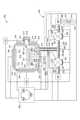
[00019]図1は、処理チャンバ100内の基板400上に配置された材料層をエッチングするのに適した例示的な処理チャンバ100の簡略化された断面図である。例示的な処理チャンバ100は、パターニングプロセスを実行するのに適している。本開示から恩恵を受けるように適合され得る処理チャンバ100の1つの例は、カリフォルニア州サンタクララのApplied Materials, Inc.から入手可能なMESA(登録商標)エッチング処理チャンバである。本開示の実施形態を実施するために、他の製造業者の処理チャンバを含む他の処理チャンバを適合させてもよいと考えられている。 FIG. 1 is a simplified cross-sectional view of an
[00020]プラズマ処理チャンバ100は、チャンバ本体105を含む。チャンバ本体105の内部には、チャンバ空間101が画定されている。チャンバ本体105は、側壁112及び底部118を有し、これらは接地126に連結される。側壁112は、側壁112を保護するためのライナ115を有し、プラズマ処理チャンバ100の保守サイクル間の時間を延ばす。チャンバ本体105及びプラズマ処理チャンバ100の関連構成要素の寸法は限定的なものではなく、通常、その中で処理される基板400のサイズに比例してより大きい。基板サイズの例としては、とりわけ、直径200mm、直径250mm、直径300mm、及び直径450mmのものが含まれる。 [00002] The
[00021]チャンバ本体105は、チャンバリッドアセンブリ110を支持し、それにより、チャンバ空間101を取り囲む。チャンバ本体105はアルミニウム又は他の適切な材料から作製され得る。チャンバ本体105の側壁112を貫通して基板アクセスポート113が形成されており、これがプラズマ処理チャンバ100内外への基板400の移送を容易にする。アクセスポート113は、移送チャンバ及び/又は基板処理システム(図示せず)の他のチャンバに連結されてよい。 [00021] The
[00022]チャンバ本体105の側壁112を貫通してポンピングポート145が形成され、チャンバ空間101に接続される。ポンピングデバイス(図示せず)は、ポンピングポート145を介してチャンバ空間101に連結され、チャンバ空間101の内部を排気し圧力制御する。ポンピングデバイスは、一以上のポンプ及びスロットルバルブを含み得る。 [00022] A pumping
[00023]ガスパネル160は、処理ガスをチャンバ空間101内に供給するために、ガスライン167によってチャンバ本体105に連結される。ガスパネル160は、一以上の処理ガス源161、162、163、164を含み得、所望された場合、不活性ガス、非反応性ガス、及び反応性ガスを追加的に含み得る。ガスパネル160によって供給され得る処理ガスの例には、メタン(CH4)、六フッ化硫黄(SF6)、塩化ケイ素(SiCl4)、四フッ化炭素(CF4)、臭化水素(HBr)、炭化水素含有ガス、アルゴンガス(Ar)、塩素(Cl2)、窒素(N2)、ヘリウム(He)、及び酸素ガス(O2)を含む、炭化水素含有ガスが含まれるが、これに限定されない。加えて、処理ガスには、窒素、塩素、フッ素、酸素、及び水素含有ガス(例えば、とりわけ、BCl3、C2F4、C4F8、C4F6、CHF3、CH2F2、CH3F、NF3、NH3、CO2、SO2、CO、N2,、NO2、N2O、及びH2)が含まれ得る。[00023] The
[00024]バルブ166は、ガスパネル160のソース161、162、163、164からの処理ガスの流れを制御し、コントローラ165によって管理される。ガスパネル160からチャンバ本体105に供給されるガスの流れは、ガスの組み合わせを含み得る。 [00024] The
[00025]リッドアセンブリ110はノズル114を含み得る。ノズル114は、ガスパネル160のソース161、162、164、163からの処理ガスをチャンバ空間101に導入するための一以上のポートを有する。処理ガスがプラズマ処理チャンバ100に導入された後、ガスが活性化されて、プラズマが形成される。一以上のインダクタコイルなどのアンテナ148は、プラズマ処理チャンバ100に隣接して設けられ得る。アンテナ電源142は、整合回路141を介してアンテナ148に給電し、処理ガスにエネルギー(例えばRFエネルギー)を誘導結合し、処理ガスから形成されたプラズマをプラズマ処理チャンバ100のチャンバ空間101内に維持し得る。アンテナ電源142に代えて、又は追加して、基板400の下方及び/又は基板400の上方の処理電極を使用して、処理ガスにRF電力を容量結合して、チャンバ空間101内にプラズマを維持することができる。電源142の動作は、プラズマ処理チャンバ100内の他の構成要素の動作も制御するコントローラ(例えばコントローラ165)によって制御され得る。 The
[00026]基板支持ペデスタル135はチャンバ空間101内に配設され、処理中に基板400を支持する。基板支持ペデスタル135は、処理中に基板400を保持するための静電チャック122を含み得る。静電チャック(electrostatic chuck:ESC)122は、静電引力を利用して、基板400を基板支持ペデスタル135に対して保持する。ESC122は、整合回路124と一体化したRF電源125によって給電される。ESC122は、誘電体内に埋め込まれた電極121を備える。電極121はRF電源125に連結され、バイアスを加える。このバイアスは、チャンバ空間101内の処理ガスによって形成されたプラズマイオンを、ESC122とその上に位置付けられた基板400に引き寄せる。RF電源125は、基板400の処理中にオンとオフを繰り返すか、又はパルスを発し得る。ESC122は、ESC122の保守寿命を延ばすため、ESC122の側壁がプラズマに引き寄せられにくくするための絶縁部128を有する。加えて、基板支持ペデスタル135は、プラズマガスから基板支持ペデスタル135の側壁を保護し、プラズマ処理チャンバ100の保守間隔を延ばすカソードライナ136を有し得る。 [00026] The
[00027]さらに、電極121は、電源150に連結されている。電源150は、約200ボルトから約2000ボルトのチャッキング電圧を電極121に加える。電源150はまた、基板400をチャック及びデチャックするためのDC電流を電極121へ導くことによって電極121の動作を制御するためのシステムコントローラを含み得る。 [00027] Further, the
[00028]ESC122は、基板を加熱するために、ESC122の内部に配設され、電源(図示せず)に接続されたヒータを含み得る。一方、ESC122を支持する冷却ベース129は、ESC122とその上に配設された基板400の温度を維持するために、熱伝導流体を循環させるための導管を含み得る。ESC122は、基板400上に製造されるデバイスの熱収支で要求される温度範囲内で稼働するように構成されている。例えば、ある実施形態では、ESC122は、約-25℃から約500℃の温度で基板400を維持するように構成され得る。 The
[00029]冷却ベース129は、基板400の温度制御を支援するために設けられる。プロセスのドリフトと時間を緩和するため、基板400の温度は、基板400が洗浄チャンバ内にある間中、冷却ベース129によってほぼ一定に維持され得る。一実施形態では、基板400の温度は、後続の洗浄プロセスの間中、約30℃から120℃に維持される。 [0209] The
[00030]カバーリング130はESC122上に、また、基板支持ペデスタル135の周縁に沿って、配設される。カバーリング130は、基板400の露出した上面の所望の部分にエッチングガスを封じ込めながらも、基板支持ペデスタル135の上面をプラズマ処理チャンバ100の内側のプラズマ環境から遮蔽するように構成されている。基板400を基板支持ペデスタル135の上方に持ち上げて、移送ロボット(図示せず)又はその他の適切な移送機構による基板400へのアクセスを容易にするために、リフトピン(図示せず)は、基板支持ペデスタル135を介して選択的に移動させられる。 [000030] The covering 130 is disposed on the
[00031]コントローラ165は、処理シーケンスを制御し、ガスパネル160からプラズマ処理チャンバ100へのガス流及び他の処理パラメータを調整するように利用され得る。ソフトウェアルーチンは、CPUによって実行されると、プラズマ処理チャンバ100を制御する特定目的のコンピュータ(コントローラ)にCPUを変換し、その結果、本開示にしたがってプロセスが実行される。ソフトウェアルーチンはまた、プラズマ処理チャンバ100と一緒に配置される第2のコントローラ(図示せず)によって格納及び/又は実行されてもよい。 The
[00032]図2は、単一の基板400の高圧アニーリングプロセスのための単一基板処理チャンバ200の簡略化された正面断面図である。単一基板処理チャンバ200は、本体210を有し、本体210は、内部空間215を取り囲む外表面212と内表面213とを有する。図2などの幾つかの実施形態では、本体210は環状断面を有するが、他の実施形態では、本体210の断面は長方形又は任意の閉鎖形状になり得る。本体210の外表面212は、例えば限定するものではないが、ステンレス鋼などの耐食鋼(corrosion resistant steel :CRS)から作製され得る。一以上の遮熱材225が、本体210の内表面213に載置されており、単一基板処理チャンバ200から外部環境への熱損失を防止する。本体210の内表面213、及び遮熱材225は、例えば限定するものではないが、HASTELLOY(登録商標)、ICONEL(登録商標)、及びMONEL(登録商標)などの腐食に対して高い耐性を示すニッケル合金鋼から作製され得る。 FIG. 2 is a simplified front sectional view of a single
[00033]基板支持体230が、内部空間215内に配置される。基板支持体230は、脚部234と脚部234により保持された基板支持部材232とを有する。脚部234は、チャンバ本体210を貫通して形成された通路222を通過する。アクチュエータ238に接続されたロッド239が、チャンバ本体210を貫通して形成された第2の通路223を通過する。ロッド239は、プレート235に連結されており、プレート235は、基板支持体230の脚部234を収容する開孔236を有している。リフトピン237が、基板支持部材232に接続されている。リフトピン237と接続又はリフトピン237から切断するために、プレート235が上下に動かされるように、アクチュエータ238はロッド239を作動させる。リフトピン237が上げられ又は下げられるとき、基板支持部材232が、チャンバ200の内部空間215の中で上げられ又は下げられる。基板支持部材232は、その中央に抵抗加熱素子231が埋め込まれている。電源233が、抵抗加熱素子231に電気を供給するよう構成されている。電源233及びアクチュエータ238の動作は、コントローラ280によって制御される。 The
[00034]単一基板処理チャンバ200は、本体210に開口部211を有している。一以上の基板400が、開口部211を通って、内部空間215の中に配置された基板支持体230にロードされ、かつ基板支持体230からアンロードされ得る。開口部211は、本体210にトンネル部221を形成する。スリットバルブ228は、スリットバルブ228が開いているときには開口部211及び内部空間215のみにアクセスし得るように、トンネル部221をシール可能に閉鎖するよう構成される。高圧シール部227は、スリットバルブ228を本体210に対してシールするために利用され、従って、処理のために内部空間215がシールされる。高圧シール部227は、ポリマーから作製され、例えば限定するものではないが、ペルフルオロエラストマー及びポリテトラフルオロエチレン(PTFE)といったフルオロポリマーから作製され得る。高圧シール部227は、シーリング性能を改善するためにシール部を付勢するバネ部材をさらに含み得る。冷却チャネル224が、高圧シール部227の近傍のトンネル部221に配置されており、これにより、処理中に、高圧シール部227が、その最大安全動作温度を下回る温度で維持される。例えば限定するものではないが、不活性かつ誘電性で、高性能の熱伝導流体といった、冷却流体源226からの冷却剤が、冷却チャネル224の内部で循環させられ得る。冷却流体源226からの冷却剤の流れが、温度センサ216又は流量センサ(図示せず)から受信されるフィードバックを通じて、コントローラ280によって制御される。環状形状の熱チョーク229が、トンネル部221の周りに形成されており、スリットバルブ228が開いているときには、内部空間215から熱流が開口部211を通ることが防止される。 The single
[00035]単一基板処理チャンバ200は、本体210を貫通するポート217を有しており、ポート217は、ガスパネル250、コンデンサ260、及びポート217を接続する流体回路290に流体連結されている。流体回路290は、ガス導管292、ソース導管257、入口遮断バルブ255、排気導管263、及び出口遮断バルブ265を有する。複数のヒータ296、258、252、254,264、266が、流体回路290の様々な部分と連結(連動)している。複数の温度センサ251、253、219、267、及び269も、温度測定値を収集してその情報をコントローラ280に送るために、流体回路290の様々な部分に配置されている。コントローラ280は、温度測定情報を使用して、ヒータ252、254、258、296、264、及び266の動作を制御し、流体回路290の温度を、流体回路290及び内部空間215内に配置された処理流体の凝縮点を上回る温度に維持する。 The single
[00036]ガスパネル250は、圧力下で処理流体を内部空間215に供給するように構成される。内部空間215の中に導入される処理流体の圧力は、本体210に連結された圧力センサ214によって監視される。コンデンサ260は、冷却流体源(図示せず)に流体連結され、ガス導管292を通って内部空間215を出る気相の処理流体を凝縮させるよう構成されている。次いで、凝縮された処理流体が、ポンプ276によって取り除かれる。一以上のヒータ240が、本体210に載置されており、単一基板処理チャンバ200の中の内部空間215を加熱するよう構成されている。ヒータ240、252、254、258、296、264、及び266が、流体回路290内の処理流体を気相で維持し、一方、コンデンサ260への出口遮断バルブ265が、流体回路の中での凝縮を防止するために開けられる。 The
[00037]コントローラ280は、単一基板処理チャンバ200の動作を制御する。コントローラ280は、ガスパネル250、コンデンサ260、ポンプ270、入口遮断バルブ255、出口遮断バルブ265、並びに電源233及び245の動作を制御する。コントローラ280はさらに、温度センサ216、圧力センサ214、アクチュエータ238、冷却流体源226、並びに温度読み出しデバイス256及び262と通信可能に接続されている。 The
[00038]処理流体は、酸素含有及び/若しくは窒素含有ガス、並びに/又はカルコゲン若しくはテルリウム(例えば、S、Se、Te)ガス又は蒸気(例えば、酸素、乾燥蒸気、水、過酸化水素、アンモニア、S蒸気、Se蒸気、H2S、H2Se等)を含み得る。処理流体は、基板上の金属材料と反応して、金属酸素窒化物、金属酸化物、金属オキシカルコゲニド、又は金属カルコゲニドを形成し得る。処理流体は、酸素含有ガス及び/又は窒素含有ガスに代えて又は加えて、ケイ素含有ガスを含み得る。ケイ素含有ガスの例は、有機ケイ素ガス、テトラアルキルオルソシリケートガス、及びジシロキサンを含む。有機ケイ素ガスは、少なくとも1つの炭素-ケイ素結合を有する有機化合物のガスを含む。オルトケイ酸テトラアルキルガスは、SiO44ーイオンに付着した4つのアルキル基から成るガスを含む。より具体的には、一以上のガスは、(ジメチルシリル)(トリメチルシリル)メタン((Me)3SiCH2SiH(Me)2)、ヘキサメチルジシラン((Me)3SiSi(Me)3)、トリメチルシラン((Me)3SiH)、トリメチルシリルクロライド((Me)3SiCl)、テトラメチルシラン((Me)4Si)、テトラエトキシシラン((EtO)4Si)、テトラメトキシシラン((MeO)4Si)、テトラキス-(トリメチルシリル)シラン((Me3Si)4Si)、(ジメチルアミノ)ジメチル-シラン((Me2N)SiHMe2)、ジメチルジエトキシシラン((EtO)2Si(Me)2)、ジメチル-ジメトキシシラン((MeO)2Si(Me)2)、メチルトリメトキシシラン((MeO)3Si(Me))、ジメトキシテトラメチル-ジシロキサン(((Me)2Si(OMe))2O)、トリス(ジメチルアミノ)シラン((Me2N)3SiH)、ビス(ジメチルアミノ)メチルシラン((Me2N)2CH3SiH)、ジシロキサン((SiH3)2O)、及びこれらの組み合わせであり得る。The treatment fluid is an oxygen-containing and / or nitrogen-containing gas, and / or a chalcogen or tellurium (eg, S, Se, Te) gas or steam (eg, oxygen, dry steam, water, hydrogen, hydrogen, ammonia, etc.). S steam, Se steam, H2 S, H2 Se, etc.) may be included. The treatment fluid can react with the metallic material on the substrate to form metallic oxygen nitrides, metal oxides, metallic oxychalcogenides, or metallic chalcogenides. The treatment fluid may contain a silicon-containing gas in place of or in addition to the oxygen-containing gas and / or the nitrogen-containing gas. Examples of silicon-containing gases include organosilicon gas, tetraalkyl orthosilicate gas, and disiloxane. The organosilicon gas comprises a gas of an organic compound having at least one carbon-silicon bond. The tetraalkyl orthosilicate gas contains a gas consisting offour alkyl groups attached to SiO444 -ions. More specifically, one or more gases are (dimethylsilyl) (trimethylsilyl) methane ((Me)3 SiCH2 SiH (Me)2 ), hexamethyldisilane ((Me)3 SiSi (Me)3 ), trimethyl. Silane ((Me)3 SiH), trimethylsilyl chloride ((Me)3 SiCl), tetramethylsilane ((Me)4 Si), tetraethoxysilane ((EtO)4 Si), tetramethoxysilane ((MeO)4 Si). ), Tetraxyl- (trimethylsilyl) silane ((Me3 Si)4 Si), (dimethylamino) dimethyl-silane ((Me2 N) SiHMe2 ), dimethyldiethoxysilane ((EtO)2 Si (Me)2 ). , Dimethyl-dimethoxysilane ((MeO)2 Si (Me)2 ), Methyltrimethoxysilane ((MeO)3 Si (Me)), Dimethoxytetramethyl-disiloxane (((Me)2 Si (OME))2 ) O), tris (dimethylamino) silane ((Me2 N)3 SiH), bis (dimethylamino) methylsilane ((Me2 N)2 CH3 SiH), disiloxane ((SiH3 )2 O), and these. Can be a combination of.
[00039]基板400の処理中、内部空間215の環境は、高圧領域内の処理流体が気相に維持される温度及び圧力に、維持される。かかる圧力及び温度は、処理流体の組成に基づいて選択される。蒸気の場合、温度及び圧力は、蒸気を乾燥蒸気状態に維持する状態に保持される。一実施例では、内部空間215は、気圧を上回る(例えば約2barを上回る)圧力まで加圧される。別の実施例では、内部空間215は、約10から約50bar(例えば約20から約50bar)の圧力まで加圧される。別の実施例では、内部空間215は、最大で約100barの圧力まで加圧される。処理中に、内部空間215はまた、高温(基板支持部材132に配置された基板400の熱収支によって制限されるが、例えば、約300℃から約500℃といった、225℃を超える温度)に維持される。 During the processing of the
[00040]図3は、基板上に構造体を形成するために利用される膜積層体における材料層(又は導電層と呼ばれる)をエッチングするためのエッチングプロセスのための方法300の一例のフロー図である。材料層は、膜積層体内に配置された近くの材料とは異なる膜特性を有し得る。図4A~図4B、図5A~図5B、図6A~図6B、図7A~図7B、図8A~図8B、図9A~図9B、及び図10A~図10Bは、方法300の様々な段階に対応する、膜積層体450が上部に形成された基板400一部の斜視図及び断面図である。「A」の記号表示で終わる図は、処理の様々な例における斜視図を示す。「B」の記号表示で終わる図は、断面A-A’に対応する処理の様々な例における断面図を示す。幾つかの図では、他の構成要素又はフィーチャを不明瞭にすることを避けるために、図に示される構成要素又はフィーチャの幾つかの参照番号は省略され得、これは、図を描くことを容易にするためである。方法300は、先進的な半導体用途のために、デュアルダマシン構造体などのバックエンド構造体を形成するために利用され得る。 [00004] FIG. 3 is a flow chart of an example of a
[00041]方法300は、動作302で開始する。動作302では、膜積層体450が上部に形成された基板400を設ける。膜積層体450は、基板400と膜積層体450との間に配置された界面層402を含む。一実施形態では、界面層402は、膜積層体450と基板400との間を埋めることができる任意の適切な材料であり得る。幾つかの実施例では、界面層402は、その上に形成される種々の構造体(例えば、必要に応じてそこに形成されるフロントエンド構造体、バックエンド構造体、コンタクト構造体、金属導電構造体、絶縁構造体等)を含んでもよい。界面層402は、必要に応じて導電層であっても、誘電体層であってもよい。膜積層体450が基板400に対して良好な界面接着性を有する幾つかの実施形態では、界面層402をなくしてもよい。 [00041]
[00042]膜積層体450は、第1の導電層404、第2の導電層406、第3の導電層408、及び第4の導電層410を含む。第1の導電層及び第3の導電層404、408は、類似の材料又は同じ材料によって作製されてもよく、一方、第2の導電層及び第4の導電層406、410は、類似の材料又は同じ材料によって作製されてもよい。言い換えると、第3の導電層及び第4の導電層408、410は、第1の導電層及び第2の導電層404、406のペア(対)の繰り返しである。図4A~図4Bには、2対の導電層のみが示されているが、導電層404、406又は408、410のペアは、必要に応じて任意の数で形成され得ることに留意されたい。一実施例において、第1の導電層及び第3の導電層404、408は、Ru含有層、Mo含有層、NiSi含有層等であり、第2の導電層及び第4の導電層406、410は、Ti含有層、Ta含有層、TiN含有層、TaN含有層、TiON含有層、TaON含有層、TiO含有層、TiN含有層等である。導電層404、406、408、410は、MOCVDプロセス、PECVD、流動性CVD、PVD、ALD、又は任意の適切な堆積技法によって形成され得る。 The
[00043]次いで、誘電体層412が、第4の導電層410上に形成される。誘電体層412は、必要に応じて、酸化ケイ素、窒化ケイ素、酸窒化ケイ素(SiON)、酸炭化ケイ素(SiOC)、又はアモルファス炭素材料であってもよい。次いで、パターニングされたフォトレジスト層416とともに第1の犠牲層414が、誘電体層412上に形成される。第1の犠牲層414は、誘電体層412上にスピンオン塗布された有機ポリマー材料であってもよい。第1の犠牲層414は、炭化水素化合物によって構成される有機ポリマー材料であってもよい。モノマー又はポリマー材料は、式CxHyOz(式中、x、y及びzは整数である)を有し得る。 Next, the
[00044]第1の犠牲層414は、第1の犠牲層414のためのほぼ平坦な上面を生み出すのに十分な厚さで、非平坦な基板表面上にスピンオン塗布されてもよい。図4A~図4Bに示された実施形態では、第1の犠牲層414は、パターニングの準備が整った誘電体層412のほぼ平坦な表面上にスピンオン塗布される。第1の犠牲層414の適切な実施例は、フォトレジスト材料、スピンオンガラス(SOG)材料等を含む。一実施例では、フォトレジスト材料は、ポジ調フォトレジスト、ネガ調フォトレジスト、UVリソグラフィフォトレジスト、I線フォトレジスト、G線フォトレジスト、電子ビームレジスト(例えば、化学的増幅型レジスト(CAR))、又は他の適切なフォトレジストであってもよい。第1の犠牲層414に提供される有機ポリマー材料は、基板上に形成される構造体の不均一なトポグラフィ(もしあれば)を均一に覆うように誘電体層412上に被覆されるように、セルフレベリング性の平坦化特性を有し得ると考えられている。そうすることによって、基板400からの不均一なトポグラフィック表面は、平坦化又は扁平化された上面で覆われて、後続のフォトリソグラフィプロセスが容易となり、正確かつ精密な寸法制御で、フィーチャが基板400上の膜積層体450内に転写される。 The first
[00045]一実施形態では、第1の犠牲層414は、基板表面上にスピンコーティングされてもよい。別の実施形態では、第1の犠牲層414はまた、必要に応じて、注入、噴霧堆積システム、エアゾール堆積(AD)プロセス、エアロジェット、溶液からのナノ粒子噴霧、噴霧CVD、インクジェット、メニスカスコーティング、浸漬コーティング、電気めっき、噴霧コーティング、電気スプレー、スクリーン印刷、又は他の適切な技法を使用して、基板上に被覆されてもよい。 [00045] In one embodiment, the first
[00046]パターニングされたフォトレジスト層416は、有機レジスト層を含む。パターニングされたフォトレジスト層416は、必要に応じて極紫外線(EUV)用途に利用され得る。 The patterned
[00047]動作304では、第1のエッチングプロセスが実行されて、パターニングされたフォトレジスト層416をエッチングマスクとして使用して、膜積層体450をパターニングする。第1のエッチングプロセスは、図5A及び図5Bに示されるように、第2の導電層406が露出するまで、膜積層体450をエッチングするために実行され、膜積層体450から、パターニングされた構造体432(さらに、432a、432bとして示される)の間で膜積層体450において開口領域430を形成する。エッチングプロセスは、基板400を、エッチング処理チャンバ(例えば、図1に示された処理チャンバ100)内に移送することによって実行され得る。第1のエッチングプロセスは、第1の犠牲層414、誘電体層412、第4の導電層410、及び第3の導電層408を効率的な方式でエッチングするように、エッチングプロセスの異なる段階中に供給される複数の種々のエッチング前駆体を有し得る。一実施例では、膜積層体450をエッチングするために利用されるエッチング前駆体は、ハロゲン含有ガス等を含む。エッチング前駆体の適切な例としては、CH4、C2H6、C4H8、C4F6、C4F8、C2F2、CF4、CHF3、C2F6、C4F6、C5F8、CH2F2、SF6、NF3、Cl2、HBr、HCl、HF等が含まれる。O2、O2、H2、N2、H2O、O3、CO2等の他の反応ガスも、必要に応じてエッチングプロセス中に供給され得る。In
[00048]膜積層体450の所定の部分(例えば開口領域430)がエッチングされた後、次いで、第2の犠牲層422が、図6A~図6Bに示されるように、第2のパターニングされたフォトレジスト層438と同様に、膜積層体450上に形成される。第2のパターニングされたフォトレジスト層438は、パターニングされた構造体432の上方に形成され、それぞれ、パターニングされた構造体432の2つの端部と垂直に整列される。第2のパターニングされたフォトレジスト層438は、パターニングされた構造体432(図7A~図7B及び図8A~図8Bにさらに示される)の中心部分440を露光する。構造体432は、以下のエッチングプロセスでパターニングされる。 After a predetermined portion of the film laminate 450 (eg, opening region 430) was etched, a second
[00049]第2の犠牲層422は、第1の犠牲層414と類似又は同じである。第2の犠牲層422は、第2の犠牲層422のためのほぼ平坦な上面を生み出すのに十分な厚さで、非平坦な基板表面上に形成される。図5A~図5Bに先に示されるように、エッチングプロセスの後、開口領域430が、パターニングされた構造体432(さらに、432a、432bとして示される)の間に形成され、したがって、不均一な表面が生み出される。したがって、第2の犠牲層422は、セルフレベリング能力を有しており、エッチングされた膜積層体450の不均一な表面上に被覆され、不均一なトポグラフィーを均一に覆う。そうすることにより、パターニングされた構造体432の間の開口領域430からの不均一なトポグラフィック表面は、平坦化又は扁平化された上面で覆われ、後続のフォトリソグラフィプロセスを容易にし得る。 The second
[00050]第2の犠牲層422が形成された後、第2のエッチングプロセスが実行されて、基板400上に形成された第2のパターニングされたフォトレジスト層438の間に画定された開口領域430及び中心部分440を通して、膜積層体450をエッチングする。第2のエッチングプロセスは、図7A~図7Bに示されるように、第4の導電層410の表面441a、441bが露出するまで連続的に実行される。第4の導電層410の表面441a、441bは、第2のパターニングされたフォトレジスト層438によって画定された中心部分440と整列し、その結果、第2のエッチングプロセスの後に、中心部分440によって露出された第4の導電層410の表面441a、441bが次いで露出されることに留意されたい。次いで、パターニングされた構造体432a、432bは、中心部分440からそれぞれ表面441a、441bを含むようにさらにエッチングされ、表面441a、441bによって接続されたコーナー構造体432c、432d、432e、432fを形成する。図7A~図7Bに示された構造体では、誘電体層412の側壁445が露出され、また、中心部分440における第3及び第4の導電層408、410の側壁442a、442bが露出される。 [000050] After the second
[00051]動作306では、残留物除去プロセスが実行されて、残りの第2の犠牲層422が基板400から取り除かれ、図8A~図8Bに示されるように、開口領域430内の第2の導電層406が露出する。残留物除去プロセスは、基板400から残留物第2の犠牲層422を取り除くために実行される。第4の導電層410上の残留第2の犠牲層422と、中心部分440及び開口領域430における第2の導電層406は、第4の導電層410及び第2の導電層406を取り除くために続いて実行されるエッチングの性能に悪影響を及ぼす恐れがある。したがって、第2及び第4の導電層406、410が取り除かれる前に、残留物除去プロセスが実行される。 In operation 306, a residue removal process is performed to remove the remaining second
[00052]一実施例では、残留物除去プロセスは水素処理プロセスである。残留物除去プロセスは、水素含有ガスを含む残留物除去混合ガスを基板400に供給して、図8A~図8Bに示すように、第2及び第4の導電層410、408の中央部分440及び開口領域430が露出するまで、基板400から残留第2の犠牲層422(図7A~図7Bに示す)を取り除くことによって実行される。残留物除去混合ガスは、水素含有ガス及び任意選択的に不活性ガスを含む。水素含有ガスの適切な例には、H2、H2O、H2O2、NH3等が含まれる。[00052] In one embodiment, the residue removal process is a hydrogen treatment process. In the residue removal process, a residue removal mixed gas containing a hydrogen-containing gas is supplied to the
[00053]残留物除去プロセスを実行する間、種々の材料を有する露出表面(例えば、図7A~図7Bに示すように、第4の導電層410の中央部分440の表面441a、441b、第3の導電層408の側壁442a、442b、及び誘電体層412の側壁445)の幾つかも、残留物除去混合ガスからの反応種の下で露出される。したがって、残留物除去プロセスを実行するための反応種は、これらの材料間で高い選択性を有するように選択され、その結果、反応種は、露出した第4の導電層410、第3の導電層408、及び誘電体層412を実質的に付着させることなく、残留第2の犠牲層422を選択的に取り除くことができる。一実施形態では、遠隔プラズマ源から供給される水素含有ガスが、残留第2の犠牲層422を選択的に取り除くために供給される。窒素含有ガス(例えば、N2、N2O、NO2、NH3)も、残留物除去混合ガス中に任意選択的に供給され得る。特定の一実施例では、残留物除去混合ガスは、H2及びN2を含む。[00053]
[00054]残留物除去プロセスにおいては、幾つかの処理パラメータも調整され得る。例示的な一実施形態では、処理チャンバ100内の処理圧力は、約10mTorrから約5000mTorr(例えば、約10mTorrから約200mTorr)に調整される。遠隔プラズマ源及び/又は任意選択のRFバイアス電力は、残留物除去プロセスによって利用してもよい。遠隔プラズマ源に供給される電力は、1000ワットから約20000ワット(例えば約5000ワット)であってもよい。一実施例では、残留物除去混合ガスが供給されている間、RFバイアス電力は印加されない。残留物除去プロセスを実行しつつRFバイアス電力を除去することは、残留物除去混合ガスから生成されたプラズマ中の反応種が、特定の方向性なしに比較的弱い電力で基板表面にわたってより均一に分配されるのを支援し得る。 In the residue removal process, some processing parameters may also be adjusted. In one exemplary embodiment, the processing pressure in the
[00055]残留物除去混合ガスからの水素含有ガスは、体積比で約500sccmから約2000sccmの間の速度でチャンバに流入され得、窒素含有ガスは、体積比で約500sccmから約2000sccmの間の速度で供給され得る。残留物除去混合ガスからの炭化水素含有ガス及び窒素含有ガスは、処理チャンバに同時に供給されてもよく、あるいは、必要に応じて代替的に又は連続的に供給されてもよい。 Hydrogen-containing gas from the residue-removing mixed gas may flow into the chamber at a rate of between about 500 sccm and about 2000 sccm by volume, and nitrogen-containing gas may be between about 500 sccm and about 2000 sccm by volume. Can be supplied at speed. The hydrocarbon-containing gas and the nitrogen-containing gas from the residue-removing mixed gas may be supplied to the processing chamber simultaneously, or may be supplied alternately or continuously as required.
[00056]基板温度は、100℃を上回る温度(例えば、約120℃から約400℃、約150℃から約350℃、約200℃から約300℃)に維持される。残留物除去プロセス中の基板400の高温制御は、基板400上の他の材料に損傷を与えることなく、除去効率を向上させるように、残留第2の犠牲層422からポリマー材料を蒸発させることを支援し得ると考えられている。 The substrate temperature is maintained above 100 ° C. (eg, from about 120 ° C to about 400 ° C, from about 150 ° C to about 350 ° C, from about 200 ° C to about 300 ° C). The high temperature control of the
[00057]動作308では、主エッチングプロセスが実行されて、図9A~図9Bに示されるように、下層の第3及び第1の導電層408、404が露出するまで、露出した第4及び第2の導電層410、406を同時にエッチングする。主エッチングプロセスは、露出した第4及び第2の導電層410、406をエッチングするために、図1に示された処理チャンバ100などの処理チャンバに主エッチング混合ガスを供給することによって実行される。 In
[00058]主エッチングプロセスは、ブレイクスループロセス、バルクエッチングプロセス、及び残留物洗浄プロセスを含む3つのステップをさらに含む。実行される主エッチングプロセスは、選択性が高く、主エッチングプロセスからの反応種は、誘電体層412並びに下層の第3及び第1の導電層408、404を、露出されたときに実質的に浸食することなく、第4及び第2の導電層410、406を主としてエッチングすることができる。第4及び第2の導電層410、406がチタン(Ti)含有材料である実施例では、主エッチング混合ガスからの反応種は、誘電体層412からの酸化物材料と実質的に反応することなく、主としてチタン(Ti)含有材料と反応することができ、したがって選択的エッチングプロセスを実現する。選択的エッチングプロセスは、近傍の材料(例えば、この実施例では誘電体層412からの酸化物含有材料)を浸食又は損傷することなく、ターゲット材料(例えば、この実施例ではチタン(Ti)含有材料)を優先的にエッチングし得る。 The main etching process further comprises three steps including a breakthrough process, a bulk etching process, and a residue cleaning process. The main etching process performed is highly selective and the reaction species from the main etching process are substantially when the
[00059]一実施例では、主エッチング混合ガスは、塩素含有ガスなどのハロゲン含有ガスである。主エッチング混合ガス中に不活性ガスも供給され得る。塩素含有ガスの適切な例には、Cl2、HCl等が含まれる。塩素含有ガスは、誘電体層412からの酸化物損傷又は酸化物損失を最小限に抑えるように、第4及び第2の導電層410、406からのTi又はTa元素と主として反応し得ると考えられている。一実施例では、主エッチング混合ガスには、Cl2ガスなどの塩素含有ガス、及びArガスが含まれる。In one embodiment, the main etching mixed gas is a halogen-containing gas such as a chlorine-containing gas. An inert gas may also be supplied into the main etching mixed gas. Suitable examples of chlorine-containing gases include Cl2 , HCl and the like. It is believed that the chlorine-containing gas can react primarily with Ti or Ta elements from the fourth and second
[00060]一実施例では、主エッチング混合ガス中に供給されるCl2ガスとArガスとの比率は、チタン(Ti)含有材料をエッチングする間に、改変、調節、変更、又は変化してもよい。チタン(Ti)含有材料の上面がしばしばTiOxを含むので、主エッチング混合ガス中でCl2ガスが比較的高い比率(例えば、より高い塩素ガスの流量)を有することを利用して、第4及び第2の導電層410、406からのチタン(Ti)含有材料の表面から表面酸化物(もしあれば)をブレイクスルーする。一実施例では、上部TiOxの厚さは、第4及び第2の導電層410、406の全厚さの約3%及び約20%であってもよい。一実施例では、主エッチング混合ガス中に供給されるCl2ガスは、ブレイクスループロセス中に主エッチング混合ガス中に供給されるArガスに対して高い比率を有する。一実施例では、主エッチング混合ガス中に供給されるCl2ガスとArガスは、約10:1から約50:1などの、10:1よりも大きい比(Cl2ガス:Arガス)で制御される。主混合ガス中のCl2ガスは、第1の流量で供給される。[00006] In one embodiment, the ratio of Cl2 gas to Ar gas supplied in the main etching mixed gas is modified, adjusted, changed, or changed during etching of the titanium (Ti) -containing material. May be good. Since the upper surface of the titanium (Ti) -containing material often contains TiOx, the fourth and fourth and taking advantage of the relatively high proportion of Cl2 gas in the main etching mixed gas (eg, higher chlorine gas flow rate). The surface oxide (if any) is broken through from the surface of the titanium (Ti) -containing material from the second
[00061]チタン(Ti)含有材料がブレイクスルーされた後、第4及び第2の導電層410、406からチタン(Ti)含有材料のバルク体をエッチング(例えば、又はバルクエッチングプロセスと呼ばれる)するために、比較的同程度の量のCl2ガスとArガス(例えば、より低い塩素ガス流量又は流量比)が、次いで、主エッチング混合ガス中で使用される。バルクチタン(Ti)含有材料エッチングプロセスでは、主エッチング混合ガス中に供給されるCl2ガスとArガスは、約1:4から約2:1の比(Cl2ガス:Arガス)で制御される。この実施例では、第4及び第2の導電層410、406の厚さは、第4及び第2の導電層410、406の全厚さから約5%及び約98%(例えば、約50%から約98%)エッチングされ得る。主混合ガス中のCl2ガスは、第1の流量よりも低いバルクエッチングプロセスで第2の流量で供給される。[00061] After the titanium (Ti) -containing material is broken through, the bulk body of the titanium (Ti) -containing material is etched (for example, referred to as a bulk etching process) from the fourth and second
[00062]最後に、(ブレイクスループロセスと似たような)Arガスに対するCl2ガスの比較的高い比率を使用して、第4及び第2の導電層410、406から残留チタン(Ti)含有材料を取り除き(例えば、又はこれは残留洗浄プロセスと呼ばれる)、誘電体層412から酸化物の残留物(もしあれば)を取り除く。残留物洗浄プロセスにおける主混合ガス中のCl2ガスは、第2の流量よりも少ないが、第1の流量と類似又は同じの第3の流量である。一実施例では、残留物洗浄プロセスにおいて主エッチング混合ガス中に供給されるCl2ガスとArガスは、約10:1と約20:1との間など、10:1よりも大きい比(Cl2ガス:Arガス)で制御される。残留物洗浄プロセス及びブレイクスループロセスのための主エッチング混合ガス中のCl2ガスとArガスの比は、類似又は同じであってもよいことに留意されたい。Finally, the fourth and second
[00063]第4及び第2の導電層410、406をエッチングするために供給される主エッチング混合ガスは、ブレイクスループロセス、バルクエッチングプロセス、及び残留物洗浄プロセスにおける様々な処理要件を満たすように、徐々に調節、変更、又は改変され得ることに留意されたい。 [00063] The main etching mixed gas supplied for etching the fourth and second
[00064]主エッチングプロセス(ブレイクスループロセス、バルクエッチングプロセス、及び残留物洗浄プロセスを含む)において、幾つかの処理パラメータも調整され得る。例示的な一実施形態では、処理チャンバ100内の処理圧力は、約10mTorrから約5000mTorr(例えば、約10mTorrから約200mTorr)に調整される。フラッシュエッチングプロセスを実行する間、RF源及び/又はバイアス電力を利用してもよい。RF源及びRFバイアス電力は、連続モード又はパルスモードで処理チャンバに印加されてもよい。一実施例では、RFバイアス電力は、主エッチング混合ガスを供給している間、印加される。 [00064] In the main etching process (including breakthrough process, bulk etching process, and residue cleaning process), some processing parameters may also be adjusted. In one exemplary embodiment, the processing pressure in the
[00065]主エッチング混合ガスを供給するときに印加されるRFバイアス電力は、エッチングのために第4及び第2の導電層410、406の反応性露出面440a、440b、430を形成するのを支援する。一実施例では、堆積混合ガス内のプラズマを維持するために、約13MHzの周波数のRFソース電力が印加され得る。例えば、処理チャンバ100の内側にプラズマを維持するために、約100ワットから約1000ワットのRFソース電力が印加され得る。主エッチング混合ガスを供給する間、約300ワット及び約700ワットのRFバイアス電力が印加され得る。 The RF bias power applied when supplying the main etching mixed gas forms the reactive exposed
[00066]基板温度は、約10℃から約300℃(例えば、約20℃から約80℃、約30℃から約50℃)に維持される。 The substrate temperature is maintained at about 10 ° C to about 300 ° C (eg, about 20 ° C to about 80 ° C, about 30 ° C to about 50 ° C).
[00067]動作310では、ポストアニーリングプロセスが実行される。ポストアニーリングプロセスは、高い処理圧力(例えば、2bar超70bar未満)で実行される高圧アニーリングプロセスである。高圧アニーリングプロセスは、空孔やエッチング副生成物及び/又は残留物を修復し、主エッチングプロセス後の露出した第3及び第1の導電層408、404並びに誘電体層412において主エッチングプロセスから生じ得る表面粗さを平滑化することを支援することができる。幾つかの実施例では、高い処理圧力は、最大で70barまで上昇し得る。高圧アニーリングプロセスは、図2に示された処理チャンバ200などの処理チャンバ、又は基板を一度に1枚ずつ処理するものを含む他の適切な処理チャンバで実行され得る。 In
[00068]動作310で実行される高圧アニーリングプロセスは、例えば、実質的に液体液滴が存在しない乾燥気相において、気相における高圧領域での処理圧力を維持する。処理圧力及び処理温度は、膜欠陥を修復するように、膜構造を高密度化するように制御され、表面粗さを平滑化する不純物を排出する。一実施例では、内部空間215(図2に示される)は、大気圧を上回る圧力(例えば約2bar超)まで加圧される。別の実施例では、内部空間215は、約5から約70bar(例えば、約5から約50bar、約25barから約55bar)の圧力まで加圧される。高圧は膜構造の高密度化を効率的に支援し得るので、比較的低い処理温度(例えば500℃未満)が、基板400に対する熱サイクル損傷を低減し得る。 The high pressure annealing process performed in
[00069]処理中、内部空間215は、ヒータ240によって、比較的低い温度(例えば、約150℃から約350℃など、500℃を下回る温度)に維持される。したがって、基板への低い熱収支は、低い温度レジームと共に高圧アニーリングプロセスを利用することによって得ることができる。 During the process, the
[00070]高圧プロセスは、露出した第3及び第1の導電層408、404並びに誘電体層412におけるダングリングボンドを排出し、ひいては、残留物を修復し、アニーリングプロセス中、露出した第3及び第1の導電層408、404並びに誘電体層412における表面粗さを平滑化する駆動力をもたらし得ると考えられている。一実施例では、H2、H2O、H2O2、N2O、NO2、NH3、及び乾燥蒸気などの水素又は窒素含有ガスを、アニーリングプロセス中に供給してもよい。また、アニーリングプロセス中に、He及びArなどの不活性ガスを供給してもよい。The high pressure process drains the dangling bonds in the exposed third and first
[00071]例示的な一実施態様では、処理圧力は、2barを上回る圧力(例えば、5barから70bar、20barから約50bar)に調整される。処理温度は、150℃超500℃未満の温度(例えば、約150℃から約380℃、約180℃から約400℃)に制御され得る。 In one exemplary embodiment, the processing pressure is adjusted to a pressure greater than 2 bar (eg, 5 bar to 70 bar, 20 bar to about 50 bar). The treatment temperature can be controlled to a temperature greater than 150 ° C. and less than 500 ° C. (eg, from about 150 ° C to about 380 ° C, from about 180 ° C to about 400 ° C).
[00072]高圧でのアニーリングプロセスの後、第3及び第1の導電層408、404並びに誘電体層412は、表面粗さが滑らかで、純度が高く、大きな粒子構造を有する修復された膜構造を有し、これにより、より高い膜密度を実現する比較的堅牢な膜構造がもたらされ、低い膜抵抗が得られる。第3及び第1の導電層408、404がRu含有材料である実施例では、第3及び第1の導電層408、404からのRu含有材料の膜抵抗は、高圧アニーリングプロセス後に約3%から約7%低下させることができる。 After the annealing process at high pressure, the third and first
[00073]動作312では、第3及び第1の導電層408、404が露出された後、さらなるエッチングプロセスが実行され得、図10A~図10Bに示されるように、所望の構造体460が基板400上に形成されるまで、図9A~図9Bに示されるように、第3及び第1の導電層408、404を取り除き、続いて、追加のエッチングプロセスが実行され得る。基板400上に形成されるような構造体460は、半導体用途のバックエンド構造に利用されるデュアルサブトラクティブ構造(dual subtractive structure)であってもよい。構造体460はまた、必要に応じて基板400上に任意の適切な構造体を形成するのに利用されてもよいことにも留意されたい。 In
[00074]したがって、膜積層体におけるフィーチャをエッチングするための方法が提供される。本方法は、膜積層体における金属含有材料をエッチングするために、残留物除去プロセス、主エッチングプロセス、及び高圧アニーリングプロセスを含む3つのステップ処理を利用する。さらに、主エッチングプロセスは、ブレイクスループロセス、バルクエッチングプロセス、及び残留物洗浄プロセスを含む3つのステップ処理をさらに含む。本プロセスは、膜積層体における他の材料を実質的に浸食することなく、膜積層体における導電層などのターゲット材料を効率的にエッチングすることができる。 [00074] Therefore, a method for etching features in a membrane laminate is provided. The method utilizes a three-step process, including a residue removal process, a main etching process, and a high pressure annealing process, to etch the metal-containing material in the membrane laminate. In addition, the main etching process further comprises a three-step process including a breakthrough process, a bulk etching process, and a residue cleaning process. This process can efficiently etch a target material, such as a conductive layer, in a membrane laminate without substantially eroding other materials in the membrane laminate.
[00075]上記の説明は本開示の実施形態を対象としているが、本開示の基本的な範囲を逸脱しなければ、本開示の他の実施形態及びさらなる実施形態が考案されてよく、本開示の範囲は以下の特許請求の範囲によって決まる。 [00075] The above description is intended for embodiments of the present disclosure, but other embodiments and further embodiments of the present disclosure may be devised as long as they do not deviate from the basic scope of the present disclosure. The scope of is determined by the following claims.
Claims (15)
Translated fromJapanese前記基板上に堆積した第1の導電層をエッチングするために、第1の流量で、塩素含有ガスを含む混合ガスを供給すること、
前記第1の導電層をエッチングし続けるために、前記第1の流量よりも低い第2の流量まで、第1の混合ガスの中の前記塩素含有ガスを低下させること、及び
前記基板から前記第1の導電層を取り除くために、前記第2の流量よりも大きい第3の流量まで、前記第1の混合ガスの中の前記塩素含有ガスを増加させること
を含む、方法。A method for patterning a conductive layer on a substrate.
Supplying a mixed gas containing a chlorine-containing gas at a first flow rate in order to etch the first conductive layer deposited on the substrate.
In order to continue etching the first conductive layer, the chlorine-containing gas in the first mixed gas is lowered to a second flow rate lower than the first flow rate, and the substrate to the first. A method comprising increasing the chlorine-containing gas in the first mixed gas to a third flow rate greater than the second flow rate in order to remove the conductive layer of 1.
Applications Claiming Priority (3)
| Application Number | Priority Date | Filing Date | Title |
|---|---|---|---|
| US201862752764P | 2018-10-30 | 2018-10-30 | |
| US62/752,764 | 2018-10-30 | ||
| PCT/US2019/056447WO2020092002A1 (en) | 2018-10-30 | 2019-10-16 | Methods for etching a structure for semiconductor applications |
Publications (3)
| Publication Number | Publication Date |
|---|---|
| JP2022505863Atrue JP2022505863A (en) | 2022-01-14 |
| JP7179172B2 JP7179172B2 (en) | 2022-11-28 |
| JP7179172B6 JP7179172B6 (en) | 2022-12-16 |
Family
ID=70327214
Family Applications (1)
| Application Number | Title | Priority Date | Filing Date |
|---|---|---|---|
| JP2021522545AActiveJP7179172B6 (en) | 2018-10-30 | 2019-10-16 | Method for etching structures for semiconductor applications |
Country Status (6)
| Country | Link |
|---|---|
| US (1) | US10957533B2 (en) |
| JP (1) | JP7179172B6 (en) |
| KR (1) | KR102528076B1 (en) |
| CN (1) | CN112640065B (en) |
| TW (1) | TWI826555B (en) |
| WO (1) | WO2020092002A1 (en) |
Families Citing this family (15)
| Publication number | Priority date | Publication date | Assignee | Title |
|---|---|---|---|---|
| US10224224B2 (en) | 2017-03-10 | 2019-03-05 | Micromaterials, LLC | High pressure wafer processing systems and related methods |
| US10622214B2 (en) | 2017-05-25 | 2020-04-14 | Applied Materials, Inc. | Tungsten defluorination by high pressure treatment |
| US10276411B2 (en) | 2017-08-18 | 2019-04-30 | Applied Materials, Inc. | High pressure and high temperature anneal chamber |
| WO2019036157A1 (en) | 2017-08-18 | 2019-02-21 | Applied Materials, Inc. | High pressure and high temperature anneal chamber |
| JP7274461B2 (en) | 2017-09-12 | 2023-05-16 | アプライド マテリアルズ インコーポレイテッド | Apparatus and method for manufacturing semiconductor structures using protective barrier layers |
| CN117936420A (en) | 2017-11-11 | 2024-04-26 | 微材料有限责任公司 | Gas delivery system for high pressure processing chamber |
| KR20200075892A (en) | 2017-11-17 | 2020-06-26 | 어플라이드 머티어리얼스, 인코포레이티드 | Condenser system for high pressure treatment systems |
| SG11202008256WA (en) | 2018-03-09 | 2020-09-29 | Applied Materials Inc | High pressure annealing process for metal containing materials |
| US10950429B2 (en) | 2018-05-08 | 2021-03-16 | Applied Materials, Inc. | Methods of forming amorphous carbon hard mask layers and hard mask layers formed therefrom |
| US10748783B2 (en) | 2018-07-25 | 2020-08-18 | Applied Materials, Inc. | Gas delivery module |
| CN109148288A (en)* | 2018-08-16 | 2019-01-04 | 武汉华星光电半导体显示技术有限公司 | The method for making conducting wire |
| WO2020117462A1 (en) | 2018-12-07 | 2020-06-11 | Applied Materials, Inc. | Semiconductor processing system |
| US11508617B2 (en)* | 2019-10-24 | 2022-11-22 | Applied Materials, Inc. | Method of forming interconnect for semiconductor device |
| US11257677B2 (en) | 2020-01-24 | 2022-02-22 | Applied Materials, Inc. | Methods and devices for subtractive self-alignment |
| US11901222B2 (en) | 2020-02-17 | 2024-02-13 | Applied Materials, Inc. | Multi-step process for flowable gap-fill film |
Citations (7)
| Publication number | Priority date | Publication date | Assignee | Title |
|---|---|---|---|---|
| JPH08330275A (en)* | 1995-05-30 | 1996-12-13 | Matsushita Electron Corp | Silicon etching method, and manufacture of ccd solid image pickup device using this method |
| JPH10338515A (en)* | 1997-06-06 | 1998-12-22 | Shin Etsu Chem Co Ltd | Oxidation of silicon substrate |
| US20040074869A1 (en)* | 2002-10-18 | 2004-04-22 | Applied Materials, Inc. | Fluorine free integrated process for etching aluminum including chamber dry clean |
| CN1630042A (en)* | 2003-12-18 | 2005-06-22 | 上海华虹Nec电子有限公司 | Multistep dry process etching method for metal wiring |
| JP2005311148A (en)* | 2004-04-23 | 2005-11-04 | Ishikawajima Harima Heavy Ind Co Ltd | Manufacturing method of semiconductor device |
| JP2008244479A (en)* | 2007-03-23 | 2008-10-09 | Tokyo Electron Ltd | Method and system for dry-etching metal nitride |
| JP2017183490A (en)* | 2016-03-30 | 2017-10-05 | 株式会社日立国際電気 | Semiconductor device manufacturing method, substrate processing apparatus, and program |
Family Cites Families (286)
| Publication number | Priority date | Publication date | Assignee | Title |
|---|---|---|---|---|
| US4524587A (en) | 1967-01-10 | 1985-06-25 | Kantor Frederick W | Rotary thermodynamic apparatus and method |
| JPS634616A (en) | 1986-06-25 | 1988-01-09 | Hitachi Tokyo Electron Co Ltd | Steam treating unit |
| JPH0748489B2 (en) | 1987-07-27 | 1995-05-24 | 富士通株式会社 | Plasma processing device |
| US4879259A (en) | 1987-09-28 | 1989-11-07 | The Board Of Trustees Of The Leland Stanford Junion University | Rapid thermal annealing of gallium arsenide with trimethyl arsenic overpressure |
| US5114513A (en) | 1988-10-27 | 1992-05-19 | Omron Tateisi Electronics Co. | Optical device and manufacturing method thereof |
| JP2730695B2 (en) | 1989-04-10 | 1998-03-25 | 忠弘 大見 | Tungsten film forming equipment |
| US5126117A (en) | 1990-05-22 | 1992-06-30 | Custom Engineered Materials, Inc. | Device for preventing accidental releases of hazardous gases |
| US5175123A (en) | 1990-11-13 | 1992-12-29 | Motorola, Inc. | High-pressure polysilicon encapsulated localized oxidation of silicon |
| US5050540A (en) | 1991-01-29 | 1991-09-24 | Arne Lindberg | Method of gas blanketing a boiler |
| JPH05129296A (en) | 1991-11-05 | 1993-05-25 | Fujitsu Ltd | Method of flatting conductive film |
| US5319212A (en) | 1992-10-07 | 1994-06-07 | Genus, Inc. | Method of monitoring ion beam current in ion implantation apparatus for use in manufacturing semiconductors |
| JPH06283496A (en) | 1993-03-26 | 1994-10-07 | Dainippon Screen Mfg Co Ltd | Dryer of substrate after washing |
| US5607002A (en) | 1993-04-28 | 1997-03-04 | Advanced Delivery & Chemical Systems, Inc. | Chemical refill system for high purity chemicals |
| US5578132A (en) | 1993-07-07 | 1996-11-26 | Tokyo Electron Kabushiki Kaisha | Apparatus for heat treating semiconductors at normal pressure and low pressure |
| US5880041A (en) | 1994-05-27 | 1999-03-09 | Motorola Inc. | Method for forming a dielectric layer using high pressure |
| US5808245A (en) | 1995-01-03 | 1998-09-15 | Donaldson Company, Inc. | Vertical mount catalytic converter muffler |
| US5620524A (en) | 1995-02-27 | 1997-04-15 | Fan; Chiko | Apparatus for fluid delivery in chemical vapor deposition systems |
| KR100251341B1 (en) | 1995-05-08 | 2000-05-01 | 오카노 사다오 | Manufacturing method of optical waveguide |
| JP2872637B2 (en) | 1995-07-10 | 1999-03-17 | アプライド マテリアルズ インコーポレイテッド | Microwave plasma based applicator |
| JP3254997B2 (en)* | 1995-12-25 | 2002-02-12 | ソニー株式会社 | Plasma CVD method and semiconductor device having metal film formed thereby |
| US5895274A (en) | 1996-01-22 | 1999-04-20 | Micron Technology, Inc. | High-pressure anneal process for integrated circuits |
| KR980012044A (en) | 1996-03-01 | 1998-04-30 | 히가시 데츠로 | Substrate drying apparatus and substrate drying method |
| US5998305A (en) | 1996-03-29 | 1999-12-07 | Praxair Technology, Inc. | Removal of carbon from substrate surfaces |
| US5827437A (en)* | 1996-05-17 | 1998-10-27 | Lam Research Corporation | Multi-step metallization etch |
| KR100213207B1 (en)* | 1996-06-29 | 1999-08-02 | 윤종용 | Gate formation method of polyside structure |
| US5738915A (en) | 1996-09-19 | 1998-04-14 | Lambda Technologies, Inc. | Curing polymer layers on semiconductor substrates using variable frequency microwave energy |
| US6444037B1 (en) | 1996-11-13 | 2002-09-03 | Applied Materials, Inc. | Chamber liner for high temperature processing chamber |
| US6082950A (en) | 1996-11-18 | 2000-07-04 | Applied Materials, Inc. | Front end wafer staging with wafer cassette turntables and on-the-fly wafer center finding |
| US6136664A (en) | 1997-08-07 | 2000-10-24 | International Business Machines Corporation | Filling of high aspect ratio trench isolation |
| US20030049372A1 (en) | 1997-08-11 | 2003-03-13 | Cook Robert C. | High rate deposition at low pressures in a small batch reactor |
| US5963817A (en) | 1997-10-16 | 1999-10-05 | International Business Machines Corporation | Bulk and strained silicon on insulator using local selective oxidation |
| JP3199006B2 (en) | 1997-11-18 | 2001-08-13 | 日本電気株式会社 | Method of forming interlayer insulating film and insulating film forming apparatus |
| US6442980B2 (en) | 1997-11-26 | 2002-09-03 | Chart Inc. | Carbon dioxide dry cleaning system |
| US6846739B1 (en) | 1998-02-27 | 2005-01-25 | Micron Technology, Inc. | MOCVD process using ozone as a reactant to deposit a metal oxide barrier layer |
| US6164412A (en) | 1998-04-03 | 2000-12-26 | Arvin Industries, Inc. | Muffler |
| US6719516B2 (en) | 1998-09-28 | 2004-04-13 | Applied Materials, Inc. | Single wafer load lock with internal wafer transport |
| US20030101938A1 (en) | 1998-10-27 | 2003-06-05 | Applied Materials, Inc. | Apparatus for the deposition of high dielectric constant films |
| US6468490B1 (en) | 2000-06-29 | 2002-10-22 | Applied Materials, Inc. | Abatement of fluorine gas from effluent |
| US6612317B2 (en) | 2000-04-18 | 2003-09-02 | S.C. Fluids, Inc | Supercritical fluid delivery and recovery system for semiconductor wafer processing |
| US6334266B1 (en) | 1999-09-20 | 2002-01-01 | S.C. Fluids, Inc. | Supercritical fluid drying system and method of use |
| EP1077477B1 (en) | 1999-08-17 | 2008-12-17 | Applied Materials, Inc. | Surface treatment of C-doped SiO2 film to enhance film stability during O2 ashing |
| US6299753B1 (en) | 1999-09-01 | 2001-10-09 | Applied Materials, Inc. | Double pressure vessel chemical dispenser unit |
| JP2001110729A (en) | 1999-10-06 | 2001-04-20 | Mitsubishi Heavy Ind Ltd | Apparratus for continuously manufacturing method of semiconductor element |
| JP2001118829A (en)* | 1999-10-19 | 2001-04-27 | Matsushita Electronics Industry Corp | Formation of metallic pattern |
| US20030148631A1 (en) | 1999-11-08 | 2003-08-07 | Taiwan Semiconductor Manufacturing Company | Oxidative annealing method for forming etched spin-on-glass (SOG) planarizing layer with uniform etch profile |
| US6500603B1 (en) | 1999-11-11 | 2002-12-31 | Mitsui Chemicals, Inc. | Method for manufacturing polymer optical waveguide |
| US6534809B2 (en)* | 1999-12-22 | 2003-03-18 | Agilent Technologies, Inc. | Hardmask designs for dry etching FeRAM capacitor stacks |
| US6150286A (en) | 2000-01-03 | 2000-11-21 | Advanced Micro Devices, Inc. | Method of making an ultra thin silicon nitride film |
| US6541367B1 (en) | 2000-01-18 | 2003-04-01 | Applied Materials, Inc. | Very low dielectric constant plasma-enhanced CVD films |
| US6319766B1 (en) | 2000-02-22 | 2001-11-20 | Applied Materials, Inc. | Method of tantalum nitride deposition by tantalum oxide densification |
| JP2001250787A (en) | 2000-03-06 | 2001-09-14 | Hitachi Kokusai Electric Inc | Substrate processing apparatus and substrate processing method |
| US20040025908A1 (en) | 2000-04-18 | 2004-02-12 | Stephen Douglas | Supercritical fluid delivery system for semiconductor wafer processing |
| TW442913B (en)* | 2000-06-05 | 2001-06-23 | Taiwan Semiconductor Mfg | Side wall aluminum fluorite self-protection process |
| US7166524B2 (en) | 2000-08-11 | 2007-01-23 | Applied Materials, Inc. | Method for ion implanting insulator material to reduce dielectric constant |
| US6852167B2 (en) | 2001-03-01 | 2005-02-08 | Micron Technology, Inc. | Methods, systems, and apparatus for uniform chemical-vapor depositions |
| US6797336B2 (en) | 2001-03-22 | 2004-09-28 | Ambp Tech Corporation | Multi-component substances and processes for preparation thereof |
| JP4335469B2 (en) | 2001-03-22 | 2009-09-30 | 株式会社荏原製作所 | Method and apparatus for adjusting gas circulation rate of vacuum exhaust device |
| TW544797B (en) | 2001-04-17 | 2003-08-01 | Kobe Steel Ltd | High-pressure processing apparatus |
| JP2002319571A (en)* | 2001-04-20 | 2002-10-31 | Kawasaki Microelectronics Kk | Preprocessing method for etching tank and manufacturing method for semiconductor device |
| US7080651B2 (en) | 2001-05-17 | 2006-07-25 | Dainippon Screen Mfg. Co., Ltd. | High pressure processing apparatus and method |
| EP1271636A1 (en) | 2001-06-22 | 2003-01-02 | Infineon Technologies AG | Thermal oxidation process control by controlling oxidation agent partial pressure |
| JP2003007690A (en)* | 2001-06-27 | 2003-01-10 | Seiko Epson Corp | Etching method and method of manufacturing semiconductor device |
| JP2003051474A (en) | 2001-08-03 | 2003-02-21 | Kobe Steel Ltd | High-pressure processing apparatus |
| US6531412B2 (en) | 2001-08-10 | 2003-03-11 | International Business Machines Corporation | Method for low temperature chemical vapor deposition of low-k films using selected cyclosiloxane and ozone gases for semiconductor applications |
| US6781801B2 (en) | 2001-08-10 | 2004-08-24 | Seagate Technology Llc | Tunneling magnetoresistive sensor with spin polarized current injection |
| US6619304B2 (en) | 2001-09-13 | 2003-09-16 | Micell Technologies, Inc. | Pressure chamber assembly including non-mechanical drive means |
| US20030098069A1 (en) | 2001-11-26 | 2003-05-29 | Sund Wesley E. | High purity fluid delivery system |
| KR100450564B1 (en)* | 2001-12-20 | 2004-09-30 | 동부전자 주식회사 | Post treatment method for metal line of semiconductor device |
| US6848458B1 (en) | 2002-02-05 | 2005-02-01 | Novellus Systems, Inc. | Apparatus and methods for processing semiconductor substrates using supercritical fluids |
| US6632325B2 (en) | 2002-02-07 | 2003-10-14 | Applied Materials, Inc. | Article for use in a semiconductor processing chamber and method of fabricating same |
| US7589029B2 (en) | 2002-05-02 | 2009-09-15 | Micron Technology, Inc. | Atomic layer deposition and conversion |
| US7638727B2 (en) | 2002-05-08 | 2009-12-29 | Btu International Inc. | Plasma-assisted heat treatment |
| US7521089B2 (en) | 2002-06-13 | 2009-04-21 | Tokyo Electron Limited | Method and apparatus for controlling the movement of CVD reaction byproduct gases to adjacent process chambers |
| US20070243317A1 (en) | 2002-07-15 | 2007-10-18 | Du Bois Dale R | Thermal Processing System and Configurable Vertical Chamber |
| US20070212850A1 (en) | 2002-09-19 | 2007-09-13 | Applied Materials, Inc. | Gap-fill depositions in the formation of silicon containing dielectric materials |
| US7335609B2 (en) | 2004-08-27 | 2008-02-26 | Applied Materials, Inc. | Gap-fill depositions introducing hydroxyl-containing precursors in the formation of silicon containing dielectric materials |
| JP2004127958A (en) | 2002-09-30 | 2004-04-22 | Kyoshin Engineering:Kk | Apparatus and method for performing high pressure anneal steam treatment |
| US20040060519A1 (en) | 2002-10-01 | 2004-04-01 | Seh America Inc. | Quartz to quartz seal using expanded PTFE gasket material |
| US6889508B2 (en) | 2002-10-02 | 2005-05-10 | The Boc Group, Inc. | High pressure CO2 purification and supply system |
| US20040112409A1 (en) | 2002-12-16 | 2004-06-17 | Supercritical Sysems, Inc. | Fluoride in supercritical fluid for photoresist and residue removal |
| EP1597752A2 (en) | 2003-02-04 | 2005-11-23 | Applied Materials, Inc. | Tailoring nitrogen profile in silicon oxynitride using rapid thermal annealing with ammonia under ultra-low pressure |
| JP3956049B2 (en) | 2003-03-07 | 2007-08-08 | 東京エレクトロン株式会社 | Method for forming tungsten film |
| US6939794B2 (en) | 2003-06-17 | 2005-09-06 | Micron Technology, Inc. | Boron-doped amorphous carbon film for use as a hard etch mask during the formation of a semiconductor device |
| US20070012402A1 (en) | 2003-07-08 | 2007-01-18 | Sundew Technologies, Llc | Apparatus and method for downstream pressure control and sub-atmospheric reactive gas abatement |
| JP4173781B2 (en) | 2003-08-13 | 2008-10-29 | 株式会社神戸製鋼所 | High pressure processing method |
| WO2005057663A2 (en) | 2003-12-10 | 2005-06-23 | Koninklijke Philips Electronics N.V. | Method and apparatus for fabrication of metal-oxide semiconductor integrated circuit devices |
| US20050136684A1 (en) | 2003-12-23 | 2005-06-23 | Applied Materials, Inc. | Gap-fill techniques |
| US7158221B2 (en) | 2003-12-23 | 2007-01-02 | Applied Materials, Inc. | Method and apparatus for performing limited area spectral analysis |
| US20050250347A1 (en) | 2003-12-31 | 2005-11-10 | Bailey Christopher M | Method and apparatus for maintaining by-product volatility in deposition process |
| US7030468B2 (en) | 2004-01-16 | 2006-04-18 | International Business Machines Corporation | Low k and ultra low k SiCOH dielectric films and methods to form the same |
| US20050187647A1 (en) | 2004-02-19 | 2005-08-25 | Kuo-Hua Wang | Intelligent full automation controlled flow for a semiconductor furnace tool |
| JP4393268B2 (en) | 2004-05-20 | 2010-01-06 | 株式会社神戸製鋼所 | Drying method of fine structure |
| US20050269291A1 (en) | 2004-06-04 | 2005-12-08 | Tokyo Electron Limited | Method of operating a processing system for treating a substrate |
| US7521378B2 (en) | 2004-07-01 | 2009-04-21 | Micron Technology, Inc. | Low temperature process for polysilazane oxidation/densification |
| US7491658B2 (en) | 2004-10-13 | 2009-02-17 | International Business Machines Corporation | Ultra low k plasma enhanced chemical vapor deposition processes using a single bifunctional precursor containing both a SiCOH matrix functionality and organic porogen functionality |
| US7427571B2 (en) | 2004-10-15 | 2008-09-23 | Asm International, N.V. | Reactor design for reduced particulate generation |
| CN100521092C (en)* | 2004-11-08 | 2009-07-29 | 株式会社日立国际电气 | Semiconductor device manufacturing method and substrate treating apparatus |
| JP2008521261A (en) | 2004-11-22 | 2008-06-19 | アプライド マテリアルズ インコーポレイテッド | Substrate processing apparatus using batch processing chamber |
| KR100697280B1 (en) | 2005-02-07 | 2007-03-20 | 삼성전자주식회사 | Pressure regulating method of semiconductor manufacturing equipment |
| CN101128622B (en) | 2005-02-22 | 2010-08-25 | 埃克提斯公司 | Etching chamber with subchamber |
| CN100390928C (en)* | 2005-03-02 | 2008-05-28 | 茂德科技股份有限公司 | Method for preparing high depth-width ratio structure |
| US7211525B1 (en)* | 2005-03-16 | 2007-05-01 | Novellus Systems, Inc. | Hydrogen treatment enhanced gap fill |
| WO2006101315A1 (en) | 2005-03-21 | 2006-09-28 | Pkl Co., Ltd. | Device and method for cleaning photomask |
| US20060226117A1 (en) | 2005-03-29 | 2006-10-12 | Bertram Ronald T | Phase change based heating element system and method |
| US20120060868A1 (en) | 2005-06-07 | 2012-03-15 | Donald Gray | Microscale fluid delivery system |
| JP5276436B2 (en) | 2005-06-10 | 2013-08-28 | オブデュキャット、アクチボラグ | Pattern duplication with intermediate stamp |
| KR100683110B1 (en)* | 2005-06-13 | 2007-02-15 | 삼성전자주식회사 | Plasma Formation Method and Film Formation Method Using The Same |
| JP4747693B2 (en) | 2005-06-28 | 2011-08-17 | 住友電気工業株式会社 | Method for forming resin body, method for forming structure for optical waveguide, and method for forming optical component |
| US7361231B2 (en) | 2005-07-01 | 2008-04-22 | Ekc Technology, Inc. | System and method for mid-pressure dense phase gas and ultrasonic cleaning |
| WO2007018016A1 (en) | 2005-08-05 | 2007-02-15 | Hitachi Kokusai Electric Inc. | Substrate processing equipment, cooling gas supply nozzle and method for fabricating semiconductor device |
| US7534080B2 (en) | 2005-08-26 | 2009-05-19 | Ascentool, Inc. | Vacuum processing and transfer system |
| US7531404B2 (en) | 2005-08-30 | 2009-05-12 | Intel Corporation | Semiconductor device having a metal gate electrode formed on an annealed high-k gate dielectric layer |
| US8926731B2 (en) | 2005-09-13 | 2015-01-06 | Rasirc | Methods and devices for producing high purity steam |
| KR100696178B1 (en) | 2005-09-13 | 2007-03-20 | 한국전자통신연구원 | Optical waveguide master and its manufacturing method |
| US8685266B2 (en)* | 2005-09-30 | 2014-04-01 | The Regents Of The University Of California | Monocyclic high aspect ratio titanium inductively coupled plasma deep etching processes and products so produced |
| WO2007043383A1 (en) | 2005-10-07 | 2007-04-19 | Nikon Corporation | Fine structure body and method for manufacturing same |
| US7387968B2 (en) | 2005-11-08 | 2008-06-17 | Tokyo Electron Limited | Batch photoresist dry strip and ash system and process |
| US8306026B2 (en) | 2005-12-15 | 2012-11-06 | Toshiba America Research, Inc. | Last hop topology sensitive multicasting key management |
| US20070187386A1 (en) | 2006-02-10 | 2007-08-16 | Poongsan Microtec Corporation | Methods and apparatuses for high pressure gas annealing |
| US7578258B2 (en) | 2006-03-03 | 2009-08-25 | Lam Research Corporation | Methods and apparatus for selective pre-coating of a plasma processing chamber |
| JP2007242791A (en) | 2006-03-07 | 2007-09-20 | Hitachi Kokusai Electric Inc | Substrate processing equipment |
| WO2007133595A2 (en) | 2006-05-08 | 2007-11-22 | The Board Of Trustees Of The University Of Illinois | Integrated vacuum absorption steam cycle gas separation |
| US7825038B2 (en) | 2006-05-30 | 2010-11-02 | Applied Materials, Inc. | Chemical vapor deposition of high quality flow-like silicon dioxide using a silicon containing precursor and atomic oxygen |
| US7650965B2 (en) | 2006-06-09 | 2010-01-26 | Emcon Technologies Llc | Exhaust system |
| JP2008073611A (en) | 2006-09-21 | 2008-04-03 | Dainippon Screen Mfg Co Ltd | High pressure treating device |
| JP4814038B2 (en) | 2006-09-25 | 2011-11-09 | 株式会社日立国際電気 | Substrate processing apparatus and method for attaching / detaching reaction vessel |
| US7790587B2 (en) | 2006-11-07 | 2010-09-07 | Intel Corporation | Method to reduce junction leakage through partial regrowth with ultrafast anneal and structures formed thereby |
| US20080169183A1 (en) | 2007-01-16 | 2008-07-17 | Varian Semiconductor Equipment Associates, Inc. | Plasma Source with Liner for Reducing Metal Contamination |
| JP2008192642A (en) | 2007-01-31 | 2008-08-21 | Tokyo Electron Ltd | Substrate processing apparatus |
| US20080233404A1 (en) | 2007-03-22 | 2008-09-25 | 3M Innovative Properties Company | Microreplication tools and patterns using laser induced thermal embossing |
| FR2914500B1 (en)* | 2007-03-30 | 2009-11-20 | Picogiga Internat | IMPROVED OHMICALLY CONTACT ELECTRONIC DEVICE |
| JP5135856B2 (en) | 2007-03-31 | 2013-02-06 | 東京エレクトロン株式会社 | Trap device, exhaust system and treatment system using the same |
| DE102007017641A1 (en) | 2007-04-13 | 2008-10-16 | Infineon Technologies Ag | Curing of layers on the semiconductor module by means of electromagnetic fields |
| KR101560705B1 (en) | 2007-05-25 | 2015-10-16 | 어플라이드 머티어리얼스, 인코포레이티드 | Methods and apparatus for assembling and operating electronic device manufacturing systems |
| WO2008156687A1 (en) | 2007-06-15 | 2008-12-24 | Applied Materials, Inc. | Methods and systems for designing and validating operation of abatement systems |
| KR101442238B1 (en) | 2007-07-26 | 2014-09-23 | 주식회사 풍산마이크로텍 | Method for manufacturing semiconductor device by high pressure oxygen heat treatment |
| US7951728B2 (en) | 2007-09-24 | 2011-05-31 | Applied Materials, Inc. | Method of improving oxide growth rate of selective oxidation processes |
| US7541297B2 (en) | 2007-10-22 | 2009-06-02 | Applied Materials, Inc. | Method and system for improving dielectric film quality for void free gap fill |
| US7803722B2 (en) | 2007-10-22 | 2010-09-28 | Applied Materials, Inc | Methods for forming a dielectric layer within trenches |
| US7867923B2 (en) | 2007-10-22 | 2011-01-11 | Applied Materials, Inc. | High quality silicon oxide films by remote plasma CVD from disilane precursors |
| WO2009055750A1 (en) | 2007-10-26 | 2009-04-30 | Applied Materials, Inc. | Methods and apparatus for smart abatement using an improved fuel circuit |
| JP5299605B2 (en) | 2007-11-19 | 2013-09-25 | 日揮触媒化成株式会社 | Method for repairing damage of low dielectric constant silica-based coating and low dielectric constant silica-based coating repaired by the method |
| US7651959B2 (en) | 2007-12-03 | 2010-01-26 | Asm Japan K.K. | Method for forming silazane-based dielectric film |
| KR20090064279A (en) | 2007-12-14 | 2009-06-18 | 노벨러스 시스템즈, 인코포레이티드 | Protective layer for damage-free gap filling |
| US7776740B2 (en) | 2008-01-22 | 2010-08-17 | Tokyo Electron Limited | Method for integrating selective low-temperature ruthenium deposition into copper metallization of a semiconductor device |
| JP4815464B2 (en) | 2008-03-31 | 2011-11-16 | 株式会社日立製作所 | Fine structure transfer stamper and fine structure transfer apparatus |
| US7655532B1 (en) | 2008-07-25 | 2010-02-02 | Taiwan Semiconductor Manufacturing Company, Ltd. | STI film property using SOD post-treatment |
| JP2010056541A (en) | 2008-07-31 | 2010-03-11 | Semiconductor Energy Lab Co Ltd | Semiconductor device and manufacturing method thereof |
| US8153533B2 (en) | 2008-09-24 | 2012-04-10 | Lam Research | Methods and systems for preventing feature collapse during microelectronic topography fabrication |
| KR20100035000A (en) | 2008-09-25 | 2010-04-02 | 삼성전자주식회사 | Semiconductor device having isolation layer with isolation trench of different aspect ratio and isolation trench gap fill method of fabricating the same |
| US7891228B2 (en) | 2008-11-18 | 2011-02-22 | Mks Instruments, Inc. | Dual-mode mass flow verification and mass flow delivery system and method |
| US8557712B1 (en) | 2008-12-15 | 2013-10-15 | Novellus Systems, Inc. | PECVD flowable dielectric gap fill |
| JP2010205854A (en) | 2009-03-02 | 2010-09-16 | Fujitsu Semiconductor Ltd | Method of manufacturing semiconductor device |
| JP2009174056A (en) | 2009-03-19 | 2009-08-06 | Canon Anelva Corp | Metal nitride film manufacturing apparatus, metal nitride film manufacturing method, and metal nitride film |
| US20100304027A1 (en) | 2009-05-27 | 2010-12-02 | Applied Materials, Inc. | Substrate processing system and methods thereof |
| JP4415062B1 (en) | 2009-06-22 | 2010-02-17 | 富士フイルム株式会社 | THIN FILM TRANSISTOR AND METHOD FOR PRODUCING THIN FILM TRANSISTOR |
| KR20110000960A (en) | 2009-06-29 | 2011-01-06 | 삼성전자주식회사 | Semiconductor chip, stack module, memory card and manufacturing method thereof |
| US8741788B2 (en) | 2009-08-06 | 2014-06-03 | Applied Materials, Inc. | Formation of silicon oxide using non-carbon flowable CVD processes |
| JP2011066100A (en) | 2009-09-16 | 2011-03-31 | Bridgestone Corp | Photocurable transfer sheet and method for forming recessed and projected pattern using same |
| US8449942B2 (en) | 2009-11-12 | 2013-05-28 | Applied Materials, Inc. | Methods of curing non-carbon flowable CVD films |
| KR101370301B1 (en) | 2009-11-20 | 2014-03-05 | 가부시키가이샤 한도오따이 에네루기 켄큐쇼 | Method for manufacturing semiconductor device |
| US20110151677A1 (en) | 2009-12-21 | 2011-06-23 | Applied Materials, Inc. | Wet oxidation process performed on a dielectric material formed from a flowable cvd process |
| SG182336A1 (en) | 2010-01-06 | 2012-08-30 | Applied Materials Inc | Flowable dielectric using oxide liner |
| KR101837648B1 (en) | 2010-01-07 | 2018-04-19 | 어플라이드 머티어리얼스, 인코포레이티드 | Insitu ozone cure for radicalcomponent cvd |
| KR101775608B1 (en) | 2010-01-21 | 2017-09-19 | 파워다인, 인코포레이티드 | Generating steam from carbonaceous material |
| US8293658B2 (en) | 2010-02-17 | 2012-10-23 | Asm America, Inc. | Reactive site deactivation against vapor deposition |
| JP2013521650A (en) | 2010-03-05 | 2013-06-10 | アプライド マテリアルズ インコーポレイテッド | Conformal layer by radical component CVD |
| KR101163711B1 (en) | 2010-06-15 | 2012-07-09 | 서울대학교산학협력단 | 1t dram device having two gates on recessed body and method of operating and fabricating the same |
| CN101871043B (en) | 2010-06-25 | 2012-07-18 | 东莞市康汇聚线材科技有限公司 | Annealing furnace steam generator and control method thereof |
| US8318584B2 (en) | 2010-07-30 | 2012-11-27 | Applied Materials, Inc. | Oxide-rich liner layer for flowable CVD gapfill |
| JP2012049446A (en) | 2010-08-30 | 2012-03-08 | Toshiba Corp | Supercritical drying method and supercritical drying system |
| EP2426720A1 (en) | 2010-09-03 | 2012-03-07 | Applied Materials, Inc. | Staggered thin film transistor and method of forming the same |
| TW201216331A (en) | 2010-10-05 | 2012-04-16 | Applied Materials Inc | Ultra high selectivity doped amorphous carbon strippable hardmask development and integration |
| CN102456545A (en)* | 2010-10-21 | 2012-05-16 | 北京北方微电子基地设备工艺研究中心有限责任公司 | Etching method of patterned substrate |
| JP5806827B2 (en) | 2011-03-18 | 2015-11-10 | 東京エレクトロン株式会社 | Gate valve apparatus, substrate processing apparatus and substrate processing method thereof |
| KR20140027917A (en) | 2011-03-25 | 2014-03-07 | 이서영 | Lightwave circuit and method for manufacturing same |
| JP5450494B2 (en) | 2011-03-25 | 2014-03-26 | 株式会社東芝 | Supercritical drying method for semiconductor substrates |
| US20120252210A1 (en) | 2011-03-30 | 2012-10-04 | Tokyo Electron Limited | Method for modifying metal cap layers in semiconductor devices |
| WO2012133583A1 (en) | 2011-03-30 | 2012-10-04 | 大日本印刷株式会社 | Supercritical drying device and supercritical drying method |
| US9299581B2 (en) | 2011-05-12 | 2016-03-29 | Applied Materials, Inc. | Methods of dry stripping boron-carbon films |
| JP6085423B2 (en) | 2011-05-30 | 2017-02-22 | 株式会社東芝 | Substrate processing method, substrate processing apparatus, and storage medium |
| WO2012165377A1 (en) | 2011-05-30 | 2012-12-06 | 東京エレクトロン株式会社 | Method for treating substrate, device for treating substrate and storage medium |
| US8466073B2 (en) | 2011-06-03 | 2013-06-18 | Applied Materials, Inc. | Capping layer for reduced outgassing |
| GB201110117D0 (en) | 2011-06-16 | 2011-07-27 | Fujifilm Mfg Europe Bv | method and device for manufacturing a barrie layer on a flexible substrate |
| EP2727137B1 (en) | 2011-06-28 | 2022-04-20 | Brooks Automation (Germany) GmbH | Semiconductor stocker systems and methods. |
| KR101568748B1 (en) | 2011-11-01 | 2015-11-12 | 가부시키가이샤 히다치 고쿠사이 덴키 | Production method for semiconductor device, production device for semiconductor device, and storage medium |
| JP5712902B2 (en) | 2011-11-10 | 2015-05-07 | 東京エレクトロン株式会社 | Substrate processing apparatus, substrate processing method, and storage medium |
| KR101305904B1 (en)* | 2011-12-07 | 2013-09-09 | 주식회사 테스 | Method of manufacturing a semiconductor device with minute pattern |
| JP2013122493A (en) | 2011-12-09 | 2013-06-20 | Furukawa Electric Co Ltd:The | Optical branching element and optical branching circuit |
| JP2013154315A (en) | 2012-01-31 | 2013-08-15 | Ricoh Co Ltd | Thin film forming apparatus, thin film forming method, electro-mechanical transducer element, liquid ejecting head, and inkjet recording apparatus |
| CN104106128B (en) | 2012-02-13 | 2016-11-09 | 应用材料公司 | Method and apparatus for selective oxidation of substrates |
| US8871656B2 (en) | 2012-03-05 | 2014-10-28 | Applied Materials, Inc. | Flowable films using alternative silicon precursors |
| US20130288485A1 (en) | 2012-04-30 | 2013-10-31 | Applied Materials, Inc. | Densification for flowable films |
| US20130337171A1 (en) | 2012-06-13 | 2013-12-19 | Qualcomm Mems Technologies, Inc. | N2 purged o-ring for chamber in chamber ald system |
| KR101224520B1 (en) | 2012-06-27 | 2013-01-22 | (주)이노시티 | Apparatus for process chamber |
| KR20140003776A (en) | 2012-06-28 | 2014-01-10 | 주식회사 메카로닉스 | Preparation of a high resistivity zno thin film |
| WO2014011954A1 (en) | 2012-07-13 | 2014-01-16 | Northwestern University | Multifunctional graphene coated scanning tips |
| JP2014019912A (en) | 2012-07-19 | 2014-02-03 | Tokyo Electron Ltd | Method of depositing tungsten film |
| US8846448B2 (en) | 2012-08-10 | 2014-09-30 | Taiwan Semiconductor Manufacturing Co., Ltd. | Warpage control in a package-on-package structure |
| KR101680152B1 (en) | 2012-08-24 | 2016-11-28 | 고쿠리츠켄큐카이하츠호진 카가쿠기쥬츠신코키코 | Semiconductor structure provided with aluminum-nitride-oxide film on top of germanium layer, and manufacturing method therefor |
| KR102002782B1 (en) | 2012-09-10 | 2019-07-23 | 삼성전자주식회사 | Method of manufacturing for Semiconductor device using expandable material |
| JP2014060256A (en) | 2012-09-18 | 2014-04-03 | Tokyo Electron Ltd | Processing system |
| US9157730B2 (en) | 2012-10-26 | 2015-10-13 | Applied Materials, Inc. | PECVD process |
| SG2013083241A (en) | 2012-11-08 | 2014-06-27 | Novellus Systems Inc | Conformal film deposition for gapfill |
| US20150322286A1 (en) | 2012-11-27 | 2015-11-12 | The Regents Of The University Of California | Polymerized Metal-Organic Material for Printable Photonic Devices |
| JP2014141739A (en) | 2012-12-27 | 2014-08-07 | Tokyo Electron Ltd | Film deposition method of manganese metal film, processing system, production method of electronic device and electronic device |
| US20140216498A1 (en) | 2013-02-06 | 2014-08-07 | Kwangduk Douglas Lee | Methods of dry stripping boron-carbon films |
| MY171887A (en) | 2013-02-19 | 2019-11-06 | Applied Materials Inc | Hdd patterning using flowable cvd film |
| KR101443792B1 (en) | 2013-02-20 | 2014-09-26 | 국제엘렉트릭코리아 주식회사 | Gas Phase Etcher Apparatus |
| KR20140106977A (en) | 2013-02-27 | 2014-09-04 | 삼성전자주식회사 | Metal oxide semiconductor Thin Film Transistors having high performance and methods of manufacturing the same |
| US9354508B2 (en) | 2013-03-12 | 2016-05-31 | Applied Materials, Inc. | Planarized extreme ultraviolet lithography blank, and manufacturing and lithography systems therefor |
| US9680095B2 (en) | 2013-03-13 | 2017-06-13 | Macronix International Co., Ltd. | Resistive RAM and fabrication method |
| US20140271097A1 (en) | 2013-03-15 | 2014-09-18 | Applied Materials, Inc. | Processing systems and methods for halide scavenging |
| US10224258B2 (en) | 2013-03-22 | 2019-03-05 | Applied Materials, Inc. | Method of curing thermoplastics with microwave energy |
| JP6153755B2 (en) | 2013-04-03 | 2017-06-28 | 東京エレクトロン株式会社 | Plasma processing method and plasma processing apparatus |
| US9538586B2 (en) | 2013-04-26 | 2017-01-03 | Applied Materials, Inc. | Method and apparatus for microwave treatment of dielectric films |
| KR101287035B1 (en) | 2013-05-07 | 2013-07-17 | 호용종합건설주식회사 | Boiler system for pipe regeneration |
| JP6068633B2 (en) | 2013-05-31 | 2017-01-25 | 株式会社日立国際電気 | Substrate processing apparatus, semiconductor device manufacturing method, and furnace mouth cover |
| JP6196481B2 (en) | 2013-06-24 | 2017-09-13 | 株式会社荏原製作所 | Exhaust gas treatment equipment |
| KR101542803B1 (en) | 2013-07-09 | 2015-08-07 | 주식회사 네오세미텍 | Vacuum chamber with purge apparatus of high temperature and high pressure injection type and cleaning method using it |
| US9178103B2 (en) | 2013-08-09 | 2015-11-03 | Tsmc Solar Ltd. | Apparatus and method for forming chalcogenide semiconductor absorber materials with sodium impurities |
| CN105453230B (en) | 2013-08-16 | 2019-06-14 | 应用材料公司 | Tungsten Deposition with Tungsten Hexafluoride (WF6) Etch Back |
| WO2015026445A1 (en) | 2013-08-21 | 2015-02-26 | Applied Materials, Inc. | Variable frequency microwave (vfm) processes and applications in semiconductor thin film fabrications |
| JP6226648B2 (en) | 2013-09-04 | 2017-11-08 | 昭和電工株式会社 | Method for manufacturing SiC epitaxial wafer |
| US9396986B2 (en) | 2013-10-04 | 2016-07-19 | Taiwan Semiconductor Manufacturing Company, Ltd. | Mechanism of forming a trench structure |
| JP6129712B2 (en) | 2013-10-24 | 2017-05-17 | 信越化学工業株式会社 | Superheated steam treatment equipment |
| US9406547B2 (en) | 2013-12-24 | 2016-08-02 | Intel Corporation | Techniques for trench isolation using flowable dielectric materials |
| CN103745978B (en) | 2014-01-03 | 2016-08-17 | 京东方科技集团股份有限公司 | Display device, array base palte and preparation method thereof |
| US9287134B2 (en)* | 2014-01-17 | 2016-03-15 | Applied Materials, Inc. | Titanium oxide etch |
| US9257527B2 (en) | 2014-02-14 | 2016-02-09 | International Business Machines Corporation | Nanowire transistor structures with merged source/drain regions using auxiliary pillars |
| US9818603B2 (en) | 2014-03-06 | 2017-11-14 | Taiwan Semiconductor Manufacturing Company, Ltd. | Semiconductor devices and methods of manufacture thereof |
| KR101571715B1 (en) | 2014-04-23 | 2015-11-25 | 주식회사 풍산 | Method of forming spin on glass type insulation layer using high pressure annealing |
| US9773683B2 (en)* | 2014-06-09 | 2017-09-26 | American Air Liquide, Inc. | Atomic layer or cyclic plasma etching chemistries and processes |
| CN104047676A (en) | 2014-06-14 | 2014-09-17 | 马根昌 | Improved opposite impact silencer |
| KR20220031134A (en) | 2014-06-16 | 2022-03-11 | 인텔 코포레이션 | Seam healing of metal interconnects |
| CN104089491B (en) | 2014-07-03 | 2015-11-04 | 肇庆宏旺金属实业有限公司 | The waste heat recycling system of annealing furnace |
| US9257314B1 (en) | 2014-07-31 | 2016-02-09 | Poongsan Corporation | Methods and apparatuses for deuterium recovery |
| JPWO2016038664A1 (en) | 2014-09-08 | 2017-04-27 | 三菱電機株式会社 | Semiconductor annealing equipment |
| US9773865B2 (en) | 2014-09-22 | 2017-09-26 | International Business Machines Corporation | Self-forming spacers using oxidation |
| US9362107B2 (en) | 2014-09-30 | 2016-06-07 | Applied Materials, Inc. | Flowable low-k dielectric gapfill treatment |
| US20160118391A1 (en) | 2014-10-22 | 2016-04-28 | SanDisk Technologies, Inc. | Deuterium anneal of semiconductor channels in a three-dimensional memory structure |
| KR102079501B1 (en) | 2014-10-24 | 2020-02-20 | 버슘머트리얼즈 유에스, 엘엘씨 | Compositions and methods using same for deposition of silicon-containing film |
| US9543141B2 (en) | 2014-12-09 | 2017-01-10 | Taiwan Semiconductor Manufacturing Co., Ltd | Method for curing flowable layer |
| JP6086933B2 (en)* | 2015-01-06 | 2017-03-01 | 株式会社日立国際電気 | Semiconductor device manufacturing method, substrate processing apparatus, and program |
| JP6585724B2 (en) | 2015-02-06 | 2019-10-02 | バーサム マテリアルズ ユーエス,リミティド ライアビリティ カンパニー | Composition for carbon-doped silicon-containing film and method of using the same |
| US9859039B2 (en) | 2015-02-13 | 2018-01-02 | Alexander Otto | Multifilament superconducting wire with high resistance sleeves |
| US20160314964A1 (en) | 2015-04-21 | 2016-10-27 | Lam Research Corporation | Gap fill using carbon-based films |
| TWI723993B (en) | 2015-05-11 | 2021-04-11 | 美商應用材料股份有限公司 | Horizontal gate all around and finfet device isolation |
| KR101681190B1 (en) | 2015-05-15 | 2016-12-02 | 세메스 주식회사 | method and Apparatus for Processing Substrate |
| WO2016191621A1 (en) | 2015-05-27 | 2016-12-01 | Applied Materials, Inc. | Methods and apparatus for a microwave batch curing process |
| US9646850B2 (en) | 2015-07-06 | 2017-05-09 | Globalfoundries Inc. | High-pressure anneal |
| US9484406B1 (en) | 2015-09-03 | 2016-11-01 | Applied Materials, Inc. | Method for fabricating nanowires for horizontal gate all around devices for semiconductor applications |
| US9716142B2 (en) | 2015-10-12 | 2017-07-25 | International Business Machines Corporation | Stacked nanowires |
| US9754840B2 (en) | 2015-11-16 | 2017-09-05 | Taiwan Semiconductor Manufacturing Company, Ltd. | Horizontal gate-all-around device having wrapped-around source and drain |
| US9633838B2 (en) | 2015-12-28 | 2017-04-25 | L'Air Liquide, Société Anonyme pour l'Etude et l'Exploitation des Procédés Georges Claude | Vapor deposition of silicon-containing films using penta-substituted disilanes |
| KR102577628B1 (en) | 2016-01-05 | 2023-09-13 | 어플라이드 머티어리얼스, 인코포레이티드 | Method for fabricating nanowires for horizontal gate all-around devices for semiconductor applications |
| US9570551B1 (en) | 2016-02-05 | 2017-02-14 | International Business Machines Corporation | Replacement III-V or germanium nanowires by unilateral confined epitaxial growth |
| JP6240695B2 (en) | 2016-03-02 | 2017-11-29 | 株式会社日立国際電気 | Substrate processing apparatus, semiconductor device manufacturing method, and program |
| US11326253B2 (en) | 2016-04-27 | 2022-05-10 | Applied Materials, Inc. | Atomic layer deposition of protective coatings for semiconductor process chamber components |
| TWI729457B (en) | 2016-06-14 | 2021-06-01 | 美商應用材料股份有限公司 | Oxidative volumetric expansion of metals and metal containing compounds |
| US9876019B1 (en) | 2016-07-13 | 2018-01-23 | Globalfoundries Singapore Pte. Ltd. | Integrated circuits with programmable memory and methods for producing the same |
| US10083834B2 (en) | 2016-09-30 | 2018-09-25 | Applied Materials, Inc. | Methods of forming self-aligned vias |
| CN108335978B (en)* | 2017-01-20 | 2022-08-26 | 东京毅力科创株式会社 | Plasma processing apparatus |
| US10224224B2 (en) | 2017-03-10 | 2019-03-05 | Micromaterials, LLC | High pressure wafer processing systems and related methods |
| KR102606653B1 (en) | 2017-03-31 | 2023-11-24 | 어플라이드 머티어리얼스, 인코포레이티드 | Two-step process for gapfilling high aspect ratio trenches with amorphous silicon films |
| CN116504679A (en) | 2017-05-01 | 2023-07-28 | 应用材料公司 | High pressure annealing chamber with vacuum isolation and pretreatment environment |
| CN110709974B (en) | 2017-05-19 | 2023-08-01 | 应用材料公司 | Equipment for the collection and subsequent reaction of liquid and solid effluents into gaseous effluents |
| US10847360B2 (en) | 2017-05-25 | 2020-11-24 | Applied Materials, Inc. | High pressure treatment of silicon nitride film |
| US10622214B2 (en) | 2017-05-25 | 2020-04-14 | Applied Materials, Inc. | Tungsten defluorination by high pressure treatment |
| US20180350563A1 (en) | 2017-06-02 | 2018-12-06 | Applied Materials, Inc. | Quality improvement of films deposited on a substrate |
| US10179941B1 (en) | 2017-07-14 | 2019-01-15 | Applied Materials, Inc. | Gas delivery system for high pressure processing chamber |
| US10096516B1 (en) | 2017-08-18 | 2018-10-09 | Applied Materials, Inc. | Method of forming a barrier layer for through via applications |
| US10276411B2 (en) | 2017-08-18 | 2019-04-30 | Applied Materials, Inc. | High pressure and high temperature anneal chamber |
| WO2019036157A1 (en) | 2017-08-18 | 2019-02-21 | Applied Materials, Inc. | High pressure and high temperature anneal chamber |
| US10643867B2 (en) | 2017-11-03 | 2020-05-05 | Applied Materials, Inc. | Annealing system and method |
| CN117936420A (en) | 2017-11-11 | 2024-04-26 | 微材料有限责任公司 | Gas delivery system for high pressure processing chamber |
| JP7330181B2 (en) | 2017-11-16 | 2023-08-21 | アプライド マテリアルズ インコーポレイテッド | High-pressure steam annealing treatment equipment |
| KR20200075892A (en) | 2017-11-17 | 2020-06-26 | 어플라이드 머티어리얼스, 인코포레이티드 | Condenser system for high pressure treatment systems |
| KR102649241B1 (en) | 2018-01-24 | 2024-03-18 | 어플라이드 머티어리얼스, 인코포레이티드 | Seam healing using high pressure annealing |
| EP3756217A4 (en) | 2018-02-22 | 2021-11-10 | Applied Materials, Inc. | METHOD OF PROCESSING A MASK BEARING TO ENABLE A BETTER FILM QUALITY |
| US11114333B2 (en) | 2018-02-22 | 2021-09-07 | Micromaterials, LLC | Method for depositing and reflow of a high quality etch resistant gapfill dielectric film |
| SG11202008256WA (en) | 2018-03-09 | 2020-09-29 | Applied Materials Inc | High pressure annealing process for metal containing materials |
| US10714331B2 (en) | 2018-04-04 | 2020-07-14 | Applied Materials, Inc. | Method to fabricate thermally stable low K-FinFET spacer |
| US10704141B2 (en) | 2018-06-01 | 2020-07-07 | Applied Materials, Inc. | In-situ CVD and ALD coating of chamber to control metal contamination |
| US10748783B2 (en) | 2018-07-25 | 2020-08-18 | Applied Materials, Inc. | Gas delivery module |
| US20200035513A1 (en) | 2018-07-25 | 2020-01-30 | Applied Materials, Inc. | Processing apparatus |
- 2019
- 2019-10-16CNCN201980057814.XApatent/CN112640065B/enactiveActive
- 2019-10-16KRKR1020217016313Apatent/KR102528076B1/enactiveActive
- 2019-10-16WOPCT/US2019/056447patent/WO2020092002A1/ennot_activeCeased
- 2019-10-16JPJP2021522545Apatent/JP7179172B6/enactiveActive
- 2019-10-17USUS16/656,018patent/US10957533B2/enactiveActive
- 2019-10-21TWTW108137809Apatent/TWI826555B/enactive
Patent Citations (7)
| Publication number | Priority date | Publication date | Assignee | Title |
|---|---|---|---|---|
| JPH08330275A (en)* | 1995-05-30 | 1996-12-13 | Matsushita Electron Corp | Silicon etching method, and manufacture of ccd solid image pickup device using this method |
| JPH10338515A (en)* | 1997-06-06 | 1998-12-22 | Shin Etsu Chem Co Ltd | Oxidation of silicon substrate |
| US20040074869A1 (en)* | 2002-10-18 | 2004-04-22 | Applied Materials, Inc. | Fluorine free integrated process for etching aluminum including chamber dry clean |
| CN1630042A (en)* | 2003-12-18 | 2005-06-22 | 上海华虹Nec电子有限公司 | Multistep dry process etching method for metal wiring |
| JP2005311148A (en)* | 2004-04-23 | 2005-11-04 | Ishikawajima Harima Heavy Ind Co Ltd | Manufacturing method of semiconductor device |
| JP2008244479A (en)* | 2007-03-23 | 2008-10-09 | Tokyo Electron Ltd | Method and system for dry-etching metal nitride |
| JP2017183490A (en)* | 2016-03-30 | 2017-10-05 | 株式会社日立国際電気 | Semiconductor device manufacturing method, substrate processing apparatus, and program |
Also Published As
| Publication number | Publication date |
|---|---|
| KR102528076B1 (en) | 2023-05-03 |
| TWI826555B (en) | 2023-12-21 |
| TW202025263A (en) | 2020-07-01 |
| US20200135459A1 (en) | 2020-04-30 |
| CN112640065B (en) | 2024-10-01 |
| JP7179172B6 (en) | 2022-12-16 |
| US10957533B2 (en) | 2021-03-23 |
| WO2020092002A1 (en) | 2020-05-07 |
| JP7179172B2 (en) | 2022-11-28 |
| KR20210068590A (en) | 2021-06-09 |
| CN112640065A (en) | 2021-04-09 |
Similar Documents
| Publication | Publication Date | Title |
|---|---|---|
| KR102528076B1 (en) | Methods for Etching Structures for Semiconductor Applications | |
| JP7504977B2 (en) | Eliminating stochastic yield effects in lithography | |
| KR102829108B1 (en) | Tin oxide films in semiconductor device manufacturing | |
| US10727075B2 (en) | Uniform EUV photoresist patterning utilizing pulsed plasma process | |
| KR102748920B1 (en) | Alternating etch and passivation process | |
| US9922839B2 (en) | Low roughness EUV lithography | |
| JP2021511673A (en) | Tin oxide mandrel in patterning | |
| JP2017199909A (en) | Etching of substrates using ALE and selective vapor deposition | |
| TW201642339A (en) | Method for achieving ultra-high selectivity when etching tantalum nitride | |
| JP2016139792A (en) | Method and apparatus for anisotropic tungsten etching | |
| US20160079521A1 (en) | Dielectric repair for emerging memory devices | |
| US10727058B2 (en) | Methods for forming and etching structures for patterning processes | |
| JPWO2020016915A1 (en) | Semiconductor device manufacturing methods, substrate processing devices and programs | |
| US20200373149A1 (en) | In-situ atomic layer deposition process | |
| US12374557B2 (en) | Methods for etching structures with oxygen pulsing | |
| US9653311B1 (en) | 3D NAND staircase CD fabrication utilizing ruthenium material | |
| JP2023552977A (en) | Tin oxide and tin carbide materials for semiconductor patterning applications | |
| US11521849B2 (en) | In-situ deposition process | |
| US11658042B2 (en) | Methods for etching structures and smoothing sidewalls | |
| TW201306125A (en) | Post-ash sidewall healing |
Legal Events
| Date | Code | Title | Description |
|---|---|---|---|
| A521 | Request for written amendment filed | Free format text:JAPANESE INTERMEDIATE CODE: A523 Effective date:20210623 | |
| A621 | Written request for application examination | Free format text:JAPANESE INTERMEDIATE CODE: A621 Effective date:20210623 | |
| A977 | Report on retrieval | Free format text:JAPANESE INTERMEDIATE CODE: A971007 Effective date:20220729 | |
| A131 | Notification of reasons for refusal | Free format text:JAPANESE INTERMEDIATE CODE: A131 Effective date:20220802 | |
| A521 | Request for written amendment filed | Free format text:JAPANESE INTERMEDIATE CODE: A523 Effective date:20221012 | |
| TRDD | Decision of grant or rejection written | ||
| A01 | Written decision to grant a patent or to grant a registration (utility model) | Free format text:JAPANESE INTERMEDIATE CODE: A01 Effective date:20221108 | |
| A61 | First payment of annual fees (during grant procedure) | Free format text:JAPANESE INTERMEDIATE CODE: A61 Effective date:20221115 | |
| R150 | Certificate of patent or registration of utility model | Ref document number:7179172 Country of ref document:JP Free format text:JAPANESE INTERMEDIATE CODE: R150 |