JP2022189117A - Non-volatile semiconductor storage device - Google Patents
Non-volatile semiconductor storage deviceDownload PDFInfo
- Publication number
- JP2022189117A JP2022189117AJP2021097506AJP2021097506AJP2022189117AJP 2022189117 AJP2022189117 AJP 2022189117AJP 2021097506 AJP2021097506 AJP 2021097506AJP 2021097506 AJP2021097506 AJP 2021097506AJP 2022189117 AJP2022189117 AJP 2022189117A
- Authority
- JP
- Japan
- Prior art keywords
- cell
- film
- cell block
- memory
- bit line
- Prior art date
- Legal status (The legal status is an assumption and is not a legal conclusion. Google has not performed a legal analysis and makes no representation as to the accuracy of the status listed.)
- Pending
Links
Images


Classifications
- H—ELECTRICITY
- H10—SEMICONDUCTOR DEVICES; ELECTRIC SOLID-STATE DEVICES NOT OTHERWISE PROVIDED FOR
- H10B—ELECTRONIC MEMORY DEVICES
- H10B63/00—Resistance change memory devices, e.g. resistive RAM [ReRAM] devices
- H10B63/30—Resistance change memory devices, e.g. resistive RAM [ReRAM] devices comprising selection components having three or more electrodes, e.g. transistors
- H10B63/34—Resistance change memory devices, e.g. resistive RAM [ReRAM] devices comprising selection components having three or more electrodes, e.g. transistors of the vertical channel field-effect transistor type
- G—PHYSICS
- G11—INFORMATION STORAGE
- G11C—STATIC STORES
- G11C13/00—Digital stores characterised by the use of storage elements not covered by groups G11C11/00, G11C23/00, or G11C25/00
- G11C13/0002—Digital stores characterised by the use of storage elements not covered by groups G11C11/00, G11C23/00, or G11C25/00 using resistive RAM [RRAM] elements
- G11C13/0004—Digital stores characterised by the use of storage elements not covered by groups G11C11/00, G11C23/00, or G11C25/00 using resistive RAM [RRAM] elements comprising amorphous/crystalline phase transition cells
- G—PHYSICS
- G11—INFORMATION STORAGE
- G11C—STATIC STORES
- G11C13/00—Digital stores characterised by the use of storage elements not covered by groups G11C11/00, G11C23/00, or G11C25/00
- G11C13/0002—Digital stores characterised by the use of storage elements not covered by groups G11C11/00, G11C23/00, or G11C25/00 using resistive RAM [RRAM] elements
- G11C13/0021—Auxiliary circuits
- G11C13/004—Reading or sensing circuits or methods
- H—ELECTRICITY
- H10—SEMICONDUCTOR DEVICES; ELECTRIC SOLID-STATE DEVICES NOT OTHERWISE PROVIDED FOR
- H10B—ELECTRONIC MEMORY DEVICES
- H10B61/00—Magnetic memory devices, e.g. magnetoresistive RAM [MRAM] devices
- H10B61/20—Magnetic memory devices, e.g. magnetoresistive RAM [MRAM] devices comprising components having three or more electrodes, e.g. transistors
- H10B61/22—Magnetic memory devices, e.g. magnetoresistive RAM [MRAM] devices comprising components having three or more electrodes, e.g. transistors of the field-effect transistor [FET] type
- H—ELECTRICITY
- H10—SEMICONDUCTOR DEVICES; ELECTRIC SOLID-STATE DEVICES NOT OTHERWISE PROVIDED FOR
- H10B—ELECTRONIC MEMORY DEVICES
- H10B63/00—Resistance change memory devices, e.g. resistive RAM [ReRAM] devices
- H10B63/10—Phase change RAM [PCRAM, PRAM] devices
- H—ELECTRICITY
- H10—SEMICONDUCTOR DEVICES; ELECTRIC SOLID-STATE DEVICES NOT OTHERWISE PROVIDED FOR
- H10B—ELECTRONIC MEMORY DEVICES
- H10B63/00—Resistance change memory devices, e.g. resistive RAM [ReRAM] devices
- H10B63/30—Resistance change memory devices, e.g. resistive RAM [ReRAM] devices comprising selection components having three or more electrodes, e.g. transistors
- H—ELECTRICITY
- H10—SEMICONDUCTOR DEVICES; ELECTRIC SOLID-STATE DEVICES NOT OTHERWISE PROVIDED FOR
- H10B—ELECTRONIC MEMORY DEVICES
- H10B63/00—Resistance change memory devices, e.g. resistive RAM [ReRAM] devices
- H10B63/80—Arrangements comprising multiple bistable or multi-stable switching components of the same type on a plane parallel to the substrate, e.g. cross-point arrays
- H10B63/84—Arrangements comprising multiple bistable or multi-stable switching components of the same type on a plane parallel to the substrate, e.g. cross-point arrays arranged in a direction perpendicular to the substrate, e.g. 3D cell arrays
- H10B63/845—Arrangements comprising multiple bistable or multi-stable switching components of the same type on a plane parallel to the substrate, e.g. cross-point arrays arranged in a direction perpendicular to the substrate, e.g. 3D cell arrays the switching components being connected to a common vertical conductor
- G—PHYSICS
- G11—INFORMATION STORAGE
- G11C—STATIC STORES
- G11C2213/00—Indexing scheme relating to G11C13/00 for features not covered by this group
- G11C2213/70—Resistive array aspects
- G11C2213/71—Three dimensional array
- G—PHYSICS
- G11—INFORMATION STORAGE
- G11C—STATIC STORES
- G11C2213/00—Indexing scheme relating to G11C13/00 for features not covered by this group
- G11C2213/70—Resistive array aspects
- G11C2213/79—Array wherein the access device being a transistor
- H—ELECTRICITY
- H10—SEMICONDUCTOR DEVICES; ELECTRIC SOLID-STATE DEVICES NOT OTHERWISE PROVIDED FOR
- H10N—ELECTRIC SOLID-STATE DEVICES NOT OTHERWISE PROVIDED FOR
- H10N70/00—Solid-state devices having no potential barriers, and specially adapted for rectifying, amplifying, oscillating or switching
- H10N70/20—Multistable switching devices, e.g. memristors
- H10N70/231—Multistable switching devices, e.g. memristors based on solid-state phase change, e.g. between amorphous and crystalline phases, Ovshinsky effect
- H—ELECTRICITY
- H10—SEMICONDUCTOR DEVICES; ELECTRIC SOLID-STATE DEVICES NOT OTHERWISE PROVIDED FOR
- H10N—ELECTRIC SOLID-STATE DEVICES NOT OTHERWISE PROVIDED FOR
- H10N70/00—Solid-state devices having no potential barriers, and specially adapted for rectifying, amplifying, oscillating or switching
- H10N70/801—Constructional details of multistable switching devices
- H10N70/821—Device geometry
- H10N70/823—Device geometry adapted for essentially horizontal current flow, e.g. bridge type devices
- H—ELECTRICITY
- H10—SEMICONDUCTOR DEVICES; ELECTRIC SOLID-STATE DEVICES NOT OTHERWISE PROVIDED FOR
- H10N—ELECTRIC SOLID-STATE DEVICES NOT OTHERWISE PROVIDED FOR
- H10N70/00—Solid-state devices having no potential barriers, and specially adapted for rectifying, amplifying, oscillating or switching
- H10N70/801—Constructional details of multistable switching devices
- H10N70/881—Switching materials
- H10N70/882—Compounds of sulfur, selenium or tellurium, e.g. chalcogenides
- H10N70/8825—Selenides, e.g. GeSe
- H—ELECTRICITY
- H10—SEMICONDUCTOR DEVICES; ELECTRIC SOLID-STATE DEVICES NOT OTHERWISE PROVIDED FOR
- H10N—ELECTRIC SOLID-STATE DEVICES NOT OTHERWISE PROVIDED FOR
- H10N70/00—Solid-state devices having no potential barriers, and specially adapted for rectifying, amplifying, oscillating or switching
- H10N70/801—Constructional details of multistable switching devices
- H10N70/881—Switching materials
- H10N70/882—Compounds of sulfur, selenium or tellurium, e.g. chalcogenides
- H10N70/8828—Tellurides, e.g. GeSbTe
- H—ELECTRICITY
- H10—SEMICONDUCTOR DEVICES; ELECTRIC SOLID-STATE DEVICES NOT OTHERWISE PROVIDED FOR
- H10N—ELECTRIC SOLID-STATE DEVICES NOT OTHERWISE PROVIDED FOR
- H10N70/00—Solid-state devices having no potential barriers, and specially adapted for rectifying, amplifying, oscillating or switching
- H10N70/801—Constructional details of multistable switching devices
- H10N70/881—Switching materials
- H10N70/883—Oxides or nitrides
- H10N70/8833—Binary metal oxides, e.g. TaOx
Landscapes
- Chemical & Material Sciences (AREA)
- Crystallography & Structural Chemistry (AREA)
- Semiconductor Memories (AREA)
- Mram Or Spin Memory Techniques (AREA)
- Hall/Mr Elements (AREA)
Abstract
Description
Translated fromJapanese本実施形態は、不揮発性半導体記憶装置に関する。 This embodiment relates to a nonvolatile semiconductor memory device.
抵抗変化素子を含むメモリセル有する不揮発性半導体記憶装置では、抵抗変化素子に電流を流すことで、抵抗変化素子を高抵抗状態にしたり低抵抗状態にしたりする。このとき、抵抗変化素子に流す電流を適切化することが望まれる。 In a nonvolatile semiconductor memory device having a memory cell including a variable resistance element, the variable resistance element is brought into a high resistance state or a low resistance state by passing a current through the variable resistance element. At this time, it is desirable to optimize the current flowing through the variable resistance element.
一つの実施形態は、抵抗変化素子に流す電流を適切化できる不揮発性半導体記憶装置を提供することを目的とする。 An object of one embodiment is to provide a nonvolatile semiconductor memory device capable of optimizing the current flowing through the variable resistance element.
一つの実施形態によれば、セルアレイを有する不揮発性半導体記憶装置が提供される。セルアレイは、複数のセルブロックの配列を含む。複数のセルブロックのそれぞれは、一端がビット線に接続される。複数のセルブロックは、ビット線方向に並ぶ。セルブロックは、複数のメモリセルと選択トランジスタとを有する。複数のメモリセルは、複数のワード線に対応してローカルソース線とローカルビット線との間に並列に接続される。選択トランジスタは、ローカルビット線とビット線との間に接続される。メモリセルは、セルトランジスタと抵抗変化素子とを有する。セルトランジスタは、ゲートがワード線に接続される。抵抗変化素子は、ローカルソース線とローカルビット線との間でセルトランジスタに対して直列に接続される。複数のワード線は、複数の導電膜で構成される。複数の導電膜は、互いに離間して積層される。セルブロックは、柱状構造体で構成される。柱状構造体は、積層方向に複数の導電膜を貫通する。 According to one embodiment, a nonvolatile semiconductor memory device having a cell array is provided. A cell array includes an array of cell blocks. One end of each of the plurality of cell blocks is connected to a bit line. A plurality of cell blocks are arranged in the bit line direction. A cell block has a plurality of memory cells and select transistors. A plurality of memory cells are connected in parallel between local source lines and local bit lines corresponding to a plurality of word lines. A select transistor is connected between the local bit line and the bit line. A memory cell has a cell transistor and a resistance change element. The cell transistor has a gate connected to a word line. The variable resistance element is connected in series with the cell transistor between the local source line and the local bit line. A plurality of word lines are composed of a plurality of conductive films. A plurality of conductive films are laminated with a space therebetween. A cell block is composed of a columnar structure. The columnar structure penetrates the plurality of conductive films in the stacking direction.
以下に添付図面を参照して、実施形態にかかる不揮発性半導体記憶装置を詳細に説明する。なお、これらの実施形態により本発明が限定されるものではない。 Nonvolatile semiconductor memory devices according to embodiments will be described in detail below with reference to the accompanying drawings. In addition, the present invention is not limited by these embodiments.
(第1の実施形態)
第1の実施形態にかかる不揮発性半導体記憶装置について説明する。不揮発性半導体記憶装置は、例えば、複数のメモリセルが3次元方向に配列される不揮発性の半導体メモリである。(First embodiment)
A nonvolatile semiconductor memory device according to the first embodiment will be described. A nonvolatile semiconductor memory device is, for example, a nonvolatile semiconductor memory in which a plurality of memory cells are arranged in a three-dimensional direction.
半導体メモリは、大型コンピュータの主記憶から、パーソナルコンピュータ、家電製品、携帯端末等、至る所で利用されている。半導体メモリの種類としては、揮発性のDRAM(Dynamic Random Access Memory)、SRAM(StaticRAM)、不揮発性のMROM(Mask Read Only Memory)、NAND型フラッシュメモリ、NOR型フラッシュメモリ等のフラッシュEEPROM(Electrically Erasable Programmable ROM)等が市場に出まわっている。DRAMは揮発性メモリであるにも関らず、その低コスト性(SRAMに比べてセル面積が1/4未満)、高速性(フラッシュEEPROMより速い)の点で優れており、パーソナルコンピュータ市場、携帯端末市場で大きなマーケットを有する。 Semiconductor memories are used everywhere, from the main memory of large computers to personal computers, home appliances, mobile terminals, and the like. Types of semiconductor memory include volatile DRAM (Dynamic Random Access Memory), SRAM (Static RAM), non-volatile MROM (Mask Read Only Memory), NAND flash memory, flash EEPROM (Electrically Erasable Erasable) such as NOR flash memory. Programmable ROM) and the like are on the market. Although DRAM is a volatile memory, it is superior in terms of its low cost (cell area is less than 1/4 that of SRAM) and high speed (faster than flash EEPROM). It has a large market in the mobile terminal market.
一方、書き換え可能で電源を切ることが可能な不揮発性のフラッシュEEPROMは、携帯端末や、各種メモリカード、SSD(Solid State Drive)等で市場が非常に大きくなりつつある。3次元フラッシュメモリは、コントロールゲート(ワード線)を積層後、メモリホールMHを一括で形成してメモリセルとなる膜材等を埋め込む為、コスト削減が可能になり、現在のマーケットの主流になっている。しかし、書き換え回数(W/E回数)が10の4乗から3乗回程度しかなく、書き込む時間がマイクロ秒、ミリ秒程度必要で、しかも高い12V~22Vの電圧が必要で、微細化の点、性能の点で改善の余地がある。 On the other hand, the market for non-volatile flash EEPROMs that can be rewritten and whose power can be turned off is becoming very large for mobile terminals, various memory cards, SSDs (Solid State Drives), and the like. In the 3D flash memory, after stacking the control gates (word lines), the memory holes MH are formed all at once and filled with the film material that will become the memory cells, so it is possible to reduce the cost, and it has become the mainstream of the current market. ing. However, the number of rewrites (W/E number) is only about 10 to the 4th power to the 3rd power, and the writing time is microseconds or milliseconds. , there is room for improvement in terms of performance.
これに対して、新規メモリとして、強誘電体メモリ(FeRAM:Ferroelectric RAM)、磁気抵抗メモリ(MRAM:Magnetoresistive RAM)、相変化メモリ(PCM:Phase Change Memory)、抵抗変化メモリ(ReRAM:Resistive RAM)等の開発が盛んである。この内、MRAM、PCM、ReRAMは、メモリセルの情報記憶素子の抵抗を変化させて抵抗状態を情報として記憶する抵抗変化型メモリである。相変化メモリ(PCM)、抵抗変化メモリ(ReRAM)は抵抗値が2桁から5桁変化し、多値化が可能な点、記憶素子サイズ縮小により、書込み電流、読み出し電流が削減出来、高集積化に向く点等、NOR型フラッシュ、NAND型フラッシュの代替になる可能性がある。また、磁気抵抗メモリ(MRAM)は、この抵抗変化率が相変化メモリ(PCM)及び抵抗変化メモリ(ReRAM)に比べると小さい(例えば、200%程度である)が、反磁界の問題を解決すれば、NOR型フラッシュ、NAND型フラッシュの代替になる可能性がある。 On the other hand, as new memories, ferroelectric memory (FeRAM: Ferroelectric RAM), magnetoresistive memory (MRAM: Magnetoresistive RAM), phase change memory (PCM: Phase Change Memory), resistance change memory (ReRAM: Resistive RAM) etc. are being actively developed. Among them, MRAM, PCM, and ReRAM are resistance change memories that store the resistance state as information by changing the resistance of the information storage element of the memory cell. Phase-change memory (PCM) and resistance-change memory (ReRAM) have resistance values that change from 2 to 5 digits, making it possible to increase the number of values, reducing the size of the memory element, reducing the write current and read current, and achieving high integration. It is possible to replace the NOR type flash and the NAND type flash because it is suitable for the production. In magnetoresistive memory (MRAM), the resistance change rate is smaller (for example, about 200%) than phase change memory (PCM) and resistance change memory (ReRAM). For example, it may become a substitute for NOR type flash and NAND type flash.
PCM,ReRAM,MRAM等の抵抗変化型メモリは3次元積層して、NAND型フラッシュ以上に低コスト化出来るポテンシャルをもつ。しかしながら、これらを3次元積層する方式は、直行するワード線とビット線の交点の間にメモリセルを配置する方式であり、書き込み時、端子間に、電流を流して(電圧を印可して)、記憶素子の抵抗を高抵抗化(Reset動作)、低抵抗化(Set動作)させて情報を記憶する。選択セル以外に半分の電圧が印可される半選択が存在するため、記憶素子内で自己整流性機能を持たせたり、整流器、双方向整流器を記憶素子に直列接続したりするケースが多い。しかしながら、ワード線、ビット線を一層づつ積層するため、3次元化してもコストは高い可能性がある。 Resistance-change memories such as PCM, ReRAM, and MRAM have the potential to be three-dimensionally stacked to lower costs than NAND flash. However, the method of three-dimensionally stacking these is a method of arranging memory cells between the intersections of orthogonal word lines and bit lines. , the resistance of the memory element is increased (Reset operation) and decreased (Set operation) to store information. Since there are half-selected cells in which half the voltage is applied to cells other than the selected cells, there are many cases in which a memory element has a self-rectifying function or a rectifier or bidirectional rectifier is connected in series with the memory element. However, since the word lines and bit lines are laminated one by one, the cost may be high even if it is three-dimensional.
すなわち、3次元フラッシュメモリは、一括穴加工の為コストが低いが、書き込み読み出し性能や疲労回数が劣る可能性がある。一方、性能が高い抵抗変化型メモリ、例えば相変化メモリは、ワード線、ビット線が交互に形成されるため、製造コストが高くなりやすい。 That is, although the three-dimensional flash memory is low in cost due to batch drilling, it may be inferior in write/read performance and fatigue count. On the other hand, high-performance resistance-change memories, such as phase-change memories, tend to have high manufacturing costs because word lines and bit lines are alternately formed.
この課題を解決するために、不揮発性半導体記憶装置においては、次のような構成(1)~(11)を採用可能である。 In order to solve this problem, the following configurations (1) to (11) can be adopted in the nonvolatile semiconductor memory device.
(1)不揮発性半導体記憶装置は、セルアレイを有する。セルアレイは、複数のセルブロックの配列を含む。複数のセルブロックのそれぞれは、一端がビット線に接続される。セルブロックは、複数のメモリセルと選択トランジスタとを有する。複数のメモリセルは、複数のワード線に対応してローカルソース線とローカルビット線との間に並列に接続される。選択トランジスタは、ローカルビット線とビット線との間に接続される。メモリセルは、セルトランジスタと抵抗変化素子とを有する。セルトランジスタは、ゲートがワード線に接続される。抵抗変化素子は、ローカルソース線とローカルビット線との間でセルトランジスタに対して直列に接続される。複数のワード線は、複数の導電膜で構成される。複数の導電膜は、互いに離間して積層される。セルブロックは、柱状構造体で構成される。柱状構造体は、積層方向に複数の導電膜を貫通する。 (1) A nonvolatile semiconductor memory device has a cell array. A cell array includes an array of cell blocks. One end of each of the plurality of cell blocks is connected to a bit line. A cell block has a plurality of memory cells and select transistors. A plurality of memory cells are connected in parallel between local source lines and local bit lines corresponding to a plurality of word lines. A select transistor is connected between the local bit line and the bit line. A memory cell has a cell transistor and a resistance change element. The cell transistor has a gate connected to a word line. The variable resistance element is connected in series with the cell transistor between the local source line and the local bit line. A plurality of word lines are composed of a plurality of conductive films. A plurality of conductive films are laminated with a space therebetween. A cell block is composed of a columnar structure. The columnar structure penetrates the plurality of conductive films in the stacking direction.
(2)(1)の不揮発性半導体記憶装置において、柱状構造体は、ゲート絶縁膜と半導体膜とローカルビット線柱とローカルソース線柱と抵抗変化膜とを有する。ゲート絶縁膜は、積層方向に延びて複数の導電膜を貫通する。半導体膜は、ゲート絶縁膜の内側で積層方向に延びて複数の導電膜を貫通する。ローカルビット線柱は、半導体膜の内側で積層方向に延びて複数の導電膜を貫通しローカルビット線として機能する。ローカルソース線柱は、半導体膜の内側で積層方向に延びて複数の導電膜を貫通しローカルソース線として機能する。抵抗変化膜は、半導体膜の内側で且つローカルビット線柱又はローカルソース線柱の外側で複数の導電膜を貫通し抵抗変化素子として機能する。 (2) In the nonvolatile semiconductor memory device of (1), the columnar structure has a gate insulating film, a semiconductor film, a local bit line column, a local source line column, and a variable resistance film. The gate insulating film extends in the stacking direction and penetrates the plurality of conductive films. The semiconductor film extends in the stacking direction inside the gate insulating film and penetrates the plurality of conductive films. The local bit line column extends in the lamination direction inside the semiconductor film, penetrates a plurality of conductive films, and functions as a local bit line. The local source line column extends in the stacking direction inside the semiconductor film, penetrates the plurality of conductive films, and functions as a local source line. The variable resistance film penetrates a plurality of conductive films inside the semiconductor film and outside the local bit line pillar or the local source line pillar, and functions as a variable resistance element.
(3)(2)の不揮発性半導体記憶装置において、柱状構造体は、複数のローカルビット線柱を有する。 (3) In the nonvolatile semiconductor memory device of (2), the columnar structure has a plurality of local bit line columns.
(4)(2)の不揮発性半導体記憶装置において、柱状構造体は、複数のローカルビット線柱及び複数のローカルソース線柱を有する。 (4) In the nonvolatile semiconductor memory device of (2), the columnar structure has a plurality of local bit line columns and a plurality of local source line columns.
(5)(1)の不揮発性半導体記憶装置において、セルブロックは、第2の選択トランジスタをさらに有する。第2の選択トランジスタは、ローカルソース線とソース線との間に接続される。 (5) In the nonvolatile semiconductor memory device of (1), the cell block further has a second selection transistor. A second select transistor is connected between the local source line and the source line.
(6)(1)の不揮発性半導体記憶装置において、抵抗変化素子は、一端がローカルビット線に接続され、他端がセルトランジスタのドレインに接続される。 (6) In the nonvolatile semiconductor memory device of (1), the variable resistance element has one end connected to the local bit line and the other end connected to the drain of the cell transistor.
(7)(6)の不揮発性半導体記憶装置において、メモリセルは、第2の抵抗変化素子をさらに有する。第2の抵抗変化素子は、一端がセルトランジスタのソースに接続され、他端がローカルソース線に接続される。 (7) In the nonvolatile semiconductor memory device of (6), the memory cell further has a second variable resistance element. The second variable resistance element has one end connected to the source of the cell transistor and the other end connected to the local source line.
(8)(2)の不揮発性半導体記憶装置において、柱状構造体は、複数の抵抗変化膜を有する。複数の抵抗変化膜は、複数のワード線に対応して互いに積層方向に分離される。複数の抵抗変化膜は、複数のメモリセルの抵抗変化素子として機能する。 (8) In the nonvolatile semiconductor memory device of (2), the columnar structure has a plurality of variable resistance films. The plurality of variable resistance films are separated from each other in the stacking direction corresponding to the plurality of word lines. The plurality of variable resistance films function as variable resistance elements of the plurality of memory cells.
(9)(2)の不揮発性半導体記憶装置において、抵抗変化膜は、相変化材料、超格子膜材料、磁性材料、又は抵抗変化材料で形成される。相変化材料は、カルコゲナイド系の材料を含む。超格子膜材料は、GeTe又はSbTeの積層構造を含む。磁性材料は、MgOをフリー層とピン層とで挟んで構成される。抵抗変化材料は、NiOx,WOx,TaOx,TiOx,HfOx,ZnOx,TiON,Ag-GeSe,Cu-GeSe,FeOx,GeOx,STOから成る群から選択された少なくとも1つを含む。(9) In the nonvolatile semiconductor memory device of (2), the variable resistance film is made of a phase change material, a superlattice film material, a magnetic material, or a variable resistance material. Phase change materials include chalcogenide-based materials. The superlattice film material includes a laminated structure of GeTe or SbTe. The magnetic material is configured by sandwiching MgO between a free layer and a pinned layer. The variable resistance material is at least one selected from the group consisting of NiOx , WO x , TaOx , TiOx , HfOx , ZnOx , TiON, Ag—GeSe, Cu—GeSe, FeOx , GeOx and STO. include.
(10)(2)の不揮発性半導体記憶装置において、柱状構造体は、熱バリア膜をさらに有する。熱バリア膜は、半導体膜の内側で且つローカルビット線柱の外側で複数の導電膜を貫通する。 (10) In the nonvolatile semiconductor memory device of (2), the columnar structure further has a thermal barrier film. A thermal barrier film penetrates the plurality of conductive films inside the semiconductor film and outside the local bit line pillars.
(11)(10)の不揮発性半導体記憶装置において、熱バリア膜は、TiN、TaN、TiOx,C,CNから成る群から選択された少なくとも1つを含む。 (11) In the nonvolatile semiconductor memory device of (10), the thermal barrier film contains at least one selected from the group consisting of TiN, TaN, TiOx, C and CN.
構成(1)~(11)を採用可能である不揮発性半導体記憶装置によれば、次の(A)~(I)の効果を実現可能である。 According to the nonvolatile semiconductor memory device that can employ the configurations (1) to (11), the following effects (A) to (I) can be achieved.
(A)第1に、メモリセルは、ワード線に接続されるセルトランジスタと2端子型の抵抗変化記憶素子との直列接続で構成され、複数のメモリセルは、並列接続で、一方を共通のローカルビット線、他方を共通のローカルソース線に接続され、ローカルビット線は、セルブロック選択トランジスタを介してビット線に接続され、これら全体でセルブロックを構成する抵抗変化型不揮発性メモリとなる。これにより、セルブロック選択トランジスタをONさせてセルブロックを選択し、選択セルブロックの内の選択したワード線につながるセルトランジスタをONする事により、選択した抵抗変化素子に選択的に電圧印可、電流印可が可能になり、ランダムリード、ランダムライトが可能になる。更に、ビット線、ソース線間の直列とトランジスタ数は僅か、2個に抑えることが出来、トランジスタのON抵抗が高くても十分に抵抗変化素子にSet/Reset動作が可能な電流を流すことができる。更に、半導体基板上に複数のワード線が積層し、セルブロックを形成するため、積層された複数の犠牲層を一回~数回で開口してメモリホールMHを形成し、各メモリホールMHにセルブロックを埋め込む事により、非常に低コストのメモリを実現出来る。メモリホールMHに半導体膜を埋め込むことで形成されるトランジスタは通常ポリシリコンチャンネルで移動度がバルクトランジスタに比べて非常に低いが、アクセス時のセルブロックの直列トランジスタ数が2個と少ないため、十分Set/reset駆動動作が可能になる。 (A) First, a memory cell is composed of a series connection of a cell transistor connected to a word line and a two-terminal resistance change memory element. The local bit lines are connected to a common local source line, and the local bit lines are connected to the bit lines via cell block selection transistors. As a result, a cell block selection transistor is turned on to select a cell block, and a cell transistor connected to a selected word line in the selected cell block is turned on, thereby selectively applying a voltage and a current to the selected variable resistance element. Application becomes possible, and random read and random write become possible. Furthermore, the number of transistors in series between the bit line and the source line can be reduced to a mere two, and even if the ON resistance of the transistor is high, a sufficient current can be passed through the variable resistance element for Set/Reset operation. can. Furthermore, in order to form a cell block by stacking a plurality of word lines on a semiconductor substrate, a plurality of stacked sacrificial layers are opened once to several times to form memory holes MH. By embedding cell blocks, a very low-cost memory can be realized. A transistor formed by embedding a semiconductor film in a memory hole MH usually has a polysilicon channel and has very low mobility compared to a bulk transistor. Set/reset drive operation is enabled.
(B)第2に、メモリホールMHの側壁外周に、ゲート酸化膜が形成されとその内側に半導体膜が形成され、その半導体チャネルの内側には、側面に抵抗変化膜が形成されたローカルビット線柱とローカルソース線柱を配置し、抵抗変化膜の一部と半導体膜の一部は接し、ローカルビット線柱の一部と半導体膜の一部は接しさえすれば、抵抗変化素子とセルトランジスタの直列接続のメモリセルを実現出来る。 (B) Second, a local bit in which a gate oxide film is formed around the side wall of the memory hole MH, a semiconductor film is formed inside the gate oxide film, and a resistance change film is formed on the side surface inside the semiconductor channel. As long as a line pillar and a local source line pillar are arranged, a part of the resistance change film is in contact with a part of the semiconductor film, and a part of the local bit line pillar is in contact with a part of the semiconductor film, the resistance change element and the cell are formed. It is possible to realize a memory cell of series connection of transistors.
(C)第3に、各メモリホールMHには、1個のローカルビット線柱と、ローカルソース線柱を配置して、1つのセルブロックを形成しても良い。2個のローカルビット線柱と、1個のローカルソース線柱が配置して、ローカルソース線柱を共有化して、2個のセルブロックを形成し、1ビット当りのコストを低減しても良い。更にワード線の積層数を増やして1ビット当りのコストを低減しても良い。3次元フラッシュ等では、ワード線積層数をふやすと直列セルトランジスタ数が増え、書き込み不良、リード低速化する可能性があるが、本実施形態では、メモリセルが並列接続される為、ローカルソース線柱、ローカルビット線柱をW配線等の低抵抗配線で構成すれば、飛躍的にワード線積層数を増やして低コスト化が可能になる。 (C) Third, one local bit line column and one local source line column may be arranged in each memory hole MH to form one cell block. Two local bit line pillars and one local source line pillar may be arranged to share the local source pillar to form two cell blocks and reduce the cost per bit. . Furthermore, the cost per bit may be reduced by increasing the number of stacked word lines. In a three-dimensional flash or the like, increasing the number of word line stacks increases the number of series cell transistors, which may lead to write failures and slow read speeds. If the pillars and local bit line pillars are composed of low-resistance wiring such as W wiring, the number of stacked word lines can be dramatically increased and the cost can be reduced.
(D)第4に、平面視ライン状のメモリホールMHに横並びや、大きいメモリホールMHに4眼並びで、複数のローカルビット線柱と、複数のローカルソース線柱が配置されて、複数のセルブロックを埋める事も出来る。 (D) Fourthly, a plurality of local bit line columns and a plurality of local source line columns are arranged side by side in a line-shaped memory hole MH in a plan view, or in a quadrangle row in a large memory hole MH. You can also fill cell blocks.
(E)第5に、ローカルソース線をセルブロック選択トランジスタ経由で共通ソース線に接続してセルブロックを構成する事も可能で、プロセス工程上、ソース線共通線、ビット線への接続構造を同じにシンプル化出来る。 (E) Fifth, it is possible to configure a cell block by connecting a local source line to a common source line via a cell block select transistor. It can be simplified as well.
(F)第6に、ローカルソース線柱と、ローカルビット線柱の形成プロセスを同一化すれば、セルトランジスタとローカルビット線、セルトランジスタとローカルソース線の両方の間に抵抗変化素子を形成する事が出来る。同一セル電流が流れるので、2つ同時に高抵抗状態、低抵抗状態に変化させて動作させれば問題ない。更に高抵抗状態から低抵抗状態に変化しやすい素子ならば、どちらか一方が低抵抗化しても、もう一方が高抵抗状態を保持出来ればデータ保持特性の信頼性が大幅に向上する。 (F) Sixth, if the local source line pillar and the local bit line pillar are formed in the same process, resistance change elements are formed between the cell transistor and the local bit line, and between the cell transistor and the local source line. I can do things. Since the same cell current flows, there is no problem if the two are simultaneously changed to the high resistance state and the low resistance state and operated. Furthermore, in the case of an element that easily changes from a high resistance state to a low resistance state, even if one of the elements becomes low in resistance, if the other can maintain the high resistance state, the reliability of the data retention characteristics is greatly improved.
(G)第7に、メモリホールMH内の抵抗変化膜は、半導体基板に垂直方向に対して積層したワード線層毎に分離した構造がより望ましい。積層方向に隣接したメモリセル間に抵抗変化膜が存在し、低抵抗状態であると、選択しON状態の半導体チャネルに接する抵抗変化素子が十分な高抵抗状態になっていれば問題無いが、不十分な高抵抗状態である場合は、ディスターバンス電流(リーク電流)が流れることになる。抵抗変化膜がワード線層毎に分離された構成によれば、ディスターバンス電流を抑制でき、メモリセルの書き込みバジェット、読み出しバジェットを改善できる。 (G) Seventhly, it is more desirable that the variable resistance film in the memory hole MH has a structure in which each word line layer stacked in the direction perpendicular to the semiconductor substrate is separated. If a variable resistance film exists between memory cells adjacent to each other in the stacking direction and is in a low resistance state, there is no problem if the variable resistance element in contact with the selected semiconductor channel in the ON state is in a sufficiently high resistance state. If it is in an insufficiently high resistance state, disturbance current (leakage current) will flow. According to the configuration in which the variable resistance film is separated for each word line layer, disturbance current can be suppressed, and the write budget and read budget of the memory cell can be improved.
(H)第8に、抵抗変化膜としてカルコゲナイド系の材料(例えば、Ge、Sb、Te、又はそれらの化合物)等を含む相変化材料であっても良いし、GeTe、SbTeの積層構造を含む超格子膜材料であっても良いし、MgO等のトンネル酸化膜をフリー層とピン層とで挟んだ磁性材料であっても良いし、NiOx,WOx,TaOx,TiOx,HfOx,ZnOx,TiON,Ag-GeSe,Cu-GeSe,FeOx,GeOx,STOなどの金属酸化物を用いた抵抗変化材料であってもよい。 (H) Eighth, the resistance change film may be a phase change material containing a chalcogenide material (eg, Ge, Sb, Te, or a compound thereof) or the like, or may include a laminated structure of GeTe and SbTe. It may be a superlattice film material, a magnetic material in which a tunnel oxide film such as MgO is sandwiched between a free layer and a pinned layer, NiOx, WOx, TaOx, TiOx, HfOx, ZnOx, TiON, A variable resistance material using a metal oxide such as Ag--GeSe, Cu--GeSe, FeOx, GeOx, and STO may be used.
(I)第9に、抵抗変化膜と半導体膜、抵抗変化膜とローカルビット線柱の間に、TiN、TaN、TiOx,C,CN等の熱バリア膜を挿入してもよい、原子の拡散防止可能だし、接触抵抗を下げることが可能だし、相変化材料、磁性材料、金属酸化物材料は、どれも昇温で動作、或いは高温でスイッチングし易くして動作しているので、熱抵抗の高い材料を挟んで、発熱による熱の逃げを抑え、より低電流で昇温させることが出来る。 (I) Ninth, a thermal barrier film such as TiN, TaN, TiOx, C, or CN may be inserted between the variable resistance film and the semiconductor film, or between the variable resistance film and the local bit line pillar. It can be prevented and the contact resistance can be lowered, and phase change materials, magnetic materials, and metal oxide materials all operate at elevated temperatures or are easily switched at high temperatures, so thermal resistance By sandwiching high-quality materials, it is possible to suppress the escape of heat due to heat generation and raise the temperature with a lower current.
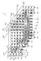
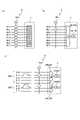
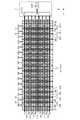
具体的には、本実施形態に係る不揮発性半導体記憶装置1は、図1に示すように構成され得る。図1は、不揮発性半導体記憶装置1の概略構成を示す図である。不揮発性半導体記憶装置1は、通信媒体2を介して、ホスト3と接続可能である。不揮発性半導体記憶装置1は、例えば、抵抗変化型メモリである。通信媒体2は、例えば、同期式並列通信線である。ホスト3は、例えば、コントローラ又はCPUである。不揮発性半導体記憶装置1、通信媒体2、ホスト3を含む構成は、メモリシステム4として構成され得る。メモリシステムは、SDカード等のメモリカードでもよいし、SSD等のストレージシステムでもよいし、eMMCデバイスでもよい。ホスト3は、コントローラでもよいし、CPUでもよい。 Specifically, the nonvolatile
不揮発性半導体記憶装置1は、セルアレイ5、ロウデコーダ6、センスアンプ7、周辺回路8、及びインターフェース部(I/F部)13を有する。周辺回路8は、ドライバ9、シーケンサ10、アドレスレジスタ11、コマンドレジスタ12を含む。セルアレイ5は、複数のメモリセルが配列される。複数のメモリセルは、複数のワード線と複数のビット線とを用いてアクセス可能である。複数のワード線は、それぞれがロウアドレスに対応付けられる。複数のビット線は、それぞれがカラムアドレスに対応付けられる。コマンドレジスタ12は、I/F部13を介してホスト3から受けるホスト要求に含まれるコマンドを保持する。アドレスレジスタ11は、I/F部13を介してホスト3から受けるホスト要求に含まれるアドレスを保持する。 The nonvolatile
シーケンサ10は、コマンドレジスタ12に保持されるコマンドを実行し、セルアレイ5に対するデータのライト動作又はリード動作を制御する。シーケンサ10による制御に応じて、ロウデコーダ6は、アドレスレジスタ11に保持されるアドレスをデコードし、デコードされたロウアドレスに対応するワード線を選択可能である。シーケンサ10による制御に応じて、ドライバ9は、ワード線を選択するための電圧を生成してロウデコーダ6へ供給する。シーケンサ10による制御に応じて、センスアンプ6は、アドレスレジスタ11に保持されるアドレスをデコードし、デコードされたカラムアドレスに対応するビット線を選択可能である。 The
セルアレイ5において複数のメモリセルを3次元的に配列することを考える場合、抵抗変化型メモリ、例えば相変化メモリ(PCM)に適用出来る構成として、鎖接続型メモリがあげられる。鎖接続型メモリでは、複数のメモリセルが鎖状に直列接続されてストリングとして構成される。各メモリセルは、抵抗変化素子とセルトランジスタとの並列接続で構成される。選択メモリセルでセルトランジスタがオフされ、非選択メモリセルでセルトランジスタがオンされることで、選択メモリセルの抵抗変化素子に選択的に電圧を印加可能である。この構造は、3次元のフラッシュメモリに類似した構造で実現出来る。 When considering three-dimensionally arranging a plurality of memory cells in the
例えば、メモリホール内側面にゲート酸化膜、半導体膜、抵抗変化膜、コア絶縁膜を順に堆積して形成可能であるが、その製造時に半導体膜を多結晶半導体で堆積し、その動作時に円筒状の半導体膜に対して軸方向にセル電流が流れることになる。すなわち、鎖接続型メモリでは、ストリングにおける複数のセルトランジスタのチャネル領域が直列接続されることに対応し、抵抗変化素子(抵抗変化膜)へのアクセス動作時に半導体膜を通る電流経路が長くなる。このため、半導体膜における粒界等の影響によりセル電流量が抵抗変化素子のリード・ライトに要求される電流量に対して不足する可能性がある。 For example, it can be formed by sequentially depositing a gate oxide film, a semiconductor film, a variable resistance film, and a core insulating film on the inner side surface of the memory hole. A cell current flows in the axial direction with respect to the semiconductor film. That is, in a chain-connection memory, the channel regions of a plurality of cell transistors in a string are connected in series, and the current path through the semiconductor film becomes longer during the access operation to the variable resistance element (variable resistance film). Therefore, there is a possibility that the amount of cell current will be insufficient for the amount of current required for read/write of the variable resistance element due to the influence of grain boundaries and the like in the semiconductor film.
よって、この対策として、鎖接続型メモリに代えて梯子接続型メモリを採用する。梯子接続型メモリでは、図2に示すような複数のセルブロックCB0~CB11が2次元的に配列されてセルアレイ5が構成される。図2は、セルアレイ5の構成を示す回路図である。セルブロックCBは、複数のメモリセルMCがローカルビット線LBL及びローカルソース線LSL間で梯子状に並列接続されて構成される。各メモリセルMCは、抵抗変化素子REとセルトランジスタMTとの直列接続で構成される。ローカルビット線LBLは、選択トランジスタSGを介してビット線BLに接続される。ローカルソース線LSLは、ソース線SLに接続される。 Therefore, as a countermeasure, a ladder connection type memory is adopted instead of the chain connection type memory. In the ladder connection type memory, a
抵抗変化素子(抵抗変化膜)REへのアクセス動作時には、選択セルブロックCBの選択トランジスタSGをオンし、非選択セルブロックCBの選択トランジスタSGをオフのままにする。選択セルブロックCBでは、選択メモリセルMCのセルトランジスタMTをオンし、非選択メモリセルMCのセルトランジスタMTをオフのままにする。ビット線BLとソース線SLとに電圧を印可すると、ビット線BL→ローカルビット線LBL→選択メモリセルMCの抵抗変化素子RE→選択メモリセルMCのセルトランジスタMT→ローカルソース線LSL→ソース線SLの経路でセル電流が流され得る。 During the access operation to the variable resistance element (variable resistance film) RE, the select transistor SG of the selected cell block CB is turned on, and the select transistor SG of the unselected cell block CB is kept off. In the selected cell block CB, the cell transistors MT of the selected memory cells MC are turned on and the cell transistors MT of the unselected memory cells MC are kept off. When a voltage is applied to the bit line BL and the source line SL, bit line BL → local bit line LBL → resistance change element RE of selected memory cell MC → cell transistor MT of selected memory cell MC → local source line LSL → source line SL. A cell current can flow through the path of
すなわち、梯子接続型メモリでは、セルブロックCBにおける複数のセルトランジスタMTのチャネル領域が並列接続されることに対応し、抵抗変化素子(抵抗変化膜)REへのアクセス動作時に半導体膜を通る電流経路を短くできる。このため、半導体膜内の粒界等の影響で電流が低下しても、セル電流量を抵抗変化素子REのライト動作(Set・Reset動作)及びリード動作(Set・Reset状態の検知)が可能に程度に確保することができる。 That is, in the ladder connection type memory, the channel regions of a plurality of cell transistors MT in the cell block CB are connected in parallel, and the current path through the semiconductor film when the resistance change element (resistance change film) RE is accessed. can be shortened. Therefore, even if the current decreases due to the influence of grain boundaries in the semiconductor film, etc., the amount of cell current can be read (set/reset state detection) and the write operation (set/reset operation) of the variable resistance element RE. can be ensured to a certain extent.
図2に示す回路は、図3に示す構成で実現され得る。図3は、セルアレイ5の構成を示す斜視図である。図3では、ビット線BLの延在方向をY方向とし、メモリセルMCの積層方向をZ方向とし、Y方向及びZ方向に垂直な方向をX方向とする。セルアレイ5は、図3に示すように、基板21の+Z側において、柱状のセルブロックCBがXY方向に2次元的に配列されるとともに、積層体22が柱状のセルブロックCBでZ方向に貫通されて3次元的なメモリセルMCの配列として構成される。 The circuit shown in FIG. 2 can be implemented with the configuration shown in FIG. FIG. 3 is a perspective view showing the configuration of the
基板21の+Z側には、積層体22を含む複数の積層体が配され得る。複数の積層体は、分離部STを間にして互いにY方向にずれた位置に配され得る。分離部STは、少なくとも積層体22に接する面が絶縁物質で形成され、積層体22を他の積層体から電気的に分離している。分離部STは、XZ方向に沿って延びた略フィン形状を有する。 A plurality of laminates including the laminate 22 may be arranged on the +Z side of the
積層体22では、ワード線WLと絶縁層222とが交互に繰り返しZ方向に積層されている。ワード線WLは、XY方向に延びる板状の導電膜で構成される。以下では、ワード線WLを導電膜WLとも呼ぶことにする。積層体22では、複数の導電膜WL0~WL63がZ方向に互いに離間して配置されている。各導電膜WLは、導電物(例えば、タングステンなどの金属)を主成分とする材料で形成され得る。各絶縁層222は、絶縁物(例えば、シリコン酸化物)を主成分とする材料で形成され得る。 In the
積層体22の最上の絶縁層222には、セルブロック選択線SGがZ方向に積層されている。セルブロック選択線SGは、XY方向に延びる板状の導電膜で構成される。以下では、セルブロック選択線SGを導電膜SGとも呼ぶことにする。導電膜SGは、導電物(例えば、タングステンなどの金属)を主成分とする材料で形成され得る。導電膜SGは、分断膜SHEによりY方向に分断される。分断膜SHEは、導電膜WLの上方(+Z側)に設けられ、XZ方向に延在し、積層体22の最上の絶縁層222に達している。分断膜SHEは、絶縁物(例えば、シリコン酸化物)で形成され得る。これにより、各セルブロック選択線SGは、互いに電気的に絶縁される。 Cell block selection lines SG are laminated in the Z direction on the uppermost insulating
各セルブロックCBは、Z方向に延び、積層体22をZ方向に貫通する。セルブロックCBは、複数の導電膜WL0~WL63をZ方向に貫通する柱状構造体で構成される。複数のセルブロックCB0~CB(n-1)は、XY方向に2次元的に配列され得る。各セルブロックCBは、Z方向に延び半導体チャネルとして機能する半導体膜CHを含む。半導体膜CHは、積層体22をZ方向に貫通し、半導体チャネルとして機能する。半導体膜CHと導電膜WLとが交差する位置にはメモリセルMCが構成され、半導体膜CHと導電膜SGとが交差する位置にはセルブロック選択トランジスタSGが構成される。 Each cell block CB extends in the Z direction and penetrates the laminate 22 in the Z direction. The cell block CB is composed of columnar structures penetrating through a plurality of conductive films WL0 to WL63 in the Z direction. A plurality of cell blocks CB0 to CB(n-1) can be arranged two-dimensionally in the XY directions. Each cell block CB includes a semiconductor film CH extending in the Z direction and functioning as a semiconductor channel. The semiconductor film CH penetrates the
導電膜SGの上(+Z側)には、層間絶縁膜23が配されている。層間絶縁膜23は、絶縁物(例えば、シリコン酸化物)を主成分とする材料で形成され得る。 An interlayer insulating
層間絶縁膜23の+Z側には、複数のビット線BL及び複数のソース線SLが配されている。複数のビット線BLは、X方向に配列されている。複数のソース線SLは、それぞれ、複数のビット線BLの間に1つおきに位置するように、X方向に配列されている。ビット線BL及びソース線SLは、それぞれ、Y方向に延びたライン状の導電膜で構成される。ビット線BL及びソース線SLは、それぞれ、導電物(例えば、タングステン、銅、アルミニウムなどの金属)を主成分とする材料で形成され得る。 A plurality of bit lines BL and a plurality of source lines SL are arranged on the +Z side of the
ビット線BLと半導体膜CHとの間には、コンタクトプラグCP1が配されていてもよい。この場合、コンタクトプラグCP1は、上端でビット線BLに接触し、下端で半導体膜CHに接触し、ビット線BL及び半導体膜CHを電気的に接続することができる。コンタクトプラグCP1は、導電物(例えば、タングステンなどの金属)を主成分とする材料で形成され得る。 A contact plug CP1 may be arranged between the bit line BL and the semiconductor film CH. In this case, the contact plug CP1 can be in contact with the bit line BL at its upper end and with the semiconductor film CH at its lower end to electrically connect the bit line BL and the semiconductor film CH. The contact plug CP1 can be made of a material containing a conductor (for example, a metal such as tungsten) as a main component.
ソース線SLとローカルソース線LSLとの間には、コンタクトプラグCP2が配されていてもよい。この場合、コンタクトプラグCP2は、上端でソース線SLに接触し、下端でローカルソース線LSLに接触し、ソース線SL及びローカルソース線LSLを電気的に接続することができる。コンタクトプラグCP2は、導電物(例えば、タングステンなどの金属)を主成分とする材料で形成され得る。 A contact plug CP2 may be arranged between the source line SL and the local source line LSL. In this case, the contact plug CP2 can be in contact with the source line SL at its upper end and with the local source line LSL at its lower end to electrically connect the source line SL and the local source line LSL. The contact plug CP2 can be made of a material containing a conductor (for example, a metal such as tungsten) as a main component.
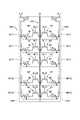
X方向に隣接する2つのセルブロックCBのセットは、1つおきに対を成す。例えば、セルブロックCB0とセルブロックCB3とは対を成し、セルブロックCB3とセルブロックCB6とは対を成さず、セルブロックCB6とセルブロックCB9とは対を成す。 A set of two cell blocks CB adjacent in the X direction forms a pair every other one. For example, cell blocks CB0 and CB3 form a pair, cell blocks CB3 and CB6 do not form a pair, and cell blocks CB6 and CB9 form a pair.
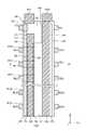
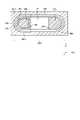
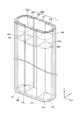
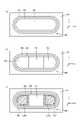
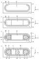
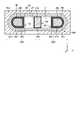
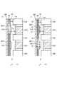
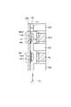
X方向に隣接する2つのセルブロックCBのセットは、例えば、図4~図6に示すように構成される。図4は、セルブロックCBの構成を示す斜視図であり、2つのセルブロックCB0,CB3のセットの構成を例示する。図5は、セルブロックCBの構成を示す垂直方向の断面図であり、セルブロックCBの中心軸を通るXZ断面を示す。図5では、簡略化のため、ワード線WL-ワード線WL間の絶縁層の図示を省略している。図6は、セルブロックCBの構成を示す平面方向の断面図である。図6(a)は、図5をA-A’線で切ったXY断面を示し、図6(b)は、図5をB-B’線で切ったXY断面を示し、図6(c)は、図5をC-C’線で切ったXY断面を示す。 A set of two cell blocks CB adjacent in the X direction is configured as shown in FIGS. 4 to 6, for example. FIG. 4 is a perspective view showing the configuration of the cell block CB, exemplifying the configuration of a set of two cell blocks CB0 and CB3. FIG. 5 is a vertical sectional view showing the configuration of the cell block CB, showing an XZ section passing through the central axis of the cell block CB. In FIG. 5, illustration of an insulating layer between word lines WL is omitted for simplification. FIG. 6 is a cross-sectional view in the plane direction showing the configuration of the cell block CB. FIG. 6(a) shows an XY cross section taken along line AA' in FIG. 5, FIG. 6(b) shows an XY cross section taken along line BB' in FIG. ) shows an XY cross section taken along line CC' of FIG.
セットにおけるセルブロックCB0とセルブロックCB3とは、それぞれ、図4~図6に示すように、柱状構造体で構成される。柱状構造体は、X方向を長手方向とするXY平面形状を有するとともにそのXY断面形状で柱状にZ方向に延びた3次元形状を有する。セルブロックCB0の柱状構造体とセルブロックCB3の柱状構造体とはX方向に結合され、セルブロックCB0とセルブロックCB3とのセットは、略楕円柱形状を有する。 Cell block CB0 and cell block CB3 in the set are each composed of a columnar structure, as shown in FIGS. The columnar structure has an XY planar shape whose longitudinal direction is the X direction, and has a three-dimensional shape extending in the Z direction like a column in its XY cross-sectional shape. The columnar structures of cell block CB0 and the columnar structures of cell block CB3 are coupled in the X direction, and the set of cell blocks CB0 and CB3 has a substantially cylindric shape.
各セルブロックの柱状構造体は、ゲート絶縁膜GD、半導体膜CH、ローカルビット線柱LBL、ローカルソース線柱LSL、抵抗変化膜REを有する。ローカルソース線柱LSLは、セルブロックCB0とセルブロックCB3とのセットで共有されるが、柱状構造体における他の構成は、セルブロックCB0とセルブロックCB3とでそれぞれ設けられる。 The columnar structure of each cell block has a gate insulating film GD, a semiconductor film CH, a local bit line pillar LBL, a local source line pillar LSL, and a resistance change film RE. The local source line pillar LSL is shared by the set of cell block CB0 and cell block CB3, but other configurations in the columnar structure are provided for cell block CB0 and cell block CB3, respectively.
ゲート絶縁膜GDは、Z方向に延びて複数の導電膜WL0~WL63を貫通する。ゲート絶縁膜GDは、略楕円筒形状を有する。半導体膜CHは、ゲート絶縁膜GDの内側でZ方向に延びて複数の導電膜WL0~WL63を貫通する。半導体膜CHは、略楕円筒形状を有し、その外側面がゲート絶縁膜GDの内側面に接している。ローカルビット線柱LBLは、半導体膜CHの内側でZ方向に延びて複数の導電膜WL0~WL63を貫通する。ローカルビット線柱LBLは、略半円柱形状を有する。ローカルソース線柱LSLは、半導体膜CHの内側でZ方向に延びて複数の導電膜WL0~WL63を貫通する。ローカルソース線柱LSLは、略角柱形状を有する。抵抗変化膜REは、半導体膜CHの内側で且つローカルビット線柱LBLの外側で複数の導電膜WL0~WL63を貫通する。抵抗変化膜REは、半導体膜CHに接触する部分とローカルビット線柱LBLに接触する部分とを含む。すなわち、抵抗変化膜REは、略半円筒形状を有し、その外側面が半導体膜CHの内側面に接し、その内側面がローカルビット線柱LBLの外側面に接する。 The gate insulating film GD extends in the Z direction and penetrates the plurality of conductive films WL0 to WL63. The gate insulating film GD has a substantially elliptical cylindrical shape. The semiconductor film CH extends in the Z direction inside the gate insulating film GD and penetrates the plurality of conductive films WL0 to WL63. The semiconductor film CH has a substantially elliptical cylindrical shape, and its outer side surface is in contact with the inner side surface of the gate insulating film GD. The local bit line pillar LBL extends in the Z direction inside the semiconductor film CH and penetrates the plurality of conductive films WL0 to WL63. Local bit line pillar LBL has a substantially semi-cylindrical shape. The local source line pillar LSL extends in the Z direction inside the semiconductor film CH and penetrates the plurality of conductive films WL0 to WL63. The local source line pillar LSL has a substantially prismatic shape. The variable resistance film RE penetrates the plurality of conductive films WL0 to WL63 inside the semiconductor film CH and outside the local bit line pillar LBL. The variable resistance film RE includes a portion in contact with the semiconductor film CH and a portion in contact with the local bit line pillar LBL. That is, the variable resistance film RE has a substantially semi-cylindrical shape, the outer side surface of which is in contact with the inner side surface of the semiconductor film CH, and the inner side surface of which is in contact with the outer side surface of the local bit line pillar LBL.
これらのセルブロックCBは、次のような製造プロセスで製造され得る。半導体基板21(図3参照)の+Z側に絶縁層222と犠牲層SFとを交互に複数回積層し、積層体を形成する。絶縁層222は、例えばシリコン酸化物を主成分とする材料で形成され、犠牲層SFは、例えばシリコン窒化物を主成分とする材料で形成される。セルブロックCBを形成するため、それぞれが積層体をZ方向に貫通する複数のメモリホールMHを形成し、各メモリホールMHに2個のセルブロックCBのセットを埋め込む。その後、犠牲層SFを除去し、それによって形成された空隙に導電膜WLを埋め込む事により、非常に低コストのメモリを実現出来る。 These cell blocks CB can be manufactured by the following manufacturing process. The insulating
2個のセルブロックCBのセットの埋め込みとしては、図4、図5及び図6(a)~図6(c)に示す様に、XY平面視横長のメモリホールMHの側壁外周に、ゲート酸化膜GDが堆積され、その内側に半導体膜CHが堆積され、その後内部を絶縁膜DFで埋めた後、リソグラフィを用いて、図中の中央、左右の3つのサブホールSHを形成する。図中中央のサブホールSHには、内部にタングステン等を用いて低抵抗のローカルソース線柱LSLを埋める。セルブロック選択線SGのZ位置、セルブロック選択線SG及び導電膜WLの間のZ位置では、図6(a)、図6(b)に示すように、半導体膜CHに接しないが、導電膜WLに対応したZ位置では、図6(c)に示すように、半導体膜CHと接する構造にする。図中左右のサブホールSHでは、半導体膜CHの内側に半導体膜CHに接するように抵抗変化膜REを堆積するが、セルブロック選択線SGのZ位置、セルブロック選択線SG及び導電膜WLの間のZ位置では、図6(a)、図6(b)に示すように、抵抗変化膜REを除去する。半導体膜CHに対してもX方向中央付近で且つ導電膜WL直上のZ位置までの部分を除去する。その更に内側にはタングステン等の低抵抗のローカルビット線柱LBLを埋めるが、セルブロック選択線SGのZ位置では、図6(a)に示すように、ローカルビット線柱LBLを除去する。 As shown in FIGS. 4, 5, and 6(a) to 6(c), the embedding of the set of two cell blocks CB is performed by burying a gate oxidation layer around the side wall of the memory hole MH, which is oblong in the XY plan view. A film GD is deposited, a semiconductor film CH is deposited inside it, and then the inside is filled with an insulating film DF. Then, lithography is used to form three sub-holes SH at the center, left and right in the drawing. A sub-hole SH in the center of the figure is filled with a low-resistance local source line pillar LSL using tungsten or the like. At the Z position of the cell block selection line SG and at the Z position between the cell block selection line SG and the conductive film WL, as shown in FIGS. At the Z position corresponding to the film WL, as shown in FIG. 6C, the structure is made in contact with the semiconductor film CH. In the left and right sub-holes SH in the drawing, the resistance change film RE is deposited inside the semiconductor film CH so as to be in contact with the semiconductor film CH. At the Z position in between, as shown in FIGS. 6A and 6B, the variable resistance film RE is removed. The semiconductor film CH is also removed in the vicinity of the center in the X direction and up to the Z position just above the conductive film WL. A local bit line pillar LBL of low resistance such as tungsten is buried further inside, but at the Z position of the cell block selection line SG, the local bit line pillar LBL is removed as shown in FIG. 6(a).
これにより、セルブロック選択線SGのZ位置では、セルブロック選択線SGで制御可能であるセルブロック選択トランジスタSGが形成出来、ビット線BL0,BL1とローカルビット線LBL0,LBL1の接続スイッチが形成出来る。また、セルブロック選択線SG及び導電膜WLの間のZ位置では、ローカルビット線LBLは半導体膜CHに電気的に接続されるので、セルブロック選択トランジスタSGがON状態では、ビット線BL0,BL1に電気的に接続される。また、導電膜WLに対応したZ位置では、ローカルビット線柱LBLが抵抗変化膜RE及び半導体膜CH経由でローカルソース線柱LSLに接続されるので、メモリセルMCが形成され得る。例えば、抵抗変化膜REをカルコゲナイド系の材料(Ge、Sb、Te)等の相変化材料で形成すれば、メモリセルMCをPCMメモリセルとして構成できる。 As a result, at the Z position of the cell block selection line SG, a cell block selection transistor SG that can be controlled by the cell block selection line SG can be formed, and a connection switch between the bit lines BL0, BL1 and the local bit lines LBL0, LBL1 can be formed. . At the Z position between the cell block selection line SG and the conductive film WL, the local bit line LBL is electrically connected to the semiconductor film CH. is electrically connected to Also, at the Z position corresponding to the conductive film WL, the local bit line pillar LBL is connected to the local source line pillar LSL via the resistance change film RE and the semiconductor film CH, so that the memory cell MC can be formed. For example, if the resistance change film RE is made of a phase change material such as a chalcogenide material (Ge, Sb, Te), the memory cell MC can be configured as a PCM memory cell.
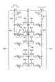
セルブロックCB0とセルブロックCB3とのセットの等価回路図は、図7のようになる。図7は、セルブロックCBの構成を示す回路図である。 An equivalent circuit diagram of a set of cell block CB0 and cell block CB3 is shown in FIG. FIG. 7 is a circuit diagram showing the structure of cell block CB.
図7の等価回路図に示す様に、メモリセルMCは、ワード線WLi(i=0~63)に接続されるセルトランジスタMTと2端子型の抵抗変化素子REとの直列接続で構成される。ワード線WL0~WL63に各々接続される複数のメモリセルMC0~MC63は、並列接続で、一方を共通のローカルビット線(ローカルビット線LBL0,LBL1)、他方を共通のローカルソース線LSLに接続される。ローカルビット線LBLは、セルブロック選択トランジスタSG0,SG1を介してビット線BL0,BL1に接続される。この構成により、セルブロック選択トランジスタSG0,SG3をONさせてセルブロックCB0,CB3を選択し、選択セルブロックCB0,CB3の内の選択ワード線WLにつながるセルトランジスタMTをONする事により、選択メモリセルMCの抵抗変化素子REに選択的に電圧印可、電流印可が可能になり、ランダムリード、ランダムライトが可能になる。更に、ビット線BL、ソース線SL間の電流経路における直列トランジスタ数は僅か、2個に抑えることが出来、トランジスタのON抵抗が高くても十分に抵抗変化素子REのSet/Reset動作が可能な電流を供給できる。 As shown in the equivalent circuit diagram of FIG. 7, the memory cell MC is composed of a serial connection of a cell transistor MT connected to a word line WLi (i=0 to 63) and a two-terminal variable resistance element RE. . A plurality of memory cells MC0 to MC63 respectively connected to word lines WL0 to WL63 are connected in parallel, one of which is connected to a common local bit line (local bit lines LBL0 and LBL1) and the other of which is connected to a common local source line LSL. be. Local bit line LBL is connected to bit lines BL0 and BL1 via cell block select transistors SG0 and SG1. With this configuration, the cell block selection transistors SG0 and SG3 are turned on to select the cell blocks CB0 and CB3, and by turning on the cell transistors MT connected to the selected word line WL in the selected cell blocks CB0 and CB3, the selected memory is selected. It becomes possible to selectively apply voltage and current to the resistance change element RE of the cell MC, and random read and random write become possible. Furthermore, the number of series transistors in the current path between the bit line BL and the source line SL can be reduced to a mere two, and even if the ON resistance of the transistor is high, the set/reset operation of the variable resistance element RE can be sufficiently performed. Can supply current.
この例では、ローカルソース線LSLを共通とした、左右2つのセルブロックCB0,CB3の等価回路を示している。共通のワード線WL1、セルブロック制御線SGを使っており、2つのセルブロックCB0,CB3の2つのセルブロックCB0,CB3のメモリセルMC1を同時にリード/ライトしても良い。 This example shows an equivalent circuit of two left and right cell blocks CB0 and CB3 with a common local source line LSL. A common word line WL1 and cell block control line SG are used, and the memory cells MC1 of the two cell blocks CB0 and CB3 of the two cell blocks CB0 and CB3 may be read/written simultaneously.
あるいは、図8に示す様に、図中右側のセルブロックCB3に対応するビット線BL1の電位をソース線SL電位と均等な固定電位にして、選択ワード線WL1に電圧を印加する。これにより、セルブロックCB3は、選択ワード線WL1に対応したメモリセルMC1に電圧が印可されず、非アクセスとされ得る。図中左側のセルブロックCB0に対応した(ビット線BL0の電位)>(ソース線SLの電位)とする。これにより、セルブロックCB0は、選択ワード線WL1に対応したメモリセルMC1に選択的にセル電流が流れてリード/ライトされ得る。この場合、電流パスとしては、図5、図6(c)及び図8に示すように、選択セルブロックCB0のローカルビット線柱LBLから選択メモリセルMC1の半導体膜CHを介して中央のローカルソース線柱LSLに向かって電流が流れるパスになる。図8は、セルブロックCBの動作を示す回路図であり、選択ワード線がWL1である場合の電流パスを一点鎖線で示している。この時、抵抗変化膜REの抵抗状態(Set,Reset状態)に応じて電流量が変わるため、リード動作が可能になる。積層したワード線WLの開口部に配されるセルトランジスタMTは通常ポリシリコンチャンネルで移動度がバルクトランジスタに比べて非常に低いが、アクセス時のセルブロックCBの直列トランジスタ(図8の場合、セルブロックトランジスタSGと1つのセルトランジスタMT)の数が2個と少ないため、十分大きなセル電流が流され得る。この為、抵抗変化素子REのSet/Reset駆動動作が容易になる。ローカルビット線柱LBLやローカルソース線柱LSLを低抵抗のタングステン等で形成すると、ワード線WLの積層数を増やしても抵抗変化素子REのリード、ライト動作時のセル電流が殆ど減らない為、低コストのメモリが実現出来る。 Alternatively, as shown in FIG. 8, the potential of the bit line BL1 corresponding to the cell block CB3 on the right side of the figure is set to a fixed potential equal to the potential of the source line SL, and a voltage is applied to the selected word line WL1. Accordingly, in the cell block CB3, no voltage is applied to the memory cell MC1 corresponding to the selected word line WL1, and the cell block CB3 can be made non-accessible. It is assumed that (potential of bit line BL0)>(potential of source line SL) corresponding to cell block CB0 on the left side of the drawing. Thereby, the cell block CB0 can be read/written by selectively flowing a cell current to the memory cell MC1 corresponding to the selected word line WL1. In this case, as a current path, as shown in FIGS. 5, 6C, and 8, from the local bit line pillar LBL of the selected cell block CB0 to the central local source through the semiconductor film CH of the selected memory cell MC1. It becomes a path through which current flows toward the line pole LSL. FIG. 8 is a circuit diagram showing the operation of the cell block CB, and shows the current paths when the selected word line is WL1 by dashed lines. At this time, since the amount of current changes according to the resistance state (Set, Reset state) of the resistance change film RE, the read operation becomes possible. The cell transistors MT arranged at the openings of the stacked word lines WL are usually polysilicon channels and have very low mobility compared to bulk transistors. Since the number of block transistors SG and one cell transistor MT is as small as two, a sufficiently large cell current can flow. This facilitates the Set/Reset drive operation of the variable resistance element RE. If the local bit line pillars LBL and local source line pillars LSL are made of low-resistance tungsten or the like, even if the number of stacked word lines WL is increased, the cell current during read and write operations of the variable resistance element RE hardly decreases. A low-cost memory can be realized.
以上のように、第1の実施形態によれば、複数のワード線は、互いに離間して積層された複数の導電膜で構成され、セルブロックは、積層方向に複数の導電膜を貫通する柱状構造体で構成される。この構造は、絶縁層と犠牲層SFとが交互に積層された積層体にメモリホールMHを設けて、その中にセルブロックCBを1個または数個埋め込むことで形成出来、製造コストを大幅に削減できる。更に、複数個のメモリセルの並列接続にブロック選択トランジスタをつないでセルブロックを構成する為、セルブロック内で動作時にセル電流が経由する直列トランジスタ数を2個程度に抑えることが出来る。これにより、セル電流を容易に大きくでき、抵抗変化素子REのSet/Reset駆動動作が容易になる。この為、集積度が高く低コストのメモリが実現出来る。 As described above, according to the first embodiment, a plurality of word lines are composed of a plurality of conductive films stacked with a space therebetween, and a cell block is a columnar cell extending through the plurality of conductive films in the stacking direction. Consists of a structure. This structure can be formed by providing a memory hole MH in a laminated body in which insulating layers and sacrificial layers SF are alternately laminated, and embedding one or several cell blocks CB therein, thereby significantly reducing the manufacturing cost. can be reduced. Furthermore, since a cell block is formed by connecting a block selection transistor to a plurality of memory cells connected in parallel, the number of series transistors through which a cell current passes during operation within the cell block can be suppressed to about two. Thereby, the cell current can be easily increased, and the Set/Reset driving operation of the resistance change element RE becomes easy. Therefore, a memory with a high degree of integration and low cost can be realized.
また、第1の実施形態によれば、ローカルビット線柱LBLやローカルソース線柱LSLを低抵抗のタングステン等で形成する場合、ワード線WLの積層数を増やしてもリード、ライト動作時のセル電流が殆ど減らない。この点からも、集積度が高く低コストのメモリが実現出来る。 Further, according to the first embodiment, when the local bit line pillars LBL and the local source line pillars LSL are made of low-resistance tungsten or the like, even if the number of layers of the word lines WL is increased, the cell during read and write operations remains unchanged. The current hardly decreases. Also from this point, a memory with a high degree of integration and a low cost can be realized.
(第2の実施形態)
次に、第2の実施形態にかかる不揮発性半導体記憶装置1について説明する。以下では、第1の実施形態と異なる部分を中心に説明する。(Second embodiment)
Next, the nonvolatile
第1の実施形態では、2つのセルブロックのセットがメモリホールMH内に配される構成が例示されるが、第2の実施形態では、1つのセルブロックがメモリホールMH内に配される構成が例示される。 The first embodiment exemplifies a configuration in which a set of two cell blocks is arranged in the memory hole MH, but the second embodiment exemplifies a configuration in which one cell block is arranged in the memory hole MH. is exemplified.
セルブロックCBは、例えば、図9~図11に示すように構成される。図9は、セルブロックCBの構成を示す斜視図であり、セルブロックCB0の構成を例示する。図10は、セルブロックCBの構成を示す垂直方向の断面図であり、セルブロックCBの中心軸を通るXZ断面を示す。図10では、簡略化のため、ワード線WL-ワード線WL間の絶縁層の図示を省略している。図11は、セルブロックCBの構成を示す平面方向の断面図である。図11は、図10をD-D’線で切ったXY断面を示す。 The cell block CB is configured as shown in FIGS. 9 to 11, for example. FIG. 9 is a perspective view showing the configuration of the cell block CB, exemplifying the configuration of the cell block CB0. FIG. 10 is a vertical sectional view showing the configuration of the cell block CB, showing an XZ section passing through the central axis of the cell block CB. In FIG. 10, illustration of an insulating layer between word lines WL is omitted for simplification. FIG. 11 is a cross-sectional view in the planar direction showing the configuration of the cell block CB. FIG. 11 shows an XY section of FIG. 10 taken along line D-D'.
セルブロックCB0は、図9~図11に示すように、柱状構造体で構成される。柱状構造体は、X方向を長手方向とするXY平面形状を有するとともにそのXY断面形状で柱状にZ方向に延びた3次元形状を有する。セルブロックCB0は、略楕円柱形状を有する。 The cell block CB0 is composed of columnar structures, as shown in FIGS. The columnar structure has an XY planar shape whose longitudinal direction is the X direction, and has a three-dimensional shape extending in the Z direction like a column in its XY cross-sectional shape. Cell block CB0 has a substantially elliptical cylindrical shape.
この例では、メモリホールMHに1個のセルブロックCBが配される。これらのセルブロックCBは、次の点で第1の実施形態と異なる製造プロセスで製造され得る。複数のメモリホールMHを形成する工程までは同様であるが、各メモリホールMHに1個のセルブロックCBを埋め込む点が異なる。その後、犠牲層SFを除去し、それによって形成された空隙に導電膜WLを埋め込む事により、非常に低コストのメモリを実現出来る点は、第1の実施形態と同様である。 In this example, one cell block CB is arranged in memory hole MH. These cell blocks CB can be manufactured by a manufacturing process different from that of the first embodiment in the following respects. The steps up to the step of forming a plurality of memory holes MH are the same, but the difference is that one cell block CB is embedded in each memory hole MH. After that, by removing the sacrificial layer SF and embedding the conductive film WL in the voids thus formed, a very low-cost memory can be realized, as in the first embodiment.
1個のセルブロックCBの埋め込みとしては、図9、図10及び図11に示す様に、次の点で第1の実施形態と異なる。絶縁膜DFを埋める工程までは同様であるが、その後、リソグラフィを用いて、メモリホールMH内に図中左右の2つのサブホールSHを形成する点で異なる。図中右側のサブホールSHには、内部にタングステン等を用いて低抵抗のローカルソース線柱LSLを埋めて、半導体膜CHと接する構造にする。図中左側のサブホールSHには、半導体膜CHの内側に半導体膜CHに接するようにカルコゲナイド系の材料(Ge、Sb、Te)等で抵抗変化膜REを堆積するが、セルブロック選択線SGのZ位置、セルブロック選択線SG及び導電膜WLの間のZ位置では、抵抗変化膜REを除去する。その更に内側にはタングステン等の低抵抗のローカルビット線柱LBLを埋めるが、セルブロック選択線SGのZ位置では、ローカルビット線柱LBLを除去する。 As shown in FIGS. 9, 10 and 11, the embedding of one cell block CB differs from the first embodiment in the following points. The steps up to the step of filling the insulating film DF are the same, but the difference is that after that, two sub-holes SH are formed on the left and right in the figure in the memory hole MH using lithography. The sub-hole SH on the right side of the figure is filled with a low-resistance local source line pillar LSL using tungsten or the like to form a structure in contact with the semiconductor film CH. In the sub-hole SH on the left side of the figure, a resistance change film RE is deposited inside the semiconductor film CH so as to be in contact with the semiconductor film CH using a chalcogenide material (Ge, Sb, Te) or the like. , and the Z position between the cell block selection line SG and the conductive film WL, the resistance change film RE is removed. A local bit line pillar LBL of low resistance such as tungsten is buried further inside, but the local bit line pillar LBL is removed at the Z position of the cell block selection line SG.
これにより、セルブロック選択線SGのZ位置では、セルブロック選択線SGで制御可能であるセルブロック選択トランジスタSGが形成出来、ビット線BLとローカルビット線LBLの接続スイッチが形成出来る。また、セルブロック選択線SG及び導電膜WLの間のZ位置では、ローカルビット線LBLは、半導体膜CHに電気的に接続されるので、セルブロック選択トランジスタSGのON状態において、ビット線BLに電気的に接続される。また、導電膜WLに対応したZ位置では、ローカルビット線柱LBLが抵抗変化膜RE及び半導体膜CH経由でローカルソース線柱LSLに接続されるので、メモリセルMCが形成され得る。 As a result, at the Z position of the cell block selection line SG, a cell block selection transistor SG that can be controlled by the cell block selection line SG can be formed, and a connection switch between the bit line BL and the local bit line LBL can be formed. At the Z position between the cell block selection line SG and the conductive film WL, the local bit line LBL is electrically connected to the semiconductor film CH. electrically connected. Also, at the Z position corresponding to the conductive film WL, the local bit line pillar LBL is connected to the local source line pillar LSL via the resistance change film RE and the semiconductor film CH, so that the memory cell MC can be formed.
セルブロックCBの等価回路図は、図12のようになる。図12は、セルブロックの構成を示す回路図である。 An equivalent circuit diagram of the cell block CB is shown in FIG. FIG. 12 is a circuit diagram showing the structure of a cell block.
図12の等価回路図に示す様に、メモリセルMCは、ワード線WLi(i=0~63)に接続されるセルトランジスタMTと、2端子型の抵抗変化素子REとの直列接続で構成される。ワード線WL0~WL63に各々接続される複数のメモリセルMC0~MC63は、並列接続で、一方を共通のローカルビット線LBL、他方を共通のローカルソース線LSLに接続される。ローカルビット線LBLは、セルブロック選択トランジスタSGを介してビット線BLに接続される。 As shown in the equivalent circuit diagram of FIG. 12, the memory cell MC is composed of a serial connection of a cell transistor MT connected to a word line WLi (i=0 to 63) and a two-terminal variable resistance element RE. be. A plurality of memory cells MC0-MC63 respectively connected to word lines WL0-WL63 are connected in parallel, one of which is connected to a common local bit line LBL and the other of which is connected to a common local source line LSL. Local bit line LBL is connected to bit line BL via cell block select transistor SG.
この構成により、セルブロック選択トランジスタSGをONさせてセルブロックCBを選択し、選択セルブロックCBの内の選択ワード線WLにつながるセルトランジスタMTをONする事により、選択メモリセルMCの抵抗変化素子REに選択的に電圧印可、電流印可が可能になり、ランダムリード、ランダムライトが可能になる。更に、図13に示すように、ビット線BL、ソース線SL間の電流経路における直列トランジスタ数は僅か、2個に抑えることが出来、トランジスタのON抵抗が高くても十分に抵抗変化素子REにSet/Reset動作が可能な電流を供給できる。図13は、セルブロックの動作を示す回路図である。 With this configuration, the cell block selection transistor SG is turned on to select the cell block CB, and by turning on the cell transistor MT connected to the selected word line WL in the selected cell block CB, the resistance change element of the selected memory cell MC is selected. It becomes possible to selectively apply voltage and current to RE, and random read and random write become possible. Furthermore, as shown in FIG. 13, the number of series transistors in the current path between the bit line BL and the source line SL can be reduced to a mere two, and even if the ON resistance of the transistor is high, the resistance change element RE can sufficiently operate. A current capable of Set/Reset operation can be supplied. FIG. 13 is a circuit diagram showing the operation of the cell block.
以上のように、第2の実施形態では、1つのセルブロックCBがメモリホールMH内に配される柱状構造体で構成される。この構造によっても、複数個のメモリセルMCの並列接続にブロック選択トランジスタSGをつないでセルブロックCBを構成する為、セルブロックCB内で動作時にセル電流が経由する直列トランジスタ数を2個程度に抑えることが出来る。これにより、セル電流を容易に大きくすることができ、抵抗変化素子REのSet/Reset駆動動作が容易になる。この為、集積度が高く低コストのメモリが実現出来る。 As described above, in the second embodiment, one cell block CB is composed of columnar structures arranged in memory holes MH. Also with this structure, since the block selection transistor SG is connected to the parallel connection of a plurality of memory cells MC to configure the cell block CB, the number of series transistors through which the cell current passes during operation within the cell block CB is reduced to about two. can be suppressed. Thereby, the cell current can be easily increased, and the Set/Reset drive operation of the resistance change element RE becomes easy. Therefore, a memory with a high degree of integration and low cost can be realized.
(第3の実施形態)
次に、第3の実施形態にかかる不揮発性半導体記憶装置1について説明する。以下では、第1の実施形態及び第2の実施形態と異なる部分を中心に説明する。(Third Embodiment)
Next, the nonvolatile
第2の実施形態では、1つのメモリセルが1つの抵抗変化素子を含む構成が例示されるが、第3の実施形態では、1つのメモリセルが複数の抵抗変化素子を含む構成が例示される。 The second embodiment exemplifies a configuration in which one memory cell includes one variable resistance element, while the third embodiment exemplifies a configuration in which one memory cell includes a plurality of variable resistance elements. .
セルブロックCBは、例えば、図14~図16に示すように構成される。図14は、セルブロックCBの構成を示す斜視図であり、セルブロックCB0の構成を例示する。図15は、セルブロックCBの構成を示す垂直方向の断面図であり、セルブロックCBの中心軸を通るXZ断面を示す。図15では、簡略化のため、ワード線WL-ワード線WL間の絶縁層の図示を省略している。図16は、セルブロックCBの構成を示す平面方向の断面図である。図16は、図15をE-E’線で切ったXY断面を示す。 The cell block CB is configured as shown in FIGS. 14 to 16, for example. FIG. 14 is a perspective view showing the configuration of the cell block CB, exemplifying the configuration of the cell block CB0. FIG. 15 is a vertical sectional view showing the configuration of the cell block CB, showing an XZ section passing through the central axis of the cell block CB. In FIG. 15, illustration of an insulating layer between word lines WL is omitted for simplification. FIG. 16 is a sectional view in the plane direction showing the structure of the cell block CB. FIG. 16 shows an XY cross section of FIG. 15 taken along line E-E'.
セルブロックCB0は、図14~図16に示すように、柱状構造体で構成される点は第2の実施形態と同様であるが、ローカルソース線柱LSLの側面にも抵抗変化膜RE’が配され、この抵抗変化膜RE’が半導体膜CHと接する構造である点で第2の実施形態と異なる。 As shown in FIGS. 14 to 16, the cell block CB0 is similar to the second embodiment in that it is composed of columnar structures. The second embodiment is different from the second embodiment in that the variable resistance film RE' is in contact with the semiconductor film CH.
これらのセルブロックCBは、次の点で第2の実施形態と異なる製造プロセスで製造され得る。複数のメモリホールMHを形成する工程までは同様であるが、各メモリホールMHに1個のセルブロックCBを埋め込む具体的な工程が異なる。その後、犠牲層SFを除去し、それによって形成された空隙に導電膜WLを埋め込む事により、非常に低コストのメモリを実現出来る点は、第2の実施形態と同様である。 These cell blocks CB can be manufactured by a manufacturing process different from that of the second embodiment in the following respects. The steps up to forming a plurality of memory holes MH are the same, but the specific steps of embedding one cell block CB in each memory hole MH are different. After that, by removing the sacrificial layer SF and embedding the conductive film WL in the voids thus formed, a very low-cost memory can be realized, as in the second embodiment.
1個のセルブロックCBの埋め込みとしては、図14、図15及び図16に示す様に、次の点で第2の実施形態と異なる。図中左右の2つのサブホールSHを形成する工程までは同様であるが、図中右側のサブホールSHと図中左側のサブホールSHとのそれぞれにおいて、半導体膜CHの内側に半導体膜CHに接するようにカルコゲナイド系の材料(Ge、Sb、Te)等で抵抗変化膜RE,RE’を堆積し、セルブロック選択線SGのZ位置、セルブロック選択線SG及び導電膜WLの間のZ位置まで抵抗変化膜RE,RE’を除去する点で異なる。さらに、図中右側のサブホールSHには、抵抗変化膜RE’の内側にはタングステン等の低抵抗のローカルビット線柱LBLを埋めるが、セルブロック選択線SGのZ位置では、ローカルビット線柱LBLを除去する。図中左側のサブホールSHには、抵抗変化膜REの内側にはタングステン等の低抵抗のローカルソース線柱LSLを埋めるが、セルブロック選択線SGのZ位置では、ローカルソース線柱LSLを除去する。 As shown in FIGS. 14, 15 and 16, the embedding of one cell block CB differs from the second embodiment in the following points. The steps up to the step of forming two sub-holes SH on the left and right sides of the drawing are the same, but in each of the sub-hole SH on the right side of the drawing and the sub-hole SH on the left side of the drawing, the semiconductor film CH is formed inside the semiconductor film CH. The resistance change films RE and RE' are deposited from a chalcogenide material (Ge, Sb, Te) or the like so as to be in contact with each other, and the Z position of the cell block selection line SG and the Z position between the cell block selection line SG and the conductive film WL are determined. The difference is that the resistance change films RE and RE' are removed up to. Furthermore, in the sub-hole SH on the right side of the figure, a local bit line pillar LBL of low resistance such as tungsten is embedded inside the resistance change film RE', but the local bit line pillar LBL is buried at the Z position of the cell block selection line SG. Remove the LBL. In the sub-hole SH on the left side of the figure, a local source line pillar LSL of low resistance such as tungsten is embedded inside the variable resistance film RE, but the local source line pillar LSL is removed at the Z position of the cell block selection line SG. do.
これにより、セルブロック選択線SGのZ位置では、ビット線BLとローカルビット線LBLの接続スイッチとしてのセルブロック選択トランジスタSGと、ソース線SLとローカルソース線LSLの接続スイッチとしてのセルブロック選択トランジスタSG’とが形成出来る。また、導電膜WLに対応したZ位置では、ローカルビット線柱LBLが抵抗変化膜RE、半導体膜CH及び抵抗変化膜RE’経由でローカルソース線柱LSLに接続されるので、メモリセルMCが形成され得る。 As a result, at the Z position of the cell block selection line SG, the cell block selection transistor SG as a connection switch between the bit line BL and the local bit line LBL and the cell block selection transistor as a connection switch between the source line SL and the local source line LSL are arranged. SG' can be formed. Also, at the Z position corresponding to the conductive film WL, the local bit line pillar LBL is connected to the local source line pillar LSL via the resistance change film RE, the semiconductor film CH, and the resistance change film RE', so that the memory cell MC is formed. can be
セルブロックCBの等価回路図は、図17のようになる。図17は、セルブロックCBの構成を示す回路図である。 An equivalent circuit diagram of the cell block CB is shown in FIG. FIG. 17 is a circuit diagram showing a structure of cell block CB.
図17の等価回路図に示す様に、メモリセルMCは、2個の抵抗変化素子RE,RE’の間にセルトランジスタMTを挟む構成になる。この構成により、ローカルソース線柱LSLとローカルビット線柱LBLのためのサブホールSHの形成、抵抗変化膜RE,RE’の成膜、ローカルソース線柱LSL及びローカルビット線柱LBLの埋め込みの工程を一回で行え、その製造工程数を削減でき、製造コストを低減できる。 As shown in the equivalent circuit diagram of FIG. 17, the memory cell MC has a configuration in which the cell transistor MT is sandwiched between two variable resistance elements RE and RE'. With this configuration, the steps of forming sub-holes SH for the local source line pillars LSL and local bit line pillars LBL, forming the resistance change films RE and RE', and embedding the local source line pillars LSL and the local bit line pillars LBL. can be performed at one time, the number of manufacturing processes can be reduced, and the manufacturing cost can be reduced.
ただし、図17に示すメモリセルMCでは、2個の抵抗変化膜RE,RE’を同時スイッチする為、図18に示すように、Set時に2個分の電圧印可が行われる。このため、メモリセルMCにおけるトータルのSet電圧が上がる可能性があるが、抵抗変化膜RE,RE’に相変化材料又は超格子材料を用いる場合、各抵抗変化膜のSet電圧を0.8V~1.5V程度にできるので影響は小さい。また、Reset電流は直列であるため、同じ電流を流すだけなので、実質的に影響が無い。更に、抵抗変化素子RE,RE’が高抵抗から低抵抗に変化しやすい場合、どちらか一方が低抵抗化しても、もう一方が高抵抗状態を保持出来ればデータ保持特性の信頼性を大幅に向上できる。図18は、セルブロックCBの動作を示す回路図である。 However, in the memory cell MC shown in FIG. 17, since the two resistance change films RE and RE' are switched simultaneously, two voltages are applied at the time of Set as shown in FIG. For this reason, the total Set voltage in the memory cell MC may increase. Since it can be set to about 1.5V, the influence is small. Also, since the Reset current is in series, the same current only flows, so there is practically no effect. Furthermore, in the case where the resistance change elements RE and RE' easily change from high resistance to low resistance, even if one of them becomes low resistance, if the other can maintain the high resistance state, the reliability of the data retention characteristics can be greatly improved. can improve. FIG. 18 is a circuit diagram showing the operation of cell block CB.
以上のように、第3の実施形態では、1つのセルブロックCBがメモリホールMH内に配される柱状構造体で構成される。セルブロックCBにおける各メモリセルが複数の抵抗変化素子を含むように構成される。これにより、その製造工程数を削減でき、製造コストを低減できるため、さらに低コストのメモリが実現出来る。 As described above, in the third embodiment, one cell block CB is composed of columnar structures arranged in memory holes MH. Each memory cell in cell block CB is configured to include a plurality of variable resistance elements. As a result, the number of manufacturing processes can be reduced, and the manufacturing cost can be reduced, so that a memory with lower cost can be realized.
(第4の実施形態)
次に、第4の実施形態にかかる不揮発性半導体記憶装置1について説明する。以下では、第1の実施形態~第3の実施形態と異なる部分を中心に説明する。(Fourth embodiment)
Next, the nonvolatile
第3の実施形態では、1つのセルブロックCBがメモリホールMH内に配されるセルアレイの構成が例示されるが、第4の実施形態では、1つのセルブロックCBがメモリホールMH内に形成されるセルアレイの製造方法が例示される。 The third embodiment exemplifies the configuration of the cell array in which one cell block CB is arranged in the memory hole MH. In the fourth embodiment, one cell block CB is formed in the memory hole MH. A method of manufacturing a cell array is exemplified.
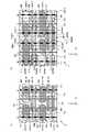
図14~図16に示すセルブロックCBを含むセルアレイ5は、図19(a)~図19(c)に示すように製造される。図19(a)~図19(c)は、それぞれ、セルアレイ5の製造方法を示すXY断面図であり、図15のE-E’線に対応する犠牲膜SFのZ位置で切ったXY断面を示す。 A
半導体基板21(図3参照)の+Z側に絶縁層222と犠牲層SFとを交互に複数回積層し、積層体を形成する。絶縁層222は、例えばシリコン酸化物を主成分とする材料で形成され、犠牲層SFは、例えばシリコン窒化物を主成分とする材料で形成される。セルブロックCBを形成するため、それぞれが積層体をZ方向に貫通する複数のメモリホールMHを形成する。各メモリホールMHは、XY断面視でX方向を長手方向とする略楕円形状で形成され得る。図19(a)に示すように、各メモリホールMHの側壁外周に、ゲート酸化膜GDが堆積され、その内側に半導体膜CHが堆積され、その後内部を絶縁膜DFで埋めた後、絶縁膜DFにおける図中中央部を残しながら図中左右の部分を除去する。リソグラフィを用いて絶縁膜DFにおける図中左右の部分を選択的に露出するレジストパターンでマスキングすることで、絶縁膜DFにおける図中中央部を残しながら図中左右の部分を除去するエッチング加工を行う。図19(b)に示すように、2つのサブホールSHを形成する。その後、図19(c)に示すように、図中右側のサブホールSHと図中左側のサブホールSHとのそれぞれにおいて、半導体膜CHの内側に半導体膜CHに接するようにカルコゲナイド系の材料(Ge、Sb、Te)等の相変化材料で抵抗変化膜RE,RE’を堆積し、セルブロック選択線SGのZ位置、セルブロック選択線SG及び導電膜WLの間のZ位置まで抵抗変化膜RE,RE’を除去する。半導体膜CHに対してもX方向中央付近で且つ導電膜WL直上のZ位置までの部分を除去する。さらに、図中右側のサブホールSHには、抵抗変化膜RE’の内側にはタングステン等の低抵抗のローカルビット線柱LBLを埋めるが、セルブロック選択線SGのZ位置では、ローカルビット線柱LBLを除去し、絶縁膜DFを埋め込む。図中左側のサブホールSHには、抵抗変化膜REの内側にはタングステン等の低抵抗のローカルソース線柱LSLを埋めるが、セルブロック選択線SGのZ位置では、ローカルソース線柱LSLを除去し、絶縁膜DFを埋め込む。その後、犠牲層SFを除去し、それによって形成された空隙に導電膜WLを埋め込む事で、図14~図16に示すセルブロックCBを含むセルアレイ5が製造される。 The insulating
以上のように、第4の実施形態では、1つのセルブロックCBがメモリホールMH内に形成される製造方法において、抵抗変化膜RE,RE’の堆積が同時に行われ得る。ローカルビット線柱LBLの埋め込みとローカルソース線柱LSLの埋め込みとが同時に行われ得る。これにより、製造工程数を少なく抑えて製造コストを低減できるため、低コストのメモリが実現出来る。 As described above, in the fourth embodiment, the resistive films RE and RE' can be deposited simultaneously in the manufacturing method in which one cell block CB is formed in the memory hole MH. The implanting of the local bit line pillars LBL and the local source line pillars LSL can be performed simultaneously. As a result, the number of manufacturing processes can be reduced and the manufacturing cost can be reduced, so that a low-cost memory can be realized.
(第5の実施形態)
次に、第5の実施形態にかかる不揮発性半導体記憶装置1について説明する。以下では、第1の実施形態~第4の実施形態と異なる部分を中心に説明する。(Fifth embodiment)
Next, the nonvolatile
第1の実施形態では、2つのセルブロックCBがメモリホールMH内に配されるセルアレイの構成が例示されるが、第5の実施形態では、2つのセルブロックCBがメモリホールMH内に形成されるセルアレイの製造方法が例示される。 The first embodiment exemplifies the configuration of the cell array in which two cell blocks CB are arranged in the memory holes MH. In the fifth embodiment, two cell blocks CB are formed in the memory holes MH. A method of manufacturing a cell array is exemplified.
図4~図6に示すセルブロックCBを含むセルアレイ5は、図20(a)~図20(d)に示すように製造される。図20(a)~図20(d)は、それぞれ、セルアレイ5の製造方法を示すXY断面図であり、図5のC-C’線に対応する犠牲膜SFのZ位置で切ったXY断面を示す。 A
半導体基板21(図3参照)の+Z側に絶縁層222と犠牲層SFとを交互に複数回積層し、積層体を形成する。絶縁層222は、例えばシリコン酸化物を主成分とする材料で形成され、犠牲層SFは、例えばシリコン窒化物を主成分とする材料で形成される。セルブロックCBを形成するため、それぞれが積層体をZ方向に貫通する複数のメモリホールMHを形成する。各メモリホールMHは、XY断面視でX方向を長手方向とする略楕円形状で形成され得る。図20(a)に示すように、各メモリホールMHの側壁外周に、ゲート酸化膜GDが堆積され、その内側に半導体膜CHが堆積され、その後内部を絶縁膜DFで埋めた後、絶縁膜DFにおける図中中央部を残しながら図中左右の部分を除去する。リソグラフィを用いて絶縁膜DFにおける図中中央部を選択的にレジストパターンでマスキングすることで、絶縁膜DFにおける図中中央部を残しながら図中左右の部分を除去するエッチング加工を行う。図20(b)に示すように、図中の左右の2つのサブホールSHを形成する。図20(c)に示すように、図中左右のサブホールSHでは、半導体膜CHの内側に半導体膜CHに接するように抵抗変化膜REを堆積するが、セルブロック選択線SGのZ位置、セルブロック選択線SG及び導電膜WLの間のZ位置では、抵抗変化膜REを除去する(図6(a)、図6(b)参照)。半導体膜CHに対してもX方向中央付近で且つ導電膜WL直上のZ位置までの部分を除去する。その更に内側にはローカルビット線柱LBLを埋めるが、セルブロック選択線SGのZ位置では、ローカルビット線柱LBLを除去し、絶縁膜DFを埋め込む(図6(a)参照)。図20(d)に示すように、絶縁膜DFにおける図中左右の部分を残しながら図中中央部を除去する。リソグラフィを用いて絶縁膜DFにおける図中中央部を選択的に露出するレジストパターンでマスキングすることで、絶縁膜DFにおける図中左右の部分を残しながら図中中央部を除去するエッチング加工を行う。これにより、図中中央のサブホールSHを形成する。図中中央のサブホールSHには、内部にローカルソース線柱LSLを埋める。セルブロック選択線SGのZ位置、セルブロック選択線SG及び導電膜WLの間のZ位置では、半導体膜CHに接しない(図6(a)、図6(b)参照)が、導電膜WLに対応したZ位置では、半導体膜CHと接する構造(図6(c)参照)にする。その後、犠牲層SFを除去し、それによって形成された空隙に導電膜WLを埋め込む事で、図4~図6に示すセルブロックCBを含むセルアレイ5が製造される。 The insulating
以上のように、第5の実施形態では、2つのセルブロックCBがメモリホールMH内に形成される製造方法において、2つのセルブロックCBの抵抗変化膜REの堆積が同時に行われ得る。2つのセルブロックCBのローカルビット線柱LBLの埋め込みが同時に行われ得る。これにより、製造工程数を削減でき、製造コストを低減できるため、低コストのメモリが実現出来る。 As described above, in the fifth embodiment, in the manufacturing method in which two cell blocks CB are formed in the memory hole MH, deposition of the resistance change films RE of the two cell blocks CB can be performed simultaneously. The implantation of the local bit line pillars LBL of two cell blocks CB can be done at the same time. As a result, the number of manufacturing processes can be reduced, and the manufacturing cost can be reduced, so that a low-cost memory can be realized.
なお、2回のリソグラフィの合わせズレがあると、ローカルソース線柱LSLとローカルビット線柱LBLの距離が変わり(半導体チャネル長が変わり)セルブロックCBの動作特性がばらつく可能性がある。そのことを考慮し、セルアレイ5は、図20(b)~図20(d)に示す工程に代えて、図21(a)~図21(c)に示す工程が行われてもよい。この場合、図20(a)に示す絶縁膜DFにおける図中中央部及び左右の間の部分をマスキングするレジストパターンを用いてエッチング加工を行うことで、図21(a)に示すように、図中中央及び左右の3つのサブホールSHを形成する。図21(b)に点線で示すように、図中中央のサブホールSHを選択的に覆うレジストパターンでマスキングして、図中左右のサブホールSH内に、抵抗変化膜REを堆積し、セルブロック選択線SGのZ位置、セルブロック選択線SG及び導電膜WLの間のZ位置では、抵抗変化膜REを除去する(図6(a)、図6(b)参照)。その後、図21(c)に示すように、マスキングを除去して、図中左右のサブホールSHでは、その更に内側にローカルビット線柱LBLを埋め、図中中央のサブホールSHでは、ローカルソース線柱LSLを埋める。セルブロック選択線SGのZ位置では、ローカルビット線柱LBLを除去し、絶縁膜DFを埋め込む(図6(a)参照)。図中左右のサブホールSHでは、セルブロック選択線SGのZ位置でローカルビット線柱LBLを除去する。 If there is misalignment in lithography twice, the distance between the local source line pillar LSL and the local bit line pillar LBL will change (the semiconductor channel length will change), and there is a possibility that the operating characteristics of the cell block CB will vary. Taking this into consideration, the
このように、図中中央及び左右の3つのサブホールSHを同時に形成でき、ローカルソース線柱LSLとローカルビット線柱LBLの距離が所望の距離になるように容易に形成できる。これにより、セルブロックCBの動作特性のばらつきを抑制できる。 In this manner, the three sub-holes SH at the center and left and right in the drawing can be formed simultaneously, and the distance between the local source line pillar LSL and the local bit line pillar LBL can be easily formed to a desired distance. As a result, variations in operating characteristics of the cell block CB can be suppressed.
(第6の実施形態)
次に、第6の実施形態にかかる不揮発性半導体記憶装置1について説明する。以下では、第1の実施形態~第5の実施形態と異なる部分を中心に説明する。(Sixth embodiment)
Next, the nonvolatile
第1の実施形態では、不揮発性半導体記憶装置1の構成を例示しているが、第6の実施形態では、不揮発性半導体記憶装置1のその構成での動作を例示する。 Although the configuration of the nonvolatile
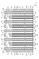
具体的には、不揮発性半導体記憶装置1は、図22に示すように動作し得る。図22は、ストリングブロックの動作例を示す。 Specifically, nonvolatile
図22では、タイミングt1より前において、待機時の動作が行われる。ロウデコーダ6は、ソース線SLをローレベルVL1(例えば、VL1=0V)に維持し、セルブロック選択線SGをローレベルVL2(例えば、VL2=0V又はマイナス電位)に維持し、非選択ワード線WL及び選択ワード線WLをいずれもローレベルVL3(例えば、VL3=0V)に維持する。ワード線WLのローレベルVL3は、セルトランジスタMTのオフ特性を改善するために、マイナス電位(例えば、-2V)であってもよい。セルブロック選択トランジスタSGがオフ状態に維持されるので、ビット線BLは0Vか任意の電位で良い。In FIG. 22, the standby operation is performed before timing t1. The
タイミングt1において、リード・ライト動作が開始される。ロウデコーダ6は、選択セルブロック選択線SGの信号をローレベルVL2からハイレベルVH2へ遷移させ、セルブロックCB0を選択する。At timing t1, a read/write operation is started. The
ワード線WL1に対応するメモリセルMC1を選ぶ場合(図8参照)、ワード線WL1の信号をローレベルVL3からハイレベルVH3へ遷移させ、他のワード線WL0,WL2~WLA63の信号をローレベルVL3に維持する。ワード線WLの信号は、ローレベルVL3が非選択電位であり、ハイレベルVH3が選択電位である。When memory cell MC1 corresponding to word line WL1 is selected (see FIG. 8), the signal on word line WL1 is changed from low levelVL3 to high level VH3, and the signals on other word lines WL0, WL2 toWLA63 are changed to low level. Maintain at levelVL3 . As for the signal on the word line WL, the low levelVL3 is the non-selection potential and the high levelVH3 is the selection potential.
これにより、セルブロックCB0におけるセルブロック選択線SG及びワード線WL1に対応したメモリセルMC1がアクセス出来る。すなわち、ビット線BLとソース線SLとが選択メモリセルMC1の抵抗変化素子REを介して導通する。1つのメモリセルMCが選ばれる状態にして、ソース線SLをローレベルVL1固定にしたまま、複数のビット線BL0,BL1のうち選択ビット線BL0をローレベルVL4からハイレベルVH4へ上げ残りのビット線をローレベルVL4固定とすると選択ビット線BLとソース線SLとの間に電流が流れる。ビット線BLの電位は、ハイレベルVH4が選択電位であり、ローレベルVL4が非選択電位である。As a result, the memory cell MC1 corresponding to the cell block selection line SG and the word line WL1 in the cell block CB0 can be accessed. That is, the bit line BL and the source line SL are brought into conduction through the resistance change element RE of the selected memory cell MC1. One memory cell MC is selected, and while the source line SL is fixed at low levelVL1 , the selected bit line BL0 of the plurality of bit lines BL0 and BL1 is raised from low levelVL4 to high levelVH4 . If the remaining bit lines are fixed at low levelVL4 , current flows between the selected bit line BL and the source line SL. As for the potential of the bit line BL, a high levelVH4 is a selection potential and a low levelVL4 is a non-selection potential.
リード時は、タイミングt1において、ロウデコーダ6は、選択ビット線BLをローレベルVL4からハイレベルVH4へ上げた後にフローティングにする。これに応じて、選択メモリセルMCが高抵抗状態(Reset状態)であればビット線BLの電位が下がりがたくハイレベルVH4近傍に維持される。これにより、センスアンプ7がビット線BLの電位がハイレベルVH4であることを検知し、メモリセルMCから“1”が読み出される。メモリセルMCが低抵抗状態(Set状態)であればビット線BLの電位がローレベルVL4へ下がる。これにより、センスアンプ7がビット線BLの電位がローレベルVL4であることを検知し、メモリセルMCから“0”が読み出される。このとき、セルブロックCB0におけるセル電流が経由するトランジスタ数が2つである。At the time of reading, at timing t1, the
ライト時は、タイミングt1において、センスアンプ7は、ライトしたいビット線BLの電位をローレベルVL4からハイレベルVH4へ上げて、選択メモリセルMCに電流を流す。このときも、セルブロックCB0におけるセル電流が経由するトランジスタ数が2つである。At the time of writing, at timing t1, the
タイミングt1より後のタイミングt2において、センスアンプ7は、急峻にビット線BLの電位をハイレベルVH4からローレベルVL4へ下げれば、選択メモリセルMCの抵抗変化素子(相変化素子)REが急冷されアモルファス化(高抵抗化)される。これにより、メモリセルMCが高抵抗状態(Reset状態)になり、メモリセルMCに“1”が書き込まれる。センスアンプ7は、ゆっくりとビット線BLの電位をハイレベルVH4からローレベルVL4へ下げれば、選択メモリセルMCの抵抗変化素子(相変化素子)REが急冷され結晶化(低抵抗化)される。これにより、メモリセルMCが低抵抗状態(Set状態)になり、メモリセルMCに“0”が書き込まれる。At timing t2 after timing t1, the
その後、リード・ライトが完了することに応じて、各信号が遷移前のレベルに戻され得る。例えば、選択ローカルストリング選択線SGの信号は、ハイレベルVH1からローレベルVL1へ戻される。非選択ワード線WLの信号は、ローレベルVL3に維持されたままである。選択ワード線WLの信号は、ハイレベルVH3からローレベルVL3へ戻される。After that, each signal can be returned to the level before the transition according to the completion of the read/write. For example, the signal on the selected local string select line SG is returned from high levelVH1 to low levelVL1 . The signal on the unselected word lines WL remains at the low levelVL3 . The signal on the selected word line WL is returned from high levelVH3 to low levelVL3 .
以上のように、第6の実施形態では、不揮発性半導体記憶装置1において、選択メモリセルMCに対するリード・ライト動作時にセルブロックCB0におけるセル電流が経由するトランジスタ数が2つである。すなわち、リード・ライト動作時に、セル電流が経由する半導体膜の経路長が抑制されるため、セル電流を容易に大きくすることができ、抵抗変化素子REのSet/Reset駆動動作が容易である。 As described above, in the nonvolatile
なお、第1~第6の実施形態では、センスアンプ7内の構成に言及していないが、センスアンプ7は、例えば図23に示すように構成されてもよい。図23は、第6の実施形態の変形例におけるセンスアンプの構成を示す回路図である。図23では、ビット線BLの本数が8本の場合を例示しているが、ビット線BLの本数は、2~7本であってもよいし、9本以上であってもよい。 Although the first to sixth embodiments do not refer to the internal configuration of the
上記した様に、書きたい、読みたいビット線BLに選択電位の電圧を印可すれば良いため、センスアンプ7は、図23(a)に示すように、全部のビット線BL0~BL7を選択するように構成されてもよい。あるいは、図23(b)に示すように、1本のビット線BLを選択するように構成されてもよい。あるいは、図23(c)に示すように、複数にグループ化されたビット線BLからグループごとに選択された複数のビット線BLを選択するように構成されてもよい。 As described above, since it is sufficient to apply the voltage of the selection potential to the bit lines BL to be written or read, the
図23(a)に示すセンスアンプ7は、複数のビット線BL0~BL7に対応する複数のセンスアンプモジュールSA0~SA7を有する。各センスアンプモジュールSA0~SA7は、対応するビット線BLに接続される。 The
例えば、ロウデコーダ6におけるドライバWL1からワード線WL1へ選択電位であるローレベルVL3(図22参照)が供給された際に、センスアンプ7は、各ビット線BL0~BL7を選択電位であるハイレベルVH4にする。これにより、図23(a)に丸印で示すように、ワード線WL1と複数のビット線BL0~BL7とが交差する位置の各メモリセルMCが選択され、複数のビット線BL0~BL7に流れるセル電流が複数のセンスアンプモジュールSA0~SA7で並行して検知される。これにより、センスアンプ7は、高速にセンスアンプ動作を行うことができる。For example, when a low level VL3 (see FIG. 22), which is a selection potential, is supplied from the driver WL1 in the
あるいは、図23(b)に示すセンスアンプ7は、マルチプレクサMX100及びセンスアンプモジュールSA100を有する。マルチプレクサMX100は、複数のビット線BL0~BL7とセンスアンプモジュールSA100との間に接続されている。センスアンプモジュールSA100は、マルチプレクサMX100を介して複数のビット線BL0~BL7で共有される。これにより、セルアレイ5を複数のサブアレイに細分化した場合に、センスアンプ7の回路面積を低減することができる。 Alternatively, the
例えば、図23(b)に示すように、ロウデコーダ6におけるドライバWL1からワード線WL1へ選択電位であるローレベルVL3(図22参照)が供給された際に、センスアンプ7は、1本のビット線BL1を選択電位であるハイレベルVH4にし、他のビット線BL0,BL2~BL7を非選択電位であるローレベルVL4にする。これに応じて、センスアンプ7は、マルチプレクサMX100を制御して、選択電位が供給されたビット線BL1を選択してセンスアンプモジュールSA100に接続する。これにより、図23(b)に丸印で示すように、ワード線WL1と選択ビット線BL1とが交差する位置の各メモリセルMCが選択され、ワード線WL1と非選択ビット線BL0,BL2~BL7とが交差する位置の各メモリセルMCが非選択とされる。選択ビット線BL1に流れるセル電流がマルチプレクサMX100を介してセンスアンプモジュールSA100で検知される。For example, as shown in FIG. 23B, when a low level VL3 (see FIG. 22), which is a selection potential, is supplied from the driver WL1 in the
あるいは、図23(c)に示すセンスアンプ7は、複数のマルチプレクサMX201,MX202及び複数のセンスアンプモジュールSA201、SA202を有する。マルチプレクサMX201は、複数のビット線BL0~BL3とセンスアンプモジュールSA201との間に接続されている。マルチプレクサMX202は、複数のビット線BL4~BL7とセンスアンプモジュールSA202との間に接続されている。すなわち、複数のビット線BL0~BL3は、センスアンプモジュールSA201に対応してグループGR1にグループ化されているとみなすことができ、複数のビット線BL4~BL7は、センスアンプモジュールSA202に対応してグループGR2にグループ化されているとみなすことができる。 Alternatively, the
センスアンプモジュールSA201は、マルチプレクサMX201を介して複数のビット線BL0~BL3で共有される。センスアンプモジュールSA202は、マルチプレクサMX202を介して複数のビット線BL4~BL7で共有される。これにより、セルアレイ5を複数のサブアレイに細分化した場合に、センスアンプ7の回路面積を低減することができる。 Sense amplifier module SA201 is shared by a plurality of bit lines BL0-BL3 via multiplexer MX201. Sense amplifier module SA202 is shared by a plurality of bit lines BL4-BL7 via multiplexer MX202. Thus, when the
例えば、図23(c)に示すように、ロウデコーダ6におけるドライバWL1からワード線WL1へ選択電位であるローレベルVL3(図22参照)が供給された際に、センスアンプ7は、グループGR1において、1本のビット線BL1を選択電位であるハイレベルVH4にし、他のビット線BL0,BL2~BL3を非選択電位であるローレベルVL4にする。これに応じて、センスアンプ7は、マルチプレクサMX201を制御して、選択電位が供給されたビット線BL1を選択してセンスアンプモジュールSA201に接続する。同様に、センスアンプ7は、グループGR2において、1本のビット線BL5を選択電位であるハイレベルVH4にし、他のビット線BL4,BL6~BL7を非選択電位であるローレベルVL4にする。これに応じて、センスアンプ7は、マルチプレクサMX202を制御して、選択電位が供給されたビット線BL5を選択してセンスアンプモジュールSA202に接続する。For example, as shown in FIG. 23(c), when the driver WL1 in the
これにより、図23(c)に丸印で示すように、グループGR1について、ワード線WL1と選択ビット線BL1とが交差する位置の各メモリセルMCが選択され、ワード線WL1と非選択ビット線BL0,BL2~BL3とが交差する位置の各メモリセルMCが非選択とされる。選択ビット線BL1に流れるセル電流がマルチプレクサMX201を介してセンスアンプモジュールSA201で検知される。同様に、グループGR2について、ワード線WL1と選択ビット線BL5とが交差する位置の各メモリセルMCが選択され、ワード線WL1と非選択ビット線BL4,BL6~BL7とが交差する位置の各メモリセルMCが非選択とされる。選択ビット線BL5に流れるセル電流がマルチプレクサMX202を介してセンスアンプモジュールSA202で検知される。 As a result, as indicated by circles in FIG. 23(c), each memory cell MC at the position where the word line WL1 and the selected bit line BL1 intersect is selected for the group GR1, and the word line WL1 and the unselected bit line are selected. Each memory cell MC at the intersection of BL0, BL2 to BL3 is unselected. A cell current flowing through the selected bit line BL1 is detected by the sense amplifier module SA201 via the multiplexer MX201. Similarly, for group GR2, each memory cell MC at the intersection of word line WL1 and selected bit line BL5 is selected, and each memory cell at the intersection of word line WL1 and unselected bit lines BL4, BL6 to BL7 is selected. Cell MC is deselected. A cell current flowing through the selected bit line BL5 is detected by the sense amplifier module SA202 via the multiplexer MX202.
また、不揮発性半導体記憶装置1において、セルアレイ5が細分化された場合、ビット線BL端に接続されるページバッファ(センスアンプ)面積も削減できる。上記した様に、書きたい、読みたいビット線BLだけに電圧を印可すれば良いため、3次元フラッシュメモリの様に全部のビット線BLのリード/ライトを行っても良いし、クロスポイントメモリの様に1本のビット線BLを選んで行っても良いし、任意のビット線BLを選んでリード/ライトしても良い。例えば8本のビット線BLの1本をリード/ライトしてその次に他の1本と徐々にリード/ライトして時分割でリード/ライトすると、リード/ライトを行うページバッファ(センスアンプ)を8本のビット線BLで共有化出来るため、ビット線BL分割数が多くてもページバッファ面積も削減できる効果が生じる。 Further, in the nonvolatile
(第7の実施形態)
次に、第7の実施形態にかかる不揮発性半導体記憶装置1について説明する。以下では、第1の実施形態~第6の実施形態と異なる部分を中心に説明する。(Seventh embodiment)
Next, the nonvolatile
第1の実施形態では、各セルブロックの抵抗変化膜が一体となっている構成が例示されるが、第7の実施形態では、各セルブロックの抵抗変化膜が複数の抵抗変化膜に分割された構成が例示される。 In the first embodiment, the resistance change film of each cell block is integrated, but in the seventh embodiment, the resistance change film of each cell block is divided into a plurality of resistance change films. configuration is exemplified.
例えば、Z方向に隣接したメモリセルMC間に抵抗変化膜が存在する場合、その抵抗変化膜が高抵抗状態であれば問題無い。しかし、Z方向に隣接するワード線WL間のZ距離が近い場合、Z方向に隣接するメモリセルMC間で抵抗変化膜がワード線WLの電界の影響等により低抵抗化する可能性がある。Z方向に隣接するメモリセルMC間で抵抗変化膜に低抵抗状態の部分があると、メモリセルMC間にディスターバンス電流(リーク電流)が流れる可能性がある。選択メモリセルが高抵抗状態(Reset状態)で隣接する非選択メモリセルが低抵抗状態(Set状態)である場合、Z方向に隣接するメモリセルMC間にディスターバンス電流が流れると、トータルのセル電流がSet状態に対応した電流になってしまい、センスアンプ7でSet状態と誤判定してしまう可能性がある。 For example, if a variable resistance film exists between memory cells MC adjacent in the Z direction, there is no problem if the variable resistance film is in a high resistance state. However, when the Z distance between the word lines WL adjacent in the Z direction is short, the resistance change film between the memory cells MC adjacent in the Z direction may become low in resistance due to the influence of the electric field of the word lines WL. If there is a low-resistance portion in the resistance change film between memory cells MC adjacent in the Z direction, disturbance current (leakage current) may flow between memory cells MC. When a selected memory cell is in a high resistance state (Reset state) and an adjacent unselected memory cell is in a low resistance state (Set state), if a disturbance current flows between adjacent memory cells MC in the Z direction, total The cell current may become a current corresponding to the set state, and the
そのことを考慮し、第7の実施形態では、セルブロックCBは、図24~図26に示すように構成され得る。図24は、セルブロックCBの構成を示す斜視図であり、セルブロックCB0,CB3の構成を例示する。図25は、セルブロックCBの構成を示す垂直方向の断面図であり、各セルブロックCB0,CB3の中心軸を通るXZ断面を示す。図25では、簡略化のため、ワード線WL-ワード線WL間の絶縁層の図示を省略している。図26は、セルブロックCBの構成を示す平面方向の断面図である。図26は、図25をF-F’線で切ったXY断面を示す。 Taking this into consideration, in the seventh embodiment, the cell block CB can be configured as shown in FIGS. 24-26. FIG. 24 is a perspective view showing the structure of the cell block CB, exemplifying the structures of the cell blocks CB0 and CB3. FIG. 25 is a vertical sectional view showing the configuration of the cell block CB, showing an XZ section passing through the central axis of each cell block CB0, CB3. In FIG. 25, illustration of an insulating layer between word lines WL is omitted for simplification. FIG. 26 is a cross-sectional view in the planar direction showing the configuration of the cell block CB. FIG. 26 shows an XY cross section taken along line F-F' in FIG.
各セルブロックCBでは、抵抗変化膜が、複数のワード線WL0~WL63に対応して複数の抵抗変化膜RE0~RE63に分割されている構造が望ましい。複数の抵抗変化膜RE0~RE63は、互いにZ方向に離間しながら積層されている。各抵抗変化膜RE0~RE63は、XY平面視において、ローカルソース線柱LSLに向く側が開放された横U字形状を有する。 In each cell block CB, a structure in which the variable resistance film is divided into a plurality of variable resistance films RE0 to RE63 corresponding to a plurality of word lines WL0 to WL63 is desirable. A plurality of resistance change films RE0 to RE63 are stacked while being spaced apart from each other in the Z direction. Each of the variable resistance films RE0 to RE63 has a horizontal U shape with an open side facing the local source line pillar LSL in the XY plan view.
また、半導体膜CHは、抵抗変化膜RE0~RE63と同じZ位置の第1の部分と複数の抵抗変化膜RE0~RE63の間のZ位置の第2の部分とを有し、第2の部分が第1の部分よりローカルソース線柱LSL側に凹んでいる。これにより、複数の抵抗変化膜RE0~RE63がZ方向に確実に分割され得る。 In addition, the semiconductor film CH has a first portion at the same Z position as the resistance change films RE0 to RE63 and a second portion at a Z position between the plurality of resistance change films RE0 to RE63. is recessed from the first portion toward the local source line pillar LSL. Thereby, the plurality of variable resistance films RE0 to RE63 can be reliably divided in the Z direction.
例えば、図24~図26に示す構造は、次の様に製造され得る。半導体基板21(図3参照)の+Z側に絶縁層222と犠牲層SFとを交互に複数回積層し、積層体を形成する。絶縁層222は、例えばシリコン酸化物を主成分とする材料で形成され、犠牲層SFは、例えばシリコン窒化物を主成分とする材料で形成される。セルブロックCBを形成するため、それぞれが積層体をZ方向に貫通する複数のメモリホールMHを形成する。絶縁層222に対して犠牲層SFの選択比を確保できるエッチャントで犠牲層SFをエッチングし、メモリホールMHの内側面を外側に凹ませる。その後、各メモリホールMHの側壁外周に、ゲート酸化膜GDが堆積され、その内側に半導体膜CHが堆積され、その内側に絶縁膜DFが埋め込まれ、左右のサブホールSH(図20(b)参照)が形成される。左右のサブホールSHでは、その内側面が導電膜WLに対応するZ位置で外側に凹んでいる(図25参照)。左右のサブホールSHでは、抵抗変化膜REを厚めに堆積し、異方性エッチングで抵抗変化膜REをスリミングし、導電膜WL間のZ位置で半導体膜CHを露出させる。これにより、Z方向に分割された複数の抵抗変化膜RE0~RE63が形成される。その後、第5の実施形態と同様の工程が行われ、図24~図26に示す構造が製造される。 For example, the structure shown in FIGS. 24-26 can be manufactured as follows. The insulating
以上のように、第7の実施形態では、各セルブロックCBにおいて、複数の抵抗変化膜RE0~RE63が、複数のワード線WL0~WL63に対応してZ方向に分割されている。これにより、各メモリセルMCの抵抗変化素子RE0~RE63がZ方向に電気的に分離され得るので、Z方向に隣接するメモリセルMC間でディスターバンス電流が流れることを抑制でき、メモリセルMCの抵抗変化素子RE0~RE63に対する書き込みバジェット、読み出しバジェットを改善できる。 As described above, in the seventh embodiment, in each cell block CB, the multiple resistance change films RE0 to RE63 are divided in the Z direction corresponding to the multiple word lines WL0 to WL63. As a result, the resistance change elements RE0 to RE63 of each memory cell MC can be electrically isolated in the Z direction, so that disturbance current can be suppressed from flowing between memory cells MC adjacent to each other in the Z direction. , the write budget and read budget for the variable resistance elements RE0 to RE63 can be improved.
(第8の実施形態)
次に、第8の実施形態にかかる不揮発性半導体記憶装置1について説明する。以下では、第1の実施形態~第7の実施形態と異なる部分を中心に説明する。(Eighth embodiment)
Next, the nonvolatile
第1の実施形態では、各セルブロックにおける抵抗変化膜がローカルビット線柱に接する構成が例示されるが、第8の実施形態では、各セルブロックにおける抵抗変化膜とローカルビット線柱及び半導体膜との間に熱バリア膜が介在する構成が例示される。 The first embodiment exemplifies the configuration in which the variable resistance film in each cell block is in contact with the local bit line pillar. A configuration in which a thermal barrier film is interposed between is exemplified.
例えば、選択メモリセルMCの抵抗変化素子REをSet/Reset動作させる際にセル電流により抵抗変化素子REで発生するジュール熱を利用する。抵抗変化膜REがローカルビット線柱LBLに接する構成では、抵抗変化膜REで発生した熱がローカルビット線柱LBL及び半導体膜CHに漏れるので、選択メモリセルMCの抵抗変化素子REをSet/Reset動作が可能な温度まで昇温するために比較的大きなセル電流を流すことになる。 For example, Joule heat generated in the resistance change element RE due to the cell current is utilized when the resistance change element RE of the selected memory cell MC is set/reset operated. In the configuration in which the resistance change film RE is in contact with the local bit line pillar LBL, the heat generated in the resistance change film RE leaks to the local bit line pillar LBL and the semiconductor film CH. In order to raise the temperature to a temperature at which operation is possible, a relatively large cell current will flow.
そのことを考慮し、第8の実施形態では、セルブロックCBは、図27~図28に示すように構成され得る。図27は、セルブロックCBの構成を示す垂直方向の断面図であり、各セルブロックCB0,CB3の中心軸を通るXZ断面を示す。図27では、簡略化のため、ワード線WL-ワード線WL間の絶縁層の図示を省略している。図28は、セルブロックCBの構成を示す平面方向の断面図である。図28は、図27をG-G’線で切ったXY断面を示す。 Taking this into consideration, in the eighth embodiment, the cell block CB can be configured as shown in FIGS. 27-28. FIG. 27 is a vertical sectional view showing the configuration of the cell block CB, showing an XZ section passing through the central axis of each cell block CB0, CB3. In FIG. 27, illustration of an insulating layer between word lines WL is omitted for simplification. FIG. 28 is a cross-sectional view in the plane direction showing the configuration of the cell block CB. FIG. 28 shows an XY section of FIG. 27 taken along line G-G'.
各セルブロックCBでは、抵抗変化膜REとローカルビット線柱LBLとの間に熱バリア膜HB1が介在する。熱バリア膜HB1は、抵抗変化膜REとローカルビット線柱LBLとの間でZ方向に延びて複数の導電膜WL0~WL63を貫通する。熱バリア膜HB1は、略半円筒形状を有し、その外側面が抵抗変化膜REの内側面に接し、その内側面がローカルビット線柱LBLの外側面に接する。 In each cell block CB, a thermal barrier film HB1 is interposed between the resistance change film RE and the local bit line pillar LBL. The thermal barrier film HB1 extends in the Z direction between the resistance change film RE and the local bit line pillar LBL and penetrates the plurality of conductive films WL0 to WL63. The thermal barrier film HB1 has a substantially semi-cylindrical shape, the outer surface of which contacts the inner surface of the resistance change film RE, and the inner surface of which contacts the outer surface of the local bit line pillar LBL.
抵抗変化膜REと半導体膜CHとの間に熱バリア膜HB2が介在する。熱バリア膜HB2は、抵抗変化膜REと半導体膜CHとの間でZ方向に延びて複数の導電膜WL0~WL63を貫通する。熱バリア膜HB2は、略半円筒形状を有し、その外側面が半導体膜CHの内側面に接し、その内側面が抵抗変化膜REの外側面に接する。このとき、抵抗変化膜REは、半導体膜CHに接触する部分とローカルビット線柱LBLに接触する部分とを含む。 A thermal barrier film HB2 is interposed between the resistance change film RE and the semiconductor film CH. The thermal barrier film HB2 extends in the Z direction between the resistance change film RE and the semiconductor film CH and penetrates the plurality of conductive films WL0 to WL63. The heat barrier film HB2 has a substantially semi-cylindrical shape, the outer side surface of which is in contact with the inner side surface of the semiconductor film CH, and the inner side surface of which is in contact with the outer side surface of the resistance change film RE. At this time, the variable resistance film RE includes a portion in contact with the semiconductor film CH and a portion in contact with the local bit line pillar LBL.
なお、さらに、ローカルソース線柱LSLと半導体膜CHとの間に熱バリア膜HB3が介在してもよい。熱バリア膜HB3は、ローカルソース線柱LSLと半導体膜CHとの間でZ方向に延びて複数の導電膜WL0~WL63を貫通する。熱バリア膜HB3は、略角筒形状を有し、その+Y側,-Y側の外側面が半導体膜CHの内側面に接し、その内側面がローカルソース線柱LSLの外側面に接する。 Furthermore, a thermal barrier film HB3 may be interposed between the local source line pillar LSL and the semiconductor film CH. The thermal barrier film HB3 extends in the Z direction between the local source line pillar LSL and the semiconductor film CH and penetrates the plurality of conductive films WL0 to WL63. The thermal barrier film HB3 has a substantially prismatic shape, and its +Y side and -Y side outer surfaces are in contact with the inner surface of the semiconductor film CH, and the inner surface is in contact with the outer surface of the local source line pillar LSL.
各熱バリア膜HB1,HB2,HB3は、熱抵抗の高い導電物質で形成され、例えばTiN、TaN、TiOx,C,CN等の導電物質で形成される。熱バリア膜HB1は、抵抗変化膜REとローカルビット線柱LBLとの間で電流を通しながら抵抗変化膜REからの熱の漏れを抑制できる。熱バリア膜HB2は、抵抗変化膜REと半導体膜CHとの間で電流を通しながら抵抗変化膜REからの熱の漏れを抑制できる。熱バリア膜HB3は、ローカルソース線柱LSLと半導体膜CHとの間で電流を通しながら抵抗変化膜REからの熱の漏れを抑制できる。 Each of the thermal barrier films HB1, HB2, HB3 is made of a conductive material with high thermal resistance, such as TiN, TaN, TiOx, C, CN, or the like. The thermal barrier film HB1 can suppress heat leakage from the resistance change film RE while conducting current between the resistance change film RE and the local bit line pillar LBL. The thermal barrier film HB2 can suppress heat leakage from the resistance change film RE while conducting current between the resistance change film RE and the semiconductor film CH. The thermal barrier film HB3 can suppress heat leakage from the resistance change film RE while conducting current between the local source line pillar LSL and the semiconductor film CH.
例えば、抵抗変化膜REが相変化材料、磁性材料、金属酸化物材料のいずれで形成される場合も、昇温で動作、或いは高温でスイッチングし易くして動作するので、熱抵抗の高い熱バリア膜HB1,HB2で挟むことで、発熱による熱の逃げを抑え、より低電流で昇温させることが出来る。中央のローカルソース線柱LSLの回りにも熱バリア膜HB3を挿入すれば、抵抗変化膜REの熱エネルギーが半導体膜REを介してローカルソース線柱LSLに逃げるのも防ぐことが出来る。それとともに、熱バリア膜HB1,HB2により、抵抗変化膜REと他の膜との電気的な接触抵抗を下げることが可能となる。 For example, regardless of whether the variable resistance film RE is made of a phase change material, a magnetic material, or a metal oxide material, it operates at elevated temperatures or operates at high temperatures with easy switching. By sandwiching between the films HB1 and HB2, heat escape due to heat generation can be suppressed and the temperature can be raised with a lower current. If the heat barrier film HB3 is also inserted around the central local source line pillar LSL, it is possible to prevent the thermal energy of the resistance change film RE from escaping to the local source line pillar LSL via the semiconductor film RE. At the same time, the thermal barrier films HB1 and HB2 can reduce the electrical contact resistance between the resistance change film RE and other films.
また、熱バリア膜HB1,HB2によれば、抵抗変化膜REへ、或いは抵抗変化膜REからの各種原子の拡散防止が可能になり、データの保持信頼性の劣化を抑制できる。 In addition, the thermal barrier films HB1 and HB2 can prevent diffusion of various atoms to or from the resistance change film RE, thereby suppressing deterioration in data retention reliability.
以上のように、第8の実施形態では、各セルブロックCBにおいて、抵抗変化膜REとローカルビット線柱LBLとの間に熱バリア膜HB1が介在し、抵抗変化膜REと半導体膜CHとの間に熱バリア膜HB2が介在する。これにより、選択メモリセルMCの抵抗変化素子REをSet/Reset動作が可能な温度まで昇温するためのセル電流の大きさを低減でき、不揮発性半導体記憶装置1の消費電力を低減できる。 As described above, in the eighth embodiment, in each cell block CB, the thermal barrier film HB1 is interposed between the resistance change film RE and the local bit line pillar LBL, and the resistance change film RE and the semiconductor film CH are separated from each other. A thermal barrier film HB2 is interposed therebetween. As a result, the magnitude of the cell current for raising the temperature of the variable resistance element RE of the selected memory cell MC to the temperature at which the Set/Reset operation is possible can be reduced, and the power consumption of the nonvolatile
なお、熱バリア膜HB1,HB2の材料として界面の電気抵抗が比較的高い材料を挿入して、界面抵抗での発熱を昇温に用いる熱アシスト機能を持たせてもよい。あるいは、熱バリア膜HB1,HB2の材料を抵抗変化膜REに対する熱的な接触抵抗が高い材料にし、熱バリア膜HB1,HB2及び抵抗変化膜REの界面を初期高抵抗の状態にしてもよい。これにより、抵抗変化膜REがメモリセルMC間で分割された構成(図25参照)にしなくても、導電膜WL間の電流パス分離を実現出来る。このように、熱バリア膜HB1,HB2は、多数の用途に適用可能である。 A material having a relatively high electrical resistance at the interface may be inserted as the material of the thermal barrier films HB1 and HB2 to provide a heat assist function using the heat generated by the interface resistance to raise the temperature. Alternatively, the thermal barrier films HB1 and HB2 may be made of a material having a high thermal contact resistance with respect to the resistance change film RE, and the interface between the thermal barrier films HB1 and HB2 and the resistance change film RE may be in an initial high resistance state. As a result, the current path isolation between the conductive films WL can be realized without the configuration in which the variable resistance film RE is divided between the memory cells MC (see FIG. 25). Thus, the thermal barrier films HB1 and HB2 are applicable to many uses.
(第9の実施形態)
次に、第9の実施形態にかかる不揮発性半導体記憶装置1について説明する。以下では、第1の実施形態~第8の実施形態と異なる部分を中心に説明する。(Ninth embodiment)
Next, the nonvolatile
第9の実施形態では、第7の実施形態と第8の実施形態とを組み合わせる。第9の実施形態では、セルブロックCBは、図29~図30に示すように構成され得る。図29は、セルブロックCBの構成を示す垂直方向の断面図であり、各セルブロックCB0,CB3の中心軸を通るXZ断面を示す。図29では、簡略化のため、ワード線WL-ワード線WL間の絶縁層の図示を省略している。図30は、セルブロックCBの構成を示す平面方向の断面図である。図30は、図29をH-H’線で切ったXY断面を示す。 The ninth embodiment combines the seventh and eighth embodiments. In the ninth embodiment, the cell block CB can be configured as shown in FIGS. 29-30. FIG. 29 is a vertical sectional view showing the configuration of the cell block CB, showing an XZ section passing through the central axis of each cell block CB0, CB3. In FIG. 29, illustration of an insulating layer between word lines WL is omitted for simplification. FIG. 30 is a cross-sectional view in the plane direction showing the configuration of the cell block CB. FIG. 30 shows an XY section of FIG. 29 taken along line H-H'.
各セルブロックCBでは、抵抗変化膜が、複数のワード線WL0~WL63に対応して複数の抵抗変化膜RE0~RE63に分割されている。複数の抵抗変化膜RE0~RE63は、互いにZ方向に離間しながら積層されている。各抵抗変化膜RE0~RE63は、XY平面視において、ローカルソース線柱LSLに向く側が開放された横U字形状を有する。これにより、各メモリセルMCの抵抗変化素子RE0~RE63がZ方向に電気的に分離され得るので、Z方向に隣接するメモリセルMC間でディスターバンス電流が流れることを抑制できる。 In each cell block CB, the variable resistance film is divided into a plurality of variable resistance films RE0 to RE63 corresponding to a plurality of word lines WL0 to WL63. A plurality of resistance change films RE0 to RE63 are stacked while being spaced apart from each other in the Z direction. Each of the variable resistance films RE0 to RE63 has a horizontal U shape with an open side facing the local source line pillar LSL in the XY plan view. As a result, the resistance change elements RE0 to RE63 of each memory cell MC can be electrically isolated in the Z direction, thereby suppressing disturbance current from flowing between memory cells MC adjacent in the Z direction.
抵抗変化膜REとローカルビット線柱LBLとの間に熱バリア膜HB1が介在する。熱バリア膜HB1は、抵抗変化膜REとローカルビット線柱LBLとの間でZ方向に延びて複数の導電膜WL0~WL63を貫通する。熱バリア膜HB1は、略半円筒形状を有し、その外側面が抵抗変化膜REの内側面に接し、その内側面がローカルビット線柱LBLの外側面に接する。 A thermal barrier film HB1 is interposed between the resistance change film RE and the local bit line pillar LBL. The thermal barrier film HB1 extends in the Z direction between the resistance change film RE and the local bit line pillar LBL and penetrates the plurality of conductive films WL0 to WL63. The thermal barrier film HB1 has a substantially semi-cylindrical shape, the outer surface of which contacts the inner surface of the resistance change film RE, and the inner surface of which contacts the outer surface of the local bit line pillar LBL.
抵抗変化膜REと半導体膜CHとの間に熱バリア膜HB2が介在する。熱バリア膜HB2は、抵抗変化膜REと半導体膜CHとの間でZ方向に延びて複数の導電膜WL0~WL63を貫通する。熱バリア膜HB2は、略半円筒形状を有し、その外側面が半導体膜CHの内側面に接し、その内側面が抵抗変化膜REの外側面に接する。 A thermal barrier film HB2 is interposed between the resistance change film RE and the semiconductor film CH. The thermal barrier film HB2 extends in the Z direction between the resistance change film RE and the semiconductor film CH and penetrates the plurality of conductive films WL0 to WL63. The heat barrier film HB2 has a substantially semi-cylindrical shape, the outer side surface of which is in contact with the inner side surface of the semiconductor film CH, and the inner side surface of which is in contact with the outer side surface of the resistance change film RE.
なお、さらに、ローカルソース線柱LSLと半導体膜CHとの間に熱バリア膜HB3が介在してもよい。熱バリア膜HB3は、ローカルソース線柱LSLと半導体膜CHとの間でZ方向に延びて複数の導電膜WL0~WL63を貫通する。熱バリア膜HB3は、略角筒形状を有し、その+Y側,-Y側の外側面が半導体膜CHの内側面に接し、その内側面がローカルソース線柱LSLの外側面に接する。 Furthermore, a thermal barrier film HB3 may be interposed between the local source line pillar LSL and the semiconductor film CH. The thermal barrier film HB3 extends in the Z direction between the local source line pillar LSL and the semiconductor film CH and penetrates the plurality of conductive films WL0 to WL63. The thermal barrier film HB3 has a substantially prismatic shape, and its +Y side and -Y side outer surfaces are in contact with the inner surface of the semiconductor film CH, and the inner surface is in contact with the outer surface of the local source line pillar LSL.
各熱バリア膜HB1,HB2,HB3は、熱抵抗の高い導電物質で形成され、例えばTiN、TaN、TiOx,C,CN等の導電物質で形成される。熱バリア膜HB1は、抵抗変化膜REと半導体膜CHとの間で電流を通しながら抵抗変化膜REからの熱の漏れを抑制できる。熱バリア膜HB2は、抵抗変化膜REと半導体膜CHとの間で電流を通しながら抵抗変化膜REからの熱の漏れを抑制できる。熱バリア膜HB3は、ローカルソース線柱LSLと半導体膜CHとの間で電流を通しながら抵抗変化膜REからの熱の漏れを抑制できる。 Each of the thermal barrier films HB1, HB2, HB3 is made of a conductive material with high thermal resistance, such as TiN, TaN, TiOx, C, CN, or the like. The thermal barrier film HB1 can suppress heat leakage from the resistance change film RE while conducting current between the resistance change film RE and the semiconductor film CH. The thermal barrier film HB2 can suppress heat leakage from the resistance change film RE while conducting current between the resistance change film RE and the semiconductor film CH. The thermal barrier film HB3 can suppress heat leakage from the resistance change film RE while conducting current between the local source line pillar LSL and the semiconductor film CH.
以上のように、第9の実施形態では、各セルブロックCBにおいて、複数の抵抗変化膜RE0~RE63が、複数のワード線WL0~WL63に対応してZ方向に分割されている。これにより、各メモリセルMCの抵抗変化素子RE0~RE63がZ方向に電気的に分離され得るので、Z方向に隣接するメモリセルMC間でディスターバンス電流が流れることを抑制できる。また、各セルブロックCBにおいて、抵抗変化膜REとローカルビット線柱LBLとの間に熱バリア膜HB1が介在し、抵抗変化膜REと半導体膜CHとの間に熱バリア膜HB2が介在する。これにより、選択メモリセルMCの抵抗変化素子REをSet/Reset動作が可能な温度まで昇温するためのセル電流の大きさを低減できる。したがって、メモリセルMCの抵抗変化素子RE0~RE63に対する書き込みバジェット、読み出しバジェットを改善でき、不揮発性半導体記憶装置1の消費電力を低減できる。 As described above, in the ninth embodiment, in each cell block CB, the multiple resistance change films RE0 to RE63 are divided in the Z direction corresponding to the multiple word lines WL0 to WL63. As a result, the resistance change elements RE0 to RE63 of each memory cell MC can be electrically isolated in the Z direction, thereby suppressing disturbance current from flowing between memory cells MC adjacent in the Z direction. In each cell block CB, a thermal barrier film HB1 is interposed between the variable resistance film RE and the local bit line pillar LBL, and a thermal barrier film HB2 is interposed between the variable resistance film RE and the semiconductor film CH. As a result, the magnitude of the cell current for raising the temperature of the variable resistance element RE of the selected memory cell MC to the temperature at which the Set/Reset operation can be performed can be reduced. Therefore, the write budget and read budget for the variable resistance elements RE0 to RE63 of the memory cells MC can be improved, and the power consumption of the nonvolatile
(第10の実施形態)
次に、第10の実施形態にかかる不揮発性半導体記憶装置1について説明する。以下では、第1の実施形態~第9の実施形態と異なる部分を中心に説明する。(Tenth embodiment)
Next, the nonvolatile
第1の実施形態~第9の実施形態では、複数のセルブロックCBのレイアウト構成について言及していないが、第10の実施形態は、複数のセルブロックCBのレイアウト構成について例示する。 Although the first to ninth embodiments do not refer to the layout configuration of a plurality of cell blocks CB, the tenth embodiment illustrates the layout configuration of a plurality of cell blocks CB.
不揮発性半導体記憶装置1において、図31(a)に示すように、複数のセルブロックCB100~CB107がXY方向に2次元的に配列されてセルアレイ5が構成されてもよい。図31(a)は、セルアレイ5の構成を示す平面図であり、1つのセルブロックCBがメモリホールMH内に配される柱状構造体で構成される場合(図9~図11参照)の複数のセルブロックCB100~CB107のレイアウト構成を例示する。 In the nonvolatile
図31(a)に示す様に、複数のセルブロックCB100~CB107は、それぞれがX方向に沿っている複数列を形成するように配列される。セルブロックCB102,CB106の配列が1つの列を形成し、セルブロックCB100,CB104の配列が他の1つの列を形成する。複数列は、Y方向に隣接する列間で配列の半ピッチ分、その配置のX位置がずれている。セルブロックCB100のX位置は、セルブロックCB102のX位置に対して、セルブロックCB102,CB106の配列の半ピッチ分ずれている。これにより、リソグラフィ的に、複数のセルブロックCB100~CB107に対する複数のメモリホールMHの開口が容易になる。 As shown in FIG. 31(a), a plurality of cell blocks CB100 to CB107 are arranged to form a plurality of columns along the X direction. The array of cell blocks CB102 and CB106 forms one column, and the array of cell blocks CB100 and CB104 forms another column. The plural rows are arranged such that the X position of the arrangement is shifted by half the pitch of the arrangement between adjacent rows in the Y direction. The X position of cell block CB100 is shifted from the X position of cell block CB102 by half the pitch of the arrangement of cell blocks CB102 and CB106. This facilitates lithographic opening of the plurality of memory holes MH in the plurality of cell blocks CB100 to CB107.
図31(a)の例では、Y方向で1列おきにダミーのメモリホールMHを形成する。ダミーのセルブロックCB102,CB103,CB106,CB107は、セルブロック選択トランジスタが省略される。この為、分断膜SHEでセルブロック選択信号線SGをY方向に分断している。これにより、X方向に1本毎にビット線BLとソース線SLとを交互に配置しても、セルブロックCBのY方向の配置ピッチを小さくできる。分離パターンISOは、製造時に、ローカルソース線柱LSLを埋め込むためのサブホールSHとローカルビット線柱LBLを埋め込むためのサブホールSH(図19(b)参照)とを分離するマスキング用のレジストパターンのレイアウトである。 In the example of FIG. 31A, dummy memory holes MH are formed every other row in the Y direction. Cell block selection transistors are omitted from dummy cell blocks CB102, CB103, CB106, and CB107. Therefore, the dividing film SHE divides the cell block selection signal line SG in the Y direction. As a result, even if the bit lines BL and the source lines SL are alternately arranged in the X direction, the arrangement pitch of the cell blocks CB in the Y direction can be reduced. The isolation pattern ISO is a masking resist pattern that separates the sub-hole SH for embedding the local source line pillar LSL from the sub-hole SH (see FIG. 19B) for embedding the local bit line pillar LBL during manufacturing. layout.
あるいは、不揮発性半導体記憶装置1において、図31(b)に示すように、複数のセルブロックCB200~CB215がXY方向に2次元的に配列されてセルアレイ5が構成されてもよい。図31(b)は、セルアレイ5の構成を示す平面図であり、2つのセルブロックCBのセットがメモリホールMH内に配される柱状構造体で構成される場合(図4~図6参照)の複数のセルブロックCB200~CB215のレイアウト構成を例示する。 Alternatively, in the nonvolatile
図31(b)に示す様に、複数のセルブロックCB200~CB215は、それぞれがX方向に沿っている複数列を形成するように配列される。セルブロックCB200,CB204のセット、セルブロックCB208,CB212のセットの配列が1つの列を形成し、セルブロックCB201,CB205のセット、セルブロックCB209,CB213のセットの配列が他の1つの列を形成する。複数列は、Y方向に隣接する列間で配列の半ピッチ分、その配置のX位置がずれている。セルブロックCB201,CB205の中間のX位置は、セルブロックCB204,CB208の中間のX位置に対して、セルブロックCB200,CB204のセット、セルブロックCB208,CB212のセットの配列の半ピッチ分ずれている。これにより、リソグラフィ的に、複数のセルブロックCB200~CB215に対する複数のメモリホールMHの開口が容易になる。 As shown in FIG. 31(b), a plurality of cell blocks CB200 to CB215 are arranged to form a plurality of columns along the X direction. A set of cell blocks CB200 and CB204 and a set of cell blocks CB208 and CB212 form one column, and a set of cell blocks CB201 and CB205 and a set of cell blocks CB209 and CB213 form another column. do. The plural rows are arranged such that the X position of the arrangement is shifted by half the pitch of the arrangement between adjacent rows in the Y direction. The middle X position of cell blocks CB201 and CB205 is shifted by half the pitch of the arrangement of the set of cell blocks CB200 and CB204 and the set of cell blocks CB208 and CB212 with respect to the middle X position of cell blocks CB204 and CB208. . This facilitates lithographic opening of the plurality of memory holes MH in the plurality of cell blocks CB200 to CB215.
図31(b)の例では、Y方向で1列おきにダミーのメモリホールMHを形成する。ダミーのセルブロックCB200,CB204,CB208,CB212,202,CB207,CB210,CB214は、セルブロック選択トランジスタが省略される。この為、分断膜SHEでセルブロック選択信号線SGをY方向に分断している。これにより、X方向にビット線BL間に1つおきにソース線SLを配置しても、セルブロックCBのY方向の配線ピッチを小さくできる。分離パターンISOは、製造時に、ローカルソース線柱LSLを埋め込むための中央のサブホールSHとローカルビット線柱LBLを埋め込むための左右のサブホールSH(図21(a)参照)とを分離するマスキング用のレジストパターンのレイアウトである。なお、リソグラフィの容易性にもよるが、最初から分断膜SHE下のメモリホールMHの形成を省略してもよい。 In the example of FIG. 31(b), dummy memory holes MH are formed every other row in the Y direction. Cell block selection transistors are omitted from dummy cell blocks CB200, CB204, CB208, CB212, 202, CB207, CB210, and CB214. Therefore, the dividing film SHE divides the cell block selection signal line SG in the Y direction. Thus, even if the source lines SL are arranged alternately between the bit lines BL in the X direction, the wiring pitch of the cell blocks CB in the Y direction can be reduced. The isolation pattern ISO is masking that separates the central sub-hole SH for burying the local source line pillar LSL and the left and right sub-holes SH (see FIG. 21(a)) for burying the local bit line pillar LBL during manufacturing. 1 is a layout of a resist pattern for . Note that the formation of the memory holes MH under the dividing film SHE may be omitted from the beginning, depending on the easiness of lithography.
以上のように、第10の実施形態では、不揮発性半導体記憶装置1のセルアレイ5において、Y方向に隣接する列間で配列の半ピッチ分X位置がずれた複数列を形成するように複数のセルブロックCB100~CB108がXY方向に2次元的に配列される。これにより、複数のメモリホールMHの形成が容易になり、不揮発性半導体記憶装置1を容易に製造できる。 As described above, in the tenth embodiment, in the
(第11の実施形態)
次に、第11の実施形態にかかる不揮発性半導体記憶装置1について説明する。以下では、第1の実施形態~第10の実施形態と異なる部分を中心に説明する。(Eleventh embodiment)
Next, the nonvolatile
第10の実施形態では、複数のセルブロックCBのレイアウト構成について例示するが、第11の実施形態は、複数のセルブロックCBのレイアウト構成に加えてセンスアンプ7との接続構成についてさらに例示する。 The tenth embodiment exemplifies the layout configuration of a plurality of cell blocks CB, while the eleventh embodiment further exemplifies the connection configuration with the
不揮発性半導体記憶装置1において、図32に示すように、複数のセルブロックCB100~CB108がXY方向に2次元的に配列されてセルアレイ5が構成されてもよい。図32は、セルアレイ5の構成を示す平面図であり、2つのセルブロックCBがメモリホールMH内に配される場合(図31(b)参照)のレイアウト構成を分離部ST間に拡張して示す。複数のビット線BL0~BL7とセンスアンプ7との接続構成は、図23(a)~図23(c)に示すような任意の構成を採用可能であるが、図32では、図23(b)に対応する構成を例示する。 In the nonvolatile
複数のビット線BL0~BL7は、それぞれがY方向に延びるとともに、互いにX方向に配列される。複数のビット線BL0~BL7は、一端側でセンスアンプ7に接続される。複数のビット線BL0~BL7は、例えばマルチプレクサMX100に接続される。 The plurality of bit lines BL0 to BL7 each extend in the Y direction and are arranged in the X direction. A plurality of bit lines BL0 to BL7 are connected to a
複数のソース線SL0~SL3は、それぞれがY方向に延びるとともに、ビット線BL間に1つおきに配されるように互いにX方向に配列される。各ソース線SL0~SL3は、ロウデコーダ6に接続される。複数のソース線SL0~SL3は、センスアンプ7に接続されない。 The plurality of source lines SL0 to SL3 each extend in the Y direction and are arranged in the X direction so as to be arranged alternately between the bit lines BL. Each source line SL0-SL3 is connected to a
ソース線SLが配されないビット線BL間には、シールド線SHLが配されてもよい。複数のシールド線SHL0~SHL2は、それぞれがY方向に延びるとともに、ソース線SL間に配され且つビット線BL間に1つおきに配されるように互いにX方向に配列される。各シールド線SHL0~SHL2は、ロウデコーダ6に接続される。複数のシールド線SHL0~SHL2は、センスアンプ7に接続されない。 A shield line SHL may be arranged between the bit lines BL where the source line SL is not arranged. The plurality of shield lines SHL0 to SHL2 extend in the Y direction and are arranged in the X direction so as to be arranged between the source lines SL and alternately between the bit lines BL. Each shield line SHL0-SHL2 is connected to a
なお、各ソース線SL0~SL3は、ロウデコーダ6から固定電位(例えば、Lレベル)が供給されてもよい。各シールド線SHL0~SHL2は、ロウデコーダ6から固定電位(例えば、Lレベル)が供給されてもよい。これにより、ビット線BL間のクロストークを抑制しながらビット線BL間のX距離を低減できる。 A fixed potential (for example, L level) may be supplied from the
図32に示すセルアレイ5において、複数のセルブロック選択線SG0~SG15は、それぞれがX方向に延びるとともに、分断膜SHEを介して互いにY方向に分断されている。各セルブロックCBは、その長手方向をX方向とする。複数のセルブロックCBは、セルブロック選択線SGに収まるように、X方向に配列されている。複数のセルブロック選択線SG0~SG15及び複数の分断膜SHEの-Z側には、複数層のワード線WL0~WL63が互いにZ方向に離間しながら積層されている(図3参照)。各ワード線WLは、分離部ST間で連続した導電膜で構成されている。図32に示すセルアレイ5では、16本のセルブロック選択線SG0~SG15に対して各ワード線WL0~WL63が共通化されている。 In the
不揮発性半導体記憶装置1では、セルブロック選択線SG、選択ワード線WL、選択ビット線BLの組み合わせにより任意の数のメモリセルMCに対してリード/ライト出来るので、ワード線WLを共有化可能なセルブロック選択線SGの数は任意である。但し、共有化するセルブロック選択線SGの数を多くすると消費電力が増えるので、セルブロック選択線SG16本/ワード線WL1本程度の比率で共有化することが望ましい。図32に示す例では、複数のビット線BL0~BL7の内の1本をマルチプレクサMX100で活性化してセンスアンプモジュールSA100につないでリード/ライトする構成を例示している。1本/8本のビット線BLの活性化により、センスアンプ7のレイアウト面積を約1/8に減らせる効果がある。これにより電流駆動の抵抗変化型メモリであってもビット線BLのIRドロップ低減の為にビット線BL長を短くしてもセンスアンプ7のレイアウト面積の増大を抑制できる。 In the non-volatile
以上のように、第11の実施形態では、不揮発性半導体記憶装置1のセルアレイ5において、複数のビット線BL0~BL7の間にはソース線SL又はシールド線SHLが配される。これにより、ビット線BL間のクロストークを抑制しながらビット線BL間のX距離を低減でき、セルアレイ5のレイアウト面積を容易に低減できる。 As described above, in the eleventh embodiment, in the
(第12の実施形態)
次に、第12の実施形態にかかる不揮発性半導体記憶装置1について説明する。以下では、第1の実施形態~第11の実施形態と異なる部分を中心に説明する。(Twelfth embodiment)
Next, the nonvolatile
第1の実施形態、第8の実施形態では、2つのセルブロックのセットがメモリホールMH内に配される構成が例示されるが、第12の実施形態では、4つのセルブロックのセットがメモリホールMH内に配される構成が例示される。 In the first embodiment and the eighth embodiment, a configuration in which two cell block sets are arranged in the memory hole MH is illustrated, but in the twelfth embodiment, four cell block sets are arranged in the memory. A configuration arranged in the hole MH is exemplified.
セルブロックCBは、例えば、図33~図34に示すように構成される。図33は、セルブロックCBの構成を示す垂直方向の断面図であり、セルブロックCBの中心軸を通るXZ断面を示す。図33では、簡略化のため、ワード線WL-ワード線WL間の絶縁層の図示を省略している。図34は、セルブロックCBの構成を示す平面方向の断面図である。図34は、図33をI-I’線で切ったXY断面を示す。 The cell block CB is configured as shown in FIGS. 33 and 34, for example. FIG. 33 is a vertical sectional view showing the configuration of the cell block CB, showing an XZ section passing through the central axis of the cell block CB. In FIG. 33, illustration of an insulating layer between word lines WL is omitted for simplification. FIG. 34 is a cross-sectional view in the plane direction showing the configuration of the cell block CB. FIG. 34 shows an XY section of FIG. 33 taken along the line I-I'.
図33~図34に示す構造は、図4~図6に示す構造に対して、メモリホールMHの中心を通りX方向に沿った溝で分断して絶縁膜DFを埋め込む変更が行われた構造になっている。 The structures shown in FIGS. 33 and 34 are different from the structures shown in FIGS. 4 to 6 in that they are divided by grooves passing through the center of the memory hole MH along the X direction and filled with the insulating film DF. It has become.
セルブロックCB0とセルブロックCB1との間の絶縁膜DFは、各セルブロックCBの-Z側端まで達しており、セルブロックCB0とセルブロックCB1とを電気的に分離している。セルブロックCB0のローカルビット線柱LBLとセルブロックCB1のローカルビット線柱LBLとは絶縁膜DFで電気的に分離されている。セルブロックCB0の抵抗変化膜REとセルブロックCB1の抵抗変化膜REとは絶縁膜DFで電気的に分離されている。 The insulating film DF between the cell blocks CB0 and CB1 reaches the -Z side end of each cell block CB and electrically separates the cell blocks CB0 and CB1. The local bit line pillars LBL of the cell block CB0 and the local bit line pillars LBL of the cell block CB1 are electrically separated by an insulating film DF. The resistance change film RE of the cell block CB0 and the resistance change film RE of the cell block CB1 are electrically separated by an insulating film DF.
セルブロックCB3とセルブロックCB4との間の絶縁膜DFは、各セルブロックCBの-Z側端まで達しており、セルブロックCB3とセルブロックCB4とを電気的に分離している。セルブロックCB3のローカルビット線柱LBLとセルブロックCB4のローカルビット線柱LBLとは絶縁膜DFで電気的に分離されている。セルブロックCB3の抵抗変化膜REとセルブロックCB4の抵抗変化膜REとは絶縁膜DFで電気的に分離されている。 The insulating film DF between the cell blocks CB3 and CB4 reaches the -Z side end of each cell block CB and electrically separates the cell blocks CB3 and CB4. The local bit line pillars LBL of the cell block CB3 and the local bit line pillars LBL of the cell block CB4 are electrically separated by an insulating film DF. The resistance change film RE of the cell block CB3 and the resistance change film RE of the cell block CB4 are electrically separated by an insulating film DF.
-Y側のローカルソース線柱LSLと+Y側のローカルソース線柱LSLとの間の絶縁膜DFは、各柱の-Z側端まで達しており、-Y側のローカルソース線柱LSLと+Y側のローカルソース線柱LSLとは絶縁膜DFで電気的に分離されている。 The insulating film DF between the −Y side local source line pillar LSL and the +Y side local source line pillar LSL reaches the −Z side end of each pillar. It is electrically separated from the local source line pillar LSL on the side by an insulating film DF.
なお、図33~図34に示すように、各セルブロックCBでは、抵抗変化膜REとローカルビット線柱LBLとの間に熱バリア膜HB1が介在してもよく、抵抗変化膜REと半導体膜CHとの間に熱バリア膜HB2が介在してもよい。さらに、ローカルソース線柱LSLと半導体膜CHとの間に熱バリア膜HB3が介在してもよい。 As shown in FIGS. 33 and 34, in each cell block CB, a thermal barrier film HB1 may be interposed between the resistance change film RE and the local bit line pillar LBL. A thermal barrier film HB2 may be interposed between CH. Furthermore, a thermal barrier film HB3 may be interposed between the local source line pillar LSL and the semiconductor film CH.
図33~図34に示す構造は、図35に示すように、次の点で図20(a)~図20(d)に示す製造方法と異なる製造方法で製造され得る。図35は、セルアレイ5の構成を示す平面図であるが、製造方法を示す図として流用する。 The structure shown in FIGS. 33 and 34 can be manufactured by a manufacturing method different from the manufacturing method shown in FIGS. 20(a) to 20(d) in the following respects, as shown in FIG. FIG. 35 is a plan view showing the configuration of the
図20(d)に示す構造が形成された後、図35(a)に示すように、メモリホールMHの外側のY位置を通りX方向に延びた溝パターンTR1を積層体22の最上の絶縁層222のZ位置(図3参照)まで形成する。また、メモリホールMHの中心のY位置を通りX方向にメモリホールMHを横切って延びメモリホールMHの-Z側端(図3参照)に達する溝パターンTR2を形成する。そして、各溝パターンTR1,TR2に絶縁物質(例えば、シリコン酸化物)を埋め込んで分断膜SHEを形成する。その後、犠牲層SFを除去し、それによって形成された空隙に導電膜WLを埋め込む事で、図33~図34に示す4つのセルブロックのセットを含むセルアレイ5が製造される。 After the structure shown in FIG. 20(d) is formed, as shown in FIG. 35(a), the groove pattern TR1 extending in the X direction through the Y position outside the memory hole MH is formed in the uppermost insulation of the laminate 22. It is formed up to the Z position of layer 222 (see FIG. 3). Further, a trench pattern TR2 is formed which extends across the memory hole MH in the X direction through the Y position of the center of the memory hole MH and reaches the -Z side end (see FIG. 3) of the memory hole MH. Then, an insulating material (for example, silicon oxide) is embedded in each of the trench patterns TR1 and TR2 to form a dividing film SHE. After that, the sacrificial layer SF is removed, and the voids thus formed are filled with the conductive film WL, thereby manufacturing the
あるいは、図20(d)に示す構造が形成された後、図35(b)に示すように、メモリホールMH内で中心のY位置を通りX方向に延びメモリホールMHの-Z側端に達する溝パターンTR3を形成する。そして、溝パターンTR3に絶縁物質(例えば、シリコン酸化物)を埋め込んで絶縁膜DFを形成する。その後、犠牲層SFを除去し、それによって形成された空隙に導電膜WLを埋め込む事によっても、図33~図34に示す4つのセルブロックのセットを含むセルアレイ5が製造される。 Alternatively, after the structure shown in FIG. 20D is formed, as shown in FIG. A trench pattern TR3 is formed. Then, an insulating material (for example, silicon oxide) is embedded in the trench pattern TR3 to form an insulating film DF. After that, the sacrificial layer SF is removed, and the voids thus formed are filled with the conductive film WL, thereby manufacturing the
図33~図34に示す構造は、メモリホールMH内に配されるセルブロック数を多く確保できるので、XY方向のメモリセルMCの配置密度を容易に向上でき、単位記憶容量当たりのチップコストを低減できる。 The structures shown in FIGS. 33 and 34 can secure a large number of cell blocks arranged in the memory holes MH, so that the arrangement density of the memory cells MC in the XY directions can be easily improved, and the chip cost per unit storage capacity can be reduced. can be reduced.
また、セルブロック選択線SGのレイアウト構成については、図35(a)に示すように、メモリホールMH内でY方向に隣接する複数のセルブロックCBが異なるセルブロック選択線SGに対応していてもよい。この場合、メモリホールMH内でY方向に隣接する複数のセルブロックCBのローカルビット線柱LBLは、共通のビット線BLに接続され得る。例えば、セルブロックCB0とセルブロックCB1とは、メモリホールMH内でY方向に隣接する。セルブロックCB0は、セルブロック選択線SG0に対応する。セルブロックCB1は、セルブロック選択線SG1に対応する。セルブロックCB0は、セルブロック選択トランジスタSG0がオンした際にローカルビット線柱LBLがコンタクトプラグCP1を介してビット線BL0に接続され得る。セルブロックCB1は、セルブロック選択トランジスタSG1がオンした際にローカルビット線柱LBLがコンタクトプラグCP1を介してビット線BL0に接続され得る。 As for the layout configuration of the cell block selection lines SG, as shown in FIG. 35A, a plurality of cell blocks CB adjacent in the Y direction within the memory holes MH correspond to different cell block selection lines SG. good too. In this case, the local bit line pillars LBL of the plurality of cell blocks CB adjacent in the Y direction within the memory holes MH can be connected to a common bit line BL. For example, cell block CB0 and cell block CB1 are adjacent in the Y direction within memory hole MH. Cell block CB0 corresponds to cell block select line SG0. Cell block CB1 corresponds to cell block select line SG1. In the cell block CB0, the local bit line pillar LBL can be connected to the bit line BL0 via the contact plug CP1 when the cell block select transistor SG0 is turned on. In the cell block CB1, the local bit line pillar LBL can be connected to the bit line BL0 via the contact plug CP1 when the cell block select transistor SG1 is turned on.
セルブロックCB3とセルブロックCB4とは、メモリホールMH内でY方向に隣接する。セルブロックCB3は、セルブロック選択線SG0に対応する。セルブロックCB4は、セルブロック選択線SG1に対応する。セルブロックCB3は、セルブロック選択トランジスタSG0がオンした際にローカルビット線柱LBLがコンタクトプラグCP1を介して共通のビット線BL1に接続され得る。セルブロックCB4は、セルブロック選択トランジスタSGがオンした際にローカルビット線柱LBLがコンタクトプラグCP1を介してビット線BL1に接続され得る。 Cell block CB3 and cell block CB4 are adjacent in the Y direction within memory hole MH. Cell block CB3 corresponds to cell block select line SG0. Cell block CB4 corresponds to cell block select line SG1. In the cell block CB3, the local bit line pillar LBL can be connected to the common bit line BL1 through the contact plug CP1 when the cell block select transistor SG0 is turned on. In the cell block CB4, the local bit line pillar LBL can be connected to the bit line BL1 via the contact plug CP1 when the cell block select transistor SG is turned on.
+Y側のローカルソース線柱LSLと-Y側のローカルソース線柱LSLとは、メモリホールMH内でY方向に隣接する。+Y側のローカルソース線柱LSLは、セルブロック選択線SG0に対応する。-Y側のローカルソース線柱LSLは、セルブロック選択線SG1に対応する。+Y側のローカルソース線柱LSLと-Y側のローカルソース線柱LSLとは、それぞれ、コンタクトプラグCP2を介して共通のソース線SLに接続される。 The +Y side local source line pillar LSL and the −Y side local source line pillar LSL are adjacent in the Y direction within the memory hole MH. Local source line pillar LSL on the +Y side corresponds to cell block select line SG0. The -Y side local source line pillar LSL corresponds to the cell block select line SG1. The +Y side local source line pillar LSL and the −Y side local source line pillar LSL are each connected to a common source line SL via a contact plug CP2.
あるいは、セルブロック選択線SGのレイアウト構成については、図35(b)に示すように、メモリホールMH内でY方向に隣接する複数のセルブロックCBが同じセルブロック選択線SGに対応していてもよい。この場合、メモリホールMH内でY方向に隣接する複数のセルブロックCBは、異なるビット線BLに接続され得る。例えば、セルブロックCB0とセルブロックCB1とは、メモリホールMH内でY方向に隣接する。セルブロックCB0とセルブロックCB1とは、共通のセルブロック選択線SGに対応する。セルブロックCB0は、セルブロック選択トランジスタSGがオンした際にコンタクトプラグCP1を介してビット線BL0に接続される。セルブロックCB1は、セルブロック選択トランジスタSGがオンした際にコンタクトプラグCP1を介してビット線BL1に接続される。 Alternatively, regarding the layout configuration of the cell block select lines SG, as shown in FIG. 35B, a plurality of cell blocks CB adjacent in the Y direction within the memory holes MH correspond to the same cell block select line SG. good too. In this case, a plurality of cell blocks CB adjacent in the Y direction within memory holes MH can be connected to different bit lines BL. For example, cell block CB0 and cell block CB1 are adjacent in the Y direction within memory hole MH. Cell block CB0 and cell block CB1 correspond to a common cell block selection line SG. Cell block CB0 is connected to bit line BL0 via contact plug CP1 when cell block select transistor SG is turned on. The cell block CB1 is connected to the bit line BL1 through the contact plug CP1 when the cell block selection transistor SG is turned on.
セルブロックCB3とセルブロックCB4とは、メモリホールMH内でY方向に隣接する。セルブロックCB3とセルブロックCB4とは、共通のセルブロック選択線SGに対応する。セルブロックCB3は、セルブロック選択トランジスタSGがオンした際にコンタクトプラグCP1を介してビット線BL2に接続される。セルブロックCB4は、セルブロック選択トランジスタSGがオンした際にコンタクトプラグCP1を介してビット線BL3に接続される。 Cell block CB3 and cell block CB4 are adjacent in the Y direction within memory hole MH. Cell block CB3 and cell block CB4 correspond to a common cell block selection line SG. The cell block CB3 is connected to the bit line BL2 via the contact plug CP1 when the cell block selection transistor SG is turned on. Cell block CB4 is connected to bit line BL3 via contact plug CP1 when cell block select transistor SG is turned on.
+Y側のローカルソース線柱LSLと-Y側のローカルソース線柱LSLとは、メモリホールMH内でY方向に隣接する。+Y側のローカルソース線柱LSLと-Y側のローカルソース線柱LSLとは、共通のセルブロック選択線SGに対応する。+Y側のローカルソース線柱LSLと-Y側のローカルソース線柱LSLとは、それぞれ、コンタクトプラグCP2を介して共通のソース線SLに接続される。 The +Y side local source line pillar LSL and the −Y side local source line pillar LSL are adjacent in the Y direction within the memory hole MH. The +Y side local source line column LSL and the -Y side local source line column LSL correspond to a common cell block selection line SG. The +Y side local source line pillar LSL and the −Y side local source line pillar LSL are each connected to a common source line SL via a contact plug CP2.
以上のように、第12の実施形態では、不揮発性半導体記憶装置1のセルアレイ5において、4つのセルブロックCBのセットがメモリホールMH内に配される。これにより、モリホールMH内に配されるセルブロック数を多く確保できるので、XY方向のメモリセルMCの配置密度を容易に向上でき、単位記憶容量当たりのチップコストを低減できる。 As described above, in the twelfth embodiment, in the
(第13の実施形態)
次に、第13の実施形態にかかる不揮発性半導体記憶装置1について説明する。以下では、第1の実施形態~第12の実施形態と異なる部分を中心に説明する。(Thirteenth Embodiment)
Next, the nonvolatile
第1の実施形態~第12の実施形態では、各セルブロックが1本のローカスソース線に対応する構成が例示されるが、第12の実施形態では、各セルブロックが複数のローカスソース線に対応する構成が例示される。 In the first to twelfth embodiments, each cell block corresponds to one locus source line. In the twelfth embodiment, each cell block corresponds to a plurality of locus source lines. A corresponding configuration is illustrated.
セルブロックCBは、例えば、図36~図37に示すように構成される。図36は、セルブロックCB0,CB3,CB6,CB9の構成を示す垂直方向の断面図であり、各セルブロックCB0,CB3,CB6,CB9の中心軸を通るXZ断面を示す。図36では、簡略化のため、ワード線WL-ワード線WL間の絶縁層の図示を省略している。図37は、セルブロックCB0,CB3,CB6,CB9の構成を示す平面方向の断面図である。図37は、図36をJ-J’線で切ったXY断面を示す。図36、図37では、1つメモリホールMH内に4つのセルブロックCBが配される構成が例示されるが、1つメモリホールMH内に配されるセルブロックCBの数は、1個~3個でもよいし、5個以上でもよい。 The cell block CB is configured as shown in FIGS. 36 and 37, for example. FIG. 36 is a vertical sectional view showing the configuration of cell blocks CB0, CB3, CB6 and CB9, showing an XZ section passing through the central axis of each cell block CB0, CB3, CB6 and CB9. In FIG. 36, illustration of insulating layers between word lines WL is omitted for simplification. FIG. 37 is a cross-sectional view in the plane direction showing the structure of cell blocks CB0, CB3, CB6 and CB9. FIG. 37 shows an XY section of FIG. 36 taken along line J-J'. 36 and 37 exemplify a configuration in which four cell blocks CB are arranged in one memory hole MH. It may be three, or five or more.
メモリホールMHは、XY平面視でX方向に延びたライン状に構成され、XZ方向に板状に延びている。メモリホールMHには、複数のセルブロックCB0,CB3,CB6,CB9のセットが配される。複数のセルブロックCB0~CB9は、互いにX方向に並んでいる。各セルブロックCBは、図36、図37に示すように、柱状構造体で構成される。柱状構造体は、複数のローカルソース線柱LSLを有する点で第1の実施形態と異なる。 The memory holes MH are formed in a line shape extending in the X direction when viewed from the XY plane, and extend in a plate shape in the XZ direction. A set of a plurality of cell blocks CB0, CB3, CB6 and CB9 are arranged in the memory hole MH. A plurality of cell blocks CB0 to CB9 are arranged in the X direction. Each cell block CB, as shown in FIGS. 36 and 37, is composed of a columnar structure. The columnar structure differs from the first embodiment in that it has a plurality of local source line columns LSL.
例えば、セルブロックCB0の柱状構造体は、ローカルビット線柱LBL0、複数のローカルソース線柱LSL0,LSL1を有する。ローカルソース線柱LSL0は、ローカルビット線柱LBL0の-X側に配され、Z方向に延びて複数のワード線WL0~WL63を貫通する。ローカルソース線柱LSL1は、ローカルビット線柱LBL0の+X側に配され、Z方向に延びて複数のワード線WL0~WL63を貫通する。セルブロックCB9の柱状構造体は、ローカルビット線柱LBL3、複数のローカルソース線柱LSL3,LSL4を有する。ローカルソース線柱LSL3は、ローカルビット線柱LBL3の-X側に配され、Z方向に延びて複数のワード線WL0~WL63を貫通する。ローカルソース線柱LSL4は、ローカルビット線柱LBL3の+X側に配され、Z方向に延びて複数のワード線WL0~WL63を貫通する。 For example, the pillar structure of cell block CB0 has a local bit line pillar LBL0 and a plurality of local source line pillars LSL0 and LSL1. The local source line pillar LSL0 is arranged on the -X side of the local bit line pillar LBL0, extends in the Z direction, and penetrates a plurality of word lines WL0 to WL63. The local source line pillar LSL1 is arranged on the +X side of the local bit line pillar LBL0, extends in the Z direction, and penetrates a plurality of word lines WL0 to WL63. The pillar structure of cell block CB9 has a local bit line pillar LBL3 and a plurality of local source line pillars LSL3 and LSL4. The local source line pillar LSL3 is arranged on the -X side of the local bit line pillar LBL3, extends in the Z direction, and penetrates a plurality of word lines WL0 to WL63. The local source line pillar LSL4 is arranged on the +X side of the local bit line pillar LBL3, extends in the Z direction, and penetrates a plurality of word lines WL0 to WL63.
すなわち、メモリホールMH内では、ローカルソース線柱LSLとローカルビット線柱LBLとがX方向に沿って交互に繰り返し配列される。図37では、メモリホールMH内で、-X側から+X側に、ローカルソース線柱LSL0、ローカルビット線柱LBL0、ローカルソース線柱LSL1、ローカルビット線柱LBL1、ローカルソース線柱LSL2、ローカルビット線柱LBL2、ローカルソース線柱LSL3、ローカルビット線柱LBL3、ローカルソース線柱LSL4が配されている。 That is, within the memory hole MH, the local source line pillars LSL and the local bit line pillars LBL are alternately and repeatedly arranged along the X direction. In FIG. 37, within the memory hole MH, from the −X side to the +X side, local source line pillar LSL0, local bit line pillar LBL0, local source line pillar LSL1, local bit line pillar LBL1, local source line pillar LSL2, local bit A line pillar LBL2, a local source line pillar LSL3, a local bit line pillar LBL3, and a local source line pillar LSL4 are arranged.
ローカルソース線柱LSLが複数のセルブロックCBで共有される点は、第1の実施形態と同様である。例えば、ローカルソース線柱LSL1は、セルブロックCB0とセルブロックCB3とで共有される。ローカルソース線柱LSL3は、セルブロックCB6とセルブロックCB8とで共有される。 Similar to the first embodiment, the local source line pillar LSL is shared by a plurality of cell blocks CB. For example, local source line post LSL1 is shared by cell block CB0 and cell block CB3. Local source line post LSL3 is shared by cell block CB6 and cell block CB8.
なお、図36~図37に示すように、各セルブロックCBでは、抵抗変化膜REとローカルビット線柱LBLとの間に熱バリア膜HB1が介在してもよく、抵抗変化膜REと半導体膜CHとの間に熱バリア膜HB2が介在してもよい。さらに、ローカルソース線柱LSLと半導体膜CHとの間に熱バリア膜HB3が介在してもよい。 As shown in FIGS. 36 and 37, in each cell block CB, a thermal barrier film HB1 may be interposed between the resistance change film RE and the local bit line pillar LBL. A thermal barrier film HB2 may be interposed between CH. Furthermore, a thermal barrier film HB3 may be interposed between the local source line pillar LSL and the semiconductor film CH.
図36~図37に示す構造は、メモリホールMHをXY平面視でライン状に形状する為、リソグラフィに余裕度を容易に確保でき、Y方向の配置ピッチの狭いセルブロックCBの配列を形成出来る。また、ローカルビット線柱LBLとローカルソース線柱LSLとはX方向にライン状に延びたメモリホールMH内でX方向に分離して形成されるので、リソグラフィに余裕度を容易に確保でき、X方向の配置ピッチの狭いセルブロックCBの配列を形成出来る。 In the structure shown in FIGS. 36 and 37, since the memory holes MH are linearly shaped in the XY plan view, it is possible to easily secure a margin in lithography and form an array of cell blocks CB with a narrow arrangement pitch in the Y direction. . In addition, since the local bit line pillars LBL and the local source line pillars LSL are formed separately in the X direction within the memory holes MH linearly extending in the X direction, a margin of lithography can be easily ensured. It is possible to form an array of cell blocks CB with a narrow arrangement pitch in the direction.
メモリホールMH内に配される複数のセルブロックCB0,CB3,CB6,CB9のセットの等価回路図は、図38のようになる。図38は、セルブロックCBの構成を示す回路図である。 FIG. 38 is an equivalent circuit diagram of a set of a plurality of cell blocks CB0, CB3, CB6 and CB9 arranged in memory hole MH. FIG. 38 is a circuit diagram showing a structure of cell block CB.
図38の等価回路図に示す様に、メモリセルMCは、2つの直列接続を含む。例えば、セルブロックCB0のメモリセルMC0は、ローカルビット線LBL0とローカルソース線LSL0との間に抵抗変化素子RE及びメモリトランジスタMT’の直列接続を含み、ローカルビット線LBL0とローカルソース線LSL1との間に抵抗変化素子RE及びメモリトランジスタMTの直列接続を含む。メモリセルMC0のメモリトランジスタMT’とメモリトランジスタMTとは、いずれも、ゲートがワード線WL0に接続される。 As shown in the equivalent circuit diagram of FIG. 38, memory cell MC includes two series connections. For example, memory cell MC0 of cell block CB0 includes serial connection of resistance change element RE and memory transistor MT' between local bit line LBL0 and local source line LSL0, and local bit line LBL0 and local source line LSL1 are connected in series. A series connection of the resistance change element RE and the memory transistor MT is included therebetween. The gates of the memory transistor MT' and the memory transistor MT of the memory cell MC0 are both connected to the word line WL0.
セルブロックCB3のメモリセルMC1は、ローカルビット線LBL1とローカルソース線LSL1との間に抵抗変化素子RE及びメモリトランジスタMT’の直列接続を含み、ローカルビット線LBL1とローカルソース線LSL2との間に抵抗変化素子RE及びメモリトランジスタMTの直列接続を含む。メモリセルMC1のメモリトランジスタMT’とメモリトランジスタMTとは、いずれも、ゲートがワード線WL1に接続される。 Memory cell MC1 of cell block CB3 includes a series connection of resistance change element RE and memory transistor MT' between local bit line LBL1 and local source line LSL1, and a memory transistor MT' between local bit line LBL1 and local source line LSL2. It includes a series connection of the resistance change element RE and the memory transistor MT. The gates of the memory transistor MT' and the memory transistor MT of the memory cell MC1 are both connected to the word line WL1.
セルブロックCB9のメモリセルMC63は、ローカルビット線LBL3とローカルソース線LSL3との間に抵抗変化素子RE及びメモリトランジスタMT’の直列接続を含み、ローカルビット線LBL3とローカルソース線LSL4との間に抵抗変化素子RE及びメモリトランジスタMTの直列接続を含む。メモリセルMC63のメモリトランジスタMT’とメモリトランジスタMTとは、いずれも、ゲートがワード線WL63に接続される。 Memory cell MC63 of cell block CB9 includes a series connection of resistance change element RE and memory transistor MT' between local bit line LBL3 and local source line LSL3, and a memory transistor MT' between local bit line LBL3 and local source line LSL4. It includes a series connection of the resistance change element RE and the memory transistor MT. The gates of the memory transistor MT' and the memory transistor MT of the memory cell MC63 are both connected to the word line WL63.
この構成により、図39に示すように、ローカルビット線LBLから抵抗変化素子REを通って、左右のセルトランジスタMT,MT’の半導体チャネルを介して左右のローカルソース線LSL1,LSL2に電流を流ことができる。複数のワード線WL0~WL63のうちワード線WL1が選択的にハイレベルVH3にされ、複数のビット線BL0~BL3のうちビット線L1が選択的にハイレベルVH4にされる場合、メモリセルMC1のメモリトランジスタMT’,メモリトランジスタMTがそれぞれオンする。これにより、セル電流の電流パスは、ビット線BL1→ローカルビット線LBL1→抵抗変化素子RE→メモリトランジスタMT’→ローカルソース線LSL1→ソース線SL1の電流パスと、ビット線BL1→ローカルビット線LBL1→抵抗変化素子RE→メモリトランジスタMT→ローカルソース線LSL2→ソース線SL2の電流パスとに並列化される。このため、セル電流の電流パスを低抵抗化でき、セル電流を容易に確保できる。With this configuration, as shown in FIG. 39, current flows from the local bit line LBL to the left and right local source lines LSL1 and LSL2 through the resistance change element RE and the semiconductor channels of the left and right cell transistors MT and MT'. be able to. When the word line WL1 of the plurality of word lines WL0 to WL63 is selectively set to the high levelVH3 and the bit line L1 of the plurality of bit lines BL0 to BL3 is selectively set to the high levelVH4 , the memory cell The memory transistors MT' and MT of MC1 are turned on. Accordingly, the current path of the cell current is a current path of bit line BL1→local bit line LBL1→resistance change element RE→memory transistor MT′→local source line LSL1→source line SL1, and a current path of bit line BL1→local bit line LBL1. →resistance change element RE→memory transistor MT→local source line LSL2→source line SL2. Therefore, the resistance of the current path of the cell current can be reduced, and the cell current can be easily secured.
以上のように、第13の実施形態では、不揮発性半導体記憶装置1のセルアレイ5において、各セルブロックの柱状構造体が複数のローカスソース線柱を含む。これにより、各セルブロックにおけるセル電流の電流パスを並列化でき、セル電流の電流パスを低抵抗化できる。すなわち、実質的に、電流パスにおける半導体チャネル幅を2倍化出来、電流バジェットを大幅に緩和出来る。 As described above, in the thirteenth embodiment, in the
(第14の実施形態)
次に、第14の実施形態にかかる不揮発性半導体記憶装置1について説明する。以下では、第1の実施形態~第13の実施形態と異なる部分を中心に説明する。(14th embodiment)
Next, the nonvolatile
第1の実施形態~第13の実施形態では、抵抗変化膜REが相変化材料(例えば、カルコゲナイド系の材料(Ge、Sb、Te)等)で形成される構成が例示されるが、第14の実施形態では、抵抗変化膜REが他の材料で形成される構成が例示される。 The first to thirteenth embodiments exemplify a configuration in which the resistance change film RE is formed of a phase change material (for example, a chalcogenide material (Ge, Sb, Te), etc.).
各セルブロックCBにおいて、抵抗変化膜の材料は、相変化材料に代えて、超格子膜材料であっても良い。抵抗変化膜REは、XY平面視における中心側から外側へ、GeTe層とSbTe層とが原子間距離程度の層厚で交互に積層されて超格子が実現された構造を含んでもよい。これにより、抵抗変化膜REを相変化膜として機能させることができる。 In each cell block CB, the material of the resistance change film may be a superlattice film material instead of the phase change material. The variable resistance film RE may include a structure in which a GeTe layer and an SbTe layer are alternately stacked from the center side to the outside in an XY plan view with a layer thickness of about the interatomic distance to realize a superlattice. This allows the resistance change film RE to function as a phase change film.
あるいは、各セルブロックCBにおいて、抵抗変化膜の材料は、相変化材料に代えて、図40(a)に示すように、磁性材料であっても良い。図40(a)は、セルブロックCBの構成を示す平面方向の断面図であり、図27をG-G’線で切ったXY断面に相当する。例えば、図28に示す各セルブロックCBの構成において、抵抗変化膜RE、熱バリア膜HB1、熱バリア膜HB2を、それぞれ、トンネル膜RE100、フリー層TE、ピン層BEに置き換えることで、図40(a)に示すように、トンネル膜RE100がフリー層TEとピン層BEとで挟まれた構造を実現できる。トンネル膜RE100は、フリー層TEとピン層BEとの間で磁化時に電荷のトンネルが可能なように構成され、例えばMgOで形成される。フリー層TE、ピン層BEは、それぞれ、磁化方向がZ方向になるように構成され、例えばCoFeで形成される。これにより、各メモリセルMCをMRAMメモリセルとして構成できる。また、各メモリセルMCへの情報の記録時に、XY平面方向における反磁界の発生を抑制でき、MRAMメモリセルの特定劣化を抑制できる。 Alternatively, in each cell block CB, the material of the resistance change film may be a magnetic material instead of the phase change material, as shown in FIG. 40(a). FIG. 40(a) is a cross-sectional view in the planar direction showing the structure of the cell block CB, and corresponds to the XY cross-section taken along line G-G' in FIG. For example, in the configuration of each cell block CB shown in FIG. As shown in (a), a structure in which the tunnel film RE100 is sandwiched between the free layer TE and the pinned layer BE can be realized. The tunnel film RE100 is configured to enable charge tunneling during magnetization between the free layer TE and the pinned layer BE, and is made of MgO, for example. The free layer TE and the pinned layer BE are configured so that their magnetization directions are in the Z direction, and are made of CoFe, for example. Thereby, each memory cell MC can be configured as an MRAM memory cell. In addition, when information is recorded in each memory cell MC, generation of a demagnetizing field in the XY plane direction can be suppressed, and specific deterioration of the MRAM memory cell can be suppressed.
あるいは、各セルブロックCBにおいて、抵抗変化膜の材料は、相変化材料(すなわち、結晶性により抵抗変化が可能である材料)に代えて、図40(b)に示すように、抵抗変化材料(すなわち、電界により抵抗変化が可能である材料)であっても良い。図40(b)は、セルブロックCBの構成を示す平面方向の断面図であり、図29をH-H’線で切ったXY断面に相当する。例えば、図30に示す各セルブロックCBの構成において、抵抗変化膜RE、熱バリア膜HB1、熱バリア膜HB2を、それぞれ、抵抗変化膜RE200、電極層EL1、電極層EL2に置き換えることで、抵抗変化膜が2つの電極層で挟まれた構造を実現できる。抵抗変化膜RE200は、電極層EL1と電極層EL2との間の電界に応じて抵抗状態の遷移が可能なように構成され、例えばNiOx,WOx,TaOx,TiOx,HfOx,ZnOx,TiON,Ag-GeSe,Cu-GeSe,FeOx,GeOx,STOなどの金属酸化物で形成される。電極層EL1、電極層EL2は、それぞれ、TiN又はTaNを主成分とする材料で形成されてもよいし、Pt、W、WN、NbがドープされたTiO2を主成分とする材料で形成されてもよい。これにより、各メモリセルMC1をReRAMメモリセルとして構成できる。Alternatively, in each cell block CB, instead of the phase change material (that is, the material whose resistance can be changed by crystallinity), the material of the resistance change film is changed to a resistance change material ( That is, it may be a material whose resistance can be changed by an electric field). FIG. 40(b) is a cross-sectional view in the planar direction showing the configuration of the cell block CB, and corresponds to the XY cross-section taken along line HH' in FIG. For example, in the configuration of each cell block CB shown in FIG. A structure in which a variable film is sandwiched between two electrode layers can be realized. The resistance change film RE200 is configured such that the resistance state can be changed according to the electric field between the electrode layer EL1 and the electrode layer EL2. It is made of a metal oxide such as GeSe, Cu—GeSe, FeOx, GeOx, STO. Each of the electrode layer EL1 and the electrode layer EL2 may be formed of a material containing TiN or TaN as a main component, or may be formed of a material containing TiO2 doped with Pt, W, WN, or Nb as a main component. may Thereby, each memory cell MC1 can be configured as a ReRAM memory cell.
以上のように、第14の実施形態では、不揮発性半導体記憶装置1のセルアレイ5において、各セルブロックCBの各メモリセルMCでは、抵抗変化膜REの成膜方向にスイッチングするので、抵抗変化膜REの成膜方向にスイッチングの移動原子ソース(Ag,Cu、W等)の電極を重ねて成膜できるし、磁性材料メモリの様にトンネル膜の成膜方向にピン層やフリー層を成膜出来る。この様に、抵抗変化膜の材料として、適用出来る材料の範囲が大幅に広がっている。 As described above, in the fourteenth embodiment, in the
(第15の実施形態)
次に、第15の実施形態にかかる不揮発性半導体記憶装置1について説明する。以下では、第1の実施形態~第14の実施形態と異なる部分を中心に説明する。(15th embodiment)
Next, the nonvolatile
第8、第9、第12、第13の実施形態では、抵抗変化膜REとローカルビット線柱LBLとの間に熱バリア膜HB1が介在する構成が例示されるが、第15の実施形態では、ローカルビット線柱LBL自体が熱バリア膜として機能する構成が例示される。 The eighth, ninth, twelfth, and thirteenth embodiments exemplify the configuration in which the thermal barrier film HB1 is interposed between the resistance change film RE and the local bit line pillar LBL. , a configuration in which the local bit line pillar LBL itself functions as a thermal barrier film.
セルブロックCBは、図41~図42に示すように構成され得る。図41は、セルブロックCBの構成を示す垂直方向の断面図であり、各セルブロックCB0,CB3の中心軸を通るXZ断面を示す。図41では、簡略化のため、ワード線WL-ワード線WL間の絶縁層の図示を省略している。図42は、セルブロックCBの構成を示す平面方向の断面図である。図42は、図41をG-G’線で切ったXY断面を示す。 The cell block CB can be configured as shown in FIGS. 41-42. FIG. 41 is a vertical sectional view showing the configuration of the cell block CB, showing an XZ section passing through the central axis of each of the cell blocks CB0 and CB3. In FIG. 41, the insulating layer between the word lines WL is omitted for simplification. FIG. 42 is a cross-sectional view in the plane direction showing the configuration of the cell block CB. FIG. 42 shows an XY section of FIG. 41 taken along line G-G'.
各セルブロックCBでは、ローカルビット線柱LBL及び熱バリア膜HB1(図28参照)がローカルビット線柱LBL’に置き換えられる。ローカルビット線柱LBL’は、熱抵抗の高い導電物質で形成され、例えばTiN、TaN、TiOx,C,CN等の導電物質で形成される。ローカルビット線柱LBL’は、抵抗変化膜REとビット線BLとの間で熱バリア膜として機能し、抵抗変化膜REとビット線BLとの間で電流を通しながら抵抗変化膜REからの熱の漏れを抑制できる。 In each cell block CB, the local bit line pillars LBL and thermal barrier film HB1 (see FIG. 28) are replaced with local bit line pillars LBL'. The local bit line pillars LBL' are made of a conductive material with high thermal resistance, such as TiN, TaN, TiOx, C, CN, or the like. The local bit line pillar LBL' functions as a thermal barrier film between the resistance change film RE and the bit line BL, and absorbs heat from the resistance change film RE while conducting current between the resistance change film RE and the bit line BL. leakage can be suppressed.
各セルブロックCBでは、ローカルソース線柱LSL及び熱バリア膜HB3(図28参照)がローカルソース線柱LSL’に置き換えられる。ローカルソース線柱LSL’は、熱抵抗の高い導電物質で形成され、例えばTiN、TaN、TiOx,C,CN等の導電物質で形成される。ローカルソース線柱LSL’は、抵抗変化膜REと半導体膜CHとの間で熱バリア膜として機能し、抵抗変化膜REと半導体膜CHとの間で電流を通しながら抵抗変化膜REからの熱の漏れを抑制できる。 In each cell block CB, the local source line pillar LSL and thermal barrier film HB3 (see FIG. 28) are replaced with the local source line pillar LSL'. The local source line pillar LSL' is made of a conductive material with high thermal resistance, such as TiN, TaN, TiOx, C, CN, or the like. The local source line pillar LSL' functions as a thermal barrier film between the resistance change film RE and the semiconductor film CH, and absorbs heat from the resistance change film RE while conducting current between the resistance change film RE and the semiconductor film CH. leakage can be suppressed.
なお、抵抗変化膜REと半導体膜CHとの間に熱バリア膜HB2が介在する点は、第8、第9、第12、第13の実施形態と同様である。 Note that the heat barrier film HB2 is interposed between the resistance change film RE and the semiconductor film CH, as in the eighth, ninth, twelfth, and thirteenth embodiments.
図41~図42に示す構成により、ローカルビット線柱LBL’及びローカルソース線柱LSL’の熱抵抗が増加する為、選択メモリセルMCの抵抗変化膜REで発熱した熱が、選択メモリセルMCの抵抗変化膜RE→半導体膜CH→ローカルソース線柱LSL’→隣接メモリセルMCの抵抗変化膜REと伝達されることを抑制できる。また、選択メモリセルMCの抵抗変化膜REで発熱した熱が、選択メモリセルMCの抵抗変化膜RE→ローカルビット線柱LBL’→隣接メモリセルMCの抵抗変化膜REと伝達されることを抑制できる。これにより、選択メモリセルMCから隣接メモリセルMCへの熱の漏れを抑制できる。 With the configuration shown in FIGS. 41 and 42, the thermal resistance of the local bit line pillar LBL' and the local source line pillar LSL' increases, so that the heat generated in the resistance change film RE of the selected memory cell MC It is possible to suppress the transmission from the resistance change film RE of the second memory cell →the semiconductor film CH →the local source line pillar LSL′ →the resistance change film RE of the adjacent memory cell MC. Also, the heat generated in the resistance change film RE of the selected memory cell MC is suppressed from being transmitted through the resistance change film RE of the selected memory cell MC→the local bit line pillar LBL′→the resistance change film RE of the adjacent memory cell MC. can. Thereby, heat leakage from the selected memory cell MC to the adjacent memory cell MC can be suppressed.
以上のように、第15の実施形態では、各セルブロックCBにおいて、ローカルビット線柱LBL’及びローカルソース線柱LSL’がそれぞれ熱抵抗の高い導電物質で形成される。これにより、選択メモリセルMCから隣接メモリセルMCへの熱の漏れを抑制できるので、選択メモリセルMCへの情報の書き込み時に、隣接メモリセルMCへの誤書き込みを抑制できる。 As described above, in the fifteenth embodiment, in each cell block CB, the local bit line pillars LBL' and the local source line pillars LSL' are each made of a conductive material with high thermal resistance. As a result, heat leakage from the selected memory cell MC to the adjacent memory cell MC can be suppressed, so that erroneous writing to the adjacent memory cell MC can be suppressed when writing information to the selected memory cell MC.
(第16の実施形態)
次に、第16の実施形態にかかる不揮発性半導体記憶装置1について説明する。以下では、第1の実施形態~第15の実施形態と異なる部分を中心に説明する。(16th embodiment)
Next, the nonvolatile
第8、第9、第12、第13、第15の実施形態では、選択メモリセルMCの抵抗変化素子REからの熱の漏れを抑制することで隣接メモリセルMCの抵抗変化素子REの温度上昇を抑制している。 In the eighth, ninth, twelfth, thirteenth, and fifteenth embodiments, heat leakage from the resistance change element RE of the selected memory cell MC is suppressed, thereby increasing the temperature of the resistance change element RE of the adjacent memory cell MC. is suppressed.
それに対して、第16の実施形態では、選択メモリセルMCの抵抗変化素子REからの放熱パスを確保することで隣接メモリセルMCの抵抗変化素子REの温度上昇を抑制させる。 On the other hand, in the sixteenth embodiment, the temperature rise of the resistance change element RE of the adjacent memory cell MC is suppressed by securing the heat dissipation path from the resistance change element RE of the selected memory cell MC.
具体的には、セルアレイ5は、図43に示すように構成され得る。図43は、セルアレイ5の概略構成を示す垂直方向の断面図であり、各セルブロックCB0,CB3の中心軸を通るXZ断面を示す。図43では、簡略化のため、ワード線WL-ワード線WL間の絶縁層の図示を省略している。 Specifically, the
図43に示すセルアレイ5では、ソース線SLがセルブロックCB0及びセルブロックCB3の柱状構造物に対して、+Z側(図3参照)に代えて-Z側に配される。ソース線SLは、XY方向に板状に延びた導電膜で構成され得る。ソース線SLは、セルブロックCB0,CB3のセットに対して共通化されているが、他の複数のセルブロックのセットに対してさらに共通化されてもよい。 In the
各セルブロックCBでは、ローカルソース線柱LSL(図5参照)がローカルソース線柱LSL”に置き換えられる。ローカルソース線柱LSL”は、熱伝導性の高い導電物(例えば、タングステン等の金属)で形成される。ローカルソース線柱LSL”は、+Z側の端部がセルブロック選択線SGと最も+Z側のワード線WL0との間のZ位置にとされ得る。ローカルソース線柱LSL”の-Z側の端部は、コンタクトプラグCP3を介してソース線SLに電気的に接続される。 In each cell block CB, the local source line pillar LSL (see FIG. 5) is replaced with a local source line pillar LSL''. formed by The +Z side end of the local source line pillar LSL'' can be located at the Z position between the cell block selection line SG and the most +Z side word line WL0. The -Z side end of the local source line pillar LSL''. is electrically connected to the source line SL via the contact plug CP3.
ローカルソース線柱LSL”、コンタクトプラグCP3、ソース線SLは、それぞれ、熱伝導性の高い導電物(例えば、タングステン等の金属)で形成され得る。ソース線SLは、放熱面積を確保するために、そのXY面積がセルアレイ5より大きくてもよい。 The local source line pillar LSL″, the contact plug CP3, and the source line SL can each be made of a conductor with high thermal conductivity (for example, a metal such as tungsten). , the XY area thereof may be larger than that of the
セルブロックCB0とセルブロックCB3とのセットの等価回路図は、図44のようになる。図44は、セルブロックCBの構成を示す回路図である。 An equivalent circuit diagram of a set of cell block CB0 and cell block CB3 is shown in FIG. FIG. 44 is a circuit diagram showing a structure of cell block CB.
図44の等価回路図に示す様に、セルブロックCB0のメモリセルMC1が選択される場合、ビット線BL0→ローカルビット線LBL0→メモリセルMC1の抵抗変化素子RE→メモリセルMC1のセルトランジスタMT→ローカルソース線LSL→ソース線SLの電流パスでセル電流が流れる。このとき、抵抗変化素子(抵抗変化膜)REで発生した熱は、抵抗変化膜RE→ローカルビット線柱LBL→半導体膜CH及び絶縁膜DF→コンタクトプラグCP1→ビット線BLの放熱パスと、抵抗変化膜RE→半導体膜CH及び絶縁膜DF→ローカルソース線柱LSL”→コンタクトプラグCP3→ソース線SLの放熱パスとで放熱される。すなわち、複数のセルブロックCB0~CB(n-1)の配列に対して、その+Z側と-Z側との両方で放熱が行われるので、選択メモリMCの抵抗変化素子REで発生した熱が効率的に放熱され得る。 As shown in the equivalent circuit diagram of FIG. 44, when memory cell MC1 of cell block CB0 is selected, bit line BL0→local bit line LBL0→resistance change element RE of memory cell MC1→cell transistor MT of memory cell MC1→ A cell current flows through a current path of local source line LSL→source line SL. At this time, the heat generated in the variable resistance element (variable resistance film) RE is distributed through the heat radiation path of the variable resistance film RE→local bit line pillar LBL→semiconductor film CH and insulating film DF→contact plug CP1→bit line BL, and the resistance Heat is radiated through a heat dissipation path of change film RE→semiconductor film CH and insulating film DF→local source line pillar LSL″→contact plug CP3→source line SL. Since heat is dissipated on both the +Z side and the -Z side of the array, the heat generated in the variable resistance element RE of the selected memory MC can be dissipated efficiently.
以上のように、第16の実施形態では、不揮発性半導体記憶装置1のセルアレイ5において、各セルブロックCBの-Z側にソース線SLが配され、各セルブロックCBのローカルソース線柱LSL”が熱伝導性の高い導電物で形成される。これにより、選択メモリセルMCからの放熱パスを+Z側と-Z側との両方に確保でき、選択メモリセルMCの熱を効率的に放熱できる。この結果、隣接メモリセルMCの温度上昇を抑制できるので、選択メモリセルMCへの情報の書き込み時に、隣接メモリセルMCへの誤書き込みを抑制できる。 As described above, in the sixteenth embodiment, in the
(第17の実施形態)
次に、第17の実施形態にかかる不揮発性半導体記憶装置1について説明する。以下では、第1の実施形態~第16の実施形態と異なる部分を中心に説明する。(17th embodiment)
Next, the nonvolatile
第16の実施形態では、複数のセルブロックCBの配列に対して+Z側と-Z側との両方で放熱する構成が例示されるが、第17の実施形態では、さらに、複数のセルブロックCBの配列に対して+Y側と-Y側との両方でも放熱する構成が例示される。 The sixteenth embodiment exemplifies a configuration in which heat is dissipated on both the +Z side and the -Z side with respect to the arrangement of a plurality of cell blocks CB. A configuration is exemplified in which heat is radiated on both the +Y side and the -Y side with respect to the arrangement of .
具体的には、セルアレイ5は、図45~図46に示すように構成され得る。図45は、セルアレイ5の構成を示す斜視図である。図46では、セルアレイ5の構成を示す平面図である。 Specifically, the
分離部STは、図45~図46に示すように、XZ方向に平板状の2つの絶縁部DLと、2つの絶縁部DLに挟まれたXZ方向に平板状の電極部SL’とを有する。この電極部SL’は、XY方向に平板状のソース線SLへ接続される。各セルブロックCBのローカルソース線柱LSL”の-Z側の端部がコンタクトプラグCP3を介してソース線SLに接続される点は、第16の実施形態と同様である。また、分離部STが積層体22を他の積層体から電気的に分離している点は、第1の実施形態と同様である。 As shown in FIGS. 45 and 46, the isolation part ST has two flat plate-like insulating parts DL in the XZ direction, and a flat plate-like electrode part SL' in the XZ direction sandwiched between the two insulating parts DL. . This electrode portion SL' is connected to a flat source line SL in the XY directions. It is the same as the sixteenth embodiment in that the −Z side end of the local source line pillar LSL″ of each cell block CB is connected to the source line SL via the contact plug CP3. electrically isolates the laminate 22 from the other laminates as in the first embodiment.
図45~図46に示す構造では、選択メモリセルMCのセル電流が流れる際に、選択メモリセルMCの抵抗変化素子(抵抗変化膜)REで発生した熱は、抵抗変化膜RE→ローカルビット線柱LBL→半導体膜CH及び絶縁膜DF→コンタクトプラグCP1→ビット線BLの放熱パスと、抵抗変化膜RE→半導体膜CH及び絶縁膜DF→ローカルソース線柱LSL”→コンタクトプラグCP3→ソース線SL→電極部SL’の放熱パスとで放熱される。すなわち、複数のセルブロックCBの配列に対して、その+Z側と-Z側と+Y側と-Y側とで放熱が行われるので、選択メモリMCの抵抗変化素子REで発生した熱がさらに効率的に放熱され得る。 In the structures shown in FIGS. 45 and 46, when the cell current of the selected memory cell MC flows, heat generated in the resistance change element (resistance change film) RE of the selected memory cell MC is transferred from the resistance change film RE to the local bit line. A heat dissipation path of pillar LBL→semiconductor film CH and insulating film DF→contact plug CP1→bit line BL, and resistance change film RE→semiconductor film CH and insulating film DF→local source line pillar LSL″→contact plug CP3→source line SL. →The heat is radiated by the heat radiation path of the electrode part SL'. Heat generated in the resistance change element RE of the memory MC can be dissipated more efficiently.
以上のように、第17の実施形態では、不揮発性半導体記憶装置1のセルアレイ5において、複数のセルブロックCBの配列に対して、その+Z側と-Z側と+Y側と-Y側とで放熱が行われるので、選択メモリMCの抵抗変化素子REで発生した熱がさらに効率的に放熱され得る。この結果、選択メモリセルMCに対する隣接メモリセルMCの温度上昇をさらに抑制できるので、選択メモリセルMCへの情報の書き込み時に、隣接メモリセルMCへの誤書き込みをさらに抑制できる。 As described above, in the seventeenth embodiment, in the
(第18の実施形態)
次に、第18の実施形態にかかる不揮発性半導体記憶装置1について説明する。以下では、第1の実施形態~第17の実施形態と異なる部分を中心に説明する。(18th embodiment)
Next, the nonvolatile
第8、第9、第12、第13、第15の実施形態では、選択メモリセルMCの抵抗変化素子REからの熱の漏れを抑制することで選択メモリセルMCにおける発熱効率を向上させる。例えば、各セルブロックCBにおいて、ローカルビット線柱LBLから半導体膜CHへ向かう方向、即ち抵抗変化膜REの成膜方向に流す電流で抵抗変化膜RE自身の電気抵抗だけで発熱させてスイッチングさせるためには、抵抗変化膜REの材料の選択範囲が高抵抗材料(例えば、不純物を含むカルコゲナイド系材料)に限定される可能性がある。 In the eighth, ninth, twelfth, thirteenth, and fifteenth embodiments, the heat generation efficiency in the selected memory cell MC is improved by suppressing heat leakage from the variable resistance element RE of the selected memory cell MC. For example, in each cell block CB, a current flowing in the direction from the local bit line pillar LBL to the semiconductor film CH, that is, the direction in which the resistance change film RE is formed is used to generate heat only by the electric resistance of the resistance change film RE itself, thereby performing switching. , there is a possibility that the selection range of the material for the variable resistance film RE is limited to high-resistance materials (for example, chalcogenide-based materials containing impurities).
それに対して、第18の実施形態では、選択メモリセルMCに発熱膜を追加することで抵抗変化膜REの材料の選択範囲を確保しながら選択メモリセルMCにおける発熱効率の向上を目指す。 On the other hand, in the eighteenth embodiment, by adding a heat generating film to the selected memory cell MC, it is intended to improve the heat generation efficiency in the selected memory cell MC while ensuring the selection range of the material of the resistance change film RE.
具体的には、各セルブロックCBは、図47に示すように構成され得る。図47は、セルブロックCBの構成を示す平面方向の断面図である。図47は、図27をG-G’線で切ったXY断面に相当する。例えば、図28に示す各セルブロックCBの構成において、熱バリア膜HB2を発熱膜HTで置き換えることで、図47に示すように、発熱膜HTが抵抗変化膜REと半導体膜CHとの間に配された構成になる。発熱膜HTは、比較的電気抵抗が高い導電物で形成され、不純物を含む半導体で形成され得る。これにより、発熱膜HTは抵抗変化膜REの近傍でヒーターとして機能するので、抵抗変化膜REの発熱をアシストすることができ、選択メモリセルMCにおける発熱効率を向上できる。 Specifically, each cell block CB can be configured as shown in FIG. FIG. 47 is a cross-sectional view in the plane direction showing the configuration of the cell block CB. FIG. 47 corresponds to the XY cross section taken along line G-G' in FIG. For example, in the configuration of each cell block CB shown in FIG. 28, by replacing the heat barrier film HB2 with the heat generating film HT, the heat generating film HT is placed between the resistance change film RE and the semiconductor film CH as shown in FIG. Arranged configuration. The heat generating film HT is made of a conductive material having a relatively high electrical resistance, and may be made of a semiconductor containing impurities. As a result, since the heat generating film HT functions as a heater in the vicinity of the resistance change film RE, the heat generation of the resistance change film RE can be assisted, and the heat generation efficiency in the selected memory cell MC can be improved.
発熱膜HTの材料として、インジウムを不純物として含むゲルマニウムを用いてもよい。インジウムを含むゲルマニウムは、図48に示すように、不純物としてのインジウムの濃度及び導電型(p型かn型か)を調整することで容易に高抵抗化できる。図48は、ゲルマニウムの不純物濃度と比抵抗との関係を示す図である。例えば、p型のインジウムの不純物濃度を1×10¹⁵~1×1016cm-3程度に調整することで、発熱膜HTの比抵抗を0.5~4Ωcm程度とすることが望ましい。また、発熱膜HTの材料として、インジウムを不純物として含むテルリウムでも良いし、III-V族の化合物でもよい。Germanium containing indium as an impurity may be used as the material of the heat generating film HT. Germanium containing indium can be easily increased in resistance by adjusting the concentration of indium as an impurity and the conductivity type (p-type or n-type), as shown in FIG. FIG. 48 is a diagram showing the relationship between the impurity concentration of germanium and the specific resistance. For example, by adjusting the impurity concentration of p-type indium to about 1×10¹⁵ to 1×1016 cm−3 , it is desirable to set the resistivity of the heat generating film HT to about 0.5 to 4 Ωcm. Further, the material of the heat generating film HT may be tellurium containing indium as an impurity, or may be a group III-V compound.
なお、熱バリア膜HB1の材料は、例えばTiN、TaN、TiOx,C,CN等の導電物質を用いてもよいが、C-W、C-WN等の導電物質を用いることでさらに熱抵抗を高くすることができ、ローカルビット線柱LBL側への熱漏れ抑制の点からも発熱効率を向上できる。 As the material of the thermal barrier film HB1, a conductive material such as TiN, TaN, TiOx, C, or CN may be used. The height can be increased, and heat generation efficiency can be improved from the viewpoint of suppressing heat leakage to the local bit line pillar LBL side.
以上のように、第18の実施形態では、各セルブロックCBにおいて、抵抗変化膜REとローカルビット線柱LBLとの間に熱バリア膜HB1が介在し、抵抗変化膜REと半導体膜CHとの間に発熱膜HTが介在する。これにより、抵抗変化膜REの発熱時に発熱膜HTが発熱をアシストできる。この結果、抵抗変化膜REを高抵抗化せずに選択メモリセルMCにおける発熱効率を向上できる。すなわち、抵抗変化膜REの材料の選択範囲を確保しながら選択メモリセルMCにおける発熱効率を向上できる。 As described above, in the eighteenth embodiment, in each cell block CB, the thermal barrier film HB1 is interposed between the resistance change film RE and the local bit line pillar LBL, and the resistance change film RE and the semiconductor film CH are separated from each other. A heat generating film HT is interposed therebetween. As a result, the heat generating film HT can assist the heat generation when the resistance change film RE generates heat. As a result, the heat generation efficiency in the selected memory cell MC can be improved without increasing the resistance of the resistance change film RE. That is, it is possible to improve the heat generation efficiency in the selected memory cell MC while ensuring the selection range of the material of the resistance change film RE.
なお、発熱膜HTは、抵抗変化膜REと半導体膜CHとの間に代えて、抵抗変化膜REとローカルビット線柱LBLとの間に配されてもよい。例えば、図28に示す各セルブロックCBの構成において、熱バリア膜HB1を発熱膜HTで置き換えることで、発熱膜HTが抵抗変化膜REとローカルビット線柱LBLとの間に配された構成になる。この構成によっても、発熱膜HTは抵抗変化膜REの近傍でヒーターとして機能するので、抵抗変化膜REの発熱をアシストすることができ、選択メモリセルMCにおける発熱効率を向上できる。 Note that the heat generating film HT may be arranged between the resistance change film RE and the local bit line pillar LBL instead of between the resistance change film RE and the semiconductor film CH. For example, in the configuration of each cell block CB shown in FIG. 28, by replacing the heat barrier film HB1 with the heat generating film HT, the heat generating film HT is arranged between the resistance change film RE and the local bit line pillar LBL. Become. Also with this configuration, the heat-generating film HT functions as a heater in the vicinity of the resistance change film RE, so that heat generation of the resistance change film RE can be assisted, and heat generation efficiency in the selected memory cell MC can be improved.
(第19の実施形態)
次に、第19の実施形態にかかる不揮発性半導体記憶装置1について説明する。以下では、第1の実施形態~第18の実施形態と異なる部分を中心に説明する。(Nineteenth embodiment)
Next, the nonvolatile
第7、第9の実施形態では、各セルブロックCBの抵抗変化膜を複数の抵抗変化膜に分割することでZ方向に隣接するメモリセル間の電流パスを電気的に分離している。この構成では、選択メモリセルMCの上下のメモリセルMCからの熱干渉等により、上下のメモリセルMCの抵抗変化膜におけるSetされて低抵抗化された領域から選択セルトランジスタMTのチャネルを介して電流(迂回リーク電流)が流れる可能性がある。迂回リーク電流が流れると、リード動作時に選択メモリセルの抵抗変化素子の抵抗状態が誤判定される可能性がある。 In the seventh and ninth embodiments, the resistance change film of each cell block CB is divided into a plurality of resistance change films to electrically separate current paths between memory cells adjacent in the Z direction. In this configuration, due to thermal interference or the like from the memory cells MC above and below the selected memory cell MC, the resistance change film of the upper and lower memory cells MC is set to have a low resistance. A current (bypass leakage current) may flow. If the detour leakage current flows, the resistance state of the variable resistance element of the selected memory cell may be erroneously determined during the read operation.
それに対して、第19の実施形態では、各セルブロックCBの半導体膜を複数の半導体膜に分割することでZ方向に隣接するメモリセル間の電流パスを電気的に分離する。すなわち、Reset領域以上の領域のチャネルがON状態にならない様にする。 In contrast, in the nineteenth embodiment, the semiconductor film of each cell block CB is divided into a plurality of semiconductor films to electrically separate the current paths between memory cells adjacent in the Z direction. That is, the channels in the reset area and above are prevented from being turned on.
具体的には、セルブロックCBは、図49、図50に示すように構成され得る。図49は、セルブロックCBの構成を示す斜視図であり、セルブロックCB0,CB3の構成を例示する。図50(a)、図50(b)は、それぞれ、セルブロックCBの構成を示す垂直方向の拡大断面図であり、図49をM-M’線で切ったXZ断面を示す。 Specifically, the cell block CB can be configured as shown in FIGS. 49 and 50. FIG. FIG. 49 is a perspective view showing the structure of cell block CB, exemplifying the structures of cell blocks CB0 and CB3. 50(a) and 50(b) are enlarged vertical cross-sectional views showing the configuration of the cell block CB, respectively, showing the XZ cross section taken along the line MM' in FIG.
各セルブロックCBでは、半導体膜が、複数のワード線WL0~WL63に対応して複数の半導体膜CH0~CH63に分割されている。複数の半導体膜CH0~CH63は、互いにZ方向に離間しながら積層されている。各半導体膜CH0~CH63は、XY平面視において、X方向を長手方向とする横0字形状を有する。 In each cell block CB, the semiconductor film is divided into a plurality of semiconductor films CH0-CH63 corresponding to a plurality of word lines WL0-WL63. A plurality of semiconductor films CH0 to CH63 are stacked while being spaced apart from each other in the Z direction. Each of the semiconductor films CH0 to CH63 has a horizontal 0 shape with the X direction as the longitudinal direction in the XY plan view.
このとき、抵抗変化膜REは、図50(a)に示すように、外側面のXY位置がZ方向に沿って均等になるように形成されてもよいし、図50(b)に示すように、外側面のXY位置がワード線WL間のZ位置でワード線WLの側へ選択的に突出するように形成されてもよい。 At this time, the variable resistance film RE may be formed so that the XY positions of the outer surface are uniform along the Z direction as shown in FIG. Alternatively, the XY position of the outer surface may be formed to selectively protrude toward the word line WL at the Z position between the word lines WL.
図50(a)、図50(b)に示す構成では、それぞれ、各ワード線WLの端面の抵抗変化膜REからのXY方向距離LWLは、絶縁層222の端面の抵抗変化膜REからのXY方向距離L222より遠くなり得る。これにより、複数の半導体膜CH0~CH63がZ方向に確実に分割され得る。例えば、抵抗変化膜REをリセットさせる領域を、Z方向について半導体膜CHより広い領域にする。これにより、半導体膜CHを介した迂回リークを抑制できる。また、熱伝導率が比較的高い半導体膜をZ方向に隣接したメモリセルMC間で分離するので、Z方向に隣接したメモリセルMC間の熱ディスターバンスを軽減できる。In the configurations shown in FIGS. 50A and 50B, the XY-direction distance LWL from the end surface of each word line WL from the resistance change film RE is It can be farther than the XY direction distance L222 . Thereby, the plurality of semiconductor films CH0 to CH63 can be reliably divided in the Z direction. For example, the region for resetting the resistance change film RE is set to be wider than the semiconductor film CH in the Z direction. This makes it possible to suppress bypass leakage through the semiconductor film CH. Moreover, since the semiconductor film having relatively high thermal conductivity is separated between the memory cells MC adjacent in the Z direction, the thermal disturbance between the memory cells MC adjacent in the Z direction can be reduced.
また、図50(b)に示す構成では、抵抗変化膜REは、ワード線WL間のZ位置の膜厚D2がワード線WLのZ位置の膜厚D1より薄くなり得る。これにより、抵抗変化膜REにおけるZ方向に隣接するメモリセルMC間の部分を高抵抗化でき、抵抗変化膜REを介した迂回リークを抑制できる。 In addition, in the configuration shown in FIG. 50B, the film thickness D2 of the variable resistance film RE at the Z position between the word lines WL can be thinner than the film thickness D1 at the Z position of the word lines WL. As a result, the resistance of the portion of the resistance change film RE between the memory cells MC adjacent in the Z direction can be increased, and detour leakage via the resistance change film RE can be suppressed.
なお、図50(a)、図50(b)に示す構成では、各メモリセルMCのセルトランジスタMTのオン電流を稼ぐために、ゲート絶縁膜GDを酸化ハフニウムなどのHigh-K絶縁体で形成してもよい。 In the configurations shown in FIGS. 50A and 50B, the gate insulating film GD is made of a high-K insulator such as hafnium oxide in order to increase the on-current of the cell transistor MT of each memory cell MC. You may
以上のように、第19の実施形態では、各セルブロックCBにおいて、複数の半導体膜CH0~CH63が、複数のワード線WL0~WL63に対応してZ方向に分割されている。これにより、各メモリセルMCの半導体膜CH0~CH63がZ方向に電気的に分離され得るので、Z方向に隣接するメモリセルMC間でディスターバンス電流が流れることを抑制でき、メモリセルMCの抵抗変化素子REに対する書き込みバジェット、読み出しバジェットを改善できる。 As described above, in the nineteenth embodiment, in each cell block CB, the plurality of semiconductor films CH0 to CH63 are divided in the Z direction corresponding to the plurality of word lines WL0 to WL63. As a result, the semiconductor films CH0 to CH63 of each memory cell MC can be electrically isolated in the Z direction, thereby suppressing the disturbance current from flowing between the memory cells MC adjacent in the Z direction. The write budget and read budget for the resistance change element RE can be improved.
(第20の実施形態)
次に、第20の実施形態にかかる不揮発性半導体記憶装置1について説明する。以下では、第1の実施形態~第19の実施形態と異なる部分を中心に説明する。(Twentieth embodiment)
Next, the nonvolatile
第20の実施形態では、第7、第9の実施形態と第19の実施形態とを組み合わせる。第20の実施形態では、セルブロックCBは、図51、図52に示すように構成され得る。図51は、セルブロックCBの構成を示す斜視図であり、セルブロックCB0,CB3の構成を例示する。図52は、セルブロックCBの構成を示す垂直方向の拡大断面図であり、図51をN-N’線で切ったXZ断面を示す。 The twentieth embodiment combines the seventh and ninth embodiments with the nineteenth embodiment. In the twentieth embodiment, the cell block CB can be configured as shown in FIGS. 51 and 52. FIG. FIG. 51 is a perspective view showing the configuration of cell block CB, exemplifying the configuration of cell blocks CB0 and CB3. FIG. 52 is an enlarged vertical cross-sectional view showing the configuration of the cell block CB, and shows an XZ cross section taken along line N-N' in FIG.
各セルブロックCBでは、半導体膜が、複数のワード線WL0~WL63に対応して複数の半導体膜CH0~CH63に分割されている。複数の半導体膜CH0~CH63は、互いにZ方向に離間しながら積層されている。各半導体膜CH0~CH63は、XY平面視において、X方向を長手方向とする横0字形状を有する。 In each cell block CB, the semiconductor film is divided into a plurality of semiconductor films CH0-CH63 corresponding to a plurality of word lines WL0-WL63. A plurality of semiconductor films CH0 to CH63 are stacked while being spaced apart from each other in the Z direction. Each of the semiconductor films CH0 to CH63 has a horizontal 0 shape with the X direction as the longitudinal direction in the XY plan view.
それとともに、各セルブロックCBでは、抵抗変化膜が、複数のワード線WL0~WL63に対応して複数の抵抗変化膜RE0~RE63に分割されている。複数の抵抗変化膜RE0~RE63は、互いにZ方向に離間しながら積層されている。各抵抗変化膜RE0~RE63は、XY平面視において、ローカルソース線柱LSLに向く側が開放された横U字形状を有する。 In addition, in each cell block CB, the resistance change film is divided into a plurality of resistance change films RE0 to RE63 corresponding to the word lines WL0 to WL63. A plurality of resistance change films RE0 to RE63 are stacked while being spaced apart from each other in the Z direction. Each of the variable resistance films RE0 to RE63 has a horizontal U shape with an open side facing the local source line pillar LSL in the XY plan view.
図51、図52に示す構成では、各ワード線WLの端面のローカルビット線柱LBLからのXY方向距離LWL’は、絶縁層222の端面のローカルビット線柱LBLからのXY方向距離L222’より遠くなり得る。これにより、複数の半導体膜CH0~CH63がZ方向に確実に分割され得る。例えば、抵抗変化膜REをリセットさせる領域を、Z方向について半導体膜CHより広い領域にする。これにより、Z方向に隣接するメモリセル間の電流パスを電気的に分離できるので、半導体膜CHを介した迂回リークを抑制できる。また、熱伝導率が比較的高い半導体膜をZ方向に隣接したメモリセルMC間で分離するので、Z方向に隣接したメモリセルMC間の熱ディスターバンスを軽減できる。In the configuration shown in FIGS. 51 and 52, the XY-direction distance LWL ' of the end face of each word line WL from the local bit line pillar LBL is equal to the XY-direction distance L222 from the end face of the insulating
また、図51、図52に示す構成では、複数の抵抗変化膜RE0~RE63がZ方向に分割されている。これにより、Z方向に隣接するメモリセル間の電流パスを電気的に分離できるので、抵抗変化膜を介した迂回リークを抑制できる。また、抵抗変化膜をZ方向に隣接したメモリセルMC間で分離するので、Z方向に隣接したメモリセルMC間の熱ディスターバンスをさらに軽減できる。 Further, in the configurations shown in FIGS. 51 and 52, the plurality of variable resistance films RE0 to RE63 are divided in the Z direction. As a result, current paths between memory cells adjacent to each other in the Z direction can be electrically isolated, so that detour leakage via the variable resistance film can be suppressed. In addition, since the variable resistance film is separated between the memory cells MC adjacent in the Z direction, thermal disturbance between the memory cells MC adjacent in the Z direction can be further reduced.
なお、図52に示す構成では、各メモリセルMCのセルトランジスタMTのオン電流を稼ぐために、ゲート絶縁膜GDを酸化ハフニウムなどのHigh-K絶縁体で形成してもよい。 In the configuration shown in FIG. 52, the gate insulating film GD may be made of a high-K insulator such as hafnium oxide in order to increase the ON current of the cell transistor MT of each memory cell MC.
以上のように、第20の実施形態では、各セルブロックCBにおいて、複数の半導体膜CH0~CH63が、複数のワード線WL0~WL63に対応してZ方向に分割されている。これにより、各メモリセルMCの半導体膜CH0~CH63がZ方向に電気的に分離され得るので、Z方向に隣接するメモリセルMC間でディスターバンス電流が流れることを抑制でき、メモリセルMCの抵抗変化素子REに対する書き込みバジェット、読み出しバジェットを改善できる。 As described above, in the twentieth embodiment, in each cell block CB, the plurality of semiconductor films CH0 to CH63 are divided in the Z direction corresponding to the plurality of word lines WL0 to WL63. As a result, the semiconductor films CH0 to CH63 of each memory cell MC can be electrically isolated in the Z direction, thereby suppressing the disturbance current from flowing between the memory cells MC adjacent in the Z direction. The write budget and read budget for the resistance change element RE can be improved.
本発明のいくつかの実施形態を説明したが、これらの実施形態は、例として提示したものであり、発明の範囲を限定することは意図していない。これら新規な実施形態は、その他の様々な形態で実施されることが可能であり、発明の要旨を逸脱しない範囲で、種々の省略、置き換え、変更を行うことができる。これら実施形態やその変形は、発明の範囲や要旨に含まれるとともに、特許請求の範囲に記載された発明とその均等の範囲に含まれる。 While several embodiments of the invention have been described, these embodiments have been presented by way of example and are not intended to limit the scope of the invention. These novel embodiments can be implemented in various other forms, and various omissions, replacements, and modifications can be made without departing from the scope of the invention. These embodiments and modifications thereof are included in the scope and gist of the invention, and are included in the scope of the invention described in the claims and equivalents thereof.
1 不揮発性半導体記憶装置、5 セルアレイ、CB,CB0~CB(n-1) セルブロック、CH 半導体膜、GD ゲート絶縁膜、LBL ローカルビット線柱、LSL ローカルソース線柱、MC,MC0~MC63 メモリセル、MT セルトランジスタ、RE、RE’,RE0~RE63 抵抗変化素子,抵抗変化膜、SG セルブロック選択トランジスタ。 1 nonvolatile semiconductor memory device, 5 cell array, CB, CB0 to CB(n−1) cell block, CH semiconductor film, GD gate insulating film, LBL local bit line pillar, LSL local source line pillar, MC, MC0 to MC63 memory cell, MT cell transistor, RE, RE', RE0 to RE63 resistance change element, resistance change film, SG cell block selection transistor;
Claims (11)
Translated fromJapanese前記セルブロックは、
複数のワード線に対応してローカルソース線とローカルビット線との間に並列に接続された複数のメモリセルと、
前記ローカルビット線と前記ビット線との間に接続された選択トランジスタと、
を有し、
前記メモリセルは、
ゲートが前記ワード線に接続されたセルトランジスタと、
前記ローカルソース線と前記ローカルビット線との間で前記セルトランジスタに対して直列に接続された抵抗変化素子と、
を有し、
前記複数のワード線は、互いに離間して積層された複数の導電膜で構成され、
前記セルブロックは、積層方向に前記複数の導電膜を貫通する柱状構造体で構成される
不揮発性半導体記憶装置。a cell array including a plurality of cell block arrays each having one end connected to a bit line;
The cell block is
a plurality of memory cells connected in parallel between local source lines and local bit lines corresponding to a plurality of word lines;
a select transistor connected between the local bit line and the bit line;
has
The memory cell is
a cell transistor having a gate connected to the word line;
a variable resistance element connected in series to the cell transistor between the local source line and the local bit line;
has
the plurality of word lines are composed of a plurality of conductive films laminated with a space therebetween;
The cell block is a non-volatile semiconductor memory device composed of a columnar structure penetrating the plurality of conductive films in a stacking direction.
前記積層方向に延びて前記複数の導電膜を貫通するゲート絶縁膜と、
前記ゲート絶縁膜の内側で前記積層方向に延びて前記複数の導電膜を貫通する半導体膜と、
前記半導体膜の内側で前記積層方向に延びて前記複数の導電膜を貫通するローカルビット線柱と、
前記半導体膜の内側で前記積層方向に延びて前記複数の導電膜を貫通するローカルソース線柱と、
前記半導体膜の内側で且つ前記ローカルビット線柱又は前記ローカルソース線柱の外側で前記複数の導電膜を貫通する抵抗変化膜と、
を有する
請求項1に記載の不揮発性半導体記憶装置。The columnar structures are
a gate insulating film extending in the stacking direction and penetrating the plurality of conductive films;
a semiconductor film extending in the stacking direction inside the gate insulating film and penetrating the plurality of conductive films;
a local bit line pillar extending in the stacking direction inside the semiconductor film and penetrating the plurality of conductive films;
a local source line pillar extending in the stacking direction inside the semiconductor film and penetrating the plurality of conductive films;
a variable resistance film that penetrates the plurality of conductive films inside the semiconductor film and outside the local bit line pillar or the local source line pillar;
2. The nonvolatile semiconductor memory device according to claim 1, comprising:
請求項2に記載の不揮発性半導体記憶装置。3. The nonvolatile semiconductor memory device according to claim 2, wherein said columnar structure has a plurality of said local bit line columns.
請求項2に記載の不揮発性半導体記憶装置。3. The nonvolatile semiconductor memory device according to claim 2, wherein said columnar structure has a plurality of said local bit line columns and a plurality of said local source line columns.
請求項1に記載の不揮発性半導体記憶装置。2. The nonvolatile semiconductor memory device according to claim 1, wherein said cell block further has a second select transistor connected between said local source line and said source line.
請求項1に記載の不揮発性半導体記憶装置。2. The nonvolatile semiconductor memory device according to claim 1, wherein said variable resistance element has one end connected to said local bit line and the other end connected to the drain of said cell transistor.
一端が前記セルトランジスタのソースに接続され、他端が前記ローカルソース線に接続される第2の抵抗変化素子をさらに有する
請求項6に記載の不揮発性半導体記憶装置。The memory cell
7. The nonvolatile semiconductor memory device according to claim 6, further comprising a second variable resistance element having one end connected to the source of said cell transistor and the other end connected to said local source line.
請求項2に記載の不揮発性半導体記憶装置。3. The nonvolatile semiconductor according to claim 2, wherein said columnar structure has a plurality of said variable resistance films separated from each other in a stacking direction corresponding to said plurality of word lines and functioning as variable resistance elements of said plurality of memory cells. Storage device.
前記相変化材料は、カルコゲナイド系の材料を含み、
前記超格子膜材料は、GeTe及びSbTeの積層構造を含み、
前記磁性材料は、トンネル膜をフリー層とピン層とで挟んで構成され、
前記抵抗変化材料は、NiOx,WOx,TaOx,TiOx,HfOx,ZnOx,TiON,Ag-GeSe,Cu-GeSe,FeOx,GeOx,STOから成る群から選択された少なくとも1つを含む
請求項2に記載の不揮発性半導体記憶装置。the resistance change film is made of a phase change material, a superlattice film material, a magnetic material, or a resistance change material;
The phase change material includes a chalcogenide-based material,
The superlattice film material includes a laminated structure of GeTe and SbTe,
The magnetic material comprises a tunnel film sandwiched between a free layer and a pinned layer,
The variable resistance material is at least one selected from the group consisting of NiOx , WO x , TaOx , TiOx , HfOx , ZnOx , TiON, Ag—GeSe, Cu—GeSe, FeOx , GeOx and STO. 3. The nonvolatile semiconductor memory device according to claim 2, comprising:
前記半導体膜の内側で且つ前記ローカルビット線柱の外側で前記複数の導電膜を貫通する熱バリア膜をさらに有する
請求項2に記載の不揮発性半導体記憶装置。The columnar structures are
3. The nonvolatile semiconductor memory device according to claim 2, further comprising a thermal barrier film penetrating through said plurality of conductive films inside said semiconductor film and outside said local bit line pillar.
請求項10に記載の不揮発性半導体記憶装置。11. The nonvolatile semiconductor memory device according to claim 10, wherein said thermal barrier film contains at least one selected from the group consisting of TiN, TaN, TiOx, C and CN.
Priority Applications (2)
| Application Number | Priority Date | Filing Date | Title |
|---|---|---|---|
| JP2021097506AJP2022189117A (en) | 2021-06-10 | 2021-06-10 | Non-volatile semiconductor storage device |
| US17/690,387US12213324B2 (en) | 2021-06-10 | 2022-03-09 | Nonvolatile semiconductor memory device with a plurality of memory cells arranged in a three-dimensional direction |
Applications Claiming Priority (1)
| Application Number | Priority Date | Filing Date | Title |
|---|---|---|---|
| JP2021097506AJP2022189117A (en) | 2021-06-10 | 2021-06-10 | Non-volatile semiconductor storage device |
Publications (1)
| Publication Number | Publication Date |
|---|---|
| JP2022189117Atrue JP2022189117A (en) | 2022-12-22 |
Family
ID=84390580
Family Applications (1)
| Application Number | Title | Priority Date | Filing Date |
|---|---|---|---|
| JP2021097506APendingJP2022189117A (en) | 2021-06-10 | 2021-06-10 | Non-volatile semiconductor storage device |
Country Status (2)
| Country | Link |
|---|---|
| US (1) | US12213324B2 (en) |
| JP (1) | JP2022189117A (en) |
Cited By (1)
| Publication number | Priority date | Publication date | Assignee | Title |
|---|---|---|---|---|
| JP7611962B2 (en) | 2023-05-09 | 2025-01-10 | 旺宏電子股▲ふん▼有限公司 | Memory Devices |
Families Citing this family (9)
| Publication number | Priority date | Publication date | Assignee | Title |
|---|---|---|---|---|
| US11729988B2 (en)* | 2020-06-18 | 2023-08-15 | Taiwan Semiconductor Manufacturing Company, Ltd. | Memory device comprising conductive pillars and method of forming the same |
| US11653500B2 (en)* | 2020-06-25 | 2023-05-16 | Taiwan Semiconductor Manufacturing Co., Ltd. | Memory array contact structures |
| US11758735B2 (en)* | 2021-02-25 | 2023-09-12 | Taiwan Semiconductor Manufacturing Company, Ltd. | Common-connection method in 3D memory |
| US11647637B2 (en)* | 2021-08-20 | 2023-05-09 | Taiwan Semiconductor Manufacturing Company, Ltd. | Semiconductor memory devices and methods of manufacturing thereof |
| US12063785B2 (en)* | 2021-08-31 | 2024-08-13 | Taiwan Semiconductor Manufacturing Company Ltd. | Integrated circuit, memory device and method of manufacturing the same |
| US12302588B2 (en)* | 2022-03-09 | 2025-05-13 | Taiwan Semiconductor Manufacturing Company, Ltd. | Memory device |
| US12193239B2 (en)* | 2022-04-08 | 2025-01-07 | Taiwan Semiconductor Manufacturing Company, Ltd. | Semiconductor memory device and method for manufacturing the same |
| US12376310B2 (en)* | 2022-06-05 | 2025-07-29 | Taiwan Semiconductor Manufacturing Company, Ltd. | Memory cell having source or drain electrode with kink portion, memory array and manufacturing method thereof |
| US12249365B2 (en)* | 2023-03-06 | 2025-03-11 | Windbond Electronics Corp. | Memory device capable of performing in-memory computing |
Family Cites Families (19)
| Publication number | Priority date | Publication date | Assignee | Title |
|---|---|---|---|---|
| US5894447A (en) | 1996-09-26 | 1999-04-13 | Kabushiki Kaisha Toshiba | Semiconductor memory device including a particular memory cell block structure |
| JP5288936B2 (en)* | 2008-08-12 | 2013-09-11 | 株式会社東芝 | Nonvolatile semiconductor memory device |
| WO2013051066A1 (en)* | 2011-10-07 | 2013-04-11 | 株式会社日立製作所 | Semiconductor storage device and method of fabricating same |
| KR102031187B1 (en)* | 2012-10-05 | 2019-10-14 | 삼성전자주식회사 | Vertical type memory device |
| US8987914B2 (en)* | 2013-02-07 | 2015-03-24 | Macronix International Co., Ltd. | Conductor structure and method |
| US9601370B2 (en)* | 2014-09-12 | 2017-03-21 | Kabushiki Kaisha Toshiba | Nonvolatile semiconductor memory device and method of manufacturing the same |
| US9508430B2 (en)* | 2015-03-10 | 2016-11-29 | Kabushiki Kaisha Toshiba | Three dimensional memory device including memory cells with resistance change layers |
| US9679911B2 (en)* | 2015-09-11 | 2017-06-13 | Kabushiki Kaisha Toshiba | Semiconductor memory device and production method thereof |
| KR102442933B1 (en)* | 2017-08-21 | 2022-09-15 | 삼성전자주식회사 | Three-dimensional semiconductor device |
| US10580784B2 (en)* | 2017-08-31 | 2020-03-03 | Toshiba Memory Corporation | Memory device and method for manufacturing memory device |
| JP2019192869A (en)* | 2018-04-27 | 2019-10-31 | 東芝メモリ株式会社 | Semiconductor storage device |
| JP2020047848A (en)* | 2018-09-20 | 2020-03-26 | キオクシア株式会社 | Semiconductor memory |
| JP2020047824A (en)* | 2018-09-20 | 2020-03-26 | キオクシア株式会社 | Resistance change type memory |
| US10573397B1 (en)* | 2018-12-04 | 2020-02-25 | Western Digital Technologies, Inc. | Parameter tracking for non-volatile memory to avoid over-programming |
| JP2021002629A (en) | 2019-06-24 | 2021-01-07 | キオクシア株式会社 | Storage device |
| JP2021034529A (en)* | 2019-08-22 | 2021-03-01 | キオクシア株式会社 | Non-volatile semiconductor storage device |
| KR102824587B1 (en)* | 2020-01-14 | 2025-06-24 | 삼성전자주식회사 | Vertical nonvolatile Memory Device including memory cell string |
| US11765916B2 (en) | 2020-06-17 | 2023-09-19 | Kioxia Corporation | Memory device and method of manufacturing memory device |
| JP2022023484A (en) | 2020-07-27 | 2022-02-08 | キオクシア株式会社 | Storage device |
- 2021
- 2021-06-10JPJP2021097506Apatent/JP2022189117A/enactivePending
- 2022
- 2022-03-09USUS17/690,387patent/US12213324B2/enactiveActive
Cited By (2)
| Publication number | Priority date | Publication date | Assignee | Title |
|---|---|---|---|---|
| JP7611962B2 (en) | 2023-05-09 | 2025-01-10 | 旺宏電子股▲ふん▼有限公司 | Memory Devices |
| US12254949B2 (en) | 2023-05-09 | 2025-03-18 | Macronix International Co., Ltd. | Memory device |
Also Published As
| Publication number | Publication date |
|---|---|
| US12213324B2 (en) | 2025-01-28 |
| US20220399400A1 (en) | 2022-12-15 |
Similar Documents
| Publication | Publication Date | Title |
|---|---|---|
| US12213324B2 (en) | Nonvolatile semiconductor memory device with a plurality of memory cells arranged in a three-dimensional direction | |
| US8427865B2 (en) | Semiconductor storage device | |
| US9230985B1 (en) | Vertical TFT with tunnel barrier | |
| US9208873B2 (en) | Non-volatile storage system biasing conditions for standby and first read | |
| EP2731110B1 (en) | Architecture for three dimensional non-volatile storage with vertical bit lines | |
| US8885389B2 (en) | Continuous mesh three dimensional non-volatile storage with vertical select devices | |
| US9136468B2 (en) | Nonvolatile semiconductor memory device | |
| US10355129B2 (en) | Vertical transistors with sidewall gate air gaps and methods therefor | |
| US9412845B2 (en) | Dual gate structure | |
| KR20120014136A (en) | 3-D array of reprogrammable non-volatile memory elements with vertical bit lines | |
| JP2016167332A (en) | Storage device | |
| KR20130132374A (en) | Non-volatile memory having 3d array of read/write elements with efficient decoding of vertical bit lines and word lines | |
| KR20120013970A (en) | 3-D array of reprogrammable memory elements with vertical bit lines and dual global bit line architecture | |
| WO2015017281A1 (en) | Shared-gate vertical-tft for vertical bit line array | |
| US10541273B2 (en) | Vertical thin film transistors with isolation | |
| KR102022419B1 (en) | Variable resistance memory device and method for operating the same | |
| US10347690B2 (en) | Semiconductor memory device with efficient inclusion of control circuits | |
| JP2022135172A (en) | Nonvolatile semiconductor memory device | |
| US12207480B2 (en) | Variable resistance non-volatile memory with a gate insulator film at a same height as a voltage application electrode | |
| US20240315052A1 (en) | Semiconductor storage device |