JP2022188057A - liquid crystal display - Google Patents
liquid crystal displayDownload PDFInfo
- Publication number
- JP2022188057A JP2022188057AJP2022145142AJP2022145142AJP2022188057AJP 2022188057 AJP2022188057 AJP 2022188057AJP 2022145142 AJP2022145142 AJP 2022145142AJP 2022145142 AJP2022145142 AJP 2022145142AJP 2022188057 AJP2022188057 AJP 2022188057A
- Authority
- JP
- Japan
- Prior art keywords
- layer
- electrode layer
- substrate
- oxide semiconductor
- thin film
- Prior art date
- Legal status (The legal status is an assumption and is not a legal conclusion. Google has not performed a legal analysis and makes no representation as to the accuracy of the status listed.)
- Withdrawn
Links
Images


Classifications
- G—PHYSICS
- G02—OPTICS
- G02F—OPTICAL DEVICES OR ARRANGEMENTS FOR THE CONTROL OF LIGHT BY MODIFICATION OF THE OPTICAL PROPERTIES OF THE MEDIA OF THE ELEMENTS INVOLVED THEREIN; NON-LINEAR OPTICS; FREQUENCY-CHANGING OF LIGHT; OPTICAL LOGIC ELEMENTS; OPTICAL ANALOGUE/DIGITAL CONVERTERS
- G02F1/00—Devices or arrangements for the control of the intensity, colour, phase, polarisation or direction of light arriving from an independent light source, e.g. switching, gating or modulating; Non-linear optics
- G02F1/01—Devices or arrangements for the control of the intensity, colour, phase, polarisation or direction of light arriving from an independent light source, e.g. switching, gating or modulating; Non-linear optics for the control of the intensity, phase, polarisation or colour
- G02F1/13—Devices or arrangements for the control of the intensity, colour, phase, polarisation or direction of light arriving from an independent light source, e.g. switching, gating or modulating; Non-linear optics for the control of the intensity, phase, polarisation or colour based on liquid crystals, e.g. single liquid crystal display cells
- G02F1/133—Constructional arrangements; Operation of liquid crystal cells; Circuit arrangements
- G02F1/136—Liquid crystal cells structurally associated with a semi-conducting layer or substrate, e.g. cells forming part of an integrated circuit
- G02F1/1362—Active matrix addressed cells
- G02F1/1368—Active matrix addressed cells in which the switching element is a three-electrode device
- G—PHYSICS
- G02—OPTICS
- G02F—OPTICAL DEVICES OR ARRANGEMENTS FOR THE CONTROL OF LIGHT BY MODIFICATION OF THE OPTICAL PROPERTIES OF THE MEDIA OF THE ELEMENTS INVOLVED THEREIN; NON-LINEAR OPTICS; FREQUENCY-CHANGING OF LIGHT; OPTICAL LOGIC ELEMENTS; OPTICAL ANALOGUE/DIGITAL CONVERTERS
- G02F1/00—Devices or arrangements for the control of the intensity, colour, phase, polarisation or direction of light arriving from an independent light source, e.g. switching, gating or modulating; Non-linear optics
- G02F1/01—Devices or arrangements for the control of the intensity, colour, phase, polarisation or direction of light arriving from an independent light source, e.g. switching, gating or modulating; Non-linear optics for the control of the intensity, phase, polarisation or colour
- G02F1/13—Devices or arrangements for the control of the intensity, colour, phase, polarisation or direction of light arriving from an independent light source, e.g. switching, gating or modulating; Non-linear optics for the control of the intensity, phase, polarisation or colour based on liquid crystals, e.g. single liquid crystal display cells
- G02F1/133—Constructional arrangements; Operation of liquid crystal cells; Circuit arrangements
- G02F1/1333—Constructional arrangements; Manufacturing methods
- G02F1/1343—Electrodes
- G02F1/134309—Electrodes characterised by their geometrical arrangement
- G02F1/134336—Matrix
- G—PHYSICS
- G02—OPTICS
- G02F—OPTICAL DEVICES OR ARRANGEMENTS FOR THE CONTROL OF LIGHT BY MODIFICATION OF THE OPTICAL PROPERTIES OF THE MEDIA OF THE ELEMENTS INVOLVED THEREIN; NON-LINEAR OPTICS; FREQUENCY-CHANGING OF LIGHT; OPTICAL LOGIC ELEMENTS; OPTICAL ANALOGUE/DIGITAL CONVERTERS
- G02F1/00—Devices or arrangements for the control of the intensity, colour, phase, polarisation or direction of light arriving from an independent light source, e.g. switching, gating or modulating; Non-linear optics
- G02F1/01—Devices or arrangements for the control of the intensity, colour, phase, polarisation or direction of light arriving from an independent light source, e.g. switching, gating or modulating; Non-linear optics for the control of the intensity, phase, polarisation or colour
- G02F1/13—Devices or arrangements for the control of the intensity, colour, phase, polarisation or direction of light arriving from an independent light source, e.g. switching, gating or modulating; Non-linear optics for the control of the intensity, phase, polarisation or colour based on liquid crystals, e.g. single liquid crystal display cells
- G02F1/133—Constructional arrangements; Operation of liquid crystal cells; Circuit arrangements
- G02F1/1333—Constructional arrangements; Manufacturing methods
- G02F1/1343—Electrodes
- G02F1/13439—Electrodes characterised by their electrical, optical, physical properties; materials therefor; method of making
- G—PHYSICS
- G02—OPTICS
- G02F—OPTICAL DEVICES OR ARRANGEMENTS FOR THE CONTROL OF LIGHT BY MODIFICATION OF THE OPTICAL PROPERTIES OF THE MEDIA OF THE ELEMENTS INVOLVED THEREIN; NON-LINEAR OPTICS; FREQUENCY-CHANGING OF LIGHT; OPTICAL LOGIC ELEMENTS; OPTICAL ANALOGUE/DIGITAL CONVERTERS
- G02F1/00—Devices or arrangements for the control of the intensity, colour, phase, polarisation or direction of light arriving from an independent light source, e.g. switching, gating or modulating; Non-linear optics
- G02F1/01—Devices or arrangements for the control of the intensity, colour, phase, polarisation or direction of light arriving from an independent light source, e.g. switching, gating or modulating; Non-linear optics for the control of the intensity, phase, polarisation or colour
- G02F1/13—Devices or arrangements for the control of the intensity, colour, phase, polarisation or direction of light arriving from an independent light source, e.g. switching, gating or modulating; Non-linear optics for the control of the intensity, phase, polarisation or colour based on liquid crystals, e.g. single liquid crystal display cells
- G02F1/133—Constructional arrangements; Operation of liquid crystal cells; Circuit arrangements
- G02F1/1333—Constructional arrangements; Manufacturing methods
- G02F1/1345—Conductors connecting electrodes to cell terminals
- G02F1/13454—Drivers integrated on the active matrix substrate
- G—PHYSICS
- G02—OPTICS
- G02F—OPTICAL DEVICES OR ARRANGEMENTS FOR THE CONTROL OF LIGHT BY MODIFICATION OF THE OPTICAL PROPERTIES OF THE MEDIA OF THE ELEMENTS INVOLVED THEREIN; NON-LINEAR OPTICS; FREQUENCY-CHANGING OF LIGHT; OPTICAL LOGIC ELEMENTS; OPTICAL ANALOGUE/DIGITAL CONVERTERS
- G02F1/00—Devices or arrangements for the control of the intensity, colour, phase, polarisation or direction of light arriving from an independent light source, e.g. switching, gating or modulating; Non-linear optics
- G02F1/01—Devices or arrangements for the control of the intensity, colour, phase, polarisation or direction of light arriving from an independent light source, e.g. switching, gating or modulating; Non-linear optics for the control of the intensity, phase, polarisation or colour
- G02F1/13—Devices or arrangements for the control of the intensity, colour, phase, polarisation or direction of light arriving from an independent light source, e.g. switching, gating or modulating; Non-linear optics for the control of the intensity, phase, polarisation or colour based on liquid crystals, e.g. single liquid crystal display cells
- G02F1/133—Constructional arrangements; Operation of liquid crystal cells; Circuit arrangements
- G02F1/136—Liquid crystal cells structurally associated with a semi-conducting layer or substrate, e.g. cells forming part of an integrated circuit
- G02F1/1362—Active matrix addressed cells
- G—PHYSICS
- G02—OPTICS
- G02F—OPTICAL DEVICES OR ARRANGEMENTS FOR THE CONTROL OF LIGHT BY MODIFICATION OF THE OPTICAL PROPERTIES OF THE MEDIA OF THE ELEMENTS INVOLVED THEREIN; NON-LINEAR OPTICS; FREQUENCY-CHANGING OF LIGHT; OPTICAL LOGIC ELEMENTS; OPTICAL ANALOGUE/DIGITAL CONVERTERS
- G02F1/00—Devices or arrangements for the control of the intensity, colour, phase, polarisation or direction of light arriving from an independent light source, e.g. switching, gating or modulating; Non-linear optics
- G02F1/01—Devices or arrangements for the control of the intensity, colour, phase, polarisation or direction of light arriving from an independent light source, e.g. switching, gating or modulating; Non-linear optics for the control of the intensity, phase, polarisation or colour
- G02F1/13—Devices or arrangements for the control of the intensity, colour, phase, polarisation or direction of light arriving from an independent light source, e.g. switching, gating or modulating; Non-linear optics for the control of the intensity, phase, polarisation or colour based on liquid crystals, e.g. single liquid crystal display cells
- G02F1/137—Devices or arrangements for the control of the intensity, colour, phase, polarisation or direction of light arriving from an independent light source, e.g. switching, gating or modulating; Non-linear optics for the control of the intensity, phase, polarisation or colour based on liquid crystals, e.g. single liquid crystal display cells characterised by the electro-optical or magneto-optical effect, e.g. field-induced phase transition, orientation effect, guest-host interaction or dynamic scattering
- G—PHYSICS
- G02—OPTICS
- G02F—OPTICAL DEVICES OR ARRANGEMENTS FOR THE CONTROL OF LIGHT BY MODIFICATION OF THE OPTICAL PROPERTIES OF THE MEDIA OF THE ELEMENTS INVOLVED THEREIN; NON-LINEAR OPTICS; FREQUENCY-CHANGING OF LIGHT; OPTICAL LOGIC ELEMENTS; OPTICAL ANALOGUE/DIGITAL CONVERTERS
- G02F1/00—Devices or arrangements for the control of the intensity, colour, phase, polarisation or direction of light arriving from an independent light source, e.g. switching, gating or modulating; Non-linear optics
- G02F1/01—Devices or arrangements for the control of the intensity, colour, phase, polarisation or direction of light arriving from an independent light source, e.g. switching, gating or modulating; Non-linear optics for the control of the intensity, phase, polarisation or colour
- G02F1/13—Devices or arrangements for the control of the intensity, colour, phase, polarisation or direction of light arriving from an independent light source, e.g. switching, gating or modulating; Non-linear optics for the control of the intensity, phase, polarisation or colour based on liquid crystals, e.g. single liquid crystal display cells
- G02F1/133—Constructional arrangements; Operation of liquid crystal cells; Circuit arrangements
- G02F1/13306—Circuit arrangements or driving methods for the control of single liquid crystal cells
- G—PHYSICS
- G02—OPTICS
- G02F—OPTICAL DEVICES OR ARRANGEMENTS FOR THE CONTROL OF LIGHT BY MODIFICATION OF THE OPTICAL PROPERTIES OF THE MEDIA OF THE ELEMENTS INVOLVED THEREIN; NON-LINEAR OPTICS; FREQUENCY-CHANGING OF LIGHT; OPTICAL LOGIC ELEMENTS; OPTICAL ANALOGUE/DIGITAL CONVERTERS
- G02F1/00—Devices or arrangements for the control of the intensity, colour, phase, polarisation or direction of light arriving from an independent light source, e.g. switching, gating or modulating; Non-linear optics
- G02F1/01—Devices or arrangements for the control of the intensity, colour, phase, polarisation or direction of light arriving from an independent light source, e.g. switching, gating or modulating; Non-linear optics for the control of the intensity, phase, polarisation or colour
- G02F1/13—Devices or arrangements for the control of the intensity, colour, phase, polarisation or direction of light arriving from an independent light source, e.g. switching, gating or modulating; Non-linear optics for the control of the intensity, phase, polarisation or colour based on liquid crystals, e.g. single liquid crystal display cells
- G02F1/133—Constructional arrangements; Operation of liquid crystal cells; Circuit arrangements
- G02F1/1333—Constructional arrangements; Manufacturing methods
- G02F1/133302—Rigid substrates, e.g. inorganic substrates
- G—PHYSICS
- G02—OPTICS
- G02F—OPTICAL DEVICES OR ARRANGEMENTS FOR THE CONTROL OF LIGHT BY MODIFICATION OF THE OPTICAL PROPERTIES OF THE MEDIA OF THE ELEMENTS INVOLVED THEREIN; NON-LINEAR OPTICS; FREQUENCY-CHANGING OF LIGHT; OPTICAL LOGIC ELEMENTS; OPTICAL ANALOGUE/DIGITAL CONVERTERS
- G02F1/00—Devices or arrangements for the control of the intensity, colour, phase, polarisation or direction of light arriving from an independent light source, e.g. switching, gating or modulating; Non-linear optics
- G02F1/01—Devices or arrangements for the control of the intensity, colour, phase, polarisation or direction of light arriving from an independent light source, e.g. switching, gating or modulating; Non-linear optics for the control of the intensity, phase, polarisation or colour
- G02F1/13—Devices or arrangements for the control of the intensity, colour, phase, polarisation or direction of light arriving from an independent light source, e.g. switching, gating or modulating; Non-linear optics for the control of the intensity, phase, polarisation or colour based on liquid crystals, e.g. single liquid crystal display cells
- G02F1/133—Constructional arrangements; Operation of liquid crystal cells; Circuit arrangements
- G02F1/1333—Constructional arrangements; Manufacturing methods
- G02F1/133345—Insulating layers
- G—PHYSICS
- G02—OPTICS
- G02F—OPTICAL DEVICES OR ARRANGEMENTS FOR THE CONTROL OF LIGHT BY MODIFICATION OF THE OPTICAL PROPERTIES OF THE MEDIA OF THE ELEMENTS INVOLVED THEREIN; NON-LINEAR OPTICS; FREQUENCY-CHANGING OF LIGHT; OPTICAL LOGIC ELEMENTS; OPTICAL ANALOGUE/DIGITAL CONVERTERS
- G02F1/00—Devices or arrangements for the control of the intensity, colour, phase, polarisation or direction of light arriving from an independent light source, e.g. switching, gating or modulating; Non-linear optics
- G02F1/01—Devices or arrangements for the control of the intensity, colour, phase, polarisation or direction of light arriving from an independent light source, e.g. switching, gating or modulating; Non-linear optics for the control of the intensity, phase, polarisation or colour
- G02F1/13—Devices or arrangements for the control of the intensity, colour, phase, polarisation or direction of light arriving from an independent light source, e.g. switching, gating or modulating; Non-linear optics for the control of the intensity, phase, polarisation or colour based on liquid crystals, e.g. single liquid crystal display cells
- G02F1/133—Constructional arrangements; Operation of liquid crystal cells; Circuit arrangements
- G02F1/1333—Constructional arrangements; Manufacturing methods
- G02F1/133357—Planarisation layers
- G—PHYSICS
- G02—OPTICS
- G02F—OPTICAL DEVICES OR ARRANGEMENTS FOR THE CONTROL OF LIGHT BY MODIFICATION OF THE OPTICAL PROPERTIES OF THE MEDIA OF THE ELEMENTS INVOLVED THEREIN; NON-LINEAR OPTICS; FREQUENCY-CHANGING OF LIGHT; OPTICAL LOGIC ELEMENTS; OPTICAL ANALOGUE/DIGITAL CONVERTERS
- G02F1/00—Devices or arrangements for the control of the intensity, colour, phase, polarisation or direction of light arriving from an independent light source, e.g. switching, gating or modulating; Non-linear optics
- G02F1/01—Devices or arrangements for the control of the intensity, colour, phase, polarisation or direction of light arriving from an independent light source, e.g. switching, gating or modulating; Non-linear optics for the control of the intensity, phase, polarisation or colour
- G02F1/13—Devices or arrangements for the control of the intensity, colour, phase, polarisation or direction of light arriving from an independent light source, e.g. switching, gating or modulating; Non-linear optics for the control of the intensity, phase, polarisation or colour based on liquid crystals, e.g. single liquid crystal display cells
- G02F1/133—Constructional arrangements; Operation of liquid crystal cells; Circuit arrangements
- G02F1/1333—Constructional arrangements; Manufacturing methods
- G02F1/133388—Constructional arrangements; Manufacturing methods with constructional differences between the display region and the peripheral region
- G—PHYSICS
- G02—OPTICS
- G02F—OPTICAL DEVICES OR ARRANGEMENTS FOR THE CONTROL OF LIGHT BY MODIFICATION OF THE OPTICAL PROPERTIES OF THE MEDIA OF THE ELEMENTS INVOLVED THEREIN; NON-LINEAR OPTICS; FREQUENCY-CHANGING OF LIGHT; OPTICAL LOGIC ELEMENTS; OPTICAL ANALOGUE/DIGITAL CONVERTERS
- G02F1/00—Devices or arrangements for the control of the intensity, colour, phase, polarisation or direction of light arriving from an independent light source, e.g. switching, gating or modulating; Non-linear optics
- G02F1/01—Devices or arrangements for the control of the intensity, colour, phase, polarisation or direction of light arriving from an independent light source, e.g. switching, gating or modulating; Non-linear optics for the control of the intensity, phase, polarisation or colour
- G02F1/13—Devices or arrangements for the control of the intensity, colour, phase, polarisation or direction of light arriving from an independent light source, e.g. switching, gating or modulating; Non-linear optics for the control of the intensity, phase, polarisation or colour based on liquid crystals, e.g. single liquid crystal display cells
- G02F1/133—Constructional arrangements; Operation of liquid crystal cells; Circuit arrangements
- G02F1/1333—Constructional arrangements; Manufacturing methods
- G02F1/1335—Structural association of cells with optical devices, e.g. polarisers or reflectors
- G02F1/133509—Filters, e.g. light shielding masks
- G02F1/133512—Light shielding layers, e.g. black matrix
- G—PHYSICS
- G02—OPTICS
- G02F—OPTICAL DEVICES OR ARRANGEMENTS FOR THE CONTROL OF LIGHT BY MODIFICATION OF THE OPTICAL PROPERTIES OF THE MEDIA OF THE ELEMENTS INVOLVED THEREIN; NON-LINEAR OPTICS; FREQUENCY-CHANGING OF LIGHT; OPTICAL LOGIC ELEMENTS; OPTICAL ANALOGUE/DIGITAL CONVERTERS
- G02F1/00—Devices or arrangements for the control of the intensity, colour, phase, polarisation or direction of light arriving from an independent light source, e.g. switching, gating or modulating; Non-linear optics
- G02F1/01—Devices or arrangements for the control of the intensity, colour, phase, polarisation or direction of light arriving from an independent light source, e.g. switching, gating or modulating; Non-linear optics for the control of the intensity, phase, polarisation or colour
- G02F1/13—Devices or arrangements for the control of the intensity, colour, phase, polarisation or direction of light arriving from an independent light source, e.g. switching, gating or modulating; Non-linear optics for the control of the intensity, phase, polarisation or colour based on liquid crystals, e.g. single liquid crystal display cells
- G02F1/133—Constructional arrangements; Operation of liquid crystal cells; Circuit arrangements
- G02F1/1333—Constructional arrangements; Manufacturing methods
- G02F1/1337—Surface-induced orientation of the liquid crystal molecules, e.g. by alignment layers
- G02F1/133742—Surface-induced orientation of the liquid crystal molecules, e.g. by alignment layers for homeotropic alignment
- G—PHYSICS
- G02—OPTICS
- G02F—OPTICAL DEVICES OR ARRANGEMENTS FOR THE CONTROL OF LIGHT BY MODIFICATION OF THE OPTICAL PROPERTIES OF THE MEDIA OF THE ELEMENTS INVOLVED THEREIN; NON-LINEAR OPTICS; FREQUENCY-CHANGING OF LIGHT; OPTICAL LOGIC ELEMENTS; OPTICAL ANALOGUE/DIGITAL CONVERTERS
- G02F1/00—Devices or arrangements for the control of the intensity, colour, phase, polarisation or direction of light arriving from an independent light source, e.g. switching, gating or modulating; Non-linear optics
- G02F1/01—Devices or arrangements for the control of the intensity, colour, phase, polarisation or direction of light arriving from an independent light source, e.g. switching, gating or modulating; Non-linear optics for the control of the intensity, phase, polarisation or colour
- G02F1/13—Devices or arrangements for the control of the intensity, colour, phase, polarisation or direction of light arriving from an independent light source, e.g. switching, gating or modulating; Non-linear optics for the control of the intensity, phase, polarisation or colour based on liquid crystals, e.g. single liquid crystal display cells
- G02F1/133—Constructional arrangements; Operation of liquid crystal cells; Circuit arrangements
- G02F1/1333—Constructional arrangements; Manufacturing methods
- G02F1/1337—Surface-induced orientation of the liquid crystal molecules, e.g. by alignment layers
- G02F1/13378—Surface-induced orientation of the liquid crystal molecules, e.g. by alignment layers by treatment of the surface, e.g. embossing, rubbing or light irradiation
- G02F1/133784—Surface-induced orientation of the liquid crystal molecules, e.g. by alignment layers by treatment of the surface, e.g. embossing, rubbing or light irradiation by rubbing
- G—PHYSICS
- G02—OPTICS
- G02F—OPTICAL DEVICES OR ARRANGEMENTS FOR THE CONTROL OF LIGHT BY MODIFICATION OF THE OPTICAL PROPERTIES OF THE MEDIA OF THE ELEMENTS INVOLVED THEREIN; NON-LINEAR OPTICS; FREQUENCY-CHANGING OF LIGHT; OPTICAL LOGIC ELEMENTS; OPTICAL ANALOGUE/DIGITAL CONVERTERS
- G02F1/00—Devices or arrangements for the control of the intensity, colour, phase, polarisation or direction of light arriving from an independent light source, e.g. switching, gating or modulating; Non-linear optics
- G02F1/01—Devices or arrangements for the control of the intensity, colour, phase, polarisation or direction of light arriving from an independent light source, e.g. switching, gating or modulating; Non-linear optics for the control of the intensity, phase, polarisation or colour
- G02F1/13—Devices or arrangements for the control of the intensity, colour, phase, polarisation or direction of light arriving from an independent light source, e.g. switching, gating or modulating; Non-linear optics for the control of the intensity, phase, polarisation or colour based on liquid crystals, e.g. single liquid crystal display cells
- G02F1/133—Constructional arrangements; Operation of liquid crystal cells; Circuit arrangements
- G02F1/1333—Constructional arrangements; Manufacturing methods
- G02F1/1339—Gaskets; Spacers; Sealing of cells
- G02F1/13394—Gaskets; Spacers; Sealing of cells spacers regularly patterned on the cell subtrate, e.g. walls, pillars
- G—PHYSICS
- G02—OPTICS
- G02F—OPTICAL DEVICES OR ARRANGEMENTS FOR THE CONTROL OF LIGHT BY MODIFICATION OF THE OPTICAL PROPERTIES OF THE MEDIA OF THE ELEMENTS INVOLVED THEREIN; NON-LINEAR OPTICS; FREQUENCY-CHANGING OF LIGHT; OPTICAL LOGIC ELEMENTS; OPTICAL ANALOGUE/DIGITAL CONVERTERS
- G02F1/00—Devices or arrangements for the control of the intensity, colour, phase, polarisation or direction of light arriving from an independent light source, e.g. switching, gating or modulating; Non-linear optics
- G02F1/01—Devices or arrangements for the control of the intensity, colour, phase, polarisation or direction of light arriving from an independent light source, e.g. switching, gating or modulating; Non-linear optics for the control of the intensity, phase, polarisation or colour
- G02F1/13—Devices or arrangements for the control of the intensity, colour, phase, polarisation or direction of light arriving from an independent light source, e.g. switching, gating or modulating; Non-linear optics for the control of the intensity, phase, polarisation or colour based on liquid crystals, e.g. single liquid crystal display cells
- G02F1/133—Constructional arrangements; Operation of liquid crystal cells; Circuit arrangements
- G02F1/136—Liquid crystal cells structurally associated with a semi-conducting layer or substrate, e.g. cells forming part of an integrated circuit
- G02F1/1362—Active matrix addressed cells
- G02F1/136286—Wiring, e.g. gate line, drain line
- G—PHYSICS
- G02—OPTICS
- G02F—OPTICAL DEVICES OR ARRANGEMENTS FOR THE CONTROL OF LIGHT BY MODIFICATION OF THE OPTICAL PROPERTIES OF THE MEDIA OF THE ELEMENTS INVOLVED THEREIN; NON-LINEAR OPTICS; FREQUENCY-CHANGING OF LIGHT; OPTICAL LOGIC ELEMENTS; OPTICAL ANALOGUE/DIGITAL CONVERTERS
- G02F1/00—Devices or arrangements for the control of the intensity, colour, phase, polarisation or direction of light arriving from an independent light source, e.g. switching, gating or modulating; Non-linear optics
- G02F1/01—Devices or arrangements for the control of the intensity, colour, phase, polarisation or direction of light arriving from an independent light source, e.g. switching, gating or modulating; Non-linear optics for the control of the intensity, phase, polarisation or colour
- G02F1/13—Devices or arrangements for the control of the intensity, colour, phase, polarisation or direction of light arriving from an independent light source, e.g. switching, gating or modulating; Non-linear optics for the control of the intensity, phase, polarisation or colour based on liquid crystals, e.g. single liquid crystal display cells
- G02F1/137—Devices or arrangements for the control of the intensity, colour, phase, polarisation or direction of light arriving from an independent light source, e.g. switching, gating or modulating; Non-linear optics for the control of the intensity, phase, polarisation or colour based on liquid crystals, e.g. single liquid crystal display cells characterised by the electro-optical or magneto-optical effect, e.g. field-induced phase transition, orientation effect, guest-host interaction or dynamic scattering
- G02F1/13793—Blue phases
- G—PHYSICS
- G02—OPTICS
- G02F—OPTICAL DEVICES OR ARRANGEMENTS FOR THE CONTROL OF LIGHT BY MODIFICATION OF THE OPTICAL PROPERTIES OF THE MEDIA OF THE ELEMENTS INVOLVED THEREIN; NON-LINEAR OPTICS; FREQUENCY-CHANGING OF LIGHT; OPTICAL LOGIC ELEMENTS; OPTICAL ANALOGUE/DIGITAL CONVERTERS
- G02F2201/00—Constructional arrangements not provided for in groups G02F1/00 - G02F7/00
- G02F2201/12—Constructional arrangements not provided for in groups G02F1/00 - G02F7/00 electrode
- G02F2201/121—Constructional arrangements not provided for in groups G02F1/00 - G02F7/00 electrode common or background
- G—PHYSICS
- G02—OPTICS
- G02F—OPTICAL DEVICES OR ARRANGEMENTS FOR THE CONTROL OF LIGHT BY MODIFICATION OF THE OPTICAL PROPERTIES OF THE MEDIA OF THE ELEMENTS INVOLVED THEREIN; NON-LINEAR OPTICS; FREQUENCY-CHANGING OF LIGHT; OPTICAL LOGIC ELEMENTS; OPTICAL ANALOGUE/DIGITAL CONVERTERS
- G02F2201/00—Constructional arrangements not provided for in groups G02F1/00 - G02F7/00
- G02F2201/12—Constructional arrangements not provided for in groups G02F1/00 - G02F7/00 electrode
- G02F2201/123—Constructional arrangements not provided for in groups G02F1/00 - G02F7/00 electrode pixel
Landscapes
- Physics & Mathematics (AREA)
- Nonlinear Science (AREA)
- Chemical & Material Sciences (AREA)
- Crystallography & Structural Chemistry (AREA)
- General Physics & Mathematics (AREA)
- Optics & Photonics (AREA)
- Mathematical Physics (AREA)
- Microelectronics & Electronic Packaging (AREA)
- Engineering & Computer Science (AREA)
- Geometry (AREA)
- Liquid Crystal (AREA)
- Thin Film Transistor (AREA)
- Semiconductor Integrated Circuits (AREA)
- Metal-Oxide And Bipolar Metal-Oxide Semiconductor Integrated Circuits (AREA)
- Control Of Indicators Other Than Cathode Ray Tubes (AREA)
- Devices For Indicating Variable Information By Combining Individual Elements (AREA)
- Liquid Crystal Display Device Control (AREA)
Abstract
Translated fromJapanese
Description
Translated fromJapanese 薄膜トランジスタ(以下、TFTという)で構成された回路を有する半導体装置および
その作製方法に関する。例えば、液晶表示パネルに代表される電気光学装置を部品として
搭載した電子機器に関する。The present invention relates to a semiconductor device having a circuit composed of thin film transistors (hereinafter referred to as TFTs) and a manufacturing method thereof. For example, the present invention relates to an electronic device equipped with an electro-optical device represented by a liquid crystal display panel as a component.
なお、本明細書中において半導体装置とは、半導体特性を利用することで機能しうる装
置全般を指し、電気光学装置、半導体回路および電子機器は全て半導体装置である。In this specification, a semiconductor device refers to all devices that can function by utilizing semiconductor characteristics, and electro-optical devices, semiconductor circuits, and electronic devices are all semiconductor devices.
近年、絶縁表面を有する基板上に形成された半導体薄膜(厚さ数~数百nm程度)を用
いて薄膜トランジスタ(TFT)を構成する技術が注目されている。薄膜トランジスタは
ICや電気光学装置のような電子デバイスに広く応用され、特に画像表示装置のスイッチ
ング素子として開発が急がれている。2. Description of the Related Art In recent years, attention has been paid to a technique of forming a thin film transistor (TFT) using a semiconductor thin film (thickness of several to several hundred nm) formed on a substrate having an insulating surface. Thin-film transistors are widely applied to electronic devices such as ICs and electro-optical devices, and are urgently being developed as switching elements for image display devices.
半導体特性を示す材料の一つとして金属酸化物が挙げられる。半導体特性を示す金属酸化
物としては、例えば、酸化タングステン、酸化錫、酸化インジウム、酸化亜鉛などがあり
、このような半導体特性を示す金属酸化物をチャネル形成領域とする薄膜トランジスタが
既に知られている(特許文献1及び特許文献2)。Metal oxides are one example of materials exhibiting semiconductor characteristics. Metal oxides exhibiting semiconductor characteristics include, for example, tungsten oxide, tin oxide, indium oxide, zinc oxide, etc. Thin film transistors having such metal oxides exhibiting semiconductor characteristics as channel formation regions are already known. (
また、画像表示装置として液晶表示装置が知られている。パッシブマトリクス型の液晶表
示装置に比べ高精細な画像が得られることからアクティブマトリクス型の液晶表示装置が
多く用いられるようになっている。アクティブマトリクス型の液晶表示装置においては、
マトリクス状に配置された画素電極を駆動することによって、画面上に画像が表示される
。詳しくは選択された画素電極と該画素電極に対応する対向電極との間にビデオ電圧が印
加されることによって、画素電極と対向電極との間に配置された液晶層の光学変調が行わ
れ、光が変調されることによって画像が表示され、その画像が観察者に認識される。A liquid crystal display device is also known as an image display device. 2. Description of the Related Art Active matrix liquid crystal display devices have come to be widely used because they can provide a higher definition image than passive matrix liquid crystal display devices. In an active matrix type liquid crystal display device,
An image is displayed on the screen by driving pixel electrodes arranged in a matrix. Specifically, by applying a video voltage between the selected pixel electrode and the counter electrode corresponding to the pixel electrode, the liquid crystal layer arranged between the pixel electrode and the counter electrode is optically modulated, An image is displayed by modulating the light, and the image is recognized by an observer.
また、液晶に対する電圧印加が常に一方向であると、画像の焼き付きが発生する恐れがあ
る。このため、液晶層に対する電圧を定期的に反転する交流駆動が採用される。この交流
駆動は液晶に印加される電圧が定期的に反転すればよく、例えば1フレームごとに対向電
極の電圧(コモン電位)に対するビデオ電圧の極性を反転することによって行われる。Also, if the voltage applied to the liquid crystal is always unidirectional, image burn-in may occur. For this reason, AC drive is employed in which the voltage to the liquid crystal layer is periodically reversed. This AC drive can be achieved by periodically inverting the voltage applied to the liquid crystal, for example, by inverting the polarity of the video voltage with respect to the voltage of the counter electrode (common potential) every frame.
また、特許文献3には、画素部において、対向電極を2つに分割し、その2つの対向電極
にそれぞれ異なる電位を与え、交流駆動を行う例が記載されている。Further, Patent Document 3 describes an example in which a counter electrode is divided into two in a pixel portion, and different potentials are applied to the two counter electrodes to perform AC drive.
対向電極の電圧は、実際に画素電極に印加されるビデオ電圧に合わせて調整する。実際に
画素電極に印加されるビデオ電圧が変化してしまう場合、表示画面に不具合が生じる恐れ
があるため、画素電極の電位振幅の中心に一致するように対向電極の電圧を最適化する。The voltage of the counter electrode is adjusted in accordance with the video voltage actually applied to the pixel electrode. If the video voltage actually applied to the pixel electrode changes, the display screen may be defective. Therefore, the voltage of the counter electrode is optimized so as to match the center of the potential amplitude of the pixel electrode.
さらに、同一基板上に画素部と駆動回路を形成する場合、対向電極が対向基板の全面に設
けられていると、最適化した対向電極の電圧が駆動回路にも影響を与える恐れがある。Furthermore, when the pixel portion and the driver circuit are formed on the same substrate, if the counter electrode is provided over the entire surface of the counter substrate, the optimized voltage of the counter electrode may affect the driver circuit as well.
本発明の一態様は、酸化物半導体層を用いる薄膜トランジスタを有する半導体装置におい
て、低消費電力を実現する半導体装置を提供することを課題の一つとする。An object of one embodiment of the present invention is to provide a semiconductor device including a thin film transistor including an oxide semiconductor layer, which consumes low power.
また、本発明の一態様は、酸化物半導体層を用い、信頼性の高い半導体装置を提供するこ
とを課題の一つとする。Another object of one embodiment of the present invention is to provide a highly reliable semiconductor device including an oxide semiconductor layer.
本発明の一態様に係る半導体装置は一対の基板間に液晶層を有し、一方の基板に画素電極
と駆動回路を設け、もう一方の基板は対向基板であり、対向基板に電位の異なる2つの対
向電極層を設け、一方の電極層は、液晶層を介して画素電極と重なり、もう一方の電極層
は液晶層を介して駆動回路に重なる構成とする。A semiconductor device according to one embodiment of the present invention includes a liquid crystal layer between a pair of substrates, one substrate is provided with a pixel electrode and a driver circuit, and the other substrate is a counter substrate. One electrode layer overlaps with the pixel electrode with the liquid crystal layer interposed therebetween, and the other electrode layer overlaps with the driver circuit with the liquid crystal layer interposed therebetween.
本明細書で開示する本発明の一態様は、第1の基板上に第1の対向電極層と、該第1の対
向電極層とは電位の異なる第2の対向電極層とを有し、第1の基板に固定された第2の基
板と、該第2の基板上に第1の電極層と、第2の電極層とを有し、第1の基板と第2の基
板の間に液晶層を有し、第1の電極層は、液晶層を介して第1の対向電極層と重なる位置
に形成する画素電極であり、第2の電極層は、液晶層を介して第2の対向電極層と重なる
位置に形成する駆動回路の電極層であることを特徴とする半導体装置である。One aspect of the present invention disclosed in this specification has a first counter electrode layer on a first substrate and a second counter electrode layer having a potential different from that of the first counter electrode layer, a second substrate fixed to the first substrate; a first electrode layer and a second electrode layer on the second substrate; and between the first substrate and the second substrate A liquid crystal layer is provided, the first electrode layer is a pixel electrode formed to overlap with the first counter electrode layer with the liquid crystal layer interposed therebetween, and the second electrode layer is the second electrode layer with the liquid crystal layer interposed therebetween. The semiconductor device is characterized in that it is an electrode layer of a drive circuit formed at a position overlapping with a counter electrode layer.
画素電極に印加されるビデオ電圧が変化してしまう場合、表示画面に不具合が生じる恐れ
があるため、画素電極の電位振幅の中心に一致する電圧に第1の対向電極層を最適化し、
良好な表示を実現する。一方、第2の対向電極層は静電気を拡散して逃がすため接地電位
とする。If the video voltage applied to the pixel electrode changes, the display screen may be defective.
Realize good display. On the other hand, the second counter electrode layer is set to the ground potential in order to diffuse and release static electricity.
上記構成は、上記課題の少なくとも一つを解決する。第2の対向電極層を駆動回路部にも
設けることによって、第2の対向電極層は静電気放電により印加される静電気を拡散して
逃がす、または電荷の局部的な存在(局在化)を防ぐ(局部的な電位差が発生しないよう
にする)ため、半導体装置の静電気破壊を防ぐことができる。The above configuration solves at least one of the above problems. By providing the second counter electrode layer also in the drive circuit section, the second counter electrode layer diffuses and releases static electricity applied by electrostatic discharge, or prevents the local presence (localization) of charges. Since (preventing local potential difference from occurring), it is possible to prevent electrostatic breakdown of the semiconductor device.
上記構成において、第1の電極層は、画素部の薄膜トランジスタと電気的に接続する。ま
た、上記構成において、第2の電極層は、駆動回路の薄膜トランジスタのゲート電極層で
ある。In the above structure, the first electrode layer is electrically connected to the thin film transistor in the pixel portion. In the above structure, the second electrode layer is the gate electrode layer of the thin film transistor of the driver circuit.
また、上記構成において、さらに前記第2の基板上に設けられた第3の電極層を有し、第
3の電極層と第1の対向電極層との間には、第3の電極層及び第1の対向電極層を電気的
に接続する導電粒子を有する。In addition, the above structure further includes a third electrode layer provided on the second substrate, and between the third electrode layer and the first counter electrode layer, a third electrode layer and It has conductive particles electrically connecting the first counter electrode layer.
また、上記構成において、さらに第2の基板上に設けられた第4の電極層を有し、第4の
電極層と前記第2の対向電極層との間には、第4の電極層及び第2の対向電極層を電気的
に接続する導電粒子を有する。Further, the above structure further includes a fourth electrode layer provided on the second substrate, and between the fourth electrode layer and the second counter electrode layer, a fourth electrode layer and It has conductive particles electrically connecting the second counter electrode layer.
TNモード、VAモード、OCBモードのように一対の基板間に電圧を印加して駆動させ
る液晶モードをアクティブマトリックス駆動する際には、アクティブマトリックス基板に
貼り合わされるFlexible Printed Circuit(FPC)を通じて
電圧の印加を行っているため、一対の基板間に電位差を生じさせるためには、対向基板の
対向電極をアクティブマトリックス基板の接続配線へ導通させる導通部(コモンコンタク
ト部分)が必要である。In active matrix driving of liquid crystal modes such as TN mode, VA mode, and OCB mode, which are driven by applying a voltage between a pair of substrates, the voltage is applied through a flexible printed circuit (FPC) bonded to the active matrix substrate. In order to generate a potential difference between the pair of substrates, a conductive portion (common contact portion) is required to connect the counter electrode of the counter substrate to the connection wiring of the active matrix substrate.
この導通部の作製方法としては、複数の導電粒子を混ぜ合わせたシール材を一対の基板
のどちらかの導電部に接して配置する。この後、一対の基板を貼り合わせ、導電部に形成
される導電粒子が一対の基板にそれぞれ設けられた電極と接触することにより、対向基板
の対向電極とアクティブマトリクス基板の接続配線との導通がとれるようにする。As a method for producing this conductive portion, a sealing material in which a plurality of conductive particles are mixed is placed in contact with the conductive portion of one of the pair of substrates. After that, the pair of substrates are bonded together, and the conductive particles formed in the conductive portion are brought into contact with the electrodes provided on the pair of substrates, respectively, thereby establishing conduction between the counter electrode of the counter substrate and the connection wiring of the active matrix substrate. make it possible
また、上記構成において、画素部の薄膜トランジスタと電気的に接続する前記第1の電極
層は、薄膜トランジスタの酸化物半導体層と接する。或いは画素部の薄膜トランジスタと
電気的に接続する第1の電極層は、酸化物導電層を介して薄膜トランジスタの酸化物半導
体層と電気的に接続する。第1の電極層と酸化物半導体層の接続に際して、酸化物導電層
を間に挟んで接続することにより、接続部(コンタクト部)の表面に絶縁性酸化物が形成
されることによる接触抵抗(コンタクト抵抗)の増大を防ぐことが期待でき、信頼性の高
い半導体装置を提供することができる。In the above structure, the first electrode layer electrically connected to the thin film transistor in the pixel portion is in contact with the oxide semiconductor layer of the thin film transistor. Alternatively, the first electrode layer electrically connected to the thin film transistor in the pixel portion is electrically connected to the oxide semiconductor layer of the thin film transistor through the oxide conductive layer. When connecting the first electrode layer and the oxide semiconductor layer, the contact resistance ( contact resistance) can be expected to be prevented, and a highly reliable semiconductor device can be provided.
なお、酸化物半導体層は、InMO3(ZnO)m(m>0)で表記される物質を用いて
形成される薄膜であり、本発明の実施形態ではこれを酸化物半導体層として用いた薄膜ト
ランジスタを作製する。なお、Mは、Ga、Fe、Ni、Mn及びCoから選ばれた一の
金属元素または複数の金属元素を示す。例えばMとして、Gaの場合があることの他、G
aとNiまたはGaとFeなど、Ga以外の上記金属元素が含まれる場合がある。また、
上記酸化物半導体において、Mとして含まれる金属元素の他に、不純物元素としてFe、
Niその他の遷移金属元素、または該遷移金属の酸化物が含まれているものがある。本明
細書においては、InMO3(ZnO)m(m>0)で表記される構造の酸化物半導体層
のうち、MとしてGaを含む構造の酸化物半導体をIn-Ga-Zn-O系酸化物半導体
とよび、その薄膜をIn-Ga-Zn-O系膜とも呼ぶ。Note that the oxide semiconductor layer is a thin film formed using a substance represented by InMO3 (ZnO)m (m>0), and in the embodiment of the present invention, a thin film transistor using this as the oxide semiconductor layer. to make. In addition, M represents one metal element or a plurality of metal elements selected from Ga, Fe, Ni, Mn and Co. For example, M may be Ga, or G
The above metal elements other than Ga, such as a and Ni or Ga and Fe, may be contained. also,
In the oxide semiconductor, in addition to the metal element contained as M, Fe as an impurity element,
Some contain Ni and other transition metal elements, or oxides of these transition metals. In this specification, among oxide semiconductor layers having a structure represented by InMO3 (ZnO)m (m>0), an oxide semiconductor having a structure containing Ga as M is subjected to In—Ga—Zn—O-based oxidation. is called a material semiconductor, and its thin film is also called an In--Ga--Zn--O-based film.
また、酸化物半導体層に適用する金属酸化物として上記の他にも、In-Sn-O系、I
n-Sn-Zn-O系、In-Al-Zn-O系、Sn-Ga-Zn-O系、Al-Ga
-Zn-O系、Sn-Al-Zn-O系、In-Zn-O系、Sn-Zn-O系、Al-
Zn-O系、In-O系、Sn-O系、Zn-O系の金属酸化物を適用することができる
。また上記金属酸化物からなる酸化物半導体層に酸化珪素を含ませてもよい。In addition to the above metal oxides that can be applied to the oxide semiconductor layer, In—Sn—O-based, I
n-Sn-Zn-O system, In-Al-Zn-O system, Sn-Ga-Zn-O system, Al-Ga
-Zn-O system, Sn-Al-Zn-O system, In-Zn-O system, Sn-Zn-O system, Al-
Zn--O-based, In--O-based, Sn--O-based, and Zn--O-based metal oxides can be applied. Further, silicon oxide may be contained in the oxide semiconductor layer formed using any of the above metal oxides.
また、本発明の実施形態では、酸化物半導体層は、成膜後に脱水化または脱水素化の加熱
処理を行う。脱水化または脱水素化とは、窒素、または希ガス(アルゴン、ヘリウムなど
)の不活性気体雰囲気下で酸化物半導体層を400℃以上750℃以下、好ましくは42
5℃以上基板の歪み点未満において加熱処理することを示し、これにより酸化物半導体層
の含有水分などの不純物を低減する。また、その後の水(H2O)の再含浸を防ぐことが
できる。Further, in the embodiment of the present invention, the oxide semiconductor layer is subjected to heat treatment for dehydration or dehydrogenation after being formed. Dehydration or dehydrogenation means that the oxide semiconductor layer is heated to 400° C. to 750° C., preferably 42° C. in an inert gas atmosphere such as nitrogen or a rare gas (argon, helium, or the like).
It shows that the heat treatment is performed at 5° C. or more and less than the strain point of the substrate, thereby reducing impurities such as moisture contained in the oxide semiconductor layer. Also, subsequent re-impregnation with water (H2 O) can be prevented.
脱水化または脱水素化の熱処理は、H2Oが20ppm以下の窒素雰囲気で行うことが好
ましい。また、H2Oが20ppm以下の超乾燥空気中で行っても良い。The heat treatment for dehydration or dehydrogenation is preferably performed in a nitrogen atmosphere with an H2 O content of 20 ppm or less. Moreover, it may be carried out in ultra-dry air with H2 O of 20 ppm or less.
脱水化または脱水素化のための加熱処理は、電気炉を用いた加熱方法、加熱した気体を用
いるGRTA(Gas Rapid Thermal Anneal)法またはランプ光
を用いるLRTA(Lamp Rapid Thermal Anneal)法などの瞬
間加熱方法などを用いることができる。Heat treatment for dehydration or dehydrogenation is a heating method using an electric furnace, a GRTA (Gas Rapid Thermal Anneal) method using heated gas, or an LRTA (Lamp Rapid Thermal Anneal) method using lamp light. A heating method or the like can be used.
脱水化または脱水素化の条件としては、脱水化または脱水素化後の酸化物半導体層に対し
て昇温脱離ガス分析法(TDS)で450℃まで測定を行った際に測定される水に由来す
る2つのピークのうち、少なくとも300℃付近に現れる1つのピークは検出されない程
度となるようにする。この条件下で脱水化または脱水素化が行われた酸化物半導体層を用
いた薄膜トランジスタに対して450℃までTDS測定を行っても、少なくとも300℃
付近に現れる水に由来するピークは検出されない。As the conditions for dehydration or dehydrogenation, the amount of water measured when the oxide semiconductor layer after dehydration or dehydrogenation is measured by temperature-programmed desorption spectrometry (TDS) up to 450° C. At least one peak appearing around 300° C. should not be detected among the two peaks derived from . Even if TDS measurement is performed up to 450° C. for a thin film transistor using an oxide semiconductor layer that has been dehydrated or dehydrogenated under these conditions, it will be at least 300° C.
A peak derived from water appearing in the vicinity is not detected.
加熱後の冷却は、脱水化または脱水素化を行った同じ炉を用いて酸化物半導体層を大気に
触れさせることなく行い、酸化物半導体層が水または水素に接触することを防ぐことが重
要である。そして脱水化または脱水素化を行い、それと同時に酸素欠乏状態となって酸化
物半導体層を低抵抗化、即ちN型化(N-、N+など)させた後、酸素を補填して高抵抗
化させてI型とした酸化物半導体層を用いて薄膜トランジスタを作製すると、薄膜トラン
ジスタのしきい値電圧値をプラスとすることができ、所謂ノーマリーオフのスイッチング
素子を実現できる。薄膜トランジスタのゲート電圧が0Vにできるだけ近い正のしきい値
電圧でチャネルが形成されることが表示装置には望ましい。なお、薄膜トランジスタのし
きい値電圧値がマイナスであると、ゲート電圧が0Vでもソース電極とドレイン電極の間
に電流が流れる、所謂ノーマリーオンとなりやすい。アクティブマトリクス型の表示装置
においては、回路を構成する薄膜トランジスタの電気特性が重要であり、この電気特性が
表示装置の性能を左右する。特に、薄膜トランジスタの電気特性のうち、しきい値電圧(
Vth)が重要である。電界効果移動度が高くともしきい値電圧値が高い、或いはしきい
値電圧値がマイナスであると、回路として制御することが困難である。しきい値電圧値が
高い薄膜トランジスタの場合には、駆動電圧が低い状態ではTFTとしてのスイッチング
機能を果たすことができず、負荷となる恐れがある。nチャネル型の薄膜トランジスタの
場合、ゲート電圧に正の電圧を印加してはじめてチャネルが形成されて、ドレイン電流が
流れ出すトランジスタが望ましい。駆動電圧を十分に高くしないとチャネルが形成されな
いトランジスタや、負の電圧状態でもチャネルが形成されてドレイン電流が流れるトラン
ジスタは、回路に用いる薄膜トランジスタとしては不向きである。It is important that cooling after heating is performed in the same furnace in which dehydration or dehydrogenation is performed without exposing the oxide semiconductor layer to the air, so that the oxide semiconductor layer is prevented from contacting water or hydrogen. is. Then, dehydration or dehydrogenation is performed, and at the same time, an oxygen-deficient state is created to lower the resistance of the oxide semiconductor layer, that is, to make it N-type (N− , N+ , etc.). When a thin film transistor is manufactured using an i-type oxide semiconductor layer, the threshold voltage of the thin film transistor can be positive, and a so-called normally-off switching element can be realized. It is desirable for a display device to form a channel with a positive threshold voltage in which the gate voltage of the thin film transistor is as close to 0V as possible. If the threshold voltage value of the thin film transistor is negative, a current flows between the source electrode and the drain electrode even when the gate voltage is 0 V, which is a so-called normally-on state. In an active matrix display device, the electrical characteristics of thin film transistors forming a circuit are important, and these electrical characteristics determine the performance of the display device. In particular, among the electrical characteristics of thin film transistors, the threshold voltage (
Vth) is important. Even if the field effect mobility is high, if the threshold voltage value is high or the threshold voltage value is negative, it is difficult to control it as a circuit. In the case of a thin film transistor with a high threshold voltage value, it may not be able to perform a switching function as a TFT when the drive voltage is low, and may become a load. In the case of an n-channel type thin film transistor, it is desirable that a transistor is formed in which a channel is formed and a drain current begins to flow only when a positive voltage is applied to the gate voltage. A transistor in which a channel is not formed unless the driving voltage is sufficiently high and a transistor in which a channel is formed even in a negative voltage state and drain current flows are not suitable as thin film transistors used in circuits.
また、加熱後の冷却は、脱水化または脱水素化を行ったガスを異なるガスに切り替えてか
ら行ってもよい。例えば、脱水化または脱水素化を行った同じ炉で酸化物半導体膜を大気
に触れさせることなく、炉の中を高純度の酸素ガスまたはN2Oガス、超乾燥エア(露点
が-40℃以下、好ましくは-60℃以下)で満たして冷却を行ってもよい。Cooling after heating may be performed after switching the dehydration or dehydrogenation gas to a different gas. For example, in the same furnace in which dehydration or dehydrogenation was performed, high-purity oxygen gas or N2 O gas and ultra-dry air (with a dew point of −40° C.) were passed through the furnace without exposing the oxide semiconductor film to the atmosphere. (preferably -60° C. or lower) may be filled and cooled.
脱水化または脱水素化を行う加熱処理によって膜中の含有水分を低減させた後、実質的に
水分を含まない乾燥した雰囲気(露点が-40℃以下、好ましくは-60℃以下)下で徐
冷(または冷却)した酸化物半導体膜を用いて、薄膜トランジスタの電気特性を向上させ
るとともに、量産性と高性能の両方を備えた薄膜トランジスタを実現する。After reducing the water content in the film by heat treatment for dehydration or dehydrogenation, the film is slowly dried in a dry atmosphere (with a dew point of −40° C. or less, preferably −60° C. or less) that does not substantially contain moisture. A cold (or cooled) oxide semiconductor film is used to improve the electrical characteristics of a thin film transistor and realize a thin film transistor having both mass productivity and high performance.
上述したように本明細書では、窒素、または希ガス(アルゴン、ヘリウムなど)の不活性
気体雰囲気下で酸化物半導体層への加熱処理を脱水化または脱水素化と呼ぶ。本明細書で
は、この加熱処理によってH2として脱離させていることのみを脱水素化と呼んでいるわ
けではなく、H、OHなどを脱離することを含めて脱水化または脱水素化と便宜上呼ぶこ
ととする。As described above, in this specification, heat treatment of an oxide semiconductor layer in an inert gas atmosphere of nitrogen or a rare gas (argon, helium, or the like) is referred to as dehydration or dehydrogenation. In this specification, dehydrogenation is not only used to desorb as H2 by this heat treatment, but dehydration or dehydrogenation includes desorption of H, OH, etc. Called for convenience.
図15は、酸化物半導体を用いた逆スタガ型の薄膜トランジスタの縦断面図を示す。ゲ
ート電極(GE1)上にゲート絶縁膜(GI)を介して酸化物半導体層(OS)が設けら
れ、その上にソース電極(S)及びドレイン電極(D)が設けられている。FIG. 15 shows a vertical cross-sectional view of an inverted staggered thin film transistor using an oxide semiconductor. An oxide semiconductor layer (OS) is provided over the gate electrode (GE1) with a gate insulating film (GI) interposed therebetween, and a source electrode (S) and a drain electrode (D) are provided thereover.
図16は、図15に示すA-A’断面におけるエネルギーバンド図(模式図)を示す。
図16(A)はソースとドレインの間の電圧を等電位(VD=0V)とした場合を示し、
図16(B)はソースに対しドレインに正の電位(VD>0)を加えた場合を示す。FIG. 16 shows an energy band diagram (schematic diagram) in the AA' cross section shown in FIG.
FIG. 16A shows the case where the voltage between the source and the drain is the same potential (VD =0 V),
FIG. 16B shows the case where a positive potential (VD >0) is applied to the drain with respect to the source.
図17は、図15におけるB-B’の断面におけるエネルギーバンド図(模式図)であ
る。図17(A)はゲート(G1)に正の電位(+VG)が印加された状態であり、ソー
スとドレインの間にキャリア(電子)が流れるオン状態を示している。また、図17(B
)は、ゲート(G1)に負の電位(-VG)が印加された状態であり、オフ状態(少数キ
ャリアは流れない)である場合を示す。FIG. 17 is an energy band diagram (schematic diagram) in the BB' section of FIG. FIG. 17A shows a state in which a positive potential (+VG ) is applied to the gate (G1) and shows an ON state in which carriers (electrons) flow between the source and the drain. Moreover, FIG.
) indicates a state in which a negative potential (−VG ) is applied to the gate (G1) and is in an off state (minority carriers do not flow).
図18は、真空準位と金属の仕事関数(φM)、酸化物半導体の電子親和力(χ)の関
係を示す。FIG. 18 shows the relationship between the vacuum level, the work function (φM ) of the metal, and the electron affinity (χ) of the oxide semiconductor.
従来の酸化物半導体は一般にn型であり、その場合のフェルミ準位(EF)は、バンドギ
ャップ中央に位置する真性フェルミ準位(Ei)から離れて、伝導帯寄りに位置している
。なお、酸化物半導体において水素の一部はドナーとなりn型化する一つの要因であるこ
とが知られている。Conventional oxide semiconductors are generally n-type, and the Fermi level (EF ) in that case is located closer to the conduction band away from the intrinsic Fermi level (Ei) located in the center of the bandgap. Note that it is known that part of hydrogen in an oxide semiconductor becomes a donor and is one of the factors that make the oxide semiconductor n-type.
これに対して本発明に係る酸化物半導体は、n型不純物である水素を酸化物半導体から
除去し、酸化物半導体の主成分以外の不純物が極力含まれないように高純度化することに
より真性(I型)としたもの、又は真性型とせんとしたものである。すなわち、不純物を
添加してI型化するのでなく、水素や水等の不純物を極力除去したことにより、高純度化
されたI型(真性半導体)又はそれに近づけることを特徴としている。そうすることによ
り、フェルミ準位(EF)は真性フェルミ準位(Ei)と同じレベルにまですることがで
きる。On the other hand, the oxide semiconductor according to the present invention is intrinsic by removing hydrogen, which is an n-type impurity, from the oxide semiconductor and purifying the oxide semiconductor so as not to contain impurities other than the main components of the oxide semiconductor as much as possible. (type I) or intended to be the true type. That is, rather than adding impurities to make the semiconductor I-type, it is characterized by removing impurities such as hydrogen and water as much as possible to make it highly purified I-type (intrinsic semiconductor) or close to it. By doing so, the Fermi level (EF ) can be brought to the same level as the intrinsic Fermi level (Ei).
酸化物半導体のバンドギャップ(Eg)が3.15eVである場合、電子親和力(χ)
は4.3eVと言われている。ソース電極及びドレイン電極を構成するチタン(Ti)仕
事関数は、酸化物半導体の電子親和力(χ)とほぼ等しい。この場合、金属-酸化物半導
体界面において、電子に対するショットキー型の障壁は形成されない。When the bandgap (Eg ) of the oxide semiconductor is 3.15 eV, the electron affinity (χ)
is said to be 4.3 eV. The work function of titanium (Ti) forming the source electrode and the drain electrode is approximately equal to the electron affinity (χ) of the oxide semiconductor. In this case, no Schottky-type barrier for electrons is formed at the metal-oxide semiconductor interface.
すなわち、金属の仕事関数(φM)と酸化物半導体の電子親和力(χ)が等しい場合、
両者が接触すると図16(A)で示すようなエネルギーバンド図(模式図)が示される。That is, when the work function (φM ) of the metal and the electron affinity (χ) of the oxide semiconductor are equal,
When the two come into contact with each other, an energy band diagram (schematic diagram) as shown in FIG. 16(A) is shown.
図16(B)において黒丸(●)は電子を示し、ドレインに正の電位が印加されると、
電子はバリアをこえて酸化物半導体に注入され、ドレインに向かって流れる。この場合、
バリアの高さ(h)は、ゲート電圧とドレイン電圧に依存して変化するが、正のドレイン
電圧が印加された場合には、電圧印加のない図16(A)のバリアの高さすなわちバンド
ギャップ(Eg)の1/2よりもバリアの高さ(h)は小さい値となる。In FIG. 16B, black circles (●) indicate electrons, and when a positive potential is applied to the drain,
Electrons cross the barrier, are injected into the oxide semiconductor, and flow toward the drain. in this case,
The barrier height (h) varies depending on the gate and drain voltages, but when a positive drain voltage is applied, the barrier height (h) in FIG. The barrier height (h) becomes a value smaller than 1/2 of the gap (Eg ).
このとき電子は、図17(A)で示すようにゲート絶縁膜と高純度化された酸化物半導
体との界面における、酸化物半導体側のエネルギー的に安定な最底部を移動する。At this time, as shown in FIG. 17A, electrons move through the energetically stable bottom portion on the oxide semiconductor side at the interface between the gate insulating film and the highly purified oxide semiconductor.
また、図17(B)において、ゲート電極(G1)に負の電位(逆バイアス)が印加さ
れると、少数キャリアであるホールは実質的にゼロであるため、電流は限りなくゼロに近
い値となる。Further, in FIG. 17B, when a negative potential (reverse bias) is applied to the gate electrode (G1), the number of holes, which are minority carriers, is substantially zero, so the current is infinitely close to zero. becomes.
このように酸化物半導体の主成分以外の不純物が極力含まれないように高純度化するこ
とにより真性(I型)とし、又は実質的に真性型とすることで、ゲート絶縁膜との界面特
性が顕在化し、バルクの特性と分離して考える必要がある。そのためゲート絶縁膜は、酸
化物半導体と良好な界面を形成できるものが必要となる。例えば、VHF帯~マイクロ波
帯の電源周波数で生成される高密度プラズマを用いたCVD法で作製される絶縁膜、又は
スパッタリング法で作製される絶縁膜を用いることが好ましい。In this way, the oxide semiconductor is highly purified so as not to contain impurities other than the main components of the oxide semiconductor as much as possible, thereby making the oxide semiconductor intrinsic (I-type) or substantially intrinsic, thereby improving interface characteristics with the gate insulating film. emerges and must be considered separately from the bulk characteristics. Therefore, the gate insulating film is required to form a good interface with the oxide semiconductor. For example, it is preferable to use an insulating film manufactured by a CVD method using high-density plasma generated with a power supply frequency in the VHF band to the microwave band, or an insulating film manufactured by a sputtering method.
酸化物半導体を高純度化しつつ、酸化物半導体とゲート絶縁膜との界面を良好なものと
することにより、薄膜トランジスタの特性としてチャネル幅Wが1×104μmでチャネ
ル長が3μmの素子であっても、オフ電流が10-13A以下であり、0.1V/dec
.(ゲート絶縁膜の膜厚100nm)のサブスレッショルドスイング値(S値)が十分に
期待される。By improving the interface between the oxide semiconductor and the gate insulating film while highly purifying the oxide semiconductor, the characteristics of the thin film transistor are such that the channel width W is 1×104 μm and the channel length is 3 μm. , the off-state current is 10−13 A or less, and 0.1 V/dec
. A sub-threshold swing value (S value) of (the thickness of the gate insulating film is 100 nm) is fully expected.
このように、酸化物半導体の主成分以外の不純物が極力含まれないように高純度化する
ことにより、薄膜トランジスタの動作を良好なものとすることができる。By purifying the oxide semiconductor so as not to contain impurities other than the main components of the oxide semiconductor as much as possible in this manner, the operation of the thin film transistor can be improved.
表示装置において、画素電極の電位振幅の中心に一致するように対向電極の電圧を最適化
して高い表示品質を実現し、酸化物半導体層を有する薄膜トランジスタを含む駆動回路へ
の静電気の影響を低減して高い信頼性を実現する。To achieve high display quality by optimizing the voltage of a counter electrode so as to match the center of the potential amplitude of a pixel electrode in a display device, and to reduce the effect of static electricity on a driver circuit including a thin film transistor having an oxide semiconductor layer. to achieve high reliability.
以下では、本発明の実施の形態について図面を用いて詳細に説明する。ただし、本発明は
以下の説明に限定されず、その形態および詳細を様々に変更し得ることは、当業者であれ
ば容易に理解される。また、本発明は以下に示す実施の形態の記載内容に限定して解釈さ
れるものではない。Embodiments of the present invention will be described in detail below with reference to the drawings. However, those skilled in the art will easily understand that the present invention is not limited to the following description, and that the forms and details thereof can be variously changed. Moreover, the present invention should not be construed as being limited to the description of the embodiments shown below.
(実施の形態1)
本実施の形態の半導体装置について図1を用いて説明する。本実施の形態の半導体装置は
液晶表示装置である。(Embodiment 1)
A semiconductor device of this embodiment will be described with reference to FIG. The semiconductor device of this embodiment is a liquid crystal display device.
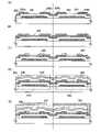
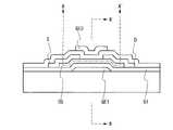
図1(A)に、本実施の形態の半導体装置の上面図を示す。図1(A)は、第1の基板1
210にFPCを貼り付ける前の液晶表示装置の上面図であり、図1(B)は、図1(A
)のG-Hの断面図を示し、導電粒子と接続配線の接続領域を示している。図1(C)は
図1(A)のE-Fの断面図を示し、画素部と接続配線の接続領域を示している。FIG. 1A shows a top view of a semiconductor device of this embodiment. FIG. 1A shows the
FIG. 1B is a top view of the liquid crystal display device before attaching an FPC to 210, and FIG.
) is a cross-sectional view taken along line GH, showing the connection region between the conductive particles and the connection wiring. FIG. 1C is a cross-sectional view taken along EF in FIG. 1A, showing a connection region between a pixel portion and a connection wiring.
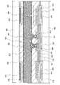
画素電極層が形成されたアクティブマトリクス基板となる第1の基板1210と第1の対
向電極層1291、第2の対向電極層1292が形成された第2の基板1204がシール
材1205により貼り合わされており、シール材1205の内部に液晶1280が充填さ
れている。第1の基板1210上には信号線駆動回路部1200、走査線駆動回路部12
01、及び画素電極層がマトリクス状に形成された画素部1202が形成されている。A
01, and a
駆動回路部の上に設けられる第2の対向電極層1292は、第1の対向電極層1291と
異なる電位である。画素部1202の上に設けられる第1の対向電極層1291と駆動回
路部の上に設けられる第2の対向電極層1292とは、別々の電極層として電気的に接続
されておらず、それぞれ異なる電位とする。A second
画素電極層に印加される電位(電圧)は、画素用薄膜トランジスタを介して印加されるた
め、画素電極層の電圧は、実際に画素用薄膜トランジスタを介して印加する電圧より数ボ
ルト低い可能性がある。よって、第1の対向電極層1291に印加する電位(電圧)もそ
の差分を考慮して印加する電圧値を設定することが好ましい。Since the potential (voltage) applied to the pixel electrode layer is applied via the pixel thin film transistor, the voltage of the pixel electrode layer may be several volts lower than the voltage actually applied via the pixel thin film transistor. . Therefore, it is preferable to set the potential (voltage) applied to the first
第1の基板1210上に設けられた信号線駆動回路部1200は駆動回路用薄膜トランジ
スタ1223を有する回路を備えている。A signal line
画素部1202は、画素用薄膜トランジスタ1211を有する。また、絶縁層1214上
及び絶縁層1214に形成された開口内には画素用薄膜トランジスタ1211に接続する
画素電極層1250が形成される。The
画素用薄膜トランジスタ1211、駆動回路用薄膜トランジスタ1223は、酸化物半導
体層、ゲート絶縁層、並びにゲート電極層で構成され、駆動回路用薄膜トランジスタ12
23は絶縁層1214を介してゲート電極層及び酸化物半導体層と重なる導電層1293
を上方に配置している。The pixel
23 is a
is placed above.
駆動回路用薄膜トランジスタ1223において、酸化物半導体層をゲート電極層と導電層
1293で挟み込む構成とすることにより、駆動回路用薄膜トランジスタ1223のしき
い値ばらつきを低減させることができ、安定した電気特性を有する駆動回路用薄膜トラン
ジスタ1223を備えた半導体装置を提供することができる。導電層1293は、ゲート
電極層と同電位としても良いし、フローティング電位でも良いし、固定電位、例えばGN
D電位や0Vでもよい。また、導電層1293に任意の電位を与えることで、一対の基板
の間隔にもよるが、駆動回路用薄膜トランジスタ1223のしきい値を制御することもで
きる。In the driver circuit
D potential or 0V may be used. By applying an arbitrary potential to the
導電層1293は、ゲート電極層及び半導体層と重なった領域に選択的に設けられるよう
に、開口を有するパターンに加工してもよい。The
また、駆動回路部上に設けられる第2の対向電極層1292は、平板状のパターンであり
、開口を有するパターンに加工してもよい。第2の対向電極層1292を開口を有するパ
ターンに加工することによって駆動回路部に設けられる薄膜トランジスタを構成する導電
層との間に形成される寄生容量を軽減することもできる。よって、半導体装置の低消費電
力化を実現できる。In addition, the second
本明細書において、駆動回路部上における第2の対向電極層1292が有する開口パター
ン(スリット)とは、閉空間に開口されたパターンの他、一部開かれた屈曲部や枝分かれ
した櫛歯状のようなパターンも含まれるものとする。In this specification, the opening patterns (slits) of the second
第1の基板1210及び第2の基板1204としては、アルミノシリケートガラス、アル
ミノホウケイ酸ガラス、バリウムホウケイ酸ガラスのような電子工業用に使われるガラス
基板(「無アルカリガラス基板」とも呼ばれる)、石英基板、セラミック基板、プラスチ
ック基板等を適宜用いることができる。第1の基板1210及び第2の基板1204とし
て、可撓性を有するプラスチック基板を用いることで、可撓性を有する半導体装置を作製
することができる。As the
シール材1205は、スクリーン印刷法、インクジェット装置またはディスペンス装置を
用いて第1の基板1210または第2の基板1204上に塗布する。シール材1205は
、代表的には可視光硬化性、紫外線硬化性または熱硬化性の樹脂を含む材料を用いること
ができる。例えば、ビスフェノールA型液状樹脂、ビスフェノールA型固形樹脂、含ブロ
ムエポキシ樹脂、ビスフェノールF型樹脂、ビスフェノールAD型樹脂、フェノール型エ
ポキシ樹脂、クレゾール型エポキシ樹脂、ノボラック型エポキシ樹脂、環状脂肪族エポキ
シ樹脂、エピビス型エポキシ樹脂、グリシジルエステル樹脂、グリシジルアミン樹脂、複
素環式エポキシ樹脂、変性エポキシ樹脂等のエポキシ樹脂を用いることができる。シール
材1205としては粘度40~400Pa・sのものを硬化して用いる。また、フィラー
(直径1μm~24μm)を含んでもよい。なお、シール材としては、後に接する液晶に
溶解しないシール材料を選択することが好ましい。The
導電粒子1270として、絶縁性球体に金属薄膜が被覆された導電粒子を用いることがで
きる。絶縁性球体は、シリカガラス、硬質樹脂等で形成される。金属薄膜は、金、銀、パ
ラジウム、ニッケル、酸化インジウムスズ(ITO)、及び酸化インジウム亜鉛(IZO
)の単層または積層構造とすることができる。例えば、金属薄膜として金薄膜や、ニッケ
ル薄膜及び金薄膜の積層等を用いることができる。絶縁性球体を中心に有する導電粒子1
270を用いることで、弾性が高まり、外部からの圧力に対する破壊の可能性を抑えるこ
とができる。As the
) can be a single layer or laminated structure. For example, a gold thin film, a laminate of a nickel thin film and a gold thin film, or the like can be used as the metal thin film.
By using 270, the elasticity is increased and the possibility of breakage due to external pressure can be suppressed.
画素電極層1250の材料は、透過型の液晶表示装置の場合と反射型の液晶表示装置で異
なる。透過型液晶表示装置の場合、画素電極層1250は透光性を有する材料を用いて形
成する。透光性を有する材料とは、酸化インジウムスズ(ITO)、酸化亜鉛(ZnO)
、酸化インジウム亜鉛(IZO)、ガリウムを添加した酸化亜鉛(GZO)等がある。The material of the
, indium zinc oxide (IZO), gallium-doped zinc oxide (GZO), and the like.
また、画素電極層1250として、導電性高分子材料(導電性ポリマーともいう)を含む
導電性組成物を用いて形成することができる。導電性組成物を用いて形成した画素電極層
は、シート抵抗が10000Ω/□以下、波長550nmにおける透光率が70%以上で
あることが好ましい。また、導電性組成物に含まれる導電性高分子材料の抵抗率が0.1
Ω・cm以下であることが好ましい。Alternatively, the
It is preferably Ω·cm or less.
導電性高分子材料としては、いわゆるπ電子共役系導電性高分子が用いることができる。
例えば、ポリアニリンまたはその誘導体、ポリピロールまたはその誘導体、ポリチオフェ
ンまたはその誘導体、若しくはこれらの2種以上の共重合体などがあげられる。As the conductive polymer material, a so-called π-electron conjugated conductive polymer can be used.
Examples include polyaniline or derivatives thereof, polypyrrole or derivatives thereof, polythiophene or derivatives thereof, or copolymers of two or more of these.
一方、反射型の液晶表示装置の場合、画素電極層1250は反射率の高い金属電極が用い
られる。具体的には、アルミニウム、銀等が用いられる。また、画素電極層1250の表
面を凹凸状にすることで、反射率が高まる。このため、画素電極層1250の下の絶縁層
1214を凹凸とすればよい。On the other hand, in the case of a reflective liquid crystal display device, a metal electrode with high reflectance is used for the
また、半透過型の液晶表示装置の場合には、画素電極層は透過型の材料と反射型の材料が
用いられる。In the case of a semi-transmissive liquid crystal display device, a transmissive material and a reflective material are used for the pixel electrode layer.
また、第1の基板1210の端部には、端子部1240が形成される。端子部1240に
は、接続配線1208上に接続端子1241が形成される。A
図1(B)は、導電粒子1270と接続端子1241とが接続される領域の断面図である
。第1の基板1210上に接続配線1208が形成される。接続配線1208上には画素
電極層1250と同時に形成される接続端子1241が形成される。接続端子1241は
、接続配線1208及び導電粒子1270を介して、第1の対向電極層1291と電気的
に接続される。また、接続端子1241はFPC(図示せず)と接続される。なお、図1
(B)において、導電粒子1270は樹脂層1235によって固定されている。樹脂層1
235としては、シール材1205で用いるような有機樹脂絶縁材料を用いることができ
る。FIG. 1B is a cross-sectional view of a region where
In (B),
As 235, an organic resin insulating material such as that used for the sealing
図1(C)は、画素電極層1250と接続端子1243とが接続される領域の断面図であ
る。第1の基板1210上に画素用薄膜トランジスタ1211ならびに駆動回路用薄膜ト
ランジスタ1223のソース電極層及びドレイン電極層と同時に形成される接続配線12
42が形成される。接続配線1242上には画素電極層1250と同時に形成される接続
端子1243が形成される。接続端子1243は、接続配線1242を介して、画素電極
層1250と電気的に接続される。なお、本実施の形態では、アクティブマトリクス型の
液晶表示装置の形態を用いているため、画素電極層1250と接続配線1242は直接接
続せず、画素用薄膜トランジスタ1211、または信号線駆動回路部1200中の薄膜ト
ランジスタを介して接続する。FIG. 1C is a cross-sectional view of a region where the
42 are formed. A
そして、画素電極層1250上に第1の配向膜1206が設けられ、ラビング処理が施さ
れる。この第1の配向膜1206およびラビング処理は、使用する液晶のモードにより必
要な場合と不必要な場合がある。Then, a
対向基板となる第2の基板1204には、信号線駆動回路部1200と重なる位置にブラ
ックマトリクス、画素部1202と重なる位置にカラーフィルタ、さらに保護層などを設
けてもよい。カラー表示をフィールドシーケンシャルと言われる色順次方式で表示する場
合にはカラーフィルタは設けなくともよい。また、対向基板となる第2の基板1204に
は、第1の対向電極層1291と第2の対向電極層1292が形成され、第1の対向電極
層1291上に第2の配向膜1207が設けられ、ラビング処理が施される。この第2の
基板1204も第1の基板1210と同様に、使用する液晶のモードにより配向膜および
ラビング処理が必要な場合と不必要な場合がある。A
また、配向膜を用いないブルー相を示す液晶を用いてもよい。ブルー相は液晶相の一つで
あり、コレステリック液晶を昇温していくと、コレステリック相から等方相へ転移する直
前に発現する相である。ブルー相は狭い温度範囲でしか発現しないため、温度範囲を改善
するために5重量%以上のカイラル剤を混合させた液晶組成物を液晶1280に用いる。
ブルー相を示す液晶とカイラル剤とを含む液晶組成物は、応答速度が1msec以下と短
く、光学的等方性であるため配向処理が不要であり、視野角依存性が小さい。Alternatively, a liquid crystal exhibiting a blue phase without using an alignment film may be used. The blue phase is one of the liquid crystal phases, and is a phase that appears immediately before the cholesteric phase transitions to the isotropic phase when the temperature of the cholesteric liquid crystal is increased. Since the blue phase is expressed only in a narrow temperature range, a liquid crystal composition in which 5% by weight or more of a chiral agent is mixed is used for the
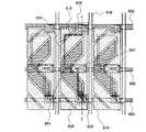
A liquid crystal composition containing a liquid crystal exhibiting a blue phase and a chiral agent has a short response time of 1 msec or less, is optically isotropic, does not require alignment treatment, and has low viewing angle dependency.
第1の対向電極層1291、及び第2の対向電極層1292が形成された第2の基板12
04または画素電極層1250が形成された第1の基板1210に、柱状スペーサー12
55が設けられる。柱状スペーサー1255は第1の基板1210と第2の基板1204
とのギャップを保持するためのものであり、本実施の形態では、第2の基板1204側に
設ける例を示す。この柱状スペーサー1255はフォトリソスペーサー、ポストスペーサ
ー、貝柱スペーサー、カラムスペーサーとも呼ばれている。なお球状のスペーサーを用い
ていても良い。本実施の形態では、柱状スペーサーを用いる。柱状スペーサー1255の
作製方法としては、感光性アクリルなどの有機絶縁材料を基板の全面にスピンコート法に
より塗布し、これを一連のフォトリソグラフィの工程を行うことにより、基板上に残った
感光性アクリルがスペーサーとしての役割を果たす。当該方法により、露光時のマスクパ
ターン次第でスペーサーを配置したい場所を露光できるため、液晶が駆動しない部分にこ
の柱状スペーサー1255を配置することにより、上下基板間のギャップを保持するだけ
でなく、液晶の光漏れも防ぐことができる。また、柱状スペーサー1255は、インクジ
ェット法により有機絶縁材料を含む組成物を吐出し焼成して形成することができる。
04 or the
55 are provided. A
In this embodiment mode, an example provided on the
導電粒子1270の周囲には樹脂層1235として有機樹脂絶縁材料ではなく、導電性ポ
リマーが充填されてもよい。導電性ポリマーの代表例としては、導電性ポリアニリン、導
電性ポリピロール、導電性ポリチオフェン、ポリエチレンジオキシチオフェン(PEDO
T)とポリスチレンスルホン酸(PSS)の混合物が挙げられる。また、画素電極層12
50に用いることが可能な導電性ポリマーに列挙したものを適宜用いることができる。導
電性ポリマーは、インクジェット装置、ディスペンサ装置等で導電性ポリマーを塗布して
形成する。第2の対向電極層1292または接続配線1208に導電性ポリマーが接して
いることにより、導電粒子1270と導電性ポリマーが接し、第2の対向電極層1292
及び接続配線1208の接続抵抗を低減することが可能である。The periphery of the
T) and polystyrene sulfonic acid (PSS) mixtures. In addition, the
Those listed in the conductive polymer that can be used in 50 can be used as appropriate. The conductive polymer is formed by applying a conductive polymer using an inkjet device, a dispenser device, or the like. Since the conductive polymer is in contact with the second
And the connection resistance of the
なお、接続配線1208と、第2の基板1204上に形成される第1の対向電極層129
1が導電粒子1270を介して導通する。また、接続配線1246と、第2の基板120
4上に形成される第2の対向電極層1292が導電粒子1270を介して導通する。また
、接続配線1246と接続配線1208は異なる電位である。Note that the
1 conducts through the
The second
また、導電粒子1270として、有機薄膜で被覆された導電性材料よりなるナノ粒子を用
いてもよい。このようなナノ粒子を用いた場合、第1の基板1210及び第2の基板12
04を貼りあわせた後、シール材の硬化及び液晶の再配向のための加熱工程により有機薄
膜が分解され、導電性材料よりなるナノ粒子同士が接触し融着することで、導電粒子を形
成することができる。Also, as the
After bonding 04, the organic thin film is decomposed by the heating process for curing the sealing material and reorienting the liquid crystal, and the nanoparticles made of the conductive material contact and fuse to form conductive particles. be able to.
ナノ粒子は、液滴吐出法を用いて吐出される。液滴吐出法とは所定の物質を含む液滴を細
孔から吐出してパターンを形成する方法であり、ここでは溶媒に有機薄膜で被覆された導
電性材料よりなるナノ粒子が分散された組成物を液滴として吐出(噴出)し、乾燥するこ
とで該溶媒を気化する。The nanoparticles are ejected using a droplet ejection method. The droplet ejection method is a method of ejecting droplets containing a predetermined substance from pores to form a pattern. The solvent is vaporized by ejecting (jetting) the substance as droplets and drying.
ナノ粒子を形成する導電性材料には、金(Au)、銀(Ag)、白金(Pt)、ニッケル
(Ni)、銅(Cu)、パラジウム(Pd)、タンタル(Ta)、イリジウム(Ir)、
ロジウム(Rh)、タングステン(W)、アルミニウム(Al)等から選択された金属元
素又はこれらの元素を主成分とする合金材料が用いられる。また、カドミウム(Cd)、
亜鉛(Zn)の金属硫化物、鉄(Fe)、チタン(Ti)、ゲルマニウム(Ge)、ケイ
素(Si)、ジルコニウム(Zr)、バリウム(Ba)などの酸化物、ハロゲン化銀の一
種又は複数種が混合されていてもよい。なお、導電性材料に2種以上の元素もしくは化合
物が用いられる場合、その混合状態については特に限定されず、例えばこれらの各々が均
一に存在しても、中心部にいずれか一が偏在していても良い。また、ナノ粒子は、少なく
とも表面が導電性材料より形成されていれば良く、内部が絶縁性を有する物質であっても
良い。Conductive materials forming nanoparticles include gold (Au), silver (Ag), platinum (Pt), nickel (Ni), copper (Cu), palladium (Pd), tantalum (Ta), iridium (Ir), ,
Metal elements selected from rhodium (Rh), tungsten (W), aluminum (Al), etc., or alloy materials containing these elements as main components are used. Also, cadmium (Cd),
One or more of metal sulfides of zinc (Zn), oxides such as iron (Fe), titanium (Ti), germanium (Ge), silicon (Si), zirconium (Zr), barium (Ba), silver halide Seeds may be mixed. When two or more elements or compounds are used in the conductive material, the mixed state is not particularly limited. can be Moreover, the nanoparticles may be made of a conductive material at least on the surface, and may be made of an insulating substance inside.
ナノ粒子の粒径は、1nm以上200nm以下、好ましくは1nm以上100nm以下が
良く、吐出材料に含まれるナノ粒子の粒径は均一であるほうが好ましい。The particle size of the nanoparticles is preferably 1 nm or more and 200 nm or less, preferably 1 nm or more and 100 nm or less, and the nanoparticles contained in the ejection material preferably have a uniform particle size.
なお、ナノ粒子を構成する導電性材料によっては電圧を印加した際、粒子間にボイドが発
生することがある。これは、導電性材料の結晶成長が非常に速く進行するためであり、液
晶表示装置への印加電圧を低く設定することやナノ粒子に合金材料を用いることでこのよ
うなボイドの発生を抑制することができる。よって、より信頼性の高い液晶表示装置を得
ることができる。Depending on the conductive material forming the nanoparticles, voids may occur between the particles when a voltage is applied. This is because the crystal growth of the conductive material progresses very quickly, and the occurrence of such voids is suppressed by setting a low voltage applied to the liquid crystal display device or by using an alloy material for the nanoparticles. be able to. Therefore, a more reliable liquid crystal display device can be obtained.
ナノ粒子を被覆する有機薄膜は、溶媒中においてナノ粒子の凝集を防ぎ、粒子を安定に分
散させる機能を有する分散剤に相当する。そのため、有機薄膜を形成する化合物は、導電
性材料が有する金属元素と配位結合を形成することが可能な物質や界面活性剤等により構
成されている。ここで、金属元素と配位結合を形成する物質としては、アミノ基、チオー
ル基(-SH)、スルフィド基(-S-)、ヒドロキシ基(-OH)、エーテル基(-O
-)、カルボキシル基(-COOH)、シアノ基(-CN)等の窒素、硫黄、酸素原子な
どが有する孤立電子対を有する物質が挙げられる。例えば、エタノールアミン等のヒドロ
キシアミン類、ポリエチレンイミン等のアミン化合物、ポリビニルピロリドン等のアミド
化合物、ポリビニルアルコール等のアルコール類、アルカンチオール類、ジチオール類、
エチレングリコール、ジエチレングリコール等のグリコール類、ポリエチレングリコール
等のエーテル類、ポリアクリル酸やカルボキシメチルセルロース等を用いることができる
。また、界面活性剤としては、例えば、ビス(2-エチルヘキシル)スルホコハク酸ナト
リウムやドデシルベンゼンスルホン酸ナトリウム等のアニオン性界面活性剤、ポリアルキ
ルグルコールのアルキルエステルやアルキルフェニルエーテル等の非イオン性界面活性剤
、フッ素界面活性剤、エチレンイミンとエチレンオキサイドとの共重合体等を用いること
ができる。なお、分散剤はナノ粒子に対し30wt%以上とした場合には吐出材料の粘度
が高くなるため、1.0wt%以上30wt%以下が好ましい。The organic thin film that coats the nanoparticles corresponds to a dispersant that has the function of preventing aggregation of the nanoparticles in a solvent and stably dispersing the particles. Therefore, the compound forming the organic thin film is composed of a substance capable of forming a coordinate bond with the metal element of the conductive material, a surfactant, or the like. Here, the substance that forms a coordinate bond with the metal element includes an amino group, a thiol group (-SH), a sulfide group (-S-), a hydroxy group (-OH), an ether group (-O
-), a carboxyl group (-COOH), a cyano group (-CN), and other substances having a lone pair of electrons with nitrogen, sulfur, oxygen atoms, and the like. For example, hydroxyamines such as ethanolamine, amine compounds such as polyethyleneimine, amide compounds such as polyvinylpyrrolidone, alcohols such as polyvinyl alcohol, alkanethiols, dithiols,
Glycols such as ethylene glycol and diethylene glycol, ethers such as polyethylene glycol, polyacrylic acid, carboxymethyl cellulose, and the like can be used. Examples of surfactants include anionic surfactants such as sodium bis(2-ethylhexyl)sulfosuccinate and sodium dodecylbenzenesulfonate, and nonionic surfactants such as alkylesters and alkylphenylethers of polyalkylglycols. Active agents, fluorosurfactants, copolymers of ethyleneimine and ethylene oxide, and the like can be used. Note that if the dispersant is 30 wt % or more with respect to the nanoparticles, the viscosity of the ejection material increases, so the content is preferably 1.0 wt % or more and 30 wt % or less.
上記のような有機薄膜で被覆された導電性材料よりなるナノ粒子は溶媒に分散されて吐出
される。溶媒には、水または有機溶媒を用いることができ、有機溶媒は水溶性有機溶媒で
あっても、非水溶性有機溶媒であっても良い。例えば、水溶性有機溶剤にはメタノール、
エタノール、プロパノール、ブチルアルコール、グリセリン、ジプロピレングリコール、
エチレングレコール等のアルコール、アセトン、メチルエチルケトン等のケトン、エチレ
ングリコールモノメチルエーテル、エチレングリコールモノエチルエーテル、エチレング
リコールモノブチルエーテル、ジエチレングリコールモノブチルエーテル等のグリコール
エーテル、2-ピロリドン、N-メチルピロリドン等の水溶性含窒素有機化合物等が挙げ
られる。また、非水溶性有機溶媒には、酢酸エーテル等のエステル類、オクタン、ノナン
、デカン等の直鎖アルカン、あるいはシクロヘキサンなどのシクロアルカン、トルエン、
キシレン、ベンゼン、ジクロロベンゼン等の芳香族化合物等がある。もちろん、これら溶
媒は必ずしも一種で使用する必要はなく、溶媒同士において相分離が生じなければ複数種
を混合して用いることも可能である。Nanoparticles made of a conductive material coated with an organic thin film as described above are dispersed in a solvent and discharged. Water or an organic solvent can be used as the solvent, and the organic solvent may be a water-soluble organic solvent or a non-water-soluble organic solvent. For example, water-soluble organic solvents include methanol,
ethanol, propanol, butyl alcohol, glycerin, dipropylene glycol,
alcohols such as ethylene glycol; ketones such as acetone and methyl ethyl ketone; glycol ethers such as ethylene glycol monomethyl ether, ethylene glycol monoethyl ether, ethylene glycol monobutyl ether and diethylene glycol monobutyl ether; Examples include nitrogen-containing organic compounds. Examples of water-insoluble organic solvents include esters such as ether acetate, linear alkanes such as octane, nonane and decane, cycloalkanes such as cyclohexane, toluene,
aromatic compounds such as xylene, benzene, dichlorobenzene; Of course, it is not always necessary to use one kind of these solvents, and it is also possible to use a mixture of plural kinds of solvents as long as phase separation does not occur between the solvents.
シール材1205及び導電粒子1270を、第1の基板1210上または第2の基板12
04上に吐出し、その後、シール材1205の内側に液晶を吐出する。この後、第1の基
板1210及び第2の基板1204を減圧雰囲気で貼り合せ、UV光を照射してシール材
1205を硬化した後、加熱してシール材1205を更に硬化して第1の基板1210及
び第2の基板1204を固着する。また、当該加熱により、液晶の配向を均一にする。A
04, and then the liquid crystal is discharged inside the sealing
この結果、第1の基板1210と第2の基板1204を貼り合わせることができる。As a result, the
そして、第1の基板1210と、第2の基板1204がパネルの形に分断される。さらに
、コントラストを高めるために第1の基板1210の外側に第1偏光板1290と、第2
の基板1204の外側に第2偏光板1295が設けられている。なお、反射型の表示装置
の場合には第1偏光板1290が必要ない場合がある。Then, the
A second
また、本実施の形態では図示しないが、ブラックマトリクス(遮光層)、位相差部材、反
射防止部材などの光学部材(光学基板)などは適宜設ける。例えば、偏光基板及び位相差
基板による円偏光を用いてもよい。また、光源としてバックライト、サイドライトなどを
用いてもよい。Although not shown in this embodiment mode, an optical member (optical substrate) such as a black matrix (light shielding layer), a retardation member, and an antireflection member is provided as appropriate. For example, circularly polarized light using a polarizing substrate and a retardation substrate may be used. Moreover, a backlight, a sidelight, or the like may be used as the light source.
アクティブマトリクス型の液晶表示装置においては、マトリクス状に配置された画素電極
を駆動することによって、画面上に表示パターンが形成される。詳しくは選択された画素
電極と該画素電極に対応する対向電極との間に電圧が印加されることによって、画素電極
と対向電極との間に配置された液晶層の光学変調が行われ、この光学変調が表示パターン
として観察者に認識される。In an active matrix liquid crystal display device, a display pattern is formed on a screen by driving pixel electrodes arranged in a matrix. Specifically, by applying a voltage between the selected pixel electrode and the counter electrode corresponding to the pixel electrode, the liquid crystal layer arranged between the pixel electrode and the counter electrode is optically modulated. An observer perceives the optical modulation as a display pattern.
液晶表示装置の動画表示において、液晶分子自体の応答が遅いため、残像が生じる、また
は動画のぼけが生じるという問題がある。液晶表示装置の動画特性を改善するため、全面
黒表示を1フレームおきに行う、所謂、黒挿入と呼ばれる駆動技術がある。2. Description of the Related Art When displaying a moving image on a liquid crystal display device, there is a problem that an afterimage occurs or a moving image blurs due to the slow response of the liquid crystal molecules themselves. In order to improve the moving image characteristics of a liquid crystal display device, there is a driving technique called so-called black insertion, in which a full black display is performed every other frame.
また、垂直同期周波数を通常の1.5倍、好ましくは2倍以上にすることで応答速度を改
善するとともに各フレーム内の分割された複数フィールド毎に書き込む階調を選択する、
所謂、倍速駆動と呼ばれる駆動技術もある。In addition, by increasing the vertical synchronization frequency to 1.5 times the normal frequency, preferably 2 times or more, the response speed is improved and the gradation to be written is selected for each of the divided multiple fields within each frame.
There is also a driving technique called so-called double speed driving.
また、液晶表示装置の動画特性を改善するため、バックライトとして複数のLED(発光
ダイオード)光源または複数のEL光源などを用いて面光源を構成し、面光源を構成して
いる各光源を独立して1フレーム期間内で間欠点灯駆動する駆動技術もある。面光源とし
て、3種類以上のLEDを用いてもよいし、白色発光のLEDを用いてもよい。独立して
複数のLEDを制御できるため、液晶層の光学変調の切り替えタイミングに合わせてLE
Dの発光タイミングを同期させることもできる。この駆動技術は、LEDを部分的に消灯
することができるため、特に一画面を占める黒い表示領域の割合が多い映像表示の場合に
は、消費電力の低減効果が図れる。In addition, in order to improve the moving image characteristics of the liquid crystal display device, a surface light source is configured using a plurality of LED (light emitting diode) light sources or a plurality of EL light sources as a backlight, and each light source constituting the surface light source is independent. There is also a driving technique for performing intermittent lighting driving within one frame period. As the surface light source, three or more types of LEDs may be used, or white light emitting LEDs may be used. Since multiple LEDs can be controlled independently, the LEDs can be adjusted according to the switching timing of the optical modulation of the liquid crystal layer.
The light emission timing of D can also be synchronized. Since this driving technique can partially turn off the LEDs, it is possible to reduce power consumption particularly in the case of image display in which a large percentage of black display areas occupy one screen.
これらの駆動技術を組み合わせることによって、液晶表示装置の動画特性などの表示特性
を従来よりも改善することができる。By combining these driving techniques, it is possible to improve the display characteristics such as moving image characteristics of the liquid crystal display device compared to the conventional ones.
本発明の一実施形態では、駆動回路部上に対向電極層を設けることにより、薄膜トランジ
スタの静電破壊を防ぐことができるが、さらに保護回路を設けてもよい。保護回路は、酸
化物半導体層を用いた非線形素子を用いて構成することが好ましい。例えば、保護回路は
画素部と、走査線入力端子及び信号線入力端子との間に配設されている。本実施の形態で
は複数の保護回路を配設して、走査線、信号線及び容量バス線に静電気等によりサージ電
圧が印加され、画素トランジスタなどが破壊されないように構成されている。そのため、
保護回路にはサージ電圧が印加されたときに、共通配線に電荷を逃がすように構成する。
また、保護回路は、走査線に対して並列に配置された非線形素子によって構成されている
。非線形素子は、ダイオードのような二端子素子又はトランジスタのような三端子素子で
構成される。例えば、画素部の薄膜トランジスタと同じ工程で形成することも可能であり
、例えばゲート端子とドレイン端子を接続することによりダイオードと同様の特性を持た
せることができる。In one embodiment of the present invention, electrostatic breakdown of the thin film transistor can be prevented by providing a counter electrode layer on the drive circuit portion, but a protection circuit may be provided. The protection circuit is preferably formed using a nonlinear element using an oxide semiconductor layer. For example, the protection circuit is arranged between the pixel portion and the scanning line input terminal and the signal line input terminal. In this embodiment, a plurality of protection circuits are provided to prevent damage to pixel transistors and the like caused by surge voltages caused by static electricity or the like being applied to scanning lines, signal lines, and capacitor bus lines. for that reason,
The protective circuit is configured to release electric charges to the common wiring when a surge voltage is applied.
Also, the protection circuit is composed of a nonlinear element arranged in parallel with the scanning line. The non-linear element may consist of a two-terminal element such as a diode or a three-terminal element such as a transistor. For example, it can be formed in the same process as the thin film transistor in the pixel portion, and by connecting the gate terminal and the drain terminal, for example, it can have the same characteristics as a diode.
以上のように、酸化物半導体層を用いる薄膜トランジスタを有する液晶表示装置であって
、且つ、静電気に対して強く、低消費電力の液晶表示装置を提供することができる。As described above, a liquid crystal display device including a thin film transistor including an oxide semiconductor layer, which is resistant to static electricity and consumes low power can be provided.
(実施の形態2)
実施の形態1で示す、第1の基板と第2の基板の間に液晶層を封入する半導体装置におい
て、第2の基板に設けられた対向電極層(第1の対向電極層及び第2の対向電極層)と接
続配線を電気的に接続するための接続領域に共通接続部を第1の基板上に形成する他の例
を示す。なお、第1の基板にはスイッチング素子として薄膜トランジスタが形成されてお
り、共通接続部の作製工程を画素部のスイッチング素子の作製工程と共通化させることで
工程を複雑にすることなく共通接続部を形成する。(Embodiment 2)
In the semiconductor device described in
本実施の形態では、共通接続部は、第1の基板と第2の基板とを接着するためのシール材
と重なる位置に配置され、シール材に含まれる導電粒子を介して対向電極層と電気的な接
続が行われる例を示す。或いは、図1(A)に示したように、画素部の外側であり、かつ
シール材と重ならない箇所に共通接続部を設け、共通接続部に重なるように導電粒子を含
むペーストをシール材とは別途設けて、対向電極層と電気的な接続が行われる。In this embodiment mode, the common connection portion is arranged at a position overlapping the sealing material for bonding the first substrate and the second substrate, and electrically connects the counter electrode layer with the conductive particles contained in the sealing material. Here is an example where a typical connection is made. Alternatively, as shown in FIG. 1A, a common connection portion is provided outside the pixel portion and does not overlap with the sealant, and a paste containing conductive particles is applied as the sealant so as to overlap the common connection portion. is provided separately and electrically connected to the counter electrode layer.
図2(A)は薄膜トランジスタと共通接続部とを同一基板(第1の基板300)上に作製
する半導体装置の断面構造図を示す図である。FIG. 2A is a cross-sectional structural view of a semiconductor device in which a thin film transistor and a common connection portion are manufactured over the same substrate (first substrate 300).
図2(A)において、画素電極層327と電気的に接続する薄膜トランジスタ320は、
画素部に設けられるチャネルエッチ型の薄膜トランジスタである。In FIG. 2A, the
It is a channel-etched thin film transistor provided in a pixel portion.
また、図2(B)は共通接続部の上面図の一例を示す図であり、図中の鎖線A1-A2が
図2(A)の共通接続部の断面に相当する。なお、図2(B)において図2(A)と同一
の部分には同じ符号を用いて説明する。FIG. 2B is a diagram showing an example of a top view of the common connection portion, and the dashed line A1-A2 in the drawing corresponds to the cross section of the common connection portion in FIG. 2A. In addition, in FIG. 2B, the same parts as those in FIG. 2A are denoted by the same reference numerals.
共通電位線310は、ゲート絶縁層302上に設けられ、薄膜トランジスタ320のソー
ス電極層及びドレイン電極層と同じ材料及び同じ工程で作製される。The common
また、共通電位線310は、保護絶縁層303で覆われ、保護絶縁層303は、共通電位
線310と重なる位置に複数の開口部を有している。この開口部は、薄膜トランジスタ3
20のドレイン電極層と画素電極層327とを接続するコンタクトホールと同じ工程で作
製される。Also, the common
The contact hole connecting the drain electrode layer 20 and the
なお、ここでは面積が大きく異なるため、画素部におけるコンタクトホールと、共通接続
部の開口部と使い分けて呼ぶこととする。また、図2(A)では、画素部と共通接続部と
で同じ縮尺で図示しておらず、例えば共通接続部の鎖線A1-A2の長さが500μm程
度であるのに対して、薄膜トランジスタの幅は50μm未満であり、実際には10倍以上
面積が大きいが、分かりやすくするため、図2(A)に画素部と共通接続部の縮尺をそれ
ぞれ変えて図示している。Note that the contact holes in the pixel portion and the openings of the common connection portion are separately called because the areas differ greatly here. In addition, in FIG. 2A, the pixel portion and the common connection portion are not shown on the same scale. The width is less than 50 .mu.m, and the actual area is ten times or more larger. However, the scales of the pixel portion and the common connection portion are changed in FIG. 2A for easy understanding.
また、共通電極層306は、保護絶縁層303上に設けられ、画素部の画素電極層327
と同じ材料及び同じ工程で作製される。In addition, the
made from the same materials and processes as
このように、画素部のスイッチング素子の作製工程と共通させて共通接続部の作製工程を
行う。In this manner, the manufacturing process of the common connection portion is performed in common with the manufacturing process of the switching element of the pixel portion.
そして画素部と共通接続部が設けられた第1の基板と、対向電極層を有する第2の基板と
をシール材を用いて固定する。Then, the first substrate provided with the pixel portion and the common connection portion and the second substrate having the counter electrode layer are fixed using a sealing material.
シール材に導電粒子を含ませる場合は、シール材と共通接続部が重なるように第1の基板
と第2の基板の位置合わせが行われる。例えば、小型の液晶パネルにおいては、画素部の
対角に2個の共通接続部がシール材と重ねて配置される。また、大型の液晶パネルにおい
ては、4個以上の共通接続部がシール材と重ねて配置される。When the sealing material contains conductive particles, the first substrate and the second substrate are aligned so that the sealing material and the common connection portion overlap each other. For example, in a small-sized liquid crystal panel, two common connection portions are arranged diagonally on the pixel portion so as to overlap the sealing material. Moreover, in a large-sized liquid crystal panel, four or more common connection portions are arranged so as to overlap with the sealing material.
なお、共通電極層306は、シール材に含まれる導電粒子と接触する電極であり、第2の
基板の対向電極層と電気的に接続が行われる。Note that the
液晶注入法を用いる場合は、シール材で第1の基板と第2の基板を固定した後、液晶を第
1の基板と第2の基板の間に注入する。また、液晶滴下法を用いる場合は、第2の基板或
いは第1の基板上にシール材を描画し、液晶を滴下させた後、減圧下で第1の基板と第2
の基板を貼り合わせる。When the liquid crystal injection method is used, the first substrate and the second substrate are fixed with a sealing material, and then liquid crystal is injected between the first substrate and the second substrate. In the case of using the liquid crystal dropping method, a sealing material is drawn on the second substrate or the first substrate, liquid crystal is dropped, and then the first substrate and the second substrate are placed under reduced pressure.
and paste the substrates together.
なお、本実施の形態では、対向電極層と電気的に接続する共通接続部の例を示したが、こ
の構造は対向電極層と共通接続部の接続に限定されず、対向電極層を他の配線や外部接続
端子などと接続する接続部に用いることができる。Note that although an example of the common connection portion electrically connected to the counter electrode layer is shown in this embodiment mode, this structure is not limited to the connection between the counter electrode layer and the common connection portion, and the counter electrode layer can be used in other ways. It can be used as a connecting portion for connecting to wiring, an external connection terminal, or the like.
本実施の形態は実施の形態1と自由に組み合わせることができる。This embodiment mode can be freely combined with the first embodiment mode.
(実施の形態3)
実施の形態2では、共通電位線としてソース電極層及びドレイン電極層と同じ材料及び同
じ工程で形成される配線を用いて共通接続部を作製する例を示したが、本実施の形態では
、図2とは異なる共通接続部の例を示す。(Embodiment 3)
In Embodiment 2, an example in which a common connection portion is formed using a wiring formed using the same material and in the same process as the source electrode layer and the drain electrode layer as the common potential line is shown; 2 shows examples of common connections different from 2. FIG.
本実施の形態では、共通接続部にゲート配線と同じ材料及び同じ工程で形成される電極を
設け、その上に設ける共通電位線として、ドレイン電極層と同じ材料及び同じ工程で形成
される配線を用いて共通接続部を作製する例を図3(A)及び図3(B)に示す。In this embodiment mode, an electrode formed using the same material and using the same process as the gate wiring is provided in the common connection portion, and a wiring formed using the same material and using the same process as the drain electrode layer is used as the common potential line provided thereover. FIGS. 3(A) and 3(B) show an example of fabricating a common connection portion using these materials.
図3(B)は共通接続部の上面図の一例を示す図であり、図中の鎖線F1-F2が図3(
A)の共通接続部の断面に相当する。FIG. 3(B) is a diagram showing an example of a top view of the common connection portion, and the dashed lines F1-F2 in FIG.
It corresponds to the cross section of the common connection part of A).
なお、図3(A)に示すように実施の形態2と画素部の薄膜トランジスタの構造は、同一
であるため、図2(A)と同じ部分には同じ符号を用い、ここでは詳細な説明は省略する
こととする。Note that, as shown in FIG. 3A, the structure of the thin film transistor in the pixel portion is the same as that in Embodiment 2. Therefore, the same reference numerals are used for the same portions as in FIG. We omit it.
共通電極311は、第1の基板300上に設けられ、薄膜トランジスタ320のゲート電
極と同じ材料及び同じ工程で作製される。The common electrode 311 is provided over the
また、共通電極311は、ゲート絶縁層302及び保護絶縁層303で覆われ、ゲート絶
縁層302及び保護絶縁層303は、共通電極311と重なる位置に開口部を有している
。この開口部は、実施の形態2とは異なり、2層の絶縁膜の厚さに相当する深い開口部と
なる。なお、この開口部は、ドレイン電極層304と画素電極層327とを接続するコン
タクトホールと同じ工程でエッチングした後、さらにゲート絶縁層を選択的にエッチング
することで作製される。In addition, the common electrode 311 is covered with the
また、共通電位線305は、ゲート絶縁層302上に設けられ、ドレイン電極層304と
同じ材料及び同じ工程で作製される。Further, the common
また、共通電位線305は、保護絶縁層303で覆われ、保護絶縁層303は、共通電位
線305と重なる位置に複数の開口部を有している。この開口部は、ドレイン電極層30
4と画素電極層327とを接続するコンタクトホールと同じ工程で作製される。Also, the common
4 and the
また、共通電極層306は、保護絶縁層303上に設けられ、画素部の画素電極層327
と同じ材料及び同じ工程で作製される。In addition, the
made from the same materials and processes as
このように、画素部のスイッチング素子の作製工程と共通させて共通接続部の作製工程を
行う。In this manner, the manufacturing process of the common connection portion is performed in common with the manufacturing process of the switching element of the pixel portion.
そして画素部と共通接続部が設けられた第1の基板と、対向電極を有する第2の基板とを
シール材を用いて固定する。Then, the first substrate provided with the pixel portion and the common connection portion and the second substrate provided with the counter electrode are fixed using a sealing material.
また、本実施の形態においては、複数の導電性粒子をゲート絶縁層の開口部にのみ選択的
に配置する。即ち、共通電極層306と共通電極311とが接している領域に複数の導電
性粒子を配置する。共通電極311及び共通電位線305の両方と接触する共通電極層3
06は、導電性粒子と接触する電極であり、第2の基板の対向電極と電気的に接続が行わ
れる。Further, in this embodiment mode, a plurality of conductive particles are selectively arranged only in the openings of the gate insulating layer. That is, a plurality of conductive particles are arranged in a region where the
06 is an electrode that contacts the conductive particles and is electrically connected to the counter electrode of the second substrate.
液晶注入法を用いる場合は、シール材で一対の基板を固定した後、液晶を一対の基板間に
注入する。また、液晶滴下法を用いる場合は、第2の基板或いは第1の基板上にシール材
を描画し、液晶を滴下させた後、減圧下で一対の基板を貼り合わせる。When a liquid crystal injection method is used, a pair of substrates are fixed with a sealing material, and then liquid crystal is injected between the pair of substrates. In the case of using a liquid crystal dropping method, a sealing material is drawn on the second substrate or the first substrate, liquid crystal is dropped, and then the pair of substrates are bonded together under reduced pressure.
なお、本実施の形態では、対向電極と電気的に接続する共通接続部の例を示したが、この
構造は対向電極と共通接続部の接続に限定されず、対向電極を他の配線や外部接続端子な
どと接続する接続部に用いることができる。In this embodiment mode, an example of the common connection portion electrically connected to the counter electrode is shown, but this structure is not limited to the connection between the counter electrode and the common connection portion, and the counter electrode can be connected to another wiring or an external wiring. It can be used for a connection portion that connects to a connection terminal or the like.
本実施の形態は実施の形態1または実施の形態2と自由に組み合わせることができる。例
えば、実施の形態1に示した接続配線1208と接続配線1246は隣り合う配線であり
、それぞれの電位が異なり、異なる対向電極層と接続する構成となっている。一方の配線
と一方の対向電極層とを接続する構成を実施の形態2のソース電極層及びドレイン電極層
と同じ材料及び同じ工程で形成される共通電位線の構成として採用し、もう一方の配線と
もう一方の対向電極層とを接続する構成を本実施の形態のドレイン電極層と同じ材料及び
同じ工程で形成される共通電位線とすることで、短絡を防止し、配線間隔を狭めることが
できる。This embodiment mode can be freely combined with
(実施の形態4)
本実施の形態は、本明細書で開示する半導体装置に適用できる薄膜トランジスタの例を示
す。本実施の形態で示す薄膜トランジスタ410、420は、実施の形態1の駆動回路用
薄膜トランジスタ1223、画素用薄膜トランジスタ1211、実施の形態2または実施
の形態3の薄膜トランジスタ320として用いることができる。(Embodiment 4)
This embodiment mode shows an example of a thin film transistor that can be applied to the semiconductor device disclosed in this specification. The
本実施の形態の半導体装置及び半導体装置の作製方法の一形態を図4を用いて説明する。One embodiment of a semiconductor device and a method for manufacturing the semiconductor device of this embodiment will be described with reference to FIGS.
図4(A)乃至(E)に半導体装置の断面構造を示す。図4(D)に示す薄膜トランジス
タ410、420は、チャネルエッチ型と呼ばれるボトムゲート構造の一つであり逆スタ
ガ型薄膜トランジスタともいう。図4(D)において、薄膜トランジスタ410は駆動回
路用薄膜トランジスタであり、薄膜トランジスタ420は画素用薄膜トランジスタである
。4A to 4E show cross-sectional structures of semiconductor devices.
また、薄膜トランジスタ410、420はシングルゲート構造の薄膜トランジスタを用い
て説明したが、必要に応じて、チャネル形成領域を複数有するマルチゲート構造の薄膜ト
ランジスタも形成することができる。Further, although the
以下、図4(A)乃至(E)を用い、基板400上に薄膜トランジスタ410、420を
作製する工程を説明する。A process for manufacturing
まず、絶縁表面を有する基板400上に導電膜を形成した後、第1のフォトリソグラフィ
工程によりゲート電極層411、ゲート電極層421を形成する。なお、レジストマスク
をインクジェット法で形成してもよい。レジストマスクをインクジェット法で形成すると
フォトマスクを使用しないため、製造コストを低減できる。First, after a conductive film is formed over the
絶縁表面を有する基板400に使用することができる基板に大きな制限はないが、少なく
とも、後の加熱処理に耐えうる程度の耐熱性を有していることが必要となる。バリウムホ
ウケイ酸ガラスやアルミノホウケイ酸ガラスなどのガラス基板を用いることができる。There is no particular limitation on the substrate that can be used as the
また、ガラス基板としては、後の加熱処理の温度が高い場合には、歪み点が730℃以上
のものを用いると良い。また、ガラス基板には、例えば、アルミノシリケートガラス、ア
ルミノホウケイ酸ガラス、バリウムホウケイ酸ガラスなどのガラス材料が用いられている
。なお、酸化ホウ素と比較して酸化バリウム(BaO)を多く含ませることで、より実用
的な耐熱ガラスが得られる。このため、B2O3よりBaOを多く含むガラス基板を用い
ることが好ましい。Further, as the glass substrate, a glass substrate having a strain point of 730° C. or higher is preferably used when the temperature of the subsequent heat treatment is high. Glass materials such as aluminosilicate glass, aluminoborosilicate glass, and barium borosilicate glass are used for glass substrates. By containing more barium oxide (BaO) than boron oxide, more practical heat-resistant glass can be obtained. Therefore, it is preferable to use a glass substrate containing more BaO than B2 O3 .
なお、上記のガラス基板に代えて、セラミック基板、石英基板、サファイア基板などの絶
縁体でなる基板を用いても良い。他にも、結晶化ガラスなどを用いることができる。A substrate made of an insulator such as a ceramic substrate, a quartz substrate, or a sapphire substrate may be used instead of the glass substrate. In addition, crystallized glass or the like can be used.
下地膜となる絶縁膜を基板400とゲート電極層411、及びゲート電極層421との間
に設けてもよい。下地膜は、基板400からの不純物元素の拡散を防止する機能があり、
窒化珪素膜、酸化珪素膜、窒化酸化珪素膜、又は酸化窒化珪素膜から選ばれた一又は複数
の膜による積層構造により形成することができる。An insulating film serving as a base film may be provided between the
It can have a stacked structure of one or a plurality of films selected from a silicon nitride film, a silicon oxide film, a silicon nitride oxide film, and a silicon oxynitride film.
また、ゲート電極層411、及びゲート電極層421の材料は、モリブデン、チタン、ク
ロム、タンタル、タングステン、アルミニウム、銅、ネオジム、スカンジウム等の金属材
料又はこれらを主成分とする合金材料を用いて、単層で又は積層して形成することができ
る。The gate electrode layers 411 and 421 are made of metal materials such as molybdenum, titanium, chromium, tantalum, tungsten, aluminum, copper, neodymium, and scandium, or alloy materials containing these as main components. It can be formed in a single layer or laminated.
例えば、ゲート電極層411、及びゲート電極層421の2層の積層構造としては、アル
ミニウム層上にモリブデン層が積層された2層の積層構造、または銅層上にモリブデン層
を積層した二層構造、または銅層上に窒化チタン層若しくは窒化タンタルを積層した二層
構造、窒化チタン層とモリブデン層とを積層した二層構造とすることが好ましい。3層の
積層構造としては、タングステン層または窒化タングステン層と、アルミニウムと珪素の
合金またはアルミニウムとチタンの合金と、窒化チタン層またはチタン層とを積層した積
層とすることが好ましい。For example, the two-layer structure of the gate electrode layers 411 and 421 is a two-layer structure in which a molybdenum layer is stacked over an aluminum layer or a two-layer structure in which a molybdenum layer is stacked over a copper layer. Alternatively, it is preferable to have a two-layer structure in which a titanium nitride layer or a tantalum nitride layer is stacked over a copper layer, or a two-layer structure in which a titanium nitride layer and a molybdenum layer are stacked. As a three-layer structure, a stack of a tungsten layer or a tungsten nitride layer, an alloy of aluminum and silicon or an alloy of aluminum and titanium, and a titanium nitride layer or a titanium layer is preferable.
次いで、ゲート電極層411、及びゲート電極層421上にゲート絶縁層402を形成す
る。Next, a
ゲート絶縁層402は、プラズマCVD法又はスパッタリング法等を用いて、酸化珪素層
、窒化珪素層、酸化窒化珪素層、窒化酸化珪素層、酸化ハフニウム層、又は酸化アルミニ
ウム層を単層で又は積層して形成することができる。例えば、成膜ガスとして、SiH4
、酸素及び窒素を用いてプラズマCVD法により酸化窒化珪素層を形成すればよい。ゲー
ト絶縁層402の膜厚は、100nm以上500nm以下とし、積層の場合は、例えば、
膜厚50nm以上200nm以下の第1のゲート絶縁層と、第1のゲート絶縁層上に膜厚
5nm以上300nm以下の第2のゲート絶縁層の積層とする。The
A silicon oxynitride layer may be formed by a plasma CVD method using , oxygen, and nitrogen. The thickness of the
A first gate insulating layer with a thickness of 50 nm to 200 nm and a second gate insulating layer with a thickness of 5 nm to 300 nm are stacked over the first gate insulating layer.
I型化又は実質的にI型化された酸化物半導体(高純度化された酸化物半導体)は界面準
位、界面電荷に対して極めて敏感である。そのため高純度化された酸化物半導体に接する
ゲート絶縁膜(GI)は、高品質化が要求される。An i-type or substantially i-type oxide semiconductor (a highly purified oxide semiconductor) is extremely sensitive to interface states and interface charges. Therefore, a gate insulating film (GI) in contact with a highly purified oxide semiconductor is required to be of high quality.
例えば、μ波(2.45GHz)を用いた高密度プラズマCVDは、緻密で絶縁耐圧の
高い高品質な絶縁膜を形成できるので好ましい。高純度化された酸化物半導体と高品質ゲ
ート絶縁膜とが密接することにより、界面準位を低減して界面特性を良好なものとするこ
とができるからである。For example, high-density plasma CVD using microwaves (2.45 GHz) is preferable because it can form a dense, high-quality insulating film with high withstand voltage. This is because the contact between the highly purified oxide semiconductor and the high-quality gate insulating film can reduce the interface state and improve the interface characteristics.
本実施の形態では、ゲート絶縁層402として高密度プラズマ装置により膜厚100nm
以下の酸化窒化珪素層(SiOxNyとも呼ぶ、ただし、x>y>0)を形成する。ここ
では、高密度プラズマ装置は、1×10¹¹/cm3以上のプラズマ密度を達成できる装
置を指している。例えば、3kW~6kWのマイクロ波電力を印加してプラズマを発生さ
せて、絶縁膜の成膜を行う。In this embodiment mode, the
The following silicon oxynitride layers (also called SiOxNy, where x>y>0) are formed. Here, a high-density plasma device refers to a device capable of achieving a plasma density of 1×10¹¹ /cm3 or higher. For example, an insulating film is formed by applying microwave power of 3 kW to 6 kW to generate plasma.
チャンバーに材料ガスとしてモノシランガス(SiH4)と亜酸化窒素(N2O)と希ガ
スを導入し、10Pa~30Paの圧力下で高密度プラズマを発生させてガラス等の絶縁
表面を有する基板上に絶縁膜を形成する。その後、モノシランガスの供給を停止し、大気
に曝すことなく亜酸化窒素(N2O)と希ガスとを導入して絶縁膜表面にプラズマ処理を
行ってもよい。少なくとも亜酸化窒素(N2O)と希ガスとを導入して絶縁膜表面に行わ
れるプラズマ処理は、絶縁膜の成膜より後に行う。上記プロセス順序を経た絶縁膜は、膜
厚が薄く、例えば100nm未満であっても信頼性を確保することができる絶縁膜である
。Monosilane gas (SiH4 ), nitrous oxide (N2 O), and a rare gas are introduced into the chamber as material gases, and high-density plasma is generated under a pressure of 10 Pa to 30 Pa to deposit on a substrate having an insulating surface such as glass. Form an insulating film. After that, the supply of monosilane gas may be stopped, and nitrous oxide (N2 O) and a rare gas may be introduced without exposing to the atmosphere to perform plasma treatment on the surface of the insulating film. The plasma treatment performed on the insulating film surface by introducing at least nitrous oxide (N2 O) and a rare gas is performed after the insulating film is formed. The insulating film that has undergone the above process sequence is a thin insulating film that can ensure reliability even if the film thickness is less than 100 nm, for example.
ゲート絶縁層402の形成の際、チャンバーに導入するモノシランガス(SiH4)と亜
酸化窒素(N2O)との流量比は、1:10から1:200の範囲とする。また、チャン
バーに導入する希ガスとしては、ヘリウム、アルゴン、クリプトン、キセノンなどを用い
ることができるが、中でも安価であるアルゴンを用いることが好ましい。When the
また、高密度プラズマ装置により得られた絶縁膜は、一定した厚さの膜形成ができるため
段差被覆性に優れている。また、高密度プラズマ装置により得られる絶縁膜は、薄い膜の
厚みを精密に制御することができる。In addition, the insulating film obtained by the high-density plasma apparatus is excellent in step coverage because it can be formed with a constant thickness. In addition, the thickness of a thin insulating film obtained by a high-density plasma apparatus can be precisely controlled.
上記プロセス順序を経た絶縁膜は、従来の平行平板型のPCVD装置で得られる絶縁膜と
は大きく異なっており、同じエッチャントを用いてエッチング速度を比較した場合におい
て、平行平板型のPCVD装置で得られる絶縁膜の10%以上または20%以上遅く、高
密度プラズマ装置で得られる絶縁膜は緻密な膜と言える。もちろん、ゲート絶縁膜として
良質な絶縁膜を形成できるものであれば、スパッタリング法やプラズマCVD法など他の
成膜方法を適用することができる。また、成膜後の熱処理によってゲート絶縁膜の膜質、
酸化物半導体との界面特性が改質される絶縁膜であっても良い。いずれにしても、ゲート
絶縁膜としての膜質が良好であることは勿論のこと、酸化物半導体との界面準位密度を低
減し、良好な界面を形成できるものであれば良い。The insulating film obtained through the above process sequence is significantly different from the insulating film obtained by the conventional parallel plate type PCVD apparatus. 10% or more or 20% or more slower than that of the insulating film obtained, and the insulating film obtained by the high-density plasma apparatus can be said to be a dense film. Of course, other film forming methods such as the sputtering method and the plasma CVD method can be applied as long as a good insulating film can be formed as the gate insulating film. In addition, the film quality of the gate insulating film,
It may be an insulating film whose interface characteristics with an oxide semiconductor are modified. In any case, it is sufficient that the film quality as a gate insulating film is good and the interface state density with the oxide semiconductor can be reduced and a good interface can be formed.
次いで、ゲート絶縁層402上に、膜厚2nm以上200nm以下の酸化物半導体膜43
0を形成する。Next, an oxide semiconductor film 43 with a thickness of 2 nm or more and 200 nm or less is formed over the
なお、酸化物半導体膜430をスパッタ法により成膜する前に、アルゴンガスを導入して
プラズマを発生させる逆スパッタを行い、ゲート絶縁層402の表面に付着しているゴミ
を除去することが好ましい。逆スパッタとは、ターゲット側に電圧を印加せずに、アルゴ
ン雰囲気下で基板側にRF電源を用いて電圧を印加して基板近傍にプラズマを形成して表
面を改質する方法である。なお、アルゴン雰囲気に代えて窒素、ヘリウム、酸素などを用
いてもよい。Note that, before the
酸化物半導体膜430は、In-Ga-Zn-O系、In-Sn-Zn-O系、In-A
l-Zn-O系、Sn-Ga-Zn-O系、Al-Ga-Zn-O系、Sn-Al-Zn
-O系、In-Zn-O系、Sn-Zn-O系、Al-Zn-O系、In-O系、Sn-
O系、Zn-O系の酸化物半導体膜を用いる。本実施の形態では、酸化物半導体膜430
としてIn-Ga-Zn-O系金属酸化物ターゲットを用いてスパッタ法により成膜する
。この段階での断面図が図4(A)に相当する。また、酸化物半導体膜430は、希ガス
(代表的にはアルゴン)雰囲気下、酸素雰囲気下、又は希ガス(代表的にはアルゴン)及
び酸素雰囲気下においてスパッタ法により形成することができる。また、スパッタ法を用
いる場合、SiO2を2重量%以上10重量%以下含むターゲットを用いて成膜を行って
もよい。The
l-Zn-O system, Sn-Ga-Zn-O system, Al-Ga-Zn-O system, Sn-Al-Zn
-O system, In-Zn-O system, Sn-Zn-O system, Al-Zn-O system, In-O system, Sn-
An O-based or Zn—O-based oxide semiconductor film is used. In this embodiment, the
A film is formed by a sputtering method using an In--Ga--Zn--O-based metal oxide target. A cross-sectional view at this stage corresponds to FIG. Further, the
ここでは、In、Ga、及びZnを含む金属酸化物ターゲット(In2O3:Ga2O3
:ZnO=1:1:1[mol数比])を用いて、基板400とターゲットの間との距離
を100mm、圧力0.2Pa、直流(DC)電源0.5kW、アルゴン及び酸素(アル
ゴン:酸素=30sccm:20sccm、酸素流量比率40%)雰囲気下で成膜する。
なお、パルス直流(DC)電源を用いると、成膜時に発生する粉状物質(パーティクル、
ゴミともいう)が軽減でき、膜厚分布も均一となるために好ましい。In-Ga-Zn-
O系膜の膜厚は、5nm以上200nm以下とする。本実施の形態では、酸化物半導体膜
として、In-Ga-Zn-O系金属酸化物ターゲットを用いてスパッタ法により膜厚2
0nmのIn-Ga-Zn-O系膜を成膜する。また、In、Ga、及びZnを含む金属
酸化物ターゲットとして、In2O3:Ga2O3:ZnO=1:1:2[mol数比]
、又はIn2O3:Ga2O3:ZnO=1:1:4[mol数比]の組成比を有するタ
ーゲットを用いることもできる。Here, a metal oxide target containing In, Ga, and Zn (In2 O3 :Ga2 O3
: ZnO = 1:1:1 [molar ratio]), the distance between the
If a pulsed direct current (DC) power source is used, powdery substances (particles,
This is preferable because it can reduce dust (also referred to as dust) and uniform film thickness distribution. In-Ga-Zn-
The film thickness of the O-based film is set to 5 nm or more and 200 nm or less. In this embodiment, the oxide semiconductor film is formed to a thickness of 2 by sputtering using an In--Ga--Zn--O-based metal oxide target.
An In--Ga--Zn--O based film of 0 nm is formed. Further, as a metal oxide target containing In, Ga, and Zn, In2 O3 :Ga2 O3 :ZnO=1:1:2 [molar ratio]
Alternatively, a target having a composition ratio of In2 O3 :Ga2 O3 :ZnO=1:1:4 [molar ratio] can also be used.
スパッタ法にはスパッタ用電源に高周波電源を用いるRFスパッタ法、DCスパッタ法、
さらにパルス的にバイアスを与えるパルスDCスパッタ法がある。RFスパッタ法は主に
絶縁膜を成膜する場合に用いられ、DCスパッタ法は主に金属膜を成膜する場合に用いら
れる。The sputtering method includes an RF sputtering method using a high-frequency power source for sputtering, a DC sputtering method,
Furthermore, there is a pulsed DC sputtering method in which a pulsed bias is applied. The RF sputtering method is mainly used for forming an insulating film, and the DC sputtering method is mainly used for forming a metal film.
また、材料の異なるターゲットを複数設置できる多元スパッタ装置もある。多元スパッタ
装置は、同一チャンバーで異なる材料膜を積層成膜することも、同一チャンバーで複数種
類の材料を同時に放電させて成膜することもできる。There is also a multi-target sputtering apparatus in which a plurality of targets made of different materials can be installed. The multi-source sputtering apparatus can deposit films of different materials in the same chamber, and can deposit films by simultaneously discharging a plurality of materials in the same chamber.
また、チャンバー内部に磁石機構を備えたマグネトロンスパッタ法を用いるスパッタ装置
や、グロー放電を使わずマイクロ波を用いて発生させたプラズマを用いるECRスパッタ
法を用いるスパッタ装置がある。There are also sputtering apparatuses that use a magnetron sputtering method that has a magnet mechanism inside a chamber, and sputtering apparatuses that use an ECR sputtering method that uses plasma generated using microwaves without using glow discharge.
また、スパッタ法を用いる成膜方法として、成膜中にターゲット物質とスパッタガス成分
とを化学反応させてそれらの化合物薄膜を形成するリアクティブスパッタ法や、成膜中に
基板にも電圧をかけるバイアススパッタ法もある。In addition, as a film formation method using a sputtering method, there is a reactive sputtering method in which a target material and a sputtering gas component are chemically reacted during film formation to form a compound thin film, and a voltage is applied to a substrate during film formation. There is also a bias sputtering method.
次いで、酸化物半導体膜430を第2のフォトリソグラフィ工程により島状の酸化物半導
体層に加工する。また、島状の酸化物半導体層を形成するためのレジストマスクをインク
ジェット法で形成してもよい。レジストマスクをインクジェット法で形成するとフォトマ
スクを使用しないため、製造コストを低減できる。Next, the
次いで、酸化物半導体層の脱水化または脱水素化を行う。脱水化または脱水素化を行う第
1の加熱処理の温度は、400℃以上750℃以下、好ましくは400℃以上基板の歪み
点未満とする。ここでは、加熱処理装置の一つである電気炉に基板を導入し、酸化物半導
体層に対して窒素雰囲気下450℃において1時間の加熱処理を行った後、大気に触れる
ことなく、酸化物半導体層への水や水素の再混入を防ぎ、酸化物半導体層431、432
を得る(図4(B)参照。)。Next, dehydration or dehydrogenation of the oxide semiconductor layer is performed. The temperature of the first heat treatment for dehydration or dehydrogenation is 400° C. or higher and 750° C. or lower, preferably 400° C. or higher and lower than the strain point of the substrate. Here, the substrate is introduced into an electric furnace, which is one of the heat treatment apparatuses, and heat treatment is performed on the oxide semiconductor layer at 450° C. for 1 hour in a nitrogen atmosphere. The oxide semiconductor layers 431 and 432 prevent water and hydrogen from re-entering the semiconductor layers.
is obtained (see FIG. 4(B)).
なお、加熱処理装置は電気炉に限られず、抵抗発熱体などの発熱体からの熱伝導または熱
輻射によって、被処理物を加熱する装置を備えていてもよい。例えば、GRTA(Gas
Rapid Thermal Anneal)装置、LRTA(Lamp Rapid
Thermal Anneal)装置等のRTA(Rapid Thermal An
neal)装置を用いることができる。LRTA装置は、ハロゲンランプ、メタルハライ
ドランプ、キセノンアークランプ、カーボンアークランプ、高圧ナトリウムランプ、高圧
水銀ランプなどのランプから発する光(電磁波)の輻射により、被処理物を加熱する装置
である。GRTA装置は、高温のガスを用いて加熱処理を行う装置である。気体には、ア
ルゴンなどの希ガス、または窒素のような、加熱処理によって被処理物と反応しない不活
性気体が用いられる。Note that the heat treatment apparatus is not limited to an electric furnace, and may be provided with a device that heats an object to be treated by heat conduction or heat radiation from a heating element such as a resistance heating element. For example, GRTA (Gas
Rapid Thermal Anneal) device, LRTA (Lamp Rapid
RTA (Rapid Thermal Anneal) equipment such as
neal) device can be used. An LRTA apparatus is an apparatus that heats an object by radiation of light (electromagnetic waves) emitted from lamps such as halogen lamps, metal halide lamps, xenon arc lamps, carbon arc lamps, high pressure sodium lamps, and high pressure mercury lamps. The GRTA apparatus is an apparatus that performs heat treatment using high-temperature gas. As the gas, a rare gas such as argon or an inert gas such as nitrogen that does not react with the object to be processed by heat treatment is used.
例えば、第1の加熱処理として、650℃~700℃の高温に加熱した不活性ガス中に基
板を入れ、数分間加熱した後、基板を加熱した不活性ガスから出すGRTAを行ってもよ
い。GRTAを用いると短時間での高温加熱処理が可能となる。For example, as the first heat treatment, GRTA may be performed in which the substrate is placed in an inert gas heated to a high temperature of 650° C. to 700° C., heated for several minutes, and then taken out of the heated inert gas. The use of GRTA enables high-temperature heat treatment in a short period of time.
なお、第1の加熱処理においては、窒素、またはヘリウム、ネオン、アルゴン等の希ガス
に、水、水素などが含まれないことが好ましい。または、加熱処理装置に導入する窒素、
またはヘリウム、ネオン、アルゴン等の希ガスの純度を、6N(99.9999%)以上
、好ましくは7N(99.99999%)以上、(即ち不純物濃度を1ppm以下、好ま
しくは0.1ppm以下)とすることが好ましい。Note that in the first heat treatment, nitrogen or a rare gas such as helium, neon, or argon preferably does not contain water, hydrogen, or the like. Alternatively, nitrogen to be introduced into the heat treatment device,
Alternatively, the purity of rare gases such as helium, neon, and argon is 6N (99.9999%) or higher, preferably 7N (99.99999%) or higher (that is, the impurity concentration is 1 ppm or lower, preferably 0.1 ppm or lower). preferably.
また、第1の加熱処理の条件、または酸化物半導体層の材料によっては、酸化物半導体層
が結晶化し、微結晶膜または多結晶膜となる場合もある。例えば、結晶化率が90%以上
、または80%以上の微結晶の酸化物半導体層となる場合もある。また、第1の加熱処理
の条件、または酸化物半導体層の材料によっては、結晶成分を含まない非晶質の酸化物半
導体層となる場合もある。また、非晶質の酸化物半導体の中に微結晶部(粒径1nm以上
20nm以下(代表的には2nm以上4nm以下))が混在する酸化物半導体層となる場
合もある。また、RTA(GRTA、LRTA)を用いて高温の加熱処理を行うと、酸化
物半導体層の表面側に縦方向(膜厚方向)の針状結晶が生じる場合もある。Further, depending on the conditions of the first heat treatment or the material of the oxide semiconductor layer, the oxide semiconductor layer might be crystallized to be a microcrystalline film or a polycrystalline film. For example, the oxide semiconductor layer may be a microcrystalline oxide semiconductor layer with a crystallinity of 90% or more, or 80% or more. Further, depending on the conditions of the first heat treatment or the material of the oxide semiconductor layer, the oxide semiconductor layer may be amorphous without a crystalline component. In some cases, an oxide semiconductor layer in which a microcrystalline portion (with a grain size of 1 nm to 20 nm (typically, 2 nm to 4 nm)) is mixed in an amorphous oxide semiconductor. Further, when high-temperature heat treatment is performed using RTA (GRTA, LRTA), needle-like crystals are generated in the vertical direction (thickness direction) on the surface side of the oxide semiconductor layer in some cases.
また、酸化物半導体層の第1の加熱処理は、島状の酸化物半導体層に加工する前の酸化物
半導体膜430に行うこともできる。その場合には、第1の加熱処理後に、加熱装置から
基板を取り出し、フォトリソグラフィ工程を行う。Alternatively, the first heat treatment of the oxide semiconductor layer can be performed on the
酸化物半導体層に対する脱水化、脱水素化の加熱処理は、酸化物半導体層成膜後、酸化物
半導体層上にソース電極及びドレイン電極を積層させた後、ソース電極及びドレイン電極
上に保護絶縁膜を形成した後、のいずれで行っても良い。Heat treatment for dehydration and dehydrogenation of the oxide semiconductor layer is performed after the oxide semiconductor layer is formed, a source electrode and a drain electrode are stacked over the oxide semiconductor layer, and then protective insulation is provided over the source electrode and the drain electrode. It may be performed either after forming the film.
また、ゲート絶縁層402にコンタクトホールを形成する場合、その工程は酸化物半導体
膜430に脱水化または脱水素化処理を行う前でも行った後に行ってもよい。In the case of forming a contact hole in the
なお、ここでの酸化物半導体膜のエッチングは、ウェットエッチングに限定されずドライ
エッチングを用いてもよい。Note that the etching of the oxide semiconductor film here is not limited to wet etching, and dry etching may be used.
ドライエッチングに用いるエッチングガスとしては、塩素を含むガス(塩素系ガス、例え
ば塩素(Cl2)、塩化硼素(BCl3)、塩化珪素(SiCl4)、四塩化炭素(CC
l4)など)が好ましい。Etching gases used for dry etching include gases containing chlorine (chlorine-based gases such as chlorine (Cl2 ), boron chloride (BCl3 ), silicon chloride (SiCl4 ), carbon tetrachloride (CC
l4 ) etc.) are preferred.
また、フッ素を含むガス(フッ素系ガス、例えば四弗化炭素(CF4)、弗化硫黄(SF
6)、弗化窒素(NF3)、トリフルオロメタン(CHF3)など)、臭化水素(HBr
)、酸素(O2)、これらのガスにヘリウム(He)やアルゴン(Ar)などの希ガスを
添加したガス、などを用いることができる。Gases containing fluorine (fluorine-based gases such as carbon tetrafluoride (CF4 ), sulfur fluoride (SF
6 ), nitrogen fluoride (NF3), trifluoromethane (CHF3), etc.), hydrogen bromide (HBr
), oxygen (O2 ), a gas obtained by adding a rare gas such as helium (He) or argon (Ar) to these gases, or the like can be used.
ドライエッチング法としては、平行平板型RIE(Reactive Ion Etch
ing)法や、ICP(Inductively Coupled Plasma:誘導
結合型プラズマ)エッチング法を用いることができる。所望の加工形状にエッチングでき
るように、エッチング条件(コイル型の電極に印加される電力量、基板側の電極に印加さ
れる電力量、基板側の電極温度等)を適宜調節する。As a dry etching method, a parallel plate RIE (Reactive Ion Etch
ing) method or ICP (Inductively Coupled Plasma) etching method can be used. Etching conditions (amount of electric power applied to the coil-shaped electrode, amount of electric power applied to the electrode on the substrate side, temperature of the electrode on the substrate side, etc.) are appropriately adjusted so that the desired processed shape can be etched.
酸化物半導体膜のウェットエッチングに用いるエッチング液としては、燐酸と酢酸と硝酸
を混ぜた溶液、アンモニア過水(31重量%過酸化水素水:28重量%アンモニア水:水
=5:2:2)などを用いることができる。また、ITO07N(関東化学社製)を用い
てもよい。As an etchant used for wet etching of the oxide semiconductor film, a mixed solution of phosphoric acid, acetic acid, and nitric acid, and ammonia hydrogen peroxide solution (31 wt % hydrogen peroxide solution:28 wt % ammonia water:water=5:2:2). etc. can be used. Alternatively, ITO07N (manufactured by Kanto Kagaku Co., Ltd.) may be used.
また、ウェットエッチング後のエッチング液はエッチングされた材料とともに洗浄によっ
て除去される。その除去された材料を含むエッチング液の廃液を精製し、含まれる材料を
再利用してもよい。当該エッチング後の廃液から酸化物半導体層に含まれるインジウム等
の材料を回収して再利用することにより、資源を有効活用し低コスト化することができる
。Also, the etchant after wet etching is removed by cleaning together with the etched material. The etchant effluent containing the removed material may be purified and the contained material may be reused. By recovering a material such as indium contained in the oxide semiconductor layer from the waste liquid after the etching and reusing it, resources can be effectively used and cost can be reduced.
所望の加工形状にエッチングできるように、材料に合わせてエッチング条件(エッチング
液、エッチング時間、温度等)を適宜調節する。Etching conditions (etching solution, etching time, temperature, etc.) are appropriately adjusted according to the material so that etching can be performed into a desired processed shape.
次いで、ゲート絶縁層402、及び酸化物半導体層431、432上に、金属導電膜を形
成する。金属導電膜をスパッタ法や真空蒸着法で形成すればよい。金属導電膜の材料とし
ては、Al、Cr、Cu、Ta、Ti、Mo、Wから選ばれた元素、または上述した元素
を成分とする合金か、上述した元素を組み合わせた合金膜等が挙げられる。また、マンガ
ン、マグネシウム、ジルコニウム、ベリリウム、トリウムのいずれか一または複数から選
択された材料を用いてもよい。また、金属導電膜は、単層構造でも、2層以上の積層構造
としてもよい。例えば、シリコンを含むアルミニウム膜の単層構造、アルミニウム膜上に
チタン膜を積層する2層構造、Ti膜と、そのTi膜上に重ねてアルミニウム膜を積層し
、さらにその上にTi膜を成膜する3層構造などが挙げられる。また、Alに、チタン(
Ti)、タンタル(Ta)、タングステン(W)、モリブデン(Mo)、クロム(Cr)
、ネオジム(Nd)、スカンジウム(Sc)から選ばれた元素を単数、又は複数組み合わ
せた膜、合金膜、もしくは窒化膜を用いてもよい。Next, a metal conductive film is formed over the
Ti), tantalum (Ta), tungsten (W), molybdenum (Mo), chromium (Cr)
, neodymium (Nd), and scandium (Sc) may be used.
金属導電膜の成膜後に加熱処理を行う場合には、この加熱処理に耐える耐熱性を金属導電
膜に持たせることが好ましい。When heat treatment is performed after the formation of the metal conductive film, it is preferable that the metal conductive film have heat resistance enough to withstand the heat treatment.
第3のフォトリソグラフィ工程により金属導電膜上にレジストマスクを形成し、選択的に
エッチングを行ってソース電極層415a、ドレイン電極層415b、ソース電極層42
5a、及びドレイン電極層425bを形成した後、レジストマスクを除去する(図4(C
)参照。)。A resist mask is formed over the metal conductive film by a third photolithography step, and selective etching is performed to form the
5a and the
)reference. ).
なお、金属導電膜のエッチングの際に、酸化物半導体層431、432は除去されないよ
うにそれぞれの材料及びエッチング条件を適宜調節する。Note that materials and etching conditions for the oxide semiconductor layers 431 and 432 are adjusted as appropriate so that the oxide semiconductor layers 431 and 432 are not removed when the metal conductive film is etched.
本実施の形態では、金属導電膜としてTi膜を用いて、酸化物半導体層431、432に
はIn-Ga-Zn-O系金属酸化物を用いて、Ti膜のエッチャントとしてアンモニア
過水(31重量%過酸化水素水:28重量%アンモニア水:水=5:2:2)を用いる。In this embodiment, a Ti film is used as the metal conductive film, an In--Ga--Zn--O-based metal oxide is used as the oxide semiconductor layers 431 and 432, and ammonia peroxide (31 (% by weight of hydrogen peroxide water:28% by weight of ammonia water:water=5:2:2) is used.
なお、第3のフォトリソグラフィ工程では、酸化物半導体層431、432は一部がエッ
チングされ、溝部(凹部)を有する酸化物半導体層となることもある。また、ソース電極
層415a、ドレイン電極層415b、ソース電極層425a、及びドレイン電極層42
5bを形成するためのレジストマスクをインクジェット法で形成してもよい。レジストマ
スクをインクジェット法で形成するとフォトマスクを使用しないため、製造コストを低減
できる。Note that in the third photolithography step, the oxide semiconductor layers 431 and 432 are partly etched to be oxide semiconductor layers having grooves (depressions) in some cases. In addition, the
A resist mask for forming 5b may be formed by an inkjet method. Since a photomask is not used when the resist mask is formed by an inkjet method, the manufacturing cost can be reduced.
また、フォトリソグラフィ工程で用いるフォトマスク数及び工程数を削減するため、透過
した光が複数の強度となる露光マスクである多階調マスクによって形成されたレジストマ
スクを用いてエッチング工程を行ってもよい。多階調マスクを用いて形成したレジストマ
スクは複数の膜厚を有する形状となり、エッチングを行うことでさらに形状を変形するこ
とができるため、異なるパターンに加工する複数のエッチング工程に用いることができる
。よって、一枚の多階調マスクによって、少なくとも二種類以上の異なるパターンに対応
するレジストマスクを形成することができる。よって露光マスク数を削減することができ
、対応するフォトリソグラフィ工程も削減できるため、工程の簡略化が可能となる。Further, in order to reduce the number of photomasks and steps used in the photolithography process, the etching process may be performed using a resist mask formed by a multi-tone mask, which is an exposure mask in which transmitted light has a plurality of intensities. good. A resist mask formed using a multi-tone mask has a shape with a plurality of film thicknesses and can be further deformed by etching, so that it can be used in a plurality of etching steps for processing different patterns. . Therefore, with one multi-tone mask, resist masks corresponding to at least two different patterns can be formed. Therefore, the number of exposure masks can be reduced, and the corresponding photolithography process can be reduced, so that the process can be simplified.
次いで、N2O、N2、またはArなどのガスを用いたプラズマ処理を行う。このプラズ
マ処理によって露出している酸化物半導体層の表面に付着した吸着水などを除去する。ま
た、酸素とアルゴンの混合ガスを用いてプラズマ処理を行ってもよい。Plasma treatment using a gas such as N2 O, N2 , or Ar is then performed. Adsorbed water and the like attached to the exposed surface of the oxide semiconductor layer are removed by this plasma treatment. Alternatively, plasma treatment may be performed using a mixed gas of oxygen and argon.
プラズマ処理を行った後、大気に触れることなく、酸化物半導体層431、432の一部
に接する保護絶縁膜となる酸化物絶縁層416を形成する。After plasma treatment, an
酸化物絶縁層416は、少なくとも1nm以上の膜厚とし、スパッタ法など、酸化物絶縁
層416に水、水素等の不純物を混入させない方法を適宜用いて形成することができる。
酸化物絶縁層416に水素が含まれると、その水素の酸化物半導体層431、432への
侵入、又は水素による酸化物半導体層中の酸素引き抜き、が生じ酸化物半導体層のバック
チャネルが低抵抗化(N型化)してしまい、寄生チャネルが形成される。よって、酸化物
絶縁層416はできるだけ水素を含まない膜になるように、成膜方法に水素を用いないこ
とが重要である。The
When hydrogen is contained in the
本実施の形態では、酸化物絶縁層416として膜厚200nmの酸化珪素膜をスパッタ法
を用いて成膜する。成膜時の基板温度は、室温以上300℃以下とすればよく、本実施の
形態では100℃とする。酸化珪素膜のスパッタ法による成膜は、希ガス(代表的にはア
ルゴン)雰囲気下、酸素雰囲気下、または希ガス(代表的にはアルゴン)及び酸素雰囲気
下において行うことができる。また、ターゲットとして酸化珪素ターゲットまたは珪素タ
ーゲットを用いることができる。例えば、珪素ターゲットを用いて、酸素、及び窒素雰囲
気下でスパッタ法により酸化珪素膜を形成することができる。低抵抗化した酸化物半導体
層に接して形成する酸化物絶縁層416は、水分や、水素イオンや、OH-などの不純物
を含まず、これらが外部から侵入することをブロックする無機絶縁膜を用い、代表的には
酸化珪素膜、窒化酸化珪素膜、酸化アルミニウム膜、または酸化窒化アルミニウム膜など
を用いる。In this embodiment, a 200-nm-thick silicon oxide film is formed as the
次いで、不活性ガス雰囲気下、または酸素ガス雰囲気下で第2の加熱処理(好ましくは2
00℃以上400℃以下、例えば250℃以上350℃以下)を行う。例えば、窒素雰囲
気下で250℃、1時間の第2の加熱処理を行う。第2の加熱処理において、酸化物半導
体層431、432の一部(チャネル形成領域)が酸化物絶縁層416と接した状態で加
熱される。Then, a second heat treatment (preferably 2
00° C. or higher and 400° C. or lower, for example, 250° C. or higher and 350° C. or lower). For example, second heat treatment is performed at 250° C. for 1 hour in a nitrogen atmosphere. In the second heat treatment, part of the oxide semiconductor layers 431 and 432 (channel formation regions) is heated while being in contact with the
以上の工程を経ることによって、酸化物半導体層431、432に対しては脱水化または
脱水素化のための加熱処理によって酸素欠乏状態となり低抵抗化され、さらに酸化物半導
体層431、432の一部は選択的に酸素過剰な状態となる。その結果、ゲート電極層4
11と重なるチャネル形成領域413はI型となり、ソース電極層415aに重なる高抵
抗ソース領域414aと、ドレイン電極層415bに重なる高抵抗ドレイン領域414b
とが自己整合的に形成される。以上の工程で薄膜トランジスタ410が形成される。同様
に、ゲート電極層421と重なるチャネル形成領域423はI型となり、ソース電極層4
25aに重なる高抵抗ソース領域424aと、ドレイン電極層425bに重なる高抵抗ド
レイン領域424bとが自己整合的に形成される。以上の工程で薄膜トランジスタ420
が形成される。Through the above steps, the oxide semiconductor layers 431 and 432 are brought into an oxygen-deficient state by heat treatment for dehydration or dehydrogenation, and the resistance is reduced. Part selectively becomes oxygen-excessive. As a result, the gate electrode layer 4
A
is formed in a self-consistent manner. The
A high-
is formed.
さらに大気中、100℃以上200℃以下、1時間以上30時間以下での加熱処理を行っ
てもよい。本実施の形態では150℃で10時間加熱処理を行う。この加熱処理は一定の
加熱温度を保持して加熱してもよいし、室温から、100℃以上200℃以下への昇温と
、室温までの降温を複数回くりかえして行ってもよい。また、この加熱処理を、酸化物絶
縁層416の形成前に、減圧下で行ってもよい。減圧下で加熱処理を行うと、加熱時間を
短縮することができる。この加熱処理よって、酸化物半導体層431、432から酸化物
絶縁層416中に水素がとりこまれ、ノーマリーオフとなる薄膜トランジスタを得ること
ができる。よって半導体装置の信頼性を向上できる。Further, heat treatment may be performed in the atmosphere at 100° C. to 200° C. for 1 hour to 30 hours. In this embodiment mode, heat treatment is performed at 150° C. for 10 hours. This heat treatment may be performed while maintaining a constant heating temperature, or may be performed by repeatedly raising the temperature from room temperature to 100° C. to 200° C. and lowering the temperature to room temperature several times. Further, this heat treatment may be performed under reduced pressure before the
なお、ドレイン電極層415b、425b(及びソース電極層415a、425a)と重
畳した酸化物半導体層431、432において高抵抗ドレイン領域414b、424b(
又は高抵抗ソース領域414a、424a)を形成することにより、薄膜トランジスタ4
10、420の信頼性の向上を図ることができる。具体的には、高抵抗ドレイン領域41
4b、424bを形成することで、ドレイン電極層415b、425bから高抵抗ドレイ
ン領域414b、424b、チャネル形成領域413、423にかけて、導電性を段階的
に変化させうるような構造とすることができる。そのため、ドレイン電極層415b、4
25bに高電源電位VDDを供給する配線に接続して動作させる場合、ゲート電極層41
1、421とドレイン電極層415b、425bとの間に高電界が印加されても高抵抗ド
レイン領域414b、424bがバッファとなり局所的な高電界が印加されず、薄膜トラ
ンジスタの耐圧を向上させた構成とすることができる。Note that high-
Alternatively, by forming the high
10,420 reliability can be improved. Specifically, the high-resistance drain region 41
By forming the drain electrode layers 415b and 425b to the high-
25b is connected to a wiring for supplying a high power supply potential VDD, the gate electrode layer 41
1, 421 and the drain electrode layers 415b and 425b, the high-
また、酸化物半導体層431、432における高抵抗ソース領域414a、424a又は
高抵抗ドレイン領域414b、424bは、酸化物半導体層431、432の膜厚が15
nm以下と薄い場合は膜厚方向全体にわたって形成されるが、酸化物半導体層の膜厚が3
0nm以上50nm以下とより厚い場合は、酸化物半導体層431、432の一部、すな
わちソース電極層415a、425a又はドレイン電極層415b、425bと接する領
域及びその近傍が低抵抗化し高抵抗ソース領域414a、424a又は高抵抗ドレイン領
域414b、424bが形成され、酸化物半導体層431、432においてゲート絶縁層
402に近い領域はI型とすることもできる。In addition, the high-
When the oxide semiconductor layer is as thin as nm or less, it is formed over the entire film thickness direction, but the film thickness of the oxide semiconductor layer is 3 mm.
When the thickness is greater than or equal to 0 nm and less than or equal to 50 nm, part of the oxide semiconductor layers 431 and 432, that is, regions in contact with the
酸化物絶縁層416上にさらに保護絶縁層403を形成してもよい。例えば、RFスパッ
タ法を用いて窒化珪素膜を形成する。RFスパッタ法は、量産性がよいため、保護絶縁層
の成膜方法として好ましい。保護絶縁層は、水分や、水素イオンや、OH-などの不純物
を含まず、これらが外部から侵入することをブロックする無機絶縁膜を用い、窒化珪素膜
、窒化アルミニウム膜、窒化酸化珪素膜、酸化窒化アルミニウムなどを用いる。本実施の
形態では、保護絶縁層403を窒化珪素膜を用いて形成する(図4(D)参照。)。A protective insulating
保護絶縁層403上に平坦化のための平坦化絶縁層を設けてもよい。本実施の形態では図
4(E)に示すように平坦化絶縁層404を形成する。A planarization insulating layer may be provided over the protective insulating
平坦化絶縁層404としては、ポリイミド、アクリル樹脂、ベンゾシクロブテン系樹脂、
ポリアミド、エポキシ樹脂等の、耐熱性を有する有機材料を用いることができる。また上
記有機材料の他に、低誘電率材料(low-k材料)、シロキサン系樹脂、PSG(リン
ガラス)、BPSG(リンボロンガラス)等を用いることができる。なお、これらの材料
で形成される絶縁膜を複数積層させることで、平坦化絶縁層404を形成してもよい。As the
A heat-resistant organic material such as polyamide or epoxy resin can be used. In addition to the above organic materials, low dielectric constant materials (low-k materials), siloxane-based resins, PSG (phosphorus glass), BPSG (boron boron glass), and the like can be used. Note that the
なおシロキサン系樹脂とは、シロキサン系材料を出発材料として形成されたSi-O-S
i結合を含む樹脂に相当する。シロキサン系樹脂は置換基としては有機基(例えばアルキ
ル基やアリール基)やフルオロ基を用いても良い。また、有機基はフルオロ基を有してい
ても良い。Note that the siloxane-based resin refers to Si—O—S formed using a siloxane-based material as a starting material.
Corresponds to resins containing i-bonds. The siloxane-based resin may use an organic group (for example, an alkyl group or an aryl group) or a fluoro group as a substituent. Moreover, the organic group may have a fluoro group.
平坦化絶縁層404の形成法は、特に限定されず、その材料に応じて、スパッタ法、SO
G法、スピンコート、ディップ、スプレー塗布、液滴吐出法(インクジェット法、スクリ
ーン印刷、オフセット印刷等)、ドクターナイフ、ロールコーター、カーテンコーター、
ナイフコーター等を用いることができる。A method for forming the
G method, spin coat, dip, spray coating, droplet discharge method (inkjet method, screen printing, offset printing, etc.), doctor knife, roll coater, curtain coater,
A knife coater or the like can be used.
次いで、第4のフォトリソグラフィ工程によりレジストマスクを形成し、選択的にエッチ
ングを行って酸化物絶縁層416、保護絶縁層403、平坦化絶縁層404の一部を除去
して、ドレイン電極層425bに達する開口を形成する。Next, a resist mask is formed by a fourth photolithography step, and etching is selectively performed to remove part of the
次いで、透光性を有する導電膜を成膜する。透光性を有する導電膜の材料としては、酸化
インジウム(In2O3)や酸化インジウム酸化スズ混合酸化物(In2O3―SnO2
、ITOと略記する)などをスパッタ法や真空蒸着法などを用いて形成する。透光性を有
する導電膜の他の材料として、窒素を含ませたAl-Zn-O系膜、即ちAl-Zn-O
-N系膜や、Zn-O-N系膜や、Sn-Zn-O-N系膜を用いてもよい。なお、Al
-Zn-O-N系膜の亜鉛の組成比(原子%)は、47原子%以下とし、膜中のアルミニ
ウムの組成比(原子%)より大きく、膜中のアルミニウムの組成比(原子%)は、膜中の
窒素の組成比(原子%)より大きい。このような材料のエッチング処理は塩酸系の溶液に
より行う。しかし、特にITOのエッチングは残渣が発生しやすいので、エッチング加工
性を改善するために酸化インジウム酸化亜鉛合金(In2O3―ZnO)を用いても良い
。Next, a light-transmitting conductive film is formed. Materials for the light-transmitting conductive film include indium oxide (In2 O3 ) and indium oxide-tin oxide mixed oxide (In2 O3 —SnO2 ).
, abbreviated as ITO) are formed by using a sputtering method, a vacuum deposition method, or the like. As another material for the light-transmitting conductive film, an Al--Zn--O film containing nitrogen, that is, Al--Zn--O
A —N based film, a Zn—ON based film, or a Sn—Zn—ON based film may be used. In addition, Al
-The composition ratio (atomic %) of zinc in the Zn--O--N-based film shall be 47 atomic % or less, and greater than the composition ratio (atomic %) of aluminum in the film, and the composition ratio (atomic %) of aluminum in the film. is greater than the composition ratio (atomic %) of nitrogen in the film. Such materials are etched using a hydrochloric acid-based solution. However, since the etching of ITO is particularly prone to leaving residues, an alloy of indium oxide and zinc oxide (In2 O3 —ZnO) may be used to improve etching workability.
なお、透光性を有する導電膜の組成比の単位は原子%とし、電子線マイクロアナライザー
(EPMA:Electron Probe X-ray MicroAnalyzer
)を用いた分析により評価するものとする。In addition, the unit of the composition ratio of the conductive film having translucency is atomic %, and an electron probe microanalyzer (EPMA: Electron Probe X-ray MicroAnalyzer
) shall be evaluated by analysis using
次に、第5のフォトリソグラフィ工程を行い、レジストマスクを形成し、エッチングによ
り透光性を有する導電膜の不要な部分を除去して画素電極層427、導電層417を形成
し、レジストマスクを除去する(図4(E)参照。)。Next, a fifth photolithography step is performed to form a resist mask, and unnecessary portions of the light-transmitting conductive film are removed by etching to form the
本実施の形態では、ゲート絶縁層の開口工程は図面においては、例示していないが、ゲー
ト絶縁層の開口は酸化物絶縁層、保護絶縁層の開口と同じフォトリソグラフィ工程で行っ
ても別工程で行ってもよく、別工程で行う場合、フォトリソグラフィ工程が6工程となる
。In this embodiment mode, the step of opening the gate insulating layer is not illustrated in the drawings, but the opening of the gate insulating layer may be performed in the same photolithography step as the opening of the oxide insulating layer and the protective insulating layer, or in a different step. , and if it is performed in separate steps, the number of photolithography steps is six.
本実施の形態は、他の実施の形態と適宜組み合わせて実施することが可能である。This embodiment can be implemented in appropriate combination with other embodiments.
以上のように、酸化物半導体層を用いる薄膜トランジスタを有する半導体装置において、
低消費電力の半導体装置を提供することができる。As described above, in a semiconductor device having a thin film transistor using an oxide semiconductor layer,
A semiconductor device with low power consumption can be provided.
また、酸化物半導体層を用いる薄膜トランジスタを有する半導体装置において、信頼性の
高い半導体装置を提供することができる。Further, a highly reliable semiconductor device including a thin film transistor including an oxide semiconductor layer can be provided.
(実施の形態5)
本実施の形態は、本明細書で開示する半導体装置に適用できる薄膜トランジスタの他の例
を示す。本実施の形態で示す薄膜トランジスタ450、460は、実施の形態1の駆動回
路用薄膜トランジスタ1223、画素用薄膜トランジスタ1211、実施の形態2の薄膜
トランジスタ320として用いることができる。(Embodiment 5)
This embodiment mode shows another example of a thin film transistor that can be applied to the semiconductor device disclosed in this specification. The
本実施の形態の半導体装置及び半導体装置の作製方法の一形態を、図5を用いて説明する
。One embodiment of a semiconductor device and a method for manufacturing the semiconductor device of this embodiment will be described with reference to FIGS.
図5(A)乃至(E)に半導体装置の断面構造を示す。図5(D)に示す薄膜トランジス
タ450、460は、チャネル保護型(チャネルストップ型ともいう)と呼ばれるボトム
ゲート構造の一つであり逆スタガ型薄膜トランジスタともいう。5A to 5E show cross-sectional structures of semiconductor devices.
また、薄膜トランジスタ450、460はシングルゲート構造の薄膜トランジスタを用い
て説明したが、必要に応じて、チャネル形成領域を複数有するマルチゲート構造の薄膜ト
ランジスタも形成することができる。In addition, although the
以下、図5(A)乃至(E)を用い、基板400上に薄膜トランジスタ450、460を
作製する工程を説明する。A process for manufacturing the
まず、絶縁表面を有する基板400上に導電膜を形成した後、第1のフォトリソグラフィ
工程によりゲート電極層451、ゲート電極層461を形成する。なお、レジストマスク
をインクジェット法で形成してもよい。レジストマスクをインクジェット法で形成すると
フォトマスクを使用しないため、製造コストを低減できる。First, after a conductive film is formed over the
また、ゲート電極層451、ゲート電極層461の材料は、モリブデン、チタン、クロム
、タンタル、タングステン、アルミニウム、銅、ネオジム、スカンジウム等の金属材料又
はこれらを主成分とする合金材料を用いて、単層で又は積層して形成することができる。Further, the gate electrode layers 451 and 461 are made of a metal material such as molybdenum, titanium, chromium, tantalum, tungsten, aluminum, copper, neodymium, or scandium, or an alloy material containing these as main components. It can be formed in layers or laminated.
次いで、ゲート電極層451、ゲート電極層461上にゲート絶縁層402を形成する。Next, a
本実施の形態では、ゲート絶縁層402としてプラズマCVD法により膜厚100nm以
下の酸化窒化珪素層を形成する。In this embodiment, a silicon oxynitride layer with a thickness of 100 nm or less is formed as the
次いで、ゲート絶縁層402上に、膜厚2nm以上200nm以下の酸化物半導体膜を形
成し、第2のフォトリソグラフィ工程により島状の酸化物半導体層に加工する。本実施の
形態では、酸化物半導体膜としてIn-Ga-Zn-O系金属酸化物ターゲットを用いて
スパッタ法により成膜する。Next, an oxide semiconductor film with a thickness of 2 nm to 200 nm is formed over the
次いで、酸化物半導体層の脱水化または脱水素化を行う。脱水化または脱水素化を行う第
1の加熱処理の温度は、400℃以上750℃以下、好ましくは400℃以上基板の歪み
点未満とする。ここでは、加熱処理装置の一つである電気炉に基板を導入し、酸化物半導
体層に対して窒素雰囲気下450℃において1時間の加熱処理を行った後、大気に触れる
ことなく、酸化物半導体層への水や水素の再混入を防ぎ、酸化物半導体層431、432
を得る(図5(A)参照。)。Next, dehydration or dehydrogenation of the oxide semiconductor layer is performed. The temperature of the first heat treatment for dehydration or dehydrogenation is 400° C. or higher and 750° C. or lower, preferably 400° C. or higher and lower than the strain point of the substrate. Here, the substrate is introduced into an electric furnace, which is one of the heat treatment apparatuses, and heat treatment is performed on the oxide semiconductor layer at 450° C. for 1 hour in a nitrogen atmosphere. The oxide semiconductor layers 431 and 432 prevent water and hydrogen from re-entering the semiconductor layers.
is obtained (see FIG. 5(A)).
次いで、N2O、N2、またはArなどのガスを用いたプラズマ処理を行う。このプラズ
マ処理によって露出している酸化物半導体層の表面に付着した吸着水などを除去する。ま
た、酸素とアルゴンの混合ガスを用いてプラズマ処理を行ってもよい。Plasma treatment using a gas such as N2 O, N2 , or Ar is then performed. Adsorbed water and the like attached to the exposed surface of the oxide semiconductor layer are removed by this plasma treatment. Alternatively, plasma treatment may be performed using a mixed gas of oxygen and argon.
次いで、ゲート絶縁層402、及び酸化物半導体層431、432上に、酸化物絶縁層を
形成した後、第3のフォトリソグラフィ工程によりレジストマスクを形成し、選択的にエ
ッチングを行って酸化物絶縁層456、酸化物絶縁層466を形成した後、レジストマス
クを除去する。Next, after an oxide insulating layer is formed over the
本実施の形態では、酸化物絶縁層456、酸化物絶縁層466として膜厚200nmの酸
化珪素膜をスパッタ法を用いて成膜する。成膜時の基板温度は、室温以上300℃以下と
すればよく、本実施の形態では100℃とする。酸化珪素膜のスパッタ法による成膜は、
希ガス(代表的にはアルゴン)雰囲気下、酸素雰囲気下、または希ガス(代表的にはアル
ゴン)及び酸素雰囲気下において行うことができる。また、ターゲットとして酸化珪素タ
ーゲットまたは珪素ターゲットを用いることができる。例えば、珪素ターゲットを用いて
、酸素、及び窒素雰囲気下でスパッタ法により酸化珪素膜を形成することができる。酸化
物半導体層431、432に接して形成する酸化物絶縁層456および466は、水分や
、水素イオンや、OH-などの不純物を含まず、これらが外部から侵入することをブロッ
クする無機絶縁膜を用い、代表的には酸化珪素膜、窒化酸化珪素膜、酸化アルミニウム膜
、または酸化窒化アルミニウム膜などを用いる。In this embodiment, a 200-nm-thick silicon oxide film is formed as the
It can be carried out in a rare gas (typically argon) atmosphere, an oxygen atmosphere, or a rare gas (typically argon) and oxygen atmosphere. Alternatively, a silicon oxide target or a silicon target can be used as the target. For example, a silicon oxide film can be formed by sputtering in an atmosphere of oxygen and nitrogen using a silicon target. The
次いで、不活性ガス雰囲気下、または酸素ガス雰囲気下で第2の加熱処理(好ましくは2
00℃以上400℃以下、例えば250℃以上350℃以下)を行ってもよい。例えば、
窒素雰囲気下で250℃、1時間の第2の加熱処理を行う。第2の加熱処理を行うと、酸
化物半導体層の一部(チャネル形成領域)が酸化物絶縁層456、466と接した状態で
加熱される。Then, a second heat treatment (preferably 2
00° C. or higher and 400° C. or lower, for example, 250° C. or higher and 350° C. or lower). for example,
A second heat treatment is performed at 250° C. for 1 hour in a nitrogen atmosphere. When the second heat treatment is performed, part of the oxide semiconductor layer (the channel formation region) is heated while being in contact with the
本実施の形態は、さらに酸化物絶縁層456、466が設けられ一部が露出している酸化
物半導体層431、432を、窒素のような不活性ガス雰囲気下、又は減圧下で加熱処理
を行う。酸化物絶縁層456、466によって覆われていない露出された酸化物半導体層
431、432の領域は、窒素のような不活性ガス雰囲気下、又は減圧下で加熱処理を行
うと、低抵抗化することができる。例えば、窒素雰囲気下で250℃、1時間の加熱処理
を行う。In this embodiment, the oxide semiconductor layers 431 and 432 which are provided with the
酸化物絶縁層456、466が設けられた酸化物半導体層431、432に対する窒素雰
囲気下の加熱処理によって、酸化物半導体層431、432の露出領域は低抵抗化し、抵
抗の異なる領域(図5(B)においては斜線領域及び白地領域で示す)を有する酸化物半
導体層452、462となる。By heat treatment in a nitrogen atmosphere on the oxide semiconductor layers 431 and 432 provided with the
次いで、ゲート絶縁層402、酸化物半導体層452、462、及び酸化物絶縁層456
、466上に、金属導電膜を形成した後、第4のフォトリソグラフィ工程によりレジスト
マスクを形成し、選択的にエッチングを行ってソース電極層455a、465a、ドレイ
ン電極層455b、465bを形成した後、レジストマスクを除去する(図5(C)参照
。)。ソース電極層455aとドレイン電極層455bは酸化物絶縁層456の一部と接
し、かつ酸化物半導体層452の一部と接している。同様に、ソース電極層465aとド
レイン電極層465bは酸化物絶縁層466の一部と接しかつ酸化物半導体層462の一
部と接している。Next, the
, 466, a resist mask is formed by a fourth photolithography step, and etching is selectively performed to form
ソース電極層455a、465a、ドレイン電極層455b、465bの材料としては、
Al、Cr、Cu、Ta、Ti、Mo、Wから選ばれた元素、または上述した元素を成分
とする合金か、上述した元素を組み合わせた合金膜等が挙げられる。また、金属導電膜は
、単層構造でも、2層以上の積層構造としてもよい。Materials for the
An element selected from Al, Cr, Cu, Ta, Ti, Mo, and W, an alloy containing the above-described elements, or an alloy film obtained by combining the above-described elements can be used. Further, the metal conductive film may have a single layer structure or a laminated structure of two or more layers.
以上の工程を経ることによって、酸化物半導体層431、432は脱水化または脱水素化
のための加熱処理によって酸素欠乏状態となり低抵抗化され、さらに酸化物半導体層43
1、432の一部は選択的に酸素過剰な状態となる。その結果、ゲート電極層451、4
61と重なるチャネル形成領域453、463は、I型となり、ソース電極層455a、
465aに重なる高抵抗ソース領域454a、464aと、ドレイン電極層455b、4
65bに重なる高抵抗ドレイン領域454b、464bとが自己整合的に形成される。以
上の工程で薄膜トランジスタ450、460が形成される。Through the above steps, the oxide semiconductor layers 431 and 432 are brought into an oxygen-deficient state by heat treatment for dehydration or dehydrogenation, and the resistance is reduced.
A portion of 1,432 is selectively hyper-oxygenated. As a result, the gate electrode layers 451, 4
The
High-
High
さらに大気中、100℃以上200℃以下、1時間以上30時間以下での加熱処理を行っ
てもよい。本実施の形態では150℃で10時間加熱処理を行う。この加熱処理は一定の
加熱温度を保持して加熱してもよいし、室温から、100℃以上200℃以下への昇温と
、室温までの降温を複数回くりかえして行ってもよい。また、この加熱処理を、酸化物絶
縁層456、466の形成前に、減圧下で行ってもよい。減圧下で加熱処理を行うと、加
熱時間を短縮することができる。この加熱処理よって、酸化物半導体層452、462か
ら酸化物絶縁層456、466中に水素がとりこまれ、ノーマリーオフとなる薄膜トラン
ジスタを得ることができる。よって半導体装置の信頼性を向上できる。Further, heat treatment may be performed in the atmosphere at 100° C. to 200° C. for 1 hour to 30 hours. In this embodiment mode, heat treatment is performed at 150° C. for 10 hours. This heat treatment may be performed while maintaining a constant heating temperature, or may be performed by repeatedly raising the temperature from room temperature to 100° C. to 200° C. and lowering the temperature to room temperature several times. Further, this heat treatment may be performed under reduced pressure before the
なお、ドレイン電極層455b、465b(及びソース電極層455a、465a)と重
畳した酸化物半導体層452、462において高抵抗ドレイン領域454b、464b(
又は高抵抗ソース領域454a、464a)を形成することにより、薄膜トランジスタ4
50、460の信頼性の向上を図ることができる。具体的には、高抵抗ドレイン領域45
4b、464bを形成することで、ドレイン電極層455b、465bから高抵抗ドレイ
ン領域454b、464b、チャネル形成領域453、463にかけて、導電性を段階的
に変化させうるような構造とすることができる。そのため、ドレイン電極層455b、4
65bを高電源電位VDDを供給する配線に接続して動作させる場合、ゲート電極層45
1、461とドレイン電極層455b、465bとの間に高電界が印加されても高抵抗ド
レイン領域454b、464bがバッファとなり局所的な高電界が印加されず、トランジ
スタの耐圧を向上させた構成とすることができる。Note that high-
Alternatively, by forming the high-
50, 460 reliability can be improved. Specifically, the high resistance drain region 45
By forming 4b and 464b, a structure in which conductivity can be changed stepwise from the drain electrode layers 455b and 465b to the high-
65b is connected to the wiring for supplying the high power supply potential VDD, the gate electrode layer 45
1, 461 and the
ソース電極層455a、465a、ドレイン電極層455b、465b、酸化物絶縁層4
56、酸化物絶縁層466上に保護絶縁層403を形成する。本実施の形態では、保護絶
縁層403を、窒化珪素膜を用いて形成する(図5(D)参照。)。
56 , a protective
なお、ソース電極層455a、465a、ドレイン電極層455b、465b、酸化物絶
縁層456、酸化物絶縁層466上にさらに酸化物絶縁層を形成し、該酸化物絶縁層上に
保護絶縁層403を積層してもよい。本実施の形態では、保護絶縁層403上に平坦化絶
縁層404を形成する。Note that an oxide insulating layer is further formed over the
次いで、第5のフォトリソグラフィ工程によりレジストマスクを形成し、選択的にエッチ
ングを行って平坦化絶縁層404及び保護絶縁層403の一部を除去して、ドレイン電極
層465bに達する開口を形成する。Next, a resist mask is formed by a fifth photolithography step, and etching is selectively performed to remove part of the
次に、透光性を有する導電膜を成膜し、第6のフォトリソグラフィ工程を行い、レジスト
マスクを形成し、エッチングにより不要な部分を除去して画素電極層467、導電層45
7を形成し、レジストマスクを除去する(図5(E)参照。)。Next, a light-transmitting conductive film is formed, a sixth photolithography step is performed, a resist mask is formed, unnecessary portions are removed by etching, and the
7 is formed and the resist mask is removed (see FIG. 5E).
本実施の形態では、ゲート絶縁層の開口工程は図面においては、例示していないが、ゲー
ト絶縁層の開口は酸化物絶縁層、保護絶縁層の開口と同じフォトリソグラフィ工程で行っ
ても別工程で行ってもよく、別工程で行う場合、フォトリソグラフィ工程が7工程となる
。In this embodiment mode, the step of opening the gate insulating layer is not illustrated in the drawings, but the opening of the gate insulating layer may be performed in the same photolithography step as the opening of the oxide insulating layer and the protective insulating layer, or in a different step. , and if it is performed in another process, the number of photolithography steps is seven.
本実施の形態は、他の実施の形態と適宜組み合わせて実施することが可能である。This embodiment can be implemented in appropriate combination with other embodiments.
以上のように、酸化物半導体層を用いる薄膜トランジスタを有する半導体装置において、
低消費電力の半導体装置を提供することができる。As described above, in a semiconductor device having a thin film transistor using an oxide semiconductor layer,
A semiconductor device with low power consumption can be provided.
また、酸化物半導体層を用いる薄膜トランジスタを有する半導体装置において、信頼性の
高い半導体装置を提供することができる。Further, a highly reliable semiconductor device including a thin film transistor including an oxide semiconductor layer can be provided.
(実施の形態6)
本実施の形態は、本明細書で開示する半導体装置に適用できる薄膜トランジスタの他の例
を示す。本実施の形態で示す薄膜トランジスタ240、260は、実施の形態1の駆動回
路用薄膜トランジスタ1223、画素用薄膜トランジスタ1211、実施の形態2の薄膜
トランジスタ320として用いることができる。(Embodiment 6)
This embodiment mode shows another example of a thin film transistor that can be applied to the semiconductor device disclosed in this specification. The
本実施の形態の半導体装置及び半導体装置の作製方法の一形態を、図6を用いて説明する
。One mode of a semiconductor device and a method for manufacturing the semiconductor device of this embodiment will be described with reference to FIGS.
また、薄膜トランジスタ240、260はシングルゲート構造の薄膜トランジスタを用い
て説明したが、必要に応じて、チャネル形成領域を複数有するマルチゲート構造の薄膜ト
ランジスタも形成することができる。Further, although the
以下、図6(A)乃至(E)を用い、基板290上に薄膜トランジスタ240、260を
作製する工程を説明する。A process for manufacturing the
まず、絶縁表面を有する基板290上に導電膜を形成した後、第1のフォトリソグラフィ
工程によりゲート電極層241、ゲート電極層261を形成する。本実施の形態では、ゲ
ート電極層241、ゲート電極層261として、膜厚150nmのタングステン膜を、ス
パッタ法を用いて形成する。First, after a conductive film is formed over a
次いで、ゲート電極層241、ゲート電極層261上にゲート絶縁層292を形成する。
本実施の形態では、ゲート絶縁層292としてプラズマCVD法により膜厚100nm以
下の酸化窒化珪素層を形成する。Next, a
In this embodiment, a silicon oxynitride layer with a thickness of 100 nm or less is formed as the
次いで、ゲート絶縁層292上に、金属導電膜を形成し、第2のフォトリソグラフィ工程
により金属導電膜上にレジストマスクを形成し、選択的にエッチングを行ってソース電極
層245a、265a、ドレイン電極層245b、265bを形成した後、レジストマス
クを除去する(図6(A)参照。)。Next, a metal conductive film is formed over the
次に酸化物半導体膜295を形成する(図6(B)参照。)。本実施の形態では、酸化物
半導体膜295としてIn-Ga-Zn-O系金属酸化物ターゲットを用いてスパッタ法
により成膜する。酸化物半導体膜295を第3のフォトリソグラフィ工程により島状の酸
化物半導体層に加工する。Next, an
次いで、酸化物半導体層の脱水化または脱水素化を行う。脱水化または脱水素化を行う第
1の加熱処理の温度は、400℃以上750℃以下、好ましくは400℃以上基板の歪み
点未満とする。ここでは、加熱処理装置の一つである電気炉に基板を導入し、酸化物半導
体層に対して窒素雰囲気下450℃において1時間の加熱処理を行った後、大気に触れる
ことなく、酸化物半導体層への水や水素の再混入を防ぎ、酸化物半導体層296、297
を得る(図6(C)参照。)。Next, dehydration or dehydrogenation of the oxide semiconductor layer is performed. The temperature of the first heat treatment for dehydration or dehydrogenation is 400° C. or higher and 750° C. or lower, preferably 400° C. or higher and lower than the strain point of the substrate. Here, the substrate is introduced into an electric furnace, which is one of the heat treatment apparatuses, and heat treatment is performed on the oxide semiconductor layer at 450° C. for 1 hour in a nitrogen atmosphere. The oxide semiconductor layers 296 and 297 prevent water and hydrogen from re-entering the semiconductor layers.
is obtained (see FIG. 6(C)).
また、第1の加熱処理として、650℃~700℃の高温に加熱した不活性ガス中に基板
を入れ、数分間加熱した後、基板を加熱した不活性ガスから出すGRTAを行ってもよい
。GRTAを用いると短時間での高温加熱処理が可能となる。Alternatively, as the first heat treatment, GRTA may be performed by immersing the substrate in an inert gas heated to a high temperature of 650° C. to 700° C., heating the substrate for several minutes, and removing the substrate from the heated inert gas. The use of GRTA enables high-temperature heat treatment in a short period of time.
酸化物半導体層296、297に接する保護絶縁膜となる酸化物絶縁層246を形成する
。An
酸化物絶縁層246は、少なくとも1nm以上の膜厚とし、スパッタ法など、酸化物絶縁
層246に水、水素等の不純物を混入させない方法を適宜用いて形成することができる。
酸化物絶縁層246に水素が含まれると、その水素の酸化物半導体層296、297への
侵入、又は水素による酸化物半導体層296、297中の酸素引き抜き、が生じ酸化物半
導体層296、297のバックチャネルが低抵抗化(N型化)してしまい、寄生チャネル
が形成される。よって、酸化物絶縁層246はできるだけ水素を含まない膜になるように
、水素を用いない成膜方法を採用することが重要である。The
When hydrogen is contained in the
本実施の形態では、酸化物絶縁層246として膜厚200nmの酸化珪素膜をスパッタ法
を用いて成膜する。成膜時の基板温度は、室温以上300℃以下とすればよく、本実施の
形態では100℃とする。酸化珪素膜のスパッタ法による成膜は、希ガス(代表的にはア
ルゴン)雰囲気下、酸素雰囲気下、または希ガス(代表的にはアルゴン)及び酸素雰囲気
下において行うことができる。また、ターゲットとして酸化珪素ターゲットまたは珪素タ
ーゲットを用いることができる。例えば、珪素ターゲットを用いて、酸素、及び窒素雰囲
気下でスパッタ法により酸化珪素膜を形成することができる。低抵抗化した酸化物半導体
層に接して形成する酸化物絶縁層246は、水分や、水素イオンや、OH-などの不純物
を含まず、これらが外部から侵入することをブロックする無機絶縁膜を用い、代表的には
酸化珪素膜、窒化酸化珪素膜、酸化アルミニウム膜、または酸化窒化アルミニウム膜など
を用いる。In this embodiment, a 200-nm-thick silicon oxide film is formed as the
次いで、不活性ガス雰囲気下、または酸素ガス雰囲気下で第2の加熱処理(好ましくは2
00℃以上400℃以下、例えば250℃以上350℃以下)を行う。例えば、窒素雰囲
気下で250℃、1時間の第2の加熱処理を行う。第2の加熱処理を行うと、酸化物半導
体層の一部(チャネル形成領域)が酸化物絶縁層246と接した状態で加熱される。Then, a second heat treatment (preferably 2
00° C. or higher and 400° C. or lower, for example, 250° C. or higher and 350° C. or lower). For example, second heat treatment is performed at 250° C. for 1 hour in a nitrogen atmosphere. When the second heat treatment is performed, part of the oxide semiconductor layer (the channel formation region) is heated while being in contact with the
以上の工程を経ることによって、酸化物半導体層296、297は脱水化または脱水素化
のための加熱処理によって酸素欠乏状態となり低抵抗化され、さらに酸化物半導体層29
6、297は酸素過剰な状態となる。その結果、I型の酸化物半導体層242、262が
形成される。以上の工程で薄膜トランジスタ240、260が形成される。Through the above steps, the oxide semiconductor layers 296 and 297 are brought into an oxygen-deficient state by heat treatment for dehydration or dehydrogenation, and the resistance is reduced.
6,297 becomes oxygen-excessive. As a result, i-type oxide semiconductor layers 242 and 262 are formed. The
さらに大気中、100℃以上200℃以下、1時間以上30時間以下での加熱処理を行っ
てもよい。本実施の形態では150℃で10時間加熱処理を行う。この加熱処理は一定の
加熱温度を保持して加熱してもよいし、室温から、100℃以上200℃以下への昇温と
、室温までの降温を複数回くりかえして行ってもよい。また、この加熱処理を、酸化物絶
縁膜の形成前に、減圧下で行ってもよい。減圧下で加熱処理を行うと、加熱時間を短縮す
ることができる。この加熱処理よって、酸化物半導体層から酸化物絶縁層中に水素がとり
こまれ、ノーマリーオフとなる薄膜トランジスタを得ることができる。よって半導体装置
の信頼性を向上できる。Further, heat treatment may be performed in the atmosphere at 100° C. to 200° C. for 1 hour to 30 hours. In this embodiment mode, heat treatment is performed at 150° C. for 10 hours. This heat treatment may be performed while maintaining a constant heating temperature, or may be performed by repeatedly raising the temperature from room temperature to 100° C. to 200° C. and lowering the temperature to room temperature several times. Further, this heat treatment may be performed under reduced pressure before the oxide insulating film is formed. When the heat treatment is performed under reduced pressure, the heating time can be shortened. By this heat treatment, hydrogen is taken into the oxide insulating layer from the oxide semiconductor layer, so that a normally-off thin film transistor can be obtained. Therefore, reliability of the semiconductor device can be improved.
酸化物絶縁層246上にさらに保護絶縁層293を形成してもよい。例えば、RFスパッ
タ法を用いて窒化珪素膜を形成する。本実施の形態では、保護絶縁層293を、窒化珪素
膜を用いて形成する(図6(D)参照。)。A protective insulating
保護絶縁層293上に平坦化のための平坦化絶縁層294を設けてもよい。本実施の形態
では、保護絶縁層293上に平坦化絶縁層294を形成する。A
次いで、第4のフォトリソグラフィ工程によりレジストマスクを形成し、選択的にエッチ
ングを行って平坦化絶縁層294、保護絶縁層293、及び酸化物絶縁層246の一部を
除去して、ドレイン電極層265bに達する開口を形成する。Next, a resist mask is formed by a fourth photolithography step, and etching is selectively performed to remove part of the
次に、透光性を有する導電膜を成膜し、第5のフォトリソグラフィ工程を行い、レジスト
マスクを形成し、エッチングにより不要な部分を除去して画素電極層267、導電層24
7を形成し、レジストマスクを除去する(図6(E)参照。)。Next, a light-transmitting conductive film is formed, a fifth photolithography step is performed, a resist mask is formed, unnecessary portions are removed by etching, and the
7 is formed and the resist mask is removed (see FIG. 6E).
本実施の形態では、ゲート絶縁層の開口工程は図面においては、例示していないが、ゲー
ト絶縁層の開口は酸化物絶縁層、保護絶縁層の開口と同じフォトリソグラフィ工程で行っ
ても別工程で行ってもよく、別工程で行う場合、フォトリソグラフィ工程が6工程となる
。In this embodiment mode, the step of opening the gate insulating layer is not illustrated in the drawings, but the opening of the gate insulating layer may be performed in the same photolithography step as the opening of the oxide insulating layer and the protective insulating layer, or in a different step. , and if it is performed in separate steps, the number of photolithography steps is six.
本実施の形態は、他の実施の形態と適宜組み合わせて実施することが可能である。This embodiment can be implemented in appropriate combination with other embodiments.
以上のように、酸化物半導体層を用いる薄膜トランジスタを有する半導体装置において、
低消費電力の半導体装置を提供することができる。As described above, in a semiconductor device having a thin film transistor using an oxide semiconductor layer,
A semiconductor device with low power consumption can be provided.
また、酸化物半導体層を用いる薄膜トランジスタを有する半導体装置において、信頼性の
高い半導体装置を提供することができる。Further, a highly reliable semiconductor device including a thin film transistor including an oxide semiconductor layer can be provided.
(実施の形態7)
本実施の形態は、本明細書で開示する半導体装置に適用できる薄膜トランジスタの他の例
を示す。本実施の形態で示す薄膜トランジスタ210、220は、実施の形態1の駆動回
路用薄膜トランジスタ1223、画素用薄膜トランジスタ1211、実施の形態2の薄膜
トランジスタ320として用いることができる。(Embodiment 7)
This embodiment mode shows another example of a thin film transistor that can be applied to the semiconductor device disclosed in this specification. The
本実施の形態では、薄膜トランジスタを有する半導体装置の作製工程の一部が実施の形態
4と異なる例を図8に示す。図8は、図4と工程が一部異なる点以外は同じであるため、
同じ箇所の詳細な説明は省略する。本実施の形態では、フォトリソグラフィ工程において
、多階調マスクによって形成したマスク層を用いる。In this embodiment mode, FIG. 8 shows an example in which part of the manufacturing steps of a semiconductor device having a thin film transistor is different from that in Embodiment Mode 4. FIG. Since FIG. 8 is the same as FIG. 4 except that the process is partially different,
Detailed description of the same parts is omitted. In this embodiment mode, a mask layer formed using a multi-tone mask is used in a photolithography process.
多階調マスクを用いて形成したマスク層は複数の膜厚を有する形状となり、マスク層に対
してエッチングを行うことでさらに形状を変形することができるため、異なるパターンに
加工する複数のエッチング工程に用いることができる。よって、一枚の多階調マスクによ
って、少なくとも二種類以上の異なるパターンに対応するマスク層を形成することができ
る。よって露光マスク数を削減することができ、対応するフォトリソグラフィ工程も削減
できるため、工程の簡略化が可能となる。A mask layer formed using a multi-tone mask has a shape with multiple film thicknesses, and since the shape can be further deformed by etching the mask layer, multiple etching processes for processing different patterns are required. can be used for Therefore, mask layers corresponding to at least two or more different patterns can be formed using one multi-tone mask. Therefore, the number of exposure masks can be reduced, and the corresponding photolithography process can be reduced, so that the process can be simplified.
実施の形態1に従って、基板200上に第1のフォトリソグラフィ工程によってゲート電
極層211、ゲート電極層221を形成し、ゲート絶縁層202を積層する。ゲート絶縁
層202上に酸化物半導体膜を形成する。本実施の形態では、酸化物半導体膜としてIn
-Ga-Zn-O系金属酸化物ターゲットを用いてスパッタ法により成膜する。According to
- A film is formed by a sputtering method using a Ga--Zn--O based metal oxide target.
脱水化または脱水素化を行う第1の加熱処理として、加熱処理装置の一つである電気炉に
基板を導入し、酸化物半導体膜に対して窒素雰囲気下450℃において1時間の加熱処理
を行った後、大気に触れることなく、酸化物半導体膜への水や水素の再混入を防ぎ、酸化
物半導体膜230を得る。As the first heat treatment for dehydration or dehydrogenation, the substrate is introduced into an electric furnace which is one of heat treatment apparatuses, and the oxide semiconductor film is subjected to heat treatment at 450° C. for 1 hour in a nitrogen atmosphere. After the treatment, the
次いで、酸化物半導体膜230上に、金属導電膜237をスパッタ法や真空蒸着法で形成
する(図8(A)参照。)。Next, a metal
金属導電膜237はソース電極層及びドレイン電極層となる導電膜である。金属導電膜の
材料としては、Al、Cr、Cu、Ta、Ti、Mo、Wから選ばれた元素、または上述
した元素を成分とする合金か、上述した元素を組み合わせた合金膜等が挙げられる。また
、マンガン、マグネシウム、ジルコニウム、ベリリウム、トリウムのいずれか一または複
数から選択された材料を用いてもよい。The metal
第2のフォトリソグラフィ工程を行い、酸化物半導体膜230、及び金属導電膜237上
にレジストマスク231a、231bを形成する。A second photolithography step is performed to form resist
本実施の形態では、レジストマスク231a、231bを形成するために多階調(高階調
)マスクを用いた露光を行う例を示す。まず、レジストマスク231a、231bを形成
するためレジストを形成する。レジストは、ポジ型レジストまたはネガ型レジストを用い
ることができる。ここでは、ポジ型レジストを用いて示す。レジストはスピンコート法で
形成してもよいし、インクジェット法で選択的に形成してもよい。レジストをインクジェ
ット法で選択的に形成すると、不要箇所へのレジスト形成を削減することができるので、
材料の無駄を軽減することができる。In this embodiment mode, an example of performing exposure using a multi-tone (high-tone) mask for forming the resist
Material waste can be reduced.
次に、露光マスクとして多階調マスク81を用いて、レジストに光を照射して、レジスト
を露光する。Next, using the multi-tone mask 81 as an exposure mask, the resist is irradiated with light to expose the resist.
ここで、多階調マスク81を用いた露光について、図9を用いて説明する。Here, exposure using the multi-tone mask 81 will be described with reference to FIG.
多階調マスクとは、露光部分、中間露光部分、及び未露光部分に3つの露光レベルを行う
ことが可能なマスクであり、透過した光が複数の強度となる露光マスクである。一度の露
光及び現像工程により、複数(代表的には二種類)の厚さの領域を有するレジストマスク
を形成することが可能である。このため、多階調マスクを用いることで、露光マスクの枚
数を削減することが可能である。A multi-tone mask is a mask that allows three exposure levels to be applied to an exposed portion, an intermediately exposed portion, and an unexposed portion, and is an exposure mask in which transmitted light has a plurality of intensities. A resist mask having a plurality of (typically two) thickness regions can be formed by one exposure and development step. Therefore, by using a multi-tone mask, it is possible to reduce the number of exposure masks.
多階調マスクの代表例としては、図9(A)に示すようなグレートーンマスク81a、図
9(C)に示すようなハーフトーンマスク81bがある。Representative examples of multi-tone masks include a gray-
図9(A)に示すように、グレートーンマスク81aは、透光性基板83及び透光性基板
83に接して形成される遮光部84並びに回折格子85で構成される。遮光部84におい
ては、光の透過率が0%である。一方、回折格子85はスリット、ドット、メッシュ等の
光透過部の間隔を、露光に用いる光の解像度限界以下の間隔とすることにより、光の透過
率を制御することができる。なお、回折格子85は、周期的なスリット、ドット、メッシ
ュ、または非周期的なスリット、ドット、メッシュどちらも用いることができる。As shown in FIG. 9A, the gray-
透光性基板83としては、石英等の透光性基板を用いることができる。遮光部84及び回
折格子85は、クロムや酸化クロム等の光を吸収する遮光材料を用いて形成することがで
きる。As the
グレートーンマスク81aに露光光を照射した場合、図9(B)に示すように、遮光部8
4においては、光透過率86は0%であり、遮光部84及び回折格子85が設けられてい
ない領域では光透過率86は100%である。また、回折格子85においては、10~7
0%の範囲で調整可能である。回折格子85における光の透過率の調整は、回折格子のス
リット、ドット、またはメッシュの間隔及びピッチの調整により可能である。When the gray-
4, the
It is adjustable in the range of 0%. The light transmittance of the
図9(C)に示すように、ハーフトーンマスク81bは、透光性基板83及びその上に形
成される半透過部87並びに遮光部88で構成される。半透過部87は、MoSiN、M
oSi、MoSiO、MoSiON、CrSiなどを用いることができる。遮光部88は
、クロムや酸化クロム等の光を吸収する遮光材料を用いて形成することができる。As shown in FIG. 9C, the halftone mask 81b is composed of a
oSi, MoSiO, MoSiON, CrSi, etc. can be used. The
ハーフトーンマスク81bに露光光を照射した場合、図9(D)に示すように、遮光部8
8においては、光透過率89は0%であり、遮光部88及び半透過部87が設けられてい
ない領域では光透過率89は100%である。また、半透過部87においては、10~7
0%の範囲で調整可能である。半透過部87に於ける光の透過率は、半透過部87の材料
により調整可能である。When the halftone mask 81b is irradiated with exposure light, as shown in FIG.
8, the
It is adjustable in the range of 0%. The light transmittance of the
多階調マスクを用いて露光した後、現像することで、図8(B)に示すように膜厚の異な
る領域を有するレジストマスク231a、231bを形成することができる。By developing after exposure using a multi-tone mask, resist
次に、レジストマスク231a、231bを用いて第1のエッチング工程を行い、酸化物
半導体膜230、金属導電膜237をエッチングし島状に加工する。この結果、酸化物半
導体層233、235、金属導電層232、234を形成することができる(図8(B)
参照。)。Next, a first etching step is performed using the resist
reference. ).
次に、レジストマスク231a、231bをアッシングする。この結果、レジストマスク
の面積(3次元的に見ると体積)が縮小し、厚さが薄くなる。このとき、膜厚の薄い領域
のレジストマスクのレジスト(ゲート電極層211、221の一部と重畳する領域)は除
去され、分離されたレジストマスク236a、236b、236d、236eを形成する
ことができる。Next, the resist
レジストマスク236a、236b、236d、236eを用いて、エッチングにより不
要な部分を除去してソース電極層215a、225a、ドレイン電極層215b、225
bを形成する(図8(C)参照。)。Unnecessary portions are removed by etching using resist
b is formed (see FIG. 8(C)).
なお、金属導電層232、234のエッチングの際に、酸化物半導体層233、235も
除去されないようにそれぞれの材料及びエッチング条件を適宜調節する。Note that each material and etching conditions are adjusted as appropriate so that the oxide semiconductor layers 233 and 235 are not removed when the metal
本実施の形態では、金属導電層232、234としてTi膜を用いて、酸化物半導体層2
33、235にはIn-Ga-Zn-O系金属酸化物を用いて、Ti膜のエッチャントと
してアンモニア過水(31重量%過酸化水素水:28重量%アンモニア水:水=5:2:
2)を用いる。In this embodiment, Ti films are used as the metal
In--Ga--Zn--O-based metal oxide is used for 33 and 235, and ammonia peroxide water (31% by weight hydrogen peroxide: 28% by weight ammonia water:water=5:2:
2) is used.
なお、ここでの金属導電膜、酸化物半導体膜のエッチングは、ウェットエッチングに限定
されずドライエッチングを用いてもよい。Note that etching of the metal conductive film and the oxide semiconductor film here is not limited to wet etching, and dry etching may be used.
ドライエッチングに用いるエッチングガスとしては、塩素を含むガス(塩素系ガス、例え
ば塩素(Cl2)、塩化硼素(BCl3)、塩化珪素(SiCl4)、四塩化炭素(CC
l4)など)が好ましい。Etching gases used for dry etching include gases containing chlorine (chlorine-based gases such as chlorine (Cl2 ), boron chloride (BCl3 ), silicon chloride (SiCl4 ), carbon tetrachloride (CC
l4 ) etc.) are preferred.
また、フッ素を含むガス(フッ素系ガス、例えば四弗化炭素(CF4)、弗化硫黄(SF
6)、弗化窒素(NF3)、トリフルオロメタン(CHF3)など)、臭化水素(HBr
)、酸素(O2)、これらのガスにヘリウム(He)やアルゴン(Ar)などの希ガスを
添加したガス、などを用いることができる。Gases containing fluorine (fluorine-based gases such as carbon tetrafluoride (CF4 ), sulfur fluoride (SF
6 ), nitrogen fluoride (NF3), trifluoromethane (CHF3), etc.), hydrogen bromide (HBr
), oxygen (O2 ), a gas obtained by adding a rare gas such as helium (He) or argon (Ar) to these gases, or the like can be used.
ドライエッチング法としては、平行平板型RIE(Reactive Ion Etch
ing)法や、ICP(Inductively Coupled Plasma:誘導
結合型プラズマ)エッチング法を用いることができる。所望の加工形状にエッチングでき
るように、エッチング条件(コイル型の電極に印加される電力量、基板側の電極に印加さ
れる電力量、基板側の電極温度等)を適宜調節する。As a dry etching method, a parallel plate RIE (Reactive Ion Etch
ing) method or ICP (Inductively Coupled Plasma) etching method can be used. Etching conditions (amount of electric power applied to the coil-shaped electrode, amount of electric power applied to the electrode on the substrate side, temperature of the electrode on the substrate side, etc.) are appropriately adjusted so that the desired processed shape can be etched.
ウェットエッチングに用いるエッチング液としては、燐酸と酢酸と硝酸を混ぜた溶液など
を用いることができる。また、ITO07N(関東化学社製)を用いてもよい。As an etchant used for wet etching, a mixed solution of phosphoric acid, acetic acid, and nitric acid can be used. Alternatively, ITO07N (manufactured by Kanto Kagaku Co., Ltd.) may be used.
また、ウェットエッチング後のエッチング液はエッチングされた材料とともに洗浄によっ
て除去される。その除去された材料を含むエッチング液の廃液を精製し、含まれる材料を
再利用してもよい。当該エッチング後の廃液から酸化物半導体層に含まれるインジウム等
の材料を回収して再利用することにより、資源を有効活用し低コスト化することができる
。Also, the etchant after wet etching is removed by cleaning together with the etched material. The etchant effluent containing the removed material may be purified and the contained material may be reused. By recovering a material such as indium contained in the oxide semiconductor layer from the waste liquid after the etching and reusing it, resources can be effectively used and cost can be reduced.
所望の加工形状にエッチングできるように、材料に合わせてエッチング条件(エッチング
液、エッチング時間、温度等)を適宜調節する。Etching conditions (etching solution, etching time, temperature, etc.) are appropriately adjusted according to the material so that etching can be performed into a desired processed shape.
次に、レジストマスク236a、236b、236d、236eを除去し、酸化物半導体
層233、235に接する保護絶縁膜となる酸化物絶縁層216を形成する。本実施の形
態では、酸化物絶縁層216として膜厚200nmの酸化珪素膜をスパッタ法を用いて成
膜する。Next, the resist
次いで、不活性ガス雰囲気下、または酸素ガス雰囲気下で第2の加熱処理(好ましくは2
00℃以上400℃以下、例えば250℃以上350℃以下)を行う。例えば、窒素雰囲
気下で250℃、1時間の第2の加熱処理を行う。第2の加熱処理を行うと、酸化物半導
体層の一部(チャネル形成領域)が酸化物絶縁層216と接した状態で加熱される。Then, a second heat treatment (preferably 2
00° C. or higher and 400° C. or lower, for example, 250° C. or higher and 350° C. or lower). For example, second heat treatment is performed at 250° C. for 1 hour in a nitrogen atmosphere. When the second heat treatment is performed, part of the oxide semiconductor layer (the channel formation region) is heated while being in contact with the
以上の工程を経ることによって、酸化物半導体層233、235は脱水化または脱水素化
のための加熱処理によって酸素欠乏状態となり低抵抗化され、さらに酸化物半導体層23
3、235の一部は選択的に酸素過剰な状態となる。その結果、ゲート電極層211と重
なるチャネル形成領域213は、I型となり、ソース電極層215aに重なる高抵抗ソー
ス領域214aと、ドレイン電極層215bに重なる高抵抗ドレイン領域214bとが自
己整合的に形成される。以上の工程で薄膜トランジスタ210が形成される。同様に、ゲ
ート電極層221と重なるチャネル形成領域223は、I型となり、ソース電極層225
aに重なる高抵抗ソース領域224aと、ドレイン電極層225bに重なる高抵抗ドレイ
ン領域224bとが自己整合的に形成される。以上の工程で薄膜トランジスタ220が形
成される。Through the above steps, the oxide semiconductor layers 233 and 235 are brought into an oxygen-deficient state by heat treatment for dehydration or dehydrogenation, and the resistance is reduced.
A portion of 3,235 is selectively hyperoxygenated. As a result, the
A high-
さらに大気中、100℃以上200℃以下、1時間以上30時間以下での加熱処理を行っ
てもよい。本実施の形態では150℃で10時間加熱処理を行う。この加熱処理は一定の
加熱温度を保持して加熱してもよいし、室温から、100℃以上200℃以下への昇温と
、室温までの降温を複数回くりかえして行ってもよい。また、この加熱処理を、酸化物絶
縁層216の形成前に、減圧下で行ってもよい。減圧下で加熱処理を行うと、加熱時間を
短縮することができる。この加熱処理よって、酸化物半導体層233、235から酸化物
絶縁層216中に水素がとりこまれ、ノーマリーオフとなる薄膜トランジスタを得ること
ができる。よって半導体装置の信頼性を向上できる。Further, heat treatment may be performed in the atmosphere at 100° C. to 200° C. for 1 hour to 30 hours. In this embodiment mode, heat treatment is performed at 150° C. for 10 hours. This heat treatment may be performed while maintaining a constant heating temperature, or may be performed by repeatedly raising the temperature from room temperature to 100° C. to 200° C. and lowering the temperature to room temperature several times. Further, this heat treatment may be performed under reduced pressure before the
酸化物絶縁層216上に保護絶縁層203を形成する。本実施の形態では、保護絶縁層2
03を、窒化珪素膜を用いて形成する(図8(D)参照。)。A protective insulating
03 is formed using a silicon nitride film (see FIG. 8D).
保護絶縁層203上に平坦化のための平坦化絶縁層を設けてもよい。本実施の形態では、
保護絶縁層203上に平坦化絶縁層204を形成する。A planarization insulating layer may be provided over the protective insulating
A
次いで、第3のフォトリソグラフィ工程によりレジストマスクを形成し、選択的にエッチ
ングを行って平坦化絶縁層204、保護絶縁層203、及び酸化物絶縁層216の一部を
除去して、ドレイン電極層225bに達する開口を形成する。Next, a resist mask is formed by a third photolithography step, and etching is selectively performed to remove part of the
次に、透光性を有する導電膜を成膜し、第4のフォトリソグラフィ工程を行い、レジスト
マスクを形成し、エッチングにより不要な部分を除去して画素電極層227、導電層21
7を形成し、レジストマスクを除去する(図8(E)参照。)。Next, a light-transmitting conductive film is formed, a fourth photolithography step is performed, a resist mask is formed, unnecessary portions are removed by etching, and the
7 is formed and the resist mask is removed (see FIG. 8E).
本実施の形態では、ゲート絶縁層の開口工程は図面においては、例示していないが、ゲー
ト絶縁層の開口は酸化物絶縁層、保護絶縁層の開口と同じフォトリソグラフィ工程で行っ
ても、別工程で行ってもよく、別工程で行う場合、フォトリソグラフィ工程が4工程とな
る。In this embodiment mode, the step of opening the gate insulating layer is not illustrated in the drawings. It may be performed in one process, and if it is performed in another process, the photolithography process will be four steps.
本実施の形態は、他の実施の形態と適宜組み合わせて実施することが可能である。This embodiment can be implemented in appropriate combination with other embodiments.
以上のように、酸化物半導体層を用いる薄膜トランジスタを有する半導体装置において、
低消費電力の半導体装置を提供することができる。As described above, in a semiconductor device having a thin film transistor using an oxide semiconductor layer,
A semiconductor device with low power consumption can be provided.
また、酸化物半導体層を用いる薄膜トランジスタを有する半導体装置において、信頼性の
高い半導体装置を提供することができる。Further, a highly reliable semiconductor device including a thin film transistor including an oxide semiconductor layer can be provided.
(実施の形態8)
本実施の形態は、本明細書で開示する半導体装置に適用できる薄膜トランジスタの例を示
す。本実施の形態で示す薄膜トランジスタ270、280は、実施の形態1の駆動回路用
薄膜トランジスタ1223、画素用薄膜トランジスタ1211、実施の形態2の薄膜トラ
ンジスタ320として用いることができる。(Embodiment 8)
This embodiment mode shows an example of a thin film transistor that can be applied to the semiconductor device disclosed in this specification. The
本実施の形態では、ゲート電極層、ソース電極層及びドレイン電極層に透光性を有する導
電材料を用いる例を図7に示す。従って、他は上記実施の形態と同様に行うことができ、
上記実施の形態と同一部分又は同様な機能を有する部分、及び工程の繰り返しの説明は省
略する。In this embodiment, an example in which a light-transmitting conductive material is used for the gate electrode layer, the source electrode layer, and the drain electrode layer is shown in FIGS. Therefore, the rest can be performed in the same manner as in the above embodiment,
Descriptions of the same parts or parts having similar functions as those of the above-described embodiment and repetition of steps will be omitted.
図7に示す薄膜トランジスタ270、280はチャネルエッチ型の薄膜トランジスタであ
り、絶縁表面を有する基板250上に、ゲート電極層271、281、ゲート絶縁層25
2、少なくともチャネル形成領域273、高抵抗ソース領域274a、及び高抵抗ドレイ
ン領域274bを有する酸化物半導体層272、少なくともチャネル形成領域283、高
抵抗ソース領域284a、及び高抵抗ドレイン領域284bを有する酸化物半導体層28
2、ソース電極層又はドレイン電極層275a、275b、285a、285bを含む。
また、薄膜トランジスタ270、280を覆い、チャネル形成領域273、283に接す
る酸化物絶縁層256が設けられ、さらにその上に保護絶縁層253、平坦化絶縁層25
4が設けられている。
2. An
2, including source or drain
In addition, an
4 is provided.
画素部において、酸化物絶縁層256、保護絶縁層253、及び平坦化絶縁層254には
ソース電極層又はドレイン電極層285bに達する開口(コンタクトホール)が形成され
、開口には画素電極層287が形成されている。一方、駆動回路部においては、平坦化絶
縁層254上にゲート電極層271、酸化物半導体層272と重なる導電層277が形成
されている。In the pixel portion, openings (contact holes) reaching the source or drain
ソース電極層又はドレイン電極層275a、275b、285a、285bは、薄膜な金
属導電膜であるため透光性を有する導電膜とすることができる。Since the source or drain
また、図7において、薄膜トランジスタ270、280のゲート電極層271、281、
ソース電極層又はドレイン電極層275a、275b、285a、285bに透光性を有
する導電膜を用いる。7, gate electrode layers 271 and 281 of
A light-transmitting conductive film is used for the source or drain
ゲート電極層271、281、ソース電極層又はドレイン電極層275a、275b、2
85a、285bの材料は、可視光に対して透光性を有する導電材料、例えばIn-Sn
-O系、In-Sn-Zn-O系、In-Al-Zn-O系、Sn-Ga-Zn-O系、
Al-Ga-Zn-O系、Sn-Al-Zn-O系、In-Zn-O系、Sn-Zn-O
系、Al-Zn-O系、In-O系、Sn-O系、Zn-O系の金属酸化物を適用するこ
とができ、膜厚は50nm以上300nm以下の範囲内で適宜選択する。ゲート電極層2
71、281、ソース電極層又はドレイン電極層275a、275b、285a、285
bに用いる透光性を有する導電材料の成膜方法は、スパッタ法や真空蒸着法(電子ビーム
蒸着法など)や、アーク放電イオンプレーティング法や、スプレー法を用いる。また、ス
パッタ法を用いる場合、SiO2を2重量%以上10重量%以下含むターゲットを用いて
成膜を行い、透光性を有する導電膜に結晶化を阻害するSiOx(X>0)を含ませ、後
の工程で行う脱水化または脱水素化のための加熱処理の際に結晶化してしまうのを抑制す
ることが好ましい。Gate electrode layers 271 and 281, source or drain
The materials of 85a and 285b are conductive materials that transmit visible light, such as In—Sn.
-O system, In-Sn-Zn-O system, In-Al-Zn-O system, Sn-Ga-Zn-O system,
Al-Ga-Zn-O system, Sn-Al-Zn-O system, In-Zn-O system, Sn-Zn-O
Al--Zn--O-based, In--O-based, Sn--O-based, and Zn--O-based metal oxides can be applied, and the film thickness is appropriately selected within the range of 50 nm or more and 300 nm or less. Gate electrode layer 2
71, 281, source or drain
As a film forming method of the light-transmitting conductive material used for b, a sputtering method, a vacuum vapor deposition method (such as an electron beam vapor deposition method), an arc discharge ion plating method, or a spray method is used. In the case of using a sputtering method, a target containing 2% by weight or more and 10% by weight or less of SiO2 is used to form a film, and the light-transmitting conductive film contains SiOx (X>0), which inhibits crystallization. In addition, it is preferable to suppress crystallization during heat treatment for dehydration or dehydrogenation performed in a later step.
従って、薄膜トランジスタ270、280は透光性を有する薄膜トランジスタとすること
ができる。Therefore, the
また、薄膜トランジスタ280が配置される画素には、画素電極層287、またはその他
の電極層(容量電極層など)や、その他の配線層(容量配線層など)に可視光に対して透
光性を有する導電膜を用い、高開口率を有する表示装置を実現する。勿論、ゲート絶縁層
252、酸化物絶縁層256、保護絶縁層253、平坦化絶縁層254も可視光に対して
透光性を有する膜を用いることが好ましい。In addition, in the pixel where the
本明細書において、可視光に対して透光性を有する膜とは可視光の透過率が75~100
%である膜を指し、その膜が導電性を有する場合は透明の導電膜とも呼ぶ。また、ゲート
電極層、ソース電極層、ドレイン電極層、画素電極層、またはその他の電極層や、その他
の配線層に適用する材料として、可視光に対して半透明の導電膜を用いてもよい。可視光
に対して半透明とは可視光の透過率が50~75%であることを指す。In this specification, a film having transparency to visible light means a film having a visible light transmittance of 75 to 100.
%, and when the film has conductivity, it is also called a transparent conductive film. In addition, a conductive film that is translucent to visible light may be used as a material applied to the gate electrode layer, the source electrode layer, the drain electrode layer, the pixel electrode layer, other electrode layers, and other wiring layers. . Translucent to visible light means that the transmittance of visible light is 50 to 75%.
薄膜トランジスタ280が透光性を有するため、開口率を向上させることができる。特に
10インチ以下の小型の液晶表示パネルにおいて、ゲート配線の本数を増やすなどして表
示画像の高精細化を図るため、画素寸法を微細化しても、高い開口率を実現することがで
きる。また、薄膜トランジスタ280の構成部材に透光性を有する膜を用いることで、広
視野角を実現するため、1画素を複数のサブピクセルに分割しても高い開口率を実現する
ことができる。即ち、高密度に薄膜トランジスタを配置しても開口率を大きくとることが
でき、表示領域の面積を十分に確保することができる。例えば、一つの画素内に2~4個
のサブピクセルを有する場合でも、薄膜トランジスタが透光性を有するため、開口率を向
上させることができる。また、薄膜トランジスタの構成部材と同工程で同材料を用いて保
持容量を形成すると、保持容量も透光性とすることができるため、さらに開口率を向上さ
せることができる。Since the
本実施の形態は、他の実施の形態と適宜組み合わせて実施することが可能である。This embodiment can be implemented in appropriate combination with other embodiments.
(実施の形態9)
本実施の形態は、本明細書で開示される半導体装置の一例として、液晶表示装置を示す。
本明細書に開示される半導体装置には、特に限定されず、TN液晶、OCB液晶、STN
液晶、VA液晶、ECB型液晶、GH液晶、高分子分散型液晶、ディスコティック液晶な
どを用いることができるが、中でもノーマリーブラック型の液晶パネル、例えば垂直配向
(VA)モードを採用した透過型の液晶表示装置とすることが好ましい。垂直配向モード
としては、いくつか挙げられるが、例えば、MVA(Multi-Domain Ver
tical Alignment)モード、PVA(Patterned Vertic
al Alignment)モード、ASVモードなどを用いることができる。(Embodiment 9)
This embodiment mode shows a liquid crystal display device as an example of the semiconductor device disclosed in this specification.
The semiconductor device disclosed in this specification is not particularly limited, and includes TN liquid crystal, OCB liquid crystal, STN liquid crystal,
Liquid crystals, VA liquid crystals, ECB liquid crystals, GH liquid crystals, polymer dispersed liquid crystals, discotic liquid crystals, and the like can be used. is preferably a liquid crystal display device. There are several vertical alignment modes, for example, MVA (Multi-Domain Ver.
alignment) mode, PVA (Patterned Vertic
Alignment) mode, ASV mode, etc. can be used.
また、以下にVA型の液晶表示装置の一例を示す。An example of a VA liquid crystal display device is shown below.
VA型とは、液晶表示パネルの液晶分子の配列を制御する方式の一種である。VA型の液
晶表示装置は、電圧が印加されていないときにパネル面に対して液晶分子が垂直方向を向
く方式である。本実施の形態では、特に画素(ピクセル)をいくつかの領域(サブピクセ
ル)に分け、それぞれ別の方向に液晶分子を倒すよう工夫されている。これをマルチドメ
イン化あるいはマルチドメイン設計という。以下の説明では、マルチドメイン設計が考慮
された液晶表示装置について説明する。The VA type is a type of method for controlling the arrangement of liquid crystal molecules in a liquid crystal display panel. The VA type liquid crystal display device is of a type in which the liquid crystal molecules are oriented perpendicularly to the panel surface when no voltage is applied. In this embodiment, a picture element (pixel) is particularly divided into several regions (sub-pixels), and the liquid crystal molecules are tilted in different directions. This is called multi-domainization or multi-domain design. In the following description, a liquid crystal display device considering multi-domain design will be described.
図10と図11は、基板600上に形成されたVA型液晶表示パネルの画素構造を示して
いる。図11は基板600の上面図であり、図中に示す切断線Y-Zに対応する断面構造
を図10に表している。以下の説明ではこの両図を参照して説明する。10 and 11 show the pixel structure of the VA liquid crystal display panel formed on the
この画素構造は、一つの画素に複数の画素電極層が有り、それぞれの画素電極層にTFT
が接続されている。各TFTは、異なるゲート信号で駆動されるように構成されている。
すなわち、マルチドメイン設計された画素において、個々の画素電極層に印加する信号を
、独立して制御する構成を有している。In this pixel structure, one pixel has a plurality of pixel electrode layers, and each pixel electrode layer has a TFT.
is connected. Each TFT is configured to be driven by a different gate signal.
That is, in a pixel designed in multi-domains, it has a configuration in which signals applied to individual pixel electrode layers are independently controlled.
画素電極層624はコンタクトホール623を介してTFT628のソース電極層又はド
レイン電極層618と接続している。また、画素電極層626は絶縁層620、絶縁層6
20を覆う絶縁層621、および絶縁層621を覆う絶縁層622に設けられたコンタク
トホール627を介してTFT629のソース電極層又はドレイン電極層619と接続し
ている。TFT628のゲート配線602と、TFT629のゲート配線603には、異
なるゲート信号を与えることができるように分離されている。一方、データ線として機能
するソース電極層又はドレイン電極層616は、TFT628とTFT629で共通に用
いられている。TFT628とTFT629は実施の形態3乃至8のいずれか一の薄膜ト
ランジスタを適宜用いることができる。The
20 , and an insulating
また、容量配線690が設けられ、ゲート絶縁層606を誘電体とし、画素電極層または
画素電極層と電気的に接続する容量電極と保持容量を形成する。In addition, a
画素電極層624と画素電極層626の形状は異なっており、スリットによって分離され
ている。V字型に広がる画素電極層624の外側を囲むように画素電極層626が形成さ
れている。画素電極層624と画素電極層626に印加する電圧のタイミングを、TFT
628及びTFT629により異ならせることで、液晶の配向を制御している。この画素
構造の等価回路を図13に示す。TFT628はゲート配線602と接続し、TFT62
9はゲート配線603と接続している。ゲート配線602とゲート配線603は異なるゲ
ート信号を与えることで、TFT628とTFT629の動作タイミングを異ならせるこ
とができる。The
The alignment of the liquid crystal is controlled by making the 628 and the
9 is connected to the
対向基板601には、遮光膜632、着色膜636、対向電極層640が形成されている
。また、着色膜636と対向電極層640の間にはオーバーコート膜とも呼ばれる平坦化
膜637が形成され、液晶の配向乱れを防いでいる。配向膜648が画素電極層624、
626上に設けられ、また、配向膜646が対向電極層640に設けられる。図12に対
向基板側の構造を示す。対向電極層640は異なる画素間で共通化されている電極である
が、スリット641が形成されている。このスリット641と、画素電極層624及び画
素電極層626側のスリットとを交互に咬み合うように配置することで、斜め電界を効果
的に発生させて液晶の配向を制御することができる。これにより、液晶が配向する方向を
場所によって異ならせることができ、視野角を広げている。A
626 , and an
開口パターンを有する対向電極層640は画素部に設けられる第1の対向電極層であり、
駆動回路部に設けられる第2の対向電極層と異なる電位である。第2の対向電極層を駆動
回路部上に設けることによって静電気に対する耐性を強くし、高信頼性の半導体装置とす
ることができる。The
This potential is different from that of the second counter electrode layer provided in the driver circuit portion. By providing the second counter electrode layer over the driver circuit portion, resistance to static electricity can be increased, and a highly reliable semiconductor device can be obtained.
画素電極層624と液晶層650と対向電極層640が重なり合うことで、第1の液晶素
子が形成されている。また、画素電極層626と液晶層650と対向電極層640が重な
り合うことで、第2の液晶素子が形成されている。また、画素構造は一画素に第1の液晶
素子と第2の液晶素子が設けられたマルチドメイン構造である。By overlapping the
本実施の形態は、他の実施の形態と適宜組み合わせて実施することが可能である。This embodiment can be implemented in appropriate combination with other embodiments.
(実施の形態10)
本明細書に開示する半導体装置は、さまざまな電子機器(遊技機も含む)に適用すること
ができる。電子機器としては、例えば、テレビジョン装置(テレビ、またはテレビジョン
受信機ともいう)、コンピュータ用などのモニタ、デジタルカメラ、デジタルビデオカメ
ラなどのカメラ、デジタルフォトフレーム、携帯電話機(携帯電話、携帯電話装置ともい
う)、携帯型ゲーム機、携帯情報端末、音響再生装置、パチンコ機などの大型ゲーム機な
どが挙げられる。(Embodiment 10)
The semiconductor device disclosed in this specification can be applied to various electronic devices (including game machines). Examples of electronic devices include television devices (also called televisions or television receivers), monitors for computers, cameras such as digital cameras and digital video cameras, digital photo frames, mobile phones (mobile phones, mobile phones (also referred to as a device), portable game machines, personal digital assistants, sound reproduction devices, and large game machines such as pachinko machines.
本実施の形態では、実施の形態1乃至9のいずれか一で得られる液晶表示装置を搭載した
電子機器の例について図14を用いて説明する。In this embodiment mode, an example of an electronic device including the liquid crystal display device obtained in any one of
図14(A)は、少なくとも液晶表示装置を一部品として実装して作製したノート型の
パーソナルコンピュータであり、本体3001、筐体3002、表示部3003、キーボ
ード3004などによって構成されている。なお、実施の形態1に示す液晶表示装置をノ
ート型のパーソナルコンピュータは有している。FIG. 14A shows a notebook personal computer manufactured by mounting at least a liquid crystal display device as a component, and includes a
図14(B)は、少なくとも液晶表示装置を一部品として実装して作製した携帯情報端
末(PDA)であり、本体3021には表示部3023と、外部インターフェイス302
5と、操作ボタン3024等が設けられている。また操作用の付属品としてスタイラス3
022がある。なお、実施の形態1に示す液晶表示装置を携帯情報端末は有している。FIG. 14B shows a personal digital assistant (PDA) manufactured by mounting at least a liquid crystal display device as a component, and a
5, an
There is 022. Note that the mobile information terminal includes the liquid crystal display device described in
図14(C)は少なくとも液晶表示装置を一部品として実装して作製した電子書籍であ
る。例えば、電子書籍2700は、筐体2701および筐体2703の2つの筐体で構成
されている。筐体2701および筐体2703は、軸部2711により一体とされており
、該軸部2711を軸として開閉動作を行うことができる。このような構成により、紙の
書籍のような動作を行うことが可能となる。FIG. 14C is an e-book reader manufactured by mounting at least a liquid crystal display device as a component. For example, the
筐体2701には表示部2705が組み込まれ、筐体2703には表示部2707が組み
込まれている。表示部2705および表示部2707は、続き画面を表示する構成として
もよいし、異なる画面を表示する構成としてもよい。異なる画面を表示する構成とするこ
とで、例えば右側の表示部(図14(C)では表示部2705)に文章を表示し、左側の
表示部(図14(C)では表示部2707)に画像を表示することができる。A
また、図14(C)では、筐体2701に操作部などを備えた例を示している。例えば、
筐体2701において、電源2721、操作キー2723、スピーカ2725などを備え
ている。操作キー2723により、頁を送ることができる。なお、筐体の表示部と同一面
にキーボードやポインティングデバイスなどを備える構成としてもよい。また、筐体の裏
面や側面に、外部接続用端子(イヤホン端子、USB端子、またはACアダプタおよびU
SBケーブルなどの各種ケーブルと接続可能な端子など)、記録媒体挿入部などを備える
構成としてもよい。さらに、電子書籍2700は、電子辞書としての機能を持たせた構成
としてもよい。FIG. 14C shows an example in which the housing 2701 is provided with an operation unit and the like. for example,
A housing 2701 includes a
A terminal that can be connected to various cables such as an SB cable, etc.), a recording medium insertion part, and the like may be provided. Furthermore, the
また、電子書籍2700は、無線で情報を送受信できる構成としてもよい。無線により、
電子書籍サーバから、所望の書籍データなどを購入し、ダウンロードする構成とすること
も可能である。なお、実施の形態1に示す液晶表示装置を電子書籍2700は有している
。Further, the
It is also possible to purchase and download desired book data from an electronic book server. Note that the
図14(D)は、少なくとも液晶表示装置を一部品として実装して作製した携帯電話で
あり、筐体2800及び筐体2801の二つの筐体で構成されている。筐体2801には
、表示パネル2802、スピーカー2803、マイクロフォン2804、ポインティング
デバイス2806、カメラ用レンズ2807、外部接続端子2808などを備えている。
また、筐体2800には、携帯電話の充電を行う太陽電池セル2810、外部メモリスロ
ット2811などを備えている。また、アンテナは筐体2801内部に内蔵されている。FIG. 14D shows a mobile phone manufactured by mounting at least a liquid crystal display device as a component, and is composed of two housings, a
The
また、表示パネル2802はタッチパネルを備えており、図14(D)には映像表示され
ている複数の操作キー2805を点線で示している。なお、太陽電池セル2810で出力
される電圧を各回路に必要な電圧に昇圧するための昇圧回路も実装している。The
表示パネル2802は、使用形態に応じて表示の方向が適宜変化する。また、表示パネ
ル2802と同一面上にカメラ用レンズ2807を備えているため、テレビ電話が可能で
ある。スピーカー2803及びマイクロフォン2804は音声通話に限らず、テレビ電話
、録音、再生などが可能である。さらに、筐体2800と筐体2801は、スライドし、
図14(D)に示すような展開している状態から重なり合った状態とすることができ、携
帯に適した小型化が可能である。The display direction of the
The unfolded state as shown in FIG. 14(D) can be changed to the overlapping state, and the miniaturization suitable for portability is possible.
外部接続端子2808はACアダプタ及びUSBケーブルなどの各種ケーブルと接続可能
であり、充電及びパーソナルコンピュータなどとのデータ通信が可能である。また、外部
メモリスロット2811に記録媒体を挿入し、より大量のデータ保存及び移動に対応でき
る。An
また、上記機能に加えて、赤外線通信機能、テレビ受信機能などを備えたものであって
もよい。なお、実施の形態1に示す液晶表示装置を携帯電話は有している。Moreover, in addition to the above functions, an infrared communication function, a television reception function, and the like may be provided. Note that the mobile phone includes the liquid crystal display device described in
図14(E)は少なくとも液晶表示装置を一部品として実装して作製したデジタルカメ
ラであり、本体3051、表示部(A)3057、接眼部3053、操作スイッチ305
4、表示部(B)3055、バッテリー3056などによって構成されている。なお、実
施の形態1に示す液晶表示装置をデジタルカメラは有している。FIG. 14E shows a digital camera manufactured by mounting at least a liquid crystal display device as a component, and includes a
4, a display unit (B) 3055, a
本実施の形態は、実施の形態1乃至9のいずれか一と自由に組み合わせることができる。This embodiment mode can be freely combined with any one of
81 多階調マスク
81a グレートーンマスク
81b ハーフトーンマスク
83 透光性基板
84 遮光部
85 回折格子
87 半透過部
88 遮光部
200 基板
202 ゲート絶縁層
203 保護絶縁層
204 平坦化絶縁層
210 薄膜トランジスタ
211 ゲート電極層
213 チャネル形成領域
214a 高抵抗ソース領域
214b 高抵抗ドレイン領域
215a ソース電極層
215b ドレイン電極層
216 酸化物絶縁層
217 導電層
220 薄膜トランジスタ
221 ゲート電極層
223 チャネル形成領域
224a 高抵抗ソース領域
224b 高抵抗ドレイン領域
225a ソース電極層
225b ドレイン電極層
227 画素電極層
230 酸化物半導体膜
231a レジストマスク
231b レジストマスク
232 金属導電層
233 酸化物半導体層
236a レジストマスク
236b レジストマスク
236d レジストマスク
236e レジストマスク
237 金属導電膜
240 薄膜トランジスタ
241 ゲート電極層
242 酸化物半導体層
245a ソース電極層
245b ドレイン電極層
246 酸化物絶縁層
247 導電層
250 基板
252 ゲート絶縁層
253 保護絶縁層
254 平坦化絶縁層
256 酸化物絶縁層
261 ゲート電極層
265a ソース電極層
265b ドレイン電極層
267 画素電極層
270 薄膜トランジスタ
271 ゲート電極層
272 酸化物半導体層
273 チャネル形成領域
274a 高抵抗ソース領域
274b 高抵抗ドレイン領域
275a ソース電極層又はドレイン電極層
275b ソース電極層又はドレイン電極層
277 導電層
280 薄膜トランジスタ
282 酸化物半導体層
283 チャネル形成領域
284a 高抵抗ソース領域
284b 高抵抗ドレイン領域
285a ソース電極層又はドレイン電極層
285b ソース電極層又はドレイン電極層
287 画素電極層
290 基板
292 ゲート絶縁層
293 保護絶縁層
294 平坦化絶縁層
295 酸化物半導体膜
296 酸化物半導体層
300 第1の基板
302 ゲート絶縁層
303 保護絶縁層
304 ドレイン電極層
305 共通電位線
306 共通電極層
310 共通電位線
311 共通電極
320 薄膜トランジスタ
327 画素電極層
400:基板
402:ゲート絶縁層
403:保護絶縁層
404:平坦化絶縁層
410:薄膜トランジスタ
411:ゲート電極層
413 チャネル形成領域
414a 高抵抗ソース領域
414b 高抵抗ドレイン領域
415a:ソース電極層
415b:ドレイン電極層
416:酸化物絶縁層
417:導電層
420:薄膜トランジスタ
421:ゲート電極層
423 チャネル形成領域
424a 高抵抗ソース領域
424b 高抵抗ドレイン領域
425a ソース電極層
425b ドレイン電極層
427 画素電極層
430:酸化物半導体膜
431 酸化物半導体層
450 薄膜トランジスタ
451 ゲート電極層
452 酸化物半導体層
453 チャネル形成領域
454a 高抵抗ソース領域
454b 高抵抗ドレイン領域
455a ソース電極層
455b ドレイン電極層
456 酸化物絶縁層
457 導電層
461 ゲート電極層
465a ソース電極層
465b ドレイン電極層
466 酸化物絶縁層
467 画素電極層
600 基板
601 対向基板
602 ゲート配線
603 ゲート配線
606 ゲート絶縁層
616 ソース電極層またはドレイン電極層
618 ソース電極層またはドレイン電極層
619 ソース電極層またはドレイン電極層
620 絶縁層
621 絶縁層
622 絶縁層
623 コンタクトホール
624 画素電極層
626 画素電極層
627 コンタクトホール
628 TFT
629 TFT
632 遮光膜
636 着色膜
637 平坦化膜
640 対向電極層
641 スリット
646 配向膜
648 配向膜
650 液晶層
663 配線
690 容量配線
1200 信号線駆動回路部
1201 走査線駆動回路部
1202 画素部
1204 第2の基板
1205 シール材
1206 第1の配向膜
1207 第2の配向膜
1208 接続配線
1210 第1の基板
1211 画素用薄膜トランジスタ
1214 絶縁層
1223 駆動回路用薄膜トランジスタ
1235 樹脂層
1240 端子部
1241 接続端子
1242 接続配線
1243 接続端子
1246 接続配線
1250 画素電極層
1255 柱状スペーサー
1270 導電粒子
1280 液晶
1290 第1偏光板
1291 対向電極層
1292 対向電極層
1293 導電層
1295 第2偏光板
2700 電子書籍
2701 筐体
2703 筐体
2705 表示部
2707 表示部
2711 軸部
2721 電源
2723 操作キー
2725 スピーカ
2800 筐体
2801 筐体
2802 表示パネル
2803 スピーカー
2804 マイクロフォン
2805 操作キー
2806 ポインティングデバイス
2807 カメラ用レンズ
2808 外部接続端子
2810 太陽電池セル
2811 外部メモリスロット
3001 本体
3002 筐体
3003 表示部
3004 キーボード
3021 本体
3022 スタイラス
3023 表示部
3024 操作ボタン
3025 外部インターフェイス
3051 本体
3053 接眼部
3054 操作スイッチ
3055 表示部(B)
3056 バッテリー
3057 表示部(A)81 multi-tone mask 81a gray-tone mask 81b half-tone mask 83 translucent substrate 84 light-shielding portion 85 diffraction grating 87 semi-transmissive portion 88 light-shielding portion 200 substrate 202 gate insulating layer 203 protective insulating layer 204 planarizing insulating layer 210 thin-film transistor 211 gate Electrode layer 213 channel formation region 214a high resistance source region 214b high resistance drain region 215a source electrode layer 215b drain electrode layer 216 oxide insulating layer 217 conductive layer 220 thin film transistor 221 gate electrode layer 223 channel formation region 224a high resistance source region 224b high resistance Drain region 225a Source electrode layer 225b Drain electrode layer 227 Pixel electrode layer 230 Oxide semiconductor film 231a Resist mask 231b Resist mask 232 Metal conductive layer 233 Oxide semiconductor layer 236a Resist mask 236b Resist mask 236d Resist mask 236e Resist mask 237 Metal conductive film 240 thin film transistor 241 gate electrode layer 242 oxide semiconductor layer 245a source electrode layer 245b drain electrode layer 246 oxide insulating layer 247 conductive layer 250 substrate 252 gate insulating layer 253 protective insulating layer 254 planarization insulating layer 256 oxide insulating layer 261 gate electrode Layer 265a Source electrode layer 265b Drain electrode layer 267 Pixel electrode layer 270 Thin film transistor 271 Gate electrode layer 272 Oxide semiconductor layer 273 Channel formation region 274a High-resistance source region 274b High-resistance drain region 275a Source or drain electrode layer 275b Source electrode layer or drain electrode layer 277 conductive layer 280 thin film transistor 282 oxide semiconductor layer 283 channel formation region 284a high-resistance source region 284b high-resistance drain region 285a source or drain electrode layer 285b source or drain electrode layer 287 pixel electrode layer 290 substrate 292 gate insulating layer 293 protective insulating layer 294 planarization insulating layer 295 oxide semiconductor film 296 oxide semiconductor layer 300 first substrate 302 gate insulating layer 303 protective insulating layer 304 drain electrode layer 305 common potential line 306 common electrode layer 310 common Potential line 311 Common electrode 320 Thin film transistor 327 Pixel electrode layer 400 : Substrate 402 : Gate insulating layer 403 : Protective insulating layer 404 : Flattening insulating layer 410 : Thin film transistor 4 11: Gate electrode layer 413 Channel formation region 414a High resistance source region 414b High resistance drain region 415a: Source electrode layer 415b: Drain electrode layer 416: Oxide insulating layer 417: Conductive layer 420: Thin film transistor 421: Gate electrode layer 423 Channel formation Region 424a High-resistance source region 424b High-resistance drain region 425a Source electrode layer 425b Drain electrode layer 427 Pixel electrode layer 430: Oxide semiconductor film 431 Oxide semiconductor layer 450 Thin film transistor 451 Gate electrode layer 452 Oxide semiconductor layer 453 Channel formation region 454a High-resistance source region 454b High-resistance drain region 455a Source electrode layer 455b Drain electrode layer 456 Oxide insulating layer 457 Conductive layer 461 Gate electrode layer 465a Source electrode layer 465b Drain electrode layer 466 Oxide insulating layer 467 Pixel electrode layer 600 Substrate 601 Counter Substrate 602 Gate wiring 603 Gate wiring 606 Gate insulating layer 616 Source or drain electrode layer 618 Source or drain electrode layer 619 Source or drain electrode layer 620 Insulating layer 621 Insulating layer 622 Insulating layer 623 Contact hole 624 Pixel electrode Layer 626 Pixel electrode layer 627 Contact hole 628 TFT
629 TFT
632
3056
Claims (1)
Translated fromJapanese走査線駆動回路部と、
信号線駆動回路部と、
前記画素部と前記走査線駆動回路部と信号線駆動回路部と、に対向する対向基板と、
前記対向基板に設けられ、前記液晶層を介して前記画素部と重なる領域を有する第1の導電層と、
前記対向基板に設けられ、液晶層を介して前記走査線駆動回路部と重なる領域を有する第2の導電層と、
前記対向基板に設けられ、液晶層を介して前記信号線駆動回路部と重なる領域を有する第3の導電層と、を有し、
前記第1の導電層と前記第2の導電層と前記第3の導電層は、それぞれ異なる電位である液晶表示装置。a pixel portion;
a scanning line driving circuit unit;
a signal line drive circuit unit;
a counter substrate facing the pixel portion, the scanning line driving circuit portion, and the signal line driving circuit portion;
a first conductive layer provided on the counter substrate and having a region overlapping with the pixel portion through the liquid crystal layer;
a second conductive layer provided on the counter substrate and having a region overlapping with the scanning line driving circuit portion via a liquid crystal layer;
a third conductive layer provided on the counter substrate and having a region overlapping with the signal line driving circuit portion via a liquid crystal layer;
The liquid crystal display device, wherein the first conductive layer, the second conductive layer, and the third conductive layer are at different potentials.
Applications Claiming Priority (4)
| Application Number | Priority Date | Filing Date | Title |
|---|---|---|---|
| JP2009250909 | 2009-10-30 | ||
| JP2009250909 | 2009-10-30 | ||
| JP2019207868AJP6895503B2 (en) | 2009-10-30 | 2019-11-18 | Liquid crystal display device |
| JP2021095085AJP2021152671A (en) | 2009-10-30 | 2021-06-07 | Liquid crystal display device |
Related Parent Applications (1)
| Application Number | Title | Priority Date | Filing Date |
|---|---|---|---|
| JP2021095085ADivisionJP2021152671A (en) | 2009-10-30 | 2021-06-07 | Liquid crystal display device |
Publications (1)
| Publication Number | Publication Date |
|---|---|
| JP2022188057Atrue JP2022188057A (en) | 2022-12-20 |
Family
ID=43921808
Family Applications (7)
| Application Number | Title | Priority Date | Filing Date |
|---|---|---|---|
| JP2010243010AActiveJP5695882B2 (en) | 2009-10-30 | 2010-10-29 | Semiconductor device |
| JP2015022835AActiveJP6009008B2 (en) | 2009-10-30 | 2015-02-09 | Semiconductor device |
| JP2016178491AExpired - Fee RelatedJP6220939B2 (en) | 2009-10-30 | 2016-09-13 | Semiconductor device |
| JP2017192475AWithdrawnJP2018025813A (en) | 2009-10-30 | 2017-10-02 | Liquid crystal display device |
| JP2019207868AActiveJP6895503B2 (en) | 2009-10-30 | 2019-11-18 | Liquid crystal display device |
| JP2021095085AWithdrawnJP2021152671A (en) | 2009-10-30 | 2021-06-07 | Liquid crystal display device |
| JP2022145142AWithdrawnJP2022188057A (en) | 2009-10-30 | 2022-09-13 | liquid crystal display |
Family Applications Before (6)
| Application Number | Title | Priority Date | Filing Date |
|---|---|---|---|
| JP2010243010AActiveJP5695882B2 (en) | 2009-10-30 | 2010-10-29 | Semiconductor device |
| JP2015022835AActiveJP6009008B2 (en) | 2009-10-30 | 2015-02-09 | Semiconductor device |
| JP2016178491AExpired - Fee RelatedJP6220939B2 (en) | 2009-10-30 | 2016-09-13 | Semiconductor device |
| JP2017192475AWithdrawnJP2018025813A (en) | 2009-10-30 | 2017-10-02 | Liquid crystal display device |
| JP2019207868AActiveJP6895503B2 (en) | 2009-10-30 | 2019-11-18 | Liquid crystal display device |
| JP2021095085AWithdrawnJP2021152671A (en) | 2009-10-30 | 2021-06-07 | Liquid crystal display device |
Country Status (4)
| Country | Link |
|---|---|
| US (3) | US8988623B2 (en) |
| JP (7) | JP5695882B2 (en) |
| TW (1) | TWI505001B (en) |
| WO (1) | WO2011052382A1 (en) |
Families Citing this family (22)
| Publication number | Priority date | Publication date | Assignee | Title |
|---|---|---|---|---|
| NO333507B1 (en)* | 2009-06-22 | 2013-06-24 | Condalign As | A method of making an anisotropic conductive layer and an object produced therefrom |
| KR101707260B1 (en) | 2009-09-24 | 2017-02-15 | 가부시키가이샤 한도오따이 에네루기 켄큐쇼 | Semiconductor device |
| WO2011052382A1 (en)* | 2009-10-30 | 2011-05-05 | Semiconductor Energy Laboratory Co., Ltd. | Semiconductor device and method for manufacturing the same |
| KR101849321B1 (en)* | 2009-11-06 | 2018-04-16 | 가부시키가이샤 한도오따이 에네루기 켄큐쇼 | Semiconductor device and manufacturing method thereof |
| DE102011056166A1 (en)* | 2011-12-08 | 2013-06-13 | Universität Stuttgart | Electro-optical phase modulator |
| KR101957998B1 (en) | 2012-06-20 | 2019-07-03 | 삼성디스플레이 주식회사 | Display panel and method of fabricating the same |
| US9742378B2 (en)* | 2012-06-29 | 2017-08-22 | Semiconductor Energy Laboratory Co., Ltd. | Pulse output circuit and semiconductor device |
| KR20240138123A (en)* | 2012-07-20 | 2024-09-20 | 가부시키가이샤 한도오따이 에네루기 켄큐쇼 | Display device and electronic device including the display device |
| KR20140026257A (en)* | 2012-08-23 | 2014-03-05 | 가부시키가이샤 한도오따이 에네루기 켄큐쇼 | Display device |
| KR102360783B1 (en)* | 2014-09-16 | 2022-02-10 | 삼성디스플레이 주식회사 | display device |
| JP6586358B2 (en)* | 2015-12-04 | 2019-10-02 | 株式会社ジャパンディスプレイ | Liquid crystal display |
| KR102473647B1 (en)* | 2015-12-29 | 2022-12-01 | 엘지디스플레이 주식회사 | Liquid crystal display device |
| US10192483B2 (en)* | 2016-05-11 | 2019-01-29 | Viewtrix Technology Co., Ltd. | Integrated organic light emitting diode display apparatus and methods for making the same |
| KR20180037105A (en)* | 2016-10-03 | 2018-04-11 | 가부시키가이샤 한도오따이 에네루기 켄큐쇼 | Display device, display module, and manufacturing method of display device |
| US10438552B2 (en)* | 2017-04-01 | 2019-10-08 | Shenzhen China Star Optoelectronics Technology Co., Ltd. | Liquid crystal display panel and device |
| KR102436813B1 (en)* | 2017-12-08 | 2022-08-29 | 삼성디스플레이 주식회사 | Display panel and fabricating method of the same |
| US10802309B2 (en)* | 2018-04-24 | 2020-10-13 | Shenzhen China Star Optoelectronics Semiconductor Display Technology Co., Ltd. | Flexible array substrate, liquid crystal display panel, and liquid crystal display |
| CN109671359B (en)* | 2019-02-28 | 2020-11-20 | 厦门天马微电子有限公司 | Display device and method for manufacturing the same |
| CN114442353A (en)* | 2020-10-30 | 2022-05-06 | 京东方科技集团股份有限公司 | Driving backboard, manufacturing method thereof and display panel |
| US11581334B2 (en)* | 2021-02-05 | 2023-02-14 | Taiwan Semiconductor Manufacturing Company, Ltd. | Cocktail layer over gate dielectric layer of FET FeRAM |
| CN116482890B (en) | 2022-01-21 | 2025-07-29 | 夏普显示科技株式会社 | Display device and electronic apparatus |
| JP2024049091A (en)* | 2022-09-28 | 2024-04-09 | 株式会社ジャパンディスプレイ | Electro-optical device and lighting device |
Citations (6)
| Publication number | Priority date | Publication date | Assignee | Title |
|---|---|---|---|---|
| JPH046030U (en)* | 1990-05-01 | 1992-01-21 | ||
| JP2002229052A (en)* | 2001-01-31 | 2002-08-14 | Fujitsu Ltd | Liquid crystal display |
| JP2005519344A (en)* | 2002-03-08 | 2005-06-30 | コーニンクレッカ フィリップス エレクトロニクス エヌ ヴィ | Matrix display |
| JP2006343529A (en)* | 2005-06-09 | 2006-12-21 | Sharp Corp | Liquid crystal display device and liquid crystal panel |
| KR20070013659A (en)* | 2005-07-27 | 2007-01-31 | 삼성전자주식회사 | Display |
| US20090184946A1 (en)* | 2008-01-22 | 2009-07-23 | Samsung Electronics Co., Ltd. | Display device and method thereof |
Family Cites Families (155)
| Publication number | Priority date | Publication date | Assignee | Title |
|---|---|---|---|---|
| JPS6073666A (en) | 1983-09-30 | 1985-04-25 | セイコーエプソン株式会社 | Drive circuit-built-in active matrix panel |
| JPS60198861A (en) | 1984-03-23 | 1985-10-08 | Fujitsu Ltd | Thin film transistor |
| JP2996887B2 (en)* | 1984-05-18 | 2000-01-11 | 株式会社 半導体エネルギー研究所 | Insulated gate field effect semiconductor device |
| JPH0244256B2 (en) | 1987-01-28 | 1990-10-03 | Kagaku Gijutsucho Mukizaishitsu Kenkyushocho | INGAZN2O5DESHIMESARERUROTSUHOSHOKEINOSOJOKOZOOJUSURUKAGOBUTSUOYOBISONOSEIZOHO |
| JPH0244258B2 (en) | 1987-02-24 | 1990-10-03 | Kagaku Gijutsucho Mukizaishitsu Kenkyushocho | INGAZN3O6DESHIMESARERUROTSUHOSHOKEINOSOJOKOZOOJUSURUKAGOBUTSUOYOBISONOSEIZOHO |
| JPS63210023A (en) | 1987-02-24 | 1988-08-31 | Natl Inst For Res In Inorg Mater | Compound having a hexagonal layered structure represented by InGaZn↓4O↓7 and its manufacturing method |
| JPH0244260B2 (en) | 1987-02-24 | 1990-10-03 | Kagaku Gijutsucho Mukizaishitsu Kenkyushocho | INGAZN5O8DESHIMESARERUROTSUHOSHOKEINOSOJOKOZOOJUSURUKAGOBUTSUOYOBISONOSEIZOHO |
| JPH0244262B2 (en) | 1987-02-27 | 1990-10-03 | Kagaku Gijutsucho Mukizaishitsu Kenkyushocho | INGAZN6O9DESHIMESARERUROTSUHOSHOKEINOSOJOKOZOOJUSURUKAGOBUTSUOYOBISONOSEIZOHO |
| JPH0244263B2 (en) | 1987-04-22 | 1990-10-03 | Kagaku Gijutsucho Mukizaishitsu Kenkyushocho | INGAZN7O10DESHIMESARERUROTSUHOSHOKEINOSOJOKOZOOJUSURUKAGOBUTSUOYOBISONOSEIZOHO |
| JP3072326B2 (en)* | 1990-09-25 | 2000-07-31 | セイコーインスツルメンツ株式会社 | Semiconductor single crystal thin film substrate light valve device and method of manufacturing the same |
| JP2776083B2 (en) | 1991-08-23 | 1998-07-16 | 日本電気株式会社 | Liquid crystal display device and manufacturing method thereof |
| JPH05251705A (en) | 1992-03-04 | 1993-09-28 | Fuji Xerox Co Ltd | Thin-film transistor |
| DE4217007A1 (en)* | 1992-05-22 | 1993-11-25 | Foerster Inst Dr Friedrich | Controlling product quality of production installation - determining product quality by comparing attributes derived from frequency distribution with target vector |
| JPH06148678A (en) | 1992-11-06 | 1994-05-27 | Seiko Epson Corp | Liquid crystal display |
| JPH06258661A (en)* | 1993-03-02 | 1994-09-16 | Seiko Epson Corp | Liquid crystal display |
| JP3413239B2 (en) | 1993-04-06 | 2003-06-03 | セイコーエプソン株式会社 | Liquid crystal display |
| US5567967A (en)* | 1993-06-28 | 1996-10-22 | Semiconductor Energy Laboratory Co., Ltd. | Semiconductor device having a crystallized island semiconductor layer |
| JPH0862635A (en)* | 1994-08-25 | 1996-03-08 | Fujitsu Ltd | Liquid crystal display |
| JP3479375B2 (en) | 1995-03-27 | 2003-12-15 | 科学技術振興事業団 | Metal oxide semiconductor device in which a pn junction is formed with a thin film transistor made of a metal oxide semiconductor such as cuprous oxide, and methods for manufacturing the same |
| KR100394896B1 (en) | 1995-08-03 | 2003-11-28 | 코닌클리케 필립스 일렉트로닉스 엔.브이. | A semiconductor device including a transparent switching element |
| JP2596407B2 (en) | 1995-11-28 | 1997-04-02 | セイコーエプソン株式会社 | Liquid crystal display |
| JP3625598B2 (en)* | 1995-12-30 | 2005-03-02 | 三星電子株式会社 | Manufacturing method of liquid crystal display device |
| JPH1039336A (en) | 1996-07-26 | 1998-02-13 | Toshiba Corp | Active matrix type liquid crystal display |
| JP3215359B2 (en)* | 1997-07-31 | 2001-10-02 | シャープ株式会社 | Liquid crystal display |
| JP3806497B2 (en) | 1997-10-03 | 2006-08-09 | 三洋電機株式会社 | Display device |
| JP3536639B2 (en)* | 1998-01-09 | 2004-06-14 | セイコーエプソン株式会社 | Electro-optical devices and electronic equipment |
| JP2001051292A (en) | 1998-06-12 | 2001-02-23 | Semiconductor Energy Lab Co Ltd | Semiconductor device and semiconductor display device |
| JP4170454B2 (en) | 1998-07-24 | 2008-10-22 | Hoya株式会社 | Article having transparent conductive oxide thin film and method for producing the same |
| KR100425858B1 (en) | 1998-07-30 | 2004-08-09 | 엘지.필립스 엘시디 주식회사 | Thin film transistor and its manufacturing method |
| JP2000150861A (en)* | 1998-11-16 | 2000-05-30 | Tdk Corp | Oxide thin film |
| JP3276930B2 (en) | 1998-11-17 | 2002-04-22 | 科学技術振興事業団 | Transistor and semiconductor device |
| US6489952B1 (en)* | 1998-11-17 | 2002-12-03 | Semiconductor Energy Laboratory Co., Ltd. | Active matrix type semiconductor display device |
| JP4666704B2 (en) | 1998-11-17 | 2011-04-06 | 株式会社半導体エネルギー研究所 | Active matrix semiconductor display device |
| JP2000267137A (en) | 1999-03-18 | 2000-09-29 | Toshiba Corp | Liquid crystal display |
| TW518650B (en)* | 1999-04-15 | 2003-01-21 | Semiconductor Energy Lab | Electro-optical device and electronic equipment |
| TW460731B (en)* | 1999-09-03 | 2001-10-21 | Ind Tech Res Inst | Electrode structure and production method of wide viewing angle LCD |
| JP2001222019A (en) | 2000-02-08 | 2001-08-17 | Matsushita Electric Ind Co Ltd | Drive circuit integrated liquid crystal display device |
| JP2001133766A (en)* | 2000-08-29 | 2001-05-18 | Semiconductor Energy Lab Co Ltd | Liquid crystal display device |
| JP4089858B2 (en) | 2000-09-01 | 2008-05-28 | 国立大学法人東北大学 | Semiconductor device |
| KR20020038482A (en)* | 2000-11-15 | 2002-05-23 | 모리시타 요이찌 | Thin film transistor array, method for producing the same, and display panel using the same |
| JP3997731B2 (en)* | 2001-03-19 | 2007-10-24 | 富士ゼロックス株式会社 | Method for forming a crystalline semiconductor thin film on a substrate |
| JP2002289859A (en) | 2001-03-23 | 2002-10-04 | Minolta Co Ltd | Thin film transistor |
| JP5177923B2 (en) | 2001-06-29 | 2013-04-10 | 株式会社半導体エネルギー研究所 | Semiconductor device and electronic equipment |
| KR100776768B1 (en)* | 2001-07-21 | 2007-11-16 | 삼성전자주식회사 | LCD panel and its manufacturing method |
| JP3925839B2 (en) | 2001-09-10 | 2007-06-06 | シャープ株式会社 | Semiconductor memory device and test method thereof |
| JP4090716B2 (en)* | 2001-09-10 | 2008-05-28 | 雅司 川崎 | Thin film transistor and matrix display device |
| JP4164562B2 (en) | 2002-09-11 | 2008-10-15 | 独立行政法人科学技術振興機構 | Transparent thin film field effect transistor using homologous thin film as active layer |
| WO2003040441A1 (en)* | 2001-11-05 | 2003-05-15 | Japan Science And Technology Agency | Natural superlattice homologous single crystal thin film, method for preparation thereof, and device using said single crystal thin film |
| JP4083486B2 (en)* | 2002-02-21 | 2008-04-30 | 独立行政法人科学技術振興機構 | Method for producing LnCuO (S, Se, Te) single crystal thin film |
| CN1445821A (en)* | 2002-03-15 | 2003-10-01 | 三洋电机株式会社 | Forming method of ZnO film and ZnO semiconductor layer, semiconductor element and manufacturing method thereof |
| JP3933591B2 (en)* | 2002-03-26 | 2007-06-20 | 淳二 城戸 | Organic electroluminescent device |
| JP2003338628A (en) | 2002-05-20 | 2003-11-28 | Seiko Epson Corp | Thin-film semiconductor device, electro-optical device, electronic equipment, method of manufacturing thin-film semiconductor device, method of manufacturing electro-optical device |
| US7339187B2 (en)* | 2002-05-21 | 2008-03-04 | State Of Oregon Acting By And Through The Oregon State Board Of Higher Education On Behalf Of Oregon State University | Transistor structures |
| JP2004022625A (en)* | 2002-06-13 | 2004-01-22 | Murata Mfg Co Ltd | Semiconductor device and method of manufacturing the semiconductor device |
| US7105868B2 (en)* | 2002-06-24 | 2006-09-12 | Cermet, Inc. | High-electron mobility transistor with zinc oxide |
| US7067843B2 (en)* | 2002-10-11 | 2006-06-27 | E. I. Du Pont De Nemours And Company | Transparent oxide semiconductor thin film transistors |
| JP2004004526A (en)* | 2003-01-20 | 2004-01-08 | Seiko Epson Corp | Liquid crystal display |
| JP4166105B2 (en) | 2003-03-06 | 2008-10-15 | シャープ株式会社 | Semiconductor device and manufacturing method thereof |
| JP2004273732A (en) | 2003-03-07 | 2004-09-30 | Sharp Corp | Active matrix substrate and manufacturing method thereof |
| JP4108633B2 (en) | 2003-06-20 | 2008-06-25 | シャープ株式会社 | THIN FILM TRANSISTOR, MANUFACTURING METHOD THEREOF, AND ELECTRONIC DEVICE |
| US7262463B2 (en)* | 2003-07-25 | 2007-08-28 | Hewlett-Packard Development Company, L.P. | Transistor including a deposited channel region having a doped portion |
| KR100964797B1 (en)* | 2003-12-23 | 2010-06-21 | 엘지디스플레이 주식회사 | Liquid Crystal Display and Manufacturing Method Thereof |
| JP2005227513A (en) | 2004-02-12 | 2005-08-25 | Casio Comput Co Ltd | Display device |
| US7145174B2 (en)* | 2004-03-12 | 2006-12-05 | Hewlett-Packard Development Company, Lp. | Semiconductor device |
| US7282782B2 (en)* | 2004-03-12 | 2007-10-16 | Hewlett-Packard Development Company, L.P. | Combined binary oxide semiconductor device |
| US7297977B2 (en)* | 2004-03-12 | 2007-11-20 | Hewlett-Packard Development Company, L.P. | Semiconductor device |
| CN1998087B (en) | 2004-03-12 | 2014-12-31 | 独立行政法人科学技术振兴机构 | Amorphous oxide and thin film transistor |
| US7211825B2 (en)* | 2004-06-14 | 2007-05-01 | Yi-Chi Shih | Indium oxide-based thin film transistors and circuits |
| JP2006030627A (en)* | 2004-07-16 | 2006-02-02 | Sharp Corp | Display device substrate and liquid crystal display device using the same |
| JP2006100760A (en)* | 2004-09-02 | 2006-04-13 | Casio Comput Co Ltd | Thin film transistor and manufacturing method thereof |
| US7285501B2 (en)* | 2004-09-17 | 2007-10-23 | Hewlett-Packard Development Company, L.P. | Method of forming a solution processed device |
| US7298084B2 (en)* | 2004-11-02 | 2007-11-20 | 3M Innovative Properties Company | Methods and displays utilizing integrated zinc oxide row and column drivers in conjunction with organic light emitting diodes |
| US7453065B2 (en)* | 2004-11-10 | 2008-11-18 | Canon Kabushiki Kaisha | Sensor and image pickup device |
| EP2453481B1 (en)* | 2004-11-10 | 2017-01-11 | Canon Kabushiki Kaisha | Field effect transistor with amorphous oxide |
| US7863611B2 (en)* | 2004-11-10 | 2011-01-04 | Canon Kabushiki Kaisha | Integrated circuits utilizing amorphous oxides |
| US7791072B2 (en)* | 2004-11-10 | 2010-09-07 | Canon Kabushiki Kaisha | Display |
| AU2005302964B2 (en)* | 2004-11-10 | 2010-11-04 | Canon Kabushiki Kaisha | Field effect transistor employing an amorphous oxide |
| KR100953596B1 (en)* | 2004-11-10 | 2010-04-21 | 캐논 가부시끼가이샤 | Light emitting device |
| US7829444B2 (en)* | 2004-11-10 | 2010-11-09 | Canon Kabushiki Kaisha | Field effect transistor manufacturing method |
| US7579224B2 (en)* | 2005-01-21 | 2009-08-25 | Semiconductor Energy Laboratory Co., Ltd. | Method for manufacturing a thin film semiconductor device |
| TWI505473B (en)* | 2005-01-28 | 2015-10-21 | Semiconductor Energy Lab | Semiconductor device, electronic device, and method of manufacturing semiconductor device |
| TWI445178B (en)* | 2005-01-28 | 2014-07-11 | Semiconductor Energy Lab | Semiconductor device, electronic device, and method of manufacturing semiconductor device |
| US7858451B2 (en)* | 2005-02-03 | 2010-12-28 | Semiconductor Energy Laboratory Co., Ltd. | Electronic device, semiconductor device and manufacturing method thereof |
| US7948171B2 (en)* | 2005-02-18 | 2011-05-24 | Semiconductor Energy Laboratory Co., Ltd. | Light emitting device |
| US20060197092A1 (en)* | 2005-03-03 | 2006-09-07 | Randy Hoffman | System and method for forming conductive material on a substrate |
| US8681077B2 (en)* | 2005-03-18 | 2014-03-25 | Semiconductor Energy Laboratory Co., Ltd. | Semiconductor device, and display device, driving method and electronic apparatus thereof |
| US7544967B2 (en)* | 2005-03-28 | 2009-06-09 | Massachusetts Institute Of Technology | Low voltage flexible organic/transparent transistor for selective gas sensing, photodetecting and CMOS device applications |
| US7645478B2 (en)* | 2005-03-31 | 2010-01-12 | 3M Innovative Properties Company | Methods of making displays |
| US8300031B2 (en)* | 2005-04-20 | 2012-10-30 | Semiconductor Energy Laboratory Co., Ltd. | Semiconductor device comprising transistor having gate and drain connected through a current-voltage conversion element |
| JP2006344849A (en) | 2005-06-10 | 2006-12-21 | Casio Comput Co Ltd | Thin film transistor |
| US7691666B2 (en)* | 2005-06-16 | 2010-04-06 | Eastman Kodak Company | Methods of making thin film transistors comprising zinc-oxide-based semiconductor materials and transistors made thereby |
| US7402506B2 (en)* | 2005-06-16 | 2008-07-22 | Eastman Kodak Company | Methods of making thin film transistors comprising zinc-oxide-based semiconductor materials and transistors made thereby |
| US7507618B2 (en) | 2005-06-27 | 2009-03-24 | 3M Innovative Properties Company | Method for making electronic devices using metal oxide nanoparticles |
| US7655566B2 (en) | 2005-07-27 | 2010-02-02 | Semiconductor Energy Laboratory Co., Ltd. | Method for manufacturing semiconductor device |
| JP5036241B2 (en)* | 2005-07-27 | 2012-09-26 | 株式会社半導体エネルギー研究所 | Method for manufacturing semiconductor device |
| KR100711890B1 (en)* | 2005-07-28 | 2007-04-25 | 삼성에스디아이 주식회사 | OLED display and manufacturing method thereof |
| JP2007059128A (en)* | 2005-08-23 | 2007-03-08 | Canon Inc | Organic EL display device and manufacturing method thereof |
| JP5116225B2 (en)* | 2005-09-06 | 2013-01-09 | キヤノン株式会社 | Manufacturing method of oxide semiconductor device |
| JP4850457B2 (en)* | 2005-09-06 | 2012-01-11 | キヤノン株式会社 | Thin film transistor and thin film diode |
| JP2007073705A (en)* | 2005-09-06 | 2007-03-22 | Canon Inc | Oxide semiconductor channel thin film transistor and method for manufacturing the same |
| JP4280736B2 (en)* | 2005-09-06 | 2009-06-17 | キヤノン株式会社 | Semiconductor element |
| JP2007072242A (en)* | 2005-09-08 | 2007-03-22 | Sanyo Epson Imaging Devices Corp | Electrooptical apparatus and electronic equipment |
| JP5078246B2 (en) | 2005-09-29 | 2012-11-21 | 株式会社半導体エネルギー研究所 | Semiconductor device and manufacturing method of semiconductor device |
| EP1770788A3 (en)* | 2005-09-29 | 2011-09-21 | Semiconductor Energy Laboratory Co., Ltd. | Semiconductor device having oxide semiconductor layer and manufacturing method thereof |
| JP5064747B2 (en) | 2005-09-29 | 2012-10-31 | 株式会社半導体エネルギー研究所 | Semiconductor device, electrophoretic display device, display module, electronic device, and method for manufacturing semiconductor device |
| KR20070037864A (en)* | 2005-10-04 | 2007-04-09 | 엘지.필립스 엘시디 주식회사 | Liquid crystal display panel and manufacturing method thereof |
| JP5037808B2 (en)* | 2005-10-20 | 2012-10-03 | キヤノン株式会社 | Field effect transistor using amorphous oxide, and display device using the transistor |
| CN101577231B (en)* | 2005-11-15 | 2013-01-02 | 株式会社半导体能源研究所 | Semiconductor device and method of manufacturing the same |
| TWI292281B (en)* | 2005-12-29 | 2008-01-01 | Ind Tech Res Inst | Pixel structure of active organic light emitting diode and method of fabricating the same |
| US7867636B2 (en)* | 2006-01-11 | 2011-01-11 | Murata Manufacturing Co., Ltd. | Transparent conductive film and method for manufacturing the same |
| JP4977478B2 (en)* | 2006-01-21 | 2012-07-18 | 三星電子株式会社 | ZnO film and method of manufacturing TFT using the same |
| US7576394B2 (en)* | 2006-02-02 | 2009-08-18 | Kochi Industrial Promotion Center | Thin film transistor including low resistance conductive thin films and manufacturing method thereof |
| US7977169B2 (en)* | 2006-02-15 | 2011-07-12 | Kochi Industrial Promotion Center | Semiconductor device including active layer made of zinc oxide with controlled orientations and manufacturing method thereof |
| KR20070101595A (en)* | 2006-04-11 | 2007-10-17 | 삼성전자주식회사 | ZnO TFT |
| US20070252928A1 (en)* | 2006-04-28 | 2007-11-01 | Toppan Printing Co., Ltd. | Structure, transmission type liquid crystal display, reflection type display and manufacturing method thereof |
| JP5028033B2 (en) | 2006-06-13 | 2012-09-19 | キヤノン株式会社 | Oxide semiconductor film dry etching method |
| JP4999400B2 (en)* | 2006-08-09 | 2012-08-15 | キヤノン株式会社 | Oxide semiconductor film dry etching method |
| JP4609797B2 (en)* | 2006-08-09 | 2011-01-12 | Nec液晶テクノロジー株式会社 | Thin film device and manufacturing method thereof |
| US8159422B2 (en)* | 2006-09-05 | 2012-04-17 | Canon Kabushiki Kaisha | Light emitting display device with first and second transistor films and capacitor with large capacitance value |
| JP4332545B2 (en)* | 2006-09-15 | 2009-09-16 | キヤノン株式会社 | Field effect transistor and manufacturing method thereof |
| KR101282402B1 (en)* | 2006-09-15 | 2013-07-04 | 삼성디스플레이 주식회사 | Liquid crystal display device |
| JP4274219B2 (en)* | 2006-09-27 | 2009-06-03 | セイコーエプソン株式会社 | Electronic devices, organic electroluminescence devices, organic thin film semiconductor devices |
| JP5164357B2 (en)* | 2006-09-27 | 2013-03-21 | キヤノン株式会社 | Semiconductor device and manufacturing method of semiconductor device |
| US7622371B2 (en)* | 2006-10-10 | 2009-11-24 | Hewlett-Packard Development Company, L.P. | Fused nanocrystal thin film semiconductor and method |
| JP5210594B2 (en)* | 2006-10-31 | 2013-06-12 | 株式会社半導体エネルギー研究所 | Method for manufacturing semiconductor device |
| US7646015B2 (en) | 2006-10-31 | 2010-01-12 | Semiconductor Energy Laboratory Co., Ltd. | Manufacturing method of semiconductor device and semiconductor device |
| US7772021B2 (en)* | 2006-11-29 | 2010-08-10 | Samsung Electronics Co., Ltd. | Flat panel displays comprising a thin-film transistor having a semiconductive oxide in its channel and methods of fabricating the same for use in flat panel displays |
| JP2008140684A (en)* | 2006-12-04 | 2008-06-19 | Toppan Printing Co Ltd | Color EL display and manufacturing method thereof |
| KR101303578B1 (en)* | 2007-01-05 | 2013-09-09 | 삼성전자주식회사 | Etching method of thin film |
| US8207063B2 (en)* | 2007-01-26 | 2012-06-26 | Eastman Kodak Company | Process for atomic layer deposition |
| JP5196870B2 (en)* | 2007-05-23 | 2013-05-15 | キヤノン株式会社 | Electronic device using oxide semiconductor and method for manufacturing the same |
| KR101327847B1 (en)* | 2007-03-13 | 2013-11-11 | 엘지디스플레이 주식회사 | Liquid crystal display device and method for fabricating the same |
| KR100851215B1 (en)* | 2007-03-14 | 2008-08-07 | 삼성에스디아이 주식회사 | Thin film transistor and organic light emitting display device using same |
| US7795613B2 (en)* | 2007-04-17 | 2010-09-14 | Toppan Printing Co., Ltd. | Structure with transistor |
| KR101325053B1 (en)* | 2007-04-18 | 2013-11-05 | 삼성디스플레이 주식회사 | Thin film transistor substrate and manufacturing method thereof |
| KR20080094300A (en)* | 2007-04-19 | 2008-10-23 | 삼성전자주식회사 | Thin film transistors and methods of manufacturing the same and flat panel displays comprising thin film transistors |
| KR101334181B1 (en)* | 2007-04-20 | 2013-11-28 | 삼성전자주식회사 | Thin Film Transistor having selectively crystallized channel layer and method of manufacturing the same |
| KR101345376B1 (en) | 2007-05-29 | 2013-12-24 | 삼성전자주식회사 | Fabrication method of ZnO family Thin film transistor |
| KR20090002629A (en) | 2007-07-02 | 2009-01-09 | 삼성전자주식회사 | LCD panel |
| US7998800B2 (en)* | 2007-07-06 | 2011-08-16 | Semiconductor Energy Laboratory Co., Ltd. | Method for manufacturing semiconductor device |
| US7738050B2 (en)* | 2007-07-06 | 2010-06-15 | Semiconductor Energy Laboratory Co., Ltd | Liquid crystal display device |
| CN101398582B (en)* | 2007-09-28 | 2011-09-28 | 群康科技(深圳)有限公司 | LCD device |
| JP5264197B2 (en) | 2008-01-23 | 2013-08-14 | キヤノン株式会社 | Thin film transistor |
| WO2009093625A1 (en)* | 2008-01-23 | 2009-07-30 | Idemitsu Kosan Co., Ltd. | Field-effect transistor, method for manufacturing field-effect transistor, display device using field-effect transistor, and semiconductor device |
| US8586979B2 (en)* | 2008-02-01 | 2013-11-19 | Samsung Electronics Co., Ltd. | Oxide semiconductor transistor and method of manufacturing the same |
| KR20090092939A (en)* | 2008-02-28 | 2009-09-02 | 삼성전자주식회사 | Display device and method of manufacturing for the same |
| KR20100009869A (en)* | 2008-07-21 | 2010-01-29 | 삼성전자주식회사 | Cmos transistor and method of manufacturing the same |
| TWI469354B (en) | 2008-07-31 | 2015-01-11 | Semiconductor Energy Lab | Semiconductor device and method of manufacturing same |
| TWI424506B (en) | 2008-08-08 | 2014-01-21 | Semiconductor Energy Lab | Semiconductor device manufacturing method |
| US9082857B2 (en) | 2008-09-01 | 2015-07-14 | Semiconductor Energy Laboratory Co., Ltd. | Semiconductor device comprising an oxide semiconductor layer |
| KR101489652B1 (en)* | 2008-09-02 | 2015-02-06 | 삼성디스플레이 주식회사 | Thin film transistor substrate and manufacturing method thereof |
| CN102751295B (en) | 2009-07-18 | 2015-07-15 | 株式会社半导体能源研究所 | Semiconductor device and method for manufacturing semiconductor device |
| KR101707260B1 (en)* | 2009-09-24 | 2017-02-15 | 가부시키가이샤 한도오따이 에네루기 켄큐쇼 | Semiconductor device |
| KR20120099657A (en) | 2009-10-30 | 2012-09-11 | 가부시키가이샤 한도오따이 에네루기 켄큐쇼 | transistor |
| WO2011052382A1 (en) | 2009-10-30 | 2011-05-05 | Semiconductor Energy Laboratory Co., Ltd. | Semiconductor device and method for manufacturing the same |
- 2010
- 2010-10-06WOPCT/JP2010/067995patent/WO2011052382A1/enactiveApplication Filing
- 2010-10-26TWTW099136527Apatent/TWI505001B/ennot_activeIP Right Cessation
- 2010-10-26USUS12/912,076patent/US8988623B2/enactiveActive
- 2010-10-29JPJP2010243010Apatent/JP5695882B2/enactiveActive
- 2015
- 2015-02-09JPJP2015022835Apatent/JP6009008B2/enactiveActive
- 2015-02-26USUS14/632,075patent/US9488890B2/enactiveActive
- 2016
- 2016-09-13JPJP2016178491Apatent/JP6220939B2/ennot_activeExpired - Fee Related
- 2016-11-03USUS15/342,410patent/US11668988B2/enactiveActive
- 2017
- 2017-10-02JPJP2017192475Apatent/JP2018025813A/ennot_activeWithdrawn
- 2019
- 2019-11-18JPJP2019207868Apatent/JP6895503B2/enactiveActive
- 2021
- 2021-06-07JPJP2021095085Apatent/JP2021152671A/ennot_activeWithdrawn
- 2022
- 2022-09-13JPJP2022145142Apatent/JP2022188057A/ennot_activeWithdrawn
Patent Citations (6)
| Publication number | Priority date | Publication date | Assignee | Title |
|---|---|---|---|---|
| JPH046030U (en)* | 1990-05-01 | 1992-01-21 | ||
| JP2002229052A (en)* | 2001-01-31 | 2002-08-14 | Fujitsu Ltd | Liquid crystal display |
| JP2005519344A (en)* | 2002-03-08 | 2005-06-30 | コーニンクレッカ フィリップス エレクトロニクス エヌ ヴィ | Matrix display |
| JP2006343529A (en)* | 2005-06-09 | 2006-12-21 | Sharp Corp | Liquid crystal display device and liquid crystal panel |
| KR20070013659A (en)* | 2005-07-27 | 2007-01-31 | 삼성전자주식회사 | Display |
| US20090184946A1 (en)* | 2008-01-22 | 2009-07-23 | Samsung Electronics Co., Ltd. | Display device and method thereof |
Also Published As
| Publication number | Publication date |
|---|---|
| JP2011118377A (en) | 2011-06-16 |
| US9488890B2 (en) | 2016-11-08 |
| JP5695882B2 (en) | 2015-04-08 |
| JP2018025813A (en) | 2018-02-15 |
| US11668988B2 (en) | 2023-06-06 |
| US20110102697A1 (en) | 2011-05-05 |
| US8988623B2 (en) | 2015-03-24 |
| JP6220939B2 (en) | 2017-10-25 |
| JP2021152671A (en) | 2021-09-30 |
| JP2020030437A (en) | 2020-02-27 |
| JP6009008B2 (en) | 2016-10-19 |
| US20170059909A1 (en) | 2017-03-02 |
| JP6895503B2 (en) | 2021-06-30 |
| US20150177544A1 (en) | 2015-06-25 |
| WO2011052382A1 (en) | 2011-05-05 |
| TW201135335A (en) | 2011-10-16 |
| TWI505001B (en) | 2015-10-21 |
| JP2016219847A (en) | 2016-12-22 |
| JP2015128169A (en) | 2015-07-09 |
Similar Documents
| Publication | Publication Date | Title |
|---|---|---|
| JP2022188057A (en) | liquid crystal display | |
| JP7558219B2 (en) | Light-emitting display device | |
| US8791458B2 (en) | Semiconductor device | |
| US9207511B2 (en) | Liquid crystal display device, driving method of the same, and electronic appliance including the same | |
| CN107195686B (en) | Semiconductor device with a plurality of semiconductor chips |
Legal Events
| Date | Code | Title | Description |
|---|---|---|---|
| A621 | Written request for application examination | Free format text:JAPANESE INTERMEDIATE CODE: A621 Effective date:20220926 | |
| A977 | Report on retrieval | Free format text:JAPANESE INTERMEDIATE CODE: A971007 Effective date:20230512 | |
| A131 | Notification of reasons for refusal | Free format text:JAPANESE INTERMEDIATE CODE: A131 Effective date:20230613 | |
| A521 | Request for written amendment filed | Free format text:JAPANESE INTERMEDIATE CODE: A523 Effective date:20230725 | |
| A131 | Notification of reasons for refusal | Free format text:JAPANESE INTERMEDIATE CODE: A131 Effective date:20231031 | |
| A521 | Request for written amendment filed | Free format text:JAPANESE INTERMEDIATE CODE: A523 Effective date:20231211 | |
| A02 | Decision of refusal | Free format text:JAPANESE INTERMEDIATE CODE: A02 Effective date:20240206 | |
| A761 | Written withdrawal of application | Free format text:JAPANESE INTERMEDIATE CODE: A761 Effective date:20240402 |