JP2022186213A - Semiconductor device manufacturing method - Google Patents
Semiconductor device manufacturing methodDownload PDFInfo
- Publication number
- JP2022186213A JP2022186213AJP2021094323AJP2021094323AJP2022186213AJP 2022186213 AJP2022186213 AJP 2022186213AJP 2021094323 AJP2021094323 AJP 2021094323AJP 2021094323 AJP2021094323 AJP 2021094323AJP 2022186213 AJP2022186213 AJP 2022186213A
- Authority
- JP
- Japan
- Prior art keywords
- electrode
- forming
- insulating film
- opening
- layer
- Prior art date
- Legal status (The legal status is an assumption and is not a legal conclusion. Google has not performed a legal analysis and makes no representation as to the accuracy of the status listed.)
- Granted
Links
Images


Landscapes
- Internal Circuitry In Semiconductor Integrated Circuit Devices (AREA)
- Electrodes Of Semiconductors (AREA)
Abstract
Description
Translated fromJapanese本開示は半導体装置の製造方法に関するものである。 The present disclosure relates to a method of manufacturing a semiconductor device.
半導体装置の一例として、ヘテロ接合バイポーラトランジスタ(HBT:Heterojunction Bipolar Transistor)が知られている(例えば特許文献1)。HBTは、半導体層と、絶縁膜と、電極と、配線とを有する。絶縁膜は、半導体層を覆う。配線は、電極から絶縁膜の上まで延伸する。 As an example of a semiconductor device, a heterojunction bipolar transistor (HBT) is known (for example, Patent Document 1). The HBT has a semiconductor layer, an insulating film, electrodes, and wiring. The insulating film covers the semiconductor layer. The wiring extends from the electrode to above the insulating film.
絶縁膜に開口部を形成し、開口部から露出する電極に配線を設ける。製造工程の中で開口部が拡張し、絶縁膜と電極との間に隙間が生じることがある。例えば半導体層に達する程度まで、深い隙間が生じることもある。配線を形成する工程において、配線の金属が隙間に入り込み、半導体層に接触する。金属が半導体層に拡散することで、性能が変化する。この結果、半導体装置の信頼性が低下する。そこで、信頼性の低下を抑制することが可能な半導体装置の製造方法を提供することを目的とする。 An opening is formed in the insulating film, and wiring is provided to the electrode exposed from the opening. The opening may be expanded during the manufacturing process, creating a gap between the insulating film and the electrode. Deep gaps may occur, for example, to the extent that they reach the semiconductor layer. In the process of forming the wiring, the metal of the wiring enters the gap and comes into contact with the semiconductor layer. Diffusion of the metal into the semiconductor layer alters its performance. As a result, the reliability of the semiconductor device is lowered. Accordingly, it is an object of the present invention to provide a method of manufacturing a semiconductor device capable of suppressing deterioration in reliability.
本開示に係る半導体装置の製造方法は、半導体層の上面に絶縁膜を形成する工程と、前記絶縁膜に開口部を形成する工程と、前記開口部の内側に、前記半導体層に電気的に接続される第1電極を形成する工程と、前記第1電極にスパッタリング効果を有する処理を前記第1電極に行うことで、前記開口部の内壁に金属層を形成する工程と、前記金属層を形成する工程の後、前記絶縁膜に対してエッチング効果を有する処理を、前記第1電極および前記絶縁膜の表面を含む領域に実施する工程と、を有する。 A method of manufacturing a semiconductor device according to the present disclosure includes steps of forming an insulating film on an upper surface of a semiconductor layer, forming an opening in the insulating film, and electrically connecting the semiconductor layer to the inside of the opening. forming a first electrode to be connected; forming a metal layer on the inner wall of the opening by subjecting the first electrode to a process having a sputtering effect on the first electrode; After the step of forming, the step of subjecting a region including the surface of the first electrode and the insulating film to a process having an etching effect on the insulating film.
本開示によれば、信頼性の低下を抑制することが可能な半導体装置の製造方法を提供することが可能である。 According to the present disclosure, it is possible to provide a method of manufacturing a semiconductor device capable of suppressing deterioration in reliability.
[本開示の実施形態の説明]
最初に本開示の実施形態の内容を列記して説明する。[Description of Embodiments of the Present Disclosure]
First, the contents of the embodiments of the present disclosure will be listed and described.
本開示の一形態は、(1)半導体層の上面に絶縁膜を形成する工程と、前記絶縁膜に開口部を形成する工程と、前記開口部の内側に、前記半導体層に電気的に接続される第1電極を形成する工程と、前記第1電極にスパッタリング効果を有する処理を前記第1電極に行うことで、前記開口部の内壁に金属層を形成する工程と、前記金属層を形成する工程の後、前記絶縁膜に対してエッチング効果を有する処理を、前記第1電極および前記絶縁膜の表面を含む領域に実施する工程と、を有する半導体装置の製造方法である。開口部の内壁が金属層で保護されるため、内壁のエッチングが抑制される。第1電極と内壁との間に隙間が形成されにくい。性能の変化が抑制され、信頼性の低下が抑制される。
(2)前記スパッタリング効果を有する処理は、酸素アッシングでもよい。酸素アッシングにより第1電極から金属が飛散し、開口部の内壁に金属層が形成される。
(3)前記スパッタリング効果を有する処理は、前記第1電極に前記酸素アッシングを30分以上行う処理を含んでもよい。酸素アッシングにより第1電極から金属が飛散し、開口部の内壁に金属層が形成される。酸素アッシングを30分以上行うことで、30分未満実施する場合に比べて、金属層が厚くなる。金属層によって開口部の内壁を効果的に保護することができる。
(4)前記金属層を形成する工程は、厚さが2nm以上の前記金属層を前記開口部の内壁に形成する工程でもよい。2nm以上の金属層で内壁を保護することで、内壁のエッチングを抑制することができる。
(5)前記金属層を形成する工程の後であって、前記エッチング効果を有する処理を行う工程の前に、前記絶縁膜の上に第1レジストを形成する工程と、前記第1レジストを形成する工程の後に、前記第1電極に酸素アッシングを行う工程と、前記第1レジストを用い、真空蒸着およびリフトオフにより第2電極を形成する工程と、をさらに有し、前記エッチング効果を有する処理は、前記第1電極に酸素アッシングを行う工程の後に実施されてもよい。酸素アッシングによって、第1電極の表面から第1レジストの残存物を取り除く。酸素アッシングにより、第1電極の表面に酸化膜が形成される。エッチング効果を有する処理により、酸化膜を除去する。絶縁膜の開口部の内壁は金属層で覆われているため、エッチング効果を有する処理による内壁のエッチングが抑制される。第2電極の金属が半導体層に拡散しにくくなる。
(6)前記エッチング効果を有する処理は、フッ素系ガスを用いたドライエッチングでもよい。絶縁膜の開口部の内壁は金属層で覆われているため、内壁のドライエッチングが抑制される。
(7)前記絶縁膜の上に第2レジストを形成する工程を有し、前記開口部を形成する工程は、前記第2レジストを用いて前記絶縁膜をエッチングすることで前記開口部を形成する工程であり、前記第1電極を形成する工程は、前記第2レジストを用い、真空蒸着およびリフトオフにより前記第1電極を形成する工程でもよい。第1電極はテーパ形状となる。第1電極と、開口部の内壁とは離間する。内壁に金属層を設けることで、内壁のエッチングを抑制する。第1電極と内壁との間に隙間が生じにくい。第2電極が半導体層に接触することが抑制される。
(8)前記第1電極を形成する工程の後、前記開口部の内壁は、深さ400nm以上、500nm以下にわたって露出してもよい。露出する内壁に金属層を形成することで、内壁のエッチングを抑制する。第1電極と内壁との間に隙間が生じにくい。第2電極が半導体層に接触することが抑制される。
(9)前記第1電極を形成する工程は、表面が金の前記第1電極を形成する工程であり、前記金属層を形成する工程は、前記スパッタリング効果を有する処理を前記第1電極に行うことで、前記第1金属の表面の前記金から前記金属層を形成する工程でもよい。金の金属層により内壁を覆い、エッチングを抑制する。An embodiment of the present disclosure includes (1) forming an insulating film on an upper surface of a semiconductor layer, forming an opening in the insulating film, and electrically connecting the semiconductor layer inside the opening. forming a metal layer on the inner wall of the opening by subjecting the first electrode to a process having a sputtering effect on the first electrode; and forming the metal layer. and performing, after the step of etching, a process having an etching effect on the insulating film on a region including the surface of the first electrode and the insulating film. Since the inner wall of the opening is protected by the metal layer, etching of the inner wall is suppressed. A gap is less likely to be formed between the first electrode and the inner wall. A change in performance is suppressed, and a decrease in reliability is suppressed.
(2) The process having the sputtering effect may be oxygen ashing. Metal is scattered from the first electrode by oxygen ashing, and a metal layer is formed on the inner wall of the opening.
(3) The process having a sputtering effect may include a process of performing the oxygen ashing on the first electrode for 30 minutes or more. Metal is scattered from the first electrode by oxygen ashing, and a metal layer is formed on the inner wall of the opening. By performing oxygen ashing for 30 minutes or longer, the metal layer becomes thicker than when performing oxygen ashing for less than 30 minutes. The metal layer can effectively protect the inner wall of the opening.
(4) The step of forming the metal layer may be a step of forming the metal layer having a thickness of 2 nm or more on the inner wall of the opening. By protecting the inner wall with a metal layer of 2 nm or more, etching of the inner wall can be suppressed.
(5) a step of forming a first resist on the insulating film after the step of forming the metal layer and before the step of performing the treatment having an etching effect; and forming the first resist. after the step of performing oxygen ashing on the first electrode; and forming a second electrode by vacuum deposition and lift-off using the first resist. and after the step of oxygen ashing the first electrode. Oxygen ashing removes the residue of the first resist from the surface of the first electrode. Oxygen ashing forms an oxide film on the surface of the first electrode. The oxide layer is removed by a process having an etching effect. Since the inner wall of the opening of the insulating film is covered with the metal layer, etching of the inner wall by a process having an etching effect is suppressed. It becomes difficult for the metal of the second electrode to diffuse into the semiconductor layer.
(6) The process having the etching effect may be dry etching using a fluorine-based gas. Since the inner wall of the opening of the insulating film is covered with the metal layer, dry etching of the inner wall is suppressed.
(7) forming a second resist on the insulating film, and forming the opening by etching the insulating film using the second resist; The step of forming the first electrode may be a step of forming the first electrode by vacuum deposition and lift-off using the second resist. The first electrode has a tapered shape. The first electrode is separated from the inner wall of the opening. By providing a metal layer on the inner wall, etching of the inner wall is suppressed. A gap is less likely to occur between the first electrode and the inner wall. Contact of the second electrode with the semiconductor layer is suppressed.
(8) After the step of forming the first electrode, the inner wall of the opening may be exposed over a depth of 400 nm or more and 500 nm or less. Etching of the inner wall is suppressed by forming a metal layer on the exposed inner wall. A gap is less likely to occur between the first electrode and the inner wall. Contact of the second electrode with the semiconductor layer is suppressed.
(9) The step of forming the first electrode is a step of forming the first electrode having a gold surface, and the step of forming the metal layer includes subjecting the first electrode to a process having the sputtering effect. Thus, the metal layer may be formed from the gold on the surface of the first metal. A metal layer of gold covers the inner walls to inhibit etching.
[本開示の実施形態の詳細]
本開示の実施形態に係る半導体装置の製造方法の具体例を、以下に図面を参照しつつ説明する。なお、本開示はこれらの例示に限定されるものではなく、特許請求の範囲によって示され、特許請求の範囲と均等の意味および範囲内でのすべての変更が含まれることが意図される。[Details of the embodiment of the present disclosure]
A specific example of a method for manufacturing a semiconductor device according to an embodiment of the present disclosure will be described below with reference to the drawings. The present disclosure is not limited to these examples, but is indicated by the scope of the claims, and is intended to include all modifications within the scope and meaning equivalent to the scope of the claims.
(半導体装置)
図1は、実施形態に係る半導体装置100を例示する断面図である。半導体装置100は、例えばヘテロ接合バイポーラトランジスタ(HBT)である。半導体装置100は、図1に示すように、基板10と、コレクタ層12と、ベース層14と、エミッタ層16と、を有する。(semiconductor device)
FIG. 1 is a cross-sectional view illustrating a
基板10の上面にコレクタ層12が積層されている。ベース層14は、コレクタ層12の上面に積層され、基板10とは反対側に突出するメサ構造を形成する。エミッタ層16は、ベース層14の上面に積層され、基板10とは反対側に突出するメサ構造を形成する。コレクタ層12とベース層14との間には段差が形成される。ベース層14とエミッタ層16との間には段差が形成される。 A
基板10は、例えばガリウム砒素(GaAs)などで形成される、半絶縁性の半導体基板である。コレクタ層12は、例えばGaAsなどで形成されている。コレクタ層12は、例えばサブコレクタ層などを含む多層構造でもよい。ベース層14は、例えばGaAsなどで形成されている。エミッタ層16は、例えばインジウムリン(InP)などで形成される。エミッタ層16は、例えばコンタクト層などを含む多層構造でもよい。 The
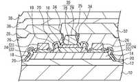
半導体装置100は、絶縁膜18、絶縁膜20、絶縁膜26、絶縁膜35、絶縁膜36、絶縁膜38、2つのベース電極24、エミッタ電極30、および配線32(第2電極)を有し、不図示のコレクタ電極も有する。ベース電極24は、オーミック電極22および上部電極23を有する。エミッタ電極30は、オーミック電極28および上部電極29(第1電極)を有する。 The
絶縁膜18は、ベース層14の上面のうち周縁部と、ベース層14の側面とを連続的に覆う。絶縁膜18は、エミッタ層16の上面のうち周縁部と、エミッタ層16の側面とを連続的に覆う。絶縁膜18は、ベース層14の上に2つの開口部を有し、エミッタ層16の上に1つの開口部を有する。 The insulating
ベース層14のうち、絶縁膜18の開口部から露出する部分に、オーミック電極22が設けられている。エミッタ層16のうち、絶縁膜18の開口部から露出する部分に、エミッタ電極30が設けられている。 An
絶縁膜20は、コレクタ層12、ベース層14、エミッタ層16および絶縁膜18の上を覆う。絶縁膜20は、2つのベース電極24のオーミック電極22の上に開口部を有する。 Insulating
上部電極23は、絶縁膜20の開口部から露出するオーミック電極22の表面に設けられ、オーミック電極22に電気的に接続される。オーミック電極22および上部電極23が、ベース電極24を形成する。2つのベース電極24は、不図示の配線などで互いに電気的に接続される。 The
絶縁膜26は、コレクタ層12、ベース層14、エミッタ層16、絶縁膜18および20、2つのベース電極24を覆う。絶縁膜20および絶縁膜26は、エミッタ電極30のオーミック電極28の上に開口部25を有する。上部電極29は、開口部25から露出するオーミック電極28の表面に設けられ、オーミック電極28に電気的に接続される。上部電極29の断面形状は、例えばテーパ形状である。上部電極29の幅は、図1の下から上に向けて小さくなる。 An insulating
開口部25の断面形状は、上に向けて広がるようなテーパ形状である。開口部25の幅は、図1の下から上に向けて大きくなる。開口部25の内壁は、エミッタ電極30の上部電極29から離間し、上部電極29に対向する。開口部25の内壁には金属層34が設けられている。金属層34は、開口部25の内壁の全体を覆う。金属層34の下端は、エミッタ電極30の上部電極29に接触する。金属層34の上端は、開口部25の上端まで到達する。配線32は、上部電極29の上面および側面に接触し、金属層34に接触する。配線32は、開口部25の内側から絶縁膜26の上まで延伸する、引き出し配線である。 The cross-sectional shape of the
絶縁膜26の上に絶縁膜35が設けられている。絶縁膜26、絶縁膜35および配線32の上に絶縁膜36が設けられている。絶縁膜36の上に絶縁膜38が設けられている。 An insulating
絶縁膜18および20は、例えば窒化シリコン(SiN)で形成されている。絶縁膜18のうち最も厚い部分の厚さは、例えば250nmである。絶縁膜20のうち最も厚い部分の厚さは、例えば100nmである。絶縁膜26は、例えば酸窒化シリコン(SiON)で形成されている。絶縁膜26のうち最も厚い部分の厚さは、例えば650nmである。絶縁膜26は、コレクタ層12の上、およびメサ状のエミッタ層16の上を覆う程度の厚さを有する。絶縁膜35、36および38は、例えばSiONで形成されている。 The insulating
ベース電極24のオーミック電極22、およびエミッタ電極30のオーミック電極28は、それぞれ第1の白金(Pt)層、チタン(Ti)層、第2のPt層、および金(Au)層を含む。第1のPt層、Ti層、第2のPt層、およびAu層は、例えば図1の下側から上側に向けて、この順に積層されている。第1のPt層の厚さは、例えば15nmである。Ti層の厚さは、例えば20nmである。第2のPt層の厚さは、例えば20nmである。Au層の厚さは、例えば100nmである。
ベース電極24の上部電極23は、例えばAuなどの金属で形成されている。エミッタ電極30の上部電極29は、例えば厚さ550nmのAuで形成されている。配線32は、例えばTi層、Pt層およびAu層を含む。Ti層、Pt層およびAu層は、この順に積層されている。Ti層の厚さは、例えば50nmである。Pt層の厚さは、例えば50nmである。Au層の厚さは、例えば570nmである。金属層34は、エミッタ電極30の上部電極29と同じ材料で形成され、例えばAuで形成されている。金属層34の厚さは、例えば2nm以上である。 The
(製造方法)
図2Aから図7Bは、半導体装置100の製造方法を例示する断面図である。図2Aに示すように、例えば有機金属気相成長法(MOCVD:Metal Organic Chemical Vapor Deposition)などで、基板10の上面に、コレクタ層12、ベース層14、およびエミッタ層16をエピタキシャル成長する。エッチングなどで、ベース層14およびエミッタ層16にメサ構造を形成する。真空蒸着およびリフトオフなどにより、ベース層14の上面に2つのオーミック電極22を形成する。エミッタ層16の上面にオーミック電極28を形成する。図2Bに示すように、例えばプラズマCVD法などにより、絶縁膜18および20を形成する。(Production method)
2A to 7B are cross-sectional views illustrating the method for manufacturing the
図2Cに示すように、絶縁膜20のうちオーミック電極22の上の部分に、開口部を形成する。メッキ処理などを行い、オーミック電極22の上面に上部電極23を形成する。例えばプラズマCVD法などにより、絶縁膜26を形成する。 As shown in FIG. 2C, an opening is formed in a portion of the insulating
図3Aに示すように、絶縁膜26の上面にレジスト40(第2レジスト)を塗布する。フォトリソグラフィ法により、レジスト40に開口部40aを形成する。開口部40aは、オーミック電極28の上に位置する。開口部40aからは、絶縁膜26の一部が露出する。 As shown in FIG. 3A, the upper surface of the insulating
図3Bに示すように、レジスト40をマスクとして、絶縁膜26および20のうちオーミック電極28上の部分をエッチングすることで、絶縁膜26に開口部25を形成する。エッチングは、例えばドライエッチングであり、一例としては四フッ化メタン(CF4)のプラズマなどを用いた反応性イオンエッチング(RIE:Reactive Ion Etching)である。絶縁膜26および20は、絶縁膜26の厚さ方向(図の上下方向)にエッチングされるとともに、横方向にもエッチングされる。このサイドエッチングにより、開口部25の幅は、レジスト40の開口部40aの幅より大きくなる。レジスト40は、開口部25の内壁よりもせり出し、庇状になる。開口部25は、上に向けて末広がりのテーパ形状となる。開口部25からはオーミック電極28が露出する。As shown in FIG. 3B, the
図4Aに示すように、真空蒸着およびリフトオフにより、上部電極29を形成する。真空蒸着においてAuは、図4Aの上方向から下方向に向けて導入される。Auがレジスト40の上に堆積することで、レジスト40の上に金属層41が形成される。Auがオーミック電極28の上に堆積することで、オーミック電極28の上に上部電極29が形成される。レジスト40は、開口部25よりもせり出しているため、開口部25のうちレジスト40の下の部分にはAuが堆積しにくい。Auは、開口部25の中央側で厚く堆積し、周縁側で薄く堆積する。この結果、上部電極29はテーパ形状となる。開口部25の内壁の上にはレジスト40が位置するため、内壁にはAuが付着しにくい。開口部25の内壁は露出し、上部電極29から離間する。開口部25の内壁は、例えば深さ400nm以上、500nm以下にわたって露出する。図4Bに示すように、金属層41とともにレジスト40を除去する。オーミック電極28の上に、Auの上部電極29が残る。 As shown in FIG. 4A, the
図5Aに矢印で示すように、絶縁膜26および上部電極29に上側からO2プラズマを照射することで、酸素アッシング(O2アッシング)を行う。O2アッシングの条件は、例えば以下のものとする。
パワー:660W
圧力:1torr(133.32Pa)
時間:30分
O2アッシングは、上部電極29に対してスパッタリング効果を有する処理である。O2アッシングにより、上部電極29を構成する金属(Au)が周囲に飛び散り、開口部25の内壁に堆積する。Auが堆積することで、開口部25の内壁に金属層34が形成される。O2アッシングの条件を上記のものとすることで、金属層34の厚さは例えば2nm以上となる。金属層34の下端は、上部電極29に接触している。金属層34の上端は、絶縁膜26の上端と同じ高さに位置する。絶縁膜26は、O2アッシングによってエッチングされない。As indicated by arrows in FIG. 5A, oxygen ashing (O2 ashing) is performed by irradiating the insulating
Power: 660W
Pressure: 1 torr (133.32 Pa)
Time: 30 minutes O2 ashing is a process that has a sputtering effect on the
図5Bに示すように、絶縁膜26の上にレジスト42(第1レジスト)を形成する。フォトリソグラフィ法などでレジスト42にパターンを形成する。絶縁膜26の上面の一部はレジスト42に覆われる。絶縁膜26の上面の別の一部、開口部25、上部電極29は、レジスト42から露出する。レジスト42の残存物が上部電極29の表面に付着していることがある。そこでレジスト42の形成の後、イソプロピルアルコール(IPA:Isopropyl Alcohol)などで洗浄する。さらに、図6Aに示すようにO2アッシングを行い、残存物を取り除く。O2アッシングの条件は、例えば以下のものとする。
パワー:660W
圧力:1torr(133.32Pa)
時間:3分As shown in FIG. 5B, a resist 42 (first resist) is formed on the insulating
Power: 660W
Pressure: 1 torr (133.32 Pa)
Time: 3 minutes
金属層34を形成するためのO2アッシング、およびレジスト残存物を除去するためのO2アッシングにより、上部電極29の表面に酸化膜が形成される。図6Bに示すように、例えばドライエッチングを行うことで、表面から酸化膜を除去する。ドライエッチングは、例えば六フッ化硫黄(SF6)または四フッ化メタン(CF4)を用いたプラズマエッチングである。条件の例を以下に記載する。
SF6を使用する際の条件
流量:25sccm
圧力:600mTorr(80Pa)
パワー:50W
時間:30秒
CF4を使用する際の条件
流量:45sccm
圧力:625mTorr(83Pa)
パワー:35W
時間:35秒An oxide film is formed on the surface of
Condition flow rate when using SF6:25sccm
Pressure: 600mTorr (80Pa)
Power: 50W
Time: 30 seconds Conditions when using CF4 Flow rate:45 sccm
Pressure: 625mTorr (83Pa)
Power: 35W
Time: 35 seconds
SiONの絶縁膜26の表面は、ドライエッチングによってエッチングされる。しかし、開口部25の内壁は、金属層34で覆われている。したがって内壁のエッチングは抑制される。金属層34で内壁を保護することで、開口部25が横方向および縦方向に拡大することが抑制される。開口部25が深くなることが抑制され、エミッタ層16が露出しない。 The surface of the
図7Aおよび図7Bに示すように、真空蒸着およびリフトオフにより、配線32を形成する。Ti、PtおよびAuをこの順番で、上部電極29、絶縁膜26、金属層34、およびレジスト42の上に堆積する。図7Aに示すように、上部電極29および絶縁膜26の上に配線32が形成される。配線32は、絶縁膜26の開口部25の内側から、絶縁膜26の上面まで延伸する。配線32は、上部電極29および金属層34に接触する。真空蒸着により、レジスト42の上に金属層44が形成される。レジスト42を、金属層44とともに除去する。図7Bに示すように、配線32は残存する。例えばプラズマCVD法などにより、絶縁膜26の上に絶縁膜35を形成する。絶縁膜35および配線32の上に絶縁膜36を形成する。絶縁膜36の上に絶縁膜38を形成する。以上の工程で半導体装置100が形成される。 As shown in FIGS. 7A and 7B, wiring 32 is formed by vacuum deposition and lift-off. Ti, Pt and Au are deposited in this order on the
上部電極29と金属層34とは、同じ材料(例えばAu)で形成されている。上部電極29は真空蒸着で製造される。金属層34はスパッタリングで製造される。製造の手法が異なるため、上部電極29の結晶性と、金属層34の結晶性とは異なる。上部電極29および金属層34それぞれに、電子線回折を行い、干渉パターンを比較する。上部電極29および金属層34それぞれから、厚さ約100±20nmのサンプルを取得し、サンプルに電子線を照射する。 The
図8Aは、上部電極29の回折パターンを例示する模式図である。図8Bは、金属層34の回折パターンを例示する模式図である。図8Aに示す上部電極29の回折パターンは、図8Bに示す金属層34の回折パターンに比べて、規則性が高い。図8Bに示す金属層34の回折パターンは、リング状である。真空蒸着において、Auの原子が規則的に堆積する。このため、上部電極29は、金属層34に比べて単結晶に近くなる。一方、スパッタリング効果ではじき出されたAuの粒子は、ランダムに堆積する。金属層34は、上部電極29に比べて、より不規則な組織を有する。 FIG. 8A is a schematic diagram illustrating the diffraction pattern of the
(比較例)
図9Aから図10は、比較例における製造方法を例示する断面図である。図9Aに示すように、比較例では、金属層34を形成しない。つまり、絶縁膜26に開口部25を設けた後、O2アッシングを行わず、レジスト42を形成する。(Comparative example)
9A to 10 are cross-sectional views illustrating the manufacturing method in the comparative example. As shown in FIG. 9A, the
レジスト42の残存物を除去するために、O2アッシングを行う。O2アッシングによって上部電極29に酸化膜が形成される。上部電極29の酸化膜を取り除くため、ドライエッチングを行う。絶縁膜26および絶縁膜20もドライエッチングされる。図9Bに示すように、ドライエッチングは、開口部25の内壁、開口部25の下の絶縁膜18および20にも進む。開口部25が、エミッタ層16に到達するまで深くなる。開口部25の内壁と上部電極29との間に隙間が生じ、隙間からオーミック電極28およびエミッタ層16が露出する。図10に示すように、配線32を形成すると、配線32がエミッタ層16に接触する。配線32の材料である金属(Au)が、エミッタ層16に拡散する。金属の拡散によって、例えば電流増幅率などの特性が変動してしまう。O2 ashing is performed to remove remnants of resist 42 . An oxide film is formed on the
本実施形態によれば、絶縁膜26の開口部25の内側に上部電極29を形成した後、上部電極29にO2アッシングを行う。O2アッシングは、上部電極29に対してスパッタリング効果を有する。図5Aに示すように、上部電極29の金属(例えばAu)が飛散し、開口部25の内壁に付着し、金属層34が形成される。開口部25の内壁は金属層34で覆われるため、エッチングされにくい。金属層34の形成後に、例えばフッ素系ガスを用いたドライエッチングを行っても、開口部25の内壁のエッチングは抑制される。開口部25の内壁と、上部電極29との間に隙間が発生しにくい。エッチングが絶縁膜18および20に進むことも抑制される。エミッタ層16などの半導体層が、開口部25から露出しない。図1に示すように、配線32がエミッタ層16などの半導体層に接触することが抑制される。配線32の金属がエミッタ層16などの半導体層に拡散しにくく、金属の拡散による性能の変化が抑制される。したがって、半導体装置100の信頼性の低下が抑制される。According to this embodiment, after forming the
比較例と実施形態とに対して、210℃の環境下で10分間の通電試験を行った。比較例における電流増幅率の変動幅は、10%以上だった。実施形態における電流増幅率の変動幅は、-6%程度だった。実施例によれば、性能の変化が抑制され、半導体装置100の動作を継続しても高い信頼性が得られる。 A 10-minute energization test was performed in a 210° C. environment for the comparative example and the embodiment. The fluctuation width of the current amplification factor in the comparative example was 10% or more. The fluctuation width of the current amplification factor in the embodiment was about -6%. According to the embodiment, changes in performance are suppressed, and high reliability can be obtained even if the operation of the
O2アッシングを上部電極29に行うことで、上部電極29の金属が周囲に飛散し、金属層34を形成する。O2アッシング以外に例えばドライエッチングなど、上部電極29にスパッタリング効果を有する処理を行うことで、金属層34を形成することもできる。ドライエッチングに比べ、O2アッシングは、絶縁膜26にダメージを与えにくく、かつ上部電極29にスパッタリング効果を有する。ドライエッチングもスパッタリング効果を有する。しかし、O2アッシングは、ドライエッチングに比べて、基板10を装置内にセットしてからアッシング処理までの処理時間を短時間にすることができる。工程の効率化のため、O2アッシングを行うことが好ましい。By performing O2 ashing on the
金属層34が薄いと、金属層34に欠陥が生じ、開口部25の内壁が露出する恐れがある。開口部25の内壁を保護するため、金属層34の厚さは例えば2μm以上であることが好ましい。O2アッシングを例えば30分以上行うことで、厚さ2μm以上の金属層34を形成することができる。O2アッシングの時間を長くすることで、金属層34をより厚くすることができる。ただし、O2アッシングの時間が長くなることで工数が増大してしまう。例えば、金属層34の厚さは3μm以下であることが好ましい。金属層34の厚さが2μm以上、3μm以下ならば、内壁を十分に保護することができ、かつ工数の増大を抑制することができる。If the
図4Aに示すように、上部電極29は、レジスト40を用いた真空蒸着およびリフトオフにより形成される。レジスト40の残存物を上部電極29の表面から取り除くため、図6AのO2アッシングを行う。O2アッシングにより、上部電極29の表面には酸化膜が形成される。図6Bに示すように、例えばフッ素系ガスを用いたドライエッチングにより、酸化膜を取り除く。酸化膜を取り除いた上部電極29の表面に、図7Aに示す配線32を形成することで、上部電極29と配線32との間の接触抵抗を低減することができる。As shown in FIG. 4A,
上部電極29表面の酸化膜を取り除くために、フッ素系ガスを用いたドライエッチングを行う。フッ素系ガスを用いたドライエッチングは、絶縁膜26、20および18にエッチング効果を有する処理である。開口部25の内壁に金属層34が形成されているため、開口部25の内壁のエッチングが抑制される。ドライエッチングは、フッ素系ガス以外を用いたエッチングでもよい。酸化膜を取り除く処理は、ドライエッチング以外に、例えばフッ酸などの薬品を用いたウェットエッチングでもよい。絶縁膜26は、SiONで形成されてもよいし、SiNなど他の絶縁体で形成されてもよい。絶縁膜18および20は、SiNで形成されてもよいし、SiONで形成されてもよい。 In order to remove the oxide film on the surface of the
図3Bに示すように、レジスト40を用いて絶縁膜26および20をエッチングすることで、開口部25が形成される。レジスト40は庇状になる。図4Aに示すように、上部電極29は、レジスト40を用いた真空蒸着およびリフトオフにより形成される。レジスト40の下に金属が堆積しないため、上部電極29がテーパ形状となる。開口部25の内壁は、上部電極29から離間し、例えば深さ400nm以上、500nm以下にわたって露出する。比較例においては、露出する内壁がエッチングされる。実施形態では、金属層34が内壁を覆う。したがって、内壁のエッチングが抑制される。 As shown in FIG. 3B,
上部電極29は、Auで形成されている。上部電極29にO2アッシングを行うと、O2アッシングのスパッタリング効果によって、上部電極29の表面からAuが飛散し、Auから金属層34が形成される。配線32は、例えばTi、PtおよびAuを順に積層したものである。上部電極29および金属層34のAuの表面に、配線32が接触することで、電気的な接続の信頼性が向上する。上部電極29、金属層34、および配線32は、上記のもの以外の金属で形成されてもよい。The
ベース層14およびエミッタ層16は、それぞれメサ状であり、基板10の上面から突出する。絶縁膜26は、メサ状のベース層14およびエミッタ層16を覆う。配線32は、絶縁膜26の開口部25から絶縁膜26の上面まで延伸する。配線32を上部電極29から引き出すため、絶縁膜26および20に開口部25を形成する。開口部25の内壁を金属層34で覆うことで、開口部25の内壁のエッチングが抑制され、配線32とエミッタ層16との接触が抑制される。エミッタ電極30以外の電極に実施形態を適用してもよい。半導体装置100はHBTとしたが、HBT以外の装置でもよい。 The
以上、本開示の実施形態について詳述したが、本開示は係る特定の実施形態に限定されるものではなく、特許請求の範囲に記載された本開示の要旨の範囲内において、種々の変形・変更が可能である。 Although the embodiments of the present disclosure have been described in detail above, the present disclosure is not limited to such specific embodiments, and various modifications and variations can be made within the scope of the gist of the present disclosure described in the claims. Change is possible.
10 基板
12 コレクタ層
14 ベース層
16 エミッタ層
18、20、26、35、36、38 絶縁膜
22、28 オーミック電極
23、29 上部電極
25、40a 開口部
32 配線
34、41、44 金属層
40、42 レジスト
100 半導体装置
REFERENCE SIGNS
Claims (9)
Translated fromJapanese前記絶縁膜に開口部を形成する工程と、
前記開口部の内側に、前記半導体層に電気的に接続される第1電極を形成する工程と、
前記第1電極にスパッタリング効果を有する処理を前記第1電極に行うことで、前記開口部の内壁に金属層を形成する工程と、
前記金属層を形成する工程の後、前記絶縁膜に対してエッチング効果を有する処理を、前記第1電極および前記絶縁膜の表面を含む領域に実施する工程と、を有する半導体装置の製造方法。forming an insulating film on the upper surface of the semiconductor layer;
forming an opening in the insulating film;
forming a first electrode electrically connected to the semiconductor layer inside the opening;
forming a metal layer on the inner wall of the opening by subjecting the first electrode to a process having a sputtering effect on the first electrode;
A method of manufacturing a semiconductor device, comprising, after forming the metal layer, subjecting a region including the surface of the first electrode and the insulating film to a process having an etching effect on the insulating film.
前記第1レジストを形成する工程の後に、前記第1電極に酸素アッシングを行う工程と、
前記第1レジストを用い、真空蒸着およびリフトオフにより第2電極を形成する工程と、をさらに有し、
前記エッチング効果を有する処理は、前記第1電極に酸素アッシングを行う工程の後に実施される請求項1から請求項4のいずれか一項に記載の半導体装置の製造方法。a step of forming a first resist on the insulating film after the step of forming the metal layer and before the step of performing the treatment having an etching effect;
a step of performing oxygen ashing on the first electrode after the step of forming the first resist;
forming a second electrode by vacuum deposition and lift-off using the first resist;
5. The method of manufacturing a semiconductor device according to claim 1, wherein the treatment having an etching effect is performed after the step of oxygen ashing the first electrode.
前記開口部を形成する工程は、前記第2レジストを用いて前記絶縁膜をエッチングすることで前記開口部を形成する工程であり、
前記第1電極を形成する工程は、前記第2レジストを用い、真空蒸着およびリフトオフにより前記第1電極を形成する工程である請求項1から請求項6のいずれか一項に記載の半導体装置の製造方法。forming a second resist on the insulating film;
The step of forming the opening is a step of forming the opening by etching the insulating film using the second resist,
7. The semiconductor device according to claim 1, wherein the step of forming the first electrode is a step of forming the first electrode by vacuum deposition and lift-off using the second resist. Production method.
前記金属層を形成する工程は、前記スパッタリング効果を有する処理を前記第1電極に行うことで、前記第1金属の表面の前記金から前記金属層を形成する工程である請求項1から請求項8のいずれか一項に記載の半導体装置の製造方法。
The step of forming the first electrode is a step of forming the first electrode having a gold surface,
The step of forming the metal layer is a step of forming the metal layer from the gold on the surface of the first metal by subjecting the first electrode to a process having the sputtering effect. 9. The method for manufacturing a semiconductor device according to any one of 8.
Priority Applications (1)
| Application Number | Priority Date | Filing Date | Title |
|---|---|---|---|
| JP2021094323AJP7685373B2 (en) | 2021-06-04 | 2021-06-04 | Semiconductor device manufacturing method |
Applications Claiming Priority (1)
| Application Number | Priority Date | Filing Date | Title |
|---|---|---|---|
| JP2021094323AJP7685373B2 (en) | 2021-06-04 | 2021-06-04 | Semiconductor device manufacturing method |
Publications (2)
| Publication Number | Publication Date |
|---|---|
| JP2022186213Atrue JP2022186213A (en) | 2022-12-15 |
| JP7685373B2 JP7685373B2 (en) | 2025-05-29 |
Family
ID=84441643
Family Applications (1)
| Application Number | Title | Priority Date | Filing Date |
|---|---|---|---|
| JP2021094323AActiveJP7685373B2 (en) | 2021-06-04 | 2021-06-04 | Semiconductor device manufacturing method |
Country Status (1)
| Country | Link |
|---|---|
| JP (1) | JP7685373B2 (en) |
Citations (4)
| Publication number | Priority date | Publication date | Assignee | Title |
|---|---|---|---|---|
| JP2003152077A (en)* | 2001-11-15 | 2003-05-23 | Hitachi Ltd | Semiconductor device and method of manufacturing semiconductor device |
| JP2003257973A (en)* | 2002-03-04 | 2003-09-12 | Sumitomo Electric Ind Ltd | Via hole formation method |
| JP2011082254A (en)* | 2009-10-05 | 2011-04-21 | Sumitomo Electric Ind Ltd | Method for manufacturing semiconductor device |
| JP2015032631A (en)* | 2013-07-31 | 2015-02-16 | 住友電気工業株式会社 | Semiconductor device, and method of manufacturing the same |
- 2021
- 2021-06-04JPJP2021094323Apatent/JP7685373B2/enactiveActive
Patent Citations (4)
| Publication number | Priority date | Publication date | Assignee | Title |
|---|---|---|---|---|
| JP2003152077A (en)* | 2001-11-15 | 2003-05-23 | Hitachi Ltd | Semiconductor device and method of manufacturing semiconductor device |
| JP2003257973A (en)* | 2002-03-04 | 2003-09-12 | Sumitomo Electric Ind Ltd | Via hole formation method |
| JP2011082254A (en)* | 2009-10-05 | 2011-04-21 | Sumitomo Electric Ind Ltd | Method for manufacturing semiconductor device |
| JP2015032631A (en)* | 2013-07-31 | 2015-02-16 | 住友電気工業株式会社 | Semiconductor device, and method of manufacturing the same |
Also Published As
| Publication number | Publication date |
|---|---|
| JP7685373B2 (en) | 2025-05-29 |
Similar Documents
| Publication | Publication Date | Title |
|---|---|---|
| US6368929B1 (en) | Method of manufacturing a semiconductor component and semiconductor component thereof | |
| JPH07335674A (en) | III-V semiconductor gate structure and method of manufacturing the same | |
| US20220020642A1 (en) | Ald (atomic layer deposition) liner for via profile control and related applications | |
| US7585779B2 (en) | Fabrication method of semiconductor device | |
| CN111312808B (en) | Semiconductor device and manufacturing method thereof | |
| CN116544113A (en) | Manufacturing process of ohmic contact piece of HEMT device and HEMT device | |
| JP3502651B2 (en) | Electrode formation method | |
| CN1136605C (en) | Method for making semi-conductor device | |
| US12211699B2 (en) | Method of removing step height on gate structure | |
| US20050258459A1 (en) | Method for fabricating semiconductor devices having a substrate which includes group III-nitride material | |
| US8043965B2 (en) | Method of forming a through substrate via in a compound semiconductor | |
| JP3621752B2 (en) | Method for manufacturing III-V semiconductor gate structure | |
| JP7685373B2 (en) | Semiconductor device manufacturing method | |
| US20240266184A1 (en) | Method of manufacturing semiconductor structure | |
| TW202332051A (en) | Hemt and method of fabricating the same | |
| CN117995877A (en) | Transistor structure and method for manufacturing the same | |
| JP2879841B2 (en) | Manufacturing method of planar diode | |
| US11121229B2 (en) | Methods of fabricating semiconductor structures and high electron mobility transistors | |
| KR100680944B1 (en) | Manufacturing method of semiconductor device | |
| CN115036218B (en) | Method for preparing copper interconnect structure | |
| TW202447716A (en) | Semiconductor structure and manufacturing method thereof | |
| CN118448457A (en) | Vertical semiconductor component based on gallium nitride with a structured intermediate layer | |
| JP3627705B2 (en) | Electrode formation method | |
| KR102008460B1 (en) | Method of Manufacturing of Super Self-Alignment Bipolar Transistor | |
| CN1436367A (en) | Method for mfg. semiconductor device and semiconductor device thereby |
Legal Events
| Date | Code | Title | Description |
|---|---|---|---|
| A621 | Written request for application examination | Free format text:JAPANESE INTERMEDIATE CODE: A621 Effective date:20240122 | |
| A977 | Report on retrieval | Free format text:JAPANESE INTERMEDIATE CODE: A971007 Effective date:20241018 | |
| A131 | Notification of reasons for refusal | Free format text:JAPANESE INTERMEDIATE CODE: A131 Effective date:20241022 | |
| A601 | Written request for extension of time | Free format text:JAPANESE INTERMEDIATE CODE: A601 Effective date:20241220 | |
| RD02 | Notification of acceptance of power of attorney | Free format text:JAPANESE INTERMEDIATE CODE: A7422 Effective date:20241220 | |
| RD04 | Notification of resignation of power of attorney | Free format text:JAPANESE INTERMEDIATE CODE: A7424 Effective date:20241220 | |
| A521 | Request for written amendment filed | Free format text:JAPANESE INTERMEDIATE CODE: A523 Effective date:20250219 | |
| TRDD | Decision of grant or rejection written | ||
| A01 | Written decision to grant a patent or to grant a registration (utility model) | Free format text:JAPANESE INTERMEDIATE CODE: A01 Effective date:20250430 | |
| A61 | First payment of annual fees (during grant procedure) | Free format text:JAPANESE INTERMEDIATE CODE: A61 Effective date:20250519 | |
| R150 | Certificate of patent or registration of utility model | Ref document number:7685373 Country of ref document:JP Free format text:JAPANESE INTERMEDIATE CODE: R150 |