JP2022179625A - semiconductor equipment - Google Patents
semiconductor equipmentDownload PDFInfo
- Publication number
- JP2022179625A JP2022179625AJP2022162033AJP2022162033AJP2022179625AJP 2022179625 AJP2022179625 AJP 2022179625AJP 2022162033 AJP2022162033 AJP 2022162033AJP 2022162033 AJP2022162033 AJP 2022162033AJP 2022179625 AJP2022179625 AJP 2022179625A
- Authority
- JP
- Japan
- Prior art keywords
- substrate
- layer
- wiring layer
- nonvolatile semiconductor
- semiconductor memory
- Prior art date
- Legal status (The legal status is an assumption and is not a legal conclusion. Google has not performed a legal analysis and makes no representation as to the accuracy of the status listed.)
- Granted
Links
Images


Landscapes
- Production Of Multi-Layered Print Wiring Board (AREA)
- Structure Of Printed Boards (AREA)
Abstract
Translated fromJapaneseDescription
Translated fromJapanese本発明は、半導体装置に関する。 The present invention relates to semiconductor devices.
従来、コネクタが形成された基板上に、NANDフラッシュメモリなどの不揮発性半導体記憶素子が搭載された半導体装置が用いられている。また、半導体装置には、不揮発性半導体記憶素子の他に、揮発性半導体記憶素子や、不揮発性半導体記憶素子および揮発性半導体素子を制御するコントローラが搭載される。 2. Description of the Related Art Conventionally, a semiconductor device has been used in which a nonvolatile semiconductor memory element such as a NAND flash memory is mounted on a substrate on which a connector is formed. In addition to the nonvolatile semiconductor memory elements, the semiconductor device also includes a volatile semiconductor memory element and a controller that controls the nonvolatile semiconductor memory element and the volatile semiconductor element.
このような半導体装置は、その使用環境や規格などに合わせて、基板の形状や大きさが制約される場合があり、例えば、平面視において長方形形状を呈する基板を用いる場合がある。また、近年の半導体装置への小型化の要求により、基板が薄型化する傾向にある。このような、薄型化された長方形形状の基板を用いる場合に、基板の反りを抑えることが求められている。 In such a semiconductor device, there are cases where the shape and size of the substrate are restricted according to the usage environment and standards. In addition, due to the recent demand for miniaturization of semiconductor devices, substrates tend to be thinner. When such a thin rectangular substrate is used, it is required to suppress warping of the substrate.
本発明は、基板の反りを抑えることができる半導体装置を提供することを目的とする。 An object of the present invention is to provide a semiconductor device capable of suppressing warping of a substrate.
実施形態に係る半導体装置は、基板と、第1から第3の不揮発性半導体メモリと、揮発性半導体メモリと、を備える。前記基板は、第1の主面と、前記第1の主面とは反対側を向いた第2の主面を有する。前記第1から第3の不揮発性半導体メモリは、前記基板の前記第1の主面に搭載されている。前記揮発性半導体メモリは、前記基板の前記第1の主面に搭載されている。前記基板は、前記第1の主面に設けられる第1の配線層と、前記第2の主面に設けられた網状配線層としての第2の配線層と、内層として形成される複数の配線層と、これら配線層間にそれぞれ設けられる複数の絶縁層と、を備える。前記内層として形成される複数の前記配線層のうち第3から第5の配線層はプレーン層である。前記第3の配線層は、前記基板の層構造の中心線よりも前記第1の主面側に形成され、絶縁層を隔てて前記第1の配線層と対向する。前記第4の配線層及び前記第5の配線層は、前記基板の層構造の中心線よりも前記第2の主面側に形成される。前記第5の配線層は絶縁層を隔てて前記第2の配線層と対向する。前記第5の配線層において、前記第1の不揮発性半導体メモリと前記第2の不揮発性半導体メモリの隙間に対向する部分の一部に第1のスリットが形成され、前記第2の不揮発性半導体メモリと前記第3の不揮発性半導体メモリの隙間に対向する部分の一部に第2のスリットが形成される。前記内層として形成される複数の前記配線層のうち信号を送受信するための信号層である第6の配線層が、前記第4の配線層及び前記第5の配線層と絶縁層を隔ててそれぞれ対向する。前記内層として形成される複数の配線層のうち絶縁層を隔てて前記第3の配線層と対向する第7の配線層及び前記第1の配線層は、信号を送受信するための信号層である。前記第1の配線層の表面は、ソルダーレジストに覆われている。 A semiconductor device according to an embodiment includes a substrate, first to third nonvolatile semiconductor memories, and a volatile semiconductor memory. The substrate has a first main surface and a second main surface facing away from the first main surface. The first to third nonvolatile semiconductor memories are mounted on the first main surface of the substrate. The volatile semiconductor memory is mounted on the first main surface of the substrate. The substrate includes a first wiring layer provided on the first main surface, a second wiring layer as a mesh wiring layer provided on the second main surface, and a plurality of wirings formed as inner layers. and a plurality of insulating layers respectively provided between these wiring layers. Of the plurality of wiring layers formed as the inner layers, the third to fifth wiring layers are plane layers. The third wiring layer is formed closer to the first main surface than the center line of the layered structure of the substrate, and faces the first wiring layer with an insulating layer therebetween. The fourth wiring layer and the fifth wiring layer are formed closer to the second main surface than the center line of the layered structure of the substrate. The fifth wiring layer faces the second wiring layer with an insulating layer interposed therebetween. A first slit is formed in a portion of the fifth wiring layer facing a gap between the first nonvolatile semiconductor memory and the second nonvolatile semiconductor memory, and the second nonvolatile semiconductor memory is provided with a first slit. A second slit is formed in a portion of the portion facing the gap between the memory and the third nonvolatile semiconductor memory. Of the plurality of wiring layers formed as the inner layers, a sixth wiring layer, which is a signal layer for transmitting and receiving signals, is separated from the fourth wiring layer and the fifth wiring layer by an insulating layer. opposite. Of the plurality of wiring layers formed as the inner layers, the seventh wiring layer and the first wiring layer facing the third wiring layer across an insulating layer are signal layers for transmitting and receiving signals. . A surface of the first wiring layer is covered with a solder resist.
以下に添付図面を参照して、本発明の実施の形態にかかる半導体装置を詳細に説明する。なお、これらの実施の形態により本発明が限定されるものではない。 Semiconductor devices according to embodiments of the present invention will be described in detail below with reference to the accompanying drawings. It should be noted that the present invention is not limited by these embodiments.
(第1の実施の形態)
図1は、第1の実施の形態にかかる半導体装置の構成例を示すブロック図である。半導体装置100は、SATAインタフェース(ATA I/F)2などのメモリ接続インタフェースを介してパーソナルコンピュータあるいはCPUコアなどのホスト装置(以下、ホストと略す)1と接続され、ホスト1の外部メモリとして機能する。ホスト1としては、パーソナルコンピュータのCPU、スチルカメラ、ビデオカメラなどの撮像装置のCPUなどがあげられる。また、半導体装置100は、RS232Cインタフェース(RS232C I/F)などの通信インタフェース3を介して、デバッグ用機器200との間でデータを送受信することができる。(First embodiment)
FIG. 1 is a block diagram of a configuration example of a semiconductor device according to a first embodiment. A
半導体装置100は、不揮発性半導体記憶素子としてのNAND型フラッシュメモリ(以下、NANDメモリと略す)10と、コントローラとしてのドライブ制御回路4と、NANDメモリ10よりも高速記憶動作が可能な揮発性半導体記憶素子であるDRAM20と、電源回路5と、状態表示用のLED6と、ドライブ内部の温度を検出する温度センサ7とを備えている。温度センサ7は、例えばNANDメモリ10の温度を直接または間接的に測定する。ドライブ制御回路4は、温度センサ7による測定結果が一定温度以上となった場合に、NANDメモリ10への情報の書き込みなどを制限して、それ以上の温度上昇を抑制する。 The
電源回路5は、ホスト1側の電源回路から供給される外部直流電源から複数の異なる内部直流電源電圧を生成し、これら内部直流電源電圧を半導体装置100内の各回路に供給する。また、電源回路5は、外部電源の立ち上がりを検知し、パワーオンリセット信号を生成して、ドライブ制御回路4に供給する。 The
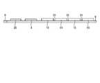
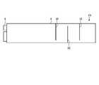
図2は、半導体装置100の概略構成を示す平面図である。図3は、半導体装置100の側面図である。電源回路5、DRAM20、ドライブ制御回路4、NANDメモリ10は、配線パターンが形成された基板8上に搭載される。基板8は、平面視において略長方形形状を呈する。略長方形形状を呈する基板8の一方の短辺側には、ホスト1に接続されて、上述したSATAインタフェース2、通信インタフェース3として機能するコネクタ9が設けられている。コネクタ9は、ホスト1から入力された電源を電源回路5に供給する電源入力部として機能する。コネクタ9は、例えばLIFコネクタである。なお、コネクタ9には、基板8の短手方向に沿った中心位置からずれた位置にスリット9aが形成されており、ホスト1側に設けられた突起(図示せず)などと嵌まり合うようになっている。これにより、半導体装置100が表裏逆に取り付けられることを防ぐことができる。 FIG. 2 is a plan view showing a schematic configuration of the
基板8は、合成樹脂を重ねて形成された多層構造になっており、例えば8層構造となっている。なお、基板8の層数は8層に限られない。図4は、基板8の層構成を示す図である。基板8には、合成樹脂で構成された各層(絶縁膜8a)の表面あるいは内層に様々な形状で配線層8bとして配線パターンが形成されている。配線パターンは、例えば銅で形成される。基板8に形成された配線パターンを介して、基板8上に搭載された電源回路5、DRAM20、ドライブ制御回路4、NANDメモリ10同士が電気的に接続される。また、基板の表面(第1層側)と裏面(第8層側)は、保護膜としてソルダーレジスト8cに覆われている。 The
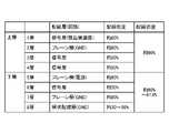
図5は、基板8の各層の配線密度を示す図である。ここで、基板8の層構造の中心線30(図4も参照)よりも表面層側に形成された第1層から第4層までを上層といい、中心線30よりも裏面層側に形成された第5層から第8層までを下層という。 FIG. 5 is a diagram showing the wiring density of each layer of the
基板8の各層に形成された配線層8bは、図5に示すように、信号を送受信する信号層、グランドや電源線となるプレーン層として機能する。そして、各層に形成された配線パターンの配線密度、すなわち、基板8の表面面積に対する配線層が占める割合を、図5に示すように構成している。 As shown in FIG. 5, the
本実施の形態では、グランドとして機能する第8層をプレーン層ではなく網状配線層とすることで、その配線密度を30~60%に抑えている。ここで、基板8の上層全体での配線密度は約60%となっている。そこで、第8層の配線密度を約30%として配線パターンを形成することで、下層全体での配線密度を約60%とすることができ、上層全体の配線密度と下層全体の配線密度とを略等しくすることができる。なお、第8層の配線密度は、約30~60%の範囲で調整することで、上層全体の配線密度と略等しくなるようにすればよい。 In this embodiment, the wiring density is suppressed to 30 to 60% by using a mesh wiring layer instead of a plain layer for the eighth layer functioning as a ground. Here, the wiring density in the entire upper layer of the
図6は、基板8の裏面層(第8層)に形成された配線パターンを示す図である。図6に示すように、基板8の裏面層(第8層)には配線パターンが網状に形成される。このように、基板8の第8層を網状配線層とすることで、プレーン層として形成するよりも配線密度を低く抑えている。 FIG. 6 is a diagram showing a wiring pattern formed on the back surface layer (eighth layer) of the
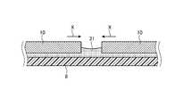
裏面層に形成される配線層には、半導体装置100から漏れて他の装置へ与えるノイズの影響を軽減するシールド層としての機能も求められる。図8は、基板の裏面層(第8層)に形成された配線パターンのライン幅と間隔について説明するための図である。図8に示すように、ライン幅Lが0.3mm、ライン間隔Sが0.9mmとなる網状配線が基板8の第8層に形成される。このように形成された網状配線では、開口幅Wが0.9×√2=1.27mmとなる。 The wiring layer formed on the back surface layer is also required to function as a shield layer that reduces the influence of noise that leaks from the
例えば、3GHzのSATA基本波のような高周波であるノイズに対するシールド効果は、以下のようになる。まず、C=f×λ×√εから、SATA基本波の2次高調波の1/2波長(λ/2)を算出する。ここで、Cは光速であり、3.0×108m/sである。fは2次高調波の周波数であり、6.0×109Hzである。εは比誘電率であり、4.6である。For example, the shield effect against high-frequency noise such as SATA fundamental wave of 3 GHz is as follows. First, the half wavelength (λ/2) of the second harmonic of the SATA fundamental wave is calculated from C=f×λ×√ε. where C is the speed of light, which is 3.0×10⁸ m/s. f is the frequency of the second harmonic and is 6.0×10⁹ Hz. ε is the dielectric constant, which is 4.6.
上記条件によれば、λは23.3mmとなり、1/2波長(λ/2)は11.7mmとなる。すなわち、1/2波長(λ/2)は、開口幅W(1.27mm)の約10倍となる。また、λ/20=1.2mmで開口幅Wと略等しくなるため、シールド効果は約-20dBとなる。 According to the above conditions, λ is 23.3 mm and 1/2 wavelength (λ/2) is 11.7 mm. That is, the half wavelength (λ/2) is approximately ten times the aperture width W (1.27 mm). Also, since λ/20=1.2 mm, which is approximately equal to the opening width W, the shielding effect is approximately −20 dB.
図9は、NANDメモリ10の隙間に充填された接着部を示す図である。図9に示すように、NANDメモリ10と基板8との隙間には、合成樹脂材料で構成された接着部31が充填されて、NANDメモリ10と基板8とを接着させている。また、接着部31は、その一部がNANDメモリ10と基板8との隙間からはみ出している。そのはみ出した部分は、基板8の長手方向に沿って並べられたNANDメモリ10同士の隙間に充填される。したがって、接着部31は、NANDメモリ10同士をその側面で接着させている。なお、接着部31は、NANDメモリ10の高さを超えない程度にはみ出しており、NANDメモリ10の表面は露出している。また、図9では、NANDメモリ10の高さの中間部程度まで接着部31を充填させているが、これより低くてもよく、隣接するNANDメモリ10同士に接着部31が接触していればよい。もちろん、図9に示す高さよりも高くなるようにNANDメモリ10間に接着部31を充填してもよい。 FIG. 9 is a diagram showing adhesive portions filled in the gaps of the
図10は、基板8の第7層に形成されたスリットを示す図である。図10では、基板8を裏面層側から見た状態を示し、第8層を省略して示している。また、表面層側に実装されたNANDメモリ10を破線で示している。基板8の第7層には、配線層としてプレーン層が形成される。図10に示すように、基板8の第7層にはプレーン層として第7層の略全域に配線パターンを形成しつつ、その一部にスリット32(配線層が形成されていない部分)を設けている。スリット32は、第7層の略全域に形成された配線パターンのうち、NANDメモリ10の隙間に対向する部分に設けられている。 FIG. 10 shows slits formed in the seventh layer of the
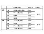
図7は、比較例としての基板の各層の配線密度を示す図である。図7の比較例に示すように、従来の基板では、第8層をプレーン層とすることで、配線密度が約90%となっていた。そのため、下層の配線密度が約75%となり、上層の配線密度(約60%)との差が大きくなっている。配線密度が異なることで、基板8の上層全体に占める絶縁膜8a(合成樹脂)と配線部分(銅)との比率が、基板8の下層全体に占める合成樹脂と銅との比率と異なることとなる。これにより、基板8の上層と下層とで熱膨張係数も異なることとなる。この熱膨張係数の違いにより、基板8の温度変化に伴って、基板8の長手方向に沿って表面層側に凸形状(図3における上に凸形状)となるような反りが発生しやすくなる。このような温度変化は、半導体装置100の製造過程で生じやすい。また、近年の半導体装置への小型化の要求により、基板8も薄型化する傾向にあり、このような反りが発生しやすくなっている。 FIG. 7 is a diagram showing the wiring density of each layer of a substrate as a comparative example. As shown in the comparative example of FIG. 7, in the conventional substrate, the wiring density was about 90% by making the eighth layer a plain layer. Therefore, the wiring density of the lower layer is about 75%, and the difference from the wiring density of the upper layer (about 60%) is large. Due to the different wiring densities, the ratio of the insulating
一方、本実施の形態では、第8層の配線密度は、約30~60%の範囲で調整し、上層全体の配線密度と下層全体の配線密度とを略等しくしているので、熱膨張係数も略等しくなる。そのため、基板8に反りが発生するのを抑制することができる。また、中心線30(図4も参照)から最も離れた第8層で配線密度を調整しているので、反りを抑制するためのモーメントをより大きく発生させることができる。 On the other hand, in the present embodiment, the wiring density of the eighth layer is adjusted in the range of about 30 to 60%, and the wiring density of the entire upper layer and the wiring density of the entire lower layer are substantially equal. are also approximately equal. Therefore, it is possible to prevent the
また、基板8の第8層で配線密度を調整しているので、信号層のように配線レイアウトに制限のある層で配線密度の調整をする場合に比べて、配線設計が容易になり、コストの抑制を図ることができる。 In addition, since the wiring density is adjusted in the eighth layer of the
また、隣接するNANDメモリ10同士の隙間に接着部31が充填されるので、接着部31の結合力により、矢印Xに示すようなNANDメモリ10同士を引き寄せる力が発生する。このNANDメモリ10同士を引き寄せる力は、凸形状となるように基板8を反らせる力に対抗する力となるので、基板8の反りの発生を抑制することができる。 In addition, since the gaps between the
また、基板8の第7層の略全域に形成された配線パターンのうち、NANDメモリ10の隙間に対向する部分に設けられているため、スリット32部分で配線パターンの結合力が弱まる。そのため、NANDメモリ10同士の隙間に接着部31が充填されることによって生じる力(図9の矢印Xも参照)に対抗する力が弱まり、基板8の反りの発生をより一層効果的に抑制することができる。 In addition, among the wiring patterns formed substantially all over the seventh layer of the
なお、本実施の形態では、基板8の下層全体の配線密度を調整するために、第8層の配線層を網状配線層にしているが、これに限られず、例えばライン上に配線層を形成してもよい。また、下層のうち第8層以外の層、すなわち第5層から第7層までの配線層の配線密度を調整して、下層全体としての配線密度を調整してもよい。もちろん、第5層から第8層までのすべての層で配線密度を調整して、下層全体としての配線密度を調整してもよい。 In the present embodiment, the wiring layer of the eighth layer is a mesh wiring layer in order to adjust the wiring density of the entire lower layer of the
また、スリット32が形成される層は第7層に限らない。下層のうち第7層以外の層、すなわち第5層から第6層および第8層にスリットが形成されてもよい。 Also, the layer in which the
(第2の実施の形態)
図11は、第2の実施の形態にかかる半導体装置が備える基板の層構成を示す図である。本実施の形態では、基板8の第8層の外側に、9層目の層として最外層を設けている。そして、最外層の全域を銅箔で覆ってシールド層としている。このように、最外層の全域を銅箔で覆うことで、半導体装置からのノイズの漏れをより確実に防ぐことができる。なお、9層目よりも内側の層の全域を銅箔で覆ってシールド層としてもよい。(Second embodiment)
FIG. 11 is a diagram showing a layer structure of a substrate included in the semiconductor device according to the second embodiment. In this embodiment, the outermost layer is provided as the ninth layer outside the eighth layer of the
(第3の実施の形態)
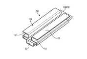
図12は、第3の実施の形態にかかる半導体装置の搬送方法に用いる保持部材の外観斜視図である。図13は、図12に示す保持部材が箱に収納された状態を示す断面図である。本実施の形態では、半導体装置100を保持部材50で梱包して搬送する。保持部材50は、経時変化による基板8の反りを抑制する。(Third Embodiment)
FIG. 12 is an external perspective view of a holding member used in the semiconductor device transfer method according to the third embodiment. 13 is a cross-sectional view showing a state in which the holding member shown in FIG. 12 is housed in a box; FIG. In this embodiment, the
保持部材50は、挟持部51と連結部52とを備える。1つの保持部材50に対して2つの挟持部51が設けられる。挟持部51は、基板8の長手方向に沿った部分を挟み込んで保持する。基板8を両側から保持するために、1つの保持部材50に対して2つの挟持部51が設けられる。挟持部51は、断面U字状に形成されて、その隙間に基板8の長手方向に沿った部分を挟み込む。挟持部51は、経時変化に伴って基板8の長手方向に沿った反りを生じさせる力に対抗して、基板8の反りを抑制する。したがって、挟持部51は、基板8を反らせようとする力に対抗できる強度で形成される。 The holding
また、基板8の反りを抑制するために、基板8を保持している状態で、基板8に挟持部51が密着していることが好ましい。挟持部51に形成される隙間を、例えば、基板8の厚さよりも僅かに狭く形成し、その隙間を押し広げながら基板8を挟持部51に差し込むように構成してもよい。また、基板8と略等しい幅や僅かに広い幅で形成し、その隙間に簡単に基板8を差し込めるように構成してもよい。 Moreover, in order to suppress warpage of the
連結部52は、2つの挟持部51を連結する。これにより、保持部材50を一体化することができる。連結部52は、図13に示すように、複数の半導体装置100を箱内に収納した際に、半導体装置100同士の間隔を保持し、搬送時に半導体装置100に加わる衝撃を緩和する緩衝材としても機能する。 The connecting
なお、挟持部51には、それぞれに間隔保持部53が形成されている。間隔保持部53は、挟持部51に対して連結部52が設けられた側の反対側に延びるように形成される。間隔保持部53は、図13に示すように、複数の半導体装置100を箱内に収納した際に、半導体装置100同士の間隔を保持し、搬送時に半導体装置100に加わる衝撃を緩和する緩衝材として機能する。 In addition, an
なお、本実施の形態では、挟持部51が基板8を挟み込むとして説明しているが、基板8には、例えば抵抗やコンデンサなどの電子部品(図示せず)、NANDメモリ10などが実装される。したがって、基板8の周囲部分に電子部品などが実装されている場合には、基板8と電子部品などを合わせて挟み込むことができる幅で挟持部51を形成すればよい。 In the present embodiment, it is assumed that the sandwiching
図14は、第3の実施の形態の変形例にかかる保持部材50の正面図である。本変形例では、挟持部51が固定部51aと可動部51bを有して構成される。固定部51aと可動部51bは、挟持部51に形成される隙間の底にあたる部分で回転可能に連結されており、可動部51bを開閉することができる。 FIG. 14 is a front view of a holding
可動部51bのそれぞれには、閉止部55が形成されている。閉止部55は、図14に示すように、可動部51bを閉じた際に互いに引っ掛かりあって、可動部51bが閉じた状態を保持している。また、可動部51bが閉じた状態であることで、挟持部51に形成される隙間の幅が一定に保たれる。 A closing
図15は、図14に示す保持部材50の可動部51bを開いた状態を示す図である。図15に示すように、可動部51bを開くことで、挟持部51の隙間を広げることができる。挟持部51の隙間を広げた状態で、固定部51aの上に半導体装置100を載置し、可動部51bを閉じれば、隙間を押し広げながら半導体装置100を挟持部51に差し込む場合に比べて容易に半導体装置100を保持部材50に保持させることができる。 FIG. 15 is a diagram showing a state in which the
1 ホスト、2 SATAインタフェース(ATA /IF)、3 通信インタフェース、4 ドライブ制御回路(コントローラ)、5 電源回路、7 温度センサ、8 基板、8a 絶縁膜、8b 配線層、9 コネクタ、9a スリット、10 NANDメモリ(NAND型フラッシュメモリ,不揮発性半導体記憶素子)、20 DRAM(揮発性半導体記憶素子)、30 中心線、31 接着部、32 スリット、50 保持部材、51 挟持部、52 連結部、53 間隔保持部、55 閉止部、100 半導体装置、200 デバッグ用機器。 1 host, 2 SATA interface (ATA/IF), 3 communication interface, 4 drive control circuit (controller), 5 power supply circuit, 7 temperature sensor, 8 substrate, 8a insulating film, 8b wiring layer, 9 connector, 9a slit, 10 NAND memory (NAND type flash memory, nonvolatile semiconductor memory element), 20 DRAM (volatile semiconductor memory element), 30 center line, 31 adhesive portion, 32 slit, 50 holding member, 51 sandwiching portion, 52 connecting portion, 53
Claims (5)
Translated fromJapanese前記基板の前記第1の主面に搭載された第1から第3の不揮発性半導体メモリと、
前記基板の前記第1の主面に搭載された揮発性半導体メモリと、を備え、
前記基板は、前記第1の主面に設けられる第1の配線層と、前記第2の主面に設けられた網状配線層としての第2の配線層と、内層として形成される複数の配線層と、これら配線層間にそれぞれ設けられる複数の絶縁層と、を備え、
前記内層として形成される複数の前記配線層のうち第3から第5の配線層はプレーン層であり、
前記第3の配線層は、前記基板の層構造の中心線よりも前記第1の主面側に形成され、絶縁層を隔てて前記第1の配線層と対向し、
前記第4の配線層及び前記第5の配線層は、前記基板の層構造の中心線よりも前記第2の主面側に形成され、
前記第5の配線層は絶縁層を隔てて前記第2の配線層と対向し、
前記第5の配線層において、前記第1の不揮発性半導体メモリと前記第2の不揮発性半導体メモリの隙間に対向する部分の一部に第1のスリットが形成され、前記第2の不揮発性半導体メモリと前記第3の不揮発性半導体メモリの隙間に対向する部分の一部に第2のスリットが形成され、
前記内層として形成される複数の前記配線層のうち信号を送受信するための信号層である第6の配線層が、前記第4の配線層及び前記第5の配線層と絶縁層を隔ててそれぞれ対向し、
前記内層として形成される複数の配線層のうち絶縁層を隔てて前記第3の配線層と対向する第7の配線層及び前記第1の配線層は、信号を送受信するための信号層であり、
前記第1の配線層の表面は、ソルダーレジストに覆われている半導体装置。a substrate having a first main surface and a second main surface facing away from the first main surface;
first to third nonvolatile semiconductor memories mounted on the first main surface of the substrate;
a volatile semiconductor memory mounted on the first main surface of the substrate;
The substrate includes a first wiring layer provided on the first main surface, a second wiring layer as a mesh wiring layer provided on the second main surface, and a plurality of wirings formed as inner layers. and a plurality of insulating layers respectively provided between these wiring layers,
third to fifth wiring layers among the plurality of wiring layers formed as the inner layers are plain layers;
the third wiring layer is formed closer to the first main surface than the center line of the layered structure of the substrate and faces the first wiring layer with an insulating layer therebetween;
the fourth wiring layer and the fifth wiring layer are formed closer to the second main surface than the center line of the layered structure of the substrate;
the fifth wiring layer faces the second wiring layer with an insulating layer interposed therebetween;
A first slit is formed in a portion of the fifth wiring layer facing a gap between the first nonvolatile semiconductor memory and the second nonvolatile semiconductor memory, and the second nonvolatile semiconductor memory is provided with a first slit. A second slit is formed in a part of the portion facing the gap between the memory and the third nonvolatile semiconductor memory,
Of the plurality of wiring layers formed as the inner layers, a sixth wiring layer, which is a signal layer for transmitting and receiving signals, is separated from the fourth wiring layer and the fifth wiring layer by an insulating layer. facing,
Of the plurality of wiring layers formed as the inner layers, the seventh wiring layer facing the third wiring layer with an insulating layer interposed therebetween and the first wiring layer are signal layers for transmitting and receiving signals. ,
A semiconductor device, wherein a surface of the first wiring layer is covered with a solder resist.
前記第2の不揮発性半導体メモリおよび前記第3の不揮発性半導体メモリの表面を露出させつつ、前記第2の不揮発性半導体メモリと前記第3の不揮発性半導体メモリとの隙間に充填される第2の接着部と、
をさらに備える請求項1に記載の半導体装置。The first nonvolatile semiconductor memory is filled in the gap between the first nonvolatile semiconductor memory and the second nonvolatile semiconductor memory while exposing the surfaces of the first nonvolatile semiconductor memory and the second nonvolatile semiconductor memory. and
The second nonvolatile semiconductor memory is filled in the gap between the second nonvolatile semiconductor memory and the third nonvolatile semiconductor memory while exposing the surfaces of the second nonvolatile semiconductor memory and the third nonvolatile semiconductor memory. and
The semiconductor device of claim 1, further comprising:
前記基板の短手方向に沿った辺に設けられ外部機器と接続するためのコネクタと、前記コネクタと電気的に接続され前記第1から第3の不揮発性半導体メモリと前記揮発性半導体メモリとを制御し前記基板の前記第1の主面に搭載されたコントローラと、をさらに備え、
前記第1から第3の不揮発性半導体メモリは、平面視において、前記コントローラの位置から見て前記コネクタと反対側に設けられ、
前記第2の不揮発性半導体メモリは、平面視において、前記第1の不揮発性半導体メモリの位置から見て前記コントローラと反対側に設けられ、
前記第3の不揮発性半導体メモリは、平面視において、前記第2の不揮発性半導体メモリの位置から見て前記第1の不揮発性半導体メモリと反対側に設けられ、
前記揮発性半導体メモリは、平面視において、前記コントローラの位置から見て前記コネクタと同じ側に設けられる請求項1から請求項3のいずれか1項に記載の半導体装置。The substrate has a substantially rectangular shape in plan view,
a connector provided on a lateral side of the substrate for connection with an external device; and the first to third nonvolatile semiconductor memories and the volatile semiconductor memory electrically connected to the connector. a controller that controls and is mounted on the first major surface of the substrate;
the first to third nonvolatile semiconductor memories are provided on the opposite side of the connector from the position of the controller in plan view,
the second nonvolatile semiconductor memory is provided on the opposite side of the controller from the position of the first nonvolatile semiconductor memory in plan view,
The third nonvolatile semiconductor memory is provided on the opposite side of the first nonvolatile semiconductor memory from the position of the second nonvolatile semiconductor memory in plan view,
4. The semiconductor device according to claim 1, wherein said volatile semiconductor memory is provided on the same side as said connector when viewed from a position of said controller in plan view.
前記第2のスリットは、前記基板の長手方向に沿った辺であって前記第1の辺とは別の第2の辺から前記短手方向に沿って延び、
前記第1のスリットは前記第2の辺へ到達せず、前記第2のスリットは前記第1の辺へ到達しない請求項4に記載の半導体装置。The first slit extends along the width direction from a first side along the length direction of the substrate,
the second slit extends along the lateral direction from a second side that is a side along the longitudinal direction of the substrate and is different from the first side;
5. The semiconductor device according to claim 4, wherein said first slit does not reach said second side, and said second slit does not reach said first side.
Priority Applications (3)
| Application Number | Priority Date | Filing Date | Title |
|---|---|---|---|
| JP2022162033AJP7425847B2 (en) | 2020-08-31 | 2022-10-07 | semiconductor equipment |
| JP2024005777AJP7583200B2 (en) | 2020-08-31 | 2024-01-18 | Semiconductor Device |
| JP2024188775AJP7739571B2 (en) | 2020-08-31 | 2024-10-28 | Semiconductor Devices |
Applications Claiming Priority (3)
| Application Number | Priority Date | Filing Date | Title |
|---|---|---|---|
| JP2020145628AJP6942227B2 (en) | 2019-04-03 | 2020-08-31 | Semiconductor device |
| JP2021142993AJP7163464B2 (en) | 2020-08-31 | 2021-09-02 | semiconductor equipment |
| JP2022162033AJP7425847B2 (en) | 2020-08-31 | 2022-10-07 | semiconductor equipment |
Related Parent Applications (1)
| Application Number | Title | Priority Date | Filing Date |
|---|---|---|---|
| JP2021142993ADivisionJP7163464B2 (en) | 2020-08-31 | 2021-09-02 | semiconductor equipment |
Related Child Applications (1)
| Application Number | Title | Priority Date | Filing Date |
|---|---|---|---|
| JP2024005777ADivisionJP7583200B2 (en) | 2020-08-31 | 2024-01-18 | Semiconductor Device |
Publications (2)
| Publication Number | Publication Date |
|---|---|
| JP2022179625Atrue JP2022179625A (en) | 2022-12-02 |
| JP7425847B2 JP7425847B2 (en) | 2024-01-31 |
Family
ID=78945645
Family Applications (4)
| Application Number | Title | Priority Date | Filing Date |
|---|---|---|---|
| JP2021142993AActiveJP7163464B2 (en) | 2020-08-31 | 2021-09-02 | semiconductor equipment |
| JP2022162033AActiveJP7425847B2 (en) | 2020-08-31 | 2022-10-07 | semiconductor equipment |
| JP2024005777AActiveJP7583200B2 (en) | 2020-08-31 | 2024-01-18 | Semiconductor Device |
| JP2024188775AActiveJP7739571B2 (en) | 2020-08-31 | 2024-10-28 | Semiconductor Devices |
Family Applications Before (1)
| Application Number | Title | Priority Date | Filing Date |
|---|---|---|---|
| JP2021142993AActiveJP7163464B2 (en) | 2020-08-31 | 2021-09-02 | semiconductor equipment |
Family Applications After (2)
| Application Number | Title | Priority Date | Filing Date |
|---|---|---|---|
| JP2024005777AActiveJP7583200B2 (en) | 2020-08-31 | 2024-01-18 | Semiconductor Device |
| JP2024188775AActiveJP7739571B2 (en) | 2020-08-31 | 2024-10-28 | Semiconductor Devices |
Country Status (1)
| Country | Link |
|---|---|
| JP (4) | JP7163464B2 (en) |
Citations (6)
| Publication number | Priority date | Publication date | Assignee | Title |
|---|---|---|---|---|
| JPH08195566A (en)* | 1995-01-12 | 1996-07-30 | Hitachi Ltd | Multilayer electronic board, manufacturing method thereof, and arithmetic processing board |
| JPH10154774A (en)* | 1996-11-26 | 1998-06-09 | Hitachi Ltd | Semiconductor module |
| JP2003258189A (en)* | 2002-03-01 | 2003-09-12 | Toshiba Corp | Semiconductor device and manufacturing method thereof |
| JP2005136232A (en)* | 2003-10-30 | 2005-05-26 | Kyocera Corp | Wiring board |
| JP2007149829A (en)* | 2005-11-25 | 2007-06-14 | Fujifilm Corp | Electronic component mounting board |
| JP2010097686A (en)* | 2008-10-14 | 2010-04-30 | Samsung Electronics Co Ltd | Inspection method of solid-state drive having removable auxiliary inspection terminal |
Family Cites Families (15)
| Publication number | Priority date | Publication date | Assignee | Title |
|---|---|---|---|---|
| JP2663649B2 (en)* | 1989-10-16 | 1997-10-15 | 松下電器産業株式会社 | Multi-chip mounting method |
| JPH09283865A (en)* | 1996-04-08 | 1997-10-31 | Mitsubishi Electric Corp | Printed wiring board for COB mounting |
| JPH09283867A (en)* | 1996-04-19 | 1997-10-31 | Hitachi Aic Inc | Printed wiring board |
| JPH09321433A (en)* | 1996-05-29 | 1997-12-12 | Oki Electric Ind Co Ltd | Via hole of multilayer printed wiring board |
| JP2000124612A (en)* | 1998-01-19 | 2000-04-28 | Toshiba Corp | Wiring board, method of manufacturing the same, and electrical equipment including the wiring board |
| JP3201345B2 (en)* | 1998-05-13 | 2001-08-20 | 日本電気株式会社 | Multilayer printed wiring board |
| JP2000114676A (en)* | 1998-10-05 | 2000-04-21 | Hitachi Media Electoronics Co Ltd | High frequency module |
| JP2000183541A (en)* | 1998-12-11 | 2000-06-30 | Toshiba Iyo System Engineering Kk | Multilayer printed circuit board |
| JP2001068801A (en)* | 1999-08-27 | 2001-03-16 | Sony Corp | Printed wiring board |
| JP4475825B2 (en)* | 2001-01-10 | 2010-06-09 | パナソニック株式会社 | Electronic component mounting module and substrate reinforcing method for electronic component mounting module |
| JP2002261402A (en) | 2001-03-01 | 2002-09-13 | Alps Electric Co Ltd | Circuit board for electronic circuit unit |
| JP4024563B2 (en)* | 2002-03-15 | 2007-12-19 | 株式会社日立製作所 | Semiconductor device |
| JP2006114623A (en)* | 2004-10-13 | 2006-04-27 | Nec Toppan Circuit Solutions Inc | Substrate module, printed wiring board, and electronic apparatus using the same |
| JP4627442B2 (en)* | 2005-02-21 | 2011-02-09 | 株式会社日立国際電気 | Printed board |
| JP2009094168A (en)* | 2007-10-04 | 2009-04-30 | Denso Corp | Circuit board |
- 2021
- 2021-09-02JPJP2021142993Apatent/JP7163464B2/enactiveActive
- 2022
- 2022-10-07JPJP2022162033Apatent/JP7425847B2/enactiveActive
- 2024
- 2024-01-18JPJP2024005777Apatent/JP7583200B2/enactiveActive
- 2024-10-28JPJP2024188775Apatent/JP7739571B2/enactiveActive
Patent Citations (6)
| Publication number | Priority date | Publication date | Assignee | Title |
|---|---|---|---|---|
| JPH08195566A (en)* | 1995-01-12 | 1996-07-30 | Hitachi Ltd | Multilayer electronic board, manufacturing method thereof, and arithmetic processing board |
| JPH10154774A (en)* | 1996-11-26 | 1998-06-09 | Hitachi Ltd | Semiconductor module |
| JP2003258189A (en)* | 2002-03-01 | 2003-09-12 | Toshiba Corp | Semiconductor device and manufacturing method thereof |
| JP2005136232A (en)* | 2003-10-30 | 2005-05-26 | Kyocera Corp | Wiring board |
| JP2007149829A (en)* | 2005-11-25 | 2007-06-14 | Fujifilm Corp | Electronic component mounting board |
| JP2010097686A (en)* | 2008-10-14 | 2010-04-30 | Samsung Electronics Co Ltd | Inspection method of solid-state drive having removable auxiliary inspection terminal |
Also Published As
| Publication number | Publication date |
|---|---|
| JP2021192450A (en) | 2021-12-16 |
| JP2024032804A (en) | 2024-03-12 |
| JP2025003663A (en) | 2025-01-09 |
| JP7425847B2 (en) | 2024-01-31 |
| JP7583200B2 (en) | 2024-11-13 |
| JP7163464B2 (en) | 2022-10-31 |
| JP7739571B2 (en) | 2025-09-16 |
Similar Documents
| Publication | Publication Date | Title |
|---|---|---|
| JP5579108B2 (en) | Semiconductor device | |
| JP7163464B2 (en) | semiconductor equipment | |
| JP6942227B2 (en) | Semiconductor device | |
| JP5869058B2 (en) | Semiconductor device and system | |
| JP6511123B2 (en) | Semiconductor device | |
| JP2019125806A (en) | Semiconductor device | |
| JP6270805B2 (en) | Semiconductor device and system | |
| JP5583262B2 (en) | Semiconductor device and system | |
| JP5458206B2 (en) | Semiconductor device | |
| TW202531573A (en) | Semiconductor device |
Legal Events
| Date | Code | Title | Description |
|---|---|---|---|
| A621 | Written request for application examination | Free format text:JAPANESE INTERMEDIATE CODE: A621 Effective date:20221007 | |
| TRDD | Decision of grant or rejection written | ||
| A01 | Written decision to grant a patent or to grant a registration (utility model) | Free format text:JAPANESE INTERMEDIATE CODE: A01 Effective date:20231226 | |
| A61 | First payment of annual fees (during grant procedure) | Free format text:JAPANESE INTERMEDIATE CODE: A61 Effective date:20240119 | |
| R151 | Written notification of patent or utility model registration | Ref document number:7425847 Country of ref document:JP Free format text:JAPANESE INTERMEDIATE CODE: R151 |