JP2022178523A - Active matrix substrate and liquid crystal display device - Google Patents
Active matrix substrate and liquid crystal display deviceDownload PDFInfo
- Publication number
- JP2022178523A JP2022178523AJP2021085393AJP2021085393AJP2022178523AJP 2022178523 AJP2022178523 AJP 2022178523AJP 2021085393 AJP2021085393 AJP 2021085393AJP 2021085393 AJP2021085393 AJP 2021085393AJP 2022178523 AJP2022178523 AJP 2022178523A
- Authority
- JP
- Japan
- Prior art keywords
- pixel
- region
- oxide semiconductor
- bus line
- source bus
- Prior art date
- Legal status (The legal status is an assumption and is not a legal conclusion. Google has not performed a legal analysis and makes no representation as to the accuracy of the status listed.)
- Pending
Links
- 239000000758substrateSubstances0.000titleclaimsabstractdescription223
- 239000011159matrix materialSubstances0.000titleclaimsabstractdescription135
- 239000004973liquid crystal related substanceSubstances0.000titleclaimsdescription28
- 239000004065semiconductorSubstances0.000claimsabstractdescription234
- 238000000034methodMethods0.000claimsdescription29
- 239000010410layerSubstances0.000description315
- 230000003071parasitic effectEffects0.000description214
- 239000010408filmSubstances0.000description83
- 230000004048modificationEffects0.000description31
- 238000012986modificationMethods0.000description31
- 239000011229interlayerSubstances0.000description24
- 229910052751metalInorganic materials0.000description21
- 239000002184metalSubstances0.000description21
- 239000000463materialSubstances0.000description16
- 230000015572biosynthetic processEffects0.000description14
- 239000010949copperSubstances0.000description11
- 230000005684electric fieldEffects0.000description11
- 239000010936titaniumSubstances0.000description11
- 239000011701zincSubstances0.000description10
- MUBZPKHOEPUJKR-UHFFFAOYSA-NOxalic acidChemical compoundOC(=O)C(O)=OMUBZPKHOEPUJKR-UHFFFAOYSA-N0.000description9
- 229910007541Zn OInorganic materials0.000description9
- VYPSYNLAJGMNEJ-UHFFFAOYSA-NSilicium dioxideChemical compoundO=[Si]=OVYPSYNLAJGMNEJ-UHFFFAOYSA-N0.000description8
- 229910052814silicon oxideInorganic materials0.000description8
- XUIMIQQOPSSXEZ-UHFFFAOYSA-NSiliconChemical compound[Si]XUIMIQQOPSSXEZ-UHFFFAOYSA-N0.000description7
- 238000000059patterningMethods0.000description7
- 230000008569processEffects0.000description7
- 229910052710siliconInorganic materials0.000description7
- 239000010703siliconSubstances0.000description7
- 229910052581Si3N4Inorganic materials0.000description6
- 239000003990capacitorSubstances0.000description6
- 229910052738indiumInorganic materials0.000description6
- 238000004519manufacturing processMethods0.000description6
- HQVNEWCFYHHQES-UHFFFAOYSA-Nsilicon nitrideChemical compoundN12[Si]34N5[Si]62N3[Si]51N64HQVNEWCFYHHQES-UHFFFAOYSA-N0.000description6
- XLOMVQKBTHCTTD-UHFFFAOYSA-NZinc monoxideChemical compound[Zn]=OXLOMVQKBTHCTTD-UHFFFAOYSA-N0.000description5
- 229910052782aluminiumInorganic materials0.000description5
- 229910021417amorphous siliconInorganic materials0.000description5
- 230000006866deteriorationEffects0.000description5
- 238000010586diagramMethods0.000description5
- 229910052733galliumInorganic materials0.000description5
- 229910052750molybdenumInorganic materials0.000description5
- 239000011733molybdenumSubstances0.000description5
- 229910052719titaniumInorganic materials0.000description5
- 229910052725zincInorganic materials0.000description5
- ZOKXTWBITQBERF-UHFFFAOYSA-NMolybdenumChemical compound[Mo]ZOKXTWBITQBERF-UHFFFAOYSA-N0.000description4
- 229910004298SiO 2Inorganic materials0.000description4
- RTAQQCXQSZGOHL-UHFFFAOYSA-NTitaniumChemical compound[Ti]RTAQQCXQSZGOHL-UHFFFAOYSA-N0.000description4
- 239000011651chromiumSubstances0.000description4
- 238000005401electroluminescenceMethods0.000description4
- 238000001039wet etchingMethods0.000description4
- QTBSBXVTEAMEQO-UHFFFAOYSA-NAcetic acidChemical compoundCC(O)=OQTBSBXVTEAMEQO-UHFFFAOYSA-N0.000description3
- RYGMFSIKBFXOCR-UHFFFAOYSA-NCopperChemical compound[Cu]RYGMFSIKBFXOCR-UHFFFAOYSA-N0.000description3
- 229910045601alloyInorganic materials0.000description3
- 239000000956alloySubstances0.000description3
- XAGFODPZIPBFFR-UHFFFAOYSA-NaluminiumChemical compound[Al]XAGFODPZIPBFFR-UHFFFAOYSA-N0.000description3
- -1aluminum (Al)Chemical class0.000description3
- 229910052802copperInorganic materials0.000description3
- APFVFJFRJDLVQX-UHFFFAOYSA-Nindium atomChemical compound[In]APFVFJFRJDLVQX-UHFFFAOYSA-N0.000description3
- 235000006408oxalic acidNutrition0.000description3
- 229910052715tantalumInorganic materials0.000description3
- GUVRBAGPIYLISA-UHFFFAOYSA-Ntantalum atomChemical compound[Ta]GUVRBAGPIYLISA-UHFFFAOYSA-N0.000description3
- WFKWXMTUELFFGS-UHFFFAOYSA-NtungstenChemical compound[W]WFKWXMTUELFFGS-UHFFFAOYSA-N0.000description3
- 229910052721tungstenInorganic materials0.000description3
- 239000010937tungstenSubstances0.000description3
- 239000011787zinc oxideSubstances0.000description3
- VYZAMTAEIAYCRO-UHFFFAOYSA-NChromiumChemical compound[Cr]VYZAMTAEIAYCRO-UHFFFAOYSA-N0.000description2
- GYHNNYVSQQEPJS-UHFFFAOYSA-NGalliumChemical compound[Ga]GYHNNYVSQQEPJS-UHFFFAOYSA-N0.000description2
- NBIIXXVUZAFLBC-UHFFFAOYSA-NPhosphoric acidChemical compoundOP(O)(O)=ONBIIXXVUZAFLBC-UHFFFAOYSA-N0.000description2
- HCHKCACWOHOZIP-UHFFFAOYSA-NZincChemical compound[Zn]HCHKCACWOHOZIP-UHFFFAOYSA-N0.000description2
- 238000005452bendingMethods0.000description2
- CXKCTMHTOKXKQT-UHFFFAOYSA-Ncadmium oxideInorganic materials[Cd]=OCXKCTMHTOKXKQT-UHFFFAOYSA-N0.000description2
- CFEAAQFZALKQPA-UHFFFAOYSA-Ncadmium(2+);oxygen(2-)Chemical compound[O-2].[Cd+2]CFEAAQFZALKQPA-UHFFFAOYSA-N0.000description2
- 230000008859changeEffects0.000description2
- 229910052804chromiumInorganic materials0.000description2
- 239000004020conductorSubstances0.000description2
- 239000013078crystalSubstances0.000description2
- 230000007547defectEffects0.000description2
- 239000011521glassSubstances0.000description2
- 229910044991metal oxideInorganic materials0.000description2
- 150000004706metal oxidesChemical class0.000description2
- 150000002739metalsChemical class0.000description2
- 230000003647oxidationEffects0.000description2
- 238000007254oxidation reactionMethods0.000description2
- 230000002093peripheral effectEffects0.000description2
- 238000000206photolithographyMethods0.000description2
- 238000009832plasma treatmentMethods0.000description2
- 229910021420polycrystalline siliconInorganic materials0.000description2
- 230000009467reductionEffects0.000description2
- 239000011347resinSubstances0.000description2
- 229920005989resinPolymers0.000description2
- 239000002356single layerSubstances0.000description2
- 238000004544sputter depositionMethods0.000description2
- FMYKJLXRRQTBOR-UBFHEZILSA-N(2s)-2-acetamido-4-methyl-n-[4-methyl-1-oxo-1-[[(2s)-1-oxohexan-2-yl]amino]pentan-2-yl]pentanamideChemical compoundCCCC[C@@H](C=O)NC(=O)C(CC(C)C)NC(=O)[C@H](CC(C)C)NC(C)=OFMYKJLXRRQTBOR-UBFHEZILSA-N0.000description1
- 239000004925Acrylic resinSubstances0.000description1
- 229920000178Acrylic resinPolymers0.000description1
- GRYLNZFGIOXLOG-UHFFFAOYSA-NNitric acidChemical compoundO[N+]([O-])=OGRYLNZFGIOXLOG-UHFFFAOYSA-N0.000description1
- 229910004286SiNxOyInorganic materials0.000description1
- 229910020286SiOxNyInorganic materials0.000description1
- ATJFFYVFTNAWJD-UHFFFAOYSA-NTinChemical compound[Sn]ATJFFYVFTNAWJD-UHFFFAOYSA-N0.000description1
- 229910007604Zn—Sn—OInorganic materials0.000description1
- 108010091545acetylleucyl-leucyl-norleucinalProteins0.000description1
- 229910000147aluminium phosphateInorganic materials0.000description1
- 238000000137annealingMethods0.000description1
- 230000015556catabolic processEffects0.000description1
- 238000005229chemical vapour depositionMethods0.000description1
- 239000000470constituentSubstances0.000description1
- 238000006731degradation reactionMethods0.000description1
- 238000009792diffusion processMethods0.000description1
- 238000001312dry etchingMethods0.000description1
- 230000000694effectsEffects0.000description1
- 230000006870functionEffects0.000description1
- 238000003384imaging methodMethods0.000description1
- 239000012535impuritySubstances0.000description1
- AMGQUBHHOARCQH-UHFFFAOYSA-Nindium;oxotinChemical compound[In].[Sn]=OAMGQUBHHOARCQH-UHFFFAOYSA-N0.000description1
- 238000009413insulationMethods0.000description1
- 238000010030laminatingMethods0.000description1
- 239000007788liquidSubstances0.000description1
- 230000015654memoryEffects0.000description1
- 239000000203mixtureSubstances0.000description1
- 229910017604nitric acidInorganic materials0.000description1
- 150000004767nitridesChemical class0.000description1
- 238000002161passivationMethods0.000description1
- 230000001629suppressionEffects0.000description1
- 239000010409thin filmSubstances0.000description1
- 239000012780transparent materialSubstances0.000description1
- YVTHLONGBIQYBO-UHFFFAOYSA-Nzinc indium(3+) oxygen(2-)Chemical compound[O--].[Zn++].[In+3]YVTHLONGBIQYBO-UHFFFAOYSA-N0.000description1
Images


Classifications
- H—ELECTRICITY
- H10—SEMICONDUCTOR DEVICES; ELECTRIC SOLID-STATE DEVICES NOT OTHERWISE PROVIDED FOR
- H10D—INORGANIC ELECTRIC SEMICONDUCTOR DEVICES
- H10D86/00—Integrated devices formed in or on insulating or conducting substrates, e.g. formed in silicon-on-insulator [SOI] substrates or on stainless steel or glass substrates
- H10D86/40—Integrated devices formed in or on insulating or conducting substrates, e.g. formed in silicon-on-insulator [SOI] substrates or on stainless steel or glass substrates characterised by multiple TFTs
- H10D86/441—Interconnections, e.g. scanning lines
- H—ELECTRICITY
- H10—SEMICONDUCTOR DEVICES; ELECTRIC SOLID-STATE DEVICES NOT OTHERWISE PROVIDED FOR
- H10D—INORGANIC ELECTRIC SEMICONDUCTOR DEVICES
- H10D86/00—Integrated devices formed in or on insulating or conducting substrates, e.g. formed in silicon-on-insulator [SOI] substrates or on stainless steel or glass substrates
- H10D86/40—Integrated devices formed in or on insulating or conducting substrates, e.g. formed in silicon-on-insulator [SOI] substrates or on stainless steel or glass substrates characterised by multiple TFTs
- H10D86/421—Integrated devices formed in or on insulating or conducting substrates, e.g. formed in silicon-on-insulator [SOI] substrates or on stainless steel or glass substrates characterised by multiple TFTs having a particular composition, shape or crystalline structure of the active layer
- H10D86/423—Integrated devices formed in or on insulating or conducting substrates, e.g. formed in silicon-on-insulator [SOI] substrates or on stainless steel or glass substrates characterised by multiple TFTs having a particular composition, shape or crystalline structure of the active layer comprising semiconductor materials not belonging to the Group IV, e.g. InGaZnO
- G—PHYSICS
- G02—OPTICS
- G02F—OPTICAL DEVICES OR ARRANGEMENTS FOR THE CONTROL OF LIGHT BY MODIFICATION OF THE OPTICAL PROPERTIES OF THE MEDIA OF THE ELEMENTS INVOLVED THEREIN; NON-LINEAR OPTICS; FREQUENCY-CHANGING OF LIGHT; OPTICAL LOGIC ELEMENTS; OPTICAL ANALOGUE/DIGITAL CONVERTERS
- G02F1/00—Devices or arrangements for the control of the intensity, colour, phase, polarisation or direction of light arriving from an independent light source, e.g. switching, gating or modulating; Non-linear optics
- G02F1/01—Devices or arrangements for the control of the intensity, colour, phase, polarisation or direction of light arriving from an independent light source, e.g. switching, gating or modulating; Non-linear optics for the control of the intensity, phase, polarisation or colour
- G02F1/13—Devices or arrangements for the control of the intensity, colour, phase, polarisation or direction of light arriving from an independent light source, e.g. switching, gating or modulating; Non-linear optics for the control of the intensity, phase, polarisation or colour based on liquid crystals, e.g. single liquid crystal display cells
- G02F1/133—Constructional arrangements; Operation of liquid crystal cells; Circuit arrangements
- G02F1/136—Liquid crystal cells structurally associated with a semi-conducting layer or substrate, e.g. cells forming part of an integrated circuit
- G02F1/1362—Active matrix addressed cells
- G02F1/1368—Active matrix addressed cells in which the switching element is a three-electrode device
- G—PHYSICS
- G02—OPTICS
- G02F—OPTICAL DEVICES OR ARRANGEMENTS FOR THE CONTROL OF LIGHT BY MODIFICATION OF THE OPTICAL PROPERTIES OF THE MEDIA OF THE ELEMENTS INVOLVED THEREIN; NON-LINEAR OPTICS; FREQUENCY-CHANGING OF LIGHT; OPTICAL LOGIC ELEMENTS; OPTICAL ANALOGUE/DIGITAL CONVERTERS
- G02F1/00—Devices or arrangements for the control of the intensity, colour, phase, polarisation or direction of light arriving from an independent light source, e.g. switching, gating or modulating; Non-linear optics
- G02F1/01—Devices or arrangements for the control of the intensity, colour, phase, polarisation or direction of light arriving from an independent light source, e.g. switching, gating or modulating; Non-linear optics for the control of the intensity, phase, polarisation or colour
- G02F1/13—Devices or arrangements for the control of the intensity, colour, phase, polarisation or direction of light arriving from an independent light source, e.g. switching, gating or modulating; Non-linear optics for the control of the intensity, phase, polarisation or colour based on liquid crystals, e.g. single liquid crystal display cells
- G02F1/133—Constructional arrangements; Operation of liquid crystal cells; Circuit arrangements
- G02F1/1333—Constructional arrangements; Manufacturing methods
- G02F1/1343—Electrodes
- G02F1/134309—Electrodes characterised by their geometrical arrangement
- G02F1/134336—Matrix
- G—PHYSICS
- G02—OPTICS
- G02F—OPTICAL DEVICES OR ARRANGEMENTS FOR THE CONTROL OF LIGHT BY MODIFICATION OF THE OPTICAL PROPERTIES OF THE MEDIA OF THE ELEMENTS INVOLVED THEREIN; NON-LINEAR OPTICS; FREQUENCY-CHANGING OF LIGHT; OPTICAL LOGIC ELEMENTS; OPTICAL ANALOGUE/DIGITAL CONVERTERS
- G02F1/00—Devices or arrangements for the control of the intensity, colour, phase, polarisation or direction of light arriving from an independent light source, e.g. switching, gating or modulating; Non-linear optics
- G02F1/01—Devices or arrangements for the control of the intensity, colour, phase, polarisation or direction of light arriving from an independent light source, e.g. switching, gating or modulating; Non-linear optics for the control of the intensity, phase, polarisation or colour
- G02F1/13—Devices or arrangements for the control of the intensity, colour, phase, polarisation or direction of light arriving from an independent light source, e.g. switching, gating or modulating; Non-linear optics for the control of the intensity, phase, polarisation or colour based on liquid crystals, e.g. single liquid crystal display cells
- G02F1/133—Constructional arrangements; Operation of liquid crystal cells; Circuit arrangements
- G02F1/136—Liquid crystal cells structurally associated with a semi-conducting layer or substrate, e.g. cells forming part of an integrated circuit
- G02F1/1362—Active matrix addressed cells
- G02F1/136227—Through-hole connection of the pixel electrode to the active element through an insulation layer
- H—ELECTRICITY
- H10—SEMICONDUCTOR DEVICES; ELECTRIC SOLID-STATE DEVICES NOT OTHERWISE PROVIDED FOR
- H10D—INORGANIC ELECTRIC SEMICONDUCTOR DEVICES
- H10D86/00—Integrated devices formed in or on insulating or conducting substrates, e.g. formed in silicon-on-insulator [SOI] substrates or on stainless steel or glass substrates
- H10D86/40—Integrated devices formed in or on insulating or conducting substrates, e.g. formed in silicon-on-insulator [SOI] substrates or on stainless steel or glass substrates characterised by multiple TFTs
- H10D86/421—Integrated devices formed in or on insulating or conducting substrates, e.g. formed in silicon-on-insulator [SOI] substrates or on stainless steel or glass substrates characterised by multiple TFTs having a particular composition, shape or crystalline structure of the active layer
- H—ELECTRICITY
- H10—SEMICONDUCTOR DEVICES; ELECTRIC SOLID-STATE DEVICES NOT OTHERWISE PROVIDED FOR
- H10D—INORGANIC ELECTRIC SEMICONDUCTOR DEVICES
- H10D86/00—Integrated devices formed in or on insulating or conducting substrates, e.g. formed in silicon-on-insulator [SOI] substrates or on stainless steel or glass substrates
- H10D86/40—Integrated devices formed in or on insulating or conducting substrates, e.g. formed in silicon-on-insulator [SOI] substrates or on stainless steel or glass substrates characterised by multiple TFTs
- H10D86/481—Integrated devices formed in or on insulating or conducting substrates, e.g. formed in silicon-on-insulator [SOI] substrates or on stainless steel or glass substrates characterised by multiple TFTs integrated with passive devices, e.g. auxiliary capacitors
- H—ELECTRICITY
- H10—SEMICONDUCTOR DEVICES; ELECTRIC SOLID-STATE DEVICES NOT OTHERWISE PROVIDED FOR
- H10D—INORGANIC ELECTRIC SEMICONDUCTOR DEVICES
- H10D86/00—Integrated devices formed in or on insulating or conducting substrates, e.g. formed in silicon-on-insulator [SOI] substrates or on stainless steel or glass substrates
- H10D86/40—Integrated devices formed in or on insulating or conducting substrates, e.g. formed in silicon-on-insulator [SOI] substrates or on stainless steel or glass substrates characterised by multiple TFTs
- H10D86/60—Integrated devices formed in or on insulating or conducting substrates, e.g. formed in silicon-on-insulator [SOI] substrates or on stainless steel or glass substrates characterised by multiple TFTs wherein the TFTs are in active matrices
- G—PHYSICS
- G02—OPTICS
- G02F—OPTICAL DEVICES OR ARRANGEMENTS FOR THE CONTROL OF LIGHT BY MODIFICATION OF THE OPTICAL PROPERTIES OF THE MEDIA OF THE ELEMENTS INVOLVED THEREIN; NON-LINEAR OPTICS; FREQUENCY-CHANGING OF LIGHT; OPTICAL LOGIC ELEMENTS; OPTICAL ANALOGUE/DIGITAL CONVERTERS
- G02F1/00—Devices or arrangements for the control of the intensity, colour, phase, polarisation or direction of light arriving from an independent light source, e.g. switching, gating or modulating; Non-linear optics
- G02F1/01—Devices or arrangements for the control of the intensity, colour, phase, polarisation or direction of light arriving from an independent light source, e.g. switching, gating or modulating; Non-linear optics for the control of the intensity, phase, polarisation or colour
- G02F1/13—Devices or arrangements for the control of the intensity, colour, phase, polarisation or direction of light arriving from an independent light source, e.g. switching, gating or modulating; Non-linear optics for the control of the intensity, phase, polarisation or colour based on liquid crystals, e.g. single liquid crystal display cells
- G02F1/133—Constructional arrangements; Operation of liquid crystal cells; Circuit arrangements
- G02F1/136—Liquid crystal cells structurally associated with a semi-conducting layer or substrate, e.g. cells forming part of an integrated circuit
- G02F1/1362—Active matrix addressed cells
- G02F1/136286—Wiring, e.g. gate line, drain line
- G—PHYSICS
- G02—OPTICS
- G02F—OPTICAL DEVICES OR ARRANGEMENTS FOR THE CONTROL OF LIGHT BY MODIFICATION OF THE OPTICAL PROPERTIES OF THE MEDIA OF THE ELEMENTS INVOLVED THEREIN; NON-LINEAR OPTICS; FREQUENCY-CHANGING OF LIGHT; OPTICAL LOGIC ELEMENTS; OPTICAL ANALOGUE/DIGITAL CONVERTERS
- G02F2202/00—Materials and properties
- G02F2202/10—Materials and properties semiconductor
Landscapes
- Physics & Mathematics (AREA)
- Nonlinear Science (AREA)
- Mathematical Physics (AREA)
- Chemical & Material Sciences (AREA)
- Crystallography & Structural Chemistry (AREA)
- General Physics & Mathematics (AREA)
- Optics & Photonics (AREA)
- Engineering & Computer Science (AREA)
- Microelectronics & Electronic Packaging (AREA)
- Geometry (AREA)
- Liquid Crystal (AREA)
- Devices For Indicating Variable Information By Combining Individual Elements (AREA)
- Thin Film Transistor (AREA)
Abstract
Description
Translated fromJapanese本発明は、アクティブマトリクス基板および液晶表示装置に関する。 The present invention relates to an active matrix substrate and a liquid crystal display device.
液晶表示装置等の表示装置に使用されるアクティブマトリクス基板は、画素毎に、スイッチング素子として薄膜トランジスタ(Thin Film Transistor:以下、「TFT」)を備えている。TFTの活性層の材料として、非晶質シリコンや多結晶シリコンに代わって、酸化物半導体を用いることが提案されている。このようなTFTを「酸化物半導体TFT」と称する。酸化物半導体TFTの多くは、ボトムゲート型TFTであるが、トップゲート型の酸化物半導体TFTも提案されている(例えば特許文献1)。 An active matrix substrate used in a display device such as a liquid crystal display device includes a thin film transistor (hereinafter referred to as "TFT") as a switching element for each pixel. It has been proposed to use an oxide semiconductor instead of amorphous silicon or polycrystalline silicon as a material for the active layer of a TFT. Such a TFT is called an "oxide semiconductor TFT". Most oxide semiconductor TFTs are bottom-gate type TFTs, but top-gate type oxide semiconductor TFTs have also been proposed (for example, Patent Document 1).
酸化物半導体は、非晶質シリコンよりも高い移動度を有している。このため、酸化物半導体TFTは、非晶質シリコンTFTよりも高速で動作することが可能である。また、酸化物半導体膜は、多結晶シリコン膜よりも簡便なプロセスで形成されるため、大面積が必要とされる装置にも適用できる。 An oxide semiconductor has higher mobility than amorphous silicon. Therefore, an oxide semiconductor TFT can operate at a higher speed than an amorphous silicon TFT. Further, since an oxide semiconductor film is formed by a simpler process than a polycrystalline silicon film, it can be applied to a device requiring a large area.
さらに、酸化物半導体TFTは、オフリーク特性に優れているので、酸化物半導体TFTを画素TFTとして用いると、画像の書き換え頻度を低下させて表示を行う動作モードを利用することもできる。具体的には、走査線(ゲートバスライン)を走査して信号電圧の書込みを行う駆動期間と、全ての走査線を非走査状態にして書込みを休止する休止期間とを設ける。このような駆動方式は、休止駆動または低周波駆動などと呼ばれ、液晶表示装置の消費電力を大幅に削減することが可能である(特許文献2参照)。 Furthermore, since oxide semiconductor TFTs have excellent off-leak characteristics, use of oxide semiconductor TFTs as pixel TFTs makes it possible to use an operation mode in which images are displayed with a reduced frequency of rewriting. Specifically, a driving period in which the scanning lines (gate bus lines) are scanned to write the signal voltage, and a rest period in which the writing is stopped by setting all the scanning lines to a non-scanning state are provided. Such a driving method is called pause driving or low-frequency driving, and can greatly reduce the power consumption of the liquid crystal display device (see Patent Document 2).
アクティブマトリクス基板を用いた表示装置では、寄生容量による画素電位の変動により表示品位が低下するおそれがある。この問題は、低周波駆動を行う場合に特に顕著である。低周波駆動を行うと、低周波駆動の休止期間において、寄生容量による画素電位の変動に起因して、フリッカと呼ばれる点滅のようなちらつきが画面に現れやすくなることが知られている。 In a display device using an active matrix substrate, the display quality may be degraded due to variations in pixel potential due to parasitic capacitance. This problem is particularly conspicuous when low-frequency driving is performed. It is known that when low-frequency driving is performed, flickering, such as flickering, is likely to appear on the screen due to fluctuations in pixel potential due to parasitic capacitance during the pause period of low-frequency driving.
本開示の一実施形態は、各画素に酸化物半導体TFTを備え、表示品位の低下を抑制し得るアクティブマトリクス基板、およびアクティブマトリクス基板を用いた液晶表示装置を提供する。 An embodiment of the present disclosure provides an active matrix substrate that includes an oxide semiconductor TFT in each pixel and can suppress deterioration in display quality, and a liquid crystal display device using the active matrix substrate.
本明細書は、以下の項目に記載のアクティブマトリクス基板を開示している。
[項目1]
行方向および列方向にマトリクス状に配置された複数の画素領域を有するアクティブマトリクス基板であって、
基板と、
前記基板の主面に支持され、かつ、前記行方向に延びる複数のゲートバスラインと、
前記基板の主面に支持され、かつ、前記列方向に延びる複数のソースバスラインと、
前記複数の画素領域のそれぞれに対応付けて配置された複数の酸化物半導体TFTと、
前記複数の画素領域のそれぞれに配置された複数の画素電極と、を備え、
前記複数のゲートバスラインは、互いに隣接して配置された第1ゲートバスラインおよび第2ゲートバスラインを含み、前記複数のソースバスラインは、互いに隣接して配置された第1ソースバスラインおよび第2ソースバスラインを含み、
前記複数の画素領域は、前記第1ソースバスライン、前記第2ソースバスライン、前記第1ゲートバスラインおよび前記第2ゲートバスラインによって画定された第1画素領域を含み、前記複数の画素電極は、前記第1画素領域に配置された第1画素電極を含み、前記複数の酸化物半導体TFTは、前記第1画素領域に対応付けられた第1酸化物半導体TFTを含み、
前記第1酸化物半導体TFTは、
チャネル領域と、前記チャネル領域よりも比抵抗の小さい低抵抗領域とを含む酸化物半導体層であって、前記低抵抗領域は、前記チャネル領域の両側にそれぞれ位置する第1領域および第2領域を含み、前記第1領域は前記第1ソースバスラインに電気的に接続され、前記第2領域は、前記第1画素電極に電気的に接続されている、酸化物半導体層と、
前記第1ゲートバスラインに電気的に接続されたゲート電極と、を有し、
前記第1酸化物半導体TFTにおける前記酸化物半導体層の前記低抵抗領域は、前記基板の法線方向から見たとき、前記第1ソースバスラインを横切って他の画素領域まで延びており、前記他の画素領域に配置された他の画素電極と絶縁層を介して部分的に重なっている、アクティブマトリクス基板。
[項目2]
前記複数の画素領域は、前記第1画素領域と前記第1ゲートバスラインを挟んで前記列方向に隣接する第2画素領域をさらに含み、
前記第1酸化物半導体TFTにおける前記酸化物半導体層の前記低抵抗領域は、前記基板の法線方向から見たとき、前記第1ゲートバスラインを横切って前記第2画素領域2を経由して前記他の画素領域まで延びており、前記第2画素領域に配置された第2画素電極と絶縁層を介して部分的に重なっている、項目1に記載のアクティブマトリクス基板。
[項目3]
前記他の画素領域は、前記第1画素領域と斜め方向に隣接する、項目1または2に記載のアクティブマトリクス基板。
[項目4]
前記他の画素領域は、前記第1画素領域と前記行方向に隣接する、項目1に記載のアクティブマトリクス基板。
[項目5]
前記他の画素電極は、前記他の画素領域に対応付けられた他の酸化物半導体TFTを介して、前記第1ソースバスラインとは異なる他のソースバスラインに電気的に接続されている、項目1から4のいずれかに記載のアクティブマトリクス基板。
[項目6]
前記他の画素電極は、前記他の画素領域に対応付けられた他の酸化物半導体TFTを介して、前記第1ソースバスラインに電気的に接続されている、項目1から4のいずれかに記載のアクティブマトリクス基板。
[項目7]
前記第2画素電極は、前記第2画素領域に対応付けられた第2酸化物半導体TFTを介して、前記第1ソースバスラインに電気的に接続されている、項目2に記載のアクティブマトリクス基板。
[項目8]
前記第2画素電極は、前記第2画素領域に対応付けられた第2酸化物半導体TFTを介して、前記第2ソースバスラインに電気的に接続されている、項目2に記載のアクティブマトリクス基板。
[項目9]
前記第1画素電極は、前記第1ソースバスラインおよび前記第2ソースバスラインの少なくとも一方と絶縁層を介して重なる部分を有する、項目1から8のいずれかに記載のアクティブマトリクス基板。
[項目10]
前記第1酸化物半導体TFTにおいて、前記酸化物半導体層は、前記ゲート電極と前記基板との間に位置し、
前記低抵抗領域は、前記基板の法線方向から見たとき、前記酸化物半導体層のうち前記ゲート電極または前記第1ゲートバスラインに重なっていない領域である、項目1から9のいずれかに記載のアクティブマトリクス基板。
[項目11]
前記アクティブマトリクス基板は、前記複数の画素電極と誘電体層を介して部分的に重なるように配置された共通電極をさらに含む、項目1から10のいずれかに記載のアクティブマトリクス基板。
[項目12]
前記複数の画素電極は、前記共通電極と前記基板との間に位置する、項目1から11のいずれかに記載のアクティブマトリクス基板。
[項目13]
複数の画素領域を有し、基板と、前記基板の主面に支持された複数のゲートバスラインおよび複数のソースバスラインを備え、前記複数のソースバスラインは、互いに隣接して配置された第1ソースバスラインおよび第2ソースバスラインを含む、アクティブマトリクス基板であって、
前記複数の画素領域のそれぞれは、画素電極と、前記画素電極に電気的に接続された酸化物半導体TFTと、誘電体層を介して前記画素電極と部分的に重なる共通電極と、を有し、
前記酸化物半導体TFTは、
チャネル領域と、前記チャネル領域よりも比抵抗の小さい低抵抗領域とを含む酸化物半導体層であって、前記低抵抗領域は、前記チャネル領域の両側にそれぞれ位置する第1領域および第2領域を含み、前記第1領域は前記複数のソースバスラインの1つに電気的に接続され、前記第2領域は、前記画素電極に電気的に接続されている、酸化物半導体層と、
前記複数のゲートバスラインの1つに電気的に接続されたゲート電極と、を有し、
前記複数の画素領域は、第1画素領域、第2画素領域および第3画素領域を含み、前記第1画素領域および前記第2画素領域の前記画素電極は、前記酸化物半導体TFTを介して前記第1ソースバスラインに電気的に接続され、前記第3画素領域の前記画素電極は、前記酸化物半導体TFTを介して前記第1ソースバスラインとは異なる第2ソースバスラインに電気的に接続され、
前記第1画素電極は、前記第2画素領域の前記酸化物半導体TFTの前記低抵抗領域と絶縁層を介して重なる第1部分と、前記第3画素領域の前記酸化物半導体TFTの前記低抵抗領域と絶縁層を介して重なる第2部分と、を含む、アクティブマトリクス基板。
[項目14]
行方向および列方向にマトリクス状に配置された複数の画素領域を有するアクティブマトリクス基板であって、
基板と、
前記基板の主面に支持され、かつ、前記行方向に延びる複数のゲートバスラインと、
前記基板の主面に支持され、かつ、前記列方向に延びる複数のソースバスラインと、
前記複数の画素領域のそれぞれに対応付けて配置された複数の酸化物半導体TFTと、
前記複数の画素領域のそれぞれに配置された複数の画素電極と、を備え、
前記複数のゲートバスラインは、互いに隣接して配置された第1ゲートバスラインおよび第2ゲートバスラインを含み、前記複数のソースバスラインは、互いに隣接して配置された第1ソースバスラインおよび第2ソースバスラインを含み、
前記複数の画素領域は、前記第1ソースバスライン、前記第2ソースバスライン、前記第1ゲートバスラインおよび前記第2ゲートバスラインによって画定された第1画素領域を含み、前記複数の画素電極は、前記第1画素領域に配置された第1画素電極を含み、前記複数の酸化物半導体TFTは、前記第1画素領域に対応付けられた第1酸化物半導体TFTを含み、
前記第1酸化物半導体TFTは、
チャネル領域と、前記チャネル領域の両側にそれぞれ位置する第1領域および第2領域を含む酸化物半導体層であって、前記第1領域は前記第1ソースバスラインに電気的に接続され、前記第2領域は、前記第1画素電極に電気的に接続されている、酸化物半導体層と、
前記第1ゲートバスラインに電気的に接続されたゲート電極と、を有し、
前記第1画素電極は、前記第1ソースバスラインおよび前記第2ソースバスラインの少なくとも一方と絶縁層を介して重なる部分を有する、アクティブマトリクス基板。
[項目15]
前記基板の法線方向から見たとき、前記第1画素電極の前記部分の前記行方向における幅は、前記少なくとも一方のソースバスラインの幅の1/2以上である、項目14に記載のアクティブマトリクス基板。
[項目16]
前記酸化物半導体層は、In-Ga-Zn-O系半導体を含む、項目1から15のいずれかに記載のアクティブマトリクス基板。
[項目17]
前記In-Ga-Zn-O系半導体は結晶質部分を含む、項目16に記載のアクティブマトリクス基板。
[項目18]
項目1から17のいずれかに記載のアクティブマトリクス基板と、
前記アクティブマトリクス基板に対向するように配置された対向基板と、
前記アクティブマトリクス基板と前記対向基板との間に設けられた液晶層と
を備える液晶表示装置。This specification discloses an active matrix substrate described in the following items.
[Item 1]
An active matrix substrate having a plurality of pixel regions arranged in a matrix in row and column directions,
a substrate;
a plurality of gate bus lines supported on the main surface of the substrate and extending in the row direction;
a plurality of source bus lines supported on the main surface of the substrate and extending in the column direction;
a plurality of oxide semiconductor TFTs arranged in association with each of the plurality of pixel regions;
a plurality of pixel electrodes arranged in each of the plurality of pixel regions;
The plurality of gate bus lines includes a first gate bus line and a second gate bus line arranged adjacent to each other, and the plurality of source bus lines comprise a first source bus line and a second gate bus line arranged adjacent to each other. including a second source bus line;
The plurality of pixel regions includes a first pixel region defined by the first source bus line, the second source bus line, the first gate bus line and the second gate bus line, and the plurality of pixel electrodes. includes a first pixel electrode arranged in the first pixel region; the plurality of oxide semiconductor TFTs includes a first oxide semiconductor TFT associated with the first pixel region;
The first oxide semiconductor TFT is
An oxide semiconductor layer including a channel region and a low-resistance region having a lower specific resistance than the channel region, wherein the low-resistance region comprises a first region and a second region located on both sides of the channel region. an oxide semiconductor layer, wherein the first region is electrically connected to the first source bus line, and the second region is electrically connected to the first pixel electrode;
a gate electrode electrically connected to the first gate bus line;
The low-resistance region of the oxide semiconductor layer in the first oxide semiconductor TFT extends to another pixel region across the first source bus line when viewed from the normal direction of the substrate, and An active matrix substrate that partially overlaps other pixel electrodes arranged in other pixel regions via an insulating layer.
[Item 2]
the plurality of pixel regions further includes a second pixel region adjacent to the first pixel region in the column direction with the first gate bus line interposed therebetween;
The low-resistance region of the oxide semiconductor layer in the first oxide semiconductor TFT crosses the first gate bus line and passes through the
[Item 3]
3. The active matrix substrate according to
[Item 4]
2. The active matrix substrate according to
[Item 5]
the other pixel electrode is electrically connected to another source bus line different from the first source bus line via another oxide semiconductor TFT associated with the other pixel region; 5. The active matrix substrate according to any one of
[Item 6]
5. Any one of
[Item 7]
3. The active matrix substrate according to
[Item 8]
3. The active matrix substrate according to
[Item 9]
9. The active matrix substrate according to any one of
[Item 10]
In the first oxide semiconductor TFT, the oxide semiconductor layer is positioned between the gate electrode and the substrate,
10. Any one of
[Item 11]
11. The active matrix substrate according to any one of
[Item 12]
12. The active matrix substrate according to any one of
[Item 13]
a substrate having a plurality of pixel regions; a plurality of gate bus lines and a plurality of source bus lines supported on a main surface of the substrate; the plurality of source bus lines arranged adjacent to each other; An active matrix substrate including one source bus line and a second source bus line,
Each of the plurality of pixel regions has a pixel electrode, an oxide semiconductor TFT electrically connected to the pixel electrode, and a common electrode partially overlapping the pixel electrode via a dielectric layer. ,
The oxide semiconductor TFT is
An oxide semiconductor layer including a channel region and a low-resistance region having a lower specific resistance than the channel region, wherein the low-resistance region comprises a first region and a second region located on both sides of the channel region. an oxide semiconductor layer, wherein the first region is electrically connected to one of the plurality of source bus lines, and the second region is electrically connected to the pixel electrode;
a gate electrode electrically connected to one of the plurality of gate bus lines;
The plurality of pixel regions includes a first pixel region, a second pixel region and a third pixel region, and the pixel electrodes of the first pixel region and the second pixel region are connected to the pixel electrodes via the oxide semiconductor TFT. It is electrically connected to a first source bus line, and the pixel electrode in the third pixel region is electrically connected to a second source bus line different from the first source bus line through the oxide semiconductor TFT. is,
The first pixel electrode includes a first portion overlapping with the low resistance region of the oxide semiconductor TFT in the second pixel region via an insulating layer, and the low resistance region of the oxide semiconductor TFT in the third pixel region. an active matrix substrate, comprising: a second portion overlapping the region and an insulating layer;
[Item 14]
An active matrix substrate having a plurality of pixel regions arranged in a matrix in row and column directions,
a substrate;
a plurality of gate bus lines supported on the main surface of the substrate and extending in the row direction;
a plurality of source bus lines supported on the main surface of the substrate and extending in the column direction;
a plurality of oxide semiconductor TFTs arranged in association with each of the plurality of pixel regions;
a plurality of pixel electrodes arranged in each of the plurality of pixel regions;
The plurality of gate bus lines includes a first gate bus line and a second gate bus line arranged adjacent to each other, and the plurality of source bus lines comprise a first source bus line and a second gate bus line arranged adjacent to each other. including a second source bus line;
The plurality of pixel regions includes a first pixel region defined by the first source bus line, the second source bus line, the first gate bus line and the second gate bus line, and the plurality of pixel electrodes. includes a first pixel electrode arranged in the first pixel region; the plurality of oxide semiconductor TFTs includes a first oxide semiconductor TFT associated with the first pixel region;
The first oxide semiconductor TFT is
An oxide semiconductor layer including a channel region and first and second regions located on both sides of the channel region, wherein the first region is electrically connected to the first source bus line; 2 regions, an oxide semiconductor layer electrically connected to the first pixel electrode;
a gate electrode electrically connected to the first gate bus line;
The active matrix substrate, wherein the first pixel electrode has a portion overlapping with at least one of the first source bus line and the second source bus line via an insulating layer.
[Item 15]
15. The active according to item 14, wherein the width of the portion of the first pixel electrode in the row direction when viewed from the normal direction of the substrate is 1/2 or more of the width of the at least one source bus line. matrix substrate.
[Item 16]
16. The active matrix substrate according to any one of
[Item 17]
17. The active matrix substrate according to item 16, wherein the In--Ga--Zn--O based semiconductor includes a crystalline portion.
[Item 18]
an active matrix substrate according to any one of
a counter substrate arranged to face the active matrix substrate;
A liquid crystal display device comprising a liquid crystal layer provided between the active matrix substrate and the counter substrate.
本発明の一実施形態によると、各画素に酸化物半導体TFTを備え、表示品位の低下を抑制し得るアクティブマトリクス基板、およびアクティブマトリクス基板を用いた液晶表示装置が提供される。 According to one embodiment of the present invention, an active matrix substrate having an oxide semiconductor TFT in each pixel and capable of suppressing degradation of display quality, and a liquid crystal display device using the active matrix substrate are provided.
上述したように、液晶表示装置の低周波駆動を行う場合、休止期間において、ソースバスラインで電位変動が生じると、寄生容量Csdを介して画素電極の電位(画素電位)が変動することがある。この結果、各画素の輝度が変化し、フリッカと呼ばれる現象が生じ得る。 As described above, when the liquid crystal display device is driven at a low frequency, the potential of the pixel electrode (pixel potential) may fluctuate via the parasitic capacitance Csd when the potential of the source bus line fluctuates during the idle period. . As a result, the brightness of each pixel changes and a phenomenon called flicker can occur.
ここで、寄生容量Csdは、ある画素(自画素)の画素電極と、その画素電極にデータ信号を供給するソースバスライン(以下、「自ソースバスライン」)との間に形成される寄生容量Csd(A)と、自画素の画素電極と、その画素電極に隣接する画素電極にデータ信号を供給するソースバスライン(以下、「他ソースバスライン」)との間に形成される寄生容量Csd(B)とを含む。本明細書では、寄生容量Csd(A)を「自ソース寄生容量」と呼び、寄生容量Csd(B)を「他ソース寄生容量」と呼ぶ。 Here, the parasitic capacitance Csd is a parasitic capacitance formed between a pixel electrode of a certain pixel (own pixel) and a source bus line (hereinafter referred to as “own source bus line”) that supplies a data signal to the pixel electrode. Parasitic capacitance Csd formed between Csd(A), the pixel electrode of the current pixel, and a source bus line (hereinafter referred to as “another source bus line”) that supplies a data signal to a pixel electrode adjacent to the pixel electrode (B). In this specification, the parasitic capacitance Csd(A) is called "own source parasitic capacitance", and the parasitic capacitance Csd(B) is called "other source parasitic capacitance".
寄生容量Csdに起因する画素の輝度変化(フリッカの発生)は、下式(1)で表されるβ(A-B)(以下、「β値」)の絶対値を小さくすることで抑制され得る。例えば、β値が略0であれば、ソースバスラインの電位変動による画素の輝度変化を最小に抑えることが可能になる。なお、低周波駆動を行わない場合でも、β値を小さくすることで、寄生容量Csdに起因する表示品位の低下を抑制できる。
β(A-B)={Csd(A)-Csd(B)}/Cpi・・・(1)
Csd(A):自ソース寄生容量
Csd(B):他ソース寄生容量
Cpi:画素容量
式(1)の液晶容量Cpiは、自画素の画素電極と共通電極とによって構成される液晶容量と、補助容量とを含む。補助容量は、例えば、横電界モードの表示装置に適用されるアクティブマトリクス基板において、自画素の画素電極と共通電極との間に形成される透明補助容量を含む。図13に、ある1つの画素(自画素)におけるCsd(A)、Csd(B)およびCpiを例示する。A change in pixel luminance (occurrence of flicker) caused by the parasitic capacitance Csd is suppressed by reducing the absolute value of β(AB) (hereinafter referred to as “β value”) represented by the following equation (1). obtain. For example, if the β value is approximately 0, it is possible to minimize the change in luminance of the pixel due to the potential fluctuation of the source bus line. Note that even when low-frequency driving is not performed, it is possible to suppress deterioration in display quality due to the parasitic capacitance Csd by reducing the β value.
β(A−B)={Csd(A)−Csd(B)}/Cpi (1)
Csd(A): own source parasitic capacitance Csd(B): other source parasitic capacitance Cpi: pixel capacitance The liquid crystal capacitance Cpi in formula (1) is composed of the liquid crystal capacitance formed by the pixel electrode and the common electrode of the own pixel and the auxiliary capacitance. Including capacity. The auxiliary capacitor includes, for example, a transparent auxiliary capacitor formed between a pixel electrode of its own pixel and a common electrode in an active matrix substrate applied to a horizontal electric field mode display device. FIG. 13 illustrates Csd(A), Csd(B) and Cpi in one pixel (own pixel).
上記式(1)から、表示品位の低下やフリッカの発生を抑制するには、例えば、自ソース寄生容量Csd(A)と他ソース寄生容量Csd(B)との差ΔCsd(絶対値)が小さくなるように、液晶表示装置の各構成要素の材料物性、プロセス、駆動方式等を調整することが考えられる(特許文献2など)。 From the above formula (1), in order to suppress the deterioration of the display quality and the occurrence of flicker, for example, the difference ΔCsd (absolute value) between the own source parasitic capacitance Csd(A) and the other source parasitic capacitance Csd(B) should be small. It is conceivable to adjust the material properties, process, driving method, etc. of each constituent element of the liquid crystal display device so as to achieve the above (
しかしながら、液晶表示装置の性能に対する要望は、フリッカの抑制以外にも多岐に亘ることから、そのような要望を同時に満足させるような材料物性、プロセス、駆動方式を選択することは困難である。また、液晶表示装置の高精細化に伴ってCpiは小さくなる。上記式(1)から分かるように、Cpiが小さくなるほどβ値が増加するので、材料や駆動方式を調整するのみでは、フリッカの発生を十分に抑制できない可能性がある。 However, since there are various demands for the performance of liquid crystal display devices other than suppression of flicker, it is difficult to select material properties, processes, and driving systems that satisfy such demands at the same time. In addition, Cpi becomes smaller as the definition of the liquid crystal display device becomes higher. As can be seen from the above formula (1), the smaller the Cpi, the larger the β value, so there is a possibility that the occurrence of flicker cannot be sufficiently suppressed only by adjusting the material and the driving method.
そこで、本発明者は、従来と異なるアプローチでβ値を低減し得る方法を検討した。その結果、各画素のレイアウトを利用して、β値、特にΔCsdを低減し得る新規な構造を見出し、本願発明に想到した。 Therefore, the inventors investigated a method that can reduce the β value by an approach different from the conventional one. As a result, the inventors found a novel structure capable of reducing the β value, particularly ΔCsd, by utilizing the layout of each pixel, and arrived at the present invention.
液晶表示装置のアクティブマトリクス基板では、通常、各画素電極と、その両側に位置する自ソースバスラインおよび他ソースバスラインとの間には、斜め電界による寄生容量が生じ得る。このような斜め電界による寄生容量(以下、「通常寄生容量」と呼ぶ。)は、それぞれ、寄生容量Csd(A)および寄生容量Csd(B)に含まれる。なお、アクティブマトリクス基板の構造によっては、通常寄生容量が極めて小さくなることもある(例えば画素電極の基板側に共通電極が存在する場合など)。本開示の一実施形態では、酸化物半導体TFTの活性層となる酸化物半導体層を利用して、さらなる寄生容量(以下、「追加の寄生容量」と呼ぶ。)を形成する。追加の寄生容量は、例えば、基板の法線方向から見たとき、酸化物半導体層の低抵抗領域を、隣接する画素の画素電極にあえて部分的に重なるように延設することで形成される。なお、本明細書では、酸化物半導体層を利用して形成された寄生容量を「追加の寄生容量」、従来の構造でも形成される斜め電界による寄生容量を「通常寄生容量」と呼び、両者を区別している。 In an active matrix substrate of a liquid crystal display device, a parasitic capacitance due to an oblique electric field can normally occur between each pixel electrode and its own source bus line and other source bus lines located on both sides thereof. A parasitic capacitance due to such an oblique electric field (hereinafter referred to as "normal parasitic capacitance") is included in the parasitic capacitance Csd(A) and the parasitic capacitance Csd(B), respectively. Depending on the structure of the active matrix substrate, the parasitic capacitance may be extremely small (for example, when a common electrode exists on the substrate side of the pixel electrode). In one embodiment of the present disclosure, an additional parasitic capacitance (hereinafter referred to as “additional parasitic capacitance”) is formed using an oxide semiconductor layer that serves as an active layer of an oxide semiconductor TFT. The additional parasitic capacitance is formed, for example, by extending the low-resistance region of the oxide semiconductor layer so as to partially overlap the pixel electrode of the adjacent pixel when viewed from the normal direction of the substrate. . In this specification, parasitic capacitance formed using an oxide semiconductor layer is referred to as "additional parasitic capacitance", and parasitic capacitance due to an oblique electric field that is also formed in a conventional structure is referred to as "ordinary parasitic capacitance". are distinguished.
本開示の一実施形態では、追加の寄生容量を形成することで、自ソース寄生容量Csd(A)および他ソース寄生容量Csd(B)の両方または一方を、所定の量増加させる。これにより、自ソース寄生容量Csd(A)および他ソース寄生容量Csd(B)の差ΔCsdを調整することが可能になる。 In one embodiment of the present disclosure, an additional parasitic capacitance is formed to increase both or one of the self-source parasitic capacitance Csd(A) and the other-source parasitic capacitance Csd(B) by a predetermined amount. This makes it possible to adjust the difference ΔCsd between the own source parasitic capacitance Csd(A) and the other source parasitic capacitance Csd(B).
寄生容量Csdは、一般的に、小さい方が好ましいことが知られている。このような従来の知見に対し、本実施形態では、追加の寄生容量を形成することで、あえて、必要な分だけ寄生容量Csd(A)および/またはCsd(B)を増加させる。これにより、寄生容量Csdの大幅な増大を抑えつつ、自ソース寄生容量Csd(A)と他ソース寄生容量Csd(B)との差ΔCsdを小さく抑えてフリッカの発生を抑制できる。 It is generally known that the parasitic capacitance Csd is preferably as small as possible. In contrast to such conventional knowledge, in the present embodiment, by forming an additional parasitic capacitance, the parasitic capacitances Csd(A) and/or Csd(B) are intentionally increased by the required amount. As a result, the difference ΔCsd between the own source parasitic capacitance Csd(A) and the other source parasitic capacitance Csd(B) can be reduced to suppress the occurrence of flicker while suppressing a large increase in the parasitic capacitance Csd.
追加の寄生容量は、例えば、画素TFTの酸化物半導体層と、隣接する画素の画素電極との重なり面積によって制御され得る。従って、材料や駆動方法に関わらず、各画素のレイアウトによってβ値を改善できる。さらに、追加の寄生容量は、酸化物半導体膜および透明導電膜で構成され、透明である。このため、追加の寄生容量を形成することによる画素開口率の低下を抑制できる。 Additional parasitic capacitance can be controlled, for example, by the overlapping area between the oxide semiconductor layer of the pixel TFT and the pixel electrode of the adjacent pixel. Therefore, the β value can be improved by the layout of each pixel regardless of the material and driving method. Furthermore, the additional parasitic capacitance is composed of an oxide semiconductor film and a transparent conductive film and is transparent. Therefore, it is possible to suppress the decrease in the pixel aperture ratio due to the formation of the additional parasitic capacitance.
(第1の実施形態)
以下、図面を参照しながら、第1の実施形態のアクティブマトリクス基板を説明する。(First embodiment)
The active matrix substrate of the first embodiment will be described below with reference to the drawings.
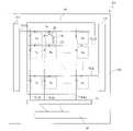
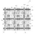
図1は、アクティブマトリクス基板101の平面構造の一例を模式的に示す図である。アクティブマトリクス基板101は、表示に寄与する表示領域DRと、表示領域DRの外側に位置する周辺領域(額縁領域)FRとを有している。表示領域DRは、行方向および列方向にマトリクス状に配列された複数の画素領域Pxを含む。画素領域Px(単に「画素」と呼ぶこともある)は、表示装置の画素に対応する領域である。非表示領域FRは、表示領域DRの周辺に位置し、表示に寄与しない領域である。 FIG. 1 is a diagram schematically showing an example of a planar structure of an
アクティブマトリクス基板101は、表示領域DRにおいて、基板1と、基板1に支持された複数のTFT(「画素TFT」とも呼ぶ。)20と、複数の画素電極PEと、TFT20にゲート信号を供給する複数のゲートバスラインGL(1)~GL(j)(jは2以上の整数、以下、「ゲートバスラインGL」と総称する)と、TFT20にソース信号を供給する複数のソースバスラインSL(1)~SL(k)(kは2以上の整数、以下、「ソースバスラインSL」と総称する)とを備える。各画素領域Pxは、例えばゲートバスラインGLおよびソースバスラインSLで規定されている。本明細書では、ソースバスラインSLの延びる方向を「列方向」、ゲートバスラインGLの延びる方向を「行方向」とする。行方向は、列方向と交差する方向であればよく、列方向に直交してなくてもよい。また、本明細書では、隣接する2つのソースバスラインSLの間に配列された複数の画素領域で構成される列を「画素列」、隣接する2つのゲートバスラインGLの間に配列された複数の画素領域で構成される行を「画素行」と呼ぶことがある。 The
各TFT20および各画素電極PEは、複数の画素領域Pxの1つに対応して設けられている。TFT20のゲート電極は、ゲートバスラインGLの1つに電気的に接続され、ソース電極は、ソースバスラインSLの1つに電気的に接続されている。ドレイン電極は、画素電極PEと電気的に接続されている。本実施形態では、TFT20は、例えば、トップゲート構造を有する複数の酸化物半導体TFTである。 Each
アクティブマトリクス基板101を、FFS(Fringe Field Switching)モードなどの横電界モードの表示装置に適用する場合には、アクティブマトリクス基板101に、複数の画素領域Pxに対して共通の電極(共通電極)CEが設けられる。 When the
非表示領域FRには、ドライバなどの周辺回路が設けられ得る。例えば、ゲートバスラインGLを駆動するゲートドライバGD、ソースバスラインSLを時分割で駆動するSSD回路Scなどがモノリシックに形成されていてもよい。SSD回路Scは、例えばCOG(Chip on Glass)方式で実装されたソースドライバSDに接続されている。 A peripheral circuit such as a driver may be provided in the non-display area FR. For example, a gate driver GD that drives the gate bus lines GL, an SSD circuit Sc that drives the source bus lines SL in a time division manner, and the like may be monolithically formed. The SSD circuit Sc is connected to a source driver SD implemented by, for example, a COG (Chip on Glass) method.
アクティブマトリクス基板101を用いた表示パネルは、例えば、アクティブマトリクス基板101と、対向基板と、これらの間に設けられた表示媒体層とを備える。表示媒体層は液晶層、有機EL層などであってもよい。 A display panel using the
アクティブマトリクス基板101を用いた表示パネルでは、線順次走査が行われる。線順次走査方式では、画素電極PEに供給されるデータ信号(表示信号ともいう。)は、ゲートドライバGDからゲートバスラインGLに供給される制御信号によって選択されたTFT20がオン状態となったときに、そのTFT20に接続されているソースバスラインSLに供給されている信号である。したがって、あるゲートバスラインGLに接続されているTFT20が同時にオン状態となり、その時に、その行の画素領域PxのそれぞれのTFT20に接続されているソースバスラインSLから対応するデータ信号が供給される。この動作を、例えば表示面の最も上側に位置する画素行から最も下側に位置する画素行まで順次行うことによって、表示領域DRに1枚の画像(フレーム)が書き込まれ、表示される。なお、1つの画素行が選択されて、次の行が選択されるまでの時間は水平走査期間(1H)と呼ばれ、ある行が選択され、再びその行が選択されるまでの時間は垂直走査期間(1V)またはフレームと呼ばれる。 A display panel using the
また、表示パネルでは、通常、交流駆動される。典型的には、データ信号の極性を1フレーム毎(1垂直走査期間毎)に反転する、フレーム反転駆動が行われる。例えば、1/60sec毎に極性反転が行われている(極性反転の周期は30Hz)。1フレーム内においても印加される電圧の極性の異なる画素を均一に分布させるために、ドット反転駆動、カラム反転(ソースライン反転)駆動などが行われている。ドット反転駆動は、データ信号の極性を1フレーム毎に反転させ、かつ、垂直・水平方向に隣り合う画素の極性を反転させる駆動方式である。カラム反転駆動は、画素電圧の極性を1フレーム毎かつ所定本数のソースバスライン毎に反転させる駆動方式である。さらに、画素とその画素に対応するソースバスラインSLとの位置関係が画素行ごとに異なるように構成された表示パネルにおいて、1フレームごとにソースバスラインSLの極性を反転させる駆動方式(Z反転(Z inversion)駆動方式ともいう。)も知られている。このような方式は、例えば特開2001-33757号公報、国際公開第2011/093374号などに開示されている。参考のため、特開2001-33757号公報および国際公開第2011/093374号の全開示内容を本願明細書に援用する。 In addition, the display panel is usually AC-driven. Typically, frame inversion driving is performed in which the polarity of the data signal is inverted every frame (every vertical scanning period). For example, polarity reversal is performed every 1/60 sec (period of polarity reversal is 30 Hz). Dot inversion driving, column inversion (source line inversion) driving, and the like are performed in order to uniformly distribute pixels having different polarities of voltages applied within one frame. Dot inversion driving is a driving method in which the polarity of a data signal is inverted for each frame and the polarities of adjacent pixels in the vertical and horizontal directions are inverted. Column inversion driving is a driving method in which the polarity of a pixel voltage is inverted every frame and every predetermined number of source bus lines. Furthermore, in a display panel configured such that the positional relationship between the pixels and the source bus lines SL corresponding to the pixels is different for each pixel row, a driving method in which the polarity of the source bus lines SL is inverted for each frame (Z inversion) is used. (also referred to as a Z inversion drive method) is also known. Such a method is disclosed, for example, in Japanese Unexamined Patent Publication No. 2001-33757 and International Publication No. 2011/093374. For reference, the entire disclosures of JP 2001-33757 A and WO 2011/093374 are incorporated herein by reference.
カラム反転駆動、Z反転駆動、ドット反転駆動などの駆動方式が適用された表示パネルでは、複数のソースバスラインSLのうちの一部のソースバスラインSLには、第1極性のデータ信号(以下、「第1データ信号」と呼ぶ)が供給され、他のソースバスラインSLには、第1極性とは逆の第2極性のデータ信号(以下、「第2データ信号」と呼ぶ)が供給される。第1および第2データ信号の極性は、フレームごとに反転する。本明細書では、第1データ信号が供給されるソースバスラインSLを「第1極性ソースバスライン」、第2データ信号が供給されるバスラインSLを「第2極性ソースバスライン」とすると、第1極性ソースバスラインと第2極性ソースバスラインとは、例えば、Z本(Zは1以上の整数、例えばZ=1)おきに交互に配列される。 In a display panel to which a driving method such as column inversion driving, Z inversion driving, or dot inversion driving is applied, some of the plurality of source bus lines SL have a data signal of a first polarity (hereinafter referred to as , referred to as a "first data signal"), and the other source bus line SL is supplied with a data signal having a second polarity opposite to the first polarity (hereinafter referred to as a "second data signal"). be done. The polarities of the first and second data signals are reversed every frame. In this specification, the source bus line SL supplied with the first data signal is referred to as the "first polarity source bus line", and the bus line SL supplied with the second data signal is referred to as the "second polarity source bus line". The first polarity source bus lines and the second polarity source bus lines are alternately arranged, for example, every Z lines (Z is an integer equal to or greater than 1, eg, Z=1).
<アクティブマトリクス基板101の画素領域の構造>
以下、図面を参照しながら、FFSモードの表示装置に適用されるアクティブマトリクス基板を例に、本実施形態のアクティブマトリクス基板101の画素領域の構造を説明する。FFSモードは、一方の基板に一対の電極を設けて、液晶分子に、基板面に平行な方向(横方向)に電界を印加する横方向電界方式のモードである。<Structure of Pixel Region of
The structure of the pixel region of the
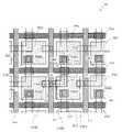
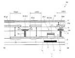
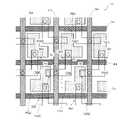
図2Aは、アクティブマトリクス基板101における一部の画素領域Pxを例示する平面図である。図2Bは、図2Aに示すIIb-IIb’線に沿った断面図である。 FIG. 2A is a plan view illustrating a partial pixel region Px on the
アクティブマトリクス基板101は、基板1と、基板1に支持された複数のソースバスラインSLおよび複数のゲートバスラインGLとを備える。ソースバスラインSLは列方向に延び、ゲートバスラインGLは行方向に延びている。この例では、各画素領域Pxは、隣接する2つのソースバスラインSLおよび隣接する2つのゲートバスラインGLによって画定されている。 The
図2Aでは、複数のゲートバスラインGLのうち、図の上側からこの順で配列されたゲートバスラインGLa、GLb、GLcと、複数のソースバスラインSLのうち、図の左側からこの順で配置されたソースバスラインSLa、SLb、SLcとを示す。また、これらのバスラインによって画定された6つの画素領域Px(a1)~Px(c2)を示す。画素領域Px(a1)、Px(b1)、Px(c1)は、ゲートバスラインGLaとゲートバスラインGLbとの間に、図の左側から行方向に配置されている。画素領域Px(a2)、Px(b2)、Px(c2)は、ゲートバスラインGLbとゲートバスラインGLcとの間に、図の左側から行方向に配置されている。画素領域Px(a2)、Px(b2)、Px(c2)は、それぞれ、画素領域Px(a1)、Px(b1)、Px(c1)と列方向に隣接している。 In FIG. 2A, among the plurality of gate bus lines GL, gate bus lines GLa, GLb, and GLc are arranged in this order from the upper side of the drawing, and among the plurality of source bus lines SL, they are arranged in this order from the left side of the drawing. connected source bus lines SLa, SLb, SLc. Also shown are six pixel regions Px(a1) to Px(c2) defined by these bus lines. The pixel regions Px(a1), Px(b1), and Px(c1) are arranged in the row direction from the left side of the figure between the gate bus lines GLa and GLb. The pixel regions Px(a2), Px(b2), and Px(c2) are arranged in the row direction from the left side of the figure between the gate bus lines GLb and GLc. Pixel regions Px(a2), Px(b2), and Px(c2) are adjacent to pixel regions Px(a1), Px(b1), and Px(c1) in the column direction, respectively.
各画素領域Pxは、画素電極PEおよびTFT20を有する。この例では、画素領域Px(a1)は、画素電極PEa1およびTFT20a1を有する。画素電極PEa1は、画素領域Px内に配置されている。TFT20a1は、画素領域Px(a1)に対応付けて配置されており、TFT20a1の一部は他の画素領域まで延びている。同様に、画素領域Px(a2)、Px(b1)、Px(b2)、Px(c1)、Px(c2)は、それぞれ、その画素領域内に配置された画素電極PEa2、PEb1、PEb2、PEc1、PEc2と、その画素領域に対応付けて配置されたTFT20a2、20b1、20b2、20c1、30c2を有する。 Each pixel region Px has a pixel electrode PE and a TFT20. In this example, pixel region Px(a1) has pixel electrode PEa1 and TFT 20a1. The pixel electrode PEa1 is arranged in the pixel region Px. The TFT 20a1 is arranged in association with the pixel region Px(a1), and part of the TFT 20a1 extends to another pixel region. Similarly, pixel regions Px(a2), Px(b1), Px(b2), Px(c1), and Px(c2) have pixel electrodes PEa2, PEb1, PEb2, and PEc1 arranged in the pixel regions, respectively. , PEc2, and TFTs 20a2, 20b1, 20b2, 20c1, and 30c2 arranged in association with the pixel regions.
本実施形態では、同じ画素列に配置された画素電極PEは、対応するTFT20を介して同じソースバスラインSLに電気的に接続されている。この例では、画素電極PEa1、PEa2は、TFT20a1、20a2を介してソースバスラインSLaに接続されている。同様に、画素電極PEb1、PEb2は、TFT20b1、20b2を介してソースバスラインSLbに接続され、画素電極PEc1、PEc2は、TFT20c1、20c2を介してソースバスラインSLcに接続されている。 In this embodiment, the pixel electrodes PE arranged in the same pixel column are electrically connected to the same source bus line SL via the corresponding
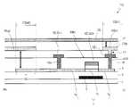
次いで、図2Aおよび図2Bを参照して、ソースバスラインSLbおよびSLc、ゲートバスラインGLaおよびGLbによって画定された画素領域Px(b1)を例に、画素領域PxおよびTFT20の構造をより具体的に説明する。 Next, referring to FIGS. 2A and 2B, the pixel region Px (b1) defined by the source bus lines SLb and SLc and the gate bus lines GLa and GLb is taken as an example, and the structures of the pixel region Px and the
画素領域Px(b1)は、基板1と、基板1に支持されたTFT20b1と、画素電極PEb1と、共通電極CEとを有している。TFT20b1は、画素領域Px(b1)に対応付けられて配置されているが、TFT20b1の一部は、他の画素領域(この例では画素領域Px(b2)、Px(a2))に位置している。 The pixel region Px(b1) has a
図2Bに示すように、TFT20b1は、酸化物半導体層7と、酸化物半導体層7の一部上にゲート絶縁層9を介して配置されたゲート電極GEとを備える。TFT20b1は、ソース電極SEおよびドレイン電極DEをさらに有し得る。 As shown in FIG. 2B, the TFT 20b1 includes an
酸化物半導体層7は、チャネル領域7cと、その両側にそれぞれ配置された第1領域7sおよび第2領域7dとを含む。第1領域7sおよび第2領域7dは、チャネル領域7cよりも比抵抗の小さい低抵抗領域である。第1領域7sは、対応するソースバスラインSLbに電気的に接続され、第2領域7dは、画素電極PEb1に電気的に接続されている。この例では、第1領域7sはソース電極SEに接続され、ソース電極SEを介してソースバスラインSLbに電気的に接続されている。第2領域7dはドレイン電極DEに接続され、ドレイン電極DEを介して画素電極PEb1に電気的に接続されている。
ゲート電極GEは、基板1の主面の法線方向(以下、「基板1の法線方向」と略す。)から見たとき、チャネル領域7cと重なるように配置されている。ゲート電極GEは、ゲートバスラインGLと同じ導電膜(ゲート用導電膜)を用いて形成されている。本明細書では、ゲート用導電膜を用いて形成された電極・配線を含む層を「ゲートメタル層」と呼ぶ。ゲート電極GEは、対応するゲートバスラインGLbに電気的に接続されている。なお、ゲート電極GEは、対応するゲートバスラインGLと一体的に形成されていてもよい。例えば、ゲート電極GEは、対応するゲートバスラインGLに繋がっているか、またはその一部であってもよい。このような場合、ゲートバスラインGLのうち、基板1の法線方向から見たとき酸化物半導体層7に重なる部分を「ゲート電極GE」と呼ぶ。ゲート電極GEは、基板1の法線方向から見たとき、チャネル領域7cに重なるが、低抵抗領域(第1領域7sおよび第2領域7d)には重ならないように配置されていてもよい。 The gate electrode GE is arranged so as to overlap with the
ゲート絶縁層9は、チャネル領域7cを覆い、かつ、第1領域7sおよび第2領域7dを覆っていなくてもよい。このような構成は、酸化物半導体層7のうちゲート絶縁層9で覆われていない部分を低抵抗化させることで得られる。図示している例では、ゲート絶縁層9は、基板1の法線方向から見たときに、ゲートメタル層に重なる領域にのみ形成されている。つまり、ゲート絶縁層9のエッジは、ゲートメタル層のエッジと整合している。このような構成は、ゲートメタル層のパターニングと同じレジストマスクを用いて、またはゲート電極GEをマスクとして用いてゲート絶縁層をパターニングすることで得られる。
本実施形態では、酸化物半導体層7、ゲート絶縁層9およびゲートメタル層は、層間絶縁層10で覆われており、ソース電極SEおよびドレイン電極DEは、層間絶縁層10上に配置されている。層間絶縁層10は、酸化物半導体層7の第1領域7sおよび第2領域7dに接していてもよい。層間絶縁層10には、酸化物半導体層7の第1領域7sの一部を露出する第1開口部10sと、第2領域7dの一部を露出する第2開口部10dとが設けられている。ソース電極SEは、層間絶縁層10上および第1開口部10s内に配置され、第1開口部10s内で第1領域7sに接続されている。ドレイン電極DEは、層間絶縁層10上および第2開口部10d内に配置され、第2開口部10d内で第2領域7dに接続されている。 In this embodiment, the
ソース電極SEおよびドレイン電極DEは、ソースバスラインSLと同じ導電膜(ソース用導電膜)を用いて形成されていてもよい。本明細書では、ソース用導電膜を用いて形成された電極・配線を含む層を「ソースメタル層」と呼ぶ。ソース電極SEは、対応するソースバスラインSLbに電気的に接続されている。なお、ソース電極SEは、対応するソースバスラインSLと一体的に形成されていてもよい。例えば、ソース電極SEは、対応するソースバスラインSLに繋がっているか、またはその一部であってもよい。このような場合、ソースバスラインSLのうち、第1領域7sに接する部分を「ソース電極SE」と呼ぶ。本明細書では、酸化物半導体層7の第1領域7sとソースバスラインSLとの接続部SCを「ソースコンタクト部」と呼ぶことがある。図示する例では、ソースコンタクト部SCは、ソースバスラインSLに重なるように配置されている。 The source electrode SE and the drain electrode DE may be formed using the same conductive film (source conductive film) as the source bus line SL. In this specification, a layer including electrodes and wirings formed using a source conductive film is referred to as a “source metal layer”. Source electrode SE is electrically connected to corresponding source bus line SLb. Note that the source electrode SE may be formed integrally with the corresponding source bus line SL. For example, the source electrode SE may be connected to or part of the corresponding source bus line SL. In such a case, a portion of the source bus line SL that is in contact with the
ドレイン電極DEは、対応する画素電極PEb1に電気的に接続されている。本明細書では、TFT20の第2領域7dと画素電極PEとの接続部PCを「画素コンタクト部」と呼ぶ。画素コンタクト部PCは、例えば画素領域Px(b1)内に配置されている。なお、ソースメタル層内にドレイン電極DEを設けずに、画素コンタクト部において、画素電極PEb1と第2領域7dの一部とを直接接触させてもよい。 The drain electrode DE is electrically connected to the corresponding pixel electrode PEb1. In this specification, the connecting portion PC between the
本実施形態では、基板1の法線方向から見たとき、各TFT20における酸化物半導体層7の第1領域7sは、列方向に隣接する画素領域Pxの画素電極PEに重なる部分X1と、隣接する画素列の画素領域(例えば行方向または斜め方向に隣接する画素領域)Pxの画素電極PEに重なる部分X2とを含む。これによって、追加の寄生容量C1、C2を形成している。 In the present embodiment, when viewed from the normal direction of the
図示する例では、画素領域Pxb1のTFT20b1における酸化物半導体層7の第1領域7sは、列方向に隣接する画素領域Px(b2)の画素電極PEb2に重なる部分X1と、斜め方向に隣接する画素領域Px(a2)の画素電極PEa2に重なる部分X2とを含む。酸化物半導体層7の部分X1と、画素電極PEb2と、これらの間に位置する絶縁層(ここでは層間絶縁層10および上部絶縁層13)とは、追加の寄生容量C1(b2)を構成している。同様に、酸化物半導体層7の部分X2と、画素電極PEa2と、これらの間に位置する絶縁層(ここでは層間絶縁層10および上部絶縁層13)とは、追加の寄生容量C2(a2)を構成している。ここではTFT20bを例に説明したが、他の画素領域PxのTFT20の酸化物半導体層7も同様に、列方向および斜め方向に隣接する画素領域Pxの画素電極PEとの間で追加の寄生容量C1、C2を構成し得る。つまり、1つの画素電極PEに着目すると、各画素電極PEは、他の画素領域PxのTFT20の酸化物半導体層7との間に、追加の寄生容量C1、C2を形成しているといえる。 In the illustrated example, the
本実施形態のTFT20は、上記の追加の寄生容量C1、C2が形成され得るように配置されていればよい。図2Aに示す例では、TFT20b1のチャネル長方向は、列方向(ソースバスラインSLの延びる方向)に略平行である(TFT縦置き構造)。この例では、TFT20b1の酸化物半導体層7は、基板1の法線方向から見たとき、画素領域(自画素)Px(b1)の画素コンタクト部PCから、ゲートバスラインGLbを横切って、自画素と列方向に隣接する画素領域Px(b2)を経由し、さらに、ソースバスラインSLbを横切って、自画素と斜め方向に隣接する画素領域Px(a2)内まで延びている。基板1の法線方向から見たとき、酸化物半導体層7のうちゲートバスラインGLb(またはゲートバスラインGLbに接続されたゲート電極GE)上に位置する部分がチャネル領域7cである。酸化物半導体層7のうちチャネル領域7cよりも画素コンタクト部PC側に位置する領域が第2領域7dであり、その反対側に位置する領域が第1領域7sである。第1領域7sは、ソースバスラインSLb(またはソースバスラインSLbに接続されたソース電極SE)上に設けられたソースコンタクト部SCで、ソースバスラインSLbに電気的に接続されている。酸化物半導体層7の第1領域7sは、基板1の法線方向から見たとき、列方向および斜め方向に隣接する画素領域Px(b2)、Px(a2)の画素電極PEb2、PEa2と部分的に重なっている。 The
TFT20b1は、酸化物半導体層7と基板1との間に位置する導電層3を有していてもよい。導電層3は、下部絶縁層5で覆われており、酸化物半導体層7は下部絶縁層5上に配置されていてもよい。導電層3は、基板1の法線方向から見たとき、酸化物半導体層7のうち少なくともチャネル領域7cと重なるように配置されていてもよい。これにより、基板1側からの光(バックライト光)に起因する酸化物半導体層7の特性劣化を抑制できる。導電層3は、電気的にフローティング状態であってもよいし、GND電位(0V)等に固定されていてもよい。あるいは、導電層3を、図示しない接続部によってゲート電極GEに電気的に接続することで、下部ゲート電極として機能させてもよい。 TFT 20
ソースメタル層の上には、上部絶縁層13が設けられている。上部絶縁層13は、例えば、無機絶縁層(パッシベーション膜)を含む。上部絶縁層13は、無機絶縁層と、無機絶縁層上に形成された有機絶縁層とを含む積層構造を有していてもよい。有機絶縁層は形成されていなくてもよい。あるいは、有機絶縁層は、表示領域にのみ形成されていてもよい。 An upper insulating
画素電極PEb1は、上部絶縁層13上に配置されている。画素電極PEb1は、隣接する画素電極PEから分離されている。画素電極PEb1は、上部絶縁層13に形成された画素コンタクトホールCHp内でTFT20b1のドレイン電極DEに電気的に接続されている。 The pixel electrode PEb1 is arranged on the upper insulating
画素電極PEb1上には、誘電体層17を介して共通電極CEが配置されている。図示していないが、共通電極CEには、各画素領域Pxにおいて、1つまたは複数のスリット(開口部)あるいは切り欠き部が設けられている。共通電極CEは、画素領域Pxごとに分離されていなくてもよい。図2Bに示すように、共通電極CEは、誘電体層17を介して各画素電極PE(ここでは画素電極PEb1)に部分的に重なり、補助容量Ct(ここでは補助容量Ct(b1))を形成している。補助容量Ctは、透明材料から構成されるので透明補助容量とも呼ばれる。 A common electrode CE is arranged over the pixel electrode PEb1 with a
<β値について>
上述したように、本実施形態では、各TFT20の低抵抗領域である第1領域7sを、基板1の法線方向から見たとき、他の画素領域Pxの画素電極PEに重なるように延ばすことで、他の画素領域Pxの画素電極PEと追加の寄生容量(ソース・ドレイン間容量)C1、C2を構成している。つまり、酸化物半導体層7の第1領域7sを、寄生容量を形成する透明容量電極としても機能させている。これにより、自ソース寄生容量および他ソース寄生容量の大きさを制御できるので、上述したβ値を小さく抑えることができる。<About β value>
As described above, in the present embodiment, the
以下、1つの画素領域(自画素)の画素電極PEについて、自ソース寄生容量および他ソース寄生容量Csd(A)、Csd(B)を説明する。ここでは、画素電極PEb2を例に説明する。 The self-source parasitic capacitance and other-source parasitic capacitances Csd(A) and Csd(B) for the pixel electrode PE of one pixel region (self-pixel) will be described below. Here, the pixel electrode PEb2 will be described as an example.
画素領域Px(b2)の画素電極PEb2は、自ソースバスラインSLbとの間に、斜め電界による通常寄生容量CA(b2)を形成し、他ソースバスラインSLcとの間に、斜め電界による通常寄生容量CB(b2)を形成している。さらに、画素電極PEb2は、列方向に隣接する画素領域Px(b1)におけるTFT20b1の酸化物半導体層7の部分X1との間に追加の寄生容量C1(b2)を形成し、かつ、斜め方向に隣接する画素領域Px(c1)におけるTFT20c1の酸化物半導体層7の部分X2との間に追加の寄生容量C2(b2)を形成している。この例では、追加の寄生容量C1(b2)は、自画素である画素電極PEb2と、自ソースバスラインであるソースバスラインSLbに接続された透明電極(TFT20b1の部分X1)とによって構成される自ソース寄生容量であり、上述した式(1)のCsd(A)に加算される。追加の寄生容量C2(b2)は、画素電極PEb2と、他ソースバスラインであるソースバスラインSLcに接続された透明電極(TFT20c1の部分X2)とによって構成される他ソース寄生容量であり、式(1)のCsd(B)に加算される。ここで、画素領域Px(b2)におけるCsd(A)、Csd(B)、ΔCsdを、それぞれ、Csd(A)b2、Csd(B)b2、ΔCsdb2とすると、追加の寄生容量C1(b2)、C2(b2)の大きさによって、Csd(A)b2、Csd(B)b2をそれぞれ独立して調整できるので、これらの差ΔCsdb2(絶対値)を低減できる。ΔCsdb2を小さく抑えることで、β値(式(1)で表されるβ(A-B))の絶対値を小さくすることが可能になる。
ΔCsdb2=|Csd(A)b2-Csd(B)b2|
Csd(A)b2:通常寄生容量CA(b2)および追加の寄生容量C1(b2)を含む。
Csd(B)b2:通常寄生容量CB(b2)および追加の寄生容量C2(b2)を含む。The pixel electrode PEb2 in the pixel region Px(b2) forms a normal parasitic capacitance CA(b2) due to an oblique electric field between its own source bus line SLb and a normal parasitic capacitance CA(b2) due to an oblique electric field between the other source bus line SLc. It forms a parasitic capacitance CB (b2). Furthermore, the pixel electrode PEb2 forms an additional parasitic capacitance C1 (b2) between it and the portion X1 of the
ΔCsdb2 = |Csd(A)b2 -Csd(B)b2 |
Csd(A)b2 : includes normal parasitic capacitance CA(b2) and additional parasitic capacitance C1(b2).
Csd(B)b2 : includes normal parasitic capacitance CB(b2) and additional parasitic capacitance C2(b2).
また、画素電極PEb2は、誘電体層17を介して共通電極CEと部分的に重なることで、補助容量Ct(b2)を形成している。補助容量Ct(b2)は、式(1)のCpiに加算されるので、β値をさらに低減できる。 In addition, the pixel electrode PEb2 partially overlaps the common electrode CE with the
追加の寄生容量C1、C2の大きさは、例えば、寄生容量を構成する電極の重なり面積を調整することで容易に調整され得る。各TFT20および各画素電極PEの配置によって、追加の寄生容量C1、C2を互いに独立して制御することが可能である。 The magnitudes of the additional parasitic capacitances C1 and C2 can be easily adjusted, for example, by adjusting the overlapping area of the electrodes forming the parasitic capacitances. The arrangement of each
追加の寄生容量C1、C2の面積(つまり、部分X1、X2の面積)は、特に限定しないが、それぞれ、画素電極PEの面積の0.1%以上10%以下であってもよい。なお、画素電極PEの面積は、例えば数百μm2~数千μm2であってもよい。酸化物半導体層7の配線幅(低抵抗領域の幅)は、特に限定しないが、例えば3μm程度であり得る。The areas of the additional parasitic capacitances C1 and C2 (that is, the areas of the portions X1 and X2) are not particularly limited, but may be 0.1% or more and 10% or less of the area of the pixel electrode PE. The area of the pixel electrode PE may be, for example, several hundred μm2 to several thousand μm2 . The wiring width (the width of the low-resistance region) of the
追加の寄生容量C1、C2の面積の大小関係は特に限定しない。例えば、追加の寄生容量以外の寄生容量において他ソース寄生容量の方が自ソース寄生容量よりも小さい場合には、寄生容量C2の面積を、寄生容量C1よりも大きくしてもよい。 There is no particular limitation on the size relationship of the areas of the additional parasitic capacitances C1 and C2. For example, if the other source parasitic capacitance is smaller than the own source parasitic capacitance among the parasitic capacitances other than the additional parasitic capacitance, the area of the parasitic capacitance C2 may be made larger than the parasitic capacitance C1.
各画素領域Pxのレイアウトは、図示する例に限定されない。TFT20および画素電極PEは、TFT20の酸化物半導体層7が、基板1の法線方向から見たとき、他の画素領域Pxの画素電極PEに重なる部分を有するように配置されていればよい。図示する例では、酸化物半導体層7は、基板1の法線方向から見たとき、列方向に延びる部分と行方向に延びる部分とから構成されるL字形であるが、酸化物半導体層7の平面形状はこれに限定されない。酸化物半導体層7は、例えば、斜め方向(列方向および行方向に交差する方向)に延びる部分を含んでもよいし、ソースバスラインSL上を重なって延びる部分を含んでもよい。また、後述するように、酸化物半導体層7は、列方向に隣接する他の画素領域の画素電極PEに重なっていなくてもよい(つまり、C1=0)。さらに、後述するように、TFT20は、チャネル長方向が行方向に概ね平行になるように配置されていてもよい(TFT横置き構造)。 The layout of each pixel region Px is not limited to the illustrated example. The
各画素領域Pxに配置される画素TFTは、基板に支持され、かつ、活性層として酸化物半導体層を有していればよい。この例では、画素TFTとして、ゲート電極GEと基板1との間に酸化物半導体層7が位置するトップゲート型のTFT20を用いているが、酸化物半導体層と基板との間にゲート電極が位置するボトムゲート型TFTであってもよい。ただし、トップゲート型TFTであれば、酸化物半導体層7のうちチャネル領域7c以外の領域を容易に低抵抗化することができ、この領域を、透明な容量電極として使用できるので有利である。 The pixel TFT arranged in each pixel region Px only needs to be supported by the substrate and have an oxide semiconductor layer as an active layer. In this example, a
本実施形態では、画素電極PE上に共通電極CEが配置されることが好ましい。画素電極PE上に共通電極CEが配置されていると、画素電極PEの基板1側に共通電極CEが配置される場合と比べて、画素電極PEと各ソースバスラインSLとの間に生じる通常寄生容量CA、CBが大きくなる。このため、追加の寄生容量C1、C2の形成によって、より効果的にβ値を小さくできる。なお、アクティブマトリクス基板は、共通電極CEを備えていなくてもよい。そのようなアクティブマトリクス基板は、縦電界モードの表示装置に適用され得る。縦電界モードの表示装置では、共通電極CEは対向基板側に設けられる。 In this embodiment, the common electrode CE is preferably arranged on the pixel electrode PE. When the common electrode CE is arranged on the pixel electrode PE, the normal voltage generated between the pixel electrode PE and each source bus line SL is greater than when the common electrode CE is arranged on the
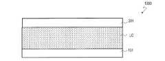
本実施形態のアクティブマトリクス基板101は、例えば液晶表示装置に適用され得る。図12は、アクティブマトリクス基板101を用いた液晶表示装置1000の模式的な断面図である。液晶表示装置1000は、アクティブマトリクス基板101と、アクティブマトリクス基板101に対向するように配置された対向基板201と、アクティブマトリクス基板101と対向基板201との間に設けられた液晶層LC層とを備える。 The
アクティブマトリクス基板101は、例えば、カラム反転駆動を行う液表表示装置に好適に使用され得る。カラム反転駆動方式の表示装置では、各画素列における複数の画素電極は、いずれも同じソースバスラインSLに接続されている。1つの画素列を構成する複数の画素電極には、同じ極性のデータ信号が書き込まれる。その画素列に隣接する画素列の画素電極には、反対の極性のデータ信号が書き込まれる。これにより、行方向に隣り合う画素同士で、画素電極の電圧の極性を異ならせることができる。カラム反転駆動を行う液晶表示装置に用いられるアクティブマトリクス基板では、上下に隣接する画素領域が同じソースバスラインSLに接続されている。このような配置では、他ソース寄生容量Csd(B)が、自ソース寄生容量Csd(A)よりも小さくなりやすい。これに対し、本実施形態では、追加の寄生容量C1の面積よりも追加の寄生容量C2の面積が大きくなるように、TFT20および画素電極PEを配置することで、自ソース寄生容量Csd(A)と他ソース寄生容量Csd(B)との差を小さくすることができ、β値の絶対値を低減できる。 The
本実施形態のアクティブマトリクス基板101は、例えば、低周波駆動を行う表示装置に特に好適に適用される。低周波駆動を行う場合、休止期間中の画素の輝度変化によってフリッカが発生しやすいので、追加の寄生容量C1、C2の形成によるフリッカ低減効果がより顕著に得られる。 The
本実施形態は、低周波駆動を行わない表示装置にも適用され得る。本実施形態によると、寄生容量による画素電位の変動を低減できることから、低周波駆動を行わない場合であっても、画素電位の変動によるフリッカの発生や表示品位の低下を抑制し得る。β値またはΔCsdの好ましい範囲は、駆動周波数によって異なり得る。例えば、駆動周波数が低いほど、β値の絶対値をより小さく(0に近く)することが求められる。本実施形態によると、駆動方法や駆動周波数に応じて要求されるβ値が得られるように、追加の寄生容量C1、C2の大きさを調整すればよいので、種々の表示装置に広く適用され得る。 This embodiment can also be applied to a display device that does not perform low-frequency driving. According to the present embodiment, since fluctuations in pixel potential due to parasitic capacitance can be reduced, flicker due to fluctuations in pixel potential and deterioration in display quality can be suppressed even when low-frequency driving is not performed. A preferred range for the β value or ΔCsd may vary depending on the drive frequency. For example, the lower the drive frequency, the smaller the absolute value of the β value (closer to 0). According to this embodiment, the size of the additional parasitic capacitances C1 and C2 can be adjusted so as to obtain the required β value according to the driving method and driving frequency. obtain.
本実施形態は、高精細なアクティブマトリクス基板に特に好適に適用され得る。高精細化に伴い、上記式(1)のCpiが小さくなるため、β値が大きくなりやすい。このため、追加の寄生容量C1、C2の形成によって、β値をより効果的に改善できる。 This embodiment can be applied particularly suitably to a high-definition active matrix substrate. Since Cpi in the above formula (1) becomes smaller with higher definition, the β value tends to increase. Therefore, the formation of the additional parasitic capacitances C1 and C2 can improve the β value more effectively.
(変形例)
以下、図面を参照しながら、本実施形態のアクティブマトリクス基板の変形例を説明する。以降の図面では、図2A、図2Bと同様の構成要素には同じ参照符号を付している。同様の構成要素については、適宜説明を省略する。(Modification)
Modifications of the active matrix substrate of this embodiment will be described below with reference to the drawings. In subsequent drawings, the same reference numerals are given to the same components as in FIGS. 2A and 2B. Description of similar components will be omitted as appropriate.
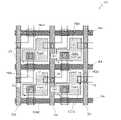
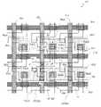
<変形例1>
変形例1は、各画素電極PEが、追加の寄生容量C2を形成するが、追加の寄生容量C1を形成しない点で、アクティブマトリクス基板101と異なる。<
図3Aは、変形例1のアクティブマトリクス基板102における一部の画素領域を例示する平面図であり、図2Aと同様に、6つの画素領域Px(a1)~Px(c2)を示す。図3Bは、図3Aに示すIIIb-IIIb’線に沿った断面図である。 FIG. 3A is a plan view illustrating a partial pixel region in the
変形例1は、基板1の法線方向から見たとき、各TFT20の酸化物半導体層7の第1領域7sは、斜め方向に隣接する他の画素領域Pxの画素電極PEに重なる部分X2を有する。部分X2と、他の画素領域Pxの画素電極PEと、これらの間に位置する絶縁層とは、他ソース寄生容量となる追加の寄生容量C2を構成している。各TFT20の酸化物半導体層7は、列方向に隣接する画素領域Pxの画素電極PEには重なっていない。 In Modified Example 1, when viewed from the normal direction of the
例えば、TFT20b1の酸化物半導体層7は、基板1の法線方向から見たとき、斜め方向に隣接する画素領域Px(a2)内で、画素電極PEa2と部分的に重なっており、画素電極PEa2との間に追加の寄生容量C2(a2)を形成している。TFT20b1の酸化物半導体層7の一部は、列方向に隣接する画素領域Px(b2)内に位置するが、画素電極PEb2には重なっていない。従って、画素電極PEb2との間に寄生容量(重なり容量)は形成されていない。 For example, when viewed from the normal direction of the
本実施形態によると、追加の寄生容量C2の大きさを調整することで、他ソース寄生容量Csd(B)を所定の量増加させることができる。従って、Csd(A)に対してCsd(B)が小さいときに、Csd(B)を増加させることで、式(1)のβ値の絶対値を小さくできる。 According to this embodiment, by adjusting the size of the additional parasitic capacitance C2, the other source parasitic capacitance Csd(B) can be increased by a predetermined amount. Therefore, when Csd(B) is smaller than Csd(A), increasing Csd(B) can reduce the absolute value of the β value in equation (1).
例えば、画素領域Px(b2)を自画素とすると、Csd(A)b2、Csd(B)b2は、それぞれ、自画素の画素電極PEb2とソースバスラインSLbおよびソースバスラインSLcとの間に形成される通常寄生容量CA(b2)、CB(b2)を含む。Csd(B)b2は、さらに、自画素の画素電極PEb2と、斜めに隣接する画素領域Px(c1)のTFT20c1の酸化物半導体層7との間に形成される追加の寄生容量C2(b2)を含む。従って、C2(b2)によって、Csd(A)b2とCsd(B)b2との差ΔCsdb2(絶対値)を調整できる。
ΔCsdb2=|Csd(A)b2-Csd(B)b2|
Csd(A)b2:通常寄生容量CA(b2)を含む。
Csd(B)b2:通常寄生容量CB(b2)および追加の寄生容量C2(b2)を含む。For example, if the pixel region Px(b2) is the own pixel, Csd(A)b2 and Csd(B)b2 are formed between the pixel electrode PEb2 of the own pixel and the source bus line SLb and the source bus line SLc, respectively. including normal parasitic capacitances CA(b2), CB(b2). Csd(B)b2 is further an additional parasitic capacitance C2(b2) formed between the pixel electrode PEb2 of its own pixel and the
ΔCsdb2 = |Csd(A)b2 -Csd(B)b2 |
Csd(A)b2 : Usually includes parasitic capacitance CA(b2).
Csd(B)b2 : includes normal parasitic capacitance CB(b2) and additional parasitic capacitance C2(b2).
図4および図5は、それぞれ、本変形例の他のアクティブマトリクス基板103、104を示す平面図である。 4 and 5 are plan views showing other
図4に例示するように、TFT20の酸化物半導体層7の平面形状は、アクティブマトリクス基板101と同様であり、画素電極PEが、追加の寄生容量C1を形成しないように(列方向に隣接する画素領域Pxの酸化物半導体層7と重ならないように)切欠き部を有していてもよい。 As illustrated in FIG. 4, the planar shape of the
あるいは、図5に例示するように、TFT20は、そのチャネル長方向が行方向(ゲートバスラインGLの延びる方向)に略平行となるように配置されていてもよい(TFT横置き構造)。この場合、TFT20の酸化物半導体層7は、基板1の法線方向から見たとき、行方向に隣接する画素領域Pxの画素電極PEに部分的に重なるように延びることによって、追加の寄生容量C2が形成されてもよい。 Alternatively, as illustrated in FIG. 5, the
図5に示すTFT20c2を例に説明すると、TFT20c2の酸化物半導体層7は、基板1の法線方向から見たとき、画素コンタクト部PCからゲート電極GE(ここでは、ゲートバスラインGLbの枝部)に重なるように行方向に延びている。酸化物半導体層7のうちゲート電極GEに重なる部分がチャネル領域となる。酸化物半導体層7の第1領域は、基板1の法線方向から見たとき、ソースバスラインSLcを横切って、行方向に隣接する他の画素領域Pxb2内において、画素電極PEb2に重なる部分X2を有する。部分X2と、画素電極PEb2と、その間に位置する絶縁層とによって、追加の寄生容量C2(b2)が形成される。 Taking the TFT 20c2 shown in FIG. 5 as an example, the
<変形例2>
変形例2は、例えば、Z反転駆動方式の液晶表示装置に用いられるアクティブマトリクス基板である。Z反転駆動方式を行うことで、行方向のみでなく、列方向に隣り合う画素同士でも、画素電極の電圧の極性を異ならせることができる。<
図6Aは、変形例2のアクティブマトリクス基板105における一部の画素領域を例示する平面図であり、図2Aと同様に、6つの画素領域Px(a1)~Px(c2)を示す。図6Bは、図6Aに示すIV-IV’線における断面図である。 FIG. 6A is a plan view illustrating a partial pixel region in the
アクティブマトリクス基板105では、各画素電極PEは、列方向および行方向に隣接する画素領域の画素電極PEとは異なるソースバスラインSLに接続されている。この例では、右側に位置するソースバスラインSLに接続された画素電極PEからなる画素行と、左側に位置するソースバスラインSLに接続された画素電極PEからなる画素行とが、列方向に交互に配置されている。 In the
アクティブマトリクス基板104でも、アクティブマトリクス基板101と同様に、基板1の法線方向から見たとき、各TFT20の酸化物半導体層7は、列方向に隣接する画素領域Pxの画素電極PEに重なる部分X3と、斜め方向に隣接する画素領域Pxの画素電極PEに重なる部分X4とを有する。例えば、画素領域Px(b1)のTFT20b1の酸化物半導体層7の第1領域7sは、列方向に隣接する画素領域Px(b2)の画素電極PEb2に重なる部分X3と、斜め方向に隣接する画素領域Px(a2)の画素電極PEa2に重なる部分X4とを有する。部分X3は、画素領域Px(b2)の画素電極PEb2と、絶縁層(ここでは層間絶縁層10および上部絶縁層13)を介して重なることにより、追加の寄生容量C3(b2)を構成している。同様に、部分X4は、画素領域Px(a2)の画素電極PEa2と、絶縁層(ここでは層間絶縁層10および上部絶縁層13)を介して重なることにより、追加の寄生容量C4(a2)を構成している。ここでは、TFT20b1を例に説明したが、他の画素領域PxのTFT20の酸化物半導体層7も同様に、列方向および斜め方向に隣接する画素領域Pxの画素電極PEとの間で追加の寄生容量C3、C4を構成し得る。 In the
ここで、画素領域Px(b2)を自画素としてβ値を説明する。画素領域Px(b2)の画素電極PEb2は、自ソースバスラインであるソースバスラインSLcとの間に、通常寄生容量CA(b2)、他ソースバスラインであるソースバスラインSLbとの間に、通常寄生容量CB(b2)を有する。また、画素電極PEb2は、列方向に隣接する画素領域Px(b1)におけるTFT20b1の酸化物半導体層7との間に追加の寄生容量C3(b2)を形成し、かつ、斜め方向に隣接する画素領域Px(c1)におけるTFT20c1の酸化物半導体層7と追加の寄生容量C4(b2)を形成している。本変形例では、追加の寄生容量C3(b2)は、画素電極PEb2と、他ソースバスラインに接続された透明電極(TFT20b1の第1領域7s)とによって構成される他ソース寄生容量であり、式(1)のCsd(B)に加算される。追加の寄生容量C4(b2)は、画素電極PEb2と、自ソースバスラインに接続された透明電極(TFT20c1の第1領域7s)とによって構成される自ソース寄生容量であり、式(1)のCsd(A)に加算される。従って、本変形例でも、追加の寄生容量C3(b2)、C4(b2)の大きさによって、Csd(A)b2、Csd(B)b2をそれぞれ独立して調整できるので、これらの差ΔCsdb2(絶対値)を低減できる。
ΔCsdb2=|Csd(A)b2-Csd(B)b2|
Csd(A)b2:通常寄生容量CA(b2)および追加の寄生容量C4(b2)を含む。
Csd(B)b2:通常寄生容量CB(b2)および追加の寄生容量C3(b2)を含む。Here, the β value will be described with the pixel region Px(b2) as the own pixel. The pixel electrode PEb2 in the pixel region Px(b2) has a normal parasitic capacitance CA(b2) between it and the source bus line SLc that is its own source bus line, and between it and the source bus line SLb that is another source bus line: It usually has a parasitic capacitance CB(b2). Further, the pixel electrode PEb2 forms an additional parasitic capacitance C3 (b2) between itself and the
ΔCsdb2 = |Csd(A)b2 -Csd(B)b2 |
Csd(A)b2 : includes normal parasitic capacitance CA(b2) and additional parasitic capacitance C4(b2).
Csd(B)b2 : includes normal parasitic capacitance CB(b2) and additional parasitic capacitance C3(b2).
なお、図6Aおよび図6Bに示す例では、追加の寄生容量C3および追加の寄生容量C4を形成しているが、画素電極PEまたは酸化物半導体層7の配置や形状によって、追加の寄生容量C3および追加の寄生容量C4のうちいずれか一方のみを形成してもよい。例えば図7に例示するように、画素電極PEに、列方向に隣接する画素領域から延びる酸化物半導体層7と重ならないように切欠き部を設け、追加の寄生容量C3のみを形成してもよい。 In the examples shown in FIGS. 6A and 6B, the additional parasitic capacitance C3 and the additional parasitic capacitance C4 are formed. and additional parasitic capacitance C4. For example, as illustrated in FIG. 7, the pixel electrode PE may be provided with a notch so as not to overlap with the
また、図示しないが、画素TFTの横置き構造(図5参照)を採用し、画素TFTの酸化物半導体層を、基板の法線方向から見たとき、行方向に隣接する画素領域の画素電極に重なるように延伸させることで、追加の寄生容量を形成してもよい。本変形例では、行方向に隣接する画素領域の画素電極は、他ソースバスラインに接続されているので、追加の寄生容量は、他ソース寄生容量となる。 In addition, although not shown, the horizontal arrangement structure (see FIG. 5) of the pixel TFT is adopted, and when the oxide semiconductor layer of the pixel TFT is viewed from the normal direction of the substrate, the pixel electrodes of the pixel regions adjacent to each other in the row direction are arranged. Additional parasitic capacitance may be formed by extending the . In this modification, the pixel electrodes of the pixel regions adjacent in the row direction are connected to the other source bus line, so the additional parasitic capacitance is the other source parasitic capacitance.
<変形例3>
変形例3では、基板1の法線方向から見たとき、画素電極PEを、自ソースバスラインSLおよび/または他ソースバスラインSLに部分的に重なるように配置することで、自ソース寄生容量および/または他ソース寄生容量となる重なり容量を形成する。<
In
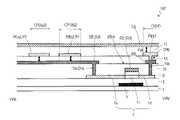
図8Aは、変形例3のアクティブマトリクス基板107における一部の画素領域を例示する平面図であり、図2Aと同様に、画素領域Px(a1)~Px(c2)を示す。図8Bは、図8Aに示すVIIIb-VIIIb’線に沿った断面図である。 FIG. 8A is a plan view illustrating a partial pixel region in the
アクティブマトリクス基板107は、基板1の法線方向から見たとき、各画素電極PEが、両側に位置する2つのソースバスラインSLに重なる部分P1、P2を有する点で、変形例1のアクティブマトリクス基板102と異なる。この例では、部分P1は、2つのソースバスラインSLのうち自ソースバスラインに重なる部分であり、部分P2は、他ソースバスラインに重なる部分である。 The
画素電極PEの部分P1、自ソースバスライン、およびその間に位置する絶縁層(ここでは上部絶縁層13)によって、寄生容量CP1が形成されている。同様に、画素電極PEの部分P2、他ソースバスライン、およびその間に位置する絶縁層(ここでは上部絶縁層13)によって、寄生容量CP2が形成されている。寄生容量CP1は、自ソース寄生容量Csd(A)となり、寄生容量CP2は、他ソース寄生容量Csd(B)となる。 A parasitic capacitance CP1 is formed by the portion P1 of the pixel electrode PE, its own source bus line, and the insulating layer (here, the upper insulating layer 13) located therebetween. Similarly, a parasitic capacitance CP2 is formed by the portion P2 of the pixel electrode PE, the other source bus line, and the insulating layer (here, the upper insulating layer 13) located therebetween. The parasitic capacitance CP1 becomes the own source parasitic capacitance Csd(A), and the parasitic capacitance CP2 becomes the other source parasitic capacitance Csd(B).
図示する例では、画素電極PEb2を例に説明すると、画素電極PEb2は、基板1の法線方向から見たとき、ソースバスラインSLbおよびソースバスラインSLc上まで延びる部分(延設部)P1、P2を有する。これにより、画素電極PEb2と、自ソースバスラインであるソースバスラインSLbとの間に寄生容量CP1(b2)を形成し、画素電極PEb2と、他ソースバスラインであるソースバスラインSLcとの間に寄生容量CP2(b2)を形成している。他の画素電極PEも同様に、両側に位置するソースバスラインSLとの間に寄生容量CP1、CP2を形成している。 In the illustrated example, taking the pixel electrode PEb2 as an example, the pixel electrode PEb2 has a portion (extended portion) P1 extending over the source bus line SLb and the source bus line SLc when viewed from the normal direction of the
図8Bから分かるように、各寄生容量CP1、CP2では、誘電体となる絶縁層が上部絶縁層13のみであり、他の追加の寄生容量C1~C4よりも薄い。このため、重なり面積が小さくても、十分な容量を確保し得る。各寄生容量CP1、CP2の重なり面積を調整することで、自ソース寄生容量Csd(A)と他ソース寄生容量Csd(B)との差をさらに低減できる。 As can be seen from FIG. 8B, each of the parasitic capacitors CP1 and CP2 has only the upper insulating
例えば、画素電極PEb2を自画素の画素電極とすると、Csd(A)b2は、通常寄生容量CA(b2)および寄生容量CP1(b2)を含み、Csd(B)b2は、通常寄生容量CB(b2)、追加の寄生容量C2(b2)および寄生容量CP2(b2)を含む。従って、C2(b2)のみでなく、寄生容量CP1(b2)、CP2(b2)によって、Csd(A)b2とCsd(B)b2との差ΔCsdb2(絶対値)を調整できる。
ΔCsdb2=|Csd(A)b2-Csd(B)b2|
Csd(A)b2:通常寄生容量CA(b2)および寄生容量CP1(b2)を含む。
Csd(B)b2:通常寄生容量CB(b2)、追加の寄生容量C2(b2)および寄生容量CP2(b2)を含む。For example, if the pixel electrode PEb2 is the pixel electrode of its own pixel, Csd(A)b2 normally includes parasitic capacitance CA(b2) and parasitic capacitance CP1(b2), and Csd(B)b2 normally includes parasitic capacitance CB( b2), including an additional parasitic capacitance C2 (b2) and a parasitic capacitance CP2 (b2). Therefore, the difference ΔCsdb2 (absolute value) between Csd(A)b2 and Csd(B)b2 can be adjusted not only by C2(b2) but also by parasitic capacitances CP1(b2) and CP2(b2).
ΔCsdb2 = |Csd(A)b2 -Csd(B)b2 |
Csd(A)b2 : normally includes parasitic capacitance CA(b2) and parasitic capacitance CP1(b2).
Csd(B)b2 : includes normal parasitic capacitance CB(b2), additional parasitic capacitance C2(b2) and parasitic capacitance CP2(b2).
寄生容量CP1、CP2を形成する場合には、各画素電極PEの部分P1が、それぞれ、隣接する画素電極PEの部分P2に重ならないように配置することが好ましい。1つのソースバスラインSL上において、その両側に位置する2つの画素電極PEの部分P1、P2は、例えば、列方向に間隔を空けて配置されてもよい。各部分P1、P2の行方向の幅は、ソースバスラインSLの幅の1/2以上であってもよい。 When forming the parasitic capacitances CP1 and CP2, it is preferable to arrange the portion P1 of each pixel electrode PE so as not to overlap the portion P2 of the adjacent pixel electrode PE. The two pixel electrode portions P1 and P2 located on both sides of one source bus line SL may be spaced apart in the column direction, for example. The width of each of the portions P1 and P2 in the row direction may be 1/2 or more of the width of the source bus line SL.
本変形例の構成は、図8Aおよび図8Bに示す構成に限定されない。例えば、各画素電極PEは、自ソースバスラインおよび他ソースバスラインに重なる部分P1、P2のいずれか一方のみを有してもよい。 The configuration of this modification is not limited to the configuration shown in FIGS. 8A and 8B. For example, each pixel electrode PE may have only one of the portions P1 and P2 overlapping its own source bus line and other source bus lines.
図9は、変形例3の他のアクティブマトリクス基板108における一部の画素領域を例示する平面図である。アクティブマトリクス基板108では、各画素電極PEは、基板1の法線方向から見たとき、他ソースバスラインに重なる部分P2を有する点で、図2Aおよび図2Bに示すアクティブマトリクス基板101と異なる。アクティブマトリクス基板108の各画素電極PEは、自ソースバスラインに重なる部分を有していない。また、追加の寄生容量C2に加えて、追加の寄生容量C1も形成されている。 FIG. 9 is a plan view illustrating a partial pixel region in another
この例では、例えば、画素電極PEb2を自画素の画素電極とすると、Csd(A)b2は、通常寄生容量CA(b2)および追加の寄生容量C1(b2)を含み、Csd(B)b2は、通常寄生容量CB(b2)、追加の寄生容量C2(b2)および寄生容量CP2(b2)を含む。例えば、他ソース寄生容量が自ソース寄生容量よりも小さい場合に本構成を採用すると、他ソース寄生容量Csd(B)のみを増加させることができるので有利である。In this example, for example, if the pixel electrode PEb2 is the pixel electrode of its own pixel, Csd(A)b2 includes normal parasitic capacitance CA(b2) and additional parasitic capacitance C1(b2), and Csd(B)b2 is , normal parasitic capacitance CB(b2), additional parasitic capacitance C2(b2) and parasitic capacitance CP2(b2). For example, when the other source parasitic capacitance is smaller than the own source parasitic capacitance, if this configuration is adopted, it is advantageous because only the other source parasitic capacitance Csd(B) can be increased.
図8Aおよび図9では、画素電極PEをソースバスラインSL上に延設させることで、寄生容量CP1、CP2を形成しているが、代わりに、ソースバスラインSLに、基板1の法線方向から見たとき、その両側または片側に位置する画素電極PEに重なる延設部を設けるか、あるいは、画素電極PEに重なるように屈曲させることで、寄生容量CP1および/または寄生容量CP2を形成してもよい。 In FIGS. 8A and 9, the parasitic capacitances CP1 and CP2 are formed by extending the pixel electrodes PE over the source bus lines SL. When viewed from above, the parasitic capacitance CP1 and/or the parasitic capacitance CP2 are formed by providing extended portions that overlap the pixel electrodes PE located on both sides or one side thereof, or by bending them so as to overlap the pixel electrodes PE. may
さらに、本変形例のアクティブマトリクス基板は、前述した追加の寄生容量C1~C4の少なくとも1つと、寄生容量CP1、CP2の少なくとも一方とを有していればよく、どのように組み合わせても構わない。これにより、レイアウトの自由度を高めつつ、所望のβ値を実現し得る。 Furthermore, the active matrix substrate of this modified example only needs to have at least one of the additional parasitic capacitances C1 to C4 and at least one of the parasitic capacitances CP1 and CP2 described above, and may be combined in any way. . As a result, a desired β value can be achieved while increasing the degree of freedom in layout.
<変形例4>
変形例4では、画素TFTの酸化物半導体層と画素電極との寄生容量を形成せず、寄生容量CP1および/または寄生容量CP2を形成する点で、変形例3のアクティブマトリクス基板107、108と異なる。<Modification 4>
Modification 4 differs from
図10は、変形例4のアクティブマトリクス基板109における一部の画素領域を例示する平面図である。寄生容量CP1、CP2の断面構造は、アクティブマトリクス基板107(図8B)と同様であるため図示を省略する。 FIG. 10 is a plan view illustrating a partial pixel region on the
この例では、各画素電極PEは、基板1の法線方向から見たとき、自ソースバスラインに重なる部分P1と、他ソースバスラインに重なる部分P2とを有し、これにより、自ソース寄生容量Csd(A)となる寄生容量CP1と、他ソース寄生容量Csd(B)となる寄生容量CP2とを形成している。 In this example, each pixel electrode PE has a portion P1 overlapping its own source bus line and a portion P2 overlapping another source bus line when viewed from the normal direction of the
画素電極PEb2を例に説明すると、画素電極PEb2は、基板1の法線方向から見たとき、ソースバスラインSLbおよびソースバスラインSLc上まで延びる部分(延設部)P1、P2を有する。これにより、画素電極PEb2と、自ソースバスラインであるソースバスラインSLbとの間に寄生容量CP1(b2)を形成し、画素電極PEb2と、他ソースバスラインであるソースバスラインSLcとの間に寄生容量CP2(b2)を形成している。画素電極PEb2を自画素とすると、Csd(A)b2は、寄生容量CP1(b2)を含み、Csd(B)b2は、寄生容量CP2(b2)を含む。他の画素電極PEについても同様である。Taking the pixel electrode PEb2 as an example, the pixel electrode PEb2 has portions (extending portions) P1 and P2 extending above the source bus line SLb and the source bus line SLc when viewed from the normal direction of the
本変形例によると、各寄生容量CP1、CP2の重なり面積を調整することで、ΔCsdを低減することが可能となり、β値を改善できる。 According to this modification, ΔCsd can be reduced and the β value can be improved by adjusting the overlapping areas of the parasitic capacitances CP1 and CP2.
変形例3と同様に、寄生容量CP1およびCP2を形成する場合には、各画素電極PEの部分P1、P2は、それぞれ、隣接する他の画素電極PEに重ならないように配置することが好ましい。1つのソースバスラインSL上において、その両側に位置する2つの画素電極PEの部分P1、P2は、例えば、列方向に間隔を空けて配置されてもよい。各部分P1、P2の行方向の幅、ソースバスラインSLの幅の1/2以上であってもよい。 As in
図10では、寄生容量CP1、CP2の両方を形成しているが、いずれか一方のみを形成してもよい。例えば、基板1の法線方向から見たとき、各画素電極PEは、自ソースバスラインSLおよび他ソースバスラインSLのいずれか一方のみに部分的に重なっていてもよい。 Although both the parasitic capacitances CP1 and CP2 are formed in FIG. 10, only one of them may be formed. For example, when viewed from the normal direction of the
また、図10では、画素電極PEをソースバスラインSL上に延設させることで、寄生容量CP1、CP2を形成しているが、代わりに、ソースバスラインSLに、基板1の法線方向から見たとき、その両側または片側に位置する画素電極PEに重なる延設部を設けるか、あるいは、画素電極PEに重なるように屈曲させることで、寄生容量CP1および/または寄生容量CP2を形成してもよい。 In FIG. 10, the parasitic capacitances CP1 and CP2 are formed by extending the pixel electrodes PE over the source bus lines SL. The parasitic capacitance CP1 and/or the parasitic capacitance CP2 are formed by providing extended portions overlapping the pixel electrodes PE located on both sides or one side of the pixel electrodes PE when viewed, or by bending the extension portions so as to overlap the pixel electrodes PE. good too.
(画素領域の配置について)
本願明細書では、自画素を「第1画素領域」とし、第1画素領域の画素電極および画素TFTを、それぞれ、「第1画素電極」および「第1TFT」と呼ぶことがある。また、第1画素領域と列方向、行方向または斜め方向に隣接する複数の画素領域のうち、第1画素電極と同じソースバスラインSL(自ソースバスライン)に接続される画素電極PEを有する画素領域の1つを「第2画素領域」、第1画素電極と異なるソースバスラインSL(他ソースバスライン)に接続される画素電極PEを有する画素領域の1つを「第3画素領域」と呼ぶことがある。第2画素領域の画素電極および画素TFTを、それぞれ、「第2画素電極」および「第2TFT」と呼び、第3画素領域の画素電極および画素TFTを、それぞれ、「第3画素電極」および「第3TFT」と呼ぶことがある。(About arrangement of pixel area)
In the specification of the present application, the pixel itself is referred to as the "first pixel region", and the pixel electrode and the pixel TFT in the first pixel region are sometimes referred to as the "first pixel electrode" and the "first TFT", respectively. In addition, among a plurality of pixel regions adjacent to the first pixel region in the column direction, row direction, or diagonal direction, the pixel electrode PE is connected to the same source bus line SL (own source bus line) as the first pixel electrode. One of the pixel regions is referred to as a "second pixel region", and one of the pixel regions having a pixel electrode PE connected to a source bus line SL (another source bus line) different from the first pixel electrode is referred to as a "third pixel region". sometimes called The pixel electrode and pixel TFT in the second pixel region are referred to as "second pixel electrode" and "second TFT", respectively, and the pixel electrode and pixel TFT in the third pixel region are referred to as "third pixel electrode" and "third pixel electrode", respectively. It is sometimes called "third TFT".
第1画素領域(自画素)の第1画素電極は、基板1の法線方向から見たとき、第2画素領域の第2TFTにおける酸化物半導体層に重なる第1部分と、第3画素領域の第3TFTにおける酸化物半導体層に重なる第2部分とを有する。第1画素電極の第1部分と、第2TFTの酸化物半導体層と、その間に位置する絶縁層とによって、追加の寄生容量(「第1容量」と呼ぶ。)が形成される。第1容量は、自ソース寄生容量に加算される。一方、第1画素電極の第2部分と、第3TFTの酸化物半導体層と、その間に位置する絶縁層とによって、追加の寄生容量(「第2容量」と呼ぶ。)が形成される。第2容量は、他ソース寄生容量に加算される。従って、上記式(1)において、自ソース寄生容量Csd(A)および他ソース寄生容量Csdを、それぞれ独立して制御できる。 When viewed from the normal direction of the
各画素領域の配置は、特に限定されない。例えば、カラム反転駆動が行われる表示装置のアクティブマトリクス基板では、第1画素領域(自画素)の列方向に隣接する画素領域が「第2画素領域」となり、第1画素領域の行方向に隣接する画素領域、または、斜め方向に隣接する画素領域が「第3画素領域」となり得る。また、後述するように、Z反転駆動が行われる表示装置のアクティブマトリクス基板では、例えば、第1画素領域の斜め方向に隣接する画素領域が「第2画素領域」となり、第1画素領域の列方向または行方向に隣接する画素領域が「第3画素領域」となり得る。 The arrangement of each pixel region is not particularly limited. For example, in an active matrix substrate of a display device in which column inversion driving is performed, a pixel region adjacent to a first pixel region (own pixel) in the column direction becomes a "second pixel region", and is adjacent to the first pixel region in the row direction. A pixel region adjacent to the pixel region or a pixel region adjacent in an oblique direction can be a “third pixel region”. Further, as will be described later, in an active matrix substrate of a display device in which Z-inversion driving is performed, for example, a pixel region diagonally adjacent to a first pixel region becomes a "second pixel region", and columns of the first pixel region A pixel region adjacent in the direction or row direction can be a "third pixel region".
例えば、図2Aに示した例では、第1画素領域の列方向に隣接する画素領域が「第2画素領域」となり、第1画素領域の斜め方向に隣接する画素領域が「第3画素領域」、追加の寄生容量C1が「第1容量」、追加の寄生容量C2が「第2容量」である。 For example, in the example shown in FIG. 2A, the pixel region adjacent to the first pixel region in the column direction is the "second pixel region", and the pixel region diagonally adjacent to the first pixel region is the "third pixel region". , the additional parasitic capacitance C1 is the “first capacitance” and the additional parasitic capacitance C2 is the “second capacitance”.
さらに、後述する変形例において、図6Aに示す例では、第1画素領域の斜め方向に隣接する画素領域が「第2画素領域」、列方向に隣接する画素領域が「第3画素領域」となる。追加の寄生容量C3は、図2Aに示す追加の寄生容量C1と近似した構造を有するが、他ソース寄生容量であり、追加の寄生容量C2と同様に「第2容量」に相当する。追加の寄生容量C4は、図2Aに示す追加の寄生容量C2と近似した構造を有するが、自ソース寄生容量であり、追加の寄生容量C1と同様に「第1容量」に相当する。 Furthermore, in the modified example described later, in the example shown in FIG. 6A, the pixel region that is adjacent to the first pixel region in the diagonal direction is called the "second pixel region", and the pixel region that is adjacent to the first pixel region in the column direction is called the "third pixel region". Become. The additional parasitic capacitance C3 has a structure similar to the additional parasitic capacitance C1 shown in FIG. 2A, but is a different source parasitic capacitance and corresponds to a "second capacitance" like the additional parasitic capacitance C2. The additional parasitic capacitance C4 has a structure similar to the additional parasitic capacitance C2 shown in FIG. 2A, but is a self-source parasitic capacitance and corresponds to the "first capacitance" like the additional parasitic capacitance C1.
(アクティブマトリクス基板の製造方法)
次に、図2Aおよび図2Bに示したアクティブマトリクス基板101を例に、本実施形態のアクティブマトリクス基板の製造方法の一例を説明する。図11は、アクティブマトリクス基板101の製造方法の一例を説明するためのプロセスフローを示す図である。なお、各画素電極PEおよび各酸化物半導体層7の配置および形状を適宜変更することで、変形例のアクティブマトリクス基板102~109も同様の方法で製造され得る。(Manufacturing method of active matrix substrate)
Next, an example of a method for manufacturing the active matrix substrate of this embodiment will be described using the
・STEP1:導電層3の形成
基板1上に、例えばスパッタリング法で、第1導電膜(厚さ:例えば50nm以上500nm以下)m1を形成する。次いで、公知のフォトリソ工程により、第1導電膜のパターニング(例えばウェットエッチング)を行うことにより、複数の導電層3を含む下部メタル層を形成する。各導電層3は、画素TFTの遮光層となる。STEP 1: Formation of
基板1としては、透明で絶縁性を有する基板、例えばガラス基板、シリコン基板、耐熱性を有するプラスチック基板(樹脂基板)などを用いることができる。 As the
第1導電膜の材料は、特に限定されず、アルミニウム(Al)、タングステン(W)、モリブデン(Mo)、タンタル(Ta)、クロム(Cr)、チタン(Ti)、銅(Cu)等の金属又はその合金、若しくはその金属窒化物を含む膜を適宜用いることができる。また、これら複数の膜を積層した積層膜を用いてもよい。 The material of the first conductive film is not particularly limited, and metals such as aluminum (Al), tungsten (W), molybdenum (Mo), tantalum (Ta), chromium (Cr), titanium (Ti), copper (Cu), etc. Alternatively, a film containing its alloy or its metal nitride can be used as appropriate. Alternatively, a laminated film obtained by laminating a plurality of these films may be used.
・STEP2:下部絶縁層5の形成
次いで、下部メタル層を覆うように、下部絶縁層5(厚さ:例えば200nm以上600nm以下)を形成する。- STEP 2: Formation of
下部絶縁層5は例えばCVD法で形成される。下部絶縁層5としては、酸化珪素(SiOx)層、窒化珪素(SiNx)層、酸化窒化珪素(SiOxNy;x>y)層、窒化酸化珪素(SiNxOy;x>y)層等を適宜用いることができる。下部絶縁層5は単層であってもよいし、積層構造を有していてもよい。例えば、基板側(下層)に、基板1からの不純物等の拡散防止のために窒化珪素(SiNx)層、窒化酸化珪素層等を形成し、その上の層(上層)に、絶縁性を確保するために酸化珪素(SiO2)層、酸化窒化珪素層等を形成してもよい。ここでは、下部絶縁層5として、窒化珪素(SiNx)層(厚さ:50~600nm)を下層、酸化珪素(SiO2)層(厚さ:50~600nm)を上層とする積層膜を形成してもよい。下部絶縁層5として(下部絶縁層5が積層構造を有する場合には、その最上層として)、酸化珪素膜などの酸化物膜を用いると、後で形成される酸化物半導体層のチャネル領域に生じた酸化欠損を酸化物膜によって低減できるので、チャネル領域の低抵抗化を抑制できる。The lower
・STEP3:酸化物半導体層7の形成
続いて、下部絶縁層5の上に酸化物半導体膜を形成する。この後、酸化物半導体膜のアニール処理を行ってもよい。酸化物半導体膜の厚さは、例えば15nm以上200nm以下であってもよい。• STEP 3 : Formation of
続いて、公知のフォトリソ工程により酸化物半導体膜のパターニングを行う。酸化物半導体膜のパターニングは、例えば、燐酸、硝酸および酢酸を含むPAN系エッチング液、あるいは、シュウ酸系エッチング液を用いたウェットエッチングで行ってもよい。これにより、複数の酸化物半導体層7を得る。各酸化物半導体層7は、画素TFTの活性層となる
酸化物半導体膜は、例えばスパッタ法で形成され得る。ここでは、酸化物半導体膜として、In、GaおよびZnを含むIn-Ga-Zn-O系半導体膜(厚さ:50nm)膜を形成する。Subsequently, the oxide semiconductor film is patterned by a known photolithography process. The patterning of the oxide semiconductor film may be performed by wet etching using, for example, a PAN-based etchant containing phosphoric acid, nitric acid, and acetic acid, or an oxalic acid-based etchant. Thereby, a plurality of
・STEP4:ゲート絶縁層およびゲートメタル層の形成
次いで、各画素TFTの酸化物半導体層7を覆うように、ゲート絶縁膜(厚さ:例えば80nm以上250nm以下)およびゲート用導電膜(厚さ:例えば50nm以上500nm以下)をこの順で形成する。・STEP 4: Formation of gate insulating layer and gate metal layer Next, a gate insulating film (thickness: for example, 80 nm or more and 250 nm or less) and a gate conductive film (thickness: 50 nm or more and 500 nm or less) are formed in this order.
ゲート絶縁膜として、下部絶縁層5と同様の絶縁膜(下部絶縁層5として例示した絶縁膜)を用いることができる。ここでは、ゲート絶縁膜として、酸化珪素(SiO2)層を形成する。絶縁膜として、酸化珪素膜などの酸化物膜を用いると、酸化物半導体層7のチャネル領域に生じた酸化欠損を酸化物膜によって低減できるので、チャネル領域の低抵抗化を抑制できる。As the gate insulating film, an insulating film similar to the lower insulating layer 5 (an insulating film exemplified as the lower insulating layer 5) can be used. Here, a silicon oxide (SiO2 ) layer is formed as the gate insulating film. When an oxide film such as a silicon oxide film is used as the insulating film, oxidation defects generated in the channel region of the
ゲート用導電膜として、例えば、モリブデン(Mo)、タングステン(W)、アルミニウム(Al)、銅(Cu)、チタン(Ti)、タンタル(Ta)等の金属またはこれらの合金を用いることができる。ゲート用導電膜は、異なる導電材料から形成された複数の層を含む積層構造を有していてもよい。ここでは、ゲート用導電膜として、Ti膜を下層、Cu膜を上層とするCu/Ti積層膜、あるいは、Mo膜を下層、Cu膜を上層とするCu/Mo積層膜を用いる。 Metals such as molybdenum (Mo), tungsten (W), aluminum (Al), copper (Cu), titanium (Ti), tantalum (Ta), or alloys thereof can be used as the gate conductive film. The gate conductive film may have a laminated structure including a plurality of layers made of different conductive materials. Here, as the gate conductive film, a Cu/Ti laminated film having a Ti film as a lower layer and a Cu film as an upper layer, or a Cu/Mo laminated film having a Mo film as a lower layer and a Cu film as an upper layer is used.
この後、ゲート用導電膜上にレジスト層を形成し、レジスト層をマスクとしてゲート用導電膜のパターニングを行うことで、各画素TFTのゲート電極GEと、複数のゲートバスラインGLとを含むゲートメタル層を形成する。次いで、上記レジスト層またはゲートメタル層をマスクとして、ゲート絶縁膜のエッチングを行い、各画素TFTのゲート絶縁層9を得る。これにより、各酸化物半導体層7のうちゲート絶縁層9を介してゲート電極GEに重なる領域はチャネル領域7cとなる。 Thereafter, a resist layer is formed on the gate conductive film, and patterning of the gate conductive film is performed using the resist layer as a mask, thereby forming a gate including the gate electrode GE of each pixel TFT and a plurality of gate bus lines GL. Form a metal layer. Next, using the resist layer or the gate metal layer as a mask, the gate insulating film is etched to obtain the
・STEP5:酸化物半導体層7の低抵抗化処理、および層間絶縁層10の形成
続いて、各酸化物半導体層7の低抵抗化処理を行い、低抵抗領域を形成してもよい。低抵抗化処理として、例えばプラズマ処理を行ってもよい。これにより、基板1の主面の法線方向から見たとき、各酸化物半導体層7のうちチャネル領域7cの両側に位置し、露出している領域は、チャネル領域7cよりも比抵抗の低い低抵抗領域となる。低抵抗領域は、導電体領域(例えばシート抵抗:200Ω/□以下)であってもよい。低抵抗領域は、チャネル領域7cのソース側に位置する第1領域7sと、ドレイン側に位置する第2領域7dとを含む。• STEP 5: Low Resistance Treatment of
次いで、各画素TFTの酸化物半導体層7およびゲート絶縁層9と、ゲートメタル層とを覆う層間絶縁層10を形成する。層間絶縁層10として、酸化珪素膜、窒化珪素膜、酸化窒化珪素膜、窒化酸化珪素膜などの無機絶縁層を単層又は積層させて形成することができる。無機絶縁層の厚さは100nm以上500nm以下でもよい。層間絶縁層10を窒化シリコン膜などの酸化物半導体を還元させる絶縁膜を用いて形成すると、酸化物半導体層7のうち層間絶縁層10と接する領域(ここでは低抵抗領域)の比抵抗を低く維持できるので好ましい。ここでは、層間絶縁層10として、例えばCVD法で、SiO2層を下層、SiNx層を上層とする積層膜を形成する。Next, an
なお、プラズマ処理を行う代わりに、窒化シリコン膜などの酸化物半導体を還元させる絶縁膜を含む層間絶縁層10と酸化物半導体層7の露出領域とを接触させることで、酸化物半導体層7の露出領域を低抵抗化させてもよい。 Note that instead of the plasma treatment, the exposed region of the
この後、例えばドライエッチングで、層間絶縁層10のパターニングを行う。これにより、層間絶縁層10に、各酸化物半導体層7の第1領域7sの一部を露出する第1開口部10sと、第2領域7dの一部を露出する第2開口部10dを形成する。 After that, the
・STEP6:ソースメタル層の形成
次いで、層間絶縁層10上にソース用導電膜(厚さ:例えば50nm以上500nm以下)を形成し、ソース用導電膜のパターニングを行う。これにより、各画素TFTのソース電極SEおよびドレイン電極DEと、複数のソースバスラインSLとを含むソースメタル層を形成する。このようにして、各画素領域に、画素TFTとしてTFT20が製造される。STEP 6: Formation of Source Metal Layer Next, a source conductive film (thickness: for example, 50 nm or more and 500 nm or less) is formed on the
ソース用導電膜として、例えば、アルミニウム(Al)、クロム(Cr)、銅(Cu)、タンタル(Ta)、チタン(Ti)、モリブデン(Mo)あるいはタングステン(W)から選ばれた元素、またはこれらの元素を成分とする合金などを用いることができる。例えば、チタン膜-アルミニウム膜-チタン膜の3層構造、モリブデン膜-アルミニウム膜-モリブデン膜などの3層構造などを有していてもよい。ここでは、Ti膜(厚さ:15~70nm)を下層、Cu膜(厚さ:200~400nm)を上層とする積層膜を用いる。 As the source conductive film, for example, an element selected from aluminum (Al), chromium (Cr), copper (Cu), tantalum (Ta), titanium (Ti), molybdenum (Mo) or tungsten (W), or these An alloy or the like containing the elements of can be used. For example, it may have a three-layer structure of titanium film--aluminum film--titanium film, or a three-layer structure of molybdenum film--aluminum film--molybdenum film. Here, a laminated film is used in which a Ti film (thickness: 15 to 70 nm) is a lower layer and a Cu film (thickness: 200 to 400 nm) is an upper layer.
・STEP7:上部絶縁層13の形成
次に、層間絶縁層10およびソースメタル層を覆うように上部絶縁層13を形成する。ここでは、上部絶縁層13として、無機絶縁層(厚さ:例えば100nm以上500nm以下)および有機絶縁層(厚さ:例えば1~3μm、好ましくは2~3μm)をこの順で形成する。なお、有機絶縁層のうち非表示領域に位置する部分全体を除去してもよい。あるいは、有機絶縁層を形成しなくてもよい。·STEP 7: Formation of
無機絶縁層として、層間絶縁層10と同様の無機絶縁膜(層間絶縁層10として例示した絶縁膜)を用いることができる。ここでは、無機絶縁層として、例えば、SiNx層(厚さ:300nm)をCVD法で形成する。有機絶縁層は、例えば、感光性樹脂材料を含む有機絶縁膜(例えばアクリル系樹脂膜)であってもよい。 As the inorganic insulating layer, an inorganic insulating film similar to the interlayer insulating layer 10 (an insulating film exemplified as the interlayer insulating layer 10) can be used. Here, for example, a SiNx layer (thickness: 300 nm) is formed by CVD as the inorganic insulating layer. The organic insulating layer may be, for example, an organic insulating film containing a photosensitive resin material (for example, an acrylic resin film).
この後、有機絶縁層のパターニングを行う。これにより、各画素領域Pxにおいて、有機絶縁層に、無機絶縁層の一部を露出する開口部を形成する。続いて、有機絶縁層をマスクとして、無機絶縁層のパターニングを行う。これにより、上部絶縁層13に、各TFT20のドレイン電極DEの一部を露出する画素コンタクトホールCHpが形成される。 After that, the organic insulating layer is patterned. Thus, in each pixel region Px, an opening is formed in the organic insulating layer to expose a part of the inorganic insulating layer. Subsequently, the inorganic insulating layer is patterned using the organic insulating layer as a mask. As a result, a pixel contact hole CHp that exposes a part of the drain electrode DE of each
・STEP8:画素電極PEの形成
続いて、上部絶縁層13上および画素コンタクトホールCHp内に、第1透明導電膜(厚さ:20~300nm)を形成する。第1透明電極膜の材料としては、インジウム-錫酸化物(ITO)、インジウム-亜鉛酸化物、ZnO等の金属酸化物を用いることができる。この後、第1透明導電膜のパターニングを行う。例えば、シュウ酸系エッチング液を用いて、第1透明導電膜のウェットエッチングを行ってもよい。これにより、各画素領域Pxに画素電極PEを形成する。各画素領域Pxにおいて、画素電極PEは、画素コンタクトホールCHp内で、対応するTFT20のドレイン電極DEに接続される。• STEP 8: Formation of Pixel Electrode PE Subsequently, a first transparent conductive film (thickness: 20 to 300 nm) is formed on the upper insulating
・STEP9:誘電体層17の形成
次いで、画素電極PEを覆うように誘電体層(厚さ:50~500nm)17を形成する。誘電体層17の材料は、上部絶縁層13の無機絶縁層の材料として例示した材料と同じであってもよい。ここでは、誘電体層17として、例えばCVD法でSiN膜を形成する。・STEP 9: Formation of
・STEP10:共通電極CEの形成
続いて、誘電体層17上に、共通電極CEを形成する。• STEP 10 : Formation of Common Electrode CE Subsequently, the common electrode CE is formed on the
まず、誘電体層17上に、第2透明導電膜(厚さ:20~300nm)を形成する。第2透明導電膜の材料は、第1透明導電膜の材料として例示した材料と同じ(例えばITO)であってもよい。この後、第2透明導電膜のパターニングを行う。パターニングでは、例えば、シュウ酸系エッチング液を用いてウェットエッチングを行ってもよい。これにより、共通電極CEを得る。共通電極CEは、画素領域Pxごとに、1つまたは複数のスリット(開口部)あるいは切り欠き部を有する。このようにして、アクティブマトリクス基板101が製造される。 First, a second transparent conductive film (thickness: 20 to 300 nm) is formed on the
なお、本実施形態のアクティブマトリクス基板の製造方法は、上記方法に限定されない。追加の寄生容量が形成され得るように画素電極PE、TFT20およびソースバスラインSLを配置されればよく、公知の他の製造方法を採用することも可能である。 The method for manufacturing the active matrix substrate of this embodiment is not limited to the method described above. The pixel electrodes PE,
<酸化物半導体>
本実施形態における各TFTの酸化物半導体層に含まれる酸化物半導体(金属酸化物、または酸化物材料ともいう。)は、非晶質酸化物半導体であってもよいし、結晶質部分を有する結晶質酸化物半導体であってもよい。結晶質酸化物半導体としては、多結晶酸化物半導体、微結晶酸化物半導体、c軸が層面に概ね垂直に配向した結晶質酸化物半導体などが挙げられる。<Oxide semiconductor>
An oxide semiconductor (also referred to as a metal oxide or an oxide material) included in the oxide semiconductor layer of each TFT in this embodiment may be an amorphous oxide semiconductor or have a crystalline portion. A crystalline oxide semiconductor may be used. Examples of crystalline oxide semiconductors include polycrystalline oxide semiconductors, microcrystalline oxide semiconductors, and crystalline oxide semiconductors in which the c-axis is aligned substantially perpendicular to the layer surface.
酸化物半導体層は、2層以上の積層構造を有していてもよい。酸化物半導体層が積層構造を有する場合には、酸化物半導体層は、非晶質酸化物半導体層と結晶質酸化物半導体層とを含んでいてもよい。あるいは、結晶構造の異なる複数の結晶質酸化物半導体層を含んでいてもよい。また、複数の非晶質酸化物半導体層を含んでいてもよい。酸化物半導体層が上層と下層とを含む2層構造を有する場合、2層のうちゲート電極側に位置する層(ボトムゲート構造なら下層、トップゲート構造なら上層)に含まれる酸化物半導体のエネルギーギャップは、ゲート電極と反対側に位置する層(ボトムゲート構造なら上層、トップゲート構造なら下層)に含まれる酸化物半導体のエネルギーギャップよりも小さくてもよい。ただし、これらの層のエネルギーギャップの差が比較的小さい場合には、ゲート電極側に位置する層の酸化物半導体のエネルギーギャップが、ゲート電極と反対側に位置する層の酸化物半導体のエネルギーギャップよりも大きくてもよい。 The oxide semiconductor layer may have a stacked structure of two or more layers. When the oxide semiconductor layer has a laminated structure, the oxide semiconductor layer may include an amorphous oxide semiconductor layer and a crystalline oxide semiconductor layer. Alternatively, a plurality of crystalline oxide semiconductor layers having different crystal structures may be included. In addition, a plurality of amorphous oxide semiconductor layers may be included. When the oxide semiconductor layer has a two-layer structure including an upper layer and a lower layer, the energy of the oxide semiconductor contained in the layer located on the gate electrode side of the two layers (lower layer in bottom-gate structure, upper layer in top-gate structure). The gap may be smaller than the energy gap of the oxide semiconductor included in the layer located on the opposite side of the gate electrode (upper layer for bottom-gate structure, lower layer for top-gate structure). However, when the energy gap difference between these layers is relatively small, the energy gap of the oxide semiconductor in the layer located on the side of the gate electrode is the same as the energy gap of the oxide semiconductor in the layer located on the side opposite to the gate electrode. may be greater than
非晶質酸化物半導体および上記の各結晶質酸化物半導体の材料、構造、成膜方法、積層構造を有する酸化物半導体層の構成などは、例えば特開2014-0073911号公報に記載されている。参考のために、特開2014-0073911号公報の開示内容の全てを本明細書に援用する。 Materials, structures, film formation methods, configurations of oxide semiconductor layers having a laminated structure, etc. of the amorphous oxide semiconductor and each of the crystalline oxide semiconductors described above are described in, for example, Japanese Patent Application Laid-Open No. 2014-0073911. . For reference, the entire disclosure of JP-A-2014-0073911 is incorporated herein.
酸化物半導体層は、例えば、In、GaおよびZnのうち少なくとも1種の金属元素を含んでもよい。本実施形態では、酸化物半導体層は、例えば、In-Ga-Zn-O系の半導体(例えば酸化インジウムガリウム亜鉛)を含む。ここで、In-Ga-Zn-O系の半導体は、In(インジウム)、Ga(ガリウム)、Zn(亜鉛)の三元系酸化物であって、In、GaおよびZnの割合(組成比)は特に限定されず、例えばIn:Ga:Zn=2:2:1、In:Ga:Zn=1:1:1、In:Ga:Zn=1:1:2等を含む。このような酸化物半導体層は、In-Ga-Zn-O系の半導体を含む酸化物半導体膜から形成され得る。 The oxide semiconductor layer may contain, for example, at least one metal element selected from In, Ga, and Zn. In this embodiment, the oxide semiconductor layer includes, for example, an In--Ga--Zn--O-based semiconductor (eg, indium gallium zinc oxide). Here, the In—Ga—Zn—O-based semiconductor is a ternary oxide of In (indium), Ga (gallium), and Zn (zinc), and the ratio (composition ratio) of In, Ga, and Zn is not particularly limited, and includes, for example, In:Ga:Zn=2:2:1, In:Ga:Zn=1:1:1, In:Ga:Zn=1:1:2, and the like. Such an oxide semiconductor layer can be formed from an oxide semiconductor film containing an In--Ga--Zn--O-based semiconductor.
In-Ga-Zn-O系の半導体は、非晶質でもよいし、結晶質でもよい。結晶質In-Ga-Zn-O系の半導体としては、c軸が層面に概ね垂直に配向した結晶質In-Ga-Zn-O系の半導体が好ましい。 The In-Ga-Zn-O-based semiconductor may be amorphous or crystalline. As the crystalline In-Ga-Zn-O-based semiconductor, a crystalline In-Ga-Zn-O-based semiconductor in which the c-axis is oriented substantially perpendicular to the layer surface is preferable.
なお、結晶質In-Ga-Zn-O系の半導体の結晶構造は、例えば、上述した特開2014-0073911号公報、特開2012-134475号公報、特開2014-2090627号公報などに開示されている。参考のために、特開2012-134475号公報および特開2014-2090627号公報の開示内容の全てを本明細書に援用する。In-Ga-Zn-O系半導体層を有するTFTは、高い移動度(a-SiTFTに比べ20倍超)および低いリーク電流(a-SiTFTに比べ100分の1未満)を有しているので、駆動TFT(例えば、複数の画素を含む表示領域の周辺に、表示領域と同じ基板上に設けられる駆動回路に含まれるTFT)および画素TFT(画素に設けられるTFT)として好適に用いられる。 The crystal structure of the crystalline In-Ga-Zn-O-based semiconductor is disclosed in, for example, the above-mentioned JP-A-2014-0073911, JP-A-2012-134475, JP-A-2014-2090627, and the like. ing. For reference, the entire disclosures of JP-A-2012-134475 and JP-A-2014-2090627 are incorporated herein. Since TFTs with In--Ga--Zn--O based semiconductor layers have high mobility (more than 20 times that of a-Si TFTs) and low leakage current (less than 100 times that of a-Si TFTs). , a driving TFT (for example, a TFT included in a driving circuit provided on the same substrate as the display region around a display region including a plurality of pixels) and a pixel TFT (TFT provided in the pixel).
酸化物半導体層は、In-Ga-Zn-O系半導体の代わりに、他の酸化物半導体を含んでいてもよい。例えばIn-Sn-Zn-O系半導体(例えばIn2O3-SnO2-ZnO;InSnZnO)を含んでもよい。In-Sn-Zn-O系半導体は、In(インジウム)、Sn(スズ)およびZn(亜鉛)の三元系酸化物である。あるいは、酸化物半導体層は、In-Al-Zn-O系半導体、In-Al-Sn-Zn-O系半導体、Zn-O系半導体、In-Zn-O系半導体、Zn-Ti-O系半導体、Cd-Ge-O系半導体、Cd-Pb-O系半導体、CdO(酸化カドミウム)、Mg-Zn-O系半導体、In-Ga-Sn-O系半導体、In-Ga-O系半導体、Zr-In-Zn-O系半導体、Hf-In-Zn-O系半導体、Al-Ga-Zn-O系半導体、Ga-Zn-O系半導体、In-Ga-Zn-Sn-O系半導体、In-W-Zn-O系半導体などを含んでいてもよい。The oxide semiconductor layer may contain another oxide semiconductor instead of the In--Ga--Zn--O-based semiconductor. For example, an In--Sn--Zn--O-based semiconductor (eg,In.sub.2O.sub.3--SnO.sub.2-- ZnO; InSnZnO) may be included. An In--Sn--Zn--O semiconductor is a ternary oxide of In (indium), Sn (tin) and Zn (zinc). Alternatively, the oxide semiconductor layer is an In--Al--Zn--O based semiconductor, an In--Al--Sn--Zn--O based semiconductor, a Zn--O based semiconductor, an In--Zn--O based semiconductor, or a Zn--Ti--O based semiconductor. semiconductors, Cd--Ge--O based semiconductors, Cd--Pb--O based semiconductors, CdO (cadmium oxide), Mg--Zn--O based semiconductors, In--Ga--Sn--O based semiconductors, In--Ga--O based semiconductors, Zr-In-Zn-O based semiconductor, Hf-In-Zn-O based semiconductor, Al-Ga-Zn-O based semiconductor, Ga-Zn-O based semiconductor, In-Ga-Zn-Sn-O based semiconductor, An In--W--Zn--O based semiconductor or the like may be included.
本発明の実施形態は、アクティブマトリクス基板、特に高精細なアクティブマトリクス基板に好適に適用され得る。このようなアクティブマトリクス基板は、液晶表示装置、有機エレクトロルミネセンス(EL)表示装置および無機エレクトロルミネセンス表示装置等の表示装置、イメージセンサー装置等の撮像装置、画像入力装置、指紋読み取り装置、半導体メモリ等の種々の電子装置に適用される。 Embodiments of the present invention can be suitably applied to active matrix substrates, particularly high-definition active matrix substrates. Such active matrix substrates are widely used in display devices such as liquid crystal display devices, organic electroluminescence (EL) display devices and inorganic electroluminescence display devices, imaging devices such as image sensor devices, image input devices, fingerprint reading devices, and semiconductors. It is applied to various electronic devices such as memories.
1 :基板
3 :導電層
5 :下部絶縁層
7 :酸化物半導体層
7c :チャネル領域
7s :第1領域(低抵抗領域)
7d :第2領域(低抵抗領域)
9 :ゲート絶縁層
10 :層間絶縁層
10s :第1開口部
10d :第2開口部
13 :上部絶縁層
17 :誘電体層
20、20a1~20c2 :TFT(画素TFT)
101~109 :アクティブマトリクス基板
C1~C4 :追加の寄生容量
CA、CB :通常寄生容量
CP1、CP2 :寄生容量
Ct :補助容量
CE :共通電極
CHp :画素コンタクトホール
DE :ドレイン電極
GE :ゲート電極
GL、GLa、GLb、GLc :ゲートバスライン
PE、PEa1~PEc2 :画素電極
P1、P2 :画素電極の部分
PC :画素コンタクト部
Px、Px(a1)~Px(c2) :画素領域
SC :ソースコンタクト部
SE :ソース電極
SL、SLa、SLb、SLc :ソースバスライン
X1~X4 :酸化物半導体層の部分1: substrate 3: conductive layer 5: lower insulating layer 7:
7d: second region (low resistance region)
9: gate insulating layer 10:
101 to 109: Active matrix substrates C1 to C4: Additional parasitic capacitance CA, CB: Normal parasitic capacitance CP1, CP2: Parasitic capacitance Ct: Auxiliary capacitance CE: Common electrode CHp: Pixel contact hole DE: Drain electrode GE: Gate electrode GL , GLa, GLb, GLc: gate bus lines PE, PEa1 to PEc2: pixel electrodes P1, P2: pixel electrode portions PC: pixel contact portions Px, Px(a1) to Px(c2): pixel regions SC: source contact portions SE: source electrodes SL, SLa, SLb, SLc: source bus lines X1 to X4: portions of oxide semiconductor layers
Claims (18)
Translated fromJapanese基板と、
前記基板の主面に支持され、かつ、前記行方向に延びる複数のゲートバスラインと、
前記基板の主面に支持され、かつ、前記列方向に延びる複数のソースバスラインと、
前記複数の画素領域のそれぞれに対応付けて配置された複数の酸化物半導体TFTと、
前記複数の画素領域のそれぞれに配置された複数の画素電極と、を備え、
前記複数のゲートバスラインは、互いに隣接して配置された第1ゲートバスラインおよび第2ゲートバスラインを含み、前記複数のソースバスラインは、互いに隣接して配置された第1ソースバスラインおよび第2ソースバスラインを含み、
前記複数の画素領域は、前記第1ソースバスライン、前記第2ソースバスライン、前記第1ゲートバスラインおよび前記第2ゲートバスラインによって画定された第1画素領域を含み、前記複数の画素電極は、前記第1画素領域に配置された第1画素電極を含み、前記複数の酸化物半導体TFTは、前記第1画素領域に対応付けられた第1酸化物半導体TFTを含み、
前記第1酸化物半導体TFTは、
チャネル領域と、前記チャネル領域よりも比抵抗の小さい低抵抗領域とを含む酸化物半導体層であって、前記低抵抗領域は、前記チャネル領域の両側にそれぞれ位置する第1領域および第2領域を含み、前記第1領域は前記第1ソースバスラインに電気的に接続され、前記第2領域は、前記第1画素電極に電気的に接続されている、酸化物半導体層と、
前記第1ゲートバスラインに電気的に接続されたゲート電極と、を有し、
前記第1酸化物半導体TFTにおける前記酸化物半導体層の前記低抵抗領域は、前記基板の法線方向から見たとき、前記第1ソースバスラインを横切って他の画素領域まで延びており、前記他の画素領域に配置された他の画素電極と絶縁層を介して部分的に重なっている、アクティブマトリクス基板。An active matrix substrate having a plurality of pixel regions arranged in a matrix in row and column directions,
a substrate;
a plurality of gate bus lines supported on the main surface of the substrate and extending in the row direction;
a plurality of source bus lines supported on the main surface of the substrate and extending in the column direction;
a plurality of oxide semiconductor TFTs arranged in association with each of the plurality of pixel regions;
a plurality of pixel electrodes arranged in each of the plurality of pixel regions;
The plurality of gate bus lines includes a first gate bus line and a second gate bus line arranged adjacent to each other, and the plurality of source bus lines comprise a first source bus line and a second gate bus line arranged adjacent to each other. including a second source bus line;
The plurality of pixel regions includes a first pixel region defined by the first source bus line, the second source bus line, the first gate bus line and the second gate bus line, and the plurality of pixel electrodes. includes a first pixel electrode arranged in the first pixel region; the plurality of oxide semiconductor TFTs includes a first oxide semiconductor TFT associated with the first pixel region;
The first oxide semiconductor TFT is
An oxide semiconductor layer including a channel region and a low-resistance region having a lower specific resistance than the channel region, wherein the low-resistance region comprises a first region and a second region located on both sides of the channel region. an oxide semiconductor layer, wherein the first region is electrically connected to the first source bus line, and the second region is electrically connected to the first pixel electrode;
a gate electrode electrically connected to the first gate bus line;
The low-resistance region of the oxide semiconductor layer in the first oxide semiconductor TFT extends to another pixel region across the first source bus line when viewed from the normal direction of the substrate, and An active matrix substrate that partially overlaps other pixel electrodes arranged in other pixel regions via an insulating layer.
前記第1酸化物半導体TFTにおける前記酸化物半導体層の前記低抵抗領域は、前記基板の法線方向から見たとき、前記第1ゲートバスラインを横切って前記第2画素領域を経由して前記他の画素領域まで延びており、前記第2画素領域に配置された第2画素電極と絶縁層を介して部分的に重なっている、請求項1に記載のアクティブマトリクス基板。the plurality of pixel regions further includes a second pixel region adjacent to the first pixel region in the column direction with the first gate bus line interposed therebetween;
The low-resistance region of the oxide semiconductor layer in the first oxide semiconductor TFT crosses the first gate bus line and passes through the second pixel region when viewed from the normal direction of the substrate. 2. The active matrix substrate according to claim 1, which extends to another pixel region and partially overlaps the second pixel electrode arranged in the second pixel region via an insulating layer.
前記低抵抗領域は、前記基板の法線方向から見たとき、前記酸化物半導体層のうち前記ゲート電極または前記第1ゲートバスラインに重なっていない領域である、請求項1から9のいずれかに記載のアクティブマトリクス基板。In the first oxide semiconductor TFT, the oxide semiconductor layer is positioned between the gate electrode and the substrate,
10. The low-resistance region according to any one of claims 1 to 9, wherein the low-resistance region is a region of the oxide semiconductor layer that does not overlap with the gate electrode or the first gate bus line when viewed from the normal direction of the substrate. The active matrix substrate according to .
前記複数の画素領域のそれぞれは、画素電極と、前記画素電極に電気的に接続された酸化物半導体TFTと、誘電体層を介して前記画素電極と部分的に重なる共通電極と、を有し、
前記酸化物半導体TFTは、
チャネル領域と、前記チャネル領域よりも比抵抗の小さい低抵抗領域とを含む酸化物半導体層であって、前記低抵抗領域は、前記チャネル領域の両側にそれぞれ位置する第1領域および第2領域を含み、前記第1領域は前記複数のソースバスラインの1つに電気的に接続され、前記第2領域は、前記画素電極に電気的に接続されている、酸化物半導体層と、
前記複数のゲートバスラインの1つに電気的に接続されたゲート電極と、を有し、
前記複数の画素領域は、第1画素領域、第2画素領域および第3画素領域を含み、前記第1画素領域および前記第2画素領域の前記画素電極は、前記酸化物半導体TFTを介して前記第1ソースバスラインに電気的に接続され、前記第3画素領域の前記画素電極は、前記酸化物半導体TFTを介して前記第1ソースバスラインとは異なる第2ソースバスラインに電気的に接続され、
前記第1画素電極は、前記第2画素領域の前記酸化物半導体TFTの前記低抵抗領域と絶縁層を介して重なる第1部分と、前記第3画素領域の前記酸化物半導体TFTの前記低抵抗領域と絶縁層を介して重なる第2部分と、を含む、アクティブマトリクス基板。a substrate having a plurality of pixel regions; a plurality of gate bus lines and a plurality of source bus lines supported on a main surface of the substrate; the plurality of source bus lines arranged adjacent to each other; An active matrix substrate including one source bus line and a second source bus line,
Each of the plurality of pixel regions has a pixel electrode, an oxide semiconductor TFT electrically connected to the pixel electrode, and a common electrode partially overlapping the pixel electrode via a dielectric layer. ,
The oxide semiconductor TFT is
An oxide semiconductor layer including a channel region and a low-resistance region having a lower specific resistance than the channel region, wherein the low-resistance region comprises a first region and a second region located on both sides of the channel region. an oxide semiconductor layer, wherein the first region is electrically connected to one of the plurality of source bus lines, and the second region is electrically connected to the pixel electrode;
a gate electrode electrically connected to one of the plurality of gate bus lines;
The plurality of pixel regions includes a first pixel region, a second pixel region and a third pixel region, and the pixel electrodes of the first pixel region and the second pixel region are connected to the pixel electrodes via the oxide semiconductor TFT. It is electrically connected to a first source bus line, and the pixel electrode in the third pixel region is electrically connected to a second source bus line different from the first source bus line through the oxide semiconductor TFT. is,
The first pixel electrode includes a first portion overlapping with the low resistance region of the oxide semiconductor TFT in the second pixel region via an insulating layer, and the low resistance region of the oxide semiconductor TFT in the third pixel region. an active matrix substrate, comprising: a second portion overlapping the region and an insulating layer;
基板と、
前記基板の主面に支持され、かつ、前記行方向に延びる複数のゲートバスラインと、
前記基板の主面に支持され、かつ、前記列方向に延びる複数のソースバスラインと、
前記複数の画素領域のそれぞれに対応付けて配置された複数の酸化物半導体TFTと、
前記複数の画素領域のそれぞれに配置された複数の画素電極と、を備え、
前記複数のゲートバスラインは、互いに隣接して配置された第1ゲートバスラインおよび第2ゲートバスラインを含み、前記複数のソースバスラインは、互いに隣接して配置された第1ソースバスラインおよび第2ソースバスラインを含み、
前記複数の画素領域は、前記第1ソースバスライン、前記第2ソースバスライン、前記第1ゲートバスラインおよび前記第2ゲートバスラインによって画定された第1画素領域を含み、前記複数の画素電極は、前記第1画素領域に配置された第1画素電極を含み、前記複数の酸化物半導体TFTは、前記第1画素領域に対応付けられた第1酸化物半導体TFTを含み、
前記第1酸化物半導体TFTは、
チャネル領域と、前記チャネル領域の両側にそれぞれ位置する第1領域および第2領域を含む酸化物半導体層であって、前記第1領域は前記第1ソースバスラインに電気的に接続され、前記第2領域は、前記第1画素電極に電気的に接続されている、酸化物半導体層と、
前記第1ゲートバスラインに電気的に接続されたゲート電極と、を有し、
前記第1画素電極は、前記第1ソースバスラインおよび前記第2ソースバスラインの少なくとも一方と絶縁層を介して重なる部分を有する、アクティブマトリクス基板。An active matrix substrate having a plurality of pixel regions arranged in a matrix in row and column directions,
a substrate;
a plurality of gate bus lines supported on the main surface of the substrate and extending in the row direction;
a plurality of source bus lines supported on the main surface of the substrate and extending in the column direction;
a plurality of oxide semiconductor TFTs arranged in association with each of the plurality of pixel regions;
a plurality of pixel electrodes arranged in each of the plurality of pixel regions;
The plurality of gate bus lines includes a first gate bus line and a second gate bus line arranged adjacent to each other, and the plurality of source bus lines comprise a first source bus line and a second gate bus line arranged adjacent to each other. including a second source bus line;
The plurality of pixel regions includes a first pixel region defined by the first source bus line, the second source bus line, the first gate bus line and the second gate bus line, and the plurality of pixel electrodes. includes a first pixel electrode arranged in the first pixel region; the plurality of oxide semiconductor TFTs includes a first oxide semiconductor TFT associated with the first pixel region;
The first oxide semiconductor TFT is
An oxide semiconductor layer including a channel region and first and second regions located on both sides of the channel region, wherein the first region is electrically connected to the first source bus line; 2 regions, an oxide semiconductor layer electrically connected to the first pixel electrode;
a gate electrode electrically connected to the first gate bus line;
The active matrix substrate, wherein the first pixel electrode has a portion overlapping with at least one of the first source bus line and the second source bus line via an insulating layer.
前記アクティブマトリクス基板に対向するように配置された対向基板と、
前記アクティブマトリクス基板と前記対向基板との間に設けられた液晶層と
を備える液晶表示装置。
an active matrix substrate according to any one of claims 1 to 17;
a counter substrate arranged to face the active matrix substrate;
A liquid crystal display device comprising a liquid crystal layer provided between the active matrix substrate and the counter substrate.
Priority Applications (3)
| Application Number | Priority Date | Filing Date | Title |
|---|---|---|---|
| JP2021085393AJP2022178523A (en) | 2021-05-20 | 2021-05-20 | Active matrix substrate and liquid crystal display device |
| CN202210512005.7ACN115377115B (en) | 2021-05-20 | 2022-05-11 | Active matrix substrate and liquid crystal display device |
| US17/743,517US11644729B2 (en) | 2021-05-20 | 2022-05-13 | Active matrix substrate and liquid crystal display device |
Applications Claiming Priority (1)
| Application Number | Priority Date | Filing Date | Title |
|---|---|---|---|
| JP2021085393AJP2022178523A (en) | 2021-05-20 | 2021-05-20 | Active matrix substrate and liquid crystal display device |
Publications (1)
| Publication Number | Publication Date |
|---|---|
| JP2022178523Atrue JP2022178523A (en) | 2022-12-02 |
Family
ID=84060438
Family Applications (1)
| Application Number | Title | Priority Date | Filing Date |
|---|---|---|---|
| JP2021085393APendingJP2022178523A (en) | 2021-05-20 | 2021-05-20 | Active matrix substrate and liquid crystal display device |
Country Status (3)
| Country | Link |
|---|---|
| US (1) | US11644729B2 (en) |
| JP (1) | JP2022178523A (en) |
| CN (1) | CN115377115B (en) |
Families Citing this family (1)
| Publication number | Priority date | Publication date | Assignee | Title |
|---|---|---|---|---|
| CN116230721A (en)* | 2023-02-28 | 2023-06-06 | 厦门天马微电子有限公司 | Array substrate and display panel |
Family Cites Families (22)
| Publication number | Priority date | Publication date | Assignee | Title |
|---|---|---|---|---|
| JP3365357B2 (en) | 1999-07-21 | 2003-01-08 | 日本電気株式会社 | Active matrix type liquid crystal display |
| JP2001075127A (en)* | 1999-09-03 | 2001-03-23 | Matsushita Electric Ind Co Ltd | Active matrix type liquid crystal display device and method of manufacturing the same |
| CN201000520Y (en)* | 2006-11-02 | 2008-01-02 | 上海广电光电子有限公司 | LCD device capable of compensating stray capacity |
| KR20090053401A (en)* | 2007-11-23 | 2009-05-27 | 엘지디스플레이 주식회사 | Array substrate for liquid crystal display device and manufacturing method thereof |
| BRPI0822291B1 (en)* | 2008-02-21 | 2021-01-05 | Unified Innovative Technology, Llc | active matrix substrate and liquid crystal display device |
| KR101759504B1 (en)* | 2009-10-09 | 2017-07-19 | 가부시키가이샤 한도오따이 에네루기 켄큐쇼 | Light-emitting display device and electronic device including the same |
| WO2011093374A1 (en) | 2010-01-29 | 2011-08-04 | シャープ株式会社 | Liquid crystal display device |
| WO2011148537A1 (en)* | 2010-05-24 | 2011-12-01 | シャープ株式会社 | Thin film transistor substrate and method for producing same |
| WO2011148664A1 (en)* | 2010-05-24 | 2011-12-01 | シャープ株式会社 | Active matrix substrate and liquid crystal display device |
| CN103500712B (en) | 2010-12-03 | 2016-05-25 | 株式会社半导体能源研究所 | Semiconductor device |
| US9261746B2 (en)* | 2011-08-10 | 2016-02-16 | Sharp Kabushiki Kaisha | Liquid crystal display device and manufacturing method of liquid crystal display device |
| CN104380473B (en) | 2012-05-31 | 2017-10-13 | 株式会社半导体能源研究所 | Semiconductor device |
| DE102013216824B4 (en)* | 2012-08-28 | 2024-10-17 | Semiconductor Energy Laboratory Co., Ltd. | semiconductor device |
| WO2014157019A1 (en) | 2013-03-25 | 2014-10-02 | Semiconductor Energy Laboratory Co., Ltd. | Semiconductor device |
| CN203720505U (en)* | 2013-12-26 | 2014-07-16 | 京东方科技集团股份有限公司 | Array substrate and display device |
| KR102430575B1 (en)* | 2015-08-26 | 2022-08-08 | 엘지디스플레이 주식회사 | Organic Light Emitting Display Device and Method for the Same |
| CN116154003A (en) | 2015-11-20 | 2023-05-23 | 株式会社半导体能源研究所 | Semiconductor device, display device including the semiconductor device, and electronic equipment including the semiconductor device |
| CN115808825A (en)* | 2016-03-15 | 2023-03-17 | 株式会社半导体能源研究所 | Display device, module, and electronic apparatus |
| WO2018130899A1 (en)* | 2017-01-11 | 2018-07-19 | Semiconductor Energy Laboratory Co., Ltd. | Display device |
| JP2019184725A (en) | 2018-04-05 | 2019-10-24 | シャープ株式会社 | Display device |
| CN112305819B (en)* | 2019-07-26 | 2024-04-02 | 夏普株式会社 | Liquid crystal display device having a light shielding layer |
| CN112782896A (en)* | 2021-01-29 | 2021-05-11 | 合肥京东方光电科技有限公司 | Array substrate and reflective display panel |
- 2021
- 2021-05-20JPJP2021085393Apatent/JP2022178523A/enactivePending
- 2022
- 2022-05-11CNCN202210512005.7Apatent/CN115377115B/enactiveActive
- 2022-05-13USUS17/743,517patent/US11644729B2/enactiveActive
Also Published As
| Publication number | Publication date |
|---|---|
| CN115377115B (en) | 2024-10-01 |
| US11644729B2 (en) | 2023-05-09 |
| CN115377115A (en) | 2022-11-22 |
| US20220373832A1 (en) | 2022-11-24 |
Similar Documents
| Publication | Publication Date | Title |
|---|---|---|
| US10978529B2 (en) | Active matrix substrate and method for manufacturing the same | |
| JP4887531B2 (en) | Display device | |
| CN105612608B (en) | Semiconductor device and method for manufacturing the same | |
| US20230317853A1 (en) | Semiconductor device and method of manufacturing semiconductor device | |
| CN110931505B (en) | display device | |
| US7667287B2 (en) | Thin film transistor and method of fabricating thin film transistor substrate | |
| US11569324B2 (en) | Active matrix substrate and method for manufacturing same | |
| JP2001051303A (en) | Liquid crystal display device and method of manufacturing the same | |
| WO2018180723A1 (en) | Active matrix substrate and method for producing same | |
| US9761613B2 (en) | TFT array substrate and manufacturing method thereof | |
| JP7471075B2 (en) | Active matrix substrate and its manufacturing method | |
| WO2018043426A1 (en) | Active matrix substrate and method for producing same | |
| JP6718988B2 (en) | Active matrix substrate and display device using the same | |
| US11688743B2 (en) | Active matrix substrate and method for manufacturing same | |
| KR20080007813A (en) | Thin film transistor array substrate | |
| KR20050021967A (en) | Display device and display panel thereof | |
| US20240339460A1 (en) | Active matrix substrate and display device | |
| CN115377115B (en) | Active matrix substrate and liquid crystal display device | |
| US11581340B2 (en) | Active matrix substrate | |
| US12044943B2 (en) | Active matrix substrate and liquid crystal display device | |
| JP2000206565A (en) | Semiconductor device for display and liquid crystal display using such device | |
| JP2024121052A (en) | Active matrix substrate and liquid crystal display device | |
| JP2025138348A (en) | Active matrix substrate, display device, and method of manufacturing active matrix substrate |