JP2022175716A - Display device - Google Patents
Display deviceDownload PDFInfo
- Publication number
- JP2022175716A JP2022175716AJP2021082370AJP2021082370AJP2022175716AJP 2022175716 AJP2022175716 AJP 2022175716AJP 2021082370 AJP2021082370 AJP 2021082370AJP 2021082370 AJP2021082370 AJP 2021082370AJP 2022175716 AJP2022175716 AJP 2022175716A
- Authority
- JP
- Japan
- Prior art keywords
- inorganic layer
- layer
- inorganic
- electrode
- display device
- Prior art date
- Legal status (The legal status is an assumption and is not a legal conclusion. Google has not performed a legal analysis and makes no representation as to the accuracy of the status listed.)
- Pending
Links
Images


Classifications
- H—ELECTRICITY
- H10—SEMICONDUCTOR DEVICES; ELECTRIC SOLID-STATE DEVICES NOT OTHERWISE PROVIDED FOR
- H10K—ORGANIC ELECTRIC SOLID-STATE DEVICES
- H10K59/00—Integrated devices, or assemblies of multiple devices, comprising at least one organic light-emitting element covered by group H10K50/00
- H10K59/10—OLED displays
- H10K59/12—Active-matrix OLED [AMOLED] displays
- H10K59/122—Pixel-defining structures or layers, e.g. banks
- H—ELECTRICITY
- H10—SEMICONDUCTOR DEVICES; ELECTRIC SOLID-STATE DEVICES NOT OTHERWISE PROVIDED FOR
- H10K—ORGANIC ELECTRIC SOLID-STATE DEVICES
- H10K50/00—Organic light-emitting devices
- H10K50/80—Constructional details
- H10K50/84—Passivation; Containers; Encapsulations
- H10K50/844—Encapsulations
- H—ELECTRICITY
- H10—SEMICONDUCTOR DEVICES; ELECTRIC SOLID-STATE DEVICES NOT OTHERWISE PROVIDED FOR
- H10K—ORGANIC ELECTRIC SOLID-STATE DEVICES
- H10K59/00—Integrated devices, or assemblies of multiple devices, comprising at least one organic light-emitting element covered by group H10K50/00
- H10K59/30—Devices specially adapted for multicolour light emission
- H10K59/35—Devices specially adapted for multicolour light emission comprising red-green-blue [RGB] subpixels
- H10K59/353—Devices specially adapted for multicolour light emission comprising red-green-blue [RGB] subpixels characterised by the geometrical arrangement of the RGB subpixels
- H—ELECTRICITY
- H10—SEMICONDUCTOR DEVICES; ELECTRIC SOLID-STATE DEVICES NOT OTHERWISE PROVIDED FOR
- H10K—ORGANIC ELECTRIC SOLID-STATE DEVICES
- H10K50/00—Organic light-emitting devices
- H10K50/10—OLEDs or polymer light-emitting diodes [PLED]
- H10K50/14—Carrier transporting layers
- H10K50/15—Hole transporting layers
- H—ELECTRICITY
- H10—SEMICONDUCTOR DEVICES; ELECTRIC SOLID-STATE DEVICES NOT OTHERWISE PROVIDED FOR
- H10K—ORGANIC ELECTRIC SOLID-STATE DEVICES
- H10K50/00—Organic light-emitting devices
- H10K50/10—OLEDs or polymer light-emitting diodes [PLED]
- H10K50/14—Carrier transporting layers
- H10K50/16—Electron transporting layers
- H—ELECTRICITY
- H10—SEMICONDUCTOR DEVICES; ELECTRIC SOLID-STATE DEVICES NOT OTHERWISE PROVIDED FOR
- H10K—ORGANIC ELECTRIC SOLID-STATE DEVICES
- H10K50/00—Organic light-emitting devices
- H10K50/10—OLEDs or polymer light-emitting diodes [PLED]
- H10K50/17—Carrier injection layers
- H—ELECTRICITY
- H10—SEMICONDUCTOR DEVICES; ELECTRIC SOLID-STATE DEVICES NOT OTHERWISE PROVIDED FOR
- H10K—ORGANIC ELECTRIC SOLID-STATE DEVICES
- H10K50/00—Organic light-emitting devices
- H10K50/10—OLEDs or polymer light-emitting diodes [PLED]
- H10K50/17—Carrier injection layers
- H10K50/171—Electron injection layers
- H—ELECTRICITY
- H10—SEMICONDUCTOR DEVICES; ELECTRIC SOLID-STATE DEVICES NOT OTHERWISE PROVIDED FOR
- H10K—ORGANIC ELECTRIC SOLID-STATE DEVICES
- H10K59/00—Integrated devices, or assemblies of multiple devices, comprising at least one organic light-emitting element covered by group H10K50/00
- H10K59/10—OLED displays
- H10K59/12—Active-matrix OLED [AMOLED] displays
Landscapes
- Engineering & Computer Science (AREA)
- Microelectronics & Electronic Packaging (AREA)
- Physics & Mathematics (AREA)
- Optics & Photonics (AREA)
- Electroluminescent Light Sources (AREA)
- Devices For Indicating Variable Information By Combining Individual Elements (AREA)
Abstract
Translated fromJapaneseDescription
Translated fromJapanese本発明の実施形態は、表示装置に関する。 Embodiments of the present invention relate to display devices.
近年、表示素子として有機発光ダイオード(OLED)を適用した表示装置が実用化されている。この表示素子は、第1電極と、第2電極と、これら電極の間に配置された有機層とを備えている。有機層は、第1電極と第2電極の間の電圧に応じて発光する発光層を含む。 In recent years, display devices using organic light emitting diodes (OLEDs) as display elements have been put to practical use. The display element comprises a first electrode, a second electrode and an organic layer arranged between these electrodes. The organic layer includes a light-emitting layer that emits light in response to a voltage between the first electrode and the second electrode.
一般に、有機層は水分への耐性が低い。何らかの原因で有機層に水分が到達すると、発光時における表示素子の輝度低下など、表示品位の低下を招く一因となり得る。 In general, organic layers have low resistance to moisture. If moisture reaches the organic layer for some reason, it can be a cause of deterioration in display quality, such as a decrease in luminance of the display element during light emission.
本発明の目的は、表示品位の向上が可能な表示装置を提供することにある。 An object of the present invention is to provide a display device capable of improving display quality.
一実施形態に係る表示装置は、基材と、表示素子と、隔壁と、第1無機層と、第2無機層と、樹脂層と、第3無機層と、を備えている。前記表示素子は、第1電極、前記第1電極に対向する第2電極、および、前記第1電極と前記第2電極の間に位置する発光層を備え、前記基材の上方に配置されている。前記隔壁は、隣り合う前記表示素子の間に位置している。前記第1無機層は、無機材料により形成され、前記表示素子および前記隔壁を覆っている。前記第2無機層は、無機材料により形成され、前記第1無機層を覆っている。前記樹脂層は、樹脂により形成され、前記第2無機層を覆っている。前記第3無機層は、無機材料により形成され、前記樹脂層を覆っている。 A display device according to one embodiment includes a substrate, a display element, partition walls, a first inorganic layer, a second inorganic layer, a resin layer, and a third inorganic layer. The display element includes a first electrode, a second electrode facing the first electrode, and a light-emitting layer positioned between the first electrode and the second electrode, and is disposed above the substrate. there is The partition is positioned between the adjacent display elements. The first inorganic layer is made of an inorganic material and covers the display element and the partition wall. The second inorganic layer is made of an inorganic material and covers the first inorganic layer. The resin layer is made of resin and covers the second inorganic layer. The third inorganic layer is made of an inorganic material and covers the resin layer.
他の実施形態に係る表示装置は、基材と、表示素子と、リブと、第1無機層と、第2無機層と、樹脂層と、第3無機層と、を備えている。前記表示素子は、第1電極、前記第1電極に対向する第2電極、および、前記第1電極と前記第2電極の間に位置する発光層を備え、前記基材の上方に配置されている。前記リブは、隣り合う前記表示素子の間に位置するトレンチを有している。前記第1無機層は、無機材料で形成され、前記表示素子および前記トレンチの内面を覆っている。前記第2無機層は、無機材料により形成され、前記第1無機層を覆っている。前記樹脂層は、樹脂により形成され、前記第2無機層を覆っている。前記第3無機層は、無機材料により形成され、前記樹脂層を覆っている。 A display device according to another embodiment includes a substrate, a display element, ribs, a first inorganic layer, a second inorganic layer, a resin layer, and a third inorganic layer. The display element includes a first electrode, a second electrode facing the first electrode, and a light-emitting layer positioned between the first electrode and the second electrode, and is disposed above the substrate. there is The ribs have trenches located between adjacent display elements. The first inorganic layer is made of an inorganic material and covers the inner surface of the display element and the trench. The second inorganic layer is made of an inorganic material and covers the first inorganic layer. The resin layer is made of resin and covers the second inorganic layer. The third inorganic layer is made of an inorganic material and covers the resin layer.
以下、いくつかの実施形態について図面を参照しながら説明する。
なお、開示はあくまで一例に過ぎず、当業者において、発明の主旨を保っての適宜変更について容易に想到し得るものについては、当然に本発明の範囲に含有されるものである。また、図面は、説明をより明確にするため、実際の態様に比べて、各部の幅、厚さ、形状等について模式的に表される場合があるが、あくまで一例であって、本発明の解釈を限定するものではない。また、本明細書と各図において、既出の図に関して前述したものと同一または類似した機能を発揮する構成要素には同一の参照符号を付し、重複する詳細な説明を適宜省略することがある。Several embodiments will be described below with reference to the drawings.
It should be noted that the disclosure is merely an example, and those skilled in the art will naturally include within the scope of the present invention any suitable modifications that can be easily conceived while maintaining the gist of the invention. In addition, in order to make the description clearer, the drawings may schematically show the width, thickness, shape, etc. of each part compared to the actual embodiment, but this is only an example and does not apply to the present invention. It does not limit interpretation. In addition, in this specification and each figure, the same reference numerals are given to components that exhibit the same or similar functions as those described above with respect to the previous figures, and redundant detailed description may be omitted as appropriate. .
なお、図面には、必要に応じて理解を容易にするために、互いに直交するX軸、Y軸およびZ軸を記載する。X軸に沿った方向を第1方向と称し、Y軸に沿った方向を第2方向と称し、Z軸に沿った方向を第3方向と称する。X軸およびY軸によって規定される面をX-Y平面と称し、X軸およびZ軸によって規定される面をX-Z平面と称する。X-Y平面を見ることを平面視という。 In the drawings, the X-axis, Y-axis, and Z-axis that are orthogonal to each other are shown as necessary for easy understanding. A direction along the X axis is called a first direction, a direction along the Y axis is called a second direction, and a direction along the Z axis is called a third direction. A plane defined by the X and Y axes is called an XY plane, and a plane defined by the X and Z axes is called an XZ plane. Viewing the XY plane is called planar viewing.
本実施形態に係る表示装置DSPは、表示素子として有機発光ダイオード(OLED)を備える有機エレクトロルミネッセンス表示装置であり、テレビ、パーソナルコンピュータ、車載機器、タブレット端末、スマートフォン、携帯電話端末等に搭載され得る。 The display device DSP according to the present embodiment is an organic electroluminescence display device including an organic light emitting diode (OLED) as a display element, and can be mounted on a television, a personal computer, an in-vehicle device, a tablet terminal, a smartphone, a mobile phone terminal, or the like. .
[第1実施形態]
図1は、第1実施形態に係る表示装置DSPの一構成例を示す図である。表示装置DSPは、絶縁性の基材10の上に、画像を表示する表示領域DAと、表示領域DAの周辺の周辺領域SAとを有している。基材10は、ガラスであってもよいし、可撓性を有する樹脂フィルムであってもよい。[First embodiment]
FIG. 1 is a diagram showing a configuration example of a display device DSP according to the first embodiment. The display device DSP has, on an
本実施形態においては、平面視における基材10の形状が長方形である。ただし、基材10の平面視における形状は長方形に限らず、正方形、円形あるいは楕円形などの他の形状であってもよい。 In this embodiment, the
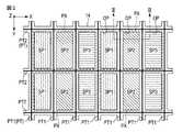
表示領域DAは、第1方向Xおよび第2方向Yにマトリクス状に配列された複数の画素PXを備えている。画素PXは、複数の副画素SPを備えている。一例では、画素PXは、赤色の副画素SP1、緑色の副画素SP2および青色の副画素SP3を備えている。なお、画素PXは、上記の3色の副画素の他に、白色などの他の色の副画素を加えた4個以上の副画素を備えてもよい。 The display area DA includes a plurality of pixels PX arranged in a matrix in the first direction X and the second direction Y. As shown in FIG. A pixel PX includes a plurality of sub-pixels SP. In one example, the pixel PX comprises a red sub-pixel SP1, a green sub-pixel SP2 and a blue sub-pixel SP3. The pixel PX may include four or more sub-pixels including sub-pixels of other colors such as white, in addition to the sub-pixels of the three colors described above.
副画素SPは、画素回路1と、画素回路1によって駆動される表示素子20とを備えている。画素回路1は、画素スイッチ2と、駆動トランジスタ3と、キャパシタ4とを備えている。画素スイッチ2および駆動トランジスタ3は、例えば薄膜トランジスタにより構成されたスイッチング素子である。 A sub-pixel SP includes a
画素スイッチ2において、ゲート電極は走査線GLに接続されている。画素スイッチ2のソース電極およびドレイン電極の一方は信号線SLに接続され、他方は駆動トランジスタ3のゲート電極およびキャパシタ4に接続されている。駆動トランジスタ3において、ソース電極およびドレイン電極の一方は電源線PLおよびキャパシタ4に接続され、他方は表示素子20のアノードに接続されている。表示素子20は、発光素子としての有機発光ダイオード(OLED)である。表示素子20のカソードは、共通電圧が印加された給電線FLに接続されている。なお、画素回路1の構成は図示した例に限らない。 The gate electrode of the
図2は、副画素SP(SP1,SP2,SP3)のレイアウトの一例を示す図である。ここでは、4個の画素PXに着目する。それぞれの画素PXにおいて、副画素SP1,SP2,SP3はこの順で第1方向Xに並んでいる。すなわち、表示領域DAにおいて、第2方向Yに並ぶ複数の副画素SP1により構成される列と、第2方向Yに並ぶ複数の副画素SP2により構成される列と、第2方向Yに並ぶ複数の副画素SP3により構成される列とが、第1方向Xにおいて交互に配置されている。 FIG. 2 is a diagram showing an example layout of the sub-pixels SP (SP1, SP2, SP3). Here, attention is focused on four pixels PX. In each pixel PX, the sub-pixels SP1, SP2 and SP3 are arranged in the first direction X in this order. That is, in the display area DA, a column formed by a plurality of sub-pixels SP1 arranged in the second direction Y, a column formed by a plurality of sub-pixels SP2 arranged in the second direction Y, and a plurality of sub-pixels SP2 arranged in the second direction Y are arranged alternately in the first direction X.
副画素SP1,SP2,SP3の境界には、リブ14が配置されている。図2の例において、リブ14は、第1方向Xに隣り合う副画素SPの間に位置する部分と、第2方向Yに隣り合う副画素SPの間に位置する部分とを有した格子状である。リブ14は、副画素SP1,SP2,SP3のそれぞれにおいて開口OPを形成する。
リブ14の上には、複数の隔壁PTが配置されている。図2の例において、複数の隔壁PTは、第2方向Yと平行な複数の隔壁PT1と、第1方向Xと平行な複数の隔壁PT2とを含む。 A plurality of partition walls PT are arranged on the
隔壁PT1は、第1方向Xに隣り合う副画素SP1,SP2の間、第1方向Xに隣り合う副画素SP2,SP3の間、および、第1方向Xに隣り合う副画素SP1,SP3の間にそれぞれ位置している。すなわち、隔壁PT1は、異なる色の副画素SPの境界に位置している。 The partition PT1 is located between the sub-pixels SP1 and SP2 adjacent in the first direction X, between the sub-pixels SP2 and SP3 adjacent in the first direction X, and between the sub-pixels SP1 and SP3 adjacent in the first direction X. are located respectively. That is, the partition PT1 is positioned at the boundary between the sub-pixels SP of different colors.
隔壁PT2は、第2方向Yに隣り合う2つの副画素SP1の間、第2方向Yに隣り合う2つの副画素SP2の間、および、第2方向Yに隣り合う2つの副画素SP3の間にそれぞれ位置している。すなわち、隔壁PT2は、同じ色の副画素SPの境界に位置している。なお、同じ色の副画素SPにおいては混色が生じないため、隔壁PT2が省略されてもよい。 The partition PT2 is located between two sub-pixels SP1 adjacent in the second direction Y, between two sub-pixels SP2 adjacent in the second direction Y, and between two sub-pixels SP3 adjacent in the second direction Y. are located respectively. That is, the partition wall PT2 is positioned at the boundary between the sub-pixels SP of the same color. Note that the partition wall PT2 may be omitted since color mixture does not occur in the sub-pixels SP of the same color.
図3は、図2のIII-III線に沿う表示装置DSPの概略的な断面図である。図3においては、主に副画素SP2の断面構造を示すが、副画素SP1,SP3も同様の断面構造を有している。なお、副画素SP2に配置される素子として駆動トランジスタ3および表示素子20を示し、その他の素子の図示を省略している。 FIG. 3 is a schematic cross-sectional view of the display device DSP along line III-III in FIG. Although FIG. 3 mainly shows the cross-sectional structure of the sub-pixel SP2, the sub-pixels SP1 and SP3 also have the same cross-sectional structure. Note that the driving
表示装置DSPは、上述の基材10、リブ14、隔壁PT1および給電線FLに加え、絶縁層11,12,13と、第1無機層IL1と、第2無機層IL2と、第3無機層IL3と、樹脂層RLとを備えている。 The display device DSP includes insulating
絶縁層11,12,13は、基材10の上において第3方向Zに積層されている。絶縁層11,12は、例えば無機材料で形成されている。絶縁層13は、例えば有機材料で形成されている。 The insulating layers 11 , 12 , 13 are laminated in the third direction Z on the
駆動トランジスタ3は、半導体層30と、電極31,32,33とを備えている。電極31は、ゲート電極に相当する。電極32,33の一方はソース電極に相当し、他方はドレイン電極に相当する。半導体層30は、基材10と絶縁層11の間に配置されている。電極31は、絶縁層11,12の間に配置されている。電極32,33は、絶縁層12,13の間に配置され、絶縁層11,12を貫通するコンタクトホールを通じて半導体層30に接触している。 The
表示素子20は、第1電極E1と、有機層ORと、第2電極E2とを備えている。第1電極E1は、副画素SP毎に配置された電極であり、画素電極、下部電極またはアノードと称される場合がある。第2電極E2は、複数の副画素SPに対して共通に配置された電極であり、共通電極、上部電極またはカソードと称される場合がある。 The
リブ14は、絶縁層13の上に配置されている。リブ14は、有機材料で形成することができる。第1電極E1は、絶縁層13の上に配置され、開口OPと重なっている。第1電極E1の周縁部は、リブ14により覆われている。第1電極E1は、絶縁層13を貫通するコンタクトホールを通じて電極33と電気的に接続されている。第1電極E1は、金属材料で形成されている。ただし、第1電極E1は、インジウム錫酸化物(ITO)やインジウム亜鉛酸化物(IZO)などの透明導電材料で形成されてもよいし、透明導電材料と金属材料の積層体であってもよい。 The
有機層ORは、開口OPを通じて第1電極E1に接触している。有機層ORの一部は、リブ14の上に位置している。第2電極E2は、有機層ORを覆っている。第2電極E2は、例えば金属材料で形成されている。ただし、第2電極E2は、ITOやIZOなどの透明導電材料で形成されてもよい。 The organic layer OR is in contact with the first electrode E1 through the opening OP. A portion of the organic layer OR is located above the
隔壁PT1は、リブ14の上に配置されている。図2に示した隔壁PT2もリブ14の上に配置されている。隔壁PT1,PT2は、例えば有機材料で形成されている。 The partition wall PT1 is arranged on the
給電線FLは、金属材料で形成され、リブ14の上に配置されている。図3の例においては、リブ14の上に2本の給電線FLが配置され、これら給電線FLの間に隔壁PT1が配置されている。給電線FLは、例えば図2に示した隔壁PT2の下を通り、第2方向Yに延びている。給電線FLは、隔壁PT1の直下に配置されてもよい。また、隔壁PT2に沿って第1方向Xに延びる給電線FLがさらに配置されてもよい。 The feeder line FL is made of a metal material and arranged on the
第1無機層IL1は、第2電極E2、リブ14および隔壁PT1,PT2を覆っている。第2無機層IL2は、第1無機層IL1を覆っている。樹脂層RLは、第2無機層IL2を覆っている。樹脂層RLは、例えば有機材料(樹脂)によって形成されている。樹脂層RLは、絶縁層11,12,13、リブ14、第1無機層IL1、第2無機層IL2、第3無機層IL3および隔壁PT1,PT2よりも厚く、リブ14や隔壁PT1,PT2により生じる凹凸を平坦化している。第3無機層IL3は、樹脂層RLを覆っている。 The first inorganic layer IL1 covers the second electrodes E2,
第1無機層IL1、第2無機層IL2および第3無機層IL3は、例えばシリコン酸化物(SiOx)、シリコン窒化物(SiNx)、シリコン酸窒化物(SiONx)、金属、金属酸化物などの無機材料で形成されている。第1無機層IL1および第2無機層IL2は、両者の密着性の観点からは、同じ無機材料で形成されることが好ましい。また、例えば第1無機層IL1および第2無機層IL2の一方がシリコン酸化物であり、他方がシリコン窒化物である場合のように、第1無機層IL1および第2無機層IL2の双方がシリコン系の無機材料で形成されてもよい。さらに、第1無機層IL1および第2無機層IL2は、シリコン系以外の同系統の無機材料で形成されてもよい。これらの場合であっても、第1無機層IL1および第2無機層IL2の密着性を向上させることができる。第3無機層IL3に関しても、第1無機層IL1および第2無機層IL2と同じ無機材料で形成されてもよいし、第1無機層IL1および第2無機層IL2と同系統の無機材料で形成されてもよい。 The first inorganic layer IL1, the second inorganic layer IL2, and the third inorganic layer IL3 are made of an inorganic material such as silicon oxide (SiOx), silicon nitride (SiNx), silicon oxynitride (SiONx), metal, or metal oxide. made of material. The first inorganic layer IL1 and the second inorganic layer IL2 are preferably made of the same inorganic material from the viewpoint of adhesion between them. Further, both the first inorganic layer IL1 and the second inorganic layer IL2 are made of silicon, for example, when one of the first inorganic layer IL1 and the second inorganic layer IL2 is made of silicon oxide and the other is made of silicon nitride. It may be formed of an inorganic material of the system. Furthermore, the first inorganic layer IL1 and the second inorganic layer IL2 may be formed of a similar inorganic material other than a silicon-based material. Even in these cases, the adhesion between the first inorganic layer IL1 and the second inorganic layer IL2 can be improved. The third inorganic layer IL3 may also be made of the same inorganic material as the first inorganic layer IL1 and the second inorganic layer IL2, or may be made of the same inorganic material as the first inorganic layer IL1 and the second inorganic layer IL2. may be
本実施形態においては、後述するように第1無機層IL1および第2無機層IL2を異なる成膜条件で蒸着により形成する。そのため、仮に第1無機層IL1および第2無機層IL2を同じ材料で形成した場合であっても、第1無機層IL1および第2無機層IL2の膜密度や組成比が異なり得る。第1無機層IL1、第2無機層IL2、樹脂層RLおよび第3無機層IL3は、有機層ORを水分などから保護する封止層として機能する。 In this embodiment, the first inorganic layer IL1 and the second inorganic layer IL2 are formed by vapor deposition under different film forming conditions, as will be described later. Therefore, even if the first inorganic layer IL1 and the second inorganic layer IL2 are made of the same material, the film densities and composition ratios of the first inorganic layer IL1 and the second inorganic layer IL2 may differ. The first inorganic layer IL1, the second inorganic layer IL2, the resin layer RL, and the third inorganic layer IL3 function as sealing layers that protect the organic layer OR from moisture and the like.
図4は、有機層ORに適用し得る層構成の一例を示す断面図である。例えば、有機層ORは、第1電極E1から第2電極E2に向けて順に積層された第1機能層F1、発光層ELおよび第2機能層F2を含んでいる。 FIG. 4 is a cross-sectional view showing an example of a layer structure applicable to the organic layer OR. For example, the organic layer OR includes a first functional layer F1, a light-emitting layer EL, and a second functional layer F2 which are laminated in order from the first electrode E1 toward the second electrode E2.
第1電極E1の電位が第2電極E2の電位よりも相対的に高い場合、第1電極E1がアノードに相当し、第2電極E2がカソードに相当する。また、第2電極E2の電位が第1電極E1の電位よりも相対的に高い場合、第2電極E2がアノードに相当し、第1電極E1がカソードに相当する。 When the potential of the first electrode E1 is relatively higher than the potential of the second electrode E2, the first electrode E1 corresponds to the anode and the second electrode E2 corresponds to the cathode. Further, when the potential of the second electrode E2 is relatively higher than the potential of the first electrode E1, the second electrode E2 corresponds to the anode and the first electrode E1 corresponds to the cathode.
一例として、第1電極E1がアノードに相当する場合、第1機能層F1は正孔注入層、正孔輸送層および電子ブロッキング層の少なくとも1つを含み、第2機能層F2は電子輸送層、電子注入層および正孔ブロッキング層の少なくとも1つを含む。 As an example, when the first electrode E1 corresponds to an anode, the first functional layer F1 includes at least one of a hole injection layer, a hole transport layer and an electron blocking layer, and the second functional layer F2 is an electron transport layer, It includes at least one of an electron injection layer and a hole blocking layer.
第1電極E1と第2電極E2の間に電位差が形成されると、発光層ELが発光する。本実施形態においては、副画素SP1,SP2,SP3の有機層ORに含まれる発光層ELがいずれも同一色(例えば白色)の光を放つ場合を想定する。この場合において、例えば樹脂層RLの上方に副画素SP1,SP2,SP3の色に応じたカラーフィルタが配置されてもよい。また、発光層ELが放つ光により励起して副画素SP1,SP2,SP3に応じた色の光を生成する量子ドットを含んだ層が副画素SP1,SP2,SP3に配置されてもよい。なお、副画素SP1,SP2,SP3の発光層ELは、それぞれ副画素SP1,SP2,SP3に対応する色を放つものであってもよい。 When a potential difference is formed between the first electrode E1 and the second electrode E2, the light emitting layer EL emits light. In this embodiment, it is assumed that the light-emitting layers EL included in the organic layers OR of the sub-pixels SP1, SP2, and SP3 all emit light of the same color (for example, white). In this case, for example, color filters corresponding to the colors of the sub-pixels SP1, SP2, and SP3 may be arranged above the resin layer RL. A layer containing quantum dots that are excited by the light emitted by the light-emitting layer EL to generate light of a color corresponding to the sub-pixels SP1, SP2, SP3 may be arranged in the sub-pixels SP1, SP2, SP3. The light-emitting layers EL of the sub-pixels SP1, SP2, SP3 may emit colors corresponding to the sub-pixels SP1, SP2, SP3, respectively.
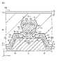
図5は、図3において副画素SP1,SP2の間に位置する隔壁PT1の近傍を拡大した概略的な断面図である。隔壁PT1は、第1部分P1と、第1部分P1の下方に位置する第2部分P2とを有している。図5の例においては、第2部分P2がリブ14の上面14aに接触している。 FIG. 5 is a schematic cross-sectional view enlarging the vicinity of the partition wall PT1 located between the sub-pixels SP1 and SP2 in FIG. The partition PT1 has a first portion P1 and a second portion P2 positioned below the first portion P1. In the example of FIG. 5, the second portion P2 is in contact with the
第1部分P1は、第1幅W1aを有している。第2部分P2は、第2幅W2aを有している。第2幅W2aは、第1幅W1よりも小さい(W1a>W2a)。 The first portion P1 has a first width W1a. The second portion P2 has a second width W2a. The second width W2a is smaller than the first width W1 (W1a>W2a).
図5の例において、第1部分P1の一対の側面SF1は、これら側面SF1の間の距離が第1部分P1の上端から下端に向けて小さくなるように傾斜している。すなわち、第1部分P1の幅は、第3方向Zにおいて一定ではない。第1幅W1aは、第1部分P1の最大幅に相当し、図示した例においては第1部分P1の上端の幅である。なお、一対の側面SF1は、第3方向Zと平行であってもよい。また、一対の側面SF1は、これら側面SF1の間の距離が第1部分P1の上端から下端に向けて大きくなるように傾斜していてもよい。図5の例において、第2部分P2の一対の側面SF2は、第3方向Zと平行である。ただし、一対の側面SF2は、第3方向Zに対して傾斜していてもよい。 In the example of FIG. 5, the pair of side surfaces SF1 of the first portion P1 are inclined such that the distance between the side surfaces SF1 decreases from the upper end to the lower end of the first portion P1. That is, the width of the first portion P1 is not constant in the third direction Z. The first width W1a corresponds to the maximum width of the first portion P1, and is the width of the upper end of the first portion P1 in the illustrated example. Note that the pair of side surfaces SF1 may be parallel to the third direction Z. Also, the pair of side surfaces SF1 may be inclined such that the distance between the side surfaces SF1 increases from the upper end to the lower end of the first portion P1. In the example of FIG. 5, the pair of side surfaces SF2 of the second portion P2 are parallel to the third direction Z. As shown in FIG. However, the pair of side surfaces SF2 may be inclined with respect to the third direction Z.
第1部分P1は、側面SF1と側面SF2を繋ぐ一対の下面BFを有している。これら下面BFは、リブ14の上面14aと対向している。このような形状の第1部分P1と第2部分P2を有する隔壁PT1の形状は、例えばオーバーハング形状と呼ぶことができる。隔壁PT1の形状は、図5に示す例に限られない。例えば、隔壁PT1は、下面BFに相当する部分を有さない形状(逆テーパー形状)を有してもよい。 The first portion P1 has a pair of lower surfaces BF connecting the side surface SF1 and the side surface SF2. These lower surfaces BF are opposed to
隔壁PT1(第1部分P1)の上には、有機層ORaと、有機層ORaを覆う導電層E2aとが配置されている。有機層ORaは、有機層ORと同じ材料で形成されている。導電層E2aは、第2電極E2と同じ材料で形成されている。有機層ORaは、副画素SP1,SP2に配置された有機層ORと離間している。導電層E2aは、副画素SP1,SP2に配置された第2電極E2と離間している。 An organic layer ORa and a conductive layer E2a covering the organic layer ORa are arranged on the partition PT1 (first portion P1). The organic layer ORa is made of the same material as the organic layer OR. The conductive layer E2a is made of the same material as the second electrode E2. The organic layer ORa is separated from the organic layers OR arranged in the sub-pixels SP1 and SP2. The conductive layer E2a is separated from the second electrodes E2 arranged on the sub-pixels SP1 and SP2.
有機層ORおよび第2電極E2は、例えば真空蒸着により表示領域DAの全面に形成される。このとき、隔壁PT1の上面に蒸着源からの材料が付着することにより、有機層ORaおよび導電層E2aが形成される。一方、側面SF1,SF2には蒸着源からの材料が付着しにくい。これにより、有機層ORと有機層ORaが分断され、第2電極E2と導電層E2aが分断される。 The organic layer OR and the second electrode E2 are formed on the entire surface of the display area DA by vacuum deposition, for example. At this time, the organic layer ORa and the conductive layer E2a are formed by depositing the material from the vapor deposition source on the upper surface of the partition wall PT1. On the other hand, it is difficult for the material from the deposition source to adhere to the side surfaces SF1 and SF2. As a result, the organic layer OR and the organic layer ORa are separated, and the second electrode E2 and the conductive layer E2a are separated.
有機層ORは、リブ14の上面14aにおいて第1端部ED1を有している。第2電極E2は、上面14aにおいて第2端部ED2を有している。第1端部ED1および第2端部ED2は、いずれも第2部分P2と離間している。第2端部ED2は、第1方向Xにおいて第1端部ED1と第2部分P2の間に位置している。第1端部ED1は、第2電極E2により覆われている。 The organic layer OR has a first end ED<b>1 on the
給電線FLは、上面14aにおいて第1端部ED1と第2部分P2の間に位置している。第2電極E2は、給電線FLと接触している。図5の例においては、給電線FLの全体が第2電極E2により覆われており、第2端部ED2が給電線FLと第2部分P2の間に位置している。ただし、給電線FLの一部が第2電極E2により覆われていなくてもよい。 Feeder line FL is positioned between first end ED1 and second portion P2 on
第1無機層IL1は、副画素SP1,SP2の第2電極E2、上面14a、一対の側面SF1、一対の側面SF2、一対の下面BFおよび導電層E2aを連続的に覆っている。第2無機層IL2は、第1無機層IL1の上面を連続的に覆っている。 The first inorganic layer IL1 continuously covers the second electrodes E2 of the sub-pixels SP1 and SP2, the
なお、図5においては副画素SP1,SP2の境界付近の構造を示したが、副画素SP2,SP3の境界付近や副画素SP1,SP3の境界付近にも同様の構造を適用できる。図2に示した隔壁PT2には隔壁PT1と同様の形状を適用できる。図5に示した構造は、第2方向Yに並ぶ2つの副画素SP1の境界付近、第2方向Yに並ぶ2つの副画素SP2の境界付近、第2方向Yに並ぶ2つの副画素SP3の境界付近の断面構造にも適用できる。 Although the structure near the boundary between the subpixels SP1 and SP2 is shown in FIG. 5, the same structure can be applied to the boundary between the subpixels SP2 and SP3 and the boundary between the subpixels SP1 and SP3. A shape similar to that of the partition PT1 can be applied to the partition PT2 shown in FIG. The structure shown in FIG. It can also be applied to cross-sectional structures near boundaries.
第1無機層IL1は、第2電極E2が形成された後に、例えば化学蒸着法(CVD)などの蒸着により形成される。第1無機層IL1を蒸着により形成するときに、大きな角度をなす2つの面で構成される角の近傍においては、一方の面から無機層が成長するとともに、他方の面からも無機層が成長してくる。これら無機層が接近すると、その間の部分へのガスの流入が抑制され、クレバス状のボイド(隙間)やシームが形成されることがある。ボイドには樹脂層RLが入り込みにくいため、ボイド内に大気が残留し得る。 The first inorganic layer IL1 is formed by vapor deposition such as chemical vapor deposition (CVD) after the second electrode E2 is formed. When the first inorganic layer IL1 is formed by vapor deposition, in the vicinity of the corner formed by two surfaces forming a large angle, the inorganic layer grows from one surface and the inorganic layer also grows from the other surface. come. When these inorganic layers approach each other, the inflow of gas into the portion between them is suppressed, and crevice-like voids (clearances) and seams may be formed. Since it is difficult for the resin layer RL to enter the voids, air may remain in the voids.
図5の例においては、側面SF2と下面BFの角付近においてボイドVが形成されている。このボイドVに代えて、側面SF2と下面BFの角付近にシームが形成される可能性もある。また、第2部分P2の根本付近にボイドやシームが形成される可能性もある。 In the example of FIG. 5, a void V is formed near the corner between the side surface SF2 and the bottom surface BF. Instead of this void V, a seam may be formed near the corner between the side surface SF2 and the bottom surface BF. Also, voids and seams may be formed near the base of the second portion P2.
従来、有機エレクトロルミネッセンス表示装置の封止層としては、下層の無機層、樹脂層、上層の無機層が順に積層された3層封止構造が一般的である。このような3層封止構造を本実施形態のように隔壁PT1,PT2を有する表示装置に適用すると、下層の無機層にボイドやシームが生じた場合、表示素子への水分浸入を十分に抑制できない可能性がある。すなわち、例えば樹脂層が当初より水分を含んでいたとしたら、この水分がボイドやシームを通じて表示素子に到達し得る。また、上層の無機層にクラックが生じた場合、このクラック、樹脂層、下層の無機層のボイドやシームを順に通って表示素子に水分が浸入し得る。水分が表示素子(特に有機層OR)に到達すると、表示素子の輝度低下(ダークスポットの発生)などの表示不良の一因となり得る。 Conventionally, as a sealing layer of an organic electroluminescence display device, a three-layer sealing structure in which a lower inorganic layer, a resin layer, and an upper inorganic layer are laminated in this order is generally used. When such a three-layer sealing structure is applied to a display device having partition walls PT1 and PT2 as in the present embodiment, even if voids or seams occur in the lower inorganic layer, penetration of moisture into the display element can be sufficiently suppressed. may not be possible. That is, for example, if the resin layer contains moisture from the beginning, this moisture may reach the display element through voids and seams. Further, when cracks occur in the upper inorganic layer, moisture may enter the display element through the cracks, the resin layer, and the voids and seams of the lower inorganic layer in this order. When moisture reaches the display element (especially the organic layer OR), it may cause display defects such as a decrease in luminance of the display element (occurrence of dark spots).
これに対し、本実施形態においては第1無機層IL1の上に第2無機層IL2が積層されている。そのため、第1無機層IL1にボイドやシームが発生した場合であっても、これらボイドやシームは第2無機層IL2により覆われるため、表示素子20に水分が浸入しにくい。これにより、表示装置DSPの表示品位を向上させることが可能となる。 In contrast, in the present embodiment, the second inorganic layer IL2 is laminated on the first inorganic layer IL1. Therefore, even if voids and seams are generated in the first inorganic layer IL1, the voids and seams are covered with the second inorganic layer IL2, so that moisture does not easily enter the
第2無機層IL2は、第1無機層IL1と同じく蒸着により形成される。第2無機層IL2は、第1無機層IL1においてボイドやシームが発生し得る箇所も連続的に覆う必要があることから、第1無機層IL1の成膜条件よりも回り込み特性が良好な成膜条件で形成されることが好ましい。 The second inorganic layer IL2 is formed by vapor deposition like the first inorganic layer IL1. Since it is necessary for the second inorganic layer IL2 to continuously cover locations where voids and seams may occur in the first inorganic layer IL1, the film formation conditions are such that the wraparound characteristic is better than the film formation conditions for the first inorganic layer IL1. It is preferably formed under conditions.
良好な回り込み特性は、蒸着装置の構造を工夫することによっても実現できる。例えば、蒸着装置が備えるシャワープレートの形状を調整してもよい。具体的には、第2無機層IL2の成膜時に使用するシャワープレートに設けられた複数の開口を、ワークに近づくに連れて径が大きくなるテーパー形状としてもよい。 Good wraparound characteristics can also be realized by devising the structure of the vapor deposition apparatus. For example, the shape of the shower plate included in the vapor deposition apparatus may be adjusted. Specifically, the plurality of openings provided in the shower plate used when forming the second inorganic layer IL2 may have a tapered shape in which the diameter increases toward the workpiece.
また、ホローカソード方式の蒸着装置を利用する場合、アノードの開口をカソードの開口に対して大きくしてもよいし、アノードの開口をワークに近づくに連れて径が大きくなるテーパー形状としてもよい。 When a hollow cathode vapor deposition apparatus is used, the anode opening may be made larger than the cathode opening, or the anode opening may have a tapered shape in which the diameter increases as it approaches the workpiece.
第1無機層IL1は、各副画素SP1,SP2,SP3やこれらの境界において全体的に下層への水分浸入を良好に抑制する必要があることから、ある程度の厚さを有する必要がある。これに対し、第2無機層IL2は、ボイドやシームが生じないように、遅い成長速度で緻密に形成する必要がある。 The first inorganic layer IL1 needs to have a certain degree of thickness because it is necessary to satisfactorily suppress moisture intrusion into the underlying layer as a whole at each of the sub-pixels SP1, SP2, SP3 and their boundaries. On the other hand, the second inorganic layer IL2 needs to be grown densely at a slow growth rate so as not to generate voids or seams.
このような観点から、本実施形態においては、第1無機層IL1の厚さt1が第2無機層IL2の厚さt2よりも大きい。すなわち、第2無機層IL2は第1無機層IL1よりも薄く形成されている。第3無機層IL3の厚さt3は、例えば厚さt1と同等である。一例として、厚さt2は、厚さt1の1/2以下である。厚さt2は、厚さt1の1/10以下であってもよい。 From this point of view, in the present embodiment, the thickness t1 of the first inorganic layer IL1 is larger than the thickness t2 of the second inorganic layer IL2. That is, the second inorganic layer IL2 is formed thinner than the first inorganic layer IL1. The thickness t3 of the third inorganic layer IL3 is, for example, equivalent to the thickness t1. As an example, the thickness t2 is less than half the thickness t1. The thickness t2 may be 1/10 or less of the thickness t1.
なお、側面SF2と下面BFの角付近や第2部分P2の根本付近の凹凸は、第1無機層IL1により緩和される。そのため、第2無機層IL2にはこれら角付近や根本付近においてボイドやシームが生じにくい。 In addition, unevenness near the corner between the side surface SF2 and the bottom surface BF and near the root of the second portion P2 is alleviated by the first inorganic layer IL1. Therefore, voids and seams are less likely to occur in the vicinity of these corners and roots of the second inorganic layer IL2.
なお、第1無機層IL1と第2無機層IL2を別々のプロセスにて成膜する場合、第1無機層IL1と第2無機層IL2の間には明確な界面が形成される。一方、第1無機層IL1を成膜するプロセスの終盤から徐々に成膜条件を変えて第2絶縁層IL2を成膜することもできる。この場合には、第1無機層IL1と第2無機層IL2の境界がグラデーションとなり、両者の間に明確な界面が形成されない。
ここでは図5のように隔壁PT1を含む断面に基づき本実施形態が奏する効果の一例を説明したが、隔壁PT2付近においても同様の効果を得ることができる。Note that when the first inorganic layer IL1 and the second inorganic layer IL2 are formed by separate processes, a clear interface is formed between the first inorganic layer IL1 and the second inorganic layer IL2. On the other hand, it is also possible to form the second insulating layer IL2 by gradually changing the film formation conditions from the final stage of the process of forming the first inorganic layer IL1. In this case, the boundary between the first inorganic layer IL1 and the second inorganic layer IL2 becomes a gradation, and a clear interface is not formed between them.
Here, an example of the effects of the present embodiment has been described based on the cross section including the partition wall PT1 as shown in FIG. 5, but similar effects can be obtained in the vicinity of the partition wall PT2.
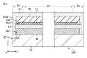
図6は、図1におけるVI-VI線に沿う表示装置DSPの概略的な断面図である。この図においては、基材10の上に配置される絶縁層11,12,13、リブ14、隔壁PT1,PT2、画素回路1および表示素子20等の要素を回路層40として簡略化している。 FIG. 6 is a schematic cross-sectional view of the display device DSP along line VI-VI in FIG. In this figure, elements such as insulating
回路層40、第1無機層IL1、第2無機層IL2、第3無機層IL3および樹脂層RLは、表示領域DAの全体に形成されるとともに、周辺領域SAにも及んでいる。すなわち、回路層40の端部ED40、第1無機層IL1の端部EDi1、第2無機層IL2の端部EDi2、第3無機層IL3の端部EDi3および樹脂層RLの端部EDrは、いずれも周辺領域SAに位置している。 The
図6の例においては、端部EDi1,EDi2,EDi3および基材10の端部ED10が揃っている。一方で、端部ED40,EDrが端部EDi1,EDi2,EDi3よりも表示領域DA寄りに位置している。端部ED10は、端部EDi1,EDi2,EDi3より突出してもよい。すなわち、端部EDi1,EDi2,EDi3は、周辺領域SAにおいて端部ED10と端部EDr,ED40の間に位置してもよい。 In the example of FIG. 6, the ends EDi1, EDi2, EDi3 and the end ED10 of the
第1無機層IL1は、周辺領域SAにおいて基材10に接触している。第3無機層IL3は、周辺領域SAにおいて第2無機層IL2に接触している。回路層40の端部ED40は、第1無機層IL1により覆われている。樹脂層RLの端部EDrは、第3無機層IL3により覆われている。 The first inorganic layer IL1 is in contact with the
このような構成であれば、表示装置DSPの周縁部から回路層40や樹脂層RLへの水分浸入を第1無機層IL1、第2無機層IL2および第3無機層IL3により良好に抑制できる。 With such a configuration, the first inorganic layer IL1, the second inorganic layer IL2, and the third inorganic layer IL3 can satisfactorily suppress moisture from entering the
図7は、表示装置DSPに適用し得る他の例を示す概略的な断面図である。この例では、第2無機層IL2の端部EDi2が第3無機層IL3の端部EDi3よりも表示領域DA寄りに位置している。端部EDi2は、第3無機層IL3により覆われている。第3無機層IL3は、周辺領域SAにおいて第1無機層IL1と接触している。図7の例においては端部ED10,EDi1,EDi3が揃っているが、端部ED10は端部EDi1,EDi3より突出してもよい。すなわち、端部EDi1,EDi3は、周辺領域SAにおいて端部ED10と端部EDi2,EDr,ED40の間に位置してもよい。 FIG. 7 is a schematic cross-sectional view showing another example applicable to the display device DSP. In this example, the end EDi2 of the second inorganic layer IL2 is located closer to the display area DA than the end EDi3 of the third inorganic layer IL3. The end EDi2 is covered with a third inorganic layer IL3. The third inorganic layer IL3 is in contact with the first inorganic layer IL1 in the peripheral area SA. Although the ends ED10, EDi1, and EDi3 are aligned in the example of FIG. 7, the end ED10 may protrude from the ends EDi1 and EDi3. That is, ends EDi1 and EDi3 may be positioned between end ED10 and ends EDi2, EDr and ED40 in peripheral area SA.
例えば、第3無機層IL3を第1無機層IL1と同様の成膜条件と材料で形成した場合、第3無機層IL3は第2無機層IL2に比べ第1無機層IL1に対する高い密着性を発揮し得る。このような場合、図7のように第3無機層IL3と第1無機層IL1が周辺領域SAにおいて接触していれば、回路層40や樹脂層RLへの水分浸入を良好に抑制できる。 For example, when the third inorganic layer IL3 is formed using the same deposition conditions and materials as those of the first inorganic layer IL1, the third inorganic layer IL3 exhibits higher adhesion to the first inorganic layer IL1 than the second inorganic layer IL2. can. In such a case, if the third inorganic layer IL3 and the first inorganic layer IL1 are in contact with each other in the peripheral region SA as shown in FIG. 7, it is possible to satisfactorily prevent moisture from entering the
図8は、表示装置DSPに適用し得るさらに他の例を示す概略的な断面図である。この例では、第1無機層IL1の端部EDi1および第2無機層IL2の端部EDi2が、第3無機層IL3の端部EDi3よりも表示領域DA寄りに位置している。端部EDi1,EDi2は、第3無機層IL3により覆われている。第3無機層IL3は、周辺領域SAにおいて基材10と接触している。図8の例においては端部ED10,EDi3が揃っているが、端部ED10は端部EDi3より突出してもよい。すなわち、端部EDi3は、周辺領域SAにおいて端部ED10と端部EDi1,EDi2,EDr,ED40の間に位置してもよい。 FIG. 8 is a schematic cross-sectional view showing still another example applicable to the display device DSP. In this example, the edge EDi1 of the first inorganic layer IL1 and the edge EDi2 of the second inorganic layer IL2 are positioned closer to the display area DA than the edge EDi3 of the third inorganic layer IL3. The ends EDi1 and EDi2 are covered with a third inorganic layer IL3. The third inorganic layer IL3 is in contact with the
図8のような構成であれば、回路層40の端部ED40が第1無機層IL1および第3無機層IL3によって2重に覆われる。また、表示装置DSPの周縁部においては、回路層40に向けた水分浸入の経路が基材10と第3無機層IL3の境界に限られる。これらにより、回路層40への水分浸入を良好に抑制できる。 With the configuration as shown in FIG. 8, the end portion ED40 of the
図9は、表示装置DSPに適用し得るさらに他の例を示す概略的な断面図である。この例では、第2無機層IL2の端部EDi2が樹脂層RLの端部EDrよりも表示領域DA寄りに位置している。その他の構造は、図8の例と同様である。図9の例においては端部ED10,EDi3が揃っているが、端部ED10は端部EDi3より突出してもよい。すなわち、端部EDi3は、周辺領域SAにおいて端部ED10と端部EDi1,EDi2,EDr,ED40の間に位置してもよい。 FIG. 9 is a schematic cross-sectional view showing still another example applicable to the display device DSP. In this example, the end EDi2 of the second inorganic layer IL2 is positioned closer to the display area DA than the end EDr of the resin layer RL. Other structures are the same as in the example of FIG. Although the ends ED10 and EDi3 are aligned in the example of FIG. 9, the end ED10 may protrude from the end EDi3. That is, end EDi3 may be located between end ED10 and ends EDi1, EDi2, EDr, and ED40 in peripheral area SA.
なお、図6乃至図9においては第1方向Xに沿う表示装置DSPの断面を示したが、第2方向Yに沿う表示装置DSPの断面にも図6乃至図9と同様の構造を適用できる。 Although FIGS. 6 to 9 show the cross section of the display device DSP along the first direction X, the same structure as that of FIGS. 6 to 9 can be applied to the cross section of the display device DSP along the second direction Y. .
以上説明した本実施形態によれば、第1無機層IL1にボイドやシームが形成された場合であっても、これらボイドやシームを通じた水分浸入を抑制し、表示装置DSPの表示品位を高めることができる。 According to the present embodiment described above, even if voids or seams are formed in the first inorganic layer IL1, it is possible to suppress the infiltration of moisture through these voids or seams, thereby enhancing the display quality of the display device DSP. can be done.
[第2実施形態]
第2実施形態について説明する。本実施形態において特に言及しない構成は第1実施形態と同様である。[Second embodiment]
A second embodiment will be described. Configurations not particularly mentioned in this embodiment are the same as those in the first embodiment.
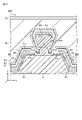
図10は、第2実施形態に係る表示装置DSPの一部の概略的な断面図である。図10においては、図5と同じく副画素SP1,SP2の間に位置する隔壁PT1の近傍を拡大して示している。 FIG. 10 is a schematic cross-sectional view of part of the display device DSP according to the second embodiment. 10, similarly to FIG. 5, the vicinity of the partition wall PT1 located between the sub-pixels SP1 and SP2 is shown enlarged.
本実施形態において、表示装置DSPは、第2無機層IL2と樹脂層RLの間に位置する第4無機層IL4をさらに備えている。第4無機層IL4は、第2無機層IL2を全体的に覆っている。樹脂層RLは、第4無機層IL4を全体的に覆っている。第1無機層IL1、第2無機層IL2、第3無機層IL3、第4無機層IL4および樹脂層RLは、本実施形態における封止層を構成する。 In this embodiment, the display device DSP further includes a fourth inorganic layer IL4 located between the second inorganic layer IL2 and the resin layer RL. The fourth inorganic layer IL4 entirely covers the second inorganic layer IL2. The resin layer RL entirely covers the fourth inorganic layer IL4. The first inorganic layer IL1, the second inorganic layer IL2, the third inorganic layer IL3, the fourth inorganic layer IL4, and the resin layer RL constitute the sealing layer in this embodiment.
第4無機層IL4は、例えばシリコン酸化物(SiOx)、シリコン窒化物(SiNx)、シリコン酸窒化物(SiONx)、金属、金属酸化物などの無機材料で形成されている。第2無機層IL2に加えて第4無機層IL4を設けることにより、第1無機層IL1に形成され得るボイドVやシームを通じた表示素子20への水分浸入をより良好に抑制することができる。 The fourth inorganic layer IL4 is made of an inorganic material such as silicon oxide (SiOx), silicon nitride (SiNx), silicon oxynitride (SiONx), metal, or metal oxide. By providing the fourth inorganic layer IL4 in addition to the second inorganic layer IL2, it is possible to better suppress moisture from entering the
第4無機層IL4を第1無機層IL1と同じ材料かつ同じ成膜条件で形成すると、第1無機層IL1および第4無機層IL4の同じ位置にボイドやシームが形成され得る。そこで、第4無機層IL4は、第1無機層IL1と異なる材料または異なる成膜条件で形成されることが好ましい。 If the fourth inorganic layer IL4 is formed from the same material and under the same deposition conditions as the first inorganic layer IL1, voids and seams may be formed at the same positions in the first inorganic layer IL1 and the fourth inorganic layer IL4. Therefore, the fourth inorganic layer IL4 is preferably formed using a material different from that of the first inorganic layer IL1 or under different film forming conditions.
例えば、第4無機層IL4は、第2無機層IL2のように回り込み特性が良好な成膜条件で形成されてもよい。また、例えば第1無機層IL1がシリコン酸化物、シリコン窒化物またはシリコン酸窒化物により形成され、第4無機層IL4が金属または金属酸化物により形成されてもよい。 For example, the fourth inorganic layer IL4 may be formed under film formation conditions with good wraparound characteristics like the second inorganic layer IL2. Alternatively, for example, the first inorganic layer IL1 may be made of silicon oxide, silicon nitride or silicon oxynitride, and the fourth inorganic layer IL4 may be made of metal or metal oxide.
図11は、本実施形態に係る表示装置DSPの全体の概略的な断面図である。この図においては、図6と同じく、基材10の上に配置される絶縁層11,12,13、リブ14、隔壁PT1,PT2、画素回路1および表示素子20等の要素を回路層40として簡略化している。 FIG. 11 is a schematic cross-sectional view of the entire display device DSP according to this embodiment. In this figure, elements such as insulating
回路層40、第1無機層IL1、第2無機層IL2、第3無機層IL3、第4無機層IL4および樹脂層RLは、表示領域DAの全体に形成されるとともに、周辺領域SAにも及んでいる。すなわち、回路層40の端部ED40、第1無機層IL1の端部EDi1、第2無機層IL2の端部EDi2、第3無機層IL3の端部EDi3、第4無機層IL4の端部EDi4および樹脂層RLの端部EDrは、いずれも周辺領域SAに位置している。 The
図11の例においては、端部EDi1,EDi3,EDi4および基材10の端部ED10が揃っている。一方で、端部ED40,EDr,EDi2が端部EDi1,EDi3,EDi4よりも表示領域DA寄りに位置している。端部ED10は、端部EDi1,EDi3,EDi4より突出してもよい。すなわち、端部EDi1,EDi3,EDi4は、周辺領域SAにおいて端部ED10と端部EDi2,EDr,ED40の間に位置してもよい。 In the example of FIG. 11, the ends EDi1, EDi3, EDi4 and the end ED10 of the
第1無機層IL1は、周辺領域SAにおいて基材10に接触している。第3無機層IL3は、周辺領域SAにおいて第4無機層IL4に接触している。第4無機層IL4は、周辺領域SAにおいて第1無機層IL1に接触している。回路層40の端部ED40は、第1無機層IL1により覆われている。樹脂層RLの端部EDrは、第3無機層IL3により覆われている。第2無機層IL2の端部EDi2は、第4無機層IL4により覆われている。 The first inorganic layer IL1 is in contact with the
このように第4無機層IL4が周辺領域SAにおいて第1無機層IL1および第3無機層IL3と接触した構成であれば、これら無機層IL1,IL3,IL4により、表示装置DSPの周縁部から表示領域DAに向けた水分浸入を良好に抑制できる。 With such a configuration in which the fourth inorganic layer IL4 is in contact with the first inorganic layer IL1 and the third inorganic layer IL3 in the peripheral area SA, these inorganic layers IL1, IL3, and IL4 provide a display from the peripheral portion of the display device DSP. It is possible to satisfactorily suppress moisture intrusion toward the area DA.
図12は、本実施形態に係る表示装置DSPに適用し得る他の例を示す概略的な断面図である。この例では、第1無機層IL1の端部EDi1が第4無機層IL4の端部EDi4よりも表示領域DA寄りに位置している。端部EDi1は、第4無機層IL4により覆われている。第4無機層IL4は、周辺領域SAにおいて基材10と接触している。図12の例においては端部ED10,EDi3,EDi4が揃っているが、端部ED10は端部EDi3,EDi4より突出してもよい。すなわち、端部EDi3,EDi4は、周辺領域SAにおいて端部ED10と端部EDi1,EDi2,EDr,ED40の間に位置してもよい。 FIG. 12 is a schematic cross-sectional view showing another example applicable to the display device DSP according to this embodiment. In this example, the end EDi1 of the first inorganic layer IL1 is positioned closer to the display area DA than the end EDi4 of the fourth inorganic layer IL4. The end EDi1 is covered with a fourth inorganic layer IL4. The fourth inorganic layer IL4 is in contact with the
図12のような構成であれば、回路層40の端部ED40が第1無機層IL1および第4無機層IL4によって2重に覆われる。これにより、回路層40への水分浸入を良好に抑制できる。 12, the end ED40 of the
図13は、表示装置DSPに適用し得るさらに他の例を示す概略的な断面図である。この例では、第1無機層IL1の端部EDi1、第2無機層IL2の端部EDi2、第4無機層IL4の端部EDi4がいずれも第3無機層IL3の端部EDi3よりも表示領域DA寄りに位置している。端部EDi1,EDi2,EDi4は、第3無機層IL3により覆われている。図13の例においては端部ED10,EDi3が揃っているが、端部ED10は端部EDi3より突出してもよい。すなわち、端部EDi3は、周辺領域SAにおいて端部ED10と端部EDi1,EDi2,EDi4,EDr,ED40の間に位置してもよい。 FIG. 13 is a schematic cross-sectional view showing still another example applicable to the display device DSP. In this example, the edge EDi1 of the first inorganic layer IL1, the edge EDi2 of the second inorganic layer IL2, and the edge EDi4 of the fourth inorganic layer IL4 are all closer to the display area DA than the edge EDi3 of the third inorganic layer IL3. located near. The ends EDi1, EDi2, EDi4 are covered with the third inorganic layer IL3. Although the ends ED10 and EDi3 are aligned in the example of FIG. 13, the end ED10 may protrude from the end EDi3. That is, edge EDi3 may be positioned between edge ED10 and edges EDi1, EDi2, EDi4, EDr, and ED40 in peripheral area SA.
図13のような構成であれば、表示装置DSPの周縁部から回路層40に向けた水分浸入の経路が基材10と第3無機層IL3の境界に限られる。これにより、回路層40への水分浸入を良好に抑制できる。 With the configuration shown in FIG. 13, the path of moisture intrusion from the periphery of the display device DSP toward the
なお、図11乃至図13においては第1方向Xに沿う表示装置DSPの断面を示したが、第2方向Yに沿う表示装置DSPの断面にも図11乃至図13と同様の構造を適用できる。 Although FIGS. 11 to 13 show the cross section of the display device DSP along the first direction X, the structure similar to that of FIGS. 11 to 13 can also be applied to the cross section of the display device DSP along the second direction Y. .
[第3実施形態]
第3実施形態について説明する。本実施形態において特に言及しない構成は上述の各実施形態と同様である。[Third embodiment]
A third embodiment will be described. Configurations not specifically mentioned in this embodiment are the same as those in the above-described embodiments.
上述の各実施形態においては、副画素SP1,SP2,SP3の境界に隔壁PT1,PT2が配置され、これにより有機層ORおよび第2電極E2が分断される構造を例示した。本実施形態においては、有機層ORおよび第2電極E2を分断するための他の構造を例示する。 In each of the above-described embodiments, the partition walls PT1 and PT2 are arranged at the boundaries of the sub-pixels SP1, SP2 and SP3, thereby separating the organic layer OR and the second electrode E2. This embodiment exemplifies another structure for dividing the organic layer OR and the second electrode E2.
図14は、第3実施形態に係る表示装置DSPの一部の概略的な断面図である。図14においては、副画素SP1,SP2の境界の構造を示している。本実施形態においては、リブ14の上に隔壁PTが配置されておらず、リブ14がトレンチTRを有している。図14の例においてはトレンチTRがリブ14を貫通していないが、トレンチTRはリブ14を貫通してもよい。この場合において、トレンチTRは、リブ14の下方の層(図3に示した絶縁層13)に及んでもよい。 FIG. 14 is a schematic cross-sectional view of part of the display device DSP according to the third embodiment. FIG. 14 shows the structure of the boundary between the sub-pixels SP1 and SP2. In this embodiment, the
トレンチTRは、例えば図2に示した隔壁PT(PT1,PT2)と同じく格子状に形成されている。図14に例示するトレンチTRにおいては、上部の幅W1bが下部の幅W2bよりも小さい。トレンチTRの幅は、下方に向けて漸次増加している。トレンチTRが有する一対の内面SFbは、第3方向Zに対して傾斜している。 Trench TR is formed in a grid like, for example, partition walls PT (PT1, PT2) shown in FIG. In trench TR illustrated in FIG. 14, upper width W1b is smaller than lower width W2b. The width of trench TR gradually increases downward. A pair of inner surfaces SFb of trench TR are inclined with respect to the third direction Z. As shown in FIG.
トレンチTRの底には、有機層ORbと、有機層ORbを覆う導電層E2bとが配置されている。有機層ORbは、有機層ORと同じ材料で形成されている。導電層E2bは、第2電極E2と同じ材料で形成されている。有機層ORbは、副画素SP1,SP2に配置された有機層ORと離間している。導電層E2bは、副画素SP1,SP2に配置された第2電極E2と離間している。 An organic layer ORb and a conductive layer E2b covering the organic layer ORb are arranged at the bottom of the trench TR. The organic layer ORb is made of the same material as the organic layer OR. The conductive layer E2b is made of the same material as the second electrode E2. The organic layer ORb is separated from the organic layers OR arranged in the sub-pixels SP1 and SP2. The conductive layer E2b is separated from the second electrodes E2 arranged on the sub-pixels SP1 and SP2.
有機層ORおよび第2電極E2は、例えば真空蒸着により表示領域DAの全面に形成される。このとき、トレンチTRの底に蒸着源からの材料が付着することにより、有機層ORbおよび導電層E2bが形成される。一方、トレンチTRの一対の内面SFbには蒸着源からの材料が付着しにくい。これにより、有機層ORと有機層ORbが分断され、第2電極E2と導電層E2bが分断される。 The organic layer OR and the second electrode E2 are formed on the entire surface of the display area DA by vacuum deposition, for example. At this time, the organic layer ORb and the conductive layer E2b are formed by depositing the material from the deposition source on the bottom of the trench TR. On the other hand, it is difficult for the material from the deposition source to adhere to the pair of inner surfaces SFb of trench TR. As a result, the organic layer OR and the organic layer ORb are separated, and the second electrode E2 and the conductive layer E2b are separated.
副画素SP1,SP2の第2電極E2、トレンチTRの一対の内面SFbおよび導電層E2bは、第1無機層IL1によって連続的に覆われている。第1無機層IL1は、第2無機層IL2によって覆われている。第2無機層IL2は、樹脂層RLによって覆われている。樹脂層RLは、第3無機層IL3によって覆われている。 The second electrodes E2 of the sub-pixels SP1 and SP2, the pair of inner surfaces SFb of the trench TR and the conductive layer E2b are continuously covered with the first inorganic layer IL1. The first inorganic layer IL1 is covered with a second inorganic layer IL2. The second inorganic layer IL2 is covered with a resin layer RL. The resin layer RL is covered with a third inorganic layer IL3.
本実施形態の構造においても、例えばトレンチTRの内部においてボイドやシームが形成され得る。図14の例においては、一対の内面SFbの下端部近傍にボイドVが形成されている。 Also in the structure of the present embodiment, voids and seams may be formed inside trench TR, for example. In the example of FIG. 14, voids V are formed in the vicinity of the lower ends of the pair of inner surfaces SFb.
第1無機層IL1にボイドやシームが形成された場合であっても、これらボイドやシームは第2無機層IL2により覆われる。そのため、上述の各実施形態と同様に、ボイドやシームを通じた水分浸入を抑制できる。 Even if voids and seams are formed in the first inorganic layer IL1, these voids and seams are covered with the second inorganic layer IL2. Therefore, as in the above-described embodiments, it is possible to suppress the entry of moisture through voids and seams.
図15は、本実施形態に係る表示装置DSPに適用し得る構造の他の例を示す概略的な断面図である。図15の例においては、第2実施形態と同じく、第2無機層IL2が第4無機層IL4によって覆われている。このような構成であれば、第1無機層IL1に形成され得るボイドやシームを通じた水分浸入をより良好に抑制できる。 FIG. 15 is a schematic cross-sectional view showing another example of the structure that can be applied to the display device DSP according to this embodiment. In the example of FIG. 15, the second inorganic layer IL2 is covered with the fourth inorganic layer IL4, as in the second embodiment. With such a configuration, it is possible to more satisfactorily suppress moisture intrusion through voids and seams that may be formed in the first inorganic layer IL1.
なお、図14および図15においては副画素SP1,SP2の境界付近の構造を示したが、副画素SP2,SP3の境界付近、副画素SP1,SP3の境界付近、第2方向Yに並ぶ2つの副画素SP1の境界付近、第2方向Yに並ぶ2つの副画素SP2の境界付近、第2方向Yに並ぶ2つの副画素SP3の境界付近にも同様の断面構造を適用できる。 14 and 15 show the structure near the boundary between the subpixels SP1 and SP2, two structures arranged in the second direction Y near the boundary between the subpixels SP2 and SP3 and near the boundary between the subpixels SP1 and SP3 A similar cross-sectional structure can be applied to the vicinity of the boundary of the sub-pixel SP1, the vicinity of the boundary of two sub-pixels SP2 arranged in the second direction Y, and the vicinity of the boundary of two sub-pixels SP3 arranged in the second direction Y.
図14に示した表示装置DSPにおいて、第1無機層IL1、第2無機層IL2、第3無機層IL3および樹脂層RLの端部の構造には、図6乃至図9と同様の構造を適用できる。また、図15に示した表示装置DSPにおいて、第1無機層IL1、第2無機層IL2、第3無機層IL3、第4無機層IL4および樹脂層RLの端部の構造には、図11乃至図13と同様の構造を適用できる。 In the display device DSP shown in FIG. 14, structures similar to those shown in FIGS. 6 to 9 are applied to the end structures of the first inorganic layer IL1, the second inorganic layer IL2, the third inorganic layer IL3, and the resin layer RL. can. In addition, in the display device DSP shown in FIG. A structure similar to that of FIG. 13 can be applied.
以上、本発明の実施形態として説明した表示装置を基にして、当業者が適宜設計変更して実施し得る全ての表示装置も、本発明の要旨を包含する限り、本発明の範囲に属する。 Based on the display devices described as the embodiments of the present invention, all display devices that can be implemented by a person skilled in the art by appropriately modifying the design also belong to the scope of the present invention as long as they include the gist of the present invention.
本発明の思想の範疇において、当業者であれば、各種の変形例に想到し得るものであり、それら変形例についても本発明の範囲に属するものと解される。例えば、上述の実施形態に対して、当業者が適宜、構成要素の追加、削除、もしくは設計変更を行ったもの、または、工程の追加、省略もしくは条件変更を行ったものも、本発明の要旨を備えている限り、本発明の範囲に含まれる。 Within the scope of the idea of the present invention, those skilled in the art can conceive of various modifications, and these modifications are also understood to belong to the scope of the present invention. For example, additions, deletions, or design changes of components, or additions, omissions, or changes in the conditions of the above-described embodiments by those skilled in the art are also subject to the gist of the present invention. is included in the scope of the present invention as long as it has
また、上述の実施形態において述べた態様によりもたらされる他の作用効果について、本明細書の記載から明らかなもの、または当業者において適宜想到し得るものについては、当然に本発明によりもたらされるものと解される。 In addition, other actions and effects brought about by the aspects described in the above-described embodiments, which are obvious from the description of the present specification or which can be appropriately conceived by those skilled in the art, are naturally brought about by the present invention. solved.
DSP…表示装置、PX…画素、SP…副画素、E1…第1電極、E2…第2電極、OR…有機層、PT1,PT2…隔壁、TR…トレンチ、IL1…第1無機層、IL2…第2無機層、IL3…第3無機層、IL4…第4無機層、RL…樹脂層、10…基材、14…リブ。 DSP... display device, PX... pixel, SP... sub-pixel, E1... first electrode, E2... second electrode, OR... organic layer, PT1, PT2... partition wall, TR... trench, IL1... first inorganic layer, IL2... Second inorganic layer IL3...Third inorganic layer IL4...Fourth inorganic layer RL...
Claims (12)
Translated fromJapanese第1電極、前記第1電極に対向する第2電極、および、前記第1電極と前記第2電極の間に位置する発光層を備え、前記基材の上方に配置された複数の表示素子と、
隣り合う前記表示素子の間に位置する隔壁と、
無機材料により形成され、前記表示素子および前記隔壁を覆う第1無機層と、
無機材料により形成され、前記第1無機層を覆う第2無機層と、
樹脂により形成され、前記第2無機層を覆う樹脂層と、
無機材料により形成され、前記樹脂層を覆う第3無機層と、
を備える表示装置。a substrate;
a plurality of display elements disposed above the substrate, comprising a first electrode, a second electrode facing the first electrode, and a light-emitting layer positioned between the first electrode and the second electrode; ,
a partition positioned between the adjacent display elements;
a first inorganic layer formed of an inorganic material and covering the display element and the partition;
a second inorganic layer made of an inorganic material and covering the first inorganic layer;
a resin layer made of resin and covering the second inorganic layer;
a third inorganic layer made of an inorganic material and covering the resin layer;
A display device.
請求項1に記載の表示装置。The second inorganic layer is thinner than the first inorganic layer,
The display device according to claim 1.
第1幅の第1部分と、
前記第1部分の下方に位置し、前記第1幅よりも小さい第2幅の第2部分と、
を有し、
前記第1無機層は、前記第1部分および前記第2部分を覆っている、
請求項1または2に記載の表示装置。The partition is
a first portion of a first width;
a second portion located below the first portion and having a second width smaller than the first width;
has
the first inorganic layer covers the first portion and the second portion;
3. The display device according to claim 1 or 2.
前記表示領域の周辺の周辺領域と、を備え、
前記第1無機層、前記第2無機層、前記第3無機層および前記樹脂層は、少なくとも前記表示領域と重なっている、
請求項1乃至3のうちいずれか1項に記載の表示装置。a display area including the plurality of display elements;
a peripheral area around the display area;
The first inorganic layer, the second inorganic layer, the third inorganic layer and the resin layer overlap at least the display area,
4. The display device according to any one of claims 1 to 3.
請求項4に記載の表示装置。In the peripheral region, the first inorganic layer and the third inorganic layer are in contact,
The display device according to claim 4.
請求項4に記載の表示装置。In the peripheral region, the third inorganic layer and the substrate are in contact,
The display device according to claim 4.
請求項1乃至3のうちいずれか1項に記載の表示装置。Further comprising a fourth inorganic layer formed of an inorganic material and positioned between the second inorganic layer and the resin layer,
4. The display device according to any one of claims 1 to 3.
前記表示領域の周辺の周辺領域と、を備え、
前記第1無機層、前記第2無機層、前記第3無機層、前記第4無機層および前記樹脂層は、少なくとも前記表示領域と重なっている、
請求項7に記載の表示装置。a display area including the plurality of display elements;
a peripheral area around the display area;
The first inorganic layer, the second inorganic layer, the third inorganic layer, the fourth inorganic layer and the resin layer overlap at least the display area,
The display device according to claim 7.
請求項8に記載の表示装置。In the peripheral region, the first inorganic layer and the fourth inorganic layer are in contact,
The display device according to claim 8.
請求項8に記載の表示装置。In the peripheral region, the fourth inorganic layer is in contact with the substrate,
The display device according to claim 8.
第1電極、前記第1電極に対向する第2電極、および、前記第1電極と前記第2電極の間に位置する発光層を備え、前記基材の上方に配置された複数の表示素子と、
隣り合う前記表示素子の間に位置するトレンチを有するリブと、
無機材料で形成され、前記表示素子および前記トレンチの内面を覆う第1無機層と、
無機材料により形成され、前記第1無機層を覆う第2無機層と、
樹脂により形成され、前記第2無機層を覆う樹脂層と、
無機材料により形成され、前記樹脂層を覆う第3無機層と、
を備える表示装置。a substrate;
a plurality of display elements disposed above the substrate, comprising a first electrode, a second electrode facing the first electrode, and a light-emitting layer positioned between the first electrode and the second electrode; ,
a rib having a trench located between adjacent display elements;
a first inorganic layer made of an inorganic material and covering inner surfaces of the display element and the trench;
a second inorganic layer made of an inorganic material and covering the first inorganic layer;
a resin layer made of resin and covering the second inorganic layer;
a third inorganic layer made of an inorganic material and covering the resin layer;
A display device.
請求項11に記載の表示装置。Further comprising a fourth inorganic layer formed of an inorganic material and positioned between the second inorganic layer and the resin layer,
The display device according to claim 11.
Priority Applications (2)
| Application Number | Priority Date | Filing Date | Title |
|---|---|---|---|
| JP2021082370AJP2022175716A (en) | 2021-05-14 | 2021-05-14 | Display device |
| US17/661,417US12389749B2 (en) | 2021-05-14 | 2022-04-29 | Display device including partition wall |
Applications Claiming Priority (1)
| Application Number | Priority Date | Filing Date | Title |
|---|---|---|---|
| JP2021082370AJP2022175716A (en) | 2021-05-14 | 2021-05-14 | Display device |
Publications (1)
| Publication Number | Publication Date |
|---|---|
| JP2022175716Atrue JP2022175716A (en) | 2022-11-25 |
Family
ID=83998962
Family Applications (1)
| Application Number | Title | Priority Date | Filing Date |
|---|---|---|---|
| JP2021082370APendingJP2022175716A (en) | 2021-05-14 | 2021-05-14 | Display device |
Country Status (2)
| Country | Link |
|---|---|
| US (1) | US12389749B2 (en) |
| JP (1) | JP2022175716A (en) |
Families Citing this family (1)
| Publication number | Priority date | Publication date | Assignee | Title |
|---|---|---|---|---|
| KR20240092224A (en)* | 2022-12-13 | 2024-06-24 | 삼성디스플레이 주식회사 | Display panel and manufacturing method of the same |
Family Cites Families (18)
| Publication number | Priority date | Publication date | Assignee | Title |
|---|---|---|---|---|
| JP3188678B2 (en) | 1998-12-25 | 2001-07-16 | ティーディーケイ株式会社 | Organic EL display device and manufacturing method thereof |
| US7753751B2 (en)* | 2004-09-29 | 2010-07-13 | Semiconductor Energy Laboratory Co., Ltd. | Method of fabricating the display device |
| JP2008135325A (en) | 2006-11-29 | 2008-06-12 | Hitachi Displays Ltd | Organic EL display device and manufacturing method thereof |
| US7834543B2 (en)* | 2007-07-03 | 2010-11-16 | Canon Kabushiki Kaisha | Organic EL display apparatus and method of manufacturing the same |
| JP6076683B2 (en)* | 2012-10-17 | 2017-02-08 | 株式会社半導体エネルギー研究所 | Light emitting device |
| US10347702B2 (en)* | 2014-10-22 | 2019-07-09 | Lg Display Co., Ltd. | Flexible thin film transistor substrate and flexible organic light emitting display device |
| JP2018049774A (en)* | 2016-09-23 | 2018-03-29 | 株式会社ジャパンディスプレイ | Display device |
| KR102604310B1 (en)* | 2016-12-30 | 2023-11-20 | 엘지디스플레이 주식회사 | Organic Light Emitting Display Device |
| CN111937494B (en)* | 2018-03-30 | 2023-06-16 | 夏普株式会社 | Display device and method for manufacturing display device |
| WO2020008583A1 (en)* | 2018-07-05 | 2020-01-09 | シャープ株式会社 | Display device, method for manufacturing display device, and device for manufacturing display device |
| KR102718397B1 (en)* | 2018-11-21 | 2024-10-18 | 삼성디스플레이 주식회사 | Display panel |
| KR102607212B1 (en)* | 2018-11-22 | 2023-11-28 | 엘지디스플레이 주식회사 | Flexible display apparatus |
| US10790473B2 (en)* | 2018-12-18 | 2020-09-29 | Lg Display Co., Ltd. | High-aperture-ratio microdisplay with microcavity structure |
| KR102707691B1 (en)* | 2018-12-28 | 2024-09-13 | 엘지디스플레이 주식회사 | Mask for display |
| KR102860001B1 (en)* | 2018-12-31 | 2025-09-12 | 엘지디스플레이 주식회사 | Electroluminesence display having a through-hole in display area |
| KR102798030B1 (en)* | 2019-03-27 | 2025-04-18 | 삼성디스플레이 주식회사 | Display device |
| KR20210010782A (en)* | 2019-07-19 | 2021-01-28 | 삼성디스플레이 주식회사 | Display device and manufacturing method thereof |
| KR102814724B1 (en)* | 2019-09-04 | 2025-05-30 | 삼성디스플레이 주식회사 | Display apparatus and method of manufacturing the same |
- 2021
- 2021-05-14JPJP2021082370Apatent/JP2022175716A/enactivePending
- 2022
- 2022-04-29USUS17/661,417patent/US12389749B2/enactiveActive
Also Published As
| Publication number | Publication date |
|---|---|
| US20220367834A1 (en) | 2022-11-17 |
| US12389749B2 (en) | 2025-08-12 |
Similar Documents
| Publication | Publication Date | Title |
|---|---|---|
| US10170526B1 (en) | Organic light emitting diode display panel and method for manufacturing same | |
| US9825109B2 (en) | Display device | |
| CN104733497B (en) | Organic EL element constructs and its manufacturing method and luminescent panel | |
| JP2022185819A (en) | Display device | |
| KR20170113866A (en) | Display apparatus | |
| CN113170551B (en) | Display device and method of manufacturing the same | |
| KR20160072406A (en) | Organic light emitting diode display pannel | |
| KR20180073065A (en) | Display device having a color filter | |
| JP2017157314A (en) | Display device | |
| WO2022163123A1 (en) | Display device | |
| KR20230153321A (en) | Organic light-emitting display apparatus | |
| JP2023095158A (en) | Display device | |
| US12114530B2 (en) | Display device including a first electrode including an end portion inside a trench | |
| JP2019110271A (en) | Display device | |
| CN114512517B (en) | Display device | |
| JP2023120847A (en) | Display device | |
| WO2022172560A1 (en) | Display device | |
| JP2022175716A (en) | Display device | |
| US20230389393A1 (en) | Display device | |
| US9954045B2 (en) | Electroluminescence device and method for producing same | |
| JP2014137914A (en) | Organic electroluminescent display device | |
| JP2023115665A (en) | Display device and method of manufacturing the same | |
| JP2022115548A (en) | Display device | |
| EP4521894A2 (en) | Display device and manufacturing method thereof | |
| JP2023003013A (en) | Electronic equipment |