JP2022174557A - Method for manufacturing semiconductor device - Google Patents
Method for manufacturing semiconductor deviceDownload PDFInfo
- Publication number
- JP2022174557A JP2022174557AJP2021080436AJP2021080436AJP2022174557AJP 2022174557 AJP2022174557 AJP 2022174557AJP 2021080436 AJP2021080436 AJP 2021080436AJP 2021080436 AJP2021080436 AJP 2021080436AJP 2022174557 AJP2022174557 AJP 2022174557A
- Authority
- JP
- Japan
- Prior art keywords
- layer
- resist
- oxide semiconductor
- insulating layer
- buffer layer
- Prior art date
- Legal status (The legal status is an assumption and is not a legal conclusion. Google has not performed a legal analysis and makes no representation as to the accuracy of the status listed.)
- Pending
Links
Images


Classifications
- H—ELECTRICITY
- H10—SEMICONDUCTOR DEVICES; ELECTRIC SOLID-STATE DEVICES NOT OTHERWISE PROVIDED FOR
- H10D—INORGANIC ELECTRIC SEMICONDUCTOR DEVICES
- H10D99/00—Subject matter not provided for in other groups of this subclass
- H—ELECTRICITY
- H01—ELECTRIC ELEMENTS
- H01L—SEMICONDUCTOR DEVICES NOT COVERED BY CLASS H10
- H01L21/00—Processes or apparatus adapted for the manufacture or treatment of semiconductor or solid state devices or of parts thereof
- H01L21/02—Manufacture or treatment of semiconductor devices or of parts thereof
- H01L21/04—Manufacture or treatment of semiconductor devices or of parts thereof the devices having potential barriers, e.g. a PN junction, depletion layer or carrier concentration layer
- H01L21/34—Manufacture or treatment of semiconductor devices or of parts thereof the devices having potential barriers, e.g. a PN junction, depletion layer or carrier concentration layer the devices having semiconductor bodies not provided for in groups H01L21/18, H10D48/04 and H10D48/07, with or without impurities, e.g. doping materials
- H01L21/42—Bombardment with radiation
- H01L21/423—Bombardment with radiation with high-energy radiation
- H01L21/425—Bombardment with radiation with high-energy radiation producing ion implantation
- H01L21/426—Bombardment with radiation with high-energy radiation producing ion implantation using masks
- H—ELECTRICITY
- H01—ELECTRIC ELEMENTS
- H01L—SEMICONDUCTOR DEVICES NOT COVERED BY CLASS H10
- H01L21/00—Processes or apparatus adapted for the manufacture or treatment of semiconductor or solid state devices or of parts thereof
- H01L21/02—Manufacture or treatment of semiconductor devices or of parts thereof
- H01L21/04—Manufacture or treatment of semiconductor devices or of parts thereof the devices having potential barriers, e.g. a PN junction, depletion layer or carrier concentration layer
- H01L21/34—Manufacture or treatment of semiconductor devices or of parts thereof the devices having potential barriers, e.g. a PN junction, depletion layer or carrier concentration layer the devices having semiconductor bodies not provided for in groups H01L21/18, H10D48/04 and H10D48/07, with or without impurities, e.g. doping materials
- H01L21/46—Treatment of semiconductor bodies using processes or apparatus not provided for in groups H01L21/428
- H01L21/461—Treatment of semiconductor bodies using processes or apparatus not provided for in groups H01L21/428 to change their surface-physical characteristics or shape, e.g. etching, polishing, cutting
- H01L21/469—Treatment of semiconductor bodies using processes or apparatus not provided for in groups H01L21/428 to change their surface-physical characteristics or shape, e.g. etching, polishing, cutting to form insulating layers thereon, e.g. for masking or by using photolithographic techniques; After-treatment of these layers
- H01L21/4757—After-treatment
- H01L21/47573—Etching the layer
- H—ELECTRICITY
- H01—ELECTRIC ELEMENTS
- H01L—SEMICONDUCTOR DEVICES NOT COVERED BY CLASS H10
- H01L21/00—Processes or apparatus adapted for the manufacture or treatment of semiconductor or solid state devices or of parts thereof
- H01L21/02—Manufacture or treatment of semiconductor devices or of parts thereof
- H01L21/04—Manufacture or treatment of semiconductor devices or of parts thereof the devices having potential barriers, e.g. a PN junction, depletion layer or carrier concentration layer
- H01L21/34—Manufacture or treatment of semiconductor devices or of parts thereof the devices having potential barriers, e.g. a PN junction, depletion layer or carrier concentration layer the devices having semiconductor bodies not provided for in groups H01L21/18, H10D48/04 and H10D48/07, with or without impurities, e.g. doping materials
- H01L21/46—Treatment of semiconductor bodies using processes or apparatus not provided for in groups H01L21/428
- H01L21/461—Treatment of semiconductor bodies using processes or apparatus not provided for in groups H01L21/428 to change their surface-physical characteristics or shape, e.g. etching, polishing, cutting
- H01L21/4763—Deposition of non-insulating, e.g. conductive -, resistive -, layers on insulating layers; After-treatment of these layers
- H01L21/47635—After-treatment of these layers
- H—ELECTRICITY
- H10—SEMICONDUCTOR DEVICES; ELECTRIC SOLID-STATE DEVICES NOT OTHERWISE PROVIDED FOR
- H10D—INORGANIC ELECTRIC SEMICONDUCTOR DEVICES
- H10D30/00—Field-effect transistors [FET]
- H10D30/60—Insulated-gate field-effect transistors [IGFET]
- H10D30/67—Thin-film transistors [TFT]
- H10D30/6704—Thin-film transistors [TFT] having supplementary regions or layers in the thin films or in the insulated bulk substrates for controlling properties of the device
- H10D30/6713—Thin-film transistors [TFT] having supplementary regions or layers in the thin films or in the insulated bulk substrates for controlling properties of the device characterised by the properties of the source or drain regions, e.g. compositions or sectional shapes
- H10D30/6715—Thin-film transistors [TFT] having supplementary regions or layers in the thin films or in the insulated bulk substrates for controlling properties of the device characterised by the properties of the source or drain regions, e.g. compositions or sectional shapes characterised by the doping profiles, e.g. having lightly-doped source or drain extensions
- H—ELECTRICITY
- H10—SEMICONDUCTOR DEVICES; ELECTRIC SOLID-STATE DEVICES NOT OTHERWISE PROVIDED FOR
- H10D—INORGANIC ELECTRIC SEMICONDUCTOR DEVICES
- H10D30/00—Field-effect transistors [FET]
- H10D30/60—Insulated-gate field-effect transistors [IGFET]
- H10D30/67—Thin-film transistors [TFT]
- H10D30/6729—Thin-film transistors [TFT] characterised by the electrodes
- H10D30/6737—Thin-film transistors [TFT] characterised by the electrodes characterised by the electrode materials
- H10D30/6739—Conductor-insulator-semiconductor electrodes
- H—ELECTRICITY
- H10—SEMICONDUCTOR DEVICES; ELECTRIC SOLID-STATE DEVICES NOT OTHERWISE PROVIDED FOR
- H10D—INORGANIC ELECTRIC SEMICONDUCTOR DEVICES
- H10D64/00—Electrodes of devices having potential barriers
- H10D64/01—Manufacture or treatment
- H—ELECTRICITY
- H10—SEMICONDUCTOR DEVICES; ELECTRIC SOLID-STATE DEVICES NOT OTHERWISE PROVIDED FOR
- H10D—INORGANIC ELECTRIC SEMICONDUCTOR DEVICES
- H10D30/00—Field-effect transistors [FET]
- H10D30/60—Insulated-gate field-effect transistors [IGFET]
- H10D30/67—Thin-film transistors [TFT]
- H10D30/6729—Thin-film transistors [TFT] characterised by the electrodes
- H10D30/673—Thin-film transistors [TFT] characterised by the electrodes characterised by the shapes, relative sizes or dispositions of the gate electrodes
- H—ELECTRICITY
- H10—SEMICONDUCTOR DEVICES; ELECTRIC SOLID-STATE DEVICES NOT OTHERWISE PROVIDED FOR
- H10D—INORGANIC ELECTRIC SEMICONDUCTOR DEVICES
- H10D30/00—Field-effect transistors [FET]
- H10D30/60—Insulated-gate field-effect transistors [IGFET]
- H10D30/67—Thin-film transistors [TFT]
- H10D30/674—Thin-film transistors [TFT] characterised by the active materials
- H10D30/6755—Oxide semiconductors, e.g. zinc oxide, copper aluminium oxide or cadmium stannate
Landscapes
- Engineering & Computer Science (AREA)
- Manufacturing & Machinery (AREA)
- Physics & Mathematics (AREA)
- Condensed Matter Physics & Semiconductors (AREA)
- General Physics & Mathematics (AREA)
- Computer Hardware Design (AREA)
- Microelectronics & Electronic Packaging (AREA)
- Power Engineering (AREA)
- Health & Medical Sciences (AREA)
- Toxicology (AREA)
- Thin Film Transistor (AREA)
- Insulated Gate Type Field-Effect Transistor (AREA)
Abstract
Translated fromJapaneseDescription
Translated fromJapanese本発明の実施形態は、半導体装置の製造方法に関する。 TECHNICAL FIELD Embodiments of the present invention relate to a method of manufacturing a semiconductor device.
近年、酸化物半導体を用いたトランジスタを有する表示装置等の半導体装置が種々提案されている。このような酸化物半導体を用いたトランジスタにおいては、ソース-ドレイン間に高電圧が印加されることに起因して劣化が生じ、しきい値電圧がシフトするなどの信頼性の低下を招くおそれがある。
そこで、チャネル領域とソース領域との間、及び、チャネル領域とドレイン領域との間にそれぞれ低抵抗領域を形成することが検討されている。In recent years, various semiconductor devices such as display devices including transistors using oxide semiconductors have been proposed. Such a transistor using an oxide semiconductor may be degraded due to application of a high voltage between the source and the drain, which may lead to a decrease in reliability such as a shift in threshold voltage. be.
Therefore, formation of low-resistance regions between the channel region and the source region and between the channel region and the drain region has been studied.
本実施形態の目的は、信頼性の低下を抑制する半導体装置の製造工程を簡素化できる製造方法を提供することにある。 An object of the present embodiment is to provide a manufacturing method capable of simplifying the manufacturing process of a semiconductor device that suppresses deterioration in reliability.
本実施形態に係る半導体装置の製造方法は、
基材の上に、第1絶縁層、酸化物半導体層、第2絶縁層、バッファ層、及び、金属層を順次形成し、前記金属層の上に、パターニングしたレジストを形成し、前記レジストをマスクとして、前記バッファ層及び前記金属層をエッチングし、前記第2絶縁層の上面を露出し、前記レジストの体積を縮小し、前記金属層の側面に沿った上面を露出し、前記レジストをマスクとして、前記金属層をエッチングし、第1側面を有するゲート電極を形成するとともに、前記バッファ層の第2側面に沿った上面を露出し、前記ゲート電極をマスクとして、前記酸化物半導体層にイオン注入を行う。The method for manufacturing a semiconductor device according to this embodiment includes:
A first insulating layer, an oxide semiconductor layer, a second insulating layer, a buffer layer, and a metal layer are sequentially formed on a base material, a patterned resist is formed on the metal layer, and the resist is formed on the metal layer. Etching the buffer layer and the metal layer as a mask to expose the top surface of the second insulating layer, reduce the volume of the resist, expose the top surface along the side surface of the metal layer, and mask the resist. , the metal layer is etched to form a gate electrode having a first side surface, the upper surface of the buffer layer along the second side surface is exposed, and ions are applied to the oxide semiconductor layer using the gate electrode as a mask. Inject.
また、本実施形態に係る半導体装置の製造方法は、
基材の上に、第1絶縁層、酸化物半導体層、第2絶縁層、バッファ層、及び、金属層を順次形成し、前記金属層の上に、パターニングしたレジストを形成し、前記レジストをマスクとして、前記第2絶縁層、前記バッファ層、及び、前記金属層をエッチングし、前記酸化物半導体層の上面を露出し、前記レジストの体積を縮小し、前記金属層の側面に沿った上面を露出し、前記レジストをマスクとして、前記金属層をエッチングし、第1側面を有するゲート電極を形成するとともに、前記バッファ層の第2側面に沿った上面を露出し、前記酸化物半導体層の還元処理を行う。Further, the method for manufacturing a semiconductor device according to this embodiment includes:
A first insulating layer, an oxide semiconductor layer, a second insulating layer, a buffer layer, and a metal layer are sequentially formed on a base material, a patterned resist is formed on the metal layer, and the resist is formed on the metal layer. etching the second insulating layer, the buffer layer, and the metal layer as a mask to expose the upper surface of the oxide semiconductor layer, reduce the volume of the resist, and remove the upper surface along the side surface of the metal layer; is exposed, and using the resist as a mask, the metal layer is etched to form a gate electrode having a first side surface, the upper surface of the buffer layer along the second side surface is exposed, and the oxide semiconductor layer is exposed. Carry out reduction treatment.
また、本実施形態に係る半導体装置の製造方法は、
基材の上に、第1絶縁層、酸化物半導体層、第2絶縁層、バッファ層、及び、金属層を順次形成し、前記金属層の上に、パターニングした第1レジストを形成し、前記第1レジストをマスクとして、前記金属層をエッチングし、ゲート電極を形成するとともに、前記バッファ層の上面を露出し、前記第1レジストを除去した後に、前記ゲート電極、及び、前記ゲート電極の両側の前記バッファ層の一部を覆う第2レジストを形成し、前記第2レジストをマスクとして、前記バッファ層をエッチングし、前記第2絶縁層の上面を露出し、前記第2レジストを除去した後に、前記ゲート電極をマスクとして、前記酸化物半導体層にイオン注入を行う。Further, the method for manufacturing a semiconductor device according to this embodiment includes:
A first insulating layer, an oxide semiconductor layer, a second insulating layer, a buffer layer, and a metal layer are sequentially formed on a base material, a patterned first resist is formed on the metal layer, and the Using the first resist as a mask, etching the metal layer to form a gate electrode, exposing the upper surface of the buffer layer, removing the first resist, and then forming the gate electrode and both sides of the gate electrode. forming a second resist covering a portion of the buffer layer of , etching the buffer layer using the second resist as a mask, exposing the upper surface of the second insulating layer, and removing the second resist; and implanting ions into the oxide semiconductor layer using the gate electrode as a mask.
また、本実施形態に係る半導体装置の製造方法は、
基材の上に、第1絶縁層、酸化物半導体層、第2絶縁層、バッファ層、及び、金属層を順次形成し、前記金属層の上に、パターニングした第1レジストを形成し、前記第1レジストをマスクとして、前記金属層をエッチングし、ゲート電極を形成するとともに、前記バッファ層の上面を露出し、前記第1レジストを除去した後に、前記ゲート電極、及び、前記ゲート電極の両側の前記バッファ層の一部を覆う第2レジストを形成し、前記第2レジストをマスクとして、前記前記第2絶縁層及び前記バッファ層をエッチングし、前記酸化物半導体層の上面を露出し、前記第2レジストを除去した後に、前記酸化物半導体層の還元処理を行う。Further, the method for manufacturing a semiconductor device according to this embodiment includes:
A first insulating layer, an oxide semiconductor layer, a second insulating layer, a buffer layer, and a metal layer are sequentially formed on a base material, a patterned first resist is formed on the metal layer, and the Using the first resist as a mask, etching the metal layer to form a gate electrode, exposing the upper surface of the buffer layer, removing the first resist, and then forming the gate electrode and both sides of the gate electrode. forming a second resist covering a portion of the buffer layer of and using the second resist as a mask, etching the second insulating layer and the buffer layer to expose an upper surface of the oxide semiconductor layer; After removing the second resist, the oxide semiconductor layer is subjected to reduction treatment.
以下、本発明の実施形態について、図面を参照しながら説明する。
なお、開示はあくまで一例に過ぎず、当業者において、発明の主旨を保っての適宜変更について容易に想到し得るものについては、当然に本発明の範囲に含有されるものである。また、図面は、説明をより明確にするため、実際の態様に比べて、各部の幅、厚さ、形状等について模式的に表される場合があるが、あくまで一例であって、本発明の解釈を限定するものではない。また、本明細書と各図において、既出の図に関して前述したものと同一又は類似した機能を発揮する構成要素には同一の参照符号を付し、重複する詳細な説明を適宜省略することがある。BEST MODE FOR CARRYING OUT THE INVENTION Hereinafter, embodiments of the present invention will be described with reference to the drawings.
It should be noted that the disclosure is merely an example, and those skilled in the art will naturally include within the scope of the present invention any suitable modifications that can be easily conceived while maintaining the gist of the invention. In addition, in order to make the description clearer, the drawings may schematically show the width, thickness, shape, etc. of each part compared to the actual embodiment, but this is only an example and does not apply to the present invention. It does not limit interpretation. In addition, in this specification and each figure, the same reference numerals are given to components that exhibit the same or similar functions as those described above with respect to the previous figures, and redundant detailed description may be omitted as appropriate. .
なお、図面には、必要に応じて理解を容易にするために、互いに直交するX軸、Y軸、及び、Z軸を記載する。X軸に沿った方向をX方向または第1方向と称し、Y軸に沿った方向をY方向または第2方向と称し、Z軸に沿った方向をZ方向または第3方向と称する。X軸及びY軸によって規定される面をX-Y平面と称し、X-Y平面を見ることを平面視という。 In the drawings, X-axis, Y-axis, and Z-axis, which are orthogonal to each other, are shown as necessary for easy understanding. The direction along the X axis is called the X direction or first direction, the direction along the Y axis is called the Y direction or second direction, and the direction along the Z axis is called the Z direction or third direction. A plane defined by the X axis and the Y axis is called an XY plane, and viewing the XY plane is called planar view.
本実施形態に係る半導体装置1は、液晶表示装置、有機エレクトロルミネッセンス表示装置、電気泳動表示装置、LED表示装置などの各種表示装置の他、静電容量式センサーや光学式センサーなどの各種センサー、その他の電子機器に適用可能である。 The
《構成1》
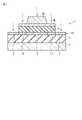
図1は、本実施形態に係る半導体装置1の一例を示す断面図である。
半導体装置1は、基材10と、第1絶縁層11と、第2絶縁層12と、第3絶縁層13と、バッファ層BLと、トランジスタTRと、を備えている。図1では、半導体装置1に含まれる1つのトランジスタTRを示している。トランジスタTRは、酸化物半導体層SCと、ゲート電極GEと、を備えている。<<
FIG. 1 is a cross-sectional view showing an example of a
The
第1絶縁層11は、基材10の上に配置されている。酸化物半導体層SCは、第1絶縁層11の上に配置されている。第2絶縁層12は、酸化物半導体層SCの上に配置されている。バッファ層BLは、第2絶縁層12の上に配置されている。ゲート電極GEは、バッファ層BLの上に配置されている。第3絶縁層13は、第2絶縁層12の上に配置され、ゲート電極GE及びバッファ層BLを覆っている。 The first
基材10は、ガラス、樹脂フィルム等の絶縁性の材料によって形成されている。
第1絶縁層11及び第2絶縁層12は、単層体であってもよいし、多層体であってもよい。一例では、第1絶縁層11及び第2絶縁層12は、シリコン酸化物層である。また、第1絶縁層11及び第2絶縁層12が多層体である場合、第1絶縁層11及び第2絶縁層12は、酸化物半導体層SCに接するシリコン酸化物層を含んでいる。The
The first
バッファ層BLは、例えば酸化物半導体層SCへのイオン注入を緩和する機能(イオン注入阻止能)、あるいは、酸化物半導体層SCへの水素拡散を緩和する機能(水素拡散阻止能)を有する層である。このようなバッファ層BLは、例えば、シリコン酸化物層、シリコン窒化物層、IGZO等の酸化物半導体層、チタン等の金属層のいずれかである。 The buffer layer BL is a layer having, for example, a function of mitigating ion implantation into the oxide semiconductor layer SC (ion implantation blocking power) or a function of mitigating hydrogen diffusion into the oxide semiconductor layer SC (hydrogen diffusion blocking power). is. Such a buffer layer BL is, for example, any one of a silicon oxide layer, a silicon nitride layer, an oxide semiconductor layer such as IGZO, and a metal layer such as titanium.
ゲート電極GEは、例えば、アルミニウム(Al)、チタン(Ti)、モリブデン(Mo)、タングステン(W)、銀(Ag)、Cu(銅)、Cr(クロム)などの金属材料や、これらの金属材料を組み合わせた合金などによって形成されている。ゲート電極GEの第1側面SS1は、傾斜面であることが望ましい。第1側面SS1とゲート電極GEに接するバッファ層BLの上面(あるいはゲート電極GEの下面)とのなす角度θは、鋭角である。 The gate electrode GE is made of, for example, metal materials such as aluminum (Al), titanium (Ti), molybdenum (Mo), tungsten (W), silver (Ag), Cu (copper), and Cr (chromium). It is made of an alloy or the like that combines materials. The first side surface SS1 of the gate electrode GE is preferably an inclined surface. The angle θ between the first side surface SS1 and the upper surface of the buffer layer BL (or the lower surface of the gate electrode GE) in contact with the gate electrode GE is an acute angle.
ゲート電極GEを挟んだ両側において、第1側面SS1は、バッファ層BLの第2側面SS2よりも内側に位置している。第1側面SS1から第2側面SS2までのバッファ層BLの幅Wは、ゲート電極GEを挟んだ両側でほぼ同等であり、0.5μm以上であることが望ましい。 On both sides of the gate electrode GE, the first side surface SS1 is located inside the second side surface SS2 of the buffer layer BL. The width W of the buffer layer BL from the first side surface SS1 to the second side surface SS2 is substantially the same on both sides of the gate electrode GE, and is preferably 0.5 μm or more.
第3絶縁層13は、例えば、シリコン窒化物層である。第3絶縁層13は、第1側面SS1と第2側面SS2との間でバッファ層BLに接し、また、第2側面SS2の外側で第2絶縁層12に接している。ゲート電極GEの第1側面SS1が傾斜面であるため、第3絶縁層13のクラックが抑制される。 The third insulating
酸化物半導体層SCは、チャネル領域Cと、ソース領域Sと、ドレイン領域Dと、低抵抗領域LSと、低抵抗領域LDと、を有している。チャネル領域Cは、ゲート電極GEの直下に位置している。ソース領域S及びドレイン領域Dは、第2絶縁層12及び第3絶縁層13が接する領域の直下に位置している。低抵抗領域LSは、チャネル領域Cとソース領域Sとの間に位置している。低抵抗領域LDは、チャネル領域Cとドレイン領域Dとの間に位置している。
また、低抵抗領域LS及び低抵抗領域LDは、バッファ層BL及び第3絶縁層13が接する領域の直下、あるいは、第1側面SS1と第2側面SS2との間の領域の直下に位置している。つまり、バッファ層BLは、チャネル領域C、低抵抗領域LS、及び、低抵抗領域LDに重畳し、ソース領域S及びドレイン領域Dには重畳していない。The oxide semiconductor layer SC has a channel region C, a source region S, a drain region D, a low resistance region LS, and a low resistance region LD. The channel region C is positioned directly below the gate electrode GE. The source region S and the drain region D are positioned directly below the region where the second insulating
In addition, the low resistance region LS and the low resistance region LD are located directly under the region where the buffer layer BL and the third insulating
低抵抗領域LS及び低抵抗領域LDは、チャネル領域Cと比較して、不純物濃度が高く、低抵抗である。ソース領域S及びドレイン領域Dは、低抵抗領域LS及びLDと比較して、不純物濃度が高く、低抵抗である。本明細書における不純物濃度とは、単位体積当たりの不純物数として表すことができる。なお、酸化物半導体について、不純物濃度が高いということは、単位体積当たりの酸素欠損数が多い、あるいは、単位体積当たりの欠陥数が多いことを意味するものである。 Compared to the channel region C, the low resistance region LS and the low resistance region LD have a higher impurity concentration and a lower resistance. The source region S and the drain region D have a higher impurity concentration and a lower resistance than the low resistance regions LS and LD. The impurity concentration in this specification can be expressed as the number of impurities per unit volume. Note that a high impurity concentration in an oxide semiconductor means that the number of oxygen vacancies per unit volume is large, or the number of defects per unit volume is large.
次に、上記の半導体装置1の製造方法について、図2及び図3を参照しながら説明する。 Next, a method for manufacturing the
まず、図2に示すように、基材10の上に、第1絶縁層11、酸化物半導体層SC、第2絶縁層12、バッファ層BL、及び、金属層Mを順次形成する。一例では、第1絶縁層11、第2絶縁層12、及び、バッファ層BLは、いずれもシリコン酸化物を堆積することによって形成される。その後、金属層Mの上に、所定の形状にパターニングしたレジストRを形成する。 First, as shown in FIG. 2, the first insulating
続いて、レジストRをマスクとして、バッファ層BL及び金属層Mをエッチング(ドライエッチング)し、第2絶縁層12の上面12Tを露出する。 Subsequently, using the resist R as a mask, the buffer layer BL and the metal layer M are etched (dry etched) to expose the
続いて、レジストRの体積を縮小し、金属層Mの側面SSに沿った上面MTを露出する。レジストRの体積を縮小する手法としては、例えば、アッシング処理が適用可能である。レジストRのアッシング処理を行うことにより、レジストRの体積は等方的に縮小する。このため、レジストRから露出した上面MTの面積あるいは上面MTの幅は、レジストRを挟んだ両側でほぼ同等である。レジストRから露出した上面MTの幅は、後に形成する低抵抗領域LS及びLDの幅と同等であり、例えば0.5μm以上である。 Subsequently, the volume of the resist R is reduced to expose the upper surface MT of the metal layer M along the side surfaces SS. As a technique for reducing the volume of the resist R, for example, an ashing process can be applied. By performing the ashing process of the resist R, the volume of the resist R is isotropically reduced. Therefore, the area of the upper surface MT exposed from the resist R or the width of the upper surface MT is substantially the same on both sides of the resist R. FIG. The width of the upper surface MT exposed from the resist R is equal to the width of the low resistance regions LS and LD to be formed later, and is, for example, 0.5 μm or more.
続いて、レジストRをマスクとして、金属層Mをエッチング(ドライエッチング)する。これにより、傾斜した第1側面SS1を有するゲート電極GEを形成するとともに、バッファ層BLの第2側面SS2に沿った上面BLTを露出する。レジストR及びゲート電極GEから露出した上面BLTの面積あるいは上面BLTの幅は、ゲート電極GEを挟んだ両側でほぼ同等である。 Subsequently, using the resist R as a mask, the metal layer M is etched (dry etched). As a result, the gate electrode GE having the inclined first side surface SS1 is formed, and the upper surface BLT along the second side surface SS2 of the buffer layer BL is exposed. The area of the upper surface BLT exposed from the resist R and the gate electrode GE or the width of the upper surface BLT is substantially the same on both sides of the gate electrode GE.
続いて、図3に示すように、ゲート電極GEをマスクとして、酸化物半導体層SCにイオン注入を行う。一例では、イオン注入により、不純物としてホウ素(B)を酸化物半導体層SCにドープする。なお、ホウ素の代わりに、リン(P)などの他の不純物を酸化物半導体層SCにドープしてもよい。この酸化物半導体層SCへのイオン注入は、レジストRを除去することなく行ってもよいし、レジストRを除去した後に行ってもよい。 Subsequently, as shown in FIG. 3, ions are implanted into the oxide semiconductor layer SC using the gate electrode GE as a mask. In one example, the oxide semiconductor layer SC is doped with boron (B) as an impurity by ion implantation. Instead of boron, other impurities such as phosphorus (P) may be doped into the oxide semiconductor layer SC. The ion implantation into the oxide semiconductor layer SC may be performed without removing the resist R, or may be performed after the resist R is removed.
これにより、酸化物半導体層SCには、ほとんど不純物がドープされないチャネル領域Cと、不純物がドープされたソース領域S及びドレイン領域Dと、チャネル領域Cとソース領域Sとの間に低抵抗領域LSと、チャネル領域Cとドレイン領域Dとの間に低抵抗領域LDとがそれぞれ形成される。上記の通り、バッファ層BLがイオン注入阻止能を有しているため、バッファ層BLの直下に位置する低抵抗領域LS及び低抵抗領域LDの不純物濃度は、バッファ層BLで覆われていないソース領域S及びドレイン領域Dの不純物濃度より低い。 Accordingly, the oxide semiconductor layer SC includes a channel region C that is hardly doped with impurities, a source region S and a drain region D that are doped with impurities, and a low-resistance region LS between the channel region C and the source region S. and a low resistance region LD are formed between the channel region C and the drain region D, respectively. As described above, since the buffer layer BL has an ion-implantation stopping power, the impurity concentration of the low-resistance region LS and the low-resistance region LD located directly under the buffer layer BL is equal to that of the source not covered with the buffer layer BL. It is lower than the impurity concentration of the region S and the drain region D.
その後、第3絶縁層13を形成することにより、図1に示した半導体装置1が製造される。 After that, the
以上説明したように、酸化物半導体層SCがチャネル領域Cに隣接した低抵抗領域LS及びLDを有しているため、酸化物半導体層SCに高電圧が印加された際の劣化を抑制することができる。したがって、不所望なしきい値電圧のシフトが抑制され、信頼性の低下が抑制される。 As described above, since the oxide semiconductor layer SC has the low-resistance regions LS and LD adjacent to the channel region C, deterioration when a high voltage is applied to the oxide semiconductor layer SC can be suppressed. can be done. Therefore, undesired threshold voltage shift is suppressed, and deterioration of reliability is suppressed.
また、このような低抵抗領域LS及びLDは、1回のイオン注入工程により、ソース領域S及びドレイン領域Dと同時に形成される。さらに、互いに側面の位置が異なるバッファ層BL及びゲート電極GEは、同一のレジストRを用いて形成される。したがって、半導体装置1の製造工程が簡素化される。 Also, the low-resistance regions LS and LD are formed at the same time as the source region S and the drain region D by one ion implantation process. Furthermore, the same resist R is used to form the buffer layer BL and the gate electrode GE, which have different side positions. Therefore, the manufacturing process of the
次に、半導体装置1の他の製造方法について、図4を参照しながら説明する。 Next, another manufacturing method of the
まず、基材10の上に、第1絶縁層11、酸化物半導体層SC、第2絶縁層12、バッファ層BL、及び、金属層Mを順次形成する。その後、金属層Mの上に、所定の形状にパターニングした第1レジストR1を形成する。 First, the first insulating
続いて、第1レジストR1をマスクとして、金属層Mをエッチング(ドライエッチング)する。これにより、ゲート電極GEを形成するとともに、バッファ層BLの上面BLTを露出する。その後、第1レジストR1を除去する。 Subsequently, using the first resist R1 as a mask, the metal layer M is etched (dry etched). As a result, the gate electrode GE is formed and the upper surface BLT of the buffer layer BL is exposed. After that, the first resist R1 is removed.
続いて、ゲート電極GEを覆うとともに、ゲート電極GEの両側のバッファ層BLの一部を覆う第2レジストR2を形成する。第2レジストR2が覆うバッファ層BLの幅は、後に形成する低抵抗領域LS及びLDの幅と同等であり、例えば0.5μm以上である。 Subsequently, a second resist R2 is formed to cover the gate electrode GE and part of the buffer layer BL on both sides of the gate electrode GE. The width of the buffer layer BL covered with the second resist R2 is equal to the width of the low-resistance regions LS and LD to be formed later, and is, for example, 0.5 μm or more.
続いて、第2レジストR2をマスクとして、バッファ層BLをエッチング(ドライエッチング)する。これにより、第2絶縁層12の上面12Tを露出する。その後、第2レジストR2を除去する。 Subsequently, using the second resist R2 as a mask, the buffer layer BL is etched (dry etched). Thereby, the
続いて、図3に示すように、ゲート電極GEをマスクとして、酸化物半導体層SCにイオン注入を行う。
その後、第3絶縁層13を形成することにより、図1に示した半導体装置1が製造される。Subsequently, as shown in FIG. 3, ions are implanted into the oxide semiconductor layer SC using the gate electrode GE as a mask.
After that, the
このような他の製造方法においても、低抵抗領域LS及びLDは、1回のイオン注入工程により、ソース領域S及びドレイン領域Dと同時に形成される。したがって、半導体装置1の製造工程が簡素化される。 Also in this other manufacturing method, the low-resistance regions LS and LD are formed at the same time as the source region S and the drain region D by one ion implantation process. Therefore, the manufacturing process of the
《構成2》
図5は、本実施形態に係る半導体装置1の他の例を示す断面図である。
図5に示す例は、図1に示した例と比較して、酸化物半導体層SCのうち、ソース領域S及びドレイン領域Dが第2絶縁層12から露出している点で相違している。ここでは、図1に示した例と同一構成については、説明を省略する場合がある。<<
FIG. 5 is a cross-sectional view showing another example of the
The example shown in FIG. 5 is different from the example shown in FIG. 1 in that the source region S and the drain region D of the oxide semiconductor layer SC are exposed from the second insulating
ゲート電極GEを挟んだ両側において、ゲート電極GEの第1側面SS1は、バッファ層BLの第2側面SS2及び第2絶縁層12の第3側面SS3よりも内側に位置している。第2側面SS2は、第3側面SS3の直上に位置している。第1側面SS1から第2側面SS2までの幅W(あるいは第1側面SS1から第3側面SS3までの幅)は、ゲート電極GEを挟んだ両側でほぼ同等であり、0.5μm以上であることが望ましい。 On both sides of the gate electrode GE, the first side surface SS1 of the gate electrode GE is positioned inside the second side surface SS2 of the buffer layer BL and the third side surface SS3 of the second insulating
第3絶縁層13は、ゲート電極GE、バッファ層BL、第2絶縁層12、及び、酸化物半導体層SCを覆っている。図示した例では、第3絶縁層13は、ゲート電極GEを覆うとともに、第1側面SS1と第2側面SS2との間でバッファ層BLに接し、第2側面SS2及び第3側面SS3に接し、第3側面SS3の外側で酸化物半導体層SCに接している。 The third insulating
酸化物半導体層SCにおいて、チャネル領域Cは、ゲート電極GEの直下に位置している。ソース領域S及びドレイン領域Dは、第3絶縁層13に接している。低抵抗領域LS及び低抵抗領域LDは、バッファ層BL及び第3絶縁層13が接する領域の直下、あるいは、第1側面SS1と第2側面SS2との間の領域の直下、あるいは、第1側面SS1と第3側面SS3との間の領域の直下に位置している。つまり、第2絶縁層12及びバッファ層BLの積層体は、チャネル領域C、低抵抗領域LS、及び、低抵抗領域LDに重畳し、ソース領域S及びドレイン領域Dには重畳していない。 In the oxide semiconductor layer SC, the channel region C is located directly below the gate electrode GE. The source region S and drain region D are in contact with the third insulating
次に、上記の半導体装置1の製造方法について、図6及び図7を参照しながら説明する。 Next, a method for manufacturing the
まず、図6に示すように、基材10の上に、第1絶縁層11、酸化物半導体層SC、第2絶縁層12、バッファ層BL、及び、金属層Mを順次形成する。一例では、第1絶縁層11、第2絶縁層12、及び、バッファ層BLは、いずれもシリコン酸化物を堆積することによって形成される。その後、金属層Mの上に、所定の形状にパターニングしたレジストRを形成する。 First, as shown in FIG. 6, the first insulating
続いて、レジストRをマスクとして、第2絶縁層12、バッファ層BL、及び、金属層Mをエッチング(ドライエッチング)し、酸化物半導体層SCの上面SCTを露出する。 Subsequently, using the resist R as a mask, the second insulating
続いて、レジストRの体積を縮小し、金属層Mの側面SSに沿った上面MTを露出する。レジストRの体積を縮小する手法として、例えば、アッシング処理が適用可能である。 Subsequently, the volume of the resist R is reduced to expose the upper surface MT of the metal layer M along the side surfaces SS. As a technique for reducing the volume of the resist R, for example, an ashing process can be applied.
続いて、レジストRをマスクとして、金属層Mをエッチング(ドライエッチング)する。これにより、傾斜した第1側面SS1を有するゲート電極GEを形成するとともに、バッファ層BLの第2側面SS2に沿った上面BLTを露出する。 Subsequently, using the resist R as a mask, the metal layer M is etched (dry etched). As a result, the gate electrode GE having the inclined first side surface SS1 is formed, and the upper surface BLT along the second side surface SS2 of the buffer layer BL is exposed.
続いて、図7に示すように、酸化物半導体層SCの還元処理を行う。一例では、還元処理は、水素プラズマ処理である。この水素プラズマ処理は、レジストRを除去することなく行ってもよいし、レジストRを除去した後に行ってもよい。 Subsequently, as shown in FIG. 7, the oxide semiconductor layer SC is subjected to reduction treatment. In one example, the reduction treatment is hydrogen plasma treatment. This hydrogen plasma treatment may be performed without removing the resist R, or may be performed after the resist R is removed.
これにより、酸化物半導体層SCのうち、露出した部分は、水素による還元作用によって低抵抗化され、ソース領域S及びドレイン領域Dとして形成される。また、酸化物半導体層SCのうち、第2絶縁層12及びバッファ層BLの積層体が重畳する部分は、この積層体を透過した水素、あるいは、ソース領域Sまたはドレイン領域Dから拡散した水素による還元作用によって低抵抗化され、低抵抗領域LS及び低抵抗領域LDとして形成される。但し、低抵抗領域LS及び低抵抗領域LDへの水素供給量は、ソース領域S及びドレイン領域Dへの水素供給量より少ない。このため、低抵抗領域LS及び低抵抗領域LDは、ソース領域S及びドレイン領域Dよりも高抵抗である。一方、酸化物半導体層SCのうち、ゲート電極GEの直下の部分は、ほとんど水素による還元作用を受けず、チャネル領域Cとして形成される。このため、チャネル領域Cは、低抵抗領域LS及び低抵抗領域LDよりも高抵抗である。 As a result, the exposed portions of the oxide semiconductor layer SC are reduced in resistance by the reduction action of hydrogen, and formed as the source region S and the drain region D. As shown in FIG. In addition, the portion of the oxide semiconductor layer SC where the stacked body of the second insulating
その後、第3絶縁層13を形成することにより、図5に示した半導体装置1が製造される。 After that, by forming the third insulating
なお、上記の例では、還元処理が水素プラズマ処理である場合について説明したが、還元処理はこれに限らない。例えば、第3絶縁層13を形成するに際して、シリコン窒化物を堆積して第3絶縁層13を形成する。これにより、酸化物半導体層SCのうち、第3絶縁層13に接する部分は、第3絶縁層13を形成する過程で水素による還元作用を受けて低抵抗され、ソース領域S及びドレイン領域Dとして形成される。その後、アニールを行うことで、ソース領域S及びドレイン領域Dにそれぞれ含まれる水素が拡散し、酸化物半導体層SCのうち、ソース領域Sに隣接する部分が低抵抗されて低抵抗領域LSとして形成され、また、ドレイン領域Dに隣接する部分が低抵抗化されて低抵抗領域LDとして形成される。 In the above example, the case where the reduction treatment is hydrogen plasma treatment has been described, but the reduction treatment is not limited to this. For example, when forming the third insulating
以上説明したように、酸化物半導体層SCがチャネル領域Cに隣接した低抵抗領域LS及びLDを有しているため、上記の構成1と同様の効果が得られる。 As described above, since the oxide semiconductor layer SC has the low-resistance regions LS and LD adjacent to the channel region C, the same effects as those of the
また、このような低抵抗領域LS及びLDは、酸化物半導体層SCの還元処理により、ソース領域S及びドレイン領域Dとほぼ同時に形成される。さらに、互いに側面の位置が異なるバッファ層BL及びゲート電極GEは、同一のレジストRを用いて形成される。したがって、半導体装置1の製造工程が簡素化される。 Further, such low-resistance regions LS and LD are formed substantially at the same time as the source region S and the drain region D by reduction treatment of the oxide semiconductor layer SC. Furthermore, the same resist R is used to form the buffer layer BL and the gate electrode GE, which have different side positions. Therefore, the manufacturing process of the
次に、半導体装置1の他の製造方法について、図8を参照しながら説明する。 Next, another method for manufacturing the
まず、基材10の上に、第1絶縁層11、酸化物半導体層SC、第2絶縁層12、バッファ層BL、及び、金属層Mを順次形成する。その後、金属層Mの上に、所定の形状にパターニングした第1レジストR1を形成する。 First, the first insulating
続いて、第1レジストR1をマスクとして、金属層Mをエッチング(ドライエッチング)する。これにより、ゲート電極GEを形成するとともに、バッファ層BLの上面BLTを露出する。その後、第1レジストR1を除去する。 Subsequently, using the first resist R1 as a mask, the metal layer M is etched (dry etched). As a result, the gate electrode GE is formed and the upper surface BLT of the buffer layer BL is exposed. After that, the first resist R1 is removed.
続いて、ゲート電極GEを覆うとともに、ゲート電極GEの両側のバッファ層BLの一部を覆う第2レジストR2を形成する。 Subsequently, a second resist R2 is formed to cover the gate electrode GE and part of the buffer layer BL on both sides of the gate electrode GE.
続いて、第2レジストR2をマスクとして、第2絶縁層12及びバッファ層BLをエッチング(ドライエッチング)する。これにより、酸化物半導体層SCの上面SCTを露出する。その後、第2レジストR2を除去する。 Subsequently, using the second resist R2 as a mask, the second insulating
続いて、酸化物半導体層SCの還元処理を行う。
その後、第3絶縁層13を形成することにより、図5に示した半導体装置1が製造される。この例においても、酸化物半導体層SCの還元処理は、上記のプラズマ処理でもよいし、シリコン窒化物層の堆積及び水素拡散処理の組合せであってもよい。Subsequently, reduction treatment of the oxide semiconductor layer SC is performed.
After that, by forming the third insulating
このような他の製造方法においても、低抵抗領域LS及びLDは、酸化物半導体層SCの還元処理により、ソース領域S及びドレイン領域Dとほぼ同時に形成される。したがって、半導体装置1の製造工程が簡素化される。 Also in such another manufacturing method, the low-resistance regions LS and LD are formed substantially at the same time as the source region S and the drain region D by the reduction treatment of the oxide semiconductor layer SC. Therefore, the manufacturing process of the
次に、図1に示した断面図における点線で囲んだ部分P1及びP2を想定して、部分P1及びP2における不純物濃度をシミュレーションにより算出した。このシミュレーションでは、不純物濃度として、ホウ素の濃度を算出した。 Next, assuming the portions P1 and P2 enclosed by the dotted lines in the cross-sectional view shown in FIG. 1, the impurity concentrations in the portions P1 and P2 were calculated by simulation. In this simulation, the concentration of boron was calculated as the impurity concentration.
部分P1は、第1絶縁層11、酸化物半導体層SC、及び、第2絶縁層12を積層した領域であり、バッファ層BLが存在しない。つまり、バッファ層BLの膜厚は0nmである。
部分P2は、第1絶縁層11、酸化物半導体層SC、第2絶縁層12、及び、バッファ層BLを積層した領域である。The portion P1 is a region in which the first insulating
The portion P2 is a region in which the first insulating
図9は、シミュレーション結果を示す図である。ここでは、イオン注入の際の加速エネルギーを30keVとし、イオンのドーズ量を1*1015ions/cm2とする。FIG. 9 is a diagram showing simulation results. Here, the acceleration energy for ion implantation is 30 keV, and the dose of ions is 1*1015 ions/cm2 .
図の横軸は、深さ方向の距離(nm)である。深さ方向の位置に関して、グラフの左方向が部分P1及びP2の上方向に相当し、グラフの右方向が部分P1及びP2の下方向に相当する。グラフの上部には、バッファ層の範囲を「BL」と示し、第2絶縁層の範囲を「12」と示し、酸化物半導体層の範囲を「SC」と示し、第1絶縁層の範囲を「11」と示している。
第2絶縁層12の膜厚は100nmであり、酸化物半導体層SCの膜厚は15nmである。バッファ層BLは、シリコン酸化物層である。The horizontal axis of the figure is the distance (nm) in the depth direction. Regarding positions in the depth direction, the left direction of the graph corresponds to the upward direction of the portions P1 and P2, and the right direction of the graph corresponds to the downward direction of the portions P1 and P2. At the top of the graph, the range of the buffer layer is indicated as "BL", the range of the second insulating layer is indicated as "12", the range of the oxide semiconductor layer is indicated as "SC", and the range of the first insulating layer is indicated as "SC". "11" is indicated.
The thickness of the second insulating
図の縦軸は、不純物であるホウ素の濃度(atoms/cm3)である。The vertical axis of the figure is the concentration of boron as an impurity (atoms/cm3 ).
バッファ層BLの膜厚が0nmの場合のシミュレーション結果T0は、バッファ層BLが存在しない部分P1のシミュレーション結果に相当する。バッファ層BLの膜厚が25nmの場合のシミュレーション結果T25、バッファ層BLの膜厚が50nmの場合のシミュレーション結果T50、バッファ層BLの膜厚が75nmの場合のシミュレーション結果T75、及び、バッファ層BLの膜厚が100nmの場合のシミュレーション結果T100は、バッファ層BLが存在する部分P2のシミュレーション結果に相当する。 The simulation result T0 when the film thickness of the buffer layer BL is 0 nm corresponds to the simulation result of the portion P1 where the buffer layer BL does not exist. Simulation result T25 when the thickness of the buffer layer BL is 25 nm, simulation result T50 when the thickness of the buffer layer BL is 50 nm, simulation result T75 when the thickness of the buffer layer BL is 75 nm, and the buffer layer BL is 100 nm, the simulation result T100 corresponds to the simulation result of the portion P2 where the buffer layer BL exists.
図9に示すシミュレーション結果によれば、部分P1における酸化物半導体層SCの不純物濃度に対して、バッファ層BLの膜厚が100nmであれば、部分P2における酸化物半導体層SCの不純物濃度を1桁以上小さくできることが確認された。このことは、部分P2における酸化物半導体層SCが低抵抗領域LDまたはLSとして機能することを意味するものである。 According to the simulation results shown in FIG. 9, with respect to the impurity concentration of the oxide semiconductor layer SC in the portion P1, if the thickness of the buffer layer BL is 100 nm, the impurity concentration of the oxide semiconductor layer SC in the portion P2 is 1. It was confirmed that it can be made smaller by an order of magnitude or more. This means that the oxide semiconductor layer SC in the portion P2 functions as the low resistance region LD or LS.
ここでは、バッファ層BLとして、シリコン酸化物層を想定しているが、シリコン酸化物よりも高密度の材料でバッファ層BLを形成した場合には、上記のシミュレーションよりもさらに薄い膜厚のバッファ層BLであっても、十分なイオン注入阻止能、あるいは、水素拡散阻止能を発揮することができる。 Here, a silicon oxide layer is assumed as the buffer layer BL, but if the buffer layer BL is formed of a material with a higher density than silicon oxide, the buffer layer may have a thinner film thickness than the above simulation. Even the layer BL can exhibit sufficient ion-implantation stopping power or hydrogen diffusion stopping power.
以上説明したように、本実施形態によれば、信頼性の低下を抑制する半導体装置の製造工程が簡素化される製造方法を提供することができる。 As described above, according to this embodiment, it is possible to provide a manufacturing method that simplifies the manufacturing process of a semiconductor device that suppresses deterioration in reliability.
以上、本発明の実施形態として説明した半導体装置の製造方法を基にして、当業者が適宜設計変更して実施し得る全ての半導体装置の製造方法も、本発明の要旨を包含する限り、本発明の範囲に属する。 Based on the semiconductor device manufacturing methods described as the embodiments of the present invention, all semiconductor device manufacturing methods that can be implemented by a person skilled in the art by appropriately modifying the design are included in the present invention as long as they include the gist of the present invention. It belongs to the scope of the invention.
本発明の思想の範疇において、当業者であれば、各種の変形例に想到し得るものであり、それら変形例についても本発明の範囲に属するものと解される。例えば、上述の実施形態に対して、当業者が適宜、構成要素の追加、削除、もしくは設計変更を行ったもの、または、工程の追加、省略もしくは条件変更を行ったものも、本発明の要旨を備えている限り、本発明の範囲に含まれる。 Within the scope of the idea of the present invention, those skilled in the art can conceive of various modifications, and these modifications are also understood to belong to the scope of the present invention. For example, additions, deletions, or design changes of components, or additions, omissions, or changes in the conditions of the above-described embodiments by those skilled in the art are also subject to the gist of the present invention. is included in the scope of the present invention as long as it has
また、上述の実施形態において述べた態様によりもたらされる他の作用効果について、本明細書の記載から明らかなもの、または当業者において適宜想到し得るものについては、当然に本発明によりもたらされるものと解される。 In addition, other actions and effects brought about by the aspects described in the above-described embodiments, which are obvious from the description of the present specification or which can be appropriately conceived by those skilled in the art, are naturally brought about by the present invention. solved.
1…半導体装置 TR…トランジスタ 10…基材
11…第1絶縁層 12…第2絶縁層 13…第3絶縁層 GE…ゲート電極
SC…酸化物半導体層 C…チャネル領域 LS、LD…低抵抗領域 S…ソース領域 D…ドレイン領域
BL…バッファ層DESCRIPTION OF
Claims (10)
Translated fromJapanese前記金属層の上に、パターニングしたレジストを形成し、
前記レジストをマスクとして、前記バッファ層及び前記金属層をエッチングし、前記第2絶縁層の上面を露出し、
前記レジストの体積を縮小し、前記金属層の側面に沿った上面を露出し、
前記レジストをマスクとして、前記金属層をエッチングし、第1側面を有するゲート電極を形成するとともに、前記バッファ層の第2側面に沿った上面を露出し、
前記ゲート電極をマスクとして、前記酸化物半導体層にイオン注入を行う、半導体装置の製造方法。sequentially forming a first insulating layer, an oxide semiconductor layer, a second insulating layer, a buffer layer, and a metal layer on a substrate;
forming a patterned resist on the metal layer;
etching the buffer layer and the metal layer using the resist as a mask to expose an upper surface of the second insulating layer;
reducing the volume of the resist to expose the upper surface along the sides of the metal layer;
etching the metal layer using the resist as a mask to form a gate electrode having a first side surface and exposing an upper surface along the second side surface of the buffer layer;
A method of manufacturing a semiconductor device, wherein ions are implanted into the oxide semiconductor layer using the gate electrode as a mask.
前記金属層の上に、パターニングしたレジストを形成し、
前記レジストをマスクとして、前記第2絶縁層、前記バッファ層、及び、前記金属層をエッチングし、前記酸化物半導体層の上面を露出し、
前記レジストの体積を縮小し、前記金属層の側面に沿った上面を露出し、
前記レジストをマスクとして、前記金属層をエッチングし、第1側面を有するゲート電極を形成するとともに、前記バッファ層の第2側面に沿った上面を露出し、
前記酸化物半導体層の還元処理を行う、半導体装置の製造方法。sequentially forming a first insulating layer, an oxide semiconductor layer, a second insulating layer, a buffer layer, and a metal layer on a substrate;
forming a patterned resist on the metal layer;
using the resist as a mask, etching the second insulating layer, the buffer layer, and the metal layer to expose an upper surface of the oxide semiconductor layer;
reducing the volume of the resist to expose the upper surface along the sides of the metal layer;
etching the metal layer using the resist as a mask to form a gate electrode having a first side surface and exposing an upper surface along the second side surface of the buffer layer;
A method for manufacturing a semiconductor device, wherein the oxide semiconductor layer is subjected to reduction treatment.
前記金属層の上に、パターニングした第1レジストを形成し、
前記第1レジストをマスクとして、前記金属層をエッチングし、ゲート電極を形成するとともに、前記バッファ層の上面を露出し、
前記第1レジストを除去した後に、前記ゲート電極、及び、前記ゲート電極の両側の前記バッファ層の一部を覆う第2レジストを形成し、
前記第2レジストをマスクとして、前記バッファ層をエッチングし、前記第2絶縁層の上面を露出し、
前記第2レジストを除去した後に、前記ゲート電極をマスクとして、前記酸化物半導体層にイオン注入を行う、半導体装置の製造方法。sequentially forming a first insulating layer, an oxide semiconductor layer, a second insulating layer, a buffer layer, and a metal layer on a substrate;
forming a patterned first resist on the metal layer;
using the first resist as a mask, etching the metal layer to form a gate electrode and exposing the upper surface of the buffer layer;
forming a second resist covering the gate electrode and a portion of the buffer layer on both sides of the gate electrode after removing the first resist;
etching the buffer layer using the second resist as a mask to expose the upper surface of the second insulating layer;
The method of manufacturing a semiconductor device, wherein, after removing the second resist, ions are implanted into the oxide semiconductor layer using the gate electrode as a mask.
前記金属層の上に、パターニングした第1レジストを形成し、
前記第1レジストをマスクとして、前記金属層をエッチングし、ゲート電極を形成するとともに、前記バッファ層の上面を露出し、
前記第1レジストを除去した後に、前記ゲート電極、及び、前記ゲート電極の両側の前記バッファ層の一部を覆う第2レジストを形成し、
前記第2レジストをマスクとして、前記前記第2絶縁層及び前記バッファ層をエッチングし、前記酸化物半導体層の上面を露出し、
前記第2レジストを除去した後に、前記酸化物半導体層の還元処理を行う、半導体装置の製造方法。sequentially forming a first insulating layer, an oxide semiconductor layer, a second insulating layer, a buffer layer, and a metal layer on a substrate;
forming a patterned first resist on the metal layer;
using the first resist as a mask, etching the metal layer to form a gate electrode and exposing the upper surface of the buffer layer;
forming a second resist covering the gate electrode and a portion of the buffer layer on both sides of the gate electrode after removing the first resist;
etching the second insulating layer and the buffer layer using the second resist as a mask to expose an upper surface of the oxide semiconductor layer;
The method of manufacturing a semiconductor device, wherein the oxide semiconductor layer is subjected to reduction treatment after removing the second resist.
Priority Applications (3)
| Application Number | Priority Date | Filing Date | Title |
|---|---|---|---|
| JP2021080436AJP2022174557A (en) | 2021-05-11 | 2021-05-11 | Method for manufacturing semiconductor device |
| US17/660,729US12294024B2 (en) | 2021-05-11 | 2022-04-26 | Method of manufacturing semiconductor device |
| US19/171,436US20250234655A1 (en) | 2021-05-11 | 2025-04-07 | Method of manufacturing semiconductor device |
Applications Claiming Priority (1)
| Application Number | Priority Date | Filing Date | Title |
|---|---|---|---|
| JP2021080436AJP2022174557A (en) | 2021-05-11 | 2021-05-11 | Method for manufacturing semiconductor device |
Publications (1)
| Publication Number | Publication Date |
|---|---|
| JP2022174557Atrue JP2022174557A (en) | 2022-11-24 |
Family
ID=83998086
Family Applications (1)
| Application Number | Title | Priority Date | Filing Date |
|---|---|---|---|
| JP2021080436APendingJP2022174557A (en) | 2021-05-11 | 2021-05-11 | Method for manufacturing semiconductor device |
Country Status (2)
| Country | Link |
|---|---|
| US (2) | US12294024B2 (en) |
| JP (1) | JP2022174557A (en) |
Families Citing this family (1)
| Publication number | Priority date | Publication date | Assignee | Title |
|---|---|---|---|---|
| US11322442B2 (en) | 2018-01-05 | 2022-05-03 | Semiconductor Energy Laboratory Co., Ltd. | Semiconductor device including transistor with oxide semiconductor and method for manufacturing the semiconductor device |
Family Cites Families (28)
| Publication number | Priority date | Publication date | Assignee | Title |
|---|---|---|---|---|
| JP4021194B2 (en)* | 2001-12-28 | 2007-12-12 | シャープ株式会社 | Method for manufacturing thin film transistor device |
| US6846707B2 (en)* | 2003-05-15 | 2005-01-25 | Au Optronics Corp. | Method for forming a self-aligned LTPS TFT |
| US7064021B2 (en)* | 2003-07-02 | 2006-06-20 | Au Optronics Corp. | Method for fomring a self-aligned LTPS TFT |
| KR20130111872A (en)* | 2012-04-02 | 2013-10-11 | 삼성디스플레이 주식회사 | Thin film transistor, thin film transistor array panel including the same and manufacturing method thereof |
| KR20140032155A (en)* | 2012-09-06 | 2014-03-14 | 삼성디스플레이 주식회사 | Thin-film transistor substrate and method of manufacturing the same |
| KR102131195B1 (en)* | 2013-07-16 | 2020-07-08 | 삼성디스플레이 주식회사 | Display substrate having a thin film transistor and method of manufacturing the same |
| CN103745954B (en)* | 2014-01-03 | 2017-01-25 | 京东方科技集团股份有限公司 | Display device, array substrate and manufacturing method of array substrate |
| CN104253159B (en)* | 2014-08-19 | 2017-06-13 | 京东方科技集团股份有限公司 | Thin film transistor (TFT) and preparation method, array base palte and preparation method and display device |
| CN104701254B (en)* | 2015-03-16 | 2017-10-03 | 深圳市华星光电技术有限公司 | A kind of preparation method of low-temperature polysilicon film transistor array base palte |
| CN104867959B (en)* | 2015-04-14 | 2017-09-26 | 深圳市华星光电技术有限公司 | The preparation method and its structure of dual gate oxide semiconductor TFT substrate |
| CN104900531A (en)* | 2015-06-08 | 2015-09-09 | 京东方科技集团股份有限公司 | Oxide thin-film transistor and array substrate, and manufacturing methods thereof, and display apparatus |
| CN105390451B (en)* | 2015-12-03 | 2018-03-30 | 深圳市华星光电技术有限公司 | The preparation method of low temperature polycrystalline silicon TFT substrate |
| JP6827270B2 (en) | 2016-03-28 | 2021-02-10 | 株式会社ジャパンディスプレイ | Manufacturing method of semiconductor device |
| CN105633016B (en)* | 2016-03-30 | 2019-04-02 | 深圳市华星光电技术有限公司 | The production method of TFT substrate and TFT substrate obtained |
| CN105655359A (en)* | 2016-03-31 | 2016-06-08 | 武汉华星光电技术有限公司 | Method for manufacturing TFT (thin-film transistor) substrates |
| US20190074383A1 (en)* | 2017-09-04 | 2019-03-07 | Shenzhen China Star Optoelectronics Semiconductor Display Technology Co., Ltd. | Thin film transistor structure and driving circuit of amoled |
| CN107799570A (en)* | 2017-10-09 | 2018-03-13 | 深圳市华星光电半导体显示技术有限公司 | Top-gated autoregistration metal-oxide semiconductor (MOS) TFT and preparation method thereof |
| CN107689345B (en)* | 2017-10-09 | 2020-04-28 | 深圳市华星光电半导体显示技术有限公司 | TFT substrate and manufacturing method thereof, and OLED panel and manufacturing method thereof |
| CN108511464B (en)* | 2018-04-20 | 2020-07-28 | 武汉华星光电技术有限公司 | Manufacturing method of CMOS L TPS TFT substrate |
| CN108878449B (en)* | 2018-06-28 | 2020-07-03 | 京东方科技集团股份有限公司 | Manufacturing method of array substrate, array substrate and display device |
| US20200127141A1 (en)* | 2018-10-23 | 2020-04-23 | HKC Corporation Limited | Method for manufacturing thin film transistor, thin film transistor, and display panel |
| JP2020129635A (en) | 2019-02-12 | 2020-08-27 | 株式会社ジャパンディスプレイ | Semiconductor device and method of manufacturing the same |
| CN110416313A (en)* | 2019-07-19 | 2019-11-05 | 深圳市华星光电半导体显示技术有限公司 | Thin film transistor substrate and manufacturing method thereof |
| CN111370428B (en)* | 2020-03-19 | 2023-02-28 | 合肥鑫晟光电科技有限公司 | Display substrate, manufacturing method thereof, and display device |
| US11757047B2 (en)* | 2020-05-29 | 2023-09-12 | Taiwan Semiconductor Manufacturing Company Limited | Semiconducting metal oxide transistors having a patterned gate and methods for forming the same |
| CN111725324B (en)* | 2020-06-11 | 2021-11-02 | 武汉华星光电半导体显示技术有限公司 | Thin film transistor, array substrate and manufacturing method thereof |
| JP2022090361A (en)* | 2020-12-07 | 2022-06-17 | 株式会社ジャパンディスプレイ | Semiconductor devices and their manufacturing methods |
| CN114937701B (en)* | 2022-04-14 | 2025-05-27 | 深圳市华星光电半导体显示技术有限公司 | Array substrate and manufacturing method thereof, and display panel |
- 2021
- 2021-05-11JPJP2021080436Apatent/JP2022174557A/enactivePending
- 2022
- 2022-04-26USUS17/660,729patent/US12294024B2/enactiveActive
- 2025
- 2025-04-07USUS19/171,436patent/US20250234655A1/enactivePending
Also Published As
| Publication number | Publication date |
|---|---|
| US20220367691A1 (en) | 2022-11-17 |
| US12294024B2 (en) | 2025-05-06 |
| US20250234655A1 (en) | 2025-07-17 |
Similar Documents
| Publication | Publication Date | Title |
|---|---|---|
| KR100387389B1 (en) | Semiconductor device and manufacturing method of the same | |
| JP5475260B2 (en) | Wiring structure, thin film transistor substrate, manufacturing method thereof, and display device | |
| TWI814636B (en) | Active device substrate | |
| WO2010001998A1 (en) | Wiring structure, thin film transistor substrate, method for manufacturing thin film transistor substrate, and display device | |
| US9214354B2 (en) | Manufacturing method for semiconductor device | |
| JP2022183298A5 (en) | ||
| US20250234655A1 (en) | Method of manufacturing semiconductor device | |
| CN104716101A (en) | Manufacturing method for semiconductor device | |
| EP3449498B1 (en) | Thin film transistor, display apparatus having the same, and fabricating method thereof | |
| KR102148957B1 (en) | Display substrate and method of manufacturing a display substrate | |
| CN109962106B (en) | MOSFET device and method of manufacturing the same | |
| US20240297250A1 (en) | Method of manufacturing semiconductor device and semiconductor device | |
| CN105810573A (en) | Manufacturing method of thin-film transistor | |
| CN1523675A (en) | Semiconductor device and manufacturing method thereof | |
| CN107179644B (en) | Display substrate, manufacturing method thereof and display device | |
| CN105633171A (en) | Thin film transistor and manufacturing method therefor, and display apparatus | |
| JP2024001641A (en) | Semiconductor device and manufacturing method thereof | |
| KR20040022373A (en) | Semiconductor device and method of manufacturing the same | |
| CN109860107B (en) | Array substrate and manufacturing method thereof | |
| CN114335011A (en) | Display panel and preparation method thereof | |
| CN106611794A (en) | Thin film transistor and making method thereof | |
| JP2023054475A (en) | Semiconductor device and its manufacturing method | |
| JP2016018938A (en) | Semiconductor device and manufacturing method thereof | |
| KR102803695B1 (en) | Semiconductor device | |
| US12166070B2 (en) | Semiconductor transistor structure and manufacturing method |