JP2022169671A - non-rectangular display - Google Patents
non-rectangular displayDownload PDFInfo
- Publication number
- JP2022169671A JP2022169671AJP2022131286AJP2022131286AJP2022169671AJP 2022169671 AJP2022169671 AJP 2022169671AJP 2022131286 AJP2022131286 AJP 2022131286AJP 2022131286 AJP2022131286 AJP 2022131286AJP 2022169671 AJP2022169671 AJP 2022169671A
- Authority
- JP
- Japan
- Prior art keywords
- display area
- pixel
- pixels
- driving circuit
- circuits
- Prior art date
- Legal status (The legal status is an assumption and is not a legal conclusion. Google has not performed a legal analysis and makes no representation as to the accuracy of the status listed.)
- Pending
Links
Images


Classifications
- G—PHYSICS
- G09—EDUCATION; CRYPTOGRAPHY; DISPLAY; ADVERTISING; SEALS
- G09G—ARRANGEMENTS OR CIRCUITS FOR CONTROL OF INDICATING DEVICES USING STATIC MEANS TO PRESENT VARIABLE INFORMATION
- G09G3/00—Control arrangements or circuits, of interest only in connection with visual indicators other than cathode-ray tubes
- G09G3/20—Control arrangements or circuits, of interest only in connection with visual indicators other than cathode-ray tubes for presentation of an assembly of a number of characters, e.g. a page, by composing the assembly by combination of individual elements arranged in a matrix no fixed position being assigned to or needed to be assigned to the individual characters or partial characters
- G09G3/22—Control arrangements or circuits, of interest only in connection with visual indicators other than cathode-ray tubes for presentation of an assembly of a number of characters, e.g. a page, by composing the assembly by combination of individual elements arranged in a matrix no fixed position being assigned to or needed to be assigned to the individual characters or partial characters using controlled light sources
- G09G3/30—Control arrangements or circuits, of interest only in connection with visual indicators other than cathode-ray tubes for presentation of an assembly of a number of characters, e.g. a page, by composing the assembly by combination of individual elements arranged in a matrix no fixed position being assigned to or needed to be assigned to the individual characters or partial characters using controlled light sources using electroluminescent panels
- G09G3/32—Control arrangements or circuits, of interest only in connection with visual indicators other than cathode-ray tubes for presentation of an assembly of a number of characters, e.g. a page, by composing the assembly by combination of individual elements arranged in a matrix no fixed position being assigned to or needed to be assigned to the individual characters or partial characters using controlled light sources using electroluminescent panels semiconductive, e.g. using light-emitting diodes [LED]
- G09G3/3208—Control arrangements or circuits, of interest only in connection with visual indicators other than cathode-ray tubes for presentation of an assembly of a number of characters, e.g. a page, by composing the assembly by combination of individual elements arranged in a matrix no fixed position being assigned to or needed to be assigned to the individual characters or partial characters using controlled light sources using electroluminescent panels semiconductive, e.g. using light-emitting diodes [LED] organic, e.g. using organic light-emitting diodes [OLED]
- G09G3/3225—Control arrangements or circuits, of interest only in connection with visual indicators other than cathode-ray tubes for presentation of an assembly of a number of characters, e.g. a page, by composing the assembly by combination of individual elements arranged in a matrix no fixed position being assigned to or needed to be assigned to the individual characters or partial characters using controlled light sources using electroluminescent panels semiconductive, e.g. using light-emitting diodes [LED] organic, e.g. using organic light-emitting diodes [OLED] using an active matrix
- G09G3/3258—Control arrangements or circuits, of interest only in connection with visual indicators other than cathode-ray tubes for presentation of an assembly of a number of characters, e.g. a page, by composing the assembly by combination of individual elements arranged in a matrix no fixed position being assigned to or needed to be assigned to the individual characters or partial characters using controlled light sources using electroluminescent panels semiconductive, e.g. using light-emitting diodes [LED] organic, e.g. using organic light-emitting diodes [OLED] using an active matrix with pixel circuitry controlling the voltage across the light-emitting element
- G—PHYSICS
- G09—EDUCATION; CRYPTOGRAPHY; DISPLAY; ADVERTISING; SEALS
- G09G—ARRANGEMENTS OR CIRCUITS FOR CONTROL OF INDICATING DEVICES USING STATIC MEANS TO PRESENT VARIABLE INFORMATION
- G09G3/00—Control arrangements or circuits, of interest only in connection with visual indicators other than cathode-ray tubes
- G09G3/20—Control arrangements or circuits, of interest only in connection with visual indicators other than cathode-ray tubes for presentation of an assembly of a number of characters, e.g. a page, by composing the assembly by combination of individual elements arranged in a matrix no fixed position being assigned to or needed to be assigned to the individual characters or partial characters
- G—PHYSICS
- G02—OPTICS
- G02F—OPTICAL DEVICES OR ARRANGEMENTS FOR THE CONTROL OF LIGHT BY MODIFICATION OF THE OPTICAL PROPERTIES OF THE MEDIA OF THE ELEMENTS INVOLVED THEREIN; NON-LINEAR OPTICS; FREQUENCY-CHANGING OF LIGHT; OPTICAL LOGIC ELEMENTS; OPTICAL ANALOGUE/DIGITAL CONVERTERS
- G02F1/00—Devices or arrangements for the control of the intensity, colour, phase, polarisation or direction of light arriving from an independent light source, e.g. switching, gating or modulating; Non-linear optics
- G02F1/01—Devices or arrangements for the control of the intensity, colour, phase, polarisation or direction of light arriving from an independent light source, e.g. switching, gating or modulating; Non-linear optics for the control of the intensity, phase, polarisation or colour
- G02F1/13—Devices or arrangements for the control of the intensity, colour, phase, polarisation or direction of light arriving from an independent light source, e.g. switching, gating or modulating; Non-linear optics for the control of the intensity, phase, polarisation or colour based on liquid crystals, e.g. single liquid crystal display cells
- G02F1/133—Constructional arrangements; Operation of liquid crystal cells; Circuit arrangements
- G02F1/1333—Constructional arrangements; Manufacturing methods
- G02F1/1345—Conductors connecting electrodes to cell terminals
- G02F1/13454—Drivers integrated on the active matrix substrate
- G—PHYSICS
- G09—EDUCATION; CRYPTOGRAPHY; DISPLAY; ADVERTISING; SEALS
- G09F—DISPLAYING; ADVERTISING; SIGNS; LABELS OR NAME-PLATES; SEALS
- G09F9/00—Indicating arrangements for variable information in which the information is built-up on a support by selection or combination of individual elements
- G09F9/30—Indicating arrangements for variable information in which the information is built-up on a support by selection or combination of individual elements in which the desired character or characters are formed by combining individual elements
- G09F9/33—Indicating arrangements for variable information in which the information is built-up on a support by selection or combination of individual elements in which the desired character or characters are formed by combining individual elements being semiconductor devices, e.g. diodes
- G09F9/335—Indicating arrangements for variable information in which the information is built-up on a support by selection or combination of individual elements in which the desired character or characters are formed by combining individual elements being semiconductor devices, e.g. diodes being organic light emitting diodes [OLED]
- G—PHYSICS
- G09—EDUCATION; CRYPTOGRAPHY; DISPLAY; ADVERTISING; SEALS
- G09G—ARRANGEMENTS OR CIRCUITS FOR CONTROL OF INDICATING DEVICES USING STATIC MEANS TO PRESENT VARIABLE INFORMATION
- G09G3/00—Control arrangements or circuits, of interest only in connection with visual indicators other than cathode-ray tubes
- G09G3/20—Control arrangements or circuits, of interest only in connection with visual indicators other than cathode-ray tubes for presentation of an assembly of a number of characters, e.g. a page, by composing the assembly by combination of individual elements arranged in a matrix no fixed position being assigned to or needed to be assigned to the individual characters or partial characters
- G09G3/22—Control arrangements or circuits, of interest only in connection with visual indicators other than cathode-ray tubes for presentation of an assembly of a number of characters, e.g. a page, by composing the assembly by combination of individual elements arranged in a matrix no fixed position being assigned to or needed to be assigned to the individual characters or partial characters using controlled light sources
- G09G3/30—Control arrangements or circuits, of interest only in connection with visual indicators other than cathode-ray tubes for presentation of an assembly of a number of characters, e.g. a page, by composing the assembly by combination of individual elements arranged in a matrix no fixed position being assigned to or needed to be assigned to the individual characters or partial characters using controlled light sources using electroluminescent panels
- G09G3/32—Control arrangements or circuits, of interest only in connection with visual indicators other than cathode-ray tubes for presentation of an assembly of a number of characters, e.g. a page, by composing the assembly by combination of individual elements arranged in a matrix no fixed position being assigned to or needed to be assigned to the individual characters or partial characters using controlled light sources using electroluminescent panels semiconductive, e.g. using light-emitting diodes [LED]
- G09G3/3208—Control arrangements or circuits, of interest only in connection with visual indicators other than cathode-ray tubes for presentation of an assembly of a number of characters, e.g. a page, by composing the assembly by combination of individual elements arranged in a matrix no fixed position being assigned to or needed to be assigned to the individual characters or partial characters using controlled light sources using electroluminescent panels semiconductive, e.g. using light-emitting diodes [LED] organic, e.g. using organic light-emitting diodes [OLED]
- G09G3/3225—Control arrangements or circuits, of interest only in connection with visual indicators other than cathode-ray tubes for presentation of an assembly of a number of characters, e.g. a page, by composing the assembly by combination of individual elements arranged in a matrix no fixed position being assigned to or needed to be assigned to the individual characters or partial characters using controlled light sources using electroluminescent panels semiconductive, e.g. using light-emitting diodes [LED] organic, e.g. using organic light-emitting diodes [OLED] using an active matrix
- G—PHYSICS
- G02—OPTICS
- G02F—OPTICAL DEVICES OR ARRANGEMENTS FOR THE CONTROL OF LIGHT BY MODIFICATION OF THE OPTICAL PROPERTIES OF THE MEDIA OF THE ELEMENTS INVOLVED THEREIN; NON-LINEAR OPTICS; FREQUENCY-CHANGING OF LIGHT; OPTICAL LOGIC ELEMENTS; OPTICAL ANALOGUE/DIGITAL CONVERTERS
- G02F2201/00—Constructional arrangements not provided for in groups G02F1/00 - G02F7/00
- G02F2201/56—Substrates having a particular shape, e.g. non-rectangular
- G—PHYSICS
- G09—EDUCATION; CRYPTOGRAPHY; DISPLAY; ADVERTISING; SEALS
- G09G—ARRANGEMENTS OR CIRCUITS FOR CONTROL OF INDICATING DEVICES USING STATIC MEANS TO PRESENT VARIABLE INFORMATION
- G09G2300/00—Aspects of the constitution of display devices
- G09G2300/04—Structural and physical details of display devices
- G09G2300/0404—Matrix technologies
- G09G2300/0408—Integration of the drivers onto the display substrate
- G—PHYSICS
- G09—EDUCATION; CRYPTOGRAPHY; DISPLAY; ADVERTISING; SEALS
- G09G—ARRANGEMENTS OR CIRCUITS FOR CONTROL OF INDICATING DEVICES USING STATIC MEANS TO PRESENT VARIABLE INFORMATION
- G09G2300/00—Aspects of the constitution of display devices
- G09G2300/04—Structural and physical details of display devices
- G09G2300/0421—Structural details of the set of electrodes
- G09G2300/0426—Layout of electrodes and connections
- G—PHYSICS
- G09—EDUCATION; CRYPTOGRAPHY; DISPLAY; ADVERTISING; SEALS
- G09G—ARRANGEMENTS OR CIRCUITS FOR CONTROL OF INDICATING DEVICES USING STATIC MEANS TO PRESENT VARIABLE INFORMATION
- G09G2310/00—Command of the display device
- G09G2310/02—Addressing, scanning or driving the display screen or processing steps related thereto
- G09G2310/0264—Details of driving circuits
- G09G2310/0281—Arrangement of scan or data electrode driver circuits at the periphery of a panel not inherent to a split matrix structure
- H—ELECTRICITY
- H10—SEMICONDUCTOR DEVICES; ELECTRIC SOLID-STATE DEVICES NOT OTHERWISE PROVIDED FOR
- H10K—ORGANIC ELECTRIC SOLID-STATE DEVICES
- H10K59/00—Integrated devices, or assemblies of multiple devices, comprising at least one organic light-emitting element covered by group H10K50/00
- H10K59/10—OLED displays
- H10K59/12—Active-matrix OLED [AMOLED] displays
- H10K59/131—Interconnections, e.g. wiring lines or terminals
Landscapes
- Physics & Mathematics (AREA)
- Engineering & Computer Science (AREA)
- General Physics & Mathematics (AREA)
- Theoretical Computer Science (AREA)
- Computer Hardware Design (AREA)
- Nonlinear Science (AREA)
- Optics & Photonics (AREA)
- Chemical & Material Sciences (AREA)
- Crystallography & Structural Chemistry (AREA)
- Mathematical Physics (AREA)
- Microelectronics & Electronic Packaging (AREA)
- Devices For Indicating Variable Information By Combining Individual Elements (AREA)
- Electroluminescent Light Sources (AREA)
- Control Of Indicators Other Than Cathode Ray Tubes (AREA)
- Control Of El Displays (AREA)
- Liquid Crystal Display Device Control (AREA)
- Liquid Crystal (AREA)
- Transition And Organic Metals Composition Catalysts For Addition Polymerization (AREA)
Abstract
Translated fromJapanese
Description
Translated fromJapanese実施形態は、非四角形ディスプレイに関する。 Embodiments relate to non-rectangular displays.
表示パネルは、複数の画素と連結された複数の信号線を含む。画素は、非四角形状を有する表示領域内にあり、信号線に信号を供給するための駆動回路は、非四角形表示領域の周りのベゼル領域内にある。大きいパネルを生産するために、表示領域は増加し、ベゼル領域は減少する。 A display panel includes a plurality of signal lines connected to a plurality of pixels. The pixels are within a display area having a non-rectangular shape, and the driver circuits for providing signals to the signal lines are within a bezel area around the non-rectangular display area. To produce a larger panel, the display area is increased and the bezel area is decreased.
最近は、非四角形状(例えば、円形または楕円形)を有するディスプレイの需要が増加している。このようなディスプレイは、スマートウォッチ、スマートガラス、HMD(head mounted display)または車両クラスタのようなウェアラブルデバイスに使用されるのに適合する。しかし、このディスプレイのベゼル領域は、ディスプレイパネル画面のサイズを増加させるために、非常に幅の狭いサイズに縮小されなければならない。さらに小さな幅のベゼル領域は、駆動回路のためにさらに少ない空間を残す。 Recently, there has been an increasing demand for displays having non-square shapes (eg, circular or oval). Such displays are suitable for use in wearable devices such as smart watches, smart glasses, head mounted displays (HMDs) or vehicle clusters. However, the bezel area of this display must be reduced to a very narrow size in order to increase the size of the display panel screen. A smaller width bezel area leaves less space for the drive circuitry.
実施形態は、ベゼル領域が狭い非四角形ディスプレイを提供することにその目的がある。 Embodiments aim at providing a non-rectangular display with a narrow bezel area.
また、実施形態は、非四角形ディスプレイの表示パネル内に駆動回路が位置できる領域が確保される非四角形ディスプレイを提供することにその目的がある。 Another object of the embodiments is to provide a non-rectangular display in which an area in which a driving circuit can be positioned is reserved within the display panel of the non-rectangular display.
実施形態によれば、非四角形ディスプレイは、非四角形表示領域に位置する複数の画素を含み、画素それぞれは第1方向の第1信号線、及び第1方向と交差する第2方向の第2信号線に連結され、表示領域の周辺領域に位置する複数の第1駆動回路を含み、第1駆動回路それぞれは画素のうちの対応する一つの第1信号線に第1信号を出力し、周辺領域に位置する複数の第2駆動回路を含み、複数の第2駆動回路それぞれは画素のうちの対応する一つの第2信号線に第2信号を出力し、第1駆動回路間の第2駆動回路の個数は周辺領域の位置によって異なる。 According to an embodiment, a non-rectangular display includes a plurality of pixels located in a non-rectangular display area, each pixel having a first signal line in a first direction and a second signal line in a second direction crossing the first direction. a plurality of first driving circuits connected to the lines and positioned in a peripheral region of the display region, each of the first driving circuits outputting a first signal to a corresponding one of the first signal lines of the pixels; each of the plurality of second driving circuits outputs a second signal to a second signal line corresponding to one of the pixels, and a second driving circuit between the first driving circuits varies depending on the position of the peripheral region.
複数の第1駆動回路と複数の第2駆動回路は表示領域の周りに隣接してもよい。複数の第1駆動回路と複数の第2駆動回路が配置される角度は、複数の第1駆動回路と複数の第2駆動回路の位置によって変更され得る。複数の第1駆動回路と複数の第2駆動回路それぞれの表示領域の法線方向に対応する角度はほぼ同一であり得る。 The plurality of first driving circuits and the plurality of second driving circuits may be adjacent around the display area. The angle at which the plurality of first driving circuits and the plurality of second driving circuits are arranged can be changed according to the positions of the plurality of first driving circuits and the plurality of second driving circuits. The angles corresponding to the normal directions of the display regions of the plurality of first drive circuits and the plurality of second drive circuits may be substantially the same.
少なくとも一つの画素に対する第1駆動回路の面積と、少なくとも一つの画素に対する第2駆動回路の面積とが互いに異なってもよい。交互に配置されて、隣接するように位置する第1駆動回路及び第2駆動回路の表示領域の接線方向の幅の合計は、画素の幅の半分以下であり得る。 The area of the first driving circuit for at least one pixel may be different from the area of the second driving circuit for at least one pixel. The sum of the tangential widths of the display areas of the alternating and adjacently positioned first and second driving circuits may be less than or equal to half the width of a pixel.
表示領域は曲線領域を含み、画素は曲線領域内で行列状に配列されてもよい。画素の隣接する配列の間に段差が発生する場合、段差の種類によって第1駆動回路または第2駆動回路が段差に対応する周辺領域に配置されてもよい。 The display area may include a curved area, and the pixels may be arranged in rows and columns within the curved area. When a step occurs between adjacent arrays of pixels, the first driving circuit or the second driving circuit may be arranged in a peripheral region corresponding to the step, depending on the type of the step.
複数の画素は複数の副画素を含み、副画素は異なる色を発光し、副画素は複数の第1信号線を通じて伝達される第1信号それぞれに同期されて、複数の第2信号線を通じて伝達される第2信号によって制御されてもよい。副画素は、スイッチングトランジスタを含み、スイッチングトランジスタそれぞれは複数の第2信号線のうちの対応する一つに連結されている第1電極及び第1信号線をゲート電極として含み、及び駆動トランジスタを含み、駆動トランジスタそれぞれはスイッチングトランジスタのうちの対応する一つの第2電極に連結されているゲート電極、電源電圧が供給される第1電極、及び有機発光ダイオードに連結されている第2電極を含んでもよい。 The plurality of pixels includes a plurality of sub-pixels, the sub-pixels emitting different colors, the sub-pixels being synchronized with respective first signals transmitted through the plurality of first signal lines and transmitted through the plurality of second signal lines. may be controlled by a second signal that is The subpixels include switching transistors, each switching transistor including a first electrode and a first signal line as a gate electrode coupled to a corresponding one of the plurality of second signal lines, and a driving transistor. , each driving transistor may include a gate electrode connected to a second electrode of a corresponding one of the switching transistors, a first electrode supplied with a power voltage, and a second electrode connected to the organic light emitting diode. good.
副画素それぞれは、直前画素行に対応する複数の第1信号線を通じて伝達される第1信号に同期されて初期化電圧が供給され得る。副画素それぞれは、駆動トランジスタのゲート電極及び第2電極間に連結されており、対応する第1信号線の部分として含まれているゲート電極を含む補償トランジスタをさらに含んでもよい。 Each sub-pixel may be supplied with an initialization voltage in synchronization with a first signal transmitted through a plurality of first signal lines corresponding to the previous pixel row. Each subpixel may further include a compensation transistor coupled between the gate electrode and the second electrode of the drive transistor and including the gate electrode included as part of the corresponding first signal line.
画素の複数の第1信号線及び複数の第2信号線は周辺領域で互いに交差しなくてもよい。画素それぞれは第1方向の第3信号線に連結され、ディスプレイは第2駆動回路のうちの少なくとも一つと交互に配置される複数の第3駆動回路を含んでもよく、第3駆動回路それぞれは周辺領域のうちの第1駆動回路と対向する領域内の画素中、少なくとも一つの第3信号線に第3信号を出力する。 The plurality of first signal lines and the plurality of second signal lines of pixels may not cross each other in the peripheral region. Each pixel may be coupled to a third signal line in the first direction, the display may include a plurality of third drive circuits interleaved with at least one of the second drive circuits, each of the third drive circuits being a peripheral signal line. A third signal is output to at least one third signal line in pixels in a region facing the first drive circuit among the regions.
実施形態によれば、非四角形ディスプレイは、曲線を含む表示領域、曲線に対応する行方向及び列方向の段差を有するように配置された複数の画素が含まれている表示領域と、対応する画素に行方向に第1信号を供給する第1駆動回路、及び対応する画素に列方向に第2信号を供給する第2駆動回路を含み、表示領域の周りに沿って第1及び第2駆動回路が異なる個数で配置される非表示領域と、を含んでもよい。 According to an embodiment, the non-rectangular display includes a display area including a curved line, a display area including a plurality of pixels arranged to have steps in the row direction and the column direction corresponding to the curved line, and the corresponding pixels along the perimeter of the display area, including a first driver circuit that provides a first signal in the row direction to the corresponding pixel and a second driver circuit that provides a second signal in the column direction to the corresponding pixel; and non-display areas arranged in different numbers.
第1駆動回路のうちの少なくとも一つは、画素が行方向に段差を有するほぼ法線方向に提供されてもよい。第2駆動回路のうちの少なくとも一つは、画素が列方向に段差を有するほぼ法線方向に提供されてもよい。非表示領域は、表示領域の周りに沿って一定の幅を有してもよい。第1駆動回路及び第2駆動回路それぞれはほぼ長方形状を有し、実質的に同一の長さの長辺を有してもよい。非表示領域の幅は、ほぼ長方形状の一つの長辺の長さより大きく、二つの長辺の長さの合計より小さくてもよい。 At least one of the first drive circuits may be provided substantially normal with the pixels stepped in the row direction. At least one of the second drive circuits may be provided substantially normal with the pixels being stepped in the column direction. The non-display area may have a constant width along the perimeter of the display area. Each of the first drive circuit and the second drive circuit may have a substantially rectangular shape and have long sides of substantially the same length. The width of the non-display area may be larger than the length of one long side of the substantially rectangular shape and smaller than the total length of the two long sides.
実施形態のうちの少なくとも一つによれば、広い面積の表示領域を提供できる長所がある。 At least one of the embodiments has the advantage of providing a large display area.
また、実施形態のうちの少なくとも一つによれば、表示パネル及びこれを含む非四角形ディスプレイのサイズを縮小できる長所がある。 In addition, according to at least one of the embodiments, there is an advantage that the size of the display panel and the non-rectangular display including the same can be reduced.
ある構成要素が他の構成要素に「連結されて」いる、または「接続されて」いると言及されたときは、その他の構成要素に直接的に連結されているか、または接続されている場合もあるが、中間に他の構成要素が存在し得ることと理解されなければならない。一方、ある構成要素が他の構成要素に「直接連結されて」いる、または「直接接続されて」いると言及されたときは、中間に他の構成要素が存在しないことと理解されなければならない。 When an element is referred to as being "coupled" or "connected" to another element, it may also be directly coupled or connected to the other element. However, it should be understood that there may be other components in between. On the other hand, when a component is referred to as being “directly coupled” or “directly connected” to another component, it should be understood that there are no other components in between. .
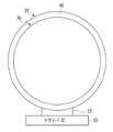
図1は、ドライバIC10、及び表示パネル20とドライバIC10と表示パネル20を連結する連結部15を含む非四角形ディスプレイの実施形態を示した図面である。表示パネル20は、非四角形の所定形態、例えば、円形、楕円形、一部が円形である多角形、または四角形を除いた多角形を有してもよい。一実施形態において、任意の形態は一部が曲線になった図形の形態を含んでもよい。表示パネル20は、少なくとも一つの曲線部を含むフレキシブル表示パネルであってもよい。 FIG. 1 is a diagram showing an embodiment of a non-rectangular display including a
表示パネル20の駆動回路を駆動するために、ドライバIC10から駆動信号が伝達される。このとき、ドライバIC10から出力される駆動信号は、連結部15を通じて表示パネル20に伝達され得る。ドライバIC10に伝達される駆動信号に基づいて、表示パネル20に形成された信号線に画素に対応する信号が適切に伝達され得る。 A drive signal is transmitted from the
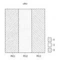
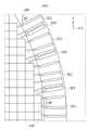
図2は、図1のディスプレイの表示パネルの実施形態を示した図面である。図2に示されているように、表示パネル20の形態または形状に基づいて、表示領域30の形態または形状が決定され得る。例えば、表示パネル20の形態が円形であれば、表示領域30の形態も円形であり得る、また、表示パネル20の一部が曲線である場合、一部に対応する表示領域30の形態も曲線の形態を有し得る。そして、表示パネル20において、表示領域30を除いた領域には、駆動回路を含む非表示領域40が位置する。 2 is a diagram illustrating an embodiment of a display panel of the display of FIG. 1. FIG. As shown in FIG. 2 , the form or shape of the
表示領域30内には複数の画素PXが位置する。画素PXは、表示領域30内にマトリックス状に配置されてもよい。このとき、画素PXは表示領域30内で曲線に対応して配置されてもよい。例えば、表示領域30の形態が円形である場合、表示領域30の周縁に位置した画素配列間に段差が発生し得る。 A plurality of pixels PX are positioned within the
例えば、一部が曲線の形態を有する表示領域30の周縁に、四角形状の画素PXが配置されるので、画素列間の段差配列を形成する。一実施形態において、第1行と第2行に対応する表示領域30の周縁CA1に、画素PXの所定個数(例えば、8個)の差ほど第1行の画素配列と第2行の画素配列間に段差が形成される。 For example, since square pixels PX are arranged along the periphery of the
行単位または列単位で隣接した画素配列間の段差は、対応する周縁の位置によって異なり得る。例えば、第1行の画素配列と第2行の画素配列間には画素8個の差ほど段差が発生するが、第2行の画素配列と第3行の画素配列間には画素6個の差ほど段差が発生し得る。 A step between adjacent pixel arrays on a row-by-row basis or a column-by-column basis may vary depending on the positions of the corresponding edges. For example, a step of 8 pixels is generated between the pixel array of the first row and the pixel array of the second row, but a step of 6 pixels is generated between the pixel array of the second row and the pixel array of the third row. Steps can occur as much as the difference.
また、駆動回路が表示領域30の形態により、非表示領域40に適切に位置する。例えば、画素PXが配置された形態が円形である場合、画素PXに信号を供給するための駆動回路が、画素PXが配置された円と隣接した周りの領域内に位置する。表示パネル20の形態が円形である場合、画素PXが配置される表示領域30及び駆動回路が配置される非表示領域40の全体が成す形態は円形であり得る。また、表示領域30と同一の基板内で表示領域30の周りに非表示領域40が形成されてもよい。 Also, the driving circuit is appropriately positioned in the
表示領域30の形態により、非表示領域40の形態が決定され得る。例えば、画素PXが配置された形態が円形である場合、非表示領域40は表示領域30の周りに所定幅を有する環(ring)形態に形成され得る。 The form of the
図2においては、すべての画素PXの形態及び大きさが同一のものと示されているが、表示領域30内部の領域を区分して配置される画素PXの大きさは異なってもよい。例えば、表示領域30の中央領域に配置される画素は、表示領域30の周縁領域(edge)に配置される画素より大きくてもよい。 In FIG. 2, all the pixels PX are shown to have the same shape and size, but the pixels PX arranged to divide the area inside the
図3は、本発明の画素PXの実施形態を示した図面であり、図4は、本発明の実施形態に関する画素PXの副画素の実施形態の等価回路図である。 FIG. 3 is a drawing showing an embodiment of the pixel PX of the present invention, and FIG. 4 is an equivalent circuit diagram of an embodiment of sub-pixels of the pixel PX according to the embodiment of the present invention.
図3に示されているように、画素PXは、互いに異なる原色で発光する複数の副画素を含んでもよい。例えば、画素PXは、それぞれ赤色(R)、緑色(G)、青色(B)で発光する3つの副画素PX11、PX12、PX13を含む。 As shown in FIG. 3, the pixel PX may include multiple sub-pixels that emit different primary colors. For example, pixel PX includes three sub-pixels PX11, PX12, and PX13 that emit red (R), green (G), and blue (B) light, respectively.
図4に示されているように、一つの副画素PX11は、複数の信号線に連結されている複数のトランジスタT1、T2、T3、T4、T5、T6、T7、ストレージキャパシタ(storage capacitor)Cst、及び有機発光ダイオード(organic light emitting diode)OLEDを含む。 As shown in FIG. 4, one subpixel PX11 includes a plurality of transistors T1, T2, T3, T4, T5, T6, and T7 connected to a plurality of signal lines, and a storage capacitor Cst. , and organic light emitting diodes (OLEDs).
トランジスタは、駆動トランジスタ(driving thin film transistor)T1、スイッチングトランジスタ(switching thin film transistor)T2、補償トランジスタT3、初期化トランジスタT4、動作制御トランジスタT5、発光制御トランジスタT6、及びバイパストランジスタT7を含む。 The transistors include a driving thin film transistor T1, a switching thin film transistor T2, a compensation transistor T3, an initialization transistor T4, an operation control transistor T5, an emission control transistor T6, and a bypass transistor T7.
信号線は、スキャン信号を伝達するスキャンラインS[n]、初期化トランジスタT4に前のスキャン信号を伝達する以前スキャンラインS[n-1]、動作制御トランジスタT5及び発光制御トランジスタT6に発光制御信号を伝達する発光制御ラインEM[n]、スキャンラインと交差して、データ信号を伝達するデータラインD[m]、電源電圧を伝達する電源電圧ライン、及び駆動トランジスタT1を初期化する初期化電圧を伝達する初期化電圧ラインを含む。 Signal lines include a scan line S[n] for transmitting a scan signal, a previous scan line S[n-1] for transmitting a previous scan signal to the initialization transistor T4, an operation control transistor T5, and a light emission control transistor T6. An emission control line EM[n] for transmitting a signal, a data line D[m] for transmitting a data signal crossing the scan line, a power voltage line for transmitting a power voltage, and an initialization for initializing the driving transistor T1. It includes an initialization voltage line that carries a voltage.
具体的に、駆動トランジスタT1は、第1ノードN1に連結される一端、第2ノードN2に連結されるゲート、及び第3ノードN3に連結される他端を含む。駆動トランジスタT1は、ゲートに印加される電圧によりターンオンされて有機発光素子OLEDに供給される駆動電流を制御する。 Specifically, the driving transistor T1 includes one end connected to the first node N1, a gate connected to the second node N2, and the other end connected to the third node N3. The driving transistor T1 is turned on by a voltage applied to its gate to control a driving current supplied to the organic light emitting device OLED.
第2トランジスタT2は、対応するデータ信号が供給されるデータラインD[m]に連結される一端、対応する本段スキャン信号が供給されるスキャンラインS[n]に連結されるゲート、及び第1ノードN1に連結される他端を含む。第2トランジスタT2は、スキャン信号によりターンオンされてデータ信号を第1ノードN1に伝達する。 The second transistor T2 has one end connected to a data line D[m] to which a corresponding data signal is supplied, a gate connected to a scan line S[n] to which a corresponding main scan signal is supplied, and a second transistor T2. It includes the other end connected to 1 node N1. The second transistor T2 is turned on by the scan signal to transmit the data signal to the first node N1.
第1キャパシタCstは、第1電源電圧ELVDDが供給される電源電圧ラインに連結される一端、及び第2ノードN2に連結される他端を含む。 The first capacitor Cst has one end connected to the power voltage line supplied with the first power voltage ELVDD and the other end connected to the second node N2.
第3トランジスタT3は、第2ノードN2に連結される一端、第3ノードN3に連結される他端、及び本段スキャンラインS[n]に連結されるゲートを含む。第3トランジスタT3は、本段スキャンライン信号によってターンオンされて第2ノードN2と第3ノードN3を連結させる。 The third transistor T3 includes one end connected to the second node N2, the other end connected to the third node N3, and a gate connected to the current scan line S[n]. The third transistor T3 is turned on by the current scan line signal to connect the second node N2 and the third node N3.
第4トランジスタT4は第2ノードN2に連結される一端、初期化電圧VINTが供給される初期化ラインに連結される他端、及び前の画素行に位置するスキャンラインS[n
-1]に連結されるゲートを含む。第4トランジスタT4は、前の画素行に位置するスキ
ャンラインS[n-1]のスキャン信号によりターンオンされて、第2ノードN2を初期化電圧VINTで初期化させる。The fourth transistor T4 has one end connected to the second node N2, the other end connected to the initialization line supplied with the initialization voltage VINT, and the scan line S[n located in the previous pixel row.
-1]. The fourth transistor T4 is turned on by the scan signal of the scan line S[n-1] located in the previous pixel row to initialize the second node N2 to the initialization voltage VINT.
第5トランジスタT5は、第1電源電圧ELVDDに連結される一端、第1ノードN1に連結される他端、及び対応する発光信号が供給される発光ラインに連結されるゲートを含む。
第5トランジスタT5は発光信号によってターンオンされる。The fifth transistor T5 includes one end connected to the first power supply voltage ELVDD, the other end connected to the first node N1, and a gate connected to the light emission line to which the corresponding light emission signal is supplied.
The fifth transistor T5 is turned on by the light emission signal.
第6トランジスタT6は、第3ノードN3に連結される一端、有機発光素子(OLED)のアノードに連結される他端、及び発光信号が供給される発光ラインに連結されるゲートを含む。第6トランジスタT6は発光信号によってターンオンされて、第1トランジスタT1を通じて流れる電流を有機発光素子OLEDに伝達する。 The sixth transistor T6 has one end connected to the third node N3, the other end connected to the anode of the organic light emitting diode (OLED), and the gate connected to the light emission line to which the light emission signal is supplied. The sixth transistor T6 is turned on by the light emission signal and transfers the current flowing through the first transistor T1 to the organic light emitting device OLED.
第7トランジスタT7は、有機発光素子OLEDのアノードに連結される一端、初期化ラインに連結される他端、及び前の画素行に位置するスキャンラインS[n-1]に連結されるゲートを含む。第7トランジスタT7は前の画素行に位置するスキャン信号によってターンオンされて、有機発光素子OLEDのアノードに初期化電圧VINTを伝達する。 The seventh transistor T7 has one end connected to the anode of the organic light emitting diode OLED, the other end connected to the initialization line, and the gate connected to the scan line S[n-1] located in the previous pixel row. include. The seventh transistor T7 is turned on by a scan signal located in the previous pixel row to transfer the initialization voltage VINT to the anode of the organic light emitting diode OLED.
有機発光素子OLEDは、第6トランジスタT6の他端に連結されるアノード、及び第2電源電圧ELVSSに連結されるカソードを含む。有機発光素子OLEDは、原色(primary color)のうちの一つの光を発光し得る。原色の例としては、赤色、緑色、青色の三原色が挙げられ、これら三原色の空間的または時間的な相互作用によって所望する色が表示され得る。 The organic light emitting device OLED includes an anode connected to the other end of the sixth transistor T6 and a cathode connected to the second power voltage ELVSS. An organic light emitting device OLED can emit light of one of primary colors. Examples of primary colors include the three primary colors red, green, and blue, and the spatial or temporal interaction of these three primary colors can display a desired color.
前の画素行に位置するスキャンラインS[n-1]を通じて供給される複数のスキャン信号に同期されて、初期化電圧Vintが複数の副画素PX11、PX12、PX13それぞれの駆動トランジスタT1のゲート電極に供給され得る。そして、本段副画素行に位置する複数のスキャンラインを通じて伝達される複数のスキャン信号に同期されて、複数のデータラインD[m]を通じて伝達される複数のデータ信号が複数の副画素PX11、PX12、PX13に伝達される。これと同時に、複数の第1電源電圧線を通じて供給される第1電源電圧ELVDDが、複数の副画素PX11、PX12、PX13を駆動させる電圧であり、複数の発光制御ラインEM[n]を通じて供給される複数の発光制御信号によって有機発光ダイオードOLEDの発光が制御される。 In synchronization with a plurality of scan signals supplied through a scan line S[n-1] located in the previous pixel row, the initialization voltage Vint is applied to the gate electrodes of the drive transistors T1 of the plurality of sub-pixels PX11, PX12, and PX13. can be supplied to Then, a plurality of data signals transmitted through a plurality of data lines D[m] are synchronized with a plurality of scan signals transmitted through a plurality of scan lines positioned in the sub-pixel row of this stage, and a plurality of data signals transmitted through a plurality of data lines D[m] are transmitted to a plurality of sub-pixels PX11, It is transmitted to PX12 and PX13. At the same time, the first power supply voltage ELVDD supplied through the plurality of first power supply voltage lines is a voltage for driving the plurality of sub-pixels PX11, PX12, and PX13, and is supplied through the plurality of emission control lines EM[n]. The light emission of the organic light emitting diode OLED is controlled by a plurality of light emission control signals.
駆動回路はスキャンラインS[n]にスキャン信号を供給する第1駆動回路、発光制御ラインEM[n]に発光制御信号を供給する第2駆動回路、及びデータラインD[m]にデータ信号を供給する第3駆動回路を含む。その他にも、駆動回路は表示パネル20の製造工程中に表示パネル20の不良有無を検査するために、テスト電圧をデータラインD[m]に供給する第4駆動回路をさらに含む。 The driving circuits include a first driving circuit that supplies a scan signal to the scan line S[n], a second driving circuit that supplies an emission control signal to the emission control line EM[n], and a data signal to the data line D[m]. and a third driver circuit for supplying the In addition, the driving circuit further includes a fourth driving circuit that supplies test voltages to the data lines D[m] in order to test whether the
前記の駆動回路は、表示パネル20内に全て配置されて対応する画素PXに適切な信号を供給する。このとき、駆動回路の種類によって画素PXに信号を供給する方法が異なる。例えば、第1駆動回路及び第2駆動回路は第1方向に信号を供給し、第3駆動回路及び第4駆動回路は第1方向と交差する第2方向に信号を供給する。画素PXがマトリックス状に配列されるとき、第1駆動回路及び第2駆動回路は行単位で信号を供給し、第3駆動回路及び第4駆動回路は列単位で信号を供給する。 The driving circuits described above are all arranged in the
このような駆動回路は、非表示領域40が表示パネル20内で狭い領域を占めるように、非表示領域40に配列される。しかし、画素PXが任意の形態に配置される表示パネル20の場合、画素配列間の段差が発生するため、画素PXが四角形に配置される表示パネル20とは異なるように駆動回路が配置されなければならない。 Such driving circuits are arranged in the
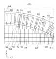
図5は、第1実施形態による表示パネル20の周縁のうちの第1位置A1に配置された画素PX及び駆動回路を示した図面である。図示されているように、駆動回路は非表示領域40に配置される。 FIG. 5 illustrates a pixel PX and a driving circuit arranged at a first position A1 on the periphery of the
以下の図面においては、第1駆動回路DC1及び第4駆動回路DC4が配置されることと説明しているが、非表示領域40内のそれぞれの位置ごとに互いに異なる種類の駆動回路(第1駆動回路、第2駆動回路、第3駆動回路及び第4駆動回路)が混合され配置されてもよい。例えば、非表示領域40には、第1駆動回路DC1と第4駆動回路DC4が混合され配置される領域、第2駆動回路DC2と第4駆動回路DC4が混合され配置される領域、第1駆動回路DC1と第3駆動回路が混合され配置される領域、及び第2駆動回路DC2と第3駆動回路が混合され配置される領域が含まれてもよい。 In the following drawings, it is explained that the first driving circuit DC1 and the fourth driving circuit DC4 are arranged, but different types of driving circuits (first driving circuit, second driving circuit, third driving circuit and fourth driving circuit) may be mixed and arranged. For example, the
そして、非表示領域40には、互いに異なる種類の駆動回路が表示領域30の周りに沿ってそれぞれの個数が異なるように配置され得る。 In the
このとき、それぞれの画素行または画素列に対応して互いに異なる種類の駆動回路が配置され得る。例えば、画素行に対応して第1駆動回路DC1が配置され、画素列に対応して第4駆動回路DC4が配置され得る。図示されているように、第1位置A1には4個の画素行に対応して第1駆動回路DC1が4個配置され、12個の画素列に対応して第4駆動回路DC4が12個配置される。 At this time, different types of driving circuits may be arranged corresponding to each pixel row or pixel column. For example, the first drive circuit DC1 can be arranged corresponding to the pixel row, and the fourth drive circuit DC4 can be arranged corresponding to the pixel column. As shown, four first driving circuits DC1 are arranged corresponding to four pixel rows at the first position A1, and twelve fourth driving circuits DC4 are arranged corresponding to twelve pixel columns. placed.
一方、互いに異なる種類の駆動回路それぞれが占める面積が互いに異なってもよい。例えば、一つの第1駆動回路DC1の面積と一つの第4駆動回路DC4の面積とが互いに異なってもよい。第1駆動回路DC1及び第4駆動回路DC4が長方形状に形成されて、互いに同一の長辺の長さを有すると、短辺の長さは異なるように形成され得る。このとき、非表示領域40の幅は、二つの駆動回路の長辺の長さの合計より小さく、一つの駆動回路の長辺の長さより大きく形成され得る。好ましくは、非表示領域40の幅がほぼ一つの駆動回路の長辺の長さと同一で、非表示領域40の幅を狭く設計できる効果がある。 On the other hand, the areas occupied by different types of driving circuits may be different from each other. For example, the area of one first drive circuit DC1 and the area of one fourth drive circuit DC4 may be different from each other. When the first driving circuit DC1 and the fourth driving circuit DC4 are formed in a rectangular shape and have the same long side length, the short side lengths may be different. At this time, the width of the
そして、駆動回路は、表示領域30の形態によって平面で対応する角度に傾いて配置され得る。具体的に、駆動回路は、表示領域30と非表示領域40の境界の法線角度とほぼ同一の角度に傾いて、非表示領域40に配置され得る。表示領域30が曲線である場合、表示領域30の周りに沿って表示領域30と非表示領域40の境界に対する法線方向が変更されるので、基準線Lrefに対する表示領域30の周りに沿って配置される駆動回路の配置角度も、前記法線方向によって変更される。図5において、最も左側に位置する第4駆動回路DC4は、基準線Lrefと平行に配置される。しかし、前記第4駆動回路DC4から表示領域30の周りに沿って右側に配置される駆動回路DC1、DC4は、基準線Lrefからの角度が次第に増加するように傾いて配置される。 In addition, the driving circuit may be inclined at a corresponding angle on the plane according to the shape of the
このとき、同じ種類の駆動回路DC4の場合においても、対応する画素行または画素列の位置によって基準線Lrefに対する配置角度α1、α2が変更される。一例として、互いに異なる画素列にそれぞれ対応する第4駆動回路DC4の配置角度α1、α2は互いに異なる。 At this time, even in the case of the same type of drive circuit DC4, the arrangement angles α1 and α2 with respect to the reference line Lref are changed depending on the position of the corresponding pixel row or pixel column. As an example, the arrangement angles α1 and α2 of the fourth drive circuits DC4 corresponding to different pixel columns are different from each other.
また、駆動回路は非表示領域40に一列に配列される。駆動回路は表示領域30の周りに沿って一列に駆動回路の種類が変更され配列される。例えば、図5において、最も左側に位置する第4駆動回路DC4から最も右側に位置する第1駆動回路DC1まで、駆動回路は表示領域30の周りに沿って一列にその種類DC1、DC4が変更され配列される。 Also, the drive circuits are arranged in a line in the
このとき、画素配列間に段差が発生する場合、当該段差の種類によって駆動回路の種類が変更され配置される。行単位で画素配列間に段差が発生すると、第1駆動回路DC1が当該段差に対応して配置され、列単位で段差が発生すると、第4駆動回路DC4が当該段差に対応して配置される。第1駆動回路DC1は互いに異なる画素行に信号を供給し、第4駆動回路DC4は互いに異なる画素列に信号を供給するためである。 At this time, if a step occurs between the pixel arrays, the type of drive circuit is changed and arranged according to the type of the step. When a step occurs between the pixel arrays in units of rows, the first driving circuit DC1 is arranged to correspond to the step, and when a step occurs in units of columns, the fourth driving circuit DC4 is arranged to correspond to the step. . This is because the first drive circuit DC1 supplies signals to different pixel rows, and the fourth drive circuit DC4 supplies signals to different pixel columns.
一つの駆動回路は、一つの行または列に含まれる画素PXに信号を供給する。一つの画素PXには複数の副画素PX11、PX12、PX13が含まれるので、一つの駆動回路は、一つの画素行または一つの画素列に含まれる複数の副画素PX11、PX12、PX13それぞれに信号を供給する。したがって、一つの駆動回路から一つの画素行または一つの画素列に供給する信号配線は複数個形成される。例えば、一つの第1駆動回路DC1は一つの画素行にスキャン信号を供給するが、一つの画素行内にはR副画素、G副画素、B副画素を含む画素PXが複数個形成されるので、複数のR副画素にスキャン信号を供給するスキャン配線SL1、複数のG副画素にスキャン信号を供給するスキャン配線SL2、及び複数のB副画素にスキャン信号を供給するスキャン配線SL3が、一つの第1駆動回路DC1と対応して形成される。これは他の種類の駆動回路DC2、DC3、DC4に連結される信号配線の場合にも同一に適用され得る。 One drive circuit supplies signals to the pixels PX included in one row or column. Since one pixel PX includes a plurality of sub-pixels PX11, PX12, and PX13, one driver circuit applies a signal to each of the plurality of sub-pixels PX11, PX12, and PX13 included in one pixel row or one pixel column. supply. Therefore, a plurality of signal wirings are formed to supply one pixel row or one pixel column from one driving circuit. For example, one first driving circuit DC1 supplies a scan signal to one pixel row, and a plurality of pixels PX including R sub-pixels, G sub-pixels, and B sub-pixels are formed in one pixel row. , a scan line SL1 that supplies scan signals to a plurality of R sub-pixels, a scan line SL2 that supplies scan signals to a plurality of G sub-pixels, and a scan line SL3 that supplies scan signals to a plurality of B sub-pixels. It is formed corresponding to the first drive circuit DC1. The same can be applied to signal lines connected to other types of driving circuits DC2, DC3, and DC4.
このとき、駆動回路が画素PXに信号を供給するための信号配線は、非表示領域40内で互いに交差しないように形成される。互いに異なる種類の駆動回路と連結された信号配線は、非表示領域40で互いに交差しないように形成される。例えば、隣接して位置した第1駆動回路DC1と画素行を連結する信号配線(SL1~SL3)と、第4駆動回路DC4と画素列を連結する信号配線TL1~TL3とは、互いに交差しないように形成される。これにより、非表示領域40内で信号配線の交差によって形成される寄生キャパシタによるカップリング(coupling)などが減少する効果がある。 At this time, the signal wirings for the driving circuit to supply signals to the pixels PX are formed so as not to cross each other within the
図6は、第1実施形態による表示パネル20の周縁のうちの第2位置A2に配置された画素PX及び駆動回路を示した図面である。図示されているように、駆動回路DC1、DC4は図5と同様に非表示領域40に配置される。そして、それぞれの画素行または画素列に対応して互いに異なる種類の駆動回路DC1、DC4が配置され得る。例えば、画素行に対応して第1駆動回路DC1が配置され、画素列に対応して第4駆動回路DC4が配置され得る。
図示されているように、第2位置A2には5個の画素行に対応して第1駆動回路DC1が5個配置され、5個の画素列に対応して第4駆動回路DC4が5個配置される。FIG. 6 is a diagram showing pixels PX and driving circuits arranged at a second position A2 on the periphery of the
As shown, at the second position A2, five first driving circuits DC1 are arranged corresponding to five pixel rows, and five fourth driving circuits DC4 are arranged corresponding to five pixel columns. placed.
そして、駆動回路DC1、DC4は、表示領域30の形態によって平面で対応する角度に傾いて配置される。図6において、基準線Lrefから時計方向に傾いた角度を測定するとき、最も左側に位置する第1駆動回路DC1が基準線Lrefから傾いた角度α3より、最も右側に位置する第4駆動回路DC4が基準線Lrefから傾いた角度α4がさらに大きい。 The driving circuits DC1 and DC4 are inclined at a corresponding angle on the plane according to the shape of the
また、駆動回路DC1、DC4は非表示領域40に一列に配列される。駆動回路DC1、DC4は表示領域30の周りに沿って一列に駆動回路の種類が変更され配列される。例えば、図6において、最も左側に位置する第4駆動回路DC4から最も右側に位置する第1駆動回路DC1まで、駆動回路は表示領域30の周りに沿って一列にその種類が変更され配列される。 Further, the driving circuits DC1 and DC4 are arranged in a line in the
このとき、画素配列間に段差が発生する場合、当該段差の種類によって駆動回路の種類が変更され配置される。行単位で画素配列間に段差が発生すると、第1駆動回路DC1が当該段差に対応して配置され、列単位で段差が発生すると、第4駆動回路DC4が当該段差に対応して配置される。第1駆動回路DC1は互いに異なる画素行に信号を供給し、第4駆動回路DC4は、互いに異なる画素列に信号を供給するためである。図6においては、行方向及び列方向に一つの画素PXほど段差が発生するので、第1駆動回路DC1と第4駆動回路DC4が交互に配置される。 At this time, if a step occurs between the pixel arrays, the type of drive circuit is changed and arranged according to the type of the step. When a step occurs between the pixel arrays in units of rows, the first driving circuit DC1 is arranged to correspond to the step, and when a step occurs in units of columns, the fourth driving circuit DC4 is arranged to correspond to the step. . This is because the first drive circuit DC1 supplies signals to different pixel rows, and the fourth drive circuit DC4 supplies signals to different pixel columns. In FIG. 6, a step difference is generated for each pixel PX in the row direction and the column direction, so the first drive circuit DC1 and the fourth drive circuit DC4 are alternately arranged.
一方、交互に配置されて、隣接するように位置する第1駆動回路DC1及び第4駆動回路DC4の表示領域30の接線方向の幅の合計は、画素PXの幅の半分以下に形成され得る。また、隣接するように位置する2個の駆動回路の幅の合計は、画素PXの幅の半分以下に形成され得る。 On the other hand, the sum of the tangential widths of the
一つの駆動回路は、一つの行または列に含まれる画素PXに信号を供給する。一つの画素PXには複数の副画素PX11、PX12、PX13が含まれるので、一つの駆動回路は、一つの画素行または一つの画素列に含まれる複数の副画素PX11、PX12、PX13それぞれに信号を供給する。したがって、一つの駆動回路から一つの画素行または一つの画素列に供給する信号配線は複数個形成される。このとき、駆動回路DC1、DC4が画素PXに信号を供給するための信号配線は、非表示領域40内で互いに交差しないように形成される。互いに異なる種類の駆動回路DC1、DC4と連結された信号配線は、非表示領域40で互いに交差しないように形成される。 One drive circuit supplies signals to the pixels PX included in one row or column. Since one pixel PX includes a plurality of sub-pixels PX11, PX12, and PX13, one driver circuit applies a signal to each of the plurality of sub-pixels PX11, PX12, and PX13 included in one pixel row or one pixel column. supply. Therefore, a plurality of signal wirings are formed to supply one pixel row or one pixel column from one driving circuit. At this time, the signal wirings for the drive circuits DC1 and DC4 to supply signals to the pixels PX are formed so as not to cross each other within the
図7は、第1実施形態による表示パネル20の周縁のうちの第3位置A3に配置された画素PX及び駆動回路を示した図面である。図示されているように、駆動回路は図5と同様に非表示領域40に配置される。そして、それぞれの画素行または画素列に対応して、互いに異なる種類の駆動回路DC1、DC4が配置され得る。例えば、画素行に対応して第1駆動回路DC1が配置され、画素列に対応して第4駆動回路DC4が配置され得る。図示されているように、第3位置A3には12個の画素行に対応して第1駆動回路DC1が12個配置され、3個の画素列に対応して第4駆動回路DC4が3個配置される。 FIG. 7 is a diagram showing pixels PX and driving circuits arranged at a third position A3 on the periphery of the
そして、駆動回路DC1、DC4は、表示領域30の形態によって平面で対応する角度に傾いて配置され得る。図7において、時計方向に傾いた角度を測定するとき、最も左側に位置する第1駆動回路DC1が基準線Lrefから傾いた角度α5より、最も右側に位置する第1駆動回路DC1が基準線Lrefから傾いた角度α6がさらに大きい。 In addition, the driving circuits DC1 and DC4 may be inclined at a corresponding angle on a plane according to the shape of the
また、駆動回路DC1、DC4は非表示領域40に一列に配列される。駆動回路DC1、DC4は表示領域30の周りに沿って一列に駆動回路の種類が変更され配列される。例えば、図7において、最も左側に位置する第1駆動回路DC1から最も右側に位置する第1駆動回路DC1まで、駆動回路は表示領域30の周りに沿って一列にその種類が変更され配列される。 Further, the driving circuits DC1 and DC4 are arranged in a line in the
このとき、画素配列間に段差が発生する場合、当該段差の種類によって駆動回路の種類が変更され配置される。行単位で画素配列間に段差が発生すると、第1駆動回路DC1が当該段差に対応して配置され、列単位で段差が発生すると、第4駆動回路DC4が当該段差に対応して配置される。第1駆動回路DC1は互いに異なる画素行に信号を供給し、第4駆動回路DC4は互いに異なる画素列に信号を供給するためである。 At this time, if a step occurs between the pixel arrays, the type of drive circuit is changed and arranged according to the type of the step. When a step occurs between the pixel arrays in units of rows, the first driving circuit DC1 is arranged to correspond to the step, and when a step occurs in units of columns, the fourth driving circuit DC4 is arranged to correspond to the step. . This is because the first drive circuit DC1 supplies signals to different pixel rows, and the fourth drive circuit DC4 supplies signals to different pixel columns.
一つの駆動回路は、一つの行または列に含まれる画素PXに信号を供給する。一つの画素PXには複数の副画素PX11、PX12、PX13が含まれるので、一つの駆動回路は、一つの画素行または一つの画素列に含まれる複数の副画素PX11、PX12、PX13それぞれに信号を供給する。したがって、一つの駆動回路から一つの画素行または一つの画素列に供給する信号配線は複数個形成される。このとき、駆動回路DC1、DC4が画素PXに信号を供給するための信号配線は、非表示領域40内で互いに交差しないように形成される。互いに異なる種類の駆動回路DC1、DC4と連結された信号配線は、非表示領域40で互いに交差しないように形成される。 One drive circuit supplies signals to the pixels PX included in one row or column. Since one pixel PX includes a plurality of sub-pixels PX11, PX12, and PX13, one driver circuit applies a signal to each of the plurality of sub-pixels PX11, PX12, and PX13 included in one pixel row or one pixel column. supply. Therefore, a plurality of signal wirings are formed to supply one pixel row or one pixel column from one driving circuit. At this time, the signal wirings for the drive circuits DC1 and DC4 to supply signals to the pixels PX are formed so as not to cross each other within the
図5乃至図7に示したように、駆動回路DC1、DC4は、表示パネル20上で配置される位置によって、その個数が異なるように配置され得る。例えば、第1位置A1では、列単位で発生する画素配列間の段差によって第4駆動回路DC4が複数個配置されるが、第3位置A3では、行単位で発生する画素配列間の段差によって第1駆動回路DC1が複数個配置される。つまり、表示領域30の周りに沿って配置される駆動回路の種類及び個数が変更される。 As shown in FIGS. 5 to 7, the driving circuits DC1 and DC4 may be arranged in different numbers depending on their positions on the
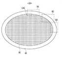
図8は、表示パネル20の第2実施形態を示した図面である。図示されているように、表示パネル20の形態に対応して表示領域30の形態が決定され得る。例えば、表示パネル20の形態が楕円形であれば、表示領域30の形態も楕円形であり得る。また、表示パネル20の一部が曲線である場合、一部に対応する表示領域30の形態も曲線の形態を有する。そして、表示パネル20において表示領域30を除いた領域には、駆動回路が配置される非表示領域40が形成される。 FIG. 8 is a drawing showing a second embodiment of the
表示領域30内には複数の画素PXが配置される。画素PXは表示領域30内にマトリックス状に配置され得る。このとき、画素PXは表示領域30内で曲線に対応して適切に配置される。例えば、表示領域30の形態が楕円形である場合、表示領域30の周縁に位置した画素配列間に段差が発生する。 A plurality of pixels PX are arranged in the
例えば、一部が曲線の形態を有する表示領域30の周縁に四角形状の画素PXが配置されるので、画素配列間の段差が発生する。例えば、第1行と第2行に対応する表示領域30の周縁CA2に、画素PX12個の差ほど第1行の画素配列と第2行の画素配列間に段差が発生する。 For example, since the square pixels PX are arranged along the periphery of the
行単位または列単位で隣接した画素配列間の段差は、対応する周縁の位置によって異なり得る。例えば、第1行の画素配列と第2行の画素配列間には画素PX12個の差ほど段差が発生するが、第2行の画素配列と第3行の画素配列間には画素PX6個の差ほど段差が発生し得る。 A step between adjacent pixel arrays on a row-by-row basis or a column-by-column basis may vary depending on the positions of the corresponding edges. For example, there is a step of 12 pixels PX between the pixel array of the first row and the pixel array of the second row, but there is a step of 6 pixels PX between the pixel array of the second row and the pixel array of the third row. Steps can occur as much as the difference.
また、駆動回路が表示領域30の形態によって非表示領域40に適切に形成される。例えば、画素PXが配置された形態が楕円形である場合、画素PXに信号を供給するための駆動回路が、画素PXが配置された楕円の周りに沿って位置する。表示パネル20の形態が楕円形である場合、画素PXが配置される表示領域30及び駆動回路が配置される非表示領域40の全体が成す形態は楕円形であり得る。 Also, the driving circuit is properly formed in the
図8において、すべての画素PXの形態及び大きさが同一のものと示されているが、表示領域30内部の領域を区分して配置される画素PXの大きさは異なってもよい。例えば、表示領域30の中央領域に配置される画素PXは、表示領域30の周縁領域(edge)に配置される画素PXより大きくてもよい。 In FIG. 8, although the shape and size of all the pixels PX are shown to be the same, the sizes of the pixels PX arranged by dividing the area inside the
このような駆動回路は、非表示領域40が表示パネル20内で狭い領域を占めるように、非表示領域40に適切に配置されなければならない。しかし、画素PXが任意の形態に配置される表示パネル20の場合、画素配列間の段差が発生するため、画素PXが四角形に配置される表示パネル20とは異なるように駆動回路が配置されなければならない。 Such driving circuits should be properly arranged in the
図9は、図8の表示パネル20の周縁のうちの第1位置に配置された画素PX及び駆動回路の実施形態を示した図面である。図示されているように、駆動回路は非表示領域40に配置される。図面には、第1駆動回路DC1及び第4駆動回路DC4が配置されることと説明しているが、非表示領域40内のそれぞれの位置ごとに互いに異なる種類の駆動回路が混合され配置されてもよい。例えば、非表示領域40には、第1駆動回路DC1と第4駆動回路DC4が混合され配置される領域、第2駆動回路と第4駆動回路DC4が混合され配置される領域、第1駆動回路DC1と第3駆動回路が混合され配置される領域、及び第2駆動回路と第3駆動回路が混合され配置される領域が含まれてもよい。そして、非表示領域40には、互いに異なる種類の駆動回路が表示領域30の周りに沿ってそれぞれの個数が異なるように配置され得る。 FIG. 9 is a diagram showing an embodiment of the pixels PX and the driving circuit arranged at the first position on the periphery of the
このとき、それぞれの画素行または画素列に対応して互いに異なる種類の駆動回路が配置され得る。例えば、画素行に対応して第1駆動回路DC1が配置され、画素列に対応して第4駆動回路DC4が配置され得る。図示されているように、第1位置には2個の画素行に対応して第1駆動回路DC1が2個配置され、10個の画素列に対応して第4駆動回路DC4が10個配置される。 At this time, different types of driving circuits may be arranged corresponding to each pixel row or pixel column. For example, the first drive circuit DC1 can be arranged corresponding to the pixel row, and the fourth drive circuit DC4 can be arranged corresponding to the pixel column. As shown, at the first position, two first driving circuits DC1 are arranged corresponding to two pixel rows, and ten fourth driving circuits DC4 are arranged corresponding to ten pixel columns. be done.
一方、互いに異なる種類の駆動回路それぞれが占める面積が互いに異なり得る。例えば、一つの第1駆動回路DC1の面積と一つの第4駆動回路DC4の面積が互いに異なり得る。 Meanwhile, areas occupied by different types of driving circuits may differ from each other. For example, the area of one first driving circuit DC1 and the area of one fourth driving circuit DC4 may be different.
そして、駆動回路DC1、DC4は、表示領域30の形態によって平面で対応する角度に傾いて配置され得る。具体的に、駆動回路は、表示領域30と非表示領域40の境界の法線角度とほぼ同一の角度に傾いて、非表示領域40に配置され得る。表示領域30が曲線である場合、表示領域30の周りに沿って表示領域30と非表示領域40の境界に対する法線方向が変更されるので、表示領域30の周りに沿って配置される駆動回路の基準線Lrefに対する配置角度も前記法線方向によって変更される。図9において、最も左側に位置する第4駆動回路DC4は基準線Lrefと平行に配置される。しかし、前記第4駆動回路DC4から表示領域30の周りに沿って右側に配置される駆動回路DC1、DC4は、基準線Lrefからの角度β1、β2が次第に増加するように傾いて配置される。 In addition, the driving circuits DC1 and DC4 may be inclined at a corresponding angle on a plane according to the shape of the
このとき、同じ種類の駆動回路の場合においても、対応する画素行または画素列の位置によって基準線Lrefに対する配置角度が変更される。一例として、互いに異なる画素行にそれぞれ対応する第1駆動回路DC1の配置角度は互いに異なる。 At this time, even in the case of the same type of drive circuit, the arrangement angle with respect to the reference line Lref is changed depending on the position of the corresponding pixel row or pixel column. As an example, the arrangement angles of the first driving circuits DC1 corresponding to different pixel rows are different from each other.
また、駆動回路DC1、DC4は非表示領域40に一列に配列される。駆動回路DC1、DC4は表示領域30の周りに沿って一列に駆動回路の種類が変更され配列される。例えば、図9において、最も左側に位置する第4駆動回路DC4から最も右側に位置する第1駆動回路DC1まで、駆動回路DC1、DC4は表示領域30の周りに沿って一列にその種類が変更され配列される。 Further, the driving circuits DC1 and DC4 are arranged in a line in the
このとき、画素配列間に段差が発生する場合、当該段差の種類によって駆動回路の種類が変更され配置される。行単位で画素配列間に段差が発生すると、第1駆動回路DC1が当該段差に対応して配置され、列単位で段差が発生すると、第4駆動回路DC4が当該段差に対応して配置される。第1駆動回路DC1は互いに異なる画素行に信号を供給し、第4駆動回路DC4は互いに異なる画素列に信号を供給するためである。 At this time, if a step occurs between the pixel arrays, the type of drive circuit is changed and arranged according to the type of the step. When a step occurs between the pixel arrays in units of rows, the first driving circuit DC1 is arranged to correspond to the step, and when a step occurs in units of columns, the fourth driving circuit DC4 is arranged to correspond to the step. . This is because the first drive circuit DC1 supplies signals to different pixel rows, and the fourth drive circuit DC4 supplies signals to different pixel columns.
一つの駆動回路は、一つの行または列に含まれる画素PXに信号を供給する。一つの画素PXには複数の副画素PX11、PX12、PX13が含まれるので、一つの駆動回路は、一つの画素行または一つの画素列に含まれる複数の副画素PX11、PX12、PX13それぞれに信号を供給する。したがって、一つの駆動回路から一つの画素行または一つの画素列に供給する信号配線は複数個形成される。例えば、一つの第1駆動回路DC1は一つの画素行にスキャン信号を供給するが、一つの画素行内にはR副画素、G副画素、B副画素を含む画素PXが複数個形成されるので、複数のR副画素にスキャン信号を供給するスキャン配線、複数のG副画素にスキャン信号を供給するスキャン配線、及び複数のB副画素にスキャン信号を供給するスキャン配線が一つの第1駆動回路DC1と対応して形成される。これは、他の種類の駆動回路に連結される信号配線の場合にも同一に適用され得る。 One drive circuit supplies signals to the pixels PX included in one row or column. Since one pixel PX includes a plurality of sub-pixels PX11, PX12, and PX13, one driver circuit applies a signal to each of the plurality of sub-pixels PX11, PX12, and PX13 included in one pixel row or one pixel column. supply. Therefore, a plurality of signal wirings are formed to supply one pixel row or one pixel column from one driving circuit. For example, one first driving circuit DC1 supplies a scan signal to one pixel row, and a plurality of pixels PX including R sub-pixels, G sub-pixels, and B sub-pixels are formed in one pixel row. , a scan wiring for supplying scan signals to a plurality of R sub-pixels, a scan wiring for supplying scan signals to a plurality of G sub-pixels, and a scan wiring for supplying scan signals to a plurality of B sub-pixels. It is formed corresponding to DC1. The same can be applied to signal wires connected to other types of driving circuits.
このとき、駆動回路DC1、DC4が画素PXに信号を供給するための信号配線は、非表示領域40内で互いに交差しないように形成される。互いに異なる種類の駆動回路と連結された信号配線は、非表示領域40で互いに交差しないように形成される。例えば、隣接して位置した第1駆動回路DC1と画素行を連結される信号配線と、第4駆動回路DC4と画素列を連結される信号配線とは、互いに交差しないように形成される。これにより、非表示領域40内で信号配線の交差によって形成される寄生キャパシタによるカップリングなどが減少する効果がある。 At this time, the signal wirings for the drive circuits DC1 and DC4 to supply signals to the pixels PX are formed so as not to cross each other within the
図10は、図8の表示パネル20の周縁のうちの第2位置に配置された画素PX及び駆動回路の実施形態を示した図面である。図示されているように、駆動回路は図9と同様に、非表示領域40に配置される。そして、それぞれの画素行または画素列に対応して互いに異なる種類の駆動回路DC1、DC4が配置され得る。例えば、画素行に対応して第1駆動回路DC1が配置され、画素列に対応して第4駆動回路DC4が配置され得る。図示されているように、第2位置には5個の画素行に対応して第1駆動回路DC1が5個配置され、5個の画素列に対応して第4駆動回路DC4が5個配置される。 FIG. 10 is a diagram showing an embodiment of the pixels PX and the driving circuit arranged at the second position on the periphery of the
そして、駆動回路DC1、DC4は、表示領域30の形態によって平面で対応する角度に傾いて配置され得る。図10において、時計方向に傾いた角度を測定するとき、最も左側に位置する第4駆動回路DC4が基準線Lrefから傾いた角度β3より、右側に位置する第1駆動回路DC1が基準線Lrefから傾いた角度β4がさらに大きい。 In addition, the driving circuits DC1 and DC4 may be inclined at a corresponding angle on a plane according to the shape of the
また、駆動回路DC1、DC4は非表示領域40に一列に配列される。駆動回路DC1、DC4は表示領域30の周りに沿って一列に駆動回路の種類が変更され配列される。例えば、図10において、最も左側に位置する第4駆動回路DC4から最も右側に位置する第1駆動回路DC1まで、駆動回路DC1、DC4は表示領域30の周りに沿って一列にその種類が変更され配列される。 Further, the driving circuits DC1 and DC4 are arranged in a line in the
このとき、画素配列間に段差が発生する場合、当該段差の種類によって駆動回路の種類が変更され配置される。行単位で画素配列間に段差が発生すると、第1駆動回路DC1が当該段差に対応して配置され、列単位で段差が発生すると、第4駆動回路DC4が当該段差に対応して配置される。第1駆動回路DC1は互いに異なる画素行に信号を供給し、第4駆動回路DC4は互いに異なる画素列に信号を供給するためである。図10においては、行方向及び列方向に一つの画素PXほど段差が発生するので、第1駆動回路DC1と第4駆動回路DC4が交互に配置される。 At this time, if a step occurs between the pixel arrays, the type of drive circuit is changed and arranged according to the type of the step. When a step occurs between the pixel arrays in units of rows, the first driving circuit DC1 is arranged to correspond to the step, and when a step occurs in units of columns, the fourth driving circuit DC4 is arranged to correspond to the step. . This is because the first drive circuit DC1 supplies signals to different pixel rows, and the fourth drive circuit DC4 supplies signals to different pixel columns. In FIG. 10, a step difference is generated by one pixel PX in the row direction and the column direction, so the first drive circuit DC1 and the fourth drive circuit DC4 are alternately arranged.
一つの駆動回路は、一つの行または列に含まれる画素PXに信号を供給する。一つの画素PXには複数の副画素PX11、PX12、PX13が含まれるので、一つの駆動回路は、一つの画素行または一つの画素列に含まれる複数の副画素PX11、PX12、PX13それぞれに信号を供給する。したがって、一つの駆動回路から一つの画素行または一つの画素列に供給する信号配線は複数個形成される。このとき、駆動回路DC1、DC4が画素PXに信号を供給するための信号配線は、非表示領域40内で互いに交差しないように形成される。互いに異なる種類の駆動回路と連結された信号配線は、非表示領域40で互いに交差しないように形成される。 One drive circuit supplies signals to the pixels PX included in one row or column. Since one pixel PX includes a plurality of sub-pixels PX11, PX12, and PX13, one driver circuit applies a signal to each of the plurality of sub-pixels PX11, PX12, and PX13 included in one pixel row or one pixel column. supply. Therefore, a plurality of signal wirings are formed to supply one pixel row or one pixel column from one driving circuit. At this time, the signal wirings for the drive circuits DC1 and DC4 to supply signals to the pixels PX are formed so as not to cross each other within the
図11は、図8の表示パネル20の周縁のうちの第3位置に配置された画素PX及び駆動回路の実施形態を示した図面である。図示されているように、駆動回路は図9と同様に、非表示領域40に配置される。そして、それぞれの画素行または画素列に対応して互いに異なる種類の駆動回路が配置され得る。例えば、画素行に対応して第1駆動回路DC1が配置され、画素列に対応して第4駆動回路DC4が配置され得る。図示されているように、第3位置には12個の画素行に対応して第1駆動回路DC1が12個配置され、3個の画素列に対応して第4駆動回路DC4が3個配置される。 FIG. 11 is a diagram showing an embodiment of the pixels PX and the driving circuit arranged at the third position on the periphery of the
そして、駆動回路DC1、DC4は、表示領域30の形態によって平面で対応する角度に傾いて配置される。図11において、時計方向に傾いた角度を測定するとき、最も左側に位置する第1駆動回路DC1が基準線Lrefから傾いた角度β5より、最も右側に位置する第1駆動回路DC1が基準線Lrefから傾いた角度β6がさらに大きい。 The driving circuits DC1 and DC4 are inclined at a corresponding angle on the plane according to the shape of the
また、駆動回路DC1、DC4は非表示領域40に一列に配列される。駆動回路DC1、DC4は表示領域30の周りに沿って一列に駆動回路の種類が変更され配列される。例えば、図11において、最も左側に位置する第1駆動回路DC1から最も右側に位置する第1駆動回路DC1まで、駆動回路DC1、DC4は表示領域30の周りに沿って一列にその種類が変更され配列される。 Further, the driving circuits DC1 and DC4 are arranged in a line in the
このとき、画素配列間に段差が発生する場合、当該段差の種類によって駆動回路の種類が変更され配置される。行単位で画素配列間に段差が発生すると、第1駆動回路DC1が当該段差に対応して配置され、列単位で段差が発生すると、第4駆動回路DC4が当該段差に対応して配置される。第1駆動回路DC1は互いに異なる画素行に信号を供給し、第4駆動回路DC4は互いに異なる画素列に信号を供給するためである。 At this time, if a step occurs between the pixel arrays, the type of drive circuit is changed and arranged according to the type of the step. When a step occurs between the pixel arrays in units of rows, the first driving circuit DC1 is arranged to correspond to the step, and when a step occurs in units of columns, the fourth driving circuit DC4 is arranged to correspond to the step. . This is because the first drive circuit DC1 supplies signals to different pixel rows, and the fourth drive circuit DC4 supplies signals to different pixel columns.
一つの駆動回路は、一つの行または列に含まれる画素PXに信号を供給する。一つの画素PXには複数の副画素PX11、PX12、PX13が含まれるので、一つの駆動回路は、一つの画素行または一つの画素列に含まれる複数の副画素PX11、PX12、PX13それぞれに信号を供給する。したがって、一つの駆動回路から一つの画素行または一つの画素列に供給する信号配線は複数個形成される。このとき、駆動回路DC1、DC4が画素PXに信号を供給するための信号配線は、非表示領域40内で互いに交差しないように形成される。互いに異なる種類の駆動回路と連結された信号配線は、非表示領域40で互いに交差しないように形成される。 One drive circuit supplies signals to the pixels PX included in one row or column. Since one pixel PX includes a plurality of sub-pixels PX11, PX12, and PX13, one driver circuit applies a signal to each of the plurality of sub-pixels PX11, PX12, and PX13 included in one pixel row or one pixel column. supply. Therefore, a plurality of signal wirings are formed to supply one pixel row or one pixel column from one driving circuit. At this time, the signal wirings for the drive circuits DC1 and DC4 to supply signals to the pixels PX are formed so as not to cross each other within the
図9乃至図11に示されているように、駆動回路DC1、DC4は、表示パネル20上で配置される位置によって、その個数が異なるように配置される。例えば、第1位置では、列単位で発生する画素配列間の段差によって第4駆動回路DC4が複数個配置されるが、第3位置では、行単位で発生する画素配列間の段差によって第1駆動回路DC1が複数個配置される。つまり、表示領域30の周りに沿って配置される駆動回路DC1、DC4の種類及び個数が変更される。 As shown in FIGS. 9 to 11, the drive circuits DC1 and DC4 are arranged in different numbers depending on the position on the
また、第1実施形態と比較して、第2実施形態の場合、表示領域30が楕円形に形成されて、表示領域30と非表示領域40の境界線の曲率が変更される。しかし、実施形態によれば、駆動回路DC1、DC4が表示領域30の周りに沿って一列に配列され、表示領域30と非表示領域40の境界線の法線方向に配置されるので、曲率が変更される場合にも非表示領域40の幅を縮小させる効果がある。 Further, in the case of the second embodiment, the
図12は、表示パネル20の第3実施形態を示した図面である。図示されているように、表示パネル20は一部が曲線に形成され得る。例えば、表示パネル20は、弓形状の第1領域CA3及び四角形状の第2領域CA4が結合される形態であり得る。 FIG. 12 is a drawing showing a third embodiment of the
表示パネル20の形態に対応して表示領域30の形態が決定され得る。例えば、表示パネル20の一部が曲線である場合、一部に対応する表示領域30の形態も曲線の形態を有する。
したがって、第1領域CA3の表示領域30は弓形状に形成され、第2領域CA4の表示領域30は四角形状に形成される。そして、表示パネル20において表示領域30を除いた領域には、駆動回路が配置される非表示領域40が形成される。The form of the
Therefore, the
表示領域30内には複数の画素PXが配置される。画素PXは表示領域30内にマトリックス状に配置され得る。このとき、画素PXは、表示領域30内で曲線に対応して適切に配置される。例えば、表示領域30が弓形状である場合、弓形状の表示領域30の周縁に位置した画素配列間に段差が発生する。 A plurality of pixels PX are arranged in the
つまり、一部が曲線の形態を有する表示領域30の周縁に四角形状の画素PXが配置されるので、画素配列間の段差が発生する。例えば、第1行と第2行に対応する表示領域30の周縁に、画素PX6個の差ほど第1行の画素配列と第2行の画素配列間に段差が発生する。 That is, since the square pixels PX are arranged along the periphery of the
行単位または列単位で隣接した画素配列間の段差は、対応する周縁の位置によって異なり得る。例えば、第1行の画素配列と第2行の画素配列間には画素PX6個の差ほど段差が発生するが、第2行の画素配列と第3行の画素配列間には画素PX4個の差ほど段差が発生し得る。 A step between adjacent pixel arrays on a row-by-row basis or a column-by-column basis may vary depending on the positions of the corresponding edges. For example, a step of 6 pixels PX is generated between the pixel array of the first row and the pixel array of the second row, but a step of 4 pixels PX is generated between the pixel array of the second row and the pixel array of the third row. Steps can occur as much as the difference.
また、駆動回路が表示領域30の形態によって非表示領域40に適切に形成される。例えば、画素PXが配置された形態が弓形状である場合、画素PXに信号を供給するための駆動回路が、画素PXが配置された弓形の弧の周りに沿って位置する。表示パネル20の形態が弓形状である場合、画素PXが配置される表示領域30及び駆動回路が配置される非表示領域40全体が成す形態が弓形状であり得る。 Also, the driving circuit is properly formed in the
図12においては、すべての画素PXの形態及び大きさが同一のものと示されているが、表示領域30内部の領域を区分して配置される画素PXの大きさは異なり得る。例えば、表示領域30の第2領域CA4に配置される画素PXは、第1領域CA3の周縁領域(edge)に配置される画素PXより大きくてもよい。 Although FIG. 12 shows that all the pixels PX have the same shape and size, the pixels PX arranged to divide the area inside the
このような駆動回路DC1、DC2、DC4は、非表示領域40が表示パネル20内で狭い領域を占めるように、非表示領域40に適切に配置されなければならない。しかし、画素PXが任意の形態に配置される表示パネル20の場合、画素配列間の段差が発生するため、画素PXが四角形に配置される表示パネル20とは異なるように駆動回路が配置されなければならない。 Such driving circuits DC1, DC2, DC4 must be properly arranged in the
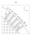
図13は、図12の表示パネル20の第1領域CA3の周縁のうちの第1位置に配置された画素PX及び駆動回路の実施形態を示した図面である。図示されているように、駆動回路は非表示領域40に配置される。図面には、第1駆動回路DC1、第2駆動回路DC2及び第4駆動回路DC4が配置されることと説明されているが、非表示領域40内のそれぞれの位置ごとに互いに異なる種類の駆動回路DC1、DC2、DC4が混合され配置され得る。
例えば、非表示領域40には、第1駆動回路DC1、第2駆動回路DC2及び第4駆動回路DC4が混合され配置される領域、第1駆動回路DC1と第4駆動回路DC4が混合され配置される領域、第2駆動回路DC2と第4駆動回路DC4が混合され配置される領域が含まれてもよい。そして、非表示領域40には互いに異なる種類の駆動回路DC1、DC2、DC4が、表示領域30の周りに沿ってそれぞれの個数が異なるように配置され得る。FIG. 13 is a diagram showing an embodiment of the pixels PX and the driving circuit arranged at the first position on the periphery of the first area CA3 of the
For example, in the
このとき、それぞれの画素行または画素列に対応して互いに異なる種類の駆動回路DC1、DC2、DC4が配置され得る。例えば、画素行に対応して第1駆動回路DC1及び第2駆動回路DC2が配置され、画素列に対応して第4駆動回路DC4が配置され得る。図示されているように、第1位置には、1個の画素行に対応して第1駆動回路DC1及び第2駆動回路DC2が一つずつ配置され、14個の画素列に対応して第4駆動回路DC4が14個配置される。 At this time, different types of driving circuits DC1, DC2, and DC4 may be arranged corresponding to each pixel row or pixel column. For example, a first drive circuit DC1 and a second drive circuit DC2 may be arranged corresponding to pixel rows, and a fourth drive circuit DC4 may be arranged corresponding to pixel columns. As shown, at the first position, one first driving circuit DC1 and one second driving circuit DC2 are arranged corresponding to one pixel row, and a second driving circuit DC1 is arranged corresponding to 14 pixel columns. Fourteen 4-drive circuits DC4 are arranged.
一方、互いに異なる種類の駆動回路DC1、DC2、DC4それぞれが占める面積が互いに異なってもよい。例えば、一つの第1駆動回路DC1の面積、一つの第2駆動回路DC2の面積、及び一つの第4駆動回路DC4の面積が互いに異なってもよい。 On the other hand, the areas occupied by the different types of drive circuits DC1, DC2, and DC4 may be different from each other. For example, the area of one first drive circuit DC1, the area of one second drive circuit DC2, and the area of one fourth drive circuit DC4 may be different from each other.
そして、駆動回路DC1、DC2、DC4は、表示領域30の形態によって平面で対応する角度に傾いて配置され得る。具体的に、駆動回路は、第1領域CA3で表示領域30と非表示領域40の境界の法線角度とほぼ同一の角度に傾いて、非表示領域40に配置され得る。表示領域30が曲線である場合、表示領域30の周りに沿って表示領域30と非表示領域40の境界に対する法線方向が変更されるので、表示領域30の周りに沿って配置される駆動回路の基準線Lrefに対する配置角度も前記法線方向によって変更される。図13で中央に位置する第4駆動回路DC4は、基準線Lrefと平行に配置される。しかし、前記第4駆動回路DC4から表示領域30の周りに沿って右側または左側に配置される駆動回路DC1、DC2、DC4は、基準線Lrefからの角度が次第に増加するか、または減少するように傾いて配置される。例えば、右側に配置される第4駆動回路DC4の基準線Lrefからの配置角度γ1は、正の値を有する。 In addition, the driving circuits DC1, DC2, and DC4 may be inclined at a corresponding angle on a plane according to the shape of the
このとき、同じ種類の駆動回路の場合にも、対応する画素行または画素列の位置によって基準線Lrefに対する配置角度が変更される。一例として、互いに異なる画素列にそれぞれ対応する第4駆動回路DC4の配置角度は互いに異なる。 At this time, the arrangement angle with respect to the reference line Lref is changed depending on the position of the corresponding pixel row or pixel column even in the case of the same type of drive circuit. As an example, the arrangement angles of the fourth driving circuits DC4 corresponding to different pixel columns are different from each other.
また、駆動回路DC1、DC2、DC4は非表示領域40に一列に配列される。駆動回路DC1、DC2、DC4は表示領域30の周りに沿って一列に駆動回路の種類が変更され配列される。例えば、図13において、最も左側に位置する第2駆動回路DC2から最も右側に位置する第1駆動回路DC1まで、駆動回路DC1、DC2、DC4は表示領域30の周りに沿って一列にその種類が変更され配列される。 In addition, the drive circuits DC1, DC2 and DC4 are arranged in a line in the
このとき、画素配列間に段差が発生する場合、当該段差の種類によって駆動回路の種類が変更され配置される。行単位で画素配列間に段差が発生すると、第1駆動回路DC1及び第2駆動回路DC2が当該段差に対応して配置され、列単位で段差が発生すると、第4駆動回路DC4が当該段差に対応して配置される。第1駆動回路DC1及び第2駆動回路DC2は互いに異なる画素行に信号を供給し、第4駆動回路DC4は互いに異なる画素列に信号を供給するためである。 At this time, if a step occurs between the pixel arrays, the type of drive circuit is changed and arranged according to the type of the step. When a step occurs between the pixel arrays in units of rows, the first drive circuit DC1 and the second drive circuit DC2 are arranged to correspond to the step. arranged correspondingly. This is because the first driving circuit DC1 and the second driving circuit DC2 supply signals to different pixel rows, and the fourth driving circuit DC4 supplies signals to different pixel columns.
このとき、第1駆動回路DC1及び第2駆動回路DC2は、同一の行単位で発生する画素配列間の段差に対応して隣接した領域に配置されてもよい。または、図13に示されているように、第1画素行と第2画素行の段差は、中央領域の左側及び右側で発生するので、左側または右側に対応して第1駆動回路DC1及び第2駆動回路DC2が配置され得る。つまり、左側の第1画素行及び第2画素行の段差に対応して第2駆動回路DC2が配置され、右側の第1画素行及び第2画素行の段差に対応して第1駆動回路DC1が配置され得る。 At this time, the first driving circuit DC1 and the second driving circuit DC2 may be arranged in adjacent regions corresponding to steps between pixel arrays that occur in the same row unit. Alternatively, as shown in FIG. 13, the steps between the first pixel row and the second pixel row occur on the left and right sides of the central region, so that the first driving circuit DC1 and the second driving circuit DC1 correspond to the left or right side. 2 drive circuits DC2 can be arranged. That is, the second drive circuit DC2 is arranged corresponding to the steps of the first and second pixel rows on the left side, and the first drive circuit DC1 is arranged corresponding to the steps of the first and second pixel rows on the right side. can be placed.
一つの駆動回路は、一つの行または列に含まれる画素PXに信号を供給する。一つの画素PXには複数の副画素PX11、PX12、PX13が含まれるので、一つの駆動回路は、一つの画素行または一つの画素列に含まれる複数の副画素PX11、PX12、PX13それぞれに信号を供給する。したがって、一つの駆動回路から一つの画素行または一つの画素列に供給する信号配線は複数個形成される。例えば、一つの第1駆動回路DC1は一つの画素行にスキャン信号を供給するが、一つの画素行内にはR副画素、G副画素、B副画素を含む画素PXが複数個形成されるので、複数のR副画素にスキャン信号を供給するスキャン配線、複数のG副画素にスキャン信号を供給するスキャン配線、及び複数のB副画素にスキャン信号を供給するスキャン配線が一つの第1駆動回路DC1と対応して形成される。これは、他の種類の駆動回路に連結される信号配線の場合にも同一に適用され得る。 One drive circuit supplies signals to the pixels PX included in one row or column. Since one pixel PX includes a plurality of sub-pixels PX11, PX12, and PX13, one driver circuit applies a signal to each of the plurality of sub-pixels PX11, PX12, and PX13 included in one pixel row or one pixel column. supply. Therefore, a plurality of signal wirings are formed to supply one pixel row or one pixel column from one driving circuit. For example, one first driving circuit DC1 supplies a scan signal to one pixel row, and a plurality of pixels PX including R sub-pixels, G sub-pixels, and B sub-pixels are formed in one pixel row. , a scan wiring for supplying scan signals to a plurality of R sub-pixels, a scan wiring for supplying scan signals to a plurality of G sub-pixels, and a scan wiring for supplying scan signals to a plurality of B sub-pixels. It is formed corresponding to DC1. The same can be applied to signal wires connected to other types of driving circuits.
このとき、駆動回路DC1、DC2、DC4が画素PXに信号を供給するための信号配線は、非表示領域40内で互いに交差しないように形成される。互いに異なる種類の駆動回路DC1、DC2、DC4と連結された信号配線は、非表示領域40で互いに交差しないように形成される。例えば、隣接するように位置した第1駆動回路DC1と画素行を連結される信号配線と、第4駆動回路DC4と画素列を連結される信号配線とは、互いに交差しないように形成される。これにより、非表示領域40内で信号配線の交差によって形成される寄生キャパシタによるカップリングなどが減少する効果がある。 At this time, the signal wirings for the drive circuits DC1, DC2, and DC4 to supply signals to the pixels PX are formed so as not to cross each other within the
図14は、図12の表示パネル20の第1領域CA3の周縁のうちの第2位置に配置された画素PX及び駆動回路の実施形態を示した図面である。図示されているように、駆動回路は図13と同様に、非表示領域40に配置される。そして、それぞれの画素行または画素列に対応して互いに異なる種類の駆動回路DC1、DC2、DC4が配置され得る。例えば、画素行に対応して第1駆動回路DC1が配置され、画素列に対応して第4駆動回路DC4が配置され得る。図示されているように、第2位置には4個の画素行に対応して第1駆動回路DC1が4個配置され、6個の画素列に対応して第4駆動回路DC4が6個配置される。 FIG. 14 is a diagram showing an embodiment of the pixels PX and the driving circuit arranged at the second position on the periphery of the first area CA3 of the
そして、駆動回路DC1、DC2、DC4は、表示領域30の形態によって平面で対応する角度に傾いて配置され得る。図14において、時計方向に傾いた角度を測定するとき、最も左側に位置する第1駆動回路DC1が基準線Lrefから傾いた角度より、最も右側に位置する第4駆動回路DC4が基準線Lrefから傾いた角度がさらに大きい。 In addition, the driving circuits DC1, DC2, and DC4 may be inclined at a corresponding angle on a plane according to the shape of the
また、駆動回路DC1、DC2、DC4は非表示領域40に一列に配列される。駆動回路DC1、DC2、DC4は表示領域30の周りに沿って一列に駆動回路の種類が変更され配列される。例えば、図14において、最も左側に位置する第4駆動回路DC4から最も右側に位置する第1駆動回路DC1まで、駆動回路DC1、DC2、DC4は表示領域30の周りに沿って一列にその種類が変更され配列される。 In addition, the drive circuits DC1, DC2 and DC4 are arranged in a line in the
このとき、画素配列間に段差が発生する場合、当該段差の種類によって駆動回路の種類が変更され配置される。行単位で画素配列間に段差が発生すると、第1駆動回路DC1が当該段差に対応して配置され、列単位で段差が発生すると、第4駆動回路DC4が当該段差に対応して配置される。第1駆動回路DC1は互いに異なる画素行に信号を供給し、第4駆動回路DC4は互いに異なる画素列に信号を供給するためである。図14では、行方向及び列方向に一つの画素PXほど段差が発生するので、第1駆動回路DC1と第4駆動回路DC4が交互に配置される。 At this time, if a step occurs between the pixel arrays, the type of drive circuit is changed and arranged according to the type of the step. When a step occurs between the pixel arrays in units of rows, the first driving circuit DC1 is arranged to correspond to the step, and when a step occurs in units of columns, the fourth driving circuit DC4 is arranged to correspond to the step. . This is because the first drive circuit DC1 supplies signals to different pixel rows, and the fourth drive circuit DC4 supplies signals to different pixel columns. In FIG. 14, a step difference is generated by one pixel PX in the row direction and the column direction, so the first drive circuit DC1 and the fourth drive circuit DC4 are alternately arranged.
一つの駆動回路は、一つの行または列に含まれる画素PXに信号を供給する。一つの画素PXには複数の副画素PX11、PX12、PX13が含まれるので、一つの駆動回路は、一つの画素行または一つの画素列に含まれる複数の副画素PX11、PX12、PX13それぞれに信号を供給する。したがって、一つの駆動回路から一つの画素行または一つの画素列に供給する信号配線は複数個形成される。このとき、駆動回路DC1、DC2、DC4が画素PXに信号を供給するための信号配線は、非表示領域40内で互いに交差しないように形成される。互いに異なる種類の駆動回路DC1、DC2、DC4と連結された信号配線は、非表示領域40で互いに交差しないように形成される。 One drive circuit supplies signals to the pixels PX included in one row or column. Since one pixel PX includes a plurality of sub-pixels PX11, PX12, and PX13, one driver circuit applies a signal to each of the plurality of sub-pixels PX11, PX12, and PX13 included in one pixel row or one pixel column. supply. Therefore, a plurality of signal wirings are formed to supply one pixel row or one pixel column from one driving circuit. At this time, the signal wirings for the drive circuits DC1, DC2, and DC4 to supply signals to the pixels PX are formed so as not to cross each other within the
図15は、図12の表示パネル20の第1領域CA3の周縁のうちの第3位置に配置された画素PX及び駆動回路の実施形態を示した図面である。図示されているように、駆動回路は図13と同様に、非表示領域40に配置される。そして、それぞれの画素行または画素列に対応して互いに異なる種類の駆動回路DC1、DC2、DC4が配置され得る。例えば、画素行に対応して第2駆動回路DC2が配置され、画素列に対応して第4駆動回路DC4が配置され得る。図示されているように、第3位置には4個の画素行に対応して第2駆動回路DC2が4個配置され、6個の画素列に対応して第4駆動回路DC4が6個配置される。 FIG. 15 is a view showing an embodiment of the pixels PX and the driving circuit arranged at the third position on the periphery of the first area CA3 of the
第3位置は、第2位置と表示領域30の中央領域を基準として対称であり、第2位置の非表示領域40には第1駆動回路DC1及び第4駆動回路DC4が配置されるが、第3位置の非表示領域40には第2駆動回路DC2及び第4駆動回路DC4が配置され得る。 The third position is symmetrical to the second position with respect to the center area of the
そして、駆動回路DC1、DC2、DC4は、表示領域30の形態によって平面で対応する角度に傾いて配置され得る。図15において、基準線Lrefから時計方向に傾いた角度を測定するとき、最も左側に位置する第2駆動回路DC2が基準線Lrefから傾いた角度より、最も右側に位置する第4駆動回路DC4が基準線Lrefから傾いた角度がさらに大きい。 In addition, the driving circuits DC1, DC2, and DC4 may be inclined at a corresponding angle on a plane according to the shape of the
また、駆動回路DC1、DC2、DC4は非表示領域40に一列に配列される。駆動回路DC1、DC2、DC4は表示領域30の周りに沿って一列に駆動回路の種類が変更され配列される。例えば、図15において、最も左側に位置する第2駆動回路DC2から最も右側に位置する第4駆動回路DC4まで、駆動回路DC1、DC2、DC4は表示領域30の周りに沿って一列にその種類が変更され配列される。 In addition, the drive circuits DC1, DC2 and DC4 are arranged in a line in the
このとき、画素配列間に段差が発生する場合、当該段差の種類によって駆動回路の種類が変更され配置される。行単位で画素配列間に段差が発生すると、第2駆動回路DC2が当該段差に対応して配置され、列単位で段差が発生すると、第4駆動回路DC4が当該段差に対応して配置される。第2駆動回路DC2は互いに異なる画素行に信号を供給し、第4駆動回路DC4は互いに異なる画素列に信号を供給するためである。 At this time, if a step occurs between the pixel arrays, the type of drive circuit is changed and arranged according to the type of the step. When a step occurs between the pixel arrays in units of rows, the second drive circuit DC2 is arranged corresponding to the step, and when a step occurs in units of columns, the fourth drive circuit DC4 is arranged corresponding to the step. . This is because the second drive circuit DC2 supplies signals to different pixel rows, and the fourth drive circuit DC4 supplies signals to different pixel columns.
一つの駆動回路は、一つの行または列に含まれる画素PXに信号を供給する。一つの画素PXには複数の副画素PX11、PX12、PX13が含まれるので、一つの駆動回路は、一つの画素行または一つの画素列に含まれる複数の副画素PX11、PX12、PX13それぞれに信号を供給する。したがって、一つの駆動回路から一つの画素行または一つの画素列に供給する信号配線は複数個形成される。このとき、駆動回路DC1、DC2、DC4が画素PXに信号を供給するための信号配線は、非表示領域40内で互いに交差しないように形成される。互いに異なる種類の駆動回路DC1、DC2、DC4と連結された信号配線は、非表示領域40で互いに交差しないように形成される。 One drive circuit supplies signals to the pixels PX included in one row or column. Since one pixel PX includes a plurality of sub-pixels PX11, PX12, and PX13, one driver circuit applies a signal to each of the plurality of sub-pixels PX11, PX12, and PX13 included in one pixel row or one pixel column. supply. Therefore, a plurality of signal wirings are formed to supply one pixel row or one pixel column from one driving circuit. At this time, the signal wirings for the drive circuits DC1, DC2, and DC4 to supply signals to the pixels PX are formed so as not to cross each other within the
図13乃至図15に示されているように、駆動回路DC1、DC2、DC4は、表示パネル20上で配置される位置によって、その個数が異なるように配置され得る。例えば、第1位置では、列単位で発生する画素配列間の段差によって第4駆動回路DC4が複数個配置されるが、第2位置では、行単位で発生する画素配列間の段差によって第1駆動回路DC1が複数個配置され、第3位置では行単位で発生する画素配列間の段差によって第2駆動回路DC2が複数個配置される。つまり、表示領域30の周りに沿って配置される駆動回路DC1、DC2、DC4の種類及び個数が変更される。 As shown in FIGS. 13 to 15, the number of driving circuits DC1, DC2, and DC4 may vary depending on the positions on the
また、第1実施形態及び第2実施形態と比較して、第3実施形態の場合、表示領域30の一部が弓形に形成されて、表示領域30と非表示領域40の境界線の曲率が変更される。しかし、実施形態によれば、駆動回路DC1、DC2、DC4が表示領域30の周りに沿って一列に配列され、表示領域30と非表示領域40の境界線の法線方向に配置されるので、曲率が変更される場合にも非表示領域40の幅を縮小させる効果がある。 Further, in comparison with the first and second embodiments, in the case of the third embodiment, a part of the
図16は、表示パネル20の第4実施形態を示した図面である。図示されているように、表示パネル20は一部が曲線に形成され得る。例えば、表示パネル20は、凹曲線状の第1領域CA5及び四角形状の第2領域CA6が結合される形態であり得る。 FIG. 16 is a drawing showing a fourth embodiment of the
表示パネル20の形態に対応して表示領域30の形態が決定され得る。例えば、表示パネル20の一部が曲線である場合、一部に対応する表示領域30の形態も曲線の形態を有する。
したがって、第1領域CA5の表示領域30は凹曲線状に形成され、第2領域CA6の表示領域30は四角形状に形成される。そして、表示パネル20において表示領域30を除いた領域には、駆動回路が配置される非表示領域40が形成される。The form of the
Therefore, the
表示領域30内には複数の画素PXが配置される。画素PXは表示領域30内にマトリックス状に配置され得る。このとき、画素PXは表示領域30内で曲線に対応して適切に配置される。例えば、表示領域30が凹曲線状である場合、凹曲線状の表示領域30の周縁に位置した画素配列間に段差が発生する。 A plurality of pixels PX are arranged in the
つまり、一部が曲線の形態を有する表示領域30の周縁に四角形状の画素PXが配置されるので、画素配列間の段差が発生する。例えば、左側から第1列と第2列に対応する表示領域30の周縁に、画素PX2個の差ほど第1列の画素配列と第2列の画素配列間に段差が発生する。 That is, since the square pixels PX are arranged along the periphery of the
行単位または列単位で隣接した画素配列間の段差は、対応する周縁の位置によって異なってもよい。例えば、第1列の画素配列と第2列の画素配列間には画素PX2個の差ほど段差が発生するが、第3列の画素配列と第4列の画素配列間には画素PX1個の差ほど段差が発生し得る。 A step between adjacent pixel arrays in a row unit or a column unit may differ according to the position of the corresponding edge. For example, a step of two pixels PX occurs between the pixel array of the first column and the pixel array of the second column, but a step of one pixel PX occurs between the pixel array of the third column and the pixel array of the fourth column. Steps can occur as much as the difference.
また、駆動回路が表示領域30の形態によって非表示領域40に適切に形成される。例えば、画素PXが配置された形態が凹曲線状である場合、画素PXに信号を供給するための駆動回路が、画素PXが配置された凹曲線に沿って位置する。 Also, the driving circuit is properly formed in the
図16においては、すべての画素PXの形態及び大きさが同一のものと示されているが、表示領域30内部の領域を区分して配置される画素PXの大きさは異なってもよい。例えば、表示領域30の第2領域CA6に配置される画素PXは、第1領域CA5の周縁領域(edge)に配置される画素PXより大きくてもよい。 In FIG. 16, all the pixels PX are shown to have the same shape and size, but the pixels PX arranged to divide the area inside the
このような駆動回路DC1、DC2、DC4は、非表示領域40が表示パネル20内で狭い領域を占めるように、非表示領域40に適切に配置されなければならない。しかし、画素PXが任意の形態に配置される表示パネル20の場合、画素配列間の段差が発生するため、画素PXが四角形に配置される表示パネル20とは異なるように駆動回路が配置されなければならない。これについて、図17を参照して、第4実施形態による表示パネル20の駆動回路配置について説明する。 Such driving circuits DC1, DC2, DC4 must be properly arranged in the
図17は、図16の表示パネル20の第1領域CA5の第1位置D1に配置された画素PX及び駆動回路の実施形態を示した図面である。図示されているように、駆動回路は非表示領域40に配置される。図面には、第1駆動回路DC1、第2駆動回路DC2及び第4駆動回路DC4が配置されることと説明したが、非表示領域40内のそれぞれの位置ごとに互いに異なる種類の駆動回路DC1、DC2、DC4が混合され配置され得る。例えば、非表示領域40には、第1駆動回路DC1及び第4駆動回路DC4が混合され配置される領域、第2駆動回路DC2が配置される領域、第3駆動回路が配置される領域が含まれてもよい。そして、非表示領域40には、互いに異なる種類の駆動回路DC1、DC2、DC4が表示領域30の周りに沿ってそれぞれの個数が異なるように配置され得る。 FIG. 17 is a drawing showing an embodiment of the pixel PX and the driving circuit arranged at the first position D1 of the first area CA5 of the
このとき、それぞれの画素行または画素列に対応して、互いに異なる種類の駆動回路DC1、DC2、DC4が配置され得る。例えば、画素行に対応して第1駆動回路DC1及び第2駆動回路DC2が配置され、画素列に対応して第4駆動回路DC4が配置され得る。図示されているように、第1領域CA5には、7個の画素行に対応して第1駆動回路DC1及び第2駆動回路DC2がそれぞれ7個配置され、5個の画素列に対応して第4駆動回路DC4が5個配置される。 At this time, different types of drive circuits DC1, DC2, and DC4 may be arranged corresponding to the respective pixel rows or pixel columns. For example, a first drive circuit DC1 and a second drive circuit DC2 may be arranged corresponding to pixel rows, and a fourth drive circuit DC4 may be arranged corresponding to pixel columns. As shown, in the first area CA5, seven first drive circuits DC1 and seven second drive circuits DC2 are arranged corresponding to seven pixel rows, and seven drive circuits DC2 are arranged corresponding to five pixel columns. Five fourth drive circuits DC4 are arranged.
一方、互いに異なる種類の駆動回路DC1、DC2、DC4それぞれが占める面積が互いに異なってもよい。例えば、一つの第1駆動回路DC1の面積、一つの第2駆動回路DC2の面積、及び一つの第4駆動回路DC4の面積が互いに異なってもよい。 On the other hand, the areas occupied by the different types of drive circuits DC1, DC2, and DC4 may be different from each other. For example, the area of one first drive circuit DC1, the area of one second drive circuit DC2, and the area of one fourth drive circuit DC4 may be different from each other.
そして、駆動回路DC1、DC2、DC4は、表示領域30の形態によって平面で対応する角度に傾いて配置され得る。具体的に、駆動回路は第1領域CA5で表示領域30と非表示領域40の境界の法線角度とほぼ同一の角度に傾いて、非表示領域40に配置され得る。表示領域30が曲線である場合、曲線の表示領域30の周りに沿って表示領域30と非表示領域40の境界に対する法線方向が変更されるので、表示領域30の周りに沿って配置される駆動回路の基準線Lrefに対する配置角度も前記法線方向によって変更される。 In addition, the driving circuits DC1, DC2, and DC4 may be inclined at a corresponding angle on a plane according to the shape of the
図17において、表示領域30の左側に位置する第2駆動回路DC2は、対応する表示領域30の形態が直線であるため、直線と直交する角度に配置される。そして、表示領域30の最も左側画素列と連結される第4駆動回路DC4から、表示領域30の周りに沿って右側に配置される駆動回路DC1、DC2、DC4は、基準線Lrefからの角度が次第に減少するように傾いて配置される。例えば、最も左側の画素列と連結される第4駆動回路DC4の基準線Lrefからの配置角度δ1は、正の値を有する。 In FIG. 17, the second driving circuit DC2 located on the left side of the
このとき、同じ種類の駆動回路の場合にも、対応する画素行または画素列の位置によって基準線Lrefに対する配置角度が変更される。一例として、互いに異なる画素列にそれぞれ対応する第4駆動回路DC4の配置角度は互いに異なる。 At this time, the arrangement angle with respect to the reference line Lref is changed depending on the position of the corresponding pixel row or pixel column even in the case of the same type of drive circuit. As an example, the arrangement angles of the fourth driving circuits DC4 corresponding to different pixel columns are different from each other.
また、駆動回路DC1、DC2、DC4は非表示領域40に一列に配列される。駆動回路DC1、DC2、DC4は表示領域30の周りに沿って一列に駆動回路の種類が変更され配列される。例えば、図17に示されているように、曲線形態の表示領域30に対応して、最も左側に位置する第4駆動回路DC4から最も右側に位置する第1駆動回路DC1まで、駆動回路DC1、DC2、DC4は表示領域30の周りに沿って一列にその種類が変更され配列される。 In addition, the drive circuits DC1, DC2 and DC4 are arranged in a line in the
このとき、画素配列間に段差が発生する場合、当該段差の種類によって駆動回路の種類が変更され配置される。行単位で画素配列間に段差が発生すると、第1駆動回路DC1及び第2駆動回路DC2が当該段差に対応して配置され、列単位で段差が発生すると、第4駆動回路DC4が当該段差に対応して配置される。第1駆動回路DC1及び第2駆動回路DC2は互いに異なる画素行に信号を供給し、第4駆動回路DC4は互いに異なる画素列に信号を供給するためである。 At this time, if a step occurs between the pixel arrays, the type of drive circuit is changed and arranged according to the type of the step. When a step occurs between the pixel arrays in units of rows, the first drive circuit DC1 and the second drive circuit DC2 are arranged to correspond to the step. arranged correspondingly. This is because the first driving circuit DC1 and the second driving circuit DC2 supply signals to different pixel rows, and the fourth driving circuit DC4 supplies signals to different pixel columns.
一つの駆動回路は、一つの行または列に含まれる画素PXに信号を供給する。一つの画素PXには複数の副画素PX11、PX12、PX13が含まれるので、一つの駆動回路は、一つの画素行または一つの画素列に含まれる複数の副画素PX11、PX12、PX13それぞれに信号を供給する。したがって、一つの駆動回路から一つの画素行または一つの画素列に供給する信号配線は複数個形成される。例えば、一つの第1駆動回路DC1は一つの画素行にスキャン信号を供給する。そして、一つの画素行内にはR副画素、G副画素、B副画素を含む画素PXが複数個形成される。したがって、複数のR副画素にスキャン信号を供給するスキャン配線、複数のG副画素にスキャン信号を供給するスキャン配線、及び複数のB副画素にスキャン信号を供給するスキャン配線が一つの第1駆動回路DC1と対応して形成される。これは、他の種類の駆動回路に連結される信号配線の場合にも同一に適用され得る。 One drive circuit supplies signals to the pixels PX included in one row or column. Since one pixel PX includes a plurality of sub-pixels PX11, PX12, and PX13, one driver circuit applies a signal to each of the plurality of sub-pixels PX11, PX12, and PX13 included in one pixel row or one pixel column. supply. Therefore, a plurality of signal wirings are formed to supply one pixel row or one pixel column from one driving circuit. For example, one first drive circuit DC1 supplies a scan signal to one pixel row. A plurality of pixels PX including R sub-pixels, G sub-pixels and B sub-pixels are formed in one pixel row. Therefore, the scan wiring that supplies scan signals to a plurality of R sub-pixels, the scan wiring that supplies scan signals to a plurality of G sub-pixels, and the scan wiring that supplies scan signals to a plurality of B sub-pixels constitute one first drive. It is formed corresponding to the circuit DC1. The same can be applied to signal wires connected to other types of driving circuits.
このとき、駆動回路DC1、DC2、DC4が画素PXに信号を供給するための信号配線は、非表示領域40内で互いに交差しないように形成される。互いに異なる種類の駆動回路DC1、DC2、DC4と連結された信号配線は、非表示領域40で互いに交差しないように形成される。例えば、隣接するように位置した第1駆動回路DC1と画素行を連結される信号配線と、第4駆動回路DC4と画素列を連結される信号配線とは、互いに交差しないように形成される。これにより、非表示領域40内で信号配線の交差によって形成される寄生キャパシタによるカップリングなどが減少する効果がある。 At this time, the signal wirings for the drive circuits DC1, DC2, and DC4 to supply signals to the pixels PX are formed so as not to cross each other within the
上記の図面を参照して、任意の形態を有する表示パネル20と画素に互いに異なる種類の駆動信号(例えば、スキャン信号、データ信号、発光制御信号、テスト電圧など)を供給する駆動回路が、表示パネル20の非表示領域30に配置される実施形態について説明した。 Referring to the above drawings, a
実施形態は、すべての非四角形ディスプレイに適用可能であり、上記の図面においては第1駆動回路DC1、第2駆動回路DC2、第4駆動回路DC4を例として挙げて説明したが、第4駆動回路DC4を第3駆動回路に置換可能であり、これは表示パネル20内の相対的な位置に過ぎない。 The embodiments are applicable to all non-rectangular displays, and although the above drawings have been described with the first driving circuit DC1, the second driving circuit DC2, and the fourth driving circuit DC4 as examples, the fourth driving circuit DC4 can be replaced by a third drive circuit, which is just a relative position within the
実施形態による駆動回路は、画素が配置される形態によって、非表示領域40に密度が異なるように形成される。また、駆動回路は非表示領域40で一列に配置される。したがって、非表示領域40の幅を減少させる効果がある。 The driving circuits according to the embodiment are formed to have different densities in the
そして、それぞれの駆動回路から信号を表示領域30に供給するための信号配線が交差しないので、配線が重なることによって発生する寄生キャパシタンスを減少させる効果がある。 In addition, since the signal wirings for supplying signals from the respective driving circuits to the
上記の図面においては、一部の形態が凸曲線及び凹曲線を全て含む表示パネル20について説明していないが、この場合にも上記の実施形態を組み合わせて駆動回路を適切に配置することができる。 Although the above drawings do not describe the
以上、本発明の実施形態について詳細に説明したが、本発明の権利範囲はこれに限定されず、次の特許請求の範囲で定義している本発明の基本概念を利用した当業者の色々な変形及び改良形態も本発明の権利範囲に属する。 Although the embodiments of the present invention have been described in detail above, the scope of rights of the present invention is not limited thereto, and various modifications can be made by those skilled in the art using the basic concept of the present invention defined in the following claims. Variations and improvements are also within the scope of the invention.
10 ドライバIC
20 表示パネル
30 表示領域
40 周辺領域
10 Driver IC
20
Claims (1)
Translated fromJapanese前記表示領域の周辺領域に位置して、前記複数の画素のうちの一つに対応する前記第1信号線にそれぞれ接続される複数の第1駆動回路と、
前記周辺領域に位置して、前記複数の画素のうちの一つに対応する前記第2信号線にそれぞれ接続される複数の第2駆動回路と、
を含み、
前記画素の前記第1信号線及び前記第2信号線は、前記周辺領域において互いに離隔されている、非四角形ディスプレイ。
a plurality of pixels located in a non-rectangular display area and connected to a first signal line extending in a first direction and a second signal line extending in a second direction intersecting the first direction;
a plurality of first drive circuits located in a peripheral region of the display region and connected to the first signal lines corresponding to one of the plurality of pixels;
a plurality of second drive circuits located in the peripheral region and connected to the second signal lines corresponding to one of the plurality of pixels;
including
A non-rectangular display, wherein the first signal line and the second signal line of the pixel are separated from each other in the peripheral region.
Priority Applications (1)
| Application Number | Priority Date | Filing Date | Title |
|---|---|---|---|
| JP2023214247AJP2024029033A (en) | 2015-02-12 | 2023-12-19 | non-rectangular display |
Applications Claiming Priority (3)
| Application Number | Priority Date | Filing Date | Title |
|---|---|---|---|
| KR1020150021599AKR102276995B1 (en) | 2015-02-12 | 2015-02-12 | Nonsquare display |
| KR10-2015-0021599 | 2015-02-12 | ||
| JP2020143851AJP7248629B2 (en) | 2015-02-12 | 2020-08-27 | non-rectangular display |
Related Parent Applications (1)
| Application Number | Title | Priority Date | Filing Date |
|---|---|---|---|
| JP2020143851ADivisionJP7248629B2 (en) | 2015-02-12 | 2020-08-27 | non-rectangular display |
Related Child Applications (1)
| Application Number | Title | Priority Date | Filing Date |
|---|---|---|---|
| JP2023214247ADivisionJP2024029033A (en) | 2015-02-12 | 2023-12-19 | non-rectangular display |
Publications (1)
| Publication Number | Publication Date |
|---|---|
| JP2022169671Atrue JP2022169671A (en) | 2022-11-09 |
Family
ID=55435947
Family Applications (4)
| Application Number | Title | Priority Date | Filing Date |
|---|---|---|---|
| JP2016018978AActiveJP6756485B2 (en) | 2015-02-12 | 2016-02-03 | Non-rectangular display |
| JP2020143851AActiveJP7248629B2 (en) | 2015-02-12 | 2020-08-27 | non-rectangular display |
| JP2022131286APendingJP2022169671A (en) | 2015-02-12 | 2022-08-19 | non-rectangular display |
| JP2023214247APendingJP2024029033A (en) | 2015-02-12 | 2023-12-19 | non-rectangular display |
Family Applications Before (2)
| Application Number | Title | Priority Date | Filing Date |
|---|---|---|---|
| JP2016018978AActiveJP6756485B2 (en) | 2015-02-12 | 2016-02-03 | Non-rectangular display |
| JP2020143851AActiveJP7248629B2 (en) | 2015-02-12 | 2020-08-27 | non-rectangular display |
Family Applications After (1)
| Application Number | Title | Priority Date | Filing Date |
|---|---|---|---|
| JP2023214247APendingJP2024029033A (en) | 2015-02-12 | 2023-12-19 | non-rectangular display |
Country Status (6)
| Country | Link |
|---|---|
| US (5) | US9837022B2 (en) |
| EP (3) | EP4369089A3 (en) |
| JP (4) | JP6756485B2 (en) |
| KR (2) | KR102276995B1 (en) |
| CN (3) | CN116543687A (en) |
| TW (2) | TWI779335B (en) |
Families Citing this family (62)
| Publication number | Priority date | Publication date | Assignee | Title |
|---|---|---|---|---|
| KR102342868B1 (en)* | 2014-12-31 | 2021-12-23 | 삼성디스플레이 주식회사 | Circle display and driving method thereof |
| KR102276995B1 (en) | 2015-02-12 | 2021-07-21 | 삼성디스플레이 주식회사 | Nonsquare display |
| JP2016218216A (en)* | 2015-05-19 | 2016-12-22 | パナソニック液晶ディスプレイ株式会社 | Display panel |
| US9940866B2 (en)* | 2015-06-01 | 2018-04-10 | Apple Inc. | Electronic device having display with curved edges |
| US10923056B2 (en)* | 2015-11-19 | 2021-02-16 | Sharp Kabushiki Kaisha | Display board and display device including a plurality of circuit blocks with different numbers of unit circuits |
| KR102512227B1 (en)* | 2015-12-29 | 2023-03-22 | 삼성디스플레이 주식회사 | Pixel of an organic light emitting display device, and organic light emitting display device |
| WO2017119338A1 (en)* | 2016-01-04 | 2017-07-13 | シャープ株式会社 | Display device |
| CN115458571A (en) | 2016-01-21 | 2022-12-09 | 苹果公司 | Power and data routing structure for organic light emitting diode display |
| CN105529338A (en)* | 2016-02-06 | 2016-04-27 | 京东方科技集团股份有限公司 | Array substrate, chip-on-chip film, display panel and display device |
| US10490122B2 (en) | 2016-02-29 | 2019-11-26 | Samsung Display Co., Ltd. | Display device |
| US11482176B2 (en) | 2016-02-29 | 2022-10-25 | Samsung Display Co., Ltd. | Display device |
| KR102666831B1 (en) | 2016-04-15 | 2024-05-21 | 삼성디스플레이 주식회사 | Display device |
| KR102403234B1 (en) | 2016-06-20 | 2022-05-27 | 삼성디스플레이 주식회사 | Display device |
| KR102605283B1 (en) | 2016-06-30 | 2023-11-27 | 삼성디스플레이 주식회사 | Display device |
| JP6806504B2 (en)* | 2016-09-08 | 2021-01-06 | 株式会社ジャパンディスプレイ | Display device |
| US10409102B2 (en)* | 2016-09-08 | 2019-09-10 | Japan Display Inc. | Display device |
| JP6806502B2 (en)* | 2016-09-08 | 2021-01-06 | 株式会社ジャパンディスプレイ | Display device |
| CN107807480B (en)* | 2016-09-08 | 2021-04-20 | 株式会社日本显示器 | display device |
| KR102690366B1 (en)* | 2016-09-12 | 2024-08-02 | 삼성디스플레이 주식회사 | Display device |
| KR20180030325A (en)* | 2016-09-13 | 2018-03-22 | 삼성디스플레이 주식회사 | Display device |
| KR102613863B1 (en) | 2016-09-22 | 2023-12-18 | 삼성디스플레이 주식회사 | Display device |
| KR102611958B1 (en) | 2016-09-23 | 2023-12-12 | 삼성디스플레이 주식회사 | Display device |
| CN107957645A (en)* | 2016-10-14 | 2018-04-24 | 瀚宇彩晶股份有限公司 | Display panel and manufacturing method thereof |
| US10663822B2 (en) | 2016-10-14 | 2020-05-26 | Hannstar Display Corporation | Display panel and manufacturing method thereof |
| KR102619425B1 (en)* | 2016-11-21 | 2023-12-29 | 엘지디스플레이 주식회사 | Display apparatus |
| KR101905027B1 (en)* | 2016-11-28 | 2018-12-03 | 엘지디스플레이 주식회사 | Display device and multiple display device |
| KR102559096B1 (en) | 2016-11-29 | 2023-07-26 | 삼성디스플레이 주식회사 | Display device |
| KR102715304B1 (en) | 2016-11-29 | 2024-10-14 | 삼성디스플레이 주식회사 | Display device |
| US9910544B1 (en) | 2016-12-14 | 2018-03-06 | Cypress Semiconductor Corporation | Uniformity correction method for low cost and non-rectangular touch sensor matrices |
| CN206472221U (en)* | 2017-02-15 | 2017-09-05 | 合肥鑫晟光电科技有限公司 | The glass panel and display screen of a kind of display screen |
| KR102793284B1 (en) | 2017-02-21 | 2025-04-10 | 삼성디스플레이 주식회사 | Display device |
| US10803824B2 (en)* | 2017-04-11 | 2020-10-13 | Sharp Kabushiki Kaisha | Driving circuit for non-rectangular display unit |
| KR102417989B1 (en) | 2017-05-23 | 2022-07-07 | 삼성디스플레이 주식회사 | Display device |
| JP7117132B2 (en)* | 2017-07-20 | 2022-08-12 | 天馬微電子有限公司 | Display device and its design method |
| CN109285493B (en)* | 2017-07-20 | 2023-06-20 | 天马微电子股份有限公司 | Display device and design method thereof |
| CN107203080B (en)* | 2017-07-27 | 2020-05-29 | 厦门天马微电子有限公司 | Array substrate and display panel |
| JP6938312B2 (en)* | 2017-09-28 | 2021-09-22 | 株式会社ジャパンディスプレイ | Display device |
| KR102540428B1 (en)* | 2017-11-16 | 2023-06-05 | 시냅틱스 인코포레이티드 | display driver |
| CN107966864B (en)* | 2017-12-15 | 2020-08-04 | 昆山龙腾光电股份有限公司 | Liquid crystal display device |
| CN108447390B (en)* | 2018-02-27 | 2020-07-03 | 上海天马微电子有限公司 | Annular display module and display device |
| WO2019176085A1 (en)* | 2018-03-16 | 2019-09-19 | シャープ株式会社 | Display device |
| CN111971730B (en)* | 2018-03-30 | 2022-05-17 | 夏普株式会社 | Display device |
| CN110349547A (en)* | 2018-04-03 | 2019-10-18 | 群创光电股份有限公司 | Display device |
| CN111937056A (en)* | 2018-04-12 | 2020-11-13 | 夏普株式会社 | Display device |
| JP7247176B2 (en)* | 2018-05-17 | 2023-03-28 | 株式会社半導体エネルギー研究所 | Display device and electronic device |
| CN108986669B (en)* | 2018-09-18 | 2024-01-30 | 武汉华星光电技术有限公司 | Display panel and manufacturing method thereof |
| CN112912947B (en)* | 2018-10-18 | 2022-12-06 | 夏普株式会社 | Display device |
| KR102648723B1 (en) | 2018-12-31 | 2024-03-18 | 삼성디스플레이 주식회사 | Display device and driving method thereof |
| KR102632612B1 (en)* | 2019-07-29 | 2024-02-02 | 삼성디스플레이 주식회사 | Display apparatus |
| KR102658431B1 (en)* | 2019-08-14 | 2024-04-17 | 엘지디스플레이 주식회사 | Backlight unit and Liquid Crystal Display using the same |
| WO2021045954A1 (en)* | 2019-09-03 | 2021-03-11 | Google Llc | Reducing screen corner bezel size |
| CN110827673A (en) | 2019-11-26 | 2020-02-21 | 京东方科技集团股份有限公司 | Display substrate and display device |
| US11942040B2 (en)* | 2019-12-13 | 2024-03-26 | Sharp Kabushiki Kaisha | Display device and method for driving same |
| CN111650788B (en)* | 2020-07-27 | 2023-01-31 | 上海天马微电子有限公司 | Special-shaped display panel and special-shaped display device |
| WO2022027556A1 (en)* | 2020-08-07 | 2022-02-10 | 京东方科技集团股份有限公司 | Display substrate and display device |
| WO2022056901A1 (en)* | 2020-09-21 | 2022-03-24 | 京东方科技集团股份有限公司 | Display substrate and display device |
| US11711956B2 (en)* | 2020-09-29 | 2023-07-25 | Chengdu Boe Optoelectronics Technology Co., Ltd. | Display substrate and display apparatus |
| CN115457912B (en)* | 2021-06-09 | 2023-07-25 | 荣耀终端有限公司 | Display panels and display devices |
| CN113838401B (en)* | 2021-10-08 | 2024-03-26 | 厦门天马微电子有限公司 | Display panel and display device |
| US12396341B2 (en) | 2023-02-23 | 2025-08-19 | Google Llc | Enlarging active areas of displays in electronic devices |
| CN118818165A (en)* | 2023-04-19 | 2024-10-22 | 群创光电股份有限公司 | Electronic Devices |
| WO2025019436A1 (en)* | 2023-07-17 | 2025-01-23 | Google Llc | Touch sensor integration with enlarged active area displays |
Citations (5)
| Publication number | Priority date | Publication date | Assignee | Title |
|---|---|---|---|---|
| JP2004246330A (en)* | 2003-01-23 | 2004-09-02 | Seiko Epson Corp | Electro-optical device substrate, electro-optical device and electronic equipment |
| US20060077191A1 (en)* | 2004-10-08 | 2006-04-13 | Industrial Technology Research Institute | Non-rectangle display |
| JP2008292995A (en)* | 2007-04-27 | 2008-12-04 | Nec Lcd Technologies Ltd | Non-rectangular display device |
| US20090189835A1 (en)* | 2008-01-30 | 2009-07-30 | Dong-Gyu Kim | Display Device |
| JP2012103335A (en)* | 2010-11-08 | 2012-05-31 | Hitachi Displays Ltd | Display device |
Family Cites Families (29)
| Publication number | Priority date | Publication date | Assignee | Title |
|---|---|---|---|---|
| JP4146613B2 (en)* | 2000-12-11 | 2008-09-10 | セイコーエプソン株式会社 | Semiconductor device |
| GB0212566D0 (en)* | 2002-05-31 | 2002-07-10 | Koninkl Philips Electronics Nv | Display device |
| KR20070021241A (en)* | 2004-06-09 | 2007-02-22 | 코닌클리케 필립스 일렉트로닉스 엔.브이. | Non-rectangular display devices |
| GB0412782D0 (en)* | 2004-06-09 | 2004-07-14 | Koninkl Philips Electronics Nv | Non-rectangular display device |
| JP4093244B2 (en) | 2005-02-23 | 2008-06-04 | セイコーエプソン株式会社 | Display driver |
| KR100635509B1 (en)* | 2005-08-16 | 2006-10-17 | 삼성에스디아이 주식회사 | Organic electroluminescent display |
| US7544076B2 (en)* | 2006-05-23 | 2009-06-09 | Group Dekko, Inc. | Circuit selectable receptacle |
| JP4320682B2 (en)* | 2006-07-20 | 2009-08-26 | セイコーエプソン株式会社 | Display device, display device driving method, and electronic apparatus |
| US8023087B2 (en)* | 2006-08-23 | 2011-09-20 | Hitachi Displays, Ltd. | Display device having particular pixels and signal wiring internal circuits |
| JP4300227B2 (en)* | 2006-08-23 | 2009-07-22 | 株式会社 日立ディスプレイズ | Display device |
| US8638280B2 (en)* | 2007-04-27 | 2014-01-28 | Nlt Technologies, Ltd. | Non-rectangular display apparatus |
| US9626900B2 (en) | 2007-10-23 | 2017-04-18 | Japan Display Inc. | Electro-optical device |
| WO2009054166A1 (en) | 2007-10-24 | 2009-04-30 | Sharp Kabushiki Kaisha | Display panel and display |
| US8077235B2 (en)* | 2008-01-22 | 2011-12-13 | Palo Alto Research Center Incorporated | Addressing of a three-dimensional, curved sensor or display back plane |
| US8159644B2 (en) | 2008-05-11 | 2012-04-17 | Nlt Technologies, Ltd. | Non-rectangular pixel array and display device having same |
| JP5112961B2 (en)* | 2008-06-11 | 2013-01-09 | 三菱電機株式会社 | Display device |
| KR101040859B1 (en)* | 2009-09-02 | 2011-06-14 | 삼성모바일디스플레이주식회사 | Organic light emitting display |
| KR101633113B1 (en) | 2009-12-10 | 2016-06-24 | 엘지디스플레이 주식회사 | Liquid Crystal Display device |
| WO2012023467A1 (en)* | 2010-08-19 | 2012-02-23 | シャープ株式会社 | Display device |
| KR101961424B1 (en)* | 2012-10-26 | 2019-03-25 | 삼성디스플레이 주식회사 | Display device and driving method of the same |
| KR101452288B1 (en) | 2012-11-19 | 2014-10-21 | 엘지디스플레이 주식회사 | Display device |
| US8959044B2 (en) | 2012-11-28 | 2015-02-17 | Linkedin Corporation | Recommender evaluation based on tokenized messages |
| KR102061108B1 (en)* | 2013-01-16 | 2020-01-02 | 삼성디스플레이 주식회사 | Organic Light Emitting Display integrated Touch Screen Panel |
| KR20140109261A (en)* | 2013-03-05 | 2014-09-15 | 가부시키가이샤 한도오따이 에네루기 켄큐쇼 | Display device and electronic device |
| KR102048562B1 (en) | 2013-05-13 | 2019-11-26 | 삼성디스플레이 주식회사 | Organic Light Emitting Display Device and Driving Method Threrof |
| KR102072201B1 (en)* | 2013-06-28 | 2020-02-03 | 삼성디스플레이 주식회사 | Organic light emitting display device and driving method thereof |
| KR102295874B1 (en)* | 2014-07-24 | 2021-08-31 | 엘지디스플레이 주식회사 | Display device |
| KR102263982B1 (en)* | 2014-10-20 | 2021-06-11 | 엘지디스플레이 주식회사 | Display apparatus |
| KR102276995B1 (en) | 2015-02-12 | 2021-07-21 | 삼성디스플레이 주식회사 | Nonsquare display |
- 2015
- 2015-02-12KRKR1020150021599Apatent/KR102276995B1/enactiveActive
- 2015-12-07USUS14/960,945patent/US9837022B2/enactiveActive
- 2016
- 2016-02-03JPJP2016018978Apatent/JP6756485B2/enactiveActive
- 2016-02-03EPEP24166373.1Apatent/EP4369089A3/enactivePending
- 2016-02-03EPEP16154011.7Apatent/EP3057084B1/enactiveActive
- 2016-02-03EPEP19199079.5Apatent/EP3651143B1/enactiveActive
- 2016-02-05TWTW109128686Apatent/TWI779335B/enactive
- 2016-02-05CNCN202310723116.7Apatent/CN116543687A/enactivePending
- 2016-02-05TWTW105104212Apatent/TWI705424B/enactive
- 2016-02-05CNCN201610080972.5Apatent/CN105895002A/enactivePending
- 2016-02-05CNCN202310722501.XApatent/CN116504168A/enactivePending
- 2017
- 2017-11-30USUS15/827,287patent/US10325559B2/enactiveActive
- 2019
- 2019-06-18USUS16/444,911patent/US11087689B2/enactiveActive
- 2020
- 2020-08-27JPJP2020143851Apatent/JP7248629B2/enactiveActive
- 2021
- 2021-07-07KRKR1020210089277Apatent/KR102357940B1/enactiveActive
- 2021-08-09USUS17/396,932patent/US11915652B2/enactiveActive
- 2022
- 2022-08-19JPJP2022131286Apatent/JP2022169671A/enactivePending
- 2023
- 2023-12-19JPJP2023214247Apatent/JP2024029033A/enactivePending
- 2024
- 2024-02-26USUS18/586,947patent/US20240203353A1/enactivePending
Patent Citations (5)
| Publication number | Priority date | Publication date | Assignee | Title |
|---|---|---|---|---|
| JP2004246330A (en)* | 2003-01-23 | 2004-09-02 | Seiko Epson Corp | Electro-optical device substrate, electro-optical device and electronic equipment |
| US20060077191A1 (en)* | 2004-10-08 | 2006-04-13 | Industrial Technology Research Institute | Non-rectangle display |
| JP2008292995A (en)* | 2007-04-27 | 2008-12-04 | Nec Lcd Technologies Ltd | Non-rectangular display device |
| US20090189835A1 (en)* | 2008-01-30 | 2009-07-30 | Dong-Gyu Kim | Display Device |
| JP2012103335A (en)* | 2010-11-08 | 2012-05-31 | Hitachi Displays Ltd | Display device |
Also Published As
| Publication number | Publication date |
|---|---|
| KR20160099770A (en) | 2016-08-23 |
| US20190304376A1 (en) | 2019-10-03 |
| EP4369089A3 (en) | 2024-05-29 |
| JP2016148843A (en) | 2016-08-18 |
| EP3057084A2 (en) | 2016-08-17 |
| TW201636981A (en) | 2016-10-16 |
| EP3057084B1 (en) | 2019-10-30 |
| KR102276995B1 (en) | 2021-07-21 |
| JP2024029033A (en) | 2024-03-05 |
| CN116504168A (en) | 2023-07-28 |
| JP7248629B2 (en) | 2023-03-29 |
| US20240203353A1 (en) | 2024-06-20 |
| CN105895002A (en) | 2016-08-24 |
| JP6756485B2 (en) | 2020-09-16 |
| EP3651143A1 (en) | 2020-05-13 |
| TWI779335B (en) | 2022-10-01 |
| KR20210089622A (en) | 2021-07-16 |
| EP3651143B1 (en) | 2024-04-24 |
| US11915652B2 (en) | 2024-02-27 |
| EP3057084A3 (en) | 2016-11-30 |
| TW202105351A (en) | 2021-02-01 |
| US20180082641A1 (en) | 2018-03-22 |
| CN116543687A (en) | 2023-08-04 |
| TWI705424B (en) | 2020-09-21 |
| US9837022B2 (en) | 2017-12-05 |
| KR102357940B1 (en) | 2022-02-09 |
| US20160240141A1 (en) | 2016-08-18 |
| US20210366399A1 (en) | 2021-11-25 |
| US10325559B2 (en) | 2019-06-18 |
| EP4369089A2 (en) | 2024-05-15 |
| JP2020197748A (en) | 2020-12-10 |
| US11087689B2 (en) | 2021-08-10 |
Similar Documents
| Publication | Publication Date | Title |
|---|---|---|
| JP7248629B2 (en) | non-rectangular display | |
| JP7422869B2 (en) | Array substrate, display panel, splicing display panel, and display driving method | |
| US10983381B2 (en) | Tiled display device | |
| CN106847085B (en) | display device | |
| TWI473074B (en) | Pixel and sub-pixel arrangements in a display panel | |
| JP6479917B2 (en) | Display device | |
| US8730138B2 (en) | Organic light emitting diode pixel array | |
| US10332440B2 (en) | Display device | |
| US9472147B2 (en) | Display apparatus | |
| KR102244072B1 (en) | Display apparatus | |
| KR20180033362A (en) | Display device | |
| CN117456852A (en) | Transparent display device |
Legal Events
| Date | Code | Title | Description |
|---|---|---|---|
| A521 | Request for written amendment filed | Free format text:JAPANESE INTERMEDIATE CODE: A523 Effective date:20220825 | |
| A621 | Written request for application examination | Free format text:JAPANESE INTERMEDIATE CODE: A621 Effective date:20220916 | |
| A131 | Notification of reasons for refusal | Free format text:JAPANESE INTERMEDIATE CODE: A131 Effective date:20230919 | |
| A02 | Decision of refusal | Free format text:JAPANESE INTERMEDIATE CODE: A02 Effective date:20240416 |