JP2022147620A - Memory system and label component - Google Patents
Memory system and label componentDownload PDFInfo
- Publication number
- JP2022147620A JP2022147620AJP2021048945AJP2021048945AJP2022147620AJP 2022147620 AJP2022147620 AJP 2022147620AJP 2021048945 AJP2021048945 AJP 2021048945AJP 2021048945 AJP2021048945 AJP 2021048945AJP 2022147620 AJP2022147620 AJP 2022147620A
- Authority
- JP
- Japan
- Prior art keywords
- substrate
- thermal conductivity
- memory system
- semiconductor device
- high thermal
- Prior art date
- Legal status (The legal status is an assumption and is not a legal conclusion. Google has not performed a legal analysis and makes no representation as to the accuracy of the status listed.)
- Pending
Links
Images


Classifications
- H—ELECTRICITY
- H05—ELECTRIC TECHNIQUES NOT OTHERWISE PROVIDED FOR
- H05K—PRINTED CIRCUITS; CASINGS OR CONSTRUCTIONAL DETAILS OF ELECTRIC APPARATUS; MANUFACTURE OF ASSEMBLAGES OF ELECTRICAL COMPONENTS
- H05K7/00—Constructional details common to different types of electric apparatus
- H05K7/20—Modifications to facilitate cooling, ventilating, or heating
- H05K7/2039—Modifications to facilitate cooling, ventilating, or heating characterised by the heat transfer by conduction from the heat generating element to a dissipating body
- H05K7/205—Heat-dissipating body thermally connected to heat generating element via thermal paths through printed circuit board [PCB]
- G—PHYSICS
- G11—INFORMATION STORAGE
- G11C—STATIC STORES
- G11C7/00—Arrangements for writing information into, or reading information out from, a digital store
- G11C7/04—Arrangements for writing information into, or reading information out from, a digital store with means for avoiding disturbances due to temperature effects
- G—PHYSICS
- G11—INFORMATION STORAGE
- G11B—INFORMATION STORAGE BASED ON RELATIVE MOVEMENT BETWEEN RECORD CARRIER AND TRANSDUCER
- G11B33/00—Constructional parts, details or accessories not provided for in the other groups of this subclass
- G11B33/02—Cabinets; Cases; Stands; Disposition of apparatus therein or thereon
- G11B33/04—Cabinets; Cases; Stands; Disposition of apparatus therein or thereon modified to store record carriers
- G—PHYSICS
- G06—COMPUTING OR CALCULATING; COUNTING
- G06F—ELECTRIC DIGITAL DATA PROCESSING
- G06F1/00—Details not covered by groups G06F3/00 - G06F13/00 and G06F21/00
- G06F1/16—Constructional details or arrangements
- G06F1/20—Cooling means
- G06F1/203—Cooling means for portable computers, e.g. for laptops
- G—PHYSICS
- G09—EDUCATION; CRYPTOGRAPHY; DISPLAY; ADVERTISING; SEALS
- G09F—DISPLAYING; ADVERTISING; SIGNS; LABELS OR NAME-PLATES; SEALS
- G09F3/00—Labels, tag tickets, or similar identification or indication means; Seals; Postage or like stamps
- G09F3/02—Forms or constructions
- G—PHYSICS
- G11—INFORMATION STORAGE
- G11B—INFORMATION STORAGE BASED ON RELATIVE MOVEMENT BETWEEN RECORD CARRIER AND TRANSDUCER
- G11B33/00—Constructional parts, details or accessories not provided for in the other groups of this subclass
- G11B33/14—Reducing influence of physical parameters, e.g. temperature change, moisture, dust
- G11B33/1406—Reducing the influence of the temperature
- G—PHYSICS
- G11—INFORMATION STORAGE
- G11C—STATIC STORES
- G11C5/00—Details of stores covered by group G11C11/00
- G11C5/02—Disposition of storage elements, e.g. in the form of a matrix array
- G11C5/04—Supports for storage elements, e.g. memory modules; Mounting or fixing of storage elements on such supports
- G—PHYSICS
- G11—INFORMATION STORAGE
- G11C—STATIC STORES
- G11C16/00—Erasable programmable read-only memories
- G11C16/02—Erasable programmable read-only memories electrically programmable
- G11C16/04—Erasable programmable read-only memories electrically programmable using variable threshold transistors, e.g. FAMOS
- G11C16/0483—Erasable programmable read-only memories electrically programmable using variable threshold transistors, e.g. FAMOS comprising cells having several storage transistors connected in series
Landscapes
- Engineering & Computer Science (AREA)
- Theoretical Computer Science (AREA)
- Physics & Mathematics (AREA)
- General Physics & Mathematics (AREA)
- Human Computer Interaction (AREA)
- General Engineering & Computer Science (AREA)
- Computer Hardware Design (AREA)
- Thermal Sciences (AREA)
- Microelectronics & Electronic Packaging (AREA)
- Credit Cards Or The Like (AREA)
- Cooling Or The Like Of Electrical Apparatus (AREA)
- Cooling Or The Like Of Semiconductors Or Solid State Devices (AREA)
- Debugging And Monitoring (AREA)
- Non-Volatile Memory (AREA)
- Memory System (AREA)
- Semiconductor Integrated Circuits (AREA)
Abstract
Description
Translated fromJapanese本発明の実施の形態は、メモリシステム、及びラベル部品に関する。 Embodiments of the present invention relate to memory systems and label components.
SSD(Solid State Drives)には電子部品が実装される。SSDが動作すると、実装された電子部品は発熱する。SSDの動作する際に電子部品が発した熱の放熱が求められる。SSDに実装された部品の表面に樹脂ラベルが貼りつけられることがある。一般的に樹脂ラベルは熱伝導率が低いため放熱性能は低い。 Electronic components are mounted on SSDs (Solid State Drives). When an SSD operates, mounted electronic components generate heat. It is required to dissipate the heat generated by the electronic components during operation of the SSD. A resin label may be attached to the surface of the component mounted on the SSD. In general, resin labels have low thermal conductivity, so their heat dissipation performance is low.
本発明の一実施の形態では、放熱性能を改善したメモリシステム、及びラベル部品を提供する。 One embodiment of the present invention provides a memory system and a label component with improved heat dissipation performance.
実施の形態に係るメモリシステムは、第1の基板と、第1半導体デバイスと、第2半導体デバイスと、ラベル部品とを備える。第1半導体デバイスは、第1の基板の第1の面に配置される。第2半導体デバイスは、第1の基板の第1の面に配置される。ラベル部品は、第1半導体デバイスからの発熱を拡散する第1部分と、第2半導体デバイスからの発熱を拡散する第2部分と、第1部分と第2部分との間に配置され、第1半導体デバイスと第2半導体デバイスとの間の熱伝導を抑制する第3部分とを有する。 A memory system according to an embodiment includes a first substrate, a first semiconductor device, a second semiconductor device, and a label component. A first semiconductor device is disposed on the first side of the first substrate. A second semiconductor device is disposed on the first side of the first substrate. The label component includes a first portion for diffusing heat generated from the first semiconductor device, a second portion for diffusing heat generated from the second semiconductor device, and a label component disposed between the first portion and the second portion. and a third portion for inhibiting heat conduction between the semiconductor device and the second semiconductor device.
図面を参照して、実施の形態について説明する。以下に説明する明細書または図面の記載において、同様の構成要素には同一の符号を付して説明を省略する。図面は模式的なものである。また、以下に示す実施の形態は、技術的思想を具体化するための装置や方法を例示するものである。実施の形態は、特許請求の範囲において、種々の変更を加えることができる。
(ラベル部品)Embodiments will be described with reference to the drawings. In the descriptions of the specification and drawings described below, the same components are denoted by the same reference numerals, and the description thereof is omitted. The drawings are schematic. Further, the embodiments shown below are examples of devices and methods for embodying technical ideas. Embodiments can be modified in various ways within the scope of the claims.
(Label part)
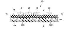
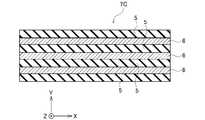
図1Aは、実施の形態に係るラベル部品7の一例を示す平面図である。また、図1Bは、図1AのI-I線に沿う断面図である。図1Aに示すように、ラベル部品7はX-Y平面に延伸している。X方向はラベル部品7の長手方向、Y方向はラベル部品7の短手方向、Z方向はX-Y平面に垂直な方向を示している。 FIG. 1A is a plan view showing an example of the
図1A及び図1Bに示すように、実施の形態に係るラベル部品7は、第1高熱伝導部材6M1と、第2高熱伝導部材6M2と、低熱伝導部材5とを備える。第1高熱伝導部材6M1は、第1領域に対応し、第1領域における発熱を拡散する。第2高熱伝導部材6M2は、第2領域に対応し、第2領域における発熱を拡散する。低熱伝導部材5の一部は、第1高熱伝導部材6M1と第2高熱伝導部材6M2との間に配置され、第1領域と第2領域との間の熱伝導を抑制する。すなわち、低熱伝導部材5の一部は、第1高熱伝導部材6M1と第2高熱伝導部材6M2との間の熱伝導を抑制する。ここで、第1領域及び第2領域は、ラベル部品7を貼り付けて放熱する対象となる半導体デバイスが配置される領域に対応する。
図1Bに示すように、低熱伝導部材5の一部は、Z方向において、第1高熱伝導部材6M1及び第2高熱伝導部材6M2それぞれと重ならないように配置されている。低熱伝導部材5の他の一部は、Z方向において、第1高熱伝導部材6M1及び第2高熱伝導部材6M2それぞれと重なるように配置されている。第1高熱伝導部材6M1及び第2高熱伝導部材6M2は、低熱伝導部材5と積層されて形成される。第1高熱伝導部材6M1及び第2高熱伝導部材6M2は、低熱伝導部材5に埋め込まれて形成されてもよい。
このように構成されたラベル部品7は、領域ごとに異なる熱伝導率を有する。第1高熱伝導部材6M1の熱伝導率及び第2高熱伝導部材6M2の熱伝導率は、共に低熱伝導部材5の熱伝導率よりも大きい。ラベル部品7は、複数の半導体デバイスが基板上に配置された構造において、それぞれ異なる領域ごとに異なる熱伝導特性を有する。
第1高熱伝導部材6M1は第1部分の一例であり、第2高熱伝導部材6M2は第2部分の一例であり、低熱伝導部材5の一部は第3部分の一例である。As shown in FIGS. 1A and 1B, the
As shown in FIG. 1B, part of the low
The
The first high heat conductive member 6M1 is an example of the first portion, the second high heat conductive member 6M2 is an example of the second portion, and a portion of the low heat
第1高熱伝導部材6M1と第2高熱伝導部材6M2は、例えば、金属層や導電性ポリマーなどで構成される。金属層としては、例えば、Cu(銅)、Al(アルミニウム)、Mo(モリブデン)、W(タングステン)等の熱伝導性又は導電性の良好な金属を主成分とする材料を適用可能である。導電性ポリマーとしては、例えば、安定性、成膜性、透明性の良好なポリチオフェン系、ポリアニリン系高分子膜を適用可能である。 The first high heat conductive member 6M1 and the second high heat conductive member 6M2 are made of, for example, a metal layer or a conductive polymer. As the metal layer, for example, a material whose main component is a metal with good thermal or electrical conductivity, such as Cu (copper), Al (aluminum), Mo (molybdenum), W (tungsten), etc., can be applied. As the conductive polymer, for example, a polythiophene-based or polyaniline-based polymer film having good stability, film-forming properties, and transparency can be applied.
一方、低熱伝導部材5は、第1高熱伝導部材6M1の熱と第2高熱伝導部材6M2の熱との間の熱伝導を抑制する絶縁材料で構成される。絶縁材料としては、例えば、テレフタル酸またはテレフタル酸ジメチルとエチレングリコールを重縮合して得られる熱可塑性ポリエステルであるポリエチレンテレフタレート(PET:polyethylene terephthalate)樹脂、アクリル系接着剤、エポキシ系の接着剤、シリコーン樹脂などで構成可能である。また、低熱伝導部材5は、上記の絶縁材料の積層構造を用いて形成されていても良い。また、上記の絶縁材料の積層構造には、文字を印刷するための層を備えていても良い。また、実施の形態に係るラベル部品7は、フレキシブルな構造を有していても良い。 On the other hand, the low heat
実施の形態に係るラベル部品7は、例えば、絶縁材料を、接着剤などで張り合わせ、または、蒸着によって形成される。
(第1の実施の形態)The
(First embodiment)
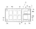
図2Aは、第1の実施の形態に係るメモリシステム1Aの平面図である。また、図2Bは、図3AのII-II線に沿う断面図である。また、図2Cは、図2AのIII-III線に沿う断面図である。 FIG. 2A is a plan view of
第1の実施の形態に係るメモリシステム1Aは、第1の基板4と、第1半導体デバイス10A、10Bと、第2半導体デバイス20と、ラベル部品7とを備える。 A
第1の基板4は、コネクタ部100と溝部15Hとを備える。溝部15Hは、X方向における第1の基板4の一端に設けられる。コネクタ部100は、溝部15HからX方向に離隔した第1の基板4の他端に設けられる。 The
第1の基板4は、例えば、プリント配線基板で構成された回路基板である。第1の基板4は、第1の面4aと、この第1の面4aに対向する第2の面4bとを有する。図2Aに示すように、第1の基板4は、X-Y平面に延伸して配置されている。X方向は、第1の基板4の長手方向、Y方向は、第1の基板4の短手方向、Z方向は、X-Y平面に垂直な方向である。以下の説明においても同様である。 The
図2Bに示すように、第1半導体デバイス10A、10Bは、第1の基板4の第1の面4a側に配置されている。 As shown in FIG. 2B, the
第1半導体デバイス10A、10Bは、例えば、NAND型フラッシュメモリである。これ以降の説明では、第1半導体デバイス10A、10Bを、NAND型フラッシュメモリ10A、10Bとも称する。NAND型フラッシュメモリ10A、10Bは、第1動作許容温度T1を有する。 The
第2半導体デバイス20は、第1の基板4の第1の面4a側に配置されている。第2半導体デバイス20は、例えば、NAND型フラッシュメモリ10A、10Bを制御するメモリコントローラである。これ以降の説明では、第2半導体デバイス20を、メモリコントローラ20とも称する。一般的に、メモリコントローラ20は、第1動作許容温度T1よりも高い第2動作許容温度T2を有する。 The
前述したように、ラベル部品7は、第1高熱伝導部材6M1と、第2高熱伝導部材6M2と、低熱伝導部材5とを有する。第1高熱伝導部材6M1は、NAND型フラッシュメモリ10A、10Bの発熱を拡散する。第2高熱伝導部材6M2は、メモリコントローラ20の発熱を拡散する。低熱伝導部材5の一部は、NAND型フラッシュメモリ10A、10Bの発熱とメモリコントローラ20の発熱との間の熱伝導を抑制する。このようにラベル部品7は、領域ごとに異なる熱伝導率を有する。 As described above, the
第1の実施の形態に係るメモリシステム1Aにおいて、ラベル部品7は、図2B及び図2Cに示すように、第1の基板4の第2の面4b側に配置されている。
図2B及び図2Cに示すように、第1高熱伝導部材6M1は、第1の基板4を挟んでNAND型フラッシュメモリ10A、10BのZ方向のマイナス方向である下方に配置されている。
第2高熱伝導部材6M2は、第1の基板4を挟んでメモリコントローラ20のZ方向のマイナス方向である下方に配置されている。In the
As shown in FIGS. 2B and 2C, the first high thermal conductivity member 6M1 is arranged below the
The second high thermal conductivity member 6M2 is arranged below the
第1の実施の形態に係るメモリシステム1Aは、領域ごとに異なる熱伝導率を持つ構造を有するラベル部品7を備える。これにより、メモリシステム1Aは、メモリコントローラ20が配置された領域では第2高熱伝導部材6M2により積極的に熱を拡散させる。また、メモリシステム1Aは、NAND型フラッシュメモリ10A、10Bが配置された領域では、低熱伝導部材5の一部により第2高熱伝導部材6M2からの受熱を抑制するとともに、第1高熱伝導部材6M1により積極的に熱を拡散させる。
(メモリシステムの搭載構造)
図3は、第1の実施の形態に係るメモリシステム1Aをホスト機器に搭載した状態の断面図である。A
(Mounting structure of memory system)
FIG. 3 is a cross-sectional view of a state in which the
メモリシステム1Aがコネクタ部100を介してホスト機器と接続された場合、メモリシステム1Aは、コネクタ部100を介してホスト機器と通信可能である。メモリシステム1Aがコネクタ部100を介してホスト機器と接続された状態で、メモリシステム1Aは、溝部15Hを介して更にホスト機器と接続可能である。ホスト装置は、コネクタ部100に接続されるコネクタ(不図示)と第2の基板8とを少なくとも備える。ホスト装置が備えるコネクタは、第2の基板8に実装される。第2の基板8は、例えば、プリント配線基板で構成された回路基板である。また、第2の基板8は、例えば、金属プレームでもよい。 When the
図3に示すように、メモリシステム1Aは、溝部15Hを介して、金属ネジ12により第2の基板8に取り付けられる。金属ネジ12は、メモリシステム1Aの第1の基板4に設けられた溝部15Hと第2の基板8に設けられたネジ切り13とを介して、第1の基板4と第2の基板8とを接続する。溝部15Hに対応するラベル部品7の一部の内壁には、第1高熱伝導部材6M1の一部が露出している。さらに、ネジ切り13の内壁には、ホスト装置の基準電位(グランド電位)となる配線の一部が露出している。
このようにして、ラベル部品7の第1高熱伝導部材6M1は、金属ネジ12を介して第2の基板8と熱的に接続される。As shown in FIG. 3, the
In this manner, the first high thermal conductivity member 6M1 of the
メモリシステム1Aは、コネクタ部100を介して、第2の基板8に実装されるコネクタと接続する。第2の基板8に実装されるコネクタが高熱伝導部材を備えている場合、このコネクタとラベル部品7とを熱的に接触させることができる。 The
第1の実施の形態に係るメモリシステム1Aは、NAND型フラッシュメモリ10A、10Bの発熱を、第1高熱伝導部材6M1及び金属ネジ12を介して第2の基板8に伝搬可能である。また、メモリコントローラ20の発熱を、第2高熱伝導部材6M2を介してコネクタ部100から外部に伝搬可能である。すなわち、NAND型フラッシュメモリ10A、10Bの発熱は、第1高熱伝導部材6M1を有するラベル部品7に伝搬する。このラベル部品7に伝搬した熱は、接する金属ネジ12を介して第2の基板8に放熱される。また、メモリコントローラ20の発生した熱は、第2の基板によって放熱される。つまり、コントローラ20の発熱は、第2高熱伝導部材6M2を有するラベル部品7に伝搬する。このラベル部品7に伝搬した熱は、ラベル部品7と接する第2の基板8、または、第2の基板8に実装されるコネクタを介して第2の基板8に熱が放熱される。第1高熱伝導部材6M1に伝搬したNAND型フラッシュメモリ10A、10Bの発熱と、第2高熱伝導部材6M2に伝搬したメモリコントローラ20の発熱との間の伝搬は、低熱伝導部材5の一部により互いに抑制される。 The
第1の実施の形態に係るメモリシステム1Aは、例えば、コンピュータの内蔵拡張カードの規格であるM.2規格に準拠している。メモリシステム1Aの第1の基板4のサイズは、M.2規格にしたがって、例えば、Y方向の幅は22mm、X方向の長さは約30mm、42mm、80mm、110mmである。この場合、ラベル部品7のサイズは、Y方向の幅は約20mm、X方向の長さは約28mm、40mm、75mm、100mmであればよい。
(第1の実施の形態の効果)The
(Effect of the first embodiment)
第1の実施の形態によれば、第1の基板4の第2の面4bに貼合されたラベル部品を有する構造により、発生する熱を適切に拡散すること又は熱の伝搬を抑制することができ、放熱性能を改善したメモリシステム1Aを提供することができる。 According to the first embodiment, the structure having the label component bonded to the
第1の実施の形態のメモリシステム1Aは、第1動作許容温度T1を有する第1半導体デバイス10A、10Bと第2動作許容温度T2を有する第2半導体デバイス20と、ラベル部品7と、を備える。異なるデバイス構造を有する第1半導体デバイス10A、10B及び第2半導体デバイス20それぞれが発生する熱は、第1高熱伝導部材6M1及び第2高熱伝導部材6M2を有するラベル部品7により、外部への放熱場所を制御することで積極的に放熱することができる。
(第2の実施の形態)A
(Second embodiment)
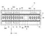
図4Aは、第2の実施の形態に係るメモリシステム1Bの平面図である。図4Bは、図4AのIV-IV線に沿う断面図である。また、図4Cは、図4AのV-V線に沿う断面図である。 FIG. 4A is a plan view of
第2の実施の形態に係るメモリシステム1Bは、第1の実施の形態と同様に、第1の基板4と、第1半導体デバイスの一例であるNAND型フラッシュメモリ10A、10Bと、第2半導体デバイスの一例であるメモリコントローラ20と、ラベル部品7とを備える。メモリシステム1Bでは、ラベル部品7は、図4B及び図4Cに示すように、第1の基板4の第1の面4a側に配置されている。
第1高熱伝導部材6M1は、図4B及び図4Cに示すように、NAND型フラッシュメモリ10A、10BのZ方向のプラス方向である上方に配置されている。
第2高熱伝導部材6M2は、メモリコントローラ20のZ方向のプラス方向である上方に配置されている。As in the first embodiment, a
As shown in FIGS. 4B and 4C, the first high thermal conductivity member 6M1 is arranged above the
The second high thermal conductivity member 6M2 is arranged above the
第2の実施の形態に係るメモリシステム1Bにおいても、領域ごとに異なる熱伝導率を持つラベル部品7を備える。これにより、メモリコントローラ20が配置された領域では第2高熱伝導部材6M2により積極的に熱を拡散させる。また、NAND型フラッシュメモリ10A、10Bが配置された領域では低熱伝導部材5の一部により第2高熱伝導部材6M2からの受熱を抑制するとともに、第1高熱伝導部材6M1により積極的に熱を拡散させる。
(メモリシステムの搭載構造)
図5は、第2の実施の形態に係るメモリシステム1Bをホスト機器に搭載した状態の断面図である。The
(Mounting structure of memory system)
FIG. 5 is a cross-sectional view of a state in which the
第2の実施の形態に係るメモリシステム1Bは、第1の実施の形態と同様に、コネクタ部100を介してホスト機器と接続され、通信可能である。また、メモリシステム1Bは、溝部15Hを介して更にホスト機器と接続可能である。ホスト装置の構成は、第1の実施の形態と同様である。 A
図5に示すように、メモリシステム1Bは、溝部15Hを介して、金属ネジ12により第2の基板8に取り付けられる。金属ネジ12は、メモリシステム1Bの第1の基板4に設けられた溝部15Hと第2の基板8に設けられたネジ切り13とを介して、第1の基板4と第2の基板8とを接続する。溝部15Hに対応するラベル部品7の一部の内壁には、第1高熱伝導部材6M1の一部が露出している。さらにネジ切り13の内壁には、ホスト装置の基準電位(グランド電位)となる配線の一部が露出している。
このようにして、ラベル部品7の第1高熱伝導部材6M1は、金属ネジ12を介して第2の基板8と熱的に接続される。As shown in FIG. 5, the
In this manner, the first high thermal conductivity member 6M1 of the
メモリシステム1Bは、コネクタ部100を介して、第2の基板8に実装されるコネクタと接続する。これにより、第2の基板8に実装されるコネクタとラベル部品7とが接し、それぞれを熱的に接続することできる。 The
第1の実施の形態に係るメモリシステム1Bは、NAND型フラッシュメモリ10A、10Bの発熱を、第1高熱伝導部材6M1及び金属ネジ12を介して第2の基板8に伝搬可能である。また、メモリコントローラ20の発熱を、第2高熱伝導部材6M2を介してその上部やコネクタ部100などから外部に放熱可能である。
(第2の実施の形態の効果)The
(Effect of Second Embodiment)
第2の実施の形態によれば、第1の基板4の第1の面4aに貼合されたラベル部品7により、発生する熱を適切に拡散することができ、放熱性能を改善したメモリシステムを提供することができる。
(第3の実施の形態)
図6Aは、第3の実施の形態に係るメモリシステム1Cの平面図である。また、図6Bは、図6AのVI-VI線に沿う断面図である。According to the second embodiment, the generated heat can be appropriately diffused by the
(Third Embodiment)
FIG. 6A is a plan view of
図6Aに示すように、第3の実施の形態に係るメモリシステム1Cは、第1の基板4と、複数の第1半導体デバイス10と、第2半導体デバイス20と、電源用のパワーマネジメント集積回路(PMIC:Power Management Integrated Circuits)24と、ダイナミックランダムアクセスメモリ(DRAM:Dynamic Random Access Memory)25と、ラベル部品7Aと、金属ネジ15A~Dを備える。
図6Bに示すように、複数の第1半導体デバイス10は、第1の基板4の第1の面4a側に配置されている。
各第1半導体デバイス10は、例えば、NAND型フラッシュメモリである。第1半導体デバイス10は、第1動作許容温度T1を有する。これ以降の説明では、第1半導体デバイス10を、NAND型フラッシュメモリ10とも称する。As shown in FIG. 6A, a
As shown in FIG. 6B , the plurality of
Each
第2半導体デバイス20は、第1の基板4の第1の面4a側に配置される。第2半導体デバイス20は、第1動作許容温度T1よりも高い第2動作許容温度T2を有する。 The
第2半導体デバイス20は、各NAND型フラッシュメモリ10を制御するメモリコントローラである。これ以降の説明では、第2半導体デバイス20を、メモリコントローラ20とも称する。
PMIC24及びDRAM25は、第1の基板4の第1の面4a側に配置されている。PMIC24は、第1半導体デバイス10及び第2半導体デバイス20に電源を供給する。DRAM25は、第2半導体デバイス20が第1半導体デバイス10を制御する際に、ワークメモリとして用いられる。The
The
ラベル部品7Aは、第1高熱伝導部材6M1と、第2高熱伝導部材6M2と、第3高熱伝導部材6M3と、低熱伝導部材5とを有する。第1高熱伝導部材6M1は、複数のNAND型フラッシュメモリ10の発熱を拡散する。第2高熱伝導部材6M2は、メモリコントローラ20の発熱を拡散する。第3高熱伝導部材6M3は、PMIC24の発熱を拡散する。低熱伝導部材5の一部は、NAND型フラッシュメモリ10の発熱とメモリコントローラ20の発熱との間の熱伝導を抑制する。また、低熱伝導部材5の一部は、NAND型フラッシュメモリ10の発熱とPMIC24の発熱との間の熱伝導を抑制する。ラベル部品7Aは、領域ごとに異なる熱伝導率を有する。 The
図6Bに示すように、ラベル部品7Aは、第1の基板4の第1の面4a側に配置されている。図6A又は6Bに示すように、第1高熱伝導部材6M1は、複数のNAND型フラッシュメモリ10のZ方向のプラス方向である上方に配置されている。第2高熱伝導部材6M2は、メモリコントローラ20のZ方向のプラス方向である上方に配置されている。第3高熱伝導部材6M3は、PMIC24のZ方向のプラス方向である上方に配置されている。 As shown in FIG. 6B, the
第3の実施の形態に係るメモリシステム1Cは、メモリシステム1A、Bと同様、領域ごとに異なる熱伝導率を持つ構造を有するラベル部品7Aを備える。これにより、メモリシステム1Cは、メモリコントローラ20が配置された領域では第2高熱伝導部材6M2により積極的に熱を拡散させる。また、メモリシステム1Cは、NAND型フラッシュメモリ10A、10Bが配置された領域では低熱伝導部材5の一部により第2高熱伝導部材6M2及び第3高熱伝導部材6M3からの受熱を抑制するとともに、第1高熱伝導部材6M1により積極的に熱を拡散させる。更に、PMIC24が配置された領域では低熱伝導部材5の一部により第1高熱伝導部材6M1及び第2高熱伝導部材6M2からの受熱を抑制するとともに、第3高熱伝導部材6M3により積極的に熱を拡散させる。
(メモリシステムの構成例)A
(Example of memory system configuration)
図6Cは、第3の実施の形態にかかるメモリシステム1Cの一例を示す斜視図である。メモリシステム1Cは、例えば、SSD(Solid State Drives)である。第3の実施の形態に係るメモリシステム1Cは、2.5インチ型のSSDの形状に関するFF(Form Factor)の規格を満足している。メモリシステム1Cは、第1ハウジング(上筐体)30Uと第2ハウジング(下筐体)30Dとで形成される筐体30を含む。
第1高熱伝導部材6M1は、図6Aに示すように、金属ネジ15A、15Bを介して筐体30に接続されている。
第2高熱伝導部材6M2は、金属ネジ15Cを介して筐体30に接続されている。
第3高熱伝導部材6M3は、金属ネジ15Dを介して筐体30に接続されている。FIG. 6C is a perspective view showing an example of a
The first high thermal conductivity member 6M1 is connected to the
The second high thermal conductivity member 6M2 is connected to the
The third high thermal conductivity member 6M3 is connected to the
メモリシステム1Cが備えるNAND型フラッシュメモリ10、メモリコントローラ20、及びPMIC24で発生した熱は、上述したラベル部品7Aによりメモリシステム1の構成部品や第1ハウジング(上筐体)30U、第2ハウジング(下筐体)30Dに熱伝搬され、そこで放熱される。 The heat generated by the
その結果、NAND型フラッシュメモリ10の温度を動作に適した温度範囲に維持して、メモリシステム1Cの良好な動作を保証することができる。なお、筐体30に収納される第1の基板4に実装されるNAND型フラッシュメモリ10、メモリコントローラ20、PMIC24、及びDRAM25のレイアウトは一例であり、必要となるメモリ容量やメモリシステム1Cのハウジングの大きさ等に応じて適宜変更可能である。また、複数の第1の基板4が筐体30に収納されてもよい。
(第3の実施の形態の効果)As a result, the temperature of the
(Effect of the third embodiment)
第3の実施の形態によれば、第1の基板4の第1の面4aに貼合されたラベル部品により、発生する熱を適切に拡散することができ、放熱性能を改善したメモリシステムを提供することができる。
(第4の実施の形態)
図7Aは、第4の実施の形態に係るメモリシステム1Dの平面図である。また、図7Bは、図7AのVII-VII線に沿う断面図である。According to the third embodiment, the generated heat can be appropriately diffused by the label component attached to the
(Fourth embodiment)
FIG. 7A is a plan view of a
第4の実施の形態に係るメモリシステム1Dは、第1の基板4と、第1半導体デバイス10と、第2半導体デバイス20と、PMIC24と、DRAM25と、ラベル部品7Aと、金属ネジ15A~Dとを備える。
図7Bに示すように、第1半導体デバイス10は、第1の基板4の第1の面4a側に配置されている。
各第1半導体デバイス10は、例えば、NAND型フラッシュメモリを備える。第1半導体デバイス10は、第1動作許容温度T1を有する。これ以降の説明では、第1半導体デバイス10を、NAND型フラッシュメモリ10とも称する。A
As shown in FIG. 7B, the
Each
第2半導体デバイス20は、第1の基板4の第1の面4a側に配置される。第2半導体デバイス20は、第1動作許容温度T1よりも高い第2動作許容温度T2を有する。
第2半導体デバイス20は、各NAND型フラッシュメモリ10を制御するメモリコントローラである。これ以降の説明では、第2半導体デバイス20を、メモリコントローラ20とも称する。
PMIC24及びDRAM25は、第1の基板4の第1の面4a側に配置されている。The
The
The
ラベル部品7Aは、第1高熱伝導部材6M1と、第2高熱伝導部材6M2と、第3高熱伝導部材6M3と、低熱伝導部材5とを有する。第1高熱伝導部材6M1は、NAND型フラッシュメモリ10からの発熱を拡散する。第2高熱伝導部材6M2は、メモリコントローラ20からの発熱を拡散する。第3高熱伝導部材6M3は、PMIC24からの発熱を拡散する。低熱伝導部材5の一部は、NAND型フラッシュメモリ10とメモリコントローラ20との間の熱伝導を抑制する。また、低熱伝導部材5の一部は、NAND型フラッシュメモリ10とPMIC24との間の熱伝導を抑制する。ラベル部品7Aは、領域ごとに異なる熱伝導率を有する。
ラベル部品7Aは、図7Bに示すように、第1の基板4の第1の面4aと対向する第2の面4b側に配置されている。
第1高熱伝導部材6M1は、図7Bに示すように、複数のNAND型フラッシュメモリ10のZ方向のマイナス方向である下方に配置されている。
第2高熱伝導部材6M2は、メモリコントローラ20のZ方向のマイナス方向である下方に配置されている。
第3高熱伝導部材6M3は、PMIC24のZ方向のマイナス方向である下方に配置されている。The
The
The first high thermal conductivity member 6M1 is arranged below the plurality of
The second high thermal conductivity member 6M2 is arranged below the
The third high thermal conductivity member 6M3 is arranged below the
第4の実施の形態に係るメモリシステム1Dは、メモリシステム1A~Cと同様、領域ごとに異なる熱伝導率を持つラベル部品7Aを備える。これにより、メモリシステム1Dは、メモリコントローラ20が配置された領域では第2高熱伝導部材6M2により積極的に熱を拡散させる。また、メモリシステム1Dは、NAND型フラッシュメモリ10A、10Bが配置された領域では低熱伝導部材5の一部により第2高熱伝導部材6M2及び第3高熱伝導部材6M3からの受熱を抑制するとともに、第1高熱伝導部材6M1により積極的に熱を拡散させる。更に、PMIC24が配置された領域では低熱伝導部材5の一部により第1高熱伝導部材6M1及び第2高熱伝導部材6M2からの受熱を抑制するとともに、第3高熱伝導部材6M3により積極的に熱を拡散させる。 A
第4の実施の形態に係るメモリシステム1Dは、図6Cと同様に、SSD装置として構成可能である。メモリシステム1Dは、第1ハウジング(上筐体)30Uと第2ハウジング(下筐体)30Dとで形成される筐体30を含む。
第1高熱伝導部材6M1は、図7Aに示すように、金属ネジ15A、15Bを介して筐体30に接続される。
第2高熱伝導部材6M2は、金属ネジ15Cを介して筐体30に接続される。
第3高熱伝導部材6M3は、金属ネジ15Dを介して筐体30に接続される。A
The first high thermal conductivity member 6M1 is connected to the
The second high thermal conductivity member 6M2 is connected to the
The third high thermal conductivity member 6M3 is connected to the
メモリシステム1Dに含まれるNAND型フラッシュメモリ10、メモリコントローラ20、及びPMIC24で発生した熱は、ラベル部品7Aによりメモリシステム1Dの構成部品や第1ハウジング(上筐体)30U、第2ハウジング(下筐体)30Dに熱伝搬され、そこで放熱される。
(第4の実施の形態の効果)The heat generated by the
(Effect of the fourth embodiment)
第4の実施の形態によれば、第1の基板4の第2の面4bに貼合されたラベル部品7Aにより、発生する熱を適切に拡散することができ、放熱性能を改善したメモリシステムを提供することができる。
(第5の実施の形態)According to the fourth embodiment, the
(Fifth embodiment)
図8Aは、第5の実施の形態に係るメモリシステム1Eの断面図である。また、図8Bは、第5の実施の形態に係るメモリシステム1Eに適用したラベル部品7Bの平面図である。また、図8Cは、第5の実施の形態に係るメモリシステム1EをSSD装置として構成した断面図である。 FIG. 8A is a cross-sectional view of
第5の実施の形態に係るメモリシステム1Eは、第1の基板4Mと、第1の基板4MのZ方向のプラス方向である上方に配置された第1の基板4Dとを備える。第1の基板4Mは例えばマザーボードと呼ばれ、第1の基板4Dはドーターボードと呼ばれることもある。 The
第1の基板4Mは、第1の面4Maと、第1の面4Maと対向する第2の面4Mbとを有する。第1の基板4Mの第1の面4Ma側には、複数のNAND型フラッシュメモリ10とメモリコントローラ20が配置される。また、第1の基板4Mの第2の面4Mb側には、複数のNAND型フラッシュメモリ10が配置されている。 The
第1の基板4Dは、第1の面4Daと、第1の面4Daと対向する第2の面4Dbとを有する。第1の基板4Dの第1の面4Da側には複数のNAND型フラッシュメモリ10が配置され、第1の基板4Dの第2の面4Db側にも複数のNAND型フラッシュメモリ10が配置されている。
第1の基板4Mと第1の基板4Dとの間には、ラベル部品7Bが配置されている。The
A
また、第1の基板4Mと第1の基板4Dとの間には、第1の基板4Mと第1の基板4Dとの間を電気的に接続するコネクタ9M、9Dが配置されている。コネクタ9Mは、第1の基板4Mの第1の面4Ma側に配置され、コネクタ9Dは、第1の基板4Dの第2の面4Db側に配置されている。第1の基板4Mに配置される複数のNAND型フラッシュメモリ10と第1の基板4Dに配置されるメモリコントローラ20との間の信号伝達及び、第1の基板4Mと第1の基板4Dとの間の電力伝達は、コネクタ9M、9Dを介して実施される。
ラベル部品7Bは、第1高熱伝導部材6M1と、第2高熱伝導部材6M2と、低熱伝導部材5とを有する。ラベル部品7Bは、図8Bに示すように、空洞部19を有する。第1の基板4Mと第1の基板4Dとの間にラベル部品7Bが配置された状態では、空洞部19に、コネクタ9M、9Dが配置される。第1高熱伝導部材6M1は、NAND型フラッシュメモリ10の発熱を拡散する。第2高熱伝導部材6M2は、メモリコントローラ20の発熱を拡散する。 The
第1高熱伝導部材6M1は、図8Aに示すように、第1の基板4Mの第1の面4Ma側に配置されたNAND型フラッシュメモリ10のZ方向のプラス方向である上方に配置されている。また、第1高熱伝導部材6M1は、図8Aに示すように、第1の基板4Dの第2の面4Dbが側に配置されたNAND型フラッシュメモリ10のZ方向のマイナス方向である下方に配置されている。 As shown in FIG. 8A, the first high thermal conductivity member 6M1 is arranged above the
第2高熱伝導部材6M2は、図8Aに示すように、第1の基板4Mの第1の面4Ma側に配置されたメモリコントローラ20のZ方向のプラス方向である上方に配置されている。また、第2高熱伝導部材6M2は、図8Aに示すように、第1の基板4Dの第1の面4Da側に配置されたNAND型フラッシュメモリ10のZ方向のマイナス方向である下方に配置されている。
(メモリシステムの構成例)As shown in FIG. 8A, the second high thermal conductivity member 6M2 is arranged above the
(Example of memory system configuration)
図8Cに示すように、メモリシステム1Eは、第1ハウジング(上筐体)30Uと第2ハウジング(下筐体)30Dとで形成される筐体30を含む。
第1高熱伝導部材6M1の一部は、第1ハウジング(上筐体)30Uと接している。また、第2高熱伝導部材6M2の一部は、第1ハウジング(上筐体)30Uと接している。As shown in FIG. 8C, the
A portion of the first high thermal conductivity member 6M1 is in contact with the first housing (upper housing) 30U. A portion of the second high thermal conductivity member 6M2 is in contact with the first housing (upper housing) 30U.
メモリシステム1Eが備えるNAND型フラッシュメモリ10、メモリコントローラ20で発生した熱は、上述したラベル部品7Bによりメモリシステム1Eの構成部品や第1ハウジング(上筐体)30U、第2ハウジング(下筐体)30Dに伝搬され、そこで放熱される。 The heat generated by the
その結果、NAND型フラッシュメモリ10の温度を動作に適した温度範囲に維持して、メモリシステム1Eの良好な動作を保証することができる。
(第5の実施の形態の効果)As a result, the temperature of the
(Effect of the fifth embodiment)
第5の実施の形態によれば、複数の第1の基板(4D、4M)の間に貼合されたラベル部品7Bにより、発生する熱を適切に拡散することができ、放熱性能を改善したメモリシステムを提供することができる。
(ラベル部品の変形例)
(変形例1)
図9は、実施の形態の変形例1に係るラベル部品7Cの平面図である。According to the fifth embodiment, the generated heat can be appropriately diffused by the
(Modified example of label part)
(Modification 1)
FIG. 9 is a plan view of a
実施の形態の変形例1に係るラベル部品7Cは、図9に示すように、複数の高熱伝導部材6と複数の低熱伝導部材5とを備える。複数の高熱伝導部材6は、X方向に延びている。また、複数の低熱伝導部材5もX方向に延びている。複数の高熱伝導部材6と複数の低熱伝導部材5は、図9に示すように、Y方向において交互に配置されている。このため、実施の形態の変形例1に係るラベル部品7Cは、X方向に熱伝導性が高く、Y方向に熱伝導性が低い。
(変形例1の効果)A
(Effect of Modification 1)
実施の形態の変形例1に係るラベル部品7Cでは、複数の高熱伝導部材と複数の低熱伝導部材を互い違いに平行に配置することによって、X方向に熱伝導性が高く、X方向に垂直なY方向には熱伝導性が低い特性を持たせることができ、熱伝導の方向性を制御することができる。
(変形例2)In the
(Modification 2)
高熱伝導部材6は、一層である必要はなく、多層化しても良い。また全層で同一形状である必要はない。高熱伝導部材6を多層構造として、各層の高熱伝導部材6の大きさ(又は範囲又は面積)を異ならせる構成を採用しても良い。
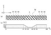
図10(a)は、実施の形態の変形例2に係るラベル部品7Dの断面図である。The high
FIG. 10(a) is a cross-sectional view of a
実施の形態の変形例2に係るラベル部品7Dは、図10(a)に示すように、複数の高熱伝導部材61、62、63と低熱伝導部材5とを備える。複数の高熱伝導部材61、62、63は、図10(a)に示すように、低熱伝導部材5をZ方向に挟んで、積層化されている。また、高熱伝導部材61のZ方向のプラス方向及び高熱伝導部材63のZ方向のマイナス方向にも低熱伝導部材5が配置されている。 A
複数の高熱伝導部材61、62、63は、X方向(又はY方向)に延びている。複数の高熱伝導部材61、62、63は、例えば、図10(a)に示すように、X方向に延びる長さが異なっている。
図10(b)は、図10(a)に対応したX方向の位置毎のZ方向における熱伝導率TCの分布の様子を表した模式図である。A plurality of high
FIG. 10(b) is a schematic diagram showing the distribution of the thermal conductivity TC in the Z direction for each position in the X direction corresponding to FIG. 10(a).
実施の形態の変形例2に係るラベル部品7Dでは、図10(b)に示すように、3層の高熱伝導部材61、62、63が存在する範囲X=0~X1、X6~XMでは、熱伝導率TC=TC1である。2層の高熱伝導部材61、62が存在する範囲X=X1~X2、X5~X6では、熱伝導率TCは、TC1よりも低下している。X=X2及びX5では、TC=TC2である。1層の高熱伝導部材61が存在する範囲X=X2~X3、X4~X5では、熱伝率TCは、更に低下している。高熱伝導部材が存在しない範囲X=X3~X4では、熱伝導率TC=TC0である。TC0の値は、TC2よりも更にも小さい。
(変形例2の効果)In the
(Effect of modification 2)
実施の形態の変形例2に係るラベル部品7Dでは、互いに積層される複数の高熱伝導部材のある方向の長さ、大きさ、面積、又は範囲を調整することによって、熱伝導率TCの分布を調整することができる。
(変形例3)
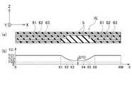
図11(a)は、実施の形態の変形例3に係るラベル部品7Eの断面図である。In the
(Modification 3)
FIG. 11(a) is a cross-sectional view of a
実施の形態の変形例3に係るラベル部品7Eは、図11(a)に示すように、複数の高熱伝導部材61、62、63と低熱伝導部材5とを備える。複数の高熱伝導部材61、62、63は、図11(a)に示すように、低熱伝導部材5をZ方向に挟んで、積層化されている。また、高熱伝導部材61のZ方向のプラス方向及び高熱伝導部材63のZ方向のマイナス方向にも低熱伝導部材5が配置されている。 A
また、複数の高熱伝導部材61、62、63は、X方向(又はY方向)に延びている。複数の高熱伝導部材61、62、63は、例えば、図11(a)に示すように、X方向に延びる長さが異なっている。変形例2と異なるのは、高熱伝導部材61がX=0~XMまでX方向に連続して延びている点である。その他の構成は、変形例2と同様である。
図11(b)は、図11(a)に対応したX方向の位置毎のZ方向における熱伝導率TCの分布の様子を表した模式図である。Also, the plurality of high
FIG. 11(b) is a schematic diagram showing the distribution of thermal conductivity TC in the Z direction for each position in the X direction corresponding to FIG. 11(a).
実施の形態の変形例3に係るラベル部品7Eでは、図11(b)に示すように、3層の高熱伝導部材61、62、63が存在する範囲X=0~X1、X6~XMでは、熱伝導率TC=TC1である。2層の高熱伝導部材61、62が存在する範囲X=X1~X2、X5~X6では、熱伝導率TCはTC1よりも低下している。X=X2及びX=X5では、TC=TC2である。1層の高熱伝導部材61が存在する範囲X=X3~X4では、熱伝率TCは、更に低下している。図11(b)において、破線で示される熱伝導率TCは、変形例2における熱伝導率TCの分布に対応しており、実線で示される熱伝導率TCは、変形例3における熱伝導率TCの分布に対応している。1層の高熱伝導部材61が存在する範囲X=X3~X4では、変形例3の熱伝率TCは、変形例2に比べてΔTC上昇している。
(変形例3の効果)In the
(Effect of modification 3)
実施の形態の変形例3に係るラベル部品7Eでは、互いに積層される複数の高熱伝導部材のある方向の長さ、大きさ、面積、又は範囲を調整することによって、熱伝導率TCの分布を調整することができる。
(メモリシステムの構成)
次に、実施の形態に係るメモリシステムのブロックの構成を説明する。In the
(Configuration of memory system)
Next, the block configuration of the memory system according to the embodiment will be described.
図12は、実施の形態に係るメモリシステム1のブロック図である。実施の形態に係るメモリシステム1は、SSDとして構成される。図12に示すように、メモリシステム1は、複数のNAND型フラッシュメモリ10と、DRAM25と、メモリコントローラ20と、PMIC24とを備える。メモリシステム1は、ホスト装置2と接続可能である。 FIG. 12 is a block diagram of
NAND型フラッシュメモリ10は、データを不揮発に記憶可能な不揮発性メモリであり、それぞれ独立して動作することができる。尚、NAND型フラッシュメモリ10の個数は特に限定されず、任意の個数に設計することができる。NAND型フラッシュメモリ10とメモリコントローラ20は、複数のチャネルを介して接続される。NAND型フラッシュメモリ以外の不揮発性メモリとしては、NOR型フラッシュメモリ、抵抗変化メモリ(ReRAM:Resistive Random Access Memory)、相変化メモリ(PCM: Phase-Change Memory)、強誘電体メモリ(FeRAM:Ferroelectric Random Access Memory)、磁気トンネル接合(MTJ:Magneto Tunnel Junction)抵抗変化素子が適用可能である。 The
DRAM25は、データを一時的に記憶可能な揮発性メモリである。尚、メモリシステム1が備える揮発性メモリの個数は任意の個数に設計することができる。また、揮発性メモリは、DRAMに限定されない。例えば揮発性メモリとしてSRAM(Static Random Access Memory)等を用いても良い。 The
メモリコントローラ20は、NAND型フラッシュメモリ10及びDRAM25に各種動作を命令することができる。また、メモリコントローラ20は、外部のホスト機器2からの命令に基づいた動作と、ホスト機器2からの命令に依らない動作とを実行することができる。 The
PMIC24は、電源ライン52を介してメモリコントローラ20に必要な電源を供給する。PMIC24は、電源ライン50を介してNAND型フラッシュメモリ10及びDRAM25に必要な電源を供給する。PMIC24は、例えば、DC-DCコンバータ、LDO(Low Drop Output)レギュレータ、スイッチングレギュレータ等を備えている。 The
図12に示すようにメモリコントローラ20は、例えば、CPU(Central Processing Unit)21と、内蔵メモリ(RAM:Random Access Memory)22と、ホストI/F回路23と、NANDI/F回路26と、DRAMI/F回路27とを備えている。メモリコントローラ20の構成はあくまで一例であり、これに限定されない。 As shown in FIG. 12, the
CPU21は、メモリコントローラ20全体の動作を制御する。例えばCPU21は、ホスト機器2から受信した読み出し命令に応答して読み出しコマンドを発行して、発行したコマンドをNANDI/F回路26に送信する。 The
内蔵メモリ22は、CPU21の作業領域として使用される記憶領域である。例えば、内蔵メモリ22には、NAND型フラッシュメモリ10を管理するためのパラメータや、各種の管理テーブル等が展開される。例えば、内蔵メモリ22は、ホスト機器2から受信した命令の待ち行列(コマンドキュー)を保持する。また、内蔵メモリ22は、ホスト機器2から書き込みを要求されたデータに関連付けられた論理アドレスをNAND型フラッシュメモリ10の物理ブロックアドレス(PBA:Physical Block Address)に変換するためのアドレス変換テーブルを保持する。このアドレス変換テーブルは、例えばNAND型フラッシュメモリ10に格納され、メモリシステム1の起動時に読み出されて内蔵メモリ22に展開される。内蔵メモリ22としては、例えばSRAM等の揮発性メモリが用いられる。 The built-in
ホストI/F回路23は、ホスト機器2に接続され、メモリシステム1とホスト機器2との間の通信を司る。例えばホストI/F回路23は、メモリシステム1とホスト機器2との間で、データ、コマンド、及びアドレスの転送を制御する。ホストI/F回路23は、例えばSATA、SAS、PCIe(登録商標)等の通信I/F規格をサポートする。つまり、メモリシステム1に接続されるホスト機器2としては、例えばSATA、SAS、PCIe等のI/Fを含むコンピュータ等が挙げられる。 The host I/
NANDI/F回路26は、NAND型フラッシュメモリ10に接続され、メモリコントローラ20とNAND型フラッシュメモリ10との間の通信を司る。NANDI/F回路26は、NANDI/F規格に基づいて構成されている。 The NAND I/
DRAMI/F回路27は、DRAM25に接続され、メモリコントローラ20とDRAM25との間の通信を司る。DRAMI/F回路27は、DRAMI/F規格に基づいて構成されている。尚、DRAMI/F回路27の構成はこれに限定されず、揮発性メモリの種類に基づいて変更することができる。
(電子機器)A DRAM I/
(Electronics)
図13は、実施の形態にかかる電子機器2の一例を示す斜視図である。電子機器2は、ホスト機器2での一例であり、例えば、パーソナルコンピュータである。実施の形態にかかるメモリシステム1は、例えばキーボード32の手前側のパームレスト34の下の内部空間に収納される。メモリシステム1の第1の基板4上には、例えばNAND型フラッシュメモリ10A、10Bとメモリコントローラ20が実装されている。 FIG. 13 is a perspective view showing an example of the
実施の形態にかかる電子機器2は、ホスト機器2とインタフェース接続されるメモリシステム1を備える。メモリシステム1は、第1の基板4と、第1半導体デバイスの一例である第1電子部品10A、10Bと、第2半導体デバイスの一例である第2電子部品20と、ラベル部品7とを備える。第1電子部品10A、10Bは、第1の基板4の第1の面側に配置され、第1動作許容温度を有する。第2電子部品は、第1の基板4の第1の面側に配置され、第1動作許容温度よりも高い第2動作許容温度を有する。ラベル部品7は、第1電子部品からの発熱を拡散する第1部分の一例である第1高熱伝導部材と、第2電子部品20からの発熱を拡散する第2部分の一例である第2高熱伝導部材と、第1電子部品10A、10Bと第2電子部品20との間の熱伝導を抑制する第3部分の一例である低熱伝導部材とを備え、第1の基板4に貼合されている。 An
メモリシステム1に含まれるメモリコントローラ20で発生した熱は、上述したラベル部品7により電子機器2の構成部品を介して放熱し、電子機器2側に内蔵されたファンによる気流により、電子機器2の排気口(図示せず)から排気と共に排出する。その結果、NAND型フラッシュメモリ10A、10Bの温度を動作に適した温度範囲に維持して、電子機器2の良好な動作を保証することができる。 The heat generated by the
なお、電子機器2に収納されるメモリシステム1の第1の基板4に実装されるNAND型フラッシュメモリ10A、10Bとメモリコントローラ20のレイアウトは一例である。このレイアウトは、メモリシステム1に要求されるメモリ容量や電子機器2におけるメモリシステム1の搭載スペースの大きさ等に応じて適宜変更可能である。また、複数のメモリシステム1が電子機器2に収納されてもよい。また、電子機器2に収納されるメモリシステム1には、上述の第1~第5の実施の形態に係るメモリシステム1、1A、1B、1C、1D、1Eの何れかを適用しても良い。また、ラベル部品としても実施の形態に係るラベル部品7(図1A及び図1B)、実施の形態の変形例に係るラベル部品7A、7B、7C、7D、7E(図6~7、図8、図9、図10、図11)を用いても良い。 The layout of the
本発明のいくつかの実施の形態を説明したが、これらの実施の形態は、例として提示したものであり、発明の範囲を限定することは意図していない。これら新規な実施の形態は、その他の様々な形態で実施されることが可能であり、発明の要旨を逸脱しない範囲で、種々の省略、置き換え、変更を行うことができる。これら実施の形態やその変形は、発明の範囲や要旨に含まれるとともに、特許請求の範囲に記載された発明とその均等の範囲に含まれる。 While several embodiments of the invention have been described, these embodiments have been presented by way of example and are not intended to limit the scope of the invention. These novel embodiments can be implemented in various other forms, and various omissions, replacements, and modifications can be made without departing from the scope of the invention. These embodiments and their modifications are included in the scope and gist of the invention, and are included in the scope of the invention described in the claims and equivalents thereof.
1、1A、1B、1C、1D、1E…メモリシステム
2…ホスト機器(電子機器)
4、4M、4D…第1の基板
4a、4Ma、4Da…第1の面
4b、4Mb、4Db…第2の面
5、5D、5U1、5U2…低熱伝導部材
6、6M1、6M2、6M3、61、62、63…高熱伝導部材
7、7A、7B、7C、7D、7E…ラベル部品
8…第2の基板
9D、9M…コネクタ
100…コネクタ部
10、10A、10B…NAND型フラッシュメモリ
12、15A~15D…金属ネジ
13…ネジ切り
15H…溝部
19…空洞部
20…メモリコントローラ
21…CPU
22…内蔵メモリ(RAM)
23…ホストI/F回路
24…パワーマネジメント集積回路(PMIC)
25…ダイナミックランダムアクセスメモリ(DRAM)
26…NANDI/F回路
27…DRAMI/F回路
30…筐体
30U…上筐体
30D…下筐体
32…キーボード
34…パームレスト
50、52…電源ライン1, 1A, 1B, 1C, 1D, 1E...
4, 4M, 4D...
22... Built-in memory (RAM)
23 Host I/
25 Dynamic random access memory (DRAM)
26 NANDI/
Claims (9)
Translated fromJapanese前記第1の基板の前記第1の面に配置される第1半導体デバイスと、
前記第1の基板の前記第1の面に配置される第2半導体デバイスと、
前記第1半導体デバイスからの発熱を拡散する第1部分と、前記第2半導体デバイスからの発熱を拡散する第2部分と、前記第1部分と前記第2部分との間に配置され、前記第1部分の熱と前記第2部分の熱との間の熱伝導を抑制する第3部分とを有するラベル部品と、
を備え、
前記第1部分の第1熱伝導率及び前記第2部分の第2熱伝導率はともに、前記第3部分の第3熱伝導率よりも高い、メモリシステム。a first substrate having a first surface;
a first semiconductor device disposed on the first side of the first substrate;
a second semiconductor device disposed on the first side of the first substrate;
a first portion for diffusing heat generated from the first semiconductor device; a second portion for diffusing heat generated from the second semiconductor device; a label component having a third portion that inhibits heat transfer between heat in one portion and heat in the second portion;
with
The memory system, wherein the first thermal conductivity of the first portion and the second thermal conductivity of the second portion are both higher than the third thermal conductivity of the third portion.
前記第1部分は、前記第1半導体デバイスが配置される位置に対応した位置に配置され、
前記第2部分は、前記第2半導体デバイスが配置される位置に対応した位置に配置される、請求項1に記載のメモリシステム。The label component is arranged on the first surface side of the first substrate,
the first portion is arranged at a position corresponding to a position where the first semiconductor device is arranged;
2. The memory system according to claim 1, wherein said second portion is arranged at a position corresponding to a position where said second semiconductor device is arranged.
前記ラベル部品は、前記第2の面側に配置され、
前記第1部分は、前記第1半導体デバイスが配置される位置に対応した位置に配置され、
前記第2部分は、前記第2半導体デバイスが配置される位置に対応した位置に配置される、請求項1に記載のメモリシステム。The first substrate further has a second surface facing the first surface,
The label component is arranged on the second surface side,
the first portion is arranged at a position corresponding to a position where the first semiconductor device is arranged;
2. The memory system according to claim 1, wherein said second portion is arranged at a position corresponding to a position where said second semiconductor device is arranged.
前記筐体に接続される金属ネジと、を更に備え、
前記第1部分は、前記筐体に前記金属ネジを介して接続される、請求項1~3の何れか1項に記載のメモリシステム。a housing;
and a metal screw connected to the housing,
4. The memory system according to claim 1, wherein said first portion is connected to said housing via said metal screw.
前記第1の基板と前記第2の基板とを接続するコネクタと、
を備える、請求項1~4の何れか1項に記載のメモリシステム。a second substrate facing the first substrate with the label component therebetween;
a connector that connects the first substrate and the second substrate;
The memory system according to any one of claims 1 to 4, comprising:
前記メモリシステムは、
前記第1の基板と異なる第2の基板と、
前記第1の基板と前記第2の基板とを前記溝部を介して接続する金属ネジと、
を更に備え、
前記第1部分は、前記金属ネジを介して前記第2の基板と接続される、請求項1~3のいずれか1項に記載のメモリシステム。The first substrate further has a first end and a groove formed in the first end,
The memory system is
a second substrate different from the first substrate;
a metal screw that connects the first substrate and the second substrate through the groove;
further comprising
4. The memory system according to claim 1, wherein said first portion is connected to said second substrate via said metal screw.
前記第2部分は、前記コネクタに近接して配置される、請求項6に記載のメモリシステム。the first substrate further has a second end different from the first end and a connector disposed at the second end;
7. The memory system of claim 6, wherein said second portion is positioned proximate to said connector.
前記基板において前記第1半導体デバイスが配置される位置に対応した位置に配置される第1部分と、
前記基板において前記第2半導体デバイスが配置される位置に対応した位置に配置される第2部分と、
前記第1部分と前記第2部分との間に配置され、前記第1部分の熱と前記第2部分の熱との間の熱伝導を抑制する第3部分と、
を備え、
前記第1部分の第1熱伝導率及び前記第2部分の第2熱伝導率はともに、前記第3部分の第3熱伝導率よりも高い、ラベル部品。A label component attached to a substrate comprising a first semiconductor device and a second semiconductor device,
a first portion arranged on the substrate at a position corresponding to a position where the first semiconductor device is arranged;
a second portion arranged on the substrate at a position corresponding to a position where the second semiconductor device is arranged;
a third portion disposed between the first portion and the second portion for suppressing heat conduction between the heat of the first portion and the heat of the second portion;
with
A label component, wherein both the first thermal conductivity of the first portion and the second thermal conductivity of the second portion are higher than the third thermal conductivity of the third portion.
Priority Applications (6)
| Application Number | Priority Date | Filing Date | Title |
|---|---|---|---|
| JP2021048945AJP2022147620A (en) | 2021-03-23 | 2021-03-23 | Memory system and label component |
| TW111133125ATWI836585B (en) | 2021-03-23 | 2021-06-17 | memory system |
| TW110122030ATWI779669B (en) | 2021-03-23 | 2021-06-17 | Memory system and label parts |
| CN202110905760.7ACN115116493A (en) | 2021-03-23 | 2021-08-06 | Storage system and tag component |
| US17/463,447US11672102B2 (en) | 2021-03-23 | 2021-08-31 | Memory system and label component |
| US18/306,891US12058843B2 (en) | 2021-03-23 | 2023-04-25 | Memory system and label component |
Applications Claiming Priority (1)
| Application Number | Priority Date | Filing Date | Title |
|---|---|---|---|
| JP2021048945AJP2022147620A (en) | 2021-03-23 | 2021-03-23 | Memory system and label component |
Publications (1)
| Publication Number | Publication Date |
|---|---|
| JP2022147620Atrue JP2022147620A (en) | 2022-10-06 |
Family
ID=83324575
Family Applications (1)
| Application Number | Title | Priority Date | Filing Date |
|---|---|---|---|
| JP2021048945APendingJP2022147620A (en) | 2021-03-23 | 2021-03-23 | Memory system and label component |
Country Status (4)
| Country | Link |
|---|---|
| US (2) | US11672102B2 (en) |
| JP (1) | JP2022147620A (en) |
| CN (1) | CN115116493A (en) |
| TW (2) | TWI779669B (en) |
Families Citing this family (6)
| Publication number | Priority date | Publication date | Assignee | Title |
|---|---|---|---|---|
| JP2022147620A (en) | 2021-03-23 | 2022-10-06 | キオクシア株式会社 | Memory system and label component |
| JP2023111629A (en)* | 2022-01-31 | 2023-08-10 | パナソニックIpマネジメント株式会社 | electrical equipment |
| US12158785B2 (en)* | 2022-02-10 | 2024-12-03 | Micron Technology, Inc. | Thermal islanding heatsink |
| US20230384842A1 (en)* | 2022-05-26 | 2023-11-30 | Intel Corporation | Socketed memory architecture package and method |
| WO2025014741A1 (en)* | 2023-07-12 | 2025-01-16 | Micron Technology, Inc. | Thermal islanding systems |
| US12282611B2 (en)* | 2023-08-15 | 2025-04-22 | Dell Products L.P. | Information handling system hybrid heat block keyboard |
Family Cites Families (37)
| Publication number | Priority date | Publication date | Assignee | Title |
|---|---|---|---|---|
| US6452804B1 (en)* | 1999-07-15 | 2002-09-17 | Incep Technologies, Inc. | Method and apparatus for thermal and mechanical management of a power regulator module and microprocessor in contact with a thermally conducting plate |
| US7301776B1 (en)* | 2004-11-16 | 2007-11-27 | Super Talent Electronics, Inc. | Light-weight flash hard drive with plastic frame |
| US6762939B2 (en)* | 2002-02-20 | 2004-07-13 | Intel Corporation | Thermal solution for a mezzanine card |
| US7566001B2 (en)* | 2003-08-29 | 2009-07-28 | Semiconductor Energy Laboratory Co., Ltd. | IC card |
| TWI440207B (en)* | 2005-07-27 | 2014-06-01 | Showa Denko Kk | The light emitting diode element is equipped with a light source |
| JP4155999B2 (en)* | 2006-06-02 | 2008-09-24 | 株式会社ソニー・コンピュータエンタテインメント | Semiconductor device and manufacturing method of semiconductor device |
| JP2007332293A (en) | 2006-06-16 | 2007-12-27 | Panac Co Ltd | Adhesive label |
| CN101505029B (en)* | 2008-02-04 | 2011-11-30 | 北京中视中科光电技术有限公司 | Laser and heat radiation device |
| JP2011023587A (en)* | 2009-07-16 | 2011-02-03 | Shinko Electric Ind Co Ltd | Semiconductor device |
| JP4806079B2 (en)* | 2010-02-17 | 2011-11-02 | 株式会社東芝 | Storage device |
| JP2011170566A (en)* | 2010-02-17 | 2011-09-01 | Toshiba Corp | Semiconductor storage device and electronic device |
| JP2013033914A (en)* | 2011-06-27 | 2013-02-14 | Toshiba Corp | Semiconductor device |
| US9437518B2 (en)* | 2012-10-29 | 2016-09-06 | Samsung Electronics Co., Ltd. | Semiconductor module |
| KR102046985B1 (en)* | 2012-11-26 | 2019-12-03 | 삼성전자 주식회사 | secondary memory device |
| US9123686B2 (en)* | 2013-04-12 | 2015-09-01 | Western Digital Technologies, Inc. | Thermal management for solid-state drive |
| JP2016071269A (en)* | 2014-09-30 | 2016-05-09 | 株式会社東芝 | Electronic apparatus and system |
| US9609739B2 (en)* | 2015-03-10 | 2017-03-28 | Kabushiki Kaisha Toshiba | Electronic device |
| US9831150B2 (en)* | 2015-03-11 | 2017-11-28 | Toshiba Memory Corporation | Semiconductor device and electronic device |
| JP2016170712A (en)* | 2015-03-13 | 2016-09-23 | 株式会社東芝 | Server system and storage device |
| JP2016192444A (en)* | 2015-03-30 | 2016-11-10 | 株式会社東芝 | Semiconductor device |
| US9823691B2 (en)* | 2015-07-23 | 2017-11-21 | Toshiba Memory Corporation | Semiconductor storage device |
| KR102361637B1 (en)* | 2015-08-25 | 2022-02-10 | 삼성전자주식회사 | Solid state drive apparatus |
| EP3479662B1 (en)* | 2016-06-29 | 2023-03-01 | At&S Austria Technologie & Systemtechnik Aktiengesellschaft | Cooling component carrier material by carbon structure within dielectric shell |
| JP2018018853A (en)* | 2016-07-25 | 2018-02-01 | レノボ・シンガポール・プライベート・リミテッド | Electronic device and electronic apparatus |
| JP2018157005A (en)* | 2017-03-16 | 2018-10-04 | 東芝メモリ株式会社 | Electronics |
| TWM561980U (en)* | 2017-12-05 | 2018-06-11 | 技嘉科技股份有限公司 | Main circuit board with heat dissipation holes and electronic device thereof |
| JP7037977B2 (en) | 2018-03-26 | 2022-03-17 | サトーホールディングス株式会社 | Label affixing device, label affixing method |
| KR20200138302A (en)* | 2018-03-28 | 2020-12-09 | 미쓰비시 마테리알 가부시키가이샤 | Insulated circuit board with heat sink attached |
| US11387224B2 (en)* | 2018-10-11 | 2022-07-12 | Intel Corporation | Phase change material in substrate cavity |
| TWI685422B (en)* | 2019-01-29 | 2020-02-21 | 兆科科技有限公司 | Heat dissipation label with high contrast color difference forming identification mark |
| US11317540B2 (en)* | 2019-09-20 | 2022-04-26 | Samsung Electronics Co., Ltd. | Solid state drive apparatus and data storage apparatus including the same |
| CN211044827U (en)* | 2019-10-16 | 2020-07-17 | 惠州昌钲新材料有限公司 | Radiating and labeling of NVME interface SSD card |
| US20210272885A1 (en)* | 2020-02-27 | 2021-09-02 | Intel Corporation | Interposer heat spreader |
| JP2021150074A (en)* | 2020-03-17 | 2021-09-27 | キオクシア株式会社 | Electronic apparatus and stacking connector |
| JP2021170570A (en)* | 2020-04-14 | 2021-10-28 | キオクシア株式会社 | Semiconductor storage device |
| JP2022047385A (en)* | 2020-09-11 | 2022-03-24 | キオクシア株式会社 | Printed wiring board and memory system |
| JP2022147620A (en) | 2021-03-23 | 2022-10-06 | キオクシア株式会社 | Memory system and label component |
- 2021
- 2021-03-23JPJP2021048945Apatent/JP2022147620A/enactivePending
- 2021-06-17TWTW110122030Apatent/TWI779669B/enactive
- 2021-06-17TWTW111133125Apatent/TWI836585B/enactive
- 2021-08-06CNCN202110905760.7Apatent/CN115116493A/enactivePending
- 2021-08-31USUS17/463,447patent/US11672102B2/enactiveActive
- 2023
- 2023-04-25USUS18/306,891patent/US12058843B2/enactiveActive
Also Published As
| Publication number | Publication date |
|---|---|
| US11672102B2 (en) | 2023-06-06 |
| US20220312627A1 (en) | 2022-09-29 |
| US20230269914A1 (en) | 2023-08-24 |
| US12058843B2 (en) | 2024-08-06 |
| TW202238316A (en) | 2022-10-01 |
| CN115116493A (en) | 2022-09-27 |
| TW202307612A (en) | 2023-02-16 |
| TWI779669B (en) | 2022-10-01 |
| TWI836585B (en) | 2024-03-21 |
Similar Documents
| Publication | Publication Date | Title |
|---|---|---|
| JP2022147620A (en) | Memory system and label component | |
| US10551885B2 (en) | Solid state drive apparatus | |
| AU2019202222B2 (en) | Thermal management for solid-state drive | |
| KR102767456B1 (en) | Solid state drive device and computer server system having the same | |
| US10955882B2 (en) | Solid-state drive case and solid-state drive device using the same | |
| US11310905B2 (en) | Memory device including a conductive plate with a shielding region | |
| US11744046B2 (en) | Semiconductor storage device | |
| CN105874890A (en) | Heat Dissipation of Substrate Assembly | |
| US11887911B2 (en) | Semiconductor storage device | |
| US9377828B2 (en) | Adjustable heat sink supporting multiple platforms and system configurations | |
| JP2016071269A (en) | Electronic apparatus and system | |
| TWM613246U (en) | Ssd and ssd system | |
| US10446194B2 (en) | Memory module including battery | |
| US11317542B2 (en) | Technologies for improving processor thermal design power | |
| JP2022111617A (en) | memory system | |
| CN215600090U (en) | SSD and SSD system | |
| TWI824597B (en) | Data storage device with double-layer circuit board | |
| US20250024593A1 (en) | Apparatus and systems to retain a printed circuit board between mounting plates | |
| JP7653588B2 (en) | Storage Unit | |
| CN117377200A (en) | Data storage device with double-layer circuit board | |
| CN112397107A (en) | Heating and radiating structure of storage device |