JP2022144044A - IC card, portable electronic device and IC card processing device - Google Patents
IC card, portable electronic device and IC card processing deviceDownload PDFInfo
- Publication number
- JP2022144044A JP2022144044AJP2021044884AJP2021044884AJP2022144044AJP 2022144044 AJP2022144044 AJP 2022144044AJP 2021044884 AJP2021044884 AJP 2021044884AJP 2021044884 AJP2021044884 AJP 2021044884AJP 2022144044 AJP2022144044 AJP 2022144044A
- Authority
- JP
- Japan
- Prior art keywords
- card
- antenna
- capacity
- processor
- capacitor
- Prior art date
- Legal status (The legal status is an assumption and is not a legal conclusion. Google has not performed a legal analysis and makes no representation as to the accuracy of the status listed.)
- Pending
Links
Images

Landscapes
- Variable-Direction Aerials And Aerial Arrays (AREA)
- Support Of Aerials (AREA)
Abstract
Description
Translated fromJapanese本発明の実施形態は、ICカード、携帯可能電子装置及びICカード処理装置に関する。 Embodiments of the present invention relate to IC cards, portable electronic devices, and IC card processing devices.
非接触で上位装置とデータを送受信するICカードが提供されている。そのようなICカードは、所定の周波数の電波で通信する。そのため、ICカードは、アンテナのインダクタンスに応じたコンデンサ容量を有するチップを備える。 An IC card is provided that transmits and receives data to and from a higher-level device in a non-contact manner. Such IC cards communicate using radio waves of a predetermined frequency. Therefore, the IC card has a chip having a capacitor capacity corresponding to the inductance of the antenna.
ICカードのアンテナは、ICカードの種類によって異なる。その結果、従来、ベンダーは、各種のアンテナに対応するチップを製造する必要がある。 The IC card antenna differs depending on the type of IC card. As a result, conventionally, vendors have to manufacture chips for each type of antenna.
上記の課題を解決するため、複数種類のアンテナに対応することができるICカード、携帯可能電子装置及びICカード処理装置を提供する。 In order to solve the above problems, an IC card, a portable electronic device, and an IC card processing device are provided that are compatible with multiple types of antennas.
実施形態によれば、ICカードは、通信部と、アンテナと、コンデンサと、変更機構と、プロセッサと、を備える。通信部は、外部装置とデータを送受信する。 According to embodiments, an IC card comprises a communication unit, an antenna, a capacitor, a change mechanism, and a processor. The communication unit transmits and receives data to and from an external device.
アンテナは、非接触で通信する。コンデンサは、前記アンテナに接続する。変更機構は、前記コンデンサの容量を変更する。プロセッサは、前記通信部を通じて、前記容量を変更させる変更コマンドを前記外部装置から受信し、前記変更機構を用いて、前記変更コマンドに従って前記容量を変更する。 The antenna communicates contactlessly. A capacitor connects to the antenna. A change mechanism changes the capacity of the capacitor. The processor receives a change command for changing the capacity from the external device through the communication unit, and changes the capacity according to the change command using the change mechanism.
以下、実施形態について、図面を参照して説明する。
実施形態に係るICカード処理システムは、非接触で上位装置とデータを送受信するICカードを発行する。ICカード処理システムは、接触でICカードにコマンドを送信して、ICカードを無線通信可能な状態にする。Hereinafter, embodiments will be described with reference to the drawings.
An IC card processing system according to an embodiment issues an IC card that transmits and receives data to and from a higher-level device in a contactless manner. The IC card processing system transmits a command to the IC card by contact to make the IC card ready for wireless communication.
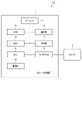
図1は、実施形態に係るICカード処理システム100の構成例を示す。図1が示すように、ICカード処理システム100は、ICカード処理装置1及びICカード2などを備える。ICカード処理装置1は、ICカード2と通信可能に接続する。 FIG. 1 shows a configuration example of an IC
なお、ICカード処理システム100は、図1が示すような構成の他に必要に応じた構成を具備したり、ICカード処理システム100から特定の構成が除外されたりしてもよい。 It should be noted that the IC
ICカード処理装置1(外部装置)は、ICカード処理システム100全体を制御する。ICカード処理装置1は、接触でICカード2に接続する。ICカード処理装置1は、ICカード2に対して電力を供給することでICカード2を活性化させる。また、ICカード処理装置1は、ICカード2に種々のコマンドを送信することで、ICカード2に種々の動作を実行させる。 The IC card processing device 1 (external device) controls the entire IC
図1が示すように、ICカード処理装置1は、プロセッサ11、ROM12、RAM13、NVM14、通信部15、操作部16、表示部17及びリーダライタ18などを備える。 As shown in FIG. 1, the IC
プロセッサ11と、ROM12、RAM13、NVM14、通信部15、操作部16、表示部17及びリーダライタ18と、は、データバスなどを介して互いに接続する。
なお、ICカード処理装置1は、図1が示すような構成の他に必要に応じた構成を具備したり、ICカード処理装置1から特定の構成が除外されたりしてもよい。The
The IC
プロセッサ11は、ICカード処理装置1全体の動作を制御する機能を有する。プロセッサ11は、内部キャッシュ及び各種のインターフェースなどを備えてもよい。プロセッサ11は、内部メモリ、ROM12又はNVM14が予め記憶するプログラムを実行することにより種々の処理を実現する。 The
なお、プロセッサ11がプログラムを実行することにより実現する各種の機能のうちの一部は、ハードウエア回路により実現されるものであってもよい。この場合、プロセッサ11は、ハードウエア回路により実行される機能を制御する。 Note that some of the various functions realized by the
ROM12は、制御プログラム及び制御データなどが予め記憶された不揮発性のメモリである。ROM12に記憶される制御プログラム及び制御データは、ICカード処理装置1の仕様に応じて予め組み込まれる。 The
RAM13は、揮発性のメモリである。RAM13は、プロセッサ11の処理中のデータなどを一時的に格納する。RAM13は、プロセッサ11からの命令に基づき種々のアプリケーションプログラムを格納する。また、RAM13は、アプリケーションプログラムの実行に必要なデータ及びアプリケーションプログラムの実行結果などを格納してもよい。
NVM14は、データの書き込み及び書き換えが可能な不揮発性のメモリである。NVM14は、たとえば、HDD(Hard Disk Drive)、SSD(Solid State Drive)又はフラッシュメモリなどから構成される。NVM14は、ICカード処理装置1の運用用途に応じて制御プログラム、アプリケーション及び種々のデータなどを格納する。 The NVM 14 is a non-volatile memory in which data can be written and rewritten. The NVM 14 is composed of, for example, an HDD (Hard Disk Drive), SSD (Solid State Drive), flash memory, or the like. The NVM 14 stores control programs, applications, various data, and the like according to the operational use of the IC
通信部15は、外部装置と通信するためのインターフェースである。即ち、通信部15は、ネットワークなどを通じて外部装置とデータを送受信するためのインターフェースである。たとえば、通信部15は、有線又は無線のLAN接続をサポートするインターフェースである。 The
操作部16は、オペレータから種々の操作の入力を受け付ける。操作部16は、入力された操作を示す信号をプロセッサ11へ送信する。操作部16は、タッチパネルから構成されてもよい。 The
表示部17は、プロセッサ11からの画像データを表示する。たとえば、表示部17は、液晶モニタから構成される。操作部16がタッチパネルから構成される場合、表示部17は、操作部16と一体的に形成されてもよい。 The
リーダライタ18は、ICカード2とデータを送受信するためのインターフェース装置である。リーダライタ18は、ICカード2と接触して通信を行うインターフェースにより構成される。たとえば、リーダライタ18は、ICカード2のコンタクト部と物理的かつ電気的に接続するための接触部などにより構成される。リーダライタ18は、ICカード2に対する電源供給、クロック供給、リセット制御及びデータの送受信などを行う。 The reader/
このような機能によってリーダライタ18は、プロセッサ11による制御に基づいてICカード2に対する電源供給、ICカード2の活性化(起動)、クロック供給、リセット制御、種々のコマンドの送信及び送信したコマンドに対する応答(レスポンス)の受信などを行なう。 With such functions, the reader/
ICカード2(携帯可能電子装置)は、ICカード処理装置1からのコマンドに従って動作する。ICカード2は、コマンドに対するレスポンスをICカード処理装置1に送信する。 The IC card 2 (portable electronic device) operates according to commands from the IC
ここでは、ICカード処理システム100は、ICカード2として、非接触通信のためのアンテナが互いに異なるICカード2a又はICカード2bの何れかを備える。 Here, the IC
まず、ICカード2aについて説明する。
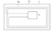
図2は、ICカード2aの構成例を示す。First, the
FIG. 2 shows a configuration example of the
図2が示すように、ICカード2aは、プラスチックなどで形成されたカード状の本体Sを有する。ICカード2aは、本体S内にICチップC及び第1のアンテナ30aなどを内蔵する。ICチップC及び第1のアンテナ30aは、互いに接続された状態で形成され、ICカード2aの本体S内に埋設される。ICチップCと第1のアンテナ30aとは、モジュールを形成する。 As shown in FIG. 2, the
第1のアンテナ30aは、非接触で上位装置と通信するアンテナである。第1のアンテナ30aは、非接触での通信をサポートするリーダライタに接続する。 The
第1のアンテナ30aは、所定のサイズ(フルサイズ)に形成されている。ここでは、第1のアンテナ30aは、本体Sの外周に沿って形成されている。第1のアンテナ30aは、第1のインダクタンスを有する。 The
ICチップC(LSI(Large Scale Integration))については、後述する。 The IC chip C (LSI (Large Scale Integration)) will be described later.
次に、ICカード2bについて説明する。
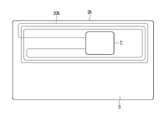
図3は、ICカード2bの構成例を示す。Next, the
FIG. 3 shows a configuration example of the
図3が示すように、ICカード2bは、プラスチックなどで形成されたカード状の本体Sを有する。ICカード2bは、本体S内にICチップC及び第2のアンテナ30bなどを内蔵する。ICチップC及び第2のアンテナ30bは、互いに接続された状態で形成され、ICカード2bの本体S内に埋設される。ICチップCと第2のアンテナ30bとは、モジュールを形成する。 As shown in FIG. 3, the
第2のアンテナ30bは、非接触で上位装置と通信するアンテナである。第2のアンテナ30bは、非接触での通信をサポートするリーダライタに接続する。 The
第2のアンテナ30bは、第1のアンテナ30aのサイズよりも小さいサイズ(ハーフサイズ)に形成されている。ここでは、第2のアンテナ30bは、本体Sの上側半分に形成されている。第2のアンテナ30bは、第1のインダクタンスよりも小さい第2のインダクタンスを有する。 The
なお、第1のアンテナ30a及び第2のアンテナ30bの形状は、ISO/IEC14443の規格に沿うものであってもよい。 The shapes of the
次に、ICチップCについて説明する。
図4は、ICチップCの構成例を示す。Next, the IC chip C will be explained.
FIG. 4 shows a configuration example of the IC chip C. As shown in FIG.
図4が示すように、ICチップCは、プロセッサ21、ROM22、RAM23、NVM24、接触通信部25、オンオフ回路26、アンテナ接続部27、スイッチ28及びコンデンサ29などを備える。プロセッサ21は、データバスなどを介してROM22、RAM23、NVM24、接触通信部25、オンオフ回路26及びアンテナ接続部27に接続する。オンオフ回路26は、スイッチ28に接続する。コンデンサ29は、スイッチ28を介してアンテナ接続部27に接続する。 As shown in FIG. 4, the IC chip C includes a
なお、ICチップCは、図4が示すような構成の他に必要に応じた構成を具備したり、ICチップCから特定の構成が除外されたりしてもよい。 In addition to the configuration shown in FIG. 4, the IC chip C may have a configuration according to need, or a specific configuration may be excluded from the IC chip C. FIG.
プロセッサ21は、ICカード2全体の制御を司る制御部として機能する。プロセッサ21は、ROM22又はNVM24に記憶される制御プログラム及び制御データに基づいて種々の処理を行う。たとえば、プロセッサ21は、ROM22に記憶されているプログラムを実行することにより、ICカード2の動作制御又はICカード2の運用形態に応じた種々の処理を行う。 The
たとえば、プロセッサ21は、プログラムを実行することにより、ICカード2内の各部の制御及び情報処理を実現するプロセッサであればよい。
なお、プロセッサ21がプログラムを実行することにより実現する各種の機能のうちの一部は、ハードウエア回路により実現されるものであっても良い。この場合、プロセッサ21は、ハードウエア回路により実行される機能を制御する。For example, the
Note that some of the various functions realized by the
ROM22は、予め制御用のプログラム及び制御データなどを記憶する不揮発性のメモリである。ROM22は、製造段階で制御プログラム及び制御データなどを記憶した状態でICカード2に組み込まれる。即ち、ROM22に記憶される制御プログラム及び制御データは、予めICカード2の仕様などに応じて組み込まれる。 The
RAM23は、揮発性のメモリである。RAM23は、プロセッサ21の処理中のデータなどを一時的に格納する。たとえば、RAM23は、計算用バッファ、受信用バッファ及び送信用バッファとして機能する。計算用バッファは、プロセッサ21が実行する種々の演算処理の結果などを一時的に保持する。受信用バッファは、接触通信部25などを介してリーダライタ18などから受信するコマンドデータなどを保持する。送信用バッファは、接触通信部25などを介してリーダライタ18などへ送信するメッセージ(レスポンス)などを保持する。
NVM24は、フラッシュROMなどのデータの書き込み及び書換えが可能な不揮発性のメモリにより構成される。NVM24は、ICカード2の運用用途に応じて制御プログラム、アプリケーション及び種々のデータを格納する。例えば、NVM24では、プログラムファイル及びデータファイルなどが作成される。作成された各ファイルは、制御プログラム及び種々のデータなどが書き込まれる。 The
接触通信部25(通信部)は、接触でリーダライタ18とデータを送受信するためのインターフェースである。即ち、接触通信部25は、リーダライタ18を通じてICカード処理装置1とデータを送受信するためのインターフェースである。 The contact communication unit 25 (communication unit) is an interface for transmitting and receiving data to and from the reader/
たとえば、接触通信部25は、リーダライタ18と物理的かつ電気的に接触して信号の送受信を行うための通信制御部とコンタクト部とにより構成される。たとえば、ICカード2は、コンタクト部を介してリーダライタ18からの動作電源及び動作クロックの供給を受けて活性化される。 For example, the
アンテナ接続部27は、第1のアンテナ30a又は第2のアンテナ30bに接続する。アンテナ接続部27は、第1のアンテナ30a又は第2のアンテナ30bから供給される電気信号をICチップC内に供給する。 The
ICチップCは、複数のコンデンサ29を備える。ここでは、ICチップCは、4つのコンデンサ29を備える。各コンデンサ29は、同一の容量を有するものであってもよいし、互いに異なる容量を有するものであってもよい。 IC chip C includes a plurality of
各コンデンサ29は、アンテナ接続部27に並列に接続する。即ち、各コンデンサ29は、第1のアンテナ30a又は第2のアンテナ30bに並列に接続する。 Each
各コンデンサ29は、ICチップCの内部コンデンサ容量を形成する。コンデンサ29と第1のアンテナ30a又は第2のアンテナ30bとは、共振回路を形成する。 Each
ICチップCは、複数のスイッチ28を備える。ここでは、ICチップCは、4つのスイッチ28を備える。 IC chip C includes a plurality of
各スイッチ28は、各コンデンサ29とアンテナ接続部27との間に形成される。即ち、各スイッチ28は、各コンデンサ29と第1のアンテナ30a又は第2のアンテナ30bとの接続を切り替える。
スイッチ28は、トランジスタなどから構成される。Each
The
オンオフ回路26(変更機構)は、プロセッサ21からの制御に従って各スイッチ28をオン又はオフに制御する。即ち、オンオフ回路26は、各コンデンサ29と第1のアンテナ30a又は第2のアンテナ30bとの接続を切り替える。オンオフ回路26は、各コンデンサ29と第1のアンテナ30a又は第2のアンテナ30bとの接続を切り替えることで、ICチップCの内部コンデンサ容量を変更する。 The on/off circuit 26 (change mechanism) controls each
たとえば、オンオフ回路26は、スイッチ28に電圧を印加し又は印加しないことでスイッチ28のオンオフを切り替える。 For example, on/off
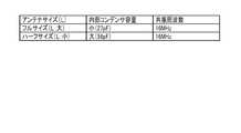
次に、アンテナサイズとICチップCの内部コンデンサ容量と共振周波数との関係について説明する。
図5は、アンテナサイズとICチップCの内部コンデンサ容量と共振周波数との関係を示す。Next, the relationship between the antenna size, the internal capacitance of the IC chip C, and the resonance frequency will be described.
FIG. 5 shows the relationship between the antenna size, the internal capacitor capacity of the IC chip C, and the resonance frequency.
共振周波数f0は、以下の式によって算出される。 The resonance frequency f0 is calculated by the following formula.

ここで、Lは、アンテナのインダクタンスを示し、Cは、内部コンデンサ容量を示す。 Here, L denotes the inductance of the antenna and C denotes the internal capacitor capacity.
また、ICカード2が上位装置と非接触で通信するために推奨される推奨共振周波数は、16Mhzであるものとする。 It is also assumed that the recommended resonant frequency for contactless communication between the
図5は、ICカード2の共振周波数(アンテナとICチップCとから構成される共振回路の共振周波数)が推奨共振周波数となるアンテナサイズと内部コンデンサ容量との組合せを示す。 FIG. 5 shows the combination of the antenna size and the internal capacitor capacity at which the resonant frequency of the IC card 2 (the resonant frequency of the resonant circuit composed of the antenna and the IC chip C) becomes the recommended resonant frequency.
図5が示すように、アンテナサイズがフルサイズ(第1のアンテナ30aのサイズ)である場合、内部コンデンサ容量は、27pFである。また、アンテナサイズがハーフサイズ(第2のアンテナ30bのサイズ)である場合、内部コンデンサ容量は、56pFである。 As shown in FIG. 5, when the antenna size is full size (the size of the
次に、ICカード処理装置1が実現する機能について説明する。ICカード処理装置が実現する機能は、プロセッサ11がROM12又はNVM14などに格納されるプログラムを実行することで実現される。 Next, functions realized by the IC
まず、プロセッサ11は、ICチップCの内部コンデンサ容量を取得する機能を有する。 First, the
ここでは、ICカード2は、リーダライタ18と通信可能な状態にセットされているものとする。 Here, it is assumed that the
プロセッサ11は、リーダライタ18を通じて、ICチップCの内部コンデンサ容量を取得するための取得コマンドをICカード2に送信する。 The
プロセッサ11は、リーダライタ18を通じて、内部コンデンサ容量を示すレスポンスをICカード2から受信する。 The
また、プロセッサ11は、ICチップCの内部コンデンサ容量を変更させる機能を有する。 The
ICチップCの内部コンデンサ容量を示すレスポンスを受信すると、プロセッサ11は、ICチップCの内部コンデンサ容量が適切であるかを判定する。即ち、プロセッサ11は、ICカード2の共振周波数が推奨共振周波数であるかを判定する。 Upon receiving the response indicating the internal capacitor capacity of the IC chip C, the
たとえば、NVM14は、各アンテナ(第1のアンテナ30a又は第2のアンテナ30b)に対応する内部コンデンサ容量(推奨容量)を予め格納する。推奨容量は、対応するアンテナと組み合わせた場合にICカード2の共振周波数が推奨共振周波数となるICチップCの内部コンデンサ容量である。 For example, the
プロセッサ11は、NVM14を参照して、ICカード2が備えるアンテナ(第1のアンテナ30a又は第2のアンテナ30b)に対応する推奨容量を取得する。推奨容量を取得すると、プロセッサ11は、ICチップCの内部コンデンサ容量と推奨容量とが整合(一致)するかを判定する。 The
両者が整合すると判定すると、プロセッサ11は、ICチップCの内部コンデンサ容量が適切であると判定する。 When determining that both match, the
また、両者がしないと判定すると、プロセッサ11は、ICチップCの内部コンデンサ容量が適切でないと判定する。 Also, if both determine that they do not, the
ICチップCの内部コンデンサ容量が適切でないと判定すると、プロセッサ11は、リーダライタ18を通じて、ICチップCの内部コンデンサ容量を推奨容量に変更させる変更コマンドを生成する。 When determining that the internal capacitor capacity of the IC chip C is not appropriate, the
変更コマンドは、目標の内部コンデンサ容量(ここでは、推奨容量)を示す。 The change command indicates the target internal capacitor capacity (here, recommended capacity).
たとえば、変更コマンドは、目標の内部コンデンサ容量を示すデータをAPDU部に格納する。この場合、変更コマンドは、目標の内部コンデンサ容量を示すデータをAPDU部のデータ部に格納してもよい。 For example, the change command stores data in the APDU portion indicating the target internal capacitor capacity. In this case, the change command may store data indicating the target internal capacitor capacity in the data portion of the APDU portion.
また、変更コマンドは、目標の内部コンデンサ容量を示すデータをヘッダ部に格納するものであってもよい。 Also, the change command may store data indicating the target internal capacitor capacity in the header portion.
また、変更コマンドは、アンチコリジョンシーケンス内のコマンド(たとえば、ATTRIB Higher layerなど)であってもよい。 Also, the change command may be a command within the anti-collision sequence (eg, ATTRIB Higher layer, etc.).
また、変更コマンドは、S-blockコマンドであってもよい。この場合、変更コマンドは、目標の内部コンデンサ容量を示すデータをRFUビットに格納してもよい。 Also, the change command may be an S-block command. In this case, the change command may store data in the RFU bit indicating the target internal capacitor capacity.
変更コマンドの構成は、特定の構成に限定されるものではない。 The configuration of the change command is not limited to any particular configuration.
変更コマンドを生成すると、プロセッサ11は、リーダライタ18を通じて、生成された変更コマンドをICカード2に送信する。 After generating the change command, the
プロセッサ11は、リーダライタ18を通じて、内部コンデンサ容量の変更が完了したことを示すレスポンス(完了通知)をICカード2から受信する。 The
なお、プロセッサ11は、操作部16を通じて、ICカード2が備えるアンテナを示す操作の入力を受け付けるものであってもよい。 Note that the
次に、ICカード2のICチップCが実現する機能について説明する。ICチップCが実現する機能は、プロセッサ21がROM22又はNVM24などに格納されるプログラムを実行することで実現される。 Next, functions realized by the IC chip C of the
まず、プロセッサ21は、ICチップCの内部コンデンサ容量をICカード処理装置1に通知する機能を有する。 First, the
ここでは、NVM24は、ICチップCの内部コンデンサ容量を示す容量情報を予め格納する。容量情報は、内部コンデンサ容量の値(F)を示す。また、容量情報は、各スイッチ28のオンオフ状態を示すものであってもよい。 Here, the
プロセッサ21は、接触通信部25を通じて、ICチップCの内部コンデンサ容量を取得するための取得コマンドをICカード処理装置1から受信する。取得コマンドを受信すると、プロセッサ21は、容量情報を参照して、ICチップCの内部コンデンサ容量を示すレスポンスを生成する。 The
レスポンスを生成すると、プロセッサ21は、接触通信部25を通じて、生成されたレスポンスをICカード処理装置1に送信する。 After generating the response, the
また、プロセッサ21は、ICチップCの内部コンデンサ容量を変更する機能を有する。 The
プロセッサ21は、接触通信部25を通じて、変更コマンドをICカード処理装置1から受信する。変更コマンドを受信すると、プロセッサ21は、変更コマンドから目標の内部コンデンサ容量を取得する。 The
目標の内部コンデンサ容量を取得すると、プロセッサ21は、ICチップCの内部コンデンサ容量が目標の内部コンデンサ容量となるようにオンオフ回路26を制御する。即ち、プロセッサ21は、各スイッチ28をオンオフ制御して選択的に各コンデンサ29をアンテナに接続する。 After acquiring the target internal capacitor capacity, the
また、プロセッサ21は、容量情報を更新する。即ち、プロセッサ21は、現在の容量情報に目標の内部コンデンサ容量を示す容量情報を上書きする。 Also, the
各スイッチ28のオンオフ制御及び容量情報の更新が完了すると、プロセッサ21は、接触通信部25を通じて、内部コンデンサ容量の変更が完了したことを示すレスポンス(完了通知)をICカード処理装置1に送信する。 When the ON/OFF control of each
なお、ICチップCは、起動時において容量情報が示す内部コンデンサ容量を有する。たとえば、プロセッサ21は、起動時において容量情報に従ってオンオフ回路26を制御して、容量情報が示す内部コンデンサ容量を実現する。 It should be noted that the IC chip C has an internal capacitor capacity indicated by the capacity information at startup. For example, the
また、オンオフ回路26のオンオフ制御は、ICチップCの非活性化時においても維持されるものであってもよい。 Also, the on/off control of the on/off
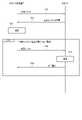
次に、ICカード処理システム100の動作例について説明する。
たとえば、ICカード処理システム100は、一次発行において以下の動作を行う。Next, an operation example of the IC
For example, the IC
ここでは、ICカード2は、リーダライタ18に通信可能な状態にセットされているものとする。 Here, it is assumed that the
まず、ICカード処理装置1のプロセッサ11は、リーダライタ18を通じて内部コンデンサ容量を取得するための取得コマンドをICカード2に送信する(S11)。 First, the
ICカード2のプロセッサ21は、接触通信部25を通じて当該取得コマンドを受信する。当該取得コマンドを取得すると、プロセッサ21は、接触通信部25を通じてICチップCの内部コンデンサ容量を示すレスポンスをICカード処理装置1に送信する(S12)。 The
ICカード処理装置1のプロセッサ11は、リーダライタ18を通じて当該レスポンスを受信する。当該レスポンスを受信すると、プロセッサ11は、当該レスポンスが示す内部コンデンサ容量が適切であるかを判定する(S13)。 The
当該レスポンスが示す内部コンデンサ容量が適切でないと判定すると(S13、NO)、プロセッサ11は、リーダライタ18を通じて目標の内部コンデンサ容量として推奨容量を示す変更コマンドをICカード2に送信する(S14)。 When determining that the internal capacitor capacity indicated by the response is not appropriate (S13, NO), the
ICカード2のプロセッサ21は、接触通信部25を通じて当該変更コマンドを受信する。当該変更コマンドを取得すると、プロセッサ21は、当該変更コマンドに従ってICチップCの内部コンデンサ容量を変更する(S15)。
ICチップCの内部コンデンサ容量を変更すると、プロセッサ21は、接触通信部25を通じて完了通知をICカード処理装置1に送信する(S16)。 After changing the internal capacitor capacity of the IC chip C, the
ICカード処理装置1のプロセッサ11は、当該完了通知を受信する。プロセッサ11が当該完了通知を受信した場合、又は内部コンデンサ容量が適切あると判定した場合(S13、YES)、ICカード処理システム100は、動作を終了する。 The
なお、ICカード処理装置1及びICカード2は、S11又はS14の前に相互認証を行ってもよい。 Note that the IC
また、ICカード2のNVM24は、容量情報を格納しなくともよい。この場合、プロセッサ21は、各スイッチ28のオンオフ状態に従ってICチップCの内部コンデンサ容量を取得してもよい。 Also, the
また、コンデンサ29は、ICチップCの外に形成されるものであってもよい。たとえば、コンデンサ29は、本体S内に形成されるものであってもよい。 Also, the
以上のように構成されたICカード処理システムは、ICカードが備えるアンテナに応じてICチップの内部コンデンサ容量を変更することができる。その結果、ICカード処理システムは、アンテナの種類に関わらず、同一のICチップを有するICカードの共振周波数を所定の周波数に設定することができる。 The IC card processing system configured as described above can change the internal capacitor capacity of the IC chip according to the antenna provided in the IC card. As a result, the IC card processing system can set the resonance frequency of IC cards having the same IC chip to a predetermined frequency regardless of the type of antenna.
本発明のいくつかの実施形態を説明したが、これらの実施形態は、例として提示したものであり、発明の範囲を限定することは意図していない。これら新規な実施形態は、その他の様々な形態で実施されることが可能であり、発明の要旨を逸脱しない範囲で、種々の省略、置き換え、変更を行うことができる。これら実施形態やその変形は、発明の範囲や要旨に含まれるとともに、特許請求の範囲に記載された発明とその均等の範囲に含まれる。 While several embodiments of the invention have been described, these embodiments have been presented by way of example and are not intended to limit the scope of the invention. These novel embodiments can be implemented in various other forms, and various omissions, replacements, and modifications can be made without departing from the scope of the invention. These embodiments and modifications thereof are included in the scope and gist of the invention, and are included in the scope of the invention described in the claims and equivalents thereof.
1…ICカード処理装置、2…ICカード、2a…ICカード、2b…ICカード、11…プロセッサ、12…ROM、13…RAM、14…NVM、15…通信部、16…操作部、17…表示部、18…リーダライタ、21…プロセッサ、22…ROM、23…RAM、24…NVM、25…接触通信部、26…オンオフ回路、27…アンテナ接続部、28…スイッチ、29…コンデンサ、30a…第1のアンテナ、30b…第2のアンテナ、100…ICカード処理システム、C…ICチップ、S…本体。 DESCRIPTION OF
Claims (9)
Translated fromJapanese非接触で通信するアンテナと、
前記アンテナに接続するコンデンサと、
前記コンデンサの容量を変更する変更機構と、
前記通信部を通じて、前記容量を変更させる変更コマンドを前記外部装置から受信し、
前記変更機構を用いて、前記変更コマンドに従って前記容量を変更する、
プロセッサと、
を備えるICカード。a communication unit that transmits and receives data to and from an external device;
an antenna for contactless communication;
a capacitor connected to the antenna;
a changing mechanism for changing the capacity of the capacitor;
receiving a change command for changing the capacity from the external device through the communication unit;
using the change mechanism to change the capacity according to the change command;
a processor;
IC card with
前記変更機構は、前記スイッチをオンオフ制御する、
請求項1に記載のICカード。a switch formed between the antenna and the capacitor;
The change mechanism turns on and off the switch,
The IC card according to claim 1.
前記コンデンサは、前記アンテナに並列に接続する、
請求項1又は2に記載のICカード。comprising a plurality of said capacitors,
the capacitor is connected in parallel to the antenna;
The IC card according to claim 1 or 2.
請求項1乃至3の何れか1項に記載のICカード。The communication unit transmits and receives data to and from the external device by contact.
The IC card according to any one of claims 1 to 3.
前記通信部を通じて、前記容量を取得するための取得コマンドを前記外部装置から受信し、
前記通信部を通じて、前記容量を示すレスポンスを前記外部装置に送信する、
請求項1乃至4の何れか1項に記載のICカード。The processor
receiving an acquisition command for acquiring the capacity from the external device through the communication unit;
Transmitting a response indicating the capacity to the external device through the communication unit;
The IC card according to any one of claims 1 to 4.
請求項1乃至5の何れか1項に記載のICカード。The processor changes the capacitance so that a resonance frequency of a resonance circuit composed of the antenna and the capacitor becomes a predetermined frequency.
The IC card according to any one of claims 1 to 5.
前記モジュールを内蔵した本体と、
を備えるICカード。a communication unit for transmitting and receiving data to and from an external device, an antenna for contactless communication, a capacitor connected to the antenna, a change mechanism for changing the capacity of the capacitor, and a change command for changing the capacity through the communication unit. from the external device and uses the modification mechanism to modify the capacity in accordance with the modification command;
a body containing the module;
IC card with
非接触で通信するアンテナと、
前記アンテナに接続するコンデンサと、
前記コンデンサの容量を変更する変更機構と、
前記通信部を通じて、前記容量を変更させる変更コマンドを前記外部装置から受信し、
前記変更機構を用いて、前記変更コマンドに従って前記容量を変更する、
プロセッサと、
を備える携帯可能電子装置。a communication unit that transmits and receives data to and from an external device;
an antenna for contactless communication;
a capacitor connected to the antenna;
a changing mechanism for changing the capacity of the capacitor;
receiving a change command for changing the capacity from the external device through the communication unit;
using the change mechanism to change the capacity according to the change command;
a processor;
A portable electronic device comprising:
前記通信部を通じて、内部コンデンサ容量を前記ICカードのアンテナに対応する容量に変更させる変更コマンドを前記ICカードに送信するプロセッサと、
を備えるICカード処理装置。
a communication unit that transmits and receives data to and from the IC card;
a processor that transmits to the IC card, through the communication unit, a change command for changing an internal capacitor capacity to a capacity corresponding to an antenna of the IC card;
IC card processing device.
Priority Applications (1)
| Application Number | Priority Date | Filing Date | Title |
|---|---|---|---|
| JP2021044884AJP2022144044A (en) | 2021-03-18 | 2021-03-18 | IC card, portable electronic device and IC card processing device |
Applications Claiming Priority (1)
| Application Number | Priority Date | Filing Date | Title |
|---|---|---|---|
| JP2021044884AJP2022144044A (en) | 2021-03-18 | 2021-03-18 | IC card, portable electronic device and IC card processing device |
Publications (1)
| Publication Number | Publication Date |
|---|---|
| JP2022144044Atrue JP2022144044A (en) | 2022-10-03 |
Family
ID=83454505
Family Applications (1)
| Application Number | Title | Priority Date | Filing Date |
|---|---|---|---|
| JP2021044884APendingJP2022144044A (en) | 2021-03-18 | 2021-03-18 | IC card, portable electronic device and IC card processing device |
Country Status (1)
| Country | Link |
|---|---|
| JP (1) | JP2022144044A (en) |
- 2021
- 2021-03-18JPJP2021044884Apatent/JP2022144044A/enactivePending
Similar Documents
| Publication | Publication Date | Title |
|---|---|---|
| JP4685926B2 (en) | Improved transponder | |
| US8931705B2 (en) | IC card, mobile electronic device and data processing method in IC card | |
| AU2018445738A1 (en) | Memory card, memory card adapter, and terminal device | |
| US10032105B2 (en) | IC card, portable terminal, and portable electronic apparatus | |
| TW201701195A (en) | Dual frequency HF-UHF identification device, in particular of the passive type | |
| US10810480B2 (en) | Electronic tag and electronic system using the same | |
| US10498671B2 (en) | IC card, portable electronic apparatus, and IC card processing apparatus | |
| JP2022144044A (en) | IC card, portable electronic device and IC card processing device | |
| JP2017126125A (en) | IC card, portable electronic device and processing device | |
| KR101739522B1 (en) | Apparatus and method for firmware update using nfc bridge circuit supporting | |
| US20120234926A1 (en) | Portable electronic apparatus | |
| JP6181018B2 (en) | IC card, IC module, and portable terminal | |
| JP2015125627A (en) | IC card and portable electronic device | |
| JP2016212779A (en) | Portable electronic device and IC card | |
| JP2021114146A (en) | Control programs for IC cards, IC card processing systems, and IC card processing devices | |
| JP6828246B2 (en) | Electronic information storage media, information processing methods, and information processing programs | |
| JP2005275456A (en) | Portable electronic medium, integrated circuit used for portable electronic medium, and method for issuing portable electronic medium | |
| JP2018097470A (en) | Ic card, portable electronic device and processor | |
| JP7433886B2 (en) | IC cards and IC card control programs | |
| JP2025103789A (en) | Portable electronic device and IC card | |
| JP2018101252A (en) | Ic card, portable electronic device, and processing device | |
| JP2016126441A (en) | Portable electronic device | |
| JP6461759B2 (en) | IC card and IC module | |
| JP2020205120A (en) | Electronic information storage medium, information processing method, and information processing program | |
| CN101599020B (en) | Method for downloading and executing program codes from microprocessor and communication device thereof |
Legal Events
| Date | Code | Title | Description |
|---|---|---|---|
| RD01 | Notification of change of attorney | Free format text:JAPANESE INTERMEDIATE CODE: A7421 Effective date:20230105 |