JP2022140574A - Beam guidance system based on MEMS-actuated vertical coupler array - Google Patents
Beam guidance system based on MEMS-actuated vertical coupler arrayDownload PDFInfo
- Publication number
- JP2022140574A JP2022140574AJP2022118719AJP2022118719AJP2022140574AJP 2022140574 AJP2022140574 AJP 2022140574AJP 2022118719 AJP2022118719 AJP 2022118719AJP 2022118719 AJP2022118719 AJP 2022118719AJP 2022140574 AJP2022140574 AJP 2022140574A
- Authority
- JP
- Japan
- Prior art keywords
- coupler
- waveguide
- row
- optical
- waveguides
- Prior art date
- Legal status (The legal status is an assumption and is not a legal conclusion. Google has not performed a legal analysis and makes no representation as to the accuracy of the status listed.)
- Granted
Links
Images


Classifications
- G—PHYSICS
- G01—MEASURING; TESTING
- G01S—RADIO DIRECTION-FINDING; RADIO NAVIGATION; DETERMINING DISTANCE OR VELOCITY BY USE OF RADIO WAVES; LOCATING OR PRESENCE-DETECTING BY USE OF THE REFLECTION OR RERADIATION OF RADIO WAVES; ANALOGOUS ARRANGEMENTS USING OTHER WAVES
- G01S7/00—Details of systems according to groups G01S13/00, G01S15/00, G01S17/00
- G01S7/48—Details of systems according to groups G01S13/00, G01S15/00, G01S17/00 of systems according to group G01S17/00
- G01S7/481—Constructional features, e.g. arrangements of optical elements
- G01S7/4817—Constructional features, e.g. arrangements of optical elements relating to scanning
- G—PHYSICS
- G02—OPTICS
- G02F—OPTICAL DEVICES OR ARRANGEMENTS FOR THE CONTROL OF LIGHT BY MODIFICATION OF THE OPTICAL PROPERTIES OF THE MEDIA OF THE ELEMENTS INVOLVED THEREIN; NON-LINEAR OPTICS; FREQUENCY-CHANGING OF LIGHT; OPTICAL LOGIC ELEMENTS; OPTICAL ANALOGUE/DIGITAL CONVERTERS
- G02F1/00—Devices or arrangements for the control of the intensity, colour, phase, polarisation or direction of light arriving from an independent light source, e.g. switching, gating or modulating; Non-linear optics
- G02F1/29—Devices or arrangements for the control of the intensity, colour, phase, polarisation or direction of light arriving from an independent light source, e.g. switching, gating or modulating; Non-linear optics for the control of the position or the direction of light beams, i.e. deflection
- G02F1/292—Devices or arrangements for the control of the intensity, colour, phase, polarisation or direction of light arriving from an independent light source, e.g. switching, gating or modulating; Non-linear optics for the control of the position or the direction of light beams, i.e. deflection by controlled diffraction or phased-array beam steering
- E—FIXED CONSTRUCTIONS
- E06—DOORS, WINDOWS, SHUTTERS, OR ROLLER BLINDS IN GENERAL; LADDERS
- E06B—FIXED OR MOVABLE CLOSURES FOR OPENINGS IN BUILDINGS, VEHICLES, FENCES OR LIKE ENCLOSURES IN GENERAL, e.g. DOORS, WINDOWS, BLINDS, GATES
- E06B9/00—Screening or protective devices for wall or similar openings, with or without operating or securing mechanisms; Closures of similar construction
- E06B9/56—Operating, guiding or securing devices or arrangements for roll-type closures; Spring drums; Tape drums; Counterweighting arrangements therefor
- E06B9/80—Safety measures against dropping or unauthorised opening; Braking or immobilising devices; Devices for limiting unrolling
- E—FIXED CONSTRUCTIONS
- E06—DOORS, WINDOWS, SHUTTERS, OR ROLLER BLINDS IN GENERAL; LADDERS
- E06B—FIXED OR MOVABLE CLOSURES FOR OPENINGS IN BUILDINGS, VEHICLES, FENCES OR LIKE ENCLOSURES IN GENERAL, e.g. DOORS, WINDOWS, BLINDS, GATES
- E06B9/00—Screening or protective devices for wall or similar openings, with or without operating or securing mechanisms; Closures of similar construction
- E06B9/24—Screens or other constructions affording protection against light, especially against sunshine; Similar screens for privacy or appearance; Slat blinds
- E06B9/26—Lamellar or like blinds, e.g. venetian blinds
- E06B9/28—Lamellar or like blinds, e.g. venetian blinds with horizontal lamellae, e.g. non-liftable
- E06B9/30—Lamellar or like blinds, e.g. venetian blinds with horizontal lamellae, e.g. non-liftable liftable
- E06B9/32—Operating, guiding, or securing devices therefor
- E06B9/325—Immobilising devices preventing raising
- E—FIXED CONSTRUCTIONS
- E06—DOORS, WINDOWS, SHUTTERS, OR ROLLER BLINDS IN GENERAL; LADDERS
- E06B—FIXED OR MOVABLE CLOSURES FOR OPENINGS IN BUILDINGS, VEHICLES, FENCES OR LIKE ENCLOSURES IN GENERAL, e.g. DOORS, WINDOWS, BLINDS, GATES
- E06B9/00—Screening or protective devices for wall or similar openings, with or without operating or securing mechanisms; Closures of similar construction
- E06B9/24—Screens or other constructions affording protection against light, especially against sunshine; Similar screens for privacy or appearance; Slat blinds
- E06B9/26—Lamellar or like blinds, e.g. venetian blinds
- E06B9/28—Lamellar or like blinds, e.g. venetian blinds with horizontal lamellae, e.g. non-liftable
- E06B9/30—Lamellar or like blinds, e.g. venetian blinds with horizontal lamellae, e.g. non-liftable liftable
- E06B9/32—Operating, guiding, or securing devices therefor
- E06B9/326—Details of cords, e.g. buckles, drawing knobs
- E—FIXED CONSTRUCTIONS
- E06—DOORS, WINDOWS, SHUTTERS, OR ROLLER BLINDS IN GENERAL; LADDERS
- E06B—FIXED OR MOVABLE CLOSURES FOR OPENINGS IN BUILDINGS, VEHICLES, FENCES OR LIKE ENCLOSURES IN GENERAL, e.g. DOORS, WINDOWS, BLINDS, GATES
- E06B9/00—Screening or protective devices for wall or similar openings, with or without operating or securing mechanisms; Closures of similar construction
- E06B9/24—Screens or other constructions affording protection against light, especially against sunshine; Similar screens for privacy or appearance; Slat blinds
- E06B9/26—Lamellar or like blinds, e.g. venetian blinds
- E06B9/28—Lamellar or like blinds, e.g. venetian blinds with horizontal lamellae, e.g. non-liftable
- E06B9/34—Lamellar or like blinds, e.g. venetian blinds with horizontal lamellae, e.g. non-liftable roller-type; Roller shutters with adjustable lamellae
- E—FIXED CONSTRUCTIONS
- E06—DOORS, WINDOWS, SHUTTERS, OR ROLLER BLINDS IN GENERAL; LADDERS
- E06B—FIXED OR MOVABLE CLOSURES FOR OPENINGS IN BUILDINGS, VEHICLES, FENCES OR LIKE ENCLOSURES IN GENERAL, e.g. DOORS, WINDOWS, BLINDS, GATES
- E06B9/00—Screening or protective devices for wall or similar openings, with or without operating or securing mechanisms; Closures of similar construction
- E06B9/24—Screens or other constructions affording protection against light, especially against sunshine; Similar screens for privacy or appearance; Slat blinds
- E06B9/40—Roller blinds
- E06B9/42—Parts or details of roller blinds, e.g. suspension devices, blind boxes
- G—PHYSICS
- G02—OPTICS
- G02B—OPTICAL ELEMENTS, SYSTEMS OR APPARATUS
- G02B26/00—Optical devices or arrangements for the control of light using movable or deformable optical elements
- G02B26/08—Optical devices or arrangements for the control of light using movable or deformable optical elements for controlling the direction of light
- G02B26/0816—Optical devices or arrangements for the control of light using movable or deformable optical elements for controlling the direction of light by means of one or more reflecting elements
- G02B26/0833—Optical devices or arrangements for the control of light using movable or deformable optical elements for controlling the direction of light by means of one or more reflecting elements the reflecting element being a micromechanical device, e.g. a MEMS mirror, DMD
- G—PHYSICS
- G02—OPTICS
- G02B—OPTICAL ELEMENTS, SYSTEMS OR APPARATUS
- G02B26/00—Optical devices or arrangements for the control of light using movable or deformable optical elements
- G02B26/08—Optical devices or arrangements for the control of light using movable or deformable optical elements for controlling the direction of light
- G02B26/10—Scanning systems
- G—PHYSICS
- G02—OPTICS
- G02B—OPTICAL ELEMENTS, SYSTEMS OR APPARATUS
- G02B6/00—Light guides; Structural details of arrangements comprising light guides and other optical elements, e.g. couplings
- G02B6/10—Light guides; Structural details of arrangements comprising light guides and other optical elements, e.g. couplings of the optical waveguide type
- G02B6/12—Light guides; Structural details of arrangements comprising light guides and other optical elements, e.g. couplings of the optical waveguide type of the integrated circuit kind
- G02B6/122—Basic optical elements, e.g. light-guiding paths
- G—PHYSICS
- G02—OPTICS
- G02B—OPTICAL ELEMENTS, SYSTEMS OR APPARATUS
- G02B6/00—Light guides; Structural details of arrangements comprising light guides and other optical elements, e.g. couplings
- G02B6/24—Coupling light guides
- G02B6/26—Optical coupling means
- G02B6/35—Optical coupling means having switching means
- G02B6/354—Switching arrangements, i.e. number of input/output ports and interconnection types
- G—PHYSICS
- G02—OPTICS
- G02F—OPTICAL DEVICES OR ARRANGEMENTS FOR THE CONTROL OF LIGHT BY MODIFICATION OF THE OPTICAL PROPERTIES OF THE MEDIA OF THE ELEMENTS INVOLVED THEREIN; NON-LINEAR OPTICS; FREQUENCY-CHANGING OF LIGHT; OPTICAL LOGIC ELEMENTS; OPTICAL ANALOGUE/DIGITAL CONVERTERS
- G02F1/00—Devices or arrangements for the control of the intensity, colour, phase, polarisation or direction of light arriving from an independent light source, e.g. switching, gating or modulating; Non-linear optics
- G02F1/29—Devices or arrangements for the control of the intensity, colour, phase, polarisation or direction of light arriving from an independent light source, e.g. switching, gating or modulating; Non-linear optics for the control of the position or the direction of light beams, i.e. deflection
- G02F1/295—Analog deflection from or in an optical waveguide structure]
- G—PHYSICS
- G02—OPTICS
- G02F—OPTICAL DEVICES OR ARRANGEMENTS FOR THE CONTROL OF LIGHT BY MODIFICATION OF THE OPTICAL PROPERTIES OF THE MEDIA OF THE ELEMENTS INVOLVED THEREIN; NON-LINEAR OPTICS; FREQUENCY-CHANGING OF LIGHT; OPTICAL LOGIC ELEMENTS; OPTICAL ANALOGUE/DIGITAL CONVERTERS
- G02F1/00—Devices or arrangements for the control of the intensity, colour, phase, polarisation or direction of light arriving from an independent light source, e.g. switching, gating or modulating; Non-linear optics
- G02F1/29—Devices or arrangements for the control of the intensity, colour, phase, polarisation or direction of light arriving from an independent light source, e.g. switching, gating or modulating; Non-linear optics for the control of the position or the direction of light beams, i.e. deflection
- G02F1/31—Digital deflection, i.e. optical switching
- G02F1/313—Digital deflection, i.e. optical switching in an optical waveguide structure
- G02F1/3132—Digital deflection, i.e. optical switching in an optical waveguide structure of directional coupler type
- G—PHYSICS
- G02—OPTICS
- G02F—OPTICAL DEVICES OR ARRANGEMENTS FOR THE CONTROL OF LIGHT BY MODIFICATION OF THE OPTICAL PROPERTIES OF THE MEDIA OF THE ELEMENTS INVOLVED THEREIN; NON-LINEAR OPTICS; FREQUENCY-CHANGING OF LIGHT; OPTICAL LOGIC ELEMENTS; OPTICAL ANALOGUE/DIGITAL CONVERTERS
- G02F1/00—Devices or arrangements for the control of the intensity, colour, phase, polarisation or direction of light arriving from an independent light source, e.g. switching, gating or modulating; Non-linear optics
- G02F1/29—Devices or arrangements for the control of the intensity, colour, phase, polarisation or direction of light arriving from an independent light source, e.g. switching, gating or modulating; Non-linear optics for the control of the position or the direction of light beams, i.e. deflection
- G02F1/31—Digital deflection, i.e. optical switching
- G02F1/313—Digital deflection, i.e. optical switching in an optical waveguide structure
- G02F1/3137—Digital deflection, i.e. optical switching in an optical waveguide structure with intersecting or branching waveguides, e.g. X-switches and Y-junctions
- G—PHYSICS
- G02—OPTICS
- G02F—OPTICAL DEVICES OR ARRANGEMENTS FOR THE CONTROL OF LIGHT BY MODIFICATION OF THE OPTICAL PROPERTIES OF THE MEDIA OF THE ELEMENTS INVOLVED THEREIN; NON-LINEAR OPTICS; FREQUENCY-CHANGING OF LIGHT; OPTICAL LOGIC ELEMENTS; OPTICAL ANALOGUE/DIGITAL CONVERTERS
- G02F2203/00—Function characteristic
- G02F2203/24—Function characteristic beam steering
Landscapes
- Physics & Mathematics (AREA)
- Nonlinear Science (AREA)
- General Physics & Mathematics (AREA)
- Optics & Photonics (AREA)
- Engineering & Computer Science (AREA)
- Structural Engineering (AREA)
- Architecture (AREA)
- Civil Engineering (AREA)
- Radar, Positioning & Navigation (AREA)
- Remote Sensing (AREA)
- Computer Networks & Wireless Communication (AREA)
- Microelectronics & Electronic Packaging (AREA)
- Mechanical Light Control Or Optical Switches (AREA)
- Optical Couplings Of Light Guides (AREA)
- Optical Communication System (AREA)
Abstract
Translated fromJapaneseDescription
Translated fromJapanese関連出願の相互参照
本事例は、参照により本明細書に組み込まれる、2018年6月19日に出願された米国仮特許出願第62/686,848号(代理人整理番号:332-007PR1)の利益を主張する。CROSS REFERENCE TO RELATED APPLICATIONS This case is of U.S. Provisional Patent Application No. 62/686,848 (Attorney Docket Number: 332-007PR1), filed June 19, 2018, which is incorporated herein by reference. claim profit.
本事例における主張の解釈に影響を及ぼす可能性がある、本出願と、参照により組み込まれている事例との間の言語における矛盾または不一致が存在する場合、本事例における主張は、本事例における言語と一致するものと解釈されるべきである。 Where there is a conflict or inconsistency in language between this application and any case incorporated by reference that may affect the interpretation of the claim in this case, the claim in this case shall be should be construed as consistent with
連邦政府委託研究に関する記載
本発明は、先端研究プロジェクト庁-エネルギー(Advanced Research Projects Agency-Energy)(ARPA-E)によって授与された契約番号DE-AR0000849のもとで米国政府の支援によってなされた。米国政府は、本発明に一定の権利を有する。STATEMENT REGARDING FEDERALLY SPONSORED RESEARCH This invention was made with US Government support under Contract No. DE-AR0000849 awarded by the Advanced Research Projects Agency-Energy (ARPA-E). The United States Government has certain rights in this invention.
本開示は、一般に、自由空間光通信に関し、より詳細には、自由空間ビーム誘導に関する。 TECHNICAL FIELD This disclosure relates generally to free-space optical communications, and more particularly to free-space beam steering.
アジャイルビーム誘導デバイスは、自由空間光通信だけでなく、LiDAR(光検出と測距)、3Dイメージング、センシング、および顕微鏡用途のために必要とされる。それらのデバイスは、スキャニングおよび取得/ポインティング/追跡(ATP)機能を提供する。伝統的なビーム誘導装置は、モータ駆動の機械的ジンバルを使用して、光学系全体を回転させる。不都合点として、モータ駆動のジンバルは、かさ高く、重く、かつ大量の電力を消費する。 Agile beam steering devices are needed for LiDAR (light detection and ranging), 3D imaging, sensing, and microscopy applications, as well as free-space optical communications. These devices provide scanning and acquisition/pointing/tracking (ATP) capabilities. Traditional beam steering devices use a motor-driven mechanical gimbal to rotate the entire optical system. Disadvantageously, motorized gimbals are bulky, heavy, and consume large amounts of power.
集積されたビーム誘導システムは、ポータブルまたはモバイルのプラットフォームにおいて高い有用性を示し、「ソリッドステートLiDAR」の主要な要素になった。たとえば、コリメーションおよびビーム誘導は、従来技術では、レンズ(たとえば、テレセントリックレンズ、望遠鏡など)の焦点面に配置された光源を使用して、ならびにレンズの光軸の位置およびレンズの焦点面の中の光源の位置の配列を変えて実証されてきた。これは、光軸に対してマクロ光源(macro light source)を動かすこと、焦点面の中に配置された光ファイバを動かすこと、および固定位置の光源に対してレンズを動かすことなどによって、様々な方法で行われてきた。 Integrated beam steering systems have shown high utility in portable or mobile platforms and have become a key component of 'solid-state LiDAR'. For example, collimation and beam steering are conventionally accomplished using a light source positioned at the focal plane of a lens (e.g., telecentric lens, telescope, etc.) and at the position of the optical axis of the lens and within the focal plane of the lens. It has been demonstrated with different arrangements of the positions of the light sources. This can be done in a variety of ways, such as by moving the macro light source with respect to the optical axis, moving an optical fiber placed in the focal plane, and moving a lens with respect to a fixed position light source. method has been done.
不都合点として、レンズおよび/または光源を動かすために必要な機械システムは、負荷の重量/剛性に起因して制限された周波数応答を有し、LiDARおよび/または高速移動車両の間の自由空間通信に対してあまりに遅く、かつかさ高く、複雑で、遅くて高価である。 As a disadvantage, the mechanical system required to move the lens and/or light source has a limited frequency response due to the weight/stiffness of the load, making free-space communication between LiDAR and/or fast-moving vehicles too slow, bulky, complex, slow and expensive for
他の従来技術のビーム誘導システムは、垂直共振器面発光レーザ(VCSEL:vertical cavity surface-emitting lasers)の2次元(2D)配列の個々の素子を選択的に励起する電子クロスバースイッチに基づく。しかしながら、そのような手法は、レーザの大きい配列を必要とする。加えて、そのようなシステムは、VCSEL源を必要とし、それは、いくつかの通信またはセンシングの用途に対してあまり適さない。 Other prior art beam steering systems are based on electronic crossbar switches that selectively excite individual elements of a two-dimensional (2D) array of vertical cavity surface-emitting lasers (VCSELs). However, such an approach requires large arrays of lasers. Additionally, such systems require a VCSEL source, which is not well suited for some communication or sensing applications.
さらに他の従来技術のビーム誘導システムは、シリコンフォトニックベースの熱光学スイッチを使用して、面発光格子カプラ(surface-emitting grating coupler)を活性化している。不都合点として、熱光学スイッチは、温度に敏感であり、制限された誘導能力を有し、高い電力消費量を有し、大規模ビーム誘導デバイスに対して適切に縮小拡張できない。 Yet another prior art beam steering system uses a silicon photonic-based thermo-optic switch to activate a surface-emitting grating coupler. As disadvantages, thermo-optic switches are temperature sensitive, have limited steering capabilities, have high power consumption, and do not scale well for large scale beam steering devices.
実際的なビーム誘導技術は、いまだ、従来技術において利用できないままである。 Practical beam steering techniques still remain unavailable in the prior art.
本開示は、レンズの焦点面の中に配置された機械的にアクティブな垂直格子カプラ(すなわち、カプラ)の集積された光学ベースのプログラマブル2次元(2D)配列を含むビーム誘導装置を対象とする。レンズは、カプラのいずれかによって放射される自由空間光を、コリメートされた自由空間光ビームに変換するように配列される。プログラマブルカプラ配列は、基板上にモノリシックに集積され、どのカプラ(または複数のカプラ)が励起される(すなわち、光を受信して光を自由空間に放出する)かを制御するスイッチングネットワークを含む。スイッチングネットワークは、励起されないカプラへの漏洩を軽減し、それにより、光学的クロストークを軽減するように構成される。各自由空間光ビームの伝搬方向(すなわち、レンズの光軸に対するその出力角)は、レンズの光軸に対するそのそれぞれのカプラのx座標とy座標の関数である。本開示による実施形態は、LiDARシステム、光通信システム、光干渉断層計および他の医用イメージングシステム、3次元イメージングおよびセンシング用途などにおける使用に対して特によく適する。 The present disclosure is directed to a beam steering apparatus that includes an integrated optics-based programmable two-dimensional (2D) array of mechanically active vertical grating couplers (i.e., couplers) positioned in the focal plane of a lens. . A lens is arranged to convert free-space light emitted by either of the couplers into a collimated free-space light beam. A programmable coupler array is monolithically integrated on a substrate and includes a switching network that controls which coupler (or couplers) is excited (i.e., receives light and emits light into free space). The switching network is configured to mitigate leakage into unexcited couplers, thereby mitigating optical crosstalk. The direction of propagation of each free-space light beam (ie, its output angle with respect to the optical axis of the lens) is a function of the x- and y-coordinates of its respective coupler with respect to the optical axis of the lens. Embodiments according to the present disclosure are particularly well suited for use in LiDAR systems, optical communication systems, optical coherence tomography and other medical imaging systems, three-dimensional imaging and sensing applications, and the like.
本開示による例示的な実施形態は、レンズと、(1)機械的にアクティブな集積された光学ベースのカプラの2次元配列および(2)どのカプラが励起されるかを制御するための集積された光学ベースのスイッチングネットワークを含むプログラマブル垂直カプラ配列とを含むビーム誘導システムである。 Exemplary embodiments according to the present disclosure include a lens and (1) a two-dimensional array of mechanically active integrated optical-based couplers and (2) an integrated coupler for controlling which couplers are excited. and a programmable vertical coupler array that includes an optical-based switching network.
2D配列の各垂直カプラは、集積された光学的導波路の中に形成された格子構造を含み、ここで、導波路および格子は、導波路を通して伝搬する光信号の光エネルギーが格子によって自由空間に放出されるように構成される。 Each vertical coupler in the 2D array includes a grating structure formed in an integrated optical waveguide, where the waveguide and grating are separated by the grating into free space where the optical energy of an optical signal propagating through the waveguide is configured to be emitted to
スイッチングネットワークは、オフ状態およびオン状態を有する異なるMEMSベースの光スイッチを介して、複数の行導波路の各々と光学的に結合可能であるバス導波路の入力ポートにおいて光信号を受信する。そのオフ状態では、スイッチにおいて受信された光信号は、バス導波路の中に留まり、実質的に光エネルギーが失われることなく、スイッチを通過する。そのオン状態では、光信号は、バス導波路からそのそれぞれの行導波路に完全に転送される。各スイッチは、スイッチにおいて両導波路の間の漏洩を軽減するためにスイッチがそのオフ状態にあるときに、バス導波路および行導波路が互いに光学的に分離されるように構成される。 A switching network receives optical signals at input ports of bus waveguides that are optically couplable with each of the plurality of row waveguides through different MEMS-based optical switches having off and on states. In its off state, optical signals received at the switch remain within the bus waveguide and pass through the switch with substantially no loss of optical energy. In its on state, the optical signal is fully transferred from the bus waveguide to its respective row waveguide. Each switch is configured such that the bus and row waveguides are optically isolated from each other when the switch is in its off state to reduce leakage between both waveguides at the switch.
各行導波路はまた、別のMEMSベースの光スイッチによって、カプラ配列の対応する行の中で各カプラと光学的に結合可能である。各行導波路スイッチのオフ状態では、行導波路を通って伝搬する光信号は、行導波路の中に留まり、実質的に光エネルギーが失われることなく、スイッチを通過する。そのオン状態では、光信号は、行導波路からそのそれぞれカプラに完全に転送される。 Each row waveguide can also be optically coupled with each coupler in the corresponding row of the coupler array by another MEMS-based optical switch. In the off state of each row waveguide switch, optical signals propagating through the row waveguide remain within the row waveguide and pass through the switch with substantially no loss of optical energy. In its on state, optical signals are fully transferred from the row waveguides to their respective couplers.
レンズは、各カプラによって自由空間の中に放出された光エネルギーを受信して、受信された光エネルギーをコリメートされた自由空間出力ビームに変換するように配列される。出力ビームは、レンズの光軸に対する垂直カプラのx座標およびy座標に基づく伝搬方向に沿って案内される。 A lens is arranged to receive the optical energy emitted into free space by each coupler and convert the received optical energy into a collimated free space output beam. The output beam is guided along a direction of propagation based on the x and y coordinates of the vertical coupler relative to the optical axis of the lens.
いくつかの実施形態では、単一の垂直カプラのみが、一度に励起され得る。いくつかの実施形態では、スイッチングネットワークは、複数の垂直カプラが所与の時間に励起されることを可能にする。いくつかの実施形態では、スイッチングネットワークは完全に非ブロッキングであり、それにより、各垂直カプラが、任意の他の垂直カプラの状態にかかわらずに励起されることを可能にする。 In some embodiments, only a single vertical coupler can be excited at one time. In some embodiments, the switching network allows multiple vertical couplers to be energized at a given time. In some embodiments, the switching network is completely non-blocking, thereby allowing each vertical coupler to be excited regardless of the state of any other vertical coupler.
いくつかの実施形態では、レンズおよびカプラ配列の配列は制御可能である。 In some embodiments, the alignment of the lens and coupler arrays is controllable.
本開示による実施形態は、光軸(A1)および焦点面(FP1)を有するレンズ(102)と、プログラマブル垂直カプラ配列(104)とを含むビーム誘導システム(100)であり、プログラマブル垂直カプラ配列(104)は、基板(114)と、中心点(CP1)で特徴づけられる2次元配列でありかつ複数のカプラ行(CR)および複数のカプラ列(CC)を有するカプラ(112)の配列であって、カプラの配列の各カプラは、カプラ導波路(402)およびカプラ導波路から受信された光エネルギーを自由空間に放出するように構成された垂直結合要素(408)を含む、カプラ(112)の配列と、基板上に配置され、第1の光信号(120)を受信するための第1の入力ポート(IP1)を有するバス導波路(202)と、基板上に配置された複数の行導波路(204)と、第1の入力ポートからカプラの配列のうちの任意のカプラに第1の光信号(120)の伝搬を制御するために作動するスイッチングネットワーク(110)とを含み、レンズおよびプログラマブル垂直カプラ配列は、レンズが、複数の垂直結合要素の各垂直結合要素によって放出された光エネルギーを受信し、光エネルギーを、プログラマブル垂直カプラ配列の中のその垂直結合要素の位置、およびレンズと少なくとも1つの次元のプログラマブル垂直カプラ配列との第1の相対位置に基づく出力軸に案内するように配列される。 An embodiment according to the present disclosure is a beam steering system (100) comprising a lens (102) having an optical axis (A1) and a focal plane (FP1) and a programmable vertical coupler array (104), wherein the programmable vertical coupler array ( 104) is a substrate (114) and an array of couplers (112) which is a two-dimensional array characterized by a center point (CP1) and has multiple coupler rows (CR) and multiple coupler columns (CC). a coupler (112), each coupler in the array of couplers comprising a coupler waveguide (402) and a vertical coupling element (408) configured to emit optical energy received from the coupler waveguide into free space; a bus waveguide (202) disposed on the substrate and having a first input port (IP1) for receiving a first optical signal (120); and a plurality of rows disposed on the substrate. a waveguide (204) and a switching network (110) operable to control the propagation of a first optical signal (120) from a first input port to any coupler of the array of couplers; and the programmable vertical coupler array, the lens receives the light energy emitted by each vertical coupling element of the plurality of vertical coupling elements and outputs the light energy to the position of that vertical coupling element in the programmable vertical coupler array and the lens and a programmable vertical coupler array in at least one dimension.
本開示による別の実施形態は、光ビームを誘導するための方法であり、方法は、(1)光軸(A1)および焦点面(FP1)を有するレンズ(102)を提供するステップと、(2)プログラマブル垂直カプラ配列(104)を配置するステップであって、プログラマブル垂直カプラ配列は、基板(114)上に配置され、中心点(CP1)で特徴づけられる2次元配列として配列されかつ複数のカプラ行(CR)および複数のカプラ列(CC)を有するカプラ(112)の配列であって、カプラの配列の各カプラがカプラ導波路(402)とカプラ導波路から受信された光エネルギーを自由空間に放出するように構成された垂直結合要素(408)とを含む、カプラ(112)の配列と、基板上に配置され、第1の入力ポート(IP1)を有するバス導波路(202)と、基板上に配置された複数の行導波路(204)と、第1の入力ポートからカプラの配列のうちの任意のカプラへの第1の光信号(120)の伝搬を制御するために作動するスイッチングネットワーク(110)とを含む、ステップと、(3)レンズが、複数の垂直結合要素の各垂直結合要素によって放出された光エネルギーを受信しかつ光エネルギーをプログラマブル垂直カプラ配列の中のその垂直結合要素の位置、およびレンズと少なくとも1つの次元のプログラマブル垂直カプラ配列との第1の相対位置に基づく出力軸に案内するようにレンズおよびプログラマブル垂直カプラ配列を配列するステップと、(4)第1のカプラがレンズへの第1の光信号に基づいて第2の光信号(120’)を供給し、第1のカプラが第1の位置(x1、y1)に配置されるように第1の光信号を入力ポートからカプラの配列のうちの第1のカプラに案内するようにスイッチングネットワークを制御するステップと、(5)第2の光信号をコリメートし、第1の位置に基づく出力軸(A2)に沿って案内するステップとを含む。 Another embodiment according to the present disclosure is a method for directing a light beam, comprising the steps of (1) providing a lens (102) having an optical axis (A1) and a focal plane (FP1); 2) arranging a programmable vertical coupler array (104), the programmable vertical coupler array being disposed on a substrate (114) and arranged as a two-dimensional array characterized by a center point (CP1) and having a plurality of An array of couplers (112) having a coupler row (CR) and a plurality of coupler columns (CC), each coupler of the coupler array (402) freely channeling optical energy received from the coupler waveguide (402). an array of couplers (112) comprising a vertical coupling element (408) configured to emit into space and a bus waveguide (202) disposed on the substrate and having a first input port (IP1); , a plurality of row waveguides (204) disposed on the substrate and operative to control propagation of a first optical signal (120) from a first input port to any coupler of the array of couplers. (3) a lens receives light energy emitted by each vertical coupling element of the plurality of vertical coupling elements and directs the light energy through the programmable vertical coupler array; (4) aligning the lens and the programmable vertical coupler array to guide the output axis based on the position of the vertical coupling element and the first relative position of the lens and the programmable vertical coupler array in at least one dimension; One coupler provides a second optical signal (120') based on the first optical signal to the lens, and the first optical signal is positioned such that the first coupler is positioned at the first position (x1, y1). (5) collimating the second optical signal and outputting the output axis based on the first position; and guiding along (A2).
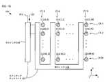
図1Aおよび図1Bは、本開示によるビーム誘導システムの例示的な実施形態の側面および上面の概略図を示す。ビーム誘導システム100は、レンズ102と、プログラマブルカプラ配列104と、コントローラ106とを含む。システム100は、入力光信号120を受信し、その光エネルギーを自由空間出力ビーム108としてコリメートして、出力ビームを3次元ボリュームを通して誘導するように構成される。図示の例では、光信号120は連続波(CW)信号であるが、システム100は、事実上任意の光信号(たとえば、周波数変調連続波(FMCW)信号、LiDAR信号、光パルスなど)に対して作動する。 1A and 1B show schematic side and top views of an exemplary embodiment of a beam steering system according to the present disclosure.
レンズ102は、光軸A1と、焦点面FP1を画定する焦点距離fとを有する、単一の凸凸屈折レンズである。いくつかの実施形態では、レンズ102は、複合レンズ(たとえば、テレセントリックレンズなど)、またはたとえば、1つまたは複数の収差を補正するか、もしくは場合によっては光学性能を改善するように構成された他の多素子レンズなど、異なるタイプのレンズである。いくつかの実施形態では、レンズ102は、平凸レンズである。いくつかの実施形態では、レンズ102は、一般的に低コストであってモバイルシステムを可能にし得る携帯電話レンズである。いくつかの実施形態では、レンズ102は、回折レンズ、ホログラフィック素子、メタサーフェスレンズなどの回折素子である。 Lens 102 is a single convex-convex refractive lens having an optical axis A1 and a focal length f defining a focal plane FP1. In some embodiments, lens 102 is a compound lens (eg, a telecentric lens, etc.) or other lenses configured, for example, to correct one or more aberrations, or possibly improve optical performance. different types of lenses, such as multi-element lenses. In some embodiments, lens 102 is a plano-convex lens. In some embodiments, lens 102 is a cell phone lens that is typically low cost and may enable mobile systems. In some embodiments, lens 102 is a diffractive element, such as a diffractive lens, holographic element, metasurface lens, or the like.
プログラマブルカプラ配列104(以後、カプラ配列104と呼ぶ)は、スイッチングネットワーク110と、垂直カプラ112(1,1)~112(M,N)(カプラ112と総称する)とを含む。垂直カプラ112は、カプラ行CR-1~CR-M(カプラ行CRと総称する)とカプラ列CC-1~CC-N(カプラ列CCと総称する)とを含む2次元配列として配列される。 Programmable coupler array 104 (hereafter referred to as coupler array 104) includes switching network 110 and vertical couplers 112(1,1) through 112(M,N) (collectively couplers 112). The
図示の例では、スイッチングネットワーク110およびカプラ112は、基板114上にモノリシックに集積されるが、いくつかの実施形態では、プログラマブルカプラ配列104の1つまたは複数の要素は、バンプボンディング、マルチチップモジュールパッケージングなど、異なる集積方法を使用して基板114上に配置される。 In the illustrated example, switching network 110 and
図示の例では、基板114はシリコン基板である。シリコン基板の使用は、カプラ配列104の能力を増大することができる集積回路および/または他の回路の容易な包含を可能にする。いくつかの実施形態では、そのようなオンチップ能力は、信号変調、位相シフト、光検知器、処理、メモリ、信号調整、前置増幅、エネルギースカベンジングおよび/または貯蔵などのための電子機器を含む。いくつかの実施形態では、LiDARシステムのすべての電子機器機能は、基板114上にモノリシックに集積される。 In the illustrated example, substrate 114 is a silicon substrate. The use of a silicon substrate allows easy inclusion of integrated circuits and/or other circuits that can increase the capabilities of
コントローラ106は、高精度の多軸位置決めシステム、ボイスコイル、圧電アクチュエータ、MEMSアクチュエータなどの位置決めシステムを介してx次元、y次元およびz次元の各々の中でレンズ102およびカプラ配列104の位置を制御するように構成された従来型コントローラである。コントローラ106は、スイッチングネットワーク110の状態を、それゆえカプラ配列のうちのどの1つまたは複数のカプラが励起されるかを制御するためにも作動する。いくつかの実施形態では、コントローラ106は、少なくとも部分的にカプラ配列104上に集積される。 Controller 106 controls the position of lens 102 and
本開示は、ビーム誘導用途に向けられるが、本明細書で開示する教示はまた、誘導可能レシーバ(すなわち、受信する方向が制御可能なレシーバ)だけでなく、ビーム誘導トランスミッタと誘導可能レシーバの両方を含むトランシーバにも適用可能であることに留意されたい。 Although the present disclosure is directed to beam steering applications, the teachings disclosed herein are also applicable to both beam steering transmitters and steerable receivers, as well as steerable receivers (i.e., receivers whose direction of reception is controllable). Note that it is also applicable to transceivers containing
図示の例では、レンズ102およびカプラ配列104は、それらが同心であり、それらの間の間隔s1がレンズ102の焦点距離fに等しくなるように配列される。その結果、カプラ112の平面は、実質的に焦点面FP1に配置され、光軸A1は、カプラ112の配列上に中心が置かれ、それにより、中心点CP1を画定する。いくつかの実施形態では、レンズ102は、レンズおよびカプラ配列が、レンズの焦点距離以外の距離によって分離されるように、および/または光軸A1の中心がカプラ配列のカプラ112の配列上に置かれないように配置される。 In the illustrated example, lens 102 and
図示の例では、コントローラ106は、随意に、レンズ102およびカプラ配列104の、x次元およびy次元の各々における横調整を制御するために、スキャン方向SD1に沿ってレンズ102をスキャンするように構成される。そのような横スキャニング能力は、出力ビーム108が、カプラ配列の中の各カプラの固定位置によって指示される角度の間を円滑に動かされ、それにより固定位置システムによって可能な数より多数の解像可能な点を実現することを可能にする。いくつかの実施形態では、コントローラ106は、レンズとカプラ配列との間の垂直間隔s1を制御し、それにより、出力ビーム108が空間の中の異なる点において集束することを可能にするようにさらに構成される。レンズとカプラ配列との間の横調整は、レンズ102のみ、カプラ配列104のみを動かすことによって、またはレンズとカプラ配列の両方を動かすことによって制御され得ることに留意されたい。 In the illustrated example, controller 106 is optionally configured to scan lens 102 along scan direction SD1 to control lateral adjustment of lens 102 and
スイッチングネットワーク110は、行スイッチ116と列スイッチ118とを含み、それらは、プログラマブルカプラ配列全体を通して光信号120の光エネルギーの分配を全体的に制御する。図示の例では、スイッチングネットワーク110は、光信号120の光エネルギーのすべを1つだけのカプラ112に案内するように構成される。スイッチングネットワーク110は、図2に関して以下でより詳細に説明する。 Switching network 110 includes row switches 116 and column switches 118, which generally control the distribution of optical energy of
カプラ112(i,j)、ここでi=1~Mおよびj=1~N、の各々は、カプラ配列104の中の集積された光学的導波路(すなわち、カプラ導波路)の構造の中に集積され、その出力光信号120’が、そのそれぞれのカプラとレンズ102の中心との間の幾何学的な線と実質的に整列された出力軸A2で特徴づけられるように構成された回折格子を含む。いくつかの実施形態では、カプラ112の少なくとも1つの回折格子が、高効率を達成するためにブレーズド回折格子であることが好ましい。加えて、図示の例では、カプラ112の各々は、光信号120’の各々が、レンズ102の開口部を実質的に満たすような大きい分散角によって特徴づけられる。各カプラ112の設計は、一般的に、カプラ配列104を有するその位置に基づくことに留意されたい。 Each of the couplers 112(i,j), where i=1-M and j=1-N, is in the structure of integrated optical waveguides (ie, coupler waveguides) in the
光軸A2とレンズ102の中心との調整によって、光信号120’は、レンズの開口部のより大きい部分を照明し、そのことが、遠視野における出力ビーム108の発散角を軽減し、出力ビーム108がその分解能で誘導され得る分解能を高める。 Due to the alignment of the optical axis A2 with the center of the lens 102, the optical signal 120' illuminates a larger portion of the aperture of the lens, which reduces the divergence angle of the
各カプラ112(i,j)は、それが、オン状態とオフ状態との間で切り替えられ得るように構成される。そのオン状態では、カプラ112(i,j)は、その格子構造が光信号120を受信し、その光エネルギーを光信号120’(i,j)として自由空間に散乱させるように、入力ポートIP1と光学的に結合される。そのオフ状態では、カプラ112(i,j)は、入力ポートIP1から光学的に切り離され、その格子構造は、光信号120を受信しない。好ましくは、各カプラ112は、レンズ102の収差を補正するように設計される。カプラ112の格子素子に対する多くの異なる設計は、1次元格子または2次元格子を含めて、本発明の範囲の中に入ることに留意されたい。 Each coupler 112(i,j) is configured such that it can be switched between an on state and an off state. In its on state, coupler 112(i,j) is coupled to input port IP1 such that its lattice structure receives
レンズ102は、カプラ配列104の中の信号112(i,j)の位置に依存する光軸A1からの距離において光信号120’(i、j)を受信する。その結果、異なる垂直カプラによって放射されたすべての光信号がコリメートされ、レンズ102によって異なる出力軸A2(i、j)に沿って誘導される。 Lens 102 receives
図1C~図1Dは、異なるビーム誘導状態における、本開示による、例示的ビーム誘導システムの概略斜視図を示す。ビーム誘導システム100Aは、プログラマブルカプラ配列104が、3x3配列に配列された9つだけのカプラ112A(すなわち、カプラ112A(1,1)~112A(3,3))を含むビーム誘導システム100の一例である。さらに、図1C~図1Dでは、カプラ112A(1,1)~112A(3,3)の各々は、図7に関して以下で説明するように、カプラ配列104の平面に実質的に垂直である伝搬方向に沿って伝搬する比較的より狭い光信号を実現する放射パターンを有する代替カプラ、すなわち具体的には、従来型の垂直格子カプラ、の一例であることに留意されたい。 1C-1D show schematic perspective views of an exemplary beam steering system according to the present disclosure in different beam steering states.
図1Cは、カプラ112(1,1)だけがそのオン状態にあるビーム誘導状態にあるシステム100Aを示す。その結果、カプラ112(1,1)は光信号120を受信し、それを光信号120’(1,1)として自由空間に放出する。レンズ102は、光信号120’(1,1)を受信し、それをコリメートし、出力ビーム108(1,1)として出力軸A2(1,1)に沿って案内する。出力ビーム108(1,1)は、角度θx1およびθy1に向けられる出力軸A2(1,1)に沿って伝搬する。角度θx1およびθy1は、光軸A1に対する、それぞれx-z平面およびy-z平面の中の角度である。角度θx1およびθy1は、式:θx=-tan-1(x/f)およびθy=-tan-1(y/f)によって与えられ、ここで、fはレンズ102の焦点面であり、(x,y)は、中心点CP1に対するx-y平面(すなわち、垂直カプラ配列の焦点面)の中の励起された格子カプラの座標である。 FIG. 1C shows
図1Dは、カプラ112(3,3)だけがそのオン状態にあるビーム誘導状態にあるシステム100Aを示す。その結果、カプラ112(3,3)は光信号120を受信し、それを光信号120’(3,3)として自由空間に放出する。レンズ102は、光信号120’(3,3)を受信し、それをコリメートし、出力ビーム108(3,3)として出力軸A2(3,3)に沿って案内する。出力ビーム108(3,3)は、角度θx2およびθy2に向けられる出力軸A2(3,3)に沿って伝搬する。 FIG. 1D shows
図2は、例示的実施形態による、カプラ配列の概略動作図を示す。カプラ配列104は、スイッチングネットワーク110、カプラ112、バス導波路202、および行導波路204-1~204-Mを含む。 FIG. 2 shows a schematic operational diagram of a coupler arrangement, according to an exemplary embodiment.
図2に示すように、カプラ配列104は、MEMS光スイッチ206-1および列スイッチ配列208-1がそれぞれ、それらのオン状態にある一方で、すべての他のMEMS光スイッチ206および列スイッチ配列208が、それらのオフ状態にある、例示的スイッチ構成である(以下で説明する)。その結果、光信号120は、MEMS光スイッチ206-1によってバス導波路202から行導波路204-1に、次いで、列スイッチ配列208-1によって行導波路204-1からカプラ112(1,1)に方向転換される。 As shown in FIG. 2,
バス導波路202および行導波路204-1~204-M(行導波路204と総称する)の各々は、単一結晶シリコンのコアを有する単一モードのリッジ導波路である。図示の例では、バス導波路および行導波路は、同一平面上にある。いくつかの実施形態では、バス導波路および行導波路のうちの少なくとも1つは、マルチモードの導波路である。いくつかのそのような実施形態では、マルチモードの導波路は、大きい幅を含み、光学的損失を低減するべくその基本モードが励起され得るように構成される。 Each of
図示の例は、シリコンベースのリッジ導波路であるバス導波路および行導波路(および以下で説明するシャント導波路および結合導波路)を含むが、いくつかの実施形態では、異なる導波路構造(たとえば、リブ導波路など)および/または異なる導波路材料のシステムが、少なくとも1つの導波路のために使用される。たとえば、窒化シリコンコア導波路などの誘電体ベースの導波路の使用では、より低い光学的損失および/または増大された光出力処理能力(ピークまたは平均)を有するシステムを実現することができ、それは、非線形効果などを軽減することができる。 Although illustrated examples include silicon-based ridge waveguides, bus waveguides and row waveguides (and shunt waveguides and coupling waveguides discussed below), in some embodiments different waveguide structures ( For example, rib waveguides, etc.) and/or systems of different waveguide materials are used for at least one waveguide. For example, the use of dielectric-based waveguides, such as silicon nitride core waveguides, can provide systems with lower optical losses and/or increased optical power handling capability (peak or average), which , non-linear effects, etc. can be mitigated.
スイッチングネットワーク110は、行スイッチ116および列スイッチ118を含む。 Switching network 110 includes row switches 116 and column switches 118 .
行スイッチ116は、MEMS光スイッチ206-1~206-M(MEMS光スイッチ206と総称する)を含む1xM個のスイッチであり、それは、バス導波路202と行導波路204-1~204-Mそれぞれとの間の光結合を制御するための、別々に制御可能な1x2個の集積された光学ベースのMEMSスイッチである。
図3Aは、MEMS光スイッチ206の概略上面図を示す。 FIG. 3A shows a schematic top view of MEMS
図3B~図3Cは、それぞれ、その「オフ」状態およびオン状態にある代表的MEMS光スイッチ206の概略斜視図を示す。 3B-3C show schematic perspective views of a representative MEMS
MEMS光スイッチ206は、バス導波路202の一部、行導波路204の一部、シャント導波路302、およびMEMSアクチュエータ304(図3B~図3Cに示さず)を含む。 MEMS
図示の例では、バス導波路202および行導波路204の一部は、それらの間で導波路が交差しないように配列される。その結果、非常に低い光学的挿入損失だけでなく、実質的にゼロの導波路間の光学的クロストークも達成することができる。しかしながら、いくつかの実施形態では、2つの導波路の部分は、好ましくは、それらが直交して、MEMS光スイッチ206がそのオフ状態にあるときにバス導波路202の行導波路204への漏洩を軽減するように、交差点において交差する。いくつかの実施形態では、バス導波路202は、マルチモード干渉(MMI)領域と、MMI領域の中に至りその外に出るテーパとを含む。いくつかの実施形態では、バス導波路202および行導波路204は、それらの共通基板の上の異なる平面の中に形成される。 In the illustrated example, portions of
シャント導波路302は、端部306-1と306-2との間に延びる導波路部である。シャント導波路302は、バス導波路202および行導波路204に類似するが、シャント導波路302は、バス導波路および行導波路に対して可動であるように構成される。
端部306-1および306-2(端部306と総称する)は、導波路部308-1および308-2それぞれの真上に整列され、ここで導波路部308-1および308-2(導波路部308と総称する)は、バス導波路202および行導波路204それぞれの一部である。 Edges 306-1 and 306-2 (collectively edge 306) are aligned directly above waveguide sections 308-1 and 308-2, respectively, where waveguide sections 308-1 and 308-2 ( Waveguide sections 308) are portions of
図3A~図3Cに明確には示されないが、一般的に、シャント導波路302は、MEMS光スイッチ206がオン状態にあるときに端部306と導波路部308との間に正確な垂直間隔を確立するためにその下面から延びる突出部も含む。 Although not explicitly shown in FIGS. 3A-3C, generally the
MEMSアクチュエータ304は、導波路部308-1および308-2に対するシャント導波路302および端部306の垂直位置を制御するために作動する静電MEMS垂直アクチュエータである。MEMSアクチュエータ304は、図4A~図4Cに関して以下でより詳細に説明する。 MEMS actuator 304 is an electrostatic MEMS vertical actuator that operates to control the vertical position of
MEMS光スイッチ206は、図示の実施形態では静電MEMS垂直アクチュエータを含むが、当業者には、本明細書を読めば、端部306と導波路部308との間の間隔を制御するために好適な任意のアクチュエータを、いかにして規定し、作製し、かつ使用するかが明らかとなろう。本発明における使用に好適なアクチュエータには、限定はしないが、垂直アクチュエータ、横アクチュエータ、および垂直と横の両方に作動するアクチュエータが含まれる。さらに、本発明によるアクチュエータには、限定はしないが、電熱、熱、磁気、電磁、静電コームドライブ、磁歪、圧電、流体、空気圧のアクチュエータなどを含む。 MEMS
MEMS光スイッチ206がその切り替えられていない(すなわち「オフ」)状態にあるとき、シャント導波路302は、端部306-1および306-2が導波路部308-1と308-2から距離d1だけ離隔される第1の位置に保持される。距離d1は、光エネルギーが、端部306とそれらのそれぞれの導波路部との間で実質的に転移しないことを確実にするのに十分な大きさを有する。その結果、光信号120はMEMS光スイッチ206をバイパスし、実質的に摂動することなくバス導波路202を通って伝搬することを継続する。 When MEMS
MEMS光スイッチ206がその切り替えられた(すなわち「オン」)状態にあるとき、シャント導波路302は、端部306が導波路部308から距離d2だけ離隔され、それにより指向性カプラ310-1および310-2を画定する、第2の位置に移される。距離d2は、シャント導波路の底の突出部の高さによって決定され、光信号120の光エネルギーが、指向性カプラ310-1において導波路部308-1から端部306-1に、および指向性カプラ310-2において端部306-2から導波路部308-2に実質的に完全に転移することを可能にする大きさを有する。その結果、光信号120は、バス導波路202から行導波路204に実質的に完全に切り替えられる。 When MEMS
MEMS光スイッチ206は、集積された光学ベースのMEMS光スイッチの一例にすぎないことに留意されたい。本開示の教示による使用に好適なMEMSスイッチの追加の例は、T. J. Seokら、「Large-scale broadband digital silicon photonic switches with vertical adiabatic couplers」、Optica、vol. 3、no. 1、64ページ、2016年1月、ならびに米国特許出願第20160327751号、および国際出願第WO2018/049345号によって記載されており、それらの各々は、参照により本明細書に組み込まれる。これらの出版物に記載されるそのようなMEMSスイッチは、従来技術のビーム誘導システムに対して、本開示によるプログラマブルカプラ配列に対する多くの利点を提示する。特に、そのようなスイッチは、従来の電気光学または熱光学のスイッチよりかなり低い光学的損失を有し、それらの光学的クロストーク(-60dB未満)および電力消費(10マイクロワットまで)は、従来のスイッチより数桁低く、それらはデジタルモードで動作することができる。これらの利点は、従来技術で可能なものより比較的高いスループット(すなわち、より低い光学的挿入損失)および比較的高い分解能(すなわち、より高密度の格子カプラ)ならびに単純なデジタル制御を有するビーム誘導デバイスを可能にする。 Note that MEMS
ここで図2に戻ると、列スイッチ118は、列スイッチ配列208-1~208-N(列スイッチ配列208と総称する)を含む1xN個のスイッチである。 Returning now to FIG. 2, column switch 118 is a 1×N number of switches including column switch arrays 208-1 through 208-N (collectively column switch array 208).
図示の例では、各列スイッチ配列208は、M個の実質的に同一のMEMS光スイッチ210を含み、それらの各々はMEMS光スイッチ206に類似するが、各MEMS光スイッチ210は、それぞれのカプラ112と行導波路204との間の光結合を制御するように構成される。各MEMS光スイッチ210およびその関連するカプラ112は、MEMS制御垂直カプラ212を全体的に画定する。 In the illustrated example, each
図示の例では、各列スイッチ配列208のMEMS光スイッチ210のすべては、それらが同じ制御信号ですべて制御されるように「連動」される(ganged together)。その結果、各列スイッチ配列208は、カプラ配列104のそのそれぞれの列におけるすべてのM個のカプラ112とそれらのそれぞれの行導波路との間の光結合を同時に制御する。そのようなスイッチ配列構成は、多数のカプラ(たとえば、MおよびNの各々が1000以上であるMxN配列)を有し、各カプラが個々にアドレス指定される場合にはMxN個の制御信号が必要である、ビーム誘導システムに対して特に有利である。大規模システムに対して、電気入力/出力(I/O)の数は、標準的な電気パッケージング限界をすぐに超える。しかしながら、列スイッチ配列208などのスイッチ配列の使用では、制御信号の数をMxNからM+Nに低減する「行-列」アドレス指定方式を可能にすることによって、必要な電気的制御信号の数を顕著に低減することができる。 In the illustrated example, all of the MEMS
各MEMS制御垂直カプラ212のオン状態では、そのMEMS光スイッチ210は、そのそれぞれの行導波路204をそのそれぞれのカプラ112と光学的に結合する。その結果、光信号120が、その行導波路を通って伝搬しているとき、その光エネルギーは、そのカプラ112に方向転換される。各MEMS制御垂直カプラ212のオフ状態では、そのMEMS光スイッチ210は、そのそれぞれの行導波路とカプラとを光学的に結合せず、それゆえ、光信号120は、行導波路の中に留まって、そのカプラをバイパスする。 In the ON state of each MEMS-controlled
図4Aは、例示的実施形態による、例示的MEMS制御垂直カプラの概略上面図を示す。MEMS制御垂直カプラ212は、MEMS光スイッチ210とカプラ112とを含む。 FIG. 4A shows a schematic top view of an exemplary MEMS-controlled vertical coupler, according to an exemplary embodiment. MEMS-controlled
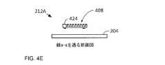
図4B~図4Cは、それぞれ、その「オフ」状態およびオン状態にあるMEMS制御垂直カプラ212の概略断面図を示す。図4B~図4Cに示す断面図は、図4Aに示す線a-aを通して取られる。 4B-4C show schematic cross-sectional views of MEMS-controlled
MEMS光スイッチ210は、MEMSアクチュエータ404と動作可能に結合されたカプラ導波路402の一部を含む。 MEMS
カプラ導波路402は、シャント導波路302に類似し、可動端部406-1から固定端部406-2に光を搬送するように構成され、固定端部406-2において、垂直結合要素408が配置され、それによりカプラ112が画定される。図示の例では、垂直結合要素408は、光軸A1が中心点CP1と整列されているとき、その光エネルギーをレンズ102の中心の方に案内するように構成された回折格子である。いくつかの実施形態では、垂直結合要素408のうちの少なくとも1つは、所望の出力光信号120’を供給するのに好適な異なる光学素子を含む。垂直結合要素408における使用に好適な光学素子は、限定はしないが、プリズム、ホログラム、2次元格子構造、回折レンズ、回折格子素子、屈折レンズ、角度エッチング導波路ファセットミラー、角度エッチング導波路、角度付きミラーなどを含む。
可動端部406-1において、カプラ導波路402は、MEMSアクチュエータ404に取り付けられる。 At movable end 406 - 1 ,
固定端部406-2において、カプラ導波路402は、下部の基板114から上に突き出る硬い要素であるアンカー410のペアに物理的に取り付けられる。カプラ導波路は、この領域の中の硬い構造要素に添付されるので、行導波路204の上のその高さは固定される。 At fixed end 406 - 2 ,
MEMSアクチュエータ404は、上記で説明したMEMSアクチュエータ304に類似し、アンカー410の別のペアに接続される支柱412、電極414およびテザー416を含む。 MEMS actuator 404 is similar to MEMS actuator 304 described above and includes struts 412 , electrodes 414 and tethers 416 connected to another pair of
支柱412は、可動端部406-1を電極414の各々に接続する実質的に硬い要素である。 Posts 412 are substantially rigid elements that connect movable ends 406 - 1 to each of electrodes 414 .
電極414は、電極の2つのペアの間に印加された電圧が、電極、支柱および可動端部を基板の方に引っ張る静電力を生じ、それにより、カプラ導波路402と行導波路204との間の間隔が低減されるように、基板114(図示せず)上に配置された電極のマッチングペアの上に配置される。 Electrodes 414 are configured such that a voltage applied between the two pairs of electrodes creates an electrostatic force that pulls the electrodes, posts and movable ends toward the substrate, thereby connecting
テザー416は、z方向に柔軟であるがx方向およびy方向に沿って実質的に硬い「ばねのような」要素である。テザー416の柔軟性は、行導波路204に対する可動端部406-1の運動を可能にする。 Tether 416 is a “spring-like” element that is flexible in the z-direction but substantially stiff along the x- and y-directions. The flexibility of tether 416 allows movement of movable end 406 - 1 relative to row
MEMSアクチュエータ404が、その非作動状態にあるとき、可動端部406-1は、行導波路204から距離d1だけ離隔される。その結果、2つの導波路は、上記で説明したように、光学的に結合されず、カプラ112はそのオフ状態にある。 When MEMS actuator 404 is in its unactuated state, movable end 406-1 is separated from
MEMSアクチュエータ404がその作動状態にあるとき、可動端部406-1は、それが、突出部418の高さによって決定される距離d2だけ行導波路204から離隔されることになるように、下方に引き下げる。その結果、2つの導波路は、実質的にすべての光信号120がカプラ導波路402にエバネッセント結合して、格子素子408に伝搬することを可能にする指向性カプラ420を全体的に画定する。次いで、光信号の光エネルギーは、格子素子408によって自由空間に放出され、カプラ112はそのオン状態にある。 When MEMS actuator 404 is in its actuated state, movable end 406-1 is downwardly tilted such that it is separated from
MEMS制御垂直カプラ212は例にすぎず、MEMS制御垂直カプラ212に対する無数の代替設計は、本開示の範囲内に入ることに留意されたい。 Note that the MEMS-controlled
たとえば、いくつかの実施形態では、カプラ導波路は、MEMS制御垂直カプラ212の中に含まれず、格子素子は、MEMSアクチュエータ404自体の上に配置される。 For example, in some embodiments, coupler waveguides are not included in MEMS-controlled
図4Dは、本開示による、MEMS制御垂直カプラの代替実施形態の概略上面図を示す。MEMS制御垂直カプラ212Aは、MEMSアクチュエータ404、格子素子408、プラットフォーム422、およびカプラ導波路424を含む。 FIG. 4D shows a schematic top view of an alternate embodiment of a MEMS-controlled vertical coupler according to the present disclosure; MEMS-controlled
プラットフォーム422は、MEMSアクチュエータの中心に形成された実質的に硬い構造要素である。プラットフォーム422は、カプラ導波路402の可動部分に類似するカプラ導波路424を含む。 Platform 422 is a substantially rigid structural element formed at the center of the MEMS actuator. Platform 422 includes a
図4E~図4Fは、それぞれ、そのオフ状態およびオン状態にあるMEMS制御垂直カプラ212Aの概略図を示す。図4E~図4Fに示す断面図は、図4Dに示す線b-bを通して取られる。 4E-4F show schematic diagrams of MEMS-controlled
MEMSアクチュエータ404が、その非作動状態にあるとき、可動端部406-1は、行導波路204から距離d1だけ離隔される。その結果、2つの導波路は光学的に結合されず、カプラ112はオフ状態にある。 When MEMS actuator 404 is in its unactuated state, movable end 406-1 is separated from
MEMSアクチュエータ404がその作動状態にあるとき、行導波路204およびカプラ導波路424は指向性カプラ426を全体的に画定し、指向性カプラ426は、光エネルギーを行導波路から直接格子素子408に結合し、格子素子408は、次いで、エネルギーを自由空間に放射する。 When MEMS actuator 404 is in its actuated state,
いくつかの実施形態では、MEMS制御垂直カプラ212は、同じ平面内にある行導波路と結合導波路とを含み、スイッチングは、上記で説明したように、可動シャント導波路を使用して実現される。 In some embodiments, the MEMS-controlled
図4Gは、本開示による、別の代替のMEMS制御垂直カプラの概略上面図を示す。MEMS制御垂直カプラ212Bは、MEMSアクチュエータ304、行導波路204、カプラ導波路424、シャント導波路302、およびカプラ112を含む。MEMS制御垂直カプラ212Bは、図3A~図3Cに関して上記で説明したMEMS光スイッチ206に類似する。 FIG. 4G shows a schematic top view of another alternative MEMS controlled vertical coupler according to the present disclosure. MEMS-controlled
MEMSアクチュエータ304がその非作動状態にあるとき、シャント導波路は、行導波路204およびカプラ導波路424の十分上に保持される。その結果、2つの導波路は光学的に結合されず、カプラ112は励起されない。 The shunt waveguide is held well above the
MEMSアクチュエータ304がその作動状態にあるとき、シャント導波路302は、行導波路204およびカプラ導波路424の各々と光学的に結合され、それにより、指向性カプラをシャント導波路の各端部において画定する。その結果、光エネルギーは、行導波路からシャント導波路に、次いで、シャント導波路から結合導波路に結合する。光エネルギーは、結合導波路によってカプラ112に搬送され、それにより、カプラ112が光エネルギーを自由空間に放射するようにカプラ112を励起する。 When the MEMS actuator 304 is in its actuated state, the
図5は、本開示による、代替プログラマブルカプラ配列を示す。カプラ配列500は、カプラ配列104に類似するが、カプラ配列500は、複数の光信号を複数のカプラ112に案内し、それにより、複数の出力ビームを同時に形成して誘導することができるビーム誘導システムを可能にするように構成される。 FIG. 5 shows an alternative programmable coupler arrangement according to the present disclosure.
カプラ配列500は、スイッチングネットワーク502、垂直カプラ112、バス導波路202、および行導波路204-1~204-Mを含む。
スイッチングネットワーク502は、行スイッチ504および列スイッチ506-1~506-Mを含む。 Switching network 502 includes row switch 504 and column switches 506-1 through 506-M.
行スイッチ504は、入力信号120-1~120-Lのいずれかを行導波路204-1~204-Mのうちの異なる1つに案内するように作動するLxM個のスイッチである。 Row switches 504 are L×M switches that operate to direct any of input signals 120-1 through 120-L to different ones of row waveguides 204-1 through 204-M.
列スイッチ506-1~506-Mの各々は、N個のスイッチ510を含む1xN個の光スイッチである。列スイッチ506-1は、行スイッチ504から受信する光信号をカプラ112(1,1)~112(1,N)のうちの1つに案内し、列スイッチ506-2は、光信号120-2をカプラ112(2,1)~112(2,N)のうちの1つに案内し、以下同様である。 Each of column switches 506 - 1 through 506 -M is a 1×N optical switch including N switches 510 . Column switch 506-1 directs optical signals received from row switch 504 to one of couplers 112(1,1) through 112(1,N), and column switch 506-2 directs optical signals 120- 2 to one of couplers 112(2,1) through 112(2,N), and so on.
その結果、カプラ配列500を含むビーム誘導システムは、複数の個別に誘導可能なコリメートされた出力ビーム110-1~110-Lを供給することができる。 As a result, a beam steering system including
上記で説明したように、必要な電気信号の数は、個別に制御可能なスイッチを有するビームシステムに対して問題となることがある。たとえば、システム500では、必要な電気信号の数は、NxM+LxMである。しかしながら、いくつかの実施形態では、集積された電気アドレス指定回路が、電気パッケージング問題を軽減するために含まれる。そのような集積は、モノリシック集積、ハイブリッド集積、フリップチップボンディングなど、広く知られている技法のいずれかを介して達成され得る。 As explained above, the number of electrical signals required can be an issue for beam systems with individually controllable switches. For example, in
システム500のアーキテクチャは、行ごとに1つだけのカプラ112が、行スイッチ504から光信号を受信することができるという意味でブロッキングであることに留意されたい。 Note that the architecture of
図6は、本開示による、別の代替プログラマブルカプラ配列を示す。プログラマブルカプラ配列600は、複数の個別に誘導可能な出力ビームを供給するように構成されたビーム誘導システムにおいて使用するのに好適な非ブロッキングカプラ配列である。プログラマブルカプラ配列600は、プログラマブルカプラ配列500に類似するが、スイッチングネットワーク602は、LxM個の光スイッチである1つの行スイッチと、PxN個の光スイッチであるM個の列スイッチとを含む。 FIG. 6 shows another alternative programmable coupler arrangement according to the present disclosure.
カプラ配列600は、スイッチングネットワーク602、垂直カプラ112、バス導波路202、および行導波路204-1~204-MxPを含む。
スイッチングネットワーク602は、行スイッチ604および列スイッチ606-1~606-Mを含む。 Switching network 602 includes row switch 604 and column switches 606-1 through 606-M.
行スイッチ604は、入力信号120-1~120-Lのいずれかをバス導波路204-1~204-MxPのうちの異なる1つに案内するために作動するLx(MxP)個のスイッチである。 Row switches 604 are Lx (MxP) switches that operate to direct any of input signals 120-1 through 120-L to different ones of bus waveguides 204-1 through 204-MxP. .
列スイッチ506-1~506-Mの各々は、P個の行導波路204の各々の上で受信された光信号をN個のカプラ112のいずれかに案内することができるPxN個の光スイッチである。列スイッチ606-1は、行導波路204(1,1)~204(1,P)の各々の上で受信する光信号をカプラ112(1,1)~112(1,N)のうちのいずれか1つに案内し、列スイッチ606-2は、行導波路204(2,1)~204(2,P)の各々の上で受信する光信号をカプラ112(2,1)~112(2,N)のうちの1つに案内し、以下同様である。 Each of the column switches 506-1 through 506-M is a P×N optical switch capable of directing the optical signal received on each of the
言い換えれば、カプラ112の各行は、P個の導波路およびPxN個のスイッチ606を通してLx(MxP)個のスイッチ604に接続される。その結果、P個の入力信号のいずれも、同じ行の中の格子カプラに同時にアクセスすることができる。 In other words, each row of
図7は、本開示による、代替ビーム誘導システムの概略側面図を示す。ビーム誘導システム700は、ビーム誘導システム100に類似するが、ビーム誘導システム700は、従来の垂直格子カプラであるカプラを含むカプラ配列702を含む。 FIG. 7 shows a schematic side view of an alternative beam steering system according to the present disclosure;
カプラ配列702は、スイッチングネットワーク110と、垂直カプラ704(1,1)~704(M,N)(カプラ704と総称する)とを含む。 Coupler array 702 includes switching network 110 and vertical couplers 704(1,1) through 704(M,N) (collectively couplers 704).
カプラ704は、カプラ112に類似するが、図示の例では、カプラ704は、焦点面FP1に実質的に垂直である伝搬方向に沿って伝搬する比較的小発散角の(small-divergence)光信号としてそれらの自由空間放射(すなわち、光信号706)を直接供給するように構成された、従来の垂直格子カプラである。その結果、光信号706は、レンズ102の開口部の比較的小さい部分とだけ相互作用する。 Coupler 704 is similar to
レンズ102は光信号706を受信し、それを出力ビーム708としてコリメートし、それが光軸A3に沿って伝搬するように出力ビームを方向転換させる。図1A~図1Dに関して上記で説明したように、光軸A1に対する出力軸A3の角度は、カプラ配列702の中のカプラ704(i、j)の位置に依存する。 Lens 102 receives
本開示は、例示的実施形態の一例だけを教示しており、本発明の多くの変形形態は、この開示を読んだ後の当業者によって容易に考案され得、本発明の範囲は、以下の特許請求の範囲によって決定されるべきであることを理解されたい。 The present disclosure teaches only one example of an exemplary embodiment, and many variations of the invention can be readily devised by those of ordinary skill in the art after reading this disclosure, and the scope of the invention is the following: It should be understood that the scope of the claims should be determined.
100 ビーム誘導システム
100A ビーム誘導システム
102 レンズ
104 プログラマブル垂直カプラ配列
106 コントローラ
108 出力ビーム
108(1,1) 出力ビーム
108(3,3) 出力ビーム
110 スイッチングネットワーク
112 カプラ
112(1,1) カプラ
112(1,2) カプラ
112(1,N) カプラ
112(2,1) カプラ
112(2,2) カプラ
112(2,N) カプラ
112(M,1) カプラ
112(M,2) カプラ
112(M,N) カプラ
112(i,j) カプラ
112A カプラ
112A(1,1) カプラ
112A(2,2) カプラ
112A(3,3) カプラ
114 基板
116 行スイッチ
118 列スイッチ
120 光信号
120’ 光信号
120-1 光信号
120-L 光信号
120’(1,1) 光信号
120’(3,3) 光信号
120’(i,j) 光信号
202 バス導波路
202-1 バス導波路
202-L バス導波路
204 行導波路
204-1 行導波路
204-2 行導波路
204-M 行導波路
204(1,1) 行導波路
204(1,P) 行導波路
204(M,1) 行導波路
204(M,P) 行導波路
206 MEMS光スイッチ
206-1 MEMS光スイッチ
206-2 MEMS光スイッチ
206-M MEMS光スイッチ
208 列スイッチ配列
208-1 列スイッチ配列
208-2 列スイッチ配列
208-N 列スイッチ配列
210 MEMS光スイッチ
212 MEMS制御垂直カプラ
212A MEMS制御垂直カプラ
212B MEMS制御垂直カプラ
214 スイッチ
302 シャント導波路
304 MEMSアクチュエータ
306 端部
306-1 端部
306-2 端部
308 導波路部
308-1 導波路部
308-2 導波路部
310-1 第1の指向性カプラ
310-2 第2の指向性カプラ
402 カプラ導波路
404 MEMSアクチュエータ
406-1 可動端部
406-2 固定端部
408 垂直結合要素、格子素子
410 アンカー
412 支柱
414 電極
416 テザー
418 突出部
420 指向性カプラ
422 プラットフォーム
424 カプラ導波路
426 指向性カプラ
500 カプラ配列
502 スイッチングネットワーク
504 行スイッチ
506 列スイッチ
506-1 列スイッチ
506-2 列スイッチ
506-M 列スイッチ
600 プログラマブルカプラ配列
604 行スイッチ、スイッチングネットワーク
606 列スイッチ
606-1 列スイッチ
606-2 列スイッチ
606-M 列スイッチ
700 ビーム誘導システム
702 カプラ配列
704 垂直カプラ
704(1,1) 垂直カプラ
704(M,N) 垂直カプラ
706 光信号
708 出力ビーム100 beam steering system 100A beam steering system 102 lens 104 programmable vertical coupler array 106 controller 108 output beam 108(1,1) output beam 108(3,3) output beam 110 switching network 112 coupler 112(1,1) coupler 112( 1,2) Coupler 112(1,N) Coupler 112(2,1) Coupler 112(2,2) Coupler 112(2,N) Coupler 112(M,1) Coupler 112(M,2) Coupler 112(M , N) coupler 112(i,j) coupler 112A coupler 112A(1,1) coupler 112A(2,2) coupler 112A(3,3) coupler 114 substrate 116 row switch 118 column switch 120 optical signal 120' optical signal 120 -1 optical signal 120-L optical signal 120'(1,1) optical signal 120'(3,3) optical signal 120'(i,j) optical signal 202 bus waveguide 202-1 bus waveguide 202-L bus Waveguide 204 Row waveguide 204-1 Row waveguide 204-2 Row waveguide 204-M Row waveguide 204 (1, 1) Row waveguide 204 (1, P) Row waveguide 204 (M, 1) Row waveguide Wave path 204 (M, P) Row waveguide 206 MEMS optical switch 206-1 MEMS optical switch 206-2 MEMS optical switch 206-M MEMS optical switch 208 Column switch array 208-1 Column switch array 208-2 Column switch array 208- N row switch array 210 MEMS optical switch 212 MEMS controlled vertical coupler 212A MEMS controlled vertical coupler 212B MEMS controlled vertical coupler 214 switch 302 shunt waveguide 304 MEMS actuator 306 end 306-1 end 306-2 end 308 waveguide section 308 -1 waveguide section 308-2 waveguide section 310-1 first directional coupler 310-2 second directional coupler 402 coupler waveguide 404 MEMS actuator 406-1 movable end 406-2 fixed end 408 vertical Coupling Elements, Grating Elements 410 Anchors 412 Posts 414 Electrodes 416 Tethers 418 Protrusions 420 Directional Couplers 422 Platforms 424 Coupler Waveguides 426 Fingers Directional Coupler 500 Coupler Array 502 Switching Network 504 Row Switch 506 Column Switch 506-1 Column Switch 506-2 Column Switch 506-M Column Switch 600 Programmable Coupler Array 604 Row Switch, Switching Network 606 Column Switch 606-1 Column Switch 606- 2 row switch 606-M row switch 700 beam steering system 702 coupler array 704 vertical coupler 704(1,1) vertical coupler 704(M,N) vertical coupler 706 optical signal 708 output beam
Claims (23)
Translated fromJapaneseプログラマブル垂直カプラ配列(104)とを含むビーム誘導システム(100)であって、前記プログラマブル垂直カプラ配列(104)が、
基板(114)と、
中心点(CP1)で特徴づけられる2次元配列でありかつ複数のカプラ行(CR)および複数のカプラ列(CC)を有するカプラ(112)の配列であって、カプラの前記配列の各カプラが、カプラ導波路(402)、および前記カプラ導波路から受信された光エネルギーを自由空間に放出するように構成された垂直結合要素(408)を含む、カプラ(112)の配列と、
前記基板上に配置され、第1の光信号(120)を受信するための第1の入力ポート(IP1)を有するバス導波路(202)と、
前記基板上に配置された複数の行導波路(204)と、
前記第1の入力ポートからカプラの前記配列のうちの任意のカプラへの第1の光信号(120)の伝搬を制御するために作動するスイッチングネットワーク(110)とを含み、
前記レンズおよびプログラマブル垂直カプラ配列が、前記レンズが、前記複数の垂直結合要素の各垂直結合要素によって放出された前記光エネルギーを受信し、前記光エネルギーを、前記プログラマブル垂直カプラ配列の中のその垂直結合要素の位置、および前記レンズと少なくとも1つの次元における前記プログラマブル垂直カプラ配列との第1の相対位置に基づく出力軸に案内するように配列される、ビーム誘導システム(100)。a lens (102) having an optical axis (A1) and a focal plane (FP1);
a programmable vertical coupler array (104), said programmable vertical coupler array (104) comprising:
a substrate (114);
An array of couplers (112) being a two-dimensional array characterized by a center point (CP1) and having a plurality of coupler rows (CR) and a plurality of coupler columns (CC), each coupler of said array of couplers having , a coupler waveguide (402), and a vertical coupling element (408) configured to launch optical energy received from said coupler waveguide into free space;
a bus waveguide (202) disposed on the substrate and having a first input port (IP1) for receiving a first optical signal (120);
a plurality of row waveguides (204) disposed on the substrate;
a switching network (110) operable to control propagation of a first optical signal (120) from said first input port to any coupler of said array of couplers;
The lens and programmable vertical coupler array receive the optical energy emitted by each vertical coupling element of the plurality of vertical coupling elements, convert the optical energy to its vertical coupling element in the programmable vertical coupler array, and A beam steering system (100) arranged to guide to an output axis based on a position of a combining element and a first relative position of said lens and said programmable vertical coupler array in at least one dimension.
複数の光信号(120-1~120-L)を前記バス導波路から受信するための複数の入力ポートを含む行スイッチ(504)であって、前記複数の光信号の各光信号を前記複数の行導波路のうちの任意の行導波路に案内するために作動する、行スイッチ(504)と、
複数の列スイッチ(506)とを含み、前記複数の列スイッチの各列スイッチが、前記複数の行導波路のうちの異なる行導波路および前記複数のカプラ行のうちの異なるカプラ行と動作可能に結合され、前記複数の列スイッチの各列スイッチが、そのそれぞれの行導波路と前記複数のカプラ行のうちのそのそれぞれのカプラ行のうちの任意のカプラとの間の光結合を可能にするように構成される、請求項1に記載のシステム。The switching network (504) comprises:
A row switch (504) including a plurality of input ports for receiving a plurality of optical signals (120-1 through 120-L) from said bus waveguides, wherein each optical signal of said plurality of optical signals is connected to said plurality of optical signals. a row switch (504) operable to direct to any of the row waveguides of the
a plurality of column switches (506), each column switch of said plurality of column switches being operable with a different row waveguide of said plurality of row waveguides and a different coupler row of said plurality of coupler rows. and each column switch of said plurality of column switches enables optical coupling between its respective row waveguide and any coupler of its respective coupler row of said plurality of coupler rows. 2. The system of claim 1, configured to:
複数の光信号(120-1~120-L)を前記バス導波路から受信するための複数の入力ポートを含む行スイッチ(604)であって、前記複数の光信号の各光信号を前記複数の行導波路のうちの任意の行導波路に案内するために作動する、行スイッチ(604)と、
複数の列スイッチ(606)とを含み、前記複数の列スイッチの各列スイッチが、第2の複数の導波路(204(1,1)~204(1,P))によって前記行スイッチと動作可能に結合され、前記複数の列スイッチの各列スイッチが、そのそれぞれの第2の複数の行導波路の各々と前記複数のカプラ行のうちのそのそれぞれのカプラ行のうちの任意のカプラとの間の光結合を可能にするように構成され、
前記第1の複数の行導波路が、各第2の複数の行導波路を含む、請求項1に記載のシステム。wherein said switching network (604) is non-blocking, said switching network comprising:
A row switch (604) including a plurality of input ports for receiving a plurality of optical signals (120-1 through 120-L) from said bus waveguides, wherein each optical signal of said plurality of optical signals is connected to said plurality of optical signals. a row switch (604) operable to direct to any of the row waveguides of the
a plurality of column switches (606), each column switch of said plurality of column switches operating with said row switches by means of a second plurality of waveguides (204(1,1)-204(1,P)). operably coupled to each column switch of said plurality of column switches with each of its respective second plurality of row waveguides and any coupler of its respective coupler row of said plurality of coupler rows; configured to allow optical coupling between
2. The system of claim 1, wherein the first plurality of row waveguides comprises a respective second plurality of row waveguides.
前記第1の入力ポートおよび第1の複数のMEMS光スイッチ(206)を含む行スイッチ(116)であって、前記第1の複数のMEMS光スイッチの各MEMS光スイッチが、前記バス導波路と前記複数の行導波路のうちの1つの異なる行導波路とに動作可能に結合され、かつ(1)前記バス導波路がそのそれぞれの行導波路から光学的に切り離される第1の状態と、(2)前記バス導波路およびそのそれぞれの行導波路が光学的に結合される第2の状態とを有する、行スイッチ(116)と、
複数の列スイッチ配列(208)を含む列スイッチ(118)とを含み、前記複数の列スイッチ配列の各列スイッチ配列が、第2の複数のMEMS光スイッチ(210)を含み、前記第2の複数のMEMS光スイッチの各MEMS光スイッチが、前記複数の行導波路のうちの1つの異なる行導波路およびそのそれぞれのカプラ列のうちの1つの異なるカプラと動作可能に結合され、かつ(1)そのそれぞれの行導波路がそのそれぞれのカプラから光学的に切り離される第1の状態と、(2)そのそれぞれの行導波路およびそのそれぞれのカプラが光学的に結合される第2の状態とを有する、請求項1に記載のシステム。The switching network is
a row switch (116) comprising said first input port and a first plurality of MEMS optical switches (206), each MEMS optical switch of said first plurality of MEMS optical switches being coupled to said bus waveguide; a first state in which the bus waveguide is optically decoupled from its respective row waveguide; (2) a row switch (116) having a second state in which said bus waveguide and its respective row waveguide are optically coupled;
a column switch (118) comprising a plurality of column switch arrangements (208), each column switch arrangement of said plurality of column switch arrangements comprising a second plurality of MEMS optical switches (210); each MEMS optical switch of a plurality of MEMS optical switches is operably coupled to a different row waveguide of the plurality of row waveguides and a different coupler of its respective coupler column; and (1 ) a first state in which its respective row waveguide is optically decoupled from its respective coupler; and (2) a second state in which its respective row waveguide and its respective coupler are optically coupled. 2. The system of claim 1, comprising:
前記基板に対して可動であり、第1の端部(360-1)および第2の端部(306-2)を有するシャント導波路(302)と、
(1)前記バス導波路がそのそれぞれの行導波路から光学的に切り離される第1の位置と、(2)前記バス導波路がそのそれぞれの行導波路と光学的に結合される第2の位置との間で前記シャント導波路を動かすように構成されたMEMSアクチュエータ(304)とを含み、
前記MEMSアクチュエータが前記第2の位置にあるとき、
前記第1の端部および前記バス導波路の第1の導波路部(308-1)が、光エネルギーが前記バス導波路から前記シャント導波路に結合することを可能にする第1の指向性カプラ(310-1)を全体的に画定し、
前記第2の端部およびそのそれぞれの行導波路の第2の導波路部(308-2)が、光エネルギーが前記シャント導波路からそのそれぞれの行導波路に結合することを可能にする第2の指向性カプラ(310-2)を全体的に画定する、請求項6に記載のシステム。each MEMS optical switch of the first plurality of MEMS optical switches;
a shunt waveguide (302) movable relative to the substrate and having a first end (360-1) and a second end (306-2);
(1) a first position where the bus waveguides are optically decoupled from their respective row waveguides; and (2) a second position where the bus waveguides are optically coupled with their respective row waveguides. a MEMS actuator (304) configured to move the shunt waveguide between positions;
when the MEMS actuator is in the second position;
The first end and the first waveguide portion (308-1) of the bus waveguide have a first directivity that allows optical energy to be coupled from the bus waveguide to the shunt waveguide. generally defining a coupler (310-1);
The second waveguide portion (308-2) of the second end and its respective row waveguide allows optical energy to couple from the shunt waveguide to its respective row waveguide. 7. The system of claim 6, which generally defines two directional couplers (310-2).
そのそれぞれのカプラの前記カプラ導波路であって、可動端部(406-1)および前記垂直結合要素を含む固定端部(406-2)を有する、前記カプラ導波路と、
(1)前記カプラ導波路がそのそれぞれの行導波路から光学的に切り離される第1の位置と、(2)前記カプラ導波路がそのそれぞれの行導波路と光学的に結合される第2の位置との間で、前記可動端部を動かすように構成されたMEMSアクチュエータ(404)とを含み、
前記MEMSアクチュエータが前記第2の位置にあるとき、前記可動端部およびそのそれぞれの行導波路が、光エネルギーがそのそれぞれの行導波路から前記カプラ導波路に結合することを可能にする指向性カプラ(420)を全体的に画定する、請求項6に記載のシステム。each MEMS optical switch of the second plurality of MEMS optical switches;
said coupler waveguides of their respective couplers, said coupler waveguides having a movable end (406-1) and a fixed end (406-2) containing said vertical coupling element;
(1) a first position where the coupler waveguides are optically decoupled from their respective row waveguides; and (2) a second position where the coupler waveguides are optically coupled with their respective row waveguides. a MEMS actuator (404) configured to move the movable end between positions;
When the MEMS actuator is in the second position, the movable end and its respective row waveguide are directional to allow optical energy to be coupled from its respective row waveguide to the coupler waveguide. 7. The system of claim 6, generally defining a coupler (420).
そのそれぞれのカプラの前記カプラ導波路(424)であって、前記垂直結合要素を含む、前記カプラ導波路(424)と、
(1)前記カプラ導波路が前記それぞれの行導波路から光学的に切り離される第1の位置と、(2)前記カプラ導波路が前記それぞれの行導波路と光学的に結合される第2の位置との間で、前記カプラ導波路を動かすように構成されたMEMSアクチュエータ(404)とを含み、
前記MEMSアクチュエータが前記第2の位置にあるとき、前記カプラ導波路および前記それぞれの行導波路が、光エネルギーが前記それぞれの行導波路から前記垂直結合要素に結合することを可能にする指向性カプラ(426)を全体的に画定する、請求項6に記載のシステム。each MEMS optical switch of the second plurality of MEMS optical switches;
said coupler waveguide (424) of its respective coupler, said coupler waveguide (424) comprising said vertical coupling element;
(1) a first position where the coupler waveguides are optically decoupled from the respective row waveguides; and (2) a second position where the coupler waveguides are optically coupled with the respective row waveguides. a MEMS actuator (404) configured to move the coupler waveguide between positions;
when the MEMS actuator is in the second position, the coupler waveguide and the respective row waveguide are directional to allow optical energy to be coupled from the respective row waveguide to the vertical coupling element; 7. The system of claim 6, generally defining a coupler (426).
(1)光軸(A1)および焦点面(FP1)を有するレンズ(102)を提供するステップと、
(2)プログラマブル垂直カプラ配列(104)を提供するステップであって、前記プログラマブル垂直カプラ配列が、
基板(114)上に配置され、中心点(CP1)で特徴づけられる2次元配列として配列されかつ複数のカプラ行(CR)および複数のカプラ列(CC)を有するカプラ(112)の配列であって、カプラの前記配列の各カプラが、カプラ導波路(402)と、前記カプラ導波路から受信された光エネルギーを自由空間に放出するように構成された垂直結合要素(408)とを含む、カプラ(112)の配列と、
前記基板上に配置され、第1の入力ポート(IP1)を有するバス導波路(202)と、
前記基板上に配置された複数の行導波路(204)と、
前記第1の入力ポートからカプラの前記配列のうちの任意のカプラへの第1の光信号(120)の伝搬を制御するために作動するスイッチングネットワーク(110)とを含む、ステップと、
(3)前記レンズが、前記複数の垂直結合要素の各垂直結合要素によって放出された前記光エネルギーを受信し、前記光エネルギーを、前記プログラマブル垂直カプラ配列の中のその垂直結合要素の位置、および前記レンズと少なくとも1つの次元の前記プログラマブル垂直カプラ配列との第1の相対位置に基づく出力軸に案内するように、前記レンズおよびプログラマブル垂直カプラ配列を配列するステップと、
(4)前記第1のカプラが、前記レンズへの第1の光信号に基づいて第2の光信号(120’)を供給し、前記第1のカプラが第1の位置(x1、y1)に配置されるように、前記第1の光信号を前記入力ポートからカプラの前記配列のうちの第1のカプラに案内するように前記スイッチングネットワークを制御するステップと、
(5)前記第2の光信号をコリメートし、前記第1の位置に基づく出力軸(A2)に沿って案内するステップとを含む、方法。A method for directing a beam of light, comprising:
(1) providing a lens (102) having an optical axis (A1) and a focal plane (FP1);
(2) providing a programmable vertical coupler array (104), said programmable vertical coupler array comprising:
An array of couplers (112) disposed on a substrate (114) and arranged in a two-dimensional array characterized by a center point (CP1) and having a plurality of coupler rows (CR) and a plurality of coupler columns (CC). each coupler of said array of couplers comprising a coupler waveguide (402) and a vertical coupling element (408) configured to emit optical energy received from said coupler waveguide into free space; an array of couplers (112);
a bus waveguide (202) disposed on the substrate and having a first input port (IP1);
a plurality of row waveguides (204) disposed on the substrate;
a switching network (110) operable to control propagation of a first optical signal (120) from said first input port to any coupler of said array of couplers;
(3) the lens receives the optical energy emitted by each vertical coupling element of the plurality of vertical coupling elements and measures the optical energy by the position of that vertical coupling element in the programmable vertical coupler array; aligning said lens and programmable vertical coupler array to guide an output axis based on a first relative position of said lens and said programmable vertical coupler array in at least one dimension;
(4) said first coupler providing a second optical signal (120') based on a first optical signal to said lens, said first coupler at a first position (x1, y1); controlling the switching network to guide the first optical signal from the input port to a first coupler of the array of couplers, such that the switching network is arranged in
(5) collimating and guiding said second optical signal along an output axis (A2) based on said first position.
前記第1の光信号を前記複数の行導波路のうちの第1の行導波路に結合するために第1のMEMS光スイッチを制御する動作と、
前記第1の光信号を前記第1の行導波路から前記第1のカプラに結合するために第2のMEMS光スイッチを制御する動作と
を含む動作によって、前記第1のカプラを励起するために制御される、請求項14に記載の方法。the switching network
an act of controlling a first MEMS optical switch to couple the first optical signal to a first row waveguide of the plurality of row waveguides;
to excite the first coupler by an act comprising: controlling a second MEMS optical switch to couple the first optical signal from the first row waveguide to the first coupler; 15. The method of claim 14, wherein is controlled by
前記基板に対して可動であり、第1の端部(360-1)および第2の端部(306-2)を有するシャント導波路(302)と、
(1)前記バス導波路が前記第1の行導波路から光学的に切り離される第1の位置と、(2)前記バス導波路が前記第1の行導波路と光学的に結合される第2の位置との間で、前記シャント導波路を動かすように構成されたMEMSアクチュエータ(304)と
を含むように提供され、
前記MEMSアクチュエータが前記第2の位置にあるとき、
前記第1の端部および前記バス導波路の第1の導波路部(308-1)が、光エネルギーが前記バス導波路から前記シャント導波路に結合することを可能にする第1の指向性カプラ(310-1)を全体的に画定し、
前記第2の端部および前記第1の行導波路部の第2の導波路部(308-2)が、光エネルギーが前記シャント導波路から前記第1の行導波路に結合することを可能にする第2の指向性カプラ(310-2)を全体的に画定する、請求項15に記載の方法。the first MEMS optical switch comprising:
a shunt waveguide (302) movable relative to the substrate and having a first end (360-1) and a second end (306-2);
(1) a first position where the bus waveguide is optically decoupled from the first row waveguide; and (2) a second position where the bus waveguide is optically coupled to the first row waveguide. a MEMS actuator (304) configured to move the shunt waveguide between two positions;
when the MEMS actuator is in the second position;
The first end and the first waveguide portion (308-1) of the bus waveguide have a first directivity that allows optical energy to be coupled from the bus waveguide to the shunt waveguide. generally defining a coupler (310-1);
the second end and a second waveguide section (308-2) of the first row waveguide section permit optical energy to couple from the shunt waveguide to the first row waveguide; 16. The method of claim 15, wherein generally defining a second directional coupler (310-2) that
前記第1のカプラの前記カプラ導波路であって、可動端部(406-1)および格子素子を含む固定端部(406-2)を有する、前記カプラ導波路と、
(1)前記カプラ導波路が前記第1の行導波路から光学的に切り離される第1の位置と、(2)前記カプラ導波路が前記第1の行導波路と光学的に結合される第2の位置との間で、前記可動端部を動かすように構成されたMEMSアクチュエータ(404)と
を含むように提供され、
前記MEMSアクチュエータが前記第2の位置にあるとき、前記可動端部および前記第1の行導波路が、光エネルギーが前記第1の行導波路から前記カプラ導波路に結合することを可能にする指向性カプラ(420)を全体的に画定する、請求項15に記載の方法。the second MEMS optical switch,
the coupler waveguide of the first coupler, the coupler waveguide having a movable end (406-1) and a fixed end (406-2) containing grating elements;
(1) a first position where the coupler waveguide is optically decoupled from the first row waveguide; and (2) a first position where the coupler waveguide is optically coupled with the first row waveguide. a MEMS actuator (404) configured to move the movable end between two positions;
When the MEMS actuator is in the second position, the movable end and the first row waveguide allow optical energy to couple from the first row waveguide to the coupler waveguide. 16. The method of claim 15, generally defining a directional coupler (420).
複数の光信号(120-1~120-L)を前記バス導波路から受信するための複数の入力ポートを含む行スイッチ(504)であって、前記複数の光信号の各光信号を前記複数の行導波路のうちの任意の行導波路に案内するために作動する、行スイッチ(504)と、
複数の列スイッチ(506)と
を含むように提供され、前記複数の列スイッチの各列スイッチが、前記複数の行導波路のうちの1つの異なる行導波路および前記複数のカプラ行のうちの1つの異なるカプラ行と動作可能に結合され、前記複数の列スイッチの各列スイッチが、そのそれぞれの行導波路と前記複数のカプラ行のうちのそのそれぞれのカプラ行のうちのいずれかのカプラとの間の光結合を可能にするように構成される、請求項14に記載の方法。The switching network (504) comprises:
A row switch (504) including a plurality of input ports for receiving a plurality of optical signals (120-1 through 120-L) from said bus waveguides, wherein each optical signal of said plurality of optical signals is connected to said plurality of optical signals. a row switch (504) operable to direct to any of the row waveguides of the
and a plurality of column switches (506), each column switch of said plurality of column switches being adapted for one different row waveguide of said plurality of row waveguides and one of said plurality of coupler rows. operatively coupled to a different coupler row, each column switch of said plurality of column switches being coupled to its respective row waveguide and its respective coupler row of said plurality of coupler rows; 15. The method of claim 14, configured to allow optical coupling between
複数の光信号(120-1~120-L)を前記バス導波路から受信するための複数の入力ポートを含む行スイッチ(604)であって、前記複数の光信号の各光信号を前記複数の行導波路のうちの任意の行導波路に案内するために作動する、行スイッチ(604)と、
複数の列スイッチ(606)と
を含むように提供され、前記複数の列スイッチの各列スイッチが、第2の複数の導波路(204(1,1)~204(1,P))によって前記行スイッチと動作可能に結合され、前記複数の列スイッチの各列スイッチが、そのそれぞれの第2の複数の行導波路の各々と前記複数のカプラ行のうちのそのそれぞれのカプラ行のうちの任意のカプラとの間の光結合を可能にするように構成され、
前記第1の複数の行導波路が、各第2の複数の行導波路を含む、請求項14に記載の方法。the switching network (604) is non-blocking;
A row switch (604) including a plurality of input ports for receiving a plurality of optical signals (120-1 through 120-L) from said bus waveguides, wherein each optical signal of said plurality of optical signals is connected to said plurality of optical signals. a row switch (604) operable to direct to any of the row waveguides of the
a plurality of column switches (606), each column switch of said plurality of column switches being coupled to said operably coupled to a row switch, each column switch of said plurality of column switches being coupled to each of its respective second plurality of row waveguides and its respective one of said plurality of coupler rows; configured to allow optical coupling to and from any coupler,
15. The method of claim 14, wherein the first plurality of row waveguides comprises a respective second plurality of row waveguides.
Applications Claiming Priority (4)
| Application Number | Priority Date | Filing Date | Title |
|---|---|---|---|
| US201862686848P | 2018-06-19 | 2018-06-19 | |
| US62/686,848 | 2018-06-19 | ||
| JP2020570783AJP7114749B2 (en) | 2018-06-19 | 2019-06-19 | Beam guidance system based on MEMS-actuated vertical coupler array |
| PCT/US2019/037973WO2020040854A2 (en) | 2018-06-19 | 2019-06-19 | Beam-steering system based on a mems-actuated vertical-coupler array |
Related Parent Applications (1)
| Application Number | Title | Priority Date | Filing Date |
|---|---|---|---|
| JP2020570783ADivisionJP7114749B2 (en) | 2018-06-19 | 2019-06-19 | Beam guidance system based on MEMS-actuated vertical coupler array |
Publications (2)
| Publication Number | Publication Date |
|---|---|
| JP2022140574Atrue JP2022140574A (en) | 2022-09-26 |
| JP7351981B2 JP7351981B2 (en) | 2023-09-27 |
Family
ID=68839672
Family Applications (2)
| Application Number | Title | Priority Date | Filing Date |
|---|---|---|---|
| JP2020570783AActiveJP7114749B2 (en) | 2018-06-19 | 2019-06-19 | Beam guidance system based on MEMS-actuated vertical coupler array |
| JP2022118719AActiveJP7351981B2 (en) | 2018-06-19 | 2022-07-26 | Beam guidance system based on MEMS actuated vertical coupler array |
Family Applications Before (1)
| Application Number | Title | Priority Date | Filing Date |
|---|---|---|---|
| JP2020570783AActiveJP7114749B2 (en) | 2018-06-19 | 2019-06-19 | Beam guidance system based on MEMS-actuated vertical coupler array |
Country Status (6)
| Country | Link |
|---|---|
| US (3) | US11441353B2 (en) |
| EP (2) | EP3811107B1 (en) |
| JP (2) | JP7114749B2 (en) |
| KR (2) | KR102644067B1 (en) |
| CN (2) | CN112740063B (en) |
| WO (1) | WO2020040854A2 (en) |
Families Citing this family (24)
| Publication number | Priority date | Publication date | Assignee | Title |
|---|---|---|---|---|
| US10845671B2 (en) | 2017-10-27 | 2020-11-24 | Exciting Technology, Llc | System, method and apparatus for non-mechanical optical and photonic beam steering |
| US11835841B2 (en) | 2017-10-27 | 2023-12-05 | Exciting Technology LLC | System, method and apparatus for non-mechanical optical and photonic beam steering |
| US11835838B2 (en) | 2017-10-27 | 2023-12-05 | Exciting Technology LLC | System, method and apparatus for non-mechanical optical and photonic beam steering |
| KR102644067B1 (en)* | 2018-06-19 | 2024-03-07 | 더 리전트 오브 더 유니버시티 오브 캘리포니아 | Beam steering system based on MEMS driven vertical coupler array |
| US11536805B2 (en) | 2018-06-25 | 2022-12-27 | Silc Technologies, Inc. | Optical switching for tuning direction of LIDAR output signals |
| US12429569B2 (en) | 2019-05-17 | 2025-09-30 | Silc Technologies, Inc. | Identification of materials illuminated by LIDAR systems |
| US11650317B2 (en) | 2019-06-28 | 2023-05-16 | Silc Technologies, Inc. | Use of frequency offsets in generation of LIDAR data |
| US11906785B2 (en)* | 2019-07-01 | 2024-02-20 | University Of Central Florida Research Foundation, Inc. | Photonic integrated circuit outcoupling array for imaging-based beam steering |
| US12146986B2 (en)* | 2019-09-04 | 2024-11-19 | Lumentum Operations Llc | Multi-channel lidar optical sub-assembly with shared optics |
| US12379640B2 (en) | 2020-04-17 | 2025-08-05 | Exciting Technology LLC | System, method, and apparatus for high precision light beam steering using a triplet lens |
| WO2022266229A1 (en)* | 2021-06-15 | 2022-12-22 | Exciting Technology LLC | System, method, and apparatus for high precision light beam steering |
| WO2021211163A1 (en) | 2020-04-17 | 2021-10-21 | Exciting Technology LLC | High capability, multi-beam, decentered lens light beam steering |
| CN111722237B (en)* | 2020-06-02 | 2023-07-25 | 上海交通大学 | LIDAR detection setup based on lens and integrated beam transceiver |
| US20220003842A1 (en) | 2020-07-02 | 2022-01-06 | Robert Bosch Gmbh | Lidar Module With Monolithic Array |
| CN116981974A (en)* | 2021-01-26 | 2023-10-31 | 财团法人大邱庆北科学技术院 | Multicast switch array and beam steering device using same |
| JP2024517315A (en) | 2021-05-10 | 2024-04-19 | エヌアイ・システムズ・インコーポレイテッド | Quasi-monostatic LIDAR with 2D silicon photonic MEMS switch array |
| EP4323809A4 (en) | 2021-05-19 | 2025-02-26 | Neye Systems, Inc. | LIDAR WITH MICROLENS ARRAY AND INTEGRATED PHOTONIC SWITCH ARRAY |
| US20220404470A1 (en)* | 2021-06-17 | 2022-12-22 | Silc Technologies, Inc. | Scanning multiple lidar system output signals |
| WO2023022737A1 (en)* | 2021-08-20 | 2023-02-23 | Shifamed Holdings, Llc | Adjustable shunting systems with energy redirecting elements, and associated methods and devices |
| US12411213B2 (en) | 2021-10-11 | 2025-09-09 | Silc Technologies, Inc. | Separation of light signals in a LIDAR system |
| WO2024039032A1 (en)* | 2022-08-19 | 2024-02-22 | 삼성전자 주식회사 | Display device |
| US12422618B2 (en) | 2022-10-13 | 2025-09-23 | Silc Technologies, Inc. | Buried taper with reflecting surface |
| US12353017B1 (en) | 2024-08-30 | 2025-07-08 | Tower Semiconductor Ltd. | Optical switching system |
| CN119995709B (en)* | 2025-02-08 | 2025-09-23 | 武汉光迅科技股份有限公司 | An OCS array optical switch and monitoring method thereof |
Citations (5)
| Publication number | Priority date | Publication date | Assignee | Title |
|---|---|---|---|---|
| JPH10160964A (en)* | 1996-11-27 | 1998-06-19 | Idec Izumi Corp | Optical device, optical guide-in device, and optical detecting device |
| US20040228574A1 (en)* | 2003-05-14 | 2004-11-18 | Yu Chen | Switchable optical dispersion compensator using Bragg-grating |
| JP2005519323A (en)* | 2002-03-01 | 2005-06-30 | ローズマウント インコーポレイテッド | Optical switch having a three-dimensional light guide plate |
| US20140347733A1 (en)* | 2013-05-22 | 2014-11-27 | Finisar Corporation | Systems And Methods of Aberration Correction In Optical Systems |
| JP2018049223A (en)* | 2016-09-23 | 2018-03-29 | 株式会社豊田中央研究所 | Switched optical antenna, switched optical antenna array, and optical scanning device |
Family Cites Families (26)
| Publication number | Priority date | Publication date | Assignee | Title |
|---|---|---|---|---|
| US5543805A (en) | 1994-10-13 | 1996-08-06 | The Boeing Company | Phased array beam controller using integrated electro-optic circuits |
| DE19549395A1 (en)* | 1995-02-07 | 1996-10-31 | Ldt Gmbh & Co | Image generation system for detecting and treating sight defects |
| JP3386930B2 (en)* | 1995-06-22 | 2003-03-17 | 株式会社日立製作所 | Optical switch device |
| US6360036B1 (en)* | 2000-01-14 | 2002-03-19 | Corning Incorporated | MEMS optical switch and method of manufacture |
| US6925218B2 (en) | 2000-05-26 | 2005-08-02 | Vitesse Semiconductor Corporation | Control techniques and devices for an optical switch array |
| US20030108274A1 (en)* | 2000-08-22 | 2003-06-12 | Dan Haronian | Mode coupled optomechanical devices |
| US6944361B2 (en)* | 2001-04-13 | 2005-09-13 | Gazillion Bits, Inc. | Electrically controllable integrated optical cross-connect |
| US6760512B2 (en) | 2001-06-08 | 2004-07-06 | Hrl Laboratories, Llc | Electro-optical programmable true-time delay generator |
| US6683711B2 (en)* | 2001-10-22 | 2004-01-27 | Integrated Optics Communications Corporation | Wavelength selective light source using Bragg-grating |
| US6842563B2 (en)* | 2001-10-22 | 2005-01-11 | Oplux, Inc. | Waveguide grating-based wavelength selective switch actuated by micro-electromechanical system |
| US7298555B2 (en) | 2001-12-07 | 2007-11-20 | The Boeing Company | Optical beam steering using small angle beam steering device |
| US6608715B2 (en)* | 2001-12-10 | 2003-08-19 | Integrated Optics Communications Corporation | Wavelength converter using Bragg-grating |
| US20030231821A1 (en)* | 2002-06-13 | 2003-12-18 | Clarke William L. | Integrated optical crossbar switch |
| US8126141B2 (en)* | 2007-02-21 | 2012-02-28 | Hewlett-Packard Development Company, L.P. | Interferometric communication |
| US7724994B1 (en)* | 2008-02-04 | 2010-05-25 | Hrl Laboratories, Llc | Digitally controlled optical tapped time delay modules and arrays |
| US8943861B2 (en)* | 2011-03-23 | 2015-02-03 | Gary Fong Photographic, Inc. | Lens theft protection device |
| WO2013052014A1 (en) | 2011-10-07 | 2013-04-11 | National University Of Singapore | Mems-based zoom lens system |
| EP3028097B1 (en)* | 2013-07-30 | 2021-06-30 | Nokia Technologies Oy | Optical beams |
| EP3037865B1 (en)* | 2013-08-22 | 2018-01-31 | Huawei Technologies Co., Ltd. | Wavelength selective switch |
| US10061085B2 (en)* | 2014-01-11 | 2018-08-28 | The Regents Of The University Of California | Silicon-photonics-based optical switch |
| US9778421B2 (en) | 2015-10-14 | 2017-10-03 | Nistica, Inc. | Large scale optical switch using asymmetric 1×2 elements |
| EP3423884A4 (en)* | 2016-03-02 | 2019-11-20 | The Government of the United States of America as represented by the Secretary of the Navy | TWO-DIMENSIONAL OPTICAL PHASE OPTICAL CONTROL NETWORK WITH SIMPLIFIED COMMAND |
| US10715887B2 (en)* | 2016-09-09 | 2020-07-14 | The Regents Of The University Of California | Silicon-photonics-based optical switch with low polarization sensitivity |
| WO2018112447A1 (en)* | 2016-12-16 | 2018-06-21 | The Charles Stark Draper Laboratory, Inc. | Integrated mems switches for selectively coupling light in and out of a waveguide |
| US10466423B2 (en)* | 2017-06-07 | 2019-11-05 | The Charles Stark Draper Laboratory, Inc. | Partitioned optical switch |
| KR102644067B1 (en)* | 2018-06-19 | 2024-03-07 | 더 리전트 오브 더 유니버시티 오브 캘리포니아 | Beam steering system based on MEMS driven vertical coupler array |
- 2019
- 2019-06-19KRKR1020217001760Apatent/KR102644067B1/enactiveActive
- 2019-06-19JPJP2020570783Apatent/JP7114749B2/enactiveActive
- 2019-06-19USUS17/252,671patent/US11441353B2/enactiveActive
- 2019-06-19KRKR1020247007073Apatent/KR20240034872A/enactivePending
- 2019-06-19CNCN201980047925.2Apatent/CN112740063B/enactiveActive
- 2019-06-19EPEP19852892.9Apatent/EP3811107B1/enactiveActive
- 2019-06-19WOPCT/US2019/037973patent/WO2020040854A2/ennot_activeCeased
- 2019-06-19EPEP25163547.0Apatent/EP4546042A3/enactivePending
- 2019-06-19CNCN202410992716.8Apatent/CN118759495A/enactivePending
- 2022
- 2022-07-14USUS17/865,131patent/US11781379B2/enactiveActive
- 2022-07-26JPJP2022118719Apatent/JP7351981B2/enactiveActive
- 2023
- 2023-09-20USUS18/370,600patent/US20240011353A1/enactivePending
Patent Citations (5)
| Publication number | Priority date | Publication date | Assignee | Title |
|---|---|---|---|---|
| JPH10160964A (en)* | 1996-11-27 | 1998-06-19 | Idec Izumi Corp | Optical device, optical guide-in device, and optical detecting device |
| JP2005519323A (en)* | 2002-03-01 | 2005-06-30 | ローズマウント インコーポレイテッド | Optical switch having a three-dimensional light guide plate |
| US20040228574A1 (en)* | 2003-05-14 | 2004-11-18 | Yu Chen | Switchable optical dispersion compensator using Bragg-grating |
| US20140347733A1 (en)* | 2013-05-22 | 2014-11-27 | Finisar Corporation | Systems And Methods of Aberration Correction In Optical Systems |
| JP2018049223A (en)* | 2016-09-23 | 2018-03-29 | 株式会社豊田中央研究所 | Switched optical antenna, switched optical antenna array, and optical scanning device |
Also Published As
| Publication number | Publication date |
|---|---|
| US20240011353A1 (en) | 2024-01-11 |
| EP4546042A2 (en) | 2025-04-30 |
| KR102644067B1 (en) | 2024-03-07 |
| US11441353B2 (en) | 2022-09-13 |
| JP7351981B2 (en) | 2023-09-27 |
| EP4546042A3 (en) | 2025-08-06 |
| US11781379B2 (en) | 2023-10-10 |
| CN112740063A (en) | 2021-04-30 |
| US20220356761A1 (en) | 2022-11-10 |
| EP3811107A2 (en) | 2021-04-28 |
| EP3811107A4 (en) | 2022-04-13 |
| CN118759495A (en) | 2024-10-11 |
| KR20210021556A (en) | 2021-02-26 |
| JP2021534441A (en) | 2021-12-09 |
| CN112740063B (en) | 2024-07-16 |
| EP3811107B1 (en) | 2025-04-09 |
| WO2020040854A2 (en) | 2020-02-27 |
| US20210116778A1 (en) | 2021-04-22 |
| KR20240034872A (en) | 2024-03-14 |
| JP7114749B2 (en) | 2022-08-08 |
| WO2020040854A3 (en) | 2020-04-02 |
Similar Documents
| Publication | Publication Date | Title |
|---|---|---|
| JP7114749B2 (en) | Beam guidance system based on MEMS-actuated vertical coupler array | |
| KR102251273B1 (en) | All solid state optical transmit/receive terminal | |
| EP3635460B1 (en) | Integrated mems switches for selectively coupling light in and out of a waveguide | |
| US6754243B2 (en) | Tunable distributed feedback laser | |
| Weyrauch et al. | Fiber coupling with adaptive optics for free-space optical communication | |
| EP3907525A1 (en) | Multi-mode signal lidar collection methods and systems | |
| Hao et al. | Non-mechanical Lidar beamforming enabled by combined wavelength-division-and time-division-multiplexing | |
| US9883263B2 (en) | Free-space multicast switch with elliptical beams | |
| US7333688B2 (en) | Method and apparatus for free-space optical switching |
Legal Events
| Date | Code | Title | Description |
|---|---|---|---|
| A521 | Request for written amendment filed | Free format text:JAPANESE INTERMEDIATE CODE: A523 Effective date:20220803 | |
| A621 | Written request for application examination | Free format text:JAPANESE INTERMEDIATE CODE: A621 Effective date:20220803 | |
| A131 | Notification of reasons for refusal | Free format text:JAPANESE INTERMEDIATE CODE: A131 Effective date:20230522 | |
| A977 | Report on retrieval | Free format text:JAPANESE INTERMEDIATE CODE: A971007 Effective date:20230524 | |
| A521 | Request for written amendment filed | Free format text:JAPANESE INTERMEDIATE CODE: A523 Effective date:20230809 | |
| TRDD | Decision of grant or rejection written | ||
| A01 | Written decision to grant a patent or to grant a registration (utility model) | Free format text:JAPANESE INTERMEDIATE CODE: A01 Effective date:20230821 | |
| A61 | First payment of annual fees (during grant procedure) | Free format text:JAPANESE INTERMEDIATE CODE: A61 Effective date:20230914 | |
| R150 | Certificate of patent or registration of utility model | Ref document number:7351981 Country of ref document:JP Free format text:JAPANESE INTERMEDIATE CODE: R150 |