JP2022139943A - Surface emitting laser array, light source module and rangefinder - Google Patents
Surface emitting laser array, light source module and rangefinderDownload PDFInfo
- Publication number
- JP2022139943A JP2022139943AJP2021040536AJP2021040536AJP2022139943AJP 2022139943 AJP2022139943 AJP 2022139943AJP 2021040536 AJP2021040536 AJP 2021040536AJP 2021040536 AJP2021040536 AJP 2021040536AJP 2022139943 AJP2022139943 AJP 2022139943A
- Authority
- JP
- Japan
- Prior art keywords
- emitting laser
- layer
- surface emitting
- sub
- array
- Prior art date
- Legal status (The legal status is an assumption and is not a legal conclusion. Google has not performed a legal analysis and makes no representation as to the accuracy of the status listed.)
- Granted
Links
Images


Classifications
- H—ELECTRICITY
- H01—ELECTRIC ELEMENTS
- H01S—DEVICES USING THE PROCESS OF LIGHT AMPLIFICATION BY STIMULATED EMISSION OF RADIATION [LASER] TO AMPLIFY OR GENERATE LIGHT; DEVICES USING STIMULATED EMISSION OF ELECTROMAGNETIC RADIATION IN WAVE RANGES OTHER THAN OPTICAL
- H01S5/00—Semiconductor lasers
- H01S5/40—Arrangement of two or more semiconductor lasers, not provided for in groups H01S5/02 - H01S5/30
- H01S5/42—Arrays of surface emitting lasers
- H01S5/423—Arrays of surface emitting lasers having a vertical cavity
- H01S5/426—Vertically stacked cavities
- G—PHYSICS
- G01—MEASURING; TESTING
- G01S—RADIO DIRECTION-FINDING; RADIO NAVIGATION; DETERMINING DISTANCE OR VELOCITY BY USE OF RADIO WAVES; LOCATING OR PRESENCE-DETECTING BY USE OF THE REFLECTION OR RERADIATION OF RADIO WAVES; ANALOGOUS ARRANGEMENTS USING OTHER WAVES
- G01S17/00—Systems using the reflection or reradiation of electromagnetic waves other than radio waves, e.g. lidar systems
- G01S17/02—Systems using the reflection of electromagnetic waves other than radio waves
- G01S17/06—Systems determining position data of a target
- G01S17/08—Systems determining position data of a target for measuring distance only
- G—PHYSICS
- G01—MEASURING; TESTING
- G01S—RADIO DIRECTION-FINDING; RADIO NAVIGATION; DETERMINING DISTANCE OR VELOCITY BY USE OF RADIO WAVES; LOCATING OR PRESENCE-DETECTING BY USE OF THE REFLECTION OR RERADIATION OF RADIO WAVES; ANALOGOUS ARRANGEMENTS USING OTHER WAVES
- G01S7/00—Details of systems according to groups G01S13/00, G01S15/00, G01S17/00
- G01S7/48—Details of systems according to groups G01S13/00, G01S15/00, G01S17/00 of systems according to group G01S17/00
- G01S7/481—Constructional features, e.g. arrangements of optical elements
- G01S7/4817—Constructional features, e.g. arrangements of optical elements relating to scanning
- H—ELECTRICITY
- H01—ELECTRIC ELEMENTS
- H01S—DEVICES USING THE PROCESS OF LIGHT AMPLIFICATION BY STIMULATED EMISSION OF RADIATION [LASER] TO AMPLIFY OR GENERATE LIGHT; DEVICES USING STIMULATED EMISSION OF ELECTROMAGNETIC RADIATION IN WAVE RANGES OTHER THAN OPTICAL
- H01S5/00—Semiconductor lasers
- H01S5/02—Structural details or components not essential to laser action
- H01S5/022—Mountings; Housings
- H01S5/0233—Mounting configuration of laser chips
- H—ELECTRICITY
- H01—ELECTRIC ELEMENTS
- H01S—DEVICES USING THE PROCESS OF LIGHT AMPLIFICATION BY STIMULATED EMISSION OF RADIATION [LASER] TO AMPLIFY OR GENERATE LIGHT; DEVICES USING STIMULATED EMISSION OF ELECTROMAGNETIC RADIATION IN WAVE RANGES OTHER THAN OPTICAL
- H01S5/00—Semiconductor lasers
- H01S5/04—Processes or apparatus for excitation, e.g. pumping, e.g. by electron beams
- H01S5/042—Electrical excitation ; Circuits therefor
- H01S5/0425—Electrodes, e.g. characterised by the structure
- H01S5/04256—Electrodes, e.g. characterised by the structure characterised by the configuration
- H01S5/04257—Electrodes, e.g. characterised by the structure characterised by the configuration having positive and negative electrodes on the same side of the substrate
- H—ELECTRICITY
- H01—ELECTRIC ELEMENTS
- H01S—DEVICES USING THE PROCESS OF LIGHT AMPLIFICATION BY STIMULATED EMISSION OF RADIATION [LASER] TO AMPLIFY OR GENERATE LIGHT; DEVICES USING STIMULATED EMISSION OF ELECTROMAGNETIC RADIATION IN WAVE RANGES OTHER THAN OPTICAL
- H01S5/00—Semiconductor lasers
- H01S5/10—Construction or shape of the optical resonator, e.g. extended or external cavity, coupled cavities, bent-guide, varying width, thickness or composition of the active region
- H01S5/18—Surface-emitting [SE] lasers, e.g. having both horizontal and vertical cavities
- H01S5/183—Surface-emitting [SE] lasers, e.g. having both horizontal and vertical cavities having only vertical cavities, e.g. vertical cavity surface-emitting lasers [VCSEL]
- H01S5/18305—Surface-emitting [SE] lasers, e.g. having both horizontal and vertical cavities having only vertical cavities, e.g. vertical cavity surface-emitting lasers [VCSEL] with emission through the substrate, i.e. bottom emission
- H—ELECTRICITY
- H01—ELECTRIC ELEMENTS
- H01S—DEVICES USING THE PROCESS OF LIGHT AMPLIFICATION BY STIMULATED EMISSION OF RADIATION [LASER] TO AMPLIFY OR GENERATE LIGHT; DEVICES USING STIMULATED EMISSION OF ELECTROMAGNETIC RADIATION IN WAVE RANGES OTHER THAN OPTICAL
- H01S5/00—Semiconductor lasers
- H01S5/40—Arrangement of two or more semiconductor lasers, not provided for in groups H01S5/02 - H01S5/30
- H01S5/4018—Lasers electrically in series
- G—PHYSICS
- G01—MEASURING; TESTING
- G01S—RADIO DIRECTION-FINDING; RADIO NAVIGATION; DETERMINING DISTANCE OR VELOCITY BY USE OF RADIO WAVES; LOCATING OR PRESENCE-DETECTING BY USE OF THE REFLECTION OR RERADIATION OF RADIO WAVES; ANALOGOUS ARRANGEMENTS USING OTHER WAVES
- G01S7/00—Details of systems according to groups G01S13/00, G01S15/00, G01S17/00
- G01S7/48—Details of systems according to groups G01S13/00, G01S15/00, G01S17/00 of systems according to group G01S17/00
- G01S7/481—Constructional features, e.g. arrangements of optical elements
- G01S7/4814—Constructional features, e.g. arrangements of optical elements of transmitters alone
- G01S7/4815—Constructional features, e.g. arrangements of optical elements of transmitters alone using multiple transmitters
- H—ELECTRICITY
- H01—ELECTRIC ELEMENTS
- H01S—DEVICES USING THE PROCESS OF LIGHT AMPLIFICATION BY STIMULATED EMISSION OF RADIATION [LASER] TO AMPLIFY OR GENERATE LIGHT; DEVICES USING STIMULATED EMISSION OF ELECTROMAGNETIC RADIATION IN WAVE RANGES OTHER THAN OPTICAL
- H01S2301/00—Functional characteristics
- H01S2301/17—Semiconductor lasers comprising special layers
- H01S2301/176—Specific passivation layers on surfaces other than the emission facet
- H—ELECTRICITY
- H01—ELECTRIC ELEMENTS
- H01S—DEVICES USING THE PROCESS OF LIGHT AMPLIFICATION BY STIMULATED EMISSION OF RADIATION [LASER] TO AMPLIFY OR GENERATE LIGHT; DEVICES USING STIMULATED EMISSION OF ELECTROMAGNETIC RADIATION IN WAVE RANGES OTHER THAN OPTICAL
- H01S5/00—Semiconductor lasers
- H01S5/02—Structural details or components not essential to laser action
- H01S5/022—Mountings; Housings
- H01S5/0233—Mounting configuration of laser chips
- H01S5/0234—Up-side down mountings, e.g. Flip-chip, epi-side down mountings or junction down mountings
- H—ELECTRICITY
- H01—ELECTRIC ELEMENTS
- H01S—DEVICES USING THE PROCESS OF LIGHT AMPLIFICATION BY STIMULATED EMISSION OF RADIATION [LASER] TO AMPLIFY OR GENERATE LIGHT; DEVICES USING STIMULATED EMISSION OF ELECTROMAGNETIC RADIATION IN WAVE RANGES OTHER THAN OPTICAL
- H01S5/00—Semiconductor lasers
- H01S5/02—Structural details or components not essential to laser action
- H01S5/022—Mountings; Housings
- H01S5/0233—Mounting configuration of laser chips
- H01S5/02345—Wire-bonding
- H—ELECTRICITY
- H01—ELECTRIC ELEMENTS
- H01S—DEVICES USING THE PROCESS OF LIGHT AMPLIFICATION BY STIMULATED EMISSION OF RADIATION [LASER] TO AMPLIFY OR GENERATE LIGHT; DEVICES USING STIMULATED EMISSION OF ELECTROMAGNETIC RADIATION IN WAVE RANGES OTHER THAN OPTICAL
- H01S5/00—Semiconductor lasers
- H01S5/02—Structural details or components not essential to laser action
- H01S5/022—Mountings; Housings
- H01S5/0235—Method for mounting laser chips
- H01S5/02355—Fixing laser chips on mounts
- H01S5/0237—Fixing laser chips on mounts by soldering
- H—ELECTRICITY
- H01—ELECTRIC ELEMENTS
- H01S—DEVICES USING THE PROCESS OF LIGHT AMPLIFICATION BY STIMULATED EMISSION OF RADIATION [LASER] TO AMPLIFY OR GENERATE LIGHT; DEVICES USING STIMULATED EMISSION OF ELECTROMAGNETIC RADIATION IN WAVE RANGES OTHER THAN OPTICAL
- H01S5/00—Semiconductor lasers
- H01S5/02—Structural details or components not essential to laser action
- H01S5/028—Coatings ; Treatment of the laser facets, e.g. etching, passivation layers or reflecting layers
- H01S5/0287—Facet reflectivity
- H—ELECTRICITY
- H01—ELECTRIC ELEMENTS
- H01S—DEVICES USING THE PROCESS OF LIGHT AMPLIFICATION BY STIMULATED EMISSION OF RADIATION [LASER] TO AMPLIFY OR GENERATE LIGHT; DEVICES USING STIMULATED EMISSION OF ELECTROMAGNETIC RADIATION IN WAVE RANGES OTHER THAN OPTICAL
- H01S5/00—Semiconductor lasers
- H01S5/04—Processes or apparatus for excitation, e.g. pumping, e.g. by electron beams
- H01S5/042—Electrical excitation ; Circuits therefor
- H01S5/0425—Electrodes, e.g. characterised by the structure
- H01S5/04256—Electrodes, e.g. characterised by the structure characterised by the configuration
- H—ELECTRICITY
- H01—ELECTRIC ELEMENTS
- H01S—DEVICES USING THE PROCESS OF LIGHT AMPLIFICATION BY STIMULATED EMISSION OF RADIATION [LASER] TO AMPLIFY OR GENERATE LIGHT; DEVICES USING STIMULATED EMISSION OF ELECTROMAGNETIC RADIATION IN WAVE RANGES OTHER THAN OPTICAL
- H01S5/00—Semiconductor lasers
- H01S5/10—Construction or shape of the optical resonator, e.g. extended or external cavity, coupled cavities, bent-guide, varying width, thickness or composition of the active region
- H01S5/18—Surface-emitting [SE] lasers, e.g. having both horizontal and vertical cavities
- H01S5/183—Surface-emitting [SE] lasers, e.g. having both horizontal and vertical cavities having only vertical cavities, e.g. vertical cavity surface-emitting lasers [VCSEL]
- H01S5/18308—Surface-emitting [SE] lasers, e.g. having both horizontal and vertical cavities having only vertical cavities, e.g. vertical cavity surface-emitting lasers [VCSEL] having a special structure for lateral current or light confinement
- H01S5/18311—Surface-emitting [SE] lasers, e.g. having both horizontal and vertical cavities having only vertical cavities, e.g. vertical cavity surface-emitting lasers [VCSEL] having a special structure for lateral current or light confinement using selective oxidation
Landscapes
- Physics & Mathematics (AREA)
- General Physics & Mathematics (AREA)
- Electromagnetism (AREA)
- Condensed Matter Physics & Semiconductors (AREA)
- Optics & Photonics (AREA)
- Engineering & Computer Science (AREA)
- Computer Networks & Wireless Communication (AREA)
- Radar, Positioning & Navigation (AREA)
- Remote Sensing (AREA)
- Semiconductor Lasers (AREA)
- Optical Radar Systems And Details Thereof (AREA)
- Measurement Of Optical Distance (AREA)
Abstract
Description
Translated fromJapanese本発明は、面発光レーザアレイ、光源モジュール及び測距装置に関する。 The present invention relates to a surface emitting laser array, a light source module and a rangefinder.
近年、LiDAR等をはじめとした、TOF(Time Of Flight)技術を活用した測距センサの普及が急速に進んでいる。このような測距センサのキーデバイスとして、2次元アレイ化が可能なため光源の配置設計が容易、かつ波長の温度変動が小さい垂直共振器型面発光レーザ(Vertical Cavity Surface Emitting Laser:VCSEL)アレイが期待されている。 In recent years, ranging sensors utilizing TOF (Time Of Flight) technology, such as LiDAR, have rapidly spread. Vertical Cavity Surface Emitting Laser (VCSEL) arrays, which are key devices for such distance sensors, are easy to design because they can be formed into two-dimensional arrays, and have small temperature fluctuations in wavelength. is expected.
従来、VCSELアレイの駆動電流の低減を目的として、面発光レーザ素子を直列に接続した構成が提案されている。 Conventionally, for the purpose of reducing the driving current of a VCSEL array, a structure in which surface emitting laser elements are connected in series has been proposed.
従来のVCSELアレイには、小型化に改善の余地がある。 Conventional VCSEL arrays have room for improvement in miniaturization.
本発明は、小型化できる面発光レーザアレイ、光源モジュール及び測距装置を提供することを目的とする。 SUMMARY OF THE INVENTION An object of the present invention is to provide a surface emitting laser array, a light source module, and a distance measuring device that can be miniaturized.
開示の技術の一態様によれば、面発光レーザアレイは、基板と、前記基板上に設けられ、前記基板を通して光を出射し、互いに電気的に並列に接続された複数の面発光レーザ素子を含む複数のサブアレイと、を有し、前記面発光レーザ素子は、それぞれ、第1導電型の第1半導体層と、第2導電型の第2半導体層と、前記第1半導体層と前記第2半導体層との間に設けられた共振器と、を有し、隣り合う前記サブアレイは、一方の前記サブアレイに含まれる複数の前記面発光レーザ素子内の前記第1半導体層と、他方の前記サブアレイに含まれる複数の前記面発光レーザ素子内の前記第2半導体層とを共通に接続する電極を有しており、前記複数のサブアレイが電気的に直列に接続される。 According to one aspect of the disclosed technique, a surface-emitting laser array includes a substrate, and a plurality of surface-emitting laser elements provided on the substrate, emitting light through the substrate, and electrically connected in parallel. and a plurality of sub-arrays each comprising a first semiconductor layer of a first conductivity type, a second semiconductor layer of a second conductivity type, the first semiconductor layer and the second sub-array. and a resonator provided between a semiconductor layer, wherein the adjacent sub-arrays are composed of the first semiconductor layer in the plurality of surface-emitting laser elements included in one of the sub-arrays and the other sub-array. and an electrode commonly connecting the second semiconductor layers in the plurality of surface-emitting laser elements included in the sub-array, and the plurality of sub-arrays are electrically connected in series.
開示の技術によれば、小型化できる。 According to the disclosed technology, it is possible to reduce the size.
以下、本開示の実施形態について添付の図面を参照しながら説明する。なお、本明細書及び図面において、実質的に同一の機能構成を有する構成要素については、同一の符号を付することにより重複した説明を省くことがある。 Embodiments of the present disclosure will be described below with reference to the accompanying drawings. In the present specification and drawings, constituent elements having substantially the same functional configuration may be denoted by the same reference numerals, thereby omitting redundant description.
(第1実施形態)
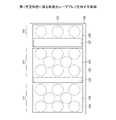
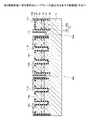
まず、第1実施形態について説明する。第1実施形態は、垂直共振器型面発光レーザ(Vertical Cavity Surface Emitting Laser:VCSEL)アレイに関する。図1は、第1実施形態に係る面発光レーザアレイを示す断面図である。図2は、第1実施形態に係る面発光レーザアレイを示す等価回路図である。図3は、第1実施形態に係る面発光レーザアレイを示す平面図である。(First embodiment)
First, the first embodiment will be described. The first embodiment relates to a vertical cavity surface emitting laser (VCSEL) array. FIG. 1 is a cross-sectional view showing a surface emitting laser array according to the first embodiment. FIG. 2 is an equivalent circuit diagram showing the surface emitting laser array according to the first embodiment. FIG. 3 is a plan view showing the surface emitting laser array according to the first embodiment.
第1実施形態に係るVCSELアレイ100は、図1に示されるように、基板101と、基板101の上の第1サブアレイ121、第2サブアレイ122と、カソードパッド部129とを有する。図2に示されるように、第1サブアレイ121及び第2サブアレイ122は互いに直列に接続されている。第1サブアレイ121及び第2サブアレイ122は、それぞれ、基板101を通して光Lを出射する2個のVCSEL素子124を含む。第1サブアレイ121内で2個のVCSEL素子124は互いに電気的に並列に接続され、第2サブアレイ122内で2個のVCSEL素子124は互いに電気的に並列に接続されている。カソードパッド部129は、疑似VCSEL素子125を含む。図1及び図3に示されるように、第2サブアレイ122は、第1サブアレイ121とカソードパッド部129との間にある。基板101は、例えばノンドープの半絶縁性のGaAs基板である。 The
VCSEL素子124は、第1導電型を有する第1コンタクト層102と、第1導電型を有する第1多層膜反射鏡103と、共振器104と、第2導電型を有する第2多層膜反射鏡106と、第2導電型を有する第2コンタクト層107とを有する。 The
第1コンタクト層102は基板101の上にある。第1コンタクト層102は、例えば高ドープのGaAs層である。第1サブアレイ121に含まれる2個のVCSEL素子124は1個の第1コンタクト層102を共有し、第2サブアレイ122に含まれる2個のVCSEL素子124は1個の第1コンタクト層を共有する。第1コンタクト層102は第1半導体層の一例である。 A
第1多層膜反射鏡103は第1コンタクト層102の上にある。第1多層膜反射鏡103は、屈折率の異なる2種類の層を交互に含む。例えば、一方の層(高屈折率層)はAl0.2Ga0.8As層であり、他方の層(低屈折率層)はAl0.9Ga0.1As層である。図示を省略するが、第1多層膜反射鏡103は、高屈折率層と低屈折率層との間に、組成が連続的に変化する組成傾斜層を含み、組成傾斜層の中心までを含む各層の光学厚さは、レーザの発振波長をλとしてλ/4である。A
共振器104は第1多層膜反射鏡103の上にある。共振器104は、下スペーサ層と、下スペーサ層の上の活性層と、活性層の上の上スペーサ層とを含む。共振器104の光学長はλである。例えば、発振波長λは940nmである。 The
第2多層膜反射鏡106は共振器104の上にある。第2多層膜反射鏡106は、屈折率の異なる2種類の層を交互に含む。例えば、一方の層(高屈折率層)はAl0.2Ga0.8As層であり、他方の層(低屈折率層)はAl0.9Ga0.1As層である。図示を省略するが、第2多層膜反射鏡106は、高屈折率層と低屈折率層との間に、組成が連続的に変化する組成傾斜層を含み、組成傾斜層の中心までを含む各層の光学厚さは、レーザの発振波長をλとしてλ/4である。第2多層膜反射鏡106における高屈折率層及び低屈折率層のペア数は、第1多層膜反射鏡103における高屈折率層及び低屈折率層のペア数よりも多い。これにより、VCSEL素子124は基板101を通して光Lを出射することができる。A
第2多層膜反射鏡106は選択酸化層105を含む。選択酸化層105は、酸化領域105a及び非酸化領域105bを含む。選択酸化層105のAl組成は周辺の層と比べて高く、例えば、選択酸化層105はAlAs層である。 A
第2コンタクト層107は第2多層膜反射鏡106の上にある。第2コンタクト層107は、例えば高ドープのGaAs層である。第2コンタクト層107は第2半導体層の一例である。 A
疑似VCSEL素子125はVCSEL素子124と同様の積層構造を有する。 Pseudo VCSEL
VCSELアレイ100は、VCSEL素子124及び疑似VCSEL素子125を覆う絶縁層108を有する。絶縁層108は、例えば、SiN層又はSiO2層等である。絶縁層108は、第1サブアレイ121に含まれる2個のVCSEL素子124の第2コンタクト層107を露出する開口108aと、第2サブアレイ122に含まれる2個のVCSEL素子124の第2コンタクト層107を露出する開口108bとを有する。絶縁層108は、疑似VCSEL素子125の第2コンタクト層107を露出する開口を有しない。絶縁層108は、第1サブアレイ121に含まれる第1コンタクト層102を露出する開口108sと、第2サブアレイ122に含まれる第1コンタクト層102を露出する開口108tとを有する。The VCSEL
VCSELアレイ100は、絶縁層108の上の電極109aと、電極109bと、電極109xとを有する。電極109aは、開口108aを通じて、第1サブアレイ121に含まれる2個のVCSEL素子124の第2コンタクト層107に接触する。電極109bは、開口108bを通じて、第2サブアレイ122に含まれる2個のVCSEL素子124の第2コンタクト層107に接触する。電極109bは、コンタクト領域126(図3参照)において、第1サブアレイ121に含まれる第1コンタクト層102にも接触する。電極109xは、カソードパッド部129において絶縁層108の上にあるが、疑似VCSEL素子125の第2コンタクト層107に接触しない。電極109xは、コンタクト領域127(図3参照)において、第2サブアレイ122に含まれる第1コンタクト層102に接触する。コンタクト領域126は開口108sに相当し、コンタクト領域127は開口108tに相当する。電極109a、109b及び109xは、例えばTi膜と、Ti膜の上のPt膜と、Pt膜の上のAu膜とを備えた積層体等である。なお、第1コンタクト層102とのオーミック接続のための下地層と、第2コンタクト層107とのオーミック接続のための下地層とが相違していてもよい。
VCSELアレイ100は、基板101の出射側の面(裏面)に反射防止膜110を有する。反射防止膜110の光学厚さはλ/4である。 The
第1実施形態に係るVCSELアレイ100では、第1サブアレイ121における第1コンタクト層102と、第2サブアレイ122における第2コンタクト層107とは、基板101を介して導通していない。電極109bが、第1サブアレイ121における第1コンタクト層102と、第2サブアレイ122における第2コンタクト層107とを接続する。従って、第1サブアレイ121と第2サブアレイ122とが直列に接続される。このため、第1実施形態によれば、すべてのVCSEL素子124が並列に接続されている場合と比較して、駆動電流を凡そ半分に低減することができる。 In the
また、電極109aと電極109xとの間に電位差を与えれば、VCSELアレイ100を駆動させることができる。従って、第1サブアレイ121、第2サブアレイ122の各々に実装用のアノードパット及びカソードパッドを設ける必要がない。このため、小型化に好適である。また、VCSEL素子124の間での発光部の間隔を小さくし、発光むらを抑制することができる。 Further, the
次に、VCSELアレイ100を含む光源モジュールについて説明する。図4は、VCSELアレイ100を含む光源モジュールの第1例を示す断面図である。図5は、VCSELアレイ100を含む光源モジュールの第2例を示す断面図である。 Next, a light source module including the
光源モジュールの第1例は、図4に示されるように、VCSELアレイ100が実装されたサブマウント150を有する。サブマウント150は、AlNからなる絶縁性基板151と、絶縁性基板151の上の電極152及び153とを有する。電極152は電極109aに対向し、電極153は電極109xに対向する。光源モジュールは、電極152と電極109aとの間と、電極153と電極109xとの間に接合材154を有する。サブマウント150は実装基板の一例である。 A first example of a light source module has a
光源モジュールの製造の際には、VCSELアレイ100は、位置合わせされた状態でジャンクションダウンされて接合される。接合材154は、例えば導電性ペースト、はんだ材料等を用いて形成される。熱や超音波を用いた金属接合により、接合材を用いずに接合面が形成されてもよい。 During the manufacture of the light source module, the
このような第1例では、VCSELアレイ100の電極109aと電極109xとの間に、電極152及び153から電位差が与えられる。 In such a first example, a potential difference is applied between
光源モジュールの第2例では、図5に示されるように、サブマウント150が、第1例の構成に加えて、電極155を有する。電極155は電極109bに対向する。光源モジュールは、電極155と電極109bとの間にも接合材154を有する。他の構成は第1例と同様である。 In a second example of a light source module, as shown in FIG. 5, a
このような第2例でも、VCSELアレイ100の電極109aと電極109xとの間に、電極152及び153から電位差が与えられる。電極155は電流経路に含まれないが、第2サブアレイ122に含まれるVCSEL素子124内で発生した熱が、電極155と、その上の接合材154とを介して効率的にサブマウント150に放出される。 In such a second example as well, a potential difference is applied from the
第1例、第2例のいずれにおいても、光源モジュールの製造の際には、接合材154の間での短絡を防止することが重要である。本実施形態では、2個のVCSEL素子124に1個の電極109a又は109bが対応するため、接合材154の間隔を比較的大きくすることができ、短絡を防止しやすい。 In both the first example and the second example, it is important to prevent a short circuit between the
(第1実施形態の変形例)
ここで、第1実施形態の変形例について説明する。図6は、第1実施形態に係る面発光レーザアレイの変形例を示す平面図である。(Modified example of the first embodiment)
Here, a modified example of the first embodiment will be described. FIG. 6 is a plan view showing a modification of the surface emitting laser array according to the first embodiment.
この変形例では、コンタクト領域126が、第1サブアレイ121と第2サブアレイ122との間ではなく、第1サブアレイ121と第2サブアレイ122とが並ぶ方向に垂直な方向で第1サブアレイ121の側方にある。従って、第1実施形態と比較して、第1サブアレイ121内のVCSEL素子124と第2サブアレイ122内のVCSEL素子124との間の距離が小さい。このため、VCSELアレイ100内のVCSEL素子124の間隔のばらつきが小さくなり、発光むらをより抑制することができる。また、更なる小チップ化が可能となる。 In this modification, the
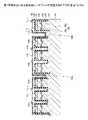
(第2実施形態)
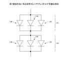
次に、第2実施形態について説明する。第2実施形態は、VCSELアレイに関する。図7は、第2実施形態に係る面発光レーザアレイを示す断面図である。図8は、第2実施形態に係る面発光レーザアレイを示す等価回路図である。(Second embodiment)
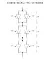
Next, a second embodiment will be described. A second embodiment relates to a VCSEL array. FIG. 7 is a cross-sectional view showing a surface emitting laser array according to the second embodiment. FIG. 8 is an equivalent circuit diagram showing a surface emitting laser array according to the second embodiment.
第2実施形態に係るVCSELアレイ200では、図7に示されるように、第1サブアレイ121及び第2サブアレイ122は、それぞれ、基板101を通して光Lを出射する3個のVCSEL素子124を含む。図8に示されるように、第1サブアレイ121内で3個のVCSEL素子124は互いに電気的に並列に接続され、第2サブアレイ122内で3個のVCSEL素子124は互いに電気的に並列に接続されている。 In the
VCSELアレイ200は、電極109a、109b及び109xを覆う誘電体層111を有する。誘電体層111は、第1サブアレイ121内で電極109aを露出する開口111aと、第2サブアレイ122内で電極109bを露出する開口111bと、カソードパッド部129内で電極109xを露出する開口111xとを有する。開口111aは凡そ第1サブアレイ121内の3個のVCSEL素子124のうち中央に位置するものの上方にある。開口111bは凡そ第2サブアレイ122内の3個のVCSEL素子124のうち中央に位置するものの上方にある。開口111xは疑似VCSEL素子125の上方にある。電極109aの開口111aから露出した部分、電極109bの開口111bから露出した部分及び電極109xの開口111xから露出した部分が実装パッドとして機能する。誘電体層111は、例えば、SiN層又はSiO2層等である。
他の構成は第1実施形態と同様である。 Other configurations are the same as those of the first embodiment.
第2実施形態では、設計者は、実装パッドの位置をVCSEL素子124の発光点から独立して設計することができる。例えば、隣り合う第1サブアレイ121、第2サブアレイ122の間におけるVCSEL素子124の発光点の間隔は、隣り合う実装パッドの間隔よりも小さい。このため、発光むらがより抑制される。 In the second embodiment, the designer can design the mounting pad position independently from the light emitting point of the
次に、VCSELアレイ200を含む光源モジュールについて説明する。図9は、VCSELアレイ200を含む光源モジュールを示す断面図である。 Next, a light source module including the
光源モジュールは、図9に示されるように、VCSELアレイ200が実装されたサブマウント150を有する。サブマウント150は、絶縁性基板151と、絶縁性基板151の上の電極152、153及び155と、誘電体層156とを有する。電極152、153及び155の誘電体層156から露出した部分が第2実装パッドとして機能する。例えば、第1サブアレイ121の実装パッドと電極152の第2実装パッドとは同一の平面形状を有する。例えば、第2サブアレイ122の実装パッドと電極155の第2実装パッドとは同一の平面形状を有する。例えば、カソードパッド部129の実装パッドと電極153の第2実装パッドとは同一の平面形状を有する。接合材154は、例えばSn-Ag-Cu等のはんだである。 The light source module has a
このような光源モジュールでは、VCSELアレイ200とサブマウント150とが接合される接合領域は、誘電体層111及び156に依存し、VCSEL素子124の発光部は接合領域の影響を受けない。上記のように、例えば、隣り合う第1サブアレイ121、第2サブアレイ122の間におけるVCSEL素子124の発光点の間隔は、隣り合う実装パッドの間隔よりも小さい。この場合、接合材154同士の短絡が防止され、かつ発光点の間隔が狭くされ得る。このため、発光むらがより抑制される。また、上記の第2例と同様に、良好な放熱特性が得られる。 In such a light source module, the bonding area where the
一般に、VCSEL素子124はリソグラフィ技術と半導体プロセスによって形成され、接合材154の間隔はVCSEL素子124の間隔よりも大きくなりやすい。本実施形態によれば、実装パッドの間隔に制限されることなくVCSEL素子124の発光部が配置され得る。 In general, the
(第3実施形態)
次に、第3実施形態について説明する。第3実施形態は、VCSELアレイに関する。図10は、第3実施形態に係る面発光レーザアレイを示す断面図である。(Third embodiment)
Next, a third embodiment will be described. A third embodiment relates to a VCSEL array. FIG. 10 is a cross-sectional view showing a surface emitting laser array according to the third embodiment.
第3実施形態に係るVCSELアレイ300は、図10に示されるように、開口111a内、開口111b内及び開口111x内にはんだ膜112を有する。はんだ膜112は、例えば蒸着又はスパッタリング等により成膜される。第3実施形態では、はんだ膜112が実装パッドとして機能する。 The
他の構成は第2実施形態と同様である。 Other configurations are the same as those of the second embodiment.
第3実施形態によっても第2実施形態と同様の効果が得られる。また、サブマウント150への実装が簡易になる。 Effects similar to those of the second embodiment can be obtained by the third embodiment. In addition, mounting on the
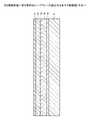
次に、第3実施形態に係るVCSELアレイ300の製造方法について説明する。図11~図18は、第3実施形態に係る面発光レーザアレイの製造方法を示す断面図である。図19~図20は、第3実施形態に係る面発光レーザアレイの製造方法を示す平面図である。図12は、図19中のXII-XII線に沿った断面図に相当し、図14は、図20中のXIV-XIV線に沿った断面図に相当する。 Next, a method for manufacturing the
まず、図11に示されるように、基板101上に、第1コンタクト層102、第1多層膜反射鏡103、共振器104、第2多層膜反射鏡106及び第2コンタクト層107が順次成長される。第1コンタクト層102、第1多層膜反射鏡103、共振器104、第2多層膜反射鏡106及び第2コンタクト層107の半導体積層構造体は、例えば、有機金属気相成長(Metal Organic Chemical Vapor Deposition:MOCVD)法又は分子線エピタキシャル成長(Molecular Beam Epitaxy:MBE)法による結晶成長によって作製される。ここでは、MOCVD法を用いた例が示される。一例として、III族の原料に、トリメチルアルミニウム(TMA)、トリメチルガリウム(TMG)、トリメチルインジウム(TMI)等が用いられ、V族の原料に、アルシン(AsH3)、フォスフィン(PH3)が用いられる。一例として、p型ドーパントの原料には四臭化炭素(CBr4)が用いられ、n型ドーパントの原料にはモノシラン(SiH4)が用いられる。First, as shown in FIG. 11, on a
基板101としては、例えば、半絶縁性GaAs基板が用いられる。 As the
第1コンタクト層102は、例えば厚さが3μmのn型GaAs層である。第1コンタクト層102のオーバーエッチを防止するために、第1コンタクト層102と第1多層膜反射鏡103との間にAlGaInP層又はGaInP層等のエッチストップ層が形成されてもよい。 The
第1多層膜反射鏡103は24.5ペアの高屈折率層及び低屈折率層を含む。例えば、高屈折率層はn型のAl0.2Ga0.8As層であり、低屈折率層はn型のAl0.9Ga0.1As層である。高屈折率層と低屈折率層との間には、電気抵抗を低減するため、厚さが20nmの組成傾斜層が形成される。高屈折率層及び低屈折率層の光学厚さは、発振波長をλとしたとき、隣接する組成傾斜層の1/2を含んでλ/4である。光学厚さがλ/4のとき、その層の実際の厚さDは、D=λ/4n(但し、nはその層の媒質の屈折率)である。The
共振器104は、下スペーサ層と、下スペーサ層の上の活性層と、活性層の上の上スペーサ層とを含む。共振器104の光学長はλである。例えば、発振波長λは940nmである。下スペーサ層及び上スペーサ層は、例えばAl0.4Ga0.6As層である。活性層は3重量子井戸構造からなる。各量子井戸層はInGaAs層であり、各障壁層はAl0.1GaAs層である。活性層は、共振器104の中央に形成される。例えば、発振波長λは940nmである。
第2多層膜反射鏡106は38ペアの高屈折率層及び低屈折率層を含む。例えば、高屈折率層はp型のAl0.2Ga0.8As層であり、低屈折率層はp型のAl0.9Ga0.1As層である。高屈折率層と低屈折率層との間には、電気抵抗を低減するため、厚さが20nmの組成傾斜層が形成される。高屈折率層及び低屈折率層の光学厚さは、発振波長をλとしたとき、隣接する組成傾斜層の1/2を含んでλ/4である。The
第2多層膜反射鏡106は、例えばp-AlAsからなる選択酸化層105(図示せず)を含む。選択酸化層105の位置は、第2多層膜反射鏡106と共振器104との界面から光学的距離がλ/4の位置である。選択酸化層105が上下に組成傾斜層又は中間層等を含んでもよい。 The
第2コンタクト層107は、例えばp型GaAs層である。 The
半導体積層構造体の形成後、写真製版技術を用いて、例えば一辺の長さが30μmの正方形のレジストパターンと、80μm×200μmの長方形のレジストパターンが、第2コンタクト層107の上に形成される。正方形のレジストパターンはVCSEL素子124の形成予定領域に形成され、長方形のレジストパターンは疑似VCSEL素子125の形成予定領域に形成される。次に、これらレジストパターンをマスクとし、Cl2ガスを用いた電子サイクロトロン(Electron Cyclotron Resonance:ECR)エッチング法により、図12及び図19に示されるように、第1コンタクト層102が底面として露出するように半導体積層構造体がエッチングされる。この結果、メサ構造体が形成される。メサ構造体は、少なくとも選択酸化層105(図示せず)が露出するように形成される。エッチング後、レジストパターンが除去される。After forming the semiconductor laminated structure, a square resist pattern with a side length of 30 μm and a rectangular resist pattern of 80 μm×200 μm, for example, are formed on the
次に、メサ構造体が形成された半導体積層構造体を酸化対象物として、水蒸気中で熱処理(酸化処理)が行われる。この結果、メサ構造体の外周部から選択酸化層105中のAlが選択的に酸化される。そして、図13に示すように、メサ構造体の中央部に、Alの酸化領域101aによって囲まれた酸化されていない非酸化領域105bが残留する。これにより、発光部の駆動電流の経路をメサ構造体の中央部だけに制限する、酸化狭窄構造体が形成される。非酸化領域105bが電流通過領域(電流注入領域)である。このようにして、例えば一片の長さが10μmの正方形状の電流通過領域が形成される。 Next, a heat treatment (oxidation treatment) is performed in steam using the semiconductor laminated structure having the mesa structure formed thereon as an object to be oxidized. As a result, Al in the
次に、写真製版技術を用いてレジストパターンが第1コンタクト層102及び第2コンタクト層107の上に形成される。レジストパターンは、第1サブアレイ121の形成予定領域と第2サブアレイ122の形成予定領域との間と、第2サブアレイ122の形成予定領域とカソードパッド部129の形成予定領域との間とに開口を有する。開口の幅は、例えば20μmである。次に、これらレジストパターンをマスクとし、Cl2ガスを用いたECRエッチング法により、図14及び図20に示されるように、基板101が底面として露出するように第1コンタクト層102がエッチングされる。この結果、第1コンタクト層102に幅が20μmの溝が形成される。溝により、第1サブアレイ121内の第1コンタクト層102と、第2サブアレイ122内の第1コンタクト層102と、カソードパッド部129内の第1コンタクト層102とが電気的に絶縁される。溝は、溶剤を用いたウェットエッチング法により形成されてもよい。Next, a resist pattern is formed on the
次に、図15に示されるように、例えばプラズマ化学気相成長(Chemical Vapor Deposition:CVD)法を用いて、メサ構造体を覆う光学的に透明な絶縁層108が形成される。絶縁層108は、例えばSiN層である。次に、写真製版技術を用い、BHF(バッファードフッ酸)等を用いたエッチングによって絶縁層108に、開口108a及び108bと、開口108s及び108tとが形成される。 Next, as shown in FIG. 15, an optically transparent insulating
次に、写真製版技術によるレジストパターンの形成、金属膜の形成及びリフトオフが行われ、図16に示されるように、電極109a、109b及び109xが形成される。金属膜は、例えばTi膜と、Ti膜の上のPt膜と、Pt膜の上のAu膜とを備えた積層体等である。第1コンタクト層102とのオーミック接続のための下地層と、第2コンタクト層107とのオーミック接続のための下地層とが相違していてもよい。この場合、蒸着及びリフトオフが2回又は3回に分けて行われてもよい。 Next, formation of a resist pattern, formation of a metal film and lift-off are performed by photomechanical technology to form
次に、図17に示されるように、例えばプラズマCVD法を用いて、電極109a、109b及び109xを覆う光学的に透明な誘電体層111が形成される。誘電体層111は、例えばSiN層である。次に、写真製版技術を用い、BHF(バッファードフッ酸)等を用いたエッチングによって誘電体層111に、開口111a、111b及び111xが形成される。 Next, as shown in FIG. 17, an optically transparent
次に、図18に示されるように、次に、はんだ膜112が形成される。はんだ膜112の形成では、まず、シード層(図示せず)がスパッタリング法等により形成される。シード層は、例えば、Ti膜と、Ti膜の上のCu膜とを含む。次に、シード層の上に、写真製版技術を用いてレジストパターンが形成される。レジストパターンはサブマウント150との実装に用いる実装領域のみを開口する。隣り合う開口の間の距離は、例えば200μmである。この距離は、隣り合う実装パッドの間での短絡が生じないよう、その後の実装工程を考慮して設定されることが望ましい。次に、電解めっき法により開口内に選択的にはんだ膜112が形成される。はんだ膜112の材料は、例えばSnAg、SnAgCu、SuAu等である。シード層とはんだ膜112との間にNi層又はCr層等の密着層が形成されてもよい。はんだ膜112の形成後、レジストパターンが除去され、全面の逆スパッタリング等によるエッチバックが行われ、露出したシード層が除去される。 Next, as shown in FIG. 18, a
次に、基板101の出射側の面(裏面)が化学機械的研磨(Chemical Mechanical Polishing:CMP)法等により鏡面化される。次に、基板101の出射側の面に反射防止膜110が形成される。反射防止膜110は、例えばプラズマCVD法により形成される。反射防止膜110は、例えば光学厚さがλ/4のSiN膜である。 Next, the exit side surface (rear surface) of the
このようにして、第3実施形態に係るVCSELアレイ300が製造される。 Thus, the
(第4実施形態)
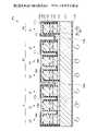
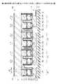
次に、第4実施形態について説明する。第4実施形態は、VCSELアレイに関する。図21は、第4実施形態に係る面発光レーザアレイを示す断面図である。図22は、第4実施形態に係る面発光レーザアレイを示す等価回路図である。(Fourth embodiment)
Next, a fourth embodiment will be described. A fourth embodiment relates to a VCSEL array. FIG. 21 is a cross-sectional view showing a surface emitting laser array according to the fourth embodiment. FIG. 22 is an equivalent circuit diagram showing a surface emitting laser array according to the fourth embodiment.
第4実施形態に係るVCSELアレイ400は、図21に示されるように、基板101と、基板101の上の第1サブアレイ121、第2サブアレイ122と、第3サブアレイ123と、カソードパッド部129とを有する。図22に示されるように、第1サブアレイ121、第2サブアレイ122及び第3サブアレイ123は互いに直列に接続されている。第1サブアレイ121、第2サブアレイ122及び第3サブアレイ123は、それぞれ、基板101を通して光Lを出射する2個のVCSEL素子124を含む。第1サブアレイ121内で2個のVCSEL素子124は互いに電気的に並列に接続され、第2サブアレイ122内で2個のVCSEL素子124は互いに電気的に並列に接続され、第3サブアレイ123内で2個のVCSEL素子124は互いに電気的に並列に接続されている。図21に示されるように、第3サブアレイ123は、第2サブアレイ122とカソードパッド部129との間にある。 A
絶縁層108は、開口108a及び108bに加えて、第3サブアレイ123に含まれる2個のVCSEL素子124の第2コンタクト層107を露出する開口108cを有する。絶縁層108は、開口108s及び108tに加えて、第3サブアレイ123に含まれる第1コンタクト層102を露出する開口108uを有する。 The insulating
VCSELアレイ100は、電極109a、109b及び109xに加えて、絶縁層108の上の電極109cを有する。電極109cは、開口108cを通じて、第3サブアレイ123に含まれる2個のVCSEL素子124の第2コンタクト層107に接触する。
誘電体層111は、開口111a及び111xを有するが、開口111bを有しない。従って、誘電体層111は、電極109b及び109cの全体を覆う。VCSELアレイ400は、開口111a内及び開口111x内にはんだ膜112を有する。VCSELアレイ400は、更に、第2サブアレイ122及び第3サブアレイ123にわたって広がるはんだ膜112cを有する。はんだ膜112cは、第2サブアレイ122と第3サブアレイ123との間の誘電体層111の隙間の内側に入り込んでもよい。第4実施形態では、はんだ膜112及び112cが実装パッドとして機能する。
他の構成は第3実施形態と同様である。 Other configurations are the same as those of the third embodiment.
次に、VCSELアレイ400を含む光源モジュールについて説明する。図23は、VCSELアレイ400を含む光源モジュールを示す断面図である。 Next, a light source module including the
光源モジュールは、図23に示されるように、VCSELアレイ400が実装されたサブマウント150を有する。サブマウント150は、絶縁性基板151と、絶縁性基板151の上の電極152、153及び155と、誘電体層156とを有する。電極152、153及び155の誘電体層156から露出した部分が第2実装パッドとして機能する。例えば、第1サブアレイ121の実装パッドと電極152の第2実装パッドとは同一の平面形状を有する。例えば、第2サブアレイ122及び第3サブアレイ123の実装パッド(はんだ膜112c)と電極155の第2実装パッドとは同一の平面形状を有する。例えば、カソードパッド部129の実装パッドと電極153の第2実装パッドとは同一の平面形状を有する。 The light source module has a
第4実施形態によっても第3実施形態と同様の効果が得られる。また、第2サブアレイ122と第3サブアレイ123とを電気的に短絡させることなく、実装パッドが1つに纏められる。従って、サブアレイの数と実装パッドの数とが等しい。電極155は電流経路に含まれないが、第2サブアレイ122に含まれるVCSEL素子124内で発生した熱及び第3サブアレイ123に含まれるVCSEL素子124内で発生した熱が、電極155と、その上の接合材154とを介して効率的にサブマウント150に放出される。第4実施形態では、第2サブアレイ122と第3サブアレイ123との間に実装パッドの隙間が必要とされず、大きな面積の接合領域が得られ、より優れた放熱特性が得られる。 Effects similar to those of the third embodiment can also be obtained by the fourth embodiment. In addition, the mounting pads of the
なお、第4実施形態に係るVCSELアレイ400は、3個のサブアレイを有するが、サブアレイの数が4個以上であっても、実装パッドの数を3個とすることができる。例えば、サブアレイの数が4個又は5個であっても、VCSELアレイが、第1サブアレイ121の実装パッドと、カソードパッド部129の実装パッドと、電流経路に含まれない放熱用の実装パッドとを有してもよい。このような場合、実装パッドの数はサブアレイの数よりも少ない。また、例えば、サブアレイの数が5個である場合に、電流経路に含まれず、電気的に接続されない実装パッドが2つの領域に分割され、実装パッドの数が4個になっていてもよい。 Although the
なお、隣り合う第1コンタクト層102の間の絶縁分離が、エッチングによる溝の形成に代えて、水素等のイオン注入により行われてもよい。 Note that the insulating separation between adjacent first contact layers 102 may be performed by ion implantation of hydrogen or the like instead of forming grooves by etching.
また、上記の実施形態では、半導体積層構造体と基板101とを電気的に絶縁するために、基板101が半絶縁性GaAs基板であるが、基板101は半絶縁性GaAs基板に限定されない。例えば、基板101と第1コンタクト層102との間にノンドープのGaAs層があれば、基板101がn型GaAs基板であってもよい。 In the above embodiment, the
(第5実施形態)
次に、第5実施形態について説明する。第5実施形態は測距装置に関する。測距装置は光学装置の一例である。図24は、第5実施形態に係る測距装置を示す図である。(Fifth embodiment)
Next, a fifth embodiment will be described. The fifth embodiment relates to a distance measuring device. A rangefinder is an example of an optical device. FIG. 24 is a diagram showing a distance measuring device according to the fifth embodiment.
第5実施形態に係る測距装置500は、投光部510、受光部520、時間計測回路530及び制御回路540を有する。 A
投光部510は、例えば、光源511と、光源駆動回路512と、光スキャナ513と、光スキャナ駆動回路514と、走査角モニタ515と、投射レンズ516とを有する。光源511は、第1~第4実施形態に係るVCSELアレイを有する光源モジュールを含む。光源駆動回路512は制御回路540から出力された駆動信号に基づいて光源511を駆動する。光スキャナ513はMEMS(Micro Electro Mechanical System)ミラー又はポリゴンミラー等を含む。光スキャナ駆動回路514は制御回路540から出力された駆動信号に基づいて光スキャナ513を駆動する。光源511の光源モジュールは複数のサブアレイを有する。各サブアレイは、それぞれが1個以上のVCSEL素子を含み、各サブアレイ内のVCSEL素子は電気的に並列に接続されている。また、各サブアレイは、光スキャナ513の走査方向(副走査方向に)1次元的に配置されている。光源511の光源モジュールは光源駆動回路512によって、例えばナノ秒オーダーのパルス電流で駆動される。そして、VCSEL素子が出射したレーザ光は必要に応じて投射レンズ516等によって所望のビームプロファイルに変換され、その後、光スキャナ513によって照射方向が決められ、測距装置500の外部へ照射される。光スキャナ513の走査角が走査角モニタ515により測定され、この結果が制御回路540に出力される。光スキャナ513及び投射レンズ516は光学素子の一例である。 The
測距装置500の外部へと照射されたレーザ光は、対称物によって反射されて測距装置500に戻り、受光部520に到達する。 The laser beam irradiated to the outside of the
受光部520は、例えば、受光素子521と、受光レンズ522と、バンドパスフィルタ523とを有する。受光素子521はシリコンのAPD(Avalanche Photo Diode)素子を含む。受光レンズ522は受光部520に到達した光を受光素子521に収束させる。バンドパスフィルタ523は誘電体多層膜を含み、光源511の発振波長の領域の光のみを透過するように設計されている。バンドパスフィルタ523により、信号のS/N比を向上させることができる。 The
受光素子521に到達した光は、受光素子521により電気信号に変換され、必要に応じて増幅器531やコンパレータ532を通して時間計測回路530に入力される。 The light that reaches the light receiving element 521 is converted into an electric signal by the light receiving element 521 and input to the
時間計測回路530には、制御回路540が出力した光源511の駆動信号と、受光素子521からの信号が入力される。時間計測回路530は、これら2信号の間の遅延時間を計測し、この結果を制御回路540に出力する。 The drive signal for the
制御回路540は、時間計測回路530からの遅延時間を光波長へと変換する。
このような測距装置500によれば、対象物までの距離を計測し、光源モジュールのサブ発光領域及び光スキャナ513によって分解された空間領域に対して、順次レーザ光を照射することで、2次元的な距離情報を得ることができる。この測距装置500は、例えばLiDAR(Light Detection and Ranging)に用いることができる。 According to such a
本開示の光源モジュールは、測距装置の光源の他にも、固体レーザの励起光源に用いることもできる。また、面発光レーザモジュールを、蛍光体等の、面発光レーザモジュールからの出射光の波長変換を行う光学素子と組み合わせてプロジェクタ等の光源装置として利用することもできる。面発光レーザモジュールを、レンズ、ミラー、回折格子等の、面発光レーザモジュールからの出射光を発散又は収束させる光学素子と組み合わせてセンシング用の光源装置として利用することもできる。 The light source module of the present disclosure can also be used as an excitation light source for solid-state lasers in addition to the light source for rangefinders. Further, the surface emitting laser module can be used as a light source device such as a projector by combining it with an optical element such as a phosphor that converts the wavelength of light emitted from the surface emitting laser module. The surface emitting laser module can also be used as a light source device for sensing in combination with an optical element such as a lens, mirror, or diffraction grating that diverges or converges the emitted light from the surface emitting laser module.
以上、好ましい実施の形態等について詳説したが、上述した実施の形態等に制限されることはなく、特許請求の範囲に記載された範囲を逸脱することなく、上述した実施の形態等に種々の変形及び置換を加えることができる。 Although the preferred embodiments and the like have been described in detail above, the present invention is not limited to the above-described embodiments and the like, and various modifications can be made to the above-described embodiments and the like without departing from the scope of the claims. Modifications and substitutions can be made.
100、200、300、400、 面発光レーザアレイ(VCSELアレイ)
101 基板
102、107 コンタクト層
103、106 多層膜反射鏡
104 共振器
105 選択酸化層
109a、109b、109c、109x 電極
121、122、123 サブアレイ
124 VCSEL素子
125 疑似VCSEL素子
129 カソードパッド部
150 サブマウント
500 測距装置100, 200, 300, 400, surface emitting laser array (VCSEL array)
101
Claims (9)
Translated fromJapanese前記基板上に設けられ、前記基板を通して光を出射し、互いに電気的に並列に接続された複数の面発光レーザ素子を含む複数のサブアレイと、
を有し、
前記面発光レーザ素子は、それぞれ、
第1導電型の第1半導体層と、
第2導電型の第2半導体層と、
前記第1半導体層と前記第2半導体層との間に設けられた共振器と、
を有し、
隣り合う前記サブアレイは、一方の前記サブアレイに含まれる複数の前記面発光レーザ素子内の前記第1半導体層と、他方の前記サブアレイに含まれる複数の前記面発光レーザ素子内の前記第2半導体層とを共通に接続する電極を有しており、
前記複数のサブアレイが電気的に直列に接続されることを特徴とする面発光レーザアレイ。a substrate;
a plurality of sub-arrays provided on the substrate, emitting light through the substrate, and including a plurality of surface-emitting laser elements electrically connected in parallel;
has
Each of the surface emitting laser elements is
a first semiconductor layer of a first conductivity type;
a second semiconductor layer of a second conductivity type;
a resonator provided between the first semiconductor layer and the second semiconductor layer;
has
In the adjacent subarrays, the first semiconductor layers in the plurality of surface emitting laser elements included in one of the subarrays and the second semiconductor layers in the plurality of surface emitting laser elements included in the other subarray. has an electrode that commonly connects the
A surface emitting laser array, wherein the plurality of subarrays are electrically connected in series.
隣り合う前記サブアレイの間における前記面発光レーザ素子の発光点の間隔は、隣り合う前記実装パッドの間隔よりも小さいことを特徴とする請求項1に記載の面発光レーザアレイ。one or more of the plurality of sub-arrays are provided with mounting pads to be mounted on a mounting substrate;
2. The surface emitting laser array according to claim 1, wherein the distance between the light emitting points of said surface emitting laser elements between said adjacent sub-arrays is smaller than the distance between said adjacent mounting pads.
前記電極に接続された導通パッドと、
前記電極から絶縁された非導通パッドと、
を有することを特徴とする請求項2乃至4のいずれか1項に記載の面発光レーザアレイ。The mounting pad is
a conductive pad connected to the electrode;
a non-conducting pad insulated from the electrode;
5. The surface emitting laser array according to any one of claims 2 to 4, characterized by having:
前記面発光レーザアレイが実装された実装基板と、
を有することを特徴とする光源モジュール。a surface emitting laser array according to any one of claims 1 to 6;
a mounting substrate on which the surface emitting laser array is mounted;
A light source module comprising:
前記面発光レーザアレイに設けられた実装パッドに接続され、当該実装パッドと同一の平面形状の第2実装パッドを有することを特徴とする請求項7に記載の光源モジュール。The mounting board is
8. The light source module according to claim 7, further comprising a second mounting pad connected to the mounting pad provided on the surface emitting laser array and having the same planar shape as the mounting pad.
前記光源モジュールから出射された光が入射される光学素子と、
を有することを特徴とする測距装置。A light source module according to claim 7 or 8;
an optical element into which light emitted from the light source module is incident;
A rangefinder, characterized by comprising:
Priority Applications (8)
| Application Number | Priority Date | Filing Date | Title |
|---|---|---|---|
| JP2021040536AJP7683252B2 (en) | 2021-03-12 | 2021-03-12 | Surface emitting laser array, light source module and distance measuring device |
| KR1020237030251AKR20230138529A (en) | 2021-03-12 | 2022-02-08 | Surface-emitting laser array, light source module, and distance measuring device |
| US18/277,387US20240128725A1 (en) | 2021-03-12 | 2022-02-08 | Surface-emitting laser array, light source module, and distance-measuring apparatus |
| CN202280019589.2ACN117063358A (en) | 2021-03-12 | 2022-02-08 | Surface-emitting laser array, light source module, and distance measuring device |
| EP22705144.8AEP4305716A1 (en) | 2021-03-12 | 2022-02-08 | Surface-emitting laser array, light source module, and distance-measuring apparatus |
| PCT/IB2022/051096WO2022189869A1 (en) | 2021-03-12 | 2022-02-08 | Surface-emitting laser array, light source module, and distance-measuring apparatus |
| CA3210713ACA3210713A1 (en) | 2021-03-12 | 2022-02-08 | Surface-emitting laser array, light source module, and distance-measuring apparatus |
| TW111105089ATWI885240B (en) | 2021-03-12 | 2022-02-11 | Surface-emitting laser array, light source module, and distance-measuring apparatus |
Applications Claiming Priority (1)
| Application Number | Priority Date | Filing Date | Title |
|---|---|---|---|
| JP2021040536AJP7683252B2 (en) | 2021-03-12 | 2021-03-12 | Surface emitting laser array, light source module and distance measuring device |
Publications (2)
| Publication Number | Publication Date |
|---|---|
| JP2022139943Atrue JP2022139943A (en) | 2022-09-26 |
| JP7683252B2 JP7683252B2 (en) | 2025-05-27 |
Family
ID=80787109
Family Applications (1)
| Application Number | Title | Priority Date | Filing Date |
|---|---|---|---|
| JP2021040536AActiveJP7683252B2 (en) | 2021-03-12 | 2021-03-12 | Surface emitting laser array, light source module and distance measuring device |
Country Status (8)
| Country | Link |
|---|---|
| US (1) | US20240128725A1 (en) |
| EP (1) | EP4305716A1 (en) |
| JP (1) | JP7683252B2 (en) |
| KR (1) | KR20230138529A (en) |
| CN (1) | CN117063358A (en) |
| CA (1) | CA3210713A1 (en) |
| TW (1) | TWI885240B (en) |
| WO (1) | WO2022189869A1 (en) |
Cited By (1)
| Publication number | Priority date | Publication date | Assignee | Title |
|---|---|---|---|---|
| WO2024241740A1 (en)* | 2023-05-19 | 2024-11-28 | ソニーセミコンダクタソリューションズ株式会社 | Surface light-emitting element and light source device |
Families Citing this family (3)
| Publication number | Priority date | Publication date | Assignee | Title |
|---|---|---|---|---|
| US20230130341A1 (en)* | 2020-04-02 | 2023-04-27 | Shenzhen Raysees Ai Technology Co. Ltd. | Bottom-emitting multijunction vcsel array |
| CN117013369A (en)* | 2023-09-28 | 2023-11-07 | 深圳市柠檬光子科技有限公司 | Laser chip, manufacturing method thereof and laser device |
| DE102023133376A1 (en)* | 2023-11-29 | 2025-06-05 | Trumpf Photonic Components Gmbh | Laser array with light emission through the substrate and method for producing the laser array |
Citations (7)
| Publication number | Priority date | Publication date | Assignee | Title |
|---|---|---|---|---|
| US20130163626A1 (en)* | 2011-12-24 | 2013-06-27 | Princeton Optronics | Optical Illuminator |
| JP2014093463A (en)* | 2012-11-06 | 2014-05-19 | Fuji Xerox Co Ltd | Surface emitting semiconductor laser array device, light source and light source module |
| JP2014150225A (en)* | 2013-02-04 | 2014-08-21 | Fuji Xerox Co Ltd | Semiconductor light-emitting element |
| JP2015510279A (en)* | 2012-03-14 | 2015-04-02 | コーニンクレッカ フィリップス エヌ ヴェ | VCSEL module and manufacturing method thereof |
| JP2016018943A (en)* | 2014-07-10 | 2016-02-01 | 株式会社リコー | Surface-emitting laser array and laser device |
| JP2020529128A (en)* | 2017-07-25 | 2020-10-01 | トリルミナ コーポレーション | Single chip series connection VCSEL array |
| US20200313401A1 (en)* | 2019-04-01 | 2020-10-01 | Lumentum Operations Llc | Electrically isolating vertical-emitting devices |
Family Cites Families (5)
| Publication number | Priority date | Publication date | Assignee | Title |
|---|---|---|---|---|
| US11482835B2 (en)* | 2017-07-25 | 2022-10-25 | Lumentum Operations Llc | VCSEL device with multiple stacked active regions |
| KR101981756B1 (en) | 2017-09-27 | 2019-05-27 | 주식회사 휴비스 | Composite Melting-yarn having excellent tactility and dyeing property, And Method preparing same |
| JP7247615B2 (en) | 2019-01-31 | 2023-03-29 | 株式会社リコー | Surface emitting laser module, optical device and surface emitting laser substrate |
| KR20200123710A (en) | 2019-04-22 | 2020-10-30 | 이성우 | Automatic umbrella |
| JP7404724B2 (en) | 2019-09-10 | 2023-12-26 | 日本製紙株式会社 | Mochi-like food and method for producing mochi-like food |
- 2021
- 2021-03-12JPJP2021040536Apatent/JP7683252B2/enactiveActive
- 2022
- 2022-02-08USUS18/277,387patent/US20240128725A1/enactivePending
- 2022-02-08KRKR1020237030251Apatent/KR20230138529A/enactivePending
- 2022-02-08WOPCT/IB2022/051096patent/WO2022189869A1/ennot_activeCeased
- 2022-02-08EPEP22705144.8Apatent/EP4305716A1/enactivePending
- 2022-02-08CACA3210713Apatent/CA3210713A1/enactivePending
- 2022-02-08CNCN202280019589.2Apatent/CN117063358A/enactivePending
- 2022-02-11TWTW111105089Apatent/TWI885240B/enactive
Patent Citations (7)
| Publication number | Priority date | Publication date | Assignee | Title |
|---|---|---|---|---|
| US20130163626A1 (en)* | 2011-12-24 | 2013-06-27 | Princeton Optronics | Optical Illuminator |
| JP2015510279A (en)* | 2012-03-14 | 2015-04-02 | コーニンクレッカ フィリップス エヌ ヴェ | VCSEL module and manufacturing method thereof |
| JP2014093463A (en)* | 2012-11-06 | 2014-05-19 | Fuji Xerox Co Ltd | Surface emitting semiconductor laser array device, light source and light source module |
| JP2014150225A (en)* | 2013-02-04 | 2014-08-21 | Fuji Xerox Co Ltd | Semiconductor light-emitting element |
| JP2016018943A (en)* | 2014-07-10 | 2016-02-01 | 株式会社リコー | Surface-emitting laser array and laser device |
| JP2020529128A (en)* | 2017-07-25 | 2020-10-01 | トリルミナ コーポレーション | Single chip series connection VCSEL array |
| US20200313401A1 (en)* | 2019-04-01 | 2020-10-01 | Lumentum Operations Llc | Electrically isolating vertical-emitting devices |
Cited By (1)
| Publication number | Priority date | Publication date | Assignee | Title |
|---|---|---|---|---|
| WO2024241740A1 (en)* | 2023-05-19 | 2024-11-28 | ソニーセミコンダクタソリューションズ株式会社 | Surface light-emitting element and light source device |
Also Published As
| Publication number | Publication date |
|---|---|
| CA3210713A1 (en) | 2022-09-15 |
| CN117063358A (en) | 2023-11-14 |
| TW202236765A (en) | 2022-09-16 |
| TWI885240B (en) | 2025-06-01 |
| EP4305716A1 (en) | 2024-01-17 |
| US20240128725A1 (en) | 2024-04-18 |
| KR20230138529A (en) | 2023-10-05 |
| JP7683252B2 (en) | 2025-05-27 |
| WO2022189869A1 (en) | 2022-09-15 |
Similar Documents
| Publication | Publication Date | Title |
|---|---|---|
| JP7683252B2 (en) | Surface emitting laser array, light source module and distance measuring device | |
| US9252562B2 (en) | Surface emitting semiconductor laser, surface emitting semiconductor laser array, surface emitting semiconductor laser device, optical transmission device, information processing apparatus, and method of producing surface emitting semiconductor laser | |
| JP7480873B2 (en) | Surface emitting laser module, optical device and distance measuring device | |
| JP4656183B2 (en) | Semiconductor light emitting device | |
| US8175128B2 (en) | Semiconductor laser element and semiconductor laser device | |
| JP7200721B2 (en) | Surface emitting laser module, light source device, detection device | |
| US12068577B2 (en) | Surface emitting laser, surface emitting laser device, light source device, and detection apparatus | |
| US20230006421A1 (en) | Vertical cavity surface emitting laser element, vertical cavity surface emitting laser element array, vertical cavity surface emitting laser module, and method of producing vertical cavity surface emitting laser element | |
| JP7434849B2 (en) | Surface emitting laser, surface emitting laser device, light source device and detection device | |
| JP2022500880A (en) | Phase-coupled laser devices and methods for manufacturing phase-coupled laser devices. | |
| JP4650631B2 (en) | Semiconductor light emitting device | |
| US11901701B2 (en) | Surface emitting laser element, surface emitting laser, surface emitting laser device, light source device, and detection apparatus | |
| JP7351132B2 (en) | Surface emitting laser, surface emitting laser device, light source device and detection device | |
| JP4977992B2 (en) | Semiconductor light emitting device and manufacturing method thereof | |
| JP2006190762A (en) | Semiconductor laser | |
| JP7556888B2 (en) | Light emitting device and method for manufacturing the same | |
| US7643531B2 (en) | Optical semiconductor element including photodetecting element with comb-tooth structure | |
| WO2024262206A1 (en) | Light emitting device and method for manufacturing same | |
| CN119866427A (en) | VCSEL element, sensor device, electronic device and user interface |
Legal Events
| Date | Code | Title | Description |
|---|---|---|---|
| A621 | Written request for application examination | Free format text:JAPANESE INTERMEDIATE CODE: A621 Effective date:20240119 | |
| A977 | Report on retrieval | Free format text:JAPANESE INTERMEDIATE CODE: A971007 Effective date:20240828 | |
| A131 | Notification of reasons for refusal | Free format text:JAPANESE INTERMEDIATE CODE: A131 Effective date:20241001 | |
| A521 | Request for written amendment filed | Free format text:JAPANESE INTERMEDIATE CODE: A523 Effective date:20241202 | |
| A131 | Notification of reasons for refusal | Free format text:JAPANESE INTERMEDIATE CODE: A131 Effective date:20250128 | |
| A521 | Request for written amendment filed | Free format text:JAPANESE INTERMEDIATE CODE: A523 Effective date:20250328 | |
| TRDD | Decision of grant or rejection written | ||
| A01 | Written decision to grant a patent or to grant a registration (utility model) | Free format text:JAPANESE INTERMEDIATE CODE: A01 Effective date:20250415 | |
| A61 | First payment of annual fees (during grant procedure) | Free format text:JAPANESE INTERMEDIATE CODE: A61 Effective date:20250428 | |
| R150 | Certificate of patent or registration of utility model | Ref document number:7683252 Country of ref document:JP Free format text:JAPANESE INTERMEDIATE CODE: R150 |