JP2022132369A - Solid state imaging device - Google Patents
Solid state imaging deviceDownload PDFInfo
- Publication number
- JP2022132369A JP2022132369AJP2022110874AJP2022110874AJP2022132369AJP 2022132369 AJP2022132369 AJP 2022132369AJP 2022110874 AJP2022110874 AJP 2022110874AJP 2022110874 AJP2022110874 AJP 2022110874AJP 2022132369 AJP2022132369 AJP 2022132369A
- Authority
- JP
- Japan
- Prior art keywords
- imaging device
- state imaging
- solid
- substrate
- seal
- Prior art date
- Legal status (The legal status is an assumption and is not a legal conclusion. Google has not performed a legal analysis and makes no representation as to the accuracy of the status listed.)
- Pending
Links
Images


Landscapes
- Solid State Image Pick-Up Elements (AREA)
- Internal Circuitry In Semiconductor Integrated Circuit Devices (AREA)
- Transforming Light Signals Into Electric Signals (AREA)
- Semiconductor Integrated Circuits (AREA)
- Metal-Oxide And Bipolar Metal-Oxide Semiconductor Integrated Circuits (AREA)
Abstract
Translated fromJapaneseDescription
Translated fromJapanese本発明は、複数の部材を貼り合わせて構成する固体撮像装置に関する。 The present invention relates to a solid-state imaging device configured by bonding a plurality of members together.
固体撮像装置において、光電変換部と周辺回路部とを別の基板に分けて形成し、それらをマイクロバンプ等で電気的に接続する構成が知られている。 2. Description of the Related Art In a solid-state imaging device, a configuration is known in which a photoelectric conversion section and a peripheral circuit section are separately formed on separate substrates and electrically connected by microbumps or the like.
特許文献1には、光電変換部や信号読み出し用の読み出し回路を設けた画素を含む第1の半導体基板と、画素から読み出された信号を処理するための周辺回路を含む第2の半導体基板とを貼り合わせた裏面照射型の固体撮像装置が記載されている。 Patent Document 1 discloses a first semiconductor substrate including pixels provided with a photoelectric conversion unit and a readout circuit for reading out signals, and a second semiconductor substrate including a peripheral circuit for processing signals read out from the pixels. A back-illuminated solid-state imaging device is described in which .
各種回路を有する半導体基板は、半導体基板の周囲の雰囲気等から侵入する水分やイオンから素子を保護する必要がある。そこで、特許文献1に記載されるような第1の半導体基板と第2の半導体基板を有する固体撮像装置において、周囲の雰囲気等から侵入する水分やイオンからの保護が求められていた。 2. Description of the Related Art A semiconductor substrate having various circuits needs to protect its elements from moisture and ions entering from the atmosphere around the semiconductor substrate. Therefore, in a solid-state imaging device having a first semiconductor substrate and a second semiconductor substrate as described in Patent Document 1, protection from moisture and ions entering from the surrounding atmosphere has been demanded.
そこで本発明においては、耐湿性が改善された固体撮像装置を提供することを目的とする。 SUMMARY OF THE INVENTION Accordingly, it is an object of the present invention to provide a solid-state imaging device with improved moisture resistance.
本発明の固体撮像装置は、各々が光電変換部及び該光電変換部で生じた信号を処理もしくは該信号を読み出すための読み出し回路を有する複数の画素と、前記複数の画素の信号を読み出すための周辺回路とを有し、前記複数の光電変換部は第1部材に配され、少なくとも前記読み出し回路の一部、及び前記周辺回路が第2部材に配されており、前記光電変換部からの信号を前記第2の部材に配された前記読み出し回路が受けるように前記第1部材と前記第2部材とが貼り合わせられて構成された固体撮像装置であって、前記固体撮像装置の外部から前記複数の画素及び前記周辺回路への水分の浸入を抑制するシール部を有し、該シール部は、前記第1部材に配された第1シール部と、前記第2部材に配された第2シール部とを有し、前記第1シール部の一部と前記第2シール部の一部とが接している。 The solid-state imaging device of the present invention comprises a plurality of pixels each having a photoelectric conversion portion and a readout circuit for processing or reading out signals generated by the photoelectric conversion portion; a peripheral circuit, wherein the plurality of photoelectric conversion units are arranged on a first member, at least part of the readout circuit and the peripheral circuit are arranged on a second member, and a signal from the photoelectric conversion unit a solid-state imaging device configured by bonding the first member and the second member so that the readout circuit disposed on the second member receives the A sealing portion for suppressing entry of moisture into the plurality of pixels and the peripheral circuit is provided, and the sealing portion includes a first sealing portion arranged on the first member and a second sealing portion arranged on the second member. A portion of the first seal portion and a portion of the second seal portion are in contact with each other.
本発明によれば、例えば、外部からの水分の浸入が抑制された固体撮像装置が提供可能である。 According to the present invention, for example, it is possible to provide a solid-state imaging device in which intrusion of moisture from the outside is suppressed.
以下、本発明について図面を用いて詳細に説明を行うなお、実施例の説明において、第1基板の一主面及び第2基板の一主面とは光電変換部もしくはトランジスタが配される基板表面である該主面と対向する反対側の面が、第1基板の裏面及び第2基板の裏面であるまた、特に説明上方向は裏面から主面に向かう方向とし、下方向及び深さ方向は基板の主面から裏面に向かう方向とする。 Hereinafter, the present invention will be described in detail with reference to the drawings. is the back surface of the first substrate and the back surface of the second substrate. In particular, the upward direction is the direction from the back surface to the main surface, and the downward and depth directions are It is the direction from the main surface of the substrate to the back surface.
また本発明においては外部からの水分の侵入を抑制するシール部としてシールリングを例にとり説明するが水分などの侵入を抑制する機能を有していればリング形状に限られるものではない。 Further, in the present invention, a seal ring is used as an example of a seal portion that suppresses the intrusion of moisture from the outside, but the seal portion is not limited to a ring shape as long as it has a function of suppressing the intrusion of moisture or the like.
(実施例1)
本発明の実施例1について、図1から図8を用いて説明する。(Example 1)
Embodiment 1 of the present invention will be described with reference to FIGS. 1 to 8. FIG.
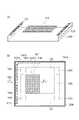
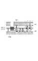
図1は、実施例1の固体撮像装置を示しており、図1(A)が固体撮像装置の斜視図であり、図1(B)は、図1(A)の固体撮像装置を光入射側から見た平面図である図1(A)に示すように、本実施例の固体撮像装置は、第1部材308と第2部材309とが貼り合わされた構造を有する第1部材308及び第2部材309はそれぞれが第1基板、第2基板を有している第1基板と第2基板との間には配線構造が配され、好ましくはこの配線構造は複数の配線層を含む以下、添え字でA、Bが振られている場合には、便宜上、第1部材308に配される構成にA、第2部材309に配される構成にBを振ることとする。 1 shows a solid-state imaging device of Example 1, FIG. 1A is a perspective view of the solid-state imaging device, and FIG. As shown in FIG. 1A, which is a plan view seen from the side, the solid-state imaging device of this embodiment has a structure in which a
第1部材308は、第2部材309よりも光入射側に配されている図1(B)において、図の左半分が第1部材308を示し、右半分は第1部材308が存在する部分を図示せず、第2部材309を示している第1部材308を図示していない右半分に関しても、左半分と同様にレイアウトすることができる。 The
図1において、301A、301Bは画素部である画素部301Aにはそれぞれが画素に対応する複数の光電変換部が配されている118はマイクロレンズであるマイクロレンズ118は各光電変換部に光を集光させる120は周辺回路である画素部301の信号を読み出すための種々の回路が配されている周辺回路120の主たる部分は第2部材309に配されるが、周辺回路120の一部を第1部材308に配することもできる。 In FIG. 1, 301A and 301B are pixel units, and the
312Aはパッド部であるパッド部312Aには複数のパッド313が配置されている複数のパッド313は、外部回路との信号等のやり取りを行う入力パッド、出力パッド(以下パッド)を含み得るパッド313は、例えば、配線構造の一部である導電パターンにより構成されうる通常、配線を構成する導電パターンは絶縁体により囲まれているが、パッドと外部回路とを電気的に接続するため、パッド上の絶縁体に開口100が配置されている。 A plurality of
そして、外部からの水分の浸入を抑制するためのシールリング150A、151A、152A、150Bが配置されている第1部材308には、第1部材308の最外周にシールリング150Aが配置され、シールリング150Aの内側であって、パッド部312Aと画素部301Aとの間にシールリング152Aが配置されるまた、パッド部312Aに配された各パッド313を囲むようにシールリング151Aが配置されているまた、第2部材309には最外周にシールリング150Bが配置されているつまり第1部材308はシールリング150A~152Aを含んで構成される第1シール部を有し、第2部材は150Bを含んで構成される第2シール部を有しているシールリングは主にそれぞれが配される部材に対して外部からの水分の浸入を抑制する後述するように、第1シール部の一部と第2シール部の一部とが接しているより具体的には第1シール部の第2部材309に対向する面と、前記第2シール部の第1部材308に対向する面とが接している。 The
ここでシールリングに関してさらに詳細に説明する本発明におけるシールリングは配置により4種類に分類でき、以下の実施例ではこれら4種類のシールリングを適宜組み合わせてシール部を構成する。 The seal rings in the present invention, which will be described in more detail here, can be classified into four types according to their arrangement, and in the following embodiments, these four types of seal rings are appropriately combined to constitute the seal portion.
まず一つ目の分類としては、それぞれの部材の最外周部に配されるシールリングである以下の実施例では符号150A、150Bが振られるシールリング150A、150Bは、各部材が有する、画素部、周辺回路部、パッド部よりも外側に配置される。 As the first classification, the
二つ目の分類としては、パッド部に配される各パッドの周囲に配され、該パッドを囲うように配されるシールリングである以下の実施例では符号151A、151Bが振られる。 The second classification is a seal ring arranged around each pad arranged in the pad section and arranged so as to surround the pad.
三つ目の分類としては、パッド部と画素部もしくはパッドと周辺回路部との間に配されるシールリングである以下の実施例では符号152A,152Bが振られる。 The third classification is seal rings arranged between a pad portion and a pixel portion or between a pad and a peripheral circuit portion, which are denoted by
四つ目の分類としては、それぞれの部材の貼り合わせ面に配された絶縁体により構成されたシール部であるこのシール部はパッシベーション層と兼ねることができる具体的にはSiN、SiONを用いることができるこれらはSiO2に比べて吸湿性が高いためシール機能も高い。 As a fourth classification, the sealing portion is a sealing portion made of an insulating material arranged on the bonding surfaces of the respective members. This sealing portion can also serve as a passivation layer. Specifically, SiN and SiON are used. Since these have higher hygroscopicity than SiO2, they also have a high sealing function.
本発明においては以上の四つに分類されたシールリングを適宜組み合わせてシール部を構成するより具体的には第1部材に配された第1シール部と第2部材に配された第2シール部とが互いに接してシール部を構成するシール機能を高めるためには、それぞれの部材に配されるシール部のうち、同じ分類のシールリングどうしを接触させるのがよい。 In the present invention, a seal portion is configured by appropriately combining seal rings classified into the above four types. More specifically, a first seal portion disposed on the first member and a second seal disposed on the second member. In order to improve the sealing function in which the members are in contact with each other to form a seal portion, it is preferable to bring the seal rings of the same classification among the seal portions arranged on the respective members into contact with each other.
次に、図2を用いて実施例1の固体撮像装置の等価回路図を説明する本実施例では、信号電荷が電子の場合について説明を行う図2の固体撮像装置300は、各々が光電変換部と光電変換部で生じた信号を処理もしくは該信号を読み出すための読み出し回路を有する複数の画素が配列された画素部301を有する更に、複数の画素からの信号を読み出すための周辺回路部302を有する周辺回路部302には図1の複数の周辺回路120が配される。 Next, in the present embodiment, in which the equivalent circuit diagram of the solid-state imaging device of the first embodiment will be described with reference to FIG. 2, the solid-
画素部301には、光電変換部303と、転送トランジスタ304と、増幅トランジスタ306と、リセットトランジスタ307が複数配置されている1つの光電変換部303を含む構成を画素とする本実施例の1つの画素は、光電変換部303と、転送トランジスタ304と、増幅トランジスタ306と、リセットトランジスタ307を含む転送トランジスタ304のソースは光電変換部303と接続しており、転送トランジスタ304のドレインは増幅トランジスタ306のゲートと接続しているこの増幅トランジスタ306のゲートと同一のノードをノード305とするリセットトランジスタ307のソースはノード305に接続し、ノード305の電位を任意の電位(例えば、リセット電位)に設定するリセットトランジスタ307のドレインにはリセット電圧が供給可能な構成となっているここで、増幅トランジスタ306はソースフォロア回路の一部であり、ノード305の電位に応じた信号を信号線RLに出力するノード305はフローティングディフュージョンを含んで構成することができる。 In the
周辺回路部302は複数の周辺回路が配されている例えば、画素部301のトランジスタのゲートへ制御信号を供給するための垂直走査回路VSRと、画素部301から出力された信号を増幅もしくは加算もしくはAD変換などの信号処理を行う読み出し回路RCを有するまた、周辺回路部302は、読み出し回路RCから信号を順次出力するためのパルスを供給する水平走査回路HSRを有する。 A
ここで、実施例1の固体撮像装置は、複数の光電変換部303は第1部材308に配されており、少なくとも画素の読み出し回路の一部、及び前記周辺回路が第2部材309に配されている具体的には光電変換部303と転送トランジスタ304とが第1部材308に配された画素部301Aとなり、それ以外の画素の構成要素が第2部材309に配された画素部であるなお、第1基板と第2基板の画素部の各トランジスタの配置は上記の構成に限られず、適宜、状況に合わせて変更可能である。 Here, in the solid-state imaging device of Example 1, the plurality of
接続部310は、第1基板に配された転送トランジスタ304のゲートと第2の部材に配された周辺回路120とを電気的に接続するノードである接続部310の具体的な構成については後述する。 The
光電変換部303にて生じた電荷は、転送トランジスタ304のドレイン、即ちノード305に読み出されるノード305は、第1部材308に配された構成と第2部材309に配された構成とを含み得る具体的に第1部材308に含まれる構成は、フローティングディフュージョン、及びフローティングディフュージョンと電気的に接続された第1配線構造の一部である第2部材309に含まれる構成は、リセットトランジスタ307のソース、増幅トランジスタ306のゲートと、及びこれらと第1配線構造の一部とを電気的に接続する第2配線構造の一部である。 The charge generated in the
このような構成によって、従来の1つの部材(即ち1つの基板)に画素部、周辺回路部の全てを配置する場合に比べて、光電変換部303の面積を大きくすることが可能となり感度を向上させることが可能となるまた、従来の構成に比べて、光電変換部の面積を同一とするならば、光電変換部303を多く設けることが可能となり、多画素化が可能となるそして、第1部材308の第1配線構造の一部と、第2部材309の第2配線構造の一部とにより、固体撮像装置の外部から侵入する水分を抑制するシール部を構成することができる。 With such a configuration, the area of the
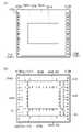
固体撮像装置の具体的な平面レイアウトを、図3の固体撮像装置の平面模式図を用いて説明する図3(A)は第1部材308の平面レイアウトを示すための上面図であり、図3(B)は第2部材309の平面レイアウトを示すための上面図である図1と図2と同様の機能を有する部分には同様の符号を付し詳細な説明は省略する。 FIG. 3A, which describes a specific planar layout of the solid-state imaging device using the schematic plan view of the solid-state imaging device in FIG. 3, is a top view showing the planar layout of the
図3(A)において、第1部材308には、複数の光電変換部303が配された画素部301Aと、複数のパッド313が配されたパッド部312Aとが配されている画素部301Aには、光電変換部303と転送トランジスタ304とが複数配されているまた、パッド313と平面的に同一位置に第2部材309との電気的接続のための接続部314Aが配されている接続部は配線構造に含まれる配線層と同一層で形成される導電パターンにより構成することができる。 In FIG. 3A, a
パッド313が入力パッドの場合には、パッド313に入力された信号もしくは電源電圧等が、接続部314Aを介して、第2の部材309の回路に供給されるパッド313が出力パッドの場合には、第2の部材309からの信号が接続部314Aを介して、パッド313に伝達されるなお、パッドには、配線層に配置された、外部回路が電気的に接続される電極パッドや半導体基板の一方の面から対向する他方の面に貫通する貫通電極と接続される電極パッドが含まれる。 When the
次に、図3(B)において、第2部材309には、画素部301Bと周辺回路部302Bとパッド部312Bとが配されているパッド部312Bにはパッドそのものが配されるわけではなく、第2部材309においてパッド313と電気的接続を取るための導電パターンが配される領域である画素部301Bには画素の読み出し回路を構成するトランジスタが配されており、例えば、図2における増幅トランジスタ306とリセットトランジスタ307が複数配置されている周辺回路部302には水平走査回路HSR、垂直走査回路VSR、読み出し回路RCが配されているパッド部312Bには、第1部材308に配された接続部314Aとの接続のための接続部314Bが配されている水平走査回路HSR、垂直走査回路VSR、読み出し回路RCと、夫々に対応する接続部314Bとは引き出し配線316を介して電気的に接続されている。 Next, in FIG. 3B, the
図3(A)及び図3(B)に示した平面レイアウトを有する第1部材308と第2部材309とは、図1で示した2つの部材が貼り合わせられた本実施例の固体撮像装置を個々に説明するための図である具体的には、画素部301Aと画素部301Bとが重なるように配置されるそして、接続部314Aと接続部314Bとが接続するなお、図3では、第2部材309の周辺回路部302Bに対応する第1部材308の領域を周辺回路部302Aとして示している周辺回路部302Aには走査回路の一部を配置してもよいし、回路素子を配さなくてもよいなお、第1部材308と第2部材309との役割の関係において、第1部材308は少なくとも光電変換部を有し、第2部材309は画素の読み出し回路あるいは周辺回路の少なくとも一部を有する。 The
次に、第1部材308のシール部について説明する以下の説明では、シール部は、第2部材309側から第1基板101に垂直に投影した場合における配置を示している第1部材308は、最外周部にシールリング150Aが配置されているここで最外周部とは、例えば、これよりも外側に回路素子が配されていない、もしくは導電パターンが配されていないことを示す更に、画素部301の周辺に配置された複数のパッド313には、個々のパッド313の周囲を囲むようにシールリング151Aが配置されているシールリング151Aは、パッド313と第1基板101に配された半導体領域との両者に電気的に接続させることができるなお、シールリング151Aが接続された半導体領域を含んで静電破壊保護回路を形成することが可能である静電破壊保護回路の一例としては保護ダイオードを用いることができるシールリング151Aにより、パッド開口部100からの水分浸入を抑制すると共に、外部からのノイズによる影響を抑制することができる。 Next, in the following description of the seal portion of the
そして、パッド部312Aと画素部301との間にはシールリング152Aが配置されているシールリング151Aを有する場合には、シールリング152Aは、シールリング151Aの画素部側の端部と、画素部301との間に配置されるのがよい好ましくは、シールリング152Aは画素部301の周囲を囲んでいる。 In the case where the
次に、第2部材309のシール部について説明する以下の説明における配置は、第1部材308側から第2基板121に垂直に投影した場合における配置を示している。 Next, the arrangement in the following description of the sealing portion of the
第2部材309のシールリング150Bは、第2部材309の最外周部に配されている各周辺回路120と各接続部314Bとを電気的に接続するための複数の引き出し配線316を有する場合は、複数の引き出し配線316よりも外側にシールリング150Bを配置するのがよい好ましくはシールリング150Bは、図示するように複数の引き出し配線316を囲むように配するのがよいまた、第2部材309のパッド部312Bにパッド313が配置される場合は、第1部材308のシールリング151Aと同様に配置されたシールリング151B(不図示)を設けてもよい。 When the
第1部材308と第2部材309とが貼り合わされた時の各部材におけるシールリングの位置関係は、重なる配置、重ならない配置のどちらでも可能である特に、パッシベーション層が配線構造の表面側に配置されている場合は、第1、第2部材の各シールリングは重ならなくても良いこれはパッシベーション層がシール部の一部を構成するためであるこの時パッシベーション層は配線構造の他の絶縁膜よりも吸湿性が高い材料で構成されるのがよい具体的な材料としては、窒素を含む材料であり、SiN、SiONなどを用いることができる。 The positional relationship of the seal rings in each member when the
また、第1部材308及び第2部材309の、導電体で構成したシールリングどうしを接するように配置することで防湿性が向上し、更には、信頼性が向上するまた、第1、第2部材の導電体で構成したシールリングどうしを接触させ連続的に一体化してシール部を構成することも考えられるこの場合は、第1部材308のウエハと第2部材309のウエハとを結合させた後でダイシングする時に、チッピングの範囲の拡大をシールリングで抑えることができる更には、歩留まりや信頼性が向上する。 In addition, by arranging the seal rings of the
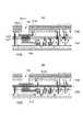
図4は、図1のX-X’線での断面模式図であり、図2及び図3に示した回路、平面レイアウトを有する固体撮像装置を説明する図である図4では、図1~図3と同一の構成には同一の符号を付し詳細な説明を省略する。 FIG. 4 is a schematic cross-sectional view taken along line XX' of FIG. The same components as those in FIG. 3 are denoted by the same reference numerals, and detailed description thereof will be omitted.
本実施例の固体撮像装置は、第1基板と、第2基板と、第1基板と第2基板の間に配置された配線構造と、を有する第1基板は好ましくは半導体基板であり、第1の部材308に含まれる第2基板は好ましくは半導体基板であり、第2の部材309に含まれる。 The solid-state imaging device of this embodiment has a first substrate, a second substrate, and a wiring structure arranged between the first substrate and the second substrate. A second substrate included in one
配線構造は、好ましくは、複数の配線層が絶縁層を介して積層された構造を有しているまた、配線構造は、第1の部材308が第1の配線構造を有し第2の部材309が第2配線構造を有して構成されてもよいこの場合は第1配線構造及び第2配線構造の両者が複数の配線層が絶縁層を介して積層された構造を有しているとよいもしくは第1及び第2の部材の一方のみが配線構造を有して構成されてもよい。 The wiring structure preferably has a structure in which a plurality of wiring layers are laminated with insulating layers interposed therebetween. 309 may have a second wiring structure. Alternatively, only one of the first and second members may be configured with a wiring structure.
第1部材308は、絶縁層と配線層とを少なくとも有する第1配線構造と第1基板101とを有する第1基板101は例えば半導体基板であり、主面102と裏面103とを有する本実施例における第1基板101はn型のシリコン半導体基板である第1基板の主面102には光電変換部303が配置されている第1配線構造は、層間絶縁膜104~106と、ゲート電極やゲート配線を含むゲート電極層107を含む更に、複数の配線を含む配線層109、111と、複数のコンタクトプラグあるいはビアプラグを含むプラグ層108、110とを有する層間絶縁膜106は、第1配線構造の最表面に配置されたパッシベーション層であるここではパッシベーション層としてSiNを有する絶縁膜を用いている。 The
第1基板101には、光電変換部303を構成するn型半導体領域112と、転送トランジスタのドレインつまりフローティングディフュージョンであるn型半導体領域114が配されている更に、素子分離構造119が配されている素子分離構造119は絶縁体を用いて構成してもよいし、絶縁体を用いずにPN接合分離を用いてもよいもしくは両者を組み合わせて用いてもよい転送トランジスタ304はn型半導体領域112とn型半導体領域114とゲート電極層107に含まれるゲート電極113とを含んで構成されるここで、n型半導体領域112の電荷は、ゲート電極113に供給される駆動パルスによって、n型半導体領域114に転送されるn型半導体領域114に転送された電荷に基づく電位はプラグ層108、配線層109、プラグ層110、配線層111を介して、第2部材309へと伝達される配線層111に含まれる導電パターンの一部が接続部311Aを構成するなお、光電変換部303は更に受光面側にp型半導体領域を有する埋込みフォトダイオードであってもよく、フォトゲートであってもよく、適宜変更可能である。 The
画素部301Aの第1基板101の裏面103側には、平坦化層115、複数のカラーフィルタを含むカラーフィルタ層116、平坦化層117、複数のマイクロレンズを含むマイクロレンズ層118がこの順に配置されている図4において、複数のカラーフィルタ及び複数のマイクロレンズはそれぞれが1つの光電変換部に対応して、すなわち画素毎に配置されているが、複数画素に対して1つずつ設けられていてもよい本実施例の固体撮像装置は、このマイクロレンズ層118側から光が入射し光電変換部が受光する、所謂裏面照射型の固体撮像装置である。 A
第1部材308のパッド部312Aには、パッド313と、パッド313上を露出する開口部100とが配されているまた、パッド313と電気的に接続された接続部314Aが配置されている接続部314Aは配線層111に含まれる導電パターンにより構成される。 The
第1部材308の第1配線構造の一部でシールリングが構成されているシールリング150A、151A、152Aは、配線層やプラグ層と同一工程で形成される導電パターンで形成することができる。 The seal rings 150A, 151A, and 152A, which are part of the first wiring structure of the
シールリング150Aを第2部材309側から第1基板101に垂直に投影した領域は、第1部材の最外周に配されるしたがって第1基板の複数の光電変換部が配された領域、つまり画素部301Aはシールリング150Aを投影した領域の内側に配されるシールリング150Aは、画素部301A及びパッド部312Aの両者の外側に設けられ、それらの全体を囲んでいる。 A region obtained by vertically projecting the
シールリング152Aを第2部材309側から第1基板101に垂直に投影した領域は、画素部302とパッド部312Aとの間に配される更に好ましくは、シールリング152Aは画素部301Aを囲んでいる。 A region where the
この配置関係は、図4と図3(A)とを参照すればより容易に理解されるそして、シールリング150A,152Aは第1基板101の主面102から層間絶縁膜106の第1基板101とは反対側の表面まで配置されている。言い換えると、シールリング150A,152Aは、半導体基板からパッシベーション膜として機能する層間絶縁膜106の第2部材309と接する面まで導電体が連続して配された構造である。 This positional relationship can be more easily understood with reference to FIGS. is arranged up to the surface on the opposite side. In other words, the seal rings 150A and 152A have a structure in which a conductor is continuously arranged from the semiconductor substrate to the surface of the
本実施例においては、更に、パッド部312Aに配された各パッド313周囲にシールリング151Aを有する。 In this embodiment, a
シールリング150Aと152Aの少なくとも一方を有していれば、固体撮像装置の端部、およびパッド開口部から固体撮像装置内の素子への水分の浸入経路が狭くなるため、防湿性が確保できる。 With at least one of the seal rings 150A and 152A, moisture resistance can be ensured because the passage of moisture from the edge of the solid-state imaging device and the pad opening to the elements in the solid-state imaging device is narrowed.
また各シールリングは、第1基板101内に配置された、例えば、第1基板101と同じ導電型である半導体領域114´、112´を介して基板電位が供給されているこのような構成とすると、外来ノイズの影響を抑制することができる。 Each seal ring is supplied with a substrate potential via semiconductor regions 114' and 112', which are arranged in the
第2部材309は、第2配線構造と第2基板121とを有する第2基板121は例えば半導体基板であり、主面122と裏面123とを有する第2基板の主面122にはトランジスタが配置される第2配線構造は、層間絶縁膜124~127と、ゲート電極や配線を含むゲート電極層128と、複数の配線を含む配線層130、132、134と、複数のコンタクトあるいはビアを含むプラグ層129、131、133とを有する更に、最上配線層である配線層134に含まれる導電パターンは、第1部材308との電気的接続部を含む層間絶縁膜127は、第2配線構造の最表面に配置されたパッシベーション層であるここではパッシベーション層として窒素を含むSiN,SiONを用いることができる。 The
第2基板121の画素部301Bには、増幅トランジスタ306のチャネルを提供するp型の半導体領域135と、増幅トランジスタ306のn型のソース領域、ドレイン領域138と、素子分離構造136とが配されている増幅トランジスタ306は、ゲート電極層128に含まれるゲート電極137と、ソース領域、ドレイン領域138とで構成されるここで、第1部材308の接続部311Aと増幅トランジスタのゲート電極137とは、配線層134、プラグ層133、配線層132、プラグ層131、配線層130、プラグ層129とを介して電気的に接続されるここで、図2のノード305は、図4のn型半導体領域114と、配線層109、111、134、132、130の配線と、プラグ層108、110、133、131、129のコンタクトプラグあるいはビアプラグと、ゲート電極137と、を含んで構成される画素部301Bの他の回路(例えば、リセットトランジスタ)は不図示である。 In the
第2部材309の周辺回路部302には、水平走査回路HSRや垂直走査回路VSRが配置されている図4では、周辺回路部302に含まれる任意の回路のn型のトランジスタとp型のトランジスタを示しているn型トランジスタは、ゲート電極層128に含まれるゲート電極140とP型の半導体領域139に配されたn型のソース領域、ドレイン領域141とを含んで構成されているそして、p型のトランジスタは、ゲート電極層128に含まれるゲート電極143とn型の半導体領域142に配されたp型のソース領域、ドレイン領域144とを含んで構成されている。 A horizontal scanning circuit HSR and a vertical scanning circuit VSR are arranged in the
シールリング150Bは、第2配線構造を構成する配線層やプラグ層の一部を用いて構成することができるシールリング150Bを第1部材308側から第2基板121に垂直に投影した領域は第2部材309の最外周部に配されるもしくは各種周辺回路を含む周辺回路部302の外側に配置されているこの配置関係は、図4と図3(B)とを参照すればより容易に理解されるそして、シールリング150Bは第2基板121の主面122からパッシベーション膜として機能する層間絶縁膜127の第2基板121とは反対側の表面まで配置されている。言い換えると、シールリング150Bは、半導体基板からパッシベーション膜として機能する層間絶縁膜106の第1部材308と接する面まで導電体が連続して配された構造である。 The
図4に示したようにシールリング150Aと150Bとは互いに接しているより具体的には、シールリング150Aの第2部材309側の最表面を構成する配線層111の導電パターンと、シールリング150Bの第1部材308側の最表面を構成する配線層134の導電パターンとが接している。 As shown in FIG. 4, the seal rings 150A and 150B are in contact with each other. is in contact with the conductive pattern of the
シールリング150Bは、第2基板121内に配置された、第2基板121と同じ導電型の半導体領域138´、139´を介して基板電位が供給されているそのため、シールリング150Bによって、外来ノイズの影響を抑制することができる。 The
以上のような、第1基板101の主面102と第2基板121の主面122とが向かい合って、第1部材308と第2部材309とが貼り合わされ(対向配置)、固体撮像装置を構成している。 As described above, the
このような構成によって、第1部材308の画素部301Aや、第2部材309の画素部301Bと周辺回路部302Bとを含む素子領域への水分の浸入を抑制することが可能となる。 With such a configuration, it is possible to suppress penetration of moisture into the element region including the
また、第1部材308の裏面側にパッド313の露出面が配置されることにより、外部回路からパッド313への電気的接続が容易となり、接続不良が抑制される。 In addition, by arranging the exposed surface of the
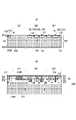
ここで、図4の固体撮像装置の変形例を示す断面模式図の図5(A)及び図5(B)を用いて説明する図5(A)の固体撮像装置が、図4の固体撮像装置と異なる点は、第1及び第2配線構造の最表面にパッシベーション層としての機能がSiNなどより小さい絶縁層106’が配置されている構成であるその他、図4の構成と同様の機能を有する部分には同様の符号を付し詳細な説明は省略する。 Here, the solid-state imaging device of FIG. 5A, which will be described with reference to FIGS. The difference from the device is that an insulating
また、図5(A)の構成においてはシールリング152Aを設けていないこの場合であってもシールリング151Aにより一定の防湿性を確保することが可能であるこれに対してシールリング150A、150Bは配置されているこの構成により、パッシベーション層が配置されていないことによる第1、第2部材308、309の各最表面からの水分などの浸入の可能性を抑制することができる。 In addition, in the configuration of FIG. 5A, even in this case where the
次に、図5(B)の固体撮像装置を説明する図5(B)の固体撮像装置が図4の固体撮像装置と異なる点は、シールリング150A、151Aを有さない点であるそして、パッシベーション層として機能する層間絶縁膜106´、127´が第1、第2部材308、309の各最表面に配置されているシールリング152A、150Bは配置されているこのような構造の場合には、パッド313と第2部材309との電気的接続を取るための、第1部材308の導電パターン、第2部材309の導電パターンもシール部の一部を構成しているこの構成により、パッド開口100での第1配線構造の断面からの水分などの浸入を抑制することができる各シールリングは、配線構造に含まれる配線層とプラグ層と同じ材料で構成された導電パターンの積層構造を有する。 Next, the solid-state imaging device of FIG. 5B, which explains the solid-state imaging device of FIG. 5B, differs from the solid-state imaging device of FIG. 4 in that it does not have
次に、本実施例の図4の固体撮像装置の製造方法を、図6~8を用いて説明する図6は第1部材308の製造工程を示す断面模式図であり、図7は第2部材309の製造工程を示す断面模式図であり、図8は第1部材308と第2部材309とを接合した後の製造工程を示す断面模式図である。 Next, a method for manufacturing the solid-state imaging device shown in FIG. 4 of this embodiment will be described with reference to FIGS. 6 to 8. FIG. FIG. 8 is a schematic cross-sectional view showing the manufacturing process of the
図4の第1部材308の製造工程を図6を用いて説明する図6においては、後に図4の第1部材308になる構成を308’とし、図4の画素部301、周辺回路部302、パッド部312、回路素子になる領域を301’、302’、312’としているそして、シールリング150A、151A、152Aになる領域をシールリング150A’、151A’、152A’としている。 In FIG. 6, which explains the manufacturing process of the
まず、半導体基板401を準備し、半導体基板401に素子を形成する半導体基板401は主面402と裏面403を有し、その厚みはD3である半導体基板401を構成する主たる材料はシリコンである。 First, a
半導体基板401に、素子分離構造119を形成する素子分離構造119は、絶縁体を有し、例えばLOCOSやSTI構造であるもしくはPN接合分離、絶縁体とPN接合分離の両者を有する構造としてもよいそして、半導体基板401にP型及びN型のウエルとして機能する半導体領域(不図示)を形成するその後、光電変換部を構成するn型半導体領域112、114を形成するまた、シールリングを構成する導電体に電気的に接続されるn型半導体領域112’、114’を形成するn型半導体領域112’、114’は基板と同じ導電型とすることができる。 The
次にゲート電極層107を形成するゲート電極層107は例えば、ポリシリコンで形成され、ゲート電極のみではなく配線をも含みうるここで、ゲート電極、素子分離及び半導体領域の形成方法については、一般的な半導体プロセスで形成可能であり、詳細な説明は省略する以上によって、図6(A)の構成が得られる。 Next, the
次に、半導体基板401の主面上に第1配線構造321を形成する第1配線構造321は、層間絶縁膜104、105、106と、プラグ層108、110と、配線層109、111とを有するここで、層間絶縁膜はシリコン酸化膜やシリコン窒化膜、あるいは有機樹脂等で形成され、配線層はアルミニウムを主成分とする配線や銅を主成分とする導電体からなる最表面の層間絶縁膜である層間絶縁膜106は、パッシベーション膜としてシリコン酸窒化膜やシリコン窒化膜で形成されうるコンタクトプラグは例えばタングステンで形成され、ビアプラグはタングステンで形成される配線材料として銅を用いた場合にはいわゆるダマシン構造として、ビアプラグを構成する材料として銅を主成分とすることができるここで、配線層111を構成する導電パターンにより接続部314Aが構成される導電パターンの材料としては銅を主成分とすることができるまた、配線層109に含まれる導電パターンによりパッド313が構成されるパッドの材料はアルミニウムを主成分とするこれら配線層、プラグ層、層間絶縁膜の製造方法については、一般的な半導体プロセスで形成可能であり、詳細な説明は省略する以上によって、図6(B)の構成が得られる。 Next, the
次に、図4の第2部材309の製造工程を、図7を用いて説明する図7においては、後に図4の第2部材309となる構成を309’とし、図4の画素部301B、周辺回路部302B、パッド部312Bになる領域を301’、302’、312’としているそして、シールリング150Bになる領域を150B´としている。 Next, in FIG. 7, the manufacturing process of the
まず、半導体基板404を準備し、半導体基板404に素子を形成する半導体基板404は主面405と裏面406を有し、その厚みはD4であるそして、半導体基板404にLOCOSやSTI構造を用いて素子分離構造136を形成するまた、半導体基板404にp型のウエルとして機能するP型の半導体領域135、139やn型のウエルとして機能するn型の半導体領域142を形成するその後、トランジスタを構成するソース領域、ドレイン領域となりうるn型半導体領域138、141、及びp型半導体領域144や、保護ダイオードを構成する半導体領域を形成するまた、シールリングを構成する導電体に電気的に接続されるn型半導体領域138’、139’を形成するn型半導体領域138’、139’は基板と同じ導電型とすることができるそして、トランジスタのゲート電極137、140、143及び配線(抵抗)を含むゲート電極層128をポリシリコン層の堆積及びパターニングによって形成するここで、ゲート電極、素子分離及び半導体領域の形成方法については、一般的な半導体プロセスで形成可能であり、詳細な説明は省略する以上によって、図7(A)の構成が得られる。 First, a
次に、半導体基板404の主面上に第2配線構造322を形成する配線構造は、層間絶縁膜124~127と、プラグ層129、131、133と、配線層130、132、134とを有するここで、層間絶縁膜はシリコン酸化膜であるシリコン窒化膜、あるいは有機樹脂等で形成され、配線層はアルミニウムを主成分とする配線や銅を主成分とする配線からなるここで、配線層134の導電パターンにより接続部314Bが構成され、銅を主成分とする材料から構成される最表面の層間絶縁膜である層間絶縁膜106は、パッシベーション膜として機能するようにシリコン酸窒化膜やシリコン窒化膜で形成されるこれら配線層、プラグ層、層間絶縁膜の製造方法については、一般的な半導体プロセスで形成可能であり、詳細な説明は省略する以上によって、図7(B)の構成が得られる。 Next, the wiring structure forming the
次に、図6(B)及び図7(B)に示した第1部材308’と第2部材309’とを、互いの半導体基板の主面402及び主面405とが向かい合うように貼り合わせるつまり、第1部材308’の配線構造の最上面と第2部材309’の配線構造の最上面とが接合されるここで、第1接続部311及び314及び801は銅を主成分とする導電パターンから構成されているため、貼り合わせの際は銅の金属接合によって行うことが可能であるシールリング150Aのシールリング150Bと直接接する最表面の導電パターンとシールリング151Bのシールリング150Aと直接接する最表面の導電パターンとが接続部152を構成するまた、図6(B)で示した第1配線構造321と図7(B)で示した第2配線構造322とにより配線構造320が形成される。 Next, the first member 308' and the second member 309' shown in FIGS. 6B and 7B are pasted together so that the
第1部材308’と第2部材309’とが接合された後に、第1部材308’の半導体基板401の裏面403側を除去して厚みを減少させてもよいすなわち第1部材308’を薄膜化するまた、第2部材309’の半導体基板404の裏面406側を除去して厚みを減少させてもよいすなわち第2部材309’を薄膜化するなお、本実施例の薄膜化は、CMPやエッチングによって行うことが可能であるそして、半導体基板401は半導体基板101となり、厚みがD3からD1(D1<D3)となる(図8(A))このように半導体基板401を薄膜化し半導体基板101とすることで、後に入射光が光電変換部に効率良く入射することを可能にする半導体基板404は半導体基板121となり、厚みがD4からD2(D2<D4)となる(図8(A))また、この時、半導体基板101の厚みD1<半導体基板121の厚みD2となる第2部材309’の薄膜化を行わない場合は、半導体基板101の厚みD1<半導体基板404の厚みD4となる。 After the first member 308' and the second member 309' are joined, the thickness of the first member 308' may be reduced by removing the
次に、半導体基板101の裏面408に、樹脂からなる平坦化層115、カラーフィルタ層116、樹脂からなる平坦化層117、マイクロレンズ層118をこの順に形成するこれら平坦化層、カラーフィルタ層、マイクロレンズ層の製造方法については、一般的な半導体プロセスで形成可能であり、詳細な説明は省略するここでマイクロレンズ層はパッド部となる312’の領域まで形成されていてもよい以上の工程によって、図8(B)の構成が得られる。 Next, on the
そして、パッド313表面を露出するための開口100を形成するここでは、フォトリソグラフィ技術を用いてマイクロレンズ層118の上に任意の開口を有するフォトレジストマスクを設けるそして、ドライエッチング技術を用いて、マイクロレンズ層118、平坦化層117、カラーフィルタ層116、平坦化層115、半導体基板101及び層間絶縁膜104’を除去し、パッド313を露出させる開口100を形成するそして、マイクロレンズ層118、平坦化層117、115、カラーフィルタ層116、半導体基板101及び層間絶縁膜104が形成される以上の工程によって、図8(C)の構成、すなわち図4と同じ構成が得られる。 Then, an
以上のように、シールリング150A、151A、152A、150Bは配線構造の配線と同一工程で形成可能であるなお、エッチングの際には、パッド313をエッチングストッパとして機能させることが可能である。 As described above, the seal rings 150A, 151A, 152A, and 150B can be formed in the same process as the wiring of the wiring structure. During etching, the
本発明は本実施例の製造方法において説明した工程に限定されるものではなく、工程順が変更されていてもよいまた、第2部材309は第1部材308に引き続いて形成してもよいし、並行して形成してもよい更には、第1部材308と第2部材309とを購入し、貼り合わせて形成することも可能であるなお、半導体基板401、402にはSOI基板を適用することも可能である。 The present invention is not limited to the steps described in the manufacturing method of this embodiment, and the order of the steps may be changed. Further, it is also possible to purchase the
(実施例2)
本発明の実施例2について、図9を用いて説明する図9(A)、図9(B)及び図9(C)は固体撮像装置の断面模式図であり、それぞれ図4で示した固体撮像装置の変形例を示す断面図である図9において図4と同様の構成については同一の符号を付し、詳細な説明を省略する。(Example 2)
9(A), 9(B), and 9(C) for explaining the second embodiment of the present invention with reference to FIG. 9 are schematic cross-sectional views of the solid-state imaging device. In FIG. 9, which is a cross-sectional view showing a modified example of the imaging apparatus, the same reference numerals are given to the same components as in FIG. 4, and detailed description thereof will be omitted.
本実施例において、実施例1と異なる点は、パッド313から第2部材への電気経路である実施例1においては第1部材に配されたパッド313を第2部材方向に垂直投影した領域内にプラグ、配線を配していたそして、第2部材の下層の配線層まで電気経路を形成した後、第2部材の回路素子との信号の受け取りが可能なように電気的接続を行なっていた。 In the present embodiment, the difference from the first embodiment is that the electric path from the
これに対して本実施例においては、第1部材内でパッド313から周辺回路部まで電気経路を設けた後、プラグ等を介して第2部材との電気的接続を行なっている。 On the other hand, in this embodiment, after providing an electric path from the
図9(A)に示すように、第1部材808において、パッド313から周辺回路部まで水平方向に延伸した引き出し配線316を有するまた、第2部材809は第1部材808の引き出し配線316により水平方向に延伸された領域に接続部を有するシールリング150A、151A、152A、150Bは、実施例1と同様の構成であるなお、図9(A)の固体撮像装置はシールリング151Aを配することにより、シールリング150Aと152Aの少なくとも一方が配置されていれば良いしかし、150Aと152Aが連続的に配されている構成は実施例1で説明したように防湿効果やチッピング対策として有効であるまたパッド313は第2部材809の主面122よりも第1部材808側に配されていればどのような位置に配置されていてもよい。 As shown in FIG. 9A, the
次に、図9(B)について説明する図9(B)の図9(A)の固体撮像装置と異なる点は、パッシベーション層を有していない点である配線構造の最表面にパッシベーション層としての機能がSiNなどより小さい絶縁層106’が配置されているこの場合は、シールリング151Aを有しているため、図9(B)で示すようにシールリング152Aは必ずしも必要ではないが、シールリング150A、151Bは配置され、各々の最表面を構成する導電パターンどうしが接しているこの構成により、パッシベーション層が配置されていないことによる第1、第2部材の各最表面からの水分などの浸入を抑制することができるまた、第2部材809のシールリング150Bは、パッド部の内側の周辺回路部より外側で、パッド部より外側の外周部までの間に配置すればよい図9(B)の固体撮像装置では、第2部材の最外周にシールリング150Bを配置して図9(A)と同様な効果を得ている。 Next, FIG. 9B, which will be explained with reference to FIG. 9B, differs from the solid-state imaging device of FIG. 9A in that it does not have a passivation layer. In this case, since the insulating
次に、図9(C)の固体撮像装置の説明をする図9(C)の固体撮像装置が図9(A)の固体撮像装置と異なる点は、シールリング151Aを有さずに、パッシベーション層が第1、第2部材の各最表面に配置されている構成であるこの場合は、シールリング150A、150Bは必ずしも必要ではないが、シールリング152Aは配置されるまたこのような構成はパッシベーション層がシールリングの一部を構成しているともいえる。 Next, the solid-state imaging device of FIG. 9C, which explains the solid-state imaging device of FIG. 9C, differs from the solid-state imaging device of FIG. The layers are arranged on the outermost surfaces of the first and second members. In this case, the seal rings 150A and 150B are not necessarily required, but the
この構成により、パッド部の開口での配線構造の断面からの水分などの浸入を抑制することができる。 With this configuration, it is possible to suppress penetration of moisture or the like from the cross section of the wiring structure at the opening of the pad portion.
(実施例3)
本発明の実施例3について、図10、図11を用いて説明する図10(A)、図10(B)及び図10(C)は固体撮像装置の断面模式図であり、それぞれ図4で示した固体撮像装置の変形例を示す断面図である図11は図10の固体撮像装置の更なる変形例である図10、図11において図4と同様の構成については同一の符号を付し、説明を省略する。(Example 3)
10(A), 10(B), and 10(C) for explaining the third embodiment of the present invention with reference to FIGS. 10 and 11 are schematic cross-sectional views of the solid-state imaging device. FIG. 11 is a cross-sectional view showing a modification of the solid-state imaging device shown in FIG. 10, which is a further modification of the solid-state imaging device shown in FIG. , the description is omitted.
本実施例において、実施例1と異なる構成はパッドの配置である。 In this embodiment, the configuration different from that of the first embodiment is the arrangement of the pads.
図10(A)が図4の固体撮像装置と異なる点はパッド1013を構成する導電パターンが第2部材909に配されている点であるそして第1部材908のパッド部に対応する第1部材908の一部が貫通されているまた、第2部材909は、パッド313から水平方向への引き回しを行う引き出し配線316を有するシールリングは、実施例1と同様の構成を用いることができるまた、外部ノイズの影響も抑制できるなお、図10(A)の固体撮像装置はシールリング151Aを有するため、シールリング150Aと152Aの少なくとも一方が配置されていれば良い150Aと150Bとが全周で接続されている構成は実施例1で説明したように防湿効果やチッピング対策として有効である。 10A differs from the solid-state imaging device of FIG. 4 in that the conductive pattern forming the pad 1013 is arranged on the
次に、図10(B)が図10(A)の固体撮像装置と異なる点は、パッシベーション層を有していない点である配線構造の最表面にパッシベーション層としての機能がSiNなどより小さい絶縁層106’が配置されている図9(B)と同様の趣旨の実施形態であるこの場合は、シールリング151A、151Bを有しているため、図9(B)で示すようなシールリング152Aは必ずしも必要ではないが、シールリング150A、150Bは配置するこの構成により、パッシベーション層が配置されていないことによる第1、第2部材の各最表面からの水分などの浸入の可能性を抑制することができるまた、第2部材809のシールリングは、パッド部の内側の周辺回路部より外側で、パッド部より外側の外周部までの間に配置すればよい図10(B)の固体撮像装置では、外周部にシールリング150Aを配置して図10(A)と同様な効果を得ることができる。 Next, FIG. 10B differs from the solid-state imaging device of FIG. 10A in that it does not have a passivation layer. In this case, which is an embodiment similar to FIG. 9(B) in which the
次に図10(C)の固体撮像装置について説明する図10(c)が図10(A)の固体撮像装置と異なる点は、シールリング151Aを有さずに、パッシベーション層が第1、第2部材の各最表面に配置されている構成である図9(c)の構成と同趣旨の実施形態であるこの場合は、シールリング150Aは必ずしも必要ではないが、シールリング152A、150B、151Bは配置するこの構成により、パッド部の開口での配線構造の断面からの水分などの浸入を抑制することができるなお、シールリング150A、150Bとは、全周にわたって接続されていなくても良い。 Next, FIG. 10C, which describes the solid-state imaging device of FIG. 10C, differs from the solid-state imaging device of FIG. In this case, the
図11は、図10の固体撮像装置の変形例で、第2部材1009にパッド313が配されているそしてパッド313に対して第2基板の裏面側から第2基板を貫通する貫通電極317を有するパッド313は、配線層と同じ導電パターンで形成され、半導体基板の一方の面から対向する他方の面に貫通する貫通電極317と接続される電極パッドであるそして、他の実施例で説明したパッド部のシールリング151Aを形成する必要がなく、シールリング150A、150Bを有していればよい固体撮像装置の裏面で他の回路基板と接続できるため、固体撮像装置の小型化が実現できる。 FIG. 11 shows a modification of the solid-state imaging device of FIG. 10, in which a
(実施例4)
本発明の実施例4について、図12を用いて説明する図12(A)、図12(B)及び図12(C)は固体撮像装置の断面模式図であり、それぞれ図4で示した固体撮像装置の変形例を示す断面図である図12において図4と同様の構成については同一の符号を付し、説明を省略する。(Example 4)
12(A), 12(B), and 12(C) for explaining the fourth embodiment of the present invention with reference to FIG. 12 are schematic cross-sectional views of the solid-state imaging device. In FIG. 12, which is a cross-sectional view showing a modified example of the imaging device, the same reference numerals are given to the same components as in FIG. 4, and the description thereof will be omitted.
本実施例において、実施例1と異なる構成は、引き出し配線316とパッド部の配置であるなお、図12は図10で示した固体撮像装置と同様にワイヤーボンディング用に、パッド上の第1部材1108、第2部材1109の一部が除去されている。 In the present embodiment, the configuration different from that of the first embodiment is the layout of the
図12(A)が図4の固体撮像装置と異なる点は、第1部材1108のパッド部に対応する部分が除去されており、第2部材1109にパッド313を有する点であるまた、第2部材1109のパッド313と周辺回路部とを電気的に接続するために第1部材1108に配置された引き出し配線316を有する。 FIG. 12A differs from the solid-state imaging device of FIG. 4 in that the portion corresponding to the pad portion of the
第1部材1108に第1シール部として、シールリング150A、151A、152Aが配されるそして、第2部材1109に第2シール部として150B、151B、152Bが配されるこれまでの実施例と同様に第1シール部、第2シール部に外部からのノイズの影響を抑制する機能を持たせてもよいまた、第2部材1109のシールリング152Bはパッド部と周辺回路との間に配置される更に、シールリング152Bは、第1部材1108側から第2部材1109の第2基板に垂直に投影した場合に、周辺回路部の周囲を囲むように配置されているのがよいなお、図12(A)の固体撮像装置はシールリング151Aを有するため、シールリング150Aと152Aの少なくとも一方が配置されていれば良いそして、シールリング151Bを有するため、シールリング150Bと152Bの少なくとも一方が配置されていれば良い。 The
次に、図12(B)の固体撮像装置の説明をする図12(B)の構成が図12(A)の固体撮像装置と異なる点は、パッシベーション層を有していない点である配線構造の最表面にパッシベーション層としての機能がSiNなどより小さい絶縁層106’が配置されている構成である図9(B)、図10(B)と同趣旨の実施形態であるこの場合は、シールリング151A、151Bを有しているため、図12(B)で示すようにシールリング152Aは必ずしも必要ではないが、シールリング150Aは配置する。 Next, the configuration of FIG. 12B for explaining the solid-state imaging device of FIG. 12B differs from the solid-state imaging device of FIG. 12A in that it does not have a passivation layer. 9(B) and 10(B), in which an insulating
この構成により、パッシベーション層が配置されていなくても第1、第2部材の各最表面からの水分などの浸入の可能性を抑制することができるなお、シールリング150B、151Bが配置されていればシールリング152Bは必ずしも必要ではないが、シールリング152Bを配置すればより防湿性が向上する。 With this configuration, even if the passivation layer is not arranged, the possibility of entry of moisture or the like from the outermost surfaces of the first and second members can be suppressed. Although the
次に図12(C)の固体撮像装置の説明を行う図12(C)の構成が図12(A)の固体撮像装置と異なる点は、配線構造が、シールリング151Aを有さずに、パッシベーション層が第1、第2部材の各最表面に配置されている構成であるシールリング150Aとシールリング152Aは配置されているそして、シールリング152Bも配置されているこの構成により、パッド部の開口での配線構造の断面からの水分などの浸入を抑制することができるなお、パッド313が第2部材の最表面に配置されている場合は、シールリング152Bは配置されていなくても良いが、配置すれば、より防湿性が向上する。 Next, the solid-state imaging device shown in FIG. 12C is described. The configuration shown in FIG. 12C differs from the solid-state imaging device shown in FIG. The
以上、第1部材と第2部材とを重ねて接続した固体撮像装置の説明を行ったが、第1部材と第2部材のシールリング150A、150Bが電気的に接続され、且つ、各々が基板に配された半導体領域と接続される場合にはそれら半導体領域は同じ導電型がよい。 The solid-state imaging device in which the first member and the second member are stacked and connected has been described above. If the semiconductor regions are connected to each other, the semiconductor regions should preferably be of the same conductivity type.
第1部材のシールリングと第2部材のシールリングを接続せず、独立して配置する場合は、異なる導電型の半導体基板を用いることが可能であるこの独立して配置する構成は、第1部材、第2部材の半導体基板が同じ導電型であっても異なる導電型であっても、どちらかの部材にノイズが混入した場合に、もう一方の基板はその影響を受けにくいという効果を有する。 When the seal ring of the first member and the seal ring of the second member are arranged independently without being connected, semiconductor substrates of different conductivity types can be used. Even if the semiconductor substrates of the member and the second member have the same conductivity type or different conductivity types, when noise enters one of the members, the other substrate is less affected by the noise. .
(実施例5)
図13を用いて実施例5の固体撮像装置に関して説明する実施例5の固体撮像装置の実施例1~4の固体撮像装置と異なる点は、第1部材と第2部材のシール部において、導電体で構成されたシールリングどうしは接触しておらず、第1部材、第2部材の最表面に配されたパッシベーション層が互いに接している点である。(Example 5)
The solid-state imaging device according to the fifth embodiment, which will be described with reference to FIG. The point is that the seal rings composed of bodies are not in contact with each other, and the passivation layers arranged on the outermost surfaces of the first member and the second member are in contact with each other.
第1部材1308は導電体により構成されたシールリング152Aを有している第2部材1309は導電体により構成されたシールリング150Bを有しているシールリング152Aと150Bとは水平方向にオフセットして配されており、互いの最表面を構成する導電パターンどうしが接していない。しかしながら最表面を吸湿性の高いパッシベーション層1301A,1301Bを配することにより、シール特性を維持している。 The first member 1308 has a
以下、上記の各実施形態に係る固体撮像装置の応用例として、固体撮像装置が組み込まれた撮像システムについて例示的に説明する撮像システムには、撮影を主目的とするカメラなどの装置のみならず、撮影機能を補助的に備える装置(例えば、パーソナルコンピュータ、携帯端末)も含まれる例えば、カメラは、本発明に係る固体撮像装置と、固体撮像装置から出力される信号を処理する処理部とを含むこの処理部とは、例えば、A/D変換器、及びA/D変換器から出力されるデジタルデータを処理するプロセッサを含みうる。 As application examples of the solid-state imaging devices according to the above-described embodiments, an imaging system incorporating the solid-state imaging device will be exemplified below. , and also include devices (e.g., personal computers, mobile terminals) that have an auxiliary imaging function. The processing unit may include, for example, an A/D converter and a processor that processes digital data output from the A/D converter.
以上述べてきたように、本発明の固体撮像装置によれば、光電変換部や周辺回路部への水分の浸入が抑制可能であるまた、本発明の製造方法によれば、第1部材と第2部材との接続部による結合と同時にシールリングの結合を同時に行うことができるため、製造工程に必要な時間を増やすことなく防湿性向上やチッピング抑制が可能となる。 As described above, according to the solid-state imaging device of the present invention, it is possible to suppress the intrusion of moisture into the photoelectric conversion portion and the peripheral circuit portion. Since the seal ring can be connected at the same time as the connection between the two members, it is possible to improve moisture resistance and suppress chipping without increasing the time required for the manufacturing process.
なお、本発明は明細書記載の構成に限定されるものではなく、導電型や回路も逆導電型にするなど変更可能であるまた、接続部が画素部とは異なる領域(例えば、周辺回路部)にのみ配置されている場合においても、本発明は適用可能であるまた、各実施例の構成を適宜組み合わせることも可能である。 It should be noted that the present invention is not limited to the configuration described in the specification, and the conductivity type and the circuit can be changed such as to have the opposite conductivity type. ), the present invention is applicable, and it is also possible to appropriately combine the configurations of the respective embodiments.
301 画素部
302 周辺回路部
308 第1部材
309 第2部材
150 シールリング
151 シールリング
152 シールリング301
Claims (20)
Translated fromJapanese前記第1構造と前記第2構造が互いに接することでシール部を構成していることを特徴とする装置。A device comprising a first member having a first structure and a second member having a second structure,
A device, wherein the first structure and the second structure are in contact with each other to form a sealing portion.
前記第1構造の導電体と前記第2構造の導電体が互いに接することで複数の接続部を構成しており、
前記複数の接続部は、少なくとも2つの接続部と、前記2つの接続部の間に位置する少なくとも1つの接続部と、を含み、
前記2つの接続部のそれぞれの幅は、前記1つの接続部の幅と異なることを特徴とする装置。A device comprising a first member having a first structure and a second member having a second structure,
The conductor of the first structure and the conductor of the second structure are in contact with each other to form a plurality of connecting portions,
The plurality of connection portions includes at least two connection portions and at least one connection portion located between the two connection portions;
Device according to claim 1, characterized in that the width of each of said two connections is different than the width of said one connection.
前記装置から出力された信号を処理する処理部と、を備えることを特徴とするシステム。A device according to any one of claims 1 to 19;
and a processing unit that processes a signal output from the device.
Applications Claiming Priority (4)
| Application Number | Priority Date | Filing Date | Title |
|---|---|---|---|
| JP2010149488 | 2010-06-30 | ||
| JP2010149488 | 2010-06-30 | ||
| JP2018094676AJP6746631B2 (en) | 2010-06-30 | 2018-05-16 | Solid-state imaging device |
| JP2020129813AJP7309670B2 (en) | 2010-06-30 | 2020-07-31 | Solid-state imaging device |
Related Parent Applications (1)
| Application Number | Title | Priority Date | Filing Date |
|---|---|---|---|
| JP2020129813ADivisionJP7309670B2 (en) | 2010-06-30 | 2020-07-31 | Solid-state imaging device |
Publications (1)
| Publication Number | Publication Date |
|---|---|
| JP2022132369Atrue JP2022132369A (en) | 2022-09-08 |
Family
ID=59272297
Family Applications (4)
| Application Number | Title | Priority Date | Filing Date |
|---|---|---|---|
| JP2017077675AActiveJP6342033B2 (en) | 2010-06-30 | 2017-04-10 | Solid-state imaging device |
| JP2018094676AExpired - Fee RelatedJP6746631B2 (en) | 2010-06-30 | 2018-05-16 | Solid-state imaging device |
| JP2020129813AActiveJP7309670B2 (en) | 2010-06-30 | 2020-07-31 | Solid-state imaging device |
| JP2022110874APendingJP2022132369A (en) | 2010-06-30 | 2022-07-11 | Solid state imaging device |
Family Applications Before (3)
| Application Number | Title | Priority Date | Filing Date |
|---|---|---|---|
| JP2017077675AActiveJP6342033B2 (en) | 2010-06-30 | 2017-04-10 | Solid-state imaging device |
| JP2018094676AExpired - Fee RelatedJP6746631B2 (en) | 2010-06-30 | 2018-05-16 | Solid-state imaging device |
| JP2020129813AActiveJP7309670B2 (en) | 2010-06-30 | 2020-07-31 | Solid-state imaging device |
Country Status (1)
| Country | Link |
|---|---|
| JP (4) | JP6342033B2 (en) |
Families Citing this family (8)
| Publication number | Priority date | Publication date | Assignee | Title |
|---|---|---|---|---|
| JP6342033B2 (en)* | 2010-06-30 | 2018-06-13 | キヤノン株式会社 | Solid-state imaging device |
| JP2012033894A (en) | 2010-06-30 | 2012-02-16 | Canon Inc | Solid state image sensor |
| KR102849028B1 (en) | 2019-02-28 | 2025-08-22 | 소니 세미컨덕터 솔루션즈 가부시키가이샤 | imaging sensor |
| JP7353121B2 (en) | 2019-10-08 | 2023-09-29 | キヤノン株式会社 | Semiconductor devices and equipment |
| JP7702788B2 (en) | 2021-01-22 | 2025-07-04 | キヤノン株式会社 | Photoelectric conversion device, its manufacturing method and equipment |
| CN113380718A (en)* | 2021-05-21 | 2021-09-10 | 苏州裕太微电子有限公司 | Chip wiring structure |
| KR20240118121A (en)* | 2021-12-10 | 2024-08-02 | 소니 세미컨덕터 솔루션즈 가부시키가이샤 | light receiving device |
| US20230299109A1 (en)* | 2022-03-18 | 2023-09-21 | Taiwan Semiconductor Manufacturing Company, Ltd. | Stacked image sensors and methods of manufacturing thereof |
Citations (35)
| Publication number | Priority date | Publication date | Assignee | Title |
|---|---|---|---|---|
| JPS6189657A (en)* | 1984-10-08 | 1986-05-07 | Matsushita Electric Ind Co Ltd | Semiconductor device and its manufacturing method |
| JPH1167820A (en)* | 1997-08-08 | 1999-03-09 | Denso Corp | Semiconductor device and manufacture thereof |
| US5943574A (en)* | 1998-02-23 | 1999-08-24 | Motorola, Inc. | Method of fabricating 3D multilayer semiconductor circuits |
| JP2000101019A (en)* | 1998-07-29 | 2000-04-07 | Hewlett Packard Co <Hp> | Wafer bonding and sealing system and method |
| JP2000299379A (en)* | 1999-04-13 | 2000-10-24 | Tadatomo Suga | Semiconductor device and manufacturing method thereof |
| JP2002026123A (en)* | 2000-07-05 | 2002-01-25 | Tadatomo Suga | Semiconductor device and method of manufacturing the same |
| JP2004146816A (en)* | 2002-09-30 | 2004-05-20 | Matsushita Electric Ind Co Ltd | Solid-state imaging device and device using the same |
| JP2004186662A (en)* | 2002-10-08 | 2004-07-02 | Sony Corp | Mask, mask blanks, and method for producing the same |
| JP2004297022A (en)* | 2003-02-03 | 2004-10-21 | Nec Electronics Corp | Semiconductor device and its manufacturing method |
| JP2005175204A (en)* | 2003-12-11 | 2005-06-30 | Fujitsu Ltd | Semiconductor device and manufacturing method thereof |
| JP2005235977A (en)* | 2004-02-19 | 2005-09-02 | Matsushita Electric Ind Co Ltd | Semiconductor integrated circuit |
| JP2006156960A (en)* | 2004-10-26 | 2006-06-15 | Nec Electronics Corp | Semiconductor device |
| JP2006186091A (en)* | 2004-12-27 | 2006-07-13 | Mitsubishi Heavy Ind Ltd | Semiconductor device and manufacturing method thereof |
| JP2006190839A (en)* | 2005-01-06 | 2006-07-20 | Matsushita Electric Ind Co Ltd | Semiconductor device and manufacturing method thereof |
| JP2006191081A (en)* | 2004-12-30 | 2006-07-20 | Magnachip Semiconductor Ltd | Image sensor with extended light receiving area and method of manufacturing the same |
| JP2007059676A (en)* | 2005-08-25 | 2007-03-08 | Matsushita Electric Ind Co Ltd | Semiconductor device |
| JP2007067216A (en)* | 2005-08-31 | 2007-03-15 | Sanyo Electric Co Ltd | Semiconductor device and manufacturing method thereof, circuit board and manufacturing method thereof |
| JP2007103839A (en)* | 2005-10-07 | 2007-04-19 | Nec Electronics Corp | Semiconductor device |
| JP2007512707A (en)* | 2003-11-26 | 2007-05-17 | アバゴ・テクノロジーズ・ジェネラル・アイピー(シンガポール)プライベート・リミテッド | Device with compliant element pressed between substrates |
| WO2007074530A1 (en)* | 2005-12-27 | 2007-07-05 | Fujitsu Limited | Semiconductor device |
| JP2008028243A (en)* | 2006-07-24 | 2008-02-07 | Toshiba Corp | Semiconductor device |
| JP2008060606A (en)* | 2007-11-14 | 2008-03-13 | Renesas Technology Corp | Manufacturing method of semiconductor device |
| US20080083939A1 (en)* | 2006-10-05 | 2008-04-10 | Guidash Robert M | Active pixel sensor having two wafers |
| JP2008518467A (en)* | 2004-10-29 | 2008-05-29 | アバゴ・テクノロジーズ・ジェネラル・アイピー(シンガポール)プライベート・リミテッド | Integrated circuit packaging and manufacturing |
| JP2008288309A (en)* | 2007-05-16 | 2008-11-27 | Sony Corp | Semiconductor device and manufacturing method thereof |
| JP2009043791A (en)* | 2007-08-06 | 2009-02-26 | Sharp Corp | Solid-state imaging device, manufacturing method thereof, and electronic information device |
| JP2009076518A (en)* | 2007-09-19 | 2009-04-09 | Nec Electronics Corp | Semiconductor device |
| US20090146148A1 (en)* | 2007-12-05 | 2009-06-11 | Magnachip Semiconductor, Ltd. | Backside illuminated image sensor |
| JP2009170448A (en)* | 2008-01-10 | 2009-07-30 | Nikon Corp | Solid-state image sensor |
| JP2009541990A (en)* | 2006-06-19 | 2009-11-26 | シリコンファイル・テクノロジーズ・インコーポレイテッド | Image sensor using back illuminated photodiode and method for manufacturing the same |
| WO2010006916A1 (en)* | 2008-07-16 | 2010-01-21 | Austriamicrosystems Ag | Method for producing a semiconductor component, and semiconductor component |
| JP2010050149A (en)* | 2008-08-19 | 2010-03-04 | Toshiba Corp | Solid-state imaging device and method of manufacturing the same |
| JP2010109137A (en)* | 2008-10-30 | 2010-05-13 | Sony Corp | Semiconductor device |
| JP2010141020A (en)* | 2008-12-10 | 2010-06-24 | Sony Corp | Solid-state imaging apparatus and method of manufacturing the same, electronic equipment, and semiconductor device |
| JP2011054637A (en)* | 2009-08-31 | 2011-03-17 | Sony Corp | Semiconductor device and method of manufacturing the same |
Family Cites Families (2)
| Publication number | Priority date | Publication date | Assignee | Title |
|---|---|---|---|---|
| JP4401874B2 (en)* | 2004-06-21 | 2010-01-20 | 株式会社ルネサステクノロジ | Semiconductor device |
| JP6342033B2 (en)* | 2010-06-30 | 2018-06-13 | キヤノン株式会社 | Solid-state imaging device |
- 2017
- 2017-04-10JPJP2017077675Apatent/JP6342033B2/enactiveActive
- 2018
- 2018-05-16JPJP2018094676Apatent/JP6746631B2/ennot_activeExpired - Fee Related
- 2020
- 2020-07-31JPJP2020129813Apatent/JP7309670B2/enactiveActive
- 2022
- 2022-07-11JPJP2022110874Apatent/JP2022132369A/enactivePending
Patent Citations (36)
| Publication number | Priority date | Publication date | Assignee | Title |
|---|---|---|---|---|
| JPS6189657A (en)* | 1984-10-08 | 1986-05-07 | Matsushita Electric Ind Co Ltd | Semiconductor device and its manufacturing method |
| JPH1167820A (en)* | 1997-08-08 | 1999-03-09 | Denso Corp | Semiconductor device and manufacture thereof |
| US5943574A (en)* | 1998-02-23 | 1999-08-24 | Motorola, Inc. | Method of fabricating 3D multilayer semiconductor circuits |
| JP2000101019A (en)* | 1998-07-29 | 2000-04-07 | Hewlett Packard Co <Hp> | Wafer bonding and sealing system and method |
| JP2000299379A (en)* | 1999-04-13 | 2000-10-24 | Tadatomo Suga | Semiconductor device and manufacturing method thereof |
| JP2002026123A (en)* | 2000-07-05 | 2002-01-25 | Tadatomo Suga | Semiconductor device and method of manufacturing the same |
| JP2004146816A (en)* | 2002-09-30 | 2004-05-20 | Matsushita Electric Ind Co Ltd | Solid-state imaging device and device using the same |
| JP2004186662A (en)* | 2002-10-08 | 2004-07-02 | Sony Corp | Mask, mask blanks, and method for producing the same |
| JP2004297022A (en)* | 2003-02-03 | 2004-10-21 | Nec Electronics Corp | Semiconductor device and its manufacturing method |
| JP2007512707A (en)* | 2003-11-26 | 2007-05-17 | アバゴ・テクノロジーズ・ジェネラル・アイピー(シンガポール)プライベート・リミテッド | Device with compliant element pressed between substrates |
| JP2005175204A (en)* | 2003-12-11 | 2005-06-30 | Fujitsu Ltd | Semiconductor device and manufacturing method thereof |
| JP2005235977A (en)* | 2004-02-19 | 2005-09-02 | Matsushita Electric Ind Co Ltd | Semiconductor integrated circuit |
| JP2006156960A (en)* | 2004-10-26 | 2006-06-15 | Nec Electronics Corp | Semiconductor device |
| JP2008518467A (en)* | 2004-10-29 | 2008-05-29 | アバゴ・テクノロジーズ・ジェネラル・アイピー(シンガポール)プライベート・リミテッド | Integrated circuit packaging and manufacturing |
| JP2006186091A (en)* | 2004-12-27 | 2006-07-13 | Mitsubishi Heavy Ind Ltd | Semiconductor device and manufacturing method thereof |
| JP2006191081A (en)* | 2004-12-30 | 2006-07-20 | Magnachip Semiconductor Ltd | Image sensor with extended light receiving area and method of manufacturing the same |
| JP2006190839A (en)* | 2005-01-06 | 2006-07-20 | Matsushita Electric Ind Co Ltd | Semiconductor device and manufacturing method thereof |
| JP2007059676A (en)* | 2005-08-25 | 2007-03-08 | Matsushita Electric Ind Co Ltd | Semiconductor device |
| JP2007067216A (en)* | 2005-08-31 | 2007-03-15 | Sanyo Electric Co Ltd | Semiconductor device and manufacturing method thereof, circuit board and manufacturing method thereof |
| JP2007103839A (en)* | 2005-10-07 | 2007-04-19 | Nec Electronics Corp | Semiconductor device |
| WO2007074530A1 (en)* | 2005-12-27 | 2007-07-05 | Fujitsu Limited | Semiconductor device |
| JP2009541990A (en)* | 2006-06-19 | 2009-11-26 | シリコンファイル・テクノロジーズ・インコーポレイテッド | Image sensor using back illuminated photodiode and method for manufacturing the same |
| JP2008028243A (en)* | 2006-07-24 | 2008-02-07 | Toshiba Corp | Semiconductor device |
| JP2010506404A (en)* | 2006-10-05 | 2010-02-25 | イーストマン コダック カンパニー | Active pixel sensor having two wafers |
| US20080083939A1 (en)* | 2006-10-05 | 2008-04-10 | Guidash Robert M | Active pixel sensor having two wafers |
| JP2008288309A (en)* | 2007-05-16 | 2008-11-27 | Sony Corp | Semiconductor device and manufacturing method thereof |
| JP2009043791A (en)* | 2007-08-06 | 2009-02-26 | Sharp Corp | Solid-state imaging device, manufacturing method thereof, and electronic information device |
| JP2009076518A (en)* | 2007-09-19 | 2009-04-09 | Nec Electronics Corp | Semiconductor device |
| JP2008060606A (en)* | 2007-11-14 | 2008-03-13 | Renesas Technology Corp | Manufacturing method of semiconductor device |
| US20090146148A1 (en)* | 2007-12-05 | 2009-06-11 | Magnachip Semiconductor, Ltd. | Backside illuminated image sensor |
| JP2009170448A (en)* | 2008-01-10 | 2009-07-30 | Nikon Corp | Solid-state image sensor |
| WO2010006916A1 (en)* | 2008-07-16 | 2010-01-21 | Austriamicrosystems Ag | Method for producing a semiconductor component, and semiconductor component |
| JP2010050149A (en)* | 2008-08-19 | 2010-03-04 | Toshiba Corp | Solid-state imaging device and method of manufacturing the same |
| JP2010109137A (en)* | 2008-10-30 | 2010-05-13 | Sony Corp | Semiconductor device |
| JP2010141020A (en)* | 2008-12-10 | 2010-06-24 | Sony Corp | Solid-state imaging apparatus and method of manufacturing the same, electronic equipment, and semiconductor device |
| JP2011054637A (en)* | 2009-08-31 | 2011-03-17 | Sony Corp | Semiconductor device and method of manufacturing the same |
Also Published As
| Publication number | Publication date |
|---|---|
| JP6746631B2 (en) | 2020-08-26 |
| JP2017120939A (en) | 2017-07-06 |
| JP6342033B2 (en) | 2018-06-13 |
| JP7309670B2 (en) | 2023-07-18 |
| JP2020191467A (en) | 2020-11-26 |
| JP2018160674A (en) | 2018-10-11 |
Similar Documents
| Publication | Publication Date | Title |
|---|---|---|
| US12074181B2 (en) | Solid-state imaging apparatus and method for manufacturing the solid-state imaging apparatus having sealing portion disposed in bonded members | |
| JP7309670B2 (en) | Solid-state imaging device | |
| JP5843475B2 (en) | Solid-state imaging device and method for manufacturing solid-state imaging device | |
| JP5451547B2 (en) | Solid-state imaging device | |
| JP5693060B2 (en) | Solid-state imaging device and imaging system | |
| JP5517800B2 (en) | Member for solid-state imaging device and method for manufacturing solid-state imaging device | |
| JP5553693B2 (en) | Solid-state imaging device and imaging system | |
| JP6124502B2 (en) | Solid-state imaging device and manufacturing method thereof | |
| JP7612724B2 (en) | Solid-state imaging device and method for manufacturing the same | |
| TW201907705A (en) | Semiconductor device | |
| JP6701149B2 (en) | Imaging device and camera | |
| JP6236181B2 (en) | Solid-state imaging device and manufacturing method thereof | |
| JP2020129688A (en) | Imaging apparatus |
Legal Events
| Date | Code | Title | Description |
|---|---|---|---|
| A621 | Written request for application examination | Free format text:JAPANESE INTERMEDIATE CODE: A621 Effective date:20220808 | |
| A131 | Notification of reasons for refusal | Free format text:JAPANESE INTERMEDIATE CODE: A131 Effective date:20230725 | |
| RD01 | Notification of change of attorney | Free format text:JAPANESE INTERMEDIATE CODE: A7421 Effective date:20231213 | |
| A02 | Decision of refusal | Free format text:JAPANESE INTERMEDIATE CODE: A02 Effective date:20240206 |