JP2022123136A - Low-contrast antireflective article with reduced visibility of scratches and fingerprints - Google Patents
Low-contrast antireflective article with reduced visibility of scratches and fingerprintsDownload PDFInfo
- Publication number
- JP2022123136A JP2022123136AJP2022101707AJP2022101707AJP2022123136AJP 2022123136 AJP2022123136 AJP 2022123136AJP 2022101707 AJP2022101707 AJP 2022101707AJP 2022101707 AJP2022101707 AJP 2022101707AJP 2022123136 AJP2022123136 AJP 2022123136A
- Authority
- JP
- Japan
- Prior art keywords
- reflectance
- substrate
- article
- thickness
- less
- Prior art date
- Legal status (The legal status is an assumption and is not a legal conclusion. Google has not performed a legal analysis and makes no representation as to the accuracy of the status listed.)
- Ceased
Links
Images


Classifications
- G—PHYSICS
- G02—OPTICS
- G02B—OPTICAL ELEMENTS, SYSTEMS OR APPARATUS
- G02B1/00—Optical elements characterised by the material of which they are made; Optical coatings for optical elements
- G02B1/10—Optical coatings produced by application to, or surface treatment of, optical elements
- G02B1/11—Anti-reflection coatings
- C—CHEMISTRY; METALLURGY
- C03—GLASS; MINERAL OR SLAG WOOL
- C03C—CHEMICAL COMPOSITION OF GLASSES, GLAZES OR VITREOUS ENAMELS; SURFACE TREATMENT OF GLASS; SURFACE TREATMENT OF FIBRES OR FILAMENTS MADE FROM GLASS, MINERALS OR SLAGS; JOINING GLASS TO GLASS OR OTHER MATERIALS
- C03C17/00—Surface treatment of glass, not in the form of fibres or filaments, by coating
- C03C17/34—Surface treatment of glass, not in the form of fibres or filaments, by coating with at least two coatings having different compositions
- C03C17/3411—Surface treatment of glass, not in the form of fibres or filaments, by coating with at least two coatings having different compositions with at least two coatings of inorganic materials
- C03C17/3417—Surface treatment of glass, not in the form of fibres or filaments, by coating with at least two coatings having different compositions with at least two coatings of inorganic materials all coatings being oxide coatings
- G—PHYSICS
- G02—OPTICS
- G02B—OPTICAL ELEMENTS, SYSTEMS OR APPARATUS
- G02B1/00—Optical elements characterised by the material of which they are made; Optical coatings for optical elements
- G02B1/10—Optical coatings produced by application to, or surface treatment of, optical elements
- G02B1/11—Anti-reflection coatings
- G02B1/113—Anti-reflection coatings using inorganic layer materials only
- G02B1/115—Multilayers
- C—CHEMISTRY; METALLURGY
- C03—GLASS; MINERAL OR SLAG WOOL
- C03C—CHEMICAL COMPOSITION OF GLASSES, GLAZES OR VITREOUS ENAMELS; SURFACE TREATMENT OF GLASS; SURFACE TREATMENT OF FIBRES OR FILAMENTS MADE FROM GLASS, MINERALS OR SLAGS; JOINING GLASS TO GLASS OR OTHER MATERIALS
- C03C17/00—Surface treatment of glass, not in the form of fibres or filaments, by coating
- C03C17/34—Surface treatment of glass, not in the form of fibres or filaments, by coating with at least two coatings having different compositions
- C03C17/3411—Surface treatment of glass, not in the form of fibres or filaments, by coating with at least two coatings having different compositions with at least two coatings of inorganic materials
- C03C17/3429—Surface treatment of glass, not in the form of fibres or filaments, by coating with at least two coatings having different compositions with at least two coatings of inorganic materials at least one of the coatings being a non-oxide coating
- C03C17/3435—Surface treatment of glass, not in the form of fibres or filaments, by coating with at least two coatings having different compositions with at least two coatings of inorganic materials at least one of the coatings being a non-oxide coating comprising a nitride, oxynitride, boronitride or carbonitride
- G—PHYSICS
- G02—OPTICS
- G02B—OPTICAL ELEMENTS, SYSTEMS OR APPARATUS
- G02B1/00—Optical elements characterised by the material of which they are made; Optical coatings for optical elements
- G02B1/10—Optical coatings produced by application to, or surface treatment of, optical elements
- G02B1/14—Protective coatings, e.g. hard coatings
- C—CHEMISTRY; METALLURGY
- C03—GLASS; MINERAL OR SLAG WOOL
- C03C—CHEMICAL COMPOSITION OF GLASSES, GLAZES OR VITREOUS ENAMELS; SURFACE TREATMENT OF GLASS; SURFACE TREATMENT OF FIBRES OR FILAMENTS MADE FROM GLASS, MINERALS OR SLAGS; JOINING GLASS TO GLASS OR OTHER MATERIALS
- C03C2217/00—Coatings on glass
- C03C2217/70—Properties of coatings
- C03C2217/73—Anti-reflective coatings with specific characteristics
- C03C2217/734—Anti-reflective coatings with specific characteristics comprising an alternation of high and low refractive indexes
Landscapes
- Physics & Mathematics (AREA)
- Chemical & Material Sciences (AREA)
- Optics & Photonics (AREA)
- General Physics & Mathematics (AREA)
- Chemical Kinetics & Catalysis (AREA)
- Geochemistry & Mineralogy (AREA)
- Materials Engineering (AREA)
- Organic Chemistry (AREA)
- General Chemical & Material Sciences (AREA)
- Life Sciences & Earth Sciences (AREA)
- Engineering & Computer Science (AREA)
- Inorganic Chemistry (AREA)
- Laminated Bodies (AREA)
- Surface Treatment Of Optical Elements (AREA)
Abstract
Description
Translated fromJapanese本出願は、その内容が依拠され、ここに全てが引用される、2014年5月23日に出願された米国仮特許出願第62/002466号の米国法典第35編第119条の下での優先権の恩恵を主張するものである。 This application is filed under 35 U.S.C. It claims the benefit of priority.
本開示は、低コントラストの反射防止コーティングを備えた物品に関し、表面欠陥(例えば、引っ掻き傷および指紋)の視認性が低下したそのような物品に関する。 FIELD OF THE DISCLOSURE The present disclosure relates to articles with low-contrast anti-reflective coatings and to such articles with reduced visibility of surface defects (eg, scratches and fingerprints).
透明な耐引掻性フイルムおよび硬質コーティングが、ディスプレイ用カバーガラス市場並びに建築、自動車などの他の用途、または高い光透過率および表面耐久性を必要とする他の用途に使用されている。これらのフイルムおよびコーティングは、硬質表面および粗い表面上への落下事象中の、耐損傷性を改善することも示されている。 Transparent scratch resistant films and hard coatings are used in the display cover glass market and other applications such as architectural, automotive or other applications requiring high light transmission and surface durability. These films and coatings have also been shown to improve damage resistance during drop events on hard and rough surfaces.
反射防止コーティングは、これらの市場および用途向けに、表面で反射した周囲光の強度を減少させ、ディスプレイの透過率、可読性および見易さを増し、メガネ、窓および他の表面からの望ましくないまたは気を逸らすグレアを低減させるためにも開発されてきた。従来の反射防止コーティングは、同じ表面欠陥を有するが、反射防止コーティングを備えていない表面と比べた場合、表面欠陥(ここに記載したような)の増加した視認性を含む欠点を被る。図1に示されるように、表面欠陥の視認性は、少なくともある程度は、反射防止コーティングの清浄(pristine)な部分と、同じ反射防止コーティングの表面欠陥を含む部分との間の反射率のコントラストに依存する。図1は、表面22を有する基体20と、被覆表面32を形成する、その表面22上に配置された反射防止コーティング30とを備えた公知の物品10を示している。図1において、反射防止コーティング30の一部を除去すると(すなわち、被覆表面32上に表面欠陥が形成されると)、表面欠陥34を含む新たな表面が形成される。表面欠陥のない被覆表面32は、清浄であると考えられる。ここに用いたように、「清浄である」という句は、ここに定義されるように、表面欠陥のない被覆表面を意味する。図1に示されるように、清浄な被覆表面は第1の反射率%R1を有し、表面欠陥(表面厚の除去により示される)を含む表面は、%R1とは異なる第2の反射率%R2を示す。ある反射防止コーティングは、交互になった高屈折率層および低屈折率層を備え、表面欠陥34を含む露出表面での材料は、清浄な表面での材料とは異なるので、第2の反射率%R2は%R1とは異なる。この結果は、表面欠陥が、表面厚の除去の代わりに、被覆表面上の汚染物質の付加を含む場合にも存在する。反射率のこの差は、表面欠陥の存在を強調し、これは、反射防止コーティングの構造に応じて、様々な表面厚が除去された表面欠陥の存在により高まるであろう。Anti-reflection coatings are intended for these markets and applications to reduce the intensity of ambient light reflected off surfaces, increase display transmittance, readability and visibility, and eliminate unwanted or unwanted light from glasses, windows and other surfaces. It has also been developed to reduce distracting glare. Conventional anti-reflection coatings suffer from disadvantages including increased visibility of surface imperfections (as described herein) when compared to surfaces having the same surface imperfections but without the anti-reflection coating. As shown in FIG. 1, the visibility of surface defects depends, at least in part, on the reflectance contrast between a pristine portion of an antireflective coating and a portion of the same antireflective coating containing surface defects. Dependent. FIG. 1 shows a known
その上、ディスプレイカバー用の最近出現したコーティング材料は、高硬度または他の改善された機械的性質を有することがある;しかしながら、これらの改善された機械的性質は、大抵、Al2O3、単結晶Al2O3(サファイア)、AlNx、AlOxNy、SiNx、SiOxNy、およびZrO2などの屈折率のより高い材料に基本的に関連付けられる。Moreover, recently emerging coating materials for display covers may have high hardness or other improved mechanical properties; however, these improved mechanical properties are mostlyAl2O3, It isprimarily associated with higher refractive index materials such assingle crystalAl2O3( sapphire) ,AlNx ,AlOxNy ,SiNx ,SiOxNy , and ZrO2.
したがって、物品の使用中に現れるか形成されることのある表面欠陥の視認性を実質的に増加させずに、高屈折率材料および/または透明基体を有する物品に関連する屈折率を減少させる特別に設計されたコーティングが必要とされている。本開示は、同じ裸の透明基体と比べて、表面欠陥の視認性を低下させつつ、反射率を減少させることに関する。 Thus, a special technique for reducing the refractive index associated with articles having high refractive index materials and/or transparent substrates without substantially increasing the visibility of surface imperfections that may appear or form during use of the article. A coating designed for The present disclosure relates to reducing reflectance while reducing the visibility of surface defects compared to the same bare transparent substrate.
本開示の様々な態様は、反射率が低く、表面欠陥の視認性が低下した透明物品に関する。その物品は、物品の反射率を低下させ、表面欠陥のコントラストまたは視認性を低下させる属性を有する反射防止コーティングを少なくとも1つの表面上に備えている。ここに用いたように、「表面欠陥」という句は、反射防止コーティングの表面厚の除去(例えば、反射防止コーティング上またはその内部の引っ掻き傷、切れ端、および/または摩耗区域);反射防止コーティングの被覆表面への材料または汚染物質の付加(例えば、指紋、指紋残留物または指紋擬似媒質);反射防止コーティングの剥離区域;および物品の通常の使用中に反射防止コーティング内および/または反射防止コーティングにもたらされた他の表面傷(すなわち、反射防止コーティングの配置中または物品の製造中にもたらされない)を含む。表面欠陥は、約1μm以上の横寸法を有するべきである。 Various aspects of the present disclosure relate to transparent articles with low reflectance and reduced visibility of surface defects. The article comprises an antireflective coating on at least one surface that has the property of reducing the reflectance of the article and reducing the contrast or visibility of surface defects. As used herein, the phrase "surface defect" refers to removal of the surface thickness of the antireflective coating (e.g., scratches, chips, and/or worn areas on or within the antireflective coating); Addition of material or contaminants to the coated surface (e.g., fingerprints, fingerprint residue, or fingerprint-like media); peeling areas of the antireflective coating; and removal within and/or to the antireflective coating during normal use of the article. Including other surface blemishes introduced (ie, not introduced during the placement of the antireflective coating or during manufacture of the article). Surface defects should have a lateral dimension of about 1 μm or greater.
本開示の第1の態様は、基体表面を有する基体と、被覆表面を形成する、その基体表面上に配置された反射防止コーティングとを備えた物品に関する。特に明記のない限り、その被覆表面は、反射防止コーティングおよび下にある基体(および/または基体と反射防止コーティングとの間に配置された他の層)の表面である。1つ以上の実施の形態において、被覆表面は、被覆表面が清浄な状態にある場合、約450から約650nmの範囲の可視スペクトルの少なくとも一部に亘り約0.6%から約6.0%の範囲にある第1の平均反射率、および反射防止コーティングの表面厚が被覆表面から除去された後の、前記可視スペクトルに亘り約8%以下(例えば、約3%以下)の第2の平均反射率を示す。1つの変形において、反射防止コーティングは、前記表面厚より大きいコーティング厚を有する。別の変形において、表面厚は、約25nm以上(例えば、約25nmから約100nmまたは約25nmから約500nmの範囲にある)である。さらに別の変形において、反射防止コーティングは、多数の層を備え、詳しくは、基体表面上に配置された第1の層およびこの第1の層上に配置された第2の層を備え、この第2の層は、前記表面厚より小さい厚さを有する(また言い換えると、表面厚は、第2の層の層厚以上である)。 A first aspect of the present disclosure relates to an article comprising a substrate having a substrate surface and an antireflective coating disposed on the substrate surface forming a coated surface. Unless otherwise specified, the coated surface is the surface of the antireflective coating and the underlying substrate (and/or other layers disposed between the substrate and the antireflective coating). In one or more embodiments, the coated surface has from about 0.6% to about 6.0% over at least a portion of the visible spectrum ranging from about 450 to about 650 nm when the coated surface is in a clean state. and a second average of about 8% or less (e.g., about 3% or less) across the visible spectrum after the surface thickness of the antireflective coating is removed from the coated surface. Indicates reflectance. In one variation, the antireflection coating has a coating thickness greater than the surface thickness. In another variation, the surface thickness is about 25 nm or greater (eg, in the range of about 25 nm to about 100 nm or about 25 nm to about 500 nm). In yet another variation, the antireflective coating comprises multiple layers, specifically a first layer disposed on the substrate surface and a second layer disposed on the first layer, The second layer has a thickness less than the surface thickness (or in other words, the surface thickness is greater than or equal to the layer thickness of the second layer).
1つの実施の形態において、被覆表面は、被覆表面が清浄な状態にあるときの第1の反射率、および被覆表面から反射防止コーティングの表面厚が除去された後の第2の反射率を示すことがある。第1の反射率および第2の反射率の少なくとも一方は、前記可視スペクトルに亘り、約2%以下の絶対反射率の平均振動振幅を示すことがある。いくつかの実施の形態において、前記可視スペクトル内の約100nmの波長幅で、第1の反射率および第2の反射率の少なくとも一方は、約2%以上の絶対反射率の平均振動振幅を示す。そのような実施の形態の反射率は、約0度から約60度の範囲の入射照明角で測定してよい。いくつかの実施の形態において、第1の反射率および第2の反射率の少なくとも一方は、前記可視スペクトルに亘り、平均反射率値に対して20%未満の反射率振動を有する。 In one embodiment, the coated surface exhibits a first reflectance when the coated surface is in a clean state and a second reflectance after a surface thickness of the antireflective coating is removed from the coated surface. Sometimes. At least one of the first reflectance and the second reflectance may exhibit an average vibrational amplitude of absolute reflectance of less than or equal to about 2% across the visible spectrum. In some embodiments, at least one of the first reflectance and the second reflectance exhibits an average vibrational amplitude of absolute reflectance of greater than or equal to about 2% over a wavelength width of about 100 nm within the visible spectrum. . The reflectance of such embodiments may be measured at incident illumination angles ranging from about 0 degrees to about 60 degrees. In some embodiments, at least one of the first reflectance and the second reflectance has a reflectance oscillation of less than 20% relative to the average reflectance value across the visible spectrum.
1つ以上の実施の形態において、被覆表面は、前記可視スペクトルに亘り、約0.5から約50の範囲にあるコントラスト比(第2の平均反射率:第1の平均反射率)を示す。表面厚が約25nmまでである1つ以上の実施の形態において、第2の平均反射率は約6%以下であり、被覆表面は、前記可視スペクトルに亘り、約0.5から約10の範囲のコントラスト比(第2の平均反射率:第1の平均反射率)を示す。表面厚が約50nmまでであるいくつかの実施の形態において、第2の平均反射率は約8%以下であり、被覆表面は、前記可視スペクトルに亘り、約0.5から約20の範囲のコントラスト比(第2の平均反射率:第1の平均反射率)を示す。表面厚が約500nmまでであるいくつかの実施の形態において、第2の平均反射率は約12%以下であり、被覆表面は、前記可視スペクトルに亘り、約0.5から約50の範囲のコントラスト比(第2の平均反射率:第1の平均反射率)を示す。1つ以上の実施の形態において、被覆表面は、前記可視スペクトルに亘り、約10未満のコントラスト比(第2の平均反射率:第1の平均反射率)を示し、第1の平均反射率および第2の平均反射率は、約0度から約60度の範囲の入射照明角で測定される。いくつかの実施の形態が示すコントラスト比は、前記可視スペクトルに亘り、絶対比の単位で約1以下の平均振幅を有する振動を示すことがある。他の実施の形態において、第1の平均反射率および第2の平均反射率は、約0度から約60度の範囲の入射照明角で測定される。 In one or more embodiments, the coated surface exhibits a contrast ratio (second average reflectance:first average reflectance) ranging from about 0.5 to about 50 across the visible spectrum. In one or more embodiments, wherein the surface thickness is up to about 25 nm, the second average reflectance is no more than about 6%, and the coated surface has a reflectance in the range of about 0.5 to about 10 across the visible spectrum. (second average reflectance: first average reflectance). In some embodiments where the surface thickness is up to about 50 nm, the second average reflectance is no more than about 8%, and the coated surface has a reflectance in the range of about 0.5 to about 20 across the visible spectrum. Contrast ratio (second average reflectance: first average reflectance) is shown. In some embodiments having a surface thickness of up to about 500 nm, the second average reflectance is no greater than about 12%, and the coated surface has a reflectance ranging from about 0.5 to about 50 across the visible spectrum. Contrast ratio (second average reflectance: first average reflectance) is shown. In one or more embodiments, the coated surface exhibits a contrast ratio (second average reflectance: first average reflectance) of less than about 10 across the visible spectrum, the first average reflectance and The second average reflectance is measured at incident illumination angles ranging from about 0 degrees to about 60 degrees. The contrast ratio exhibited by some embodiments may exhibit oscillations having an average amplitude of about 1 or less in absolute ratio units across the visible spectrum. In other embodiments, the first average reflectance and the second average reflectance are measured at incident illumination angles ranging from about 0 degrees to about 60 degrees.
本開示の第2の態様は、表面を有する基体と、被覆表面を形成する、その表面上に配置された反射防止コーティングとを備えた物品であって、ここで、被覆表面は、反射防止コーティングが空気中にあるときの第1の平均反射率、および反射防止コーティングが指紋擬似媒質中に浸されているときのほぼ第1の平均反射率以下(約1%未満であることがある)の第2の平均反射率を示す、物品に関する。その指紋擬似媒質は、約1.4から約1.6の範囲の屈折率を有し得る。 A second aspect of the present disclosure is an article comprising a substrate having a surface and an antireflective coating disposed thereon forming a coated surface, wherein the coated surface is an antireflective coating a first average reflectance when is in air, and about the first average reflectance or less (which may be less than about 1%) when the anti-reflective coating is immersed in a fingerprint simulating medium Articles exhibiting a second average reflectance. The fingerprint simulating medium can have a refractive index in the range of about 1.4 to about 1.6.
本開示の第3の態様は、表面を有する基体と、被覆表面を形成する、その表面上に配置された反射防止コーティングとを備えた物品であって、ここで、その物品の被覆表面は、その物品が清浄な状態にあるときの、約450から約650nmの範囲にある可視スペクトルに亘り約0.6%から約6.0%の範囲にある第1の平均反射率、および被覆表面が指紋擬似媒質の層を備えたときの、前記可視スペクトルに亘り約10%以上の第2の平均反射率を示す、物品に関する。指紋擬似媒質の層は、約100nmから約2000nmの範囲の厚さを有し、1.4~1.6の屈折率を有することがある。 A third aspect of the present disclosure is an article comprising a substrate having a surface and an antireflective coating disposed thereon forming a coated surface, wherein the coated surface of the article comprises: A first average reflectance in the range of about 0.6% to about 6.0% over the visible spectrum in the range of about 450 to about 650 nm when the article is in a clean state, and a coated surface having Articles exhibiting a second average reflectance of greater than or equal to about 10% across the visible spectrum when provided with a layer of fingerprint simulating medium. The layer of fingerprint simulating medium may have a thickness ranging from about 100 nm to about 2000 nm and a refractive index of 1.4-1.6.
第1の平均反射率に対する第2の平均反射率のコントラスト比は約20以下であり、そのコントラスト比は、前記可視スペクトルに亘り、絶対比の単位で約10以下の平均振幅を有する振動を含む。いくつかの実施の形態において、被覆表面は、指紋擬似媒質の層および前記可視スペクトルに亘る、約8%以下の絶対反射率の最大反射率値を有し、被覆表面は、指紋擬似媒質の層および前記可視スペクトルに亘る、約7.5%以下の絶対反射率の最大振動振幅を含む反射率を有する。 A contrast ratio of the second average reflectance to the first average reflectance is less than or equal to about 20, the contrast ratio including oscillations having an average amplitude of less than or equal to about 10 in absolute ratio units across the visible spectrum. . In some embodiments, the coated surface has a maximum reflectance value of about 8% or less absolute reflectance across the layer of fingerprint simulating medium and said visible spectrum, wherein the coated surface comprises the layer of fingerprint simulating medium. and a reflectance across the visible spectrum, including a maximum vibration amplitude of less than or equal to about 7.5% absolute reflectance.
本開示の第4の態様は、基体表面と、被覆表面を形成する、この基体表面上に配置された反射防止コーティングとを備えた物品であって、被覆表面が、清浄な状態において、光源の下の垂直入射からの約0度から約75度の範囲の入射照明角を使用して測定した場合の第1の色座標(a*1、b*1)、および被覆表面から反射防止コーティングの表面厚を除去した後の前記光源の下の前記入射照明角を使用して測定した場合の第2の色座標(a*2、b*2)を示す、物品に関する。その入射照明角は約60度であってよく、その表面厚は、約0.1から約100nmの範囲にあってよい。A fourth aspect of the present disclosure is an article comprising a substrate surface and an antireflective coating disposed on the substrate surface forming a coated surface, wherein the coated surface, in a clean state, is exposed to light from a light source. A first color coordinate (a*1 , b*1 ) as measured using incident illumination angles ranging from about 0 degrees to about 75 degrees from normal incidence below, and from the coated surface to the antireflective coating. An article showing second color coordinates (a*2 , b*2 ) when measured using the incident illumination angle under the light source after removing the surface thickness. Its incident illumination angle may be about 60 degrees and its surface thickness may range from about 0.1 to about 100 nm.
色座標の差(Δa*b*)は、約6以下、またさらには約3以下であってよい。いくつかの実施の形態において、表面厚は、約0.1nmから約140nmの範囲にある。反射防止コーティングは、前記表面上に配置された第1の層、およびその第1の層上に配置された第2の層を有することがあり、この第1の層は、厚さが約50nm以下の高屈折率材料層から作られる。別の実施の形態において、反射防止コーティングは、約100nm以上の押込み深さに亘り、ここに定義されるような、バーコビッチ圧子硬度試験により測定して、約5GPa超の硬度を有する硬質材料を含む。いくつかの実施の形態において、前記物品は、約100nm以上の押込み深さに亘り、ここに定義されるような、バーコビッチ圧子硬度試験により測定して、約5GPa超の硬度を示す。The difference in color coordinates (Δa* b* ) may be about 6 or less, or even about 3 or less. In some embodiments, the surface thickness ranges from about 0.1 nm to about 140 nm. The antireflective coating may have a first layer disposed on the surface and a second layer disposed on the first layer, the first layer having a thickness of about 50 nm. Made from the following high refractive index material layers: In another embodiment, the antireflective coating comprises a hard material having a hardness greater than about 5 GPa as measured by the Berkovich Indenter Hardness Test, as defined herein, over an indentation depth of about 100 nm or greater. . In some embodiments, the article exhibits a hardness of greater than about 5 GPa as measured by the Berkovich Indenter Hardness Test, as defined herein, over an indentation depth of about 100 nm or greater.
追加の特徴および利点は、以下の詳細な説明に述べられており、一部は、その説明から当業者に容易に明白となるか、または以下の詳細な説明、特許請求の範囲、並びに添付図面を含む、ここに記載したような実施の形態を実施することにより、認識されるであろう。 Additional features and advantages will be set forth in the detailed description that follows, and some will be readily apparent to those skilled in the art from that description, or from the detailed description, claims, and accompanying drawings. It will be appreciated by practicing the embodiments as described herein, including the
先の一般的な説明および以下の詳細な説明の両方とも、単なる例示であり、請求項の性質および特徴を理解するための概要または骨子を提供することが意図されているのが理解されよう。添付図面は、さらなる理解を与えるために含まれ、本明細書に包含され、その一部を構成する。図面は、1つ以上の実施の形態を図示しており、説明と共に、様々な実施の形態の原理および作動を説明する働きをする。 It is to be understood that both the foregoing general description and the following detailed description are exemplary only and are intended to provide an overview or framework for understanding the nature and features of the claims. The accompanying drawings are included to provide a further understanding, and are incorporated in and constitute a part of this specification. The drawings illustrate one or more embodiments and together with the description serve to explain the principles and operation of the various embodiments.
ここで、その例が添付図面に示されている、様々な実施の形態を詳しく参照する。できるときはいつでも、同じまたは同様の部品を指すために、図面に亘り、同じ参照番号が使用される。 Reference will now be made in detail to various embodiments, examples of which are illustrated in the accompanying drawings. Whenever possible, the same reference numbers will be used throughout the drawings to refer to the same or like parts.
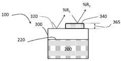
本開示の第1の態様は、低コントラストの反射防止コーティングを備えた物品に関する。図2に示されるように、物品100は、少なくとも1つの基体表面220を有する基体200と、被覆表面320を形成する、その少なくとも1つの基体表面に配置された、物品の反射率を低下させる反射防止コーティング300とを備えている。言い換えると、被覆表面320は、低反射率、またはその上に反射防止コーティング300が配置されていない基体表面220の反射率より低い反射率を示す。ここに用いたように、「反射率」という用語は、材料(例えば、物品、基体、または光学膜またはその一部)から反射した、所定の波長範囲内の入射光パワーの百分率と定義される。反射率は、特定の線幅を使用して測定される。1つ以上の実施の形態において、反射率の特性化のスペクトル分解能は、5nmまたは0.02eV未満である。 A first aspect of the present disclosure relates to an article with a low contrast antireflective coating. As shown in FIG. 2, the
ここに記載された平均反射率(%Rav1および%Rav2)および反射率(%R1および%R2)の値および範囲は、入射照明角の下で測定してよく、これは、視覚が変化するにつれて、被覆表面の反射が示すまたは知覚される色を刺激する。入射照明角は、約0度から約80度、約0度から約75度、約0度から約70度、約0度から約65度、約0度から約60度、約0度から約55度、約0度から約50度、約0度から約45度、約0度から約40度、約0度から約35度、約0度から約30度、約0度から約25度、約0度から約20度、約0度から約15度、約5度から約80度、約5度から約80度、約5度から約70度、約5度から約65度、約5度から約60度、約5度から約55度、約5度から約50度、約5度から約45度、約5度から約40度、約5度から約35度、約5度から約30度、約5度から約25度、約5度から約20度、約5度から約15度の範囲、並びにそれらの間の全ての範囲および部分的な範囲にあってよい。ここに記載された平均反射率(%Rav1および%Rav2)および反射率(%R1および%R2)の値および範囲を測定するために使用される光源としては、A光源(タングステン照明を表す)、B光源(日光擬似光源)、C光源(日光擬似光源)、D光源群(自然照明を表す)、およびF光源群(様々なタイプの蛍光照明を表す)を含む、CIEが決定した標準光源が挙げられるであろう。The average reflectance (%Rav1 and %Rav2 ) and reflectance (%R1 and %R2 ) values and ranges described herein may be measured under an incident illumination angle, which is a visual changes, it stimulates the color exhibited or perceived by the reflection of the coated surface. The incident illumination angle is about 0 degrees to about 80 degrees, about 0 degrees to about 75 degrees, about 0 degrees to about 70 degrees, about 0 degrees to about 65 degrees, about 0 degrees to about 60 degrees, about 0 degrees to about 55 degrees, about 0 degrees to about 50 degrees, about 0 degrees to about 45 degrees, about 0 degrees to about 40 degrees, about 0 degrees to about 35 degrees, about 0 degrees to about 30 degrees, about 0 degrees to about 25 degrees , about 0 degrees to about 20 degrees, about 0 degrees to about 15 degrees, about 5 degrees to about 80 degrees, about 5 degrees to about 80 degrees, about 5 degrees to about 70 degrees, about 5 degrees to about 65 degrees, about 5 degrees to about 60 degrees, about 5 degrees to about 55 degrees, about 5 degrees to about 50 degrees, about 5 degrees to about 45 degrees, about 5 degrees to about 40 degrees, about 5 degrees to about 35 degrees, about 5 degrees from about 30 degrees, from about 5 degrees to about 25 degrees, from about 5 degrees to about 20 degrees, from about 5 degrees to about 15 degrees, and all ranges and subranges therebetween. The illuminant used to measure the average reflectance (%Rav1 and %Rav2 ) and reflectance (%R1 and %R2 ) values and ranges described herein was the A illuminant (tungsten illumination). ), B illuminant (sunlight simulating), C illuminant (sunlight simulating), D illuminant group (representing natural lighting), and F illuminant group (representing various types of fluorescent lighting), determined by the CIE standard light source.
反射防止コーティング300は、その反射防止コーティング内またはその上の表面欠陥のコントラストまたは視認性が、従来の反射防止コーティングと比べて低減しているので、「低コントラスト」コーティングと記載することができる。コントラストおよび視認性は、表面欠陥を有する表面と、有さない表面との間の相対反射率に関して記載されることがある。
したがって、清浄な状態の反射防止コーティングおよび表面欠陥を含む状態の同じコーティングの反射率の相対的差異を使用して、ここに記載される反射防止コーティングの低コントラストの属性を記載することができる。詳しくは、清浄な状態にある反射防止コーティングおよび表面欠陥を有する状態にある反射防止コーティングにおける、反射率の比(すなわち、コントラスト比)、反射率振動対波長、およびコントラスト比の振動対波長の各々は、個々と、集団で、反射防止コーティングおよびその中に含まれる表面欠陥の視認性および色に影響する。それゆえ、反射率およびコントラスト比におけるより低いまたはより小さい振動、およびより小さいコントラスト比は、表面欠陥のより低い視認性に寄与する。そのような表面欠陥は、しばしば、欠陥のサイズと形状のために光散乱を生じ得る;1つ以上の実施の形態の反射防止コーティングの性能は、一般に、散乱効果を無視する。散乱効果は、ここに記載された他の光学的挙動には関係ない。表面欠陥からの光散乱の存在下でさえ、ここに記載された反射防止コーティングの実施の形態の光学的性能は、表面欠陥の視認性を著しく低下させる。 Therefore, the relative difference in reflectance of an antireflective coating in a clean state and the same coating in a state containing surface defects can be used to describe the low contrast attribute of the antireflective coatings described herein. Specifically, the reflectance ratio (i.e., contrast ratio), the reflectance oscillation versus wavelength, and the contrast ratio oscillation versus wavelength for the antireflective coating in its clean state and in its state with surface defects, respectively. individually and collectively affect the visibility and color of antireflective coatings and surface defects contained therein. Therefore, lower or smaller oscillations in reflectance and contrast ratios, and smaller contrast ratios contribute to lower visibility of surface defects. Such surface defects can often cause light scattering due to the size and shape of the defect; the performance of antireflective coatings of one or more embodiments generally ignores scattering effects. Scattering effects are not related to the other optical behaviors described here. Even in the presence of light scattering from surface defects, the optical performance of the antireflective coating embodiments described herein significantly reduces the visibility of surface defects.
1つ以上の実施の形態において、被覆表面320は、その被覆表面が清浄な状態にあるときの、可視スペクトルの少なくとも一部に亘る第1の平均反射率(%Rav1)または第1の反射率(%R1)、および被覆表面がここに記載されたような表面欠陥340を含むときの、可視スペクトルの少なくとも一部に亘る第2の平均反射率(%Rav2)または第2の反射率(%R2)を示す。%R1と%R2との間、並びに%Rav1と%Rav2との間の相対的差異は、公知のコーティングと比べて低下している。ここに用いたように、「可視スペクトル」という句は、約400nmから約700nm、または約450nmから約650nmの範囲に沿った波長を含む。ここに記載された反射率値または範囲は、その可視スペクトルに亘る、またはその可視スペクトルの一部に沿うと、認定されてもよい。可視スペクトルの一部は「波長幅」と記載されることがあり、これは、可視スペクトル内の約100nmまたは200nmの幅(例えば、約400nmから約500nm、または約450nmから約650nm)であってよい。In one or more embodiments, the
1つ以上の特別な実施の形態において、表面欠陥340は、図2に示されるように、約25nm以上の、被覆表面からの反射防止コーティングの表面厚360の除去を含む。いくつかの実施の形態において、その表面厚は、約25nmから約500nmの範囲にあることがある。例えば、その表面厚は、約25nmから約450nm、約25nmから約400nm、約25nmから約350nm、約25nmから約300nm、約25nmから約250nm、約25nmから約200nm、約25nmから約150nm、約25nmから約100nm、約50nmから約500nm、約75nmから約500nm、約100nmから約500nm、約150nmから約500nm、約200nmから約500nm、約250nmから約500nm、または約300nmから約500nmの範囲にあることがある。 In one or more particular embodiments,
いくつかの実施の形態において、反射防止コーティングは、前記表面厚より大きい厚さを有する。表面厚の除去により、除去区域に表面欠陥340が形成される一方で、残りの被覆表面320は、表面欠陥が存在しないので、清浄な状態を形成するであろう。 In some embodiments, the antireflective coating has a thickness greater than the surface thickness. The removal of the surface thickness will create
図3に示されるようないくつかの実施の形態において、反射防止コーティング300は、第1の層311が基体表面220上に配置され、第2の層312が第1の層311上に配置されるように、少なくとも2つの層を備えた多層コーティングを含む。第2の層312は、表面厚360より小さい層厚314を有することがある。言い換えれば、表面厚360は、表面厚360の除去が、被覆表面320からの第2の層312の少なくとも一部の除去を含むように、第2の層312の層厚314以上である。そのような実施の形態において、被覆表面320は、第2の層から形成された区域(清浄な状態を提供するであろう)、および第1の層311から形成された区域(表面欠陥340を含む)を含む。 In some embodiments, as shown in FIG. 3, the
図4に示されるように、1つ以上の実施の形態の表面欠陥340は、反射防止コーティング300の被覆表面320への材料または汚染物質365(例えば、指紋、指紋残留物または指紋擬似媒質)の付加を含むことがある。いくつかの実施の形態において、汚染物質365は、約100nmから約2000nmの範囲の厚さを有する平面層として存在することがある。特別な実施の形態において、その厚さは、指紋の液滴を擬似する意図がある。その汚染物質は、指紋残留物に含まれる油を擬似するために、約1.4から約1.6の範囲にある、または約1.49の屈折率を有することがある。いくつかの実施の形態において、%R1および/または%Rav1、並びに%R2および/または%Rav2は、表面欠陥が表面厚の除去または汚染物質の付加を含む場合の反射率を測定するために使用されるのと同じ技法を使用して測定してよい。汚染物質の付加を含む表面欠陥を有する他の実施の形態において、%R1および/または%Rav1は、反射防止コーティングが浸された状態、もしくは空気中にあるまたは空気に囲まれているときに測定またはモデル化されるであろう(すなわち、空気/反射防止コーティングの界面での%R1および/または%Rav1は、反射率測定系により得られる)。そのような実施の形態において、%R2および/または%Rav2は、反射防止コーティングが浸された状態、もしくは汚染物質中にあるまたは汚染物質に囲まれているときに測定またはモデル化されるであろう(すなわち、空気/汚染物質の界面での%R2および/または%Rav2は、反射率測定系により得られるが、系内のどの空気界面からの反射率も、除去されるまたは減じられる)。検出器または測定系レンズは、これも物品の被覆表面を取り囲んでいる汚染物質浴と接触していることがある。As shown in FIG. 4,
1つ以上の実施の形態において、%Rav2は、%Rav1以下であることがある。1つ以上の実施の形態において、%Rav1は、全可視スペクトルまたは可視スペクトルの少なくとも一部に亘り、約0.5%から約7%、または約0.6%から約6.0%の範囲にあることがある。1つ以上の実施の形態において、%Rav2は、全可視スペクトルまたは可視スペクトルの少なくとも一部に亘り、約10%以下(例えば、約8%以下、約6%以下、約5%以下、約4%以下、約3%以下、または約2%以下)である、または約0.1%から約8%の範囲にあることがある。表面欠陥が汚染物質の付加を含む場合、%Rav2は、可視スペクトルの少なくとも一部に亘り、約2%以下、1%以下、または約0.5%以下であることがある。In one or more embodiments, %Rav2 may be less than or equal to %Rav1 . In one or more embodiments, %Rav1 is from about 0.5% to about 7%, or from about 0.6% to about 6.0%, over the entire visible spectrum or at least a portion of the visible spectrum. may be in range. In one or more embodiments, % Rav2 is about 10% or less (eg, about 8% or less, about 6% or less, about 5% or less, about 4% or less, about 3% or less, or about 2% or less), or in the range of about 0.1% to about 8%. If the surface defects include the addition of contaminants, %Rav2 may be less than or equal to about 2%, less than or equal to 1%, or less than or equal to about 0.5% over at least a portion of the visible spectrum.
%R1および%R2の少なくとも一方は、反射率が測定される可視スペクトルに亘り、振動を示すことがある。%R1および%R2の少なくとも一方は、可視スペクトルに亘り、約2%以下の絶対反射率の平均振動振幅を含むことがある。ここに用いたように、「振幅」という用語は、可視スペクトルまたは所定の波長幅に亘る、反射率(または透過率)の山から谷の変化を含む。「平均振動振幅」という句は、可視スペクトル内の全ての可能な100nm波長範囲または所定の波長幅に亘り平均化された反射率または透過率の山から谷の変化を含む。いくつかの実施の形態において、平均振動振幅は、全可視スペクトルまたは約100nmの所定の波長幅に亘り、絶対反射率で、約1.75%以下、約1.5%以下、約1%以下、約0.75%以下、約0.5%以下、約0.25%以下、または約0.1%以下であることがある。ある場合には、平均振動振幅の下限は、約0.1%であることがある。したがって、%R1および%R2の少なくとも一方の平均振動振幅は、全可視スペクトルまたは約100nmの所定の波長幅に亘り、絶対反射率で、約0.1%から約2%の範囲にあるであろう。振動の程度は、可視スペクトルまたは所定の波長幅に亘り、平均反射率または透過率の値に対するパーセントで記載されることもある。例えば、%R1および%R2の少なくとも一方は、可視スペクトルまたは所定の波長幅に亘り、平均反射率値に対して、約30%未満、約20%未満、または約10%未満の反射率振動を示すことがある。表面欠陥が汚染物質の付加を含む、1つ以上の実施の形態において、被覆表面は、可視スペクトルに亘り、約8%以下の最大反射率値を示し、必要に応じて、可視スペクトルに亘り、約7.5%以下の絶対反射率(例えば、約6%、5%または約4%以下の絶対反射率)の最大振動振幅を含む。At least one of %R1 and %R2 may exhibit oscillations across the visible spectrum over which reflectance is measured. At least one of %R1 and %R2 may include an average vibrational amplitude of absolute reflectance of less than or equal to about 2% across the visible spectrum. As used herein, the term "amplitude" includes the peak-to-valley variation of reflectance (or transmittance) over the visible spectrum or a given wavelength band. The phrase "average vibrational amplitude" includes the peak-to-valley variation of reflectance or transmittance averaged over all possible 100 nm wavelength ranges or predetermined wavelength widths in the visible spectrum. In some embodiments, the average vibration amplitude is no more than about 1.75%, no more than about 1.5%, no more than about 1% absolute reflectance over the entire visible spectrum or a predetermined wavelength width of about 100 nm. , about 0.75% or less, about 0.5% or less, about 0.25% or less, or about 0.1% or less. In some cases, the lower bound on the average vibration amplitude may be about 0.1%. Thus, the average vibrational amplitude of at least one of %R1 and %R2 is in the range of about 0.1% to about 2% absolute reflectance over the entire visible spectrum or over a given wavelength width of about 100 nm. Will. The degree of vibration is sometimes described as a percentage of the average reflectance or transmittance value over the visible spectrum or a given wavelength band. For example, at least one of %R1 and %R2 is less than about 30%, less than about 20%, or less than about 10% reflectance over the visible spectrum or predetermined wavelength band relative to the average reflectance value. May exhibit vibration. In one or more embodiments, wherein the surface defects include the addition of contaminants, the coated surface exhibits a maximum reflectance value of less than or equal to about 8% across the visible spectrum, optionally across the visible spectrum, including a maximum vibration amplitude of about 7.5% absolute reflectance or less (eg, about 6%, 5%, or about 4% absolute reflectance or less).
1つ以上の実施の形態において、被覆表面は、%Rav2および%Rav1が同じ入射照明角で測定されるという条件で、可視スペクトルまたは所定の波長幅に亘る、第1の平均反射率に対する第2の平均反射率の比(%Rav2:%Rav1)として測定されるコントラスト比を含む。1つ以上の実施の形態において、そのコントラスト比は、約0.5から約50の範囲にあることがある。例えば、コントラスト比は、約0.5から約45、約0.5から約40、約0.5から約35、約0.5から約30、約0.5から約25、約0.5から約20、約0.5から約15、約0.5から約10、約0.5から約8、約0.5から約6、または約0.5から約5の範囲にあることがある。比較のために、約25nmから約500nmの表面厚が除去された表面欠陥を有する、公知の反射防止コーティングは、典型的に、約100以上のコントラスト比を示す。ある場合には、反射防止コーティングのコントラスト比は、表面欠陥に関連付けられることがある。例えば、表面欠陥が約25nmまでの表面厚の除去を含む場合、コントラスト比は、約10以下、約5以下、または約2以下(下限は約0.5である)であることがある;および%Rav2は、約6%以下、4%以下、または3%以下であることがある。別の例では、表面欠陥が約50nmまでの表面厚の除去を含む場合、コントラスト比は、約20以下、10以下、約5以下、約3以下、または約2以下(下限は約0.5である)であることがある;および%Rav2は、約8%以下、約6%以下、または約5%以下であることがある。さらに別の例では、表面欠陥が約100nmまでの表面厚の除去を含む場合、コントラスト比は、約50以下、20以下、10以下、約5以下、または約3以下(下限は約0.5である)であることがある;および%Rav2は、約12%以下、約8%以下、約7%以下、または約6%以下であることがある。別の例では、表面欠陥が約500nmまでの表面厚の除去を含む場合、コントラスト比は、約50以下、20以下、10以下、約5以下、または約3以下(下限は約0.5である)であることがある;および%Rav2は、約12%以下であることがある。表面欠陥が汚染物質の付加を含む実施の形態において、コントラスト比は、約20以下、約10以下、約8以下、約6以下、約5以下、約4以下、約3以下、約2以下であることがある(下限は約0.5である)。そのようなコントラスト比および/または%Rav2値は、約400nmから約700nm、または約450nmから約650nmの範囲にある可視スペクトルに沿うことがある。In one or more embodiments, thecoated surface has a first averagereflectance of Includes contrast ratio, measured as the ratio of second average reflectances (% Rav2 : % Rav1 ). In one or more embodiments, the contrast ratio may range from about 0.5 to about 50. For example, the contrast ratio is about 0.5 to about 45, about 0.5 to about 40, about 0.5 to about 35, about 0.5 to about 30, about 0.5 to about 25, about 0.5. from about 20, from about 0.5 to about 15, from about 0.5 to about 10, from about 0.5 to about 8, from about 0.5 to about 6, or from about 0.5 to about 5 be. For comparison, known antireflective coatings having surface defects removed from a surface thickness of about 25 nm to about 500 nm typically exhibit a contrast ratio of about 100 or greater. In some cases, the contrast ratio of antireflective coatings may be related to surface defects. For example, if the surface defect comprises removal of a surface thickness of up to about 25 nm, the contrast ratio may be about 10 or less, about 5 or less, or about 2 or less (with a lower limit of about 0.5); and % Rav2 may be about 6% or less, 4% or less, or 3% or less. In another example, if the surface defect includes removal of a surface thickness of up to about 50 nm, the contrast ratio is about 20 or less, 10 or less, about 5 or less, about 3 or less, or about 2 or less (with a lower limit of about 0.5 and % Rav2 can be about 8% or less, about 6% or less, or about 5% or less. In yet another example, if the surface defect comprises removal of a surface thickness of up to about 100 nm, the contrast ratio is about 50 or less, 20 or less, 10 or less, about 5 or less, or about 3 or less (with a lower limit of about 0.5 and % Rav2 can be about 12% or less, about 8% or less, about 7% or less, or about 6% or less. In another example, if the surface defect comprises removal of a surface thickness of up to about 500 nm, the contrast ratio is about 50 or less, 20 or less, 10 or less, about 5 or less, or about 3 or less, with a lower limit of about 0.5. and the % Rav2 may be about 12% or less. In embodiments where the surface defects include the addition of contaminants, the contrast ratio is about 20 or less, about 10 or less, about 8 or less, about 6 or less, about 5 or less, about 4 or less, about 3 or less, about 2 or less. (lower limit is about 0.5). Such contrast ratios and/or %Rav2 values may be along the visible spectrum ranging from about 400 nm to about 700 nm, or from about 450 nm to about 650 nm.
1つ以上の実施の形態において、被覆表面のコントラスト比は、振動を示すことがある。表面欠陥が表面厚の除去を含むいくつかの実施の形態において、コントラスト比は、可視スペクトルまたは所定の波長幅に亘り、絶対比の単位で、約2以下、約1以下、または約0.5以下の平均振動振幅を有する。表面欠陥が汚染物質の付加を含むいくつかの実施の形態において、コントラスト比は、可視スペクトルまたは所定の波長幅に亘り、絶対比の単位で、約10以下、約7以下、または約5以下の平均振動振幅を有する。 In one or more embodiments, the contrast ratio of the coated surface may exhibit oscillations. In some embodiments, the surface defects comprise removal of surface thickness, the contrast ratio is about 2 or less, about 1 or less, or about 0.5 in absolute ratio units across the visible spectrum or predetermined wavelength width. It has an average vibration amplitude of In some embodiments where the surface defects include the addition of contaminants, the contrast ratio is about 10 or less, about 7 or less, or about 5 or less, in absolute ratio units, across the visible spectrum or predetermined wavelength band. has an average vibration amplitude.
1つ以上の実施の形態の反射防止コーティング300の性能は、物品の反射率または透過率における色変化で記載されることがある。色は、国際照明委員会(「CIE」)のL*、a*、b*測色系の下での色値または座標(a*、b*)により示されることがある。色変化は、被覆表面のa*およびb*座標を使用した、以下の式√((a*2-a*1)2+(b*2-b*1)2)により決定される色ずれとして記載されることがある。座標a*1およびb*1は、1)清浄な状態または被覆表面が清浄な状態にある区域での色座標;2)(0、0);または3)基準色座標であってよい。座標a*2およびb*2は、表面欠陥の形成後の、または表面欠陥を含む区域での、被覆表面の色座標であってよい。色座標(a*1、b*1)および(a*2、b*2)を測定する場合、入射照明角および光源は同じである。いくつかの実施の形態において、色ずれは、Δa*b*と記載されることがあり、ここに記載された入射照明角(たとえば、約0度から約75度、約0度から約30度、または約30度から約75度)およびここに記載された光源下で、約6以下であることがある。いくつかの実施の形態において、色ずれは、約5.5以下、約5以下、約4.5以下、約4以下、約3.5以下、約3以下、約2.5以下、約2以下、約1.9以下、1.8以下、1.7以下、1.6以下、1.5以下、1.4以下、1.3以下、1.2以下、1.1以下、1以下、0.9以下、0.8以下、0.7以下、0.6以下、0.5以下、0.4以下、0.3以下、0.2以下、または0.1以下であることがある。いくつかの実施の形態において、色ずれは、約0であることがある。いくつかの実施の形態において、被覆表面は、表面欠陥が、約0.1nmから約200nm、または約0.1nmから約150nm、または約0.1nmから約140nmの範囲の表面厚の除去を含む場合、そのような色ずれ範囲を示す。1つ以上の特別な実施の形態において、入射照明角が約60度であり、表面厚が約0.1から約100nmの範囲にある場合、色ずれは約3以下である。The performance of one or more embodiments of
1つ以上の実施の形態において、反射防止コーティングは、複数の層を備えることがある。ある場合には、反射防止コーティングは、基体表面220上に配置された第1の層311、および第1の層上に配置された第2の層312を備えることがあり、この第1の層311は高屈折率材料(例えば、第2の層312の屈折率より大きい屈折率を有する)から作られている。ある場合には、第1の層311の厚さは、約50nm以下であることがある。いくつかの実施の形態において、高屈折率材料を含む反射防止コーティングの層の複数またさらには全てが、約100nm以下、または約50nm以下の厚さを有することがある。 In one or more embodiments, the antireflective coating may comprise multiple layers. In some cases, the antireflective coating may comprise a
反射防止コーティング300および/または物品100は、バーコビッチ圧子硬度試験により測定した硬度で記載されることがある。ここに用いたように、「バーコビッチ圧子硬度試験」は、ある材料の硬度をその表面上で、ダイヤモンド製バーコビッチ圧子をその表面に押し込むことにより、測定する工程を有する。バーコビッチ圧子硬度試験は、一般に、Oliver, W.C.; Pharr, G. M. An improved technique for determining hardness and elastic modulus using load and displacement sensing indentation experiments. J. Mater. Res., Vol. 7, No. 6, 1992, 1564-1583;およびOliver, W.C.; Pharr, G.M. Measurement of Hardness and Elastic Modulus by Instrument Indentation: Advances in Understanding and Refinements to Methodology. J. Mater. Res., Vol. 19, No. 1, 2004, 3-20に述べられた方法を使用して、物品の被覆表面320または反射防止コーティングの表面(もしくはここに記載したような、反射防止コーティングの層のいずれか1つ以上の表面)にダイヤモンド製バーコビッチ圧子を押し込んで、約50nmから約1000nmの範囲にある押込み深さまで圧痕を形成する工程、および全押込み深さ範囲またはこの押し込み深さの一部(例えば、約100nmから約600nmの範囲)に沿ってこの圧痕から最大硬度を測定する工程を有する。ここに用いたように、硬度は、最大硬度を指し、平均硬度ではない。
いくつかの実施の形態において、反射防止コーティング300は、バーコビッチ圧子硬度試験により、被覆表面320上で測定して、約5GPa超の硬度を示すことがある。この反射防止コーティングは、約8GPa以上、約10GPa以上、または約12GPa以上の硬度を示すことがある。ここに記載したような、反射防止コーティング300および任意の追加のコーティングを含む物品100は、バーコビッチ圧子硬度試験により、被覆表面320上で測定して、約5GPa以上、約8GPa以上、約10GPa以上、または約12GPa以上の硬度を示すことがある。そのような測定した硬度値は、約50nm以上または約100nm以上(例えば、約100nmから約300nm、約100nmから約400nm、約100nmから約500nm、約100nmから約600nm、約200nmから約300nm、約200nmから約400nm、約200nmから約500nm、または約200nmから約600nm)の押込み深さに沿って、反射防止コーティング300および/または物品100が示すことがある。 In some embodiments, the
反射防止コーティング300は、少なくとも1つの層であって、バーコビッチ圧子硬度試験により測定して、約5GPa以上、8GPa以上、10GPa以上、12GPa以上、約13GPa以上、約14GPa以上、約15GPa以上、約16GPa以上、約17GPa以上、約18GPa以上、約19GPa以上、約20GPa以上、約22GPa以上、約23GPa以上、約24GPa以上、約25GPa以上、約26GPa以上、または約27GPa以上(約50GPaまで)のそのような層の表面で測定した硬度を有する層を有することがある。そのような層の硬度は、バーコビッチ圧子硬度試験により測定して、約18GPaから約21GPaの範囲にあることがある。いくつかの実施の形態において、反射防止コーティングは、ここに定義したように、バーコビッチ圧子硬度試験により測定して、約5GPa超(例えば、約10GPa以上、約15GPa以上、または約20GPa以上)の平均硬度を有する硬質材料を含む。この硬質材料は、反射防止コーティングの層の全てに、または反射防止コーティングの1つ以上の特定の層に存在してもよい。ある場合には、反射防止コーティングは、硬質材料を含む、厚さが約1μm以上、または約2μm以上の層を備えることがある。そのような測定した硬度値は、約50nm以上または100nm以上(例えば、約100nmから約300nm、約100nmから約400nm、約100nmから約500nm、約100nmから約600nm、約200nmから約300nm、約200nmから約400nm、約200nmから約500nm、または約200nmから約600nm)の押込み深さに沿って、その少なくとも1つの層により示されることがある。1つ以上の実施の形態において、物品は、基体の硬度(被覆表面と反対の表面で測定できる)より大きい硬度を示す。 The
1つ以上の実施の形態において、反射防止コーティング300または反射防止コーティング内の個別の層は、表面をバーコビッチ圧子で押し込むことにより、被覆表面320上で測定して、約75GPa以上、約80GPa以上、または約85GPa以上の弾性率を示すことがある。これらの弾性率値は、例えば、0~50nmの押込み深さで、被覆表面320に非常に近く測定した弾性率を示してもよい、または例えば、約50~1000nmの、より深い押込み深さで測定した弾性率を示してもよい。 In one or more embodiments, the
前記反射防止コーティングは、その内容がここに引用される、「Scratch-Resistant Articles with a Gradient Layer」と題する、2014年4月25日に出願された、米国特許出願第14/262224号明細書に記載されているように、その厚さの少なくとも一部に沿って、屈折率勾配を有することがある。詳しくは、反射防止コーティングは、第1の表面(基体表面220に隣接した)から第2の表面(すなわち、被覆表面)まで増加する屈折率を有することがある。その屈折率は、約0.2/μmから約0.5/μmの範囲の平均比率で、その屈折率勾配に沿って増加することがあり、約1.5から約2.0の範囲にあることがある。その反射防止コーティングは、Si、Al、N、およびOの内の少なくとも2つを含む組成勾配を有することがある。 The antireflective coating is described in U.S. patent application Ser. As noted, it may have a refractive index gradient along at least a portion of its thickness. Specifically, an antireflective coating may have an index of refraction that increases from a first surface (adjacent substrate surface 220) to a second surface (ie, the coated surface). The refractive index may increase along the refractive index gradient at an average rate ranging from about 0.2/μm to about 0.5/μm, and ranging from about 1.5 to about 2.0. There is something. The antireflective coating may have a compositional gradient including at least two of Si, Al, N, and O.
他の実施の形態において、反射防止コーティングは、その内容がここに引用される、「Low-Color Scratch-Resistant Articles with a Multilayer Optical Film」と題する、2014年4月25日に出願された、米国特許出願第14/262066号明細書に記載されているように、異なる、必要に応じて交互の屈折率を有する、1つ以上の層を備えることがある。詳しくは、その反射防止コーティングは、第1の低屈折率(RI)副層および第2の高RI副層を備えることがある。随意的な第3の副層も備わってもよい。1つ以上の実施の形態において、反射防止コーティングは、複数の副層の組を備えることがある。1つの副層の組は、第1の低RI副層、第2の高RI副層および必要に応じて、第3の副層を備えることがある。いくつかの実施の形態において、反射防止コーティングは、第1の低RI副層(説明のために「L」と称する)および第2の高RI副層(説明のために「H」と称する)が、第1の低RI副層および第2の高RI副層が光学干渉層の物理的厚さに沿って交互に現れるように、副層の以下の順序:L/H/L/HまたはH/L/H/Lを提供するように、複数の副層の組を含むことがある。ある場合には、反射防止コーティングは、3組の副層の組または10組までの副層の組を有することがある。例えば、反射防止コーティングは、約2から約12組の副層の組、約3から約8組の副層の組、約3から約6組の副層の組を備えることがある。いくつかの例に使用される第3の副層は、低RI、高RI、または中間RIを有してもよい。いくつかの実施の形態において、第3の副層は、第1の低RI副層または第2の高RI副層と同じRIを有してもよい。他の実施の形態において、第3の副層は、第1の低RI副層のRIと第2の高RI副層のRIとの間の中間RIを有してもよい。第3の副層は、複数組の副層の組と機能性コーティング(ここに記載されるような)(図示せず)との間、または基体と、複数組の副層の組(図示せず)との間に配置されてもよい。あるいは、第3の副層は、複数組の副層の組(図示せず)内に含まれてもよい。第3の副層は、以下の例示の構成で反射防止コーティング中に設けられてもよい:L第3の副層/H/L/H/L;H第3の副層/L/H/L/H;L/H/L/H/L第3の副層;H/L/H/L/H第3の副層;L第3の副層/H/L/H/L/H第3の副層;H第3の副層/L/H/L/H/L第3の副層;L第3の副層/L/H/L/H;H第3の副層/H/L/H/L;H/L/H/L/L第3の副層;L/H/L/H/H第3の副層;L第3の副層/L/H/L/H/H第3の副層;H第3の副層/H/L/H/L/L第3の副層;L/M/H/L/M/H;H/M/L/H/M/L;M/L/H/L/M;および他の組合せ。これらの構成において、下付文字のない「L」は、第1の低RI副層を称し、下付文字のない「H」は第2の高RI副層を称する。「L第3の副層」への言及は、低RIを有する第3の副層を称し、「H第3の副層」は、高RIを有する第3の副層を称し、「M」は、中間RIを有する第3の副層を称する。In another embodiment, the anti-reflection coating is a U.S. As described in patent application Ser. No. 14/262066, it may comprise one or more layers having different, optionally alternating, indices of refraction. Specifically, the antireflective coating may comprise a first low refractive index (RI) sublayer and a second high RI sublayer. An optional third sublayer may also be provided. In one or more embodiments, an antireflective coating may comprise multiple sets of sublayers. One sublayer set may comprise a first low RI sublayer, a second high RI sublayer and optionally a third sublayer. In some embodiments, the antireflective coating comprises a first low RI sublayer (referred to as "L" for discussion) and a second high RI sublayer (referred to as "H" for discussion). but the following order of sublayers: L/H/L/H or Multiple sets of sublayers may be included to provide H/L/H/L. In some cases, the antireflective coating may have 3 sublayer sets or up to 10 sublayer sets. For example, the antireflective coating may comprise from about 2 to about 12 sublayer sets, from about 3 to about 8 sublayer sets, from about 3 to about 6 sublayer sets. A third sublayer used in some examples may have a low RI, a high RI, or a medium RI. In some embodiments, the third sublayer may have the same RI as the first low RI sublayer or the second high RI sublayer. In other embodiments, the third sublayer may have an intermediate RI between the RI of the first low RI sublayer and the RI of the second high RI sublayer. A third sublayer may be between the set of sublayers and the functional coating (as described herein) (not shown) or the substrate and the set of sublayers (not shown). may be placed between Alternatively, the third sublayer may be included in multiple sets of sublayer sets (not shown). A third sublayer may be provided in the antireflective coating in the following exemplary configurations: Lthird sublayer /H/L/H/L; Hthird sublayer /L/H/ L/H; L/H/L/H/L3rd sublayer ; H/L/H/L/H3rd sublayer ; L3rd sublayer /H/L/H/L/HThird sublayer ; Hthird sublayer /L/H/L/H/Lthird sublayer ; Lthird sublayer /L/H/L/H; Hthird sublayer / H/L/H/L; H/L/H/L/Lthird sublayer ; L/H/L/H/Hthird sublayer ; Lthird sublayer /L/H/L /H/Hthird sublayer ; Hthird sublayer /H/L/H/L/Lthird sublayer ; L/M/H/L/M/H; H/M/L/ H/M/L; M/L/H/L/M; and other combinations. In these configurations, the "L" without subscript refers to the first low RI sublayer and the "H" without subscript refers to the second high RI sublayer. References to "L3rd sublayer " refer to the 3rd sublayer with low RI, "H3rd sublayer " refers to the 3rd sublayer with high RI, and "M" refers to the third sublayer with intermediate RI.
ここに用いたように、「低RI」、「高RI」、および「中間RI」という用語は、そのRIの別のRIに対する相対値を指す(例えば、低RI<中間RI<高RI)。1つ以上の実施の形態において、第1の低RI副層または第3の副層について使用した場合、「低RI」という用語は、約1.3から約1.7の範囲を含む。1つ以上の実施の形態において、第2の高RI副層または第3の副層について使用した場合、「高RI」という用語は、約1.6から約2.5の範囲を含む。いくつかの実施の形態において、「中間RI」という用語は、第3の副層について使用した場合、約1.55から約1.8の範囲を含む。ある場合には、低RI、高RIおよび中間RIの範囲は、重複することもある;しかしながら、ほとんどの場合、光学干渉層の副層は、低RI<中間RI<高RIのRIに関する一般的な関係を有する。 As used herein, the terms "low RI", "high RI", and "intermediate RI" refer to the relative value of that RI to another RI (eg, low RI<intermediate RI<high RI). In one or more embodiments, the term "low RI" when used with respect to the first low RI sublayer or the third sublayer includes a range of about 1.3 to about 1.7. In one or more embodiments, the term "high RI" when used with respect to the second high RI sublayer or the third sublayer includes a range of about 1.6 to about 2.5. In some embodiments, the term "intermediate RI" when used for the third sublayer includes a range of about 1.55 to about 1.8. In some cases, the ranges of low RI, high RI and medium RI may overlap; have a relationship
反射防止コーティングに使用するのに適した例示の材料としては、SiO2、Al2O3、GeO2、SiO、AlOxNy、AlN、Si3N4、SiOxNy、SiuAlvOxNy、Ta2O5、Nb2O5、TiO2、ZrO2、TiN、MgO、MgF2、BaF2、CaF2、SnO2、HfO2、Y2O3、MoO3、DyF3、YbF3、YF3、CeF3、高分子、フルオロポリマー、プラズマ重合高分子、シロキサンポリマー、シルセスキオキサン、ポリイミド、フッ素化ポリイミド、ポリエーテルイミド、ポリエーテルスルホン、ポリフェニルスルホン、ポリカーボネート、ポリエチレンテレフタレート、ポリエチレンナフタレート、アクリルポリマー、ウレタンポリマー、ポリメチルメタクリレート、耐引掻性層に使用するのに適していると下記に挙げられる他の材料、および当該技術分野に公知の他の材料が挙げられる。第1の低RI副層に使用するのに適した材料のいくつかの例としては、SiO2、Al2O3、GeO2、SiO、AlOxNy、SiOxNy、SiuAlvOxNy、MgO、MgF2、BaF2、CaF2、DyF3、YbF3、YF3、およびCeF3が挙げられる。第2の高RI副層に使用するのに適した材料のいくつかの例としては、SiuAlvOxNy、Ta2O5、Nb2O5、AlN、Si3N4、AlOxNy、SiOxNy、HfO2、TiO2、ZrO2、Y2O3、Al2O3、およびMoO3が挙げられる。Exemplary materials suitable for use in antireflectivecoatings includeSiO2 ,Al2O3 ,GeO2 ,SiO ,AlOxNy ,AlN ,Si3N4,SiOxNy ,SiuAlv.OxNy ,Ta2O5 ,Nb2O5,TiO2 ,ZrO2 ,TiN , MgO,MgF2 ,BaF2 ,CaF2 ,SnO2 ,HfO2 ,Y2O3,MoO3,DyF3 , YbF3 , YF3 , CeF3 , polymer, fluoropolymer, plasma-polymerized polymer, siloxane polymer, silsesquioxane, polyimide, fluorinated polyimide, polyetherimide, polyethersulfone, polyphenylsulfone, polycarbonate, polyethylene Terephthalate, polyethylene naphthalate, acrylic polymers, urethane polymers, polymethyl methacrylate, other materials listed below as suitable for use in the scratch resistant layer, and other materials known in the art. be done. Some examples of materials suitable for use in the first lowRIsublayer includeSiO2 ,Al2O3,GeO2 ,SiO ,AlOxNy ,SiOxNy ,SiuAlvOxNy , MgO,MgF2 , BaF2,CaF2 ,DyF3,YbF3,YF3 , andCeF3 . Some examples of suitable materials for use in thesecondhigh RIsublayer includeSiuAlvOxNy ,Ta2O5 ,Nb2O5 ,AlN ,Si3N4,AlOxNy ,SiOxNy ,HfO2 ,TiO2,ZrO2,Y2O3,Al2O3, andMoO3 .
1つ以上の実施の形態において、副層の少なくとも1つは、特定の光学的厚さ範囲を有することがある。ここに用いたように、「光学的厚さ」という用語は、(n*d)により決定され、式中、「n」は副層のRIを称し、「d」は副層の物理的厚さを称する。1つ以上の実施の形態において、反射防止コーティングの副層の少なくとも1つは、約2nmから約200nm、約10nmから約100nm、または約15nmから約100nmの範囲の光学的厚さを有することがある。いくつかの実施の形態において、反射防止コーティング中の副層の全ては、各々、約2nmから約200nm、約10nmから約100nm、または約15nmから約100nmの範囲の光学的厚さを有することがある。ある場合には、反射防止コーティングの少なくとも1つの副層は、約50nm以上の光学的厚さを有する。ある場合には、第1の低RI副層の各々は、約2nmから約200nm、約10nmから約100nm、または約15nmから約100nmの範囲の光学的厚さを有する。他の場合には、第2の高RI副層の各々は、約2nmから約200nm、約10nmから約100nm、または約15nmから約100nmの範囲の光学的厚さを有する。さらに他の場合には、第3の副層の各々は、約2nmから約200nm、約10nmから約100nm、または約15nmから約100nmの範囲の光学的厚さを有する。In one or more embodiments, at least one of the sublayers may have a particular optical thickness range. As used herein, the term "optical thickness" is determined by (n* d), where "n" refers to the RI of the sublayer and "d" is the physical thickness of the sublayer. called. In one or more embodiments, at least one of the antireflective coating sublayers can have an optical thickness ranging from about 2 nm to about 200 nm, from about 10 nm to about 100 nm, or from about 15 nm to about 100 nm. be. In some embodiments, all of the sublayers in the antireflective coating can each have an optical thickness ranging from about 2 nm to about 200 nm, from about 10 nm to about 100 nm, or from about 15 nm to about 100 nm. be. In some cases, at least one sublayer of the antireflective coating has an optical thickness of about 50 nm or greater. In some cases, each of the first low RI sublayers has an optical thickness ranging from about 2 nm to about 200 nm, from about 10 nm to about 100 nm, or from about 15 nm to about 100 nm. In other cases, each of the second high RI sublayers has an optical thickness ranging from about 2 nm to about 200 nm, from about 10 nm to about 100 nm, or from about 15 nm to about 100 nm. In still other cases, each of the third sublayers has an optical thickness ranging from about 2 nm to about 200 nm, from about 10 nm to about 100 nm, or from about 15 nm to about 100 nm.
1つ以上の実施の形態において、反射防止コーティングの物理的厚さは約800nm以下である。反射防止コーティングの物理的厚さは、約10mmから約800nm、約50mmから約800nm、約100mmから約800nm、約150mmから約800nm、約200mmから約800nm、約10mmから約750nm、約10mmから約700nm、約10mmから約650nm、約10mmから約600nm、約10mmから約550nm、約10mmから約500nm、約10mmから約450nm、約10mmから約400nm、約10mmから約350nm、約10mmから約300nm、約50mmから約300nm、並びにそれらの間の全ての範囲および部分的な範囲にあることがある。 In one or more embodiments, the physical thickness of the antireflective coating is about 800 nm or less. The physical thickness of the antireflective coating is from about 10 mm to about 800 nm, from about 50 mm to about 800 nm, from about 100 mm to about 800 nm, from about 150 mm to about 800 nm, from about 200 mm to about 800 nm, from about 10 mm to about 750 nm, from about 10 mm to about 700 nm, about 10 mm to about 650 nm, about 10 mm to about 600 nm, about 10 mm to about 550 nm, about 10 mm to about 500 nm, about 10 mm to about 450 nm, about 10 mm to about 400 nm, about 10 mm to about 350 nm, about 10 mm to about 300 nm, It may range from about 50 mm to about 300 nm and all ranges and subranges therebetween.
基体200は、非晶質基体、結晶質基体、またはその組合せを含むことがある。基体200は、人造材料および/または自然発生物質から形成されてもよい。いくつかの特別な実施の形態において、基体200は、特に、プラスチックおよび/または金属基体を除くことがある。1つ以上の実施の形態において、基体は、約1.45から約1.55の範囲の屈折率を示す。特別な実施の形態において、基体200は、少なくとも5、少なくとも10、少なくとも15、または少なくとも20のサンプルを使用したボール・オン・リング試験を使用して測定して、0.5%以上、0.6%以上、0.7%以上、0.8%以上、0.9%以上、1%以上、1.1%以上、1.2%以上、1.3%以上、1.4%以上、1.5%以上、または2%以上の平均破壊歪みを、1つ以上の互いに反対にある主面の表面に示すことがある。特別な実施の形態において、基体200は、約1.2%、約1.4%、約1.6%、約1.8%、約2.2%、約2.4%、約2.6%、約2.8%、または約3%以上の平均破壊歪みを、1つ以上の互いに反対の主面の表面に示すことがある。適切な基体200は、約30GPaから約120GPaの範囲の弾性率(またはヤング率)を示すことがある。
1つ以上の実施の形態において、非晶質基体はガラスを含むことがあり、このガラスは、強化されていても、されていなくてもよい。適切なガラスの例としては、ソーダ石灰ガラス、アルカリアミノケイ酸塩ガラス、アルカリ含有ホウケイ酸ガラス、およびアルカリアルミノホウケイ酸塩ガラスが挙げられる。いくつかの変形において、ガラスはリチアを含まないことがある。1つ以上の代わりの実施の形態において、基体200は、ガラスセラミック基体(強化されていても、いなくてもよい)などの結晶質基体を含むことがある、またはサファイアなどの単結晶構造を含むことがある。1つ以上の特別な実施の形態において、基体200は、非晶質基材(例えば、ガラス)よび結晶質クラッド(例えば、サファイア層、多結晶アルミナ層および/またはスピネル(MgAl2O4)層)を含む。In one or more embodiments, the amorphous substrate may comprise glass, which may or may not be tempered. Examples of suitable glasses include soda lime glasses, alkali aminosilicate glasses, alkali containing borosilicate glasses, and alkali aluminoborosilicate glasses. In some variations, the glass may be free of lithia. In one or more alternative embodiments,
基体200は、実質的に平面またはシート状であってよいが、他の実施の形態は、湾曲または他に成形または造形された基体を利用してもよい。基体200は、実質的に光学的に透明(optically clear)であり、透き通り(transparent)、光散乱がないことがある。そのような実施の形態において、その基体は、約85%以上、約86%以上、約87%以上、約88%以上、約89%以上、約90%以上、約91%以上、または約92%以上の、可視光領域に亘る平均透過率を示すことがある。
それに加え、またはそれに代えて、基体200の物理的厚さは、審美的および/または機能性の理由のために、その寸法の1つ以上に沿って変動してもよい。例えば、基体200の縁は、基体200のより中央の領域と比べてより厚くてもよい。基体200の長さ、幅および物理的厚さの寸法も、物品100の用途または使用にしたがって、変動してもよい。 Additionally or alternatively, the physical thickness of
基体200は、多種多様な異なるプロセスを使用して提供してもよい。例えば、基体200がガラスなどの非晶質基体を含む場合、様々な成形方法として、フロートガラス法、並びにフュージョンドロー法およびスロットドロー法などのダウンドロー法が挙げられる。
基体200は、一旦形成されたら、強化して、強化基体を形成してもよい。ここに用いたように、「強化基体」という用語は、例えば、基体の表面内のより小さいイオンをより大きいイオンとイオン交換することにより、化学強化された基体を称することがある。しかしながら、熱的焼き戻し、または圧縮応力領域および中央引張領域を形成するために基体の部分の間の熱膨張係数の不一致を利用することなどの、当該技術分野に公知の他の強化方法を利用して、強化基体を形成してもよい。
基体がイオン交換法により化学強化される場合、基体の表面層内のイオンが、同じ価数または酸化状態を有するより大きいイオンと置換-交換-される。イオン交換法は、典型的に、基体を、その基体中のより小さいイオンと交換すべきより大きいイオンを含有する溶融塩浴中に浸漬することにより行われる。以下に限られないが、浴の組成と温度、浸漬時間、(複数の)塩浴中の基体の浸漬回数、多数の塩浴の使用、アニールや洗浄などの追加の工程を含むイオン交換法のパラメータは、概して、基体の組成、所望の圧縮応力(CS)、強化操作から生じる基体の圧縮応力層の深さ(または層の深さ)により決まることが当業者により認識されよう。一例として、アルカリ金属含有ガラス基体のイオン交換は、以下に限られないが、より大きいアルカリ金属イオンの硝酸塩、硫酸塩、および塩化物などの塩を含有する、少なくとも1つの溶融塩浴への浸漬により行われることがある。溶融塩浴の温度は、典型的に、約380℃から約450℃までの範囲にあり、一方で、浸漬時間は、約15分から約40時間に及ぶ。しかしながら、上述したものとは異なる温度および浸漬時間を使用してもよい。 When the substrate is chemically strengthened by ion exchange methods, ions in the surface layer of the substrate are displaced-exchanged-with larger ions having the same valence or oxidation state. Ion exchange methods are typically carried out by immersing the substrate in a molten salt bath containing larger ions to exchange for smaller ions in the substrate. Ion exchange methods including, but not limited to, bath composition and temperature, immersion time, number of times the substrate is immersed in the salt bath(s), use of multiple salt baths, additional steps such as annealing and washing. Those skilled in the art will appreciate that the parameters are generally determined by the composition of the substrate, the desired compressive stress (CS), and the compressive stress layer depth (or layer depth) of the substrate resulting from the strengthening operation. By way of example, ion exchange of an alkali metal-containing glass substrate includes, but is not limited to, immersion in at least one molten salt bath containing salts such as nitrates, sulfates, and chlorides of larger alkali metal ions. may be performed by The temperature of the molten salt bath typically ranges from about 380° C. to about 450° C., while immersion times range from about 15 minutes to about 40 hours. However, temperatures and immersion times different from those mentioned above may be used.
その上、ガラス基体が多数のイオン交換浴中に浸漬され、浸漬の間に洗浄および/またはアニール工程が行われる、イオン交換法の非限定的例が、ガラス基体が、多数の連続したイオン交換処理において、異なる濃度の塩浴中の浸漬により強化される、2008年7月11日に出願された米国仮特許出願第61/079995号からの優先権を主張する、「Glass with Compressive Surface for Consumer Applications」と題する、Douglas C. Allen等により2009年7月10日に出願された米国特許出願第12/500650号明細書;およびガラス基体が、流出イオンで希釈された第1の浴中のイオン交換と、その後、第1の浴より小さい濃度の流出イオンを有する第2の浴中の浸漬により強化される、2008年7月29日に出願された米国仮特許出願第61/084398号からの優先権を主張する、「Dual Stage Ion Exchange for Chemical Strengthening of Glass」と題する、2012年11月20日に発行された、Christopher M. Lee等の米国特許第8312739号明細書に記載されている。米国特許出願第12/500650号明細書および米国特許第8312739号明細書をここに全て引用する。 Moreover, a non-limiting example of an ion exchange method in which a glass substrate is immersed in multiple ion exchange baths with washing and/or annealing steps between immersion is where the glass substrate is immersed in multiple successive ion exchange baths. The treatment claims priority from U.S. Provisional Patent Application No. 61/079995, filed Jul. 11, 2008, "Glass with Compressive Surface for Consumer," enhanced by immersion in salt baths of different concentrations. No. 12/500,650, filed Jul. 10, 2009 by Douglas C. Allen et al. from U.S. Provisional Patent Application No. 61/084398, filed July 29, 2008, enhanced by exchange and subsequent immersion in a second bath having a lower concentration of effluent ions than the first bath. No. 8,312,739 to Christopher M. Lee et al., issued Nov. 20, 2012, entitled "Dual Stage Ion Exchange for Chemical Strengthening of Glass," claiming priority. US patent application Ser. No. 12/500,650 and US Pat. No. 8,312,739 are fully incorporated herein.
イオン交換により達成される化学強化の程度は、中央張力(CT)、表面CS、および層の深さ(DOL)のパラメータに基づいて、定量化されることがある。表面CSは、様々な深さでの強化ガラス内または表面近くで測定してよい。最大CS値は、強化基体の表面での実測CS(CSs)を含むことがある。ガラス基体内の圧縮応力層に隣接した内側領域について算定されるCTは、CS、物理的厚さt、およびDOLから計算することができる。CSおよびDOLは、当該技術分野で公知の手段を使用して測定される。そのような手段としては、以下に限られないが、株式会社ルケオ(日本国、東京都)により製造されているFSM-6000などの市販の装置を使用した表面応力の測定(FSM)を含み、CSおよびDOLを測定する方法は、「Standard Specification for Chemically Strengthened Flat Glass」と題するASTM 1422C-99、および「Standard Test Method for Non-Destructive Photoelastic Measurement of Edge and Surface Stresses in Annealed, Heat-Strengthened, and Fully-Tempered Flat Glass」と題するASTM1279.19779に記載されており、これらの内容をここに全て引用する。表面応力測定は、ガラス基体の複屈折に関連する応力光係数(SOC)の正確な測定に依存する。次に、SOCは、その内容がここに全て引用される、両方とも「Standard Test Method for Measurement of Glass Stress-Optical Coefficient」と題するASTM標準C770-98(2008)に記載されているファイバおよび4点曲げ法、並びにバルクシリンダ法などの当該技術分野で公知の方法により測定される。CSおよびCTの関係は、式(1):
CT=(CS・DOL)/(t-2DOL) (1)
により与えられ、式中、tはガラス物品の物理的厚さ(μm)である。本開示の様々な部分において、CTおよびCSは、ここで、メガパスカル(MPa)で表され、物理的厚さtは、マイクロメートル(μm)またはミリメートル(mm)のいずれかで表され、DOLはマイクロメートル(μm)で表されている。The degree of chemical strengthening achieved by ion exchange may be quantified based on the parameters of central tension (CT), surface CS, and depth of layer (DOL). The surface CS may be measured within or near the surface of the tempered glass at various depths. The maximum CS value may include the measured CS at the surface of the reinforced substrate (CSs ). A calculated CT for the inner region adjacent to the compressive stress layer in the glass substrate can be calculated from CS, physical thickness t, and DOL. CS and DOL are measured using means known in the art. Such means include, but are not limited to, measurement of surface stress (FSM) using commercially available equipment such as the FSM-6000 manufactured by Luceo Co., Ltd., Tokyo, Japan; Methods for measuring CS and DOL are in accordance with ASTM 1422C-99 entitled "Standard Specification for Chemically Strengthened Flat Glass" and "Standard Test Method for Non-Destructive Photoelastic Measurement of Edge and Surface Stresses in Annealed, Heat-Strengthened, and Fully ASTM 1279.19779 entitled "-Tempered Flat Glass", the contents of which are incorporated herein in their entirety. Surface stress measurements rely on accurate measurement of the stress optical coefficient (SOC), which is related to the birefringence of the glass substrate. The SOC was then tested for fiber and four-point testing as described in ASTM Standard C770-98 (2008), both entitled "Standard Test Method for Measurement of Glass Stress-Optical Coefficient", the contents of which are incorporated herein in full. It is measured by methods known in the art such as bending method and bulk cylinder method. The relationship between CS and CT is given by equation (1):
CT=(CS・DOL)/(t−2DOL) (1)
where t is the physical thickness (μm) of the glass article. In various parts of this disclosure, CT and CS are herein expressed in megapascals (MPa), physical thickness t is expressed in either micrometers (μm) or millimeters (mm), DOL is expressed in micrometers (μm).
1つの実施の形態において、強化基体200は、250MPa以上、300MPa以上、例えば、400MPa以上、450MPa以上、500MPa以上、550MPa以上、600MPa以上、650MPa以上、700MPa以上、750MPa以上、または800MPa以上の表面CSを有し得る。強化基体は、10μm以上、15μm以上、20μm以上(例えば、25μm、30μm、35μm、40μm、45μm、50μm以上)のDOLおよび/または10MPa以上、20MPa以上、30MPa以上、40MPa以上(例えば、42MPa、45MPa、または50MPa以上)であるが、100MPa未満(例えば、95、90、85、80、75、70、65、60、55MPa以下)であるCTを有することがある。1つ以上の特別な実施の形態において、強化基体は、以下の内の1つ以上を有する:500MPa超の表面CS、15μm超のDOL、および18MPa超のCT。 In one embodiment, the reinforced
基体に使用してよい例示のガラスとしては、アルカリアルミノケイ酸塩ガラス組成物またはアルカリアルミノホウケイ酸塩ガラス組成物が挙げられるが、他のガラス組成物も考えられる。そのようなガラス組成物は、イオン交換法により化学強化することができる。一例のガラス組成物は、SiO2、B2O3およびNa2Oを含み、ここで、(SiO2+B2O3)≧66モル%およびNa2O≧9モル%である。ある実施の形態において、そのガラス組成物は、少なくとも6質量%の酸化アルミニウムを含む。さらなる実施の形態において、その基体は、アルカリ土類酸化物の含有量が少なくとも5質量%であるように、1種類以上のアルカリ土類酸化物を有するガラス組成物を含む。適切なガラス組成物は、いくつかの実施の形態において、K2O、MgO、およびCaOの内の少なくとも1つをさらに含む。特別な実施の形態において、基体に使用されるガラス組成物は、61~75モル%のSiO2、7~15モル%のAl2O3、0~12モル%のB2O3、9~21モル%のNa2O、0~4モル%のK2O、0~7モル%のMgO、および0~3モル%のCaOを含んで差し支えない。Exemplary glasses that may be used for the substrate include alkali aluminosilicate glass compositions or alkali aluminoborosilicate glass compositions, although other glass compositions are also contemplated. Such glass compositions can be chemically strengthened by ion exchange methods. An example glass composition includes SiO2 , B2 O3 and Na2 O, where (SiO2 +B2 O3 )≧66 mol % and Na2 O≧9 mol %. In some embodiments, the glass composition comprises at least 6% by weight aluminum oxide. In a further embodiment, the substrate comprises a glass composition having one or more alkaline earth oxides such that the alkaline earth oxide content is at least 5% by weight. Suitable glass compositions, in some embodiments, further include atleast one of K2O, MgO, and CaO. In a particular embodiment, the glass composition used for the substrate is 61-75 mol % SiO2 , 7-15 mol % Al2 O3 , 0-12 mol % B2 O3 , 9- It may contain 21 mol % Na2 O, 0-4 mol % K2 O, 0-7 mol % MgO, and 0-3 mol % CaO.
基体に適したさらに別の例示のガラス組成物は、60~70モル%のSiO2、6~14モル%のAl2O3、0~15モル%のB2O3、0~15モル%のLi2O、0~20モル%のNa2O、0~10モル%のK2O、0~8モル%のMgO、0~10モル%のCaO、0~5モル%のZrO2、0~1モル%のSnO2、0~1モル%のCeO2、50ppm未満のAs2O3、および50ppm未満のSb2O3を含み、ここで、12モル%≦(Li2O+Na2O+K2O)≦20モル%、および0モル%≦(MgO+CaO)≦10モル%である。Yet another exemplary glass composition suitable for the substrate is 60-70 mol % SiO2 , 6-14 mol % Al2 O3 , 0-15 mol % B2 O3 , 0-15 mol %. Li2 O, 0-20 mol % Na2 O, 0-10 mol % K2 O, 0-8 mol % MgO, 0-10 mol % CaO, 0-5 mol % ZrO2 , 0-1 mol % SnO2 , 0-1 mol % CeO2 , less than 50 ppm As2 O3 , and less than 50 ppm Sb2 O3 , wherein 12 mol %≦(Li2 O+Na2 O+K2 O)≦20 mol %, and 0 mol %≦(MgO+CaO)≦10 mol %.
基体に適したさらにまた別の例示のガラス組成物は、63.5~66.5モル%のSiO2、8~12モル%のAl2O3、0~3モル%のB2O3、0~5モル%のLi2O、8~18モル%のNa2O、0~5モル%のK2O、1~7モル%のMgO、0~2.5モル%のCaO、0~3モル%のZrO2、0.05~0.25モル%のSnO2、0.05~0.5モル%のCeO2、50ppm未満のAs2O3、および50ppm未満のSb2O3を含み、ここで、14モル%≦(Li2O+Na2O+K2O)≦18モル%、および2モル%≦(MgO+CaO)≦7モル%である。Yet another exemplary glass composition suitable for the substrate is 63.5-66.5 mol % SiO2 , 8-12 mol % Al2 O3 , 0-3 mol % B2 O3 , 0-5 mol % Li2 O, 8-18 mol % Na2 O, 0-5 mol % K2 O, 1-7 mol % MgO, 0-2.5 mol % CaO, 0- 3 mol % ZrO2 , 0.05-0.25 mol % SnO2 , 0.05-0.5 mol % CeO2 , less than 50 ppm As2 O3 , and less than 50 ppm Sb2 O3 . where 14 mol %≦(Li2 O+Na2 O+K2 O)≦18 mol % and 2 mol %≦(MgO+CaO)≦7 mol %.
特別な実施の形態において、基体に適したアルカリアルミノケイ酸塩ガラス組成物は、アルミナ、少なくとも1種類のアルカリ金属およびいくつかの実施の形態において、50モル%超のSiO2、他の実施の形態において、少なくとも58モル%のSiO2、さらに他の実施の形態において、少なくとも60モル%のSiO2を含み、ここで、比(Al2O3+B2O3)/Σ改質剤>1であり、この比において、成分はモル%で表され、改質剤はアルカリ金属酸化物である。このガラス組成物は、特別な実施の形態において、58~72モル%のSiO2、9~17モル%のAl2O3、2~12モル%のB2O3、8~16モル%のNa2O、および0~4モル%のK2Oを含み、比(Al2O3+B2O3)/Σ改質剤>1である。In a particular embodiment, the alkali aluminosilicate glass composition suitable for the substrate comprises alumina, at least one alkali metal and in some embodiments greater than 50 mole %SiO2 , in other embodiments at least 58 mol%SiO2 , and in still other embodiments at least 60 mol%SiO2 , wherein the ratio(Al2O3+B2O3 )/[Sigma] modifier>1. In this ratio, the components are expressed in mol % and the modifier is the alkali metal oxide. The glass composition comprises, in a particular embodiment, 58-72 mol % SiO2 , 9-17 mol % Al2 O3 , 2-12 mol % B2 O3 , 8-16 mol % Na2 O, and 0-4 mol % K2 O with a ratio (Al2 O3 +B2 O3 )/Σ modifier>1.
さらに別の実施の形態において、基体は、64~68モル%のSiO2、12~16モル%のNa2O、8~12モル%のAl2O3、0~3モル%のB2O3、2~5モル%のK2O、4~6モル%のMgO、および0~5モル%のCaOを含むアルカリアルミノケイ酸塩ガラス組成物であって、66モル%≦SiO2+B2O3+CaO≦69モル%、Na2O+K2O+B2O3+MgO+CaO+SrO>10モル%、5モル%≦MgO+CaO+SrO≦8モル%、(Na2O+B2O3)-Al2O3≦2モル%、2モル%≦Na2O-Al2O3≦6モル%、および4モル%≦(Na2O+K2O)-Al2O3≦10モル%である、アルカリアルミノケイ酸塩ガラス組成物を含むことがある。In yet another embodiment, the substrate is 64-68 mol % SiO2 , 12-16 mol % Na2 O, 8-12 mol % Al2 O3 , 0-3 mol % B2 O.3 , an alkali aluminosilicate glass composition containing 2-5 mol% K2 O, 4-6 mol% MgO, and 0-5 mol% CaO, wherein 66 mol% ≤ SiO2 +B2 O3 + CaO ≤ 69 mol%, Na2 O + K2 O + B2 O3 + MgO + CaO + SrO > 10 mol%, 5 mol% ≤ MgO + CaO + SrO ≤ 8 mol%, (Na2 O + B2 O3 )-Al2 O3 ≤ 2 mol%, 2 comprising an alkali aluminosilicate glass composition wherein mol%≦Na2 O—Al2 O3 ≦6 mol% and 4 mol%≦(Na2 O+K2 O)—Al2 O3 ≦10 mol%. There is
代わりの実施の形態において、基体は、2モル%以上のAl2O3および/またはZrO2、または4モル%以上のAl2O3および/またはZrO2を含むアルカリアルミノケイ酸塩ガラス組成物から構成されることがある。In alternative embodiments, the substrate is from an alkali aluminosilicate glass composition comprising 2 mol % or more Al2 O3 and/or ZrO2 , or 4 mol % or more Al2 O3 and/or ZrO2 . may be configured.
基体200が結晶質基体を含む場合、その基体は単結晶を含むことがあり、その単結晶はAl2O3を含むことがある。そのような単結晶基体はサファイアと称される。結晶質基体の他の適切な材料としては、多結晶アルミナ層および/またはスピネル(MgAl2O4)が挙げられる。When
必要に応じて、結晶質基体200はガラスセラミック基体を含むことがあり、その基体は、強化されていてもされていなくてもよい。適切なガラスセラミックの例としては、Li2O-Al2O3-SiO2系(すなわち、LAS系)ガラスセラミック、MgO-Al2O3-SiO2系(すなわち、MAS系)ガラスセラミック、および/またはβ石英固溶体、βスポジュメン固溶体、コージエライト、および二ケイ酸リチウムを含む主結晶相を有するガラスセラミックが挙げられる。このガラスセラミック基体は、ここに開示された化学強化法を使用して強化してもよい。1つ以上の実施の形態において、MAS系ガラスセラミック基体は、Li2SO4溶融塩中で強化してよく、それにより、Mg2+が2つのLi+で交換され得る。If desired,
1つ以上の実施の形態による基体200は、約100μmから約5mmに及ぶ物理的厚さを有し得る。例示の基体200の物理的厚さは、約100μmから約500μm(例えば、100、200、300、400または500μm)に及ぶ。さらなる例示の基体200の物理的厚さは、約500μmから約1000μm(例えば、500、600、700、800、900または1000μm)に及ぶ。基体200は、約1mm超(例えば、約2、3、4、または5mm)の物理的厚さを有することがある。1つ以上の実施の形態において、基体200は、2mm以下、または1mm未満の物理的厚さを有することがある。基体200は、表面傷の影響をなくすまたは低下させるために、酸磨きまたは他の様式で処理されてもよい。
ここに記載された物品は、反射防止コーティングと共に他のコーティングを含んでもよい。例えば、1つ以上の耐引掻性コーティング、防指紋コーティング、抗菌コーティングおよび他のそのような機能性コーティングを物品に組み込んでもよい。他の例において、その機能性コーティングとの組合せで、複数の反射防止コーティングを使用してもよい。例えば、反射防止コーティングは、その反射防止コーティングが物品の最上層コーティングを形成するように、機能性コーティングの上面に存在してもよい。別の例において、ある反射防止コーティングが機能性コーティングの下に存在し、別の反射防止コーティングが、その機能性コーティングの上面に存在してもよい。 The articles described herein may include other coatings along with antireflective coatings. For example, one or more of scratch resistant coatings, anti-fingerprint coatings, antimicrobial coatings and other such functional coatings may be incorporated into the article. In other examples, multiple anti-reflective coatings may be used in combination with the functional coating. For example, an antireflective coating may be present on top of the functional coating such that the antireflective coating forms the topmost coating of the article. In another example, one antireflective coating may be below the functional coating and another antireflective coating may be on top of the functional coating.
反射防止コーティングおよび/または他のコーティングは、真空蒸着技法、例えば、化学的気相成長法(例えば、プラズマ支援化学的気相成長法、低圧化学的気相成長法、大気圧化学的気相成長法、およびプラズマ支援大気圧化学的気相成長法)、物理的気相成長法(例えば、反応性または非反応性スパッタリングまたはレーザアブレーション)、熱または電子線蒸発および/または原子層成長法などの様々な堆積法を使用して形成してよい。反射防止コーティングの1つ以上の層が、特定の屈折率範囲または値を提供するために、ナノ細孔または混合材料を含んでもよい。 Antireflective coatings and/or other coatings may be applied using vacuum deposition techniques, such as chemical vapor deposition (e.g., plasma assisted chemical vapor deposition, low pressure chemical vapor deposition, atmospheric pressure chemical vapor deposition). and plasma-assisted atmospheric pressure chemical vapor deposition), physical vapor deposition (e.g., reactive or non-reactive sputtering or laser ablation), thermal or electron beam evaporation and/or atomic layer deposition. It may be formed using various deposition methods. One or more layers of the antireflective coating may contain nanopores or mixed materials to provide specific refractive index ranges or values.
様々な実施の形態を、以下の例によりさらに明白にする。 Various embodiments are further clarified by the following examples.
反射防止コーティングが、清浄な状態にある場合と、表面欠陥を含む場合の、物品の反射率スペクトルを理解するために、例1~10でモデル化を使用した。このモデル化は、反射防止コーティングに使用されることのある様々な材料から形成された層、および強化アルミノホウケイ酸塩(「ABS」)ガラスまたはサファイアいずれかの基体から収集した屈折率データに基づいた。反射防止コーティングの層は、シリコンウェハー上のDC反応性スパッタリング、反応性CDおよび高周波(RF)スパッタリング、および電子線蒸発により形成した。形成された層のいくつかは、SiO2、Nb2O5、またはAl2O3を含み、イオン支援を使用して、約50℃の温度で、(それぞれ)ケイ素、ニオブまたはアルミニウム標的からのDC反応性スパッタリングによりシリコンウェハー上に堆積させた。このようにして形成した層は、「RS」という表示で指定した。SiuAlvOxNyの層は、AJA-Industriesにより供給されたスパッタリング堆積機器を使用したイオン支援で、RF重畳DCスパッタリングと組み合わせたDC反応性スパッタリングによりシリコンウェハー上に堆積させた。堆積中、ウェハーを200℃に加熱し、直径3インチ(約7.5cm)のシリコン標的および直径3インチ(約7.5cm)のアルミニウム標的を使用した。使用した反応性ガスは窒素および酸素を含み、不活性ガスとしてアルゴンを使用した。RF電力を、13.56MHzでシリコン標的に供給し、DC電力をアルミニウム標的に供給した。得られたSiuAlvOxNy層は、約1.95の550nmでの屈折率、およびここに記載したような、試験されるSiuAlvOxNy層の表面にバーコビッチ圧子を使用して、約15GPa超の実測硬度を有した。SiuAlvOxNy材料およびAlOxNy材料を堆積させ、これらは、非常に似た硬度および屈折率プロファイルを有した。したがって、SiuAlvOxNy材料およびAlOxNy材料は、互いに容易に交換できるであろう。Modeling was used in Examples 1-10 to understand the reflectance spectrum of the article when the antireflective coating was in a clean state and when it contained surface defects. The modeling is based on refractive index data collected from layers formed from a variety of materials that are sometimes used in antireflective coatings and from substrates of either toughened aluminoborosilicate (“ABS”) glass or sapphire. rice field. Layers of antireflection coatings were formed by DC reactive sputtering, reactive CD and radio frequency (RF) sputtering, and electron beam evaporation on silicon wafers. Some of the layers formed include SiO2 , Nb2 O5 or Al2 O3 and are deposited from silicon, niobium or aluminum targets (respectively) at temperatures of about 50° C. using ion assistance. It was deposited on a silicon wafer by DC reactive sputtering. Layers formed in this manner are designated by the designation "RS".Layers ofSiuAlvOxNy weredeposited on silicon wafers by ion-assisted DC reactive sputtering combined with RF superimposed DC sputtering using sputtering deposition equipment suppliedby AJA-Industries. During deposition, the wafer was heated to 200° C. and a 3 inch (about 7.5 cm) diameter silicon target and a 3 inch (about 7.5 cm) diameter aluminum target were used. The reactive gases used included nitrogen and oxygen, and argon was used as the inert gas. RF power was supplied to the silicon target at 13.56 MHz and DC power was supplied to the aluminum target. The resultingSiuAlvOxNylayer has a refractive index at 550 nm of about1.95 and aBerkovichindenter on the surface of theSiuAlvOxNylayer to betested , as described herein. had a measured hardness of greater than about 15 GPa.SiuAlvOxNy andAlOxNymaterials weredeposited andhad very similarhardness and refractive index profiles. Therefore, Siu Alv Ox Ny and AlOx Ny materials could be easily interchanged with each other.
光学膜の形成層および基体の屈折率(波長の関数として)を、分光偏光解析法を使用して測定した。表1~6は、測定した屈折率および分散曲線を含む。次いで、このように測定した屈折率を使用して、モデル例1~10の反射率スペクトルを計算した。 The refractive index (as a function of wavelength) of the forming layers of the optical film and the substrate was measured using spectroscopic ellipsometry. Tables 1-6 contain measured refractive index and dispersion curves. The refractive indices thus measured were then used to calculate the reflectance spectra of Model Examples 1-10.


公知の設計およびここに記載された低コントラスト構造の実施の形態による反射防止コーティングを、このようにして得た屈折率値を使用して設計した。実施例により示されるように、低コントラストの反射防止コーティングは、公知の反射防止コーティングと比べた場合、1)広い範囲の波長幅または可視スペクトルに亘る、様々な表面欠陥について、低いコントラスト比、2)表面欠陥を有する区域での低い絶対反射率R2、および3)異なる光源下での異なる入射照明角での、表面欠陥を有する区域での低い色ずれを示す。実施例において、色ずれは、D65光源を使用して、絶対白色(0、0)に対して計算した。この設計の反射率は、浸された状態でモデル化した。ここに用いたように、「浸された状態」という句は、反射防止コーティングを含む界面以外の界面での物品により生じた反射を減じるまたは他の様式で除去することによる、平均反射率の測定を含む。実施例に使用した表面欠陥条件は、以下のとおりである:条件「A」=25nmの表面厚の除去;条件「B」=50nmの表面厚の除去;条件「C」=100nmの表面厚の除去;条件「D」=100nmの厚さを有する汚染物質の付加;条件「E」=500nmの厚さを有する汚染物質の付加;および条件「F」=2000nmの厚さを有する汚染物質の付加。Antireflection coatings according to known designs and embodiments of the low-contrast structures described herein were designed using the refractive index values thus obtained. As shown by the examples, low-contrast anti-reflection coatings, when compared to known anti-reflection coatings, exhibit 1) low contrast ratios for a variety of surface defects over a wide wavelength range or visible spectrum; ) low absolute reflectance R2 in areas with surface defects, and 3) low color shift in areas with surface defects at different incident illumination angles under different light sources. In the examples, the color shift was calculated relative to absolute white (0,0) using a D65 illuminant. The reflectivity of this design was modeled in the immersed state. As used herein, the phrase "immersed" refers to the measurement of average reflectance by reducing or otherwise eliminating reflections caused by articles at interfaces other than those containing antireflective coatings. including. The surface defect conditions used in the examples were as follows: condition "A" = 25 nm surface thickness removal; condition "B" = 50 nm surface thickness removal; condition "C" = 100 nm surface thickness removal. condition "D" = addition of contaminants with a thickness of 100 nm; condition "E" = addition of contaminants with a thickness of 500 nm; and condition "F" = addition of contaminants with a thickness of 2000 nm. .
モデル比較例1および2
モデル例1および2は、表7および8に示されたのと同じ構造を有する物品である。モデル例1は、化学強化したアルカリアルミノホウケイ酸塩ガラス基体およびその基体上に配置された反射防止コーティングを備える。モデル例2は、サファイア基体およびその基体上に配置された反射防止コーティングを備える。反射防止コーティングに配置された順序で、反射防止コーティングの材料、および各材料層の厚さが、表7および8に与えられている。Model comparative examples 1 and 2
Model Examples 1 and 2 are articles having the same construction as shown in Tables 7 and 8. Model Example 1 comprises a chemically strengthened alkali aluminoborosilicate glass substrate and an antireflective coating disposed on the substrate. Model Example 2 comprises a sapphire substrate and an antireflective coating disposed on the substrate. The materials of the anti-reflection coating and the thickness of each material layer are given in Tables 7 and 8, in the order in which they are arranged in the anti-reflection coating.


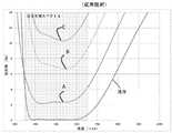
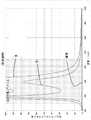
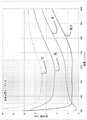
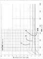
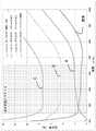
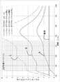
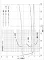
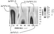
図5A~5Cは、清浄な状態におけるモデル比較例1および2の被覆表面、並びに表面欠陥条件A、BおよびCの、モデル比較例1および2の被覆表面の、垂直入射でのモデル反射率の変化を示している。図5Aに示されるように、モデル比較例1の被覆表面の反射率は、表面厚の除去が増加するに連れて増加する。詳しくは、清浄な状態における反射率は、約425nmから約650nmの範囲の可視スペクトル内で約0.5%未満であり、表面欠陥条件Cの後での反射率は、同じ可視スペクトル範囲内で、100nmの表面厚の除去で、約10.5%超であり、これは、約10%の絶対反射率の増加である。このように、表面欠陥のない、反射防止コーティングの残りと比べた場合、表面欠陥の視認性は増加している。図5Bは、異なる表面厚の除去後の、モデル比較例1のコントラスト比を示している。コントラスト比は、より大きい表面厚が除去されるにつれて、著しく増加し、約400nmから約700nmの範囲の可視スペクトルに亘り、約15超および約45超のコントラスト比の値が観察される。図5Cは、モデル比較例2のコントラスト比を示しており、サファイア基体が使用された場合、表面欠陥の視認性がさらにより著しくなる(小さい表面厚でさえ)ことを示している。 5A-5C show the model reflectance at normal incidence of the coated surfaces of Model Comparative Examples 1 and 2 in the clean state, and of the coated surfaces of Model Comparative Examples 1 and 2 under surface defect conditions A, B, and C. showing change. As shown in FIG. 5A, the reflectance of the coated surface of Model Comparative Example 1 increases as the surface thickness removal increases. Specifically, the reflectance in the clean state is less than about 0.5% within the visible spectrum ranging from about 425 nm to about 650 nm, and the reflectance after surface defect condition C is , at a surface thickness removal of 100 nm, is greater than about 10.5%, which is an increase in absolute reflectance of about 10%. Thus, the visibility of surface defects is increased when compared to the rest of the antireflective coating without surface defects. FIG. 5B shows the contrast ratio of Model Comparative Example 1 after removal of different surface thicknesses. The contrast ratio increases significantly as more surface thickness is removed, and contrast ratio values greater than about 15 and greater than about 45 are observed across the visible spectrum ranging from about 400 nm to about 700 nm. FIG. 5C shows the contrast ratio for Model Comparative Example 2 and shows that the visibility of surface defects becomes even more pronounced (even at small surface thicknesses) when a sapphire substrate is used.
図5Dは、異なる表面厚の除去および変化する入射照明角について、Δa*b*に関するモデル色変化を示している。約30nmから約70nm、および約100nmから110nmの範囲の表面厚の除去では、Δa*b*値は、約60度までの入射照明角で6を超え、約20度までの入射照明角で、9ほど高くに到達し得る。FIG. 5D shows the model color variation with respect to Δa* b* for different surface thickness removals and varying incident illumination angles. For removal of surface thicknesses ranging from about 30 nm to about 70 nm and from about 100 nm to 110 nm, the Δa* b* values are greater than 6 for incident illumination angles up to about 60 degrees, and It can reach as high as 9.
モデル例3
モデル例3は、表9に示された構造を有する物品であり、化学強化したABSガラス基体およびその基体上に配置された反射防止コーティングを備える。反射防止コーティングに配置された順序で、反射防止コーティングの材料、および各材料層の厚さが、表9に与えられている。Model example 3
Model Example 3 is an article having the structure shown in Table 9, comprising a chemically strengthened ABS glass substrate and an antireflective coating disposed on the substrate. The materials of the anti-reflection coating and the thickness of each material layer are given in Table 9, in the order in which they are arranged in the anti-reflection coating.

図6Aは、清浄な状態におけるモデル例3の被覆表面、並びに表面欠陥条件A、BおよびCを有するその被覆表面の、垂直入射でのモデル反射率の変化を示している。図6Aに示されるように、その反射率は、表面厚の除去が増加するに連れて増加する;しかしながら、反射率の増加は、モデル比較例1および2と比べると、減少している。清浄な状態において、反射率は、約400nmから約700nmの範囲の可視スペクトル内で、約1.2%である。反射率は、表面欠陥条件C(すなわち、100nmの表面厚の除去)の後に、同じ可視スペクトル範囲内で、約8%未満まで増加しており、これは、清浄な状態を上回る、6.8%の絶対反射率の増加である。モデル比較例1および2と比べた場合、100nmまでの表面厚の除去を含む、表面欠陥の視認性は、著しく低下しているであろう。図6Bは、異なる表面厚の除去後の、モデル例3のコントラスト比を示している。100nmまでの表面厚が除去された場合でさえ、約400nmから約700nmの範囲の可視スペクトルに亘り、6未満のコントラスト比値が観察され、これは、モデル比較例1および2に観察されたコントラスト比よりも著しく小さい。 FIG. 6A shows the model reflectance variation at normal incidence for the coated surface of Model Example 3 in the clean state and for that coated surface with surface defect conditions A, B and C. FIG. As shown in FIG. 6A, the reflectance increases as the surface thickness removal increases; however, the increase in reflectance decreases when compared to Model Comparative Examples 1 and 2. In clean conditions, the reflectance is about 1.2% in the visible spectrum ranging from about 400 nm to about 700 nm. The reflectance increases within the same visible spectral range to less than about 8% after surface defect condition C (i.e., 100 nm surface thickness removal), which is 6.8 above the clean condition. % absolute reflectance increase. Visibility of surface defects, including removal of up to 100 nm surface thickness, would be significantly reduced when compared to Model Comparative Examples 1 and 2. FIG. 6B shows the contrast ratio of model example 3 after removal of different surface thicknesses. Contrast ratio values of less than 6 were observed across the visible spectrum ranging from about 400 nm to about 700 nm, even when ~100 nm of surface thickness was removed, which is comparable to the contrast observed in model comparative examples 1 and 2. significantly smaller than the ratio.
図6Cは、異なる表面厚の除去後の、変化する入射照明角での、Δa*b*に関するモデル色変化を示している。最大の色変化(またはΔa*b*の最高値)は、約10nmから約20nm、および約110nmから約130nmの範囲の表面厚の除去の際に観察された。そのときのΔa*b*値は、約60度までの入射照明角で、約4から約6の範囲にある。他の入射照明角および表面厚の全てで、Δa*b*値は4未満である。FIG. 6C shows the model color change with respect to Δa* b* at varying incident illumination angles after removal of different surface thicknesses. The greatest color change (or highest value of Δa* b* ) was observed upon removal of surface thicknesses ranging from about 10 nm to about 20 nm and from about 110 nm to about 130 nm. The Δa* b* values then range from about 4 to about 6 for incident illumination angles up to about 60 degrees. The Δa* b* values are less than 4 for all other incident illumination angles and surface thicknesses.
モデル例4
モデル例4は、表10に示された構造を有する物品であり、サファイア基体およびその基体上に配置された反射防止コーティングを備える。反射防止コーティングに配置された順序で、反射防止コーティングの材料、および各材料層の厚さが、表10に与えられている。Model example 4
Model Example 4 is an article having the structure shown in Table 10, comprising a sapphire substrate and an antireflective coating disposed on the substrate. The materials of the anti-reflection coating and the thickness of each material layer are given in Table 10, in the order in which they are arranged in the anti-reflection coating.

図7Aは、清浄な状態におけるモデル例4の被覆表面、並びに表面欠陥条件A、BおよびCを有するその被覆表面の、垂直入射でのモデル反射率の変化を示している。図7Aに示されるように、その反射率は、表面厚の除去が増加するに連れて増加する;しかしながら、反射率の増加は、モデル比較例1および2と比べると、減少している。清浄な状態において、反射率は、約400nmから約700nmの範囲の可視スペクトル内で、約2.2%である。反射率は、表面欠陥条件C(すなわち、100nmの表面厚の除去)の後に、約400nmから約700nmの範囲の可視スペクトル内で、約7%未満に、約420nmから約700nmの範囲の可視スペクトル内で、約6%未満に、そして、約450nmから約700nmの範囲の可視スペクトル内で、約5.5%未満に増加している。この反射率の増加は、約4.8%未満の絶対反射率であり、わずかに狭い可視スペクトル範囲内で、約3.3%未満の絶対反射率である。モデル比較例1および2と比べた場合、100nmまでの表面厚の除去を含む、表面欠陥の視認性は、著しく低下しているであろう。図7Bは、異なる表面厚の除去後の、モデル例4のコントラスト比を示している。100nmまでの表面厚が除去された場合でさえ、約400nmから約700nmの範囲の可視スペクトルに亘り、3未満のコントラスト比値が観察され、これは、モデル比較例1および2に観察されたコントラスト比よりも著しく小さい。 FIG. 7A shows the model reflectance variation at normal incidence for the coated surface of Model Example 4 in the clean state and for that coated surface with surface defect conditions A, B and C. FIG. As shown in FIG. 7A, the reflectance increases as the surface thickness removal increases; however, the increase in reflectance decreases when compared to Model Comparative Examples 1 and 2. In clean conditions, the reflectance is about 2.2% in the visible spectrum ranging from about 400 nm to about 700 nm. Reflectance is less than about 7% in the visible spectrum ranging from about 400 nm to about 700 nm after surface defect condition C (i.e., 100 nm surface thickness removal) within the visible spectrum, and to less than about 5.5% within the visible spectrum ranging from about 450 nm to about 700 nm. This increase in reflectance is less than about 4.8% absolute reflectance, and within the slightly narrower visible spectral range, less than about 3.3% absolute reflectance. Visibility of surface defects, including removal of up to 100 nm surface thickness, would be significantly reduced when compared to Model Comparative Examples 1 and 2. FIG. 7B shows the contrast ratio of model example 4 after removal of different surface thicknesses. Contrast ratio values of less than 3 were observed across the visible spectrum ranging from about 400 nm to about 700 nm, even when ~100 nm of surface thickness was removed, which is comparable to the contrast observed in model comparative examples 1 and 2. significantly smaller than the ratio.
図7Cは、異なる入射照明角での、清浄な状態におけるモデル例4の被覆表面のモデル反射率の変化を示している。図7Dは、異なる表面厚の除去後の、変化する入射照明角での、モデル例4の被覆表面のΔa*b*に関するモデル色変化を示している。最大の色変化(またはΔa*b*の最高値)は、約10nmから30nm、約60nmから130nm、および約120nmから約135nmの範囲の表面厚の除去の際に観察された。そのときのΔa*b*値は、約40度までの入射照明角で、約2.5から約4.5の範囲にある。他の入射照明角および表面厚の全てで、Δa*b*値は2.5未満である。FIG. 7C shows the change in model reflectance of the coated surface of Model Example 4 in clean conditions at different incident illumination angles. FIG. 7D shows the model color change with respect to Δa* b* for the coated surface of Model Example 4 at varying incident illumination angles after removal of different surface thicknesses. The greatest color change (or highest value of Δa* b* ) was observed upon removal of surface thicknesses ranging from about 10 nm to 30 nm, from about 60 nm to 130 nm, and from about 120 nm to about 135 nm. The Δa* b* values then range from about 2.5 to about 4.5 at incident illumination angles up to about 40 degrees. At all other incident illumination angles and surface thicknesses, the Δa* b* values are less than 2.5.
モデル例5
モデル例5は、表11に示された構造を有する物品であり、化学強化したABSガラス基体およびその基体上に配置された反射防止コーティングを備える。反射防止コーティングに配置された順序で、反射防止コーティングの材料、および各材料層の厚さが、表11に与えられている。Model example 5
Model Example 5 is an article having the structure shown in Table 11, comprising a chemically strengthened ABS glass substrate and an antireflective coating disposed on the substrate. The materials of the anti-reflection coating and the thickness of each material layer are given in Table 11, in the order in which they are arranged in the anti-reflection coating.

図8Aは、清浄な状態におけるモデル例5の被覆表面、並びに表面欠陥条件A、BおよびCを有するその被覆表面の、垂直入射でのモデル反射率の変化を示している。図8Aに示されるように、その反射率は、表面厚の除去が増加するに連れて増加する;しかしながら、反射率の増加は、モデル比較例1および2と比べると、減少している。清浄な状態において、反射率は、約450nmから約700nmの範囲の可視スペクトル内で、約1%である。反射率は、表面欠陥条件C(すなわち、100nmの表面厚の除去)の後に、約400nmから約700nmの範囲の可視スペクトル内で、約8.5%未満に、そして約420nmから約700nmの範囲の可視スペクトル内で、約7.5%未満に増加している。この反射率の増加は、約7.5%未満の絶対反射率であり、わずかに狭い可視スペクトル範囲内で、約6.5%未満の絶対反射率である。モデル比較例1および2と比べた場合、100nmまでの表面厚の除去を含む、表面欠陥の視認性は、著しく低下しているであろう。図8Bは、異なる表面厚の除去後の、モデル例5のコントラスト比を示している。100nmまでの表面厚が除去された場合でさえ、約400nmから約700nmの範囲の可視スペクトルに亘り、9未満のコントラスト比値が観察され、これは、モデル比較例1および2に観察されたコントラスト比よりも著しく小さい。 FIG. 8A shows the model reflectance variation at normal incidence for the coated surface of Model Example 5 in the clean state and for that coated surface with surface defect conditions A, B and C. FIG. As shown in FIG. 8A, the reflectance increases as the surface thickness removal increases; however, the increase in reflectance decreases when compared to Model Comparative Examples 1 and 2. In clean conditions, the reflectance is about 1% in the visible spectrum ranging from about 450 nm to about 700 nm. Reflectance is less than about 8.5% in the visible spectrum in the range of about 400 nm to about 700 nm, and in the range of about 420 nm to about 700 nm after surface defect condition C (i.e., 100 nm surface thickness removal) within the visible spectrum of about 7.5%. This increase in reflectance is less than about 7.5% absolute reflectance and within the slightly narrower visible spectral range less than about 6.5% absolute reflectance. Visibility of surface defects, including removal of up to 100 nm surface thickness, would be significantly reduced when compared to Model Comparative Examples 1 and 2. FIG. 8B shows the contrast ratio of model example 5 after removal of different surface thicknesses. Contrast ratio values of less than 9 were observed across the visible spectrum ranging from about 400 nm to about 700 nm, even when ~100 nm of surface thickness was removed, which is comparable to the contrast observed in model comparative examples 1 and 2. significantly smaller than the ratio.
図8Cは、異なる入射照明角での、清浄な状態におけるモデル例5の被覆表面のモデル反射率の変化を示している。図8Dは、異なる表面厚の除去後の、変化する入射照明角での、モデル例5の被覆表面のΔa*b*に関するモデル色変化を示している。最大の色変化(またはΔa*b*の最高値)は、約10nmから約30nm、約60nmから約80nm、および約110nmから約120nmの範囲の表面厚の除去の際に観察された。そのときのΔa*b*値は、約60度までの入射照明角で、約3から約4.5の範囲にある。他の入射照明角および表面厚の全てで、Δa*b*値は3未満である。FIG. 8C shows the change in modeled reflectance of the coated surface of Model Example 5 in clean conditions at different incident illumination angles. FIG. 8D shows the model color change with respect to Δa* b* for the coated surface of Model Example 5 at varying incident illumination angles after removal of different surface thicknesses. The greatest color change (or highest value of Δa* b* ) was observed upon removal of surface thicknesses ranging from about 10 nm to about 30 nm, from about 60 nm to about 80 nm, and from about 110 nm to about 120 nm. The Δa* b* values then range from about 3 to about 4.5 for incident illumination angles up to about 60 degrees. The Δa* b* values are less than 3 for all other incident illumination angles and surface thicknesses.
理論により束縛する意図はないが、反射率スペクトルの平坦性からの意図的な逸脱または特定の色を与えるために、反射防止コーティングの1つ以上の層の厚さを調節することができる。例えば、モデル例5は、垂直入射での反射率スペクトルの平坦性からの意図的な逸脱を含み、これは、垂直入射での反射で見た場合、反射防止コーティングに青みがかった色を与える。このことは、ある用途において、恩恵であり得、例えば、1)層厚の製造上のばらつきにより生じる反射色のばらつきを小さく出来る、および2)図8Cおよび8Dに示されるように、60度などの視角から外れた角度での、比較的平坦な反射率スペクトルを可能にする。 While not intending to be bound by theory, the thickness of one or more layers of the antireflective coating can be adjusted to provide an intentional deviation from the flatness of the reflectance spectrum or a particular color. For example, Model Example 5 includes an intentional deviation from the flatness of the reflectance spectrum at normal incidence, which gives the antireflection coating a bluish color when viewed in reflection at normal incidence. This can be a benefit in certain applications, e.g., 1) less variation in reflected color caused by manufacturing variations in layer thickness, and 2) 60 degrees, etc., as shown in FIGS. 8C and 8D. allows for a relatively flat reflectance spectrum at angles off the viewing angle of .
1つ以上の実施の形態において、より大きい入射照明角(例えば、約60度超)での光学的性能は、ある場合には、反射防止コーティングへの追加の層の付加により、改善されることがあり、この追加の層の付加は、モデル例5に示されるような、800nm、900nm、またさらには1000nmまでなどの近IR波長に低振動波長域が延在することを可能にする。これにより、高入射照明角での、より低い振動およびより低い色座標がもたらされる。何故ならば、一般に、その物品の全反射率スペクトルは、より高い入射照明角で、より短い波長にシフトするからである。 In one or more embodiments, optical performance at larger incident illumination angles (eg, greater than about 60 degrees) is improved, in some cases by the addition of additional layers to the antireflective coating. and the addition of this additional layer allows the low vibrational wavelength range to extend into the near-IR wavelengths such as 800 nm, 900 nm, or even up to 1000 nm, as shown in Model Example 5. This results in lower vibration and lower color coordinates at high incident illumination angles. This is because the total reflectance spectrum of the article generally shifts to shorter wavelengths at higher incident illumination angles.
モデル例6
モデル例6は、表12に示された構造を有する物品であり、化学強化したABSガラス基体およびその基体上に配置された2つの反射防止コーティングを備える。一方の反射防止コーティングは、耐引掻性層(すなわち、2000nm厚のAlOxNy層)を備え、基体上に配置されている。第2の反射防止コーティングは、第1の反射防止コーティング上に配置されている。物品に配置された順序で、両方の反射防止コーティングに使用された材料、および各材料層の厚さが、表12に与えられている。Model example 6
Model Example 6 is an article having the structure shown in Table 12, comprising a chemically strengthened ABS glass substrate and two antireflective coatings disposed on the substrate. One antireflection coating comprises a scratch resistant layer (ie a 2000 nm thick AlOx Ny layer) and is placed on the substrate. A second antireflective coating is disposed on the first antireflective coating. The materials used for both anti-reflection coatings, and the thickness of each material layer, in the order in which they were placed on the article, are given in Table 12.

図9Aは、清浄な状態におけるモデル例6の被覆表面、並びに表面欠陥条件A、BおよびCを有するその被覆表面の、垂直入射でのモデル反射率の変化を示している。図9Aに示されるように、その反射率は、表面厚の除去が増加するに連れて増加する;しかしながら、反射率の増加は、モデル比較例1および2と比べると、減少している。清浄な状態において、反射率は、約400nmから約700nmの範囲の可視スペクトル内で、約1.5%から2%の範囲にある。反射率は、表面欠陥条件C(すなわち、100nmの表面厚の除去)の後に、同じ可視スペクトル内で、約7%未満に増加している。この反射率の増加は、約5.5%未満の絶対反射率である。モデル比較例1および2と比べた場合、100nmまでの表面厚の除去を含む、表面欠陥の視認性は、著しく低下しているであろう。図9Bは、異なる表面厚の除去後の、モデル例6のコントラスト比を示している。100nmまでの表面厚が除去された場合でさえ、約400nmから約700nmの範囲の可視スペクトルに亘り、5未満のコントラスト比値が観察され、これは、モデル比較例1および2に観察されたコントラスト比よりも著しく小さい。 FIG. 9A shows the model reflectance variation at normal incidence for the coated surface of Model Example 6 in the clean state and for that coated surface with surface defect conditions A, B and C. FIG. As shown in FIG. 9A, the reflectance increases as the surface thickness removal increases; however, the increase in reflectance decreases when compared to Model Comparative Examples 1 and 2. In clean conditions, the reflectance ranges from about 1.5% to 2% in the visible spectrum, which ranges from about 400 nm to about 700 nm. The reflectance increases to less than about 7% within the same visible spectrum after surface defect condition C (ie, 100 nm surface thickness removal). This reflectance increase is less than about 5.5% absolute reflectance. Visibility of surface defects, including removal of up to 100 nm surface thickness, would be significantly reduced when compared to Model Comparative Examples 1 and 2. FIG. 9B shows the contrast ratio of model example 6 after removal of different surface thicknesses. Contrast ratio values of less than 5 were observed across the visible spectrum ranging from about 400 nm to about 700 nm, even when ~100 nm of surface thickness was removed, which is comparable to the contrast observed in model comparative examples 1 and 2. significantly smaller than the ratio.
図9Cは、異なる入射照明角での、清浄な状態におけるモデル例6の被覆表面のモデル反射率の変化を示している。図9Dは、異なる入射照明角での、表面欠陥条件Bの後でのモデル例6の被覆表面の反射率の変化を示している。図9Eは、図9Dに示された被覆表面のコントラスト比を示している。図9Fは、異なる表面厚の除去に関する、変化する入射照明角での、Δa*b*に関する色変化を示している。最大の色変化(またはΔa*b*の最高値)は、約10nmから約30nm、約60nmから約80nm、および約110nmから約120nmの範囲の表面厚の除去の際に観察された。そのときのΔa*b*値は、約60度までの入射照明角で、約2.5から約3.5の範囲にある。他の入射照明角および表面厚の全てで、Δa*b*値は2.5未満である。FIG. 9C shows the change in model reflectance of the coated surface of Model Example 6 in clean conditions at different incident illumination angles. FIG. 9D shows the change in reflectance of the coated surface of model example 6 after surface defect condition B at different incident illumination angles. FIG. 9E shows the contrast ratio of the coated surface shown in FIG. 9D. FIG. 9F shows the color change with respect to Δa* b* at varying incident illumination angles for removal of different surface thicknesses. The greatest color change (or highest value of Δa* b* ) was observed upon removal of surface thicknesses ranging from about 10 nm to about 30 nm, from about 60 nm to about 80 nm, and from about 110 nm to about 120 nm. The Δa* b* values then range from about 2.5 to about 3.5 for incident illumination angles up to about 60 degrees. At all other incident illumination angles and surface thicknesses, the Δa* b* values are less than 2.5.
モデル比較例7
モデル比較例7は、モデル比較例1のような構造を有する物品である。図10A~10Bは、清浄な状態におけるモデル比較例7の被覆表面、並びに表面欠陥条件D、EおよびFを有するその被覆表面の、モデル反射率の変化を示しており、汚染物質は指紋擬似媒質である。図10Aは、清浄な状態におけるモデル比較例7の被覆表面、並びに異なる表面欠陥条件後の被覆表面の、反射率を示している。その反射率は、汚染物質の厚さが増加するに連れて増加する。詳しくは、清浄な状態において、反射率は、約425nmから約650nmの範囲の可視スペクトル内で、約0.5%未満である。表面欠陥条件D後の反射率は、同じ可視スペクトル範囲内で約9%超であり、表面欠陥条件EおよびF後の反射率は、可視スペクトルのより狭い範囲に亘り、約12%ほど大きい絶対反射率の振幅を有する振動を含み、最大反射率は、約12%より大きい。清浄な状態と表面欠陥D~Fとの間の反射率の増加は、約11.5%以上の絶対反射率とモデル化された。このように、表面欠陥の視認性は、表面欠陥のない、反射防止コーティングの残りと比べた場合、著しく増加している。図10Bは、表面欠陥条件D~Fの各々に関する、図10Aに示されたモデル構造のコントラスト比を示している。そのコントラスト比スペクトルは、約400nmから約700nmの範囲の可視スペクトルに亘り、著しく振動し、条件DおよびEに関して、100を超えている。Model comparison example 7
Comparative model example 7 is an article having a structure similar to that of comparative model example 1. 10A-10B show the change in model reflectance for the coated surface of Model Comparative Example 7 in the clean state and for that coated surface with surface defect conditions D, E and F, where the contaminant is a fingerprint simulating medium. is. FIG. 10A shows the reflectance of the coated surface of Model Comparative Example 7 in the clean state as well as the coated surface after different surface defect conditions. Its reflectivity increases as the thickness of the contaminant increases. Specifically, in a clean state, the reflectance is less than about 0.5% within the visible spectrum ranging from about 425 nm to about 650 nm. The reflectance after surface defect condition D is greater than about 9% within the same visible spectral range, and the reflectance after surface defect conditions E and F is approximately 12% greater absolute over a narrower range of the visible spectrum. It includes oscillations with amplitudes of reflectance, the maximum reflectance being greater than about 12%. The increase in reflectance between the clean condition and surface defects D through F was modeled as an absolute reflectance of approximately 11.5% or greater. Thus, the visibility of surface defects is significantly increased when compared to the rest of the antireflective coating without surface defects. FIG. 10B shows the contrast ratio of the model structure shown in FIG. 10A for each of surface defect conditions D-F. Its contrast ratio spectrum oscillates significantly over the visible spectrum ranging from about 400 nm to about 700 nm, exceeding 100 for conditions D and E.
モデル例8
モデル例8は、モデル例3と同じ構造を有する物品を含んだ。Model example 8
Model Example 8 included an article having the same construction as Model Example 3.
図11Aは、清浄な状態におけるモデル例8の被覆表面、並びに表面欠陥条件D、EおよびFを有するその被覆表面の、垂直入射でのモデル反射率の変化を示している。図11Aに示されるように、その反射率は、汚染物質の厚さが増加するに連れて増加する;しかしながら、反射率の増加は、モデル比較例7と比べると、減少している。清浄な状態において、反射率は、約400nmから約700nmの範囲の可視スペクトル内で、約1.2%である。反射率は、表面欠陥条件Dの後に、約400nmから約700nmの可視スペクトル範囲内で、約8%未満まで増加している。反射率は、表面欠陥条件Eの後に、約450nmから約700nmの可視スペクトル範囲内で、約8%未満まで増加している。反射率は、表面欠陥条件Fの後に、約425nmから約675nmの可視スペクトル範囲内で、約8.5%未満まで増加している。この反射率の増加は、約7.3%未満の絶対反射率である。モデル比較例7と比べた場合、2000nmまでの指紋擬似媒質の付加を含む表面欠陥の視認性は、著しく低下しているであろう。図11Bは、異なる厚さの指紋擬似媒質の付加後の、モデル例8のコントラスト比を示している。2000nmまでの厚さを有する指紋擬似媒質が被覆表面上に存在する場合でさえ、約400nmから約700nmの範囲の可視スペクトルに亘り、7.5未満のコントラスト比値が観察され、これは、モデル比較例7に観察されたコントラスト比よりも著しく小さい。 FIG. 11A shows the model reflectance variation at normal incidence for the coated surface of Model Example 8 in the clean state and for that coated surface with surface defect conditions D, E, and F. FIG. As shown in FIG. 11A, the reflectance increases as the contaminant thickness increases; however, the increase in reflectance decreases when compared to Model Comparative Example 7. In clean conditions, the reflectance is about 1.2% in the visible spectrum ranging from about 400 nm to about 700 nm. The reflectance increases to less than about 8% in the visible spectral range from about 400 nm to about 700 nm after surface defect condition D. The reflectance increases to less than about 8% in the visible spectral range from about 450 nm to about 700 nm after surface defect condition E. The reflectance increases to less than about 8.5% in the visible spectral range from about 425 nm to about 675 nm after surface defect condition F. This reflectance increase is less than about 7.3% absolute reflectance. When compared to Model Comparative Example 7, the visibility of surface defects, including the addition of fingerprint simulating media up to 2000 nm, would be significantly reduced. FIG. 11B shows the contrast ratio of Model Example 8 after the addition of fingerprint simulating media of different thicknesses. Contrast ratio values of less than 7.5 are observed across the visible spectrum ranging from about 400 nm to about 700 nm, even when a fingerprint simulating medium with a thickness of up to 2000 nm is present on the coated surface, which is consistent with the model Significantly lower than the contrast ratio observed in Comparative Example 7.
モデル例9
モデル例9は、モデル例4と同じ構造を有する物品を含んだ。Model example 9
Model Example 9 included an article having the same construction as Model Example 4.
図12Aは、清浄な状態におけるモデル例9の被覆表面、並びに表面欠陥条件D、EおよびFを有するその被覆表面の、垂直入射でのモデル反射率の変化を示している。図12Aに示されるように、その反射率は、汚染物質の厚さが増加するに連れて増加する;しかしながら、反射率の増加は、モデル比較例7と比べると、減少している。清浄な状態において、反射率は、約400nmから約700nmの範囲の可視スペクトル内で、約2.2%である。反射率は、表面欠陥条件Dの後に、約400nmから約700nmの可視スペクトル範囲内で、約6%未満まで増加している。反射率は、表面欠陥条件Eの後に、約450nmから約700nmの可視スペクトル範囲内で、約6%未満まで増加している。反射率は、表面欠陥条件Fの後に、約450nmから約700nmの可視スペクトル範囲内で、約6%未満まで増加している。この反射率の増加は、約3.8%未満の絶対反射率である。モデル比較例7と比べた場合、2000nmまでの指紋擬似媒質の付加を含む表面欠陥の視認性は、著しく低下しているであろう。図12Bは、異なる厚さの指紋擬似媒質の付加後の、モデル例9のコントラスト比を示している。2000nmまでの厚さを有する指紋擬似媒質が被覆表面上に存在する場合でさえ、約400nmから約700nmの範囲の可視スペクトルに亘り、3.3未満のコントラスト比値が観察され、これは、モデル比較例7に観察されたコントラスト比よりも著しく小さい。 FIG. 12A shows the variation in model reflectance at normal incidence for the coated surface of Model Example 9 in the clean state and for that coated surface with surface defect conditions D, E and F. FIG. As shown in FIG. 12A, the reflectance increases as the contaminant thickness increases; however, the increase in reflectance decreases when compared to Model Comparative Example 7. In clean conditions, the reflectance is about 2.2% in the visible spectrum ranging from about 400 nm to about 700 nm. The reflectance increases to less than about 6% in the visible spectral range from about 400 nm to about 700 nm after surface defect condition D. The reflectance increases to less than about 6% in the visible spectral range from about 450 nm to about 700 nm after surface defect condition E. Reflectance increases to less than about 6% in the visible spectral range from about 450 nm to about 700 nm after surface defect condition F. This reflectance increase is less than about 3.8% absolute reflectance. When compared to Model Comparative Example 7, the visibility of surface defects, including the addition of fingerprint simulating media up to 2000 nm, would be significantly reduced. FIG. 12B shows the contrast ratio of model example 9 after the addition of fingerprint simulating media of different thicknesses. Contrast ratio values of less than 3.3 are observed across the visible spectrum ranging from about 400 nm to about 700 nm, even when a fingerprint simulating medium with a thickness of up to 2000 nm is present on the coated surface, which is consistent with the model Significantly lower than the contrast ratio observed in Comparative Example 7.
モデル例10
モデル例10は、モデル例6と同じ構造を有する物品を含んだ。図13Aは、清浄な状態におけるモデル例10の被覆表面、並びに表面欠陥条件D、EおよびFを有するその被覆表面の、垂直入射でのモデル反射率の変化を示している。図13Aに示されるように、その反射率は、汚染物質の厚さが増加するに連れて増加する;しかしながら、反射率の増加は、モデル比較例7と比べると、減少している。清浄な状態において、反射率は、約400nmから約700nmの範囲の可視スペクトル内で、約1.5%から2%の範囲にある。反射率は、表面欠陥条件DおよびEの後に、同じ可視スペクトル範囲内で、約7.5%未満まで増加している。反射率は、表面欠陥条件Fの後に、同じ可視スペクトル範囲内で、約8%未満まで増加している。この反射率の増加は、約6.5%未満の絶対反射率である。モデル比較例7と比べた場合、2000nmまでの指紋擬似媒質の付加を含む表面欠陥の視認性は、著しく低下しているであろう。図13Bは、異なる厚さの指紋擬似媒質の付加後の、モデル例10のコントラスト比を示している。2000nmまでの厚さを有する指紋擬似媒質が被覆表面上に存在する場合でさえ、約400nmから約700nmの範囲の可視スペクトルに亘り、5.5未満のコントラスト比値が観察され、これは、モデル比較例7に観察されたコントラスト比よりも著しく小さい。Model example 10
Model Example 10 included an article having the same construction as Model Example 6. FIG. 13A shows the variation in model reflectance at normal incidence for the coated surface of model example 10 in the clean state and for that coated surface with surface defect conditions D, E and F. FIG. As shown in FIG. 13A, the reflectance increases as the contaminant thickness increases; however, the increase in reflectance decreases when compared to Model Comparative Example 7. In clean conditions, the reflectance ranges from about 1.5% to 2% in the visible spectrum, which ranges from about 400 nm to about 700 nm. The reflectance increases to less than about 7.5% within the same visible spectral range after surface defect conditions D and E. Reflectance increases to less than about 8% within the same visible spectral range after surface defect condition F. This reflectance increase is less than about 6.5% absolute reflectance. When compared to Model Comparative Example 7, the visibility of surface defects, including the addition of fingerprint simulating media up to 2000 nm, would be significantly reduced. FIG. 13B shows the contrast ratio of
モデル例11および12
反射防止コーティングが、清浄な状態にある場合と、表面欠陥を含む場合の、物品の反射率スペクトルを理解するために、例11~12でモデル化を使用した。このモデル化は、反射防止コーティングに使用されることのある様々な材料から形成された層、およびABSガラスの基体から収集した屈折率データに基づいた。反射防止コーティングの層は、真空蒸着により形成した。形成された層のいくつかは、異なる厚さ(例えば、100nmおよび2000nm)で形成されたSiO2、およびAlOxNyを含んだ。光学膜の形成層および基体の屈折率(波長の関数として)を、分光偏光解析法を使用して測定した。表13~15は、測定した屈折率および分散曲線を含む。次いで、このように測定した屈折率を使用して、モデル例11および12の反射率スペクトルを計算した。Model examples 11 and 12
Modeling was used in Examples 11-12 to understand the reflectance spectra of the article when the antireflective coating was in a clean state and when it contained surface defects. The modeling was based on refractive index data collected from ABS glass substrates and layers formed from various materials that are sometimes used in anti-reflection coatings. A layer of antireflection coating was formed by vacuum deposition. Some of the layers formed included SiO2 and AlOx Ny formed with different thicknesses (eg, 100 nm and 2000 nm). The refractive index (as a function of wavelength) of the forming layers of the optical film and the substrate was measured using spectroscopic ellipsometry. Tables 13-15 contain the measured refractive index and dispersion curves. The reflectance spectra of model examples 11 and 12 were then calculated using the refractive indices thus measured.


モデル例11は、表16に示された構造を有する物品であり、化学強化したABSガラス基体およびその基体上に配置された反射防止コーティングを備える。反射防止コーティングに配置された順序で、反射防止コーティングの材料、および各材料層の厚さが、表16に与えられている。 Model Example 11 is an article having the structure shown in Table 16, comprising a chemically strengthened ABS glass substrate and an antireflective coating disposed on the substrate. The materials of the anti-reflection coating and the thickness of each material layer are given in Table 16, in the order in which they are arranged in the anti-reflection coating.

図14Aは、異なる入射照明角での、清浄な状態におけるモデル例11の被覆表面のモデル反射率の変化を示している。図14Bは、10度の観察角での、D65光源およびF2光源の下での、被覆表面の反射におけるa*およびb*色座標を示している。FIG. 14A shows the change in model reflectance of the coated surface of model example 11 in clean conditions at different incident illumination angles. FIG. 14B shows the a* and b* color coordinates in the reflection of the coated surface under D65 and F2 illuminants at a viewing angle of 10 degrees.
モデル例12は、表17に示された構造を有する物品であり、化学強化したABSガラス基体およびその基体上に配置された反射防止コーティングを備える。反射防止コーティングに配置された順序で、反射防止コーティングの材料、および各材料層の厚さが、表17に与えられている。 Model Example 12 is an article having the structure shown in Table 17, comprising a chemically strengthened ABS glass substrate and an antireflective coating disposed on the substrate. The materials of the anti-reflection coating and the thickness of each material layer are given in Table 17, in the order in which they are arranged in the anti-reflection coating.

図15Aは、異なる入射照明角での、清浄な状態におけるモデル例12の被覆表面のモデル反射率の変化を示している。図15Bは、10度の観察角での、D65光源およびF2光源の下での、被覆表面の反射におけるa*およびb*色座標を示している。FIG. 15A shows the change in model reflectance of the coated surface of model example 12 in clean conditions at different incident illumination angles. FIG. 15B shows the a* and b* color coordinates in the reflection of the coated surface under D65 and F2 illuminants at a viewing angle of 10 degrees.
表面厚の除去を含む表面欠陥が評価されている、これらの例により示されるように、表面厚が0nmから約150nmに増加するにつれて、図に示されるように、反射率は増加する傾向にあり、反射色も連続的にまたは準連続的に変化する。どの表面厚の除去でも、反射率、コントラスト比、または色ずれにおいて不連続的な飛びは観察されなかった。 As shown by these examples where surface defects including surface thickness removal have been evaluated, reflectance tends to increase as surface thickness increases from 0 nm to about 150 nm, as shown in the figure. , the reflected color also changes continuously or quasi-continuously. No discontinuity jumps in reflectance, contrast ratio, or color shift were observed with removal of any surface thickness.
理論により束縛する意図はないが、指紋液滴の付加の表面欠陥を有する1つ以上の実施の形態によるいくつかの反射防止コーティングのより低い絶対反射率(同じ指紋残留物を有する従来の反射防止コーティングにおいて観察されたより高い反射率と比べた場合)は、図11A~B、12A~Bおよび13A~Bに示されるように、指紋残留物と従来の反射防止コーティングとの間の界面と比べたときの、指紋液滴と1つ以上の実施の形態による反射防止コーティングとの間の界面でのより低い反射率により説明されるであろうと考えられる。言い方を変えれば、従来の反射防止コーティングは、空気に対してより完全にインピーダンス整合されているので、指紋の油分に対して、それほど完全にインピーダンス整合されていない。1つ以上の実施の形態による反射防止コーティングは、空気に対してそれほど完全にインピーダンス整合されていないが、それらは、従来の反射防止コーティングと比べて、両方とも、被覆表面上に配置され、空気に囲まれた、有限厚(例えば、約100nmから約2000nm)を有する指紋液滴を含む表面欠陥と組み合わされた場合、指紋の油分に対してより完全にインピーダンス整合され得、より低い全反射率を生じる。 While not intending to be bound by theory, the lower absolute reflectance of some antireflective coatings according to one or more embodiments with the additional surface imperfections of fingerprint droplets (conventional antireflective coatings with the same fingerprint residue) 11A-B, 12A-B and 13A-B, compared to the interface between fingerprint residue and conventional anti-reflection coatings. It is believed that this may be explained by the lower reflectance at the interface between the fingerprint droplet and the anti-reflective coating according to one or more embodiments. In other words, conventional anti-reflective coatings are less perfectly impedance-matched to fingerprint oil than they are to air because they are more perfectly impedance-matched to air. Although the anti-reflection coatings according to one or more embodiments are not so perfectly impedance-matched to air, they are both located on the coated surface and are more sensitive to air than conventional anti-reflection coatings. can be more perfectly impedance-matched to fingerprint oils, resulting in lower total reflectance produces
理論により束縛する意図はないが、ここに記載された反射防止コーティングのいくつかの実施の形態は、ある可視波長でより高い反射率を示すかもしれない;しかしながら、系レベルでは(すなわち、ディスプレイまたは電子機器の他の要素と組み合わされた場合)、反射率のこの増加は、構成部材レベル(すなわち、ディスプレイまたは電子機器の他の要素を持たない物品における)で現れるよりも、著しくないことがある。詳しくは、ディスプレイにおいて、カバー材料が直接接着剤で結合されたものでさえ、約0.5%から約3%の範囲の埋没表面反射が一般的である。約2%の埋没表面反射を有するディスプレイ装置は、反射率が0.1%の従来の反射防止コーティングと組み合わされた場合、約2.1%の全反射率を有する。したがって、同じディスプレイ装置は、反射率が1.2%の1つ以上の実施の形態による反射防止コーティングと組み合わされた場合、3.2%の全反射率を有する。この差は比較的小さく、両方のコーティングは、どのような反射防止コーティングも持たない同じディスプレイ系よりも、実質的に低い反射率を与えるであろう(すなわち、未被覆ガラスは約6%の反射率を示し、未被覆サファイアは約10%の反射率を示す)。 While not intending to be bound by theory, some embodiments of the antireflective coatings described herein may exhibit higher reflectance at certain visible wavelengths; however, at the system level (i.e., display or combined with other elements of the electronics), this increase in reflectance may not be as significant as it would appear at the component level (i.e., in an article without a display or other elements of the electronics). . Specifically, buried surface reflections in the range of about 0.5% to about 3% are common in displays, even with direct adhesive bonded cover materials. A display device with a buried surface reflection of about 2% has a total reflectance of about 2.1% when combined with a conventional anti-reflection coating with a reflectance of 0.1%. Thus, the same display device has a total reflectance of 3.2% when combined with an anti-reflection coating according to one or more embodiments with a reflectance of 1.2%. This difference is relatively small and both coatings will give substantially lower reflectance than the same display system without any anti-reflective coating (i.e. the uncoated glass has about 6% reflectance). reflectance, and uncoated sapphire exhibits a reflectance of about 10%).
ここに記載された反射防止コーティングの設計は、異なるサイズの表面欠陥または屈折率を有する表面欠陥に適合するように調節することができる。例えば、本発明の精神から逸脱せずに、層の厚さを調節することができる。一例において、反射防止コーティングは、厚さが2000nmの耐引掻性層を含んでも差し支えない;しかしながら、この層は、より薄く(例えば、約100nmから約2000nmの範囲)作ってもよく、それでも、物品が、アスファルト、コンクリートなどの硬質表面、または紙やすり上に落とされたときなどの、落下事象を潜在的に含む、引っ掻き、摩耗、または損傷事象に対するある程度の抵抗を与えるであろう。他の例において、耐引掻性層は、より厚く(例えば、約2000nmから約10000nm厚の範囲)作ることもできる。反射防止コーティングの上層(これらの例においてSiO2を含む)は、様々な厚さを有し得る。1つの実施の形態において、その厚さは、約1nmから約200nmの範囲にある。SiO2上層は、液体堆積または気相堆積手段により形成されるであろう、フルオロシラン層、アルキルシラン層、シルセスキオキサン層などを含む、シラン系低摩擦コーティング層などの、反射防止コーティング上に配置された追加のコーティングとの適合性も与えることができる。The design of the antireflective coatings described herein can be adjusted to accommodate surface defects of different sizes or having refractive indices. For example, layer thicknesses can be adjusted without departing from the spirit of the invention. In one example, the antireflective coating can include a scratch resistant layer with a thickness of 2000 nm; however, this layer can be made thinner (eg, in the range of about 100 nm to about 2000 nm) and still The article will provide some resistance to scratching, abrasion, or damage events, potentially including drop events, such as when dropped onto a hard surface such as asphalt, concrete, or sandpaper. In other examples, the scratch resistant layer can be made thicker (eg, in the range of about 2000 nm to about 10000 nm thick). The top layer of the anti-reflection coating (comprisingSiO2 in these examples) can have various thicknesses. In one embodiment, its thickness ranges from about 1 nm to about 200 nm. TheSiO2 top layer is on antireflective coatings such as silane-based low-friction coating layers, including fluorosilane layers, alkylsilane layers, silsesquioxane layers, etc., which may be formed by liquid deposition or vapor phase deposition means. Compatibility with additional coatings placed on the substrate can also be provided.
本発明の精神または範囲から逸脱せずに、様々な改変および変更を行えることが、当業者に明白であろう。 It will be apparent to those skilled in the art that various modifications and changes can be made without departing from the spirit or scope of the invention.
以下、本発明の好ましい実施形態を項分け記載する。 Hereinafter, preferred embodiments of the present invention will be described itemized.
実施形態1
基体表面を有する基体と、
被覆表面を形成する、前記基体表面上に配置された反射防止コーティングと、
を備えた物品であって、
前記被覆表面は、可視スペクトルに亘り、該被覆表面が清浄な状態にある場合の第1の平均反射率、および前記反射防止コーティングの約20nmから約500nmの表面厚が該被覆表面から除去された後の第2の平均反射率を示し、これにより、約0.5から約50の範囲のコントラスト比(前記第2の平均反射率:前記第1の平均反射率)が与えられ、前記反射防止コーティングの厚さは前記表面厚より大きく、前記反射率はCIE光源下で測定される、物品。
a substrate having a substrate surface;
an antireflective coating disposed on the substrate surface forming a coated surface;
An article comprising
The coated surface spans the visible spectrum, has a first average reflectance when the coated surface is in a clean state, and a surface thickness of about 20 nm to about 500 nm of the antireflective coating has been removed from the coated surface. Figure 2 shows a second average reflectance after, which provides a contrast ratio (said second average reflectance: said first average reflectance) in the range of about 0.5 to about 50; An article, wherein the thickness of the coating is greater than the surface thickness and the reflectance is measured under a CIE light source.
実施形態2
前記第1の平均反射率が、約450nmから約650nmの範囲の可視スペクトルの少なくとも一部に亘り約0.6%から約6.0%の範囲にあり、前記第2の平均反射率が、前記可視スペクトルに亘り約8%以下である、実施形態1に記載の物品。
wherein the first average reflectance ranges from about 0.6% to about 6.0% over at least a portion of the visible spectrum ranging from about 450 nm to about 650 nm, and the second average reflectance comprises: 2. The article of
実施形態3
前記反射防止コーティングが、前記基体表面上に配置された第1の層および該第1の層上に配置された、層厚を有する第2の層を備え、前記表面厚が、前記第2の層の層厚以上である、実施形態1または2に記載の物品。
The antireflective coating comprises a first layer disposed on the substrate surface and a second layer disposed on the first layer and having a layer thickness, wherein the surface thickness is equal to the second layer. 3. The article of
実施形態4
前記被覆表面が、該被覆表面が清浄な状態にある場合の第1の反射率、および前記反射防止コーティングの表面厚が該被覆表面から除去された後の第2の反射率を示し、該第1の反射率および該第2の反射率の少なくとも一方が、前記可視スペクトルに亘り、約2%以下の絶対反射率の平均振動振幅を示す、実施形態1から3いずれか1つに記載の物品。
the coated surface exhibiting a first reflectance when the coated surface is in a clean state and a second reflectance after a surface thickness of the antireflective coating is removed from the coated surface; 4. The article of any one of embodiments 1-3, wherein at least one of one reflectance and the second reflectance exhibits an average vibrational amplitude of absolute reflectance of about 2% or less over the visible spectrum. .
実施形態5
前記可視スペクトル内の約100nmの波長幅に亘り、前記第1の反射率および該第2の反射率の少なくとも一方が、約2%以下の絶対反射率の最大振動振幅を示す、実施形態4に記載の物品。
5. According to
実施形態6
前記反射率が、約0度から約60度の範囲の入射照明角で測定される、実施形態1から5いずれか1つに記載の物品。
6. The article of any one of embodiments 1-5, wherein the reflectance is measured at incident illumination angles ranging from about 0 degrees to about 60 degrees.
実施形態7
前記第1の反射率および前記第2の反射率の少なくとも一方が、前記可視スペクトルに亘り、平均反射率値に対して、20%未満の反射率振動を示す、実施形態1から6いずれか1つに記載の物品。
7. Any one of embodiments 1-6, wherein at least one of the first reflectance and the second reflectance exhibits a reflectance oscillation of less than 20% relative to an average reflectance value across the visible spectrum Articles described in 1.
実施形態8
前記第2の平均反射率が約3%未満である、実施形態1から7いずれか1つに記載の物品。
8. The article of any one of embodiments 1-7, wherein the second average reflectance is less than about 3%.
実施形態9
前記表面厚が約25nmまでであり、前記第2の平均反射率が約6%以下であり、前記被覆表面が、前記可視スペクトルに亘り、約0.5から約10の範囲のコントラスト比(前記第2の平均反射率:前記第1の平均反射率)を示す、実施形態1から8いずれか1つに記載の物品。
The surface thickness is up to about 25 nm, the second average reflectance is about 6% or less, and the coated surface has a contrast ratio (the 9. The article of any one of embodiments 1-8, wherein the article exhibits a second average reflectance: said first average reflectance.
実施形態10
前記表面厚が約50nmまでであり、前記第2の平均反射率が約8%以下であり、前記被覆表面が、前記可視スペクトルに亘り、約0.5から約20の範囲のコントラスト比(前記第2の平均反射率:前記第1の平均反射率)を示す、実施形態1から9いずれか1つに記載の物品。
The surface thickness is up to about 50 nm, the second average reflectance is about 8% or less, and the coated surface has a contrast ratio (the 10. The article of any one of embodiments 1-9, wherein the article exhibits a second average reflectance: said first average reflectance.
実施形態11
前記表面厚が約500nmまでであり、前記第2の平均反射率が約12%以下であり、前記被覆表面が、前記可視スペクトルに亘り、約0.5から約50の範囲のコントラスト比(前記第2の平均反射率:前記第1の平均反射率)を示す、実施形態1から10いずれか1つに記載の物品。Embodiment 11
The surface thickness is up to about 500 nm, the second average reflectance is about 12% or less, and the coated surface has a contrast ratio (the 11. The article of any one of embodiments 1-10, wherein the article exhibits a second average reflectance: said first average reflectance.
実施形態12
前記被覆表面が、前記可視スペクトルに亘り、約10未満のコントラスト比(前記第2の平均反射率:前記第1の平均反射率)を示し、前記第1の平均反射率および前記第2の平均反射率が、約0度から約60度の範囲の入射照明角で測定される、実施形態1から11いずれか1つに記載の物品。
The coated surface exhibits a contrast ratio (the second average reflectance: the first average reflectance) of less than about 10 across the visible spectrum, and the first average reflectance and the second
実施形態13
前記コントラスト比が、前記可視スペクトルに亘り、絶対比の単位で約1以下の平均振幅を有する振動を示す、実施形態1から12いずれか1つに記載の物品。Embodiment 13
13. The article of any one of embodiments 1-12, wherein the contrast ratio exhibits oscillations having an average amplitude of about 1 or less in absolute ratio units across the visible spectrum.
実施形態14
前記光源がD65光源またはF2光源を含む、実施形態1から13いずれか1つに記載の物品。
14. The article of any one of embodiments 1-13, wherein the light source comprises a D65 light source or an F2 light source.
実施形態15
表面を有する基体と、
被覆表面を形成する、前記表面上に配置された反射防止コーティングと、
を備えた物品であって、
前記物品の前記被覆表面が、該物品が清浄な状態にある場合、約450から約650nmの範囲の可視スペクトルに亘り約0.6%から約6.0%の範囲にある第1の平均反射率、および前記被覆表面が、約100nmから約2000nmの範囲の厚さを有する指紋擬似媒質の層を含む場合、前記可視スペクトルに亘り約10%以下の第2の平均反射率を示し、前記指紋擬似媒質が1.4~1.6の屈折率を有する、物品。Embodiment 15
a substrate having a surface;
an antireflective coating disposed on the surface forming a coated surface;
An article comprising
the coated surface of the article has a first average reflectance in the range of about 0.6% to about 6.0% over the visible spectrum in the range of about 450 to about 650 nm when the article is in a clean state; and the coated surface exhibits a second average reflectance of less than or equal to about 10% across the visible spectrum when the coated surface comprises a layer of fingerprint simulating medium having a thickness ranging from about 100 nm to about 2000 nm; An article, wherein the quasi-medium has a refractive index between 1.4 and 1.6.
実施形態16
前記可視スペクトルに亘り、前記第2の平均反射率:前記第1の平均反射率の比が約20以下であり、該比が、絶対比の単位で約10以下の平均振幅の振動を示す、実施形態15に記載の物品。
Across the visible spectrum, the ratio of the second average reflectance to the first average reflectance is less than or equal to about 20, the ratio exhibiting oscillations with an average amplitude of less than or equal to about 10 in units of absolute ratio; 16. The article of embodiment 15.
実施形態17
前記被覆表面が、前記指紋擬似媒質の層を備え、前記可視スペクトルに亘り、約8%以下の絶対反射率の最大反射率値を有し、該被覆表面が、前記指紋擬似媒質の層を備え、前記可視スペクトルに亘り、約7.5%以下の絶対反射率の最大振動振幅を持つ反射率を有する、実施形態15または16に記載の物品。
The coated surface comprises a layer of the fingerprint simulating medium and has a maximum reflectance value of less than or equal to about 8% absolute reflectance across the visible spectrum, the coated surface comprising the layer of the fingerprint simulating medium. 17. The article of
実施形態18
基体表面を有する基体と、
被覆表面を形成する、前記基体表面上に配置された反射防止コーティングと、
を備えた物品であって、
前記被覆表面が、清浄な状態において、光源の下の垂直入射から約0度から約75度の範囲の入射照明角を使用して測定した場合の第1の色座標(a*1、b*1)、および前記被覆表面から、前記反射防止コーティングの約0.1nmから約140nmの範囲の表面厚を除去した後の前記光源の下の前記入射照明角を使用して測定した場合の第2の色座標(a*2、b*2)を示し、
Δa*b*が約6以下である、物品。
a substrate having a substrate surface;
an antireflective coating disposed on the substrate surface forming a coated surface;
An article comprising
A first color coordinate (a*1 , b*1 ), and second when measured using the incident illumination angle under the light source after removing from the coated surface a surface thickness of the antireflective coating in the range of about 0.1 nm to about 140 nm. indicates the color coordinates (a*2 , b*2 ) of
An article having a Δa* b* of about 6 or less.
実施形態19
前記被覆表面から約100nm以上の押込み深さに亘り、バーコビッチ圧子硬度試験により該被覆表面上で測定して、約5GPa以上の硬度を示す、実施形態18に記載の物品。Embodiment 19
19. The article of
実施形態20
前記入射照明角が約60度であり、前記表面厚が約0.1から約100nmの範囲にあり、Δa*b*が約3未満である、実施形態18または19に記載の物品。
20. The article of
10、100 物品
20、200 基体
22、220 表面
30、300 反射防止コーティング
32、320 被覆表面
34、340 表面欠陥
311 第1の層
312 第2の層
360 表面厚
365 汚染物質10, 100
Claims (10)
Translated fromJapanese被覆表面を形成する、前記基体表面上に配置された反射防止コーティングと、
を備えた物品であって、
前記被覆表面は、可視スペクトルに亘り、該被覆表面が清浄な状態にある場合の第1の平均反射率、および前記反射防止コーティングの20nmから500nmの表面厚が該被覆表面から除去された後の第2の平均反射率を示し、これにより、0.5から50の範囲のコントラスト比(前記第2の平均反射率:前記第1の平均反射率)が与えられ、前記反射防止コーティングの厚さは前記表面厚より大きく、前記反射率はCIE光源下で測定される、物品。a substrate having a substrate surface;
an antireflective coating disposed on the substrate surface forming a coated surface;
An article comprising
The coated surface has a first average reflectance over the visible spectrum when the coated surface is in a clean state and after a surface thickness of the antireflective coating of 20 nm to 500 nm has been removed from the coated surface. denoting a second average reflectance, which gives a contrast ratio (said second average reflectance: said first average reflectance) ranging from 0.5 to 50, and the thickness of said anti-reflection coating is greater than said surface thickness and said reflectance is measured under a CIE light source.
被覆表面を形成する、前記基体表面上に配置された反射防止コーティングと、
を備えた物品であって、
前記被覆表面は、可視スペクトルに亘り、該被覆表面が清浄な状態にある場合の第1の反射率、および前記被覆表面に、100nmから2000nmの範囲の厚さを有し、1.4~1.6の屈折率を有する、材料または汚染物質が付加された場合の第2の反射率を示し、これにより、0.5から50の範囲のコントラスト比(前記第2の平均反射率:前記第1の平均反射率)が与えられ、前記反射防止コーティングの厚さは前記表面厚より大きく、前記反射率はCIE光源下で測定される、物品。a substrate having a substrate surface;
an antireflective coating disposed on the substrate surface forming a coated surface;
An article comprising
The coated surface has a first reflectance over the visible spectrum when the coated surface is in a clean state and a thickness at the coated surface ranging from 100 nm to 2000 nm, and having a thickness of 1.4 to 1 6 shows a second reflectance with the addition of a material or contaminant having an index of refraction of 0.6, resulting in a contrast ratio ranging from 0.5 to 50 (said second average reflectance: said second reflectance). an average reflectance of 1), the thickness of said anti-reflection coating is greater than said surface thickness, and said reflectance is measured under a CIE light source.
前記第1の低屈折率副層が、SiO2を含み、
前記第2の高屈折率副層が、SiuAlvOxNy、Ta2O5、Nb2O5、AlN、Si3N4、SiNX、AlOxNy、SiOxNy、HfO2、TiO2、ZrO2、Y2O3、Al2O3、およびMoO3、またはこれらの組み合わせを含む、請求項1~6のうちのいずれか1項に記載の物品。the antireflective coating comprises a first low refractive index sublayer and a second high refractive index sublayer;
said first low refractive index sublayer comprisingSiO2 ;
wherein thesecond high indexsublayerisSiuAlvOxNy ,Ta2O5 ,Nb2O5 ,AlN ,Si3N4,SiNx,AlOxNy,SiOxNy, 7. The article of anyone of claims 1-6, comprisingHfO2 ,TiO2 , ZrO2,Y2O3 ,Al2O3, andMoO3, or combinations thereof.
Applications Claiming Priority (3)
| Application Number | Priority Date | Filing Date | Title |
|---|---|---|---|
| US201462002466P | 2014-05-23 | 2014-05-23 | |
| US62/002,466 | 2014-05-23 | ||
| JP2020089683AJP7096858B2 (en) | 2014-05-23 | 2020-05-22 | Low-contrast anti-reflective article with reduced visibility of scratches and fingerprints |
Related Parent Applications (1)
| Application Number | Title | Priority Date | Filing Date |
|---|---|---|---|
| JP2020089683ADivisionJP7096858B2 (en) | 2014-05-23 | 2020-05-22 | Low-contrast anti-reflective article with reduced visibility of scratches and fingerprints |
Publications (1)
| Publication Number | Publication Date |
|---|---|
| JP2022123136Atrue JP2022123136A (en) | 2022-08-23 |
Family
ID=53373609
Family Applications (3)
| Application Number | Title | Priority Date | Filing Date |
|---|---|---|---|
| JP2016568004AActiveJP6746502B2 (en) | 2014-05-23 | 2015-05-22 | Low-contrast anti-reflective article with reduced visibility of scratches and fingerprints |
| JP2020089683AActiveJP7096858B2 (en) | 2014-05-23 | 2020-05-22 | Low-contrast anti-reflective article with reduced visibility of scratches and fingerprints |
| JP2022101707ACeasedJP2022123136A (en) | 2014-05-23 | 2022-06-24 | Low-contrast antireflective article with reduced visibility of scratches and fingerprints |
Family Applications Before (2)
| Application Number | Title | Priority Date | Filing Date |
|---|---|---|---|
| JP2016568004AActiveJP6746502B2 (en) | 2014-05-23 | 2015-05-22 | Low-contrast anti-reflective article with reduced visibility of scratches and fingerprints |
| JP2020089683AActiveJP7096858B2 (en) | 2014-05-23 | 2020-05-22 | Low-contrast anti-reflective article with reduced visibility of scratches and fingerprints |
Country Status (7)
| Country | Link |
|---|---|
| US (3) | US10620344B2 (en) |
| EP (1) | EP3146368A1 (en) |
| JP (3) | JP6746502B2 (en) |
| KR (2) | KR102409481B1 (en) |
| CN (1) | CN106537190B (en) |
| TW (1) | TWI690723B (en) |
| WO (1) | WO2015179739A1 (en) |
Families Citing this family (22)
| Publication number | Priority date | Publication date | Assignee | Title |
|---|---|---|---|---|
| US9703011B2 (en) | 2013-05-07 | 2017-07-11 | Corning Incorporated | Scratch-resistant articles with a gradient layer |
| US9110230B2 (en) | 2013-05-07 | 2015-08-18 | Corning Incorporated | Scratch-resistant articles with retained optical properties |
| US9684097B2 (en) | 2013-05-07 | 2017-06-20 | Corning Incorporated | Scratch-resistant articles with retained optical properties |
| US9359261B2 (en) | 2013-05-07 | 2016-06-07 | Corning Incorporated | Low-color scratch-resistant articles with a multilayer optical film |
| US9366784B2 (en) | 2013-05-07 | 2016-06-14 | Corning Incorporated | Low-color scratch-resistant articles with a multilayer optical film |
| US9335444B2 (en) | 2014-05-12 | 2016-05-10 | Corning Incorporated | Durable and scratch-resistant anti-reflective articles |
| US11267973B2 (en) | 2014-05-12 | 2022-03-08 | Corning Incorporated | Durable anti-reflective articles |
| CN106537190B (en)* | 2014-05-23 | 2019-08-16 | 康宁股份有限公司 | The low contrast antireflective product of scratch and fingerprint visibility with reduction |
| US9790593B2 (en) | 2014-08-01 | 2017-10-17 | Corning Incorporated | Scratch-resistant materials and articles including the same |
| US10649588B2 (en) | 2014-10-14 | 2020-05-12 | Corning Incorporated | Piezoelectric film structures and sensors and display assemblies using same |
| JP2018536177A (en) | 2015-09-14 | 2018-12-06 | コーニング インコーポレイテッド | High light transmittance and scratch resistant anti-reflective article |
| DE102017105372B4 (en)* | 2017-03-14 | 2022-05-25 | Schott Ag | Transparent element with an anti-reflective coating and method of making same |
| US20190106805A1 (en)* | 2017-10-10 | 2019-04-11 | Wisconsin Alumni Research Foundation | Crystallization of amorphous multicomponent ionic compounds |
| TWI821234B (en) | 2018-01-09 | 2023-11-11 | 美商康寧公司 | Coated articles with light-altering features and methods for the production thereof |
| CN114085037B (en) | 2018-08-17 | 2023-11-10 | 康宁股份有限公司 | Inorganic oxide article with thin durable anti-reflective structure |
| WO2020069261A1 (en)* | 2018-09-28 | 2020-04-02 | Corning Incorporated | High hardness articles including an optical layer and methods for making the same |
| JP2022523261A (en)* | 2019-03-27 | 2022-04-21 | コーニング インコーポレイテッド | Optical coating of non-planar substrate and its manufacturing method |
| KR20220016883A (en) | 2019-06-05 | 2022-02-10 | 코닝 인코포레이티드 | Enhanced optical window for LIDAR application at 850-950 nm |
| CN110767668B (en)* | 2019-12-30 | 2020-03-27 | 杭州美迪凯光电科技股份有限公司 | CLCC package cover, package and camera module with nanoscale surface |
| US12147009B2 (en) | 2020-07-09 | 2024-11-19 | Corning Incorporated | Textured region to reduce specular reflectance including a low refractive index substrate with higher elevated surfaces and lower elevated surfaces and a high refractive index material disposed on the lower elevated surfaces |
| CN113702383A (en)* | 2021-07-14 | 2021-11-26 | 信利光电股份有限公司 | Apron quality testing equipment |
| JP2023167531A (en) | 2022-05-12 | 2023-11-24 | デクセリアルズ株式会社 | Optical multilayer body and article |
Citations (7)
| Publication number | Priority date | Publication date | Assignee | Title |
|---|---|---|---|---|
| US5847876A (en)* | 1996-06-25 | 1998-12-08 | Mcdonnell Douglas | Fingerprint resistant anti-reflection coatings |
| WO2000031569A1 (en)* | 1998-11-20 | 2000-06-02 | Sola International Holdings Ltd. | Coated lens to reduce visual perception of stains |
| JP2006302484A (en)* | 2004-07-22 | 2006-11-02 | Hitachi Maxell Ltd | Antireflection film, optical component for optical pickup, objective lens, and method for manufacturing optical component for optical pickup |
| JP2008096828A (en)* | 2006-10-13 | 2008-04-24 | Seiko Epson Corp | Optical article manufacturing method and optical article |
| JP2008096737A (en)* | 2006-10-12 | 2008-04-24 | Seiko Epson Corp | Plastic optical article and manufacturing method thereof |
| JP2009162989A (en)* | 2008-01-07 | 2009-07-23 | Hoya Corp | Antireflection film and optical component having the same, interchangeable lens and imaging device |
| JP2017518529A (en)* | 2014-05-23 | 2017-07-06 | コーニング インコーポレイテッド | Low contrast anti-reflective article with reduced scratch and fingerprint visibility |
Family Cites Families (40)
| Publication number | Priority date | Publication date | Assignee | Title |
|---|---|---|---|---|
| US4128303A (en)* | 1976-04-05 | 1978-12-05 | Kabushiki Kaisha Hoya Lens | Anti reflection coating with a composite middle layer |
| US4995684A (en) | 1986-06-18 | 1991-02-26 | Raytheon Company | Impact resistant and tempered optical elements |
| US4966437A (en)* | 1988-04-19 | 1990-10-30 | Litton Systems, Inc. | Fault-tolerant anti-reflective coatings |
| JP3333609B2 (en)* | 1993-10-28 | 2002-10-15 | 日東電工株式会社 | Method of removing oil film from anti-reflection layer |
| JPH0894805A (en)* | 1994-09-20 | 1996-04-12 | Olympus Optical Co Ltd | Production of optical film and optical element |
| US5719705A (en)* | 1995-06-07 | 1998-02-17 | Sola International, Inc. | Anti-static anti-reflection coating |
| US5948481A (en) | 1996-11-12 | 1999-09-07 | Yazaki Corporation | Process for making a optical transparency having a diffuse antireflection coating |
| JP2000171630A (en)* | 1998-12-04 | 2000-06-23 | Asahi Optical Co Ltd | Method for forming optical multilayer thin film |
| JP2003215309A (en)* | 2001-04-17 | 2003-07-30 | Sony Corp | Antireflection film and antireflection layer-affixed plastic substrate |
| US7445273B2 (en)* | 2003-12-15 | 2008-11-04 | Guardian Industries Corp. | Scratch resistant coated glass article resistant fluoride-based etchant(s) |
| DE102004027842A1 (en)* | 2004-06-08 | 2006-01-12 | Institut für Neue Materialien Gemeinnützige GmbH | Abrasion and scratch resistant low refractive index coatings on a substrate |
| JP4961100B2 (en) | 2004-06-30 | 2012-06-27 | 富士フイルム株式会社 | Antireflection film, polarizing plate, and image display device |
| US20070285776A1 (en) | 2004-08-12 | 2007-12-13 | Fujifilm Corporation | Anti-Reflection Film |
| WO2007097303A1 (en)* | 2006-02-27 | 2007-08-30 | Konica Minolta Opto, Inc. | Antireflection film, method for producing antireflection film, polarizing plate and display |
| JP2009122416A (en)* | 2007-11-15 | 2009-06-04 | Toppan Printing Co Ltd | Optical thin film |
| JP2009175226A (en)* | 2008-01-22 | 2009-08-06 | Fujifilm Corp | Optical film, polarizing plate, and image display device |
| WO2009131206A1 (en)* | 2008-04-24 | 2009-10-29 | 旭硝子株式会社 | Low reflection glass and protective plate for display |
| WO2010005578A1 (en) | 2008-07-11 | 2010-01-14 | Corning Incorporated | Glass with compressive surface for consumer applications |
| EP2321230A4 (en) | 2008-07-29 | 2012-10-10 | Corning Inc | Dual stage ion exchange for chemical strengthening of glass |
| JP2010167744A (en) | 2009-01-26 | 2010-08-05 | Sumitomo Osaka Cement Co Ltd | Product excellent in fingerprint resistance and manufacturing process thereof |
| JP2011017782A (en)* | 2009-07-07 | 2011-01-27 | Olympus Corp | Antireflective film |
| CN102024508B (en)* | 2009-09-14 | 2013-05-01 | 群康科技(深圳)有限公司 | Conducting plate structure |
| DE102009056594A1 (en)* | 2009-12-04 | 2011-06-09 | Q-Cells Se | Antireflection coating as well as solar cell and solar module |
| US8939606B2 (en)* | 2010-02-26 | 2015-01-27 | Guardian Industries Corp. | Heatable lens for luminaires, and/or methods of making the same |
| JP2012004349A (en)* | 2010-06-17 | 2012-01-05 | Az Electronic Materials Kk | Forming method of silicon oxynitride film and substrate with silicon oxynitride film manufactured using the same |
| TWI502617B (en)* | 2010-07-21 | 2015-10-01 | 應用材料股份有限公司 | Method,plasma processing apparatus ,and liner assembly for tuning electrical skews |
| DE102010048088A1 (en) | 2010-10-01 | 2012-04-05 | Carl Zeiss Vision Gmbh | Optical lens with scratch-resistant anti-reflection coating |
| US20120200816A1 (en)* | 2011-02-04 | 2012-08-09 | Guardian Industries Corp. | Electronic devices having reduced susceptibility to newton rings, and/or methods of making the same |
| US20120275026A1 (en)* | 2011-04-29 | 2012-11-01 | Unipixel Displays, Inc. | Low reflectance fingerprint resistant surface for displays |
| DE102011076754A1 (en)* | 2011-05-31 | 2012-12-06 | Schott Ag | Substrate element for the coating with an easy-to-clean coating |
| TWI588112B (en)* | 2011-11-30 | 2017-06-21 | 康寧公司 | Process for making of glass articles with optical and easy-to-clean coatings |
| EP3696293A1 (en) | 2011-11-30 | 2020-08-19 | Corning Incorporated | Optical coating method, apparatus and product |
| JP5181380B1 (en)* | 2012-01-10 | 2013-04-10 | ナルックス株式会社 | Optical multilayer film |
| CN104040379B (en) | 2012-01-10 | 2016-02-10 | 纳卢克斯株式会社 | Optical multilayer film |
| CN102850761B (en)* | 2012-09-26 | 2015-04-01 | 上海锦湖日丽塑料有限公司 | Scratch-resistant polycarbonate and preparation method thereof |
| JP2014071166A (en)* | 2012-09-28 | 2014-04-21 | Nippon Electric Glass Co Ltd | Optical member, and method of manufacturing the same |
| EP2906418B1 (en) | 2012-10-12 | 2021-05-26 | Corning Incorporated | Articles having retained strength |
| US9359261B2 (en) | 2013-05-07 | 2016-06-07 | Corning Incorporated | Low-color scratch-resistant articles with a multilayer optical film |
| US9703011B2 (en) | 2013-05-07 | 2017-07-11 | Corning Incorporated | Scratch-resistant articles with a gradient layer |
| CN103395247B (en) | 2013-07-30 | 2015-05-13 | 深圳欧菲光科技股份有限公司 | Cover plate glass and preparation method thereof |
- 2015
- 2015-05-22CNCN201580039267.4Apatent/CN106537190B/enactiveActive
- 2015-05-22TWTW104116507Apatent/TWI690723B/ennot_activeIP Right Cessation
- 2015-05-22KRKR1020167036042Apatent/KR102409481B1/enactiveActive
- 2015-05-22WOPCT/US2015/032138patent/WO2015179739A1/enactiveApplication Filing
- 2015-05-22KRKR1020227019584Apatent/KR102675982B1/enactiveActive
- 2015-05-22EPEP15728300.3Apatent/EP3146368A1/ennot_activeWithdrawn
- 2015-05-22USUS15/313,733patent/US10620344B2/enactiveActive
- 2015-05-22JPJP2016568004Apatent/JP6746502B2/enactiveActive
- 2020
- 2020-03-17USUS16/821,121patent/US11531141B2/enactiveActive
- 2020-05-22JPJP2020089683Apatent/JP7096858B2/enactiveActive
- 2022
- 2022-06-24JPJP2022101707Apatent/JP2022123136A/ennot_activeCeased
- 2022-11-09USUS17/983,527patent/US12092793B2/enactiveActive
Patent Citations (7)
| Publication number | Priority date | Publication date | Assignee | Title |
|---|---|---|---|---|
| US5847876A (en)* | 1996-06-25 | 1998-12-08 | Mcdonnell Douglas | Fingerprint resistant anti-reflection coatings |
| WO2000031569A1 (en)* | 1998-11-20 | 2000-06-02 | Sola International Holdings Ltd. | Coated lens to reduce visual perception of stains |
| JP2006302484A (en)* | 2004-07-22 | 2006-11-02 | Hitachi Maxell Ltd | Antireflection film, optical component for optical pickup, objective lens, and method for manufacturing optical component for optical pickup |
| JP2008096737A (en)* | 2006-10-12 | 2008-04-24 | Seiko Epson Corp | Plastic optical article and manufacturing method thereof |
| JP2008096828A (en)* | 2006-10-13 | 2008-04-24 | Seiko Epson Corp | Optical article manufacturing method and optical article |
| JP2009162989A (en)* | 2008-01-07 | 2009-07-23 | Hoya Corp | Antireflection film and optical component having the same, interchangeable lens and imaging device |
| JP2017518529A (en)* | 2014-05-23 | 2017-07-06 | コーニング インコーポレイテッド | Low contrast anti-reflective article with reduced scratch and fingerprint visibility |
Also Published As
| Publication number | Publication date |
|---|---|
| JP6746502B2 (en) | 2020-08-26 |
| EP3146368A1 (en) | 2017-03-29 |
| US20200217990A1 (en) | 2020-07-09 |
| JP2017518529A (en) | 2017-07-06 |
| KR102675982B1 (en) | 2024-06-17 |
| CN106537190A (en) | 2017-03-22 |
| KR102409481B1 (en) | 2022-06-16 |
| TWI690723B (en) | 2020-04-11 |
| US10620344B2 (en) | 2020-04-14 |
| WO2015179739A1 (en) | 2015-11-26 |
| US20230091466A1 (en) | 2023-03-23 |
| US12092793B2 (en) | 2024-09-17 |
| JP7096858B2 (en) | 2022-07-06 |
| KR20220084430A (en) | 2022-06-21 |
| TW201602624A (en) | 2016-01-16 |
| KR20170012391A (en) | 2017-02-02 |
| US20170199307A1 (en) | 2017-07-13 |
| JP2020126278A (en) | 2020-08-20 |
| US11531141B2 (en) | 2022-12-20 |
| CN106537190B (en) | 2019-08-16 |
Similar Documents
| Publication | Publication Date | Title |
|---|---|---|
| US12092793B2 (en) | Low contrast anti-reflection articles with reduced scratch and fingerprint visibility | |
| US12421398B2 (en) | Durable anti-reflective articles | |
| US11630244B2 (en) | Coatings of non-planar substrates and methods for the production thereof | |
| JP7292214B2 (en) | Reflective, pigmented, or color-shifting, scratch resistant coatings and articles | |
| JP6761348B2 (en) | Durable and scratch resistant anti-reflective article | |
| JP2023054069A (en) | Inorganic oxide articles with thin, durable anti-reflective structures | |
| US20240036236A1 (en) | Cover glass articles for camera lens and sensor protection and apparatus with the same | |
| JP2018536177A (en) | High light transmittance and scratch resistant anti-reflective article | |
| TWI856144B (en) | Low reflectance, anti-reflective film structures with controlled color and articles with the same |
Legal Events
| Date | Code | Title | Description |
|---|---|---|---|
| A521 | Request for written amendment filed | Free format text:JAPANESE INTERMEDIATE CODE: A523 Effective date:20220725 | |
| A621 | Written request for application examination | Free format text:JAPANESE INTERMEDIATE CODE: A621 Effective date:20220725 | |
| A977 | Report on retrieval | Free format text:JAPANESE INTERMEDIATE CODE: A971007 Effective date:20230508 | |
| A131 | Notification of reasons for refusal | Free format text:JAPANESE INTERMEDIATE CODE: A131 Effective date:20230517 | |
| A521 | Request for written amendment filed | Free format text:JAPANESE INTERMEDIATE CODE: A523 Effective date:20230817 | |
| A131 | Notification of reasons for refusal | Free format text:JAPANESE INTERMEDIATE CODE: A131 Effective date:20231004 | |
| A521 | Request for written amendment filed | Free format text:JAPANESE INTERMEDIATE CODE: A523 Effective date:20240104 | |
| A01 | Written decision to grant a patent or to grant a registration (utility model) | Free format text:JAPANESE INTERMEDIATE CODE: A01 Effective date:20240214 | |
| A045 | Written measure of dismissal of application [lapsed due to lack of payment] | Free format text:JAPANESE INTERMEDIATE CODE: A045 Effective date:20240626 |