JP2022113203A - Integrated circuit device and light source device - Google Patents
Integrated circuit device and light source deviceDownload PDFInfo
- Publication number
- JP2022113203A JP2022113203AJP2021009263AJP2021009263AJP2022113203AJP 2022113203 AJP2022113203 AJP 2022113203AJP 2021009263 AJP2021009263 AJP 2021009263AJP 2021009263 AJP2021009263 AJP 2021009263AJP 2022113203 AJP2022113203 AJP 2022113203A
- Authority
- JP
- Japan
- Prior art keywords
- power supply
- switching element
- supply voltage
- gate
- voltage
- Prior art date
- Legal status (The legal status is an assumption and is not a legal conclusion. Google has not performed a legal analysis and makes no representation as to the accuracy of the status listed.)
- Pending
Links
- 238000005086pumpingMethods0.000claimsdescription49
- 239000000872bufferSubstances0.000claimsdescription35
- 239000003990capacitorSubstances0.000claimsdescription27
- 230000003213activating effectEffects0.000claimsdescription7
- 230000003139buffering effectEffects0.000claimsdescription7
- 230000033228biological regulationEffects0.000description8
- 230000008878couplingEffects0.000description7
- 238000010168coupling processMethods0.000description7
- 238000005859coupling reactionMethods0.000description7
- 101100183118Solanum tuberosum 2MBCD geneProteins0.000description4
- 238000012986modificationMethods0.000description4
- 230000004048modificationEffects0.000description4
- 101100099988Arabidopsis thaliana TPD1 geneProteins0.000description3
- 101100352918Saccharomyces cerevisiae (strain ATCC 204508 / S288c) PTC1 geneProteins0.000description3
- 101100019424Solanum tuberosum IVD geneProteins0.000description3
- 230000006378damageEffects0.000description3
- 101100161168Saccharomyces cerevisiae (strain ATCC 204508 / S288c) TPD3 geneProteins0.000description2
- 239000004065semiconductorSubstances0.000description2
- 239000000758substrateSubstances0.000description2
- 239000000470constituentSubstances0.000description1
- 230000007423decreaseEffects0.000description1
- 230000000694effectsEffects0.000description1
- 230000003287optical effectEffects0.000description1
- 230000000630rising effectEffects0.000description1
Images


Classifications
- H—ELECTRICITY
- H05—ELECTRIC TECHNIQUES NOT OTHERWISE PROVIDED FOR
- H05B—ELECTRIC HEATING; ELECTRIC LIGHT SOURCES NOT OTHERWISE PROVIDED FOR; CIRCUIT ARRANGEMENTS FOR ELECTRIC LIGHT SOURCES, IN GENERAL
- H05B45/00—Circuit arrangements for operating light-emitting diodes [LED]
- H05B45/10—Controlling the intensity of the light
- H—ELECTRICITY
- H05—ELECTRIC TECHNIQUES NOT OTHERWISE PROVIDED FOR
- H05B—ELECTRIC HEATING; ELECTRIC LIGHT SOURCES NOT OTHERWISE PROVIDED FOR; CIRCUIT ARRANGEMENTS FOR ELECTRIC LIGHT SOURCES, IN GENERAL
- H05B45/00—Circuit arrangements for operating light-emitting diodes [LED]
- H05B45/30—Driver circuits
- H05B45/32—Pulse-control circuits
- H05B45/325—Pulse-width modulation [PWM]
- H—ELECTRICITY
- H05—ELECTRIC TECHNIQUES NOT OTHERWISE PROVIDED FOR
- H05B—ELECTRIC HEATING; ELECTRIC LIGHT SOURCES NOT OTHERWISE PROVIDED FOR; CIRCUIT ARRANGEMENTS FOR ELECTRIC LIGHT SOURCES, IN GENERAL
- H05B45/00—Circuit arrangements for operating light-emitting diodes [LED]
- H05B45/30—Driver circuits
- H05B45/37—Converter circuits
- H05B45/3725—Switched mode power supply [SMPS]
- Y—GENERAL TAGGING OF NEW TECHNOLOGICAL DEVELOPMENTS; GENERAL TAGGING OF CROSS-SECTIONAL TECHNOLOGIES SPANNING OVER SEVERAL SECTIONS OF THE IPC; TECHNICAL SUBJECTS COVERED BY FORMER USPC CROSS-REFERENCE ART COLLECTIONS [XRACs] AND DIGESTS
- Y02—TECHNOLOGIES OR APPLICATIONS FOR MITIGATION OR ADAPTATION AGAINST CLIMATE CHANGE
- Y02B—CLIMATE CHANGE MITIGATION TECHNOLOGIES RELATED TO BUILDINGS, e.g. HOUSING, HOUSE APPLIANCES OR RELATED END-USER APPLICATIONS
- Y02B20/00—Energy efficient lighting technologies, e.g. halogen lamps or gas discharge lamps
- Y02B20/30—Semiconductor lamps, e.g. solid state lamps [SSL] light emitting diodes [LED] or organic LED [OLED]
Landscapes
- Dc-Dc Converters (AREA)
- Circuit Arrangement For Electric Light Sources In General (AREA)
Abstract
Translated fromJapaneseDescription
Translated fromJapanese本発明は、集積回路装置及び光源装置等に関する。 The present invention relates to an integrated circuit device, a light source device, and the like.
特許文献1には、電源とグランドの間に直列に設けられた発光素子、N型トランジスター及びインダクターと、外部から入力されるPWM信号によりN型トランジスターをスイッチング制御する発光制御回路とを含む光源装置が開示されている。特許文献1の図21に示すように、N型トランジスターがオン又はオフに適切に制御されるように、N型トランジスターのゲートとソースの間にキャパシター及びダイオードの外付け部品が設けられている。
上記の外付け部品は、N型トランジスターがオン又はオフに適切に制御されるために必要であるが、一方で、ディスクリート部品として光源装置の回路基板に実装されるため、回路基板の面積又はコストを増加させる。このように、外付け部品の削減と、N型トランジスターがオン又はオフに適切に制御されることとを両立できないという課題がある。 The above external components are necessary for the N-type transistor to be properly controlled to be turned on or off. to increase Thus, there is a problem that it is not possible to achieve both a reduction in the number of externally attached parts and an appropriate ON/OFF control of the N-type transistor.
本開示の一態様は、電源ノードとインダクターの一端との間において発光素子のカソード側に前記発光素子に直列に設けられるスイッチング素子を制御する集積回路装置であって、前記スイッチング素子に駆動信号を出力し、前記駆動信号をアクティブにすることで前記スイッチング素子をオンさせ、前記駆動信号を非アクティブにすることで前記スイッチング素子をオフさせる駆動回路と、前記スイッチング素子であるトランジスターのソース電圧と同電位であるソース用電源電圧が入力され、前記ソース用電源電圧を基準とするゲート用電源電圧を生成するレギュレーターと、を含み、前記駆動回路は、前記ゲート用電源電圧と前記ソース用電源電圧に基づいてPWM信号をレベルシフトするレベルシフターを有し、前記レベルシフターの出力信号に基づく前記駆動信号を前記トランジスターのゲートに出力する集積回路装置に関係する。 One aspect of the present disclosure is an integrated circuit device that controls a switching element provided in series with the light emitting element on the cathode side of the light emitting element between a power supply node and one end of an inductor, wherein a drive signal is applied to the switching element. a driving circuit for turning on the switching element by activating the driving signal and turning off the switching element by deactivating the driving signal; and a regulator that receives a source power supply voltage that is a potential and generates a gate power supply voltage based on the source power supply voltage, wherein the drive circuit is adapted to the gate power supply voltage and the source power supply voltage. The present invention relates to an integrated circuit device having a level shifter for level-shifting a PWM signal based on the level shifter and outputting the drive signal based on the output signal of the level shifter to the gate of the transistor.
また本開示の他の態様は、上記に記載の集積回路装置と、前記発光素子と、前記スイッチング素子と、前記インダクターと、を含む光源装置に関係する。 Another aspect of the present disclosure relates to a light source device including the integrated circuit device described above, the light emitting element, the switching element, and the inductor.
以下、本開示の好適な実施形態について詳細に説明する。なお以下に説明する本実施形態は特許請求の範囲に記載された内容を不当に限定するものではなく、本実施形態で説明される構成の全てが必須構成要件であるとは限らない。 Preferred embodiments of the present disclosure are described in detail below. Note that the embodiments described below do not unduly limit the content described in the claims, and not all the configurations described in the embodiments are essential constituent elements.
1.外付け部品について
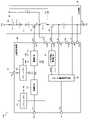
図1に、外付け部品を用いる場合における光源装置207の構成例を示す。光源装置207は、集積回路装置107と光源回路17とを含む。光源回路17を構成する各回路素子はディスクリート部品であり、それらのディスクリート部品は集積回路装置107と共に回路基板に実装される。1. Regarding External Components FIG. 1 shows a configuration example of the
光源回路17は、スイッチング素子11とアナログ調光スイッチング素子12とインダクター14と発光素子15と抵抗RCS、RISとキャパシターCAとダイオードDAとを含む。集積回路装置107は、駆動回路111とアナログ調光駆動回路121とを含む。 The
スイッチング素子11とアナログ調光スイッチング素子12はN型トランジスターである。発光素子15は、電流ILDによって駆動され、電流ILDの電流値に応じた明るさで発光する。発光素子15は、直列に接続された複数のレーザーダイオードである。但し、発光素子15は、1つのレーザーダイオードであってもよいし、或いはLED(Light Emitting Diode)であってもよい。 The
発光素子15とスイッチング素子11は、電源ノードNVIと第1ノードN1との間に直列に設けられる。電源ノードNVIは入力電源電圧VINが入力されるノードである。第1ノードN1は、スイッチング素子11であるN型トランジスターのソースであり、インダクター14の一端に接続される。インダクター14及びアナログ調光スイッチング素子12及び抵抗RISは、第1ノードN1とグランドノードNGNとの間に直列に設けられる。グランドノードNGNはグランド電圧GNDが入力されるノードである。キャパシターCAは電源ノードNVIと第1ノードN1との間に設けられる。ダイオードDAは、電源ノードNVIとインダクター14の他端との間に設けられる。
駆動回路111は、駆動信号GTAを出力することで、スイッチング素子11をオン又はオフに制御する。アナログ調光駆動回路121は、アナログ調光駆動信号GTBを出力することで、アナログ調光スイッチング素子12をオン又はオフに制御する。アナログ調光駆動回路121は、抵抗RCSの両端の電圧CSP、CSNと、抵抗RISの一端の電圧ISとに基づいて発光素子15に流れる電流ILDを一定に保つスイッチングレギュレート制御を行う。調光モードとして、例えばアナログ調光モードとPWM調光モードがある。アナログ調光モードにおいて、スイッチング素子11が常時オンしており、アナログ調光スイッチング素子12のスイッチングレギュレート制御によって発光素子15の発光量が制御される。また、PWM調光モードにおいて、スイッチング素子11がオンである期間ではアナログ調光スイッチング素子12がスイッチングレギュレート制御されることで発光素子15の発光量が一定に保たれるが、スイッチング素子11がオンオフすることで、そのオンデューティーによって発光素子15の発光量が制御される。 The
アナログ調光モードにおいて駆動信号GTAはハイレベルであり、また、PWM調光モードにおける比較的オンデューティーが長い場合において駆動信号GTAが長時間ハイレベルになる。このような場合において、スイッチング素子11のゲート電圧を適切に制御するために、光源回路17は、キャパシターCB、CCとダイオードDB、DDとツェナーダイオードDCと抵抗RAとを、外付け部品群19として含んでいる。 The drive signal GTA is at high level in the analog dimming mode, and is at high level for a long time when the on-duty is relatively long in the PWM dimming mode. In such a case, in order to appropriately control the gate voltage of the
抵抗RAとツェナーダイオードDCは、スイッチング素子11を保護するために設けられている。スイッチング素子11のソースである第1ノードN1は、インダクター14に流れる電流に応じた電圧となっており、グランド電圧ではない。このため、グランド電圧を基準とした駆動信号GTAを、キャパシターCBによりACカップリングしてスイッチング素子11のゲートに入力している。このとき、駆動信号GTAが長時間ハイレベルになると、抵抗RAによってスイッチング素子11のゲートソース間電圧が下がり、スイッチング素子11がオフしてしまう。 A resistor RA and a Zener diode DC are provided to protect the
これに対処するため、ダイオードDB、DD及びキャパシターCCが設けられている。アナログ調光駆動回路121が、スイッチングレギュレート用のアナログ調光駆動信号GTBと同様な信号GTB’をキャパシターCCの一端に出力することで、キャパシターCCの他端の電圧がスイッチング素子11のソース電圧を基準に変化し、その電圧がダイオードDDによってスイッチング素子11のゲートに伝達されることで、スイッチング素子11のゲート電圧がポンピングされる。 To address this, diodes DB, DD and capacitor CC are provided. The analog
以上のように、スイッチング素子11が意図せずオフしないように外付け部品群19が設けられているが、この外付け部品群19はディスクリート部品として光源装置207の回路基板に実装されるため、回路基板の面積又はコストを増加させる。このため、スイッチング素子11が意図せずオフしない構成としつつ、外付け部品を削減することが望まれる。 As described above, the
2.光源装置
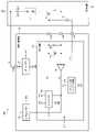
図2に、本実施形態における光源装置200の構成例を示す。光源装置200は、集積回路装置100と光源回路10とを含む。なお集積回路装置100を発光制御装置とも呼ぶ。2. Light Source Device FIG. 2 shows a configuration example of a
光源回路17は、スイッチング素子11とアナログ調光スイッチング素子12とインダクター14と発光素子15と抵抗RCS、RISとキャパシターCAとダイオードDAとを含む。集積回路装置107は、駆動回路111とアナログ調光駆動回路121とを含む。各回路素子の接続関係は図1で説明した通りであるが、本実施形態では外付け部品群19が省略される。なお、図2ではスイッチング素子11がN型トランジスターである例を説明するが、スイッチング素子11はPMOSトランジスターであってもよい。その場合の光源回路と集積回路装置の構成例については後述する。 The
集積回路装置100は、駆動回路110とアナログ調光駆動回路112と制御回路114とアナログ調光制御回路120とレギュレーター131、132とPWM端子TDCSと調光用電圧入力端子TACSと端子TVIN、TGTA、TVRL、TGTB、TIS、TCSP、TCSN、TGNDとを含む。レギュレーター131を第1レギュレーターとも呼び、レギュレーター132を第2レギュレーターとも呼ぶ。各端子は、集積回路装置の半導体基板に設けられるパッド、又は半導体基板を収容するパッケージの端子である。 The
端子TVRLは、スイッチング素子11のソースにACカップリングされることなく接続されており、端子TVRLには、スイッチング素子11のソース電圧と同電位のソース用電源電圧VRLが入力される。集積回路装置100の外部に設けられた電源回路から、端子TVINに入力電源電圧VINが入力され、端子TGNDにグランド電圧GNDが入力される。レギュレーター131は、ソース用電源電圧VRLと入力電源電圧VINを用いて、ソース用電源電圧VRLより所定電圧だけ高いゲート用電源電圧VRHを生成する。なお、ここではスイッチング素子11のソース電圧がソース用電源電圧VRLとしてレギュレーター131に入力される例を示したが、後述するように、スイッチング素子11のソース電圧がバッファリングされた後にソース用電源電圧としてレギュレーター131に入力されてもよい。 The terminal TVRL is connected to the source of the switching
レギュレーター132は、入力電源電圧VINを電源電圧VDRにレギュレートする。電源電圧VDRは、グランド電圧GNDを基準とする電圧であり、例えばソース用電源電圧VRLよりも低い電圧である。レギュレーター132は、例えば演算増幅器と抵抗等を用いたリニアレギュレーターである。
端子TGTAはACカップリングされることなくスイッチング素子11のゲートに接続される。駆動回路110は、PWM信号DCS’をレベルシフトするレベルシフターを有する。駆動回路110は、レベルシフト後の駆動信号GTAを、端子TGTAを介してスイッチング素子11のゲートに出力する。なお、駆動回路110の詳細構成例については後述するが、駆動回路110は、レベルシフターの出力信号をそのまま駆動信号GTAとして出力してもよいし、レベルシフターの出力信号をバッファリングした後に駆動信号GTAとして出力してもよい。PWM信号DCS’のローレベルはグランド電圧GNDであり、ハイレベルは制御回路114の電源電圧である。レベルシフト後の駆動信号GTAのローレベルはソース用電源電圧VRLであり、ハイレベルはゲート用電源電圧VRHである。スイッチング素子11がN型トランジスターである場合、駆動信号GTAがハイレベルのときスイッチング素子11がオンするので、ハイレベルがアクティブに相当し、ローレベルが非アクティブに相当する。 The terminal TGTA is connected to the gate of the switching
以上の本実施形態では、集積回路装置100はスイッチング素子11を制御する。スイッチング素子11は、電源ノードNVIとインダクター14の一端との間において発光素子15のカソード側に発光素子15と直列に設けられる。集積回路装置100は、駆動回路110とレギュレーター131とを含む。駆動回路110は、スイッチング素子11に駆動信号GTAを出力し、駆動信号GTAをアクティブにすることでスイッチング素子11をオンさせ、駆動信号GTAを非アクティブにすることでスイッチング素子11をオフさせる。レギュレーター131は、スイッチング素子11であるトランジスターのソース電圧と同電位であるソース用電源電圧VRLが入力され、ソース用電源電圧VRLを基準とするゲート用電源電圧VRHを生成する。駆動回路110は、ゲート用電源電圧VRHとソース用電源電圧VRLに基づいてPWM信号DCS’をレベルシフトするレベルシフターを有する。駆動回路110は、レベルシフターの出力信号に基づく駆動信号GTAをトランジスターのゲートに出力する。 In the present embodiment described above, the
本実施形態によれば、スイッチング素子11のゲートに入力される駆動信号GTAのローレベルがソース用電源電圧VRLとなり、ハイレベルが、ソース用電源電圧VRLを基準とするゲート用電源電圧VRHとなる。これにより、駆動信号GTAをACカップリングせずにスイッチング素子11のゲートに入力しても、スイッチング素子11が適切にオン又はオフに制御される。即ち、図1に示す光源回路17の外付け部品群19を設けることなく、スイッチング素子11を適切にオン又はオフに制御することが可能となる。 According to the present embodiment, the low level of the drive signal GTA input to the gate of the switching
以上、外付け部品群19を削減するための構成及び動作を説明した。以下、光源装置200のPWM調光モード及びアナログ調光モードに関する構成及び動作を説明する。 The configuration and operation for reducing the
PWM端子TDCSには、PWM調光モードにおいて調光制御に用いられるPWM信号DCSが、処理装置から入力される。調光用電圧入力端子TACSには、アナログ調光モードにおいて調光制御に用いられる調光用電圧ACSが、処理装置から入力される。処理装置は、集積回路装置100のホスト装置であり、例えばMPU、CPU等のプロセッサーである。 A PWM signal DCS used for dimming control in the PWM dimming mode is input from the processing device to the PWM terminal TDCS. A dimming voltage ACS used for dimming control in the analog dimming mode is input from the processing device to the dimming voltage input terminal TACS. A processing device is a host device of the
制御回路114は、PWM信号DCSをバッファリングし、バッファリング後のPWM信号DCS’を出力する。制御回路114はロジック回路であり、例えばインバーター等により構成されたバッファー回路である。駆動回路110は、制御回路114からのPWM信号DCS’に基づいて駆動信号GTAを出力する。 The
アナログ調光制御回路120は、調光用電圧ACS及びPWM信号DCSに基づいて制御信号CGTBを出力する。アナログ調光制御回路120は、PWM信号DCSがアクティブである期間において、アナログ調光スイッチング素子12をオン又はオフに制御する。具体的には、第1抵抗RCSの一端の電圧CSPが端子TCSPに入力され、第1抵抗RCSの他端の電圧CSNが端子TCSNに入力され、第2抵抗RISの一端の電圧ISが端子TISに入力される。アナログ調光制御回路120は、電圧CSP、CSN、ISと調光用電圧ACSに基づいて、発光素子15に流れる電流ILDをスイッチングレギュレート制御することで、調光用電圧ACSに対応した電流ILDとなるように制御する。 The analog
アナログ調光駆動回路112は、アナログ調光スイッチング素子12を駆動するドライバーである。アナログ調光駆動回路112は、アナログ調光制御回路120からの制御信号CGTBに基づいて、アナログ調光駆動信号GTBを、端子TGTBを介してアナログ調光スイッチング素子12のゲートに出力する。アナログ調光スイッチング素子12は、アナログ調光駆動信号GTBがアクティブのときオンであり、アナログ調光駆動信号GTBが非アクティブのときオフである。図2の例では、アナログ調光スイッチング素子12がN型トランジスターであり、ハイレベルがアクティブに相当し、ローレベルが非アクティブに相当する。 The analog dimming
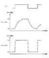
図3は、PWM調光モードにおける信号波形例である。PWM信号DCSの周期をTPWMとし、PWM信号DCSがハイレベルの期間をTHWとする。PWM信号DCSのデューティーは(THW/TPWM)×100%である。 FIG. 3 is an example of signal waveforms in the PWM dimming mode. Let TPWM be the period of the PWM signal DCS, and THW be the high-level period of the PWM signal DCS. The duty of the PWM signal DCS is (THW/TPWM)×100%.
PWM信号DCSがハイレベルのとき、駆動回路110はハイレベルの駆動信号GTAを出力する。本実施形態では、駆動信号GTAのハイレベルはゲート用電源電圧VRHである。これにより、スイッチング素子11がオンになる。このとき、アナログ調光制御回路120及びアナログ調光駆動回路112がアナログ調光スイッチング素子12をスイッチングすることで、スイッチングレギュレート制御を行う。これにより、調光用電圧ACSに対応した電流ILDが発光素子15に流れる。PWM信号DCSがローレベルのとき、駆動回路110はローレベルの駆動信号GTAを出力する。本実施形態では、駆動信号GTAのローレベルはソース用電源電圧VRLである。これにより、スイッチング素子11がオフになる。またアナログ調光制御回路120及びアナログ調光駆動回路112は、アナログ調光スイッチング素子12をオフにする。このとき、発光素子15に電流は流れない。発光素子15に流れる電流ILDの時間平均は、PWM信号DCSのデューティーによって決まるので、発光量もPWM信号DCSのデューティーによって決まる。このように、PWM調光モードでは、PWM信号DCSのデューティーにより調光制御される。 When the PWM signal DCS is at high level, the
なお、アナログ調光モードでは、常時ハイレベルのPWM信号DCSがPWM端子TDCSに入力される。アナログ調光モードにおける集積回路装置100の動作は、PWM調光モードにおいてPWM信号DCSがハイレベルであるときの集積回路装置100の動作と同様である。即ち、アナログ調光モードでは、調光用電圧ACSに対応した電流ILDが発光素子15に流れるので、調光用電圧ACSにより調光制御されることになる。 In the analog dimming mode, the PWM signal DCS which is always at high level is input to the PWM terminal TDCS. The operation of
以上の本実施形態では、集積回路装置100はアナログ調光駆動回路112を含む。アナログ調光駆動回路112は、アナログ調光スイッチング素子12にアナログ調光駆動信号GTBを出力する。アナログ調光スイッチング素子12は、インダクター14の他端からグランドノードNGNに流れる電流を制御する。アナログ調光駆動回路112は、駆動信号GTAがアクティブである期間において、アナログ調光駆動信号GTBをアクティブにすることでアナログ調光スイッチング素子12をオンさせ、アナログ調光駆動信号GTBを非アクティブにすることでアナログ調光スイッチング素子12をオフさせる。 In the present embodiment described above, the
本実施形態によれば、アナログ調光駆動回路112のスイッチングレギュレート制御により調光するアナログ調光モードと、駆動回路110のPWM駆動により調光するPWM調光モードと、を実現できる。アナログ調光モードにおいて、或いはPWM調光モードにおける比較的オンデューティーが長い場合において、スイッチング素子11が長時間オンになるが、本実施形態によれば、スイッチング素子11のゲートソース間電圧が低下しないので、図1で説明したような外付け部品群19を設けることなく、スイッチング素子11を適切にオン又はオフに制御できる。 According to this embodiment, an analog dimming mode for dimming by switching regulation control of the analog dimming
3.詳細構成例
図4に、光源装置200の第1詳細構成例を示す。なお、図4において、図2に示した構成要素の一部を省略しているが、それらの構成要素については図2と同様である。3. Detailed Configuration Example FIG. 4 shows a first detailed configuration example of the
第1詳細構成例では、駆動回路110は、ドライバー回路141とレベルシフター143とバッファーアンプ回路144と抵抗145とツェナーダイオード146とを含む。 In the first detailed configuration example, the
抵抗145の一端とツェナーダイオード146のアノードは端子TGTAに接続され、抵抗145の他端とツェナーダイオード146のカソードは端子TVRLに接続される。抵抗145とツェナーダイオード146は、スイッチング素子11の保護素子として設けられる。具体的には、集積回路装置100のシャットダウン時等において、スイッチング素子11であるN型トランジスターのゲートソース間電圧を0Vにしてスイッチング素子11をオフさせるために、抵抗145が設けられる。また、ゲートソース間電圧がN型トランジスターの耐圧を超えないようにツェナーダイオード146が設けられる。 One end of the
バッファーアンプ回路144は、スイッチング素子11のソース電圧をバッファリングし、バッファリング後の電圧をソース用電源電圧VRLとしてレギュレーター131に出力する。バッファーアンプ回路144は、例えばボルテージフォロア回路である。 The
レベルシフター143は、PWM信号DCS’を受けて、ハイレベルが電源電圧VDRであり且つローレベルがグランド電圧GNDである信号を生成し、その信号を、ハイレベルがゲート用電源電圧VRHであり且つローレベルがソース用電源電圧VRLである出力信号LSQにレベルシフトする。なお、PWM信号DCS’のローレベルはグランド電圧GNDであるが、ハイレベルは電源電圧VDRとは異なる電圧であってもよい。ドライバー回路141は、ソース用電源電圧VRLとゲート用電源電圧VRHを電源電圧として動作する。ドライバー回路141は、出力信号LSQをバッファリングし、バッファリング後の駆動信号GTAを、端子TGTAを介してスイッチング素子11のゲートに出力する。 The
図5に、光源装置200の第2詳細構成例を示す。なお、図5において、図2に示した構成要素の一部を省略しているが、それらの構成要素については図2と同様である。なお、第1詳細構成例と同様な部分については説明を適宜に省略する。 FIG. 5 shows a second detailed configuration example of the
第2詳細構成例では、集積回路装置100は端子TSPMPを含み、光源回路10はキャパシター18を含む。駆動回路110は、ポンピング用ドライバー回路142を含み、ドライバー回路141を含まない。 In the second detailed configuration example, the
レベルシフター143は、レベルシフト後の出力信号を駆動信号GTAとして出力する。この駆動信号GTAは、端子TGTAを介してスイッチング素子11のゲートに出力される。 The
キャパシター18の一端は、スイッチング素子11であるN型トランジスターのゲートに接続され、他端は、端子TSPMPに接続される。ポンピング用ドライバー回路142は、電源電圧VDRとグランド電圧GNDを電源として動作する。ポンピング用ドライバー回路142は、PWM信号DCS’を受けて、ハイレベルが電源電圧VDRであり且つローレベルがグランド電圧GNDであるポンピング用駆動信号SPMPを生成する。ポンピング用ドライバー回路142は、ポンピング用駆動信号SPMPを、端子TSPMPを介してキャパシター18の他端に出力する。ポンピング用駆動信号SPMPは、キャパシター18によりACカップリングされ、スイッチング素子11のゲートに入力される。 One end of the
図6に、第2詳細構成例における信号波形例を示す。「ポンピング無し」は、仮にポンピング用ドライバー回路142を設けなかった場合におけるスイッチング素子11のゲート電圧の波形を示す。「ポンピング有り」は、ポンピング用ドライバー回路142を設けた第2詳細構成例におけるスイッチング素子11のゲート電圧の波形を示す。 FIG. 6 shows an example of signal waveforms in the second detailed configuration example. "No pumping" indicates the waveform of the gate voltage of the switching
駆動信号GTAの電圧は、電源電圧VDR等と比べると比較的高い電圧であるため、例えばショート等による故障又は破壊を考慮すると、駆動信号GTAの駆動力は低い方が好ましい。本実施形態では、レベルシフター143が直接にスイッチング素子11のゲートを駆動することで、駆動力が低くなっている。しかし、レベルシフター143の駆動力が低いことから、仮にポンピング用ドライバー回路142を設けなかった場合には、駆動信号GTAの波形がなまってしまう。具体的には、PWM信号DCS’の立ち上がりエッジからゲート電圧がゲート用電源電圧VRHになるまでの時間が長くなるため、スイッチング素子11のオンデューティーが正しくなくなる等、スイッチング素子11が適切にオン又はオフに制御されなくなる。 Since the voltage of the drive signal GTA is relatively high compared to the power supply voltage VDR or the like, it is preferable that the driving power of the drive signal GTA is low in consideration of failure or destruction due to short circuit or the like. In this embodiment, the
第2詳細構成例では、ポンピング用ドライバー回路142がキャパシター18を介してスイッチング素子11のゲートをポンピングする。具体的には、ポンピング用ドライバー回路142がポンピング用駆動信号SPMPをグランド電圧GNDから電源電圧VDRにすることで、スイッチング素子11のゲートがソース用電源電圧VRLから電源電圧VDRだけ上がる。また、ポンピング用ドライバー回路142がポンピング用駆動信号SPMPを電源電圧VDRからグランド電圧GNDにすることで、スイッチング素子11のゲートがゲート用電源電圧VRHから電源電圧VDRだけ下がる。電源電圧VDRは、例えばゲート用電源電圧VRHとソース用電源電圧VRLの差分程度の電圧に設定されている。 In the second detailed configuration example, the pumping
図7に、光源装置200の第3詳細構成例を示す。なお、図7において、図2に示した構成要素の一部を省略しているが、それらの構成要素については図2と同様である。なお、第1詳細構成例又は第2詳細構成例と同様な部分については説明を適宜に省略する。 FIG. 7 shows a third detailed configuration example of the
第3詳細構成例では、第2詳細構成例に比べて、駆動回路110が更にドライバー回路141を含む。レベルシフター143よりも駆動力が高いドライバー回路141がスイッチング素子11のゲートを駆動すると共に、ポンピング用ドライバー回路142がスイッチング素子11のゲートをポンピングする。これにより、駆動信号GTAのエッジが更に急峻に変化する。 In the third detailed configuration example, the
図8に、光源装置200の第4詳細構成例を示す。なお、図8において、図2に示した構成要素の一部を省略しているが、それらの構成要素については図2と同様である。なお、第1詳細構成例、第2詳細構成例又は第3詳細構成例と同様な部分については説明を適宜に省略する。 FIG. 8 shows a fourth detailed configuration example of the
第4詳細構成例では、第3詳細構成例に比べて、駆動回路110がバッファーアンプ回路144を含まない。即ち、端子TVRLに入力されたソース電圧が直接的にソース用電源電圧VRLとしてレギュレーター131に入力される。ゲート用電源電圧VRHに関する消費電流は、レギュレーター131を介してインダクター14に流れる。しかし、その電流は、発光制御に大きな影響を与えない程度の電流量なので、バッファーアンプ回路144を省略することが可能である。 In the fourth detailed configuration example, the
なお、第1詳細構成例と第2詳細構成例においても、バッファーアンプ回路144が省略されてもよい。 Note that the
図9は、レギュレーター131の詳細構成例である。レギュレーター131は、電流源回路IBCとツェナーダイオードDICと抵抗RC1と抵抗RC2とN型トランジスターNTCとを含む。 FIG. 9 is a detailed configuration example of the
電流源回路IBCは、電源ノードNVIとツェナーダイオードDICのカソードとの間に設けられる。ツェナーダイオードDICのアノードはソース用電源電圧VRLのノードに接続される。電流源回路IBCがツェナーダイオードDICのカソードからアノードに電流を流すことで、ツェナーダイオードDICのカソードは、ソース用電源電圧VRLにツェナー電圧を加算した電圧となる。 Current source circuit IBC is provided between power supply node NVI and the cathode of Zener diode DIC. The anode of Zener diode DIC is connected to the node of source power supply voltage VRL. The current source circuit IBC causes a current to flow from the cathode of the Zener diode DIC to the anode, so that the cathode of the Zener diode DIC becomes a voltage obtained by adding the Zener voltage to the source power supply voltage VRL.
抵抗RC1と抵抗RC2は、ツェナーダイオードDICのカソードとアノードの間に直列接続される。N型トランジスターNTCのドレインは電源ノードNVIに接続され、ゲートは、抵抗RC1と抵抗RC2の間のノードに接続される。抵抗RC1と抵抗RC2が、ツェナーダイオードDICのカソードの電圧と、ソース用電源電圧VRLとの間を分圧し、その分圧電圧がN型トランジスターNTCのゲートに入力される。これにより、N型トランジスターNTCのソース電圧は、分圧電圧からN型トランジスターNTCの閾値電圧だけ低い電圧となり、その電圧がゲート用電源電圧VRHとして出力される。分圧電圧が、ソース用電源電圧VRLと所定電圧と閾値電圧とを加算した電圧付近となるように、抵抗RC1と抵抗RC2の分圧比が設定される。これにより、ゲート用電源電圧VRHは、ソース用電源電圧VRLよりも所定電圧だけ高い電圧となる。 Resistors RC1 and RC2 are connected in series between the cathode and anode of Zener diode DIC. The N-type transistor NTC has a drain connected to the power supply node NVI and a gate connected to a node between the resistors RC1 and RC2. The resistors RC1 and RC2 divide the voltage between the cathode voltage of the Zener diode DIC and the source power supply voltage VRL, and the divided voltage is input to the gate of the N-type transistor NTC. As a result, the source voltage of the N-type transistor NTC becomes a voltage lower than the divided voltage by the threshold voltage of the N-type transistor NTC, and this voltage is output as the gate power supply voltage VRH. The voltage dividing ratio of the resistors RC1 and RC2 is set so that the divided voltage is close to the sum of the source power supply voltage VRL, the predetermined voltage, and the threshold voltage. As a result, the gate power supply voltage VRH becomes a voltage higher than the source power supply voltage VRL by a predetermined voltage.
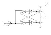
図10は、レベルシフター143の詳細構成例である。レベルシフター143は、インバーターIVD1とインバーターIVD2とP型トランジスターTPD1~TPD4とN型トランジスターTND1とN型トランジスターTND2とを含む。 FIG. 10 is a detailed configuration example of the
インバーターIVD1にはPWM信号DCS’が入力され、インバーターIVD2にはインバーターIVD1の出力信号が入力される。 A PWM signal DCS' is input to the inverter IVD1, and an output signal of the inverter IVD1 is input to the inverter IVD2.
P型トランジスターTPD1とP型トランジスターTPD3とN型トランジスターTND1は、電源ノードNVIとグランドノードNGNの間に直列接続される。P型トランジスターTPD2とP型トランジスターTPD4とN型トランジスターTND2は、電源ノードNVIとグランドノードNGNの間に直列接続される。P型トランジスターTPD1のゲートはP型トランジスターTPD2のドレインに接続され、P型トランジスターTPD2のゲートはP型トランジスターTPD1のドレインに接続される。P型トランジスターTPD2のドレイン電圧が、レベルシフター143の出力信号LSQとして出力される。P型トランジスターTPD3のゲートと、P型トランジスターTPD4のゲートには、不図示の電圧生成回路からバイアス電圧が入力される。N型トランジスターTND1のゲートには、インバーターIVD2の出力信号が入力され、N型トランジスターTND2のゲートには、インバーターIVD1の出力信号が入力される。 P-type transistor TPD1, P-type transistor TPD3, and N-type transistor TND1 are connected in series between power supply node NVI and ground node NGN. P-type transistor TPD2, P-type transistor TPD4 and N-type transistor TND2 are connected in series between power supply node NVI and ground node NGN. The gate of the P-type transistor TPD1 is connected to the drain of the P-type transistor TPD2, and the gate of the P-type transistor TPD2 is connected to the drain of the P-type transistor TPD1. The drain voltage of the P-type transistor TPD2 is output as the output signal LSQ of the
PWM信号DCS’がハイレベルのとき、P型トランジスターTPD2がオンであり且つN型トランジスターTND2がオフなので、ハイレベルの出力信号LSQが出力される。PWM信号DCS’がローレベルのとき、P型トランジスターTPD2がオフであり且つN型トランジスターTND2がオンなので、ローレベルの出力信号LSQが出力される。 When the PWM signal DCS' is at a high level, the P-type transistor TPD2 is on and the N-type transistor TND2 is off, so a high level output signal LSQ is output. When the PWM signal DCS' is at low level, the P-type transistor TPD2 is off and the N-type transistor TND2 is on, so the output signal LSQ at low level is output.
図11に、ドライバー回路141の詳細構成例を示す。ドライバー回路141は、インバーターIVE1、IVE2とノア回路NREとアンド回路ANEとバッファーBFEとP型トランジスターTPEとN型トランジスターTNEとを含む。 FIG. 11 shows a detailed configuration example of the
インバーターIVE2には、レベルシフター143の出力信号LSQが入力される。ノア回路NREには、インバーターIVE1の出力信号とバッファーBFEの出力信号が入力される。インバーターIVE2には、ノア回路NREの出力信号が入力される。アンド回路ANEには、インバーターIVE1の出力信号とインバーターIVE2の出力信号が入力される。バッファーBFEには、アンド回路ANEの出力信号が入力される。 The output signal LSQ of the
P型トランジスターTPEとN型トランジスターTNEは、ゲート用電源電圧VRHのノードとソース用電源電圧VRLのノードとの間に直列接続される。P型トランジスターTPEのゲートには、インバーターIVE2の出力信号が入力される。N型トランジスターTNEのゲートには、バッファーBFEの出力信号が入力される。P型トランジスターTPEのソース及びN型トランジスターTNEのソースから、駆動信号GTAが出力される。 The P-type transistor TPE and the N-type transistor TNE are connected in series between the node of the power supply voltage VRH for the gate and the node of the power supply voltage VRL for the source. An output signal of the inverter IVE2 is input to the gate of the P-type transistor TPE. An output signal of the buffer BFE is input to the gate of the N-type transistor TNE. A drive signal GTA is output from the source of the P-type transistor TPE and the source of the N-type transistor TNE.
レベルシフター143の出力信号LSQがローレベルのとき、インバーターIVE2の出力信号がハイレベルであり、バッファーBFEの出力信号がハイレベルなので、ローレベルの駆動信号GTAが出力される。レベルシフター143の出力信号LSQがハイレベルのとき、インバーターIVE2の出力信号がローレベルであり、バッファーBFEの出力信号がローレベルなので、ハイレベルの駆動信号GTAが出力される。 When the output signal LSQ of the
図12に、ポンピング用ドライバー回路142の詳細構成例を示す。ポンピング用ドライバー回路142は、インバーターIVF1、IVF2とノア回路NRFとアンド回路ANFとバッファーBFFとP型トランジスターTPFとN型トランジスターTNFとを含む。 FIG. 12 shows a detailed configuration example of the pumping
インバーターIVE2には、PWM信号DCS’が入力される。P型トランジスターTPFとN型トランジスターTNFは、電源電圧VDRのノードとグランドノードNGNとの間に直列接続される。P型トランジスターTPFのソース及びN型トランジスターTNFのソースから、ポンピング用駆動信号SPMPが出力される。構成要素間の接続関係と回路動作については、図11のドライバー回路141と同様である。 A PWM signal DCS' is input to the inverter IVE2. P-type transistor TPF and N-type transistor TNF are connected in series between a node of power supply voltage VDR and ground node NGN. A pumping drive signal SPMP is output from the source of the P-type transistor TPF and the source of the N-type transistor TNF. The connection relationship between components and the circuit operation are the same as those of the
なお、以上ではPWM信号DCS’のハイデューティーによってスイッチング素子11のオンデューティーが決定される例を説明したが、PWM信号DCS’のローデューティーによってスイッチング素子11のオンデューティーが決定されてもよい。例えば、図11のインバーターIVE1及び図12のインバーターIVF1が省略されてもよい。 In the above description, the on-duty of the switching
以上の第1詳細構成例、第3詳細構成例及び第4詳細構成例では、駆動回路110はドライバー回路141を含む。ドライバー回路141は、レベルシフター143の出力信号LSQをバッファリングして駆動信号GTAを出力する。 In the first detailed configuration example, the third detailed configuration example, and the fourth detailed configuration example, the
本実施形態によれば、ドライバー回路141がレベルシフター143の出力信号LSQをバッファリングすることで、レベルシフター143の駆動力よりも高い駆動力でスイッチング素子11のゲートを駆動できる。 According to the present embodiment, the
また第2~第4詳細構成例では、駆動回路110はポンピング用ドライバー回路142を含む。ポンピング用ドライバー回路142は、PWM信号DCS’をバッファリングしたポンピング用駆動信号SPMPをキャパシター18の他端に出力する。キャパシター18の一端は、スイッチング素子11であるトランジスターのゲートに接続される。 Further, in the second to fourth detailed configuration examples, the
本実施形態によれば、ポンピング用ドライバー回路142がキャパシター18を介してスイッチング素子11のゲートをポンピングできる。これにより、ポンピング用ドライバー回路142を設けずにレベルシフター143或いはドライバー回路141によりスイッチング素子11のゲートを駆動する場合に比べて、スイッチング素子11のゲート電圧波形が急峻に変化する。 According to this embodiment, the pumping
また本実施形態では、集積回路装置100は、第2レギュレーターであるレギュレーター132を含む。レギュレーター132は、グランド電圧GNDを基準に電源電圧VDRを生成する。電源電圧VDRは、ソース用電源電圧VRLより低い。ポンピング用ドライバー回路142は、電源電圧VDRとグランド電圧GNDとに基づいて、ポンピング用駆動信号SPMPをキャパシター18の他端に出力する。 Also, in this embodiment, the
本実施形態によれば、キャパシター18によりポンピング用駆動信号SPMPがACカップリングされるので、ポンピング用ドライバー回路142は、グランド電圧GNDを基準とした電源系により動作することが可能である。上述したように、駆動信号GTAの電圧は、比較的高い電圧であるため、例えばショート等による故障又は破壊を考慮すると、駆動信号GTAの駆動力は低い方が好ましい。この点、比較的低い電圧で動作するポンピング用ドライバー回路142を設けたことで、駆動信号GTAの駆動力を低くすることが可能である。 According to this embodiment, the pumping drive signal SPMP is AC-coupled by the
また本実施形態では、駆動回路110は抵抗145を含む。抵抗145は、スイッチング素子11であるトランジスターのソースとゲートの間に設けられる。 Also in this embodiment, the
本実施形態によれば、ACカップリングすることなくスイッチング素子11のゲートを駆動可能であるため、スイッチング素子11のソースとゲートの間に抵抗145が設けられていても、スイッチング素子11のゲートソース間電圧が低下していかない。これにより、図1で説明したような光源回路17の外付け部品群19を省略可能となる。 According to this embodiment, since the gate of the switching
また本実施形態では、駆動回路110はバッファーアンプ回路144を含む。バッファーアンプ回路144は、スイッチング素子11であるトランジスターのソース電圧をバッファリングしたソース用電源電圧VRLを、レギュレーター131に出力する。 Also, in this embodiment, the
ゲート用電源電圧VRHに関する消費電流はレギュレーター131からソース用電源電圧VRLのノードに流れる。本実施形態によれば、その電流をバッファーアンプ回路144が吸収するので、その電流が光源回路17のインダクター14に流れない。これにより、ゲート用電源電圧VRHに関する消費電流が発光制御に影響を与えない。 A current consumption related to the gate power supply voltage VRH flows from the
4.スイッチング素子としてP型トランジスターを用いた場合の詳細構成例
図13は、スイッチング素子11がP型トランジスターである場合における光源装置200の詳細構成例である。なお、図13において、図2に示した構成要素の一部を省略しているが、それらの構成要素については図2と同様である。以下、図2或いは図7と異なる部分について説明する。4. Detailed Configuration Example Using P-Type Transistor as Switching Element FIG. 13 is a detailed configuration example of the
光源回路10において、発光素子15のカソードが接続されるノードをノードNSとする。スイッチング素子11であるP型トランジスターのソースはノードNSに接続され、ドレインは第1ノードN1に接続される。 In the
集積回路装置100は、端子TVRLに代えて端子TVRHを含み、レギュレーター131に代えてレギュレーター133を含む。端子TVRHは、ノードNSにACカップリングされることなく接続されており、端子TVRHには、スイッチング素子11のソース電圧が入力される。バッファーアンプ回路144は、スイッチング素子11のソース電圧をバッファリングし、バッファリング後の電圧をソース用電源電圧VRH’としてレギュレーター133に出力する。レギュレーター133は、ソース用電源電圧VRH’と入力電源電圧VINを用いて、ソース用電源電圧VRH’より所定電圧だけ低いゲート用電源電圧VRL’を生成する。
レベルシフター143は、PWM信号DCS’を受けて、ハイレベルが電源電圧VDRであり且つローレベルがグランド電圧GNDである信号を生成し、その信号を、ハイレベルがソース用電源電圧VRH’であり且つローレベルがゲート用電源電圧VRL’である出力信号LSQにレベルシフトする。ドライバー回路141は、ゲート用電源電圧VRL’とソース用電源電圧VRH’を電源として動作する。ドライバー回路141は、出力信号LSQをバッファリングし、バッファリング後の駆動信号GTAを、端子TGTAを介してスイッチング素子11のゲートに出力する。 The
なお、第1詳細構成例、第2詳細構成例又は第4詳細構成例と同様に、ドライバー回路141が省略されてもよいし、又はポンピング用ドライバー回路142及びキャパシター18が省略されてもよいし、又はバッファーアンプ回路144が省略されてもよい。 As in the first detailed configuration example, the second detailed configuration example, or the fourth detailed configuration example, the
図14は、レギュレーター133の詳細構成例である。レギュレーター133は、電流源回路IBDとツェナーダイオードDIDと抵抗RD1と抵抗RD2とP型トランジスターNTDとを含む。 FIG. 14 is a detailed configuration example of the
電流源回路IBDは、ツェナーダイオードDIDのアノードとグランドノードとの間に設けられる。ツェナーダイオードDIDのカソードはソース用電源電圧VRH’のノードに接続される。電流源回路IBDがツェナーダイオードDIDのカソードからアノードに電流を流すことで、ツェナーダイオードDIDのアノードは、ソース用電源電圧VRH’からツェナー電圧だけ降下した電圧となる。 A current source circuit IBD is provided between the anode of the Zener diode DID and the ground node. The cathode of the Zener diode DID is connected to the node of the source power supply voltage VRH'. The current source circuit IBD causes a current to flow from the cathode to the anode of the Zener diode DID, so that the anode of the Zener diode DID becomes a voltage that is the Zener voltage dropped from the source power supply voltage VRH'.
抵抗RD1と抵抗RD2は、ツェナーダイオードDICのカソードとアノードの間に直列接続される。P型トランジスターNTDのドレインはグランドノードに接続され、ゲートは、抵抗RD1と抵抗RD2の間のノードに接続される。抵抗RD1と抵抗RD2が、ツェナーダイオードDIDのアノードの電圧と、ソース用電源電圧VRH’との間を分圧し、その分圧電圧がP型トランジスターNTDのゲートに入力される。これにより、P型トランジスターNTDのソース電圧は、分圧電圧からP型トランジスターNTDの閾値電圧だけ高い電圧となり、その電圧がゲート用電源電圧VRL’として出力される。分圧電圧が、ソース用電源電圧VRH’から所定電圧と閾値電圧を減算した電圧付近となるように、抵抗RD1と抵抗RD2の分圧比が設定される。これにより、ゲート用電源電圧VRL’は、ソース用電源電圧VRH’よりも所定電圧だけ低い電圧となる。 Resistor RD1 and resistor RD2 are connected in series between the cathode and anode of Zener diode DIC. The P-type transistor NTD has a drain connected to the ground node and a gate connected to a node between the resistors RD1 and RD2. The resistors RD1 and RD2 divide the voltage between the anode voltage of the Zener diode DID and the source power supply voltage VRH', and the divided voltage is input to the gate of the P-type transistor NTD. As a result, the source voltage of the P-type transistor NTD becomes a voltage higher than the divided voltage by the threshold voltage of the P-type transistor NTD, and this voltage is output as the gate power supply voltage VRL'. The voltage dividing ratio of the resistors RD1 and RD2 is set so that the divided voltage is close to the voltage obtained by subtracting the predetermined voltage and the threshold voltage from the source power supply voltage VRH'. As a result, the gate power supply voltage VRL' becomes a voltage lower than the source power supply voltage VRH' by a predetermined voltage.
以上に説明した本実施形態の集積回路装置は、スイッチング素子を制御する。スイッチング素子は、電源ノードとインダクターの一端との間において発光素子のカソード側に発光素子に直列に設けられる。集積回路装置は、駆動回路とレギュレーターとを含む。駆動回路は、スイッチング素子に駆動信号を出力し、駆動信号をアクティブにすることでスイッチング素子をオンさせ、駆動信号を非アクティブにすることでスイッチング素子をオフさせる。レギュレーターは、スイッチング素子であるトランジスターのソース電圧と同電位であるソース用電源電圧が入力され、ソース用電源電圧を基準とするゲート用電源電圧を生成する。駆動回路は、ゲート用電源電圧とソース用電源電圧に基づいてPWM信号をレベルシフトするレベルシフターを有し、レベルシフターの出力信号に基づく駆動信号をトランジスターのゲートに出力する。 The integrated circuit device of this embodiment described above controls the switching elements. The switching element is provided in series with the light emitting element on the cathode side of the light emitting element between the power supply node and one end of the inductor. An integrated circuit device includes a driver circuit and a regulator. The drive circuit outputs a drive signal to the switching element, turns on the switching element by activating the drive signal, and turns off the switching element by deactivating the drive signal. The regulator receives a source power supply voltage having the same potential as the source voltage of a transistor, which is a switching element, and generates a gate power supply voltage based on the source power supply voltage. The drive circuit has a level shifter that level-shifts the PWM signal based on the gate power supply voltage and the source power supply voltage, and outputs a drive signal based on the output signal of the level shifter to the gate of the transistor.
本実施形態によれば、スイッチング素子のゲートに入力される駆動信号のローレベルがソース用電源電圧となり、ハイレベルが、ソース用電源電圧を基準とするゲート用電源電圧となる。これにより、駆動信号をACカップリングせずにスイッチング素子のゲートに入力しても、スイッチング素子が適切にオン又はオフに制御される。即ち、スイッチング素子を適切にオン又はオフに制御するための外付け部品を設ける必要がなくなるため、外付け部品の削減と、スイッチング素子の適切な制御とが両立可能となる。 According to this embodiment, the low level of the drive signal input to the gate of the switching element is the source power supply voltage, and the high level is the gate power supply voltage based on the source power supply voltage. As a result, even if the drive signal is input to the gate of the switching element without AC coupling, the switching element is controlled to be turned on or off appropriately. That is, since it is not necessary to provide an external component for appropriately turning on or off the switching element, it is possible to achieve both a reduction in the number of external components and appropriate control of the switching element.
また本実施形態では、駆動回路はドライバー回路を含んでもよい。ドライバー回路は、レベルシフターの出力信号をバッファリングして駆動信号を出力してもよい。 Also in this embodiment, the drive circuit may include a driver circuit. The driver circuit may buffer the output signal of the level shifter and output the drive signal.
本実施形態によれば、ドライバー回路がレベルシフターの出力信号をバッファリングすることで、レベルシフターの駆動力よりも高い駆動力でスイッチング素子のゲートを駆動できる。 According to this embodiment, the driver circuit buffers the output signal of the level shifter, so that the gate of the switching element can be driven with higher driving power than that of the level shifter.
また本実施形態では、駆動回路はポンピング用ドライバー回路を含んでもよい。ポンピング用ドライバー回路は、PWM信号をバッファリングしたポンピング用駆動信号を、一端がトランジスターのゲートに接続されるキャパシターの他端に出力してもよい。 Also in this embodiment, the driving circuit may include a pumping driver circuit. The pumping driver circuit may output a pumping drive signal obtained by buffering the PWM signal to the other end of a capacitor having one end connected to the gate of the transistor.
本実施形態によれば、ポンピング用ドライバー回路がキャパシターを介してスイッチング素子のゲートをポンピングできる。これにより、ポンピング用ドライバー回路を設けずにレベルシフター或いはドライバー回路によりスイッチング素子のゲートを駆動する場合に比べて、スイッチング素子のゲート電圧波形が急峻に変化する。 According to this embodiment, the pumping driver circuit can pump the gate of the switching element through the capacitor. As a result, the gate voltage waveform of the switching element changes sharply compared to the case where the gate of the switching element is driven by a level shifter or a driver circuit without providing a pumping driver circuit.
また本実施形態では、レギュレーターを第1レギュレーターとしたとき、集積回路装置は第2レギュレーターを含んでもよい。第2レギュレーターは、グランド電圧を基準に、ソース用電源電圧より低い電源電圧を生成してもよい。ポンピング用ドライバー回路は、電源電圧とグランド電圧とに基づいて、ポンピング用駆動信号をキャパシターの他端に出力してもよい。 Further, in this embodiment, when the regulator is the first regulator, the integrated circuit device may include the second regulator. The second regulator may generate a power supply voltage lower than the source power supply voltage with reference to the ground voltage. The pumping driver circuit may output a pumping drive signal to the other end of the capacitor based on the power supply voltage and the ground voltage.
本実施形態によれば、キャパシターによりポンピング用駆動信号がACカップリングされるので、ポンピング用ドライバー回路は、グランド電圧を基準とした電源系により動作することが可能である。駆動信号の電圧は、比較的高い電圧であるため、例えばショート等による故障又は破壊を考慮すると、駆動信号の駆動力は低い方が好ましい。この点、比較的低い電圧で動作するポンピング用ドライバーを設けたことで、駆動信号の駆動力を低くすることが可能である。 According to this embodiment, since the pumping drive signal is AC-coupled by the capacitor, the pumping driver circuit can be operated by a power supply system based on the ground voltage. Since the voltage of the drive signal is a relatively high voltage, it is preferable that the driving power of the drive signal is low in consideration of failure or destruction due to, for example, a short circuit. In this respect, the provision of the pumping driver that operates at a relatively low voltage makes it possible to reduce the driving power of the drive signal.
また本実施形態では、駆動回路は、トランジスターのソースとゲートの間に設けられる抵抗を含んでもよい。 In this embodiment, the drive circuit may also include a resistor provided between the source and gate of the transistor.
本実施形態によれば、ACカップリングすることなくスイッチング素子のゲートを駆動可能であるため、スイッチング素子のソースとゲートの間に抵抗が設けられていても、スイッチング素子のゲートソース間電圧が低下していかない。これにより、光源回路の外付け部品の削減と、スイッチング素子の適切な制御とが、両立可能になる。 According to this embodiment, since the gate of the switching element can be driven without AC coupling, even if a resistor is provided between the source and the gate of the switching element, the gate-source voltage of the switching element decreases. I can't do it. This makes it possible to achieve both a reduction in external components of the light source circuit and appropriate control of the switching elements.
また本実施形態では、駆動回路はバッファーアンプ回路を含んでもよい。バッファーアンプ回路は、ソース電圧をバッファリングしたソース用電源電圧をレギュレーターに出力してもよい。 Further, in this embodiment, the drive circuit may include a buffer amplifier circuit. The buffer amplifier circuit may output a source power supply voltage obtained by buffering the source voltage to the regulator.
ゲート用電源電圧に関する消費電流はレギュレーターからソース用電源電圧のノードに流れる。本実施形態によれば、その電流をバッファーアンプ回路が吸収するので、その電流が光源回路のインダクターに流れない。これにより、ゲート用電源電圧に関する消費電流が発光制御に影響を与えない。 The consumption current for the gate power supply voltage flows from the regulator to the source power supply voltage node. According to this embodiment, the current is absorbed by the buffer amplifier circuit, so the current does not flow through the inductor of the light source circuit. As a result, current consumption related to the gate power supply voltage does not affect light emission control.
また本実施形態では、集積回路装置はアナログ調光駆動回路を含んでもよい。アナログ調光駆動回路は、アナログ調光スイッチング素子にアナログ調光駆動信号を出力してもよい。アナログ調光スイッチング素子は、インダクターの他端からグランドノードに流れる電流を制御する。アナログ調光駆動回路は、駆動信号がアクティブである期間において、アナログ調光駆動信号をアクティブにすることでアナログ調光スイッチング素子をオンさせ、アナログ調光駆動信号を非アクティブにすることでアナログ調光スイッチング素子をオフさせてもよい。 Also in this embodiment, the integrated circuit device may include an analog dimming driver circuit. The analog dimming drive circuit may output an analog dimming drive signal to the analog dimming switching element. An analog dimming switching element controls the current flowing from the other end of the inductor to the ground node. The analog dimming drive circuit turns on the analog dimming switching element by activating the analog dimming drive signal while the drive signal is active, and turns on the analog dimming switching element by deactivating the analog dimming drive signal. The optical switching element may be turned off.
本実施形態によれば、アナログ調光駆動回路のスイッチングレギュレート制御により調光するアナログ調光モードと、駆動回路のPWM駆動により調光するPWM調光モードと、を実現できる。アナログ調光モードにおいて、或いはPWM調光モードにおける比較的オンデューティーが長い場合において、スイッチング素子が長時間オンになるが、本実施形態によれば、スイッチング素子のゲートソース間電圧が低下しないので、光源回路の外付け部品の削減と、スイッチング素子の適切な制御とが、両立可能になる。 According to this embodiment, an analog dimming mode for dimming by switching regulation control of the analog dimming drive circuit and a PWM dimming mode for dimming by PWM driving of the drive circuit can be realized. In the analog dimming mode or when the on-duty is relatively long in the PWM dimming mode, the switching element is turned on for a long time. It is possible to achieve both a reduction in the number of external components of the light source circuit and appropriate control of the switching elements.
また本実施形態の光源装置は、上記のいずれか一項に記載の集積回路装置と、発光素子と、スイッチング素子と、インダクターと、を含む。 Further, a light source device of this embodiment includes the integrated circuit device according to any one of the above items, a light emitting element, a switching element, and an inductor.
なお、上記のように本実施形態について詳細に説明したが、本開示の新規事項及び効果から実体的に逸脱しない多くの変形が可能であることは当業者には容易に理解できるであろう。従って、このような変形例はすべて本開示の範囲に含まれるものとする。例えば、明細書又は図面において、少なくとも一度、より広義又は同義な異なる用語と共に記載された用語は、明細書又は図面のいかなる箇所においても、その異なる用語に置き換えることができる。また本実施形態及び変形例の全ての組み合わせも、本開示の範囲に含まれる。また集積回路装置、光源回路及び光源装置等の構成及び動作等も、本実施形態で説明したものに限定されず、種々の変形実施が可能である。 Although the present embodiment has been described in detail as above, it will be easily understood by those skilled in the art that many modifications are possible without substantially departing from the novel matters and effects of the present disclosure. Accordingly, all such modifications are intended to be included within the scope of this disclosure. For example, a term described at least once in the specification or drawings together with a different, broader or synonymous term can be replaced with the different term anywhere in the specification or drawings. All combinations of this embodiment and modifications are also included in the scope of the present disclosure. Also, the configurations and operations of the integrated circuit device, the light source circuit, the light source device, etc. are not limited to those described in the present embodiment, and various modifications are possible.
10…光源回路、11…スイッチング素子、12…アナログ調光スイッチング素子、14…インダクター、15…発光素子、17…光源回路、18…キャパシター、19…外付け部品群、100…集積回路装置、110…駆動回路、112…アナログ調光駆動回路、114…制御回路、120…アナログ調光制御回路、131,132…レギュレーター、141…ドライバー回路、142…ポンピング用ドライバー回路、143…レベルシフター、144…バッファーアンプ回路、145…抵抗、146…ツェナーダイオード、200…光源装置、DCS,DCS'…PWM信号、GTA…駆動信号、GTB…アナログ調光駆動信号、NGN…グランドノード、NVI…電源ノード、VDR…電源電圧、VIN…入力電源電圧、VRH…ゲート用電源電圧、VRL…ソース用電源電圧DESCRIPTION OF
Claims (8)
Translated fromJapanese前記スイッチング素子に駆動信号を出力し、前記駆動信号をアクティブにすることで前記スイッチング素子をオンさせ、前記駆動信号を非アクティブにすることで前記スイッチング素子をオフさせる駆動回路と、
前記スイッチング素子であるトランジスターのソース電圧と同電位であるソース用電源電圧が入力され、前記ソース用電源電圧を基準とするゲート用電源電圧を生成するレギュレーターと、
を含み、
前記駆動回路は、
前記ゲート用電源電圧と前記ソース用電源電圧に基づいてPWM信号をレベルシフトするレベルシフターを有し、前記レベルシフターの出力信号に基づく前記駆動信号を前記トランジスターのゲートに出力することを特徴とする集積回路装置。An integrated circuit device for controlling a switching element provided in series with a light emitting element on the cathode side of the light emitting element between a power supply node and one end of an inductor,
a drive circuit that outputs a drive signal to the switching element, turns on the switching element by activating the drive signal, and turns off the switching element by deactivating the drive signal;
a regulator that receives a source power supply voltage having the same potential as the source voltage of the transistor that is the switching element and generates a gate power supply voltage based on the source power supply voltage;
including
The drive circuit is
A level shifter for level-shifting a PWM signal based on the gate power supply voltage and the source power supply voltage is provided, and the drive signal based on the output signal of the level shifter is output to the gate of the transistor. Integrated circuit device.
前記駆動回路は、
前記レベルシフターの前記出力信号をバッファリングして前記駆動信号を出力するドライバー回路を含むことを特徴とする集積回路装置。The integrated circuit device of claim 1, wherein
The drive circuit is
An integrated circuit device comprising a driver circuit that buffers the output signal of the level shifter and outputs the drive signal.
前記駆動回路は、
前記PWM信号をバッファリングしたポンピング用駆動信号を、一端が前記トランジスターの前記ゲートに接続されるキャパシターの他端に出力するポンピング用ドライバー回路を含むことを特徴とする集積回路装置。The integrated circuit device according to claim 1 or 2,
The drive circuit is
An integrated circuit device comprising a pumping driver circuit for outputting a pumping drive signal obtained by buffering the PWM signal to the other end of a capacitor having one end connected to the gate of the transistor.
前記レギュレーターを第1レギュレーターとしたとき、グランド電圧を基準に、前記ソース用電源電圧より低い電源電圧を生成する第2レギュレーターを含み、
前記ポンピング用ドライバー回路は、
前記電源電圧と前記グランド電圧とに基づいて、前記ポンピング用駆動信号を前記キャパシターの前記他端に出力することを特徴とする集積回路装置。The integrated circuit device according to claim 3,
including a second regulator that generates a power supply voltage lower than the source power supply voltage with reference to a ground voltage when the regulator is the first regulator;
The pumping driver circuit includes:
An integrated circuit device, wherein the pumping drive signal is output to the other end of the capacitor based on the power supply voltage and the ground voltage.
前記駆動回路は、
前記トランジスターのソースと前記ゲートの間に設けられる抵抗を含むことを特徴とする集積回路装置。The integrated circuit device according to any one of claims 1 to 4,
The drive circuit is
An integrated circuit device comprising a resistor provided between the source of the transistor and the gate.
前記駆動回路は、
前記ソース電圧をバッファリングした前記ソース用電源電圧を前記レギュレーターに出力するバッファーアンプ回路を含むことを特徴とする集積回路装置。The integrated circuit device according to any one of claims 1 to 5,
The drive circuit is
An integrated circuit device comprising a buffer amplifier circuit for outputting the source power supply voltage obtained by buffering the source voltage to the regulator.
前記インダクターの他端からグランドノードに流れる電流を制御するアナログ調光スイッチング素子にアナログ調光駆動信号を出力し、前記駆動信号がアクティブである期間において、前記アナログ調光駆動信号をアクティブにすることで前記アナログ調光スイッチング素子をオンさせ、前記アナログ調光駆動信号を非アクティブにすることで前記アナログ調光スイッチング素子をオフさせるアナログ調光駆動回路を含むことを特徴とする集積回路装置。The integrated circuit device according to any one of claims 1 to 6,
Outputting an analog dimming drive signal to an analog dimming switching element that controls current flowing from the other end of the inductor to a ground node, and activating the analog dimming drive signal during a period in which the drive signal is active. and an analog dimming drive circuit for turning on the analog dimming switching element and turning off the analog dimming switching element by deactivating the analog dimming drive signal.
前記発光素子と、
前記スイッチング素子と、
前記インダクターと、
を含むことを特徴とする光源装置。an integrated circuit device according to any one of claims 1 to 7;
the light emitting element;
the switching element;
the inductor;
A light source device comprising:
Priority Applications (3)
| Application Number | Priority Date | Filing Date | Title |
|---|---|---|---|
| JP2021009263AJP2022113203A (en) | 2021-01-25 | 2021-01-25 | Integrated circuit device and light source device |
| CN202210079965.9ACN114793376B (en) | 2021-01-25 | 2022-01-24 | Integrated circuit device and light source device |
| US17/582,362US11632831B2 (en) | 2021-01-25 | 2022-01-24 | Integrated circuit device and light source device |
Applications Claiming Priority (1)
| Application Number | Priority Date | Filing Date | Title |
|---|---|---|---|
| JP2021009263AJP2022113203A (en) | 2021-01-25 | 2021-01-25 | Integrated circuit device and light source device |
Publications (1)
| Publication Number | Publication Date |
|---|---|
| JP2022113203Atrue JP2022113203A (en) | 2022-08-04 |
Family
ID=82460596
Family Applications (1)
| Application Number | Title | Priority Date | Filing Date |
|---|---|---|---|
| JP2021009263APendingJP2022113203A (en) | 2021-01-25 | 2021-01-25 | Integrated circuit device and light source device |
Country Status (3)
| Country | Link |
|---|---|
| US (1) | US11632831B2 (en) |
| JP (1) | JP2022113203A (en) |
| CN (1) | CN114793376B (en) |
Families Citing this family (1)
| Publication number | Priority date | Publication date | Assignee | Title |
|---|---|---|---|---|
| CN113394954A (en)* | 2020-03-12 | 2021-09-14 | 深圳光峰科技股份有限公司 | Driving circuit, power circuit and projection equipment |
Family Cites Families (10)
| Publication number | Priority date | Publication date | Assignee | Title |
|---|---|---|---|---|
| JP2009077208A (en)* | 2007-09-21 | 2009-04-09 | Sony Corp | Interface circuit having voltage-level shifting function, semiconductor integrated circuit, and display device |
| JP5416008B2 (en)* | 2010-03-24 | 2014-02-12 | ルネサスエレクトロニクス株式会社 | Level shift circuit, data driver, and display device |
| US20110273430A1 (en)* | 2010-05-05 | 2011-11-10 | Intersil Americas Inc. | Voltage level shifting with reduced power consumption |
| JP6841099B2 (en) | 2017-03-15 | 2021-03-10 | セイコーエプソン株式会社 | Semiconductor devices, light emission control circuits, and electronic devices |
| CN109640433B (en)* | 2017-10-05 | 2023-03-31 | 精工爱普生株式会社 | Light emission control circuit, light source device, and projection type image display device |
| JP2019071269A (en) | 2017-10-05 | 2019-05-09 | セイコーエプソン株式会社 | Light emission control circuit, light source device, and projection type video display device |
| JP6988515B2 (en) | 2018-01-25 | 2022-01-05 | セイコーエプソン株式会社 | Light source device, projection type display device, and semiconductor device |
| US10362645B1 (en)* | 2018-04-18 | 2019-07-23 | Linear Technology Holding, LLC | Negative charge pump doubling output voltage range for step-up LED driver |
| CA3110739C (en)* | 2018-08-31 | 2024-05-14 | Lutron Technology Company Llc | Drive circuit for a light-emitting diode light source |
| JP2020136079A (en)* | 2019-02-20 | 2020-08-31 | セイコーエプソン株式会社 | Light-emitting control device, light source device and projection type video display device |
- 2021
- 2021-01-25JPJP2021009263Apatent/JP2022113203A/enactivePending
- 2022
- 2022-01-24USUS17/582,362patent/US11632831B2/enactiveActive
- 2022-01-24CNCN202210079965.9Apatent/CN114793376B/enactiveActive
Also Published As
| Publication number | Publication date |
|---|---|
| US11632831B2 (en) | 2023-04-18 |
| CN114793376B (en) | 2025-02-18 |
| CN114793376A (en) | 2022-07-26 |
| US20220240357A1 (en) | 2022-07-28 |
Similar Documents
| Publication | Publication Date | Title |
|---|---|---|
| US8159140B2 (en) | Load driving apparatus | |
| US7535189B2 (en) | Motor drive circuit | |
| US20150207399A1 (en) | Pwm controller capable of controlling output current ripple via a resistor, and led driver circuit using same | |
| US10506677B2 (en) | Light source device, projection type display device, and semiconductor device | |
| US8884545B2 (en) | LED driving system and driving method thereof | |
| JP2007028783A (en) | STEP-UP SWITCHING REGULATOR, ITS CONTROL CIRCUIT, AND ELECTRONIC DEVICE USING THE SAME | |
| JP2011034547A (en) | Constant current device and led device using the same | |
| JP2018152318A (en) | Semiconductor device, light emission control circuit, and electronic device | |
| US20110032244A1 (en) | Light-emitting element drive device and light-emitting device | |
| US8686783B2 (en) | Level shifter and boost driving circuit | |
| US7986108B2 (en) | LED driver and start-up feedback circuit therein | |
| CN114793376B (en) | Integrated circuit device and light source device | |
| JP2016208082A (en) | Current driver circuit | |
| US11522535B2 (en) | Semiconductor device | |
| CN111629483A (en) | Light emission control device, light source device, and projection type image display device | |
| CN111712015B (en) | Light emission control device, light source device, and projection type image display device | |
| US11032880B2 (en) | Light emission control device, light source device, and projection-type video display apparatus | |
| JP2012009651A (en) | Current driving device | |
| US20210298148A1 (en) | Dc-dc power supply and light emitting device | |
| JP2011258797A (en) | Drive control circuit of light-emitting diode and backlight system | |
| JP2019129080A (en) | Light source device, projection type display device, and semiconductor device | |
| TWI839303B (en) | Switching dc-dc converter | |
| JP2022128728A (en) | Integrated circuit device and light source device | |
| JP5149458B1 (en) | LED lighting device | |
| KR100658067B1 (en) | Power supply circuit of liquid crystal display |