Movatterモバイル変換


[0]ホーム

URL:


JP2022108487A - wiring board - Google Patents

wiring board
Download PDF

Info

Publication number
JP2022108487A
JP2022108487AJP2021003507AJP2021003507AJP2022108487AJP 2022108487 AJP2022108487 AJP 2022108487AJP 2021003507 AJP2021003507 AJP 2021003507AJP 2021003507 AJP2021003507 AJP 2021003507AJP 2022108487 AJP2022108487 AJP 2022108487A
Authority
JP
Japan
Prior art keywords
conductor
layer
insulating layer
pad
wiring board
Prior art date
Legal status (The legal status is an assumption and is not a legal conclusion. Google has not performed a legal analysis and makes no representation as to the accuracy of the status listed.)
Granted
Application number
JP2021003507A
Other languages
Japanese (ja)
Other versions
JP7587428B2 (en
Inventor
俊輔 酒井
Shunsuke Sakai
Current Assignee (The listed assignees may be inaccurate. Google has not performed a legal analysis and makes no representation or warranty as to the accuracy of the list.)
Ibiden Co Ltd
Original Assignee
Ibiden Co Ltd
Priority date (The priority date is an assumption and is not a legal conclusion. Google has not performed a legal analysis and makes no representation as to the accuracy of the date listed.)
Filing date
Publication date
Application filed by Ibiden Co LtdfiledCriticalIbiden Co Ltd
Priority to JP2021003507ApriorityCriticalpatent/JP7587428B2/en
Publication of JP2022108487ApublicationCriticalpatent/JP2022108487A/en
Application grantedgrantedCritical
Publication of JP7587428B2publicationCriticalpatent/JP7587428B2/en
Activelegal-statusCriticalCurrent
Anticipated expirationlegal-statusCritical

Links

Images

Landscapes

Abstract

Translated fromJapanese

【課題】配線基板の品質向上。【解決手段】実施形態の配線基板1は、第1絶縁層2と、第1絶縁層2の表面2a上に形成されている導体層3と、第1絶縁層2の表面2a上及び導体層3上に形成されていて、導体層3の少なくとも一部を露出させる開口4aを有するソルダーレジスト層4と、を含んでいて、第1面及びその反対面である第2面12を有している。導体層3は開口4aによって露出される導体パッド3aを含み、導体パッド3aにおける第1絶縁層2と反対側を向く表面3a1及び導体パッド3aの側面3a2全体がソルダーレジスト層4に覆われずに露出しており、導体パッド3aの縁部が第1絶縁層2の表面2aから離間している。【選択図】図3[Problem] Improving the quality of wiring boards. [Solution] A wiring board 1 according to an embodiment includes a first insulating layer 2, a conductor layer 3 formed on a surface 2a of the first insulating layer 2, and a solder resist layer 4 formed on the surface 2a of the first insulating layer 2 and on the conductor layer 3, and having an opening 4a that exposes at least a part of the conductor layer 3, and has a first surface and a second surface 12 that is the opposite surface. The conductor layer 3 includes a conductor pad 3a exposed by the opening 4a, and a surface 3a1 of the conductor pad 3a facing away from the first insulating layer 2 and a side surface 3a2 of the conductor pad 3a are exposed without being covered by the solder resist layer 4, and an edge of the conductor pad 3a is spaced from the surface 2a of the first insulating layer 2. [Selected Figure] Figure 3

Description

Translated fromJapanese

本発明は配線基板に関する。 The present invention relates to wiring boards.

特許文献1には、絶縁層上に形成されていて半導体素子に接合されるパッド部を有する多層配線基板が開示されている。絶縁層上にはソルダーレジストが設けられており、パッド部は、ソルダーレジストの開口中にソルダーレジストから離れた状態となるように配置されている。 Japanese Laid-Open Patent Publication No. 2004-100000 discloses a multilayer wiring board having a pad portion formed on an insulating layer and bonded to a semiconductor element. A solder resist is provided on the insulating layer, and the pads are arranged in the openings of the solder resist so as to be separated from the solder resist.

特開2004-22713号公報Japanese Patent Application Laid-Open No. 2004-22713

特許文献1の開示のように形成されたパッド部及びその下地の絶縁層には、銅などの金属からなるパッド部と主に樹脂からなる絶縁層との熱膨張率の相違や、パッド部に接続される外部の部品から加わる外力などによって応力が生じることがある。特に特許文献1の開示のようにソルダーレジストから離れた状態で配置されるパッド部では、金属と樹脂との熱膨張率の相違による応力がパッド部と絶縁層との界面やパッド部の端部付近の絶縁層に集中し易いと考えられる。応力の集中箇所においてクラックや界面剥離などの不具合が生じることがある。 In the pad formed as disclosed inPatent Document 1 and the underlying insulating layer, there is a difference in coefficient of thermal expansion between the pad made of metal such as copper and the insulating layer made mainly of resin, and Stress may be generated by an external force applied from an external component to be connected. In particular, as disclosed inPatent Document 1, in a pad portion arranged away from the solder resist, stress due to the difference in thermal expansion coefficient between the metal and the resin is applied to the interface between the pad portion and the insulating layer and the edge of the pad portion. It is considered that it tends to be concentrated in the nearby insulating layer. Problems such as cracks and interfacial peeling may occur at places where stress is concentrated.

本発明の配線基板は、第1絶縁層と、前記第1絶縁層の表面上に形成されている導体層と、前記第1絶縁層の前記表面上及び前記導体層上に形成されていて、前記導体層の少なくとも一部を露出させる開口を有するソルダーレジスト層と、を含んでいて、第1面及び前記第1面の反対面である第2面を有している。そして、前記導体層は前記開口によって露出される導体パッドを含み、前記導体パッドにおける前記第1絶縁層と反対側を向く表面及び前記導体パッドの側面全体が前記ソルダーレジスト層に覆われずに露出しており、前記導体パッドの縁部が前記第1絶縁層の前記表面から離間している。 The wiring board of the present invention comprises a first insulating layer, a conductor layer formed on the surface of the first insulating layer, and formed on the surface of the first insulating layer and the conductor layer, and a solder resist layer having an opening exposing at least a portion of the conductor layer, the solder resist layer having a first surface and a second surface opposite to the first surface. The conductor layer includes a conductor pad exposed through the opening, and the surface of the conductor pad facing away from the first insulating layer and the entire side surface of the conductor pad are exposed without being covered with the solder resist layer. and an edge of the contact pad is spaced from the surface of the first insulating layer.

本発明の実施形態によれば、配線基板に設けられる導体パッドにおいて必要な大きさの露出部分を確保しながらその周辺部における不具合の発生を抑制できることがある。 According to the embodiments of the present invention, it may be possible to suppress the occurrence of problems in the peripheral portion of the conductor pads provided on the wiring board while ensuring the necessary size of the exposed portion.

本発明の一実施形態の配線基板の一例を示す断面図。1 is a cross-sectional view showing an example of a wiring board according to one embodiment of the present invention; FIG.本発明の一実施形態の配線基板の一例を示す平面図。1 is a plan view showing an example of a wiring board according to one embodiment of the present invention; FIG.図1のIII部の拡大図。The enlarged view of the III section of FIG.図3のIV部の拡大図。The enlarged view of the IV section of FIG.本発明の一実施形態における導体パッドの縁部の他の例を示す断面図。FIG. 5 is a cross-sectional view showing another example of the edge of the conductor pad in one embodiment of the present invention;本発明の一実施形態における導体パッドの縁部の他の例を示す断面図。FIG. 5 is a cross-sectional view showing another example of the edge of the conductor pad in one embodiment of the present invention;本発明の一実施形態の配線基板の製造工程中の状態の一例を示す断面図。FIG. 4 is a cross-sectional view showing an example of a state during a manufacturing process of a wiring board according to one embodiment of the present invention;本発明の一実施形態の配線基板の製造工程中の状態の一例を示す断面図。FIG. 4 is a cross-sectional view showing an example of a state during a manufacturing process of a wiring board according to one embodiment of the present invention;本発明の一実施形態の配線基板の製造工程中の状態の一例を示す断面図。FIG. 4 is a cross-sectional view showing an example of a state during a manufacturing process of a wiring board according to one embodiment of the present invention;本発明の一実施形態の配線基板の製造工程中の状態の一例を示す断面図。FIG. 4 is a cross-sectional view showing an example of a state during a manufacturing process of a wiring board according to one embodiment of the present invention;本発明の一実施形態の配線基板の製造工程中の状態の一例を示す断面図。FIG. 4 is a cross-sectional view showing an example of a state during a manufacturing process of a wiring board according to one embodiment of the present invention;本発明の一実施形態の配線基板の製造工程中の状態の一例を示す断面図。FIG. 4 is a cross-sectional view showing an example of a state during a manufacturing process of a wiring board according to one embodiment of the present invention;

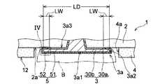
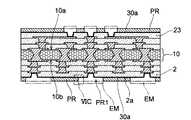
本発明の実施形態の配線基板が図面を参照しながら説明される。図1には、一実施形態の配線基板の一例である配線基板1の断面図が示されており、図2には、図1における下面側からの配線基板1の平面図が示されている。図2のI-I線での断面図が図1である。また図3には、図1のIII部の拡大図が示されている。 A wiring board according to an embodiment of the present invention will be described with reference to the drawings. FIG. 1 shows a cross-sectional view of awiring board 1 that is an example of a wiring board according to one embodiment, and FIG. 2 shows a plan view of thewiring board 1 from the lower surface side in FIG. . FIG. 1 is a cross-sectional view taken along line II of FIG. Also, FIG. 3 shows an enlarged view of part III of FIG.

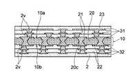
図1に示されるように、配線基板1は、絶縁層20と、絶縁層20の両面それぞれに交互に積層された導体層及び絶縁層とを含んでいる。絶縁層20の上面20a上には、3つの導体層31のそれぞれと2つの絶縁層21のそれぞれとが交互に積層され、その上に、さらに絶縁層23が積層されている。そして絶縁層23上に導体層(第2導体層)33が形成されている。絶縁層20の上面20aの反対面である下面20b上には、3つの導体層32のそれぞれと2つの絶縁層22のそれぞれとが交互に積層され、その上に、さらに絶縁層(第1絶縁層)2が積層されている。そして絶縁層2の表面2a上に導体層(第1導体層)3が形成されている。絶縁層23及び導体層33上には、ソルダーレジスト層40(第2ソルダーレジスト層)が形成されている。絶縁層2及び導体層3上にはソルダーレジスト層4(第1ソルダーレジスト層)が形成されている。実施形態の配線基板1は、絶縁層2と、絶縁層2の表面2a上に形成されている導体層3と、絶縁層2の表面2a上及び導体層3上に形成されているソルダーレジスト層4と、を少なくとも含んでいる。 As shown in FIG. 1 , thewiring board 1 includes aninsulating layer 20 and conductor layers and insulating layers alternately laminated on both sides of theinsulating layer 20 . Threeconductor layers 31 and twoinsulating layers 21 are alternately laminated on theupper surface 20a of theinsulating layer 20, and aninsulating layer 23 is further laminated thereon. A conductor layer (second conductor layer) 33 is formed on theinsulating layer 23 . On thelower surface 20b opposite to theupper surface 20a of theinsulating layer 20, each of the threeconductor layers 32 and each of the twoinsulating layers 22 are alternately laminated. layer) 2 are laminated. A conductor layer (first conductor layer) 3 is formed on thesurface 2 a of theinsulating layer 2 . A solder resist layer 40 (second solder resist layer) is formed on theinsulating layer 23 and theconductor layer 33 . A solder resist layer 4 (first solder resist layer) is formed on theinsulating layer 2 and theconductor layer 3 . Thewiring board 1 of the embodiment includes aninsulating layer 2, aconductor layer 3 formed on thesurface 2a of theinsulating layer 2, and a solder resist layer formed on thesurface 2a of theinsulating layer 2 and theconductor layer 3. 4 and at least.

配線基板1は、配線基板1の厚さ方向と直交する方向に広がる2つの表面として第1面11、及び第1面11の反対面である第2面12を有している。配線基板1の厚さ方向は、以下では単に「Z方向」とも称される。配線基板1において、絶縁層23、導体層33、及びソルダーレジスト層40は配線基板1の第1面11側に形成されており、配線基板1の第1面11側の表層部を形成している。第1面11は、絶縁層23、導体層33、及びソルダーレジスト層40それぞれにおけるZ方向に直交する露出面によって構成されている。また、絶縁層2、導体層3、及びソルダーレジスト層4は、配線基板1の第2面12側に形成されており、配線基板1の第2面12側の表層部を形成している。第2面12は、絶縁層2、導体層3、及びソルダーレジスト層4それぞれにおけるZ方向に直交する露出面によって構成されている。 Thewiring board 1 has afirst surface 11 and asecond surface 12 opposite to thefirst surface 11 as two surfaces extending in a direction perpendicular to the thickness direction of thewiring substrate 1 . The thickness direction of thewiring board 1 is hereinafter simply referred to as the "Z direction". In thewiring board 1 , theinsulating layer 23 , theconductor layer 33 , and thesolder resist layer 40 are formed on thefirst surface 11 side of thewiring board 1 and form the surface layer portion on thefirst surface 11 side of thewiring board 1 . there is Thefirst surface 11 is composed of exposed surfaces of theinsulating layer 23, theconductor layer 33, and thesolder resist layer 40, which are perpendicular to the Z direction. Theinsulating layer 2 , theconductor layer 3 , and thesolder resist layer 4 are formed on thesecond surface 12 side of thewiring board 1 and form a surface layer portion on thesecond surface 12 side of thewiring board 1 . Thesecond surface 12 is composed of exposed surfaces of theinsulating layer 2, theconductor layer 3, and thesolder resist layer 4, which are perpendicular to the Z direction.

絶縁層20には、導体層31と導体層32とを接続するスルーホール導体20cが形成されている。絶縁層20、その上面20a上の導体層31及び下面20b上の導体層32は、配線基板1のコア基板を構成している。絶縁層2及び絶縁層21~23それぞれには、絶縁層2及び絶縁層21~23それぞれを挟む導体層同士を接続するビア導体2vが形成されている。 Through-hole conductors 20 c are formed in theinsulating layer 20 to connect theconductor layers 31 and 32 . Theinsulating layer 20 , theconductor layer 31 on itsupper surface 20 a and theconductor layer 32 on itslower surface 20 b constitute a core substrate of thewiring board 1 . Viaconductors 2v are formed in each of theinsulating layer 2 and theinsulating layers 21 to 23 to connect the conductor layers sandwiching theinsulating layer 2 and theinsulating layers 21 to 23, respectively.

絶縁層2及び絶縁層20~23は、それぞれ、例えばエポキシ樹脂、ビスマレイミドトリアジン樹脂(BT樹脂)又はフェノール樹脂などの絶縁性樹脂を用いて形成される。各絶縁層は、ガラス繊維などの補強材(芯材)及び/又はシリカなどの無機フィラーを含んでいてもよい。 Theinsulating layer 2 and theinsulating layers 20 to 23 are each formed using an insulating resin such as epoxy resin, bismaleimide triazine resin (BT resin), or phenol resin. Each insulating layer may contain a reinforcing material (core material) such as glass fiber and/or an inorganic filler such as silica.

ソルダーレジスト層4、40は、例えばエポキシ樹脂又はポリイミド樹脂などの任意の絶縁性樹脂を用いて形成されている。ソルダーレジスト層40は、導体層33の一部又は全部を露出させる開口40aを有している。図1の例では、開口40aは、導体層33を部分的に露出させている。一方ソルダーレジスト層4は、導体層3の少なくとも一部を露出させる開口4aを有している。図1及び図2の例では、開口4aは、導体層3の全部を露出させている。 Thesolder resist layers 4 and 40 are formed using any insulating resin such as epoxy resin or polyimide resin. Thesolder resist layer 40 hasopenings 40 a that expose part or all of theconductor layer 33 . In the example of FIG. 1, the opening 40a partially exposes theconductor layer 33. As shown in FIG. On the other hand, thesolder resist layer 4 hasopenings 4 a that expose at least a portion of theconductor layer 3 . In the example of FIGS. 1 and 2, the opening 4a exposes theconductor layer 3 entirely.

導体層3及び導体層31~33、ビア導体2v、及びスルーホール導体20cは、銅又はニッケルなどの任意の金属を用いて形成され、例えば、銅箔などの金属箔、及び/又は、めっき若しくはスパッタリングなどで形成される金属膜によって構成される。従って導体層3及び導体層31~33、ビア導体2v、及びスルーホール導体20cは、2つ以上の金属層を有する多層構造を有し得る。しかし、導体層3及び導体層31~33、ビア導体2v、及びスルーホール導体20cは、単一の金属層だけを含む単層構造を有していてもよい。 Theconductor layer 3 and theconductor layers 31 to 33, thevia conductors 2v, and the through-hole conductors 20c are formed using any metal such as copper or nickel. It is composed of a metal film formed by sputtering or the like. Therefore, theconductor layer 3, theconductor layers 31 to 33, thevia conductors 2v, and the through-hole conductors 20c can have a multi-layer structure having two or more metal layers. However, theconductor layer 3, theconductor layers 31 to 33, thevia conductor 2v, and the through-hole conductor 20c may have a single layer structure including only a single metal layer.

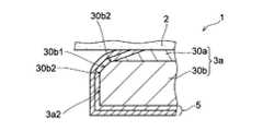
図1~図3に例示の配線基板1において導体層3は、図1では見易さのために簡略化されているが、図3に示されるように、金属膜30a及びめっき膜30bを含む2層構造を有している。金属膜30aは絶縁層2の表面2a上に形成されており、めっき膜30bは、金属膜30aにおける絶縁層2と反対側の表面上に形成されている。金属膜30aは、例えば無電解めっき又はスパッタリングなどで形成される。めっき膜30bは、例えば金属膜30aを給電層として用いる電解めっきによって形成される。図示されていないが、導体層33、絶縁層21又は絶縁層22上に形成されている導体層31及び導体層32、ビア導体2v、並びにスルーホール導体20cも、図3に示される導体層3と同様の2層構造を有し得る。 Theconductor layer 3 in thewiring board 1 illustrated in FIGS. 1 to 3 is simplified in FIG. 1 for ease of viewing, but includes ametal film 30a and aplating film 30b as shown in FIG. It has a two-layer structure. Themetal film 30a is formed on thesurface 2a of theinsulating layer 2, and theplated film 30b is formed on the surface of themetal film 30a opposite to theinsulating layer 2. As shown in FIG. Themetal film 30a is formed by, for example, electroless plating or sputtering. Theplated film 30b is formed, for example, by electrolytic plating using themetal film 30a as a power supply layer. Although not shown, theconductor layer 33, theconductor layers 31 and 32 formed on theinsulation layer 21 or theinsulation layer 22, thevia conductors 2v, and the through-hole conductors 20c are also connected to theconductor layer 3 shown in FIG. can have a two-layer structure similar to

各導体層は、所定の導体パッド及び/又は配線パターンを有するようにパターニングされている。図1の例の配線基板1では、導体層33は複数の部品実装パッド33aを有するようにパターニングされている。すなわち配線基板1は第1面11に形成されている複数の部品実装パッド33aを含んでいる。図1の例では、各部品実装パッド33aは、所謂SMDパッド(Solder Mask Defined)タイプの導体パッドである。すなわち、各部品実装パッド33aの周縁部がソルダーレジスト層40に覆われており、各部品実装パッド33aの周縁部以外の部分がソルダーレジスト層40の開口40aに露出している。 Each conductor layer is patterned to have predetermined conductor pads and/or wiring patterns. In thewiring board 1 in the example of FIG. 1, theconductor layer 33 is patterned to have a plurality ofcomponent mounting pads 33a. That is,wiring board 1 includes a plurality ofcomponent mounting pads 33 a formed onfirst surface 11 . In the example of FIG. 1, eachcomponent mounting pad 33a is a so-called SMD pad (Solder Mask Defined) type conductor pad. That is, the peripheral edge of eachcomponent mounting pad 33 a is covered with thesolder resist layer 40 , and the portion other than the peripheral edge of eachcomponent mounting pad 33 a is exposed through theopening 40 a of thesolder resist layer 40 .

各部品実装パッド33aは、配線基板1の使用時に配線基板1に実装される部品E1がその表面に載置される導体パッド(第2導体パッド)である。すなわち第1面11は配線基板1の部品実装面である。部品実装パッド33aには、例えばはんだなどの接合材(図示せず)を介して部品E1の電極E11が電気的及び機械的に接続される。 Eachcomponent mounting pad 33a is a conductor pad (second conductor pad) on which a component E1 to be mounted on thewiring board 1 is mounted when thewiring board 1 is used. That is, thefirst surface 11 is the component mounting surface of thewiring board 1 . Electrodes E11 of the component E1 are electrically and mechanically connected to thecomponent mounting pads 33a via a bonding material (not shown) such as solder.

部品E1としては、例えば、半導体集積回路装置やトランジスタなどの能動部品、及び、電気抵抗などの受動部品のような電子部品が例示される。部品E1は、半導体基板上に形成された微細配線を含む配線材であってもよい。しかし、部品E1はこれらに限定されない。 Examples of the components E1 include active components such as semiconductor integrated circuit devices and transistors, and electronic components such as passive components such as electrical resistors. The component E1 may be a wiring material including fine wiring formed on a semiconductor substrate. However, the part E1 is not limited to these.

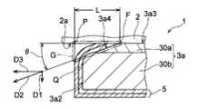
本実施形態では、導体層3は導体パッド3a(第1導体パッド)を含んでいる。図1~3に示されるように、導体パッド3aは、ソルダーレジスト層4の開口4aによって露出されている。具体的には、導体パッド3aにおける絶縁層2と反対側を向く表面3a1(第1主面)、及び導体パッド3aの側面3a2全体がソルダーレジスト層4に覆われずに露出している。すなわち、導体パッド3aは、その外縁がソルダーレジスト層の開口によって画定されない、所謂NSMDパッド(Non-Solder Mask Defined)タイプの導体パッドである。なお導体パッド3aの側面3a2は、導体パッド3aにおける絶縁層2を向く表面3a3(第2主面)と表面3a1との間の表面であって平面視において導体パッド3aの外縁を構成する表面である。なお「平面視」は、導体パッド3aなどの対象物をZ方向と平行な視線で見ることを意味している。導体パッド3aの表面3a3は、以下では、「導体パッド3aの背面3a3」とも称される。 In this embodiment, theconductor layer 3 includes aconductor pad 3a (first conductor pad). As shown in FIGS. 1 to 3, theconductor pads 3a are exposed throughopenings 4a in the solder resistlayer 4. FIG. Specifically, the surface 3a1 (first main surface) of theconductor pad 3a facing away from the insulatinglayer 2 and the entire side surface 3a2 of theconductor pad 3a are not covered with the solder resistlayer 4 and are exposed. That is, theconductor pad 3a is a so-called NSMD pad (Non-Solder Mask Defined) type conductor pad whose outer edge is not defined by an opening in the solder resist layer. The side surface 3a2 of theconductor pad 3a is a surface between the surface 3a3 (second main surface) facing the insulatinglayer 2 and the surface 3a1 of theconductor pad 3a, and constitutes the outer edge of theconductor pad 3a in plan view. be. Note that "planar view" means viewing an object such as theconductor pad 3a with a line of sight parallel to the Z direction. The front surface 3a3 of thecontact pad 3a is hereinafter also referred to as the "back surface 3a3 of thecontact pad 3a".

図1の例の配線基板1において、第2面12は、第1面11と同様に半導体集積回路装置のような電子部品が実装される部品実装面であってもよい。また第2面12は、外部の配線基板、例えば任意の電気機器のマザーボードなどの外部要素E2に配線基板1自体が実装される場合に、外部要素E2に接続される接続面であってもよい。すなわち、配線基板1は、例えば第1面11に実装される半導体集積回路などの部品E1のパッケージの一部を構成してもよい。その場合、配線基板1は、図1に示されるように第2面12を外部要素E2に向けて、外部要素E2に部品E1と共に実装されてもよい。 In thewiring substrate 1 shown in FIG. 1, thesecond surface 12 may be a component mounting surface on which electronic components such as a semiconductor integrated circuit device are mounted, similar to thefirst surface 11 . Also, thesecond surface 12 may be a connection surface that is connected to an external element E2 when thewiring board 1 itself is mounted on an external element E2 such as an external wiring board, for example, a motherboard of any electrical equipment. . That is, thewiring board 1 may form part of a package for a component E1 such as a semiconductor integrated circuit mounted on thefirst surface 11, for example. In that case, thewiring board 1 may be mounted with the component E1 on the external element E2 with thesecond surface 12 facing the external element E2 as shown in FIG.

第2面12が外部要素E2との接続面である場合、第2面12は外部要素E2との接続部を備え得る。図1の例の配線基板1は導体パッド3aにおいて外部要素E2と接続される。従って図1の例の導体パッド3aは、配線基板1において外部要素E2に接続される接続パッドであり、図1の配線基板1における外部要素E2との接続パッドは導体パッド3aからなる。前述したように、導体パッド3aの表面3a1の全体及び側面3a2の全体がソルダーレジスト層4に覆われずに開口4a内に露出している。従って、配線基板1と外部要素E2とが大きな面積で強固に接続され得る。 If thesecond surface 12 is the connection surface with the external element E2, thesecond surface 12 may comprise a connection with the external element E2. Thewiring board 1 in the example of FIG. 1 is connected to the external element E2 at theconductor pads 3a. Therefore, theconductor pad 3a in the example of FIG. 1 is a connection pad to be connected to the external element E2 on thewiring board 1, and the connection pad to the external element E2 on thewiring board 1 of FIG. 1 consists of theconductor pad 3a. As described above, the entire surface 3a1 and side surface 3a2 of theconductor pad 3a are not covered with the solder resistlayer 4 and are exposed in theopening 4a. Therefore, thewiring board 1 and the external element E2 can be firmly connected over a large area.

配線基板1の導体パッド3aは、図2に示されるように矩形の平面形状を有している。「平面形状」は、導体パッド3aのような対象物の平面視における形状である。ここで「矩形」は、互いに平行な2つの辺(線分)と、その2つの辺に直交する互いに平行な2つの辺(線分)とによって囲まれる形状を意味している。この「矩形」において、互いに隣接すると共に直交する二辺は、必ずしもその交点において直角の交角をなすように互いに接していなくてもよく、その交点付近の部分(角部)が、C面取り又はR面取りなどで面取りされた形状を有していてもよい。その場合、上記及び下記の説明における「矩形」の各一辺の直線部分は、好ましくは、その一辺と直交する他の二辺間の距離の1/3以上の長さを有している。図2の例の導体パッド3aでは、平面視における導体パッド3aの4つの角部はいずれもR面取りされている。 Theconductor pads 3a of thewiring board 1 have a rectangular planar shape as shown in FIG. The "planar shape" is the shape of an object, such as thecontact pad 3a, in plan view. Here, "rectangle" means a shape surrounded by two mutually parallel sides (line segments) and two mutually parallel sides (line segments) orthogonal to the two sides. In this "rectangle", the two sides that are adjacent and orthogonal to each other may not necessarily contact each other so as to form a right angle at the intersection, and the portion (corner) near the intersection is chamfered or R It may have a chamfered shape by chamfering or the like. In that case, each straight line portion of one side of the "rectangle" in the above and below description preferably has a length of 1/3 or more of the distance between the other two sides perpendicular to that one side. In theconductor pad 3a in the example of FIG. 2, all four corners of theconductor pad 3a in plan view are rounded.

導体パッド3aは、例えば、はんだなどの接合材B(図3参照)によって外部要素E2の電極E21に電気的及び機械的に接続され得る。外部要素E2は、前述したように、任意の電気機器を構成するマザーボードであってもよく、配線基板1よりも大きなパッケージサイズを有する任意の電子部品であってもよい。導体パッド3aは、これらに限定されない任意の基板、電気部品、又は機構部品などと接続され得る。 Theconductor pads 3a can be electrically and mechanically connected to the electrodes E21 of the external element E2 by a bonding material B (see FIG. 3) such as solder. As described above, the external element E2 may be a motherboard constituting any electrical equipment, or any electronic component having a package size larger than that of thewiring board 1. FIG. Thecontact pads 3a can be connected to any substrate, electrical component, mechanical component, or the like, but not limited to these.

図1の例では、導体パッド3aは、第1面11側に設けられている複数の部品実装パッド33aのいずれよりも大きい。例えば、部品E1よりも大きな外部要素E2と配線基板1とが、大きな面積で強固に接続されると考えられる。 In the example of FIG. 1, theconductor pad 3a is larger than any of the plurality ofcomponent mounting pads 33a provided on thefirst surface 11 side. For example, it is considered that the external element E2, which is larger than the component E1, and thewiring board 1 are firmly connected over a large area.

図1及び図2では省略されているが、配線基板1は、図3に示されるように導体パッド3aの表面3a1及び側面3a2を覆う表面処理層5を含んでいる。表面処理層5は、例えば導体パッド3aの表面3a1及び側面3a2などの露出部分の防食処理及び/又は防錆処理によって形成される被膜である。表面処理層5によって、導体パッド3aの腐食や酸化などが防がれる。 Although omitted in FIGS. 1 and 2, thewiring substrate 1 includes asurface treatment layer 5 covering the surface 3a1 and the side surface 3a2 of theconductor pad 3a as shown in FIG. Thesurface treatment layer 5 is, for example, a film formed by anticorrosion treatment and/or antirust treatment on exposed portions such as the surface 3a1 and the side surface 3a2 of theconductor pad 3a. Thesurface treatment layer 5 prevents corrosion and oxidation of theconductor pads 3a.

表面処理層5は、例えば、導体パッド3aとは異なる金属を含む金属被膜や、イミダゾール化合物などの有機物を含む有機被膜である。導体パッド3aが銅で形成されている場合、表面処理層5は、ニッケル、パラジウム、銀、金、若しくはこれらの合金、又ははんだなどによって形成され得る。図3の例では、表面処理層5は、導体パッド3aの本体側に形成されている下層51と下層51上に形成されている上層52とを含む2層構造を有している。下層51は、例えばニッケル膜若しくはニッケルとパラジウムとの合金膜であり、上層は、例えば金からなる金属膜である。 Thesurface treatment layer 5 is, for example, a metal coating containing a metal different from that of theconductive pads 3a, or an organic coating containing an organic substance such as an imidazole compound. When theconductor pads 3a are made of copper, thesurface treatment layer 5 can be made of nickel, palladium, silver, gold, alloys thereof, solder, or the like. In the example of FIG. 3, thesurface treatment layer 5 has a two-layer structure including alower layer 51 formed on the main body side of theconductor pad 3a and anupper layer 52 formed on thelower layer 51. As shown in FIG. Thelower layer 51 is, for example, a nickel film or an alloy film of nickel and palladium, and the upper layer is a metal film made of, for example, gold.

図3に示されるように、実施形態の配線基板1では、導体パッド3aの縁部が絶縁層2の表面2aから離間している。なお、導体パッド3aの「縁部」は、導体パッド3aの平面形状の外縁に沿って導体パッド3aの中央部を連続的又は断続的に囲む枠状の部分である。導体パッド3aの「縁部」は、導体パッド3aの外縁からの距離が長さLW以下の領域であり、各辺の幅として長さLWを有する枠状の部分である。長さLWは、例えば、0.01×LD以上、0.1×LD以下である。ここで「LD」は、長さLWと平行な方向において対向する導体パッド3aの二辺間の距離である。 As shown in FIG. 3, in thewiring board 1 of the embodiment, the edges of theconductor pads 3a are separated from thesurface 2a of the insulatinglayer 2. As shown in FIG. The “edge portion” of theconductor pad 3a is a frame-like portion that continuously or intermittently surrounds the central portion of theconductor pad 3a along the outer edge of the planar shape of theconductor pad 3a. The "edge" of theconductor pad 3a is a frame-shaped area having a length LW or less from the outer edge of theconductor pad 3a and having a width of each side of the length LW. The length LW is, for example, 0.01×LD or more and 0.1×LD or less. Here, "LD" is the distance between two sides of theconductor pads 3a facing each other in the direction parallel to the length LW.

図4には、配線基板1における導体パッド3aの縁部の断面(例えば図3のIV部)の拡大図が示されている。図4に示されるように、導体パッド3aの縁部は絶縁層2の表面2aから離れている。換言すると、導体パッド3aの縁部では、導体パッド3aが絶縁層2の表面2aから浮き上がっている。導体パッド3aの背面3a3と側面3a2とで構成される角部が切り欠かれている。そのため、図4に示される断面図では、導体パッド3aと絶縁層2の表面2aとの間に、二点鎖線で囲まれている切り欠き状の空間Gが形成されている。 FIG. 4 shows an enlarged view of a cross section of the edge of theconductor pad 3a on the wiring board 1 (for example, IV in FIG. 3). As shown in FIG. 4, the edges of theconductor pads 3a are spaced apart from thesurface 2a of the insulatinglayer 2. As shown in FIG. In other words, the edge of theconductor pad 3a is raised from thesurface 2a of the insulatinglayer 2. As shown in FIG. The corner formed by the rear surface 3a3 and the side surface 3a2 of theconductor pad 3a is notched. Therefore, in the cross-sectional view shown in FIG. 4, a notch-like space G surrounded by a two-dot chain line is formed between theconductor pad 3a and thesurface 2a of the insulatinglayer 2. As shown in FIG.

導体パッド3aの縁部が絶縁層2の表面2aから離れているため、導体パッド3aの側面3a2と、その背面3a3と絶縁層2の表面2aとの界面の外縁(この界面の外縁は単に「外縁F」とも称される)とは、表面2aの垂直方向において一列に並んでいない。すなわち、側面3a2と外縁Fとは平面視で重なっていない。外縁Fは、側面3a2よりも導体パッド3aの内側(中央側)に位置している。また、導体パッド3aの縁部が絶縁層2の表面2aから離れているため、導体パッド3aの側面3a2の下端Q(絶縁層2側の先端)は、表面2aと接しておらず、表面2aから離れている。 Since the edge of theconductor pad 3a is separated from thesurface 2a of the insulatinglayer 2, the outer edge of the interface between the side surface 3a2 of theconductor pad 3a, its back surface 3a3, and thesurface 2a of the insulating layer 2 (the outer edge of this interface is simply " The outer edges F") are not aligned in the vertical direction of thesurface 2a. That is, the side surface 3a2 and the outer edge F do not overlap in plan view. The outer edge F is located inside (center side) of theconductor pad 3a with respect to the side surface 3a2. In addition, since the edge of theconductor pad 3a is separated from thesurface 2a of the insulatinglayer 2, the lower end Q (tip on the side of the insulating layer 2) of the side surface 3a2 of theconductor pad 3a is not in contact with thesurface 2a. away from

前述したように、従来の配線基板において導体パッド及びその下層の絶縁層には、両者の間の熱膨張率の相違や外力などによって応力が生じることがある。その応力は、絶縁層の表面上において導体パッドが存在する領域と存在しない領域との境界となる導体パッドの縁部に集中し易い。またこの応力は、絶縁層と導体パッドとの界面の外縁(図4の例では外縁F)から、絶縁層から離れる方向に延びる導体パッドの表面(例えば導体パッドの側面)に沿った方向に作用し易いと考えられる。従って、本実施形態と異なり導体パッドの縁部がその下層の絶縁層の表面から離れていない場合、集中する応力は、導体パッドの側面に沿った方向、すなわち、導体パッドの下層の絶縁層の表面と直交する方向に強く作用すると考えられる。そして、その絶縁層の表面と直交する方向に強く作用する応力によって、絶縁層における導体パッドの側面と接する部分にクラックが生じたり、導体パッドの外縁を発端とする絶縁層と導体パッドとの界面剥離が生じたりすることがある。 As described above, in the conventional wiring board, stress may be generated in the conductor pad and the insulating layer therebelow due to the difference in thermal expansion coefficient between them or external force. The stress tends to concentrate on the edge of the conductor pad, which is the boundary between the area where the conductor pad exists and the area where the conductor pad does not exist on the surface of the insulating layer. Moreover, this stress acts in a direction along the surface of the conductor pad (for example, the side surface of the conductor pad) extending away from the insulation layer from the outer edge of the interface between the insulating layer and the conductor pad (outer edge F in the example of FIG. 4). is considered to be easy. Therefore, unlike the present embodiment, if the edge of the conductor pad is not separated from the surface of the underlying insulation layer, the concentrated stress is directed along the side surface of the conductor pad, i.e., It is believed to act strongly in the direction perpendicular to the surface. The stress acting strongly in the direction perpendicular to the surface of the insulating layer may cause cracks in the insulating layer in contact with the side surfaces of the conductive pads, or the interface between the insulating layer and the conductive pads starting from the outer edges of the conductive pads. Delamination may occur.

これに対して本実施形態では、導体パッド3aの縁部は絶縁層2の表面2aから離間している。そして導体パッド3aにおいて、絶縁層2の表面2aから離れる方向に外縁Fから延びる表面3a4は、絶縁層2の表面2aに直交する方向D1に対して傾いた方向D2に沿って延びている。すなわち、絶縁層2の表面2aと接していて表面2aから離れる方向に延びる導体パッド3aの表面3a4は、表面2aに対して直角よりも小さい角度θをなして表面2aに接している。そのため、導体パッド3aの縁部に集中し易い応力は、方向D1ではなく方向D1に対して傾いた方向D2に強く作用すると考えられる。そしてその方向D2に作用する応力は、絶縁層2の表面2aに直交する方向D1だけでなく、方向D1に直交する方向D3にも分散して作用すると考えられる。すなわち、絶縁層2に対してその表面2aに直交する方向D1に作用する応力が、導体パッドの縁部が下層の絶縁層の表面から離間していない場合と比べて軽減されると考えられる。従って、本実施形態では、絶縁層2におけるクラックの発生や、絶縁層2と導体パッド3aとの界面剥離などが抑制されると考えられる。 On the other hand, in this embodiment, the edge of theconductor pad 3a is separated from thesurface 2a of the insulatinglayer 2. FIG. In theconductor pad 3a, a surface 3a4 extending from the outer edge F in a direction away from thesurface 2a of the insulatinglayer 2 extends along a direction D2 inclined with respect to a direction D1 perpendicular to thesurface 2a of the insulatinglayer 2. FIG. That is, the surface 3a4 of theconductor pad 3a, which is in contact with thesurface 2a of the insulatinglayer 2 and extends away from thesurface 2a, is in contact with thesurface 2a at an angle .theta. Therefore, it is considered that the stress that tends to concentrate on the edge of theconductor pad 3a acts strongly not in the direction D1 but in the direction D2 tilted with respect to the direction D1. It is considered that the stress acting in the direction D2 acts not only in the direction D1 orthogonal to thesurface 2a of the insulatinglayer 2 but also in the direction D3 orthogonal to the direction D1. That is, the stress acting on insulatinglayer 2 in direction D1 perpendicular tosurface 2a is reduced compared to the case where the edge of the conductor pad is not separated from the surface of the underlying insulating layer. Therefore, in the present embodiment, cracks in the insulatinglayer 2 and interfacial separation between the insulatinglayer 2 and theconductor pads 3a are suppressed.

特に図1~図4に例示される配線基板1では、前述したように導体パッド3aは、第1面11側に設けられている複数の部品実装パッド33aのいずれよりも大きい。従って、その平面面積は大きく、導体パッド3aは絶縁層2との間に比較的大きな界面を有し得る。従って導体パッド3aの縁部に集中する応力も過大になり易い。導体パッド3aのように比較的大きな平面面積を有する導体パッドにおいて本実施形態は特に有益であると考えられる。 Particularly, in thewiring board 1 illustrated in FIGS. 1 to 4, theconductor pad 3a is larger than any of the plurality ofcomponent mounting pads 33a provided on thefirst surface 11 side, as described above. Therefore, its plane area is large, and thecontact pad 3a can have a relatively large interface with the insulatinglayer 2. FIG. Therefore, the stress concentrated on the edge of theconductor pad 3a tends to become excessive. It is believed that this embodiment is particularly beneficial for conductor pads having a relatively large planar area, such asconductor pad 3a.

導体パッド3aの表面3a4と絶縁層2の表面2aとの間の角度θは、0°よりも大きく90°よりも小さい。例えば、角度θは、10°以上、80°以下である。 The angle θ between the surface 3a4 of theconductor pad 3a and thesurface 2a of the insulatinglayer 2 is larger than 0° and smaller than 90°. For example, the angle θ is 10° or more and 80° or less.

導体パッド3aの縁部における絶縁層2の表面2aから離間している部分の表面2a上での長さL(平面視における側面3a2から外縁Fまでの距離)は、導体パッド3aを介して外縁Fに伝わる外力の緩和の観点からは長い方が好ましい。一方で、導体パッド3aと絶縁層2との密着強度の観点では、長さLは短い方が好ましいと考えられる。長さLは、外縁Fに伝わる外力の緩和と導体パッド3aの密着強度の確保との両方が適切に実現されるように、例えば、3μm以上、10μm以下である。 The length L on thesurface 2a of the portion spaced from thesurface 2a of the insulatinglayer 2 at the edge of theconductor pad 3a (the distance from the side surface 3a2 to the outer edge F in plan view) is the outer edge through theconductor pad 3a. From the viewpoint of mitigation of the external force transmitted to F, the longer one is preferable. On the other hand, from the viewpoint of the adhesion strength between theconductor pads 3a and the insulatinglayer 2, it is considered that the shorter the length L, the better. The length L is, for example, 3 μm or more and 10 μm or less so that both the relaxation of the external force transmitted to the outer edge F and the securing of the adhesion strength of theconductor pads 3a are appropriately achieved.

図4の例では、互いから離間している導体パッド3aの縁部と絶縁層2の表面2aとの間隔は、導体パッド3aの外周に向かって拡大している。換言すると、導体パッド3aの縁部を表面2aから離間させている切り欠き状の空間Gの高さ(表面2aからの高さ)は、導体パッド3aの外周に向かうほど高くなっている。すなわち、導体パッド3aにおける絶縁層2の表面2aからの離間部分の表面が、側面3a2や背面3a3と略平行や略直角ではなく傾いている。そのため、前述したように、絶縁層2から離間している導体パッド3aの縁部と絶縁層2との界面に導体パッド3aの熱収縮などによって加わり得る剥離方向の力が、その界面に沿った方向にも分散されると考えられる。導体パッド3aと絶縁層2との界面剥離などが生じ難いと推察される。 In the example of FIG. 4, the distance between the edges of theconductor pads 3a spaced apart from each other and thesurface 2a of the insulatinglayer 2 increases towards the periphery of theconductor pads 3a. In other words, the height (height from thesurface 2a) of the notched space G separating the edge of theconductor pad 3a from thesurface 2a increases toward the outer periphery of theconductor pad 3a. That is, the surfaces of the portions of theconductor pads 3a separated from thesurface 2a of the insulatinglayer 2 are not substantially parallel or substantially perpendicular to the side surface 3a2 or the rear surface 3a3, but are inclined. Therefore, as described above, the force in the peeling direction that can be applied to the interface between the edge of theconductor pad 3a separated from the insulatinglayer 2 and the insulatinglayer 2 due to the heat shrinkage of theconductor pad 3a is applied along the interface. It is thought that it is distributed also in the direction. It is presumed that peeling at the interface between theconductor pad 3a and the insulatinglayer 2 is unlikely to occur.

さらに図4の例では、導体パッド3aの背面3a3と側面3a2とによって構成される角部が丸まっている。そして、導体パッド3aにおいて絶縁層2から離間している縁部の表面は曲面を含んでいる。すなわち、導体パッド3aの縁部が絶縁層2の表面2aから離間していない場合における背面3a3と側面3a2との仮想の交線(図4における点P)付近が丸まっていて導体パッド3aはその交線付近の表面に曲面状の部分を有している。導体パッド3aの縁部が丸まっているので、絶縁層2だけでなく表面処理層5にもクラックが生じ難いと考えられる。 Furthermore, in the example of FIG. 4, the corner formed by the rear surface 3a3 and the side surface 3a2 of theconductor pad 3a is rounded. The surface of the edge of theconductor pad 3a that is spaced apart from the insulatinglayer 2 includes a curved surface. That is, when the edge of theconductor pad 3a is not separated from thesurface 2a of the insulatinglayer 2, the virtual intersection line (point P in FIG. 4) between the rear surface 3a3 and the side surface 3a2 is rounded, and theconductor pad 3a is rounded. It has a curved portion on the surface near the line of intersection. Since the edges of theconductor pads 3a are rounded, cracks are less likely to occur not only in the insulatinglayer 2 but also in thesurface treatment layer 5. FIG.

具体的には、導体パッド3aの側面3a2とめっき膜30bの下面(絶縁層2を向く表面)とによって構成されるべき角部が丸まっていて曲面状の表面を有している。一方、金属膜30aにおけるめっき膜30bと絶縁層2との間の端面は略平坦面であって、絶縁層2側ほど導体パッド3aの内周側に向かうように傾斜している。従って、導体パッド3aを構成する金属膜30aの端部も絶縁層2の表面2aから離間している。 Specifically, the corners to be formed by the side surface 3a2 of theconductor pad 3a and the lower surface of theplating film 30b (the surface facing the insulating layer 2) are rounded to form a curved surface. On the other hand, the end surface of themetal film 30a between theplating film 30b and the insulatinglayer 2 is a substantially flat surface, and is inclined toward the inner peripheral side of theconductor pad 3a toward the insulatinglayer 2 side. Therefore, the end of themetal film 30a forming theconductor pad 3a is also separated from thesurface 2a of the insulatinglayer 2. As shown in FIG.

なお表面処理層5が、導体パッド3aを構成する材料の熱膨張率と絶縁層2の熱膨張率の間の熱膨張率を用いて形成されると、表面処理層5が形成されない場合と比べて、絶縁層2及び導体パッド3aに生じる応力が低減されると考えられる。また、表面処理層5が、絶縁層2との熱膨張率の差が導体パッド3aよりも大きい材料で形成される場合でも、本実施形態では導体パッド3aの縁部が絶縁層2の表面2aから離間しているので、クラックなどの不具合が生じ難いと考えられる。 When thesurface treatment layer 5 is formed using a thermal expansion coefficient between the thermal expansion coefficient of the material forming theconductor pads 3a and the thermal expansion coefficient of the insulatinglayer 2, thesurface treatment layer 5 is not formed. Therefore, it is considered that the stress generated in the insulatinglayer 2 and theconductor pads 3a is reduced. Moreover, even if thesurface treatment layer 5 is formed of a material having a larger difference in coefficient of thermal expansion with the insulatinglayer 2 than theconductive pads 3a, in the present embodiment, the edges of theconductive pads 3a are located on thesurface 2a of the insulatinglayer 2. , it is considered that problems such as cracks are less likely to occur.

さらに図1~図4の例の配線基板1の導体パッド3aでは、前述したように平面視における4つの角部がR面取りされているので、R面取りのない導体パッドに比べて、導体パッド3aと絶縁層2との熱膨張率の違いなどによる応力集中箇所が少ない。従って、絶縁層2のクラックなどの不具合が一層生じ難いと考えられる。 Furthermore, in theconductor pads 3a of thewiring substrate 1 in the examples of FIGS. 1 to 4, as described above, the four corners in plan view are rounded, so that theconductor pads 3a are less than the conductor pads without the rounded chamfers. There are few places where stress is concentrated due to the difference in coefficient of thermal expansion between the insulatinglayer 2 and the insulatinglayer 2 . Therefore, it is considered that problems such as cracks in the insulatinglayer 2 are much less likely to occur.

本実施形態では、導体パッド3aは、所謂NSMDタイプの導体パッドであるため、導体パッド3aにおいて大きな露出部分が確保される。そのため導体パッド3aに接続される外部要素との広い接続面積が確保され、その外部要素と配線基板1とが強固に接続され得る。一方で、図1~図4を参照して説明が為されたように、導体パッド3aの縁部が絶縁層2から離間しているので、導体パッド3aの周辺部におけるクラックや界面剥離などの不具合が抑制され得る。 In the present embodiment, theconductor pad 3a is a so-called NSMD type conductor pad, so a large exposed portion is secured in theconductor pad 3a. Therefore, a wide connection area with an external element connected to theconductor pad 3a is ensured, and the external element and thewiring substrate 1 can be firmly connected. On the other hand, as described with reference to FIGS. 1 to 4, since the edge of theconductor pad 3a is separated from the insulatinglayer 2, cracks and interfacial peeling at the periphery of theconductor pad 3a do not occur. Defects can be suppressed.

図5A及び図5Bには、それそれ、導体パッド3aの縁部の他の例が示されている。図5Aの例では、導体パッド3aは、絶縁層2から離間する縁部において、金属膜30aの表面だけでなくめっき膜30bの表面にも平坦部30b1を有している。図5Aの例の導体パッド3aの縁部の表面は、平坦部30b1と側面3a2との間、及び平坦部30b1とめっき膜30bにおける絶縁層2側の表面との間それぞれに曲面部30b2を有している。2つの曲面部30b2によって、平坦部30b1と側面3a2、及び、めっき膜30bにおける絶縁層2側の表面と平坦部30b1が滑らかに繋がれている。図5Aの例においても、絶縁層2及び/又は表面処理層5にクラックなどの不具合が生じ難いと考えられる。 5A and 5B respectively show other examples of the edge of thecontact pad 3a. In the example of FIG. 5A, theconductor pad 3a has a flat portion 30b1 on the surface of themetal film 30a as well as on the surface of theplating film 30b at the edge spaced apart from the insulatinglayer 2. In the example of FIG. The edge surface of theconductor pad 3a in the example of FIG. 5A has curved surface portions 30b2 between the flat portion 30b1 and the side surface 3a2 and between the flat portion 30b1 and the surface of theplating film 30b on the insulatinglayer 2 side. is doing. The flat portion 30b1 and the side surface 3a2, and the surface of theplating film 30b on the insulatinglayer 2 side and the flat portion 30b1 are smoothly connected by the two curved surface portions 30b2. In the example of FIG. 5A as well, problems such as cracks are unlikely to occur in the insulatinglayer 2 and/or thesurface treatment layer 5 .

図5Bの例の導体パッド3aは、図5Aの例の導体パッド3aと同様に、めっき膜30bの表面上に平坦部30b1を有しているが、図5Aに示される曲面部30b2を備えていない。しかし、図5Bの例においても、導体パッド3aの縁部は絶縁層2の表面2aから離間している。従って、導体パッド3aの縁部が表面2aから離間していない場合に表面2aに直交する方向に作用する力が軽減されると考えられる。従って、図5Bの例においても、絶縁層2にクラックなどの不具合が生じ難いと考えられる。 Theconductive pad 3a in the example of FIG. 5B has a flat portion 30b1 on the surface of theplating film 30b, like theconductive pad 3a in the example of FIG. 5A, but has a curved portion 30b2 shown in FIG. 5A. do not have. However, even in the example of FIG. 5B, the edge of theconductor pad 3a is spaced from thesurface 2a of the insulatinglayer 2. As shown in FIG. Therefore, it is considered that the force acting in the direction perpendicular to thesurface 2a is reduced when the edge of theconductor pad 3a is not separated from thesurface 2a. Therefore, in the example of FIG. 5B as well, problems such as cracks are unlikely to occur in the insulatinglayer 2 .

実施形態の配線基板は、任意の一般的な配線基板の製造方法によって製造され得る。図6A~図6Gを参照して、図1に示される配線基板1が製造される場合を例に、製造方法の一例が概説される。 The wiring board of the embodiment can be manufactured by any general wiring board manufacturing method. An example of a manufacturing method will be outlined with reference to FIGS. 6A to 6G, taking as an example the case where thewiring board 1 shown in FIG. 1 is manufactured.

図6Aに示されるように、コア基板10が用意され、コア基板10の一面10a側に絶縁層21が積層され、その絶縁層21上に導体層31が形成される。同様に、コア基板10の他面10b側に、絶縁層22が積層され、その絶縁層22上に導体層32が形成される。そしてコア基板10の両面において、各絶縁層の積層と導体層の形成とが繰り返され、コア基板10の一面10a側及び他面10b側に、最表層の絶縁層23及び最表層の絶縁層2が形成される。 As shown in FIG. 6A,core substrate 10 is prepared, insulatinglayer 21 is laminated on onesurface 10 a ofcore substrate 10 , andconductor layer 31 is formed on insulatinglayer 21 . Similarly, an insulatinglayer 22 is laminated on theother surface 10 b side of thecore substrate 10 , and aconductor layer 32 is formed on the insulatinglayer 22 . Lamination of each insulating layer and formation of conductor layers are repeated on both surfaces of thecore substrate 10 , and an outermost insulatinglayer 23 and an outermost insulatinglayer 2 are formed on the onesurface 10 a side and theother surface 10 b side of thecore substrate 10 . is formed.

コア基板10の用意では、例えば、絶縁層20を含む両面銅張積層板が用意される。そしてサブトラクティブ法などによって所定の導体パターンを含む導体層31、32を絶縁層20の両面に形成すると共にスルーホール導体20cを絶縁層20内に形成することによってコア基板10が用意される。絶縁層21、22、及び、絶縁層21又は絶縁層22上の導体層31、32は、例えば一般的なビルドアップ基板の製造方法によって、それぞれ形成される。例えば各絶縁層は、フィルム上のエポキシ樹脂を、コア基板10又は先に形成されている各絶縁層及び各導体層上に熱圧着することによって形成される。また、各導体層は、例えば、めっきレジストの形成及びパターンめっきなどを含むセミアディティブ法やフルアディティブ法などの導体パターンの任意の形成方法を用いて形成される。セミアディティブ法などの導体パターンの形成方法を用いる各導体層の形成では、ビア導体2vが各絶縁層内に形成され得る。 In preparing thecore substrate 10, for example, a double-sided copper-clad laminate including an insulatinglayer 20 is prepared. Conductor layers 31 and 32 including predetermined conductor patterns are formed on both surfaces of the insulatinglayer 20 by a subtractive method or the like, and a through-hole conductor 20c is formed in the insulatinglayer 20 to prepare thecore substrate 10. FIG. The insulating layers 21 and 22 and the conductor layers 31 and 32 on the insulatinglayer 21 or the insulatinglayer 22 are formed by, for example, a general build-up board manufacturing method. For example, each insulating layer is formed by thermocompression bonding an epoxy resin film on thecore substrate 10 or previously formed insulating layers and conductor layers. Moreover, each conductor layer is formed by using any method for forming a conductor pattern, such as a semi-additive method or a full-additive method including formation of a plating resist and pattern plating. In forming each conductor layer using a method for forming a conductor pattern such as a semi-additive method, viaconductors 2v can be formed in each insulating layer.

図6Bに示されるように、絶縁層2の表面2a上、及びレーザー光の照射などによって形成された絶縁層2の貫通孔内に無電解めっき又はスパッタリングなどによって金属膜30aが形成される。コア基板10の一面10a側にも同様に金属膜30aが形成される。 As shown in FIG. 6B, ametal film 30a is formed by electroless plating, sputtering, or the like on thesurface 2a of the insulatinglayer 2 and in the through holes of the insulatinglayer 2 formed by laser light irradiation or the like. Ametal film 30a is also formed on the onesurface 10a side of thecore substrate 10 in the same manner.

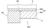
図6B及び図6Cに示されるように、金属膜30a上に、めっきレジストPRが設けられる。図6Cには、図6BのVIC部の拡大図が示されている。絶縁層2の上に設けられるめっきレジストPRには、導体層3(図6E参照)に含まれるべき導体パターンに対応する領域に開口PR1が形成される。 As shown in FIGS. 6B and 6C, a plating resist PR is provided on themetal film 30a. FIG. 6C shows an enlarged view of the VIC portion of FIG. 6B. In the plating resist PR provided on the insulatinglayer 2, an opening PR1 is formed in a region corresponding to the conductor pattern to be included in the conductor layer 3 (see FIG. 6E).

各開口PR1を備えるめっきレジストPRは、フォトリソグラフィ技術を用いて形成される。まず、例えばネガ型の感光性樹脂フィルムを金属膜30a上の全面に積層することによって、めっきレジストPRとなるレジスト膜が形成される。そして、レジスト膜における開口PR1が形成されるべき領域を覆う露光マスクEMが、レジスト膜上に配置される。 A plating resist PR having each opening PR1 is formed using a photolithographic technique. First, for example, by laminating a negative type photosensitive resin film on the entire surface of themetal film 30a, a resist film to be the plating resist PR is formed. Then, an exposure mask EM covering a region of the resist film where the opening PR1 is to be formed is placed on the resist film.

図6Cに示されるように、例えば紫外線Uが、露光マスクEMを通してめっきレジストPRとなるレジスト膜に照射される。レジスト膜のうちの露光マスクEMに覆われていない露光部分PRaが架橋反応によって不溶性に変化する。一方、レジスト膜のうち露光マスクEMに覆われている非露光部分PRbの大部分は溶解性のまま変化しない。しかし露光マスクEMの真下の部分のうち、金属膜30a及び露光部分PRaの両方に近接する境界部分BPは、金属膜30aで反射した紫外光Uによって露光されて不溶性へと変化する。その後、露光マスクEMが除去され、非露光部分PRbが現像によって除去される。しかし、境界部分BPは露光部分PRaと共に残存する。その結果、境界部分BPによって金属膜30aに近接する部分が拡幅されたマスク部を有するめっきレジストPRが形成される。境界部分BPは、例えば、金属膜30aの表面を粗化して紫外線Uを適度に乱反射させることによって形成され得る。なお、以下の説明では、境界部分BPは、めっきレジストPRの「拡幅部分BP」とも称される。 As shown in FIG. 6C, for example, an ultraviolet ray U is irradiated through an exposure mask EM to a resist film to be a plating resist PR. The exposed portion PRa of the resist film, which is not covered with the exposure mask EM, becomes insoluble due to the cross-linking reaction. On the other hand, most of the unexposed portion PRb covered with the exposure mask EM in the resist film remains soluble. However, the boundary portion BP adjacent to both themetal film 30a and the exposed portion PRa among the portions immediately below the exposure mask EM is exposed to the ultraviolet light U reflected by themetal film 30a and becomes insoluble. After that, the exposure mask EM is removed, and the non-exposed portion PRb is removed by development. However, the boundary portion BP remains together with the exposed portion PRa. As a result, a plating resist PR is formed having a mask portion in which a portion adjacent to themetal film 30a is widened by the boundary portion BP. The boundary portion BP can be formed, for example, by roughening the surface of themetal film 30a to diffusely reflect the ultraviolet rays U appropriately. In the following description, the boundary portion BP is also referred to as the "widened portion BP" of the plating resist PR.

図6Dに示されるように、めっきレジストPRの開口PR1内に、金属膜30aを給電層として用いる電解めっきによって導体層3の各導体パターンが形成される。図6Dに示される開口PR1には、導体層3の導体パッド3aを構成するめっき膜30bが形成される。図6Dに示されるように、縁部における金属膜30aに近接する部分がめっきレジストPRの拡幅部分BPによって切り欠かれためっき膜30bが形成される。その後、めっきレジストPRが除去される。 As shown in FIG. 6D, each conductor pattern of theconductor layer 3 is formed in the opening PR1 of the plating resist PR by electroplating using themetal film 30a as a power supply layer. A platedfilm 30b forming aconductor pad 3a of theconductor layer 3 is formed in the opening PR1 shown in FIG. 6D. As shown in FIG. 6D, a platedfilm 30b is formed in which the edge portion adjacent to themetal film 30a is notched by the widened portion BP of the plating resist PR. After that, the plating resist PR is removed.

図6E及び図6Fに示されるように、めっきレジストの除去によって露出する金属膜30aの不要部分がフラッシュエッチングなどによって除去される。導体パッド3aなどの所定の導体パターンを有する導体層3が形成される。コア基板10の一面10a側には、所定の導体パターンを有する導体層33が形成される。なお、図6Fには、図6EのVIF部の拡大図が示されている。 As shown in FIGS. 6E and 6F, unnecessary portions of themetal film 30a exposed by removing the plating resist are removed by flash etching or the like. Aconductor layer 3 having a predetermined conductor pattern such as aconductor pad 3a is formed. Aconductor layer 33 having a predetermined conductor pattern is formed on the onesurface 10a side of thecore substrate 10 . Note that FIG. 6F shows an enlarged view of the VIF portion of FIG. 6E.

図6Fに示されるように、導体パッド3aを構成する金属膜30aの端面30a1(図4における導体パッド3aの表面3a4)では、絶縁層2側の方がめっき膜30b側よりも多く除去されている。その結果、端面30a1は、絶縁層2側ほど導体パッド3aの内周側に向かうように傾斜している。めっき膜30bの縁部における金属膜30aとの近傍部分を切り欠かれた形状とすることによって、エッチング液の回り込みに関して絶縁層2側とめっき膜30b側との間において異なる状況を作り出すことができる。その結果、図6Fに示されるように端面30a1を傾斜させることができる。 As shown in FIG. 6F, on the end face 30a1 of themetal film 30a forming theconductor pad 3a (the surface 3a4 of theconductor pad 3a in FIG. 4), theinsulation layer 2 side is removed more than theplating film 30b side. there is As a result, the end surface 30a1 is inclined toward the inner peripheral side of theconductor pad 3a toward the insulatinglayer 2 side. By making the edge portion of theplating film 30b and the vicinity of themetal film 30a into a notched shape, it is possible to create a different situation between the insulatinglayer 2 side and theplating film 30b side with respect to the wraparound of the etchant. . As a result, the end surface 30a1 can be inclined as shown in FIG. 6F.

図6Fの例では、めっき膜30bの縁部における金属膜30aとの近傍部分が切り欠かれたような形状を有しているため、導体パッド3aの縁部が絶縁層2の表面2aから離間している。さらに、金属膜30aの端面30a1が絶縁層2側ほど導体パッド3aの内周側に向かうように傾斜しているため、より長い範囲に渡って導体パッド3aの縁部が絶縁層2から離間している。 In the example of FIG. 6F, the edge of theplating film 30b has a shape in which the vicinity of themetal film 30a is notched. is doing. Furthermore, since the end surface 30a1 of themetal film 30a is inclined toward the inner peripheral side of theconductor pad 3a toward the insulatinglayer 2 side, the edge of theconductor pad 3a is separated from the insulatinglayer 2 over a longer range. ing.

なお、先に参照した図5A及び図5Bに示されるめっき膜30bの形状も、前述した金属膜30aの表面の粗化の調整や、紫外線の照射角度及び光度の調整によって形成し得ると考えられる。 It is considered that the shape of the platedfilm 30b shown in FIGS. 5A and 5B can also be formed by adjusting the roughening of the surface of themetal film 30a and adjusting the irradiation angle and luminous intensity of the ultraviolet rays. .

そして、図1に示されるように、ソルダーレジスト層40が絶縁層23及び導体層33上に形成され、ソルダーレジスト層4が絶縁層2及び導体層3上に形成される。ソルダーレジスト層4、40それぞれには、開口4a又は開口40aが設けられる。ソルダーレジスト層4、40は、それぞれ、例えば感光性のエポキシ樹脂又はポリイミド樹脂などを塗布したり噴霧したりフィルム状で積層したりすることによって形成される。そして、例えば露光及び現像、又はレーザー加工などによって、開口4a、40aが、それぞれ形成される。 Then, as shown in FIG. 1 , a solder resistlayer 40 is formed on the insulatinglayer 23 and theconductor layer 33 , and a solder resistlayer 4 is formed on the insulatinglayer 2 and theconductor layer 3 . Each of the solder resistlayers 4 and 40 is provided with anopening 4a or anopening 40a. The solder resistlayers 4 and 40 are each formed by coating or spraying a photosensitive epoxy resin or polyimide resin, or laminating them in a film form. Then, theopenings 4a and 40a are respectively formed by, for example, exposure and development, laser processing, or the like.

開口4a内に露出する導体パッド3aの表面上、及び開口40a内に露出する部品実装パッド33aの表面上には、表面処理層5(図3参照)が形成され得る。表面処理層5は、例えば、導体パッド3aの表面上及び部品実装パッド33aの表面上に、無電解めっき若しくは電解めっきなどによって、ニッケル、パラジウム、金などの金属を析出させること、又は、スプレーイングによって耐熱性の有機物を塗布することによって形成され得る。以上の工程を経ることによって図1の例の配線基板1が完成する。 A surface treatment layer 5 (see FIG. 3) can be formed on the surfaces of theconductor pads 3a exposed in theopenings 4a and on the surfaces of thecomponent mounting pads 33a exposed in theopenings 40a. Thesurface treatment layer 5 is formed, for example, by depositing a metal such as nickel, palladium, or gold on the surface of theconductor pad 3a and the surface of thecomponent mounting pad 33a by electroless plating or electrolytic plating, or by spraying. It can be formed by applying a heat-resistant organic material by Thewiring substrate 1 shown in FIG. 1 is completed through the above steps.

実施形態の配線基板は、各図面に例示される構造、並びに、本明細書において例示される構造、形状、及び材料を備えるものに限定されない。実施形態の配線基板は任意の積層構造を有し得る。例えば実施形態の配線基板はコア基板を含まないコアレス基板であってもよい。実施形態の配線基板は任意の数の導体層及び絶縁層を含み得る。実施形態の配線基板は所謂両面基板であってもよく、片面基板であってもよい。導体パターン3aは表面処理層5を備えなくてもよい。縁部において下層の絶縁層の表面から離間する導体パッドは、前述したように、配線基板の両方の表面に設けられていてもよく、いずれか一方の表面だけに設けられていてもよい。ソルダーレジスト層4は、開口4a内に導体パッド3aの全体を露出させながら、導体層3における導体パッド3a以外の部分を覆っていてもよい。部品実装パッド33aは、所謂NSMDパッドタイプの導体パッドであってもよい。導体パッド3aは、絶縁層2から離間する縁部において絶縁層2の表面2aとの間隔が略一定である平行部分を有していてもよい。また、平面視における導体パッド3aの角部は面取りされていなくてもよい。 The wiring substrates of the embodiments are not limited to those having the structures illustrated in each drawing, and the structures, shapes, and materials illustrated in this specification. The wiring board of the embodiment can have any laminated structure. For example, the wiring board of the embodiment may be a coreless board that does not include a core board. A wiring substrate of embodiments may include any number of conductor layers and insulating layers. The wiring board of the embodiment may be a so-called double-sided board or a single-sided board. Theconductor pattern 3a does not have to be provided with thesurface treatment layer 5. FIG. The conductor pads separated from the surface of the underlying insulating layer at the edges may be provided on both surfaces of the wiring substrate, or may be provided on only one of the surfaces, as described above. The solder resistlayer 4 may cover portions of theconductor layer 3 other than theconductor pads 3a while exposing theentire conductor pads 3a in theopenings 4a. Thecomponent mounting pads 33a may be so-called NSMD pad type conductor pads. Theconductor pads 3a may have parallel portions at the edges spaced apart from the insulatinglayer 2, the distances from thesurface 2a of the insulatinglayer 2 being substantially constant. Also, the corners of theconductor pads 3a in plan view may not be chamfered.

1 配線基板
11 第1面
12 第2面
2 絶縁層(第1絶縁層)
2a 表面
20~23 絶縁層
3 導体層
3a 導体パッド
3a1 表面
3a2 側面
3a3 表面(背面)
31~33 導体層
33a 部品実装パッド
4 ソルダーレジスト層(第1ソルダーレジスト層)
40 ソルダーレジスト層(第2ソルダーレジスト層)
4a、40a 開口
5 表面処理層
E2 外部要素
1 Wiringboard 11First surface 12Second surface 2 Insulating layer (first insulating layer)
2a surface 20-23insulating layer 3conductor layer 3a conductor pad 3a1 surface 3a2 side surface 3a3 surface (back surface)
31 to 33conductor layer 33acomponent mounting pad 4 solder resist layer (first solder resist layer)
40 solder resist layer (second solder resist layer)
4a,40a opening 5 surface treatment layer E2 external element

Claims (11)

Translated fromJapanese
第1絶縁層と、
前記第1絶縁層の表面上に形成されている導体層と、
前記第1絶縁層の前記表面上及び前記導体層上に形成されていて、前記導体層の少なくとも一部を露出させる開口を有するソルダーレジスト層と、
を含んでいて、第1面及び前記第1面の反対面である第2面を有する配線基板であって、
前記導体層は前記開口によって露出される導体パッドを含み、
前記導体パッドにおける前記第1絶縁層と反対側を向く表面及び前記導体パッドの側面全体が前記ソルダーレジスト層に覆われずに露出しており、
前記導体パッドの縁部が前記第1絶縁層の前記表面から離間している。
a first insulating layer;
a conductor layer formed on the surface of the first insulating layer;
a solder resist layer formed on the surface of the first insulating layer and the conductor layer and having an opening that exposes at least a portion of the conductor layer;
A wiring board having a first surface and a second surface opposite to the first surface,
the conductor layer includes a conductor pad exposed by the opening;
The surface of the conductor pad facing away from the first insulating layer and the entire side surface of the conductor pad are exposed without being covered with the solder resist layer,
An edge of the contact pad is spaced from the surface of the first insulating layer.
請求項1記載の配線基板であって、前記導体パッドは矩形の平面形状を有している。2. The wiring board according to claim 1, wherein said conductor pad has a rectangular planar shape.請求項2記載の配線基板であって、平面視における前記導体パッドの角部がR面取りされている。3. The wiring board according to claim 2, wherein corners of said conductor pads are chamfered in plan view.請求項1記載の配線基板であって、さらに、前記導体パッドを覆う表面処理層を含んでいる。2. The wiring board according to claim 1, further comprising a surface treatment layer covering said conductor pads.請求項1記載の配線基板であって、
前記第1面は部品が実装される部品実装面であり、
前記導体層は前記第2面側に形成されている。
The wiring board according to claim 1,
The first surface is a component mounting surface on which components are mounted,
The conductor layer is formed on the second surface side.
請求項5記載の配線基板であって、前記導体パターンは外部要素に接続される接続パッドである。6. A wiring board according to claim 5, wherein said conductor pattern is a connection pad connected to an external element.請求項5記載の配線基板であって、さらに、前記第1面に形成されている複数の部品実装パッドを含み、
前記導体層の前記導体パッドは前記複数の部品実装パッドのいずれよりも大きい。
6. The wiring board according to claim 5, further comprising a plurality of component mounting pads formed on said first surface,
The conductor pad of the conductor layer is larger than any one of the plurality of component mounting pads.
請求項5記載の配線基板であって、さらに、前記第1面に形成されている部品実装パッドと、前記第1面に設けられている第2ソルダーレジスト層とを含み、
前記第2ソルダーレジスト層は前記部品実装パッドの周縁部を覆っており、
前記第2ソルダーレジスト層の開口には前記部品実装パッドの周縁部以外の部分が露出している。
6. The wiring board according to claim 5, further comprising a component mounting pad formed on said first surface and a second solder resist layer provided on said first surface,
The second solder resist layer covers the peripheral edge of the component mounting pad,
Portions other than peripheral portions of the component mounting pads are exposed in the openings of the second solder resist layer.
請求項1記載の配線基板であって、前記導体パッドにおいて前記第1絶縁層の前記表面から離間している前記縁部と前記第1絶縁層の前記表面との間隔は、前記導体パッドの外周に向かって拡大している。2. The wiring board according to claim 1, wherein the distance between said edge part of said conductor pad spaced apart from said surface of said first insulation layer and said surface of said first insulation layer is equal to the outer circumference of said conductor pad. expanding towards.請求項1記載の配線基板であって、前記導体パッドにおける前記第1絶縁層を向く表面と前記導体パッドの前記側面とによって構成される角部が丸まっている。2. The wiring board according to claim 1, wherein a corner formed by a surface of said conductor pad facing said first insulating layer and said side surface of said conductor pad is rounded.請求項1記載の配線基板であって、前記導体パッドにおける前記第1絶縁層の前記表面から離間している前記縁部の表面は曲面を含んでいる。2. The wiring board of claim 1, wherein a surface of said edge spaced from said surface of said first insulating layer in said contact pad includes a curved surface.
JP2021003507A2021-01-132021-01-13 Wiring BoardActiveJP7587428B2 (en)

Priority Applications (1)

Application NumberPriority DateFiling DateTitle
JP2021003507AJP7587428B2 (en)2021-01-132021-01-13 Wiring Board

Applications Claiming Priority (1)

Application NumberPriority DateFiling DateTitle
JP2021003507AJP7587428B2 (en)2021-01-132021-01-13 Wiring Board

Publications (2)

Publication NumberPublication Date
JP2022108487Atrue JP2022108487A (en)2022-07-26
JP7587428B2 JP7587428B2 (en)2024-11-20

Family

ID=82556577

Family Applications (1)

Application NumberTitlePriority DateFiling Date
JP2021003507AActiveJP7587428B2 (en)2021-01-132021-01-13 Wiring Board

Country Status (1)

CountryLink
JP (1)JP7587428B2 (en)

Citations (5)

* Cited by examiner, † Cited by third party
Publication numberPriority datePublication dateAssigneeTitle
JP2004022713A (en)*2002-06-142004-01-22Dainippon Printing Co Ltd Multilayer wiring board
JP2009281962A (en)*2008-05-262009-12-03Kyocera CorpCircuit board and circuit board with probe terminal
JP2010103161A (en)*2008-10-212010-05-06Fujitsu Microelectronics LtdSemiconductor device and electronic component
JP2016201477A (en)*2015-04-102016-12-01イビデン株式会社Method for manufacturing printed wiring board
JP2018082130A (en)*2016-11-182018-05-24新光電気工業株式会社Wiring board and manufacturing method

Patent Citations (5)

* Cited by examiner, † Cited by third party
Publication numberPriority datePublication dateAssigneeTitle
JP2004022713A (en)*2002-06-142004-01-22Dainippon Printing Co Ltd Multilayer wiring board
JP2009281962A (en)*2008-05-262009-12-03Kyocera CorpCircuit board and circuit board with probe terminal
JP2010103161A (en)*2008-10-212010-05-06Fujitsu Microelectronics LtdSemiconductor device and electronic component
JP2016201477A (en)*2015-04-102016-12-01イビデン株式会社Method for manufacturing printed wiring board
JP2018082130A (en)*2016-11-182018-05-24新光電気工業株式会社Wiring board and manufacturing method

Also Published As

Publication numberPublication date
JP7587428B2 (en)2024-11-20

Similar Documents

PublicationPublication DateTitle
CN206461833U (en)Rigid-flexible combined board structure
US10966326B2 (en)Wiring substrate and method for manufacturing wiring substrate
US20200305289A1 (en)Flexible substrate and method for fabricating the same
US11792937B2 (en)Component built-in wiring substrate
US11160164B2 (en)Wiring substrate
US11277910B2 (en)Wiring substrate
JP2022094718A (en)Wiring board
US11903128B2 (en)Wiring substrate
US20230135774A1 (en)Interconnect substrate, method of manufacturing the same, and semiconductor apparatus
US11617262B2 (en)Wiring substrate and method for manufacturing wiring substrate
JP7587428B2 (en) Wiring Board
JP2022108485A (en)wiring board
US12027451B2 (en)Wiring substrate
US20220369456A1 (en)Wiring substrate and method for manufacturing wiring substrate
US11792929B2 (en)Wiring substrate and method for manufacturing wiring substrate
US11882656B2 (en)Wiring substrate and method for manufacturing wiring substrate
KR20050031221A (en)Printed circuit board without electrolytic plating lead line and manufacturing method thereof
US11996357B2 (en)Wiring substrate and method for manufacturing wiring substrate
JP2024061418A (en)Wiring Board
JP2025007740A (en) Wiring Board
JP2023119420A (en)wiring board
JP2022098059A (en)Wiring board
JP2022179156A (en)Wiring board and manufacturing method for wiring board
JP2025142534A (en) wiring board
KR20240005415A (en)Cavity-based glass substrate structure and manufacturing method thereof

Legal Events

DateCodeTitleDescription
A621Written request for application examination

Free format text:JAPANESE INTERMEDIATE CODE: A621

Effective date:20231024

A977Report on retrieval

Free format text:JAPANESE INTERMEDIATE CODE: A971007

Effective date:20240628

A131Notification of reasons for refusal

Free format text:JAPANESE INTERMEDIATE CODE: A131

Effective date:20240709

A601Written request for extension of time

Free format text:JAPANESE INTERMEDIATE CODE: A601

Effective date:20240820

A521Request for written amendment filed

Free format text:JAPANESE INTERMEDIATE CODE: A523

Effective date:20241016

TRDDDecision of grant or rejection written
A01Written decision to grant a patent or to grant a registration (utility model)

Free format text:JAPANESE INTERMEDIATE CODE: A01

Effective date:20241105

A61First payment of annual fees (during grant procedure)

Free format text:JAPANESE INTERMEDIATE CODE: A61

Effective date:20241108

R150Certificate of patent or registration of utility model

Ref document number:7587428

Country of ref document:JP

Free format text:JAPANESE INTERMEDIATE CODE: R150


[8]ページ先頭

©2009-2025 Movatter.jp