JP2022107807A - semiconductor equipment - Google Patents
semiconductor equipmentDownload PDFInfo
- Publication number
- JP2022107807A JP2022107807AJP2022091326AJP2022091326AJP2022107807AJP 2022107807 AJP2022107807 AJP 2022107807AJP 2022091326 AJP2022091326 AJP 2022091326AJP 2022091326 AJP2022091326 AJP 2022091326AJP 2022107807 AJP2022107807 AJP 2022107807A
- Authority
- JP
- Japan
- Prior art keywords
- metal oxide
- region
- transistor
- film
- oxide
- Prior art date
- Legal status (The legal status is an assumption and is not a legal conclusion. Google has not performed a legal analysis and makes no representation as to the accuracy of the status listed.)
- Withdrawn
Links
Images


Classifications
- H—ELECTRICITY
- H01—ELECTRIC ELEMENTS
- H01L—SEMICONDUCTOR DEVICES NOT COVERED BY CLASS H10
- H01L21/00—Processes or apparatus adapted for the manufacture or treatment of semiconductor or solid state devices or of parts thereof
- H01L21/02—Manufacture or treatment of semiconductor devices or of parts thereof
- H01L21/02104—Forming layers
- H01L21/02107—Forming insulating materials on a substrate
- H01L21/02109—Forming insulating materials on a substrate characterised by the type of layer, e.g. type of material, porous/non-porous, pre-cursors, mixtures or laminates
- H01L21/02112—Forming insulating materials on a substrate characterised by the type of layer, e.g. type of material, porous/non-porous, pre-cursors, mixtures or laminates characterised by the material of the layer
- H01L21/02123—Forming insulating materials on a substrate characterised by the type of layer, e.g. type of material, porous/non-porous, pre-cursors, mixtures or laminates characterised by the material of the layer the material containing silicon
- H01L21/02126—Forming insulating materials on a substrate characterised by the type of layer, e.g. type of material, porous/non-porous, pre-cursors, mixtures or laminates characterised by the material of the layer the material containing silicon the material containing Si, O, and at least one of H, N, C, F, or other non-metal elements, e.g. SiOC, SiOC:H or SiONC
- H01L21/0214—Forming insulating materials on a substrate characterised by the type of layer, e.g. type of material, porous/non-porous, pre-cursors, mixtures or laminates characterised by the material of the layer the material containing silicon the material containing Si, O, and at least one of H, N, C, F, or other non-metal elements, e.g. SiOC, SiOC:H or SiONC the material being a silicon oxynitride, e.g. SiON or SiON:H
- H—ELECTRICITY
- H10—SEMICONDUCTOR DEVICES; ELECTRIC SOLID-STATE DEVICES NOT OTHERWISE PROVIDED FOR
- H10D—INORGANIC ELECTRIC SEMICONDUCTOR DEVICES
- H10D30/00—Field-effect transistors [FET]
- H10D30/60—Insulated-gate field-effect transistors [IGFET]
- H10D30/67—Thin-film transistors [TFT]
- H10D30/674—Thin-film transistors [TFT] characterised by the active materials
- H10D30/6755—Oxide semiconductors, e.g. zinc oxide, copper aluminium oxide or cadmium stannate
- G—PHYSICS
- G02—OPTICS
- G02F—OPTICAL DEVICES OR ARRANGEMENTS FOR THE CONTROL OF LIGHT BY MODIFICATION OF THE OPTICAL PROPERTIES OF THE MEDIA OF THE ELEMENTS INVOLVED THEREIN; NON-LINEAR OPTICS; FREQUENCY-CHANGING OF LIGHT; OPTICAL LOGIC ELEMENTS; OPTICAL ANALOGUE/DIGITAL CONVERTERS
- G02F1/00—Devices or arrangements for the control of the intensity, colour, phase, polarisation or direction of light arriving from an independent light source, e.g. switching, gating or modulating; Non-linear optics
- G02F1/01—Devices or arrangements for the control of the intensity, colour, phase, polarisation or direction of light arriving from an independent light source, e.g. switching, gating or modulating; Non-linear optics for the control of the intensity, phase, polarisation or colour
- G02F1/13—Devices or arrangements for the control of the intensity, colour, phase, polarisation or direction of light arriving from an independent light source, e.g. switching, gating or modulating; Non-linear optics for the control of the intensity, phase, polarisation or colour based on liquid crystals, e.g. single liquid crystal display cells
- G02F1/133—Constructional arrangements; Operation of liquid crystal cells; Circuit arrangements
- G02F1/136—Liquid crystal cells structurally associated with a semi-conducting layer or substrate, e.g. cells forming part of an integrated circuit
- G02F1/1362—Active matrix addressed cells
- G02F1/136277—Active matrix addressed cells formed on a semiconductor substrate, e.g. of silicon
- H—ELECTRICITY
- H01—ELECTRIC ELEMENTS
- H01L—SEMICONDUCTOR DEVICES NOT COVERED BY CLASS H10
- H01L21/00—Processes or apparatus adapted for the manufacture or treatment of semiconductor or solid state devices or of parts thereof
- H01L21/02—Manufacture or treatment of semiconductor devices or of parts thereof
- H01L21/02104—Forming layers
- H01L21/02107—Forming insulating materials on a substrate
- H01L21/02109—Forming insulating materials on a substrate characterised by the type of layer, e.g. type of material, porous/non-porous, pre-cursors, mixtures or laminates
- H01L21/02112—Forming insulating materials on a substrate characterised by the type of layer, e.g. type of material, porous/non-porous, pre-cursors, mixtures or laminates characterised by the material of the layer
- H01L21/02123—Forming insulating materials on a substrate characterised by the type of layer, e.g. type of material, porous/non-porous, pre-cursors, mixtures or laminates characterised by the material of the layer the material containing silicon
- H01L21/02164—Forming insulating materials on a substrate characterised by the type of layer, e.g. type of material, porous/non-porous, pre-cursors, mixtures or laminates characterised by the material of the layer the material containing silicon the material being a silicon oxide, e.g. SiO2
- H—ELECTRICITY
- H01—ELECTRIC ELEMENTS
- H01L—SEMICONDUCTOR DEVICES NOT COVERED BY CLASS H10
- H01L21/00—Processes or apparatus adapted for the manufacture or treatment of semiconductor or solid state devices or of parts thereof
- H01L21/02—Manufacture or treatment of semiconductor devices or of parts thereof
- H01L21/02104—Forming layers
- H01L21/02107—Forming insulating materials on a substrate
- H01L21/02109—Forming insulating materials on a substrate characterised by the type of layer, e.g. type of material, porous/non-porous, pre-cursors, mixtures or laminates
- H01L21/02112—Forming insulating materials on a substrate characterised by the type of layer, e.g. type of material, porous/non-porous, pre-cursors, mixtures or laminates characterised by the material of the layer
- H01L21/02123—Forming insulating materials on a substrate characterised by the type of layer, e.g. type of material, porous/non-porous, pre-cursors, mixtures or laminates characterised by the material of the layer the material containing silicon
- H01L21/0217—Forming insulating materials on a substrate characterised by the type of layer, e.g. type of material, porous/non-porous, pre-cursors, mixtures or laminates characterised by the material of the layer the material containing silicon the material being a silicon nitride not containing oxygen, e.g. SixNy or SixByNz
- H—ELECTRICITY
- H01—ELECTRIC ELEMENTS
- H01L—SEMICONDUCTOR DEVICES NOT COVERED BY CLASS H10
- H01L21/00—Processes or apparatus adapted for the manufacture or treatment of semiconductor or solid state devices or of parts thereof
- H01L21/02—Manufacture or treatment of semiconductor devices or of parts thereof
- H01L21/02104—Forming layers
- H01L21/02107—Forming insulating materials on a substrate
- H01L21/02109—Forming insulating materials on a substrate characterised by the type of layer, e.g. type of material, porous/non-porous, pre-cursors, mixtures or laminates
- H01L21/02112—Forming insulating materials on a substrate characterised by the type of layer, e.g. type of material, porous/non-porous, pre-cursors, mixtures or laminates characterised by the material of the layer
- H01L21/02172—Forming insulating materials on a substrate characterised by the type of layer, e.g. type of material, porous/non-porous, pre-cursors, mixtures or laminates characterised by the material of the layer the material containing at least one metal element, e.g. metal oxides, metal nitrides, metal oxynitrides or metal carbides
- H—ELECTRICITY
- H01—ELECTRIC ELEMENTS
- H01L—SEMICONDUCTOR DEVICES NOT COVERED BY CLASS H10
- H01L21/00—Processes or apparatus adapted for the manufacture or treatment of semiconductor or solid state devices or of parts thereof
- H01L21/02—Manufacture or treatment of semiconductor devices or of parts thereof
- H01L21/02104—Forming layers
- H01L21/02107—Forming insulating materials on a substrate
- H01L21/02109—Forming insulating materials on a substrate characterised by the type of layer, e.g. type of material, porous/non-porous, pre-cursors, mixtures or laminates
- H01L21/022—Forming insulating materials on a substrate characterised by the type of layer, e.g. type of material, porous/non-porous, pre-cursors, mixtures or laminates the layer being a laminate, i.e. composed of sublayers, e.g. stacks of alternating high-k metal oxides
- H—ELECTRICITY
- H01—ELECTRIC ELEMENTS
- H01L—SEMICONDUCTOR DEVICES NOT COVERED BY CLASS H10
- H01L21/00—Processes or apparatus adapted for the manufacture or treatment of semiconductor or solid state devices or of parts thereof
- H01L21/02—Manufacture or treatment of semiconductor devices or of parts thereof
- H01L21/02104—Forming layers
- H01L21/02107—Forming insulating materials on a substrate
- H01L21/02109—Forming insulating materials on a substrate characterised by the type of layer, e.g. type of material, porous/non-porous, pre-cursors, mixtures or laminates
- H01L21/02205—Forming insulating materials on a substrate characterised by the type of layer, e.g. type of material, porous/non-porous, pre-cursors, mixtures or laminates the layer being characterised by the precursor material for deposition
- H01L21/02208—Forming insulating materials on a substrate characterised by the type of layer, e.g. type of material, porous/non-porous, pre-cursors, mixtures or laminates the layer being characterised by the precursor material for deposition the precursor containing a compound comprising Si
- H01L21/02211—Forming insulating materials on a substrate characterised by the type of layer, e.g. type of material, porous/non-porous, pre-cursors, mixtures or laminates the layer being characterised by the precursor material for deposition the precursor containing a compound comprising Si the compound being a silane, e.g. disilane, methylsilane or chlorosilane
- H—ELECTRICITY
- H01—ELECTRIC ELEMENTS
- H01L—SEMICONDUCTOR DEVICES NOT COVERED BY CLASS H10
- H01L21/00—Processes or apparatus adapted for the manufacture or treatment of semiconductor or solid state devices or of parts thereof
- H01L21/02—Manufacture or treatment of semiconductor devices or of parts thereof
- H01L21/02104—Forming layers
- H01L21/02107—Forming insulating materials on a substrate
- H01L21/02225—Forming insulating materials on a substrate characterised by the process for the formation of the insulating layer
- H01L21/0226—Forming insulating materials on a substrate characterised by the process for the formation of the insulating layer formation by a deposition process
- H01L21/02263—Forming insulating materials on a substrate characterised by the process for the formation of the insulating layer formation by a deposition process deposition from the gas or vapour phase
- H01L21/02271—Forming insulating materials on a substrate characterised by the process for the formation of the insulating layer formation by a deposition process deposition from the gas or vapour phase deposition by decomposition or reaction of gaseous or vapour phase compounds, i.e. chemical vapour deposition
- H01L21/02274—Forming insulating materials on a substrate characterised by the process for the formation of the insulating layer formation by a deposition process deposition from the gas or vapour phase deposition by decomposition or reaction of gaseous or vapour phase compounds, i.e. chemical vapour deposition in the presence of a plasma [PECVD]
- H—ELECTRICITY
- H01—ELECTRIC ELEMENTS
- H01L—SEMICONDUCTOR DEVICES NOT COVERED BY CLASS H10
- H01L21/00—Processes or apparatus adapted for the manufacture or treatment of semiconductor or solid state devices or of parts thereof
- H01L21/02—Manufacture or treatment of semiconductor devices or of parts thereof
- H01L21/02104—Forming layers
- H01L21/02107—Forming insulating materials on a substrate
- H01L21/02296—Forming insulating materials on a substrate characterised by the treatment performed before or after the formation of the layer
- H01L21/02318—Forming insulating materials on a substrate characterised by the treatment performed before or after the formation of the layer post-treatment
- H01L21/02321—Forming insulating materials on a substrate characterised by the treatment performed before or after the formation of the layer post-treatment introduction of substances into an already existing insulating layer
- H01L21/02323—Forming insulating materials on a substrate characterised by the treatment performed before or after the formation of the layer post-treatment introduction of substances into an already existing insulating layer introduction of oxygen
- H01L21/02326—Forming insulating materials on a substrate characterised by the treatment performed before or after the formation of the layer post-treatment introduction of substances into an already existing insulating layer introduction of oxygen into a nitride layer, e.g. changing SiN to SiON
- H—ELECTRICITY
- H01—ELECTRIC ELEMENTS
- H01L—SEMICONDUCTOR DEVICES NOT COVERED BY CLASS H10
- H01L21/00—Processes or apparatus adapted for the manufacture or treatment of semiconductor or solid state devices or of parts thereof
- H01L21/02—Manufacture or treatment of semiconductor devices or of parts thereof
- H01L21/02104—Forming layers
- H01L21/02107—Forming insulating materials on a substrate
- H01L21/02296—Forming insulating materials on a substrate characterised by the treatment performed before or after the formation of the layer
- H01L21/02318—Forming insulating materials on a substrate characterised by the treatment performed before or after the formation of the layer post-treatment
- H01L21/02337—Forming insulating materials on a substrate characterised by the treatment performed before or after the formation of the layer post-treatment treatment by exposure to a gas or vapour
- H01L21/0234—Forming insulating materials on a substrate characterised by the treatment performed before or after the formation of the layer post-treatment treatment by exposure to a gas or vapour treatment by exposure to a plasma
- H—ELECTRICITY
- H01—ELECTRIC ELEMENTS
- H01L—SEMICONDUCTOR DEVICES NOT COVERED BY CLASS H10
- H01L21/00—Processes or apparatus adapted for the manufacture or treatment of semiconductor or solid state devices or of parts thereof
- H01L21/02—Manufacture or treatment of semiconductor devices or of parts thereof
- H01L21/02104—Forming layers
- H01L21/02365—Forming inorganic semiconducting materials on a substrate
- H01L21/02436—Intermediate layers between substrates and deposited layers
- H01L21/02439—Materials
- H01L21/02469—Group 12/16 materials
- H01L21/02472—Oxides
- H—ELECTRICITY
- H01—ELECTRIC ELEMENTS
- H01L—SEMICONDUCTOR DEVICES NOT COVERED BY CLASS H10
- H01L21/00—Processes or apparatus adapted for the manufacture or treatment of semiconductor or solid state devices or of parts thereof
- H01L21/02—Manufacture or treatment of semiconductor devices or of parts thereof
- H01L21/02104—Forming layers
- H01L21/02365—Forming inorganic semiconducting materials on a substrate
- H01L21/02436—Intermediate layers between substrates and deposited layers
- H01L21/02439—Materials
- H01L21/02483—Oxide semiconducting materials not being Group 12/16 materials, e.g. ternary compounds
- H—ELECTRICITY
- H01—ELECTRIC ELEMENTS
- H01L—SEMICONDUCTOR DEVICES NOT COVERED BY CLASS H10
- H01L21/00—Processes or apparatus adapted for the manufacture or treatment of semiconductor or solid state devices or of parts thereof
- H01L21/02—Manufacture or treatment of semiconductor devices or of parts thereof
- H01L21/02104—Forming layers
- H01L21/02365—Forming inorganic semiconducting materials on a substrate
- H01L21/02518—Deposited layers
- H01L21/02521—Materials
- H01L21/02551—Group 12/16 materials
- H01L21/02554—Oxides
- H—ELECTRICITY
- H01—ELECTRIC ELEMENTS
- H01L—SEMICONDUCTOR DEVICES NOT COVERED BY CLASS H10
- H01L21/00—Processes or apparatus adapted for the manufacture or treatment of semiconductor or solid state devices or of parts thereof
- H01L21/02—Manufacture or treatment of semiconductor devices or of parts thereof
- H01L21/02104—Forming layers
- H01L21/02365—Forming inorganic semiconducting materials on a substrate
- H01L21/02518—Deposited layers
- H01L21/02521—Materials
- H01L21/02565—Oxide semiconducting materials not being Group 12/16 materials, e.g. ternary compounds
- H—ELECTRICITY
- H01—ELECTRIC ELEMENTS
- H01L—SEMICONDUCTOR DEVICES NOT COVERED BY CLASS H10
- H01L21/00—Processes or apparatus adapted for the manufacture or treatment of semiconductor or solid state devices or of parts thereof
- H01L21/02—Manufacture or treatment of semiconductor devices or of parts thereof
- H01L21/02104—Forming layers
- H01L21/02365—Forming inorganic semiconducting materials on a substrate
- H01L21/02612—Formation types
- H01L21/02617—Deposition types
- H01L21/02631—Physical deposition at reduced pressure, e.g. MBE, sputtering, evaporation
- H—ELECTRICITY
- H01—ELECTRIC ELEMENTS
- H01L—SEMICONDUCTOR DEVICES NOT COVERED BY CLASS H10
- H01L21/00—Processes or apparatus adapted for the manufacture or treatment of semiconductor or solid state devices or of parts thereof
- H01L21/70—Manufacture or treatment of devices consisting of a plurality of solid state components formed in or on a common substrate or of parts thereof; Manufacture of integrated circuit devices or of parts thereof
- H01L21/71—Manufacture of specific parts of devices defined in group H01L21/70
- H01L21/768—Applying interconnections to be used for carrying current between separate components within a device comprising conductors and dielectrics
- H—ELECTRICITY
- H01—ELECTRIC ELEMENTS
- H01L—SEMICONDUCTOR DEVICES NOT COVERED BY CLASS H10
- H01L23/00—Details of semiconductor or other solid state devices
- H01L23/52—Arrangements for conducting electric current within the device in operation from one component to another, i.e. interconnections, e.g. wires, lead frames
- H01L23/522—Arrangements for conducting electric current within the device in operation from one component to another, i.e. interconnections, e.g. wires, lead frames including external interconnections consisting of a multilayer structure of conductive and insulating layers inseparably formed on the semiconductor body
- H—ELECTRICITY
- H05—ELECTRIC TECHNIQUES NOT OTHERWISE PROVIDED FOR
- H05B—ELECTRIC HEATING; ELECTRIC LIGHT SOURCES NOT OTHERWISE PROVIDED FOR; CIRCUIT ARRANGEMENTS FOR ELECTRIC LIGHT SOURCES, IN GENERAL
- H05B33/00—Electroluminescent light sources
- H05B33/12—Light sources with substantially two-dimensional radiating surfaces
- H05B33/14—Light sources with substantially two-dimensional radiating surfaces characterised by the chemical or physical composition or the arrangement of the electroluminescent material, or by the simultaneous addition of the electroluminescent material in or onto the light source
- H—ELECTRICITY
- H10—SEMICONDUCTOR DEVICES; ELECTRIC SOLID-STATE DEVICES NOT OTHERWISE PROVIDED FOR
- H10D—INORGANIC ELECTRIC SEMICONDUCTOR DEVICES
- H10D30/00—Field-effect transistors [FET]
- H10D30/60—Insulated-gate field-effect transistors [IGFET]
- H10D30/67—Thin-film transistors [TFT]
- H10D30/6704—Thin-film transistors [TFT] having supplementary regions or layers in the thin films or in the insulated bulk substrates for controlling properties of the device
- H10D30/6713—Thin-film transistors [TFT] having supplementary regions or layers in the thin films or in the insulated bulk substrates for controlling properties of the device characterised by the properties of the source or drain regions, e.g. compositions or sectional shapes
- H—ELECTRICITY
- H10—SEMICONDUCTOR DEVICES; ELECTRIC SOLID-STATE DEVICES NOT OTHERWISE PROVIDED FOR
- H10D—INORGANIC ELECTRIC SEMICONDUCTOR DEVICES
- H10D30/00—Field-effect transistors [FET]
- H10D30/60—Insulated-gate field-effect transistors [IGFET]
- H10D30/67—Thin-film transistors [TFT]
- H10D30/6757—Thin-film transistors [TFT] characterised by the structure of the channel, e.g. transverse or longitudinal shape or doping profile
- H—ELECTRICITY
- H10—SEMICONDUCTOR DEVICES; ELECTRIC SOLID-STATE DEVICES NOT OTHERWISE PROVIDED FOR
- H10D—INORGANIC ELECTRIC SEMICONDUCTOR DEVICES
- H10D84/00—Integrated devices formed in or on semiconductor substrates that comprise only semiconducting layers, e.g. on Si wafers or on GaAs-on-Si wafers
- H10D84/01—Manufacture or treatment
- H10D84/0123—Integrating together multiple components covered by H10D12/00 or H10D30/00, e.g. integrating multiple IGBTs
- H10D84/0126—Integrating together multiple components covered by H10D12/00 or H10D30/00, e.g. integrating multiple IGBTs the components including insulated gates, e.g. IGFETs
- H10D84/0128—Manufacturing their channels
- H—ELECTRICITY
- H10—SEMICONDUCTOR DEVICES; ELECTRIC SOLID-STATE DEVICES NOT OTHERWISE PROVIDED FOR
- H10D—INORGANIC ELECTRIC SEMICONDUCTOR DEVICES
- H10D84/00—Integrated devices formed in or on semiconductor substrates that comprise only semiconducting layers, e.g. on Si wafers or on GaAs-on-Si wafers
- H10D84/01—Manufacture or treatment
- H10D84/02—Manufacture or treatment characterised by using material-based technologies
- H10D84/03—Manufacture or treatment characterised by using material-based technologies using Group IV technology, e.g. silicon technology or silicon-carbide [SiC] technology
- H10D84/038—Manufacture or treatment characterised by using material-based technologies using Group IV technology, e.g. silicon technology or silicon-carbide [SiC] technology using silicon technology, e.g. SiGe
- H—ELECTRICITY
- H10—SEMICONDUCTOR DEVICES; ELECTRIC SOLID-STATE DEVICES NOT OTHERWISE PROVIDED FOR
- H10D—INORGANIC ELECTRIC SEMICONDUCTOR DEVICES
- H10D86/00—Integrated devices formed in or on insulating or conducting substrates, e.g. formed in silicon-on-insulator [SOI] substrates or on stainless steel or glass substrates
- H10D86/40—Integrated devices formed in or on insulating or conducting substrates, e.g. formed in silicon-on-insulator [SOI] substrates or on stainless steel or glass substrates characterised by multiple TFTs
- H10D86/421—Integrated devices formed in or on insulating or conducting substrates, e.g. formed in silicon-on-insulator [SOI] substrates or on stainless steel or glass substrates characterised by multiple TFTs having a particular composition, shape or crystalline structure of the active layer
- H10D86/423—Integrated devices formed in or on insulating or conducting substrates, e.g. formed in silicon-on-insulator [SOI] substrates or on stainless steel or glass substrates characterised by multiple TFTs having a particular composition, shape or crystalline structure of the active layer comprising semiconductor materials not belonging to the Group IV, e.g. InGaZnO
- H—ELECTRICITY
- H10—SEMICONDUCTOR DEVICES; ELECTRIC SOLID-STATE DEVICES NOT OTHERWISE PROVIDED FOR
- H10D—INORGANIC ELECTRIC SEMICONDUCTOR DEVICES
- H10D86/00—Integrated devices formed in or on insulating or conducting substrates, e.g. formed in silicon-on-insulator [SOI] substrates or on stainless steel or glass substrates
- H10D86/40—Integrated devices formed in or on insulating or conducting substrates, e.g. formed in silicon-on-insulator [SOI] substrates or on stainless steel or glass substrates characterised by multiple TFTs
- H10D86/60—Integrated devices formed in or on insulating or conducting substrates, e.g. formed in silicon-on-insulator [SOI] substrates or on stainless steel or glass substrates characterised by multiple TFTs wherein the TFTs are in active matrices
- H—ELECTRICITY
- H10—SEMICONDUCTOR DEVICES; ELECTRIC SOLID-STATE DEVICES NOT OTHERWISE PROVIDED FOR
- H10H—INORGANIC LIGHT-EMITTING SEMICONDUCTOR DEVICES HAVING POTENTIAL BARRIERS
- H10H29/00—Integrated devices, or assemblies of multiple devices, comprising at least one light-emitting semiconductor element covered by group H10H20/00
- H10H29/10—Integrated devices comprising at least one light-emitting semiconductor component covered by group H10H20/00
- H10H29/14—Integrated devices comprising at least one light-emitting semiconductor component covered by group H10H20/00 comprising multiple light-emitting semiconductor components
- H10H29/142—Two-dimensional arrangements, e.g. asymmetric LED layout
- G—PHYSICS
- G02—OPTICS
- G02F—OPTICAL DEVICES OR ARRANGEMENTS FOR THE CONTROL OF LIGHT BY MODIFICATION OF THE OPTICAL PROPERTIES OF THE MEDIA OF THE ELEMENTS INVOLVED THEREIN; NON-LINEAR OPTICS; FREQUENCY-CHANGING OF LIGHT; OPTICAL LOGIC ELEMENTS; OPTICAL ANALOGUE/DIGITAL CONVERTERS
- G02F1/00—Devices or arrangements for the control of the intensity, colour, phase, polarisation or direction of light arriving from an independent light source, e.g. switching, gating or modulating; Non-linear optics
- G02F1/01—Devices or arrangements for the control of the intensity, colour, phase, polarisation or direction of light arriving from an independent light source, e.g. switching, gating or modulating; Non-linear optics for the control of the intensity, phase, polarisation or colour
- G02F1/13—Devices or arrangements for the control of the intensity, colour, phase, polarisation or direction of light arriving from an independent light source, e.g. switching, gating or modulating; Non-linear optics for the control of the intensity, phase, polarisation or colour based on liquid crystals, e.g. single liquid crystal display cells
- G02F1/133—Constructional arrangements; Operation of liquid crystal cells; Circuit arrangements
- G02F1/136—Liquid crystal cells structurally associated with a semi-conducting layer or substrate, e.g. cells forming part of an integrated circuit
- G02F1/1362—Active matrix addressed cells
- G02F1/1368—Active matrix addressed cells in which the switching element is a three-electrode device
- H—ELECTRICITY
- H10—SEMICONDUCTOR DEVICES; ELECTRIC SOLID-STATE DEVICES NOT OTHERWISE PROVIDED FOR
- H10K—ORGANIC ELECTRIC SOLID-STATE DEVICES
- H10K59/00—Integrated devices, or assemblies of multiple devices, comprising at least one organic light-emitting element covered by group H10K50/00
- H10K59/10—OLED displays
- H—ELECTRICITY
- H10—SEMICONDUCTOR DEVICES; ELECTRIC SOLID-STATE DEVICES NOT OTHERWISE PROVIDED FOR
- H10K—ORGANIC ELECTRIC SOLID-STATE DEVICES
- H10K59/00—Integrated devices, or assemblies of multiple devices, comprising at least one organic light-emitting element covered by group H10K50/00
- H10K59/40—OLEDs integrated with touch screens
Landscapes
- Engineering & Computer Science (AREA)
- Physics & Mathematics (AREA)
- Microelectronics & Electronic Packaging (AREA)
- General Physics & Mathematics (AREA)
- Computer Hardware Design (AREA)
- Power Engineering (AREA)
- Condensed Matter Physics & Semiconductors (AREA)
- Manufacturing & Machinery (AREA)
- Nonlinear Science (AREA)
- Chemical & Material Sciences (AREA)
- Plasma & Fusion (AREA)
- Optics & Photonics (AREA)
- Mathematical Physics (AREA)
- Crystallography & Structural Chemistry (AREA)
- Chemical Kinetics & Catalysis (AREA)
- Thin Film Transistor (AREA)
- Electrodes Of Semiconductors (AREA)
- Internal Circuitry In Semiconductor Integrated Circuit Devices (AREA)
- Metal-Oxide And Bipolar Metal-Oxide Semiconductor Integrated Circuits (AREA)
- Electroluminescent Light Sources (AREA)
Abstract
Description
Translated fromJapanese本発明の一態様は、金属酸化物を有する半導体装置に関する。One embodiment of the present invention relates to a semiconductor device including metal oxide.
なお、本発明の一態様は、上記の技術分野に限定されない。本明細書等で開示する発明の一態様の技術分野は、物、方法、または、製造方法に関する。または、本発明の一態様は、プロセス、マシン、マニュファクチャ、または、組成物(コンポジション・オブ・マター)に関する。特に、本発明の一態様は、半導体装置、表示装置、発光装置、蓄電装置、記憶装置、それらの駆動方法、またはそれらの製造方法に関する。Note that one embodiment of the present invention is not limited to the above technical field. A technical field of one embodiment of the invention disclosed in this specification and the like relates to a product, a method, or a manufacturing method. Alternatively, one aspect of the invention relates to a process, machine, manufacture, or composition of matter. In particular, one embodiment of the present invention relates to a semiconductor device, a display device, a light-emitting device, a power storage device, a memory device, driving methods thereof, or manufacturing methods thereof.
なお、本明細書等において、半導体装置とは、半導体特性を利用することで機能しうる装置全般を指す。トランジスタなどの半導体素子をはじめ、半導体回路、演算装置、記憶装置は、半導体装置の一態様である。撮像装置、表示装置、液晶表示装置、発光装置、電気光学装置、発電装置(薄膜太陽電池、有機薄膜太陽電池等を含む)、及び電子機器は、半導体装置を有している場合がある。Note that in this specification and the like, a semiconductor device refers to all devices that can function by utilizing semiconductor characteristics. A semiconductor element such as a transistor, a semiconductor circuit, an arithmetic device, and a memory device are examples of semiconductor devices. Imaging devices, display devices, liquid crystal display devices, light-emitting devices, electro-optical devices, power generation devices (including thin-film solar cells, organic thin-film solar cells, etc.), and electronic devices may include semiconductor devices.
トランジスタに適用可能な半導体材料として、酸化物が注目されている。例えば、特許文献1では、In-Zn-Ga-O系酸化物、In-Zn-Ga-Mg-O系酸化物、In-Zn-O系酸化物、In-Sn-O系酸化物、In-O系酸化物、In-Ga-O系酸化物、及びSn-In-Zn-O系酸化物のうちのいずれかである非晶質酸化物を有する電界効果型トランジスタが開示されている。Oxide has attracted attention as a semiconductor material that can be applied to transistors. For example, in
また、非特許文献1では、トランジスタの活性層として、In-Zn-O系酸化物と、In-Ga-Zn-O系酸化物との2層積層の金属酸化物を有する構造が検討されている。In
さらに近年、金属酸化物を有するトランジスタを用いて、記憶装置の集積回路を作製する技術が公開されている(特許文献2参照)。また記憶装置だけでなく、演算装置等も、金属酸化物を有するトランジスタによって作製されてきている。Furthermore, in recent years, a technique for manufacturing an integrated circuit of a memory device using a transistor including a metal oxide has been disclosed (see Patent Document 2). In addition to memory devices, arithmetic devices and the like have been manufactured using transistors including metal oxides.
記憶装置の集積回路、演算装置、高精細の表示装置のバックプレーンを、トランジスタを用いて作製する場合、該トランジスタの電界効果移動度が大きいことが重要である。また、微細な構造を有するトランジスタにおいて、設計通り良好な電気特性を有することが求められている。また、トランジスタの半導体層として、金属酸化物を用いることができる。When an integrated circuit of a memory device, an arithmetic device, or a backplane of a high-definition display device is manufactured using a transistor, it is important that the field-effect mobility of the transistor is high. In addition, a transistor having a fine structure is required to have good electrical characteristics as designed. Alternatively, a metal oxide can be used for a semiconductor layer of a transistor.
一方で、金属酸化物膜はトランジスタの形成の過程で、酸化性雰囲気、還元性雰囲気に晒される。例えば酸化性雰囲気は、酸素元素が金属酸化物膜中に拡散しやすい雰囲気である。On the other hand, a metal oxide film is exposed to an oxidizing atmosphere and a reducing atmosphere during the process of forming a transistor. For example, an oxidizing atmosphere is an atmosphere in which an oxygen element easily diffuses into a metal oxide film.
金属酸化物膜が、酸化性雰囲気に晒されていればトランジスタ特性に対し影響は小さいが、還元性雰囲気に晒される場合、金属酸化物膜の抵抗が低くなる(N型化ともいう)場合がある。金属酸化物膜の何れかの領域でN型化が生じると、該N型化した部分が寄生チャネルとして作用してトランジスタ特性のばらつきの増加の要因となるとともに、長期間の使用にわたるトランジスタ特性の変動の要因となり得る。トランジスタがN型化した領域を有すると、ノーマリオフのスイッチング特性がノーマリオンとなる可能性があるため、一層注意するべきである。また同じ大きさの領域がN型化したとき、特に微細な島状の金属酸化物膜においては、トランジスタ特性への影響が顕著である。If the metal oxide film is exposed to an oxidizing atmosphere, it has little effect on the transistor characteristics, but if it is exposed to a reducing atmosphere, the resistance of the metal oxide film may decrease (also called n-type). be. If any region of the metal oxide film becomes n-type, the n-type portion acts as a parasitic channel, causing an increase in variation in transistor characteristics, and deterioration of transistor characteristics over long-term use. It can be a factor of fluctuation. If the transistor has an N-type region, the normally-off switching characteristic may become normally-on, so more care should be taken. Also, when a region of the same size is made N-type, especially in a fine island-shaped metal oxide film, the transistor characteristics are significantly affected.
そこで、上記課題に鑑み本発明の一態様では、ばらつきの少ないトランジスタ特性を有する、金属酸化物を用いた半導体装置を提供することを課題の一とする。In view of the above problem, an object of one embodiment of the present invention is to provide a semiconductor device including a metal oxide and having transistor characteristics with little variation.
また、優れたノーマリオフのスイッチング特性を有する、金属酸化物を用いた半導体装置を提供することを課題の一とする。Another object is to provide a semiconductor device including a metal oxide, which has excellent normally-off switching characteristics.
また、金属酸化物を用いた電界効果移動度の高い半導体装置を提供することを課題の一とする。Another object is to provide a semiconductor device including a metal oxide and having high field-effect mobility.
また、金属酸化物材料からなる微細な島状のパターンを用いて形成された半導体装置を提供することを課題の一とする。Another object is to provide a semiconductor device formed using a fine island-shaped pattern made of a metal oxide material.
また、上記の課題の一に係る半導体装置を作製する方法を提供することを課題の一とする。Another object is to provide a method for manufacturing a semiconductor device, which has one of the above problems.
また、本発明の一態様は、半導体装置に良好な電気特性を付与することを課題の一とする。または、本発明の一態様は、信頼性の高い半導体装置を提供することを課題の一とする。または、本発明の一態様は、新規な構成の半導体装置を提供することを課題の一とする。または、本発明の一態様は、新規な構成の半導体装置の作製方法を提供することを課題の一とする。Another object of one embodiment of the present invention is to impart favorable electrical characteristics to a semiconductor device. Another object of one embodiment of the present invention is to provide a highly reliable semiconductor device. Another object of one embodiment of the present invention is to provide a semiconductor device with a novel structure. Another object of one embodiment of the present invention is to provide a method for manufacturing a semiconductor device with a novel structure.
なお、これらの課題の記載は、他の課題の存在を妨げるものではない。なお、本発明の一態様は、これらの課題の全てを解決する必要はないものとする。なお、これら以外の課題は、明細書、図面、請求項などの記載から、自ずと明らかとなるものであり、明細書、図面、請求項などの記載から、これら以外の課題を抽出することが可能である。The description of these problems does not preclude the existence of other problems. Note that one embodiment of the present invention does not necessarily solve all of these problems. Problems other than these are self-evident from the descriptions of the specification, drawings, claims, etc., and it is possible to extract problems other than these from the descriptions of the specification, drawings, claims, etc. is.
金属酸化物膜が島状パターンのとき、端部は接触する層から元素が拡散する場合や、不安定な結合を有する場合があり、島状の中央部に比べて異なる特性となりやすい。トランジスタ形成の過程で、その端部が十分に酸化性雰囲気に晒されていれば問題ないが、還元性雰囲気に晒される場合、端部から一定の距離の領域(端部領域)においてN型化し、より高い導電率σを有する可能性がある。または端部付近に、トランジスタ特性に影響のあるトラップ準位が形成される可能性がある。When the metal oxide film has an island-like pattern, the edges may diffuse elements from the contacting layer or may have unstable bonds, and tend to have different characteristics than the center of the island-like pattern. In the process of forming a transistor, there is no problem if the edge is sufficiently exposed to an oxidizing atmosphere. However, if the edge is exposed to a reducing atmosphere, the area at a certain distance from the edge (edge area) becomes N-type. , may have a higher conductivity σ. Alternatively, there is a possibility that a trap level that affects transistor characteristics is formed near the edge.
特に、ソース電極とドレイン電極との間に配設される金属酸化物が端部領域を有し、端部領域でN型化が生じると、端部領域が寄生チャネルとして作用してトランジスタ特性のばらつきの増加の要因となるとともに、長期間の使用にわたるトランジスタ特性の変動の要因となり得る。上記一定の距離が同じ場合、特に微細な島状の金属酸化物においては、端部領域が占める面積が大きくなり、トランジスタ特性への影響が顕著となる。In particular, when the metal oxide disposed between the source electrode and the drain electrode has an edge region and N-type conversion occurs in the edge region, the edge region acts as a parasitic channel and affects the transistor characteristics. This can be a factor in increasing variability and a factor in fluctuations in transistor characteristics over long periods of use. When the constant distance is the same, the area occupied by the edge region becomes large, especially in the fine island-shaped metal oxide, and the effect on the transistor characteristics becomes significant.
そこで、上記端部の抵抗を大きくするため、端部領域におけるソース電極とドレイン電極との距離は、チャネル形成領域におけるソース電極とドレイン電極との距離より長くする。これにより、たとえ端部領域がN型化しても、端部領域の有するソース電極とドレイン電極との間の抵抗を大きくし、トランジスタ特性への影響を小さくすることができる。Therefore, in order to increase the resistance of the end portion, the distance between the source electrode and the drain electrode in the end portion region is made longer than the distance between the source electrode and the drain electrode in the channel forming region. As a result, even if the end region is N-type, the resistance between the source electrode and the drain electrode of the end region can be increased, and the effect on the transistor characteristics can be reduced.
本発明の一態様の半導体装置は、金属酸化物を有する。半導体装置は、ゲート電極と、ゲート電極上の第1の絶縁膜と、第1の絶縁膜上の金属酸化物と、金属酸化物上の一対の電極と、金属酸化物上の第2の絶縁膜と、を有する。金属酸化物は、ソース領域と、ドレイン領域と、第1の領域と、第2の領域と、第3の領域と、を有する。ソース領域は、一対の電極の一方と接し、ドレイン領域は、一対の電極の他方と接し、第1の領域と、第2の領域と、第3の領域と、はいずれもソース領域と、ドレイン領域とにチャネル長方向に沿って挟まれる。第2の領域は、チャネル幅方向に沿って、第1の領域と、第3の領域と、に挟まれ、第1の領域及び第3の領域は、それぞれ金属酸化物の端部を含み、チャネル長方向に沿った長さにおいて、第2の領域の長さは、第1の領域の長さ、または第3の領域の長さ、より小である。A semiconductor device of one embodiment of the present invention includes a metal oxide. A semiconductor device includes a gate electrode, a first insulating film on the gate electrode, a metal oxide on the first insulating film, a pair of electrodes on the metal oxide, and a second insulating film on the metal oxide. a membrane; The metal oxide has a source region, a drain region, a first region, a second region and a third region. The source region is in contact with one of the pair of electrodes, the drain region is in contact with the other of the pair of electrodes, and the first region, the second region, and the third region are all the source region and the drain. region along the channel length direction. the second region is sandwiched between the first region and the third region along the channel width direction, the first region and the third region each including an edge of the metal oxide; In length along the channel length direction, the length of the second region is less than the length of the first region or the length of the third region.
上記構成において、チャネル長方向に沿った長さにおいて、第2の領域の長さは、0μmより大であり4μm未満であり、第1の領域の長さ、または第3の領域の長さ、は、第2の領域の長さの3倍より大であり、金属酸化物の長さより小であることが好ましい。In the above structure, the length of the second region is greater than 0 μm and less than 4 μm in the length along the channel length direction, and the length of the first region or the length of the third region, is preferably greater than three times the length of the second region and less than the length of the metal oxide.
上記各構成において、ソース領域から、ドレイン領域への最短経路は、第2の領域に含まれることが好ましい。In each of the above structures, the shortest path from the source region to the drain region is preferably included in the second region.
上記各構成において、金属酸化物は、第1の金属酸化物と、第1の金属酸化物の上面に接する第2の金属酸化物と、を有し、第1の金属酸化物及び第2の金属酸化物は、それぞれ、Inと、元素M(Mは、ガリウム、アルミニウム、シリコン、ホウ素、イットリウム、スズ、銅、バナジウム、ベリリウム、チタン、鉄、ニッケル、ゲルマニウム、ジルコニウム、モリブデン、ランタン、セリウム、ネオジム、ハフニウム、タンタル、タングステン、またはマグネシウム)と、Znと、を有し、第1の金属酸化物は、第2の金属酸化物よりも結晶性が低い領域を有することが好ましい。In each of the above structures, the metal oxide includes a first metal oxide and a second metal oxide in contact with the top surface of the first metal oxide, and the first metal oxide and the second metal oxide The metal oxides are respectively In and the element M (M is gallium, aluminum, silicon, boron, yttrium, tin, copper, vanadium, beryllium, titanium, iron, nickel, germanium, zirconium, molybdenum, lanthanum, cerium, neodymium, hafnium, tantalum, tungsten, or magnesium) and Zn, wherein the first metal oxide preferably has regions with lower crystallinity than the second metal oxide.
上記各構成において、第1の金属酸化物及び第2の金属酸化物は、それぞれ、In、M、及びZnの原子数の総和に対して、Inの含有量が40%以上50%以下の領域と、Mの含有量が5%以上30%以下の領域と、を有することが好ましい。In each of the above structures, each of the first metal oxide and the second metal oxide has an In content of 40% or more and 50% or less with respect to the total number of atoms of In, M, and Zn. and a region in which the content of M is 5% or more and 30% or less.
上記各構成において、第1の金属酸化物及び第2の金属酸化物は、それぞれ、Inの原子数比が4の場合、Mの原子数比が1.5以上2.5以下であり、且つZnの原子数比が2以上4以下であることが好ましい。In each of the above structures, each of the first metal oxide and the second metal oxide has an atomic ratio of M of 1.5 or more and 2.5 or less when the atomic ratio of In is 4, and The atomic number ratio of Zn is preferably 2 or more and 4 or less.
上記各構成において、第1の金属酸化物及び第2の金属酸化物は、それぞれ、Inの原子数比が5の場合、Mの原子数比が0.5以上1.5以下であり、且つZnの原子数比が5以上7以下であることが好ましい。In each of the above structures, each of the first metal oxide and the second metal oxide has an atomic ratio of M of 0.5 or more and 1.5 or less when the atomic ratio of In is 5, and The atomic ratio of Zn is preferably 5 or more and 7 or less.
上記各構成において、金属酸化物をXRD分析により測定した場合に、第1の金属酸化物は、2θ=31°近傍にピークが観察されず、第2の金属酸化物は、2θ=31°近傍にピークが観察されることが好ましい。In each of the above configurations, when the metal oxide was measured by XRD analysis, no peak was observed near 2θ = 31 ° for the first metal oxide, and near 2θ = 31 ° for the second metal oxide. A peak is preferably observed at .
本発明の一態様により、半導体装置に良好な電気特性を付与することができる。または、本発明の一態様により、信頼性の高い半導体装置を提供することができる。または、本発明の一態様により、新規な構成の半導体装置を提供することができる。または、本発明の一態様により、新規な構成の半導体装置の作製方法を提供することができる。According to one embodiment of the present invention, a semiconductor device can have favorable electrical characteristics. Alternatively, according to one embodiment of the present invention, a highly reliable semiconductor device can be provided. Alternatively, according to one embodiment of the present invention, a semiconductor device with a novel structure can be provided. Alternatively, according to one embodiment of the present invention, a method for manufacturing a semiconductor device with a novel structure can be provided.
なお、これらの効果の記載は、他の効果の存在を妨げるものではない。なお、本発明の一態様は、必ずしも、これらの効果の全てを有する必要はない。なお、これら以外の効果は、明細書、図面、請求項などの記載から、自ずと明らかとなるものであり、明細書、図面、請求項などの記載から、これら以外の効果を抽出することが可能である。Note that the description of these effects does not preclude the existence of other effects. Note that one embodiment of the present invention does not necessarily have all of these effects. Effects other than these are self-explanatory from the descriptions of the specification, drawings, and claims, and it is possible to extract effects other than these from the descriptions of the specification, drawings, and claims. is.
以下、実施の形態について図面を参照しながら説明する。ただし、実施の形態は多くの異なる態様で実施することが可能であり、趣旨及びその範囲から逸脱することなくその形態及び詳細を様々に変更し得ることは当業者であれば容易に理解される。従って、本発明は、以下の実施の形態の記載内容に限定して解釈されるものではない。Hereinafter, embodiments will be described with reference to the drawings. Those skilled in the art will readily appreciate, however, that the embodiments can be embodied in many different forms and that various changes in form and detail can be made therein without departing from the spirit and scope thereof. . Therefore, the present invention should not be construed as being limited to the description of the following embodiments.
また、図面において、大きさ、層の厚さ、又は領域は、明瞭化のために誇張されている場合がある。よって、必ずしもそのスケールに限定されない。なお図面は、理想的な例を模式的に示したものであり、図面に示す形状又は値などに限定されない。Also, in the drawings, sizes, layer thicknesses, or regions may be exaggerated for clarity. Therefore, it is not necessarily limited to that scale. The drawings schematically show an ideal example, and are not limited to the shapes or values shown in the drawings.
また、本明細書にて用いる「第1」、「第2」、「第3」という序数詞は、構成要素の混同を避けるために付したものであり、数的に限定するものではないことを付記する。In addition, the ordinal numbers "first", "second", and "third" used in this specification are added to avoid confusion of constituent elements, and are not numerically limited. Add a note.
また、本明細書において、「上に」、「下に」などの配置を示す語句は、構成同士の位置関係を、図面を参照して説明するために、便宜上用いている。また、構成同士の位置関係は、各構成を描写する方向に応じて適宜変化するものである。従って、明細書で説明した語句に限定されず、状況に応じて適切に言い換えることができる。In this specification, terms such as "above" and "below" are used for convenience in order to describe the positional relationship between configurations with reference to the drawings. In addition, the positional relationship between the configurations changes appropriately according to the direction in which each configuration is drawn. Therefore, it is not limited to the words and phrases described in the specification, and can be appropriately rephrased according to the situation.
また、本明細書等において、トランジスタとは、ゲートと、ドレインと、ソースとを含む少なくとも三つの端子を有する素子である。そして、ドレイン(ドレイン端子、ドレイン領域またはドレイン電極)とソース(ソース端子、ソース領域またはソース電極)の間にチャネル形成領域を有しており、チャネル形成領域を介して、ソースとドレインとの間に電流を流すことができるものである。なお、本明細書等において、チャネル形成領域とは、電流が主として流れる領域をいう。In this specification and the like, a transistor is an element having at least three terminals including a gate, a drain, and a source. A channel formation region is provided between the drain (drain terminal, drain region, or drain electrode) and the source (source terminal, source region, or source electrode). current can flow through the Note that in this specification and the like, a channel formation region means a region where current mainly flows.
また、ソースやドレインの機能は、異なる極性のトランジスタを採用する場合や、回路動作において電流の方向が変化する場合などには入れ替わることがある。このため、本明細書等においては、ソースやドレインの用語は、入れ替えて用いることができるものとする。In addition, the functions of the source and drain may be interchanged when using transistors of different polarities or when the direction of current changes in circuit operation. Therefore, the terms "source" and "drain" can be used interchangeably in this specification and the like.
また、本明細書等において、「電気的に接続」には、「何らかの電気的作用を有するもの」を介して接続されている場合が含まれる。ここで、「何らかの電気的作用を有するもの」は、接続対象間での電気信号の授受を可能とするものであれば、特に制限を受けない。例えば、「何らかの電気的作用を有するもの」には、電極や配線をはじめ、トランジスタなどのスイッチング素子、抵抗素子、インダクタ、キャパシタ、その他の各種機能を有する素子などが含まれる。In this specification and the like, "electrically connected" includes the case of being connected via "something that has some electrical effect". Here, "something that has some kind of electrical action" is not particularly limited as long as it enables transmission and reception of electrical signals between connection objects. For example, "things having some electrical action" include electrodes, wirings, switching elements such as transistors, resistance elements, inductors, capacitors, and other elements having various functions.
また、本明細書等において、「平行」とは、二つの直線が-10°以上10°以下の角度で配置されている状態をいう。したがって、-5°以上5°以下の場合も含まれる。また、「垂直」とは、二つの直線が80°以上100°以下の角度で配置されている状態をいう。したがって、85°以上95°以下の場合も含まれる。In this specification and the like, "parallel" means a state in which two straight lines are arranged at an angle of -10° or more and 10° or less. Therefore, the case of −5° or more and 5° or less is also included. "Perpendicular" means that two straight lines are arranged at an angle of 80° or more and 100° or less. Therefore, the case of 85° or more and 95° or less is also included.
また、本明細書等において、「膜」という用語と、「層」という用語とは、互いに入れ替えることが可能である。例えば、「導電層」という用語を、「導電膜」という用語に変更することが可能な場合がある。または、例えば、「絶縁膜」という用語を、「絶縁層」という用語に変更することが可能な場合がある。In this specification and the like, the terms “film” and “layer” can be interchanged. For example, it may be possible to change the term "conductive layer" to the term "conductive film." Or, for example, it may be possible to change the term "insulating film" to the term "insulating layer".
また、本明細書等において、特に断りがない場合、オフ電流とは、トランジスタがオフ状態(非導通状態、遮断状態、ともいう)にあるときのドレイン電流をいう。オフ状態とは、特に断りがない場合、nチャネル型トランジスタでは、ゲートとソースの間の電圧Vgsがしきい値電圧Vthよりも低い状態、pチャネル型トランジスタでは、ゲートとソースの間の電圧Vgsがしきい値電圧Vthよりも高い状態をいう。例えば、nチャネル型のトランジスタのオフ電流とは、ゲートとソースの間の電圧Vgsがしきい値電圧Vthよりも低いときのドレイン電流を言う場合がある。In this specification and the like, unless otherwise specified, off-state current refers to drain current when a transistor is in an off state (also referred to as a non-conducting state or a cutoff state). Unless otherwise specified, the off state means a state in which the voltage Vgs between the gate and the source is lower than the threshold voltage Vth in the case of an n-channel transistor, and the voltage Vgs between the gate and the source in the case of a p-channel transistor. is higher than the threshold voltage Vth. For example, the off-state current of an n-channel transistor may refer to the drain current when the voltage Vgs between the gate and the source is lower than the threshold voltage Vth.
トランジスタのオフ電流は、Vgsに依存する場合がある。従って、トランジスタのオフ電流がI以下である、とは、トランジスタのオフ電流がI以下となるVgsの値が存在することを言う場合がある。トランジスタのオフ電流は、所定のVgsにおけるオフ状態、所定の範囲内のVgsにおけるオフ状態、または、十分に低減されたオフ電流が得られるVgsにおけるオフ状態、等におけるオフ電流を指す場合がある。The off current of a transistor may depend on Vgs. Therefore, when the off-state current of a transistor is I or less, it may mean that there is a value of Vgs at which the off-state current of the transistor is I or less. The off-state current of a transistor may refer to an off-state at a predetermined Vgs, an off-state at Vgs within a predetermined range, an off-state at Vgs where sufficiently reduced off-state current is obtained, or the like.
一例として、しきい値電圧Vthが0.5Vであり、Vgsが0.5Vにおけるドレイン電流が1×10⁻⁹Aであり、Vgsが0.1Vにおけるドレイン電流が1×10-13Aであり、Vgsが-0.5Vにおけるドレイン電流が1×10-19Aであり、Vgsが-0.8Vにおけるドレイン電流が1×10-22Aであるようなnチャネル型トランジスタを想定する。当該トランジスタのドレイン電流は、Vgsが-0.5Vにおいて、または、Vgsが-0.5V乃至-0.8Vの範囲において、1×10-19A以下であるから、当該トランジスタのオフ電流は1×10-19A以下である、と言う場合がある。当該トランジスタのドレイン電流が1×10-22A以下となるVgsが存在するため、当該トランジスタのオフ電流は1×10-22A以下である、と言う場合がある。As an example, the threshold voltage Vth is 0.5 V, the drain current is 1×10⁻⁹ A when Vgs is 0.5 V, and the drain current is 1×10⁻¹³ A when Vgs is 0.1 V. , a drain current of 1×10⁻¹⁹ A at Vgs of −0.5V and a drain current of 1×10⁻²² A at Vgs of −0.8V. Since the drain current of the transistor is 1×10⁻¹⁹ A or less when Vgs is −0.5 V or in the range of Vgs from −0.5 V to −0.8 V, the off current of the transistor is 1. It may be said that it is ×10−19 A or less. Since there is Vgs at which the drain current of the transistor is 1×10⁻²² A or less, the off current of the transistor is sometimes said to be 1×10⁻²² A or less.
また、本明細書等では、チャネル幅Wを有するトランジスタのオフ電流を、チャネル幅Wあたりを流れる電流値で表す場合がある。また、所定のチャネル幅(例えば1μm)あたりを流れる電流値で表す場合がある。後者の場合、オフ電流の単位は、電流/長さの次元を持つ単位(例えば、A/μm)で表される場合がある。In this specification and the like, the off-state current of a transistor having a channel width W is sometimes represented by a value of current flowing per channel width W. In some cases, it is represented by a current value flowing per predetermined channel width (for example, 1 μm). In the latter case, off-current units may be expressed in units having dimensions of current/length (eg, A/μm).
トランジスタのオフ電流は、温度に依存する場合がある。本明細書において、オフ電流は、特に記載がない場合、室温、60℃、85℃、95℃、または125℃におけるオフ電流を表す場合がある。または、当該トランジスタが含まれる半導体装置等の信頼性が保証される温度、または、当該トランジスタが含まれる半導体装置等が使用される温度(例えば、5℃乃至35℃のいずれか一の温度)におけるオフ電流、を表す場合がある。トランジスタのオフ電流がI以下である、とは、室温、60℃、85℃、95℃、125℃、当該トランジスタが含まれる半導体装置の信頼性が保証される温度、または、当該トランジスタが含まれる半導体装置等が使用される温度(例えば、5℃乃至35℃のいずれか一の温度)、におけるトランジスタのオフ電流がI以下となるVgsの値が存在することを指す場合がある。The off-state current of a transistor may depend on temperature. In this specification, off-current may represent off-current at room temperature, 60° C., 85° C., 95° C., or 125° C. unless otherwise specified. Alternatively, at a temperature at which the reliability of a semiconductor device or the like including the transistor is guaranteed, or at a temperature at which the semiconductor device or the like including the transistor is used (for example, any one temperature from 5° C. to 35° C.) off current. The fact that the off-state current of a transistor is I or less means room temperature, 60° C., 85° C., 95° C., 125° C., a temperature at which the reliability of a semiconductor device including the transistor is guaranteed, or a temperature at which the transistor is included. In some cases, it means that there is a value of Vgs at which the off-state current of a transistor is I or less at a temperature at which a semiconductor device or the like is used (eg, any one of 5° C. to 35° C.).
トランジスタのオフ電流は、ドレインとソースの間の電圧Vdsに依存する場合がある。本明細書において、オフ電流は、特に記載がない場合、Vdsが0.1V、0.8V、1V、1.2V、1.8V、2.5V、3V、3.3V、10V、12V、16V、または20Vにおけるオフ電流を表す場合がある。または、当該トランジスタが含まれる半導体装置等の信頼性が保証されるVds、または、当該トランジスタが含まれる半導体装置等において使用されるVdsにおけるオフ電流、を表す場合がある。トランジスタのオフ電流がI以下である、とは、Vdsが0.1V、0.8V、1V、1.2V、1.8V、2.5V、3V、3.3V、10V、12V、16V、20V、当該トランジスタが含まれる半導体装置の信頼性が保証されるVds、または、当該トランジスタが含まれる半導体装置等において使用されるVds、におけるトランジスタのオフ電流がI以下となるVgsの値が存在することを指す場合がある。The off current of a transistor may depend on the voltage Vds between the drain and source. In this specification, the off current is Vds of 0.1 V, 0.8 V, 1 V, 1.2 V, 1.8 V, 2.5 V, 3 V, 3.3 V, 10 V, 12 V, 16 V unless otherwise specified. , or the off current at 20V. Alternatively, it may represent Vds at which the reliability of a semiconductor device or the like including the transistor is guaranteed, or an off current at Vds used in a semiconductor device or the like including the transistor. The off-state current of the transistor is equal to or less than I when Vds is 0.1 V, 0.8 V, 1 V, 1.2 V, 1.8 V, 2.5 V, 3 V, 3.3 V, 10 V, 12 V, 16 V, and 20 V. , Vds that guarantees the reliability of a semiconductor device that includes the transistor, or Vds that is used in a semiconductor device or the like that includes the transistor. may refer to
上記オフ電流の説明において、ドレインをソースと読み替えてもよい。つまり、オフ電流は、トランジスタがオフ状態にあるときのソースを流れる電流を言う場合もある。In the above description of the off current, the drain may be read as the source. That is, the off-current may also refer to the current that flows through the source when the transistor is in the off state.
また、本明細書等では、オフ電流と同じ意味で、リーク電流と記載する場合がある。また、本明細書等において、オフ電流とは、例えば、トランジスタがオフ状態にあるときに、ソースとドレインとの間に流れる電流を指す場合がある。In this specification and the like, the term "leakage current" may be used in the same sense as "off current". In this specification and the like, an off-state current sometimes refers to a current that flows between a source and a drain when a transistor is in an off state, for example.
また、本明細書等において、トランジスタのしきい値電圧とは、トランジスタにチャネルが形成されたときのゲート電圧(Vg)を指す。具体的には、トランジスタのしきい値電圧とは、ゲート電圧(Vg)を横軸に、ドレイン電流(Id)の平方根を縦軸にプロットした曲線(Vg-√Id特性)において、最大傾きである接線を外挿したときの直線と、ドレイン電流(Id)の平方根が0(Idが0A)との交点におけるゲート電圧(Vg)を指す場合がある。あるいは、トランジスタのしきい値電圧とは、チャネル長をL、チャネル幅をWとし、Id[A]×L[μm]/W[μm]の値が1×10-9[A]となるゲート電圧(Vg)を指す場合がある。In this specification and the like, the threshold voltage of a transistor refers to the gate voltage (Vg) when a channel is formed in the transistor. Specifically, the threshold voltage of a transistor is the maximum slope of a curve (Vg-√Id characteristics) in which the horizontal axis is the gate voltage (Vg) and the vertical axis is the square root of the drain current (Id). It may refer to the gate voltage (Vg) at the intersection of a straight line obtained by extrapolating a certain tangent line and the square root of the drain current (Id) being 0 (Id is 0 A). Alternatively, the threshold voltage of a transistor is a gate whose value of Id [A]×L [μm]/W [μm] is 1×10⁻⁹ [A], where L is the channel length and W is the channel width. It may refer to voltage (Vg).
また、本明細書等において、「半導体」と表記した場合であっても、例えば、導電性が十分に低い場合は、「絶縁体」としての特性を有する場合がある。また、「半導体」と「絶縁体」とは境界が曖昧であり、厳密に区別できない場合がある。したがって、本明細書等に記載の「半導体」は、「絶縁体」に言い換えることが可能な場合がある。同様に、本明細書等に記載の「絶縁体」は、「半導体」に言い換えることが可能な場合がある。または、本明細書等に記載の「絶縁体」を「半絶縁体」に言い換えることが可能な場合がある。In addition, even when the term “semiconductor” is used in this specification and the like, it may have characteristics as an “insulator” if, for example, the conductivity is sufficiently low. In addition, the boundary between "semiconductor" and "insulator" is vague and may not be strictly distinguished. Therefore, "semiconductor" described in this specification and the like can be replaced with "insulator" in some cases. Similarly, "insulator" described in this specification and the like can be replaced with "semiconductor" in some cases. Alternatively, the “insulator” described in this specification and the like can be replaced with a “semi-insulator” in some cases.
また、本明細書等において、「半導体」と表記した場合であっても、例えば、導電性が十分に高い場合は、「導電体」としての特性を有する場合がある。また、「半導体」と「導電体」とは境界が曖昧であり、厳密に区別できない場合がある。したがって、本明細書等に記載の「半導体」は、「導電体」に言い換えることが可能な場合がある。同様に、本明細書等に記載の「導電体」は、「半導体」に言い換えることが可能な場合がある。In addition, even when the term “semiconductor” is used in this specification and the like, for example, if the conductivity is sufficiently high, it may have the characteristics of a “conductor”. In addition, the boundary between "semiconductor" and "conductor" is vague and may not be strictly distinguished. Therefore, "semiconductor" described in this specification and the like can be replaced with "conductor" in some cases. Similarly, "conductor" described in this specification and the like may be rephrased as "semiconductor."
また、本明細書等において、金属酸化物(metal oxide)とは、広い表現での金属の酸化物である。金属酸化物は、酸化物絶縁体、酸化物導電体(透明酸化物導電体を含む)、酸化物半導体(Oxide Semiconductorまたは単にOSともいう)などに分類される。例えば、トランジスタの活性層に金属酸化物を用いた場合、当該金属酸化物を酸化物半導体と呼称する場合がある。また、OS FETと記載する場合においては、金属酸化物または酸化物半導体を有するトランジスタと換言することができる。Moreover, in this specification and the like, a metal oxide is a metal oxide in a broad expression. Metal oxides are classified into oxide insulators, oxide conductors (including transparent oxide conductors), oxide semiconductors (also referred to as oxide semiconductors or simply OSs), and the like. For example, when a metal oxide is used for an active layer of a transistor, the metal oxide is sometimes called an oxide semiconductor. In the case of describing an OS FET, it can also be referred to as a transistor including a metal oxide or an oxide semiconductor.
また、本明細書等において、窒素を有する金属酸化物も金属酸化物(metal oxide)と総称する場合がある。また、窒素を有する金属酸化物を、金属酸窒化物(metal oxynitride)と呼称してもよい。In addition, in this specification and the like, metal oxides containing nitrogen may also be collectively referred to as metal oxides. Metal oxides containing nitrogen may also be referred to as metal oxynitrides.
(実施の形態1)
本実施の形態では、本発明の一態様の半導体装置、及び当該半導体装置の作製方法について、図1乃至図13を参照して説明する。(Embodiment 1)
In this embodiment, a semiconductor device of one embodiment of the present invention and a method for manufacturing the semiconductor device will be described with reference to FIGS.
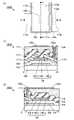
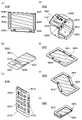
<1-1.半導体装置の構成例1>
図1(A)は、本発明の一態様の半導体装置であるトランジスタ100Aの上面図であり、図1(B)は、図1(A)に示す一点鎖線X1-X2間における切断面の断面図に相当し、図1(C)は、図1(A)に示す一点鎖線Y1-Y2間における切断面の断面図に相当する。なお、図1(A)において、煩雑になることを避けるため、トランジスタ100Aの構成要素の一部(ゲート絶縁膜として機能する絶縁膜等)を省略して図示している。また、一点鎖線X1-X2方向をチャネル長方向、一点鎖線Y1-Y2方向をチャネル幅方向と呼称する場合がある。なお、トランジスタの上面図においては、以降の図面においても図1(A)と同様に、構成要素の一部を省略して図示する場合がある。<1-1. Configuration Example 1 of Semiconductor Device>
FIG. 1A is a top view of a
トランジスタ100Aは、基板102上の導電膜104と、基板102及び導電膜104上の絶縁膜106と、絶縁膜106上の金属酸化物108と、金属酸化物108上の導電膜112aと、金属酸化物108上の導電膜112bと、を有する。また、トランジスタ100A上、具体的には、金属酸化物108、導電膜112a、及び導電膜112b上には、絶縁膜115が形成されている。The
なお、トランジスタ100Aは、所謂チャネルエッチ型のトランジスタである。Note that the
また、絶縁膜115は、シリコンと、窒素及び酸素のいずれか一方または双方と、を有すると好ましい。Further, the insulating
絶縁膜115は過剰な酸素を有し、金属酸化物108に酸素を供給することができる。The insulating
また、金属酸化物108は、絶縁膜106上の金属酸化物108_1と、金属酸化物108_1の上面に接する金属酸化物108_2と、を有する。In addition, the
なお、金属酸化物108_1、及び金属酸化物108_2は、それぞれ、Inと、元素M(Mは、ガリウム、アルミニウム、シリコン、ホウ素、イットリウム、スズ、銅、バナジウム、ベリリウム、チタン、鉄、ニッケル、ゲルマニウム、ジルコニウム、モリブデン、ランタン、セリウム、ネオジム、ハフニウム、タンタル、タングステン、またはマグネシウム)と、Znと、を有する。特に、元素Mとしてはガリウムが好ましい。Note that the metal oxide 108_1 and the metal oxide 108_2 are respectively In and an element M (M is gallium, aluminum, silicon, boron, yttrium, tin, copper, vanadium, beryllium, titanium, iron, nickel, germanium , zirconium, molybdenum, lanthanum, cerium, neodymium, hafnium, tantalum, tungsten, or magnesium) and Zn. Gallium is particularly preferable as the element M.
なお、図1(A)(B)(C)に示すトランジスタ100Aにおいて、絶縁膜106は、トランジスタ100Aのゲート絶縁膜としての機能を有し、絶縁膜115は、トランジスタ100Aの保護絶縁膜としての機能を有する。また、トランジスタ100Aにおいて、導電膜104は、ゲート電極としての機能を有し、導電膜112aは、ソース電極としての機能を有し、導電膜112bは、ドレイン電極としての機能を有する。なお、本明細書等において、絶縁膜106を第1の絶縁膜と、絶縁膜115を第2の絶縁膜と、それぞれ呼称する場合がある。Note that in the
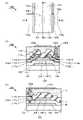
図2(A)は、トランジスタ100Aの、金属酸化物108と、導電膜112aと、導電膜112bと、のみを示した上面図である。上面から見ると、導電膜112aと、導電膜112bとは、金属酸化物108より手前に配置される。金属酸化物108のうち、導電膜112aと接する領域をソース領域、導電膜112bと接する領域をドレイン領域、と言うことができる。尚、上記ソース領域とドレイン領域とは入れ替えて定めてもよい。FIG. 2A is a top view showing only the
上面から見たとき、導電膜112aと、導電膜112bと、のチャネル長方向の間隔は、間隔206と、間隔207と、の2種類に分けられる。金属酸化物108が形成され、かつ導電膜112aと、導電膜112bと、の間にあり、かつ導電膜112aと、導電膜112bとの間隔が間隔206である領域は、チャネル形成領域201であり、同じく間隔207である領域は、端部領域202Aまたは端部領域202Bである。When viewed from the top, the distance between the
端部領域202Aまたは端部領域202Bは、それぞれ金属酸化物108の端部204A、端部204B、を有する。端部204A及び端部204Bは隣接する層から元素が拡散する場合や、不安定な結合を有する場合があるため、端部領域202Aまたは端部領域202Bは、チャネル形成領域201より高い導電率σを有する可能性がある。または、端部領域202Aまたは端部領域202Bに、トランジスタ特性に影響のあるトラップ準位が形成される可能性がある。尚、端部領域202A、端部領域202B及びチャネル形成領域201は、ソース領域と、ドレイン領域と、にチャネル長方向に沿って挟まれる。
チャネル形成領域201の、チャネル幅方向の長さは、チャネル幅211であり、端部領域202Aまたは端部領域202Bの、チャネル幅方向の長さは、端部幅212である。端部幅212は0より大であり、金属酸化物108のチャネル幅方向の長さの半分より小である。The length of the
端部領域202Aまたは端部領域202Bは、金属酸化物108の端部を含んでいる。導電膜112a又は導電膜112bと、金属酸化物108とが重ならない領域において、チャネル形成領域201より高い導電率σを有する金属酸化物108の領域の全てが、端部領域202A又は端部領域202Bに含まれることが好ましい。つまり、端部領域202Aまたは端部領域202Bに、チャネル形成領域201より高い導電率σを有する金属酸化物がすべて含まれる端部幅212を選ぶことが好ましい。または、トランジスタ特性に影響のあるトラップ準位が形成された端部付近の金属酸化物がすべて含まれる端部幅212を選ぶことが好ましい。好ましい端部幅212の大きさは、プロセス条件により異なる。例えばプロセス上限温度が高い場合は、端部幅212は大きい。
端部領域202Aまたは端部領域202Bはトランジスタ特性への影響が小であるとして、トランジスタ特性は、チャネル幅211にて計算することができる。The transistor characteristics can be calculated with the
間隔207が小さくなると、導電膜112aと、端部領域202Aまたは端部領域202Bと、導電膜112bと、の直列抵抗が小さくなり、トランジスタ特性への影響が顕著である。As the
そこで、間隔206が0μmより大であり4μm未満、好ましくは0μmより大であり2.5μm未満、であるトランジスタにおいては、以下の間隔207とする。すなわち間隔207は間隔206より大であり、金属酸化物108のチャネル長方向の長さより小とする。好ましくは間隔207は間隔206の3倍より大であり、金属酸化物108のチャネル長方向の長さより小とする。Therefore, in a transistor where the
間隔207を間隔206より大とすることで、導電膜112aと、端部領域202Aまたは端部領域202Bと、導電膜112bと、の直列抵抗が大きくなり、ばらつきの少ないトランジスタ特性を有する金属酸化物を用いた半導体装置を提供することができる。また、優れたノーマリオフのスイッチング特性を有する金属酸化物を用いた半導体装置を提供することができる。When the
また本発明の一態様のトランジスタは、金属酸化物108の端部を有し、導電膜112aまたは導電膜112bと重なる、領域203A、203B、203C、203D、を有する。The transistor of one embodiment of the present invention also includes
領域203A、203B、203C、203D、を有することで、金属酸化物108と、導電膜112aまたは導電膜112bとの接触抵抗を下げることができる。また、トランジスタを表示装置に用いたとき、領域203A、203B、203C、203D、を有することで、膜面と平行な方向に沿ってチャネル形成領域201に到達する迷光を低減することができる。By having the
また半導体装置の有する層間膜の材料や、プロセスの熱処理条件、使用環境によっては、水素のチャネル形成領域201方向への拡散量が大きいことがある。導電膜112aと、導電膜112bとが、チャネル形成領域201及びその周辺の水素を吸収する効果がある場合、トランジスタの導電率σが高くなるのを防ぐことができる。より大きな面積で導電膜112aと、導電膜112bとを形成したい場合に、トランジスタが領域203A、203B、203C、203Dを有することは有効である。In addition, depending on the material of the interlayer film of the semiconductor device, the heat treatment conditions of the process, and the usage environment, the amount of diffusion of hydrogen toward the
チャネル形成領域201及びその周辺の水素を吸収する効果がある導電膜112aと、導電膜112bと、の材料の例としては、導電性を有する酸化物、例えば、インジウム錫酸化物、酸化タングステンを含むインジウム酸化物、酸化タングステンを含むインジウム亜鉛酸化物、酸化チタンを含むインジウム酸化物、酸化チタンを含むインジウム錫酸化物、インジウム亜鉛酸化物、シリコンを添加したインジウム錫酸化物、または窒素を含むインジウムガリウム亜鉛酸化物を成膜し、該酸化物上に、アルミニウム、クロム、銅、銀、金、白金、タンタル、ニッケル、チタン、モリブデン、タングステン、ハフニウム、バナジウム、ニオブ、マンガン、マグネシウム、ジルコニウム、ベリリウム、インジウムなどから選ばれた金属元素を1種以上含む材料、または、リン等の不純物元素を含有させた多結晶シリコンに代表される、電気伝導度が高い半導体、ニッケルシリサイドなどのシリサイドを成膜してもよい。または、該酸化物の代わりにチタンを用いても同様の機能を有する場合がある。Examples of the material of the
またチャネル長方向に沿って、チャネル形成領域201は、領域203Aと、領域203Bとの間に位置する。同様にチャネル長方向に沿って、チャネル形成領域201は、領域203Cと、領域203Dとの間に位置する。この配置により、導電膜112aと、導電膜112bとの最短距離は、チャネル長である間隔206となる。換言すれば、ソース領域から、ドレイン領域への最短経路は、チャネル形成領域201に含まれる。Along the channel length direction, the
端部領域202Aと領域203Aとの境界は、チャネル幅方向に対して平行でなくても良い。例えば、金属酸化物108の端部から離れるに従って、導電膜112aと、導電膜112bとの間隔が小さくなる形状でも良い(図2(B)参照)。この形状の配置は、金属酸化物における端部の影響が小さく、なるべく端部幅212を小さくしたいものの、露光やエッチングによる微細化の限界にある場合に有効である。The boundary between the
<1-2.半導体装置の構成要素>
次に、本実施の形態の半導体装置に含まれる構成要素について、詳細に説明する。<1-2. Components of Semiconductor Device>
Next, the components included in the semiconductor device of this embodiment will be described in detail.
[基板]
基板102の材質などに大きな制限はないが、少なくとも、後の熱処理に耐えうる程度の耐熱性を有している必要がある。例えば、ガラス基板、セラミック基板、石英基板、サファイア基板等を、基板102として用いてもよい。また、シリコンや炭化シリコンを材料とした単結晶半導体基板、多結晶半導体基板、シリコンゲルマニウム等の化合物半導体基板、SOI基板等を適用することも可能であり、これらの基板上に半導体素子が設けられたものを、基板102として用いてもよい。なお、基板102として、ガラス基板を用いる場合、第6世代(1500mm×1850mm)、第7世代(1870mm×2200mm)、第8世代(2200mm×2400mm)、第9世代(2400mm×2800mm)、第10世代(2950mm×3400mm)等の大面積基板を用いることで、大型の表示装置を作製することができる。[substrate]
There are no particular restrictions on the material of the
また、基板102として、可撓性基板を用い、可撓性基板上に直接、トランジスタ100Aを形成してもよい。または、基板102とトランジスタ100Aとの間に剥離層を設けてもよい。剥離層は、その上に半導体装置を一部あるいは全部完成させた後、基板102より分離し、他の基板に転載するのに用いることができる。その際、トランジスタ100Aは耐熱性の劣る基板や可撓性の基板にも転載できる。Alternatively, a flexible substrate may be used as the
[導電膜]
ゲート電極として機能する導電膜104、ソース電極として機能する導電膜112a、及びドレイン電極として機能する導電膜112bとしては、クロム(Cr)、銅(Cu)、アルミニウム(Al)、金(Au)、銀(Ag)、亜鉛(Zn)、モリブデン(Mo)、タンタル(Ta)、チタン(Ti)、タングステン(W)、マンガン(Mn)、ニッケル(Ni)、鉄(Fe)、コバルト(Co)から選ばれた金属元素、または上述した金属元素を成分とする合金か、上述した金属元素を組み合わせた合金等を用いてそれぞれ形成することができる。[Conductive film]
As the
また、導電膜104、112a、112bには、インジウムと錫とを有する酸化物(In-Sn酸化物)、インジウムとタングステンとを有する酸化物(In-W酸化物)、インジウムとタングステンと亜鉛とを有する酸化物(In-W-Zn酸化物)、インジウムとチタンとを有する酸化物(In-Ti酸化物)、インジウムとチタンと錫とを有する酸化物(In-Ti-Sn酸化物)、インジウムと亜鉛とを有する酸化物(In-Zn酸化物)、インジウムと錫とシリコンとを有する酸化物(In-Sn-Si酸化物)、インジウムとガリウムと亜鉛とを有する酸化物(In-Ga-Zn酸化物)等の酸化物導電体または酸化物半導体を適用することもできる。In the
ここで、酸化物導電体について説明を行う。本明細書等において、酸化物導電体をOC(Oxide Conductor)と呼称してもよい。酸化物導電体としては、例えば、酸化物半導体に酸素欠損を形成し、該酸素欠損に水素を添加すると、伝導帯近傍にドナー準位が形成される。この結果、酸化物半導体は、導電性が高くなり導電体化する。導電体化された酸化物半導体を、酸化物導電体ということができる。一般に、酸化物半導体は、エネルギーギャップが大きいため、可視光に対して透光性を有する。一方、酸化物導電体は、伝導帯近傍にドナー準位を有する酸化物半導体である。したがって、酸化物導電体は、ドナー準位による吸収の影響は小さく、可視光に対して酸化物半導体と同程度の透光性を有する。Here, the oxide conductor will be described. In this specification and the like, an oxide conductor may be referred to as an OC (Oxide Conductor). As an oxide conductor, for example, oxygen vacancies are formed in an oxide semiconductor, and when hydrogen is added to the oxygen vacancies, a donor level is formed near the conduction band. As a result, the oxide semiconductor has high conductivity and becomes a conductor. A conductive oxide semiconductor can be referred to as an oxide conductor. In general, an oxide semiconductor has a large energy gap and thus has a property of transmitting visible light. On the other hand, an oxide conductor is an oxide semiconductor having a donor level near the conduction band. Therefore, an oxide conductor is less affected by absorption due to a donor level and has a visible light-transmitting property similar to that of an oxide semiconductor.
また、導電膜104、112a、112bには、Cu-X合金膜(Xは、Mn、Ni、Cr、Fe、Co、Mo、Ta、またはTi)を適用してもよい。Cu-X合金膜を用いることで、ウエットエッチングプロセスで加工できるため、製造コストを抑制することが可能となる。A Cu—X alloy film (where X is Mn, Ni, Cr, Fe, Co, Mo, Ta, or Ti) may be applied to the
また、導電膜112a、112bには、上述の金属元素の中でも、特に銅、チタン、タングステン、タンタル、及びモリブデンの中から選ばれるいずれか一つまたは複数を有すると好適である。特に、導電膜112a、112bとしては、窒化タンタル膜を用いると好適である。当該窒化タンタル膜は、導電性を有し、且つ、銅または水素に対して、高いバリア性を有する。また、窒化タンタル膜は、さらに自身からの水素の放出が少ないため、金属酸化物108と接する導電膜、または金属酸化物108の近傍の導電膜として、最も好適に用いることができる。また、導電膜112a、112bとして、銅膜を用いると、導電膜112a、112bの抵抗を低くすることができるため好適である。In addition, it is preferable that the
また、導電膜112a、112bを、無電解めっき法により形成することができる。当該無電解めっき法により形成できる材料としては、例えば、Cu、Ni、Al、Au、Sn、Co、Ag、及びPdの中から選ばれるいずれか一つまたは複数を用いることが可能である。特に、CuまたはAgを用いると、導電膜の抵抗を低くすることができるため、好適である。Alternatively, the
[ゲート絶縁膜として機能する絶縁膜]
トランジスタ100Aのゲート絶縁膜として機能する絶縁膜106としては、プラズマ化学気相堆積(PECVD:(Plasma Enhanced Chemical Vapor Deposition))法、スパッタリング法等により、酸化シリコン膜、酸化窒化シリコン膜、窒化酸化シリコン膜、窒化シリコン膜、酸化アルミニウム膜、酸化ハフニウム膜、酸化イットリウム膜、酸化ジルコニウム膜、酸化ガリウム膜、酸化タンタル膜、酸化マグネシウム膜、酸化ランタン膜、酸化セリウム膜および酸化ネオジム膜を一種以上含む絶縁層を用いることができる。なお、絶縁膜106を、積層構造、または3層以上の積層構造としてもよい。[Insulating film functioning as gate insulating film]
As the insulating
また、トランジスタ100Aのチャネル形成領域として機能する金属酸化物108と接する絶縁膜106は、酸化物絶縁膜であることが好ましく、化学量論的組成よりも過剰に酸素を含有する領域(過剰酸素領域)を有することがより好ましい。Insulating
ただし、上記構成に限定されず、金属酸化物108と接する絶縁膜に、窒化物絶縁膜を用いる構成としてもよい。当該構成の一例としては、窒化シリコン膜を形成し、当該窒化シリコン膜の表面に酸素プラズマ処理などを行うことで、窒化シリコン膜の表面を酸化させる構成などが挙げられる。なお、窒化シリコン膜の表面に酸素プラズマ処理などを行った場合、窒化シリコン膜の表面は原子レベルで酸化されている場合があるため、トランジスタの断面の観察等を行っても、酸素が検出されない可能性がある。すなわち、トランジスタの断面の観察を行った場合、窒化シリコン膜と、金属酸化物とが、接しているように観察される場合がある。However, the structure is not limited to the above structure, and a structure using a nitride insulating film as an insulating film in contact with the
なお、窒化シリコン膜は、酸化シリコン膜と比較して比誘電率が高く、酸化シリコン膜と同等の静電容量を得るのに必要な膜厚が大きいため、トランジスタのゲート絶縁膜として、窒化シリコン膜を含むことで絶縁膜を厚膜化することができる。よって、トランジスタの絶縁耐圧の低下を抑制、さらには絶縁耐圧を向上させて、トランジスタの静電破壊を抑制することができる。Note that a silicon nitride film has a higher relative dielectric constant than a silicon oxide film and has a large film thickness necessary to obtain a capacitance equivalent to that of a silicon oxide film. By including the film, the insulating film can be thickened. Therefore, a decrease in the dielectric strength voltage of the transistor can be suppressed, and furthermore, the dielectric strength voltage can be improved, and electrostatic breakdown of the transistor can be suppressed.
[金属酸化物]
金属酸化物108としては、先に示す材料を用いることができる。金属酸化物108_1及び金属酸化物108_2は、それぞれIn、M、及びZnの原子数の総和に対して、Inの含有量が40%以上50%以下の領域と、Mの含有量が5%以上30%以下の領域と、を有する。金属酸化物108_1及び金属酸化物108_2が、それぞれ上記の領域を有することで、キャリア密度を高めることができる。[Metal oxide]
As the
具体的には、金属酸化物108_1及び金属酸化物108_2のIn、M、及びZnの原子数の比を、それぞれIn:M:Zn=4:2:3近傍、またはIn:M:Zn=5:1:6近傍とすると好ましい。ここで、4:2:3近傍とは、In、M、及びZnの原子数の総和に対して、Inが4の場合、Mが1.5以上2.5以下であり、且つZnが2以上4以下である。また、5:1:6近傍とは、In、M、及びZnの原子数の総和に対して、Inが5の場合、Mが0.5以上1.5以下であり、且つZnが5以上7以下である。Specifically, the ratio of the number of atoms of In, M, and Zn in the metal oxide 108_1 and the metal oxide 108_2 is approximately In:M:Zn=4:2:3, or In:M:Zn=5. : It is preferable to make it near 1:6. Here, near 4:2:3 means that, with respect to the total number of atoms of In, M, and Zn, when In is 4, M is 1.5 or more and 2.5 or less, and Zn is 2 4 or less. Further, near 5:1:6 means that, with respect to the total number of atoms of In, M, and Zn, when In is 5, M is 0.5 or more and 1.5 or less, and Zn is 5 or more. 7 or less.
また、金属酸化物108_1は、金属酸化物108_2よりも結晶性が低い領域を有すると好ましい。金属酸化物108_1が、金属酸化物108_2よりも結晶性が低い領域を有することで、キャリア密度を高め、且つ信頼性の高い半導体装置とすることができる。例えば、トランジスタ100Aは、チャネルエッチ型のトランジスタであるため、金属酸化物108_1よりも金属酸化物108_2の結晶性を高めることで、金属酸化物108_2が金属酸化物108_1のエッチングストッパとして機能する。Further, the metal oxide 108_1 preferably has a region with lower crystallinity than the metal oxide 108_2. When the metal oxide 108_1 has a region with lower crystallinity than the metal oxide 108_2, the carrier density can be increased and the semiconductor device can have high reliability. For example, since the
また、金属酸化物108_2のIn、M、及びZnの原子数の比を上記範囲とすることで、金属酸化物108_2と、導電膜112a、112bとの接触抵抗を低くすることができる。Further, when the ratio of the number of atoms of In, M, and Zn in the metal oxide 108_2 is within the above range, contact resistance between the metal oxide 108_2 and the
なお、金属酸化物108を上記構成とすることでトランジスタ100Aの電界効果移動度を高くすることができる。具体的には、トランジスタ100Aの電界効果移動度が50cm2/Vsを超える、さらに好ましくはトランジスタ100Aの電界効果移動度が100cm2/Vsを超えることが可能となる。Note that the field-effect mobility of the
例えば、上記の電界効果移動度が高いトランジスタを、ゲート信号を生成するゲートドライバに用いることで、額縁幅の狭い(狭額縁ともいう)表示装置を提供することができる。また、上記の電界効果移動度が高いトランジスタを、表示装置が有する信号線からの信号の供給を行うソースドライバ(とくに、ソースドライバが有するシフトレジスタの出力端子に接続されるデマルチプレクサ)に用いることで、表示装置に接続される配線数が少ない表示装置を提供することができる。For example, by using the above transistor with high field-effect mobility for a gate driver that generates a gate signal, a display device with a narrow frame width (also referred to as a narrow frame) can be provided. Further, the above transistor with high field-effect mobility is used for a source driver that supplies a signal from a signal line included in a display device (in particular, a demultiplexer connected to an output terminal of a shift register included in the source driver). Therefore, a display device with a small number of wirings connected to the display device can be provided.
なお、金属酸化物108_1及び金属酸化物108_2の結晶構造は、特に限定されない。金属酸化物108_1及び金属酸化物108_2は、それぞれ単結晶構造または非単結晶構造のいずれか一方または双方でもよい。Note that the crystal structures of the metal oxide 108_1 and the metal oxide 108_2 are not particularly limited. Each of the metal oxide 108_1 and the metal oxide 108_2 may have either or both of a single crystal structure and a non-single crystal structure.
非単結晶構造は、例えば、後述するCAAC-OS(C Axis Aligned Crystalline Oxide Semiconductor)、多結晶構造、微結晶構造、及び非晶質構造を含む。また、結晶構造としては、ビックスバイト型の結晶構造、層状の結晶構造などが挙げられる。また、ビックスバイト型の結晶構造と、層状の結晶構造との双方を含む混晶構造としてもよい。The non-single-crystal structure includes, for example, a CAAC-OS (C Axis Aligned Crystalline Oxide Semiconductor), a polycrystalline structure, a microcrystalline structure, and an amorphous structure, which will be described later. In addition, examples of the crystal structure include a bixbyite crystal structure and a layered crystal structure. Alternatively, a mixed crystal structure including both a bixbyite crystal structure and a layered crystal structure may be used.
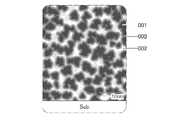
また、金属酸化物108_2は、層状の結晶構造、特にc軸配向性を有する結晶構造を有すると好適である。別言すると、金属酸化物108_2は、CAAC-OSであると好適である。The metal oxide 108_2 preferably has a layered crystal structure, particularly a crystal structure with c-axis orientation. In other words, the metal oxide 108_2 is preferably CAAC-OS.
例えば、金属酸化物108_1を、微結晶構造とし、金属酸化物108_2を、c軸配向性を有する結晶構造とすると好適である。別言すると、金属酸化物108_1は、金属酸化物108_2よりも結晶性が低い領域を有する。なお、金属酸化物108の結晶性としては、例えば、X線回折(XRD:X-Ray Diffraction)を用いて分析する、あるいは、透過型電子顕微鏡(TEM:Transmission Electron Microscope)を用いて分析することで解析できる。For example, it is preferable that the metal oxide 108_1 has a microcrystalline structure and the metal oxide 108_2 has a crystal structure with c-axis orientation. In other words, the metal oxide 108_1 has regions with lower crystallinity than the metal oxide 108_2. The crystallinity of the
例えば、金属酸化物108をXRD分析により測定した場合に、金属酸化物108_1は、2θ=31°近傍にピークが観察され難く、金属酸化物108_2は、2θ=31°近傍にピークが観察される。For example, when the
金属酸化物108_1が結晶性の低い領域を有する場合、以下の優れた効果を有する。When the metal oxide 108_1 has a region with low crystallinity, it has the following excellent effects.
まず、金属酸化物108_1中に形成されうる酸素欠損について説明を行う。First, oxygen vacancies that can be formed in the metal oxide 108_1 are described.
金属酸化物108_1に形成される酸素欠損は、トランジスタ特性に影響を与えるため問題となる。例えば、金属酸化物108_1中に酸素欠損が形成されると、該酸素欠損に水素が結合し、キャリア供給源となる。金属酸化物108_1中にキャリア供給源が生成されると、金属酸化物108_1を有するトランジスタ100Aの電気特性の変動、代表的にはしきい値電圧のシフトが生じる。したがって、金属酸化物108_1においては、酸素欠損が少ないほど好ましい。Oxygen vacancies formed in the metal oxide 108_1 pose a problem because they affect transistor characteristics. For example, when oxygen vacancies are formed in the metal oxide 108_1, hydrogen bonds to the oxygen vacancies and serves as a carrier supply source. The generation of a carrier source in metal oxide 108_1 causes variations in the electrical characteristics of
そこで、本発明の一態様においては、金属酸化物108_1上に金属酸化物108_2が形成される。金属酸化物108_2は、金属酸化物108_1よりも酸素を多く含有する構成である。金属酸化物108_2の形成時または、金属酸化物108_2の形成後に、金属酸化物108_2から金属酸化物108_1に酸素または過剰酸素が移動することで、金属酸化物108_1中の酸素欠損を低減することが可能となる。Therefore, in one embodiment of the present invention, metal oxide 108_2 is formed over metal oxide 108_1. The metal oxide 108_2 contains more oxygen than the metal oxide 108_1. When the metal oxide 108_2 is formed or after the metal oxide 108_2 is formed, oxygen or excess oxygen moves from the metal oxide 108_2 to the metal oxide 108_1, whereby oxygen vacancies in the metal oxide 108_1 can be reduced. It becomes possible.
また、金属酸化物108_2の形成時に、酸素を多く含む雰囲気とすることで、金属酸化物108_2の結晶性を高めることができる。Further, when the metal oxide 108_2 is formed in an atmosphere containing a large amount of oxygen, the crystallinity of the metal oxide 108_2 can be improved.
金属酸化物108_2の結晶性を高めることで、金属酸化物108_1に混入しうる不純物を抑制することができる。特に、金属酸化物108_2の結晶性を高めることで、導電膜112a、112bを加工する際に、金属酸化物108_1へのダメージを抑制することができる。金属酸化物108の表面、すなわち金属酸化物108_2の表面は、導電膜112a、112bの加工の際のエッチャントまたはエッチングガスに曝される。しかしながら、金属酸化物108_2は、結晶性が高い領域を有するため、結晶性が低い金属酸化物108_1と比較してエッチング耐性に優れる。したがって、金属酸化物108_2は、エッチングストッパとして機能する。By increasing the crystallinity of the metal oxide 108_2, impurities that can enter the metal oxide 108_1 can be suppressed. In particular, by increasing the crystallinity of the metal oxide 108_2, damage to the metal oxide 108_1 can be suppressed when the
なお、金属酸化物108としては、不純物濃度が低く、欠陥準位密度の低い金属酸化物を用いることで、優れた電気特性を有するトランジスタを作製することができ好ましい。ここでは、不純物濃度が低く、欠陥準位密度の低い(酸素欠損の少ない)ことを高純度真性または実質的に高純度真性とよぶ。なお、金属酸化物中の不純物としては、代表的には水、水素などが挙げられる。また、本明細書等において、金属酸化物中から水及び水素を低減または除去することを、脱水化、脱水素化と表す場合がある。また、金属酸化物に酸素を添加することを、加酸素化と表す場合があり、加酸素化され且つ化学量論的組成よりも過剰の酸素を有する状態を過酸素化状態と表す場合がある。Note that a metal oxide with a low impurity concentration and a low defect level density is preferably used as the
高純度真性または実質的に高純度真性である金属酸化物は、キャリア発生源が少ないため、キャリア密度を低くすることができる。従って、該金属酸化物にチャネル形成領域が形成されるトランジスタは、しきい値電圧がマイナスとなる電気特性(ノーマリオンともいう。)になることが少ない。また、高純度真性または実質的に高純度真性である金属酸化物は、欠陥準位密度が低いため、トラップ準位密度も低くなる場合がある。また、高純度真性または実質的に高純度真性である金属酸化物は、オフ電流が著しく小さく、チャネル幅が1×106μmでチャネル長Lが10μmの素子であっても、ソース電極とドレイン電極間の電圧(ドレイン電圧)が1Vから10Vの範囲において、オフ電流が、半導体パラメータアナライザの測定限界以下、すなわち1×10-13A以下という特性を得ることができる。High-purity intrinsic or substantially high-purity intrinsic metal oxides have few carrier generation sources, and thus can have a low carrier density. Therefore, a transistor in which a channel formation region is formed in the metal oxide rarely has electrical characteristics in which the threshold voltage is negative (also referred to as normally on). In addition, since a highly pure intrinsic or substantially highly pure intrinsic metal oxide has a low defect level density, the trap level density may also be low. In addition, a highly purified intrinsic or substantially highly purified intrinsic metal oxide has a remarkably small off current, and even in a device having a channel width of 1×106 μm and a channel length L of 10 μm, the source electrode and the drain When the voltage between the electrodes (drain voltage) is in the range of 1 V to 10 V, the characteristic that the off current is below the measurement limit of the semiconductor parameter analyzer, that is, below 1×10⁻¹³ A can be obtained.
また、金属酸化物108_1は、金属酸化物108_2よりも結晶性が低い領域を有することで、キャリア密度が高くなる場合がある。金属酸化物108_1のキャリア密度が高くなると、金属酸化物108_1の伝導帯に対してフェルミ準位が相対的に高くなる場合がある。これにより、金属酸化物108_1の伝導帯の下端が低くなり、金属酸化物108_1の伝導帯下端と、ゲート絶縁膜(ここでは、絶縁膜106)中に形成されうるトラップ準位とのエネルギー差が大きくなる場合がある。該エネルギー差が大きくなることにより、ゲート絶縁膜中にトラップされる電荷が少なくなり、トランジスタのしきい値電圧の変動を小さくできる場合がある。また、金属酸化物108_1のキャリア密度が高くなると、金属酸化物108の電界効果移動度を高めることができる。Further, since the metal oxide 108_1 has a region with lower crystallinity than the metal oxide 108_2, the carrier density may be high. When the carrier density of the metal oxide 108_1 increases, the Fermi level may become relatively high with respect to the conduction band of the metal oxide 108_1. As a result, the bottom of the conduction band of the metal oxide 108_1 is lowered, and the energy difference between the bottom of the conduction band of the metal oxide 108_1 and the trap level that can be formed in the gate insulating film (here, the insulating film 106) is increased. It may grow. By increasing the energy difference, the amount of charge trapped in the gate insulating film is reduced, and fluctuations in the threshold voltage of the transistor can be reduced in some cases. Further, when the carrier density of the metal oxide 108_1 is increased, the field effect mobility of the
金属酸化物108_1及び金属酸化物108_2が、それぞれIn-M-Zn酸化物の場合、In-M-Zn酸化物を成膜するために用いるスパッタリングターゲットの金属元素の原子数比は、In>Mを満たすことが好ましい。このようなスパッタリングターゲットの金属元素の原子数比として、In:M:Zn=2:1:3、In:M:Zn=3:1:2、In:M:Zn=4:2:4.1、In:M:Zn=5:1:6、In:M:Zn=5:1:7、In:M:Zn=5:1:8、In:M:Zn=6:1:6、In:M:Zn=5:2:5等が挙げられる。When each of the metal oxide 108_1 and the metal oxide 108_2 is an In-M-Zn oxide, the atomic ratio of the metal elements in the sputtering target used for forming the In-M-Zn oxide is In>M. is preferably satisfied. The atomic ratios of metal elements in such a sputtering target are In:M:Zn=2:1:3, In:M:Zn=3:1:2, In:M:Zn=4:2:4. 1, In:M:Zn=5:1:6, In:M:Zn=5:1:7, In:M:Zn=5:1:8, In:M:Zn=6:1:6, In:M:Zn=5:2:5 and the like.
なお、成膜される金属酸化物108_1及び金属酸化物108_2の原子数比は、それぞれ上記のスパッタリングターゲットに含まれる金属元素の原子数比のプラスマイナス40%の変動を含む。例えば、金属酸化物108_1及び金属酸化物108_2に用いるスパッタリングターゲットの組成が、In:Ga:Zn=4:2:4.1[原子数比]の場合、成膜される金属酸化物108_1及び金属酸化物108_2の組成は、それぞれIn:Ga:Zn=4:2:3[原子数比]の近傍となる場合がある。Note that the atomic ratios of the metal oxide 108_1 and the metal oxide 108_2 to be formed include variations of plus or minus 40% of the atomic ratio of the metal elements contained in the above sputtering targets. For example, when the composition of the sputtering target used for the metal oxide 108_1 and the metal oxide 108_2 is In:Ga:Zn=4:2:4.1 [atomic ratio], the metal oxide 108_1 and the metal The composition of the oxide 108_2 may be in the vicinity of In:Ga:Zn=4:2:3 [atomic ratio].
また、金属酸化物108_1及び金属酸化物108_2は、それぞれエネルギーギャップが2.5eV以上、好ましくは3.0eV以上である。このように、エネルギーギャップの広い金属酸化物を用いることで、トランジスタ100Aのオフ電流を低減することができる。The metal oxide 108_1 and the metal oxide 108_2 each have an energy gap of 2.5 eV or more, preferably 3.0 eV or more. By using a metal oxide with a wide energy gap in this manner, off-state current of the
[保護絶縁膜として機能する絶縁膜]
絶縁膜115は、トランジスタ100Aの保護絶縁膜としての機能を有する。または、絶縁膜115は、金属酸化物108に酸素を供給する機能を有する。[Insulating film functioning as a protective insulating film]
The insulating
例えば、絶縁膜115としては、シリコンと、窒素及び酸素のいずれか一方または双方とを有すると好ましい。また、絶縁膜115としては、シリコンと、酸素と、を含む第1の層と、シリコンと、窒素と、を含む第2の層と、を有すると好ましい。For example, the insulating
また、絶縁膜115は、窒素酸化物(NOx、xは0よりも大きく2以下、好ましくは1以上2以下、代表的にはNOまたはNO2)に起因する準位密度が低い絶縁膜を用いると好ましい。Further, the insulating
窒素酸化物は、絶縁膜115などに準位を形成する。当該準位は、金属酸化物108のエネルギーギャップ内に位置する。例えば、当該窒素酸化物に起因する準位密度は、金属酸化物108の価電子帯の上端のエネルギー(Ev_os)と、金属酸化物108の伝導帯の下端のエネルギー(Ec_os)との間に形成され得る場合がある。そのため、窒素酸化物が、絶縁膜115及び金属酸化物108の界面に拡散すると、当該準位が絶縁膜115側において電子をトラップする場合がある。この結果、トラップされた電子が、絶縁膜115及び金属酸化物108界面近傍に留まるため、トランジスタのしきい値電圧をプラス方向にシフトさせてしまう。Nitrogen oxide forms a level in the insulating
絶縁膜115として、窒素酸化物に起因する準位密度が低い絶縁膜とすることで、トランジスタのしきい値電圧のシフトを低減することが可能であり、トランジスタの電気特性の変動を低減することができる。By using an insulating film with a low level density due to nitrogen oxide as the insulating
なお、上記記載の、導電膜、絶縁膜、金属酸化物などの様々な膜としては、スパッタリング法やPECVD法により形成することができるが、他の方法、例えば、熱CVD(Chemical Vapor Deposition)法により形成してもよい。熱CVD法の例としてMOCVD(Metal Organic Chemical Vapor Deposition)法、またはALD(Atomic Layer Deposition)法などが挙げられる。Various films such as the conductive film, the insulating film, and the metal oxide described above can be formed by a sputtering method or a PECVD method, but other methods such as a thermal CVD (Chemical Vapor Deposition) method can be used. may be formed by Examples of thermal CVD include MOCVD (Metal Organic Chemical Vapor Deposition) and ALD (Atomic Layer Deposition).
熱CVD法は、プラズマを使わない成膜方法のため、プラズマダメージにより欠陥が生成されることが無いという利点を有する。また、熱CVD法としては、原料ガスをチャンバー内に送り、チャンバー内を大気圧または減圧下とし、基板上に膜を堆積させればよい。The thermal CVD method is a film forming method that does not use plasma, so it has the advantage of not generating defects due to plasma damage. As for the thermal CVD method, a source gas is sent into a chamber, the chamber is made to be under atmospheric pressure or reduced pressure, and a film is deposited on the substrate.
また、ALD法としては、原料ガスをチャンバー内に送り、チャンバー内を大気圧または減圧下とし、基板上に膜を堆積させればよい。In the ALD method, a source gas is fed into a chamber, the chamber is made to be under atmospheric pressure or reduced pressure, and a film is deposited on the substrate.
<1-3.半導体装置の構成例2>
次に、図1(A)(B)(C)に示すトランジスタ100Aの変形例について、図3を用いて説明する。<1-3. Configuration Example 2 of Semiconductor Device>
Next, a modification example of the
また、図3(A)は、本発明の一態様の半導体装置であるトランジスタ100Bの上面図であり、図3(B)は、図3(A)に示す一点鎖線X1-X2間における切断面の断面図に相当し、図3(C)は、図3(A)に示す一点鎖線Y1-Y2間における切断面の断面図に相当する。3A is a top view of a
トランジスタ100Bは、基板102上の導電膜104と、基板102及び導電膜104上の絶縁膜106と、絶縁膜106上の金属酸化物108と、金属酸化物108上の導電膜112aと、金属酸化物108上の導電膜112bと、金属酸化物108、導電膜112a、及び導電膜112b上の絶縁膜115と、絶縁膜115上の絶縁膜116と、絶縁膜116上の導電膜120aと、絶縁膜116上の導電膜120bと、を有する。The
また、絶縁膜106は、開口部151を有し、絶縁膜106上には、開口部151を介して導電膜104と電気的に接続される導電膜112cが形成される。また、絶縁膜115及び絶縁膜116は、導電膜112bに達する開口部152aと、導電膜112cに達する開口部152bとを有する。The insulating
なお、トランジスタ100Bにおいて、絶縁膜106は、トランジスタ100Bの第1のゲート絶縁膜としての機能を有し、絶縁膜115、116は、トランジスタ100Bの第2のゲート絶縁膜としての機能を有する。また、トランジスタ100Bにおいて、導電膜104は、第1のゲート電極としての機能を有し、導電膜112aは、ソース電極としての機能を有し、導電膜112bは、ドレイン電極としての機能を有する。また、トランジスタ100Bにおいて、導電膜120aは、第2のゲート電極としての機能を有し、導電膜120bは、表示装置の画素電極としての機能を有する。Note that in the
なお、図3(C)に示すように、導電膜120aは、開口部152b、151を介して導電膜104と電気的に接続される。よって、導電膜104と、導電膜120aとは、同じ電位が与えられる。Note that the
また、図3(C)に示すように、金属酸化物108は、導電膜104、及び導電膜120aと対向するように位置し、2つのゲート電極として機能する導電膜に挟まれている。導電膜120aのチャネル長方向の長さ、及び導電膜120aのチャネル幅方向の長さは、金属酸化物108のチャネル長方向の長さ、及び金属酸化物108のチャネル幅方向の長さよりもそれぞれ長く、金属酸化物108の全体は、絶縁膜115、116を介して導電膜120aに覆われている。Further, as shown in FIG. 3C, the
別言すると、導電膜104及び導電膜120aは、絶縁膜106、115、116に設けられる開口部において接続され、且つ金属酸化物108の側端部よりも外側に位置する領域を有する。In other words, the
このような構成を有することで、トランジスタ100Bに含まれる金属酸化物108を、導電膜104及び導電膜120aの電界によって電気的に囲むことができる。トランジスタ100Bのように、第1のゲート電極及び第2のゲート電極の電界によって、チャネル形成領域が形成される金属酸化物を、電気的に囲むトランジスタのデバイス構造をSurrounded Channel(S-Channel)構造と呼ぶことができる。With such a structure, the
トランジスタ100Bは、S-Channel構造を有するため、第1のゲート電極として機能する導電膜104によってチャネルを誘起させるための電界を効果的に金属酸化物108に印加することができるため、トランジスタ100Bの電流駆動能力が向上し、高いオン電流特性を得ることが可能となる。また、オン電流を高くすることが可能であるため、トランジスタ100Bを微細化することが可能となる。また、トランジスタ100Bは、金属酸化物108が第1のゲート電極として機能する導電膜104及び第2のゲート電極として機能する導電膜120aによって囲まれた構造を有するため、トランジスタ100Bの機械的強度を高めることができる。Since the
<第2のゲート絶縁膜として機能する絶縁膜>
ここで、第2のゲート絶縁膜として機能する絶縁膜116に用いることのできる材料について説明する。絶縁膜116としては、絶縁性材料であればよく、無機材料または有機材料の一方または双方を用いることができる。無機材料としては、酸化シリコン、酸化窒化シリコン、窒化酸化シリコン、窒化シリコン、酸化アルミニウムなどを用いることができる。有機材料としては、ポリイミド樹脂、アクリル樹脂、ポリイミドアミド樹脂、ベンゾシクロブテン樹脂、ポリアミド樹脂、エポキシ樹脂等の耐熱性を有する樹脂材料を用いることができる。絶縁膜116として、有機材料、例えばアクリル樹脂を用いると、平坦性を高くすることができ、且つ生産性が高いため好適である。<Insulating Film Functioning as Second Gate Insulating Film>
Here, materials that can be used for the insulating
また、導電膜120a、120bとしては、先に示す導電膜104、112a、112bに列挙した材料と同様の材料を用いることができる。特に導電膜120a、120bとしては、酸化物導電膜(OC)が好ましい。導電膜120a、120bに酸化物導電膜を用いることで、絶縁膜115、116中に酸素を添加することができる。For the
なお、トランジスタ100Bのその他の構成は、先に示すトランジスタ100Aと同様であり、同様の効果を奏する。Other configurations of the
<1-4.半導体装置の構成例3>
次に、図3(A)(B)(C)に示すトランジスタ100Bの変形例について、図4を用いて説明する。<1-4. Configuration Example 3 of Semiconductor Device>
Next, modified examples of the
図4(A)は、本発明の一態様の半導体装置であるトランジスタ100Cの上面図であり、図4(B)は、図4(A)に示す一点鎖線X1-X2間における切断面の断面図に相当し、図4(C)は、図4(A)に示す一点鎖線Y1-Y2間における切断面の断面図に相当する。FIG. 4A is a top view of a
トランジスタ100Cは、先に示すトランジスタ100Bが有する金属酸化物108を3層の積層構造とした構成である。トランジスタ100Cの金属酸化物108は、絶縁膜106上の金属酸化物108_3と、金属酸化物108_3上の金属酸化物108_1と、金属酸化物108_1上の金属酸化物108_2と、を有する。The
<1-5.バンド構造>
ここで、金属酸化物108を積層構造とした場合のバンド構造について、図13を用いて説明する。<1-5. Band structure>
Here, a band structure when the
図13(A)は、絶縁膜106、金属酸化物108_1、108_2、108_3、及び絶縁膜115を有する積層構造の膜厚方向のバンド構造の一例である。また、図13(B)は、絶縁膜106、金属酸化物108_1、108_2、及び絶縁膜115を有する積層構造の膜厚方向のバンド構造の一例である。なお、バンド構造は、理解を容易にするため絶縁膜106、金属酸化物108_1、108_2、108_3、及び絶縁膜115の伝導帯下端のエネルギー準位(Ec)を示す。FIG. 13A shows an example of a band structure in the thickness direction of a stacked structure including the insulating
図13(A)に示すように、金属酸化物108_1、108_2、108_3において、伝導帯下端のエネルギー準位はなだらかに変化する。また、図13(B)に示すように、金属酸化物108_1、108_2において、伝導帯下端のエネルギー準位はなだらかに変化する。換言すると、連続的に変化または連続接合するともいうことができる。このようなバンド構造を有するためには、金属酸化物108_1と金属酸化物108_2との界面、または金属酸化物108_1と金属酸化物108_3との界面において、トラップ中心や再結合中心のような欠陥準位を形成するような不純物が存在しないとする。As shown in FIG. 13A, in the metal oxides 108_1, 108_2, and 108_3, the energy level at the bottom of the conduction band changes gently. In addition, as shown in FIG. 13B, in the metal oxides 108_1 and 108_2, the energy level at the bottom of the conduction band changes gently. In other words, it can be said that it changes continuously or joins continuously. In order to have such a band structure, defect states such as trap centers and recombination centers must be formed at the interface between the metal oxide 108_1 and the metal oxide 108_2 or the interface between the metal oxide 108_1 and the metal oxide 108_3. It is assumed that there are no impurities that form positions.
金属酸化物108_1、108_2、108_3に連続接合を形成するためには、ロードロック室を備えたマルチチャンバー方式の成膜装置(スパッタリング装置)を用いて各膜を大気に触れさせることなく連続して積層することが必要となる。In order to form a continuous bond on the metal oxides 108_1, 108_2, and 108_3, a multi-chamber film deposition apparatus (sputtering apparatus) equipped with a load lock chamber is used to continuously deposit each film without exposing it to the atmosphere. Lamination is required.
図13(A)(B)に示す構成とすることで金属酸化物108_1がウェル(井戸)となり、上記積層構造を用いたトランジスタにおいて、チャネル形成領域が金属酸化物108_1に形成されることがわかる。With the structure shown in FIGS. 13A and 13B, the metal oxide 108_1 becomes a well, and in the transistor using the above-described stacked structure, the channel formation region is formed in the metal oxide 108_1. .
なお、金属酸化物108_2、108_3を設けることにより、金属酸化物108_1に形成されうるトラップ準位を金属酸化物108_2または金属酸化物108_3に設けることができる。したがって、金属酸化物108_1には、トラップ準位が形成され難い構造となる。Note that by providing the metal oxides 108_2 and 108_3, a trap level that can be formed in the metal oxide 108_1 can be provided in the metal oxide 108_2 or the metal oxide 108_3. Therefore, the metal oxide 108_1 has a structure in which trap levels are less likely to be formed.
また、トラップ準位がチャネル形成領域として機能する金属酸化物108_1の伝導帯下端のエネルギー準位(Ec)より真空準位から遠くなることがあり、トラップ準位に電子が蓄積しやすくなってしまう。トラップ準位に電子が蓄積されることで、マイナスの固定電荷となり、トランジスタのしきい値電圧はプラス方向にシフトしてしまう。したがって、トラップ準位が金属酸化物108_1の伝導帯下端のエネルギー準位(Ec)より真空準位に近くなるような構成にすると好ましい。このようにすることで、トラップ準位に電子が蓄積しにくくなり、トランジスタのオン電流を増大させることが可能であると共に、電界効果移動度を高めることができる。In addition, the trap level may be farther from the vacuum level than the energy level (Ec) at the bottom of the conduction band of the metal oxide 108_1 that functions as a channel formation region, and electrons are likely to be accumulated in the trap level. . When electrons are accumulated in the trap level, they become negative fixed charges, and the threshold voltage of the transistor shifts in the positive direction. Therefore, it is preferable that the trap level is closer to the vacuum level than the energy level (Ec) at the bottom of the conduction band of the metal oxide 108_1. By doing so, it becomes difficult for electrons to be accumulated in the trap level, and it is possible to increase the on-current of the transistor and increase the field effect mobility.
また、金属酸化物108_2、108_3は、金属酸化物108_1よりも伝導帯下端のエネルギー準位が真空準位に近く、代表的には、金属酸化物108_1の伝導帯下端のエネルギー準位と、金属酸化物108_2、108_3の伝導帯下端のエネルギー準位との差が、0.15eV以上、または0.5eV以上、かつ2eV以下、または1eV以下である。すなわち、金属酸化物108_2、108_3の電子親和力と、金属酸化物108_1の電子親和力との差が、0.15eV以上、または0.5eV以上、かつ2eV以下、または1eV以下である。The metal oxides 108_2 and 108_3 have an energy level at the bottom of the conduction band closer to the vacuum level than the metal oxide 108_1. The difference from the energy level of the bottom of the conduction band of the oxides 108_2 and 108_3 is 0.15 eV or more, or 0.5 eV or more, and 2 eV or less, or 1 eV or less. That is, the difference between the electron affinities of the metal oxides 108_2 and 108_3 and the electron affinity of the metal oxide 108_1 is 0.15 eV or more, or 0.5 eV or more, and 2 eV or less, or 1 eV or less.
このような構成を有することで、金属酸化物108_1が主な電流経路となる。すなわち、金属酸化物108_1は、チャネル形成領域としての機能を有する。また、金属酸化物108_2、108_3は、チャネル形成領域が形成される金属酸化物108_1を構成する金属元素の一種以上から構成される金属酸化物を用いると好ましい。このような構成とすることで、金属酸化物108_1と金属酸化物108_2との界面、または金属酸化物108_1と金属酸化物108_3との界面において、界面散乱が起こりにくい。従って、該界面においてはキャリアの動きが阻害されないため、トランジスタの電界効果移動度が高くなる。With such a structure, the metal oxide 108_1 becomes the main current path. That is, the metal oxide 108_1 functions as a channel formation region. For the metal oxides 108_2 and 108_3, it is preferable to use a metal oxide containing one or more metal elements forming the metal oxide 108_1 in which the channel formation region is formed. With such a structure, interfacial scattering is less likely to occur at the interface between the metal oxide 108_1 and the metal oxide 108_2 or at the interface between the metal oxide 108_1 and the metal oxide 108_3. Therefore, since the movement of carriers is not hindered at the interface, the field effect mobility of the transistor is increased.
また、金属酸化物108_2、108_3は、膜中にスピネル型の結晶構造が含まれないことが好ましい。金属酸化物108_2、108_3の膜中にスピネル型の結晶構造を含む場合、該スピネル型の結晶構造と他の領域との界面において、導電膜120a、120bの構成元素が金属酸化物108_1へ拡散してしまう場合がある。なお、金属酸化物108_2、108_3がCAAC-OSである場合、導電膜120a、120bの構成元素、例えば、銅元素のブロッキング性が高くなり好ましい。In addition, it is preferable that the metal oxides 108_2 and 108_3 do not contain a spinel-type crystal structure in their films. When the films of the metal oxides 108_2 and 108_3 include a spinel crystal structure, constituent elements of the
なお、金属酸化物108_2、108_3として、In:Ga:Zn=1:1:1[原子数比]の金属酸化物ターゲット、In:Ga:Zn=1:3:4[原子数比]の金属酸化物ターゲット、In:Ga:Zn=1:3:6[原子数比]の金属酸化物ターゲットなどを用いて形成することができる。なお、金属酸化物108_2、108_3としては、上記の金属酸化物ターゲットに限定されず、金属酸化物108_1と同等の組成の金属酸化物ターゲットを用いてもよい。As the metal oxides 108_2 and 108_3, a metal oxide target of In:Ga:Zn=1:1:1 [atomic ratio] and a metal of In:Ga:Zn=1:3:4 [atomic ratio] It can be formed using an oxide target, a metal oxide target of In:Ga:Zn=1:3:6 [atomic ratio], or the like. Note that the metal oxide targets 108_2 and 108_3 are not limited to the metal oxide targets described above, and a metal oxide target having the same composition as the metal oxide 108_1 may be used.
<1-6.半導体装置の構成例4>
次に、図3(A)(B)(C)に示すトランジスタ100Bの変形例について、図5乃至図7を用いて説明する。<1-6. Configuration Example 4 of Semiconductor Device>
Next, modified examples of the
図5(A)は、本発明の一態様の半導体装置であるトランジスタ100Dの上面図であり、図5(B)は、図5(A)に示す一点鎖線X1-X2間における切断面の断面図に相当し、図5(C)は、図5(A)に示す一点鎖線Y1-Y2間における切断面の断面図に相当する。FIG. 5A is a top view of a
トランジスタ100Dは、先に示すトランジスタ100Bが有する導電膜112a、112bを3層の積層構造とした構成である。The
トランジスタ100Dが有する導電膜112aは、導電膜112a_1と、導電膜112a_1上の導電膜112a_2と、導電膜112a_2上の導電膜112a_3と、を有する。また、トランジスタ100Dが有する導電膜112bは、導電膜112b_1と、導電膜112b_1上の導電膜112b_2と、導電膜112b_2上の導電膜112b_3と、を有する。The
例えば、導電膜112a_1、導電膜112b_1、導電膜112a_3、及び導電膜112b_3としては、チタン、タングステン、タンタル、モリブデン、インジウム、ガリウム、錫、及び亜鉛の中から選ばれるいずれか一つまたは複数を有すると好適である。また、導電膜112a_2及び導電膜112b_2としては、銅、アルミニウム、及び銀の中から選ばれるいずれか一つまたは複数を有すると好適である。For example, the conductive films 112a_1, 112b_1, 112a_3, and 112b_3 include one or more selected from titanium, tungsten, tantalum, molybdenum, indium, gallium, tin, and zinc. It is preferable to The conductive films 112a_2 and 112b_2 preferably contain one or more selected from copper, aluminum, and silver.
より具体的には、導電膜112a_1、導電膜112b_1、導電膜112a_3、及び導電膜112b_3にチタンを用い、導電膜112a_2及び導電膜112b_2に銅を用いることができる。More specifically, titanium can be used for the conductive films 112a_1, 112b_1, 112a_3, and 112b_3, and copper can be used for the conductive films 112a_2 and 112b_2.
上記構成とすることで、導電膜112a、112bの配線抵抗を低くし、且つ金属酸化物108への銅の拡散を抑制できるため好適である。また、上記構成とすることで、導電膜112bと、導電膜120bとの接触抵抗を低くすることができるため好適である。なお、トランジスタ100Dのその他の構成は、先に示すトランジスタ100Bと同様であり、同様の効果を奏する。The above structure is preferable because the wiring resistance of the
図6(A)は、本発明の一態様の半導体装置であるトランジスタ100Eの上面図であり、図6(B)は、図6(A)に示す一点鎖線X1-X2間における切断面の断面図に相当し、図6(C)は、図6(A)に示す一点鎖線Y1-Y2間における切断面の断面図に相当する。FIG. 6A is a top view of a
トランジスタ100Eは、先に示すトランジスタ100Bが有する導電膜112a、112bを3層の積層構造とした構成である。また、トランジスタ100Eは、先に示すトランジスタ100Dが有する導電膜112aと導電膜112bの形状が異なる。The
トランジスタ100Eが有する導電膜112aは、導電膜112a_1と、導電膜112a_1上の導電膜112a_2と、導電膜112a_2上の導電膜112a_3と、を有する。また、トランジスタ100Eが有する導電膜112bは、導電膜112b_1と、導電膜112b_1上の導電膜112b_2と、導電膜112b_2上の導電膜112b_3と、を有する。なお、導電膜112a_1、導電膜112a_2、導電膜112a_3、導電膜112b_1、導電膜112b_2、及び導電膜112b_3としては、先に示す材料を用いることができる。The
また、導電膜112a_1の端部は、導電膜112a_2の端部よりも外側に位置する領域を有し、導電膜112a_3は、導電膜112a_2の上面及び側面を覆い、且つ導電膜112a_1と接する領域を有する。また、導電膜112b_1の端部は、導電膜112b_2の端部よりも外側に位置する領域を有し、導電膜112b_3は、導電膜112b_2の上面及び側面を覆い、且つ導電膜112b_1と接する領域を有する。An end portion of the conductive film 112a_1 has a region located outside the end portion of the conductive film 112a_2, and the conductive film 112a_3 covers the top surface and side surfaces of the conductive film 112a_2 and has a region in contact with the conductive film 112a_1. have. An end portion of the conductive film 112b_1 has a region located outside the end portion of the conductive film 112b_2, and the conductive film 112b_3 covers the top surface and side surfaces of the conductive film 112b_2 and has a region in contact with the conductive film 112b_1. have.
上記構成とすることで、導電膜112a、112bの配線抵抗を低くし、且つ金属酸化物108への銅の拡散を抑制できるため好適である。なお、先に示すトランジスタ100Dよりもトランジスタ100Eに示す構造とした方が、銅の拡散を好適に抑制することができる。また、上記構成とすることで、導電膜112bと、導電膜120bとの接触抵抗を低くすることができるため好適である。なお、トランジスタ100Eのその他の構成は、先に示すトランジスタ100Bと同様であり、同様の効果を奏する。The above structure is preferable because the wiring resistance of the
また、図7(A)は、本発明の一態様の半導体装置であるトランジスタ100Fの上面図であり、図7(B)は、図7(A)に示す一点鎖線X1-X2間における切断面の断面図に相当し、図7(C)は、図7(A)に示す一点鎖線Y1-Y2間における切断面の断面図に相当する。7A is a top view of a
トランジスタ100Fは、先に示すトランジスタ100Bと、導電膜112a、112bの構造、絶縁膜115の構造、及び絶縁膜113a、113bを有する点が異なる。The
トランジスタ100Fが有する導電膜112aは、導電膜112a_1と、導電膜112a_1上の導電膜112a_2とを有する。また、導電膜112a_2は、絶縁膜113aにより覆われている。トランジスタ100Fが有する導電膜112bは、導電膜112b_1と、導電膜112b_1上の導電膜112b_2とを有する。また、導電膜112b_2は、絶縁膜113bにより覆われている。The
絶縁膜113a、113bとしては、例えば、PA ALD(Plasma Assisted Atomic Layer Deposition)法を用いて形成することができる。具体的には、導電膜112a_2、導電膜112b_2を形成したのち、PA ALD法により、導電膜112a_2、導電膜112b_2の上面及び側面にシランガスなどを付着させることで形成することができる。なお、絶縁膜113a、113bとしては、導電膜112a_2及び導電膜112b_2の構成元素の一部を有する場合がある。例えば、導電膜112a_2及び導電膜112b_2が銅を含む場合、絶縁膜113a、113bとしては、銅を含むシリサイドとなる場合がある。The insulating
また、トランジスタ100Fが有する絶縁膜115は、絶縁膜115_1と、絶縁膜115_1上の絶縁膜115_2と、絶縁膜115_2上の絶縁膜115_3と、を有する。絶縁膜115_1、絶縁膜115_2としては、シリコンと酸素を含む層とし、絶縁膜115_3としては、シリコンと窒素を含む層とすることができる。このような積層構造とすることで、金属酸化物108の欠陥を減らす効果、金属酸化物108への水素の拡散を低減する効果、が追加され、よりトランジスタの電気特性の変動を低減する効果が期待できる。The insulating
なお、トランジスタ100Fのその他の構成は、先に示すトランジスタ100Bと同様であり、同様の効果を奏する。また、本実施の形態に係るトランジスタは、上記の構造のトランジスタを、それぞれ自由に組み合わせることが可能である。Other configurations of the
<1-7.半導体装置の作製方法>
次に、本発明の一態様の半導体装置であるトランジスタ100Bの作製方法について、図8乃至図12を用いて説明する。<1-7. Method for manufacturing a semiconductor device>
Next, a method for manufacturing the
なお、図8乃至図12に示す各図は、半導体装置の作製方法を説明する断面図である。また、図8乃至図12の各図において、左側がチャネル長方向の断面図であり、右側がチャネル幅方向の断面図である。8 to 12 are cross-sectional views illustrating a method for manufacturing a semiconductor device. 8 to 12, the left side is a cross-sectional view in the channel length direction, and the right side is a cross-sectional view in the channel width direction.
まず、基板102上に導電膜を形成し、該導電膜をリソグラフィ工程及びエッチング工程を行い加工して、第1のゲート電極として機能する導電膜104を形成する。次に、導電膜104上に第1のゲート絶縁膜として機能する絶縁膜106を形成する(図8(A)参照)。First, a conductive film is formed over the
本実施の形態では、基板102としてガラス基板を用い、第1のゲート電極として機能する導電膜104として、厚さ50nmのチタン膜と、厚さ200nmの銅膜とを、それぞれスパッタリング法により形成する。また、絶縁膜106として厚さ400nmの窒化シリコン膜と、をPECVD法により形成する。次いで厚さ50nmの酸化窒化シリコン膜をPECVD法により形成する。In this embodiment mode, a glass substrate is used as the
なお、上記窒化シリコン膜は、第1の窒化シリコン膜と、第2の窒化シリコン膜と、第3の窒化シリコン膜とを有する、3層積層構造である。該3層積層構造の一例としては、以下のように形成することができる。Note that the silicon nitride film has a three-layer structure including a first silicon nitride film, a second silicon nitride film, and a third silicon nitride film. An example of the three-layer laminated structure can be formed as follows.
第1の窒化シリコン膜としては、例えば、流量200sccmのシラン、流量2000sccmの窒素、及び流量100sccmのアンモニアガスを原料ガスとしてPECVD装置の反応室に供給し、反応室内の圧力を100Paに制御し、27.12MHzの高周波電源を用いて2000Wの電力を供給して、厚さが50nmとなるように形成すればよい。For the first silicon nitride film, for example, silane at a flow rate of 200 sccm, nitrogen at a flow rate of 2000 sccm, and ammonia gas at a flow rate of 100 sccm are supplied as raw material gases into the reaction chamber of the PECVD apparatus, and the pressure in the reaction chamber is controlled to 100 Pa, A high-frequency power supply of 27.12 MHz is used to supply power of 2000 W, and the thickness is formed to be 50 nm.
第2の窒化シリコン膜としては、流量200sccmのシラン、流量2000sccmの窒素、及び流量2000sccmのアンモニアガスを原料ガスとしてPECVD装置の反応室に供給し、反応室内の圧力を100Paに制御し、27.12MHzの高周波電源を用いて2000Wの電力を供給して、厚さが300nmとなるように形成すればよい。27. As the second silicon nitride film, silane at a flow rate of 200 sccm, nitrogen at a flow rate of 2000 sccm, and ammonia gas at a flow rate of 2000 sccm were supplied as raw material gases into the reaction chamber of the PECVD apparatus, and the pressure in the reaction chamber was controlled to 100 Pa; A high-frequency power supply of 12 MHz is used to supply power of 2000 W, and the thickness is formed to be 300 nm.
第3の窒化シリコン膜としては、流量200sccmのシラン、及び流量5000sccmの窒素を原料ガスとしてPECVD装置の反応室に供給し、反応室内の圧力を100Paに制御し、27.12MHzの高周波電源を用いて2000Wの電力を供給して、厚さが50nmとなるように形成すればよい。As the third silicon nitride film, silane at a flow rate of 200 sccm and nitrogen at a flow rate of 5000 sccm were supplied as raw material gases into the reaction chamber of the PECVD apparatus, the pressure in the reaction chamber was controlled at 100 Pa, and a high frequency power supply of 27.12 MHz was used. A power of 2000 W may be supplied to form the film so as to have a thickness of 50 nm.
なお、上記第1の窒化シリコン膜、第2の窒化シリコン膜、及び第3の窒化シリコン膜形成時の基板温度は350℃以下とすることができる。Note that the substrate temperature during the formation of the first silicon nitride film, the second silicon nitride film, and the third silicon nitride film can be 350° C. or less.
窒化シリコン膜を上述の3層の積層構造とすることで、例えば、導電膜104に銅を含む導電膜を用いる場合において、以下の効果を奏する。By forming the silicon nitride film to have the above-described three-layer structure, the following effects can be obtained in the case where a conductive film containing copper is used as the
第1の窒化シリコン膜は、導電膜104からの銅元素の拡散を抑制することができる。第2の窒化シリコン膜は、水素を放出する機能を有し、ゲート絶縁膜として機能する絶縁膜の耐圧を向上させることができる。第3の窒化シリコン膜は、第3の窒化シリコン膜からの水素放出が少なく、且つ第2の窒化シリコン膜からの放出される水素の拡散を抑制することができる。The first silicon nitride film can suppress diffusion of copper elements from the
また、上記第2の窒化シリコン膜の成膜前、及び成膜後にPA ALD法による処理、例えば、シランガスを供給し、その後当該シランガスを排気し、窒素ガスによるプラズマを発生させる処理を行うことで、上記第1の窒化シリコン膜、第3の窒化シリコン膜の成膜工程を省略してもよい。In addition, before and after forming the second silicon nitride film, a process by a PA ALD method, for example, a process of supplying silane gas, exhausting the silane gas, and generating plasma with nitrogen gas is performed. , the step of forming the first silicon nitride film and the third silicon nitride film may be omitted.
上述の、厚さ50nmの酸化窒化シリコン膜の形成は省略してもよい。このとき、厚さ400nmの窒化シリコン膜の上に、酸素プラズマ処理を行う。The above formation of the silicon oxynitride film with a thickness of 50 nm may be omitted. At this time, oxygen plasma treatment is performed on the silicon nitride film with a thickness of 400 nm.
次に、絶縁膜106上に金属酸化物108_1_0を形成する(図8(B)参照)。Next, a metal oxide 108_1_0 is formed over the insulating film 106 (see FIG. 8B).
なお、図8(B)は、絶縁膜106上に金属酸化物108_1_0を形成する際の成膜装置内部の断面模式図である。図8(B)では、成膜装置としてスパッタリング装置を用い、当該スパッタリング装置内部に設置されたターゲット191と、ターゲット191の下方に形成されるプラズマ192とが、模式的に表されている。Note that FIG. 8B is a schematic cross-sectional view of the inside of a deposition apparatus when the metal oxide 108_1_0 is formed over the insulating
なお、図8(B)において、絶縁膜106に添加される酸素または過剰酸素を模式的に破線の矢印で表している。例えば、金属酸化物108_1_0の成膜時に酸素ガスを用いる場合、絶縁膜106中に酸素を添加することができる。Note that in FIG. 8B, oxygen or excess oxygen added to the insulating
金属酸化物108_1_0の厚さとしては、1nm以上50nm以下、好ましくは5nm以上30nm以下とすればよい。また、金属酸化物108_1_0は、不活性ガス(代表的にはArガス)及び酸素ガスのいずれか一方または双方を用いて形成される。なお、金属酸化物108_1_0を形成する際の成膜ガス全体に占める酸素ガスの割合(以下、酸素流量比ともいう)としては、0%以上30%未満、好ましくは5%以上15%以下である。The thickness of the metal oxide 108_1_0 may be from 1 nm to 50 nm, preferably from 5 nm to 30 nm. Also, the metal oxide 108_1_0 is formed using either one or both of an inert gas (typically Ar gas) and oxygen gas. Note that the ratio of the oxygen gas to the entire deposition gas when forming the metal oxide 108_1_0 (hereinafter also referred to as the oxygen flow rate ratio) is 0% or more and less than 30%, preferably 5% or more and 15% or less. .
上記範囲の酸素流量比で金属酸化物108_1_0を形成することで、金属酸化物108_1_0の結晶性を低くすることができる。By forming the metal oxide 108_1_0 with the oxygen flow ratio in the above range, the crystallinity of the metal oxide 108_1_0 can be reduced.
本実施の形態では、金属酸化物108_1_0の形成条件としては、In-Ga-Zn金属酸化物ターゲット(In:Ga:Zn=4:2:4.1[原子数比])を用いて、スパッタリング法により形成する。また、金属酸化物108_1_0の形成時の基板温度を室温とし、成膜ガスとして流量180sccmのアルゴンガスと、流量20sccmの酸素ガスとを用いる(酸素流量比10%)。In the present embodiment, the conditions for forming the metal oxide 108_1_0 are that an In—Ga—Zn metal oxide target (In:Ga:Zn=4:2:4.1 [atomic ratio]) is used, and sputtering is performed. formed by law. The substrate temperature during formation of the metal oxide 108_1_0 is room temperature, and argon gas with a flow rate of 180 sccm and oxygen gas with a flow rate of 20 sccm are used as film formation gases (oxygen flow rate ratio: 10%).
次に、金属酸化物108_1_0上に金属酸化物108_2_0を形成する(図8(C)参照)。Next, a metal oxide 108_2_0 is formed over the metal oxide 108_1_0 (see FIG. 8C).
なお、図8(C)は、金属酸化物108_1_0上に金属酸化物108_2_0を形成する際の成膜装置内部の断面模式図である。図8(C)では、成膜装置としてスパッタリング装置を用い、当該スパッタリング装置内部に設置されたターゲット193と、ターゲット193の下方に形成されるプラズマ194とが、模式的に表されている。Note that FIG. 8C is a schematic cross-sectional view of the inside of a deposition apparatus when forming the metal oxide 108_2_0 over the metal oxide 108_1_0. In FIG. 8C, a sputtering apparatus is used as a deposition apparatus, and a
なお、図8(C)において、金属酸化物108_1_0に添加される酸素または過剰酸素を模式的に破線の矢印で表している。例えば、金属酸化物108_2_0の成膜時に酸素ガスを用いる場合、金属酸化物108_1_0中に酸素を添加することができる。Note that in FIG. 8C, oxygen or excess oxygen added to the metal oxide 108_1_0 is schematically represented by dashed arrows. For example, in the case where an oxygen gas is used for forming the metal oxide 108_2_0, oxygen can be added to the metal oxide 108_1_0.
また、金属酸化物108_2_0の厚さとしては、10nmより大きく100nm以下、好ましくは20nm以上50nm以下とすればよい。また、金属酸化物108_2_0を形成する際に、酸素ガスを含む雰囲気にてプラズマを放電させると好適である。酸素ガスを含む雰囲気にてプラズマを放電させる際に、金属酸化物108_2_0の被形成面となる金属酸化物108_1_0中に酸素が添加される。なお、金属酸化物108_2_0を形成する際の酸素流量比としては、30%以上100%以下、好ましくは50%以上100%以下、さらに好ましくは70%以上100%以下である。The thickness of the metal oxide 108_2_0 is more than 10 nm and less than or equal to 100 nm, preferably more than or equal to 20 nm and less than or equal to 50 nm. Further, plasma is preferably discharged in an atmosphere containing an oxygen gas when the metal oxide 108_2_0 is formed. When plasma is discharged in an atmosphere containing oxygen gas, oxygen is added to the metal oxide 108_1_0 that serves as the formation surface of the metal oxide 108_2_0. Note that the oxygen flow ratio in forming the metal oxide 108_2_0 is 30% to 100%, preferably 50% to 100%, and more preferably 70% to 100%.
上記範囲の酸素流量比で金属酸化物108_2_0を形成することで、金属酸化物108_2_0の結晶性を高くすることができる。By forming the metal oxide 108_2_0 with the oxygen flow ratio in the above range, the crystallinity of the metal oxide 108_2_0 can be increased.
本実施の形態では、金属酸化物108_2_0の形成条件としては、In-Ga-Zn金属酸化物ターゲット(In:Ga:Zn=4:2:4.1[原子数比])を用いて、スパッタリング法により形成する。また、金属酸化物108_2_0の形成時の基板温度を室温とし、成膜ガスとして流量200sccmの酸素ガスを用いる(酸素流量比100%)。In this embodiment, the conditions for forming the metal oxide 108_2_0 are as follows: an In—Ga—Zn metal oxide target (In:Ga:Zn=4:2:4.1 [atomic ratio]) is used, formed by law. Further, the substrate temperature at the time of forming the metal oxide 108_2_0 is room temperature, and oxygen gas is used at a flow rate of 200 sccm as a deposition gas (oxygen flow rate ratio: 100%).
なお、上述したように金属酸化物108_2_0の形成条件としては、金属酸化物108_1_0よりも酸素流量比を高めると好ましい。別言すると、金属酸化物108_1_0は、金属酸化物108_2_0のよりも低い酸素分圧で形成されると好ましい。Note that as described above, as a condition for forming the metal oxide 108_2_0, it is preferable that the oxygen flow ratio is higher than that of the metal oxide 108_1_0. In other words, metal oxide 108_1_0 is preferably formed at a lower oxygen partial pressure than metal oxide 108_2_0.
金属酸化物108_1_0と、金属酸化物108_2_0との成膜時の酸素流量比を変えることで、結晶性の異なる積層膜を形成することができる。By changing the oxygen flow rate ratio between the metal oxide 108_1_0 and the metal oxide 108_2_0 when the metal oxide 108_1_0 and the metal oxide 108_2_0 are formed, stacked films with different crystallinities can be formed.
また、金属酸化物108_1_0及び金属酸化物108_2_0の形成時の基板温度としては、室温(25℃)以上200℃以下、好ましくは室温以上130℃以下とすればよい。基板温度を上記範囲とすることで、大面積のガラス基板(例えば、先に記載の第8世代または第10世代のガラス基板)を用いる場合に好適である。特に、金属酸化物108_1_0及び金属酸化物108_2_0の成膜時における基板温度を室温とすることで、基板の撓みまたは歪みを抑制することができる。なお、本明細書等において、室温とは、意図的に加熱しない温度を含む。The substrate temperature during formation of the metal oxide 108_1_0 and the metal oxide 108_2_0 is room temperature (25° C.) to 200° C., preferably room temperature to 130° C. Setting the substrate temperature within the above range is suitable when using a large-area glass substrate (for example, the above-mentioned 8th generation or 10th generation glass substrate). In particular, bending or distortion of the substrate can be suppressed by setting the substrate temperature to room temperature when the metal oxides 108_1_0 and 108_2_0 are formed. In this specification and the like, room temperature includes a temperature at which the temperature is not intentionally heated.
なお、金属酸化物108_2_0の結晶性を高めたい場合においては、金属酸化物108_2_0の形成時の基板温度を高める(例えば、100℃以上200℃以下、好ましくは130℃)と好ましい。Note that in order to increase the crystallinity of the metal oxide 108_2_0, it is preferable to increase the substrate temperature during formation of the metal oxide 108_2_0 (eg, 100° C. to 200° C., preferably 130° C.).
また、金属酸化物108_1_0及び金属酸化物108_2_0を真空中で連続して形成することで、各界面に不純物が取り込まれないため、より好適である。Further, it is more preferable to continuously form the metal oxide 108_1_0 and the metal oxide 108_2_0 in a vacuum, because impurities are not taken into each interface.
また、スパッタリングガスの高純度化も必要である。例えば、スパッタリングガスとして用いる酸素ガスやアルゴンガスは、露点が-40℃以下、好ましくは-80℃以下、より好ましくは-100℃以下、より好ましくは-120℃以下にまで高純度化したガスを用いることで金属酸化物に水分等が取り込まれることを可能な限り防ぐことができる。Also, the sputtering gas must be highly purified. For example, the oxygen gas or argon gas used as the sputtering gas is a highly purified gas with a dew point of −40° C. or less, preferably −80° C. or less, more preferably −100° C. or less, and more preferably −120° C. or less. By using it, it is possible to prevent moisture or the like from being taken into the metal oxide as much as possible.
また、スパッタリング法で金属酸化物を成膜する場合、スパッタリング装置におけるチャンバーは、金属酸化物にとって不純物となる水等を可能な限り除去すべくクライオポンプのような吸着式の真空排気ポンプを用いて、高真空(5×10⁻⁷Paから1×10⁻⁴Pa程度まで)に排気することが好ましい。特に、スパッタリング装置の待機時における、チャンバー内のH2Oに相当するガス分子(m/z=18に相当するガス分子)の分圧を1×10-4Pa以下、好ましく5×10-5Pa以下とすることが好ましい。In the case of forming a metal oxide film by a sputtering method, the chamber in the sputtering apparatus uses an adsorption-type vacuum pump such as a cryopump to remove as much water as possible impurities in the metal oxide. , it is preferable to evacuate to a high vacuum (5×10⁻⁷ Pa to 1×10⁻⁴ Pa). In particular, when the sputtering apparatus is on standby, the partial pressure of gas molecules corresponding to H2 O (gas molecules corresponding to m/z=18) in the chamber is 1×10⁻⁴ Pa or less, preferably 5×10⁻⁵ . Pa or less is preferable.
次に、金属酸化物108_1_0及び金属酸化物108_2_0を所望の形状に加工することで、島状の金属酸化物108_1及び島状の金属酸化物108_2を形成する。なお、本実施の形態においては、金属酸化物108_1及び金属酸化物108_2により、島状の金属酸化物108が構成される(図9(A)参照)。Next, by processing the metal oxides 108_1_0 and 108_2_0 into desired shapes, island-shaped metal oxides 108_1 and 108_2 are formed. Note that in this embodiment, the metal oxide 108_1 and the metal oxide 108_2 form an island-shaped metal oxide 108 (see FIG. 9A).
また、金属酸化物108を形成した後に、加熱処理(以下、第1の加熱処理とする)を行うと好適である。第1の加熱処理により、金属酸化物108に含まれる水素、水等を低減することができる。なお、水素、水等の低減を目的とした加熱処理は、金属酸化物108を島状に加工する前に行ってもよい。なお、第1の加熱処理は、金属酸化物の高純度化処理の一つである。Further, heat treatment (hereinafter referred to as first heat treatment) is preferably performed after the
第1の加熱処理としては、例えば、150℃以上基板の歪み点未満、好ましくは200℃以上450℃以下、さらに好ましくは250℃以上350℃以下とする。The first heat treatment is performed at, for example, 150° C. or more and less than the strain point of the substrate, preferably 200° C. or more and 450° C. or less, more preferably 250° C. or more and 350° C. or less.
また、第1の加熱処理は、電気炉、RTA(Rapid Thermal Annealing)装置等を用いることができる。RTA装置を用いることで、短時間に限り基板の歪み点以上の温度で熱処理を行うことができる。そのため、加熱時間を短縮することが可能となる。また、第1の加熱処理は、窒素、酸素、超乾燥空気(水の含有量が20ppm以下、好ましくは1ppm以下、好ましくは10ppb以下の空気)、または希ガス(アルゴン、ヘリウム等)の雰囲気下で行えばよい。なお、上記窒素、酸素、超乾燥空気、または希ガスに水素、水等が含まれないことが好ましい。また、窒素または希ガス雰囲気で加熱処理した後、酸素または超乾燥空気雰囲気で加熱してもよい。この結果、金属酸化物中に含まれる水素、水等を脱離させると共に、金属酸化物中に酸素を供給することができる。この結果、金属酸化物中に含まれる酸素欠損を低減することができる。For the first heat treatment, an electric furnace, an RTA (Rapid Thermal Annealing) apparatus, or the like can be used. By using the RTA apparatus, heat treatment can be performed at a temperature higher than the strain point of the substrate for a short period of time. Therefore, it becomes possible to shorten the heating time. In addition, the first heat treatment is performed in an atmosphere of nitrogen, oxygen, ultra-dry air (air with a water content of 20 ppm or less, preferably 1 ppm or less, preferably 10 ppb or less), or a rare gas (argon, helium, etc.). You can do it with It is preferable that the nitrogen, oxygen, ultra-dry air, or rare gas does not contain hydrogen, water, or the like. Alternatively, after heat treatment in a nitrogen or rare gas atmosphere, heating may be performed in an oxygen or ultra-dry air atmosphere. As a result, hydrogen, water, etc. contained in the metal oxide can be desorbed, and oxygen can be supplied to the metal oxide. As a result, oxygen vacancies contained in the metal oxide can be reduced.
次に、絶縁膜106に開口部151を形成する(図9(B)参照)。Next, an
ウエットエッチング法、及びドライエッチング法のいずれか一方または双方を用いることで、開口部151を形成することができる。なお、開口部151は、導電膜104に達するように形成される。The
次に、導電膜104、絶縁膜106、及び金属酸化物108上に導電膜112を形成する(図9(C)参照)。Next, a
本実施の形態では、導電膜112として、厚さ30nmのチタン膜と、厚さ200nmの銅膜を、それぞれ順に、スパッタリング法により成膜する。In this embodiment, as the
次に、導電膜112を所望の形状に加工することで、島状の導電膜112aと、島状の導電膜112bと、島状の導電膜112cと、を形成する(図10(A)参照)。Next, by processing the
なお、本実施の形態においては、ウエットエッチング装置を用い、導電膜112を加工する。ただし、導電膜112の加工方法としては、これに限定されず、例えば、ドライエッチング装置を用いてもよい。Note that the
また、導電膜112a、112b、112cの形成後に、金属酸化物108(より具体的には金属酸化物108_2)の表面(バックチャネル側)を洗浄してもよい。当該洗浄方法としては、例えば、リン酸等の薬液を用いた洗浄が挙げられる。リン酸等の薬液を用いて洗浄を行うことで、金属酸化物108_2の表面に付着した不純物(例えば、導電膜112a、112b、112cに含まれる元素等)を除去することができる。なお、当該洗浄を必ずしも行う必要はなく、場合によっては、洗浄を行わなくてもよい。Further, after the
また、導電膜112a、112b、112cを形成する工程、及び上記洗浄工程のいずれか一方または双方において、金属酸化物108の導電膜112a、112bから露出した領域が、薄くなる場合がある。Further, in one or both of the step of forming the
なお、本発明の一態様の半導体装置においては、導電膜112a、112bから露出した領域、すなわち、金属酸化物108_2は結晶性が高められた金属酸化物である。結晶性が高い金属酸化物は、不純物、特に導電膜112a、112bに用いる構成元素が膜中に拡散しにくい構成である。したがって、信頼性の高い半導体装置を提供することができる。Note that in the semiconductor device of one embodiment of the present invention, the regions exposed from the
また、図10(A)において、導電膜112a、112bから露出した金属酸化物108の表面、すなわち金属酸化物108_2の表面に凹部が形成される場合について例示したが、これに限定されず、導電膜112a、112bから露出した金属酸化物108の表面は、凹部を有していなくてもよい。FIG. 10A illustrates the case where a recess is formed on the surface of the
次に、金属酸化物108、及び導電膜112a、112b上に絶縁膜115を形成する。絶縁膜115は、金属酸化物108に接するシリコンと酸素を含む層と、シリコンと窒素を含む層との積層構造とすることが好ましい。以下、絶縁膜115の作製方法について示す。Next, an insulating
トランジスタ100Bの場合は、絶縁膜115として後述の部分にて説明する絶縁膜115_2を形成する(図10(B)参照)。In the case of the
トランジスタ100Fの場合は、絶縁膜115_1、絶縁膜115_2、絶縁膜115_3、を形成する(図10(C)参照)。In the case of the
[保護絶縁膜としての機能を有する絶縁膜1]
絶縁膜115_1、115_2は、トランジスタの保護絶縁膜としての機能、及び金属酸化物108に酸素を供給する機能のいずれか一方又は双方を有する。すなわち、絶縁膜115_1、115_2は、酸素を有する。また、絶縁膜115_1は、酸素を透過することのできる絶縁膜である。なお、絶縁膜115_1は、後に形成する絶縁膜115_2を形成する際の、金属酸化物108へのダメージ緩和膜としても機能する。[Insulating
The insulating films 115_1 and 115_2 have one or both of a function as a protective insulating film of the transistor and a function of supplying oxygen to the
絶縁膜115_1としては、厚さが5nm以上150nm以下、好ましくは5nm以上50nm以下の酸化シリコン、酸化窒化シリコン等を用いることができる。As the insulating film 115_1, silicon oxide, silicon oxynitride, or the like with a thickness of 5 nm to 150 nm, preferably 5 nm to 50 nm can be used.
また、絶縁膜115_1は、欠陥量が少ないことが好ましく、代表的には、ESR測定により、シリコンのダングリングボンドに由来するg=2.001に現れる信号のスピン密度が3×10¹⁷spins/cm3以下であることが好ましい。これは、絶縁膜115_1に含まれる欠陥密度が多いと、該欠陥に酸素が結合してしまい、絶縁膜115_1における酸素の透過性が減少してしまう。In addition, it is preferable that the insulating film115_1 has a small amount of defects. cm3 or less is preferable. This is because when the density of defects in the insulating film 115_1 is high, oxygen is bound to the defects, and oxygen permeability of the insulating film 115_1 is reduced.
なお、絶縁膜115_1においては、外部から絶縁膜115_1に入った酸素が全て絶縁膜115_1の外部に移動せず、絶縁膜115_1にとどまる酸素もある。また、絶縁膜115_1に酸素が入ると共に、絶縁膜115_1に含まれる酸素が絶縁膜115_1の外部へ移動することで、絶縁膜115_1において酸素の移動が生じる場合もある。絶縁膜115_1として酸素を透過することができる酸化物絶縁膜を形成すると、絶縁膜115_1上に設けられる、絶縁膜115_2から脱離する酸素を、絶縁膜115_1を介して金属酸化物108に移動させることができる。Note that in the insulating film 115_1, all the oxygen that has entered the insulating film 115_1 from the outside does not move to the outside of the insulating film 115_1, and some oxygen remains in the insulating film 115_1. Further, when oxygen enters the insulating film 115_1 and oxygen contained in the insulating film 115_1 moves to the outside of the insulating film 115_1, oxygen may move in the insulating film 115_1. When an oxide insulating film through which oxygen can pass is formed as the insulating film 115_1, oxygen released from the insulating film 115_2 provided over the insulating film 115_1 is transferred to the
また、絶縁膜115_1は、窒素酸化物に起因する準位密度が低い酸化物絶縁膜を用いて形成することができる。なお、当該窒素酸化物に起因する準位密度は、金属酸化物膜の価電子帯の上端のエネルギー(Ev_os)と金属酸化物膜の伝導帯の下端のエネルギー(Ec_os)の間に形成され得る場合がある。上記酸化物絶縁膜として、窒素酸化物の放出量が少ない酸化窒化シリコン膜、または窒素酸化物の放出量が少ない酸化窒化アルミニウム膜等を用いることができる。Further, the insulating film 115_1 can be formed using an oxide insulating film with a low level density due to nitrogen oxide. Note that the level density due to the nitrogen oxide can be formed between the energy (Ev_os) of the upper end of the valence band of the metal oxide film and the energy (Ec_os) of the lower end of the conduction band of the metal oxide film. Sometimes. As the oxide insulating film, a silicon oxynitride film which releases a small amount of nitrogen oxides, an aluminum oxynitride film which releases a small amount of nitrogen oxides, or the like can be used.
なお、窒素酸化物の放出量の少ない酸化窒化シリコン膜は、昇温脱離ガス分析法(TDS:Thermal Desorption Spectroscopy)において、窒素酸化物の放出量よりアンモニアの放出量が多い膜であり、代表的にはアンモニアの放出量が1×10¹⁸/cm3以上5×1019/cm3以下である。なお、アンモニアの放出量は、膜の表面温度が50℃以上650℃以下、好ましくは50℃以上550℃以下の加熱処理による放出量とする。Note that a silicon oxynitride film that releases a small amount of nitrogen oxides is a film that releases a larger amount of ammonia than nitrogen oxides in thermal desorption spectroscopy (TDS). Specifically, the amount of released ammonia is 1×10¹⁸ /cm3 or more and 5×10¹⁹ /cm3 or less. Note that the release amount of ammonia is the release amount by heat treatment at a film surface temperature of 50° C. or higher and 650° C. or lower, preferably 50° C. or higher and 550° C. or lower.
窒素酸化物(NOx、xは0よりも大きく2以下、好ましくは1以上2以下)、代表的にはNO2またはNOは、絶縁膜115_1などに準位を形成する。当該準位は、金属酸化物108のエネルギーギャップ内に位置する。そのため、窒素酸化物が、絶縁膜115_1及び金属酸化物108の界面に拡散すると、当該準位が絶縁膜115_1側において電子をトラップする場合がある。この結果、トラップされた電子が、絶縁膜115_1及び金属酸化物108界面近傍に留まるため、トランジスタのしきい値電圧をプラス方向にシフトさせてしまう。Nitrogen oxide (NOx , where x is greater than 0 and less than or equal to 2, preferably from 1 to 2), typically NO2 or NO, forms levels in the insulating film 115_1 and the like. This level is located within the energy gap of the
また、窒素酸化物は、加熱処理においてアンモニア及び酸素と反応する。絶縁膜115_1に含まれる窒素酸化物は、加熱処理において、絶縁膜115_2に含まれるアンモニアと反応するため、絶縁膜115_1に含まれる窒素酸化物が低減される。このため、絶縁膜115_1及び金属酸化物108の界面において、電子がトラップされにくい。Nitrogen oxides also react with ammonia and oxygen during heat treatment. Nitrogen oxides contained in the insulating film 115_1 react with ammonia contained in the insulating film 115_2 in the heat treatment, so that nitrogen oxides contained in the insulating film 115_1 are reduced. Therefore, electrons are less likely to be trapped at the interface between the insulating film 115_1 and the
絶縁膜115_1として、上記酸化物絶縁膜を用いることで、トランジスタのしきい値電圧のシフトを低減することが可能であり、トランジスタの電気特性の変動を低減することができる。By using the above oxide insulating film as the insulating film 115_1, shift in the threshold voltage of the transistor can be reduced, and variation in electrical characteristics of the transistor can be reduced.
また、上記酸化物絶縁膜は、SIMSで測定される窒素濃度が6×10²⁰atoms/cm3以下である。Further, the oxide insulating film has a nitrogen concentration of 6×10²⁰ atoms/cm3 or less as measured by SIMS.
基板温度が220℃以上350℃以下であり、シラン及び一酸化二窒素を用いたPECVD法を用いて、上記酸化物絶縁膜を形成することで、緻密であり、且つ硬度の高い膜を形成することができる。The oxide insulating film is formed by a PECVD method using silane and dinitrogen monoxide at a substrate temperature of 220° C. or higher and 350° C. or lower, thereby forming a dense and hard film. be able to.
絶縁膜115_2は、化学量論的組成を満たす酸素よりも多くの酸素を含む酸化物絶縁膜である。上記の酸化物絶縁膜は、加熱により酸素の一部が脱離する。なお、TDSにおいて、上記の酸化物絶縁膜は、酸素の放出量が1.0×10¹⁹atoms/cm3以上、好ましくは3.0×1020atoms/cm3以上の領域を有する。また、上記の酸素の放出量は、TDSにおける加熱処理の温度が50℃以上650℃以下、または50℃以上550℃以下の範囲での総量である。また、上記の酸素の放出量は、TDSにおける酸素原子に換算しての総量である。The insulating film 115_2 is an oxide insulating film containing more oxygen than the stoichiometric composition. Part of oxygen is released from the above oxide insulating film by heating. Note that in TDS, the above oxide insulating film has a region in which the amount of released oxygen is 1.0×10¹⁹ atoms/cm3 or more, preferably 3.0×10²⁰ atoms/cm3 or more. The amount of released oxygen is the total amount when the temperature of the heat treatment in TDS is in the range of 50° C. to 650° C. or in the range of 50° C. to 550° C. Moreover, the amount of released oxygen is the total amount in terms of oxygen atoms in TDS.
絶縁膜115_2としては、厚さが30nm以上500nm以下、好ましくは50nm以上400nm以下の、酸化シリコン、酸化窒化シリコン等を用いることができる。As the insulating film 115_2, silicon oxide, silicon oxynitride, or the like with a thickness of 30 nm to 500 nm, preferably 50 nm to 400 nm can be used.
また、絶縁膜115_2は、欠陥量が少ないことが好ましく、代表的には、ESR測定により、シリコンのダングリングボンドに由来するg=2.001に現れる信号のスピン密度が1.5×10¹⁸spins/cm3未満、さらには1×1018spins/cm3以下であることが好ましい。なお、絶縁膜115_2は、絶縁膜115_1と比較して金属酸化物108から離れているため、絶縁膜115_1より、欠陥密度が多くともよい。In addition, it is preferable that the insulating film115_2 has a small amount of defects. It is preferably less than spins/cm3 , more preferably 1×10¹⁸ spins/cm3 or less. Note that since the insulating film 115_2 is farther from the
また、絶縁膜115_1、115_2は、同種の材料の絶縁膜を用いることができるため、絶縁膜115_1と絶縁膜115_2の界面が明確に確認できない場合がある。したがって、本実施の形態においては、絶縁膜115_1と絶縁膜115_2の界面は、破線で図示している。In addition, since the insulating films 115_1 and 115_2 can be made of the same material, the interface between the insulating films 115_1 and 115_2 cannot be clearly confirmed in some cases. Therefore, in this embodiment, the interface between the insulating film 115_1 and the insulating film 115_2 is illustrated with a dashed line.
[保護絶縁膜としての機能を有する絶縁膜2]
絶縁膜115_3は、トランジスタの保護絶縁膜として機能する。[Insulating
The insulating film 115_3 functions as a protective insulating film of the transistor.
絶縁膜115_3は、水素及び窒素のいずれか一方または双方を有する。または、絶縁膜115_3は、窒素及びシリコンを有する。また、絶縁膜115_3は、酸素、水素、水、アルカリ金属、アルカリ土類金属等のブロッキングできる機能を有する。絶縁膜115_3を設けることで、金属酸化物108からの酸素の外部への拡散と、絶縁膜115_1、115_2に含まれる酸素の外部への拡散と、外部から金属酸化物108への水素、水等の入り込みを防ぐことができる。The insulating film 115_3 contains one or both of hydrogen and nitrogen. Alternatively, the insulating film 115_3 contains nitrogen and silicon. In addition, the insulating film 115_3 has a function of blocking oxygen, hydrogen, water, alkali metals, alkaline earth metals, and the like. By providing the insulating film 115_3, oxygen from the
絶縁膜115_3としては、例えば、窒化物絶縁膜を用いることができる。該窒化物絶縁膜としては、窒化シリコン、窒化酸化シリコン、窒化アルミニウム、窒化酸化アルミニウム等がある。For example, a nitride insulating film can be used as the insulating film 115_3. Examples of the nitride insulating film include silicon nitride, silicon oxynitride, aluminum nitride, and aluminum oxynitride.
なお、上記記載の、導電膜、絶縁膜、金属酸化物膜、金属膜などの様々な膜としては、スパッタリング法やPECVD法により形成することができるが、他の方法、例えば、熱CVD(Chemical Vapor Deposition)法により形成してもよい。熱CVD法の例としてMOCVD(Metal Organic Chemical Vapor Deposition)法、またはALD(Atomic Layer Deposition)法などが挙げられる。Various films such as the conductive film, the insulating film, the metal oxide film, and the metal film described above can be formed by a sputtering method or a PECVD method. Vapor Deposition) method may be used. Examples of thermal CVD include MOCVD (Metal Organic Chemical Vapor Deposition) and ALD (Atomic Layer Deposition).
熱CVD法は、プラズマを使わない成膜方法のため、プラズマダメージにより欠陥が生成されることが無いという利点を有する。また、熱CVD法としては、原料ガスをチャンバー内に送り、チャンバー内を大気圧または減圧下とし、基板上に膜を堆積させればよい。The thermal CVD method is a film forming method that does not use plasma, so it has the advantage of not generating defects due to plasma damage. As for the thermal CVD method, a source gas is sent into a chamber, the chamber is made to be under atmospheric pressure or reduced pressure, and a film is deposited on the substrate.
また、ALD法としては、原料ガスをチャンバー内に送り、チャンバー内を大気圧または減圧下とし、基板上に膜を堆積させればよい。In the ALD method, a source gas is fed into a chamber, the chamber is made to be under atmospheric pressure or reduced pressure, and a film is deposited on the substrate.
なお、本実施の形態においては、絶縁膜115として、絶縁膜115_1、115_2、115_3、について説明したが、これに限定されず、例えば、他の組成や成膜方法の絶縁膜を含んだ積層構造としてもよい。Note that although the insulating films 115_1, 115_2, and 115_3 are described as the insulating
次に、絶縁膜115上に絶縁膜116を形成する(図11(A)参照)。Next, an insulating
例えば、絶縁膜116として、スピンコーター、スリットコーターなどを用いて、アクリル樹脂などの平坦化絶縁膜を形成すればよい。For example, as the insulating
また、絶縁膜116を形成した後に、加熱処理(以下、第2の加熱処理とする)を行うと好適である。第2の加熱処理により、絶縁膜115に含まれる酸素の一部を金属酸化物108に移動させ、金属酸化物108に含まれる酸素欠損を低減することができる。Heat treatment (hereinafter referred to as second heat treatment) is preferably performed after the insulating
第2の加熱処理の温度は、代表的には、400℃未満、好ましくは375℃未満、さらに好ましくは、150℃以上350℃以下とする。第2の加熱処理は、窒素、酸素、超乾燥空気(水の含有量が20ppm以下、好ましくは1ppm以下、好ましくは10ppb以下の空気)、または希ガス(アルゴン、ヘリウム等)の雰囲気下で行えばよい。なお、上記窒素、酸素、超乾燥空気、または希ガスに水素、水等が含まれないことが好ましい該加熱処理には、電気炉、RTA装置等を用いることができる。The temperature of the second heat treatment is typically lower than 400° C., preferably lower than 375° C., more preferably 150° C. or higher and 350° C. or lower. The second heat treatment is performed in an atmosphere of nitrogen, oxygen, ultra-dry air (air with a water content of 20 ppm or less, preferably 1 ppm or less, preferably 10 ppb or less), or a rare gas (argon, helium, etc.). You can do it. An electric furnace, an RTA apparatus, or the like can be used for the heat treatment, which preferably does not contain hydrogen, water, or the like in the nitrogen, oxygen, ultra-dry air, or rare gas.
次に、絶縁膜115、及び絶縁膜116の所望の領域に開口部152a、152bを形成する(図11(B)参照)。Next,
ウエットエッチング法、及びドライエッチング法のいずれか一方または双方を用いることで、開口部152a、152bを形成することができる。なお、開口部152aは、導電膜112bに達するように形成され、開口部152bは、導電膜112cに達するように形成される。The
次に、開口部152a、152bを覆うように、絶縁膜116上に導電膜120を形成する(図12(A)参照)。Next, a
導電膜120としては、酸化物導電膜などを、スパッタリング法により形成すればよい。酸化物導電膜としては、In-Sn酸化物、In-Sn-Si酸化物、In-Zn酸化物、またはIn-Ga-Zn酸化物などを用いることができる。As the
次に、導電膜120を所望の形状に加工することで、島状の導電膜120aと、島状の導電膜120bと、を形成する(図12(B)参照)。Next, by processing the
本実施の形態においては、ウエットエッチング装置を用い、導電膜120を加工する。In this embodiment mode, the
また、導電膜120a、120bの形成後に、先に記載の第1の加熱処理及び第2の加熱処理と同等の加熱処理(以下、第3の加熱処理とする)を行ってもよい。After the
第3の加熱処理を行うことで、絶縁膜115が有する酸素は、金属酸化物108中に移動し、金属酸化物108中の酸素欠損を補填する。By performing the third heat treatment, oxygen in the insulating
以上の工程で図3(A)(B)(C)に示すトランジスタ100Bを作製することができる。すなわち、ばらつきの少ないトランジスタ特性を有する金属酸化物を用いた半導体装置を提供することができる。または、優れたノーマリオフのスイッチング特性を有する金属酸化物を用いた半導体装置を提供することができる。または、金属酸化物を用いた電界効果移動度の高い半導体装置を提供することができる。または、金属酸化物材料からなる微細な島状のパターンを用いて形成された半導体装置を提供することができる。Through the above steps, the
本実施の形態は、少なくともその一部を本明細書中に記載する他の実施の形態と適宜組み合わせて実施することができる。This embodiment can be implemented by appropriately combining at least part of it with other embodiments described herein.
(実施の形態2)
本実施の形態では、本発明の一態様の半導体膜として用いることができる金属酸化物について説明する。(Embodiment 2)
In this embodiment, a metal oxide that can be used as a semiconductor film of one embodiment of the present invention will be described.
<2-1.金属酸化物>
以下では、金属酸化物の中でも酸化物半導体について説明する。<2-1. Metal oxide>
Among metal oxides, an oxide semiconductor will be described below.
酸化物半導体は、単結晶酸化物半導体と、それ以外の非単結晶酸化物半導体と、に分けられる。非単結晶酸化物半導体としては、例えば、CAC-OS(Cloud-Aligned Composite-Oxide Semiconductor)、CAAC-OS(C-axis Aligned Crystalline-Oxide Semiconductor)、多結晶酸化物半導体、nc-OS(nanocrystalline oxide semiconductor)、擬似非晶質酸化物半導体(a-like OS:amorphous-like oxide semiconductor)および非晶質酸化物半導体などがある。非単結晶構造において、非晶質構造は最も欠陥準位密度が高く、CAAC-OSは最も欠陥準位密度が低い。Oxide semiconductors are classified into single-crystal oxide semiconductors and non-single-crystal oxide semiconductors. Non-single-crystal oxide semiconductors include, for example, CAC-OS (Cloud-Aligned Composite-Oxide Semiconductor), CAAC-OS (C-axis Aligned Crystalline-Oxide Semiconductor), polycrystalline oxide semiconductor, nc-OS (nanocrystalline oxide semiconductor). semiconductor), pseudo-amorphous oxide semiconductor (a-like OS: amorphous-like oxide semiconductor), amorphous oxide semiconductor, and the like. Among non-single-crystal structures, the amorphous structure has the highest defect level density, and the CAAC-OS has the lowest defect level density.
なお、CAACは結晶構造の一例を表し、CACは機能、または材料の構成の一例を表す。また、本明細書等において、CAC-OSまたはCAC-metal oxideとは、材料の一部では導電性の機能と、材料の一部では絶縁性の機能とを有し、材料の全体では半導体としての機能を有する。なお、CAC-OSまたはCAC-metal oxideを、トランジスタの活性層に用いる場合、導電性の機能は、キャリアとなる電子(またはホール)を流す機能であり、絶縁性の機能は、キャリアとなる電子を流さない機能である。導電性の機能と、絶縁性の機能とを、それぞれ相補的に作用させることで、スイッチングさせる機能(On/Offさせる機能)をCAC-OSまたはCAC-metal oxideに付与することができる。CAC-OSまたはCAC-metal oxideにおいて、それぞれの機能を分離させることで、双方の機能を最大限に高めることができる。Note that CAAC represents an example of a crystal structure, and CAC represents an example of a function or material configuration. In this specification and the like, CAC-OS or CAC-metal oxide means that part of the material has a conductive function, part of the material has an insulating function, and the entire material functions as a semiconductor. has the function of Note that when CAC-OS or CAC-metal oxide is used for an active layer of a transistor, the function of conductivity is to flow electrons (or holes) that serve as carriers, and the function of insulation is to flow electrons that serve as carriers. It is a function that does not flow A switching function (on/off function) can be imparted to the CAC-OS or CAC-metal oxide by causing the conductive function and the insulating function to act complementarily. By separating each function in CAC-OS or CAC-metal oxide, both functions can be maximized.
また、本明細書等において、CAC-OSまたはCAC-metal oxideは、導電性領域、及び絶縁性領域を有する。導電性領域は、上述の導電性の機能を有し、絶縁性領域は、上述の絶縁性の機能を有する。また、材料中において、導電性領域と、絶縁性領域とは、ナノ粒子レベルで分離している場合がある。また、導電性領域と、絶縁性領域とは、それぞれ材料中に偏在する場合がある。また、導電性領域は、周辺がぼけてクラウド状に連結して観察される場合がある。In this specification and the like, CAC-OS or CAC-metal oxide has a conductive region and an insulating region. The conductive regions have the above-described conductive function, and the insulating regions have the above-described insulating function. In some materials, the conductive region and the insulating region are separated at the nanoparticle level. Also, the conductive region and the insulating region may be unevenly distributed in the material. In addition, the conductive region may be observed to be connected like a cloud with its periphery blurred.
また、CAC-OSまたはCAC-metal oxideは、異なるバンドギャップを有する成分により構成される。例えば、CAC-OSまたはCAC-metal oxideは、絶縁性領域に起因するワイドギャップを有する成分と、導電性領域に起因するナローギャップを有する成分と、により構成される。当該構成の場合、キャリアを流す際に、ナローギャップを有する成分において、主にキャリアが流れる。また、ナローギャップを有する成分が、ワイドギャップを有する成分に相補的に作用し、ナローギャップを有する成分に連動してワイドギャップを有する成分にもキャリアが流れる。このため、上記CAC-OSまたはCAC-metal oxideをトランジスタのチャネル形成領域に用いる場合、トランジスタのオン状態において高い電流駆動力、つまり大きなオン電流、及び高い電界効果移動度を得ることができる。Also, CAC-OS or CAC-metal oxide is composed of components having different bandgaps. For example, CAC-OS or CAC-metal oxide is composed of a component having a wide gap resulting from an insulating region and a component having a narrow gap resulting from a conductive region. In the case of this configuration, when the carriers flow, the carriers mainly flow in the component having the narrow gap. In addition, the component having a narrow gap acts complementarily on the component having a wide gap, and carriers also flow into the component having a wide gap in conjunction with the component having a narrow gap. Therefore, when the above CAC-OS or CAC-metal oxide is used for a channel formation region of a transistor, high current drivability, that is, large on-current and high field-effect mobility can be obtained in the on-state of the transistor.
すなわち、CAC-OSまたはCAC-metal oxideは、マトリックス複合材(matrix composite)、または金属マトリックス複合材(metal matrix composite)と呼称することもできる。That is, CAC-OS or CAC-metal oxide can also be called a matrix composite or a metal matrix composite.
まず、図14及び図15を用いて、金属酸化物の一つであるCAC-OSの構成について説明する。なお、図14及び図15は、CAC-OSの概念を表す断面模式図である。First, the structure of CAC-OS, which is one of metal oxides, is described with reference to FIGS. 14 and 15 are schematic cross-sectional views showing the concept of CAC-OS.
<2-2.CAC-OSの構成>
CAC-OSとは、例えば、図14に示すように、金属酸化物を構成する元素が偏在することで、各元素を主成分とする領域001、領域002、および領域003を形成し、各領域が、混合し、モザイク状に形成される。つまり、金属酸化物を構成する元素が、0.5nm以上10nm以下、好ましくは、1nm以上2nm以下、またはその近傍のサイズで偏在した材料の一構成である。なお、以下では、金属酸化物において、一つあるいはそれ以上の金属元素が偏在し、該金属元素を有する領域が、0.5nm以上10nm以下、好ましくは、1nm以上2nm以下、またはその近傍のサイズで混合した状態をモザイク状、またはパッチ状ともいう。<2-2. Configuration of CAC-OS>
CAC-OS is, for example, as shown in FIG. 14, the uneven distribution of elements constituting a metal oxide to form
なお、金属酸化物は、少なくともインジウムを含むことが好ましい。特にインジウムおよび亜鉛を含むことが好ましい。また、それらに加えて、元素M(Mは、ガリウム、アルミニウム、シリコン、ホウ素、イットリウム、スズ、銅、バナジウム、ベリリウム、チタン、鉄、ニッケル、ゲルマニウム、ジルコニウム、モリブデン、ランタン、セリウム、ネオジム、ハフニウム、タンタル、タングステン、またはマグネシウム)が含まれていてもよい。Note that the metal oxide preferably contains at least indium. Indium and zinc are particularly preferred. In addition to them, element M (M is gallium, aluminum, silicon, boron, yttrium, tin, copper, vanadium, beryllium, titanium, iron, nickel, germanium, zirconium, molybdenum, lanthanum, cerium, neodymium, hafnium , tantalum, tungsten, or magnesium).
例えば、CAC-OSの構成を有するIn-M-Zn酸化物とは、インジウム酸化物(以下、InOX1(X1は0よりも大きい実数)とする。)、またはインジウム亜鉛酸化物(以下、InX2ZnY2OZ2(X2、Y2、およびZ2は0よりも大きい実数)とする。)と、元素Mの酸化物(以下、MOX3(X3は0よりも大きい実数)とする。)、または元素Mの亜鉛酸化物(以下、MX4ZnY4OZ4(X4、Y4、およびZ4は0よりも大きい実数)とする。)などと、に材料が分離することでモザイク状となり、モザイク状のInOX1、またはInX2ZnY2OZ2が、膜中に分布した構成(以下、クラウド状ともいう。)である。For example, an In-M-Zn oxide having a structure of CAC-OS refers to an indium oxide (hereinafter referred to as InOX1 (X1 is a real number greater than 0)) or an indium zinc oxide (hereinafter referred to as InX2 ZnY2 OZ2 (X2, Y2, and Z2 are real numbers greater than 0) and an oxide of element M (hereinafter referred to as MOX3 (X3 is a real number greater than 0)), or Zinc oxide of the element M (hereinafter referred to as MX4 ZnY4 OZ4 (X4, Y4, and Z4 are real numbers greater than 0)) and the like, and the material is separated into a mosaic shape, resulting in a mosaic shape. InOX1 or InX2 ZnY2 OZ2 is distributed in the film (hereinafter also referred to as a cloud shape).
また、図14に示す概念が、CAC-OSの構成を有するIn-M-Zn酸化物であると仮定する。その場合、領域001がMOX3を主成分とする領域、領域002がInX2ZnY2OZ2、またはInOX1を主成分とする領域、また、領域003が少なくともZnを有する領域であるといえる。このとき、MOX3が主成分である領域と、InX2ZnY2OZ2、またはInOX1が主成分である領域と、少なくともZnを有する領域とは、周辺部が不明瞭である(ボケている)ため、それぞれ明確な境界が観察できない場合がある。Also assume that the concept shown in FIG. 14 is an In--M--Zn oxide with a CAC-OS configuration. In that case, it can be said that the
つまり、CAC-OSの構成を有するIn-M-Zn酸化物は、MOX3が主成分である領域と、InX2ZnY2OZ2、またはInOX1が主成分である領域とが、混合している金属酸化物である。従って、金属酸化物を複合金属酸化物と記載する場合がある。なお、本明細書において、例えば、領域002の元素Mに対するInの原子数比が、領域001の元素Mに対するInの原子数比よりも大きいことを、領域002は、領域001と比較して、Inの濃度が高いとする。That is, in the In-M-Zn oxide having the structure of CAC-OS, a region containing MOX3 as a main component and a region containing InX2 ZnY2 OZ2 or InOX1 as a main component are mixed. It is a metal oxide that contains Therefore, metal oxides are sometimes described as composite metal oxides. In this specification, for example, the
なお、CAC-OSの構成を有する金属酸化物とは、組成の異なる二種類以上の膜の積層構造は含まないものとする。例えば、Inを主成分とする膜と、Gaを主成分とする膜との2層からなる構造は含まない。Note that a metal oxide having a structure of CAC-OS does not include a stacked structure of two or more films with different compositions. For example, it does not include a structure consisting of two layers of a film containing In as a main component and a film containing Ga as a main component.
具体的には、In-Ga-Zn酸化物におけるCAC-OS(なお、CAC-OSの中でもIn-Ga-Zn酸化物を、特にCAC-IGZOと呼称してもよい。)について説明する。In-Ga-Zn酸化物におけるCAC-OSは、InOX1、またはInX2ZnY2OZ2と、ガリウム酸化物(以下、GaOX5(X5は0よりも大きい実数)とする。)、またはガリウム亜鉛酸化物(以下、GaX6ZnY6OZ6(X6、Y6、およびZ6は0よりも大きい実数)とする。)などと、に材料が分離することでモザイク状となり、モザイク状のInOX1、またはInX2ZnY2OZ2がクラウド状である金属酸化物である。Specifically, a CAC-OS in In--Ga--Zn oxide (Note that among CAC-OS, In--Ga--Zn oxide may be particularly referred to as CAC-IGZO) will be described. The CAC-OS in the In—Ga—Zn oxide is InOX1 or InX2 ZnY2 OZ2 and gallium oxide (hereinafter referred to as GaOX5 (X5 is a real number greater than 0)) or gallium zinc. Oxide (hereinafter referred to as GaX6 ZnY6 OZ6 (X6, Y6, and Z6 are real numbers greater than 0)) and the like, and the material is separated into a mosaic, resulting in a mosaic InOX1 , or InX2 ZnY2 OZ2 is a cloud-like metal oxide.
つまり、In-Ga-Zn酸化物におけるCAC-OSは、GaOX5が主成分である領域と、InX2ZnY2OZ2、またはInOX1が主成分である領域とが、混合している構成を有する複合金属酸化物である。また、GaOX5が主成分である領域と、InX2ZnY2OZ2、またはInOX1が主成分である領域とは、周辺部が不明瞭である(ボケている)ため、明確な境界が観察できない場合がある。That is, the CAC-OS in the In--Ga--Zn oxide has a structure in which a regioncontainingGaO.sub.2X5 as a main component and a regioncontainingIn.sub.2X2ZnY2O.sub.2 orInO.sub.2X1 as a main component are mixed. It is a composite metal oxide with In addition, since the periphery of the region containing GaOX5 as the main component and the region containing InX2 ZnY2 OZ2 or InOX1 as the main component is unclear (blurred), a clear boundary can be observed. Sometimes you can't.
なお、領域001乃至領域003のサイズは、EDXマッピングで評価することができる。例えば、領域001は、断面写真のEDXマッピングにおいて、領域001の径が、0.5nm以上10nm以下、または1nm以上2nm以下で観察される場合がある。また、領域の中心部から周辺部にかけて、主成分である元素の密度は、徐々に小さくなる。例えば、EDXマッピングでカウントできる元素の個数(以下、存在量ともいう)が、中心部から周辺部に向けて傾斜すると、断面写真のEDXマッピングにおいて、領域の周辺部が不明瞭な(ボケた)状態で観察される。例えば、GaOX5が主成分である領域において、Ga原子は、中心部から周辺部にかけて徐々に減少し、代わりに、Zn原子が増加することで、GaX6ZnY6OZ6が主成分である領域へと段階的に変化する。従って、EDXマッピングにおいて、GaOX5が主成分である領域の周辺部は不明瞭な(ボケた)状態で観察される。Note that the sizes of the
ここで、IGZOは通称であり、In、Ga、Zn、およびOによる1つの化合物をいう場合がある。代表例として、InGaO3(ZnO)m1(m1は自然数)、またはIn(1+x0)Ga(1-x0)O3(ZnO)m0(-1≦x0≦1、m0は任意数)で表される結晶性の化合物が挙げられる。Here, IGZO is a common name and may refer to one compound of In, Ga, Zn, and O. Representative examples are represented by InGaO3 (ZnO)m1 (m1 is a natural number) or In(1+x0) Ga(1−x0) O3 (ZnO)m0 (−1≦x0≦1, m0 is an arbitrary number). Crystalline compounds are mentioned.
上記結晶性の化合物は、単結晶構造、多結晶構造、またはCAAC(c-axis aligned crystalline)構造を有する。なお、CAAC構造とは、複数のIGZOのナノ結晶がc軸配向を有し、かつa-b面においては配向せずに連結した層状の結晶構造である。The crystalline compound has a single crystal structure, a polycrystalline structure, or a CAAC (c-axis aligned crystalline) structure. The CAAC structure is a layered crystal structure in which a plurality of IGZO nanocrystals have c-axis orientation and are connected without being oriented in the ab plane.
本明細書等において、CAC-IGZOとは、In、Ga、Zn、およびOを含む金属酸化物において、Gaを主成分とする複数の領域と、Inを主成分とする複数の領域とが、それぞれモザイク状にランダムに分散している状態の金属酸化物と定義することができる。In this specification and the like, CAC-IGZO means a metal oxide containing In, Ga, Zn, and O, in which a plurality of regions containing Ga as a main component and a plurality of regions containing In as a main component are It can be defined as a metal oxide that is randomly dispersed in a mosaic pattern.
例えば、図14に示す概念図において、領域001がGaを主成分とする領域に相当し、領域002がInを主成分とする領域に相当する。また、図14に示す概念図において、領域003が亜鉛を含む領域に相当する。なお、Gaを主成分とする領域、及びInを主成分とする領域を、それぞれナノ粒子と呼称してもよい。当該ナノ粒子は、粒子の径が0.5nm以上10nm以下、代表的には1nm以上2nm以下である。また、上記ナノ粒子は、周辺部が不明瞭である(ボケている)ため、明確な境界が観察できない場合がある。For example, in the conceptual diagram shown in FIG. 14, the
また、図15は、図14に示す概念図の変形例である。図15に示すように、領域001、領域002、及び領域003は、それぞれの形状または密度が金属酸化物の形成条件によって、異なる場合がある。Moreover, FIG. 15 is a modification of the conceptual diagram shown in FIG. As shown in FIG. 15, the
なお、In-Ga-Zn酸化物におけるCAC-OSにおける結晶性は、電子線回折で評価することができる。例えば、電子線回折パターン像において、リング状に輝度の高い領域が観察される。また、リング状の領域に複数のスポットが観察される場合がある。Note that the crystallinity of the CAC-OS in the In--Ga--Zn oxide can be evaluated by electron diffraction. For example, in an electron beam diffraction pattern image, a ring-shaped region with high brightness is observed. Also, a plurality of spots may be observed in a ring-shaped region.
以上より、In-Ga-Zn酸化物におけるCAC-OSは、金属元素が均一に分布したIGZO化合物とは異なる構造であり、IGZO化合物と異なる性質を有する。つまり、In-Ga-Zn酸化物におけるCAC-OSは、GaOX5などが主成分である領域と、InX2ZnY2OZ2、またはInOX1が主成分である領域と、に互いに分離し、各元素を主成分とする領域がモザイク状である構造を有する。As described above, the CAC-OS in the In—Ga—Zn oxide has a structure different from that of the IGZO compound in which the metal elements are uniformly distributed, and has properties different from those of the IGZO compound. That is, the CAC-OS in the In--Ga--Zn oxide is separated into a regioncontainingGaO.sub.2X5 or the like as a main component and a regioncontainingIn.sub.2ZnY.sub.2O.sub.2 orInO.sub.2X1 as a main component. It has a structure in which a region containing an element as a main component is in the form of a mosaic.
なお、ガリウムの代わりに、アルミニウム、シリコン、ホウ素、イットリウム、スズ、銅、バナジウム、ベリリウム、チタン、鉄、ニッケル、ゲルマニウム、ジルコニウム、モリブデン、ランタン、セリウム、ネオジム、ハフニウム、タンタル、タングステン、またはマグネシウムが含まれている場合、CAC-OSは、一部に該金属元素を主成分とするナノ粒子状に観察される領域と、一部にInを主成分とするナノ粒子状に観察される領域とが、それぞれモザイク状にランダムに分散している構成をいう。Gallium may be replaced with aluminum, silicon, boron, yttrium, tin, copper, vanadium, beryllium, titanium, iron, nickel, germanium, zirconium, molybdenum, lanthanum, cerium, neodymium, hafnium, tantalum, tungsten, or magnesium. When it is contained, the CAC-OS has a region that is partly observed in the form of nanoparticles containing the metal element as a main component and a region that is partly observed in the form of nanoparticles containing In as a main component. are distributed randomly in a mosaic pattern.
ここで、InX2ZnY2OZ2、またはInOX1が主成分である領域は、GaOX5などが主成分である領域と比較して、導電性が高い領域である。なお、別言すると導電性の高い領域は、相対的にIn比の高い領域である。以下の説明において、相対的にIn比の高い領域を、便宜的にIn-Rich領域と記載する場合がある。つまり、InX2ZnY2OZ2、またはInOX1が主成分である領域を、キャリアが流れることにより、導電性が発現する。従って、InX2ZnY2OZ2、またはInOX1が主成分である領域が、金属酸化物中にクラウド状に分布することで、高い電界効果移動度(μ)が実現できる。Here, the region containing InX2 ZnY2 OZ2 or InOX1 as the main component has higher conductivity than the region containing GaOX5 or the like as the main component. In other words, the highly conductive region is a region having a relatively high In ratio. In the following description, a region having a relatively high In ratio may be referred to as an In-Rich region for convenience. In other words, conductivity develops when carriers flow through a region containing InX2 ZnY2 OZ2 or InOX1 as a main component. Therefore, a region containing InX2 ZnY2 OZ2 or InOX1 as a main component is distributed in the metal oxide in a cloud shape, so that a high field effect mobility (μ) can be realized.
一方、GaOX3などが主成分である領域は、InX2ZnY2OZ2、またはInOX1が主成分である領域と比較して、絶縁性が高い領域である。なお、別言すると絶縁性の高い領域は、相対的にGa比の高い領域である。以下の説明において、相対的にGa比の高い領域を、便宜的にGa-Rich領域と記載する場合がある。つまり、GaOX5などが主成分である領域が、金属酸化物中に分布することで、リーク電流を抑制し、良好なスイッチング動作を実現できる。On the other hand, a
従って、In-Ga-Zn酸化物におけるCAC-OSを半導体素子に用いた場合、GaOX5などに起因する絶縁性と、InX2ZnY2OZ2、またはInOX1に起因する導電性とが、相補的に作用することにより、高いオン電流(Ion)、高い電界効果移動度(μ)、および、低いオフ電流(Ioff)を実現することができる。Therefore, when the CAC-OS in In--Ga--Zn oxide is used for a semiconductor device, the insulating properties caused by GaOX5 and the like and the conductivity caused by InX2 ZnY2 OZ2 or InOX1 are complementary. A high on-current (Ion ), a high field-effect mobility (μ), and a low off-current (Ioff ) can be achieved by acting effectively.
なお、In-Ga-Zn酸化物におけるCAC-OSを用いた半導体素子は、信頼性が高い。従って、In-Ga-Zn酸化物におけるCAC-OSは、ディスプレイをはじめとするさまざまな半導体装置に最適である。Note that a semiconductor element using a CAC-OS in In--Ga--Zn oxide has high reliability. Therefore, CAC-OS in In--Ga--Zn oxide is most suitable for various semiconductor devices including displays.
本実施の形態は、少なくともその一部を本明細書中に記載する他の実施の形態と適宜組み合わせて実施することができる。This embodiment can be implemented by appropriately combining at least part of it with other embodiments described herein.
(実施の形態3)
本実施の形態においては、先の実施の形態で例示したトランジスタを有する表示装置の一例について、図16乃至図18を用いて以下説明を行う。(Embodiment 3)
In this embodiment, an example of a display device including the transistors described in the above embodiments will be described below with reference to FIGS.
図16は、表示装置の一例を示す上面図である。図16に示す表示装置700は、第1の基板701上に設けられた画素部702と、第1の基板701に設けられたソースドライバ回路部704及びゲートドライバ回路部706と、画素部702、ソースドライバ回路部704、及びゲートドライバ回路部706を囲むように配置されるシール材712と、第1の基板701に対向するように設けられる第2の基板705と、を有する。なお、第1の基板701と第2の基板705は、シール材712によって封止されている。すなわち、画素部702、ソースドライバ回路部704、及びゲートドライバ回路部706は、第1の基板701とシール材712と第2の基板705によって封止されている。なお、図16には図示しないが、第1の基板701と第2の基板705の間には表示素子が設けられる。FIG. 16 is a top view showing an example of a display device. A
また、表示装置700は、第1の基板701上のシール材712によって囲まれている領域とは異なる領域に、画素部702、ソースドライバ回路部704、及びゲートドライバ回路部706と、それぞれ電気的に接続されるFPC端子部708(FPC:Flexible printed circuit)が設けられる。また、FPC端子部708には、FPC716が接続され、FPC716によって画素部702、ソースドライバ回路部704、及びゲートドライバ回路部706に各種信号等が供給される。また、画素部702、ソースドライバ回路部704、ゲートドライバ回路部706、及びFPC端子部708には、信号線710が各々接続されている。FPC716により供給される各種信号等は、信号線710を介して、画素部702、ソースドライバ回路部704、ゲートドライバ回路部706、及びFPC端子部708に与えられる。In the
また、表示装置700にゲートドライバ回路部706を複数設けてもよい。また、表示装置700としては、ソースドライバ回路部704、及びゲートドライバ回路部706を画素部702と同じ第1の基板701に形成している例を示しているが、この構成に限定されない。例えば、ゲートドライバ回路部706のみを第1の基板701に形成しても良い、またはソースドライバ回路部704のみを第1の基板701に形成しても良い。この場合、ソースドライバ回路またはゲートドライバ回路等が形成された基板(例えば、単結晶半導体膜、多結晶半導体膜で形成された駆動回路基板)を、第1の基板701に形成する構成としても良い。なお、別途形成した駆動回路基板の接続方法は、特に限定されるものではなく、COG(Chip On Glass)方法、ワイヤボンディング方法などを用いることができる。Further, a plurality of gate
また、表示装置700が有する画素部702、ソースドライバ回路部704及びゲートドライバ回路部706は、複数のトランジスタを有しており、本発明の一態様の半導体装置であるトランジスタを適用することができる。In addition, the
また、表示装置700は、様々な素子を有することが出来る。該素子の一例としては、例えば、エレクトロルミネッセンス(EL)素子(有機物及び無機物を含むEL素子、有機EL素子、無機EL素子、LEDなど)、発光トランジスタ素子(電流に応じて発光するトランジスタ)、電子放出素子、液晶素子、電子インク素子、電気泳動素子、エレクトロウェッティング素子、プラズマディスプレイパネル(PDP)、MEMS(マイクロ・エレクトロ・メカニカル・システム)ディスプレイ(例えば、グレーティングライトバルブ(GLV)、デジタルマイクロミラーデバイス(DMD)、デジタル・マイクロ・シャッター(DMS)素子、インターフェロメトリック・モジュレーション(IMOD)素子など)、圧電セラミックディスプレイなどが挙げられる。Also, the
また、EL素子を用いた表示装置の一例としては、ELディスプレイなどがある。電子放出素子を用いた表示装置の一例としては、フィールドエミッションディスプレイ(FED)又はSED方式平面型ディスプレイ(SED:Surface-conduction Electron-emitter Display)などがある。液晶素子を用いた表示装置の一例としては、液晶ディスプレイ(透過型液晶ディスプレイ、半透過型液晶ディスプレイ、反射型液晶ディスプレイ、直視型液晶ディスプレイ、投射型液晶ディスプレイ)などがある。電子インク素子又は電気泳動素子を用いた表示装置の一例としては、電子ペーパーなどがある。なお、半透過型液晶ディスプレイや反射型液晶ディスプレイを実現する場合には、画素電極の一部、または、全部が、反射電極としての機能を有するようにすればよい。例えば、画素電極の一部、または、全部が、アルミニウム、銀、などを有するようにすればよい。さらに、その場合、反射電極の下に、SRAMなどの記憶回路を設けることも可能である。これにより、さらに、消費電力を低減することができる。An example of a display device using an EL element is an EL display. Examples of display devices using electron-emitting devices include a field emission display (FED) or an SED flat panel display (SED: Surface-conduction Electron-emitter Display). Examples of display devices using liquid crystal elements include liquid crystal displays (transmissive liquid crystal displays, transflective liquid crystal displays, reflective liquid crystal displays, direct-view liquid crystal displays, and projection liquid crystal displays). An example of a display device using an electronic ink element or an electrophoretic element is electronic paper. In order to realize a semi-transmissive liquid crystal display or a reflective liquid crystal display, part or all of the pixel electrodes may function as reflective electrodes. For example, part or all of the pixel electrode may comprise aluminum, silver, or the like. Furthermore, in that case, it is also possible to provide a storage circuit such as an SRAM under the reflective electrode. Thereby, power consumption can be further reduced.
なお、表示装置700における表示方式は、プログレッシブ方式やインターレース方式等を用いることができる。また、カラー表示する際に画素で制御する色要素としては、RGB(Rは赤、Gは緑、Bは青を表す)の三色に限定されない。例えば、Rの画素とGの画素とBの画素とW(白)の画素の四画素から構成されてもよい。または、ペンタイル配列のように、RGBのうちの2色分で一つの色要素を構成し、色要素によって、異なる2色を選択して構成してもよい。またはRGBに、イエロー、シアン、マゼンタ等を一色以上追加してもよい。なお、色要素のドット毎にその表示領域の大きさが異なっていてもよい。ただし、開示する発明はカラー表示の表示装置に限定されるものではなく、モノクロ表示の表示装置に適用することもできる。Note that the display method in the
また、バックライト(有機EL素子、無機EL素子、LED、蛍光灯など)に白色発光(W)を用いて表示装置をフルカラー表示させるために、着色層(カラーフィルタともいう。)を用いてもよい。着色層は、例えば、レッド(R)、グリーン(G)、ブルー(B)、イエロー(Y)などを適宜組み合わせて用いることができる。着色層を用いることで、着色層を用いない場合と比べて色の再現性を高くすることができる。このとき、着色層を有する領域と、着色層を有さない領域と、を配置することによって、着色層を有さない領域における白色光を直接表示に利用しても構わない。一部に着色層を有さない領域を配置することで、明るい表示の際に、着色層による輝度の低下を少なくでき、消費電力を2割から3割程度低減できる場合がある。ただし、有機EL素子や無機EL素子などの自発光素子を用いてフルカラー表示する場合、R、G、B、Y、Wを、それぞれの発光色を有する素子から発光させても構わない。自発光素子を用いることで、着色層を用いた場合よりも、さらに消費電力を低減できる場合がある。In addition, a colored layer (also referred to as a color filter) may be used in order to display a display device in full color by using white light emission (W) for a backlight (organic EL element, inorganic EL element, LED, fluorescent lamp, etc.). good. For the colored layer, for example, red (R), green (G), blue (B), yellow (Y), etc. can be used in combination as appropriate. By using the colored layer, color reproducibility can be improved as compared with the case where the colored layer is not used. At this time, by arranging a region having a colored layer and a region having no colored layer, the white light in the region having no colored layer may be directly used for display. By arranging a region having no colored layer in part, a decrease in luminance due to the colored layer can be reduced in bright display, and power consumption can be reduced by about 20% to 30% in some cases. However, when full-color display is performed using self-luminous elements such as organic EL elements and inorganic EL elements, R, G, B, Y, and W may be emitted from elements having their respective emission colors. By using a self-luminous element, power consumption can be further reduced in some cases as compared to the case where a colored layer is used.
また、カラー化方式としては、上述の白色発光からの発光の一部をカラーフィルタを通すことで赤色、緑色、青色に変換する方式(カラーフィルタ方式)の他、赤色、緑色、青色の発光をそれぞれ用いる方式(3色方式)、または青色発光からの発光の一部を赤色や緑色に変換する方式(色変換方式、量子ドット方式)を適用してもよい。In addition, as a colorization method, in addition to a method in which part of the light emitted from the above-mentioned white light is passed through a color filter to convert it to red, green, and blue (color filter method), red, green, and blue light emission can be used. A method using each of them (three-color method), or a method of converting part of blue light emission to red or green (color conversion method, quantum dot method) may be applied.
本実施の形態においては、表示素子としてEL素子及び液晶素子を用いる構成について、図17及び図18を用いて説明する。なお、図17は、図16に示す一点鎖線Q-Rにおける断面図であり、表示素子としてEL素子を用いた構成である。また、図18は、図16に示す一点鎖線Q-Rにおける断面図であり、表示素子として液晶素子を用いた構成である。In this embodiment mode, a structure using an EL element and a liquid crystal element as display elements will be described with reference to FIGS. Note that FIG. 17 is a cross-sectional view taken along the dashed-dotted line QR shown in FIG. 16, and shows a configuration using an EL element as a display element. FIG. 18 is a cross-sectional view taken along the dashed-dotted line QR shown in FIG. 16, and shows a configuration using a liquid crystal element as a display element.
まず、図17及び図18に示す共通部分について最初に説明し、次に異なる部分について以下説明する。First, the common parts shown in FIGS. 17 and 18 will be explained first, and then the different parts will be explained below.
<3-1.表示装置の共通部分に関する説明>
図17及び図18に示す表示装置700は、引き回し配線部711と、画素部702と、ソースドライバ回路部704と、FPC端子部708と、を有する。また、引き回し配線部711は、信号線710を有する。また、画素部702は、トランジスタ750及び容量素子790を有する。また、ソースドライバ回路部704は、トランジスタ752を有する。<3-1. Description of Common Portions of Display Device>
A
トランジスタ750及びトランジスタ752は、先に示すトランジスタ100Eと同様の構成である。なお、トランジスタ750及びトランジスタ752の構成については、先の実施の形態に示す、その他のトランジスタを用いてもよい。The
本実施の形態で用いるトランジスタは、高純度化し、酸素欠損の形成を抑制した金属酸化物を有する。該トランジスタは、オフ電流を低くすることができる。よって、画像信号等の電気信号の保持時間を長くすることができ、電源オン状態では書き込み間隔も長く設定できる。よって、リフレッシュ動作の頻度を少なくすることができるため、消費電力を抑制する効果を奏する。The transistor used in this embodiment mode includes a highly purified metal oxide in which formation of oxygen vacancies is suppressed. The transistor can have a low off current. Therefore, the holding time of an electric signal such as an image signal can be lengthened, and the writing interval can be set long in the power-on state. Therefore, the frequency of the refresh operation can be reduced, which has the effect of suppressing power consumption.
また、本実施の形態で用いるトランジスタは、比較的高い電界効果移動度が得られるため、高速駆動が可能である。例えば、このような高速駆動が可能なトランジスタを液晶表示装置に用いることで、画素部のスイッチングトランジスタと、駆動回路部に使用するドライバトランジスタを同一基板上に形成することができる。すなわち、別途駆動回路として、シリコンウェハ等により形成された半導体装置を用いる必要がないため、半導体装置の部品点数を削減することができる。また、画素部においても、高速駆動が可能なトランジスタを用いることで、高画質な画像を提供することができる。In addition, since the transistor used in this embodiment mode has relatively high field-effect mobility, it can be driven at high speed. For example, by using such a transistor that can be driven at high speed in a liquid crystal display device, a switching transistor in a pixel portion and a driver transistor used in a driver circuit portion can be formed over the same substrate. That is, since it is not necessary to use a semiconductor device formed of a silicon wafer or the like as a separate drive circuit, the number of parts of the semiconductor device can be reduced. Also in the pixel portion, a high-quality image can be provided by using a transistor that can be driven at high speed.
容量素子790は、トランジスタ750が有する第1のゲート電極と機能する導電膜と同一の導電膜を加工する工程を経て形成される下部電極と、トランジスタ750が有するソース電極及びドレイン電極として機能する導電膜と同一の導電膜を加工する工程を経て形成される上部電極と、を有する。また、下部電極と上部電極との間には、トランジスタ750が有する第1のゲート絶縁膜として機能する絶縁膜と同一の絶縁膜を形成する工程を経て形成される絶縁膜が設けられる。すなわち、容量素子790は、一対の電極間に誘電体膜として機能する絶縁膜が挟持された積層型の構造である。The
また、図17及び図18において、トランジスタ750、トランジスタ752、及び容量素子790上に平坦化絶縁膜770が設けられている。17 and 18, a
平坦化絶縁膜770としては、ポリイミド樹脂、アクリル樹脂、ポリイミドアミド樹脂、ベンゾシクロブテン樹脂、ポリアミド樹脂、エポキシ樹脂等の耐熱性を有する有機材料を用いることができる。なお、これらの材料で形成される絶縁膜を複数積層させることで、平坦化絶縁膜770を形成してもよい。また、平坦化絶縁膜770を設けない構成としてもよい。As the
また、図17及び図18においては、画素部702が有するトランジスタ750と、ソースドライバ回路部704が有するトランジスタ752と、を同じ構造のトランジスタを用いる構成について例示したが、これに限定されない。例えば、画素部702と、ソースドライバ回路部704とは、異なるトランジスタを用いてもよい。具体的には、画素部702にスタガ型のトランジスタを用い、ソースドライバ回路部704に実施の形態1に示す逆スタガ型のトランジスタを用いる構成、あるいは画素部702に実施の形態1に示す逆スタガ型のトランジスタを用い、ソースドライバ回路部704にスタガ型のトランジスタを用いる構成などが挙げられる。なお、上記のソースドライバ回路部704を、ゲートドライバ回路部と読み替えてもよい。17 and 18 illustrate the structure in which transistors having the same structure are used for the
また、信号線710は、トランジスタ750、752のソース電極及びドレイン電極として機能する導電膜と同じ工程を経て形成される。信号線710として、例えば、銅元素を含む材料を用いた場合、配線抵抗に起因する信号遅延等が少なく、大画面での表示が可能となる。In addition, the
また、FPC端子部708は、接続電極760、異方性導電膜780、及びFPC716を有する。なお、接続電極760は、トランジスタ750、752のソース電極及びドレイン電極として機能する導電膜と同じ工程を経て形成される。また、接続電極760は、FPC716が有する端子と異方性導電膜780を介して、電気的に接続される。Also, the
また、第1の基板701及び第2の基板705としては、例えばガラス基板を用いることができる。また、第1の基板701及び第2の基板705として、可撓性を有する基板を用いてもよい。該可撓性を有する基板としては、例えばプラスチック基板等が挙げられる。As the
また、第1の基板701と第2の基板705の間には、構造体778が設けられる。構造体778は、絶縁膜を選択的にエッチングすることで得られる柱状のスペーサであり、第1の基板701と第2の基板705の間の距離(セルギャップ)を制御するために設けられる。なお、構造体778として、球状のスペーサを用いていても良い。A
また、第2の基板705側には、ブラックマトリクスとして機能する遮光膜738と、カラーフィルタとして機能する着色膜736と、遮光膜738及び着色膜736に接する絶縁膜734が設けられる。Further, on the
<3-2.表示装置が有する入出力装置の構成例>
また、図17及び図18に示す表示装置700には入出力装置として、タッチパネル791が設けられている。なお、表示装置700にタッチパネル791を設けない構成としてもよい。<3-2. Configuration example of input/output device included in display device>
Further, the
図17及び図18に示すタッチパネル791は、第2の基板705と着色膜736との間に設けられる、所謂インセル型のタッチパネルである。タッチパネル791は、遮光膜738、及び着色膜736を形成する前に、第2の基板705側に形成すればよい。A
なお、タッチパネル791は、遮光膜738と、絶縁膜792と、電極793と、電極794と、絶縁膜795と、電極796と、絶縁膜797と、を有する。例えば、指やスタイラスなどの被検知体が近接することで、電極793と、電極794との間の容量の変化を検知することができる。Note that the
また、図17及び図18に示すトランジスタ750の上方においては、電極793と、電極794との交差部を明示している。電極796は、絶縁膜795に設けられた開口部を介して、電極794を挟む2つの電極793と電気的に接続されている。なお、図17及び図18においては、電極796が設けられる領域を画素部702に設ける構成を例示したが、これに限定されず、例えば、ソースドライバ回路部704に形成してもよい。Also, above the
電極793及び電極794は、遮光膜738と重なる領域に設けられる。また、図17に示すように、電極793は、発光素子782と重ならないように設けられると好ましい。また、図18に示すように、電極793は、液晶素子775と重ならないように設けられると好ましい。別言すると、電極793は、発光素子782及び液晶素子775と重なる領域に開口部を有する。すなわち、電極793はメッシュ形状を有する。このような構成とすることで、電極793は、発光素子782が射出する光を遮らない構成とすることができる。または、電極793は、液晶素子775を透過する光を遮らない構成とすることができる。したがって、タッチパネル791を配置することによる輝度の低下が極めて少ないため、視認性が高く、且つ消費電力が低減された表示装置を実現できる。なお、電極794も同様の構成とすればよい。The
また、電極793及び電極794が発光素子782と重ならないため、電極793及び電極794には、可視光の透過率が低い金属材料を用いることができる。または、電極793及び電極794が液晶素子775と重ならないため、電極793及び電極794には、可視光の透過率が低い金属材料を用いることができる。Further, since the
そのため、可視光の透過率が高い酸化物材料を用いた電極と比較して、電極793及び電極794の抵抗を低くすることが可能となり、タッチパネルのセンサ感度を向上させることができる。Therefore, the resistance of the
例えば、電極793、794、796には、導電性のナノワイヤを用いてもよい。当該ナノワイヤは、直径の平均値が1nm以上100nm以下、好ましくは5nm以上50nm以下、より好ましくは5nm以上25nm以下の大きさとすればよい。また、上記ナノワイヤとしては、Agナノワイヤ、Cuナノワイヤ、またはAlナノワイヤ等の金属ナノワイヤ、あるいは、カーボンナノチューブなどを用いればよい。例えば、電極793、794、796のいずれか一つあるいは全部にAgナノワイヤを用いる場合、可視光における光透過率を89%以上、シート抵抗値を40Ω/□以上100Ω/□以下とすることができる。For example,
また、図17及び図18においては、インセル型のタッチパネルの構成について例示したが、これに限定されない。例えば、表示装置700上に形成する、所謂オンセル型のタッチパネルや、表示装置700に貼り合わせて用いる、所謂アウトセル型のタッチパネルとしてもよい。このように、本発明の一態様の表示装置700は、様々な形態のタッチパネルと組み合わせて用いることができる。17 and 18 illustrate the configuration of the in-cell touch panel, the configuration is not limited to this. For example, a so-called on-cell touch panel that is formed over the
<3-3.発光素子を用いる表示装置>
図17に示す表示装置700は、発光素子782を有する。発光素子782は、導電膜772、EL層786、及び導電膜788を有する。図17に示す表示装置700は、発光素子782が有するEL層786が発光することによって、画像を表示することができる。なお、EL層786は、有機化合物、または量子ドットなどの無機化合物を有する。<3-3. Display Device Using Light-Emitting Element>
A
有機化合物に用いることのできる材料としては、蛍光性材料または燐光性材料などが挙げられる。また、量子ドットに用いることのできる材料としては、コロイド状量子ドット材料、合金型量子ドット材料、コア・シェル型量子ドット材料、コア型量子ドット材料、などが挙げられる。また、12族と16族、13族と15族、または14族と16族の元素グループを含む材料を用いてもよい。または、カドミウム(Cd)、セレン(Se)、亜鉛(Zn)、硫黄(S)、リン(P)、インジウム(In)、テルル(Te)、鉛(Pb)、ガリウム(Ga)、ヒ素(As)、アルミニウム(Al)、等の元素を有する量子ドット材料を用いてもよい。Materials that can be used for the organic compound include fluorescent materials, phosphorescent materials, and the like. Materials that can be used for quantum dots include colloidal quantum dot materials, alloy quantum dot materials, core-shell quantum dot materials, and core quantum dot materials. Also, materials containing element groups of groups 12 and 16, 13 and 15, or 14 and 16 may be used. Alternatively, cadmium (Cd), selenium (Se), zinc (Zn), sulfur (S), phosphorus (P), indium (In), tellurium (Te), lead (Pb), gallium (Ga), arsenic (As ), aluminum (Al), etc., may be used.
また、図17に示す表示装置700には、平坦化絶縁膜770及び導電膜772上に絶縁膜730が設けられる。絶縁膜730は、導電膜772の一部を覆う。なお、発光素子782はトップエミッション構造である。したがって、導電膜788は透光性を有し、EL層786が発する光を透過する。なお、本実施の形態においては、トップエミッション構造について、例示するが、これに限定されない。例えば、導電膜772側に光を射出するボトムエミッション構造や、導電膜772及び導電膜788の双方に光を射出するデュアルエミッション構造にも適用することができる。In the
また、発光素子782と重なる位置に、着色膜736が設けられ、絶縁膜730と重なる位置、引き回し配線部711、及びソースドライバ回路部704に遮光膜738が設けられている。また、着色膜736及び遮光膜738は、絶縁膜734で覆われている。また、発光素子782と絶縁膜734の間は封止膜732で充填されている。なお、図17に示す表示装置700においては、着色膜736を設ける構成について例示したが、これに限定されない。例えば、EL層786を塗り分けにより形成する場合においては、着色膜736を設けない構成としてもよい。A
<3-4.液晶素子を用いる表示装置の構成例>
図18に示す表示装置700は、液晶素子775を有する。液晶素子775は、導電膜772、絶縁膜773、導電膜774、及び液晶層776を有する。導電膜774は、共通電極(コモン電極ともいう)としての機能を有し、絶縁膜773を介して、導電膜772と導電膜774との間に生じる電界によって、液晶層776の配向状態を制御することができる。図18に示す表示装置700は、導電膜772と導電膜774に印加される電圧によって、液晶層776の配向状態が変わることによって光の透過、非透過が制御され画像を表示することができる。<3-4. Configuration Example of Display Device Using Liquid Crystal Element>
A
また、導電膜772は、トランジスタ750が有するソース電極またはドレイン電極として機能する導電膜と電気的に接続される。導電膜772は、平坦化絶縁膜770上に形成され画素電極、すなわち表示素子の一方の電極として機能する。In addition, the
導電膜772としては、可視光において透光性のある導電膜、または可視光において反射性のある導電膜を用いることができる。可視光において透光性のある導電膜としては、例えば、インジウム(In)、亜鉛(Zn)、錫(Sn)の中から選ばれた一種を含む材料を用いるとよい。可視光において反射性のある導電膜としては、例えば、アルミニウム、または銀を含む材料を用いるとよい。本実施の形態においては、導電膜772として、可視光において、反射性のある導電膜を用いる。As the
なお、図18においては、導電膜772をトランジスタ750のドレイン電極として機能する導電膜に接続する構成について例示したが、これに限定されない。例えば、接続電極として機能する導電膜を間に挟んでトランジスタ750のドレイン電極として機能する導電膜と電気的に接続させる構成としてもよい。Note that FIG. 18 illustrates the structure in which the
また、図18において図示しないが、液晶層776と接する位置に、配向膜を設ける構成としてもよい。また、図18において図示しないが、偏光部材、位相差部材、反射防止部材などの光学部材(光学基板)などは適宜設けてもよい。例えば、偏光基板及び位相差基板による円偏光を用いてもよい。また、光源としてバックライト、サイドライトなどを用いてもよい。Moreover, although not shown in FIG. 18, an alignment film may be provided at a position in contact with the
表示素子として液晶素子を用いる場合、サーモトロピック液晶、低分子液晶、高分子液晶、高分子分散型液晶、強誘電性液晶、反強誘電性液晶等を用いることができる。これらの液晶材料は、条件により、コレステリック相、スメクチック相、キュービック相、カイラルネマチック相、等方相等を示す。When a liquid crystal element is used as a display element, thermotropic liquid crystal, low-molecular-weight liquid crystal, polymer liquid crystal, polymer-dispersed liquid crystal, ferroelectric liquid crystal, antiferroelectric liquid crystal, or the like can be used. These liquid crystal materials exhibit a cholesteric phase, a smectic phase, a cubic phase, a chiral nematic phase, an isotropic phase, etc., depending on conditions.
また、横電界方式を採用する場合、配向膜を用いないブルー相を示す液晶を用いてもよい。ブルー相は液晶相の一つであり、コレステリック液晶を昇温していくと、コレステリック相から等方相へ転移する直前に発現する相である。ブルー相は狭い温度範囲でしか発現しないため、温度範囲を改善するために数重量%以上のカイラル剤を混合させた液晶組成物を液晶層に用いる。ブルー相を示す液晶とカイラル剤とを含む液晶組成物は、応答速度が短く、光学的等方性であるため配向処理が不要である。また配向膜を設けなくてもよいのでラビング処理も不要となるため、ラビング処理によって引き起こされる静電破壊を防止することができ、作製工程中の液晶表示装置の不良や破損を軽減することができる。また、ブルー相を示す液晶材料は、視野角依存性が小さい。In the case of adopting the horizontal electric field method, liquid crystal exhibiting a blue phase without using an alignment film may be used. The blue phase is one of the liquid crystal phases, and is a phase that appears immediately before the cholesteric phase transitions to the isotropic phase when the temperature of the cholesteric liquid crystal is increased. Since the blue phase is expressed only in a narrow temperature range, a liquid crystal composition mixed with a chiral agent of several weight % or more is used for the liquid crystal layer in order to improve the temperature range. A liquid crystal composition containing a liquid crystal exhibiting a blue phase and a chiral agent has a short response speed and is optically isotropic, and does not require alignment treatment. In addition, rubbing treatment is not required because an alignment film is not required, so that electrostatic damage caused by rubbing treatment can be prevented, and defects and breakage of the liquid crystal display device during the manufacturing process can be reduced. . In addition, a liquid crystal material exhibiting a blue phase has a small viewing angle dependency.
また、表示素子として液晶素子を用いる場合、TN(Twisted Nematic)モード、IPS(In-Plane-Switching)モード、FFS(Fringe Field Switching)モード、ASM(Axially Symmetric aligned Micro-cell)モード、OCB(Optical Compensated Birefringence)モード、FLC(Ferroelectric Liquid Crystal)モード、AFLC(AntiFerroelectric Liquid Crystal)モードなどを用いることができる。When a liquid crystal element is used as a display element, TN (Twisted Nematic) mode, IPS (In-Plane-Switching) mode, FFS (Fringe Field Switching) mode, ASM (Axially Symmetrically aligned Micro-cell) mode, OCB (Optical Compensated Birefringence) mode, FLC (Ferroelectric Liquid Crystal) mode, AFLC (AntiFerroelectric Liquid Crystal) mode, etc. can be used.
また、ノーマリブラック型の液晶表示装置、例えば垂直配向(VA)モードを採用した透過型の液晶表示装置としてもよい。垂直配向モードとしては、いくつか挙げられるが、例えば、MVA(Multi-Domain Vertical Alignment)モード、PVA(Patterned Vertical Alignment)モード、ASVモードなどを用いることができる。Alternatively, a normally black liquid crystal display device, for example, a transmissive liquid crystal display device employing a vertical alignment (VA) mode may be used. There are several vertical alignment modes, and for example, MVA (Multi-Domain Vertical Alignment) mode, PVA (Patterned Vertical Alignment) mode, ASV mode, etc. can be used.
本実施の形態は、少なくともその一部を本明細書中に記載する他の実施の形態と適宜組み合わせて実施することができる。This embodiment can be implemented by appropriately combining at least part of it with other embodiments described herein.
<3-5.表示パネルの構成例>
液晶素子775に、ゲスト-ホストモードで動作する液晶材料を用いることにより、光拡散層や偏光板などの機能性部材を省略することができる。図19に示す表示装置700は、図18と同じ構造であるが、液晶層776に、ゲスト-ホストモードで動作する液晶材料を用いている。このとき偏光板などの偏光部材は有しない。<3-5. Configuration example of display panel>
By using a liquid crystal material that operates in a guest-host mode for the
ゲスト・ホスト液晶とは、二色性色素を含む液晶材料をという。具体的には、分子の長軸方向に大きな吸光度を備え、長軸方向と直交する短軸方向に小さな吸光度を備える材料を、二色性色素に用いることができる。好ましくは、10以上の二色性比を備える材料を二色性色素に用いることができ、より好ましくは、20以上の二色性比を備える材料を二色性色素に用いることができる。A guest-host liquid crystal refers to a liquid crystal material containing a dichroic dye. Specifically, a material having a large absorbance in the long axis direction of the molecule and a small absorbance in the short axis direction orthogonal to the long axis direction can be used as the dichroic dye. Preferably, a material with a dichroic ratio of 10 or more can be used for the dichroic dye, more preferably a material with a dichroic ratio of 20 or more can be used for the dichroic dye.
例えば、アゾ系色素、アントラキノン系色素、ジオキサジン系色素等を、二色性色素に用いることができる。For example, azo dyes, anthraquinone dyes, dioxazine dyes, and the like can be used as dichroic dyes.
また、ホモジニアス配向した二色性色素を含む二層の液晶層を、配向方向が互いに直交するように重ねた構造を、液晶材料を含む層に用いることができる。これにより、全方位について光を吸収しやすくすることができる。または、コントラストを高めることができる。In addition, a structure in which two liquid crystal layers each containing a homogeneously aligned dichroic dye are stacked so that their alignment directions are orthogonal to each other can be used for the layer containing a liquid crystal material. Thereby, light can be easily absorbed in all directions. Alternatively, contrast can be enhanced.
また、相転移型ゲスト・ホスト液晶や、ゲスト・ホスト液晶を含む液滴を高分子に分散した構造を、液晶層776に用いることができる。In addition, a structure in which liquid droplets containing a phase transition type guest/host liquid crystal or droplets containing a guest/host liquid crystal are dispersed in a polymer can be used for the
表示装置700の構造とすることにより、表示装置の生産性を高めることができる。また、偏光板などの機能性部材を設けないことにより、液晶素子775の反射輝度を高めることができる。よって、表示装置の視認性を高めることができる。With the structure of the
本実施の形態は、少なくともその一部を本明細書中に記載する他の実施の形態と適宜組み合わせて実施することができる。This embodiment can be implemented by appropriately combining at least part of it with other embodiments described herein.
(実施の形態4)
本実施の形態では、表示装置が有する画素の構成の一例について、図20及び図21を用いて説明を行う。(Embodiment 4)
In this embodiment, an example of the structure of a pixel included in a display device will be described with reference to FIGS.
[画素について]
まず、画素について、図20(A1)(A2)(B)を用いて説明する。[About pixels]
First, pixels are described with reference to FIGS.
図20(A1)に、画素900を表示面側から見たときの上面概略図を示す。図20(A1)に示す画素900は、3つの副画素を有する。各副画素には、発光素子930EL(図20(A1)(A2)には図示しない)、トランジスタ910、及びトランジスタ912が設けられている。また、図20(A1)に示す各副画素では、発光素子930ELの発光領域(発光領域916R、発光領域916G、または発光領域916B)を示している。なお、発光素子930ELは、トランジスタ910及びトランジスタ912側に光を射出する、所謂ボトムエミッション型の発光素子とする。FIG. 20A1 shows a schematic top view of the
また、画素900は、配線902、配線904、及び配線906等を有する。配線902は、例えば走査線として機能する。配線904は、例えば信号線として機能する。配線906は、例えば発光素子に電位を供給する電源線として機能する。また、配線902と配線904とは、互いに交差する部分を有する。また、配線902と配線906とは、互いに交差する部分を有する。なお、ここでは、配線902と配線904、及び配線902と配線906とが交差する構成について例示したが、これに限定されず、配線904と配線906とが交差する構成としてもよい。The
トランジスタ910は、選択トランジスタとして機能する。トランジスタ910のゲートは、配線902と電気的に接続されている。トランジスタ910のソースまたはドレインの一方は、配線904と電気的に接続されている。
トランジスタ912は、発光素子に流れる電流を制御するトランジスタである。トランジスタ912のゲートは、トランジスタ910のソースまたはドレインの他方と電気的に接続されている。トランジスタ912のソースまたはドレインの一方は配線906と電気的に接続され、他方は発光素子930ELの一対の電極の一方と電気的に接続されている。A
図20(A1)では、発光領域916R、発光領域916G、及び発光領域916Bが、それぞれ縦方向に長い短冊状の形状を有し、横方向にストライプ状に配列している。In FIG. 20A1, the light-emitting
ここで、配線902、配線904、及び配線906は遮光性を有する。またこれ以外の層、すなわち、トランジスタ910、トランジスタ912、トランジスタに接続する配線、コンタクト、容量等を構成する各層には、透光性を有する膜を用いると好適である。図20(A2)は、図20(A1)に示す画素900を、可視光を透過する透過領域900tと、可視光を遮る遮光領域900sと、に分けて明示した例である。このように、透光性を有する膜を用いてトランジスタを作製することで、各配線が設けられる部分以外を透過領域900tとすることができる。また、発光素子の発光領域を、トランジスタ、トランジスタに接続する配線、コンタクト、容量などと重ねることができるため、画素の開口率を高めることができる。Here, the
なお、画素の面積に対する透過領域の面積の割合が高いほど、発光素子の光取り出し効率を高めることができる。例えば、画素の面積に対する、透過領域の面積の割合は、1%以上95%以下、好ましくは10%以上90%以下、より好ましくは20%以上80%以下とすることができる。特に40%以上または50%以上とすることが好ましく、60%以上80%以下であるとより好ましい。Note that the higher the ratio of the area of the transmissive region to the area of the pixel, the higher the light extraction efficiency of the light emitting element. For example, the ratio of the area of the transmissive region to the area of the pixel can be 1% or more and 95% or less, preferably 10% or more and 90% or less, and more preferably 20% or more and 80% or less. In particular, it is preferably 40% or more or 50% or more, more preferably 60% or more and 80% or less.
また、図20(A2)に示す一点鎖線A-Bの切断面に相当する断面図を図20(B)に示す。なお、図20(B)では、上面図において図示していない、発光素子930EL、容量素子913、及び駆動回路部901などの断面も合わせて図示している。駆動回路部901としては、走査線駆動回路部または信号線駆動回路部として用いることができる。また、駆動回路部901は、トランジスタ911を有する。FIG. 20B shows a cross-sectional view corresponding to a cross-sectional view taken along the dashed-dotted line AB shown in FIG. 20A2. Note that FIG. 20B also shows cross sections of the light emitting element 930EL, the
図20(B)に示すように、発光素子930ELからの光は、破線の矢印に示す方向に射出される。発光素子930ELの光は、トランジスタ910、トランジスタ912、及び容量素子913等を介して外部に取り出される。したがって、容量素子913を構成する膜などについても、透光性を有すると好ましい。容量素子913が有する透光性の領域の面積が広いほど、発光素子930ELから射出される光の減衰を抑制することができる。As shown in FIG. 20B, light from the light emitting element 930EL is emitted in the direction indicated by the dashed arrow. Light from the light-emitting element 930EL is extracted to the outside through the
なお、駆動回路部901においては、トランジスタ911については、遮光性であってもよい。駆動回路部901のトランジスタ911などを遮光性とすることで、駆動回路部の信頼性や、駆動能力を高めることができる。すなわち、トランジスタ911を構成するゲート電極、ソース電極、及びドレイン電極に、遮光性を有する導電膜を用いることが好ましい。またこれらに接続される配線も同様に、遮光性を有する導電膜を用いることが好ましい。Note that in the
次に、画素の一例について図21(A1)(A2)(B)を用いて説明する。Next, examples of pixels are described with reference to FIGS.
図21(A1)に、画素900の上面概略図を示す。図21(A1)に示す画素900は、4つの副画素を有する。図21(A1)では、画素900において、副画素が縦に2つ、横に2つ配列している例を示している。各副画素には、透過型の液晶素子930LC(図21(A1)(A2)には図示しない)及びトランジスタ914等が設けられている。図21(A1)では、画素900に、配線902及び配線904が、それぞれ2本ずつ設けられている。図21(A1)に示す各副画素では、液晶素子の表示領域(表示領域918R、表示領域918G、表示領域918B、及び表示領域918W)を示している。バックライトユニット(BLU)から射出される光は、トランジスタ914等を介して、液晶素子930LCに入射される。FIG. 21A1 shows a schematic top view of the
また、画素900は、配線902及び配線904等を有する。配線902は、例えば走査線として機能する。配線904は、例えば信号線として機能する。配線902と配線904とは、互いに交差する部分を有する。The
トランジスタ914は、選択トランジスタとして機能する。トランジスタ914のゲートは、配線902と電気的に接続されている。トランジスタ914のソースまたはドレインの一方は、配線904と電気的に接続されており、他方は、液晶素子930LCと電気的に接続されている。
ここで、配線902及び配線904は遮光性を有する。またこれ以外の層、すなわち、トランジスタ914、トランジスタ914に接続する配線、コンタクト、容量等を構成する各層には、透光性を有する膜を用いると好適である。図21(A2)は、図21(A1)に示す画素900を、可視光を透過する透過領域900tと、可視光を遮る遮光領域900sと、に分けて明示した例である。このように、透光性を有する膜を用いてトランジスタを作製することで、各配線が設けられる部分以外を透過領域900tとすることができる。液晶素子の透過領域をトランジスタ、トランジスタに接続する配線、コンタクト、容量等と重ねることができるため、画素の開口率を高めることができる。Here, the
なお、画素の面積に対する透過領域の面積の割合が高いほど、透過光の光量を増大させることができる。例えば、画素の面積に対する、透過領域の面積の割合は、1%以上95%以下、好ましくは10%以上90%以下、より好ましくは20%以上80%以下とすることができる。特に40%以上または50%以上とすることが好ましく、60%以上80%以下であるとより好ましい。Note that the amount of transmitted light can be increased as the ratio of the area of the transmissive region to the area of the pixel is higher. For example, the ratio of the area of the transmissive region to the area of the pixel can be 1% or more and 95% or less, preferably 10% or more and 90% or less, and more preferably 20% or more and 80% or less. In particular, it is preferably 40% or more or 50% or more, more preferably 60% or more and 80% or less.
また、図21(A2)に示す一点鎖線C-Dの切断面に相当する断面図を図21(B)に示す。なお、図21(B)では、上面図において図示していない、液晶素子930LC、着色膜932CF、遮光膜932BM、容量素子915、駆動回路部901等の断面も合わせて図示している。駆動回路部901としては、走査線駆動回路部または信号線駆動回路部として用いることができる。また、駆動回路部901は、トランジスタ911を有する。FIG. 21B shows a cross-sectional view corresponding to a cross-sectional view taken along the dashed-dotted line CD shown in FIG. 21A2. Note that FIG. 21B also shows cross sections of the liquid crystal element 930LC, the coloring film 932CF, the light shielding film 932BM, the
図21(B)に示すように、バックライトユニット(BLU)からの光は、破線の矢印に示す方向に射出される。バックライトユニット(BLU)の光は、トランジスタ914、及び容量素子915等を介して外部に取り出される。したがって、トランジスタ914、及び容量素子915を構成する膜などについても、透光性を有すると好ましい。トランジスタ914、容量素子915等が有する透光性の領域の面積が広いほど、バックライトユニット(BLU)の光を効率良く使用することができる。As shown in FIG. 21B, light from the backlight unit (BLU) is emitted in the direction indicated by the dashed arrow. Light from the backlight unit (BLU) is extracted to the outside through the
なお、図21(B)に示すように、バックライトユニット(BLU)からの光は、着色膜932CFを介して外部に取り出してもよい。着色膜932CFを介して取り出すことで、所望の色に着色することができる。着色膜932CFとしては、赤(R)、緑(G)、青(B)、シアン(C)、マゼンタ(M)、黄色(Y)等から選択することができる。Note that, as shown in FIG. 21B, light from the backlight unit (BLU) may be extracted to the outside through the colored film 932CF. A desired color can be obtained by taking out through the colored film 932CF. The colored film 932CF can be selected from red (R), green (G), blue (B), cyan (C), magenta (M), yellow (Y), and the like.
また、図20及び図21に示すトランジスタ、配線、容量素子等には、以下に示す材料を用いることができる。Materials described below can be used for the transistors, wirings, capacitors, and the like illustrated in FIGS.
トランジスタが有する半導体膜は、透光性を有する半導体材料を用いて形成することができる。透光性を有する半導体材料としては、金属酸化物、または酸化物半導体(Oxide Semiconductor)等が挙げられる。酸化物半導体は、少なくともインジウムを含むことが好ましい。特にインジウム及び亜鉛を含むことが好ましい。また、それらに加えて、アルミニウム、ガリウム、イットリウム、銅、バナジウム、ベリリウム、ホウ素、シリコン、チタン、鉄、ニッケル、ゲルマニウム、ジルコニウム、モリブデン、ランタン、セリウム、ネオジム、ハフニウム、タンタル、タングステン、またはマグネシウムなどから選ばれた一種、または複数種が含まれていてもよい。A semiconductor film included in the transistor can be formed using a light-transmitting semiconductor material. Examples of light-transmitting semiconductor materials include metal oxides, oxide semiconductors, and the like. The oxide semiconductor preferably contains at least indium. In particular, it preferably contains indium and zinc. Also, in addition to them, aluminum, gallium, yttrium, copper, vanadium, beryllium, boron, silicon, titanium, iron, nickel, germanium, zirconium, molybdenum, lanthanum, cerium, neodymium, hafnium, tantalum, tungsten, or magnesium, etc. may contain one or more selected from
トランジスタが有する導電膜は、透光性を有する導電性材料を用いて形成することができる。透光性を有する導電性材料は、インジウム、亜鉛、錫の中から選ばれた一種、または複数種を含むことが好ましい。具体的には、In酸化物、In-Sn酸化物(ITO:Indium Tin Oxideともいう)、In-Zn酸化物、In-W酸化物、In-W-Zn酸化物、In-Ti酸化物、In-Sn-Ti酸化物、In-Sn-Si酸化物、Zn酸化物、Ga-Zn酸化物などが挙げられる。A conductive film included in the transistor can be formed using a light-transmitting conductive material. The light-transmitting conductive material preferably contains one or more selected from indium, zinc, and tin. Specifically, In oxide, In—Sn oxide (ITO: also referred to as Indium Tin Oxide), In—Zn oxide, In—W oxide, In—W—Zn oxide, In—Ti oxide, In--Sn--Ti oxide, In--Sn--Si oxide, Zn oxide, Ga--Zn oxide and the like.
また、トランジスタが有する導電膜に、不純物元素を含有させる等して低抵抗化させた酸化物半導体を用いてもよい。当該低抵抗化させた酸化物半導体は、酸化物導電体(OC:Oxide Conductor)ということができる。Alternatively, an oxide semiconductor whose resistance is reduced by, for example, containing an impurity element may be used for the conductive film included in the transistor. The oxide semiconductor whose resistance is reduced can be called an oxide conductor (OC).
例えば、酸化物導電体は、酸化物半導体に酸素欠損を形成し、当該酸素欠損に水素を添加することで、伝導帯近傍にドナー準位が形成される。酸化物半導体にドナー準位が形成されることで、酸化物半導体は、導電性が高くなり導電体化する。For example, in an oxide conductor, a donor level is formed near the conduction band by forming oxygen vacancies in an oxide semiconductor and adding hydrogen to the oxygen vacancies. By formation of a donor level in the oxide semiconductor, the oxide semiconductor has high conductivity and becomes a conductor.
なお、酸化物半導体は、エネルギーギャップが大きい(例えば、エネルギーギャップが2.5eV以上である)ため、可視光に対して透光性を有する。また、上述したように酸化物導電体は、伝導帯近傍にドナー準位を有する酸化物半導体である。したがって、酸化物導電体は、ドナー準位による吸収の影響は小さく、可視光に対して酸化物半導体と同程度の透光性を有する。Note that an oxide semiconductor has a large energy gap (eg, an energy gap of 2.5 eV or more) and thus has a property of transmitting visible light. Further, as described above, the oxide conductor is an oxide semiconductor having a donor level near the conduction band. Therefore, an oxide conductor is less affected by absorption due to a donor level and has a visible light-transmitting property similar to that of an oxide semiconductor.
また、酸化物導電体は、トランジスタが有する半導体膜に含まれる金属元素を一種類以上有することが好ましい。同一の金属元素を有する酸化物半導体を、トランジスタを構成する層のうち2層以上に用いることで、製造装置(例えば、成膜装置、加工装置等)を2以上の工程で共通で用いることが可能となるため、製造コストを抑制することができる。Further, the oxide conductor preferably contains one or more metal elements contained in the semiconductor film included in the transistor. By using an oxide semiconductor containing the same metal element for two or more layers of a transistor, a manufacturing apparatus (eg, a film formation apparatus, a processing apparatus, or the like) can be used in common for two or more steps. Since it becomes possible, the manufacturing cost can be suppressed.
本実施の形態に示す表示装置が有する画素の構成とすることで、発光素子及びバックライトユニットのいずれか一方または双方から射出される光を効率よく使用することができる。したがって、消費電力が抑制された、優れた表示装置を提供することができる。With the structure of the pixel included in the display device described in this embodiment mode, light emitted from one or both of the light-emitting element and the backlight unit can be used efficiently. Therefore, an excellent display device with reduced power consumption can be provided.
本実施の形態は、少なくともその一部を本明細書中に記載する他の実施の形態と適宜組み合わせて実施することができる。This embodiment can be implemented by appropriately combining at least part of it with other embodiments described herein.
(実施の形態5)
本実施の形態では、本発明の一態様の半導体装置を有する表示モジュール及び電子機器について、図22乃至図24を用いて説明を行う。(Embodiment 5)
In this embodiment, display modules and electronic devices each including a semiconductor device of one embodiment of the present invention will be described with reference to FIGS.
<5-1.表示モジュール>
本実施の形態では、本発明の一態様を用いて作製することができる表示モジュールについて説明する。<5-1. Display module>
In this embodiment, a display module that can be manufactured using one embodiment of the present invention will be described.
図22(A)に示す表示モジュール6000は、上部カバー6001と下部カバー6002との間に、FPC6005に接続された表示パネル6006、フレーム6009、プリント基板6010、及びバッテリ6011を有する。A
例えば、本発明の一態様を用いて作製された表示装置を、表示パネル6006に用いることができる。これにより、高い歩留まりで表示モジュールを作製することができる。For example, a display device manufactured using one embodiment of the present invention can be used for the
上部カバー6001及び下部カバー6002は、表示パネル6006のサイズに合わせて、形状や寸法を適宜変更することができる。The shape and dimensions of the
また、表示パネル6006に重ねてタッチパネルを設けてもよい。タッチパネルとしては、抵抗膜方式または静電容量方式のタッチパネルを表示パネル6006に重畳して用いることができる。また、タッチパネルを設けず、表示パネル6006に、タッチパネル機能を持たせるようにすることも可能である。Alternatively, a touch panel may be provided so as to overlap with the
フレーム6009は、表示パネル6006の保護機能の他、プリント基板6010の動作により発生する電磁波を遮断するための電磁シールドとしての機能を有する。またフレーム6009は、放熱板としての機能を有していてもよい。The
プリント基板6010は、電源回路、ビデオ信号及びクロック信号を出力するための信号処理回路を有する。電源回路に電力を供給する電源としては、外部の商用電源であっても良いし、別途設けたバッテリ6011による電源であってもよい。バッテリ6011は、商用電源を用いる場合には、省略可能である。The printed
また、表示モジュール6000は、偏光板、位相差板、プリズムシートなどの部材を追加して設けてもよい。Further, the
図22(B)は、光学式のタッチセンサを備える表示モジュール6000の断面概略図である。FIG. 22B is a schematic cross-sectional view of a
表示モジュール6000は、プリント基板6010に設けられた発光部6015及び受光部6016を有する。また、上部カバー6001と下部カバー6002により囲まれた領域に一対の導光部(導光部6017a、導光部6017b)を有する。The
上部カバー6001と下部カバー6002は、例えばプラスチック等を用いることができる。また、上部カバー6001と下部カバー6002とは、それぞれ薄く(例えば0.5mm以上5mm以下)することが可能である。そのため、表示モジュール6000を極めて軽量にすることが可能となる。また少ない材料で上部カバー6001と下部カバー6002を作製できるため、作製コストを低減できる。For the
表示パネル6006は、フレーム6009を間に介してプリント基板6010やバッテリ6011と重ねて設けられている。表示パネル6006とフレーム6009は、導光部6017a、導光部6017bに固定されている。A
発光部6015から発せられた光6018は、導光部6017aにより表示パネル6006の上部を経由し、導光部6017bを通って受光部6016に達する。例えば指やスタイラスなどの被検知体により、光6018が遮られることにより、タッチ操作を検出することができる。
発光部6015は、例えば表示パネル6006の隣接する2辺に沿って複数設けられる。受光部6016は、発光部6015と対向する位置に複数設けられる。これにより、タッチ操作がなされた位置の情報を取得することができる。A plurality of light emitting
発光部6015は、例えばLED素子などの光源を用いることができる。特に、発光部6015として、使用者に視認されず、且つ使用者にとって無害である赤外線を発する光源を用いることが好ましい。A light source such as an LED element can be used for the
受光部6016は、発光部6015が発する光を受光し、電気信号に変換する光電素子を用いることができる。好適には、赤外線を受光可能なフォトダイオードを用いることができる。The
導光部6017a、導光部6017bとしては、少なくとも光6018を透過する部材を用いることができる。導光部6017a及び導光部6017bを用いることで、発光部6015と受光部6016とを表示パネル6006の下側に配置することができ、外光が受光部6016に到達してタッチセンサが誤動作することを抑制できる。特に、可視光を吸収し、赤外線を透過する樹脂を用いることが好ましい。これにより、タッチセンサの誤動作をより効果的に抑制できる。A member that transmits at least the light 6018 can be used as the
本実施の形態は、少なくともその一部を本明細書中に記載する他の実施の形態と適宜組み合わせて実施することができる。This embodiment can be implemented by appropriately combining at least part of it with other embodiments described herein.
<5-2.電子機器1>
次に、図23(A)乃至図23(E)に電子機器の一例を示す。<5-2.
Next, examples of electronic devices are shown in FIGS.
図23(A)は、ファインダー8100を取り付けた状態のカメラ8000の外観を示す図である。FIG. 23A is a diagram showing the appearance of
カメラ8000は、筐体8001、表示部8002、操作ボタン8003、シャッターボタン8004等を有する。またカメラ8000には、着脱可能なレンズ8006が取り付けられている。A
ここではカメラ8000として、レンズ8006を筐体8001から取り外して交換することが可能な構成としたが、レンズ8006と筐体が一体となっていてもよい。Here, the
カメラ8000は、シャッターボタン8004を押すことにより、撮像することができる。また、表示部8002はタッチパネルとしての機能を有し、表示部8002をタッチすることにより撮像することも可能である。The
カメラ8000の筐体8001は、電極を有するマウントを有し、ファインダー8100のほか、ストロボ装置等を接続することができる。A
ファインダー8100は、筐体8101、表示部8102、ボタン8103等を有する。A
筐体8101は、カメラ8000のマウントと係合するマウントを有しており、ファインダー8100をカメラ8000に取り付けることができる。また当該マウントには電極を有し、当該電極を介してカメラ8000から受信した映像等を表示部8102に表示させることができる。The
ボタン8103は、電源ボタンとしての機能を有する。ボタン8103により、表示部8102の表示のオン・オフを切り替えることができる。A
カメラ8000の表示部8002、及びファインダー8100の表示部8102に、本発明の一態様の表示装置を適用することができる。The display device of one embodiment of the present invention can be applied to the
なお、図23(A)では、カメラ8000とファインダー8100とを別の電子機器とし、これらを脱着可能な構成としたが、カメラ8000の筐体8001に、表示装置を備えるファインダーが内蔵されていてもよい。Note that in FIG. 23A, the
図23(B)は、ヘッドマウントディスプレイ8200の外観を示す図である。FIG. 23B is a diagram showing the appearance of the head mounted
ヘッドマウントディスプレイ8200は、装着部8201、レンズ8202、本体8203、表示部8204、ケーブル8205等を有している。また装着部8201には、バッテリ8206が内蔵されている。The head mounted
ケーブル8205は、バッテリ8206から本体8203に電力を供給する。本体8203は無線受信機等を備え、受信した画像データ等の映像情報を表示部8204に表示させることができる。また、本体8203に設けられたカメラで使用者の眼球やまぶたの動きを捉え、その情報をもとに使用者の視点の座標を算出することにより、使用者の視点を入力手段として用いることができる。
また、装着部8201には、使用者に触れる位置に複数の電極が設けられていてもよい。本体8203は使用者の眼球の動きに伴って電極に流れる電流を検知することにより、使用者の視点を認識する機能を有していてもよい。また、当該電極に流れる電流を検知することにより、使用者の脈拍をモニタする機能を有していてもよい。また、装着部8201には、温度センサ、圧力センサ、加速度センサ等の各種センサを有していてもよく、使用者の生体情報を表示部8204に表示する機能を有していてもよい。また、使用者の頭部の動きなどを検出し、表示部8204に表示する映像をその動きに合わせて変化させてもよい。Also, the mounting
表示部8204に、本発明の一態様の表示装置を適用することができる。The display device of one embodiment of the present invention can be applied to the
図23(C)(D)(E)は、ヘッドマウントディスプレイ8300の外観を示す図である。ヘッドマウントディスプレイ8300は、筐体8301と、表示部8302と、バンド状の固定具8304と、一対のレンズ8305と、を有する。23C, 23D, and 23E are diagrams showing the appearance of the head mounted
使用者は、レンズ8305を通して、表示部8302の表示を視認することができる。なお、表示部8302を湾曲して配置させると好適である。表示部8302を湾曲して配置することで、使用者が高い臨場感を感じることができる。なお、本実施の形態においては、表示部8302を1つ設ける構成について例示したが、これに限定されず、例えば、表示部8302を2つ設ける構成としてもよい。この場合、使用者の片方の目に1つの表示部が配置されるような構成とすると、視差を用いた3次元表示等を行うことも可能となる。The user can see the display on the
なお、表示部8302に、本発明の一態様の表示装置を適用することができる。本発明の一態様の半導体装置を有する表示装置は、極めて精細度が高いため、図23(E)のようにレンズ8305を用いて拡大したとしても、使用者に画素が視認されることなく、より現実感の高い映像を表示することができる。Note that the display device of one embodiment of the present invention can be applied to the
<5-3.電子機器2>
次に、図23(A)乃至図23(E)に示す電子機器と、異なる電子機器の一例を図24(A)乃至図24(G)に示す。<5-3.
Next, examples of electronic devices different from the electronic devices shown in FIGS. 23A to 23E are shown in FIGS. 24A to 24G.
図24(A)乃至図24(G)に示す電子機器は、筐体9000、表示部9001、スピーカ9003、操作キー9005(電源スイッチ、又は操作スイッチを含む)、接続端子9006、センサ9007(力、変位、位置、速度、加速度、角速度、回転数、距離、光、液、磁気、温度、化学物質、音声、時間、硬度、電場、電流、電圧、電力、放射線、流量、湿度、傾度、振動、におい又は赤外線を測定する機能を含むもの)、マイクロフォン9008、等を有する。The electronic device shown in FIGS. 24A to 24G includes a
図24(A)乃至図24(G)に示す電子機器は、様々な機能を有する。例えば、様々な情報(静止画、動画、テキスト画像など)を表示部に表示する機能、タッチパネル機能、カレンダー、日付または時刻などを表示する機能、様々なソフトウェア(プログラム)によって処理を制御する機能、無線通信機能、無線通信機能を用いて様々なコンピュータネットワークに接続する機能、無線通信機能を用いて様々なデータの送信または受信を行う機能、記録媒体に記録されているプログラムまたはデータを読み出して表示部に表示する機能、等を有することができる。なお、図24(A)乃至図24(G)に示す電子機器が有することのできる機能はこれらに限定されず、様々な機能を有することができる。また、図24(A)乃至図24(G)には図示していないが、電子機器には、複数の表示部を有する構成としてもよい。また、該電子機器にカメラ等を設け、静止画を撮影する機能、動画を撮影する機能、撮影した画像を記録媒体(外部またはカメラに内蔵)に保存する機能、撮影した画像を表示部に表示する機能、等を有していてもよい。Electronic devices illustrated in FIGS. 24A to 24G have various functions. For example, a function to display various information (still images, moving images, text images, etc.) on the display unit, a touch panel function, a calendar, a function to display the date or time, a function to control processing by various software (programs), Wireless communication function, function to connect to various computer networks using wireless communication function, function to transmit or receive various data using wireless communication function, read and display programs or data recorded on recording media It can have a function to display on the part, etc. Note that the functions that the electronic devices illustrated in FIGS. 24A to 24G can have are not limited to these, and can have various functions. Further, although not shown in FIGS. 24A to 24G, the electronic device may have a structure including a plurality of display portions. In addition, a camera or the like is provided in the electronic device to take still images, to shoot moving images, to save the shot images in a recording medium (external or built into the camera), and to display the shot images on the display unit. and the like.
図24(A)乃至図24(G)に示す電子機器の詳細について、以下説明を行う。Details of the electronic devices illustrated in FIGS. 24A to 24G are described below.
図24(A)は、テレビジョン装置9100を示す斜視図である。テレビジョン装置9100は、大画面、例えば、50インチ以上、または100インチ以上の表示部9001を組み込むことが可能である。FIG. 24A is a perspective view showing a
図24(B)は、携帯情報端末9101を示す斜視図である。携帯情報端末9101は、例えば電話機、手帳又は情報閲覧装置等から選ばれた一つ又は複数の機能を有する。具体的には、スマートフォンとして用いることができる。なお、携帯情報端末9101は、スピーカ、接続端子、センサ等を設けてもよい。また、携帯情報端末9101は、文字や画像情報をその複数の面に表示することができる。例えば、3つの操作ボタン9050(操作アイコンまたは単にアイコンともいう)を表示部9001の一の面に表示することができる。また、破線の矩形で示す情報9051を表示部9001の他の面に表示することができる。なお、情報9051の一例としては、電子メールやSNS(ソーシャル・ネットワーキング・サービス)や電話などの着信を知らせる表示、電子メールやSNSなどの題名、電子メールやSNSなどの送信者名、日時、時刻、バッテリの残量、アンテナ受信の強度などがある。または、情報9051が表示されている位置に、情報9051の代わりに、操作ボタン9050などを表示してもよい。FIG. 24B is a perspective view showing the
図24(C)は、携帯情報端末9102を示す斜視図である。携帯情報端末9102は、表示部9001の3面以上に情報を表示する機能を有する。ここでは、情報9052、情報9053、情報9054がそれぞれ異なる面に表示されている例を示す。例えば、携帯情報端末9102の使用者は、洋服の胸ポケットに携帯情報端末9102を収納した状態で、その表示(ここでは情報9053)を確認することができる。具体的には、着信した電話の発信者の電話番号又は氏名等を、携帯情報端末9102の上方から観察できる位置に表示する。使用者は、携帯情報端末9102をポケットから取り出すことなく、表示を確認し、電話を受けるか否かを判断できる。FIG. 24C is a perspective view showing a
図24(D)は、腕時計型の携帯情報端末9200を示す斜視図である。携帯情報端末9200は、移動電話、電子メール、文章閲覧及び作成、音楽再生、インターネット通信、コンピュータゲームなどの種々のアプリケーションを実行することができる。また、表示部9001はその表示面が湾曲して設けられ、湾曲した表示面に沿って表示を行うことができる。また、携帯情報端末9200は、通信規格された近距離無線通信を実行することが可能である。例えば無線通信可能なヘッドセットと相互通信することによって、ハンズフリーで通話することもできる。また、携帯情報端末9200は、接続端子9006を有し、他の情報端末とコネクターを介して直接データのやりとりを行うことができる。また接続端子9006を介して充電を行うこともできる。なお、充電動作は接続端子9006を介さずに無線給電により行ってもよい。FIG. 24D is a perspective view showing a wristwatch-type
図24(E)(F)(G)は、折り畳み可能な携帯情報端末9201を示す斜視図である。また、図24(E)が携帯情報端末9201を展開した状態の斜視図であり、図24(F)が携帯情報端末9201を展開した状態または折り畳んだ状態の一方から他方に変化する途中の状態の斜視図であり、図24(G)が携帯情報端末9201を折り畳んだ状態の斜視図である。携帯情報端末9201は、折り畳んだ状態では可搬性に優れ、展開した状態では、継ぎ目のない広い表示領域により表示の一覧性に優れる。携帯情報端末9201が有する表示部9001は、ヒンジ9055によって連結された3つの筐体9000に支持されている。ヒンジ9055を介して2つの筐体9000間を屈曲させることにより、携帯情報端末9201を展開した状態から折りたたんだ状態に可逆的に変形させることができる。例えば、携帯情報端末9201は、曲率半径1mm以上150mm以下で曲げることができる。24E, 24F, and 24G are perspective views showing a foldable
本実施の形態において述べた電子機器は、何らかの情報を表示するための表示部を有することを特徴とする。ただし、本発明の一態様の半導体装置は、表示部を有さない電子機器にも適用することができる。The electronic devices described in this embodiment are characterized by having a display portion for displaying some information. However, the semiconductor device of one embodiment of the present invention can also be applied to electronic devices without a display portion.
本実施の形態は、少なくともその一部を本明細書中に記載する他の実施の形態と適宜組み合わせて実施することができる。This embodiment can be implemented by appropriately combining at least part of it with other embodiments described herein.
001 領域
002 領域
003 領域
100A トランジスタ
100B トランジスタ
100C トランジスタ
100D トランジスタ
100E トランジスタ
100F トランジスタ
102 基板
104 導電膜
106 絶縁膜
108 金属酸化物
108_1 金属酸化物
108_1_0 金属酸化物
108_2 金属酸化物
108_2_0 金属酸化物
108_3 金属酸化物
112 導電膜
112a 導電膜
112a_1 導電膜
112a_2 導電膜
112a_3 導電膜
112b 導電膜
112b_1 導電膜
112b_2 導電膜
112b_3 導電膜
112c 導電膜
113a 絶縁膜
113b 絶縁膜
115 絶縁膜
115_1 絶縁膜
115_2 絶縁膜
115_3 絶縁膜
116 絶縁膜
120 導電膜
120a 導電膜
120b 導電膜
151 開口部
152a 開口部
152b 開口部
191 ターゲット
192 プラズマ
193 ターゲット
194 プラズマ
201 チャネル形成領域
202A 端部領域
202B 端部領域
203A 領域
203B 領域
203C 領域
203D 領域
204A 端部
204B 端部
206 間隔
207 間隔
211 チャネル幅
212 端部幅
700 表示装置
701 基板
702 画素部
704 ソースドライバ回路部
705 基板
706 ゲートドライバ回路部
708 FPC端子部
710 信号線
711 配線部
712 シール材
716 FPC
730 絶縁膜
732 封止膜
734 絶縁膜
736 着色膜
738 遮光膜
750 トランジスタ
752 トランジスタ
760 接続電極
770 平坦化絶縁膜
772 導電膜
773 絶縁膜
774 導電膜
775 液晶素子
776 液晶層
778 構造体
780 異方性導電膜
782 発光素子
786 EL層
788 導電膜
790 容量素子
791 タッチパネル
792 絶縁膜
793 電極
794 電極
795 絶縁膜
796 電極
797 絶縁膜
900 画素
900s 遮光領域
900t 透過領域
901 駆動回路部
902 配線
904 配線
906 配線
910 トランジスタ
911 トランジスタ
912 トランジスタ
913 容量素子
914 トランジスタ
915 容量素子
916B 発光領域
916G 発光領域
916R 発光領域
918B 表示領域
918G 表示領域
918R 表示領域
918W 表示領域
930EL 発光素子
930LC 液晶素子
932CF 着色膜
932BM 遮光膜
6000 表示モジュール
6001 上部カバー
6002 下部カバー
6005 FPC
6006 表示パネル
6009 フレーム
6010 プリント基板
6011 バッテリ
6015 発光部
6016 受光部
6017a 導光部
6017b 導光部
6018 光
8000 カメラ
8001 筐体
8002 表示部
8003 操作ボタン
8004 シャッターボタン
8006 レンズ
8100 ファインダー
8101 筐体
8102 表示部
8103 ボタン
8200 ヘッドマウントディスプレイ
8201 装着部
8202 レンズ
8203 本体
8204 表示部
8205 ケーブル
8206 バッテリ
8300 ヘッドマウントディスプレイ
8301 筐体
8302 表示部
8304 固定具
8305 レンズ
9000 筐体
9001 表示部
9003 スピーカ
9005 操作キー
9006 接続端子
9007 センサ
9008 マイクロフォン
9050 操作ボタン
9051 情報
9052 情報
9053 情報
9054 情報
9055 ヒンジ
9100 テレビジョン装置
9101 携帯情報端末
9102 携帯情報端末
9200 携帯情報端末
9201 携帯情報端末001
730
6006
Claims (1)
Translated fromJapanese前記半導体装置は、
ゲート電極と、
前記ゲート電極上の第1の絶縁膜と、
前記第1の絶縁膜上の前記金属酸化物と、
前記金属酸化物上の一対の電極と、
前記金属酸化物上の第2の絶縁膜と、を有し、
前記金属酸化物は、ソース領域と、ドレイン領域と、第1の領域と、第2の領域と、第3の領域と、
を有し、
前記ソース領域は、前記一対の電極の一方と接し、
前記ドレイン領域は、前記一対の電極の他方と接し、
前記第1の領域と、前記第2の領域と、前記第3の領域と、はいずれも前記ソース領域と、前記ドレイン領域とにチャネル長方向に沿って挟まれ、
前記第2の領域は、チャネル幅方向に沿って、前記第1の領域と、前記第3の領域と、に挟まれ、
前記第1の領域及び前記第3の領域は、それぞれ前記金属酸化物の端部を含み、
チャネル長方向に沿った長さにおいて、前記第2の領域の長さは、前記第1の領域の長さ、または前記第3の領域の長さ、より小である半導体装置。A semiconductor device comprising a metal oxide,
The semiconductor device is
a gate electrode;
a first insulating film on the gate electrode;
the metal oxide on the first insulating film;
a pair of electrodes on the metal oxide;
a second insulating film on the metal oxide;
The metal oxide comprises a source region, a drain region, a first region, a second region, a third region,
has
the source region is in contact with one of the pair of electrodes;
the drain region is in contact with the other of the pair of electrodes;
the first region, the second region, and the third region are all sandwiched between the source region and the drain region along the channel length direction;
the second region is sandwiched between the first region and the third region along the channel width direction;
the first region and the third region each include an edge of the metal oxide;
The semiconductor device, wherein the length of the second region along the channel length direction is smaller than the length of the first region or the length of the third region.
Applications Claiming Priority (4)
| Application Number | Priority Date | Filing Date | Title |
|---|---|---|---|
| JP2016234804 | 2016-12-02 | ||
| JP2016234804 | 2016-12-02 | ||
| PCT/IB2017/057268WO2018100465A1 (en) | 2016-12-02 | 2017-11-21 | Semiconductor device |
| JP2018553339AJP7085491B2 (en) | 2016-12-02 | 2017-11-21 | Semiconductor equipment |
Related Parent Applications (1)
| Application Number | Title | Priority Date | Filing Date |
|---|---|---|---|
| JP2018553339ADivisionJP7085491B2 (en) | 2016-12-02 | 2017-11-21 | Semiconductor equipment |
Publications (1)
| Publication Number | Publication Date |
|---|---|
| JP2022107807Atrue JP2022107807A (en) | 2022-07-22 |
Family
ID=62241344
Family Applications (2)
| Application Number | Title | Priority Date | Filing Date |
|---|---|---|---|
| JP2018553339AActiveJP7085491B2 (en) | 2016-12-02 | 2017-11-21 | Semiconductor equipment |
| JP2022091326AWithdrawnJP2022107807A (en) | 2016-12-02 | 2022-06-06 | semiconductor equipment |
Family Applications Before (1)
| Application Number | Title | Priority Date | Filing Date |
|---|---|---|---|
| JP2018553339AActiveJP7085491B2 (en) | 2016-12-02 | 2017-11-21 | Semiconductor equipment |
Country Status (5)
| Country | Link |
|---|---|
| US (2) | US11075075B2 (en) |
| JP (2) | JP7085491B2 (en) |
| KR (1) | KR102455711B1 (en) |
| CN (1) | CN110024135B (en) |
| WO (1) | WO2018100465A1 (en) |
Families Citing this family (5)
| Publication number | Priority date | Publication date | Assignee | Title |
|---|---|---|---|---|
| US11075075B2 (en)* | 2016-12-02 | 2021-07-27 | Semiconductor Energy Laboratory Co., Ltd. | Semiconductor device including metal oxide with multiple regions |
| US11031506B2 (en)* | 2018-08-31 | 2021-06-08 | Semiconductor Energy Laboratory Co., Ltd. | Semiconductor device including transistor using oxide semiconductor |
| US12058891B2 (en)* | 2018-09-18 | 2024-08-06 | Sharp Kabushiki Kaisha | Display device that alleviates limitations in materials |
| KR102436433B1 (en) | 2019-08-28 | 2022-08-25 | 한양대학교 산학협력단 | Thin film transistor and vertical non-volatile memory device including metal oxide channel layer having bixbyite crystal |
| WO2021045759A1 (en)* | 2019-09-05 | 2021-03-11 | Hewlett-Packard Development Company, L.P. | Semiconductor composite layers |
Citations (4)
| Publication number | Priority date | Publication date | Assignee | Title |
|---|---|---|---|---|
| JP2005072135A (en)* | 2003-08-21 | 2005-03-17 | Nec Lcd Technologies Ltd | Liquid crystal display device and thin film transistor manufacturing method |
| JP2012038891A (en)* | 2010-08-06 | 2012-02-23 | Canon Inc | Bottom-gate type thin film transistor |
| WO2012124511A1 (en)* | 2011-03-11 | 2012-09-20 | シャープ株式会社 | Thin-film transistor, manufacturing method therefor, and display device |
| JP2013153140A (en)* | 2011-12-02 | 2013-08-08 | Semiconductor Energy Lab Co Ltd | Semiconductor device and method for manufacturing the same |
Family Cites Families (19)
| Publication number | Priority date | Publication date | Assignee | Title |
|---|---|---|---|---|
| JPS5118810B1 (en) | 1970-02-24 | 1976-06-12 | ||
| JP5118810B2 (en) | 2004-11-10 | 2013-01-16 | キヤノン株式会社 | Field effect transistor |
| EP1770788A3 (en) | 2005-09-29 | 2011-09-21 | Semiconductor Energy Laboratory Co., Ltd. | Semiconductor device having oxide semiconductor layer and manufacturing method thereof |
| JPWO2009034953A1 (en)* | 2007-09-10 | 2010-12-24 | 出光興産株式会社 | Thin film transistor |
| JP2010040552A (en)* | 2008-07-31 | 2010-02-18 | Idemitsu Kosan Co Ltd | Thin film transistor and manufacturing method thereof |
| US8343822B2 (en)* | 2008-08-04 | 2013-01-01 | Panasonic Corporation | Flexible semiconductor device and method for manufacturing same |
| US8450144B2 (en)* | 2009-03-26 | 2013-05-28 | Semiconductor Energy Laboratory Co., Ltd. | Semiconductor device and method for manufacturing the same |
| KR20190045396A (en) | 2009-09-16 | 2019-05-02 | 가부시키가이샤 한도오따이 에네루기 켄큐쇼 | Transistor |
| EP2486594B1 (en) | 2009-10-08 | 2017-10-25 | Semiconductor Energy Laboratory Co., Ltd. | Oxide semiconductor device |
| WO2011052367A1 (en) | 2009-10-30 | 2011-05-05 | Semiconductor Energy Laboratory Co., Ltd. | Semiconductor device |
| US8921948B2 (en) | 2011-01-12 | 2014-12-30 | Semiconductor Energy Laboratory Co., Ltd. | Semiconductor device and manufacturing method thereof |
| KR20140009023A (en)* | 2012-07-13 | 2014-01-22 | 가부시키가이샤 한도오따이 에네루기 켄큐쇼 | Semiconductor device |
| JP2015079946A (en)* | 2013-09-13 | 2015-04-23 | 株式会社半導体エネルギー研究所 | Semiconductor device manufacturing method |
| KR102399893B1 (en)* | 2014-07-15 | 2022-05-20 | 가부시키가이샤 한도오따이 에네루기 켄큐쇼 | Semiconductor device, manufacturing method thereof, and display device including the semiconductor device |
| JP2016201543A (en)* | 2015-04-13 | 2016-12-01 | 株式会社半導体エネルギー研究所 | Semiconductor device, and display device having the same |
| CN109121438B (en) | 2016-02-12 | 2022-02-18 | 株式会社半导体能源研究所 | Semiconductor device and display device including the same |
| JP6188977B1 (en)* | 2016-10-21 | 2017-08-30 | 株式会社半導体エネルギー研究所 | Composite oxide, transistor, display device, and semiconductor device |
| TWI715699B (en) | 2016-10-21 | 2021-01-11 | 日商半導體能源硏究所股份有限公司 | Composite oxide and transistor |
| US11075075B2 (en)* | 2016-12-02 | 2021-07-27 | Semiconductor Energy Laboratory Co., Ltd. | Semiconductor device including metal oxide with multiple regions |
- 2017
- 2017-11-21USUS16/348,290patent/US11075075B2/ennot_activeExpired - Fee Related
- 2017-11-21WOPCT/IB2017/057268patent/WO2018100465A1/ennot_activeCeased
- 2017-11-21CNCN201780071781.5Apatent/CN110024135B/enactiveActive
- 2017-11-21JPJP2018553339Apatent/JP7085491B2/enactiveActive
- 2017-11-21KRKR1020197017231Apatent/KR102455711B1/enactiveActive
- 2021
- 2021-07-21USUS17/381,700patent/US11688602B2/enactiveActive
- 2022
- 2022-06-06JPJP2022091326Apatent/JP2022107807A/ennot_activeWithdrawn
Patent Citations (4)
| Publication number | Priority date | Publication date | Assignee | Title |
|---|---|---|---|---|
| JP2005072135A (en)* | 2003-08-21 | 2005-03-17 | Nec Lcd Technologies Ltd | Liquid crystal display device and thin film transistor manufacturing method |
| JP2012038891A (en)* | 2010-08-06 | 2012-02-23 | Canon Inc | Bottom-gate type thin film transistor |
| WO2012124511A1 (en)* | 2011-03-11 | 2012-09-20 | シャープ株式会社 | Thin-film transistor, manufacturing method therefor, and display device |
| JP2013153140A (en)* | 2011-12-02 | 2013-08-08 | Semiconductor Energy Lab Co Ltd | Semiconductor device and method for manufacturing the same |
Also Published As
| Publication number | Publication date |
|---|---|
| US11075075B2 (en) | 2021-07-27 |
| KR20190088492A (en) | 2019-07-26 |
| JP7085491B2 (en) | 2022-06-16 |
| KR102455711B1 (en) | 2022-10-17 |
| CN110024135B (en) | 2023-10-17 |
| US20190318924A1 (en) | 2019-10-17 |
| WO2018100465A1 (en) | 2018-06-07 |
| US20210358743A1 (en) | 2021-11-18 |
| CN110024135A (en) | 2019-07-16 |
| JPWO2018100465A1 (en) | 2019-10-31 |
| US11688602B2 (en) | 2023-06-27 |
Similar Documents
| Publication | Publication Date | Title |
|---|---|---|
| JP7570478B2 (en) | Semiconductor Device | |
| JP7016630B2 (en) | Semiconductor device | |
| JP2022107807A (en) | semiconductor equipment | |
| CN112074894B (en) | Display device, display module and electronic equipment | |
| US10504924B2 (en) | Semiconductor device and display device including the semiconductor device | |
| JP2022126638A (en) | Display device and compound oxide semiconductor | |
| JP7642709B2 (en) | Semiconductor Device | |
| JP2024107013A (en) | Semiconductor Device | |
| WO2017168283A1 (en) | Composite oxide semiconductor, semiconductor device using said composite oxide semiconductor, and display device having said semiconductor device | |
| JP7293426B2 (en) | transistor | |
| WO2024165961A1 (en) | Semiconductor device and method for manufacturing same |
Legal Events
| Date | Code | Title | Description |
|---|---|---|---|
| A621 | Written request for application examination | Free format text:JAPANESE INTERMEDIATE CODE: A621 Effective date:20220629 | |
| A977 | Report on retrieval | Free format text:JAPANESE INTERMEDIATE CODE: A971007 Effective date:20230630 | |
| A131 | Notification of reasons for refusal | Free format text:JAPANESE INTERMEDIATE CODE: A131 Effective date:20230704 | |
| A761 | Written withdrawal of application | Free format text:JAPANESE INTERMEDIATE CODE: A761 Effective date:20230823 |