JP2022093467A - Optical system with reduced thickness that is transferrable as necessary - Google Patents
Optical system with reduced thickness that is transferrable as necessaryDownload PDFInfo
- Publication number
- JP2022093467A JP2022093467AJP2022073147AJP2022073147AJP2022093467AJP 2022093467 AJP2022093467 AJP 2022093467AJP 2022073147 AJP2022073147 AJP 2022073147AJP 2022073147 AJP2022073147 AJP 2022073147AJP 2022093467 AJP2022093467 AJP 2022093467A
- Authority
- JP
- Japan
- Prior art keywords
- array
- convex reflective
- optical system
- reflective elements
- image
- Prior art date
- Legal status (The legal status is an assumption and is not a legal conclusion. Google has not performed a legal analysis and makes no representation as to the accuracy of the status listed.)
- Granted
Links
Images


Classifications
- G—PHYSICS
- G02—OPTICS
- G02B—OPTICAL ELEMENTS, SYSTEMS OR APPARATUS
- G02B3/00—Simple or compound lenses
- G02B3/0006—Arrays
- B—PERFORMING OPERATIONS; TRANSPORTING
- B29—WORKING OF PLASTICS; WORKING OF SUBSTANCES IN A PLASTIC STATE IN GENERAL
- B29D—PRODUCING PARTICULAR ARTICLES FROM PLASTICS OR FROM SUBSTANCES IN A PLASTIC STATE
- B29D11/00—Producing optical elements, e.g. lenses or prisms
- B29D11/00009—Production of simple or compound lenses
- B29D11/00278—Lenticular sheets
- B—PERFORMING OPERATIONS; TRANSPORTING
- B42—BOOKBINDING; ALBUMS; FILES; SPECIAL PRINTED MATTER
- B42D—BOOKS; BOOK COVERS; LOOSE LEAVES; PRINTED MATTER CHARACTERISED BY IDENTIFICATION OR SECURITY FEATURES; PRINTED MATTER OF SPECIAL FORMAT OR STYLE NOT OTHERWISE PROVIDED FOR; DEVICES FOR USE THEREWITH AND NOT OTHERWISE PROVIDED FOR; MOVABLE-STRIP WRITING OR READING APPARATUS
- B42D25/00—Information-bearing cards or sheet-like structures characterised by identification or security features; Manufacture thereof
- B42D25/30—Identification or security features, e.g. for preventing forgery
- B42D25/324—Reliefs
- G—PHYSICS
- G02—OPTICS
- G02B—OPTICAL ELEMENTS, SYSTEMS OR APPARATUS
- G02B27/00—Optical systems or apparatus not provided for by any of the groups G02B1/00 - G02B26/00, G02B30/00
- G02B27/42—Diffraction optics, i.e. systems including a diffractive element being designed for providing a diffractive effect
- G02B27/4205—Diffraction optics, i.e. systems including a diffractive element being designed for providing a diffractive effect having a diffractive optical element [DOE] contributing to image formation, e.g. whereby modulation transfer function MTF or optical aberrations are relevant
- G—PHYSICS
- G02—OPTICS
- G02B—OPTICAL ELEMENTS, SYSTEMS OR APPARATUS
- G02B3/00—Simple or compound lenses
- G02B3/0006—Arrays
- G02B3/0012—Arrays characterised by the manufacturing method
- G02B3/0031—Replication or moulding, e.g. hot embossing, UV-casting, injection moulding
- G—PHYSICS
- G02—OPTICS
- G02B—OPTICAL ELEMENTS, SYSTEMS OR APPARATUS
- G02B30/00—Optical systems or apparatus for producing three-dimensional [3D] effects, e.g. stereoscopic images
- G02B30/20—Optical systems or apparatus for producing three-dimensional [3D] effects, e.g. stereoscopic images by providing first and second parallax images to an observer's left and right eyes
- G02B30/26—Optical systems or apparatus for producing three-dimensional [3D] effects, e.g. stereoscopic images by providing first and second parallax images to an observer's left and right eyes of the autostereoscopic type
- G02B30/27—Optical systems or apparatus for producing three-dimensional [3D] effects, e.g. stereoscopic images by providing first and second parallax images to an observer's left and right eyes of the autostereoscopic type involving lenticular arrays
- G—PHYSICS
- G02—OPTICS
- G02B—OPTICAL ELEMENTS, SYSTEMS OR APPARATUS
- G02B5/00—Optical elements other than lenses
- G02B5/08—Mirrors
- G02B5/09—Multifaceted or polygonal mirrors, e.g. polygonal scanning mirrors; Fresnel mirrors
Landscapes
- Physics & Mathematics (AREA)
- General Physics & Mathematics (AREA)
- Optics & Photonics (AREA)
- Engineering & Computer Science (AREA)
- Manufacturing & Machinery (AREA)
- Ophthalmology & Optometry (AREA)
- Health & Medical Sciences (AREA)
- Mechanical Engineering (AREA)
- Credit Cards Or The Like (AREA)
- Optical Elements Other Than Lenses (AREA)
- Diffracting Gratings Or Hologram Optical Elements (AREA)
- Measurement Of The Respiration, Hearing Ability, Form, And Blood Characteristics Of Living Organisms (AREA)
- Image Input (AREA)
- Laminated Bodies (AREA)
Abstract
Translated fromJapaneseDescription
Translated fromJapanese本出願は、2011年8月19日に出願された米国仮特許出願第61/525,239号の優先権を主張するものであり、当該出願はその全体が参照によって本明細書中に援用される。 This application claims the priority of US Provisional Patent Application No. 61 / 525,239 filed on August 19, 2011, which is incorporated herein by reference in its entirety. To.
本発明は、一般に、1つ以上の合成画像を表示する改良されたシステムに関し、より詳細には、低減された厚さを有する必要に応じて転写可能な光学システムに関する。 The present invention generally relates to an improved system for displaying one or more composite images, and more particularly to an optical system which has a reduced thickness and is optionally transferable.
例えばSteenblik(スティーンブリック)らの米国特許第7,333,268号明細書に詳細に記載されているように、マイクロ光学材料内の集光要素の焦点距離は、画像アイコンアレイからの集光要素の光学分離を決定する。言い換えると、これらのマイクロ光学材料内のアレイは、各集光要素の焦点がその関連する画像アイコン(1つ又は複数)と整列するように、光学スペーサの両側上に配置される。焦点が画像アイコンアレイ上又は画像アイコンアレイ内にある場合、合成画像はしっかりと焦点が合っている。しかし、焦点が画像アイコンアレイの上又は下にある場合、合成画像はぼやけており、焦点が合っていない。 For example, as described in detail in US Pat. No. 7,333,268 of Steenbrick et al., The focal length of the light-collecting element in the micro-optical material is the light-collecting element from the image icon array. Determine the optical separation of. In other words, the arrays within these micro-optical materials are placed on both sides of the optical spacer so that the focus of each light-collecting element is aligned with its associated image icon (s). If the focus is on or within the image icon array, the composite image is well in focus. However, if the focus is above or below the image icon array, the composite image is blurry and out of focus.
本発明によって、集光要素とそれらの関連する画像アイコン(1つ又は複数)との間の必要な焦点距離を提供するための光学スペーサ(すなわち可撓性透明ポリマーフィルム状材料)の必要がなくなる。結果として、システム全体の厚さが低減され、表面に適用される認証システムとしての好適性が有効となり、耐改竄性が向上する。The present invention eliminates the need for optical spacers (ie, flexible transparent polymer film-like materials) to provide the required focal length between the light-collecting elements and their associated image icons (s). .. As a result, the thickness of the entire system is reduced, the suitability as an authentication system applied to the surface becomes effective, and thetamper resistance is improved.
より具体的には、本発明は、集光要素の1つ以上の配列と実質的に接触するがそれらの中に完全に埋め込まれるわけではない構造化画像アイコンの1つ以上の配列から構成される、合成画像表示システムを基本的に含む、低減された厚さを有する必要に応じて転写可能な光学システムを提供し、ここで、画像アイコンの1つ以上の配列と集光要素の1つ以上の配列とは、画像アイコンの少なくとも一部の、少なくとも1つの合成画像を協働して形成し、ここで、集光要素の1つ以上の配列内の集光要素の間の間隙空間は、少なくとも1つの合成画像の形成に寄与しない。 More specifically, the invention consists of one or more arrays of structured image icons that are substantially in contact with, but not completely embedded in, one or more arrays of condensing elements. Provides an optionally transferable optical system with reduced thickness, essentially including a composite image display system, where one or more arrays of image icons and one of the condensing elements. The above array is formed by collaborating at least one composite image of at least a part of an image icon, where the gap space between the condensing elements in one or more condensing elements is , Does not contribute to the formation of at least one composite image.
本明細書中で使用される語句「実質的に接触する」は、集光要素の上部又は下部(例えば頂上又はベース)のいずれかが画像アイコンと実質的に接触する又は触れることを意味することが意図される。 As used herein, the phrase "substantially in contact" means that either the top or bottom (eg, top or base) of the condensing element is substantially in contact with or touches the image icon. Is intended.
本発明における使用が企図される集光要素は、屈折、反射(例えば凹面反射、凸面反射)、ハイブリッド屈折/反射、及び回折集光要素を含む。そのような集光要素の例は、Steenblik(スティーンブリック)らの米国特許第7,333,268号明細書、Steenblik(スティーンブリック)らの米国特許第7,468,842号明細書、及びSteenblik(スティーンブリック)らの米国特許第7,738,175号明細書に記載されており、当該特許は本明細書中に完全に記載されたかのように参照によって本明細書中に完全に援用される。本発明のマイクロスケールシステムにおいて使用される配列内の集光要素の間の間隙空間は、一般に、全体の厚さが50ミクロン未満のシステムについて、約5ミクロン以下であり、本発明のマクロスケールシステムにおける間隙空間は、一般に、サイズがより大きく、全体の厚さが1センチメートル以下のシステムについて、好ましくは約5ミリメートル以下である。反射集光要素は入射光を反射するということ、及び高い集光効率を得るために金属化されてもよいということに留意されたい。金属化のために、凹面反射又は凸面反射配列のレンズ構造の外形は、反射金属層(例えば蒸着された金属層)を備えてもよい。完全に不透明な反射金属層の代わりに、半透明の(又は部分的に金属化された)金属層、あるいは高屈折率層を備えてもよい。更に、蒸着された材料の複数の層が、反射率を提供するために使用されてもよく、例えば誘電体層から、又は金属/誘電体/金属などの金属及び誘電体層の組み合わせから形成されたカラーシフト干渉コーティング(color-shifting interference coatings)も、必要な反射率を提供してもよい。 Condensing elements intended for use in the present invention include refraction, reflection (eg concave reflection, convex reflection), hybrid refraction / reflection, and diffraction condensing elements. Examples of such light-collecting elements are Steenbrick et al., US Pat. No. 7,333,268, Steenbrick et al., US Pat. No. 7,468,842, and Steenbrick. It is described in US Pat. No. 7,738,175 of (Steenbrick) et al., Which patent is fully incorporated herein by reference as if it were fully described herein. .. The interstitial space between the condensing elements in the array used in the microscale system of the invention is generally less than about 5 microns for systems with an overall thickness of less than 50 microns, and the macroscale system of the invention. The gap space in is generally larger in size and preferably about 5 millimeters or less for systems with an overall thickness of 1 centimeter or less. It should be noted that the reflective light-collecting element reflects incident light and may be metallized for high light-collecting efficiency. For metallization, the outer shape of the lens structure of the concave or convex reflection array may include a reflective metal layer (eg, a vapor-deposited metal layer). Instead of a completely opaque reflective metal layer, a translucent (or partially metallized) metal layer or a high refractive index layer may be provided. In addition, multiple layers of the vapor-deposited material may be used to provide reflectance and are formed, for example, from a dielectric layer or from a combination of metals such as metal / dielectric / metal and a dielectric layer. Color-shifting interference coatings may also provide the required reflectance.
本発明における使用が企図される画像アイコンは、構造化画像アイコン(すなわち物理的な起伏を有する画像アイコン)である。一例示的実施形態では、画像アイコンは、必要に応じてコーティング及び/又は充填される空隙又は窪み(例えば実質的に平面的な構造内の空隙であり、この空隙が別の材料を用いて必要に応じて充填又はコーティングされる)であり、別の例示的実施形態では、画像アイコンは、隆起領域又は成形柱(例えば実質的に平面的な構造内の隆起領域)から形成される。構造化画像アイコンの例は、Steenblik(スティーンブリック)らの米国特許第7,333,268号明細書、Steenblik(スティーンブリック)らの米国特許第7,468,842号明細書、及びSteenblik(スティーンブリック)らの米国特許第7,738,175号明細書にも記載されている。 The image icon intended for use in the present invention is a structured image icon (ie, an image icon with physical undulations). In one exemplary embodiment, the image icon is a void or recess (eg, a void in a substantially planar structure that is coated and / or filled as needed, and this void is required using another material. Depending on the filling or coating), in another exemplary embodiment, the image icon is formed from a raised area or a molded column (eg, a raised area within a substantially planar structure). Examples of structured image icons are Steenbrick et al., US Pat. No. 7,333,268, Steenbrick et al., US Pat. No. 7,468,842, and Steenbrick. It is also described in US Pat. No. 7,738,175 of Brick) et al.
予期せずに、かつ非常に驚いたことに、本発明者らは、本発明のシステムにおける集光要素の焦点距離を調節することが、光学スペーサの必要をなくすために役立つことを発見した。画像アイコンの配列(1つ又は複数)が、光学スペーサの必要なしに集光要素の配列(1つ又は複数)の焦点深度と交わり得ることが見出され、少なくとも1つの合成画像を表示することが可能な、より薄い、より簡素化されたシステムがもたらされた。その上、以下でより詳細に説明するように、本発明者らは、特定の集光要素設計が使用される場合、本発明のシステムを有価文書又は製品に転写することが、転写されるシステムのいかなる部分もベースフィルム又はキャリア基板が形成することなしに、可能であることも発見した。両方の発見により、断面厚さが減少し、表面に適用されるセキュリティ特徴としての好適性を有し、層間剥離のリスクが低減された、合成画像表示システムがもたらされた。 Unexpectedly and very surprisingly, we have found that adjusting the focal length of the condensing element in the system of the present invention helps to eliminate the need for optical spacers. It has been found that an array of image icons (s) can intersect the depth of focus of an array of condensing elements (s) without the need for optical spacers to display at least one composite image. Has resulted in a thinner, simpler system that is possible. Moreover, as described in more detail below, we transfer the system of the invention to a valuable document or product when a particular condensing element design is used. It has also been found that any part of the can be possible without the formation of a base film or carrier substrate. Both discoveries have resulted in a composite image display system with reduced cross-sectional thickness, suitability as a security feature applied to the surface, and reduced risk of delamination.
本発明によって実現されるその他の利益は、耐改竄性の増加と、投射される画像のコントラスト及び明瞭性の向上とを含む。容易に理解されるように、集光要素と画像アイコンとの間に頑丈な光学スペーサがない光学システムは、一旦接合されたら、最終基板から無傷で除去することがより困難である。その上、集光要素が画像アイコンにより近ければ、投射される画像のコントラスト及び明瞭性はより高い。集光要素と画像アイコンとの間の光学スペーサフィルム(通常は二軸延伸光学スペーサフィルム)によって課される追加の厚さがないため、光散乱及び複屈折はより少ない。これは、より鮮明に見える、かつより高いコントラストを有する画像をもたらす。Other benefits realized by the present invention include increasedtamper resistance and improved contrast and clarity of the projected image. As is easily understood, an optical system without a sturdy optical spacer between the condensing element and the image icon is more difficult to remove intact from the final substrate once joined. Moreover, the closer the condensing element is to the image icon, the higher the contrast and clarity of the projected image. Light scattering and birefringence are less because there is no additional thickness imposed by the optical spacer film (usually a biaxially stretched optical spacer film) between the light collecting element and the image icon. This results in an image that looks sharper and has higher contrast.
上記で触れたように、様々なシステムサイズ範囲が本発明によって企図される。マイクロスケールシステムに加えて、マクロスケールシステムも企図される。そのようなより大規模なシステムは、単体の又は完全なフィルム構造を構成してもよく、あるいは交換可能な画像アイコン配列と共に形成されてもよい。 As mentioned above, various system size ranges are contemplated by the present invention. In addition to microscale systems, macroscale systems are also envisioned. Such a larger system may constitute a single or complete film structure, or may be formed with an interchangeable image icon array.
本発明のその他の特徴及び利点は、以下の詳細な説明及び添付の図面から、当業者にとって明らかとなるであろう。 Other features and advantages of the present invention will be apparent to those skilled in the art from the following detailed description and accompanying drawings.
特に定義しない限り、本明細書中で使用される全ての技術及び科学用語は、この発明が属する技術分野の当業者によって一般的に理解されるものと同じ意味を有する。本明細書中で言及される全ての出版物、特許出願、特許、及びその他の参考文献は、それらの全体が参照によって本明細書中に援用される。矛盾がある場合は、定義を含めて本明細書が優先される。加えて、材料、方法、及び実施例は、例示にすぎず、限定することを意図するものではない。 Unless otherwise defined, all technical and scientific terms used herein have the same meaning as commonly understood by one of ordinary skill in the art to which this invention belongs. All publications, patent applications, patents, and other references referred to herein are incorporated herein by reference in their entirety. In the event of inconsistencies, this specification, including definitions, will prevail. In addition, the materials, methods, and examples are merely exemplary and are not intended to be limiting.
本開示は以下の図面を参照すればよりよく理解されるであろう。図面中の構成要素は必ずしも縮尺通りではなく、代わりに、本開示の原理を明確に説明することに重点が置かれている。 This disclosure will be better understood with reference to the drawings below. The components in the drawings are not necessarily to scale, and instead the emphasis is on clearly explaining the principles of the present disclosure.
開示される発明の特定の特徴は、本発明の以下の例示的実施形態の側断面図である添付の図面を参照することによって示される。 Specific features of the disclosed invention are shown by reference to the accompanying drawings which are side sectional views of the following exemplary embodiments of the invention.
次に本発明のシステムの例示的実施形態を図面と関連して開示する。但し、本明細書中に開示されている実施形態に本開示を限定する意図はない。むしろ、全ての代替、修正、及び等価物を含むことを意図している。例えばSteenblik(スティーンブリック)らの米国特許第7,333,268号明細書、Steenblik(スティーンブリック)らの米国特許第7,468,842号明細書、及びSteenblik(スティーンブリック)らの米国特許第7,738,175号明細書に記載されたものなどの追加の特徴又は機能も、本発明のシステム内に含まれてもよい。そのような追加の特徴又は機能は、更なる層へのより良好な接着のためのテクスチャ表面、接着促進剤などを含んでもよい。本発明のシステムは、従来の印刷技術又はレーザ彫刻システムを使用して形成され得るシリアル番号、バーコード、画像などの形態の、カスタマイズ又はパーソナライズされた情報などの、顕在又は秘密情報も含んでもよい。この追加機能は、合成画像と秘密情報との間の相互関係を可能にする。加えて、情報は、製造の全ての段階において、又は製造後に、様々な層上に重ね刷り又は印刷されてもよい。 Next, exemplary embodiments of the system of the invention will be disclosed in connection with the drawings. However, there is no intention to limit this disclosure to the embodiments disclosed herein. Rather, it is intended to include all alternatives, modifications, and equivalents. For example, Steenbrick et al., US Pat. No. 7,333,268, Steenbrick et al., US Pat. No. 7,468,842, and Steenbrick et al., US Pat. No. 7. Additional features or functions, such as those described in 7,738,175, may also be included within the system of the invention. Such additional features or functions may include textured surfaces, adhesion promoters, etc. for better adhesion to additional layers. The system of the invention may also include manifest or confidential information, such as customized or personalized information, in the form of serial numbers, barcodes, images, etc. that can be formed using conventional printing techniques or laser engraving systems. .. This additional feature allows for interrelationships between composite images and confidential information. In addition, the information may be overprinted or printed on various layers at all stages of manufacture or after manufacture.
屈折システム実施形態
図1で最も良く示される第1の例示的実施形態では、本発明のシステムは、支持又はキャリア基板12を更に含む屈折光学システム10である。この実施形態では、合成画像表示システム14が、キャリア基板12の一方の側上に構築される。容易に理解されるように、キャリア基板12はシステムの光学機能に寄与しない。言い換えると、合成画像は、キャリア基板12の存在又は不透明度に関わらず表示される。Refraction System Embodiment In the first exemplary embodiment best shown in FIG. 1, the system of the invention is a refraction
この第1の例示的実施形態における合成画像表示システム14は、屈折集光要素16を採用し、これらはそれぞれが、表面に対して垂直に見た場合に、そのベースに実質的に接触又は接近して配置された構造化画像アイコンがその焦点深さの部分と交わるような焦点距離を有する。一般に、これらの集光要素は、非常に低いf値(例えば1以下)と、円柱面、球面、又は非球面とを有する。 The composite
本明細書中で使用される用語「f値」は、集光要素の焦点距離(凸面リフレクタの場合は実又は虚)の、その有効レンズ直径に対する比率を意味することが意図される。 As used herein, the term "f-number" is intended to mean the ratio of the focal length of a condensing element (real or imaginary in the case of a convex reflector) to its effective lens diameter.
合成画像表示システム14は、キャリア基板12に対してキャストされてもよい。キャリア基板12を形成する材料は、プラスチック、セルロース、複合体、ポリアミド(例えばナイロン6)、ポリカーボネート、ポリエステル、ポリエチレン、ポリエチレンナフタレート(PEN)、ポリエチレンテレフタレート(PET)、ポリプロピレン、ポリ塩化ビニリデンフィルム又はシート、マイラーシート、セロファン、紙、ラグ/綿、これらの組み合わせなどから選択されてもよい。 The composite
合成画像表示システム14の構造化画像アイコン及び集光要素の配列は、アクリル樹脂、アクリル化ポリエステル、アクリル化ウレタン、エポキシ、ポリカーボネート、ポリプロピレン、ポリエステル、ウレタンなどのような、実質的に透明又はクリアな、有色又は無色のポリマーなどの様々な材料から、押出成型(例えば押出エンボス加工、ソフトエンボス加工)、放射線硬化キャスティング、及び射出成型、反応射出成型、及び反応キャスティングなどの方法を使用して形成されてもよい。Hoffmuller(ホフミューラー)らの米国特許出願公開第2010/0109317(A1)号明細書に記載されているものなどの、(589ナノメートル、20°における)1.5、1.6、1.7、又はそれよりも高い屈折率を有する高屈折率の有色又は無色の材料も、本発明の実施において使用されてもよい。 The arrangement of structured image icons and light-collecting elements of the composite
製造の一例示的方法は、75ゲージの接着促進PETフィルムなどのベースフィルム(すなわちキャリア基板12)に対してアイコンモールドからキャストされる放射線硬化液晶ポリマー(例えばアクリル化ウレタン)内の空隙としてアイコンを形成し、次に、ポリマーアイコン表面に対するグラビア様のドクターブレーディングによって、サブミクロン粒子の色素性着色剤を用いてアイコン空隙を充填し、次に、好適な手段(例えば溶剤除去、放射線硬化、又は科学反応)によって充填物を凝固させ、次に、ベースフィルムのアイコン側を、放射線硬化性ポリマーで充填されたレンズモールドに接するように導き、紫外線(UV)光又はその他の化学線を適用することによってポリマーを凝固させることによって、充填されたアイコンに対してレンズをキャストするというものである。 An exemplary method of manufacture is to display the icon as a void in a radiation curable liquid crystal polymer (eg, acrylated urethane) cast from an icon mold against a base film (ie, carrier substrate 12) such as a 75 gauge adhesion promoting PET film. Forming and then filling the icon voids with a pigmented colorant of submicron particles by gravure-like doctor braiding on the polymer icon surface, then suitable means (eg, solvent removal, UV curing, or The filling is coagulated by (scientific reaction), then the icon side of the base film is guided into contact with the lens mold filled with the radiocurable polymer and applied with ultraviolet (UV) light or other chemical rays. By solidifying the polymer with a film, the lens is cast against the filled icon.
例えばセキュリティストリップ、スレッド、パッチ、又はオーバレイの形態で使用される、マイクロスケールシステムについて、
(a)集光要素は、約50ミクロン未満(より好ましくは約25ミクロン未満、及び最も好ましくは約5~約15ミクロン)の好ましい幅(円柱状集光要素の場合)及びベース直径(非円柱状集光要素の場合)と、約50ミクロン未満(より好ましくは約25ミクロン未満、及び最も好ましくは約1~約5ミクロン)の好ましい焦点距離と、1以下(より好ましくは0.75以下)の好ましいf値とを有し、
(b)構造化画像アイコンは、全体の深さがそれぞれ好ましくは約50ナノメートル~約8ミクロンの必要に応じてコーティング及び/又は充填された空隙又は窪み、あるいは全体の高さがそれぞれ好ましくは約50ナノメートル~約8ミクロンの隆起領域又は成形柱であり、
(c)キャリア基板は、約10~約50ミクロン、より好ましくは約15~約25ミクロンの範囲の好ましい厚さを有し、
(d)本発明のシステムの全体の厚さは、好ましくは約50ミクロン未満(より好ましくは約45ミクロン未満、及び最も好ましくは約10~約40ミクロン)である。For example, for microscale systems used in the form of security strips, threads, patches, or overlays.
(A) The condensing element has a preferred width (in the case of a columnar condensing element) and a base diameter (non-circular) of less than about 50 microns (more preferably less than about 25 microns, and most preferably about 5 to about 15 microns). (In the case of columnar light collecting elements), a preferred focal length of less than about 50 microns (more preferably less than about 25 microns, and most preferably about 1 to about 5 microns), and a preferred focal length of 1 or less (more preferably 0.75 or less). Has a preferred f-number and
(B) The structured image icons are preferably coated and / or filled voids or depressions, each preferably having an overall depth of about 50 nanometers to about 8 microns, or an overall height, respectively. A raised area or molded column of about 50 nanometers to about 8 microns.
(C) The carrier substrate has a preferred thickness in the range of about 10 to about 50 microns, more preferably about 15 to about 25 microns.
(D) The overall thickness of the system of the invention is preferably less than about 50 microns (more preferably less than about 45 microns, and most preferably about 10 to about 40 microns).
図2で最も良く示される第2の例示的実施形態では、本発明のシステムは、キャリア基板24と「レンズモールド」層26とから構成される微細構造含有剥離ライナー22を更に含む、転写可能屈折光学システム20である。図2は、紙基板28に適用中のシステム20を示す。(1つ以上の接着剤層を有する)屈折光学システム20は、機械的、化学的、熱的、及び光で誘起される分離技術を含む技術を使用して、転写フィルムとして別の表面に転写されてもよい。キャリア基板からの、所望される構成要素の分離の概念は、ホログラフィック箔転写の技術分野において周知であり、これにより、剥離コーティングを有するフィルム(すなわち剥離ライナー)が光学コーティング及び接着剤を備え、熱及び圧力の適用により光学コーティング及び接着剤が最終基板に転写されることが可能になる。この実施形態は、非常に薄い断面厚さを有するフィルムを必要とする適用例において特に有用である。 In the second exemplary embodiment best shown in FIG. 2, the system of the invention further comprises a microstructure-containing
本例示的実施形態によって、発明者らは、合成画像表示光学系が実際にキャリアフィルムから首尾よく分離され得るという驚くべき発見をした。当業者によって容易に理解されるように、本明細書中に記載される集光要素の山及び谷形状は、光学構造が、キャリアフィルムからの分離をより容易にするより小さな表面積及びより低いアスペクト比の微細構造特徴を有する、より平坦なフィルム又は箔(例えばホログラム)と比較して、キャリアフィルムからの剥離に対してより抵抗性があることを意味する。その上、不適切な分離操作は、転写されるシステムに不均一な応力が加えられることを引き起こし、合成画像を投射するこれらのシステムの能力に悪影響を及ぼす。本発明の合成画像表示光学系は、転写される構造の体積内での集光に依拠し、加えられる応力は、構造の体積内に歪みを発生させる可能性がある。本明細書中に記載される技術及び光学構造を利用することによって、これらの困難は克服される。 With this exemplary embodiment, the inventors have made the surprising finding that the synthetic image display optical system can actually be successfully separated from the carrier film. As will be readily appreciated by those of skill in the art, the peak and valley shapes of the condensing elements described herein have a smaller surface area and a lower aspect ratio where the optical structure facilitates separation from the carrier film. It means that it is more resistant to peeling from the carrier film as compared to a flatter film or foil (eg, a hologram) having a specific microstructural feature. Moreover, improper separation operations cause non-uniform stress on the transferred systems, adversely affecting their ability to project composite images. The synthetic image display optical system of the present invention relies on light collection within the volume of the transferred structure, and the applied stress can cause distortion within the volume of the structure. These difficulties are overcome by utilizing the techniques and optical structures described herein.
図2を再び参照すると、合成画像表示システム30が、「レンズモールド」層26を介して剥離ライナー22に剥離可能に結合されて示されている。「レンズモールド」層26は、一般に、厚さが3~50ミクロンの間の硬化性樹脂(例えばポリエステルアクリレート)層であり、キャリア基板24は、一般に、15~50ミクロンのUV透過性フィルム(例えばPETフィルム)である。 Referring again to FIG. 2, the composite
省略可能な強化層32が、合成画像表示システム30の構造化画像アイコンの配列上に示されている。システム30がキャリア基板24及び「レンズモールド」層26より高い剛性又は曲げ抵抗を有するようにすることによって、プロセス性能が向上する。強化層32は、エネルギー硬化性アクリレートから作られてもよく、1~10ミクロンの間の好ましい厚さを有する。強化層32に加えて又はその代わりに、1つ以上のシーリング層が構造化画像アイコンの配列に適用されてもよい。そのようなシーリング層は、エネルギー硬化性アクリレート(例えば、着色又は補強特性を有する有機又は無機充填剤を含むエネルギー硬化性アクリレート)から、あるいはアクリル樹脂、エポキシ、エチレンビニルアセテート(EVA)、ポリウレタン、ポリビニルアルコール(PAV)などのような、溶剤又は水ベースのコーティングから作られてもよく、そして、1~10ミクロンの間の厚さを有してもよい。 The
図2では、強化されたシステム30上に接着剤層34が示されている。接着剤層34は、アクリル樹脂、シアノアクリレート、エポキシ、ポリイミド、ポリウレタン、ポリビニルアセテート、ゴム、及びシリコーンを含む、これらの対象面の間の接合を提供するように選択された熱活性型接着剤(すなわちホットメルト又はヒートシール接着剤)、感圧性接着剤、あるいは任意の熱硬化性又は熱可塑性接着剤系から作られてもよい。接着剤層34は、好ましくは、半硬化した熱活性型接着剤から作られ、1~100ミクロンの間の好ましい厚さを有する。熱活性型接着剤の一般的な活性化温度は約70~約170℃の範囲であってもよく、一方、圧力活性型接着剤に対しては、接着剤を活性化するために追加の熱は必要とされない。 In FIG. 2, the
本発明の転写可能屈折光学システムを製造する一例示的方法は、キャリアフィルム(例えばUV透過性キャリアフィルム)に接着された「レンズモールド」層を含む微細構造含有剥離ライナーを形成することと、
ここで、「レンズモールド」層は、負レンズ形状を有する複数の空隙を有する硬化性樹脂から形成され、負レンズ形状は、正レンズ形状を有する硬質の表面(すなわち正レンズモールド)に対して樹脂をUV硬化させることによって作られ、
微細構造含有剥離ライナーの「レンズモールド」層上に、転写可能屈折光学システムを形成することであって、
微細構造含有剥離ライナーの「レンズモールド」層を硬質のアイコンモールドに対して配置し、「レンズモールド」層及び硬質のアイコンモールドの両方の複数の空隙を光学機能UV硬化性液晶ポリマー(例えばポリエステルアクリレート)が充填し、ニップローラーを用いて圧力をかけて余分な液晶ポリマーを除外し、同時に、UV硬化性ポリマーが硬化され又は固められてアイコンモールドから持ち上げられることが可能なように液晶ポリマーをUV放射に露光し(当業者によって容易に理解されるように、光学機能ポリマーは、「レンズモールド」層と硬質のアイコンモールドとの間で材料が硬化された後の持ち上げのプロセスを乗り越えて、アイコンモールドから持ち上げられるように、剥離ライナーの「レンズモールド」層への十分な付着性を有さなければならない)、
複数の画像アイコンを、光学機能ポリマーとのコントラストを提供する材料(例えばUV硬化性フレキソ印刷インキ)を用いて充填して、充填された画像アイコン層を必要に応じて形成し、
1つ以上のシーリング層、強化層、着色又は染色層、不透明化層、又はこれらの組み合わせを、充填された画像アイコン層に必要に応じて適用し、
1つ以上の接着剤層(例えば、半硬化した熱活性型接着剤層)を、必要に応じてシーリング、強化、着色/染色、及び/又は不透明化された、充填された画像アイコン層に適用することによって、転写可能屈折光学システムを形成することとを含む。An exemplary method for making transferable refracting optical systems of the invention is to form a microstructure-containing release liner containing a "lens mold" layer adhered to a carrier film (eg, a UV transmissive carrier film).
Here, the "lens mold" layer is formed of a curable resin having a plurality of voids having a negative lens shape, and the negative lens shape is a resin for a hard surface having a positive lens shape (that is, a positive lens mold). Made by UV curing,
By forming a transferable refraction optical system on the "lens mold" layer of the microstructure-containing release liner.
A "lens mold" layer of microstructure-containing release liner is placed against the rigid icon mold, and multiple voids in both the "lens mold" layer and the rigid icon mold are optically functional UV curable liquid crystal polymer (eg polyester acrylate). ) Fill and apply pressure using nip rollers to remove excess liquid crystal polymer, while at the same time UV the liquid crystal polymer so that the UV curable polymer can be cured or hardened and lifted from the icon mold. Exposed to radiation (as is easily understood by those skilled in the art, the optical functional polymer survives the lifting process after the material has been cured between the "lens mold" layer and the rigid icon mold, the icon. It must have sufficient adhesion to the "lens mold" layer of the release liner so that it can be lifted from the mold),
Multiple image icons are filled with a material that provides contrast with the optical functional polymer (eg, UV curable flexographic printing ink) to form a filled image icon layer as needed.
One or more sealing layers, reinforcing layers, colored or dyed layers, opaque layers, or combinations thereof may be applied to the filled image icon layer as needed.
One or more adhesive layers (eg, semi-cured thermoactive adhesive layers) are applied to the sealed, reinforced, colored / dyed, and / or opaque, filled image icon layers as needed. By doing so, it involves forming a transferable refraction optical system.
作られた後、転写可能屈折光学システム20は、従来の転写箔と同様に取り扱われてもよく、すなわち、この材料はロールへの巻き付け及びロールからの巻き出しが可能であり、更に、セキュリティ印刷及び包装業界において一般的な変換方法によってパッチ、スレッド、又はシートなどの好適な最終形状に変換されることが可能である。合成画像表示システム30を剥離ライナー22から転写するために、システム20の接着剤側が、所望される最終基板(例えば紙基板28)と接触して配置される。熱及び/又は圧力が加えられて、接着剤層34内の接着剤が基板28にしっかりと接合される。次に、「レンズモールド」層26を有する剥離ライナー22が剥がされ、所望される合成画像表示システム30が後に残される。 After being made, the transferable refracting
上記の説明から容易に理解されるように、この技術を使用して確実に分離を発生させるためには、相対的な接合強度が以下のように制御されなければならない。
最も強い接合強度
接着剤層34-紙基板28
「レンズモールド」層26-キャリア基板24
中程度の接合強度
硬化した光学機能ポリマー-正レンズモールド
最も弱い接合強度
硬化した光学機能ポリマー-硬質のアイコンモールドAs can be easily understood from the above description, the relative joint strength must be controlled as follows in order to reliably generate separations using this technique.
Strongest Bond Strength Adhesive Layer 34-
"Lens mold" layer 26-
Medium Bond Strength Hardened Optical Functional Polymer-Positive Lens Mold Weakest Bond Strength Hardened Optical Functional Polymer-Hard Icon Mold
プロセス条件及び最終製品要件に応じて接合強度はより高くても低くてもよいが、相対的な界面接合強度は前述のように維持されなければならない。例えば、硬化した光学機能ポリマーが硬質のアイコンモールドに非常に強力に接合する場合、これが最小接合強度値を定め、その他の全ての接合はこれに応じてより強く調節されなければならない。 The bond strength may be higher or lower depending on the process conditions and final product requirements, but the relative interfacial bond strength must be maintained as described above. For example, if the cured optical functional polymer is bonded to a rigid icon mold very strongly, this sets the minimum bonding strength value and all other bonding must be adjusted more strongly accordingly.
反射システム実施形態
図3で最も良く示される第3の例示的実施形態では、本発明のシステムは、支持又はキャリア基板38を更に含む凹面反射光学システム36である。この実施形態では、合成画像表示システム40が、キャリア基板38の一方の側上に構築される。Reflection System Embodiment In the third exemplary embodiment best shown in FIG. 3, the system of the invention is a concave reflection
この例示的実施形態における合成画像表示システム40は、凹面反射集光要素42を採用し、これらはそれぞれが、表面に対して垂直に見た場合に、その頂点又は最高点に実質的に接触又は接近して配置された構造化画像アイコン44がその焦点深さの部分と交わるような焦点距離を有する。これらの反射集光要素は、高い集光効率を得るために反射材料がコーティングされる。例えば、集光要素は、アルミニウム、クロム、銅、金、ニッケル、銀、ステンレス鋼、スズ、チタン、硫化亜鉛、フッ化マグネシウム、二酸化チタン、又は所望されるレベルの反射率を提供するその他の材料などの反射材料がコンフォーマルコーティングされてもよい。この反射材料は、物理蒸着法(PVD)、化学蒸着法(CVD)、又はその他の好適なプロセスを使用して、約50ナノメートル~約2ミクロンの範囲の厚さにおいて適用されてもよい。反射層を保護するために保護コーティングが次に適用されてもよい。保護コーティングは、エネルギー硬化性アクリレート(例えば、着色又は補強特性を有する有機又は無機充填剤を含むエネルギー硬化性アクリレート)から、あるいはアクリル樹脂、エポキシ、EVA、ポリウレタン、PAVなどのような、溶剤又は水ベースのコーティングから作られてもよく、そして、約1~約10ミクロンの範囲の厚さにおいて適用されてもよい。 The composite
一般に、これらの集光要素は、好ましくは約1未満の、及びより好ましくは約0.25~約0.50の間の非常に低いf値と、円柱面、球面、又は非球面とを有する。上述のように、f値は、集光要素の焦点距離の、その有効レンズ直径に対する比率を意味する。球状凹面リフレクタの場合、焦点距離は曲率半径を2で割った値に等しい。 In general, these light collecting elements have a very low f-number, preferably less than about 1, and more preferably between about 0.25 and about 0.50, and a cylindrical, spherical, or aspherical surface. .. As mentioned above, the f-number means the ratio of the focal length of the focusing element to its effective lens diameter. In the case of a spherical concave reflector, the focal length is equal to the radius of curvature divided by two.
約1より大きいf値を有する反射集光要素の場合、画像アイコン層上への集光のために必要とされる光学分離は、大きすぎて、光学スペーサを使用しなければ実際的ではない。約0.25未満のf値の場合、リフレクタの焦点はリフレクタの体積内(すなわち、リフレクタの山及び谷によって囲まれる領域内)にあり、そのベースにおいて形成される画像アイコン層に対して焦点が合わない。従って、光学スペーサを使用せずに焦点の合った合成画像を表示するために、約1~約0.25の間のf値が本発明では好ましい。 For reflective condensing elements with an f-number greater than about 1, the optical separation required for condensing onto the image icon layer is too large to be practical without the use of optical spacers. For f-numbers less than about 0.25, the focus of the reflector is within the volume of the reflector (ie, within the area surrounded by the peaks and valleys of the reflector) and the focus is on the image icon layer formed at its base. Do not fit. Therefore, an f-number between about 1 and about 0.25 is preferred in the present invention in order to display a focused composite image without the use of optical spacers.
合成画像表示システム40は、エネルギー硬化性ポリマーを使用したキャスティング及び微細構造モールドからの剥離の方法による、構造化画像アイコン及び集光要素の形成の間に、キャリア基板38に対して形成されてもよい。好適なキャリア基板は、第1の例示的実施形態で説明したものを含む。同様に、合成画像表示システム40の構造化画像アイコン及び集光要素の配列は、第1の例示的実施形態に関して上記で識別された材料から形成されてもよい。 The synthetic
マイクロスケールシステムの好ましい寸法も、第1の例示的実施形態について識別されたものと同じである。例えば看板のために、あるいは自動車のステッカー又は全面広告の形態で使用される、マクロスケールシステムについては、
(a)集光要素は、約250ミクロン~約1ミリメートル(mm)の範囲の、及び約50~約250ミクロンの範囲の幅/ベース直径を含む(但しこれに限定されない)、約1~約10mmの範囲の好ましい幅/ベース直径と、約25ミクロン~約5mm(より好ましくは約250ミクロン~約1mm)の範囲の好ましい焦点距離と、約1以下(より好ましくは約0.5以下)の好ましいf値とを有し、
(b)構造化画像アイコンは、全体の深さがそれぞれ好ましくは約5センチメートル(cm)~約1ミクロンの必要に応じてコーティング及び/又は充填された空隙又は窪み、あるいは全体の高さがそれぞれ好ましくは約5cm~約1ミクロンの隆起領域又は成形柱であり、
(c)キャリア基板は、約25ミクロン~約5mm、より好ましくは約250ミクロン~約1mmの範囲の好ましい厚さを有し、
(d)本発明の屈折光学システムの全体の厚さは、好ましくは約1cm以下であり、約250ミクロン~約1cmの範囲、約50~約250ミクロンの範囲、及び約50ミクロン未満の厚さを含む(但しこれらに限定されない)。The preferred dimensions of the microscale system are also the same as those identified for the first exemplary embodiment. For macroscale systems, for example used for billboards or in the form of car stickers or full-page advertisements.
(A) Condensing elements include, but are not limited to, widths / base diameters ranging from about 250 microns to about 1 millimeter (mm) and from about 50 to about 250 microns. A preferred width / base diameter in the range of 10 mm, a preferred focal length in the range of about 25 microns to about 5 mm (more preferably about 250 microns to about 1 mm), and a preferred focal length of about 1 or less (more preferably about 0.5 or less). Has a preferred f-number and
(B) Structured image icons may have overall depths of preferably about 5 centimeters (cm) to about 1 micron, optionally coated and / or filled voids or depressions, or overall height. Each is preferably a raised region or molded column of about 5 cm to about 1 micron, respectively.
(C) The carrier substrate has a preferred thickness in the range of about 25 microns to about 5 mm, more preferably about 250 microns to about 1 mm.
(D) The overall thickness of the refraction optical system of the present invention is preferably about 1 cm or less, in the range of about 250 microns to about 1 cm, in the range of about 50 to about 250 microns, and in thicknesses less than about 50 microns. Including (but not limited to).
本発明によって企図されるマクロスケール反射光学システムは、従来の印刷技術(例えば従来のインクジェット又はレーザ印刷)を使用して形成される画像アイコンを採用してもよい。これらのシステムは、上述の寸法(例えば約1~約10ミリメートルの範囲の幅/ベース直径)を有する反射集光要素(例えば凹面反射、凸面反射、反射回折)の1つ以上の配列と、集光要素の1つ以上の配列と実質的に接触するがそれらの中に完全に埋め込まれるわけではない、印刷された画像アイコンとから構成される。印刷された画像アイコンは、約1ミリメートル以下の線幅を有する。当業者によって容易に理解されるように、より細い線幅が使用される場合、これらの比較的大きな集光要素によって提供されるデザイン空間内に、より詳細なデザインが適用され得る。 The macroscale catoptric system contemplated by the present invention may employ image icons formed using conventional printing techniques (eg, conventional inkjet or laser printing). These systems are a collection of one or more sequences of reflective light-collecting elements (eg concave reflection, convex reflection, reflection diffraction) having the dimensions described above (eg, width / base diameter in the range of about 1 to about 10 millimeters). It consists of printed image icons that are substantially in contact with, but not completely embedded in, one or more sequences of optical elements. The printed image icon has a line width of about 1 mm or less. As will be readily appreciated by those of skill in the art, if narrower line widths are used, more detailed designs may be applied within the design space provided by these relatively large condensing elements.
図4で最も良く示される第4の例示的実施形態では、本発明のシステムは、支持又はキャリア基板48を更に含む凸面反射光学システム46である。各凸面反射集光要素50の表面は、観察者に向かってこれが「膨れ出る」ようなものである。これらの集光要素は、遠くの光源によって照らされた場合に表面上に明るい光点52が現れるという意味において「光沢がある」。明るい光点52は「鏡面ハイライト」と呼ばれる。 In a fourth exemplary embodiment best shown in FIG. 4, the system of the invention is a convex reflection
表示システム46の画像アイコンが凸面反射集光要素の上に位置する場合、観察者は、鏡面ハイライトが画像アイコンによって遮られること、又はそれらが画像アイコンによって遮られないことのいずれかを見る。言い換えると、凸面反射集光要素50の配列は、構造化画像アイコン54の配列と結合された場合、遮られた及び遮られていない鏡面ハイライトのパターンを形成する。このパターンが合成画像を形成する。 When the image icon of the
一般に、これらの集光要素は、好ましくは約1未満の、より好ましくは約0.25~約0.50の間の非常に低いf値と、球面又は非球面とを更に有する。 In general, these light collecting elements further have a very low f-number, preferably less than about 1, more preferably between about 0.25 and about 0.50, and a spherical or aspherical surface.
本明細書(並びに、Steenblik(スティーンブリック)らの米国特許第7,333,268号明細書、Steenblik(スティーンブリック)らの米国特許第7,468,842号明細書、及びSteenblik(スティーンブリック)らの米国特許第7,738,175号明細書)に記載された方法によって作られる集光要素に加えて、凸面又は凹面タイプのマクロスケール反射集光要素は、別個の離散的構造を構成してもよく、又はこれらの離散的構造からのキャスティングによって形成されてもよい。例えば、金属製のボールベアリングが、平面上の規則的な密充填配列にまとめられて、凸面リフレクタの配列を形成してもよい。透明フィルムをボールベアリング配列の上に配置することによって(透明フィルムは、同じ充填配列を有する画像アイコンの配列をその表面上に有し、画像アイコンの配列は、ボールベアリング配列のピッチを基準にしてスケーリングされたピッチを有する)、マクロスケール合成画像表示システムが次に形成されてもよい。 The present specification (as well as US Pat. No. 7,333,268 of Steenbrick et al., US Pat. No. 7,468,842 of Steenbrick et al., And Steenbrick et al. In addition to the light-collecting elements made by the method described in US Pat. No. 7,738,175), the convex or concave type macroscale reflective light-collecting elements constitute a separate discrete structure. It may be formed by casting from these discrete structures. For example, metal ball bearings may be grouped together in a regular tightly packed array on a plane to form an array of convex reflectors. By placing the transparent film on top of the ball bearing array (the transparent film has an array of image icons on its surface with the same filling array, the array of image icons is relative to the pitch of the ball bearing array. A macroscale composite image display system (with scaled pitch) may then be formed.
凸面リフレクタのこのようなシステムは、ディスプレー又は広告板設置において有用な可能性があり、この場合、ボールベアリング(例えば直径3.18mmの高度に研磨されたステンレス鋼)は、例えばエポキシを用いて、又は本溶接によって、硬質の平坦なバッキング面に永久的に接合される。このタイプの設置では、画像アイコンは、(例えば大判インクジェット広告板印刷装置による)従来のインクジェット又はレーザ印刷によって、好適な透明の印刷可能フィルム又はプラスチックシート(例えば厚肉透明広告板ビニル)上に印刷され、印刷された側をボールベアリング配列に向けて、ボールベアリングに対してオーバレイされてもよい。印刷された配列はフレームによってボールベアリングから保護されてもよく、又は、印刷が半永久的接着剤によって覆われ、次にボールベアリングの配列に接着されてもよい。従来の広告板設置で一般的なように、印刷されたオーバーレイは、その後、必要に応じて除去されて新たなグラフィックスに置き換えられてもよい。 Such a system of convex reflectors may be useful in display or billboard installation, in which case ball bearings (eg, highly polished stainless steel with a diameter of 3.18 mm), for example using epoxy. Alternatively, it is permanently joined to a hard, flat backing surface by main welding. In this type of installation, the image icon is printed on a suitable transparent printable film or plastic sheet (eg thick transparent billboard vinyl) by conventional inkjet or laser printing (eg by a large format inkjet billboard printing device). It may be overlaid with respect to the ball bearing with the printed side facing the ball bearing arrangement. The printed array may be protected from the ball bearings by a frame, or the print may be covered with a semi-permanent adhesive and then adhered to the ball bearing array. The printed overlay may then be removed and replaced with new graphics as needed, as is common in traditional billboard installations.
最終ディスプレーにおける離散的反射要素の使用のコスト及び重量を低減させるための代替のアプローチは、上述のように、離散的凸面反射要素の1つの永久的配列を最初に形成することである。次に、エポキシ又は離型剤を用いて所望されるレベルまで配列の間隙空間を充填することによって焦点距離が調整されてもよく、続いてこの配列からポリマーレプリカがキャストされる。マクロスケールモールド形成の技術分野において周知の技術(例えば真空形成、熱成型、樹脂キャスティングなど)を使用することによって、凹面レンズ形状を有する硬質のシートが形成され、永久的モールドから除去されてもよい。除去されたら、硬質のシートは(例えば物理蒸着法、溶液堆積法、電気めっき法などによる)反射コーティングを用いて金属化されてもよく、その結果、凹面反射合成画像表示システムとしての設置のための準備が整う。(上述のような)印刷されたグラフィック配列をリフレクタ配列と接触して配置することによって、合成画像が形成されてもよく、大判ディスプレーシステムがもたらされる。 An alternative approach to reduce the cost and weight of the use of discrete reflective elements on the final display is to first form a permanent array of one of the discrete convex reflective elements, as described above. The focal length may then be adjusted by filling the interstitial space of the sequence to the desired level with epoxy or mold release agent, followed by casting a polymer replica from this sequence. By using techniques well known in the art of macroscale molding (eg vacuum forming, thermoforming, resin casting, etc.), a rigid sheet with a concave lens shape may be formed and removed from the permanent mold. .. Once removed, the rigid sheet may be metallized using a reflective coating (eg, by physical deposition, solution deposition, electroplating, etc.) for installation as a concave reflective composite image display system. Ready to go. By placing the printed graphic array (as described above) in contact with the reflector array, a composite image may be formed, resulting in a large format display system.
これらの配列の寸法は、必要とされる視距離に合わせて必要に応じて修正されてもよい。例えば、約90メートルの視距離は、約8mm~約1cmの個々のリフレクタ直径を必要とすると見積もられる。 The dimensions of these arrays may be modified as needed to suit the required viewing distance. For example, a viewing distance of about 90 meters is estimated to require individual reflector diameters of about 8 mm to about 1 cm.
前述のシステム実施形態と同様に、合成画像表示システム56は、第3の例示的実施形態について識別されたものと同じ使用材料及びシステム寸法を用いて、キャリア基板48に対してキャストされてもよい。 Similar to the system embodiments described above, the composite
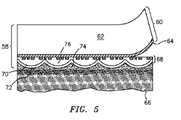
図5で最も良く示される第5の例示的実施形態では、本発明のシステムは、特に、キャリア基板62と剥離コーティング64とから構成される剥離ライナー60を更に含む、転写可能凹面反射光学システム58である。図5は転写可能凹面反射光学システムに関するが、上述の凸面反射光学システムも転写可能である。 In a fifth exemplary embodiment best shown in FIG. 5, the system of the present invention further comprises a
図5は、合成画像表示システム68が剥離ライナー60に剥離可能に結合された、紙基板66に適用中のシステム58を示す。一般に、剥離コーティング64は、周囲条件における接合を可能にし、次に機械的、化学的、熱的、及び光で誘起される分離技術を使用して転写時に剥離される、1~10ミクロンの間の厚さにおいて適用される機能性剥離コーティングである。例えば、熱及び圧力活性型の剥離が望ましい場合、キャリア基板62(例えば15~50ミクロンの間の厚さを有するUV透過性PETフィルム層)は、周囲温度において良好な付着性を有するコーティングであって、しかし、例えば連続ウェブプロセスにおいて熱及び圧力を適用するデスクトップドキュメントラミネータ内又は工業用箔押し機上での、ラミネート時の熱及び圧力の適用で軟化及び剥離する、コーティングを含む。好適な機能性剥離コーティングの例は、以下に限定されないが、ポリエチレン、ポリプロピレン、シリコーン、又は炭化水素蝋などの、低表面エネルギー材料を含む。所望される温度における剥離を提供するための、適切なガラス転移温度(Tg)を有する粘着付与樹脂及びモノマーを用いて配合された、高温において接合強度が大幅に弱まる感圧性接着剤も好適である。 FIG. 5 shows a
反射層(例えば蒸着された金属層)70、省略可能な保護コーティング72、及び接着剤層74が、集光要素76の配列上に示されている。反射層は、アルミニウム、クロム、銅、金、ニッケル、銀、ステンレス鋼、スズ、チタン、硫化亜鉛、フッ化マグネシウム、二酸化チタン、又は所望されるレベルの反射率を提供するその他の材料を使用して作られる、コンフォーマルコーティングされる反射層である。この層は、物理蒸着法(PVD)、化学蒸着法(CVD)、又はその他の好適なプロセスを使用して、約50ナノメートル~約2ミクロンの範囲の厚さにおいて適用されてもよい。反射層を保護する働きをする省略可能な保護コーティング72は、エネルギー硬化性アクリレート(例えば、着色又は補強特性を有する有機又は無機充填剤を含むエネルギー硬化性アクリレート)から、あるいはアクリル樹脂、エポキシ、EVA、ポリウレタン、PAVなどのような、溶剤又は水ベースのコーティングから作られてもよく、約1~約10ミクロンの範囲の厚さにおいて適用されてもよく、一方、接着剤層は、アクリル樹脂、シアノアクリレート、エポキシ、ポリイミド、ポリウレタン、ポリビニルアセテート、ゴム、及びシリコーンを含む、これらの対象面の間の接合を提供するように選択された熱活性型接着剤(すなわちホットメルト又はヒートシール接着剤)、感圧性接着剤、あるいは任意の熱硬化性又は熱可塑性接着剤系から作られてもよく、好ましくは、半硬化した熱活性型接着剤(例えば水ベースのポリウレタン)から作られ、約1~約10ミクロンの範囲の厚さにおいて適用される。 A reflective layer (eg, a vapor-deposited metal layer) 70, an optional
本発明の転写可能反射光学システムを製造する一例示的方法は、
硬化性樹脂材料を剥離ライナー(例えば、機能性剥離コーティングを有する滑らかな又は非構造化キャリア基板)の表面に適用し、表面を硬質のアイコンモールドに対して硬化させて、硬化性樹脂材料の表面内に、空隙の形態での画像アイコンの1つ以上の配列を形成し、
硬化性樹脂材料とのコントラストを提供する材料を用いて空隙を充填して、充填された画像アイコン層を形成し、充填された画像アイコン層の表面に硬化性樹脂材料を適用し、負レンズ形状を有する硬質の表面(すなわち負レンズモールド)に対して樹脂を硬化させて、硬化性樹脂材料の表面上に集光要素の1つ以上の配列を形成し、
金属又はその他の反射材料のコンフォーマルコーティングを集光要素に適用して、反射集光要素の1つ以上の配列を形成し、
必要に応じて、1つ以上の保護コーティング層を反射集光要素の1つ以上の配列に適用し、
1つ以上の接着剤層(例えば、半硬化した熱活性型接着剤層)を、反射集光要素の、1つ以上の必要に応じて保護コーティングされた配列に適用することを含む。An exemplary method for manufacturing transferable catoptric systems of the invention is
A curable resin material is applied to the surface of a release liner (eg, a smooth or unstructured carrier substrate with a functional release coating) and the surface is cured against a rigid icon mold to surface the curable resin material. Within, form one or more arrays of image icons in the form of voids,
The voids are filled with a material that provides contrast with the curable resin material to form a filled image icon layer, and the curable resin material is applied to the surface of the filled image icon layer to form a negative lens shape. The resin is cured against a hard surface (ie, negative lens mold) with a curable resin material to form an array of one or more condensing elements on the surface of the curable resin material.
A conformal coating of metal or other reflective material is applied to the light-collecting elements to form one or more arrays of the reflective light-collecting elements.
If desired, one or more protective coating layers may be applied to one or more arrays of reflective light-collecting elements.
It comprises applying one or more adhesive layers (eg, a semi-cured thermoactive adhesive layer) to one or more optionally protectively coated arrangements of reflective light collecting elements.
もたらされるフィルム状構造は、従来の転写フィルムと同様に処理/変換/転写されてもよい。言い換えると、この構造は対象基板(例えば紙幣、ID文書、又は製品パッケージ)と接触させられてもよく、そして、熱及び圧力が加えられたら、剥離ライナーが完全に剥がされて、合成画像表示システムのみが最終基板上に残されてもよい。 The resulting film-like structure may be processed / converted / transferred in the same manner as a conventional transfer film. In other words, this structure may be in contact with the subject substrate (eg banknote, ID document, or product package), and when heat and pressure are applied, the release liner is completely removed and the composite image display system. Only may be left on the final substrate.
本発明のシステムを対象基板に転写する連続転写プロセスの一例では、Leonard Kurz Stiftung & Co.KG(レオナード・クルツ・シュティフトゥンク・ウント・コー・カーゲー)から入手可能なホットスタンピングマシン(モデル番号MHA840)を採用する。このプロセスでは、最大6つのフィルム状構造の形態のシステムが、原紙上に(横方向(CD)で)正しく位置合わせして配置され、ホットスタンピングマシン上のカウンターホイールペア(counter wheel pairs)がフィルム状構造に圧力(550ニュートン(N)/ホイール)を加え、これにより、半硬化した熱活性型接着剤層の活性化が引き起こされる。次に、剥離ライナーが基本構造から分離されて、共通シリンダー上に巻き戻される。一般的なマシン設定は、速度(100~120メートル/分)、温度(135~160℃)である。 In an example of a continuous transfer process in which the system of the present invention is transferred to a target substrate, Leonard Kurz Staffung & Co., Ltd. A hot stamping machine (model number MHA840) available from KG (Leonard Kurtz Stiftunk und Ko Kage) will be adopted. In this process, a system in the form of up to six film structures is correctly aligned (horizontally (CD)) on the base paper and counter wheel pressures on a hot stamping machine are filmed. Pressure is applied to the shaped structure (550 Newtons (N) / wheel), which causes activation of the semi-cured thermoactive adhesive layer. The release liner is then separated from the basic structure and rewound onto a common cylinder. Typical machine settings are speed (100-120 meters / minute) and temperature (135-160 ° C).
一般的に言えば、反射システムが最終基板(例えば紙)に確実に転写されるためには、基板と反射システムとの間の接着剤接合強度が、反射システムを剥離ライナーに保持する接合より大きくなければならない。そのような配列のための一般的な接合強度は、反射システムと基板との間の接合について10~100ニュートン毎平方インチ(N/in2)(1.55~15.5N/cm2)の範囲内、及び反射システムと剥離ライナーとの間の接合について0.1~10N/in2(0.0155~1.55N/cm2)の範囲内であってもよい。Generally speaking, to ensure that the reflective system is transferred to the final substrate (eg paper), the adhesive bond strength between the substrate and the reflective system is greater than the bond that holds the reflective system on the release liner. There must be. Typical bond strengths for such arrangements are 10 to 100 Newtons per square inch (N / in2 ) (1.55 to 15.5 N / cm2 ) for the bond between the reflection system and the substrate. It may be in the range of 0.1 to 10 N / in2 (0.0155 to 1.55 N / cm2 ) for the junction between the reflection system and the release liner.
回折システム実施形態
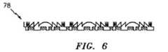
第6の例示的実施形態では、本発明のシステムは、必要に応じて転写可能な回折光学システムである。回折集光要素も入射光の集束を提供し、これらの集光要素を使用して作られたシステムは、同程度のf値を有する上述の屈折及び反射システムより薄く、回折光学システムの全体の厚さは約3~約50ミクロン(好ましくは約5~約10ミクロン)の範囲である。Diffraction System Embodiment In the sixth exemplary embodiment, the system of the present invention is a diffraction optical system that can be transferred as needed. Diffraction focusing elements also provide focusing of incident light, and systems made using these focusing elements are thinner than the refraction and reflection systems described above with similar f-numbers, and the entire diffractive optical system. The thickness ranges from about 3 to about 50 microns (preferably about 5 to about 10 microns).
本発明の回折光学システムでは、上述の屈折及び反射システムで使用された集光要素について識別されたものと同じ材料を使用して作られた回折集光要素を採用する。これらの回折集光要素は、約100ミクロン未満(より好ましくは約75ミクロン未満、及び最も好ましくは約15~約50ミクロン)の好ましい幅/ベース直径を有する。 The diffractive optical system of the present invention employs diffractive condensing elements made using the same materials identified for the condensing elements used in the refraction and reflection systems described above. These diffractive condensing elements have a preferred width / base diameter of less than about 100 microns (more preferably less than about 75 microns, and most preferably about 15 to about 50 microns).
これらの回折集光要素は、回折フレネルレンズ、フレネルゾーンプレートレンズ、ハイブリッド屈折/回折レンズ、及びこれらの組み合わせの群から選択される。一例示的実施形態では、回折フレネルレンズが使用され、そのようなレンズのそれぞれは、共通の焦点を有する一連の同心環状リングを有する。同心リングは共通平面内にあるため、各レンズは同様のf値を有する屈折レンズと比較して極めて平坦となる。相次ぐリングは、連続した曲率を最大効率のために有してもよく、あるいは、曲率は任意の数のステップ又は位相レベルによって近似されてもよい。最も単純な回折フレネルレンズ近似は、2つのみのステップを有し、フレネルゾーンプレート又はバイナリフレネルレンズとして知られている。より複雑な近似は、複雑さが増す順に、クォータナリ(quaternary)、8レベル、16レベル、及びアナログである。好ましい実施形態では、回折フレネルレンズはアナログプロファイルレンズである。 These diffractive condensing elements are selected from a group of diffractive Fresnel lenses, Fresnel zone plate lenses, hybrid refraction / diffractive lenses, and combinations thereof. In one exemplary embodiment, diffractive Fresnel lenses are used, each of which has a series of concentric annular rings with a common focal point. Since the concentric rings are in a common plane, each lens is extremely flat as compared to a refracting lens having a similar f-number. The successive rings may have a continuous curvature for maximum efficiency, or the curvature may be approximated by any number of steps or phase levels. The simplest diffractive Fresnel lens approximation has only two steps and is known as a Fresnel zone plate or binary Fresnel lens. More complex approximations are quaternary, 8-level, 16-level, and analog, in order of increasing complexity. In a preferred embodiment, the diffractive Fresnel lens is an analog profile lens.
本発明の回折光学システムで使用される構造化画像アイコンは、上述の屈折及び反射システムで使用されるものと同様である。 The structured image icons used in the diffractive optical system of the present invention are similar to those used in the refraction and reflection systems described above.
回折集光要素は、波長の変化に影響されやすく、強い色収差を受けることが知られている。しかし、本発明のシステムでは、回折集光要素は、透過性(図6の回折光学システム78を参照)又は反射性(図7の回折光学システム80を参照)のいずれかである。どちらのシステムでも、構造化画像アイコンは、関連する回折集光要素(例えばフレネルレンズ)の焦点深さと交わり、これは光学スペーサを使用せずに達成される。 It is known that the diffraction and condensing element is easily affected by a change in wavelength and is subject to strong chromatic aberration. However, in the system of the present invention, the diffractive condensing element is either transmissive (see diffractive
必要に応じて転写可能な透過性回折光学システム78は、屈折レンズモールドの形状が、回折レンズを生成するのに好適な形状に置き換えられることを除き、第1の例示的実施形態と同じ方法及び材料構成を使用して生成される。この光学システムは、また、第2の例示的実施形態で詳述した技術を使用して、そのキャリア基板から転写されてもよい。 The transmissible diffractive
必要に応じて転写可能な反射モード回折光学システム80は、反射レンズモールドの形状が、反射スタイルの回折レンズを生成するのに好適な形状に置き換えられ、続いてこれが金属化されることを除き、第3の例示的実施形態と同じ方法及び材料構成を使用して生成される。この光学システムは、第5の例示的実施形態で詳述した反射性転写のための技術を使用して、そのキャリア基板から同様に転写されてもよい。 The reflection mode diffractive
本発明は、本発明のシステムから作られた、又は本発明のシステムを使用した繊維質及び非繊維質のシート材料、並びに、これらの材料から作られた文書を更に提供する。本明細書中で使用される用語「文書」は、紙幣又は貨幣、債券、小切手、トラベラーズチェック、宝くじ券、郵便切手、株券、権利証書などの経済的価値を有する任意の種類の文書、あるいはパスポート、IDカード、運転免許証などの身分証明書、あるいはラベルなどの非セキュア文書を示す。本発明の光学システムは、また、物品(消費者向け又は非消費者向け物品)、及び、これらの物品と共に使用されるバッグ、パッケージ、又はラベルと共に使用することが企図される。 The present invention further provides fibrous and non-fibrous sheet materials made from or using the systems of the invention, as well as documents made from these materials. As used herein, the term "document" refers to any type of document of economic value, such as banknotes or money, bonds, checks, travelers checks, lottery tickets, postal stamps, stock certificates, certificates of title, or passports. , ID card, identification card such as driver's license, or non-secure document such as label. The optical system of the present invention is also intended for use with articles (consumer or non-consumer articles) and bags, packages, or labels used with these articles.
本発明のシステムの、その他の企図される最終使用適用例は、広告及びマルチメディアディスプレー(例えば広告板、交通及び工業安全標識、マーケティング又は展示会の目的のための商業ディスプレー)、車両の外観を向上させるための製品(例えばステッカー、全面広告)、装飾ラップ及び壁紙、シャワーカーテン、芸術ディスプレーなどのような、より大きな寸法の画像を投射する製品を含む。 Other intended end-use applications of the system of the invention are advertising and multimedia displays (eg, billboards, traffic and industrial safety signs, commercial displays for marketing or exhibition purposes), vehicle appearance. Includes products that project larger dimensional images, such as products for improvement (eg stickers, full-page advertisements), decorative wraps and wallpapers, shower curtains, art displays, etc.
本発明のその他の特徴及び利点は、詳細な説明及び添付の図面から、当業者にとって明らかとなるであろう。特に定義しない限り、本明細書中で使用される全ての技術及び科学用語は、この発明が属する技術分野の当業者によって一般的に理解されるものと同じ意味を有する。本明細書中で言及される全ての出版物、特許出願、特許、及びその他の参考文献は、それらの全体が参照によって本明細書中に援用される。矛盾がある場合は、定義を含めて本明細書が優先される。加えて、材料、方法、及び実施例は、例示にすぎず、限定することを意図するものではない。 Other features and advantages of the present invention will be apparent to those skilled in the art from detailed description and accompanying drawings. Unless otherwise defined, all technical and scientific terms used herein have the same meaning as commonly understood by one of ordinary skill in the art to which this invention belongs. All publications, patent applications, patents, and other references referred to herein are incorporated herein by reference in their entirety. In the event of inconsistencies, this specification, including definitions, will prevail. In addition, the materials, methods, and examples are merely exemplary and are not intended to be limiting.
Claims (15)
Translated fromJapanese凸面反射要素の配列と、
前記凸面反射要素の配列の上に位置する画像アイコンの配列と、
前記凸面反射要素の配列と前記画像アイコンの配列との間の間隙空間を満たす充填層と、
を備え、
前記凸面反射要素の配列の各凸面反射要素は、遠くの光源によって照らされた場合に光点を生じさせるように構成された反射面を備え、
前記画像アイコンの配列の各画像アイコンは、前記光点の視界を少なくとも部分的に遮る材料の領域を備え、
前記充填層は一方の面において前記凸面反射要素の配列に当接するとともに、前記画像アイコンの配列は、前記充填層の他方の面上に位置し、
前記凸面反射要素の配列及び前記画像アイコンの配列は、遮られた光点と遮られていない光点とのパターンを形成するように、協働し、
前記遮られた光点と遮られていない光点とのパターンは、合成画像を形成する、
光学システム。An optical system with reduced thickness,
An array of convex reflective elements and
An array of image icons located above the array of convex reflective elements,
A packed bed that fills the gap space between the array of convex reflective elements and the array of image icons.
Equipped with
Each convex reflective element in the array of convex reflective elements comprises a reflective surface configured to produce a light spot when illuminated by a distant light source.
Each image icon in the array of image icons comprises an area of material that at least partially obstructs the view of the light spot.
The packed bed abuts on one surface the array of convex reflective elements, and the array of image icons is located on the other surface of the packed bed.
The array of convex reflective elements and the array of image icons work together to form a pattern of blocked and unobstructed light spots.
The pattern of the blocked and unobstructed light spots forms a composite image.
Optical system.
学システム。The optical system according to claim 1, wherein the reflecting surface configured to generate the light spot is an aspherical surface.
凸面反射要素の配列を提供することと、
画像アイコンの配列を前記凸面反射要素の配列の上に提供することと、
前記凸面反射要素の配列と前記画像アイコンの配列との間の間隙空間を満たす充填層を設けることと、
を備え、
前記凸面反射要素の配列の各凸面反射要素は、遠くの光源によって照らされた場合に光点を生じさせるように構成された反射面を備え、
前記画像アイコンの配列の各画像アイコンは、視線方向の光点の視界を少なくとも部分的に遮る材料の領域を備え、
前記充填層は一方の面において前記凸面反射要素の配列に当接するとともに、前記画像アイコンの配列は、前記充填層の他方の面上に位置し、
前記凸面反射要素の配列及び前記画像アイコンの配列は、遮られた及び遮られていない光点のパターンを形成するように、協働し、
前記遮られた及び遮られていない光点のパターンは、合成画像を形成する、
光学システムの製造方法。It is a manufacturing method of an optical system.
To provide an array of convex reflective elements,
Providing an array of image icons on top of the array of convex reflective elements,
A packed bed that fills the gap space between the array of convex reflective elements and the array of image icons is provided.
Equipped with
Each convex reflective element in the array of convex reflective elements comprises a reflective surface configured to produce a light spot when illuminated by a distant light source.
Each image icon in the array of image icons comprises an area of material that at least partially obstructs the view of the light spot in the line-of-sight direction.
The packed bed abuts on one surface the array of convex reflective elements, and the array of image icons is located on the other surface of the packed bed.
The array of convex reflective elements and the array of image icons work together to form a pattern of blocked and unobstructed light spots.
The patterns of blocked and unobstructed light spots form a composite image.
How to manufacture an optical system.
前記凸面反射要素の配列を提供することは、
材料の層を成形することと、
金属で前記材料の層をコーティングすることと、
を備える、請求項9に記載の光学システムの製造方法。The array of convex reflective elements is formed on top of the array of image icons.
Providing an array of the convex reflective elements
Forming layers of material and
By coating the layer of the material with metal,
9. The method of manufacturing an optical system according to claim 9.
The method for manufacturing an optical system according to claim 9, wherein the reflecting surface configured to generate the light spot is a spherical surface.
Applications Claiming Priority (3)
| Application Number | Priority Date | Filing Date | Title |
|---|---|---|---|
| US201161525239P | 2011-08-19 | 2011-08-19 | |
| US61/525,239 | 2011-08-19 | ||
| JP2020143928AJP2021005092A (en) | 2011-08-19 | 2020-08-27 | Optical system and optical system manufacturing method |
Related Parent Applications (1)
| Application Number | Title | Priority Date | Filing Date |
|---|---|---|---|
| JP2020143928ADivisionJP2021005092A (en) | 2011-08-19 | 2020-08-27 | Optical system and optical system manufacturing method |
Publications (2)
| Publication Number | Publication Date |
|---|---|
| JP2022093467Atrue JP2022093467A (en) | 2022-06-23 |
| JP7381023B2 JP7381023B2 (en) | 2023-11-15 |
Family
ID=46970382
Family Applications (4)
| Application Number | Title | Priority Date | Filing Date |
|---|---|---|---|
| JP2014527203APendingJP2014524600A (en) | 2011-08-19 | 2012-08-17 | Optical system capable of transfer on demand with reduced thickness |
| JP2018239264APendingJP2019070826A (en) | 2011-08-19 | 2018-12-21 | Optical system having reduced thickness transferable as required |
| JP2020143928APendingJP2021005092A (en) | 2011-08-19 | 2020-08-27 | Optical system and optical system manufacturing method |
| JP2022073147AActiveJP7381023B2 (en) | 2011-08-19 | 2022-04-27 | Transferable optical system on demand with reduced thickness |
Family Applications Before (3)
| Application Number | Title | Priority Date | Filing Date |
|---|---|---|---|
| JP2014527203APendingJP2014524600A (en) | 2011-08-19 | 2012-08-17 | Optical system capable of transfer on demand with reduced thickness |
| JP2018239264APendingJP2019070826A (en) | 2011-08-19 | 2018-12-21 | Optical system having reduced thickness transferable as required |
| JP2020143928APendingJP2021005092A (en) | 2011-08-19 | 2020-08-27 | Optical system and optical system manufacturing method |
Country Status (13)
| Country | Link |
|---|---|
| US (1) | US10890692B2 (en) |
| EP (3) | EP3244254B1 (en) |
| JP (4) | JP2014524600A (en) |
| KR (1) | KR101948363B1 (en) |
| CN (1) | CN104024921B (en) |
| AU (1) | AU2012299113B2 (en) |
| BR (1) | BR112014003888A2 (en) |
| CA (1) | CA2845610C (en) |
| ES (2) | ES2902474T3 (en) |
| IN (1) | IN2014CN02023A (en) |
| MX (1) | MX372840B (en) |
| RU (1) | RU2641316C9 (en) |
| WO (1) | WO2013028534A1 (en) |
Families Citing this family (47)
| Publication number | Priority date | Publication date | Assignee | Title |
|---|---|---|---|---|
| CA2845610C (en) | 2011-08-19 | 2020-08-25 | Visual Physics, Llc | Optionally transferable optical system with a reduced thickness |
| US9572897B2 (en) | 2012-04-02 | 2017-02-21 | Modernatx, Inc. | Modified polynucleotides for the production of cytoplasmic and cytoskeletal proteins |
| RU2621558C9 (en) | 2012-08-17 | 2017-12-05 | Визуал Физикс, Ллс | Process of transfering microstructures on final substrate |
| ES2728508T3 (en) | 2013-03-15 | 2019-10-25 | Visual Physics Llc | Optical safety device |
| US9873281B2 (en) | 2013-06-13 | 2018-01-23 | Visual Physics, Llc | Single layer image projection film |
| KR101341072B1 (en)* | 2013-09-04 | 2013-12-19 | 안재광 | Label for identifying genuine article comprising multiple nano structure and stereoscopic lens |
| EP2908341B1 (en)* | 2014-02-18 | 2018-07-11 | ams AG | Semiconductor device with surface integrated focusing element |
| SG11201607093YA (en)* | 2014-02-27 | 2016-09-29 | Philip Morris Products Sa | Combustible heat source having a barrier affixed thereto and method of manufacture thereof |
| US10766292B2 (en) | 2014-03-27 | 2020-09-08 | Crane & Co., Inc. | Optical device that provides flicker-like optical effects |
| RU2687171C9 (en) | 2014-03-27 | 2019-07-22 | Визуал Физикс, Ллс | An optical device that produces flicker-like optical effects |
| CN103984111A (en)* | 2014-05-26 | 2014-08-13 | 上海和辉光电有限公司 | Polarization structure achieving naked eye 3D function and manufacturing method thereof |
| WO2016011249A2 (en)* | 2014-07-17 | 2016-01-21 | Visual Physics, Llc | An improved polymeric sheet material for use in making polymeric security documents such as banknotes |
| ES3027557T3 (en) | 2014-09-16 | 2025-06-16 | Crane Security Tech Inc | Secure lens layer |
| DE102014113966A1 (en) | 2014-09-26 | 2016-03-31 | Carl Zeiss Jena Gmbh | Method for producing an optical element |
| CN106715603B (en) | 2014-10-03 | 2020-05-19 | 恩图鲁斯特咨询卡有限公司 | Surface Covering Film Feeds, Surface Covering Layers, Plastic Cards |
| BR112017017113B1 (en) | 2015-02-11 | 2022-09-27 | Crane & Co., Inc | FIBROUS SHEET MATERIAL AND METHOD FOR APPLICATION TO THE SURFACE OF A SAFETY DEVICE ON A FIBROUS SHEET MATERIAL |
| NL2014520B1 (en)* | 2015-03-25 | 2017-01-19 | Morpho Bv | Method of providing an imprinted security feature. |
| US11143794B2 (en) | 2015-07-08 | 2021-10-12 | Shine Optoelectronics (Kunshan) Co., Ltd | Optical film |
| WO2017005206A1 (en) | 2015-07-08 | 2017-01-12 | 昇印光电(昆山)股份有限公司 | Optical film |
| KR102563684B1 (en) | 2015-08-27 | 2023-08-09 | 크레인 시큐리티 테크놀로지스, 인크. | Single or double transfer process for preparing and transferring sharply formed single elements to the object to be protected |
| CN106597581A (en)* | 2015-10-14 | 2017-04-26 | 昇印光电(昆山)股份有限公司 | Micro-optics imaging film and image device |
| CN109314193B (en)* | 2016-05-31 | 2021-01-15 | 大日本印刷株式会社 | Battery packaging material and method for producing the same, battery and polyester film |
| WO2017214481A1 (en)* | 2016-06-10 | 2017-12-14 | Corning Incorporated | Microstructured and patterned light guide plates and devices comprising the same |
| US10864762B2 (en) | 2016-08-15 | 2020-12-15 | Visual Physics, Llc | Anti-harvestable security feature |
| MX2019009459A (en) | 2017-02-10 | 2019-12-16 | Crane & Co Inc | Machine-readable optical security device. |
| US20180247170A1 (en) | 2017-02-10 | 2018-08-30 | Crane & Co., Inc. | Authentication and anti-harvesting security feature with machine detectable indicia |
| CN106842388B (en)* | 2017-04-06 | 2019-02-12 | 中国科学院光电技术研究所 | Forming method of multi-focus bionic compound eye structure |
| CN107643555A (en)* | 2017-08-25 | 2018-01-30 | 张家港康得新光电材料有限公司 | Multilayer complex films and preparation method thereof |
| CN107805974B (en)* | 2017-11-17 | 2024-06-04 | 苏州苏大维格科技集团股份有限公司 | Transfer paper, manufacturing method thereof and tobacco box |
| CN107794807B (en)* | 2017-11-17 | 2024-06-04 | 苏州苏大维格科技集团股份有限公司 | Transfer paper and manufacturing method thereof |
| KR102667602B1 (en) | 2018-01-03 | 2024-05-22 | 비쥬얼 피직스 엘엘씨 | Micro optical security device with interactive dynamic security features |
| CN110244459B (en)* | 2018-03-09 | 2021-10-08 | 财团法人工业技术研究院 | Augmented reality device |
| EP4421762A3 (en) | 2018-07-03 | 2024-12-04 | Crane & Co., Inc. | Security document with attached security device which demonstrates increased harvesting resistance |
| EP3860862B1 (en)* | 2018-10-05 | 2022-09-07 | Sicpa Holding Sa | A method of designing a light-redirecting surface of a caustic layer, an optical security element comprising the designed light-redirecting surface of the caustic layer, a marked object, use and method of authenticating the object |
| EP3902685A4 (en) | 2018-12-27 | 2022-12-28 | Crane & Co., Inc. | Surface applied micro-optic anti-counterfeit security device |
| CN109979310A (en)* | 2019-05-17 | 2019-07-05 | 四川芯辰光微纳科技有限公司 | A kind of picture and text protection structure and preparation method thereof based on dynamic anti-fake film |
| JP7646569B2 (en) | 2019-05-20 | 2025-03-17 | クレイン アンド カンパニー、 インコーポレイテッド | Use of nanoparticles to tailor the refractive index of a layer of a polymer matrix to optimize micro-optical (MO) focusing - Patent Application 20070233633 |
| KR102264589B1 (en)* | 2019-09-09 | 2021-06-11 | 안병학 | Product Of Lenticular Transferring Printed Matter Heat-Adhered By Hot-Melt Resin |
| CN112572016B (en)* | 2019-09-30 | 2022-05-24 | 中钞特种防伪科技有限公司 | Optical anti-counterfeiting element and anti-counterfeiting product |
| CN113778270B (en)* | 2020-08-05 | 2024-10-18 | 北京沃东天骏信息技术有限公司 | Method and device for dragging icon |
| CN112021910A (en)* | 2020-09-02 | 2020-12-04 | 浙江元正布艺有限公司 | Yarn composite curtain and manufacturing method thereof |
| CN114537015B (en) | 2020-11-24 | 2023-03-31 | 中钞特种防伪科技有限公司 | Optical anti-fake element and product thereof |
| CN115674933B (en)* | 2021-07-28 | 2025-09-12 | 中钞特种防伪科技有限公司 | A customizable anti-counterfeiting element and anti-counterfeiting product |
| DE102022001915A1 (en) | 2022-06-01 | 2023-12-07 | Giesecke+Devrient Currency Technology Gmbh | Security element transfer material for transferring security elements with a micro-optical authenticity feature and method for its production |
| NL2035169B1 (en)* | 2023-06-24 | 2025-01-07 | Dimenco Holding B V | Crosstalk reduction in an autostereoscopic display device |
| CN116909107B (en)* | 2023-07-25 | 2024-03-01 | 上海图双精密装备有限公司 | Light source system for illumination of lithography equipment |
| WO2025193748A1 (en) | 2024-03-11 | 2025-09-18 | Crane & Co., Inc. | Single-sided micro-optic security device |
Citations (21)
| Publication number | Priority date | Publication date | Assignee | Title |
|---|---|---|---|---|
| US5568313A (en)* | 1992-08-18 | 1996-10-22 | Applied Physics Research, L.P. | Apparatus for providing autostereoscopic and dynamic images and method of manufacturing same |
| JP2000056103A (en)* | 1998-08-11 | 2000-02-25 | Seiko Epson Corp | Microlens array, method of manufacturing the same, and display device |
| JP2002122709A (en)* | 2000-10-16 | 2002-04-26 | Seiko Epson Corp | Substrate with microlens array, electro-optical device, manufacturing method thereof, and projection display device |
| JP2002518914A (en)* | 1998-06-12 | 2002-06-25 | フォーディー−ビジョン ゲーエムベーハー | 3D display system |
| US20030137740A1 (en)* | 2001-02-09 | 2003-07-24 | Michael Hannington | Rear projection screens and light filters with conformable coatings and methods of making the same |
| JP2003227903A (en)* | 2002-02-05 | 2003-08-15 | Seiko Epson Corp | Microlens array plate and its manufacturing method, optical element plate and its manufacturing method, electro-optical device, and electronic equipment |
| JP2006215162A (en)* | 2005-02-02 | 2006-08-17 | Dainippon Printing Co Ltd | Reflective screen and reflective projection system |
| JP2007514188A (en)* | 2003-11-21 | 2007-05-31 | ナノヴェンションズ インコーポレイテッド | Micro optical security and image display system |
| JP2008545550A (en)* | 2005-05-18 | 2008-12-18 | ナノベンションズ ホールディングズ エルエルシー | Image display system and micro optical security system |
| US20090008923A1 (en)* | 2005-12-23 | 2009-01-08 | Giesecke & Devrient Gmbh | Security Element |
| JP2009015195A (en)* | 2007-07-09 | 2009-01-22 | Seiko Epson Corp | Reflective screen |
| US20090034082A1 (en)* | 2004-04-30 | 2009-02-05 | De La Rue International, Ltd. | Optically Variable Devices |
| JP2009536885A (en)* | 2006-05-12 | 2009-10-22 | クレイン アンド カンパニー インコーポレーテッド | A micro-optical film structure that projects a spatially coordinated image by static and / or other projected images, alone or with a security document or label |
| JP2009543138A (en)* | 2006-06-28 | 2009-12-03 | ビジュアル フィジクス エルエルシー | Micro optical security and image display system |
| US20100103527A1 (en)* | 2008-10-23 | 2010-04-29 | 3M Innovative Properties Company | Methods of forming sheeting with composite images that float and sheeting with composite images that float |
| US20100182221A1 (en)* | 2007-06-25 | 2010-07-22 | Giesecke & Devrient Gmbh | Representation system |
| WO2010113114A2 (en)* | 2009-03-30 | 2010-10-07 | Arjowiggins Security | Security element comprising basic reflective structures |
| JP2011502811A (en)* | 2007-10-15 | 2011-01-27 | オーファウデー キネグラム アーゲー | Multilayer body and method of making the multilayer body |
| WO2011019912A1 (en)* | 2009-08-12 | 2011-02-17 | Visual Physics, Llc | A tamper indicating optical security device |
| WO2011090625A2 (en)* | 2009-12-30 | 2011-07-28 | 3M Innovative Properties Company | Light directing sign substrate |
| US20130044362A1 (en)* | 2010-03-01 | 2013-02-21 | De La Rue International Limited | Optical device |
Family Cites Families (313)
| Publication number | Priority date | Publication date | Assignee | Title |
|---|---|---|---|---|
| US992151A (en) | 1909-02-04 | 1911-05-16 | Rodolphe Berthon | Apparatus for color photography. |
| US1824353A (en) | 1926-12-15 | 1931-09-22 | Jensen Rasmus Olaf Jonas | Screen for showing projected images in lighted rooms and for shortexposure photography |
| US1849036A (en) | 1926-12-23 | 1932-03-08 | Victor C Ernst | Photographic process and auxiliary element therefor |
| US1942841A (en) | 1931-01-19 | 1934-01-09 | Shimizu Takeo | Daylight screen |
| US2268351A (en) | 1938-08-25 | 1941-12-30 | Tanaka Nawokich | Means for presenting pictures in apparent three dimensions |
| US2355902A (en) | 1941-04-10 | 1944-08-15 | Photoplating Company | Sign with animated effect |
| US2432896A (en) | 1945-03-12 | 1947-12-16 | Hotchner Fred | Retroreflective animation display |
| NL110404C (en) | 1955-03-29 | |||
| US2888855A (en) | 1956-08-23 | 1959-06-02 | Tanaka Nawokich | Means for presenting pictures in three dimensional effect |
| US3122853A (en) | 1961-08-10 | 1964-03-03 | John C Koonz | Fishing lure |
| US3264164A (en) | 1962-04-30 | 1966-08-02 | Toscony Inc | Color dynamic, three-dimensional flexible film and method of making it |
| US3241429A (en) | 1962-05-14 | 1966-03-22 | Pid Corp | Pictorial parallax panoramagram units |
| US3357772A (en) | 1963-02-27 | 1967-12-12 | Rowland Products Inc | Phased lenticular sheets for optical effects |
| GB1095286A (en) | 1963-07-08 | 1967-12-13 | Portals Ltd | Security device for use in security papers |
| US3312006A (en) | 1964-03-11 | 1967-04-04 | Rowland Products Inc | Motion displays |
| JPS414953Y1 (en) | 1964-07-28 | 1966-03-18 | ||
| US3357773A (en) | 1964-12-31 | 1967-12-12 | Rowland Products Inc | Patterned sheet material |
| JPS4622600Y1 (en) | 1965-07-02 | 1971-08-05 | ||
| US3463581A (en) | 1966-01-17 | 1969-08-26 | Intermountain Res & Eng | System for three-dimensional panoramic static-image motion pictures |
| US3811213A (en) | 1968-11-17 | 1974-05-21 | Photo Motion Corp | Moire motion illusion apparatus and method |
| JPS4941718B1 (en) | 1968-12-30 | 1974-11-11 | ||
| US3643361A (en) | 1969-11-17 | 1972-02-22 | Photo Motion Corp | Moire motion illusion apparatus |
| BE789941A (en) | 1971-04-21 | 1973-02-01 | Waly Adnan | MINIATURIZED IMAGE RECORDING AND PLAYBACK SYSTEM |
| US3887742A (en) | 1972-04-13 | 1975-06-03 | Richard E Reinnagel | Copy resistant documents |
| US4025673A (en) | 1972-04-13 | 1977-05-24 | Reinnagel Richard E | Method of forming copy resistant documents by forming an orderly array of fibers extending upward from a surface, coating the fibers and printing the coated fibers and the copy resistant document resulting from said method |
| US3801183A (en) | 1973-06-01 | 1974-04-02 | Minnesota Mining & Mfg | Retro-reflective film |
| US4105318A (en) | 1974-05-30 | 1978-08-08 | Izon Corporation | Pinhole microfiche recorder and viewer |
| US4082426A (en) | 1976-11-26 | 1978-04-04 | Minnesota Mining And Manufacturing Company | Retroreflective sheeting with retroreflective markings |
| US4185191A (en) | 1978-06-05 | 1980-01-22 | Honeywell Inc. | Range determination system |
| US4498736A (en) | 1981-02-02 | 1985-02-12 | Griffin Robert B | Method and apparatus for producing visual patterns with lenticular sheets |
| US4892385A (en) | 1981-02-19 | 1990-01-09 | General Electric Company | Sheet-material authenticated item with reflective-diffractive authenticating device |
| US4417784A (en) | 1981-02-19 | 1983-11-29 | Rca Corporation | Multiple image encoding using surface relief structures as authenticating device for sheet-material authenticated item |
| US4345833A (en) | 1981-02-23 | 1982-08-24 | American Optical Corporation | Lens array |
| US4437935A (en) | 1981-06-03 | 1984-03-20 | Crane And Company | Method and apparatus for providing security features in paper |
| US4519632A (en) | 1982-03-19 | 1985-05-28 | Computer Identification Systems, Inc. | Identification card with heat reactive coating |
| DE3211102A1 (en) | 1982-03-25 | 1983-10-06 | Schwarz Klaus Billett Automat | METHOD FOR AUTHENTICITY CONTROL OF PAPER SECTIONS AND USE OF A COLOR REACTION SYSTEM SUITABLE FOR THIS |
| JPS58175091A (en) | 1982-04-06 | 1983-10-14 | 株式会社東芝 | Security strain detection device |
| US4814594A (en) | 1982-11-22 | 1989-03-21 | Drexler Technology Corporation | Updatable micrographic pocket data card |
| US4634220A (en) | 1983-02-07 | 1987-01-06 | Minnesota Mining And Manufacturing Company | Directionally imaged sheeting |
| US4645301A (en) | 1983-02-07 | 1987-02-24 | Minnesota Mining And Manufacturing Company | Transparent sheet containing authenticating image and method of making same |
| US4507349A (en) | 1983-05-16 | 1985-03-26 | Howard A. Fromson | Security medium and secure articles and methods of making same |
| EP0156460B1 (en) | 1984-01-31 | 1989-10-18 | Matsushita Electric Industrial Co., Ltd. | Pick-up arm for an optical disk player |
| NL8400868A (en) | 1984-03-19 | 1984-10-01 | Philips Nv | LAYERED OPTICAL COMPONENT. |
| US4534398A (en) | 1984-04-30 | 1985-08-13 | Crane & Co. | Security paper |
| US4691993A (en) | 1985-05-13 | 1987-09-08 | Minnesota Mining And Manufacturing Company | Transparent sheets containing directional images and method for forming the same |
| US4662651A (en) | 1985-05-31 | 1987-05-05 | The Standard Register Company | Document protection using multicolor characters |
| DE3687560D1 (en) | 1985-10-15 | 1993-03-04 | Gao Ges Automation Org | DATA CARRIER WITH AN OPTICAL AUTHENTICITY CHARACTER, AND METHOD FOR PRODUCING AND CHECKING THE DATA CARRIER. |
| US4920039A (en) | 1986-01-06 | 1990-04-24 | Dennison Manufacturing Company | Multiple imaging |
| US4935335A (en) | 1986-01-06 | 1990-06-19 | Dennison Manufacturing Company | Multiple imaging |
| DE3609090A1 (en) | 1986-03-18 | 1987-09-24 | Gao Ges Automation Org | SECURITY PAPER WITH SECURED THREAD STORED IN IT AND METHOD FOR THE PRODUCTION THEREOF |
| CH670904A5 (en) | 1986-07-10 | 1989-07-14 | Landis & Gyr Ag | |
| DE3741179A1 (en) | 1987-12-04 | 1989-06-15 | Gao Ges Automation Org | DOCUMENT WITH FALSE-PROOF SURFACE RELIEF AND METHOD FOR PRODUCING THE SAME |
| MY102798A (en) | 1987-12-04 | 1992-10-31 | Portals Ltd | Security paper for bank notes and the like |
| EP0723875B1 (en) | 1989-01-31 | 2001-11-07 | Dai Nippon Insatsu Kabushiki Kaisha | Methods for making heat transfer recordings and heat transfer image receiving sheets |
| JPH0355501A (en) | 1989-07-25 | 1991-03-11 | Nippon Sheet Glass Co Ltd | Lens array plate |
| US5085514A (en) | 1989-08-29 | 1992-02-04 | American Bank Note Holographics, Inc. | Technique of forming a separate information bearing printed pattern on replicas of a hologram or other surface relief diffraction pattern |
| US4988151A (en) | 1989-08-31 | 1991-01-29 | Hughes Aircraft Company | Method for making edge faded holograms |
| US5695346A (en) | 1989-12-07 | 1997-12-09 | Yoshi Sekiguchi | Process and display with moveable images |
| US5044707A (en) | 1990-01-25 | 1991-09-03 | American Bank Note Holographics, Inc. | Holograms with discontinuous metallization including alpha-numeric shapes |
| US5142383A (en) | 1990-01-25 | 1992-08-25 | American Banknote Holographics, Inc. | Holograms with discontinuous metallization including alpha-numeric shapes |
| US5438928A (en) | 1990-01-31 | 1995-08-08 | Thomas De La Rue & Company Limited | Signature panels |
| US6724536B2 (en) | 1990-05-18 | 2004-04-20 | University Of Arkansas | Directional image lenticular window sheet |
| US6870681B1 (en) | 1992-09-21 | 2005-03-22 | University Of Arkansas, N.A. | Directional image transmission sheet and method of making same |
| US5232764A (en) | 1990-06-04 | 1993-08-03 | Meiwa Gravure Co., Ltd. | Synthetic resin pattern sheet |
| US5135262A (en) | 1990-06-20 | 1992-08-04 | Alcan International Limited | Method of making color change devices activatable by bending and product thereof |
| WO1992000855A1 (en) | 1990-07-12 | 1992-01-23 | Thomas De La Rue & Company Limited | Improvements relating to signature panels |
| US5215864A (en) | 1990-09-28 | 1993-06-01 | Laser Color Marking, Incorporated | Method and apparatus for multi-color laser engraving |
| US5254390B1 (en) | 1990-11-15 | 1999-05-18 | Minnesota Mining & Mfg | Plano-convex base sheet for retroreflective articles |
| DE4036637A1 (en) | 1990-11-16 | 1992-05-21 | Gao Ges Automation Org | SECURITIES AND METHOD FOR THE PRODUCTION THEREOF |
| JP3120401B2 (en) | 1991-01-08 | 2000-12-25 | 日本ビクター株式会社 | Optical card |
| GB9106128D0 (en) | 1991-03-22 | 1991-05-08 | Amblehurst Ltd | Article |
| US5169707A (en) | 1991-05-08 | 1992-12-08 | Minnesota Mining And Manufacturing Company | Retroreflective security laminates with dual level verification |
| GB9113462D0 (en) | 1991-06-21 | 1991-08-07 | Pizzanelli David J | Laser-activated bar-code holograms and bar-code recognition system |
| US5384861A (en) | 1991-06-24 | 1995-01-24 | Picker International, Inc. | Multi-parameter image display with real time interpolation |
| US5211424A (en) | 1991-08-15 | 1993-05-18 | Prc Inc. | Secure passport document and method of making the same |
| US5538753A (en) | 1991-10-14 | 1996-07-23 | Landis & Gyr Betriebs Ag | Security element |
| US5626969A (en) | 1992-02-21 | 1997-05-06 | General Binding Corporation | Method of manufacturing film for lamination |
| WO1993024332A1 (en) | 1992-05-25 | 1993-12-09 | Reserve Bank Of Australia Trading As Note Printing Australia | Applying diffraction gratings to security documents |
| DK95292D0 (en) | 1992-07-23 | 1992-07-23 | Frithioff Johansen | PROCEDURE AND DISPLAY TO PROVIDE AN ENLARGED PICTURE OF A TWO-DIMENSIONAL PERIODIC PICTURE PATTERN |
| DE4243987C2 (en) | 1992-12-23 | 2003-10-09 | Gao Ges Automation Org | ID cards with visually visible authenticity |
| BE1006880A3 (en) | 1993-03-01 | 1995-01-17 | Solvay | Precurseur solid system of a catalyst for olefin polymerization, method of preparation, catalytic system including the solid precursor and method for polymerization of olefins in the presence of this system catalyst. |
| DE4314380B4 (en) | 1993-05-01 | 2009-08-06 | Giesecke & Devrient Gmbh | Security paper and process for its production |
| GB9309673D0 (en) | 1993-05-11 | 1993-06-23 | De La Rue Holographics Ltd | Security device |
| US5393099A (en) | 1993-05-21 | 1995-02-28 | American Bank Note Holographics, Inc. | Anti-counterfeiting laminated currency and method of making the same |
| US5449200A (en) | 1993-06-08 | 1995-09-12 | Domtar, Inc. | Security paper with color mark |
| US5574083A (en) | 1993-06-11 | 1996-11-12 | Rohm And Haas Company | Aromatic polycarbodiimide crosslinkers |
| US5393590A (en) | 1993-07-07 | 1995-02-28 | Minnesota Mining And Manufacturing Company | Hot stamping foil |
| US5555476A (en) | 1993-08-30 | 1996-09-10 | Toray Industries, Inc. | Microlens array sheet for a liquid crystal display, method for attaching the same and liquid crystal display equipped with the same |
| DE69432080T2 (en) | 1993-09-30 | 2004-01-22 | Grapac Japan Co., Inc. | METHOD FOR PRODUCING A LENS AND ITEM WITH A LENS, ITEM WITH LENS AND RESIN COMPOSITION THAT MAKES A SEPARATION |
| US6345104B1 (en) | 1994-03-17 | 2002-02-05 | Digimarc Corporation | Digital watermarks and methods for security documents |
| US5598281A (en) | 1993-11-19 | 1997-01-28 | Alliedsignal Inc. | Backlight assembly for improved illumination employing tapered optical elements |
| JPH07225303A (en) | 1993-12-16 | 1995-08-22 | Sharp Corp | Microlens substrate, liquid crystal display device using the same, and liquid crystal projector device |
| DE4344553A1 (en) | 1993-12-24 | 1995-06-29 | Giesecke & Devrient Gmbh | Security paper with a thread-like or ribbon-shaped security element and method for producing the same |
| GB9400942D0 (en) | 1994-01-19 | 1994-03-16 | De La Rue Thomas & Co Ltd | Copy indicating security device |
| US5460679A (en) | 1994-02-03 | 1995-10-24 | Triad Technologies International, Inc. | Method for producing three-dimensional effect |
| US5503902A (en) | 1994-03-02 | 1996-04-02 | Applied Physics Research, L.P. | Light control material |
| US6302989B1 (en) | 1994-03-31 | 2001-10-16 | Giesecke & Devrient Gmbh | Method for producing a laminar compound for transferring optically variable single elements to objects to be protected |
| US5464690A (en) | 1994-04-04 | 1995-11-07 | Novavision, Inc. | Holographic document and method for forming |
| US5933276A (en) | 1994-04-13 | 1999-08-03 | Board Of Trustees, University Of Arkansas, N.A. | Aberration-free directional image window sheet |
| DE4416935C2 (en) | 1994-05-13 | 1996-03-14 | Terlutter Rolf Dr | Process for creating spatial images |
| US6373965B1 (en) | 1994-06-24 | 2002-04-16 | Angstrom Technologies, Inc. | Apparatus and methods for authentication using partially fluorescent graphic images and OCR characters |
| DE4423291A1 (en) | 1994-07-02 | 1996-01-11 | Kurz Leonhard Fa | Embossing foil, in particular hot stamping foil with decoration or security elements |
| FR2722303B1 (en) | 1994-07-07 | 1996-09-06 | Corning Inc | METHOD AND DEVICE FOR MANUFACTURING OPTICAL MICROLENTIAL NETWORKS |
| GB9415780D0 (en) | 1994-08-04 | 1994-09-28 | Portals Ltd | A security thread, a film and a method of manufacture of a security thread |
| EP0726167B1 (en) | 1994-08-09 | 1998-12-02 | Kabushiki Kaisha Pilot | Writing utensil |
| US6036230A (en) | 1994-10-11 | 2000-03-14 | Oesterreichische National Bank | Paper, especially security paper |
| US5642226A (en) | 1995-01-18 | 1997-06-24 | Rosenthal; Bruce A. | Lenticular optical system |
| US5604635A (en) | 1995-03-08 | 1997-02-18 | Brown University Research Foundation | Microlenses and other optical elements fabricated by laser heating of semiconductor doped and other absorbing glasses |
| GB9509487D0 (en) | 1995-05-10 | 1995-07-05 | Ici Plc | Micro relief element & preparation thereof |
| US5639126A (en) | 1995-06-06 | 1997-06-17 | Crane & Co., Inc. | Machine readable and visually verifiable security threads and security papers employing same |
| EP0853296B1 (en) | 1995-08-01 | 2004-07-07 | Boris Iliich Belousov | Tape data carrier, method and device for manufacturing the same |
| US5886798A (en) | 1995-08-21 | 1999-03-23 | Landis & Gyr Technology Innovation Ag | Information carriers with diffraction structures |
| US6249588B1 (en) | 1995-08-28 | 2001-06-19 | ECOLE POLYTECHNIQUE FéDéRALE DE LAUSANNE | Method and apparatus for authentication of documents by using the intensity profile of moire patterns |
| US5995638A (en) | 1995-08-28 | 1999-11-30 | Ecole Polytechnique Federale De Lausanne | Methods and apparatus for authentication of documents by using the intensity profile of moire patterns |
| DE19541064A1 (en) | 1995-11-03 | 1997-05-07 | Giesecke & Devrient Gmbh | Data carrier with an optically variable element |
| ATE357345T1 (en) | 1995-11-28 | 2007-04-15 | Ovd Kinegram Ag | OPTICAL INFORMATION CARRIER |
| US7114750B1 (en) | 1995-11-29 | 2006-10-03 | Graphic Security Systems Corporation | Self-authenticating documents |
| JP2761861B2 (en) | 1996-02-06 | 1998-06-04 | 明和グラビア株式会社 | Decorative sheet |
| US5731883A (en) | 1996-04-10 | 1998-03-24 | Eastman Kodak Company | Apparatus and method for producing integral image elements |
| JP2000511479A (en) | 1996-05-20 | 2000-09-05 | ミネソタ マイニング アンド マニュファクチャリング カンパニー | Tamper indicating multilayer sheet |
| GB9612496D0 (en) | 1996-06-14 | 1996-08-14 | De La Rue Thomas & Co Ltd | Security device |
| US6819775B2 (en) | 1996-07-05 | 2004-11-16 | ECOLE POLYTECHNIQUE FéDéRALE DE LAUSANNE | Authentication of documents and valuable articles by using moire intensity profiles |
| JP3338860B2 (en) | 1996-07-17 | 2002-10-28 | ヤマックス株式会社 | Decorative pattern |
| JPH1039108A (en) | 1996-07-19 | 1998-02-13 | Toray Ind Inc | Manufacture of microlens array sheet |
| RU2111125C1 (en) | 1996-08-14 | 1998-05-20 | Молохина Лариса Аркадьевна | Decorative base for personal visiting, business or identification card, souvenir or congratulatory card, or illustration, or monetary document |
| AUPO260296A0 (en) | 1996-09-26 | 1996-10-24 | Reserve Bank Of Australia | Banknotes incorporating security devices |
| AUPO289296A0 (en) | 1996-10-10 | 1996-10-31 | Securency Pty Ltd | Self-verifying security documents |
| KR100194536B1 (en) | 1996-10-17 | 1999-06-15 | 김충환 | 3D effect handbill and its manufacturing method |
| US6060143A (en) | 1996-11-14 | 2000-05-09 | Ovd Kinegram Ag | Optical information carrier |
| US6329987B1 (en) | 1996-12-09 | 2001-12-11 | Phil Gottfried | Lenticular image and method |
| EP0992020B1 (en) | 1996-12-12 | 2003-03-19 | OVD Kinegram AG | Surface pattern |
| US6177953B1 (en) | 1997-06-26 | 2001-01-23 | Eastman Kodak Company | Integral images with a transition set of images |
| US6362868B1 (en) | 1997-07-15 | 2002-03-26 | Silverbrook Research Pty Ltd. | Print media roll and ink replaceable cartridge |
| IL121760A (en) | 1997-09-14 | 2001-03-19 | Ben Zion Pesach | Three dimensional depth illusion display |
| JP2001507825A (en) | 1997-11-05 | 2001-06-12 | コーニンクレッカ フィリップス エレクトロニクス エヌ ヴィ | Lenticular sheet |
| AUPP044197A0 (en) | 1997-11-19 | 1997-12-11 | Securency Pty Ltd | Moire security device |
| US6930606B2 (en) | 1997-12-02 | 2005-08-16 | Crane & Co., Inc. | Security device having multiple security detection features |
| JP3131771B2 (en) | 1997-12-26 | 2001-02-05 | 明和グラビア株式会社 | Decorative sheet with three-dimensional effect |
| DE19804858A1 (en) | 1998-01-30 | 1999-08-05 | Ralf Dr Paugstadt | Methods and devices for producing lenticular alternating images |
| US6271900B1 (en) | 1998-03-31 | 2001-08-07 | Intel Corporation | Integrated microlens and color filter structure |
| US6106950A (en) | 1998-06-04 | 2000-08-22 | H. B. Fuller Licesing & Financing Inc. | Waterborne primer and oxygen barrier coating with improved adhesion |
| IL125210A (en) | 1998-07-05 | 2003-03-12 | Mvt Multi Vision Technologies | Computerized method for creating a multi-image print |
| JP3968548B2 (en)* | 1998-07-09 | 2007-08-29 | セイコーエプソン株式会社 | Manufacturing method of microlens array |
| US6404555B1 (en)* | 1998-07-09 | 2002-06-11 | Seiko Epson Corporation | Micro lens array, method of fabricating the same and display |
| US6483644B1 (en) | 1998-08-07 | 2002-11-19 | Phil Gottfried | Integral image, method and device |
| US6297911B1 (en) | 1998-08-27 | 2001-10-02 | Seiko Epson Corporation | Micro lens array, method of fabricating the same, and display device |
| US6618201B2 (en) | 1998-08-27 | 2003-09-09 | Seiko Epson Corporation | Micro lens array, method of fabricating the same, and display device |
| US6256149B1 (en) | 1998-09-28 | 2001-07-03 | Richard W. Rolfe | Lenticular lens sheet and method of making |
| US6301363B1 (en) | 1998-10-26 | 2001-10-09 | The Standard Register Company | Security document including subtle image and system and method for viewing the same |
| EP0997750B1 (en) | 1998-10-30 | 2005-05-04 | Avery Dennison Corporation | Retroreflective sheeting containing a validation image and methods of making the same |
| GB2343864B (en) | 1998-11-20 | 2003-07-16 | Agra Vadeko Inc | Improved security thread and method and apparatus for applying same to a substrate |
| GB9828770D0 (en) | 1998-12-29 | 1999-02-17 | Rue De Int Ltd | Security paper |
| JP3438066B2 (en) | 1999-02-15 | 2003-08-18 | 独立行政法人 国立印刷局 | Anti-counterfeit formation by variable drilling |
| JP2000256994A (en) | 1999-03-10 | 2000-09-19 | Tokushu Paper Mfg Co Ltd | Windowed thread paper |
| JP3505617B2 (en) | 1999-06-09 | 2004-03-08 | ヤマックス株式会社 | Virtual image appearance decoration |
| DE19932240B4 (en) | 1999-07-10 | 2005-09-01 | Bundesdruckerei Gmbh | Optically variable displayable / concealable security elements for value and security documents |
| US6751024B1 (en) | 1999-07-22 | 2004-06-15 | Bruce A. Rosenthal | Lenticular optical system |
| GB9917442D0 (en) | 1999-07-23 | 1999-09-29 | Rue De Int Ltd | Security device |
| GB9918617D0 (en) | 1999-08-07 | 1999-10-13 | Epigem Limited | An optical display composite |
| EP1141766A1 (en) | 1999-09-30 | 2001-10-10 | Koninklijke Philips Electronics N.V. | Lenticular device |
| DE69917947T2 (en) | 1999-11-29 | 2005-07-21 | Ecole polytechnique fédérale de Lausanne (EPFL) | NEW METHOD AND DEVICE FOR AUTHENTICATING DOCUMENTS BY APPLYING THE INTENSITY PROFILE OF MOIREMUSTER |
| US6521324B1 (en) | 1999-11-30 | 2003-02-18 | 3M Innovative Properties Company | Thermal transfer of microstructured layers |
| FR2803939B1 (en) | 2000-01-18 | 2002-03-01 | Rexor | SECURITY WIRE OR TRANSFER FILM FOR HOT MARKING FOR BANK NOTES, DOCUMENTS OR OTHER SECURITY ARTICLES |
| JP2003520986A (en) | 2000-01-21 | 2003-07-08 | フレックス プロダクツ インコーポレイテッド | Optical modulation security device |
| US20010048968A1 (en) | 2000-02-16 | 2001-12-06 | Cox W. Royall | Ink-jet printing of gradient-index microlenses |
| US7336422B2 (en) | 2000-02-22 | 2008-02-26 | 3M Innovative Properties Company | Sheeting with composite image that floats |
| US7068434B2 (en) | 2000-02-22 | 2006-06-27 | 3M Innovative Properties Company | Sheeting with composite image that floats |
| US6288842B1 (en) | 2000-02-22 | 2001-09-11 | 3M Innovative Properties | Sheeting with composite image that floats |
| JP4994556B2 (en) | 2000-03-17 | 2012-08-08 | ストラテジック パテント アクイジションズ エルエルシー | High clarity lens system |
| US7254265B2 (en) | 2000-04-01 | 2007-08-07 | Newsight Corporation | Methods and systems for 2D/3D image conversion and optimization |
| GB2362493B (en) | 2000-04-04 | 2004-05-12 | Floating Images Ltd | Advertising hoarding,billboard or poster with high visual impact |
| JP4013450B2 (en) | 2000-05-16 | 2007-11-28 | 凸版印刷株式会社 | Dot pattern display medium and manufacturing method thereof |
| GB0013379D0 (en) | 2000-06-01 | 2000-07-26 | Optaglio Ltd | Label and method of forming the same |
| GB0015871D0 (en) | 2000-06-28 | 2000-08-23 | Rue De Int Ltd | A security device |
| US6424467B1 (en) | 2000-09-05 | 2002-07-23 | National Graphics, Inc. | High definition lenticular lens |
| US6500526B1 (en) | 2000-09-28 | 2002-12-31 | Avery Dennison Corporation | Retroreflective sheeting containing a validation image and methods of making the same |
| EP1322480B1 (en) | 2000-10-05 | 2006-11-02 | Trüb AG | Recording medium |
| KR200217035Y1 (en) | 2000-10-09 | 2001-03-15 | 주식회사테크노.티 | A printed matter displaying various colors according to a view-angle |
| WO2002040291A2 (en) | 2000-11-02 | 2002-05-23 | Taylor Corporation | Lenticular card and processes for making |
| DE10139719A1 (en) | 2000-11-04 | 2002-05-08 | Kurz Leonhard Fa | Multi-layer body, in particular multi-layer film and method for increasing the security against forgery of a multi-layer body |
| US6450540B1 (en) | 2000-11-15 | 2002-09-17 | Technology Tree Co., Ltd | Printed matter displaying various colors according to view angle |
| DE10058638A1 (en) | 2000-11-25 | 2002-06-13 | Orga Kartensysteme Gmbh | Method for producing a data carrier and a data carrier |
| WO2002048755A2 (en) | 2000-12-13 | 2002-06-20 | Zograph, Llc | Resolution modulation in microlens image reproduction |
| US6795250B2 (en) | 2000-12-29 | 2004-09-21 | Lenticlear Lenticular Lens, Inc. | Lenticular lens array |
| DE10100692B4 (en) | 2001-01-09 | 2004-08-19 | Konrad Hornschuch Ag | Decorative film with 3-D effect and process for its production |
| US6833960B1 (en) | 2001-03-05 | 2004-12-21 | Serigraph Inc. | Lenticular imaging system |
| EP1284870B1 (en) | 2001-03-27 | 2008-12-10 | Serigraph Inc. | Reflective printed article and method of manufacturing same |
| US6726858B2 (en) | 2001-06-13 | 2004-04-27 | Ferro Corporation | Method of forming lenticular sheets |
| GB0117096D0 (en) | 2001-07-13 | 2001-09-05 | Qinetiq Ltd | Security label |
| GB0117391D0 (en) | 2001-07-17 | 2001-09-05 | Optaglio Ltd | Optical device and method of manufacture |
| JP2003039583A (en) | 2001-07-27 | 2003-02-13 | Meiwa Gravure Co Ltd | Decorative sheet |
| DE10139653A1 (en) | 2001-08-11 | 2003-02-20 | Tesa Ag | Label with increased protection against counterfeiting |
| US7030997B2 (en) | 2001-09-11 | 2006-04-18 | The Regents Of The University Of California | Characterizing aberrations in an imaging lens and applications to visual testing and integrated circuit mask analysis |
| FR2832354B1 (en) | 2001-11-20 | 2004-02-20 | Arjo Wiggins Sa | PROCESS FOR MANUFACTURING AN ARTICLE COMPRISING A SHEET AND AT LEAST ONE ELEMENT REPORTED ON THIS SHEET |
| JP3909238B2 (en) | 2001-11-30 | 2007-04-25 | 日本写真印刷株式会社 | Printed matter with micropattern |
| CA2470094C (en) | 2001-12-18 | 2007-12-04 | Digimarc Id Systems, Llc | Multiple image security features for identification documents and methods of making same |
| DE10226114A1 (en) | 2001-12-21 | 2003-07-03 | Giesecke & Devrient Gmbh | Security element for security papers and documents of value |
| PL372119A1 (en) | 2001-12-21 | 2005-07-11 | Giesecke & Devrient Gmbh | Devices and methods for the production of sheet material |
| DE10163266A1 (en) | 2001-12-21 | 2003-07-03 | Giesecke & Devrient Gmbh | Document of value and device for processing documents of value |
| JP3885631B2 (en)* | 2002-03-26 | 2007-02-21 | 日本板硝子株式会社 | Method of manufacturing aspheric lens mold, aspheric lens array mold manufactured by the method, and aspheric lens array |
| TW200302355A (en)* | 2002-01-18 | 2003-08-01 | Nippon Sheet Glass Co Ltd | Method for producing aspherical structure, and aspherical lens array molding tool and aspherical lens array produced by the same method |
| US7221512B2 (en) | 2002-01-24 | 2007-05-22 | Nanoventions, Inc. | Light control material for displaying color information, and images |
| GB0201767D0 (en) | 2002-01-25 | 2002-03-13 | Rue De Int Ltd | Improvements in methods of manufacturing substrates |
| US6856462B1 (en)* | 2002-03-05 | 2005-02-15 | Serigraph Inc. | Lenticular imaging system and method of manufacturing same |
| EP1490236B2 (en) | 2002-04-03 | 2022-03-16 | De La Rue International Limited | Optically variable security device |
| US6943952B2 (en) | 2002-04-08 | 2005-09-13 | Hologram Industries (Sa) | Optical security component |
| AT504463A1 (en) | 2002-04-11 | 2008-05-15 | Hueck Folien Gmbh | COATED SUPPORT SUBSTRATE, PREFERABLY WITH BOTH DIFFERENT OPTICAL AND / OR FLUORESCENT CHARACTERISTICS |
| JP3853247B2 (en) | 2002-04-16 | 2006-12-06 | 日東電工株式会社 | Heat-peelable pressure-sensitive adhesive sheet for electronic parts, method for processing electronic parts, and electronic parts |
| JP4121773B2 (en) | 2002-05-15 | 2008-07-23 | 大日本印刷株式会社 | Anti-counterfeit paper having a light diffraction layer and securities |
| AU2003243260A1 (en) | 2002-05-17 | 2003-12-02 | Nanoventions, Inc. | Microstructured taggant particles, applications and methods of making the same |
| US6983048B2 (en) | 2002-06-06 | 2006-01-03 | Graphic Security Systems Corporation | Multi-section decoding lens |
| US6935756B2 (en) | 2002-06-11 | 2005-08-30 | 3M Innovative Properties Company | Retroreflective articles having moire-like pattern |
| JP2004021814A (en) | 2002-06-19 | 2004-01-22 | Konica Minolta Holdings Inc | Ic card and creation method therefor |
| US7058202B2 (en) | 2002-06-28 | 2006-06-06 | Ecole polytechnique fédérale de Lausanne (EPFL) | Authentication with built-in encryption by using moire intensity profiles between random layers |
| JP4587809B2 (en) | 2002-08-13 | 2010-11-24 | ギーゼッケ ウント デフリエント ゲーエムベーハー | Data carrier with optically variable element |
| DE10243863A1 (en) | 2002-08-13 | 2004-02-26 | Giesecke & Devrient Gmbh | Data carrier, e.g. a banknote, with at least a security marking area to prevent counterfeiting in the form of an optically variable embossed structure with optically varying coatings arranged over the embossed area |
| US7751608B2 (en) | 2004-06-30 | 2010-07-06 | Ecole Polytechnique Federale De Lausanne (Epfl) | Model-based synthesis of band moire images for authenticating security documents and valuable products |
| US7194105B2 (en) | 2002-10-16 | 2007-03-20 | Hersch Roger D | Authentication of documents and articles by moiré patterns |
| US6803088B2 (en) | 2002-10-24 | 2004-10-12 | Eastman Kodak Company | Reflection media for scannable information system |
| GB2395724B (en) | 2002-11-28 | 2004-11-10 | Rue De Int Ltd | Method of manufacturing a fibrous substrate incorporating an electronic chip |
| RU2245566C2 (en) | 2002-12-26 | 2005-01-27 | Молохин Илья Валерьевич | Light-reflecting layout material |
| KR200311905Y1 (en) | 2003-01-24 | 2003-05-09 | 정현인 | Radial Convex Lens Stereoprint Sheet |
| JP4391103B2 (en) | 2003-03-03 | 2009-12-24 | 大日本印刷株式会社 | Authenticator and authenticator label |
| US7763179B2 (en) | 2003-03-21 | 2010-07-27 | Digimarc Corporation | Color laser engraving and digital watermarking |
| WO2004087430A1 (en) | 2003-04-02 | 2004-10-14 | Ucb, S.A. | Authentication means |
| JP2004317636A (en) | 2003-04-14 | 2004-11-11 | Sanko Sangyo Co Ltd | Body to be observed |
| US20040209049A1 (en) | 2003-04-17 | 2004-10-21 | Marco Bak | Laser marking in retroreflective security laminate |
| CA2523156A1 (en) | 2003-04-21 | 2004-11-04 | 3M Innovative Properties Company | Tamper indicating devices and methods for securing information |
| US20080130018A1 (en) | 2003-05-19 | 2008-06-05 | Nanoventions, Inc. | Microstructured Taggant Particles, Applications and Methods of Making the Same |
| DE10342253A1 (en) | 2003-09-11 | 2005-04-07 | Giesecke & Devrient Gmbh | Flat safety element |
| CA2581612A1 (en) | 2003-09-22 | 2005-04-07 | Gene Dolgoff | Omnidirectional lenticular and barrier-grid image display |
| US7389939B2 (en) | 2003-09-26 | 2008-06-24 | Digimarc Corporation | Optically variable security features having covert forensic features |
| KR100544300B1 (en) | 2003-10-02 | 2006-01-23 | 주식회사 제이디씨텍 | Three-dimensional plastic card and its manufacturing method |
| DE10351129B4 (en) | 2003-11-03 | 2008-12-24 | Ovd Kinegram Ag | Diffractive security element with a halftone image |
| KR100561321B1 (en) | 2003-11-19 | 2006-03-16 | 주식회사 미래코코리아 | Transparent plastic sheet with transparent window and manufacturing method |
| US8867134B2 (en) | 2003-11-21 | 2014-10-21 | Visual Physics, Llc | Optical system demonstrating improved resistance to optically degrading external effects |
| JP4452515B2 (en)* | 2004-01-07 | 2010-04-21 | 中井銘鈑株式会社 | 3D pattern decorative body |
| WO2005098746A2 (en) | 2004-03-26 | 2005-10-20 | Digimarc Corporation | Identification document having intrusion resistance |
| GB0409747D0 (en) | 2004-04-30 | 2004-06-09 | Rue De Int Ltd | Improvements in substrates incorporating security devices |
| DE102004031118A1 (en) | 2004-06-28 | 2006-01-19 | Infineon Technologies Ag | Bill, reader and bill ID system |
| US7576918B2 (en) | 2004-07-20 | 2009-08-18 | Pixalen, Llc | Matrical imaging method and apparatus |
| US7504147B2 (en) | 2004-07-22 | 2009-03-17 | Avery Dennison Corporation | Retroreflective sheeting with security and/or decorative image |
| EP1771758A2 (en) | 2004-07-26 | 2007-04-11 | Applied Opsec, Inc. | Diffraction-based optical grating structure and method of creating the same |
| US7686187B2 (en) | 2004-08-26 | 2010-03-30 | Scott V. Anderson | Apparatus and method for open thread, reusable, no-waste collapsible tube dispensers with control ribs and/or detent |
| JP4285373B2 (en) | 2004-09-01 | 2009-06-24 | セイコーエプソン株式会社 | Microlens manufacturing method, microlens and microlens array, and electro-optical device and electronic apparatus |
| DE102004044458B4 (en) | 2004-09-15 | 2010-01-07 | Ovd Kinegram Ag | The security document |
| JP2006086069A (en) | 2004-09-17 | 2006-03-30 | Three M Innovative Properties Co | Organic electroluminescence device and method for manufacturing the same |
| US7524617B2 (en) | 2004-11-23 | 2009-04-28 | E.I. Du Pont De Nemours And Company | Low-temperature curable photosensitive compositions |
| DE102005028162A1 (en) | 2005-02-18 | 2006-12-28 | Giesecke & Devrient Gmbh | Security element for protecting valuable objects, e.g. documents, includes focusing components for enlarging views of microscopic structures as one of two authenication features |
| DE102005017170B4 (en) | 2005-04-13 | 2010-07-01 | Ovd Kinegram Ag | Transfer film, process for their preparation and multilayer body and its use |
| DE102005017169B4 (en) | 2005-04-13 | 2023-06-22 | Ovd Kinegram Ag | transfer film |
| GB0514327D0 (en) | 2005-07-13 | 2005-08-17 | Harris Colin A | Producing security paper |
| FR2891848A1 (en) | 2005-10-06 | 2007-04-13 | Banque De France | METHOD FOR MANUFACTURING A FIBROUS SHEET HAVING LOCALIZED FIBROUS MATERIAL CONTRIBUTIONS |
| US20070092680A1 (en) | 2005-10-26 | 2007-04-26 | Sterling Chaffins | Laser writable media substrate, and systems and methods of laser writing |
| GB0525888D0 (en) | 2005-12-20 | 2006-02-01 | Rue De Int Ltd | Improvements in methods of manufacturing security substrates |
| CN101923647B (en) | 2005-12-23 | 2013-01-09 | 英根亚控股有限公司 | Optical authentication |
| BRPI0707509A2 (en) | 2006-02-06 | 2011-05-10 | Rubbermaid Commercial Products | breather receptacle |
| DE102006021961A1 (en) | 2006-05-10 | 2007-11-15 | Giesecke & Devrient Gmbh | Safety element with laser marking |
| US7457039B2 (en) | 2006-06-07 | 2008-11-25 | Genie Lens Technologies, Llc | Lenticular display system with a lens sheet spaced apart from a paired interlaced image |
| US8488242B2 (en)* | 2006-06-20 | 2013-07-16 | Opsec Security Group, Inc. | Optically variable device with diffraction-based micro-optics, method of creating the same, and article employing the same |
| DE102006029536B4 (en) | 2006-06-26 | 2011-05-05 | Ovd Kinegram Ag | Multi-layer body with microlenses and process for its preparation |
| EP1876028A1 (en) | 2006-07-07 | 2008-01-09 | Setec Oy | Method for producing a data carrier and data carrier produced therefrom |
| US20080017303A1 (en)* | 2006-07-19 | 2008-01-24 | Crouch Tarquin L | Method and device for high speed labeling of articles using two-sided labelstock |
| DE102006034854A1 (en) | 2006-07-25 | 2008-01-31 | Ovd Kinegram Ag | A method for generating a laser mark in a security document and such a security document |
| FR2904723B1 (en) | 2006-08-01 | 2008-12-19 | Arjowiggins Security Soc Par A | SECURITY STRUCTURE, IN PARTICULAR FOR A DOCUMENT OF SECURITY AND / OR VALUE |
| US7483215B2 (en)* | 2006-08-28 | 2009-01-27 | Genie Lens Technologies, Llc | Reflective imaging assembly for displaying interlaced images |
| US20080258457A1 (en) | 2006-09-08 | 2008-10-23 | De La Rue International Limited | Method of manufacturing a security device |
| DE102007005414A1 (en) | 2007-01-30 | 2008-08-07 | Ovd Kinegram Ag | Security element for securing value documents |
| DE102007005884B4 (en) | 2007-02-07 | 2022-02-03 | Leonhard Kurz Stiftung & Co. Kg | security document |
| DE102007057658A1 (en) | 2007-02-07 | 2009-06-04 | Leonhard Kurz Stiftung & Co. Kg | Security document in the form of a multilayer film body for viewing in incident light and in transmitted light, comprises a carrier film and a partial metallic reflective layer in a first region that is transparent or semi-transparent |
| DE102007039996B4 (en) | 2007-02-07 | 2020-09-24 | Leonhard Kurz Stiftung & Co. Kg | Security element for a security document and method for its production |
| DE102007007914A1 (en) | 2007-02-14 | 2008-08-21 | Giesecke & Devrient Gmbh | Embossing lacquer for micro-optical safety elements |
| US7609450B2 (en) | 2007-03-29 | 2009-10-27 | Spartech Corporation | Plastic sheets with lenticular lens arrays |
| DE102007029204A1 (en) | 2007-06-25 | 2009-01-08 | Giesecke & Devrient Gmbh | security element |
| JP5018283B2 (en) | 2007-07-05 | 2012-09-05 | 大日本印刷株式会社 | Method for producing pattern forming body |
| CN102123873A (en) | 2008-04-01 | 2011-07-13 | 爱克发-格法特公司 | Security laminate having a security feature |
| FR2929962B1 (en) | 2008-04-11 | 2021-06-25 | Arjowiggins Licensing Sas | METHOD OF MANUFACTURING A SHEET INCLUDING AN UNDERTHICKNESS OR AN EXCESS THICKNESS AT THE LEVEL OF A RIBBON AND ASSOCIATED SHEET. |
| JP4953026B2 (en) | 2008-04-23 | 2012-06-13 | ヤマックス株式会社 | Decorative body |
| JP5304018B2 (en) | 2008-05-14 | 2013-10-02 | 大日本印刷株式会社 | Method for manufacturing patch intermediate transfer recording medium |
| WO2010005706A2 (en) | 2008-07-08 | 2010-01-14 | 3M Innovative Properties Company | Processes for producing optical elements showing virtual images |
| US20100018644A1 (en) | 2008-07-15 | 2010-01-28 | Sacks Andrew B | Method and assembly for personalized three-dimensional products |
| DE102008036482A1 (en) | 2008-08-05 | 2010-02-11 | Giesecke & Devrient Gmbh | Method for producing microlenses |
| TWI382239B (en) | 2008-09-12 | 2013-01-11 | Eternal Chemical Co Ltd | Optical film |
| US20110299160A1 (en) | 2009-02-20 | 2011-12-08 | Rolling Optics Ab | Devices for integral images and manufacturing method therefore |
| CH702978B1 (en)* | 2009-03-04 | 2016-09-15 | Innovia Security Pty Ltd | An array of lenses for producing an image, method of making such an array and a device with variable optical effects. |
| US20120091703A1 (en) | 2009-04-06 | 2012-04-19 | Reserve Bank Of Australia | Security document with an optically variable image and method of manufacture |
| DE102009022612A1 (en) | 2009-05-26 | 2010-12-02 | Giesecke & Devrient Gmbh | Security element, security system and manufacturing method therefor |
| DE102009023715A1 (en) | 2009-06-03 | 2010-12-09 | Leonhard Kurz Stiftung & Co. Kg | The security document |
| US20110017498A1 (en) | 2009-07-27 | 2011-01-27 | Endicott Interconnect Technologies, Inc. | Photosensitive dielectric film |
| DE102009035361A1 (en) | 2009-07-30 | 2011-02-03 | Giesecke & Devrient Gmbh | Security element for an object to be protected and to be protected object with such a security element |
| WO2011015384A1 (en) | 2009-08-04 | 2011-02-10 | Giesecke & Devrient Gmbh | Security arrangement |
| EP2488371A1 (en) | 2009-10-15 | 2012-08-22 | Orell Füssli Sicherheitsdruck AG | Manufacturing security documents using 3d surface parameterization and halftone dithering |
| GB0919109D0 (en) | 2009-10-30 | 2009-12-16 | Rue De Int Ltd | Security device |
| GB0919112D0 (en) | 2009-10-30 | 2009-12-16 | Rue De Int Ltd | Security device |
| FR2952194B1 (en)* | 2009-10-30 | 2012-04-20 | Arjowiggins Security | SECURITY ELEMENT COMPRISING A SUBSTRATE CARRYING AN OPTICAL STRUCTURE AND A REFERENCE PATTERN, AND ASSOCIATED METHOD. |
| PL2335937T3 (en) | 2009-12-18 | 2013-06-28 | Agfa Gevaert | Laser markable security film |
| EP2338682A1 (en) | 2009-12-22 | 2011-06-29 | KBA-NotaSys SA | Intaglio printing press with mobile carriage supporting ink-collecting cylinder |
| GB201003397D0 (en) | 2010-03-01 | 2010-04-14 | Rue De Int Ltd | Moire magnification security device |
| NL2004481C2 (en) | 2010-03-31 | 2011-10-04 | Sagem Identification B V | METHOD FOR PRODUCING A THREE-DIMENSIONAL IMAGE BASED ON CALCULATED IMAGE ROTATIONS. |
| CN101850680B (en)* | 2010-05-24 | 2012-06-06 | 苏州苏大维格光电科技股份有限公司 | Safety film with dynamic three-dimensional effect |
| DE112011102546T5 (en) | 2010-09-03 | 2013-05-02 | Securency International Pty Ltd. | Optically variable device |
| WO2012078221A1 (en) | 2010-12-07 | 2012-06-14 | Travel Tags, Inc. | Lens sheet having lens array formed in preselected areas and articles formed therefrom |
| EP2668526B1 (en) | 2011-01-28 | 2018-07-04 | Crane & Co., Inc. | A laser marked device |
| RU2465147C1 (en) | 2011-03-10 | 2012-10-27 | Федеральное Государственное Унитарное Предприятие "Гознак" (Фгуп "Гознак") | Polymer multilayer protective element with optically variable effect |
| GB201107657D0 (en) | 2011-05-09 | 2011-06-22 | Rue De Int Ltd | Security device |
| DE102011103000A1 (en) | 2011-05-24 | 2012-11-29 | Leonhard Kurz Stiftung & Co. Kg | Method and apparatus for hot stamping |
| CA2845610C (en) | 2011-08-19 | 2020-08-25 | Visual Physics, Llc | Optionally transferable optical system with a reduced thickness |
| CA2857335A1 (en) | 2011-12-15 | 2013-06-20 | 3M Innovative Properties Company | A personalized security article and methods of authenticating a security article and verifying a bearer of a security article |
| DE102011121588A1 (en) | 2011-12-20 | 2013-06-20 | Giesecke & Devrient Gmbh | Security element for security papers, documents of value or the like |
| FR2984799A1 (en) | 2011-12-22 | 2013-06-28 | Arjowiggins Security | MULTILAYER STRUCTURE COMPRISING AT LEAST ONE DIFFUSING LAYER |
| FR2985324B1 (en) | 2011-12-29 | 2015-01-16 | Oberthur Technologies | SECURITY DEVICE |
| US20140367957A1 (en) | 2013-06-13 | 2014-12-18 | Ad Lucem Corp. | Moiré magnification systems |
| GB201313363D0 (en) | 2013-07-26 | 2013-09-11 | Rue De Int Ltd | Security devices and method of manufacture |
- 2012
- 2012-08-17CACA2845610Apatent/CA2845610C/enactiveActive
- 2012-08-17BRBR112014003888Apatent/BR112014003888A2/enactiveSearch and Examination
- 2012-08-17MXMX2014001926Apatent/MX372840B/enactiveIP Right Grant
- 2012-08-17USUS14/239,314patent/US10890692B2/enactiveActive
- 2012-08-17WOPCT/US2012/051394patent/WO2013028534A1/enactiveApplication Filing
- 2012-08-17EPEP17176980.5Apatent/EP3244254B1/enactiveActive
- 2012-08-17EPEP21206962.9Apatent/EP3970957A1/enactivePending
- 2012-08-17AUAU2012299113Apatent/AU2012299113B2/enactiveActive
- 2012-08-17EPEP12768923.0Apatent/EP2745165B9/enactiveActive
- 2012-08-17CNCN201280050631.3Apatent/CN104024921B/enactiveActive
- 2012-08-17RURU2014108957Apatent/RU2641316C9/enactive
- 2012-08-17KRKR1020147006841Apatent/KR101948363B1/enactiveActive
- 2012-08-17JPJP2014527203Apatent/JP2014524600A/enactivePending
- 2012-08-17ESES17176980Tpatent/ES2902474T3/enactiveActive
- 2012-08-17ESES12768923.0Tpatent/ES2652034T3/enactiveActive
- 2012-08-17ININ2023CHN2014patent/IN2014CN02023A/enunknown
- 2018
- 2018-12-21JPJP2018239264Apatent/JP2019070826A/enactivePending
- 2020
- 2020-08-27JPJP2020143928Apatent/JP2021005092A/enactivePending
- 2022
- 2022-04-27JPJP2022073147Apatent/JP7381023B2/enactiveActive
Patent Citations (21)
| Publication number | Priority date | Publication date | Assignee | Title |
|---|---|---|---|---|
| US5568313A (en)* | 1992-08-18 | 1996-10-22 | Applied Physics Research, L.P. | Apparatus for providing autostereoscopic and dynamic images and method of manufacturing same |
| JP2002518914A (en)* | 1998-06-12 | 2002-06-25 | フォーディー−ビジョン ゲーエムベーハー | 3D display system |
| JP2000056103A (en)* | 1998-08-11 | 2000-02-25 | Seiko Epson Corp | Microlens array, method of manufacturing the same, and display device |
| JP2002122709A (en)* | 2000-10-16 | 2002-04-26 | Seiko Epson Corp | Substrate with microlens array, electro-optical device, manufacturing method thereof, and projection display device |
| US20030137740A1 (en)* | 2001-02-09 | 2003-07-24 | Michael Hannington | Rear projection screens and light filters with conformable coatings and methods of making the same |
| JP2003227903A (en)* | 2002-02-05 | 2003-08-15 | Seiko Epson Corp | Microlens array plate and its manufacturing method, optical element plate and its manufacturing method, electro-optical device, and electronic equipment |
| JP2007514188A (en)* | 2003-11-21 | 2007-05-31 | ナノヴェンションズ インコーポレイテッド | Micro optical security and image display system |
| US20090034082A1 (en)* | 2004-04-30 | 2009-02-05 | De La Rue International, Ltd. | Optically Variable Devices |
| JP2006215162A (en)* | 2005-02-02 | 2006-08-17 | Dainippon Printing Co Ltd | Reflective screen and reflective projection system |
| JP2008545550A (en)* | 2005-05-18 | 2008-12-18 | ナノベンションズ ホールディングズ エルエルシー | Image display system and micro optical security system |
| US20090008923A1 (en)* | 2005-12-23 | 2009-01-08 | Giesecke & Devrient Gmbh | Security Element |
| JP2009536885A (en)* | 2006-05-12 | 2009-10-22 | クレイン アンド カンパニー インコーポレーテッド | A micro-optical film structure that projects a spatially coordinated image by static and / or other projected images, alone or with a security document or label |
| JP2009543138A (en)* | 2006-06-28 | 2009-12-03 | ビジュアル フィジクス エルエルシー | Micro optical security and image display system |
| US20100182221A1 (en)* | 2007-06-25 | 2010-07-22 | Giesecke & Devrient Gmbh | Representation system |
| JP2009015195A (en)* | 2007-07-09 | 2009-01-22 | Seiko Epson Corp | Reflective screen |
| JP2011502811A (en)* | 2007-10-15 | 2011-01-27 | オーファウデー キネグラム アーゲー | Multilayer body and method of making the multilayer body |
| US20100103527A1 (en)* | 2008-10-23 | 2010-04-29 | 3M Innovative Properties Company | Methods of forming sheeting with composite images that float and sheeting with composite images that float |
| WO2010113114A2 (en)* | 2009-03-30 | 2010-10-07 | Arjowiggins Security | Security element comprising basic reflective structures |
| WO2011019912A1 (en)* | 2009-08-12 | 2011-02-17 | Visual Physics, Llc | A tamper indicating optical security device |
| WO2011090625A2 (en)* | 2009-12-30 | 2011-07-28 | 3M Innovative Properties Company | Light directing sign substrate |
| US20130044362A1 (en)* | 2010-03-01 | 2013-02-21 | De La Rue International Limited | Optical device |
Also Published As
| Publication number | Publication date |
|---|---|
| AU2012299113A1 (en) | 2014-03-06 |
| CA2845610C (en) | 2020-08-25 |
| RU2014108957A (en) | 2015-09-27 |
| CA2845610A1 (en) | 2013-02-28 |
| AU2012299113B2 (en) | 2015-05-07 |
| IN2014CN02023A (en) | 2015-05-29 |
| EP2745165B1 (en) | 2017-10-11 |
| JP2014524600A (en) | 2014-09-22 |
| CN104024921A (en) | 2014-09-03 |
| JP2021005092A (en) | 2021-01-14 |
| MX2014001926A (en) | 2014-08-21 |
| RU2641316C2 (en) | 2018-01-17 |
| EP3244254A3 (en) | 2018-03-07 |
| EP2745165B9 (en) | 2018-07-18 |
| BR112014003888A2 (en) | 2017-03-21 |
| EP3244254A1 (en) | 2017-11-15 |
| CN104024921B (en) | 2018-09-21 |
| US10890692B2 (en) | 2021-01-12 |
| ES2652034T3 (en) | 2018-01-31 |
| EP3970957A1 (en) | 2022-03-23 |
| JP2019070826A (en) | 2019-05-09 |
| EP2745165A1 (en) | 2014-06-25 |
| KR101948363B1 (en) | 2019-04-22 |
| KR20140053328A (en) | 2014-05-07 |
| MX372840B (en) | 2020-06-24 |
| WO2013028534A1 (en) | 2013-02-28 |
| ES2902474T3 (en) | 2022-03-28 |
| RU2641316C9 (en) | 2019-03-21 |
| EP3244254B1 (en) | 2021-12-15 |
| JP7381023B2 (en) | 2023-11-15 |
| US20140376091A1 (en) | 2014-12-25 |
Similar Documents
| Publication | Publication Date | Title |
|---|---|---|
| JP7381023B2 (en) | Transferable optical system on demand with reduced thickness | |
| AU2022263490B2 (en) | An improved polymeric sheet material for use in making polymeric security documents such as banknotes | |
| EP2591922B1 (en) | Optically variable security device and method | |
| JP5648490B2 (en) | Anti-counterfeit label | |
| US8817347B2 (en) | Holographic structure and method for producing the same | |
| CN101563224B (en) | Laminating films for coating cold-formable metal substrates | |
| JP2012108226A (en) | Display body, label with display body, and article with label | |
| JP2006119258A (en) | Authenticator and authenticity label | |
| JP2011027897A (en) | Re-labeling prevention sticker and method of manufacturing the same | |
| JP4543921B2 (en) | Anti-paste sticker | |
| JP5278679B2 (en) | Optical element seal | |
| JP2005125684A (en) | Authenticity determination medium, authenticity determination medium sticking sheet, authenticity determination medium transfer sheet, and authenticity determination body | |
| JP2006030636A (en) | Authenticity judgment body and authenticity judgment method | |
| JPH09300891A (en) | Transfer sheet, optical diffractive transfer method, card having optical diffractor | |
| JP2011170220A (en) | Hologram label |
Legal Events
| Date | Code | Title | Description |
|---|---|---|---|
| A621 | Written request for application examination | Free format text:JAPANESE INTERMEDIATE CODE: A621 Effective date:20220427 | |
| A977 | Report on retrieval | Free format text:JAPANESE INTERMEDIATE CODE: A971007 Effective date:20230215 | |
| A131 | Notification of reasons for refusal | Free format text:JAPANESE INTERMEDIATE CODE: A131 Effective date:20230314 | |
| A521 | Request for written amendment filed | Free format text:JAPANESE INTERMEDIATE CODE: A523 Effective date:20230605 | |
| TRDD | Decision of grant or rejection written | ||
| A01 | Written decision to grant a patent or to grant a registration (utility model) | Free format text:JAPANESE INTERMEDIATE CODE: A01 Effective date:20231003 | |
| A61 | First payment of annual fees (during grant procedure) | Free format text:JAPANESE INTERMEDIATE CODE: A61 Effective date:20231025 | |
| R150 | Certificate of patent or registration of utility model | Ref document number:7381023 Country of ref document:JP Free format text:JAPANESE INTERMEDIATE CODE: R150 |