JP2022086144A - How to diagnose chamber condition - Google Patents
How to diagnose chamber conditionDownload PDFInfo
- Publication number
- JP2022086144A JP2022086144AJP2020197999AJP2020197999AJP2022086144AJP 2022086144 AJP2022086144 AJP 2022086144AJP 2020197999 AJP2020197999 AJP 2020197999AJP 2020197999 AJP2020197999 AJP 2020197999AJP 2022086144 AJP2022086144 AJP 2022086144A
- Authority
- JP
- Japan
- Prior art keywords
- chamber
- diagnosing
- gas
- emission intensity
- condition
- Prior art date
- Legal status (The legal status is an assumption and is not a legal conclusion. Google has not performed a legal analysis and makes no representation as to the accuracy of the status listed.)
- Granted
Links
Images


Classifications
- H—ELECTRICITY
- H01—ELECTRIC ELEMENTS
- H01J—ELECTRIC DISCHARGE TUBES OR DISCHARGE LAMPS
- H01J37/00—Discharge tubes with provision for introducing objects or material to be exposed to the discharge, e.g. for the purpose of examination or processing thereof
- H01J37/32—Gas-filled discharge tubes
- H01J37/32917—Plasma diagnostics
- H01J37/32935—Monitoring and controlling tubes by information coming from the object and/or discharge
- H01J37/32972—Spectral analysis
- H—ELECTRICITY
- H01—ELECTRIC ELEMENTS
- H01L—SEMICONDUCTOR DEVICES NOT COVERED BY CLASS H10
- H01L21/00—Processes or apparatus adapted for the manufacture or treatment of semiconductor or solid state devices or of parts thereof
- H01L21/67—Apparatus specially adapted for handling semiconductor or electric solid state devices during manufacture or treatment thereof; Apparatus specially adapted for handling wafers during manufacture or treatment of semiconductor or electric solid state devices or components ; Apparatus not specifically provided for elsewhere
- H01L21/67005—Apparatus not specifically provided for elsewhere
- H01L21/67242—Apparatus for monitoring, sorting or marking
- H01L21/67288—Monitoring of warpage, curvature, damage, defects or the like
- H—ELECTRICITY
- H01—ELECTRIC ELEMENTS
- H01J—ELECTRIC DISCHARGE TUBES OR DISCHARGE LAMPS
- H01J37/00—Discharge tubes with provision for introducing objects or material to be exposed to the discharge, e.g. for the purpose of examination or processing thereof
- H01J37/32—Gas-filled discharge tubes
- H01J37/32431—Constructional details of the reactor
- H01J37/32798—Further details of plasma apparatus not provided for in groups H01J37/3244 - H01J37/32788; special provisions for cleaning or maintenance of the apparatus
- H01J37/32853—Hygiene
- H01J37/32862—In situ cleaning of vessels and/or internal parts
- H—ELECTRICITY
- H01—ELECTRIC ELEMENTS
- H01J—ELECTRIC DISCHARGE TUBES OR DISCHARGE LAMPS
- H01J37/00—Discharge tubes with provision for introducing objects or material to be exposed to the discharge, e.g. for the purpose of examination or processing thereof
- H01J37/32—Gas-filled discharge tubes
- H01J37/32009—Arrangements for generation of plasma specially adapted for examination or treatment of objects, e.g. plasma sources
- H01J37/32192—Microwave generated discharge
- H—ELECTRICITY
- H01—ELECTRIC ELEMENTS
- H01J—ELECTRIC DISCHARGE TUBES OR DISCHARGE LAMPS
- H01J37/00—Discharge tubes with provision for introducing objects or material to be exposed to the discharge, e.g. for the purpose of examination or processing thereof
- H01J37/32—Gas-filled discharge tubes
- H01J37/32431—Constructional details of the reactor
- H01J37/3244—Gas supply means
- H—ELECTRICITY
- H01—ELECTRIC ELEMENTS
- H01J—ELECTRIC DISCHARGE TUBES OR DISCHARGE LAMPS
- H01J37/00—Discharge tubes with provision for introducing objects or material to be exposed to the discharge, e.g. for the purpose of examination or processing thereof
- H01J37/32—Gas-filled discharge tubes
- H01J37/32431—Constructional details of the reactor
- H01J37/32458—Vessel
- H01J37/32477—Vessel characterised by the means for protecting vessels or internal parts, e.g. coatings
- H01J37/32495—Means for protecting the vessel against plasma
- H—ELECTRICITY
- H01—ELECTRIC ELEMENTS
- H01J—ELECTRIC DISCHARGE TUBES OR DISCHARGE LAMPS
- H01J37/00—Discharge tubes with provision for introducing objects or material to be exposed to the discharge, e.g. for the purpose of examination or processing thereof
- H01J37/32—Gas-filled discharge tubes
- H01J37/32917—Plasma diagnostics
- H01J37/32935—Monitoring and controlling tubes by information coming from the object and/or discharge
- H—ELECTRICITY
- H01—ELECTRIC ELEMENTS
- H01L—SEMICONDUCTOR DEVICES NOT COVERED BY CLASS H10
- H01L21/00—Processes or apparatus adapted for the manufacture or treatment of semiconductor or solid state devices or of parts thereof
- H01L21/67—Apparatus specially adapted for handling semiconductor or electric solid state devices during manufacture or treatment thereof; Apparatus specially adapted for handling wafers during manufacture or treatment of semiconductor or electric solid state devices or components ; Apparatus not specifically provided for elsewhere
- H01L21/67005—Apparatus not specifically provided for elsewhere
- H01L21/67011—Apparatus for manufacture or treatment
- H01L21/67017—Apparatus for fluid treatment
- H01L21/67063—Apparatus for fluid treatment for etching
- H01L21/67069—Apparatus for fluid treatment for etching for drying etching
- H—ELECTRICITY
- H01—ELECTRIC ELEMENTS
- H01J—ELECTRIC DISCHARGE TUBES OR DISCHARGE LAMPS
- H01J2237/00—Discharge tubes exposing object to beam, e.g. for analysis treatment, etching, imaging
- H01J2237/245—Detection characterised by the variable being measured
- H01J2237/24592—Inspection and quality control of devices
- H—ELECTRICITY
- H01—ELECTRIC ELEMENTS
- H01J—ELECTRIC DISCHARGE TUBES OR DISCHARGE LAMPS
- H01J37/00—Discharge tubes with provision for introducing objects or material to be exposed to the discharge, e.g. for the purpose of examination or processing thereof
- H01J37/32—Gas-filled discharge tubes
- H01J37/32009—Arrangements for generation of plasma specially adapted for examination or treatment of objects, e.g. plasma sources
- H01J37/32192—Microwave generated discharge
- H01J37/32211—Means for coupling power to the plasma
- H01J37/3222—Antennas
Landscapes
- Engineering & Computer Science (AREA)
- Physics & Mathematics (AREA)
- Plasma & Fusion (AREA)
- Chemical & Material Sciences (AREA)
- Analytical Chemistry (AREA)
- Health & Medical Sciences (AREA)
- Epidemiology (AREA)
- Public Health (AREA)
- Condensed Matter Physics & Semiconductors (AREA)
- General Physics & Mathematics (AREA)
- Manufacturing & Machinery (AREA)
- Computer Hardware Design (AREA)
- Microelectronics & Electronic Packaging (AREA)
- Power Engineering (AREA)
- Spectroscopy & Molecular Physics (AREA)
- Drying Of Semiconductors (AREA)
- Plasma Technology (AREA)
Abstract
Translated fromJapaneseDescription
Translated fromJapanese本開示は、チャンバーコンディションの診断方法に関する。 The present disclosure relates to a method for diagnosing chamber conditions.
例えば、特許文献1には、基板処理装置の稼働率を低下させることなく、該装置の異常判定を行うことができる基板処理装置の復帰方法が開示されている。 For example, Patent Document 1 discloses a method for returning a substrate processing apparatus, which can determine an abnormality of the substrate processing apparatus without lowering the operating rate of the substrate processing apparatus.
本開示は、チャンバーのコンディションを診断する技術を提供する。 The present disclosure provides techniques for diagnosing chamber conditions.
本開示の一の態様によれば、製品基板の処理を行う基板処理装置のチャンバーのコンディションを診断する方法であって、前記チャンバーの内部をクリーニングする工程と、前記チャンバーの内部に、ヘリウムガス、又は、ヘリウムガスにアルゴンガスを含まない1種類以上の不活性ガスを混合させたガスのプラズマを生成する工程と、前記チャンバーの内部のフッ素の発光強度を測定する工程と、前記発光強度に基づいて、前記チャンバーのコンディションを診断する工程と、を備えるチャンバーコンディションの診断方法が提供される。 According to one aspect of the present disclosure, it is a method of diagnosing the condition of the chamber of the substrate processing apparatus for processing the product substrate, in which the inside of the chamber is cleaned and the inside of the chamber is helium gas. Alternatively, a step of generating a plasma of a gas obtained by mixing one or more kinds of inert gases containing no argon gas with helium gas, a step of measuring the emission intensity of fluorine inside the chamber, and a step based on the emission intensity. Further, a method for diagnosing a chamber condition is provided, comprising a step of diagnosing the condition of the chamber and a method for diagnosing the condition of the chamber.
本開示は、チャンバーのコンディションを診断する技術を提供する。 The present disclosure provides techniques for diagnosing chamber conditions.
以下、本開示を実施するための形態について図面を参照して説明する。なお、本明細書及び図面において、実質的に同一の構成については、同一の符号を付することにより重複した説明を省く。なお、理解の容易のため、図面における各部の縮尺は、実際とは異なる場合がある。平行、直角、直交、水平、垂直、上下、左右などの方向には、実施形態の効果を損なわない程度のずれが許容される。角部の形状は、直角に限られず、弓状に丸みを帯びてもよい。平行、直角、直交、水平、垂直には、略平行、略直角、略直交、略水平、略垂直が含まれてもよい。 Hereinafter, embodiments for carrying out the present disclosure will be described with reference to the drawings. In the present specification and the drawings, substantially the same configurations are designated by the same reference numerals to omit duplicate explanations. For ease of understanding, the scale of each part in the drawing may differ from the actual scale. In the directions of parallel, right angle, orthogonal, horizontal, vertical, up / down, left / right, etc., a deviation that does not impair the effect of the embodiment is allowed. The shape of the corner portion is not limited to a right angle, and may be rounded in a bow shape. Parallel, right-angled, orthogonal, horizontal, and vertical may include substantially parallel, substantially right-angled, substantially orthogonal, substantially horizontal, and substantially vertical.
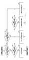
<基板処理装置1の全体構成>
まず、図1を参照しながら基板処理装置1の全体構成の一例について説明する。図1は、本実施形態に係るチャンバーコンディションの診断方法が用いられる基板処理装置1の概略構成を示す断面図である。なお、本実施形態では、基板処理装置1がスロットアンテナを用いたマイクロ波プラズマ処理装置である例について説明する。基板処理装置1のマイクロ波プラズマ処理装置は、例えば、ポリシリコンのプラズマエッチングを行う装置である。<Overall configuration of board processing device 1>
First, an example of the overall configuration of the substrate processing apparatus 1 will be described with reference to FIG. FIG. 1 is a cross-sectional view showing a schematic configuration of a substrate processing apparatus 1 in which the method for diagnosing a chamber condition according to the present embodiment is used. In this embodiment, an example in which the substrate processing device 1 is a microwave plasma processing device using a slot antenna will be described. The microwave plasma processing device of the substrate processing device 1 is, for example, a device that performs plasma etching of polysilicon.
図1に示すように、基板処理装置1は、気密に構成され、接地されたチャンバー2を備える。チャンバー2は、金属製、例えば、アルミニウム製又はステンレス鋼製である。 As shown in FIG. 1, the substrate processing apparatus 1 includes an airtightly configured and grounded
チャンバー2の内部の表面には、セラミックス溶射膜が形成されていてもよい。セラミックス溶射膜は、酸化アルミニウム、酸化イットリウム、フッ化イットリウム、オキシフッ化イットリウムのいずれかを含んでいることが好ましい。なお、チャンバー2の内部の表面を酸化アルミニウム、酸化イットリウム、フッ化イットリウム、オキシフッ化イットリウムのいずれかを含んでいる材料により形成してもよい。 A ceramic sprayed film may be formed on the inner surface of the
載置台10は、本体部8及び環状部材(エッジリング)4を含む。本体部8は、基板Wを支持するための中央領域8aと、環状部材4を支持するための環状領域8bとを有する。基板Wは、本体部8の中央領域8a上に配置され、環状部材4は、本体部8の中央領域8a上の基板Wを囲むように本体部8の環状領域8b上に配置される。本体部8は、基台及び静電チャックを含む。基台は導電性部材(下部電極)を含む。静電チャックは、基台の上に配置される。また、図示は省略するが、載置台10は、静電チャック及び基板Wのうち少なくとも1つをターゲット温度に調節するように構成される温調モジュールを含んでもよい。温調モジュールは、ヒーター、流路、又はこれらの組み合わせを含んでもよい。流路には、冷媒、伝熱ガスのような温調流体が流れる。 The mounting table 10 includes a
本体部8の下部電極は、給電棒およびマッチングユニットを介して、高周波電源21に電気的に接続されている。高周波電源21は、高周波バイアスを下部電極に供給する。高周波電源によって発生される高周波バイアスの周波数は、基板Wに引き込まれるイオンのエネルギーを制御するのに適した所定周波数、例えば、13.56MHzである。マッチングユニットは、高周波電源側のインピーダンスと、主に電極、プラズマ、チャンバー2といった負荷側のインピーダンスとの間で整合をとるための整合器22を収容している。この整合器22の中には、例えば、自己バイアス生成用のブロッキングコンデンサ等が含まれる。 The lower electrode of the
載置台10は、基板Wを支持して昇降させるための基板支持ピン(図示せず)を備える。基板支持ピンは、載置台10の表面に対して突没可能に設けられる。 The mounting table 10 includes a board support pin (not shown) for supporting and raising and lowering the board W. The board support pin is provided so as to be retractable with respect to the surface of the mounting table 10.
基板処理装置1は、チャンバー2の下部において開口する排気ポート11を備える。排気ポート11は、APC(Automatic Pressure Control)バルブ(図示しない)を介してTMP(Turbo Molecular Pump)やDP(Dry Pump)(いずれも図示しない)に接続される。TMPやDPはチャンバー2内のガス等を排気し、APCバルブはチャンバー2内の圧力を制御する。 The substrate processing device 1 includes an
チャンバー2は、側壁に、基板処理装置1に隣接する搬送室(図示せず)との間で基板Wの搬入出を行うための搬入出口25と、この搬入出口25を開閉するゲートバルブ26とを備える。 The
チャンバー2の上部は開口部となっている。基板処理装置1は、当該開口部を臨むようにマイクロ波プラズマ源20を備える。 The upper part of the
マイクロ波プラズマ源20は、アンテナ部30と、マイクロ波伝送部35と、を備える。 The
アンテナ部30は、マイクロ波透過板28と、スロットアンテナ31と、遅波材33と、を備える。 The
マイクロ波透過板28は、誘電体、例えば石英や酸化アルミニウム(Al2O3)等のセラミックスから形成される。マイクロ波透過板28は、チャンバー2の開口部を塞ぐように、チャンバー2の側壁上部に嵌め込まれる。基板処理装置1は、チャンバー2とマイクロ波透過板28との間に、シールリングを備える。シールリングを備えることにより、チャンバー2内は気密に保持される。The
スロットアンテナ31は、マイクロ波透過板28に対応する円板状の形状を有する。スロットアンテナ31は、マイクロ波透過板28に密着するように設けられる。スロットアンテナ31は、チャンバー2の側壁上端に係止される。スロットアンテナ31は導電性材料により形成される。 The
スロットアンテナ31は、例えば表面が銀若しくは金メッキされた銅板又はアルミニウム板からなる。スロットアンテナ31は、マイクロ波を放射するための複数のスロット32を備える。スロット32は、スロットアンテナ31を所定パターンで貫通するように形成される。 The
スロット32のパターンは、マイクロ波が均等に放射されるように適宜設定される。例えば、パターンの例としては、T字状に配置された2つのスロット32を一対として複数対のスロット32が同心円状に配置してもよい。スロット32の長さや配列間隔は、マイクロ波の実効波長(λg)に応じて決定される。例えばスロット32は、それらの間隔がλg/4、λg/2又はλgとなるように配置される。 The pattern of the
なお、スロット32は、円形状、円弧状等の他の形状であってもよい。さらに、スロット32の配置形態は特に限定されず、同心円状のほか、例えば、螺旋状、放射状に配置してもよい。スロット32のパターンは、所望のプラズマ密度分布が得られるマイクロ波放射特性となるように、適宜設定される。 The
遅波材33は、スロットアンテナ31の上面に密着して設けられる。遅波材33は、真空よりも大きい誘電率を有する誘電体、例えば、石英、セラミックス(Al2O3)、ポリテトラフルオロエチレン、ポリイミドなどの樹脂から形成される。遅波材33はマイクロ波の波長を真空中より短くしてスロットアンテナ31を小さくする機能を有する。The
マイクロ波透過板28及び遅波材33の厚さは、遅波材33、スロットアンテナ31、マイクロ波透過板28及びプラズマで形成される等価回路が共振条件を満たすように調整される。遅波材33の厚さを調整することにより、マイクロ波の位相を調整することができる。 The thickness of the
マイクロ波の位相を調整することにより、スロットアンテナ31の接合部が定在波の「はら」になるように厚さを調整する。また、スロットアンテナ31の接合部が定在波の「はら」になるように厚さを調整することにより、マイクロ波の反射が極小化され、マイクロ波の放射エネルギーが最大となる。さらに、遅波材33とマイクロ波透過板28を同じ材質とすることにより、マイクロ波の界面反射を防止することができる。 By adjusting the phase of the microwave, the thickness is adjusted so that the junction of the
なお、スロットアンテナ31とマイクロ波透過板28との間、また、遅波材33とスロットアンテナ31との間は、離間して配置されていてもよい。 The
アンテナ部30は、スロットアンテナ31及び遅波材33を覆うように、例えばアルミニウムやステンレス鋼、銅等の金属材からなるシールド蓋体34を備える。シールド蓋体34は、内部に形成された冷却水流路34aを備える。冷却水流路34aに冷却水を通流させることにより、シールド蓋体34は、シールド蓋体34、遅波材33、スロットアンテナ31及びマイクロ波透過板28を冷却する。なお、シールド蓋体34は接地される。 The
マイクロ波伝送部35は、同軸導波管37と、モード変換器38と、導波管39と、マイクロ波発振器40と、チューナ41と、を備える。 The
同軸導波管37は、シールド蓋体34の上壁の中央に形成された開口部36の上方から挿入される。同軸導波管37は、中空棒状の内導体37aと、円筒状の外導体37b、を備える。内導体37aと外導体37bは同心状に配置される。内導体37aと外導体37bのそれぞれは、シールド蓋体34から上方に延びている。内導体37aは、下端にテーパーコネクタ43を備える。テーパーコネクタ43は、スロットアンテナ31に接続される。テーパーコネクタ43は、先端に金属製のカバー44を備える。 The
モード変換器38は、同軸導波管37の上端に接続される。モード変換器38には、導波管39が接続される。導波管39の形状は、断面矩形状である。導波管39の一端はモード変換器38に接続され、他端はマイクロ波発振器40に接続される。 The
マイクロ波発振器40は、信号発生器45と、増幅器46と、を備える。信号発生器45は、所定の周波数の信号を増幅器46に出力する。増幅器46は、信号発生器45からの信号波形を増幅して所定パワーのマイクロ波を発振する。また、増幅器46は、周波数変調を行う。増幅器46は、例えば、中心周波数が2450MHz(2.45GHz)の場合、2400~2500MHz(2.4~2.5GHz)の間で周波数を変調可能である。なお、マイクロ波の中心周波数は2450MHzには限らず、8.35GHz、1.98GHz、860MHz、915MHz等、種々の周波数を用いることができる。 The
チューナ41は、導波管39の途中に設けられる。チューナ41は、チャンバー2内の負荷(プラズマ)のインピーダンスをマイクロ波発振器40の電源の特性インピーダンスに整合させる。 The
マイクロ波発振器40で発振されたマイクロ波は、TEモードで導波管39を伝播する。モード変換器38は、マイクロ波の伝播モードをTEモードからTEMモードに変換する。そして、モード変換器38は、TEMモードに変換されたマイクロ波を、同軸導波管37に出力する。同軸導波管37に出力されたマイクロ波は、スロットアンテナ31に導かれる。 The microwave oscillated by the
なお、モード変換器38でモード変換されてもTEモードのマイクロ波が多少残存する場合がある。TEモードのマイクロ波が残存していたとしても、同軸導波管37を介して伝播される間に残存しているTEモード成分のマイクロ波はTEMモードに変換される。 Even if the mode is converted by the
同軸導波管37の内導体37aは、中央部に、上部からテーパーコネクタ43に至る孔47を有する。孔47には、温度検出器として第1熱電対51がテーパーコネクタ43の位置まで挿入される。第1熱電対51によりアンテナ部30の中央部の温度が検出される。一方、シールド蓋体34の端部には、温度検出器として第2熱電対52が設けられる。第2熱電対52によりアンテナ部30の端部の温度が検出される。 The
第1熱電対51で検出されたアンテナ部中央の温度(Tcent)の信号及び第2熱電対52で検出されたアンテナ部端部の温度(Tedge)の信号は、マイクロ波の周波数を制御する周波数制御器50に入力される。第1熱電対51及び第2熱電対52は、いずれもアンテナ部30の外部から挿入され、大気部分に配置される。 The temperature (Tcent) signal at the center of the antenna portion detected by the
周波数制御器50は、第1熱電対51で検出された温度Tcent及び第2熱電対52で検出された温度Tedgeに基づいて、プラズマの密度分布が最適化されるように、マイクロ波発振器40に指令を与える。マイクロ波発振器40は、周波数制御器50から指令に基づいて、出力するマイクロ波の発振周波数を制御する。 The
温度Tcent及び温度Tedgeは、それぞれチャンバー2内のマイクロ波透過板28下面の中央部及びエッジ部の温度と相関がある。また、マイクロ波の発振周波数を変動させることによりスロットアンテナ31から放射する電界の分布を操作して、プラズマ密度分布を高精度に制御できる。 The temperature Tcent and the temperature Tedge correlate with the temperature of the central portion and the edge portion of the lower surface of the
マイクロ波プラズマ源20は、同軸導波管37の下部に、複数のスタブ部材42を備える。スタブ部材42は、周方向に複数設けられる。スタブ部材42のそれぞれは、外導体37bから内導体37aへ向かって延出可能になっている。スタブ部材42は、その先端と内導体37aとの距離を調節することにより、マイクロ波の伝搬を周方向に調節できる。 The
基板処理装置1は、さらに、チャンバー2の側壁を介してチャンバー2内にガスを供給するガス供給部60を備える。ガス供給部60は、ガス供給源61と、配管62と、バッファ室63と、ガス流路64と、ガス吐出口65と、を備える。 The substrate processing device 1 further includes a
ガス供給源61は、プラズマ処理に応じて適切なガスを供給する。配管62は、ガス供給源61とチャンバー2とを接続する。配管62は、ガス供給源61からチャンバー2までの間に設けられる。バッファ室63は、チャンバー2の側壁に沿って環状に設けられる。ガス流路64は、配管62とバッファ室63とを接続する。ガス吐出口65は、バッファ室63から等間隔でチャンバー2内に臨むように水平に複数設けられる。 The
ガス供給部60からは、プラズマ処理に応じて適切なガスが供給されるようになっている。プラズマ処理としてはポリシリコンエッチング処理が例示され、その際の処理ガスとしては、例えば、塩素ガス(Cl2ガス)、臭化水素ガス(HBrガス)及び三フッ化窒素ガス(NF3ガス)等のガスやヘリウムガス(Heガス)等の不活性ガスが供給される。An appropriate gas is supplied from the
ガス供給源61はガスの数(ガスの種類)に応じて複数設けられる。それぞれのガス供給源61から配管62が延びている。配管62にはバルブ及びマスフローコントローラ等の流量制御器(いずれも図示せず)が設けられる。 A plurality of
チャンバー2の側壁には、ガラス窓55を備える。ガラス窓55に対向する位置に、分光器56を備える。分光器56は、ガラス窓55を通過してチャンバー2の内部のプラズマから放射される光を受光する。そして、分光器56は、受光した光から特定の波長の発光強度(分光強度)を測定する。 A
基板処理装置1は、制御部70を備える。制御部70は、基板処理装置1の各構成部、例えばマイクロ波発振器40、ガス供給部60のバルブ、分光器56及び流量制御器等を制御する。制御部70は、CPU(Central Processing Unit)(コンピュータ)を有する主制御部と、入力装置(キーボード、マウス等)、出力装置(プリンタ等)、表示装置(ディスプレイ等)、記憶装置(記憶媒体)を備える。 The substrate processing device 1 includes a
記憶装置には、基板処理装置1で実行される各種処理のパラメータが記憶される。また、記憶装置は、基板処理装置1で実行される処理を制御するためのプログラム、すなわち処理レシピが格納された記憶媒体がセットされる。主制御部は、記憶媒体に記憶されている所定の処理レシピを呼び出し、その処理レシピに基づいて基板処理装置1により所定の処理が行われるように制御する。 The storage device stores parameters of various processes executed by the board processing device 1. Further, the storage device is set with a program for controlling the processing executed by the substrate processing device 1, that is, a storage medium in which the processing recipe is stored. The main control unit calls a predetermined processing recipe stored in the storage medium, and controls the substrate processing apparatus 1 to perform the predetermined processing based on the processing recipe.
基板処理装置1では、まずゲートバルブ26を開状態にして加工対象の基板Wをチャンバー2内に搬入し、載置台10の上に載置する。そして、基板処理装置1では、ガス供給部60より処理ガス(例えば、Cl2ガス、HBrガス等)を所定の流量及び流量比でチャンバー2内に導入し、APCバルブによりチャンバー2内の圧力を所定値にする。In the substrate processing apparatus 1, first, the
さらに、基板処理装置1では、マイクロ波発振器40からマイクロ波をチャンバー2に供給する。また、高周波電源21から載置台に高周波電力を供給する。ガス吐出口65より吐出された処理ガスはプラズマ化され、プラズマ中のラジカルやイオンによって基板Wがエッチング処理される。 Further, in the substrate processing apparatus 1, microwaves are supplied to the
<チャンバーコンディションの診断方法>
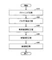
基板処理装置1のチャンバー2のコンディション(チャンバーコンディション)を診断する方法について説明する。図2は、本実施形態に係るチャンバーコンディションの診断方法のフローチャートである。<Diagnosis method of chamber condition>
A method of diagnosing the condition (chamber condition) of the
本実施形態のチャンバーコンディションの診断方法は、チャンバーの内面に起因するフッ素に着目して、チャンバーのコンディションを診断する。チャンバーの内面に起因するフッ素とは、処理ガスに含まれるフッ素がチャンバー内面を形成する溶射膜上に付着したものや溶射膜中に入り込んだもの、あるいは、溶射膜自体に元々含まれるフッ素のことを言う。チャンバーの内面に起因するフッ素量は、チャンバーコンディションに影響を与える。本実施形態のチャンバーコンディションの診断方法は、ヘリウムガスを用いてプラズマを発生させた際のフッ素の発光強度(分光強度)により、チャンバーのコンディションを診断する。 In the method for diagnosing the chamber condition of the present embodiment, the condition of the chamber is diagnosed by focusing on the fluorine generated from the inner surface of the chamber. Fluorine caused by the inner surface of the chamber means that the fluorine contained in the processing gas adheres to the sprayed film forming the inner surface of the chamber, enters the sprayed film, or is originally contained in the sprayed film itself. Say. The amount of fluorine resulting from the inner surface of the chamber affects the condition of the chamber. In the method for diagnosing the chamber condition of the present embodiment, the condition of the chamber is diagnosed by the emission intensity (spectral intensity) of fluorine when plasma is generated using helium gas.
(ステップS10)
最初に、制御部70は、チャンバー2の内部をクリーニングするクリーニング工程を行う。クリーニング工程では、例えば、基板処理を行った際にチャンバー2の内部に付着したフッ素等を除去する。チャンバー2の内部をクリーニングすることによって、チャンバー内部を初期状態にする。(Step S10)
First, the
(ステップS20)
次に、制御部70は、チャンバー2の内部に、ヘリウムガスを含み、アルゴンガスを含まない1種類以上の不活性ガスのプラズマを生成するプラズマ生成工程を行う。いいかえると、チャンバー2の内部に、ヘリウムガス、又は、ヘリウムガスにアルゴンガスを含まない1種類以上の不活性ガスを混合させたガスのプラズマを生成するプラズマ生成工程を行う。(Step S20)
Next, the
プラズマ生成工程において、本体部8の中央領域8a上に、例えば、シリコンで形成された製品基板とは異なるダミー基板が載置されてもよい。そして、制御部70は、ガス供給部60から、ヘリウムガスを含み、アルゴンガスを含まない1種類以上の不活性ガスをチャンバー2の内部に供給するように制御する。チャンバー2にヘリウムガスを含み、アルゴンガスを含まない1種類以上の不活性ガスが供給された状態で、制御部70は、マイクロ波発振器40からマイクロ波をチャンバー2に供給し、高周波電源21から載置台に高周波電力を供給するように制御する。 In the plasma generation step, for example, a dummy substrate different from the product substrate made of silicon may be placed on the
上記のようにして、チャンバー2の内部に、ヘリウムガスを含み、アルゴンガスを含まない1種類以上の不活性ガスのプラズマが生成される。いいかえると、ヘリウムガス、又は、ヘリウムガスにアルゴンガスを含まない1種類以上の不活性ガスを混合させたガスのプラズマが生成される。 As described above, plasma of one or more kinds of inert gas containing helium gas and not containing argon gas is generated inside the
本実施形態のチャンバーコンディションの診断方法では、プラズマを生成するのにヘリウムガスを含み、アルゴンガスを含まない1種類以上の不活性ガスが用いられる。ヘリウムガスが用いられるのは、後述するように、プラズマが発生してから安定するまでの時間が短いからである。また、アルゴンと比較すると、スパッタレートが小さく、チャンバーへのダメージを小さくするためである。 In the method for diagnosing the chamber condition of the present embodiment, one or more kinds of inert gases containing helium gas and not argon gas are used to generate plasma. Helium gas is used because, as will be described later, the time from plasma generation to stabilization is short. Further, the sputter rate is smaller than that of argon, and the damage to the chamber is reduced.
なお、アルゴンの発光波長は、フッ素の発光波長と重複する部分が多いため、混合ガスの場合はアルゴンを除く不活性ガスを用いる。当該不活性ガスの例としては、例えば、キセノンガス、ネオンガス、クリプトンガス等である。ヘリウムガスを含み、アルゴンガスを含まない1種類以上の不活性ガスは、例えば、ヘリウムガス単体でもよいし、ヘリウムガスとキセノンガス、ネオンガス、クリプトンガス等のアルゴンガスを除く不活性ガスとの混合ガスでもよい。 Since the emission wavelength of argon often overlaps with the emission wavelength of fluorine, an inert gas other than argon is used in the case of a mixed gas. Examples of the inert gas are, for example, xenon gas, neon gas, krypton gas and the like. The one or more kinds of inert gas containing helium gas and not containing argon gas may be, for example, helium gas alone, or a mixture of helium gas and an inert gas other than argon gas such as xenon gas, neon gas, and krypton gas. It may be gas.
(ステップS30)
次に、制御部70は、前記チャンバーの内部のフッ素の発光強度を測定する発光強度測定工程を行う。制御部70は、分光器56が、チャンバー2の内部のプラズマの発光強度を測定するように制御する。具体的には、制御部70は、分光器56がフッ素の発光強度を測定するように制御する。例えば、制御部70は、フッ素の発光波長である686nmにおける発光強度を測定するように分光器56を制御する。(Step S30)
Next, the
(ステップS40)
次に、制御部70は、ステップS30で測定した発光強度に基づいて、チャンバー2の状態(チャンバーコンディション)について診断を行う。(Step S40)
Next, the
例えば、ステップS30で測定したフッ素の発光強度が、第1閾値以上であって、第1閾値より大きい第2閾値以下である場合は、制御部70は、チャンバー2内の状態(チャンバーコンディション)は正常な状態(正常状態)である、と判断する。 For example, when the emission intensity of fluorine measured in step S30 is equal to or higher than the first threshold value and equal to or lower than the second threshold value larger than the first threshold value, the
また、ステップS30で測定したフッ素の発光強度が第1閾値未満である場合は、制御部70は、チャンバー2内の状態(チャンバーコンディション)はチャンバー2の内面のフッ素が不足している状態(フッ素不足状態)であると診断する。 When the emission intensity of fluorine measured in step S30 is less than the first threshold value, the
さらに、ステップS30で測定したフッ素の発光強度が第2閾値より大きい場合は、制御部70は、チャンバー2内の状態(チャンバーコンディション)は、チャンバー2の内面のフッ素が過剰に存在している状態(フッ素過剰状態)であると診断する。 Further, when the emission intensity of fluorine measured in step S30 is larger than the second threshold value, the
さらにまた、ステップS30で測定したフッ素の発光強度が第1閾値より小さい第3閾値未満である場合、又は、当該発光強度が第2閾値より大きい第4閾値より大きいと診断した場合は、チャンバー2内の状態(チャンバーコンディション)はチャンバー2の内の部品が劣化しており、当該部品の交換が必要な状態(部品劣化状態)であると診断する。 Furthermore, when the emission intensity of fluorine measured in step S30 is less than the third threshold value smaller than the first threshold value, or when it is diagnosed that the emission intensity is larger than the fourth threshold value larger than the second threshold value, the
具体的な処理の流れについて説明する。図3は、本実施形態に係るチャンバーコンディションの診断方法のフローチャートである。具体的には、ステップS40の状態推定工程のフローチャートである。 A specific processing flow will be described. FIG. 3 is a flowchart of a method for diagnosing a chamber condition according to the present embodiment. Specifically, it is a flowchart of the state estimation process of step S40.
最初に、ステップS41において、制御部70は、ステップS30で測定したフッ素の発光強度が第1閾値以上であるか判定を行う。ステップS30で測定したフッ素の発光強度が第1閾値以上である場合(ステップS41のYes)は、制御部70は、ステップS30で測定したフッ素の発光強度が第1閾値より大きい値である第2閾値以下であるか判定を行う(ステップS42)。ステップS30で測定したフッ素の発光強度が第1閾値より大きい第2閾値以下である場合(ステップS42のYes)は、制御部70は、基板処理装置1のチャンバー2の状態(チャンバーコンディション)は、正常状態であると推定する(ステップS43)。 First, in step S41, the
ステップS41において、ステップS30で測定したフッ素の発光強度が第1閾値未満の場合(ステップS41のNo)は、制御部70は、ステップS30で測定したフッ素の発光強度が第1閾値より小さい値である第3閾値以上であるか判定を行う(ステップS44)。ステップS30で測定したフッ素の発光強度が第3閾値以上である場合(ステップS44のYes)は、制御部70は、基板処理装置1のチャンバー2の状態(チャンバーコンディション)は、フッ素不足状態であると推定する(ステップS45)。 In step S41, when the emission intensity of fluorine measured in step S30 is less than the first threshold value (No in step S41), the
ステップS42において、ステップS30で測定したフッ素の発光強度が第2閾値より大きい場合(ステップS42のNo)は、制御部70は、ステップS30で測定したフッ素の発光強度が第2閾値より大きい値である第4閾値以下であるか判定を行う(ステップS46)。ステップS30で測定したフッ素の発光強度が第4閾値以下である場合(ステップS46のYes)は、制御部70は、基板処理装置1のチャンバー2の状態(チャンバーコンディション)は、フッ素過剰状態であると推定する(ステップS47)。 In step S42, when the emission intensity of fluorine measured in step S30 is larger than the second threshold value (No in step S42), the
ステップS44において、ステップS30で測定したフッ素の発光強度が第3閾値未満である場合(ステップS44のNo)は、制御部70は、基板処理装置1のチャンバー2の状態(チャンバーコンディション)は、部品劣化状態であると推定する(ステップS48)。また、ステップS46において、ステップS30で測定したフッ素の発光強度が第4閾値より大きい場合(ステップS46のNo)は、制御部70は、基板処理装置1のチャンバー2の状態(チャンバーコンディション)は、部品劣化状態であると推定する(ステップS48)。部品劣化状態では、後述する後処理工程のステップS53、ステップS54の処理を行っても、正常状態にならないと判断して、部品の交換を行うよう指示する。 In step S44, when the emission intensity of fluorine measured in step S30 is less than the third threshold value (No in step S44), the
また、例えば、ステップS30で測定したフッ素の発光強度から後述するように、基板Wをエッチングする際のポリシリコンエッチングレートを推定して、制御部70は、チャンバー2の状態が所望のポリシリコンエッチングレートでエッチングできる状態であるかを推定してもよい。 Further, for example, as will be described later from the emission intensity of fluorine measured in step S30, the polysilicon etching rate at the time of etching the substrate W is estimated, and the
(ステップS50)
次に、制御部70は、ステップS40における診断結果に基づいて、後処理工程を行う。ステップS50の処理の詳細について説明する。図4は、本実施形態に係るチャンバーコンディションの診断方法のフローチャートである。具体的には、図4は、ステップS50の後処理工程のフローチャートである。(Step S50)
Next, the
ステップS50の後処理工程では、ステップS51において、制御部70は、ステップS40の状態推定工程の推定結果に基づいて、処理を行う。 In the post-processing step of step S50, in step S51, the
ステップS51で、ステップS40の状態推定工程で、正常状態であると推定された場合(ステップS51の「正常状態」)は、特に後処理工程において処理を行わず(ステップS52)に、後処理工程を終了する。 In step S51, when it is estimated to be in a normal state in the state estimation step of step S40 (“normal state” in step S51), no processing is particularly performed in the post-processing step (step S52), and the post-processing step is performed. To finish.
ステップS51で、ステップS40の状態推定工程で、フッ素不足状態であると推定された場合(ステップS51の「フッ素不足状態」)は、制御部70は、フッ素を含むガスによるプラズマ処理を行うように制御する(ステップS53)。フッ素を含むガスによるプラズマ処理を行い、例えば、溶射膜上にフッ素を付着させあるいは溶射膜中にフッ素を入れ込み、あるいは、溶射膜をフッ化させることでチャンバー内面のフッ素量を増やす。
フッ素を含むガスは、例えば、CF4ガスやNF3ガスを含むガスであるがこれに限らない。当該プラズマ処理が終了したら制御部70は、後処理工程を終了する。In step S51, when it is estimated in the state estimation step of step S40 that the fluorine is deficient (“fluorine deficient state” in step S51), the
The gas containing fluorine is, for example, a gas containing CF4 gas and NF3 gas, but is not limited to this. When the plasma processing is completed, the
ステップS51で、ステップS40の状態推定工程で、フッ素過剰状態であると推定された場合(ステップS51の「フッ素過剰状態」)は、制御部70は、酸素を含むガスによるプラズマ処理を行うように制御する(ステップS54)。酸素を含むガスによるプラズマ処理を行い、例えば、溶射膜を酸化させることでチャンバー内面のフッ素量を相対的に低下させる。酸素を含むガスは、例えば、O2ガスを含むガスであるがこれに限らない。当該プラズマ処理が終了したら制御部70は、後処理工程を終了する。In step S51, when it is estimated in the state estimation step of step S40 that the fluorine is in excess (“fluorine excess state” in step S51), the
ステップS51で、ステップS40の状態推定工程で、部品劣化状態であると推定された場合(ステップS51の「部品劣化状態」)は、制御部70は、部品交換を行うように表示(指示)を行う(ステップS55)。当該表示処理が終了したら制御部70は、後処理工程を終了する。 In step S51, when it is estimated in the state estimation step of step S40 that the parts are in a deteriorated state (“parts deteriorated state” in step S51), the
なお、本実施形態のチャンバーコンディションの診断方法は、例えば、基板処理装置1の装置立ち上げ後、基板処理装置1の装置メンテナンス後又は基板処理装置1において製品基板処理前後に実施される。 The method for diagnosing the chamber condition of the present embodiment is carried out, for example, after the apparatus of the substrate processing apparatus 1 is started up, after the equipment maintenance of the substrate processing apparatus 1, or before and after the product substrate processing in the substrate processing apparatus 1.
[チャンバーコンディションの診断方法が用いられる装置診断]
次に、本実施形態のチャンバーコンディションの診断方法が用いられる装置診断について説明する。図5は、本実施形態に係るチャンバーコンディションの診断方法が用いられる装置診断の時間軸に対する概念図である。[Device diagnosis using the method of diagnosing chamber conditions]
Next, an apparatus diagnosis using the method for diagnosing the chamber condition of the present embodiment will be described. FIG. 5 is a conceptual diagram with respect to the time axis of device diagnosis in which the chamber condition diagnosis method according to the present embodiment is used.
図5の中心から左側は、装置を立ち上げる際の工程を示す。図5の中心から右側は、装置を立ち上げてから基板の処理(基板処理)を行う工程を示す。なお、時間軸は左から右に経過する。 The left side from the center of FIG. 5 shows a process for starting up the device. The right side from the center of FIG. 5 shows a process of starting up the apparatus and then processing the substrate (board processing). The time axis elapses from left to right.
装置を立ち上げる際には、部品の組み付けあるいは部品交換等のメンテナンスを行った後、真空引きを行いながらチャンバー内の温度を上昇させる。そして、チャンバーのリークがないかチェックを行い、チャンバーの状態のチェック(ヘルスチェック)を行う。そして、コンディショニング処理を行う。上記の工程により、部品等の組み付けの正常性を確認したり、大気リークの有無をチェックしたり、デガスや水分の有無をチェックしたりする。また、コンディショニングを行うことにより、チャンバー内面の酸化、フッ化を行ったり、必要な膜等を堆積(デポ)したりする。装置を立ち上げることによって、チャンバー内部の状態を初期状態にする。 When starting up the device, after performing maintenance such as assembling parts or replacing parts, the temperature inside the chamber is raised while evacuating. Then, it is checked whether there is a leak in the chamber, and the state of the chamber is checked (health check). Then, the conditioning process is performed. Through the above process, the normality of assembly of parts and the like is confirmed, the presence or absence of atmospheric leaks is checked, and the presence or absence of degas and moisture is checked. In addition, by performing conditioning, oxidation and fluoride of the inner surface of the chamber are performed, and necessary membranes and the like are deposited (depot). By starting up the device, the state inside the chamber is reset to the initial state.
そして、最後に、基板処理装置の品質を調査するため、載置台に装置状態の正常性を判定するためのQC(quality control)基板を載置してポリシリコンエッチングレートの測定を行う。また、載置台にダミー基板を載置して基準となる発光データを取得する。なお、基準となる発光データの測定条件は、例えば、チャンバー圧力80mT、マイクロ波(2.45GHz)2000W、高周波電力 100W、He=300sccm、30secである。ポリシリコンエッチングレートの測定条件は、例えば、チャンバー圧力120mT、マイクロ波(2.45GHz)2000W、高周波電力 300W、HBr/O2/He=800/6/1000sccm、60secである。 Finally, in order to investigate the quality of the substrate processing apparatus, a QC (quality control) substrate for determining the normality of the apparatus state is placed on the mounting table, and the polysilicon etching rate is measured. In addition, a dummy substrate is placed on the mounting table to acquire reference light emission data. The measurement conditions of the reference light emission data are, for example, a chamber pressure of 80 mT, a microwave (2.45 GHz) 2000 W, a high frequency power of 100 W, He = 300 sccm, and 30 sec. The measurement conditions of the polysilicon etching rate are, for example, a chamber pressure of 120 mT, a microwave (2.45 GHz) of 2000 W, a high frequency power of 300 W, HBr / O2 / He = 800/6/1000 sccm, and 60 sec.
次に、実際の基板処理を行う。基板処理を行いながら、一定の時間間隔で載置台にQC基板を載置してポリシリコンエッチングレートを測定する。一定の時間間隔でポリシリコンエッチングレートを測定することにより、例えば、0時間から200時間の処理時間の間で所定の間隔でポリシリコンエッチングレートの変動データ(ポリシリコンエッチングレート変動)を取得する。また、ポリシリコンエッチングレートの測定の直前又は直後に、載置台にダミー基板を載置して所定の波長、本実施形態ではフッ素の発光波長の発光データを取得する。フッ素の発光データを取得することによって、例えば、0時間から200時間の処理時間の間で所定の間隔で分光器により発光データの変動データ(分光器発光データ変動)を取得する。図5では、例として、フッ素の発光データが時間の経過とともに小さくなっていることを模式的に示している。分光器発光データ変動を取得することによって、チャンバーのバックグランドの発光データ(チャンバーバックグラウンド)を数値化する。 Next, the actual substrate processing is performed. While processing the substrate, the QC substrate is placed on the mounting table at regular time intervals and the polysilicon etching rate is measured. By measuring the polysilicon etching rate at regular time intervals, for example, the polysilicon etching rate fluctuation data (polysilicon etching rate fluctuation) is acquired at predetermined intervals between the processing times of 0 hours to 200 hours. Further, immediately before or immediately after the measurement of the polysilicon etching rate, a dummy substrate is placed on a mounting table to acquire emission data of a predetermined wavelength, that is, a emission wavelength of fluorine in the present embodiment. By acquiring the emission data of fluorine, for example, fluctuation data of emission data (variation of emission data of the spectroscope) is acquired by a spectroscope at predetermined intervals between 0 hours and 200 hours of processing time. In FIG. 5, as an example, it is schematically shown that the emission data of fluorine becomes smaller with the passage of time. The emission data (chamber background) of the background of the chamber is quantified by acquiring the fluctuation of the emission data of the spectroscope.
なお、一度、ポリシリコンエッチングレート変動と分光器発光データ変動を取得した後は、取得した分光器発光データからポリシリコンエッチングレートを推定することができる。すなわち、QC基板によるポリシリコンエッチングレートの測定を省略することができる。即ち、QC基板の使用を省略することができる。また、QC基板を使用しないため、コストを抑えることができ、さらに、装置診断、例えば、装置の正常安定性の診断を効率よく行うことができる。装置診断の効率化によって、装置を用いる基板処理の生産性を向上させることができる。 Once the polysilicon etching rate fluctuation and the spectroscope emission data fluctuation are acquired, the polysilicon etching rate can be estimated from the acquired spectroscope emission data. That is, the measurement of the polysilicon etching rate by the QC substrate can be omitted. That is, the use of the QC board can be omitted. Further, since the QC board is not used, the cost can be suppressed, and the device diagnosis, for example, the normal stability diagnosis of the device can be efficiently performed. By improving the efficiency of device diagnosis, it is possible to improve the productivity of substrate processing using the device.
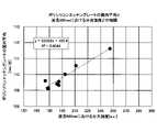
実際に測定を行った結果について説明する。図6は、本実施形態に係るチャンバーコンディションの診断方法が用いられる発光強度の時系列データを示す図である。図7は、本実施形態に係るチャンバーコンディションの診断方法が用いられるポリシリコンエッチングレートの面内平均の時系列データを示す図である。ポリシリコンエッチングレートは、フッ素を含むガスのプラズマを用いてQC基板をエッチングしたときのポリシリコンエッチングレートである。 The results of actual measurements will be described. FIG. 6 is a diagram showing time-series data of luminescence intensity in which the method for diagnosing a chamber condition according to the present embodiment is used. FIG. 7 is a diagram showing time-series data of the in-plane average of the polysilicon etching rate in which the method for diagnosing the chamber condition according to the present embodiment is used. The polysilicon etching rate is the polysilicon etching rate when the QC substrate is etched using plasma of a gas containing fluorine.
図6の横軸は、基板処理装置1において、高周波電力を印加した積算時間を表す。図6の縦軸は、波長686nmにおける発光強度である。波長686nmは、フッ素の発光波長である。したがって、図6の縦軸は、フッ素の発光強度を表す。なお、波長686nmにおける発光強度は、高周波電力の印加を開始してから、すなわち、プラズマを発生させてから、25秒後の発光強度(3秒間の平均値)である。図7の横軸は、基板処理装置1において、高周波電力を印加した積算時間を表す。図7の縦軸は、ポリシリコンエッチングレートの面内平均である。 The horizontal axis of FIG. 6 represents the integration time when high frequency power is applied in the substrate processing device 1. The vertical axis of FIG. 6 is the emission intensity at a wavelength of 686 nm. The wavelength of 686 nm is the emission wavelength of fluorine. Therefore, the vertical axis of FIG. 6 represents the emission intensity of fluorine. The emission intensity at a wavelength of 686 nm is the emission intensity (average value for 3 seconds) 25 seconds after the application of high-frequency power is started, that is, after the plasma is generated. The horizontal axis of FIG. 7 represents the integrated time when high frequency power is applied in the substrate processing device 1. The vertical axis of FIG. 7 is the in-plane average of the polysilicon etching rate.
図6、図7より、高周波電力の印加時間が長くなると、ポリシリコンエッチングレート及びフッ素の発光強度(分光強度)は小さくなる。ここで、ポリシリコンエッチングレートとフッ素の発光強度(分光強度)と相関関係について説明する。図8は、本実施形態に係るチャンバーコンディションの診断方法が用いられるポリシリコンエッチングレートの面内平均と発光強度の相関を示す図である。 From FIGS. 6 and 7, as the application time of high frequency power becomes longer, the polysilicon etching rate and the emission intensity (spectral intensity) of fluorine become smaller. Here, the correlation between the polysilicon etching rate and the emission intensity (spectral intensity) of fluorine will be described. FIG. 8 is a diagram showing the correlation between the in-plane average of the polysilicon etching rate and the emission intensity in which the method for diagnosing the chamber condition according to the present embodiment is used.
図8の結果より、ポリシリコンエッチングレートとフッ素の発光波長の発光強度(分光強度)との間には、相関関係があることが分かる。すなわち、ポリシリコンエッチングレートとフッ素の発光波長の発光強度(分光強度)のいずれか一方を求めることにより、他方を推定することができる。例えば、フッ素の発光強度(分光強度)を測定することにより、ポリシリコンエッチングレートを推定することができる。 From the results of FIG. 8, it can be seen that there is a correlation between the polysilicon etching rate and the emission intensity (spectral intensity) of the emission wavelength of fluorine. That is, the other can be estimated by obtaining either the polysilicon etching rate or the emission intensity (spectral intensity) of the emission wavelength of fluorine. For example, the polysilicon etching rate can be estimated by measuring the emission intensity (spectral intensity) of fluorine.
[ヘリウムガスを用いたプラズマ処理について]
本実施形態において、フッ素の発光強度(分光強度)を測定する際に、ヘリウムガスを用いる。ヘリウムガスの用いたプラズマ処理について説明する。図9は、生成したプラズマと、所定の波長の発光強度の関係を示す図である。図9の横軸は、高周波電力を印加してから、すなわち、プラズマを発生させてからの時間を表す。図9の縦軸は、波長288.5nmの発光強度を表す。波長288.5nmは、シリコン又は一酸化炭素の発光波長である。ラインL_Heは、ヘリウムガスを用いたプラズマ処理における波長288.5nmの発光強度である。ラインL_Arは、アルゴンガスを用いたプラズマ処理における波長288.5nmの発光強度である。[Plasma treatment using helium gas]
In this embodiment, helium gas is used when measuring the emission intensity (spectral intensity) of fluorine. Plasma treatment using helium gas will be described. FIG. 9 is a diagram showing the relationship between the generated plasma and the emission intensity of a predetermined wavelength. The horizontal axis of FIG. 9 represents the time after applying high frequency power, that is, after generating plasma. The vertical axis of FIG. 9 represents the emission intensity at a wavelength of 288.5 nm. The wavelength 288.5 nm is the emission wavelength of silicon or carbon monoxide. The line L_He has an emission intensity of 288.5 nm in wavelength in plasma treatment using helium gas. Line L_Ar is the emission intensity at a wavelength of 288.5 nm in plasma treatment using argon gas.
ラインL_HeとラインL_Arとを比較すると、ヘリウムガスを用いたプラズマ処理における発光強度の方がアルゴンガスを用いたプラズマ処理における発光強度より早く収束する。例えば、ヘリウムガスを用いたプラズマ処理における発光強度は、1秒程度経過すると安定する。一方、アルゴンガスを用いたプラズマ処理における発光強度は、安定するのに10秒以上かかっている。したがって、ヘリウムガスを用いたプラズマ処理の方が、プラズマを発生させてからすぐに安定した発光強度を取得することができ、測定時間(診断時間)を短くすることができる。 Comparing the line L_He and the line L_Ar, the emission intensity in the plasma treatment using helium gas converges faster than the emission intensity in the plasma treatment using argon gas. For example, the emission intensity in plasma treatment using helium gas stabilizes after about 1 second. On the other hand, the emission intensity in the plasma treatment using argon gas takes 10 seconds or more to stabilize. Therefore, in the plasma treatment using helium gas, stable emission intensity can be obtained immediately after the plasma is generated, and the measurement time (diagnosis time) can be shortened.
図10は、生成したプラズマと、所定の波長の発光強度の関係を示す図である。図10の横軸は、高周波電力を印加してから、すなわち、プラズマを発生させてからの時間を表す。図10の縦軸は、波長686nmの発光強度を表す。波長686nmは、フッ素の発光波長である。ラインL_Heは、ヘリウムガスを用いたプラズマ処理における波長686nmの発光強度である。波長686nmの発光強度においても、ヘリウムガスを用いたプラズマ処理における発光強度は、プラズマを発光させてから1秒程度経過すると安定している。このように、ヘリウムガスを用いたプラズマ処理における発光強度は早く収束する。なお、アルゴンガスを用いたプラズマ処理を行った場合には、アルゴンガス自体が波長686nmにピークを有している。アルゴンガス自体が波長686nmにピークを有しているため、フッ素による発光強度を測定することができない。 FIG. 10 is a diagram showing the relationship between the generated plasma and the emission intensity of a predetermined wavelength. The horizontal axis of FIG. 10 represents the time after applying high frequency power, that is, after generating plasma. The vertical axis of FIG. 10 represents the emission intensity at a wavelength of 686 nm. The wavelength of 686 nm is the emission wavelength of fluorine. Line L_He is the emission intensity at a wavelength of 686 nm in plasma treatment using helium gas. Even at the emission intensity of 686 nm, the emission intensity in the plasma treatment using helium gas is stable about 1 second after the plasma is emitted. In this way, the emission intensity in the plasma treatment using helium gas converges quickly. When plasma treatment using argon gas is performed, the argon gas itself has a peak at a wavelength of 686 nm. Since the argon gas itself has a peak at a wavelength of 686 nm, the emission intensity due to fluorine cannot be measured.
次に、条件を変えて測定した結果を示す。図11は、本実施形態に係るチャンバーコンディションの診断方法が用いられる発光強度の時系列データを示す図である。図12は、本実施形態に係るチャンバーコンディションの診断方法が用いられるポリシリコンエッチングレートの面内平均と発光強度の相関を示す図である。 Next, the results of measurement under different conditions are shown. FIG. 11 is a diagram showing time-series data of luminescence intensity in which the method for diagnosing a chamber condition according to the present embodiment is used. FIG. 12 is a diagram showing the correlation between the in-plane average of the polysilicon etching rate and the emission intensity in which the method for diagnosing the chamber condition according to the present embodiment is used.
図11の横軸は、基板処理装置1において、高周波電力を印加した積算時間を表す。図11の縦軸は、波長686nmにおける発光強度である。波長686nmは、フッ素の発光波長である。したがって、図11の縦軸は、フッ素の発光強度を表す。なお、波長686nmにおける発光強度は、高周波電力の印加を開始してから、すなわち、プラズマを発生させてから、9秒後の発光強度(3秒間の平均値)である。 The horizontal axis of FIG. 11 represents the integration time when high frequency power is applied in the substrate processing device 1. The vertical axis of FIG. 11 is the emission intensity at a wavelength of 686 nm. The wavelength of 686 nm is the emission wavelength of fluorine. Therefore, the vertical axis of FIG. 11 represents the emission intensity of fluorine. The emission intensity at a wavelength of 686 nm is the emission intensity (average value for 3 seconds) 9 seconds after the application of high-frequency power is started, that is, after the plasma is generated.
図12より、プラズマを発生させてからの発光強度を測定するまでの時間が短くても、ポリシリコンエッチングレートとフッ素の発光波長の発光強度(分光強度)との相関があることが分かる。すなわち、プラズマを発生させてからの発光強度を測定するまでの時間が短くても、発光強度を測定することによって、ポリシリコンエッチングレートを推定できる。さらに、診断にかかる時間を短くすることができ診断効率を上げることができる。 From FIG. 12, it can be seen that there is a correlation between the polysilicon etching rate and the emission intensity (spectral intensity) of the emission wavelength of fluorine even if the time from the generation of plasma to the measurement of the emission intensity is short. That is, even if the time from the generation of plasma to the measurement of the emission intensity is short, the polysilicon etching rate can be estimated by measuring the emission intensity. Further, the time required for diagnosis can be shortened and the diagnosis efficiency can be improved.
今回開示された本実施形態に係る基板処理装置のチャンバーコンディションの診断方法は、すべての点において例示であって制限的なものではないと考えられるべきである。上記の実施形態は、添付の請求の範囲及びその主旨を逸脱することなく、様々な形態で変形及び改良が可能である。上記複数の実施形態に記載された事項は、矛盾しない範囲で他の構成も取り得ることができ、また、矛盾しない範囲で組み合わせることができる。 It should be considered that the method for diagnosing the chamber condition of the substrate processing apparatus according to the present embodiment disclosed this time is exemplary in all respects and is not restrictive. The above embodiment can be modified and improved in various forms without departing from the scope of the attached claims and the gist thereof. The matters described in the plurality of embodiments may have other configurations within a consistent range, and may be combined within a consistent range.
本開示の基板処理装置のチャンバーコンディションの診断方法は、マイクロ波によるプラズマ生成する装置を例に挙げて説明したが、これに限らない。Capacitively Coupled Plasma(CCP)、Inductively Coupled Plasma(ICP)、Electron Cyclotron Resonance Plasma(ECR)、そしてHelicon Wave Plasma(HWP)などのどのタイプでも適用可能である。 The method for diagnosing the chamber condition of the substrate processing apparatus of the present disclosure has been described by exemplifying an apparatus that generates plasma by microwaves, but the present invention is not limited to this. Capacitively Coupled Plasma (CCP), Inductively Coupled Plasma (ICP), Electron Cyclotron Resonance Plasma (ECR), and any type of Plasma that can be applied to Helicon Wave (ECR).
1 基板処理装置
2 チャンバー
S10、S20、S30、S40、S50 ステップ
W 基板1
Claims (10)
Translated fromJapanese前記チャンバーの内部をクリーニングする工程と、
前記チャンバーの内部に、ヘリウムガス、又は、ヘリウムガスにアルゴンガスを含まない1種類以上の不活性ガスを混合させたガスのプラズマを生成する工程と、
前記チャンバーの内部のフッ素の発光強度を測定する工程と、
前記発光強度に基づいて、前記チャンバーのコンディションを診断する工程と、を備える、
チャンバーコンディションの診断方法。It is a method of diagnosing the condition of the chamber of the substrate processing device that processes the product substrate.
The process of cleaning the inside of the chamber and
A step of generating a plasma of helium gas or a gas obtained by mixing one or more kinds of inert gases containing no argon gas with helium gas inside the chamber.
The step of measuring the emission intensity of fluorine inside the chamber and
A step of diagnosing the condition of the chamber based on the emission intensity.
How to diagnose the chamber condition.
請求項1に記載のチャンバーコンディションの診断方法。The inert gas is xenon gas, neon gas, krypton gas.
The method for diagnosing a chamber condition according to claim 1.
請求項1又は請求項2に記載のチャンバーコンディションの診断方法。The step of generating plasma is performed by placing a dummy substrate on a mounting table.
The method for diagnosing a chamber condition according to claim 1 or 2.
請求項1から請求項3のいずれかに記載のチャンバーコンディションの診断方法。It is carried out after the start-up of the substrate processing apparatus, after the maintenance of the substrate processing apparatus, or before and after the product substrate processing in the substrate processing apparatus.
The method for diagnosing a chamber condition according to any one of claims 1 to 3.
フッ素を含むガスによるプラズマ処理を行う工程を更に備える、
請求項1から請求項4のいずれかに記載のチャンバーコンディションの診断方法。When it is diagnosed that the emission intensity is less than the first threshold value in the step of diagnosing the condition of the chamber,
Further provided with a step of performing plasma treatment with a gas containing fluorine.
The method for diagnosing a chamber condition according to any one of claims 1 to 4.
酸素を含むガスのプラズマ処理を行う工程を更に備える、
請求項1から請求項4のいずれかに記載のチャンバーコンディションの診断方法。When it is diagnosed that the emission intensity is larger than the second threshold value in the step of diagnosing the condition of the chamber,
Further provided with a step of performing plasma treatment of a gas containing oxygen.
The method for diagnosing a chamber condition according to any one of claims 1 to 4.
前記チャンバーのコンディションを診断する工程において、前記発光強度が前記第1閾値より大きい第2閾値より大きいと診断した場合、酸素を含むガスのプラズマ処理を行う工程と、を更に備える、
請求項1から請求項4のいずれかに記載のチャンバーコンディションの診断方法。In the step of diagnosing the condition of the chamber, when it is diagnosed that the emission intensity is less than the first threshold value, a step of performing plasma treatment with a gas containing fluorine and a step of performing plasma treatment.
In the step of diagnosing the condition of the chamber, when it is diagnosed that the emission intensity is larger than the second threshold value larger than the first threshold value, a step of performing plasma treatment of a gas containing oxygen is further provided.
The method for diagnosing a chamber condition according to any one of claims 1 to 4.
請求項7に記載のチャンバーコンディションの診断方法。In the step of diagnosing the condition of the chamber, it is diagnosed that the emission intensity is less than the third threshold value smaller than the first threshold value, or the emission intensity is larger than the fourth threshold value larger than the second threshold value. If so, it is further provided with a process of instructing the replacement of parts.
The method for diagnosing a chamber condition according to claim 7.
請求項1から請求項8のいずれかに記載のチャンバーコンディションの診断方法。A ceramic sprayed film is formed on the surface of the chamber.
The method for diagnosing a chamber condition according to any one of claims 1 to 8.
請求項9に記載のチャンバーコンディションの診断方法。The ceramic sprayed film contains any one of aluminum oxide, yttrium oxide, yttrium fluoride, and yttrium oxyfluoride.
The method for diagnosing a chamber condition according to claim 9.
Priority Applications (5)
| Application Number | Priority Date | Filing Date | Title |
|---|---|---|---|
| JP2020197999AJP7489905B2 (en) | 2020-11-30 | 2020-11-30 | Chamber condition diagnostic method and substrate processing apparatus |
| TW110142493ATW202226901A (en) | 2020-11-30 | 2021-11-16 | Method of diagnosing chamber condition |
| CN202111392699.7ACN114582695A (en) | 2020-11-30 | 2021-11-23 | Method for diagnosing chamber condition |
| KR1020210165175AKR20220076349A (en) | 2020-11-30 | 2021-11-26 | Method of diagnosing chamber condition |
| US17/536,881US20220172934A1 (en) | 2020-11-30 | 2021-11-29 | Method of diagnosing chamber condition and substrate processing apparatus |
Applications Claiming Priority (1)
| Application Number | Priority Date | Filing Date | Title |
|---|---|---|---|
| JP2020197999AJP7489905B2 (en) | 2020-11-30 | 2020-11-30 | Chamber condition diagnostic method and substrate processing apparatus |
Publications (2)
| Publication Number | Publication Date |
|---|---|
| JP2022086144Atrue JP2022086144A (en) | 2022-06-09 |
| JP7489905B2 JP7489905B2 (en) | 2024-05-24 |
Family
ID=81752837
Family Applications (1)
| Application Number | Title | Priority Date | Filing Date |
|---|---|---|---|
| JP2020197999AActiveJP7489905B2 (en) | 2020-11-30 | 2020-11-30 | Chamber condition diagnostic method and substrate processing apparatus |
Country Status (5)
| Country | Link |
|---|---|
| US (1) | US20220172934A1 (en) |
| JP (1) | JP7489905B2 (en) |
| KR (1) | KR20220076349A (en) |
| CN (1) | CN114582695A (en) |
| TW (1) | TW202226901A (en) |
Citations (4)
| Publication number | Priority date | Publication date | Assignee | Title |
|---|---|---|---|---|
| JP2001527151A (en)* | 1997-08-01 | 2001-12-25 | エーケーティー株式会社 | Method and apparatus for detecting end point of chamber cleaning |
| JP2006086325A (en)* | 2004-09-16 | 2006-03-30 | Tokyo Electron Ltd | End point detecting method of cleaning |
| WO2008035678A1 (en)* | 2006-09-19 | 2008-03-27 | Tokyo Electron Limited | Plasma cleaning process and plasma cvd method |
| JP2019515139A (en)* | 2016-05-03 | 2019-06-06 | アプライド マテリアルズ インコーポレイテッドApplied Materials,Incorporated | Protective metal oxyfluoride coating |
Family Cites Families (20)
| Publication number | Priority date | Publication date | Assignee | Title |
|---|---|---|---|---|
| US4498953A (en)* | 1983-07-27 | 1985-02-12 | At&T Bell Laboratories | Etching techniques |
| US5454903A (en)* | 1993-10-29 | 1995-10-03 | Applied Materials, Inc. | Plasma cleaning of a CVD or etch reactor using helium for plasma stabilization |
| DE19730644C1 (en)* | 1997-07-17 | 1998-11-19 | Bosch Gmbh Robert | Detecting material transition in semiconductor structure |
| CN101752244B (en)* | 2001-01-25 | 2012-02-08 | 东京毅力科创株式会社 | Plasma treatment method |
| US6894769B2 (en)* | 2002-12-31 | 2005-05-17 | Tokyo Electron Limited | Monitoring erosion of system components by optical emission |
| JP4972277B2 (en) | 2004-11-10 | 2012-07-11 | 東京エレクトロン株式会社 | Substrate processing apparatus recovery method, apparatus recovery program, and substrate processing apparatus |
| JP5283147B2 (en)* | 2006-12-08 | 2013-09-04 | 国立大学法人東北大学 | Semiconductor device and manufacturing method of semiconductor device |
| JP2010034415A (en)* | 2008-07-30 | 2010-02-12 | Hitachi High-Technologies Corp | Plasma treatment method |
| JP2010153508A (en)* | 2008-12-24 | 2010-07-08 | Hitachi High-Technologies Corp | Method for etching sample |
| TW201100578A (en)* | 2009-06-19 | 2011-01-01 | Saint Gobain Ceramics & Plastics Inc | Sealed plasma coatings |
| JP6386287B2 (en)* | 2014-08-06 | 2018-09-05 | 東京エレクトロン株式会社 | Plasma stability determination method and plasma processing apparatus |
| US9397011B1 (en)* | 2015-04-13 | 2016-07-19 | Lam Research Corporation | Systems and methods for reducing copper contamination due to substrate processing chambers with components made of alloys including copper |
| US9874524B2 (en)* | 2016-03-04 | 2018-01-23 | Applied Materials, Inc. | In-situ spatially resolved plasma monitoring by using optical emission spectroscopy |
| JP6861479B2 (en)* | 2016-06-24 | 2021-04-21 | 東京エレクトロン株式会社 | Plasma deposition method and plasma deposition equipment |
| US10730082B2 (en)* | 2016-10-26 | 2020-08-04 | Varian Semiconductor Equipment Associates, Inc. | Apparatus and method for differential in situ cleaning |
| US10622219B2 (en)* | 2016-12-06 | 2020-04-14 | Tokyo Electron Limited | Methods and systems for chamber matching and monitoring |
| JP6723659B2 (en)* | 2017-01-12 | 2020-07-15 | 東京エレクトロン株式会社 | Plasma processing method and plasma processing apparatus |
| JP6698560B2 (en)* | 2017-02-01 | 2020-05-27 | 東京エレクトロン株式会社 | Microwave plasma source, microwave plasma processing apparatus, and plasma processing method |
| SG11201908533PA (en)* | 2017-03-17 | 2019-10-30 | Tokyo Electron Ltd | Surface modification control for etch metric enhancement |
| JP6845773B2 (en)* | 2017-09-15 | 2021-03-24 | 株式会社日立ハイテク | Plasma processing method |
- 2020
- 2020-11-30JPJP2020197999Apatent/JP7489905B2/enactiveActive
- 2021
- 2021-11-16TWTW110142493Apatent/TW202226901A/enunknown
- 2021-11-23CNCN202111392699.7Apatent/CN114582695A/enactivePending
- 2021-11-26KRKR1020210165175Apatent/KR20220076349A/enactivePending
- 2021-11-29USUS17/536,881patent/US20220172934A1/ennot_activeAbandoned
Patent Citations (4)
| Publication number | Priority date | Publication date | Assignee | Title |
|---|---|---|---|---|
| JP2001527151A (en)* | 1997-08-01 | 2001-12-25 | エーケーティー株式会社 | Method and apparatus for detecting end point of chamber cleaning |
| JP2006086325A (en)* | 2004-09-16 | 2006-03-30 | Tokyo Electron Ltd | End point detecting method of cleaning |
| WO2008035678A1 (en)* | 2006-09-19 | 2008-03-27 | Tokyo Electron Limited | Plasma cleaning process and plasma cvd method |
| JP2019515139A (en)* | 2016-05-03 | 2019-06-06 | アプライド マテリアルズ インコーポレイテッドApplied Materials,Incorporated | Protective metal oxyfluoride coating |
Also Published As
| Publication number | Publication date |
|---|---|
| KR20220076349A (en) | 2022-06-08 |
| CN114582695A (en) | 2022-06-03 |
| US20220172934A1 (en) | 2022-06-02 |
| JP7489905B2 (en) | 2024-05-24 |
| TW202226901A (en) | 2022-07-01 |
Similar Documents
| Publication | Publication Date | Title |
|---|---|---|
| JP6890459B2 (en) | Plasma processing equipment and control method | |
| KR100539845B1 (en) | Processing apparatus and method | |
| JP6037688B2 (en) | Anomaly detection method in microwave introduction module | |
| US8298955B2 (en) | Plasma etching method | |
| CN101405846B (en) | Plasma oxidation treatment method and device | |
| WO2011021539A1 (en) | Plasma treatment device and plasma treatment method | |
| KR100886473B1 (en) | Plasma Treatment Method | |
| US20190295828A1 (en) | Plasma Treatment Device | |
| JP2009054818A (en) | Plasma processing apparatus, plasma processing method and final point detection method | |
| JP2013161913A (en) | Plasma processing apparatus and plasma processing method | |
| US8003484B2 (en) | Method for forming silicon oxide film, plasma processing apparatus and storage medium | |
| JP7333762B2 (en) | Plasma processing apparatus and plasma processing method | |
| JP2007531996A (en) | System and method for removing chamber residues from a plasma processing system in a dry cleaning process | |
| CN112652512A (en) | Plasma processing apparatus | |
| JP5155790B2 (en) | Substrate mounting table and substrate processing apparatus using the same | |
| JP7489905B2 (en) | Chamber condition diagnostic method and substrate processing apparatus | |
| JP2004103264A (en) | Plasma monitoring method, plasma monitoring device and plasma treatment device | |
| KR102518710B1 (en) | Plasma processing method and plasma processing apparatus | |
| US8043979B2 (en) | Plasma oxidizing method, storage medium, and plasma processing apparatus | |
| KR100263406B1 (en) | End point detection method and apparatus of plasma processing | |
| JP7725306B2 (en) | Substrate processing system and gas measurement method | |
| KR102358938B1 (en) | Method for presetting tuner of plasma processing apparatus and plasma processing apparatus | |
| JP2016100312A (en) | Plasma processing device and plasma processing method | |
| JP2007026861A (en) | Remote plasma generation unit, electric-field distribution measurement device therefor, processor, characteristic adjustment method for remote plasma generation unit |
Legal Events
| Date | Code | Title | Description |
|---|---|---|---|
| A621 | Written request for application examination | Free format text:JAPANESE INTERMEDIATE CODE: A621 Effective date:20230613 | |
| A977 | Report on retrieval | Free format text:JAPANESE INTERMEDIATE CODE: A971007 Effective date:20240207 | |
| A131 | Notification of reasons for refusal | Free format text:JAPANESE INTERMEDIATE CODE: A131 Effective date:20240213 | |
| A521 | Request for written amendment filed | Free format text:JAPANESE INTERMEDIATE CODE: A523 Effective date:20240409 | |
| TRDD | Decision of grant or rejection written | ||
| A01 | Written decision to grant a patent or to grant a registration (utility model) | Free format text:JAPANESE INTERMEDIATE CODE: A01 Effective date:20240416 | |
| A61 | First payment of annual fees (during grant procedure) | Free format text:JAPANESE INTERMEDIATE CODE: A61 Effective date:20240514 | |
| R150 | Certificate of patent or registration of utility model | Ref document number:7489905 Country of ref document:JP Free format text:JAPANESE INTERMEDIATE CODE: R150 |