JP2022083468A - Semiconductor device - Google Patents
Semiconductor deviceDownload PDFInfo
- Publication number
- JP2022083468A JP2022083468AJP2020194786AJP2020194786AJP2022083468AJP 2022083468 AJP2022083468 AJP 2022083468AJP 2020194786 AJP2020194786 AJP 2020194786AJP 2020194786 AJP2020194786 AJP 2020194786AJP 2022083468 AJP2022083468 AJP 2022083468A
- Authority
- JP
- Japan
- Prior art keywords
- semiconductor device
- boundary line
- wiring
- signal line
- layer
- Prior art date
- Legal status (The legal status is an assumption and is not a legal conclusion. Google has not performed a legal analysis and makes no representation as to the accuracy of the status listed.)
- Pending
Links
Images


Classifications
- H—ELECTRICITY
- H01—ELECTRIC ELEMENTS
- H01L—SEMICONDUCTOR DEVICES NOT COVERED BY CLASS H10
- H01L23/00—Details of semiconductor or other solid state devices
- H01L23/48—Arrangements for conducting electric current to or from the solid state body in operation, e.g. leads, terminal arrangements ; Selection of materials therefor
- H01L23/488—Arrangements for conducting electric current to or from the solid state body in operation, e.g. leads, terminal arrangements ; Selection of materials therefor consisting of soldered or bonded constructions
- H01L23/498—Leads, i.e. metallisations or lead-frames on insulating substrates, e.g. chip carriers
- H01L23/49838—Geometry or layout
- H—ELECTRICITY
- H01—ELECTRIC ELEMENTS
- H01L—SEMICONDUCTOR DEVICES NOT COVERED BY CLASS H10
- H01L25/00—Assemblies consisting of a plurality of semiconductor or other solid state devices
- H01L25/03—Assemblies consisting of a plurality of semiconductor or other solid state devices all the devices being of a type provided for in a single subclass of subclasses H10B, H10D, H10F, H10H, H10K or H10N, e.g. assemblies of rectifier diodes
- H01L25/10—Assemblies consisting of a plurality of semiconductor or other solid state devices all the devices being of a type provided for in a single subclass of subclasses H10B, H10D, H10F, H10H, H10K or H10N, e.g. assemblies of rectifier diodes the devices having separate containers
- H01L25/105—Assemblies consisting of a plurality of semiconductor or other solid state devices all the devices being of a type provided for in a single subclass of subclasses H10B, H10D, H10F, H10H, H10K or H10N, e.g. assemblies of rectifier diodes the devices having separate containers the devices being integrated devices of class H10
- H—ELECTRICITY
- H01—ELECTRIC ELEMENTS
- H01L—SEMICONDUCTOR DEVICES NOT COVERED BY CLASS H10
- H01L23/00—Details of semiconductor or other solid state devices
- H01L23/48—Arrangements for conducting electric current to or from the solid state body in operation, e.g. leads, terminal arrangements ; Selection of materials therefor
- H01L23/488—Arrangements for conducting electric current to or from the solid state body in operation, e.g. leads, terminal arrangements ; Selection of materials therefor consisting of soldered or bonded constructions
- H01L23/498—Leads, i.e. metallisations or lead-frames on insulating substrates, e.g. chip carriers
- H01L23/49822—Multilayer substrates
- H—ELECTRICITY
- H01—ELECTRIC ELEMENTS
- H01L—SEMICONDUCTOR DEVICES NOT COVERED BY CLASS H10
- H01L24/00—Arrangements for connecting or disconnecting semiconductor or solid-state bodies; Methods or apparatus related thereto
- H01L24/01—Means for bonding being attached to, or being formed on, the surface to be connected, e.g. chip-to-package, die-attach, "first-level" interconnects; Manufacturing methods related thereto
- H01L24/10—Bump connectors ; Manufacturing methods related thereto
- H01L24/15—Structure, shape, material or disposition of the bump connectors after the connecting process
- H01L24/16—Structure, shape, material or disposition of the bump connectors after the connecting process of an individual bump connector
- H—ELECTRICITY
- H01—ELECTRIC ELEMENTS
- H01L—SEMICONDUCTOR DEVICES NOT COVERED BY CLASS H10
- H01L24/00—Arrangements for connecting or disconnecting semiconductor or solid-state bodies; Methods or apparatus related thereto
- H01L24/01—Means for bonding being attached to, or being formed on, the surface to be connected, e.g. chip-to-package, die-attach, "first-level" interconnects; Manufacturing methods related thereto
- H01L24/26—Layer connectors, e.g. plate connectors, solder or adhesive layers; Manufacturing methods related thereto
- H01L24/31—Structure, shape, material or disposition of the layer connectors after the connecting process
- H01L24/32—Structure, shape, material or disposition of the layer connectors after the connecting process of an individual layer connector
- H—ELECTRICITY
- H01—ELECTRIC ELEMENTS
- H01L—SEMICONDUCTOR DEVICES NOT COVERED BY CLASS H10
- H01L24/00—Arrangements for connecting or disconnecting semiconductor or solid-state bodies; Methods or apparatus related thereto
- H01L24/73—Means for bonding being of different types provided for in two or more of groups H01L24/10, H01L24/18, H01L24/26, H01L24/34, H01L24/42, H01L24/50, H01L24/63, H01L24/71
- H—ELECTRICITY
- H01—ELECTRIC ELEMENTS
- H01L—SEMICONDUCTOR DEVICES NOT COVERED BY CLASS H10
- H01L2224/00—Indexing scheme for arrangements for connecting or disconnecting semiconductor or solid-state bodies and methods related thereto as covered by H01L24/00
- H01L2224/01—Means for bonding being attached to, or being formed on, the surface to be connected, e.g. chip-to-package, die-attach, "first-level" interconnects; Manufacturing methods related thereto
- H01L2224/10—Bump connectors; Manufacturing methods related thereto
- H01L2224/15—Structure, shape, material or disposition of the bump connectors after the connecting process
- H01L2224/16—Structure, shape, material or disposition of the bump connectors after the connecting process of an individual bump connector
- H01L2224/161—Disposition
- H01L2224/16151—Disposition the bump connector connecting between a semiconductor or solid-state body and an item not being a semiconductor or solid-state body, e.g. chip-to-substrate, chip-to-passive
- H01L2224/16221—Disposition the bump connector connecting between a semiconductor or solid-state body and an item not being a semiconductor or solid-state body, e.g. chip-to-substrate, chip-to-passive the body and the item being stacked
- H01L2224/16225—Disposition the bump connector connecting between a semiconductor or solid-state body and an item not being a semiconductor or solid-state body, e.g. chip-to-substrate, chip-to-passive the body and the item being stacked the item being non-metallic, e.g. insulating substrate with or without metallisation
- H01L2224/16227—Disposition the bump connector connecting between a semiconductor or solid-state body and an item not being a semiconductor or solid-state body, e.g. chip-to-substrate, chip-to-passive the body and the item being stacked the item being non-metallic, e.g. insulating substrate with or without metallisation the bump connector connecting to a bond pad of the item
- H—ELECTRICITY
- H01—ELECTRIC ELEMENTS
- H01L—SEMICONDUCTOR DEVICES NOT COVERED BY CLASS H10
- H01L2224/00—Indexing scheme for arrangements for connecting or disconnecting semiconductor or solid-state bodies and methods related thereto as covered by H01L24/00
- H01L2224/01—Means for bonding being attached to, or being formed on, the surface to be connected, e.g. chip-to-package, die-attach, "first-level" interconnects; Manufacturing methods related thereto
- H01L2224/18—High density interconnect [HDI] connectors; Manufacturing methods related thereto
- H—ELECTRICITY
- H01—ELECTRIC ELEMENTS
- H01L—SEMICONDUCTOR DEVICES NOT COVERED BY CLASS H10
- H01L2224/00—Indexing scheme for arrangements for connecting or disconnecting semiconductor or solid-state bodies and methods related thereto as covered by H01L24/00
- H01L2224/01—Means for bonding being attached to, or being formed on, the surface to be connected, e.g. chip-to-package, die-attach, "first-level" interconnects; Manufacturing methods related thereto
- H01L2224/26—Layer connectors, e.g. plate connectors, solder or adhesive layers; Manufacturing methods related thereto
- H01L2224/31—Structure, shape, material or disposition of the layer connectors after the connecting process
- H01L2224/32—Structure, shape, material or disposition of the layer connectors after the connecting process of an individual layer connector
- H01L2224/321—Disposition
- H01L2224/32151—Disposition the layer connector connecting between a semiconductor or solid-state body and an item not being a semiconductor or solid-state body, e.g. chip-to-substrate, chip-to-passive
- H01L2224/32221—Disposition the layer connector connecting between a semiconductor or solid-state body and an item not being a semiconductor or solid-state body, e.g. chip-to-substrate, chip-to-passive the body and the item being stacked
- H01L2224/32225—Disposition the layer connector connecting between a semiconductor or solid-state body and an item not being a semiconductor or solid-state body, e.g. chip-to-substrate, chip-to-passive the body and the item being stacked the item being non-metallic, e.g. insulating substrate with or without metallisation
- H—ELECTRICITY
- H01—ELECTRIC ELEMENTS
- H01L—SEMICONDUCTOR DEVICES NOT COVERED BY CLASS H10
- H01L2224/00—Indexing scheme for arrangements for connecting or disconnecting semiconductor or solid-state bodies and methods related thereto as covered by H01L24/00
- H01L2224/01—Means for bonding being attached to, or being formed on, the surface to be connected, e.g. chip-to-package, die-attach, "first-level" interconnects; Manufacturing methods related thereto
- H01L2224/42—Wire connectors; Manufacturing methods related thereto
- H01L2224/47—Structure, shape, material or disposition of the wire connectors after the connecting process
- H01L2224/48—Structure, shape, material or disposition of the wire connectors after the connecting process of an individual wire connector
- H01L2224/4805—Shape
- H01L2224/4809—Loop shape
- H01L2224/48091—Arched
- H—ELECTRICITY
- H01—ELECTRIC ELEMENTS
- H01L—SEMICONDUCTOR DEVICES NOT COVERED BY CLASS H10
- H01L2224/00—Indexing scheme for arrangements for connecting or disconnecting semiconductor or solid-state bodies and methods related thereto as covered by H01L24/00
- H01L2224/01—Means for bonding being attached to, or being formed on, the surface to be connected, e.g. chip-to-package, die-attach, "first-level" interconnects; Manufacturing methods related thereto
- H01L2224/42—Wire connectors; Manufacturing methods related thereto
- H01L2224/47—Structure, shape, material or disposition of the wire connectors after the connecting process
- H01L2224/48—Structure, shape, material or disposition of the wire connectors after the connecting process of an individual wire connector
- H01L2224/481—Disposition
- H01L2224/48151—Connecting between a semiconductor or solid-state body and an item not being a semiconductor or solid-state body, e.g. chip-to-substrate, chip-to-passive
- H01L2224/48221—Connecting between a semiconductor or solid-state body and an item not being a semiconductor or solid-state body, e.g. chip-to-substrate, chip-to-passive the body and the item being stacked
- H01L2224/48225—Connecting between a semiconductor or solid-state body and an item not being a semiconductor or solid-state body, e.g. chip-to-substrate, chip-to-passive the body and the item being stacked the item being non-metallic, e.g. insulating substrate with or without metallisation
- H01L2224/48227—Connecting between a semiconductor or solid-state body and an item not being a semiconductor or solid-state body, e.g. chip-to-substrate, chip-to-passive the body and the item being stacked the item being non-metallic, e.g. insulating substrate with or without metallisation connecting the wire to a bond pad of the item
- H—ELECTRICITY
- H01—ELECTRIC ELEMENTS
- H01L—SEMICONDUCTOR DEVICES NOT COVERED BY CLASS H10
- H01L2224/00—Indexing scheme for arrangements for connecting or disconnecting semiconductor or solid-state bodies and methods related thereto as covered by H01L24/00
- H01L2224/73—Means for bonding being of different types provided for in two or more of groups H01L2224/10, H01L2224/18, H01L2224/26, H01L2224/34, H01L2224/42, H01L2224/50, H01L2224/63, H01L2224/71
- H01L2224/732—Location after the connecting process
- H01L2224/73251—Location after the connecting process on different surfaces
- H01L2224/73253—Bump and layer connectors
- H—ELECTRICITY
- H01—ELECTRIC ELEMENTS
- H01L—SEMICONDUCTOR DEVICES NOT COVERED BY CLASS H10
- H01L2224/00—Indexing scheme for arrangements for connecting or disconnecting semiconductor or solid-state bodies and methods related thereto as covered by H01L24/00
- H01L2224/73—Means for bonding being of different types provided for in two or more of groups H01L2224/10, H01L2224/18, H01L2224/26, H01L2224/34, H01L2224/42, H01L2224/50, H01L2224/63, H01L2224/71
- H01L2224/732—Location after the connecting process
- H01L2224/73251—Location after the connecting process on different surfaces
- H01L2224/73265—Layer and wire connectors
- H—ELECTRICITY
- H01—ELECTRIC ELEMENTS
- H01L—SEMICONDUCTOR DEVICES NOT COVERED BY CLASS H10
- H01L2224/00—Indexing scheme for arrangements for connecting or disconnecting semiconductor or solid-state bodies and methods related thereto as covered by H01L24/00
- H01L2224/93—Batch processes
- H01L2224/95—Batch processes at chip-level, i.e. with connecting carried out on a plurality of singulated devices, i.e. on diced chips
- H01L2224/96—Batch processes at chip-level, i.e. with connecting carried out on a plurality of singulated devices, i.e. on diced chips the devices being encapsulated in a common layer, e.g. neo-wafer or pseudo-wafer, said common layer being separable into individual assemblies after connecting
- H—ELECTRICITY
- H01—ELECTRIC ELEMENTS
- H01L—SEMICONDUCTOR DEVICES NOT COVERED BY CLASS H10
- H01L2224/00—Indexing scheme for arrangements for connecting or disconnecting semiconductor or solid-state bodies and methods related thereto as covered by H01L24/00
- H01L2224/93—Batch processes
- H01L2224/95—Batch processes at chip-level, i.e. with connecting carried out on a plurality of singulated devices, i.e. on diced chips
- H01L2224/97—Batch processes at chip-level, i.e. with connecting carried out on a plurality of singulated devices, i.e. on diced chips the devices being connected to a common substrate, e.g. interposer, said common substrate being separable into individual assemblies after connecting
- H—ELECTRICITY
- H01—ELECTRIC ELEMENTS
- H01L—SEMICONDUCTOR DEVICES NOT COVERED BY CLASS H10
- H01L2225/00—Details relating to assemblies covered by the group H01L25/00 but not provided for in its subgroups
- H01L2225/03—All the devices being of a type provided for in the same main group of the same subclass of class H10, e.g. assemblies of rectifier diodes
- H01L2225/10—All the devices being of a type provided for in the same main group of the same subclass of class H10, e.g. assemblies of rectifier diodes the devices having separate containers
- H01L2225/1005—All the devices being of a type provided for in the same main group of the same subclass of class H10, e.g. assemblies of rectifier diodes the devices having separate containers the devices being integrated devices of class H10
- H01L2225/1011—All the devices being of a type provided for in the same main group of the same subclass of class H10, e.g. assemblies of rectifier diodes the devices having separate containers the devices being integrated devices of class H10 the containers being in a stacked arrangement
- H01L2225/1017—All the devices being of a type provided for in the same main group of the same subclass of class H10, e.g. assemblies of rectifier diodes the devices having separate containers the devices being integrated devices of class H10 the containers being in a stacked arrangement the lowermost container comprising a device support
- H01L2225/1023—All the devices being of a type provided for in the same main group of the same subclass of class H10, e.g. assemblies of rectifier diodes the devices having separate containers the devices being integrated devices of class H10 the containers being in a stacked arrangement the lowermost container comprising a device support the support being an insulating substrate
- H—ELECTRICITY
- H01—ELECTRIC ELEMENTS
- H01L—SEMICONDUCTOR DEVICES NOT COVERED BY CLASS H10
- H01L2225/00—Details relating to assemblies covered by the group H01L25/00 but not provided for in its subgroups
- H01L2225/03—All the devices being of a type provided for in the same main group of the same subclass of class H10, e.g. assemblies of rectifier diodes
- H01L2225/10—All the devices being of a type provided for in the same main group of the same subclass of class H10, e.g. assemblies of rectifier diodes the devices having separate containers
- H01L2225/1005—All the devices being of a type provided for in the same main group of the same subclass of class H10, e.g. assemblies of rectifier diodes the devices having separate containers the devices being integrated devices of class H10
- H01L2225/1011—All the devices being of a type provided for in the same main group of the same subclass of class H10, e.g. assemblies of rectifier diodes the devices having separate containers the devices being integrated devices of class H10 the containers being in a stacked arrangement
- H01L2225/1017—All the devices being of a type provided for in the same main group of the same subclass of class H10, e.g. assemblies of rectifier diodes the devices having separate containers the devices being integrated devices of class H10 the containers being in a stacked arrangement the lowermost container comprising a device support
- H01L2225/1035—All the devices being of a type provided for in the same main group of the same subclass of class H10, e.g. assemblies of rectifier diodes the devices having separate containers the devices being integrated devices of class H10 the containers being in a stacked arrangement the lowermost container comprising a device support the device being entirely enclosed by the support, e.g. high-density interconnect [HDI]
- H—ELECTRICITY
- H01—ELECTRIC ELEMENTS
- H01L—SEMICONDUCTOR DEVICES NOT COVERED BY CLASS H10
- H01L2225/00—Details relating to assemblies covered by the group H01L25/00 but not provided for in its subgroups
- H01L2225/03—All the devices being of a type provided for in the same main group of the same subclass of class H10, e.g. assemblies of rectifier diodes
- H01L2225/10—All the devices being of a type provided for in the same main group of the same subclass of class H10, e.g. assemblies of rectifier diodes the devices having separate containers
- H01L2225/1005—All the devices being of a type provided for in the same main group of the same subclass of class H10, e.g. assemblies of rectifier diodes the devices having separate containers the devices being integrated devices of class H10
- H01L2225/1011—All the devices being of a type provided for in the same main group of the same subclass of class H10, e.g. assemblies of rectifier diodes the devices having separate containers the devices being integrated devices of class H10 the containers being in a stacked arrangement
- H01L2225/1047—Details of electrical connections between containers
- H01L2225/1058—Bump or bump-like electrical connections, e.g. balls, pillars, posts
- H—ELECTRICITY
- H01—ELECTRIC ELEMENTS
- H01L—SEMICONDUCTOR DEVICES NOT COVERED BY CLASS H10
- H01L23/00—Details of semiconductor or other solid state devices
- H01L23/48—Arrangements for conducting electric current to or from the solid state body in operation, e.g. leads, terminal arrangements ; Selection of materials therefor
- H01L23/488—Arrangements for conducting electric current to or from the solid state body in operation, e.g. leads, terminal arrangements ; Selection of materials therefor consisting of soldered or bonded constructions
- H01L23/498—Leads, i.e. metallisations or lead-frames on insulating substrates, e.g. chip carriers
- H01L23/49811—Additional leads joined to the metallisation on the insulating substrate, e.g. pins, bumps, wires, flat leads
- H01L23/49816—Spherical bumps on the substrate for external connection, e.g. ball grid arrays [BGA]
- H—ELECTRICITY
- H01—ELECTRIC ELEMENTS
- H01L—SEMICONDUCTOR DEVICES NOT COVERED BY CLASS H10
- H01L23/00—Details of semiconductor or other solid state devices
- H01L23/52—Arrangements for conducting electric current within the device in operation from one component to another, i.e. interconnections, e.g. wires, lead frames
- H01L23/538—Arrangements for conducting electric current within the device in operation from one component to another, i.e. interconnections, e.g. wires, lead frames the interconnection structure between a plurality of semiconductor chips being formed on, or in, insulating substrates
- H01L23/5389—Arrangements for conducting electric current within the device in operation from one component to another, i.e. interconnections, e.g. wires, lead frames the interconnection structure between a plurality of semiconductor chips being formed on, or in, insulating substrates the chips being integrally enclosed by the interconnect and support structures
- H—ELECTRICITY
- H01—ELECTRIC ELEMENTS
- H01L—SEMICONDUCTOR DEVICES NOT COVERED BY CLASS H10
- H01L23/00—Details of semiconductor or other solid state devices
- H01L23/552—Protection against radiation, e.g. light or electromagnetic waves
- H—ELECTRICITY
- H01—ELECTRIC ELEMENTS
- H01L—SEMICONDUCTOR DEVICES NOT COVERED BY CLASS H10
- H01L24/00—Arrangements for connecting or disconnecting semiconductor or solid-state bodies; Methods or apparatus related thereto
- H01L24/01—Means for bonding being attached to, or being formed on, the surface to be connected, e.g. chip-to-package, die-attach, "first-level" interconnects; Manufacturing methods related thereto
- H01L24/42—Wire connectors; Manufacturing methods related thereto
- H01L24/47—Structure, shape, material or disposition of the wire connectors after the connecting process
- H01L24/48—Structure, shape, material or disposition of the wire connectors after the connecting process of an individual wire connector
- H—ELECTRICITY
- H01—ELECTRIC ELEMENTS
- H01L—SEMICONDUCTOR DEVICES NOT COVERED BY CLASS H10
- H01L24/00—Arrangements for connecting or disconnecting semiconductor or solid-state bodies; Methods or apparatus related thereto
- H01L24/93—Batch processes
- H01L24/95—Batch processes at chip-level, i.e. with connecting carried out on a plurality of singulated devices, i.e. on diced chips
- H01L24/96—Batch processes at chip-level, i.e. with connecting carried out on a plurality of singulated devices, i.e. on diced chips the devices being encapsulated in a common layer, e.g. neo-wafer or pseudo-wafer, said common layer being separable into individual assemblies after connecting
- H—ELECTRICITY
- H01—ELECTRIC ELEMENTS
- H01L—SEMICONDUCTOR DEVICES NOT COVERED BY CLASS H10
- H01L24/00—Arrangements for connecting or disconnecting semiconductor or solid-state bodies; Methods or apparatus related thereto
- H01L24/93—Batch processes
- H01L24/95—Batch processes at chip-level, i.e. with connecting carried out on a plurality of singulated devices, i.e. on diced chips
- H01L24/97—Batch processes at chip-level, i.e. with connecting carried out on a plurality of singulated devices, i.e. on diced chips the devices being connected to a common substrate, e.g. interposer, said common substrate being separable into individual assemblies after connecting
- H—ELECTRICITY
- H01—ELECTRIC ELEMENTS
- H01L—SEMICONDUCTOR DEVICES NOT COVERED BY CLASS H10
- H01L2924/00—Indexing scheme for arrangements or methods for connecting or disconnecting semiconductor or solid-state bodies as covered by H01L24/00
- H01L2924/15—Details of package parts other than the semiconductor or other solid state devices to be connected
- H01L2924/151—Die mounting substrate
- H01L2924/153—Connection portion
- H01L2924/1531—Connection portion the connection portion being formed only on the surface of the substrate opposite to the die mounting surface
- H01L2924/15311—Connection portion the connection portion being formed only on the surface of the substrate opposite to the die mounting surface being a ball array, e.g. BGA
- H—ELECTRICITY
- H01—ELECTRIC ELEMENTS
- H01L—SEMICONDUCTOR DEVICES NOT COVERED BY CLASS H10
- H01L2924/00—Indexing scheme for arrangements or methods for connecting or disconnecting semiconductor or solid-state bodies as covered by H01L24/00
- H01L2924/30—Technical effects
- H01L2924/35—Mechanical effects
- H01L2924/351—Thermal stress
- H01L2924/3511—Warping
Landscapes
- Engineering & Computer Science (AREA)
- Power Engineering (AREA)
- Microelectronics & Electronic Packaging (AREA)
- Computer Hardware Design (AREA)
- Physics & Mathematics (AREA)
- Condensed Matter Physics & Semiconductors (AREA)
- General Physics & Mathematics (AREA)
- Geometry (AREA)
- Internal Circuitry In Semiconductor Integrated Circuit Devices (AREA)
Abstract
Translated fromJapaneseDescription
Translated fromJapanese本技術は、半導体装置に関する。詳しくは、半導体パッケージを含む半導体装置に関する。 This technique relates to a semiconductor device. More specifically, the present invention relates to a semiconductor device including a semiconductor package.
従来より、半導体材料を用いた電子デバイス(トランジスタ、ダイオード、抵抗、コンデンサなど)や、電子デバイスを実装した半導体ダイ(半導体チップ)に関して、その集積密度を向上させるための開発や研究が進められている。例えば、半導体チップを配線層に積層したパッケージに、別のパッケージを接続したPоP(Package on Package)構造の半導体装置が提案されている(例えば、特許文献1参照。)。 Conventionally, development and research have been carried out to improve the integration density of electronic devices (transistors, diodes, resistors, capacitors, etc.) using semiconductor materials and semiconductor dies (semiconductor chips) on which electronic devices are mounted. There is. For example, a semiconductor device having a PоP (Package on Package) structure in which another package is connected to a package in which semiconductor chips are laminated on a wiring layer has been proposed (see, for example, Patent Document 1).
上述の従来技術では、PоP構造により、集積密度の向上を図っている。しかしながら、上述の半導体装置では、製造工程中の熱処理などに起因して、半導体ダイを積層した領域の境界近傍に応力(剪断応力など)が集中することがある。この応力により、配線層内の信号線が断線するなどの障害が生じ、半導体装置の信頼性が低下するおそれがある。 In the above-mentioned conventional technique, the integration density is improved by the PоP structure. However, in the above-mentioned semiconductor device, stress (shear stress or the like) may be concentrated in the vicinity of the boundary of the region where the semiconductor dies are laminated due to heat treatment or the like during the manufacturing process. This stress may cause a failure such as disconnection of the signal line in the wiring layer, and may reduce the reliability of the semiconductor device.
本技術はこのような状況に鑑みて生み出されたものであり、配線層に半導体チップを積層した半導体装置において、信頼性を向上させることを目的とする。 This technique was created in view of such a situation, and aims to improve reliability in a semiconductor device in which a semiconductor chip is laminated on a wiring layer.
本技術は、上述の問題点を解消するためになされたものであり、その第1の側面は、配線層と、上記配線層の配線面上の所定領域に積層された半導体チップと、上記配線面上に配線されて上記所定領域の何れかの境界線により分断される2つの領域の少なくとも一方において上記境界線を跨ぐ際に成す角度が所定角度未満である信号線とを具備する半導体装置である。これにより、応力による断線が防止されるという作用をもたらす。 The present technology has been made to solve the above-mentioned problems, and the first side surface thereof is a wiring layer, a semiconductor chip laminated in a predetermined region on the wiring surface of the wiring layer, and the wiring. A semiconductor device including a signal line having an angle formed when straddling the boundary line in at least one of two regions wired on a surface and being divided by the boundary line of any of the predetermined regions. be. This has the effect of preventing disconnection due to stress.
また、この第1の側面において、上記信号線は、所定数のセグメントを含み、上記所定数のセグメントのいずれかは、上記境界線と交差し、上記境界線に対する角度が上記所定角度未満であってもよい。これにより、境界線近傍の応力による断線が防止されるという作用をもたらす。 Further, in the first aspect, the signal line includes a predetermined number of segments, any of the predetermined number of segments intersects the boundary line, and the angle with respect to the boundary line is less than the predetermined angle. You may. This has the effect of preventing disconnection due to stress near the boundary line.
また、この第1の側面において、上記信号線は、所定数のセグメントを含み、上記所定数のセグメントのいずれかは、一端が上記境界線上の所定の点と略一致し、上記境界線に対する角度が上記所定角度未満であってもよい。これにより、境界線近傍の応力による断線が防止されるという作用をもたらす。 Further, in the first aspect, the signal line includes a predetermined number of segments, and one end of any of the predetermined number of segments substantially coincides with a predetermined point on the boundary line, and an angle with respect to the boundary line. May be less than the above-mentioned predetermined angle. This has the effect of preventing disconnection due to stress near the boundary line.
また、この第1の側面において、上記信号線は、上記境界線に対する角度が上記所定角度未満の特定のセグメントを含む複数のセグメントを含み、上記複数のセグメントのうち上記特定のセグメントの幅は、上記複数のセグメントのうち上記特定のセグメントに該当しないセグメントの幅よりも広くてもよい。これにより、応力耐性が向上するという作用をもたらす。 Further, in the first aspect, the signal line includes a plurality of segments including a specific segment whose angle with respect to the boundary line is less than the predetermined angle, and the width of the specific segment among the plurality of segments is It may be wider than the width of the segment that does not correspond to the specific segment among the plurality of segments. This has the effect of improving stress tolerance.
また、この第1の側面において、上記信号線は、所定数のセグメントを含み、上記境界線からの距離が所定値以内の領域の上記セグメントの全てと上記境界線との角度が上記所定角度未満であってもよい。これにより、境界線近傍の応力による断線が防止されるという作用をもたらす。 Further, in the first aspect, the signal line includes a predetermined number of segments, and the angle between all the segments in the region where the distance from the boundary line is within a predetermined value and the boundary line is less than the predetermined angle. May be. This has the effect of preventing disconnection due to stress near the boundary line.
また、この第1の側面において、上記信号線は、一対の端子を接続し、上記配線層には、上記一対の端子を接続し、上記信号線と配線パスが異なる冗長信号線がさらに配線される。これにより、配線が冗長化されるという作用をもたらす。 Further, in the first aspect, the signal line connects a pair of terminals, the pair of terminals are connected to the wiring layer, and a redundant signal line having a wiring path different from that of the signal line is further wired. Ru. This has the effect of making the wiring redundant.
また、この第1の側面において、上記信号線は、上記境界線上に設けられた中継ビアを経由して配線されてもよい。これにより、配線が冗長化されるという作用をもたらす。 Further, in the first aspect, the signal line may be wired via a relay via provided on the boundary line. This has the effect of making the wiring redundant.
また、この第1の側面において、外部端子と、上記外部端子に両面の一方が接続される導電性材料と、シード層とが設けられた誘電体層をさらに具備し、上記導電性材料の両面の他方は、上記誘電体層に接する第1の部分と、上記シード層に非接触の第2の部分とを有してもよい。これにより、応力が緩和されるという作用をもたらす。 Further, on the first side surface, a dielectric layer provided with an external terminal, a conductive material to which one of both sides is connected to the external terminal, and a seed layer is further provided, and both sides of the conductive material are provided. The other may have a first portion in contact with the dielectric layer and a second portion in non-contact with the seed layer. This has the effect of relieving stress.
また、この第1の側面において、上記導電性材料の端面は、テーパー状であってもよい。これにより、応力が緩和されるという作用をもたらす。 Further, on the first side surface, the end face of the conductive material may be tapered. This has the effect of relieving stress.
また、この第1の側面において、上記導電性材料は、複数のランド部と線状のライン部とを含むものであってもよい。これにより、応力耐性が向上するという作用をもたらす。 Further, in the first aspect, the conductive material may include a plurality of land portions and a linear line portion. This has the effect of improving stress tolerance.
また、この第1の側面において、上記配線層は、上記信号線が配線された信号線領域と、上記半導体チップへの電源およびグランドの少なくとも一方が供給される電源グランド領域とを備えてもよい。これにより、電源安定性および応力耐性が向上するという作用をもたらす。 Further, in the first aspect, the wiring layer may include a signal line region in which the signal line is wired and a power supply ground region in which at least one of the power supply and the ground to the semiconductor chip is supplied. .. This has the effect of improving power supply stability and stress tolerance.
また、この第1の側面において、上記電源グランド領域には、電源線およびグランド線の少なくとも一方がメッシュ状に配線されてもよい。これにより、電源安定性および応力耐性が向上するという作用をもたらす。 Further, on the first side surface, at least one of the power supply line and the ground line may be wired in a mesh shape in the power supply ground region. This has the effect of improving power supply stability and stress tolerance.
また、この第1の側面において、上記電源グランド領域には、ベタパターンが形成されてもよい。これにより、電源安定性および応力耐性が向上するという作用をもたらす。 Further, in this first aspect, a solid pattern may be formed in the power supply ground region. This has the effect of improving power supply stability and stress tolerance.
また、この第1の側面において、上記信号線領域および上記電源グランド領域のそれぞれの境目と上記境界線とのなす角度は90度と異なっていてもよい。これにより、配線効率が向上するという作用をもたらす。 Further, in this first aspect, the angle formed by the boundary line between the signal line region and the power supply ground region may be different from 90 degrees. This has the effect of improving wiring efficiency.
また、この第1の側面において、上記配線層および上記半導体チップは、WCSP(Wafer level Chip Size Package)内に設けられてもよい。これにより、WCSPの信頼性が向上するという作用をもたらす。 Further, in this first aspect, the wiring layer and the semiconductor chip may be provided in a WCSP (Wafer level Chip Size Package). This has the effect of improving the reliability of the WCSP.
また、この第1の側面において、上記配線層および上記半導体チップは、FBGA(Fine pitch Ball Grid Array)パッケージ内に設けられてもよい。これにより、FBGAパッケージの信頼性が向上するという作用をもたらす。 Further, on the first aspect, the wiring layer and the semiconductor chip may be provided in an FBGA (Fine pitch Ball Grid Array) package. This has the effect of improving the reliability of the FBGA package.
また、この第1の側面において、上記配線層は、インターポーザ基板内に形成されてもよい。これにより、インターポーザ基板の信頼性が向上するという作用をもたらす。 Further, on the first side surface, the wiring layer may be formed in the interposer substrate. This has the effect of improving the reliability of the interposer substrate.
以下、本技術を実施するための形態(以下、実施の形態と称する)について説明する。説明は以下の順序により行う。
1.第1の実施の形態(セグメントの境界線に対する角度を所定角度未満とする例)
2.第2の実施の形態(導電性材料が、シード層に接する部分と非接触の部分とを有する例)
3.第3の実施の形態(境界線と交差するセグメントの幅を広くする例)
4.第4の実施の形態(境界線近傍の全てのセグメントの境界線に対する角度を所定角度未満とする例)
5.第5の実施の形態(配線パターンを冗長化する例)
6.第6の実施の形態(電源やグランドをメッシュ状またはベタ状とする例)
7.第7の実施の形態(半導体装置がPoP構造以外のパッケージを含む例)
8.移動体への応用例Hereinafter, a mode for carrying out the present technique (hereinafter referred to as an embodiment) will be described. The explanation will be given in the following order.
1. 1. First embodiment (example in which the angle with respect to the boundary line of the segment is less than a predetermined angle)
2. 2. Second embodiment (an example in which the conductive material has a portion in contact with the seed layer and a non-contact portion)
3. 3. Third embodiment (example of widening the width of the segment intersecting the boundary line)
4. Fourth embodiment (example in which the angle with respect to the boundary line of all segments near the boundary line is less than a predetermined angle)
5. Fifth Embodiment (Example of making wiring pattern redundant)
6. Sixth embodiment (example in which the power supply and the ground are mesh-shaped or solid-shaped)
7. Seventh Embodiment (Example in which the semiconductor device includes a package other than the PoP structure)
8. Application example to moving body
<1.第1の実施の形態>
[半導体装置の構成例]
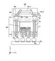
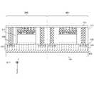
図1は、本技術の第1の実施の形態における半導体装置500の断面図の一例である。この半導体装置500は、パッケージ200、300およびパッケージ基板400を含む。<1. First Embodiment>
[Semiconductor device configuration example]
FIG. 1 is an example of a cross-sectional view of the
以下、パッケージ200および300の積層方向に平行な軸をZ軸とする。Z軸に垂直な所定の軸をX軸とし、X軸およびZ軸に垂直な軸をY軸とする。同図は、Y軸方向から見た断面図である。 Hereinafter, the axis parallel to the stacking direction of the
パッケージ200は、基板302と、その基板302に結合された積層ダイ308-1および308-2を含む。なお、積層ダイの個数は2つに限定されず、1つなどであってもよい。また、基板302は、アクティブデバイスおよびパッシブデバイス(不図示)を含んでもよい。
また、基板302は、貫通ビア306を含み、さらに配線層(不図示)を含んでもよい。配線層は、アクティブデバイスおよびパッシブデバイスの上に形成されてもよく、各種デバイスを接続して機能回路を形成するように設計されている。配線層は、誘電体(例えば、低誘電体材料)と導電性材料(例えば、銅)の層を相互に接続するビアを有する交互の層で形成されていてもよく、任意の適切なプロセス(蒸着、ダマシン、デュアルダマシンなど)によって形成される。 Further, the
基板302の両面の一方にボンドパッド303が形成され、他方にボンドパッド304が形成される。ボンドパッド303は、積層ダイ308-1や308-2に結合するために用いられる。ボンドパッド304は、パッケージ200と結合するために用いられる。
ボンドパッド303および304は、銅、チタン、ニッケル、金、パラジウム、またはそれらの組み合わせからなる薄いシード層(不図示)の上に導電性材料を堆積させて形成してもよい。導電性材料は、電気化学めっき法、無電解めっき法、CVD(Chemical Vapor Deposition)法、ALD(Atomic Layer Deposition)法、PVD(Physical Vapor Deposition)法等、またはこれらの組み合わせにより形成してもよい。ボンドパッド303および304の導電性材料として、銅、タングステン、アルミニウム、銀、金、またはそれらの組み合わせが例示される。
パッケージ基板400は、シリコンなどの半導体材料で構成される。パッケージ基板400は、アクティブデバイスおよびパッシブデバイス(不図示)を含んでもよい。パッケージ基板400はまた、配線層およびビア(不図示)と、ボンドパッド402とを含んでもよい。 The
導電性コネクタ143は、パッケージ200をボンドパッド402に取り付けるためにリフローされる。 The
パッケージ200とパッケージ基板400との間に、導電性コネクタ143を取り囲むアンダーフィル(不図示)が形成されてもよい。アンダーフィルは、パッケージ200が装着された後に毛細管流プロセスによって形成されてもよいし、パッケージ200が装着される前に適当な蒸着法によって形成されてもよい。 An underfill (not shown) surrounding the
パッケージ200は、前面再配線層120、集積回路ダイ111、貫通ビア106、封止材119、誘電体層103、誘電体層105および導電性コネクタ314を含む。
前面再配線層120の両面の一方は、導電性コネクタ143に接続され、他方には矩形の半導体チップである集積回路ダイ111が積層される。なお、前面再配線層120は、特許請求の範囲に記載の配線層の一例であり、集積回路ダイ111は、特許請求の範囲に記載の半導体チップの一例である。 One of both sides of the
また、前面再配線層120の両面のうち、集積回路ダイ111が積層された面は、封止材119を貫通する貫通ビア106を介して誘電体層105と接続される。 Further, of both surfaces of the
誘電体層105には、誘電体層103が積層される。この誘電体層103の開口部には、導電性コネクタ314が形成される。この導電性コネクタ314は、パッケージ300と接続される。 The
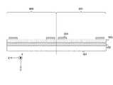
図2は、本技術の第1の実施の形態における前面再配線層120および集積回路ダイ111の断面図の一例である。同図において、前面再配線層120の一部の領域に集積回路ダイ111が積層され、残りの領域には、封止材119や貫通ビア(不図示)が設けられる。また、同図において、前面再配線層120は、図1で例示した構成よりも簡略化して記載されている。 FIG. 2 is an example of a cross-sectional view of the
また、再配線層120においては、同図におけるX-Y平面上に配線パターン126などにり信号線が配線される。この平面(配線面)上の一部の領域に集積回路ダイ111が積層され、残りの領域には、封止材119が形成される。再配線層120のX-Y平面のうち、集積回路ダイ111が積層される領域の境界線は、同図においては、座標(X2、Z0)の点を含み、Y軸に沿って伸びる直線に該当する。そして、再配線層120において、その境界線を跨いで配線パターン126により信号線が配線されるものとする。 Further, in the
ここで、集積回路ダイ111を積層した領域の境界線の近傍には、応力が集中することがある。例えば、製造工程中の熱処理などの際に、各部材のCTE(Coefficient of Thermal Expansion)の相違などに起因して、Z方向に沿って境界線の近傍に剪断応力が生じることがある。例えば、座標X1から座標X3までの領域に、応力が集中する。 Here, stress may be concentrated in the vicinity of the boundary line of the region where the integrated circuit dies 111 are stacked. For example, during heat treatment during a manufacturing process, shear stress may occur in the vicinity of the boundary line along the Z direction due to a difference in CTE (Coefficient of Thermal Expansion) of each member. For example, stress is concentrated in the region from the coordinate X1 to the coordinate X3.
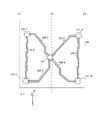
図3は、本技術の第1の実施の形態における配線パターンの一例を示す平面図である。同図は、前面再配線層120の座標X1からX3までの領域をZ軸方向から見た平面図である。前面再配線層120は、積層された2層以上の誘電体層を含むが、同図では、それらのうち1層のみを例示している。座標X1と座標X2と間に導電性ビア131-1および131-3が形成され、座標X2と座標X3との間に導電性ビア131-2および131-4が形成される。また、配線パターン126により、信号線126-1および126-2が形成される。 FIG. 3 is a plan view showing an example of a wiring pattern according to the first embodiment of the present technique. The figure is a plan view of the region from the coordinates X1 to X3 of the
信号線126-1は、集積回路ダイ111が積層される領域の境界線を跨いで、導電性ビア131-1と、導電性ビア131-2とを接続する。信号線126-2は、境界線を跨いで、導電性ビア131-3と、導電性ビア131-4とを接続する。 The signal line 126-1 straddles the boundary line of the region where the integrated circuit dies 111 are stacked, and connects the conductive via 131-1 and the conductive via 131-2. The signal line 126-2 straddles the boundary line and connects the conductive via 131-3 and the conductive via 131-4.
信号線126-1の配線パスは、複数(例えば、3つ)の線分に分割することができる。配線パスを分割した際の線分のそれぞれを以下、セグメントと称する。これらのセグメントは、境界線と交差する特定のセグメントを含み、そのセグメントと境界線とのなす角度θ1は、所定角度(例えば、50度)未満である。また、信号線126-2の配線パスは、境界線上において、その境界線に対する角度が所定角度(例えば、50度)未満の方向に屈曲する屈曲点を含む。同図における黒丸は、屈曲点を示す。この屈曲点を起点として右側に伸びるセグメントは、その一端が境界線上の所定の点(配線パスと境界線との交差点)と略一致し、境界線に対する角度が所定角度(例えば、50度)未満のセグメントである。なお、屈曲点から左側に伸びるセグメントと境界線との角度は、所定角度未満でなくともよい。すなわち、境界線で配線パスが屈曲する際は、境界線により分断される2つの領域の一方(左側)へ伸びるセグメントと、それらの領域の他方(右側)へ伸びるセグメントとの少なくとも一方の境界線に対する角度が所定角度未満であればよい。このように、前面再配線層120の配線面には、半導体ダイ111の積層される領域のいずれかの境界線により分断される2つの領域の少なくとも一方において境界線を跨ぐ際に成す角度が所定角度未満の信号線126-1や126-2が配線される。The wiring path of the signal line 126-1 can be divided into a plurality of (for example, three) line segments. Each of the line segments when the wiring path is divided is hereinafter referred to as a segment. These segments include a specific segment that intersects the boundary line, and the angle θ1 between the segment and the boundary line is less than a predetermined angle (for example, 50 degrees). Further, the wiring path of the signal line 126-2 includes a bending point on the boundary line that bends in a direction in which the angle with respect to the boundary line is less than a predetermined angle (for example, 50 degrees). Black circles in the figure indicate bending points. A segment extending to the right from this bending point has one end substantially coincided with a predetermined point on the boundary line (intersection between the wiring path and the boundary line), and the angle with respect to the boundary line is less than a predetermined angle (for example, 50 degrees). It is a segment of. The angle between the segment extending to the left from the bending point and the boundary line does not have to be less than a predetermined angle. That is, when the wiring path bends at the boundary line, at least one boundary line between a segment extending to one (left side) of two regions divided by the boundary line and a segment extending to the other (right side) of those regions. It suffices if the angle with respect to is less than a predetermined angle. As described above, the wiring surface of the
これらの場合においても、直線形状の配線パスを境界線に対して垂直に形成した場合に比べ、断線率を下げる効果があることが見出された。境界線での応力は主には境界面に垂直方向に発生するところ、信号線126-1の例では配線パスの境界線に沿った断面長さが約21/2倍以上となっていることが原因であると考えられる。信号線126-2の例では屈曲点における配線パスの強度は、直線状の配線パスのそれに比して強いことが原因であると考えられる。なお、本実施形態では境界線に対する角度を50度未満としたが、応力耐性のみを鑑みると角度は、0度に近い方が好ましいといえる。ただし、配線効率との兼ね合いから、30度乃至50度とするのが好ましい。Even in these cases, it was found that there is an effect of lowering the disconnection rate as compared with the case where the linear wiring path is formed perpendicular to the boundary line. The stress at the boundary line is mainly generated in the direction perpendicular to the boundary surface, but in the example of the signal line 126-1, the cross-sectional length along the boundary line of the wiring path is about 21/2 times or more. It is thought that this is the cause. In the example of the signal line 126-2, it is considered that the strength of the wiring path at the bending point is stronger than that of the linear wiring path. In the present embodiment, the angle with respect to the boundary line is set to less than 50 degrees, but it can be said that the angle is preferably close to 0 degrees in consideration of stress tolerance alone. However, in consideration of wiring efficiency, it is preferably 30 to 50 degrees.
[半導体装置の製造方法]
次に、図4乃至図17を参照して、半導体装置500の製造方法について説明する。[Manufacturing method of semiconductor devices]
Next, a method of manufacturing the
図4は、本技術の第1の実施の形態におけるキャリア基板101と、キャリア基板101上に形成された剥離層102とを示す図である。パッケージ200を形成するためのパッケージ領域600および601がそれぞれ図示されている。 FIG. 4 is a diagram showing a
キャリア基板101は、ガラス製やセラミック製でもよく、キャリア基板101上に複数のパッケージを同時に形成できるようなウェハであってもよい。このキャリア基板101上に剥離層102が形成される。この剥離層102は、キャリア基板101とともに、後続のステップで形成される構造体から除去されてもよい。剥離層102の材料の一例は、加熱されると接着性を失うエポキシベースの熱離型材料であり、例えば、光対熱変換型コーティング(LTHC:Light-To-Heat-Conversion Release Coating)である。他の例は、紫外線に曝されると接着性を失う紫外線(UV:UltraViolet)接着剤である。剥離層102は、液体として吐出されて硬化したものであってもよいし、キャリア基板101に積層されたラミネートフィルムであってもよい。剥離層102の上面は、平坦化されていてもよい。 The
次に、図5に例示するように、誘電体層103と配線パターン104とが形成される。誘電体層103は、剥離層102上に形成される。誘電体層103の材料の一例は、ポリベンゾオキサゾール(PBO:Poly-BenzoOxazole)、ポリイミド、ベンゾシクロブテン(BCB:BenzoCycloButene)などのポリマーである。他の例は、窒化ケイ素などの窒化物が挙げられる。このほか、酸化ケイ素、リン酸塩ガラス(PSG:Phosphrous Silicate Glass)、ホウケイ酸塩ガラス(BSG:BoroSilicate Glass)、ホウ素ドープリン酸塩ガラス(BPSG:Boro-Phospho Silicate Glass)などの酸化物が挙げられる。誘電体層103は、スピンコーティング、化学気相成長(CVD:Chemical Vapor Deposition)、ラミネートなどの任意の許容可能な堆積プロセス、またはそれらの組み合わせによって形成される。 Next, as illustrated in FIG. 5, the
誘電体層103上には、配線パターン104が形成されている。配線パターン104を形成方法の一例として、誘電体層103の上にシード層(不示)を形成する方法が挙げられる。シード層は金属層であり、これは単層または異なる材料で形成された複数の層からなっていてもよい。シード層の一例は、チタン層と、チタン層の上にある銅層とからなる。シード層は、例えば、PVD等を用いて形成してもよい。配線パターンを形成する上でのシード層の最適な膜厚は50ナノメートル(nm)から200ナノメートル(nm)である。 A
その後、フォトレジストを形成し、シード層上にパターニングする。フォトレジストは、スピンコート等で形成する。フォトレジストのパターンは、配線パターン104に対応して形成される。パターニングにより、シード層を露出させるために、フォトレジストに開口部を形成する。フォトレジストの開口部およびシード層の露出部には、導電性材料が形成される。導電性材料は、電解メッキや無電解メッキなどのメッキによって形成される。導電性材料は、銅、チタン、タングステン、アルミニウムなどの金属で構成されていてもよい。その後、フォトレジストを、酸素プラズマ等を使用したアッシング処理によって除去する。その後、シード層の露出部分は、例えば、ウェットエッチングまたはドライエッチングなどのエッチングプロセスを使用することによって除去される。シード層と導電性材料の残りの部分が配線パターン104を形成する。 Then, a photoresist is formed and patterned on the seed layer. The photoresist is formed by spin coating or the like. The photoresist pattern is formed corresponding to the
ここで後述するように、導電性材料は、シード層に接触してなる第1の部分と、シード層とは非接触となっている第2の部分とを有していてもよい。これによれば、導電性材料の第2の部分の直下にはシード層が形成されていないので、外部からの応力に追従して配線パターン104が変形し又は動くことが可能になり、応力を効果的に緩和することができる。また、配線パターン104上に後述する貫通ビアや導電性ピラーや半田ボールなどの外部端子やビアが形成された場合には、これら外部端子やビアの根元部に加えられる応力を低減することができる。 As will be described later, the conductive material may have a first portion that is in contact with the seed layer and a second portion that is not in contact with the seed layer. According to this, since the seed layer is not formed directly under the second portion of the conductive material, the
図6では、配線パターン104と誘電体層103の上に誘電体層105が形成されている。誘電体層105は、誘電体層103と同様の材料で形成され、リソグラフィマスクを用いてパターニングされる。その後、誘電体層105は、配線パターン104の一部を露出させるための開口部を形成するようにパターニングされる。パターニングは、誘電体層が感光材料である場合には、誘電体層105を光に曝すことによって、または、例えば、異方性エッチングを用いたエッチングなどのプロセスによって行われる。 In FIG. 6, the
なお、誘電体層103、105および配線パターン104は、裏面再配線層107と呼んでもよい。図示されているように、裏面再配線層107は、2つの誘電体層103、105と1つの配線パターン104とを含む。裏面再配線層107は、任意の数の誘電体層、配線パターン、およびビアを含むことができる。配線パターン104および誘電体層105を形成する工程を繰り返すことにより、1つ以上の追加の配線パターン及び誘電体層を裏面再配線層107に形成することができる。ビアは、下地誘電体層の開口部に配線パターンのシード層と導電性材料を形成することにより、配線パターンの形成中に形成される。ビアは、上下に隣接する配線パターンを相互に接続するものである。 The
さらに図6では、貫通ビア106が形成されている。貫通ビア106を形成するための例として、図示されているように、裏面再配線層107の、例えば誘電体層105および配線パターン104の露出部分の上に上述の材料、プロセスを用いてシード層(不図示)が形成される。その後、上述の材料、プロセスを用いてフォトレジストを形成し、シード層上にパターニングする。フォトレジストのパターンはスルービアに対応して形成される。フォトレジストの開口部およびシード層の露出部には、上述の材料やプロセスを用いて導電性材料が形成される。その後、フォトレジストと、導電性材料が形成されていないシード層の一部を除去する。シード層は導電性材料をマスクとしたウェットエッチングで除去しても良い。また、上述のように、導電性材料は、シード層に接触してなる第1の部分と、下地層とは非接触となっている第2の部分とを有していてもよい。残ったシード層および導電性材料が、貫通ビア106や配線パターン(不図示)となる。 Further, in FIG. 6, a penetrating via 106 is formed. As an example for forming the through via 106, as shown, a seed layer of the back
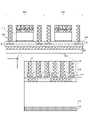
図7において、集積回路ダイ111は、接着剤112によって誘電体層105に接着されている。同図に示すように、集積回路ダイ111は、パッケージ領域600および601のそれぞれに固着されており、他の実施形態では、より多くの集積回路ダイ111が各領域に固着されていてもよい。 In FIG. 7, the integrated circuit die 111 is adhered to the
集積回路ダイ111は、ロジックダイ、メモリダイ、パワーマネージメント集積回路ダイ、RF(Radio Frequency)ダイ、センサダイ、MEMS(Micro Electro Mechanical Systems)ダイ、信号処理ダイ、フロントエンドダイなど、または、それらの組み合わせである。ロジックダイとして、例えば、中央処理装置がマイクロコントローラが用いられる。メモリダイとして、DRAM(Dynamic Random Access Memory)ダイ、SRAM(Static RAM)ダイなどが用いられる。信号処理ダイとして、デジタル信号処理(DSP:Digital Signal Processing)ダイなどが用いられる。フロントエンドダイとして、例えば、アナログフロントエンド(AFE:Analog Front End)ダイが用いられる。 The integrated circuit die 111 can be a logic die, a memory die, a power management integrated circuit die, an RF (Radio Frequency) die, a sensor die, a MEMS (Micro Electro Mechanical Systems) die, a signal processing die, a front-end die, or a combination thereof. be. As the logic die, for example, a microcontroller is used as a central processing unit. As the memory die, a DRAM (Dynamic Random Access Memory) die, a SRAM (Static RAM) die, or the like is used. As the signal processing die, a digital signal processing (DSP) die or the like is used. As the front end die, for example, an analog front end (AFE) die is used.
また、複数の集積回路ダイやダミーダイを固着する場合、異なるサイズ(例えば、異なる高さ、および/または、表面積)であってもよく、他の実施形態では、集積回路ダイ111は、同じサイズ(例えば、同じ高さ、および/または、表面積)であってもよい。 Also, when a plurality of integrated circuit dies or dummy dies are fixed, they may have different sizes (eg, different heights and / or surface areas), and in other embodiments, the integrated circuit dies 111 have the same size (eg, different heights and / or surface areas). For example, they may have the same height and / or surface area).
また、反り防止や応力緩和を目的としたダミーダイを固着してもよい。複数の集積回路ダイやダミーダイを固着する場合、各ダイの高さは異なっていても良い。特にダミーダイを固着させる場合は、後述する前面再配線層等の配線への応力の影響を少なくするため、集積回路ダイ111よりも厚さを薄くすると良い。 Further, a dummy die for the purpose of warping prevention and stress relaxation may be fixed. When a plurality of integrated circuit dies or dummy dies are fixed, the height of each die may be different. In particular, when the dummy die is fixed, the thickness may be thinner than that of the integrated circuit die 111 in order to reduce the influence of stress on the wiring such as the front rewiring layer described later.
誘電体層105に固着される前に、集積回路ダイ111は、集積回路ダイ111内に集積回路を形成するために、適用可能な製造プロセスに従って処理されている。例えば、集積回路ダイ111は、それぞれ、シリコンからなる半導体基板113を含む。なお、半導体基板113は、ゲルマニウムなどの他の半導体材料、化合物半導体、合金半導体、または、それらの組合せを含んでもよい。化合物半導体は、例えば、炭化ケイ素、ヒ素ガリウム、リン化ガリウム、リン化インジウム、ヒ素化インジウム、および/または、アンチモン化インジウムを含む。合金半導体は、シリコンゲルマニウム(SiGe)、ガリウムヒ素リン(GaAsP)、ひ化インジウムアルミニウム(AlInAs)、アルミニウムガリウム砒素(AlGaAs)などを含む。このほか、合金半導体は、ひ化ガリウムランタン(GaLnAs)、隣化ガリウムインジウム(GaInP)、ひ化りん化インジウムガリウム(GaInAsP)等を含んでもよい。トランジスタ、ダイオード、キャパシタ、抵抗器などのデバイスは、半導体基板113内または半導体基板113上に形成されてもよく、例えば、半導体基板113上の1つ以上の誘電体層の配線パターンによって形成された相互接続構造114によって相互接続されて集積回路を形成してもよい。 Prior to being fixed to the
集積回路ダイ111には、さらに、外部接続が行われるアルミニウムパッドなどのパッド115が構成される。パッド115は、集積回路ダイ111において回路が形成されるアクティブ面にある。パッシベーション膜116は、集積回路ダイ111上およびパッド115の一部に形成されている。パッシベーション膜116からパッド115に開口部が貫通している。導電性ピラー(例えば、銅などの金属からなる)などのダイコネクタ117は、パッシベーション膜116を介して開口部内にあり、それぞれのパッド115に機械的および電気的に結合されている。ダイコネクタ117は、例えば、メッキ等により形成してもよい。ダイコネクタ117は、集積回路ダイ111のそれぞれの集積回路を電気的に結合する。 The integrated circuit die 111 is further configured with a
なお、集積回路ダイ111においては、パッド115およびパッシベーション膜116の上部に、単層または複数層の再配線層を形成しても良い。形成プロセスは上述の裏面再配線層と同様である。その場合は、ダイコネクタ117は再配線層の最上層の配線に接続される。このような再配線層を形成することで、集積回路ダイ111の配線ピッチと、ダイコネクタ117の配線ピッチのギャップを緩和することができる。 In the integrated circuit die 111, a single layer or a plurality of rewiring layers may be formed on the
また、その際、配線パターンを構成する導電性材料は、シード層に接触してなる第1の部分と、シード層とは非接触となっている第2の部分とを有していてもよい。これによれば、導電性材料の第2の部分の直下にはシード層が形成されていないので、外部からの応力に追従して配線パターンが変形し又は動くことが可能になり、応力を効果的に緩和することができる。また、本実施形態にて後述するダイコネクタやビア等の端子が配線パターン上に形成される場合には、これら端子の根元部に加えられる応力を低減することができる。なお、第1の部分と第2の部分のギャップ幅Aは例えば50ナノメートル(nm)以上1000ナノメートル(nm)以下とすることが好ましい。 Further, at that time, the conductive material constituting the wiring pattern may have a first portion that is in contact with the seed layer and a second portion that is not in contact with the seed layer. .. According to this, since the seed layer is not formed directly under the second portion of the conductive material, the wiring pattern can be deformed or moved in accordance with the stress from the outside, and the stress is effective. Can be alleviated. Further, when terminals such as die connectors and vias, which will be described later in the present embodiment, are formed on the wiring pattern, the stress applied to the roots of these terminals can be reduced. The gap width A between the first portion and the second portion is preferably, for example, 50 nanometers (nm) or more and 1000 nanometers (nm) or less.
図7に戻り、誘電体材料118は、集積回路ダイ111のアクティブ面側に形成される。また、誘電体材料118は、ダイコネクタ117を封止するように形成される。誘電体材料118は、PBO、ポリイミド、BCBなどのポリマーや、窒化シリコンなどの窒化物、酸化シリコン、PSG、BSG、BPSG、BPSGなどの酸化物、またはそれらの組み合わせであってもよい。例えば、誘電体層118は、スピンコート、ラミネート、CVDなどによって形成されてもよい。 Returning to FIG. 7, the
接着剤112は、集積回路ダイ111の裏面にあり、集積回路ダイ111を図示の誘電体層105等からなる裏面再配線層107に接着する。接着剤112は、好適な接着剤、エポキシ樹脂、ダイアタッチフィルム(DAF:Die Attach Film)等の任意のものを用いることができる。接着剤112は、集積回路ダイ111の裏面、例えば各半導体ウエハの裏面に塗布されてもよいし、キャリア基板101の表面上に塗布されてもよい。集積回路ダイ111は、例えばソーイングやダイシングなどの方法で個片化され、例えばピックアンドプレースツールを用いて接着剤112によって誘電体層105に接着される。 The adhesive 112 is located on the back surface of the integrated circuit die 111, and adheres the integrated circuit die 111 to the back
図8において、封止材119はモールド用化合物(例えばエポキシ樹脂)であり、圧縮成形、転写成形等の方法で塗布される。熱や光による硬化後、封止材119は、貫通ビア106およびダイコネクタ117を露出させるために研削される。貫通ビア106、ダイコネクタ117、および封止材119の上面は、研削加工後は平坦化された形状となる。 In FIG. 8, the sealing
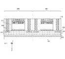
続いて、図9乃至図12を参照して、前面再配線層120の形成プロセスについて説明する。図12に図示されるように、前面再配線層120は、誘電体層121、122、123、124と、配線パターン125、126、127とを含む。 Subsequently, the process of forming the
図9において、誘電体層121は、封止材119、貫通ビア106、およびダイコネクタ117上に堆積される。例えば誘電体層121は、PBO、ポリイミド、BCBなどの感光性材料からなるポリマーで形成され、リソグラフィマスクを用いてパターニングされる。なお、誘電体層121は、窒化シリコンなどの窒化物、酸化シリコン、PSG、BSG、BPSG、BPSGなどの酸化物、などで形成されてもよい。誘電体層121は、スピンコート、ラミネート、CVD、等、またはそれらの組み合わせによって形成されてもよい。 In FIG. 9, the
図10に示されるように、その後、誘電体層121がパターニングされ、貫通ビア106およびダイコネクタ117の一部を露出させるための開口部を形成する。パターニングは、誘電体層121が感光材料である場合には、誘電体層121を露光することによってなされる。あるいは、例えば、異方性エッチングを用いたエッチングによってなど、許容されるプロセスによって行われてもよい。 As shown in FIG. 10, the
図11では、誘電体層121上にビアを有する配線パターン125が形成されている。配線パターン125を形成する例として、シード層(図示せず)が、誘電体層121の上および誘電体層121の開口部に形成される。シード層は金属層であり、これは単層または異なる材料で形成された複数の層からなっていてもよい。シード層の一例は、チタン層と、チタン層の上にある銅層とからなる。シード層は、例えば、PVD等を用いて形成してもよい。配線パターンを形成する上でのシード層の最適な膜厚は50ナノメートル(nm)から200ナノメートル(nm)である。 In FIG. 11, a
その後、フォトレジストを形成し、シード層上にパターニングする。フォトレジストは、スピンコート等で形成する。フォトレジストのパターンは、配線パターン125に対応して形成される。パターニングにより、シード層を露出させるために、フォトレジストに開口部を形成する。フォトレジストの開口部およびシード層の露出部には、導電性材料が形成される。導電性材料は、電解メッキや無電解メッキなどのメッキによって形成される。導電性材料は、銅、チタン、タングステン、アルミニウムなどの金属で構成されていてもよい。その後、フォトレジストを、酸素プラズマ等を使用したアッシング処理によって除去する。その後、シード層の露出部分は、例えば、ウェットエッチングまたはドライエッチングなどのエッチングプロセスを使用することによって除去される。シード層と導電性材料の残りの部分が配線パターン125およびビアを形成する。ビアは、誘電体層121を介して、例えば、貫通ビア106および/またはダイコネクタ117への開口部に形成される。 Then, a photoresist is formed and patterned on the seed layer. The photoresist is formed by spin coating or the like. The photoresist pattern is formed corresponding to the
以下同様のプロセスを繰り返すことにより、図12に示されるように前面再配線層120内に、誘電体層121、122、123、124と、配線パターン125、126、127とが形成される。 By repeating the same process thereafter, the
誘電体層121、122、123および124の膜厚の一例は1マイクロメートル(um)~10マイクロメートル(um)であるが、低背化の観点から5マイクロメートル(um)以下が望ましい。配線パターン125、126および127の膜厚の一例は0.5マイクロメートル(um)乃至4マイクロメートル(um)であるが、同じく低背化の観点から2um以下が望ましい。 An example of the thickness of the
前面再配線層120の下層の配線パターン(例えば、配線パターン125)についてはパターン形成し、誘電体層122で被膜後、例えばCMP(Chemical Mechanical Polishing)等による平坦化処理を行うこともできる。この場合、誘電体層122は、配線パターン125の上面を境に、平坦化処理前に形成される下部層と、平坦化処理後に形成される上部層に分かれて形成される。このようにすることによりチップ全体の平坦化度が向上する。また、配線パターン125を、126と127に比べて厚く形成してもよい。例えば、配線パターン125を3マイクロメートル(um)、配線パターン126および127を2マイクロメートル(um)にしてもよい。これにより、例えば配線パターン125のビアの上面に凹部が形成されることなく、より平坦化度が向上する。 The wiring pattern (for example, wiring pattern 125) of the lower layer of the
また、配線パターン125、126および127の配線ピッチの一例は1マイクロメートル(um)乃至10マイクロメートル(um)であるが、微細化の観点から5マイクロメートル(um)以下が望ましい。 Further, an example of the wiring pitch of the
次に、図13?図17は、図12の後のさらなるプロセス中の中間ステップの断面図を示す。 Next, FIGS. 13-17 show cross-sectional views of intermediate steps during the further process after FIG.
図13では、その後、誘電体層124がパターニングされる。パターニングは、上述のプロセスにより実施される。ここで、前面再配線層120には、更に多くまたはより少ない誘電体層および配線パターンが形成されていてもよい。 In FIG. 13, the
図14において、アンダーバンプメタル(UBM:Under Barrier Metal)142は、前面再配線層120の外側面に形成される。アンダーバンプメタル142は、導電性コネクタ143に結合するために使用される。図示された実施形態では、アンダーバンプメタル142は、誘電体層124に形成された開口部を介して配線パターン127に接続される。 In FIG. 14, the under bump metal (UBM) 142 is formed on the outer surface of the
図15では、導電性コネクタ143がアンダーバンプメタル142上に形成される。導電性コネクタ143は、BGA(Ball Grid Array)コネクタ、半田ボール、金属柱、C4バンプ、マイクロバンプ、ENEPIG(Electroless Nickel Electroless Palladium Immersion Gold)法で形成されたバンプなどであってもよい。導電性コネクタ143は、はんだ、銅、アルミニウム、金、ニッケル、銀、パラジウム、スズ、またはそれらの組み合わせなどの導電性材料を含んでもよい。導電性コネクタ143は、蒸発、電気メッキ、印刷、半田転写、ボール配置などのような一般的に使用される方法によって、最初に半田の層を形成することによって形成される。はんだの層が形成された後、はんだの層を所望のバンプ形状に成形するためにリフローを行ってもよい。 In FIG. 15, the
図16において、キャリア基板101が裏面再配線層107の誘電体層103から剥離される。キャリア基板101の剥離は、光の熱の下で剥離層102が分解し、キャリア基板101を除去することができるように、レーザ光またはUV光などの光を剥離層102上に照射することで行うことができる。そして、この構造体を裏返してテープ144上に載せる。 In FIG. 16, the
同図にさらに図示されているように、誘電体層103に、配線パターン104の一部を露出させる開口部が形成される。開口部は、例えば、レーザー穿孔、エッチング等を用いて形成される。 As further illustrated in the figure, the
図17において、個片化工程は、スクライブライン領域に沿って、隣接するパッケージ領域600と601との間でダイシングすることによって実行される。 In FIG. 17, the individualization step is performed by dicing between
このように、本技術の第1の実施の形態によれば、境界線により分断される2つの領域の少なくとも一方において境界線を跨ぐ際に成す角度が所定角度未満の信号線を配線したため、境界線近傍の応力による断線を防止することができる。断線の防止により、半導体装置500の信頼性を向上させることができる。 As described above, according to the first embodiment of the present technique, since the signal line whose angle formed when straddling the boundary line is less than a predetermined angle is wired in at least one of the two regions divided by the boundary line, the boundary is formed. It is possible to prevent disconnection due to stress near the line. By preventing disconnection, the reliability of the
<2.第2の実施の形態>
上述の第1の実施の形態では、境界線との間の角度が所定角度未満のセグメントを含む信号線126-1などを配線していたが、誘電体層103や105において境界線近傍の外部端子に応力が集中することも考えられる。この第2の実施の形態の半導体装置500は、外部端子への応力を緩和する点において第1の実施の形態と異なる。<2. Second Embodiment>
In the above-mentioned first embodiment, the signal line 126-1 or the like including the segment whose angle with the boundary line is less than a predetermined angle is wired, but the outside of the vicinity of the boundary line in the
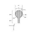
図18は、本技術の第2の実施の形態における誘電体層103および105の断面図の一例である。同図は、シード層245の不要な領域を除去し、さらに、配線パターン104と誘電体層103の上に誘電体層105が形成された後のY方向から見た断面図である。 FIG. 18 is an example of a cross-sectional view of the
誘電体層105には、外部端子246が形成される。この外部端子246の下部には、導電性材料240が形成される。導電性材料240の両面のうち一方は、外部端子246に接続される。また、導電性材料240の両面のうち他方は、シード層245に接触する第1の部分と、シード層245とは非接触の第2の部分とを有する。同図において、導電性材料240の下面のうち幅dXAの部分が、第1の部分に該当し、その両側の幅dXBの部分が、第2の部分に該当する。An
第1の部分は、シード層245にオーバーラップしており、第2の部分は、シード層245にオーバーラップしていない。このような形状はシード層245を、導電性材料240をマスクとしたエッチングプロセスにより除去する際に、導電性材料240の領域よりもオーバーエッチングすることで形成される。ウェットエッチングの場合、エッチャントが導電性材料240の領域よりも内側に進入するようにエッチング量を例えば時間でコントロールすることで形成される。 The first portion overlaps the
これによれば、導電性材料240の第2の部分の直下にはシード層245が形成されていないので、外部からの応力に追従して導電性材料240が変形し又は動くことが可能になり、応力を効果的に緩和することができる。また、導電性材料240上に貫通ビアや導電性ピラーや半田ボールなどの外部端子246(図は半田ボールの例)やビア(図示せず)が形成された場合には、これら外部端子246やビアの根元部に加えられる応力を低減することができる。 According to this, since the
第2の部分の幅dXAは、導電性材料240が膜厚が約5マイクロメートル(μm)の銅(Cu)からなる場合は、50ナノメートル(nm)以上、1000ナノメートル(nm)以下とすることが好ましい。The widthdXA of the second portion is 50 nanometers (nm) or more and 1000 nanometers (nm) or less when the
また、第1の部分の幅dXBと、導電性材料240の露出部(すなわち、誘電体層105の開口部)の幅dXCとは、次の式に示す関係を有してもよい。
dXB<dXC ・・・式1Further, the widthdXB of the first portion and the widthdXC of the exposed portion (that is, the opening of the dielectric layer 105) of the
dXB <dXC ...
こうすることで、導電性材料240と、外部端子246またはビアの接触部分の内側にシード層245が配置される。この結果、導電性材料240の露出部に加えられる応力(外部端子246またはビアの根元部に加えられる応力)に対する、導電性材料240と、外部端子246またはビアの自由度がより向上し、応力を効果的に緩和することができる。 By doing so, the
また、同図において、導電性材料240の上面の幅と、導電性材料240の露出部(誘電体層105の開口部)の幅dXCとは0~数十ナノメートル(nm)のズレで略一致させてもよい。すなわち、半田ボール等の外部端子246やビア(不図示)等が、導電性材料240の上面の全面にわたって導電性材料240と接続されていてもよい。こうすることで第2の部分による外部端子246またはビアの自由度の向上、および応力緩和の効果を高めることができる。Further, in the figure, the width of the upper surface of the
また、同図において、第2の部分は、空乏(空気層)でも良いが、誘電体層105で埋められていてもよい。これによれば、誘電体層105がシード層245よりも柔らかい場合に、導電性材料240の自由度が向上し、応力を緩和することができる。 Further, in the figure, the second portion may be depleted (air layer), but may be filled with the
図19は、Z軸方向から見た導電性材料240の平面図である。同図に示すように、導電性材料240は線状のライン部243と、円形や楕円形のランド部244とを有する。ライン部243とランド部244の接続部を除き、第1の部分の全周に第2の部分が配置されていてもよい。その場合、第2の部分は、第1の部分の全周にほぼ一定の幅(ライン部243およびランド部244の接続部付近を除く)を有して配置されていてもよい。 FIG. 19 is a plan view of the
ランド部244がシード層245を介して誘電体層103上に形成されている場合、ランド部244の第2の部分は、誘電体層103から間隔をあけて配置されている。また、図18で述べたように、この間隔は空乏(空気層)でも良いが、誘電体層105で埋められていてもよい。このような構成をとることで、導電性材料240と、外部端子246またはビアの自由度がより向上し、応力を効果的に緩和することができる。 When the
なお、第2の実施の形態に、第1の実施の形態を適用することもできる。 The first embodiment can also be applied to the second embodiment.
このように、本技術の第2の実施の形態によれば、導電性材料240がシード層245に接触する部分と、シード層245に非接触の部分とを有するため、誘電体層103等の境界線近傍に生じる応力を緩和することができる。 As described above, according to the second embodiment of the present technique, since the
[第1の変形例]
上述の第2の実施の形態では、導電性材料240にシード層245に接触する部分とシード層245とは非接触部分とを設けていたが、この構成でも応力を緩和しきれないことがある。この第2の実施の形態の第1の変形例の半導体装置500は、導電性材料240の端面をテーパー状とする点において第2の実施の形態と異なる。[First modification]
In the second embodiment described above, the
図20は、本技術の第2の実施の形態の第1の変形例における誘電体層103および105の断面図の一例である。この第2の実施の形態の第1の変形例の導電性材料240の上面(同図では、外部端子246に接続される面)は、下面よりも面積が広い。これにより、導電性材料240の端面はテーパー状となる。 FIG. 20 is an example of a cross-sectional view of the
導電性材料240と、外部端子246またはビアの自由度に寄与するのは導電性材料240の上面の端面と下面の端面のギャップ、および導電性材料240の下面の端面からシード層245の端面までの距離(すなわち幅dXA)の総和である。このため、一方で導電性材料240に対するシード層245のカバレッジを維持しつつ、他方で特に式1の関係を満たす場合は、導電性材料240と、外部端子246またはビアの自由度を向上させることができる。これにより、応力を効果的に緩和することができる。なお導電性材料240の上面と下面の端面の水平方向の差は50ナノメートル(nm)乃至1000ナノメートル(nm)程度が望ましい。It is the gap between the upper surface end face and the lower surface end face of the
このように、本技術の第2の実施の形態の第1の変形例によれば、導電性材料240の端面をテーパー状に形成したため、応力をより効果的に緩和することができる。 As described above, according to the first modification of the second embodiment of the present technique, since the end face of the
[第2の変形例]
上述の第2の実施の形態では、導電性材料240がライン部243およびランド部244を有するが、この構成では、応力を十分に緩和することができないことがある。この第2の実施の形態の第2の変形例の半導体装置500は、複数のランド部244を設けた点において第2の実施の形態と異なる。[Second modification]
In the second embodiment described above, the
図21は、本技術の第2の実施の形態第2の変形例における誘電体層103の平面図の一例である。誘電体層103において、導電性材料240は、複数のランド部244を含む。ランド部244の間には、ライン部243が形成される。これによると、接続部における配線抵抗を半分にできる。また、どちらかに接続される端子(外部端子246やビア)で断線が生じた場合でも機能を維持することができる。また上述のように第2の部分を有することにより、導電性材料240と、外部端子246またはビアの自由度がより向上し、応力をより効果的に緩和することができる。 FIG. 21 is an example of a plan view of the
なお、第2の実施の形態の第2の変形例に、第1の実施の形態や、第2の実施の形態の第1の変形例を適用することもできる。 It should be noted that the first modification and the first modification of the second embodiment can also be applied to the second modification of the second embodiment.
このように、本技術の第2の実施の形態の第2の変形例では、導電性材料240が複数のランド部244を有するため、配線抵抗を低減し、応力をより効果的に緩和することができる。 As described above, in the second modification of the second embodiment of the present technique, since the
<3.第3の実施の形態>
上述の第1の実施の形態では、境界線との間の角度が所定角度未満の特定のセグメントを含む信号線126-1などを配線していたが、この構成では、応力を十分に緩和することができないことがある。この第3の実施の形態の半導体装置500は、境界線と交差するセグメントの幅を広くする点において、第1の実施の形態と異なる。<3. Third Embodiment>
In the above-mentioned first embodiment, the signal line 126-1 or the like including a specific segment whose angle with the boundary line is less than a predetermined angle is wired, but in this configuration, the stress is sufficiently relaxed. Sometimes you can't. The
図22は、本技術の第3の実施の形態における配線パターンの一例を示す平面図である。この第3の実施の形態においても、信号線126-1は、集積回路ダイ111が積層される領域の境界線を跨いで、導電性ビア131-1と、導電性ビア131-2とを接続する。信号線126-2は、境界線を跨いで、導電性ビア131-3と、導電性ビア131-4とを接続する。 FIG. 22 is a plan view showing an example of a wiring pattern according to a third embodiment of the present technique. Also in this third embodiment, the signal line 126-1 straddles the boundary line of the region where the integrated circuit die 111 is laminated, and connects the conductive via 131-1 and the conductive via 131-2. do. The signal line 126-2 straddles the boundary line and connects the conductive via 131-3 and the conductive via 131-4.
ただし、信号線126-1の配線パスは、境界線と交差する特定のセグメントと、交差しないセグメントとを含む。境界線と交差するセグメントの幅は、交差しないセグメントの幅よりも広い。信号線126-2についても同様である。 However, the wiring path of the signal line 126-1 includes a specific segment that intersects the boundary line and a segment that does not intersect. The width of the segment that intersects the boundary is wider than the width of the segment that does not intersect. The same applies to the signal line 126-2.
応力による断線の発生率は、同図に例示するように、セグメントの幅を変えることによって低減されることが観察された。例えば、交差するセグメントの幅を、交差しないセグメントの幅Wの2倍の2Wとした場合は、それらを同一とした場合に比べて、断線率を50%以上減少させることができることが観察された。 It was observed that the rate of disconnection due to stress was reduced by changing the width of the segment, as illustrated in the figure. For example, when the width of the intersecting segments is 2W, which is twice the width W of the non-intersecting segments, it is observed that the disconnection rate can be reduced by 50% or more as compared with the case where they are the same. ..
また、図23に例示するように、第1の実施の形態と同様に、境界線に対して所定角度未満のセグメントの幅を広くすることもできる。 Further, as illustrated in FIG. 23, the width of the segment less than a predetermined angle with respect to the boundary line can be widened as in the first embodiment.
上述のとおり配線パスの幅方向の寸法を大きくすることは断線防止の観点で有利であるが、配線密度の観点からすると、配線パスの幅方向の寸法は小さい方が望ましい。したがって、幅が2W(例えば、10μm)のセグメントの長さはなるべく短い方が望ましい。例えば、半導体基板113の上面から配線パスまでの距離をLとした場合に、境界線を中心に少なくとも配線パスのセグメントを5×L(今回の実験例の場合の実測値は100μm)延在させた際、応力による配線パスの断線の発生を抑えることができた。 As described above, increasing the width direction dimension of the wiring path is advantageous from the viewpoint of preventing disconnection, but from the viewpoint of wiring density, it is desirable that the width direction dimension of the wiring path is small. Therefore, it is desirable that the length of the segment having a width of 2 W (for example, 10 μm) is as short as possible. For example, when the distance from the upper surface of the
また、第3の実施の形態に、第2の実施の形態や、その第1および第2の変形例を適用することもできる。 Further, the second embodiment and the first and second variants thereof can also be applied to the third embodiment.
このように、本技術の第3の実施の形態によれば、境界線と交差するセグメントの幅を、交際しないセグメントよりも広くしたため、境界線の近傍に生じる応力を緩和することができる。 As described above, according to the third embodiment of the present technique, the width of the segment intersecting the boundary line is made wider than that of the non-intersecting segment, so that the stress generated in the vicinity of the boundary line can be relaxed.
<4.第4の実施の形態>
上述の第1の実施の形態では、配線パス内の1つのセグメントについて境界線との角度を所定角度未満としていたが、この構成では、応力を十分に緩和することができないことがある。この第4の実施の形態の半導体装置500は、境界線から所定距離内のセグメントの全てについて、境界線との角度を所定角度未満とした点において第1の実施の形態と異なる。<4. Fourth Embodiment>
In the first embodiment described above, the angle with the boundary line of one segment in the wiring path is set to be less than a predetermined angle, but in this configuration, the stress may not be sufficiently relieved. The
図24は、本技術の第4の実施の形態における配線パターンの一例を示す平面図である。この第4の実施形態では信号線126-1および126-2のそれぞれの配線パスが、5つのセグメントに分けられている。この実施形態では、集積回路ダイ111の下面から配線パスまでの距離をLとする。そして、前面再配線層120において、境界線を中心として境界線と直交する方向に少なくとも5×L(今回の例では100um)の領域においては、配線パスの全てのセグメントにおいて、境界線に対する角度が50度以下となるように配置されている。言い換えれば、境界線からの距離が所定距離(5×Lなど)以内の領域内のセグメントの全てについて、境界線とのなす角度が所定角度未満である。上述のとおり、境界線での応力は主には境界面に垂直方向(90度方向)に発生するため、このような構成をとることにより、境界線の近傍の全ての配線パスにおける応力耐性を向上させることができる。 FIG. 24 is a plan view showing an example of a wiring pattern according to a fourth embodiment of the present technique. In this fourth embodiment, each wiring path of the signal lines 126-1 and 126-2 is divided into five segments. In this embodiment, the distance from the lower surface of the integrated circuit die 111 to the wiring path is L. Then, in the
また、信号線126-1および126-2のそれぞれの配線パスでは2箇所について境界線に沿って(0度方向に)延在しているセグメントを有する。このようにすることで、境界線に対して0度以外の角度を持つ各セグメントの距離を短くすることでができ、断線リスクをより減らすことが可能となる。 Further, each wiring path of the signal lines 126-1 and 126-2 has segments extending along the boundary line (in the 0 degree direction) at two points. By doing so, the distance of each segment having an angle other than 0 degrees with respect to the boundary line can be shortened, and the risk of disconnection can be further reduced.
なお、同図では、信号線の幅を一定(例えば、5μm)としているが、境界線に対して0度以外の角度を持つ各セグメントの幅を、境界線に沿って(0度方向に)延在しているセグメントの幅よりも大きく(例えば、2倍の10μmに)することもできる。これにより、断線リスクをより減らすことができる。 In the figure, the width of the signal line is constant (for example, 5 μm), but the width of each segment having an angle other than 0 degrees with respect to the boundary line is set along the boundary line (in the direction of 0 degrees). It can also be larger than the width of the extending segment (eg, doubled to 10 μm). This makes it possible to further reduce the risk of disconnection.
なお、第4の実施の形態に、第1乃至第3の実施の形態や、それらの変形例を適用することもできる。 It should be noted that the first to third embodiments and variations thereof can also be applied to the fourth embodiment.
このように本技術の第4の実施の形態では、境界線から所定距離以内の領域内のセグメントの全てについて、境界線とのなす角度を所定角度未満としたため、配線パスにおける応力耐性をさらに向上させることができる。 As described above, in the fourth embodiment of the present technique, the angle formed with the boundary line is set to be less than the predetermined angle for all the segments in the region within a predetermined distance from the boundary line, so that the stress tolerance in the wiring path is further improved. Can be made to.
<5.第5の実施の形態>
上述の第1の実施の形態では、境界線との間の角度が所定角度未満のセグメントを含む信号線126-1などを配線していたが、この構成では、半導体装置500の信頼性が不足するおそれがある。この第5の実施の形態の半導体装置500は、冗長化により信頼性を向上させた点において第1の実施の形態と異なる。<5. Fifth Embodiment>
In the first embodiment described above, a signal line 126-1 or the like including a segment whose angle with the boundary line is less than a predetermined angle is wired, but in this configuration, the reliability of the
図25は、本技術の第5の実施の形態における配線パターンの一例を示す平面図である。この第5の実施形態では、導電性ビア131-1と131-3とが、集積回路ダイ111と封止材119との間の境界線を越えない信号線126-3によって互いに電気的に接続されている。また、導電性ビア131-2と導電性ビア131-4とが、境界線を越えない信号線126-4によって互いに電気的に接続されている。 FIG. 25 is a plan view showing an example of a wiring pattern according to a fifth embodiment of the present technique. In this fifth embodiment, the conductive vias 131-1 and 131-3 are electrically connected to each other by a signal line 126-3 that does not cross the boundary between the integrated circuit die 111 and the
例えば、導電性ビア131-1と導電性ビア131-2との間で信号をやり取りする必要がある場合、必要な配線パスは、信号線126-1のパスのみであり、信号線126-2乃至126-3を経由するパスは、冗長パスである。信号線126-1の配線パスと、冗長パスとの両方に配線することにより、いずれかが断線した場合であっても、電子デバイスを正常に機能させることができ、信頼性が向上する。 For example, when it is necessary to exchange a signal between the conductive via 131-1 and the conductive via 131-2, the required wiring path is only the path of the signal line 126-1 and the signal line 126-2. The path via 126-3 is a redundant path. By wiring to both the wiring path of the signal line 126-1 and the redundant path, the electronic device can function normally even if one of them is disconnected, and the reliability is improved.
また、この実施形態では、信号線126-1および126-2の配線パスにおいて、集積回路ダイ111と封止材119との間の境界線への進入角度が互いに異なる。こうすることにより、境界線に対して90度以外の角度を持った応力が発生した場合においても、2本のパス全体としての応力耐性を向上させることができる。 Further, in this embodiment, in the wiring paths of the signal lines 126-1 and 126-2, the approach angles to the boundary line between the integrated circuit die 111 and the sealing
なお、第5の実施の形態に、第1乃至第4の実施の形態や、それらの変形例を適用することもできる。 It should be noted that the first to fourth embodiments and variations thereof can also be applied to the fifth embodiment.
このように、本技術の第5の実施の形態によれば、信号線126-1の配線パスと冗長パスとの両方に信号線を配線したため、信頼性を向上させることができる。 As described above, according to the fifth embodiment of the present technique, since the signal lines are wired to both the wiring path and the redundant path of the signal line 126-1, the reliability can be improved.
[変形例]
上述の第5の実施の形態では、冗長化により信頼性を向上させていたが、この構成では、応力に対する耐性が不足するおそれがある。この第5の実施の形態の変形例の半導体装置500は、中継ビアを設けることにより、応力耐性を向上させた点において第5の実施の形態と異なる。[Modification example]
In the fifth embodiment described above, the reliability is improved by the redundancy, but in this configuration, the resistance to stress may be insufficient. The
図26は、本技術の第5の実施の形態の変形例における配線パターンの一例を示す平面図である。この第5の実施の形態の変形例の前面再配線層120には、境界線上に中継ビア141がさらに配置される。 FIG. 26 is a plan view showing an example of a wiring pattern in a modified example of the fifth embodiment of the present technique. A relay via 141 is further arranged on the boundary line in the
また、導電性ビア131-1と中継ビア141との間に信号線126-1が配線され、導電性ビア131-2と中継ビア141との間に信号線126-2が配線される。導電性ビア131-3と中継ビア141との間に信号線126-3が配線され、導電性ビア131-4と中継ビア141との間に信号線126-4が配線される。導電性ビア131-1と導電性ビア131-3との間に信号線126-5が配線され、導電性ビア131-2と導電性ビア131-4との間に信号線126-6が配線される。中継ビア141に接続される信号線のそれぞれを異なる層に形成してもよい。 Further, the signal line 126-1 is wired between the conductive via 131-1 and the relay via 141, and the signal line 126-2 is wired between the conductive via 131-2 and the relay via 141. The signal line 126-3 is wired between the conductive via 131-3 and the relay via 141, and the signal line 126-4 is wired between the conductive via 131-4 and the relay via 141. The signal line 126-5 is wired between the conductive via 131-1 and the conductive via 131-3, and the signal line 126-6 is wired between the conductive via 131-2 and the conductive via 131-4. Will be done. Each of the signal lines connected to the relay via 141 may be formed in different layers.
例えば、信号線126-1および126-2の配線パスに対し、信号線126-3乃至126-6のパスは、冗長パスである。なお、信号線126-3乃至126-6は、冗長信号線の一例である。 For example, the paths of the signal lines 126-3 to 126-6 are redundant paths with respect to the wiring paths of the signal lines 126-1 and 126-2. The signal lines 126-3 to 126-6 are examples of redundant signal lines.
境界線上への中継ビア141の配置により、応力に対する耐性を向上させることができる。また、同図に示すように信号線126-1と信号線126-2とで互いに境界線への進入角度を異ならせることで、境界線において境界線に対して90度以外の角度を持った応力が発生した場合においても、応力耐性を向上させることができる。 By arranging the relay via 141 on the boundary line, the resistance to stress can be improved. Further, as shown in the figure, by making the approach angle to the boundary line different between the signal line 126-1 and the signal line 126-2, the boundary line has an angle other than 90 degrees with respect to the boundary line. Even when stress is generated, stress tolerance can be improved.
図27は、本技術の第5の実施の形態の変形例における前面再配線層120の断面図の一例である。同図に例示するように、境界線上に中継ビア141が配置される。 FIG. 27 is an example of a cross-sectional view of the
上述のとおり図3、図22乃至図26で述べた配線パスは、前面再配線層120を構成する誘電体層121、122、123、124上に各々存在する、配線パターン125、126、127の何れかを構成する配線パスである。この配線パスに関して、境界線近傍の所定領域における配線パターンの密度、すなわち、境界線の所定領域を越えて延在する配線パスの本数を、集積回路ダイ111から遠くなるにつれて大きくすることも有効である。集積回路ダイ111からの応力は、集積回路ダイ111から遠くなるにつれて小さくなるからである。 As described above, the wiring paths described in FIGS. 3, 22 to 26 are the
例えば、前面再配線層120においては、配線パターン125が集積回路ダイ111に最も近く、配線パターン127が最も遠い。したがって例えば配線パターン127における境界線における配線パターンの密度を、配線パターン125におけるそれよりも大きくする。こうすることで、より多くの境界線を越えて延在する配線パスを集積回路ダイ111から離して構成することができる。また、配線パターン125における境界線を越えて延在する配線パスの本数は小さくなるため、各配線パスの幅を大きくとり、応力への耐性を向上させることが可能となる。 For example, in the
また、同様に、集積回路ダイからの距離が相対的に小さい配線パターン(前面再配線層120においては、例えば配線パターン125)のみ上述の図3、図22乃至図26のいずれかで示される配線パス配置を採用することもできる。その一方で、集積回路ダイからの距離が相対的に大きい配線パターン(前面再配線層120においては、例えば配線パターン126または127)においては、境界線に垂直で、かつ、各セグメントの幅が同一の配線パスを採用することもできる。これにより、配線効率を上げるという手法も、配線効率と応力耐性の両立の観点で有用である。 Similarly, only the wiring pattern in which the distance from the integrated circuit die is relatively small (for example, the
なお、第5の実施の形態の変形例に、第1乃至第4の実施の形態や、それらの変形例を適用することもできる。 It should be noted that the first to fourth embodiments and the modified examples thereof can also be applied to the modified examples of the fifth embodiment.
このように、本技術の第5の実施の形態の変形例によれば、境界線に中継ビア141を配置したため、応力耐性を向上させることができる。 As described above, according to the modification of the fifth embodiment of the present technique, since the relay via 141 is arranged at the boundary line, the stress tolerance can be improved.
<6.第6の実施の形態>
上述の第1の実施の形態では、境界線との間の角度が所定角度未満のセグメントを含む信号線126-1などを配線していたが、この構成では、電源安定性や応力耐性が不足することがある。この第6の実施の形態の半導体装置500は、電源やグランドをメッシュ状やベタ状に敷き詰めた点において第1の実施の形態と異なる。<6. 6th Embodiment>
In the first embodiment described above, a signal line 126-1 or the like including a segment whose angle between the boundary line and the boundary line is less than a predetermined angle is wired, but in this configuration, power supply stability and stress tolerance are insufficient. I have something to do. The
図28は、本技術の第6の実施の形態における前面再配線層120の平面図の一例である。同図における一点鎖線は、集積回路ダイ111が積層される領域の境界線を示す。境界線の近傍において、電源グランド領域128と、信号線領域129とが設けられる。同図において、斜線の領域は、電源グランド領域128を示す。灰色の領域は、信号線領域129を示す。電源グランド領域128および信号線領域129のそれぞれの形状は、例えば、矩形(長方形など)である。 FIG. 28 is an example of a plan view of the
電源グランド領域128は、集積回路ダイ111への電源およびグランドの少なくとも一方が供給される領域である。電源グランド領域128には、例えば、電源線およびグランド線の少なくとも一方が、メッシュ状に配線される。あるいは、電源グランド領域128には、電源やグランドがベタパターンにより形成される。このようにすることで電源安定性と応力耐性の双方を向上させることができる。信号線領域129には、図3などに例示した配線パターンにより信号線のみが配線される。 The power
図29は、本技術の第6の実施の形態における電源グランド領域128の一構成例を示す図である。同図に例示するように、電源グランド領域128には、信号線126-1などの信号線を配線することもできる。その周囲の斜線の領域は、電源やグランドのベタパターンを示す。このような構成をとることで、ベタ状ないしメッシュ状の電源配線がシールドとなり、信号配線の応力耐性を向上させることが可能となる。 FIG. 29 is a diagram showing a configuration example of the power
なお、上記では前面再配線層120を例として説明したが、裏面再配線層107においても同様の構成をとることが可能である。 Although the
また、第6の実施の形態に、第1乃至第5の実施の形態や、それらの変形例を適用することもできる。 Further, the first to fifth embodiments and variations thereof can be applied to the sixth embodiment.
このように、本技術の第6の実施の形態によれば、境界線の近傍に電源やグランドをメッシュ状またはベタ状に設けたため、電源安定性や応力耐性を向上させることができる。 As described above, according to the sixth embodiment of the present technique, since the power supply and the ground are provided in a mesh shape or a solid shape in the vicinity of the boundary line, the power supply stability and the stress resistance can be improved.
[変形例]
上述の第6の実施の形態では、矩形の電源グランド領域128および信号線領域129を配置していた。しかし、信号線が境界線に対して斜めに配線される場合は、配線パスが形成されないデッドスペースが生じ、配線効率が低下するおそれがある。この第6の実施の形態の変形例の半導体装置500は、配線効率を向上させた点において第6の実施の形態と異なる。[Modification example]
In the sixth embodiment described above, the rectangular power
図30は、本技術の第6の実施の形態の変形例における前面再配線層120の平面図の一例である。この第6の実施の形態の変形例の前面再配線層120において、電源グランド領域128および信号線領域129の境目と、集積回路ダイ111が積層される領域の境界線とのなす角度は、90度と異なる角度(例えば、45度)である。これにより、デッドスペースを削減し、配線効率を向上させることができる。 FIG. 30 is an example of a plan view of the
なお、第6の実施の形態の変形例に、第1乃至第5の実施の形態や、それらの変形例を適用することもできる。 It should be noted that the first to fifth embodiments and their modified examples can also be applied to the modified examples of the sixth embodiment.
このように、本技術の第6の実施の形態の変形例では、電源グランド領域128および信号線領域129の境目と、集積回路ダイ111が積層される領域の境界線とのなす角度が90度と異なるため、デッドスペースを削減して配線効率を向上させることができる。 As described above, in the modified example of the sixth embodiment of the present technology, the angle formed by the boundary line between the power
<7.第7の実施の形態>
上述の第1の実施の形態では、パッケージ200にパッケージ300を積層したPoP構造に、図3に例示した配線パターンを適用していた。しかし、図3の配線パターンは、WCSP(Wafer level Chip Size Package)などのPoP構造以外のパッケージに適用することもできる。この第7の実施の形態の半導体装置500は、WCSPなどを含む点において第1の実施の形態と異なる。<7. Seventh Embodiment>
In the first embodiment described above, the wiring pattern illustrated in FIG. 3 is applied to the PoP structure in which the
図31は、本技術の第7の実施の形態における半導体装置500の断面図の一例である。同図に例示するように、半導体装置500は、集積回路ダイ111に配線層150を積層したWCSPを含む。このWCSPに、図3などに例示した配線パターンを適用することができる。これにより、WCSPの信頼性を向上させることができる。 FIG. 31 is an example of a cross-sectional view of the
なお、図32に例示するように、C4バンプによるフリップチップ接続を採用したFBGAパッケージのインターポーザ基板の配線層150に図3等の配線パターンを適用することもできる。 As illustrated in FIG. 32, the wiring pattern shown in FIG. 3 can be applied to the
また、図33に例示するように、ワイヤボンディング接続を採用したFBGAパッケージのインターポーザ基板の配線層150に、図3等の配線パターンを適用することもできる。 Further, as illustrated in FIG. 33, the wiring pattern shown in FIG. 3 or the like can be applied to the
また、図34に例示したIC実装基板においても、図3等の配線パターンを適用することもできる。このIC実装基板の配線層150の内部には、集積回路ダイ111が設けられ、集積回路ダイ111と対向する領域に配置された配線パスについて図3等の配線パターンが適用される。 Further, the wiring pattern shown in FIG. 3 can also be applied to the IC mounting board illustrated in FIG. 34. An integrated circuit die 111 is provided inside the
なお、第7の実施の形態に、第1乃至第6の実施の形態や、それらの変形例を適用することもできる。 It should be noted that the first to sixth embodiments and variations thereof can also be applied to the seventh embodiment.
このように、本技術の第7の実施の形態では、WCSPなどにおいて、境界線との間の角度が所定角度未満のセグメントを含む複数のセグメントに分割され、境界線を跨ぐに信号線を配線したため、WCSP等の信頼性を向上させることができる。 As described above, in the seventh embodiment of the present technique, in WCSP or the like, the segment is divided into a plurality of segments including a segment whose angle with the boundary line is less than a predetermined angle, and a signal line is wired across the boundary line. Therefore, the reliability of WCSP and the like can be improved.
<8.移動体への応用例>
本開示に係る技術(本技術)は、様々な製品へ応用することができる。例えば、本開示に係る技術は、自動車、電気自動車、ハイブリッド電気自動車、自動二輪車、自転車、パーソナルモビリティ、飛行機、ドローン、船舶、ロボット等のいずれかの種類の移動体に搭載される装置として実現されてもよい。<8. Application example to moving body>
The technique according to the present disclosure (the present technique) can be applied to various products. For example, the technology according to the present disclosure is realized as a device mounted on a moving body of any kind such as an automobile, an electric vehicle, a hybrid electric vehicle, a motorcycle, a bicycle, a personal mobility, an airplane, a drone, a ship, and a robot. You may.
図35は、本開示に係る技術が適用され得る移動体制御システムの一例である車両制御システムの概略的な構成例を示すブロック図である。 FIG. 35 is a block diagram showing a schematic configuration example of a vehicle control system, which is an example of a moving body control system to which the technique according to the present disclosure can be applied.
車両制御システム12000は、通信ネットワーク12001を介して接続された複数の電子制御ユニットを備える。図35に示した例では、車両制御システム12000は、駆動系制御ユニット12010、ボディ系制御ユニット12020、車外情報検出ユニット12030、車内情報検出ユニット12040、及び統合制御ユニット12050を備える。また、統合制御ユニット12050の機能構成として、マイクロコンピュータ12051、音声画像出力部12052、及び車載ネットワークI/F(interface)12053が図示されている。 The
駆動系制御ユニット12010は、各種プログラムにしたがって車両の駆動系に関連する装置の動作を制御する。例えば、駆動系制御ユニット12010は、内燃機関又は駆動用モータ等の車両の駆動力を発生させるための駆動力発生装置、駆動力を車輪に伝達するための駆動力伝達機構、車両の舵角を調節するステアリング機構、及び、車両の制動力を発生させる制動装置等の制御装置として機能する。 The drive
ボディ系制御ユニット12020は、各種プログラムにしたがって車体に装備された各種装置の動作を制御する。例えば、ボディ系制御ユニット12020は、キーレスエントリシステム、スマートキーシステム、パワーウィンドウ装置、あるいは、ヘッドランプ、バックランプ、ブレーキランプ、ウィンカー又はフォグランプ等の各種ランプの制御装置として機能する。この場合、ボディ系制御ユニット12020には、鍵を代替する携帯機から発信される電波又は各種スイッチの信号が入力され得る。ボディ系制御ユニット12020は、これらの電波又は信号の入力を受け付け、車両のドアロック装置、パワーウィンドウ装置、ランプ等を制御する。 The body
車外情報検出ユニット12030は、車両制御システム12000を搭載した車両の外部の情報を検出する。例えば、車外情報検出ユニット12030には、撮像部12031が接続される。車外情報検出ユニット12030は、撮像部12031に車外の画像を撮像させるとともに、撮像された画像を受信する。車外情報検出ユニット12030は、受信した画像に基づいて、人、車、障害物、標識又は路面上の文字等の物体検出処理又は距離検出処理を行ってもよい。 The vehicle outside
撮像部12031は、光を受光し、その光の受光量に応じた電気信号を出力する光センサである。撮像部12031は、電気信号を画像として出力することもできるし、測距の情報として出力することもできる。また、撮像部12031が受光する光は、可視光であっても良いし、赤外線等の非可視光であっても良い。 The
車内情報検出ユニット12040は、車内の情報を検出する。車内情報検出ユニット12040には、例えば、運転者の状態を検出する運転者状態検出部12041が接続される。運転者状態検出部12041は、例えば運転者を撮像するカメラを含み、車内情報検出ユニット12040は、運転者状態検出部12041から入力される検出情報に基づいて、運転者の疲労度合い又は集中度合いを算出してもよいし、運転者が居眠りをしていないかを判別してもよい。 The in-vehicle
マイクロコンピュータ12051は、車外情報検出ユニット12030又は車内情報検出ユニット12040で取得される車内外の情報に基づいて、駆動力発生装置、ステアリング機構又は制動装置の制御目標値を演算し、駆動系制御ユニット12010に対して制御指令を出力することができる。例えば、マイクロコンピュータ12051は、車両の衝突回避あるいは衝撃緩和、車間距離に基づく追従走行、車速維持走行、車両の衝突警告、又は車両のレーン逸脱警告等を含むADAS(Advanced Driver Assistance System)の機能実現を目的とした協調制御を行うことができる。 The
また、マイクロコンピュータ12051は、車外情報検出ユニット12030又は車内情報検出ユニット12040で取得される車両の周囲の情報に基づいて駆動力発生装置、ステアリング機構又は制動装置等を制御することにより、運転者の操作に拠らずに自律的に走行する自動運転等を目的とした協調制御を行うことができる。 Further, the
また、マイクロコンピュータ12051は、車外情報検出ユニット12030で取得される車外の情報に基づいて、ボディ系制御ユニット12020に対して制御指令を出力することができる。例えば、マイクロコンピュータ12051は、車外情報検出ユニット12030で検知した先行車又は対向車の位置に応じてヘッドランプを制御し、ハイビームをロービームに切り替える等の防眩を図ることを目的とした協調制御を行うことができる。 Further, the
音声画像出力部12052は、車両の搭乗者又は車外に対して、視覚的又は聴覚的に情報を通知することが可能な出力装置へ音声及び画像のうちの少なくとも一方の出力信号を送信する。図35の例では、出力装置として、オーディオスピーカ12061、表示部12062及びインストルメントパネル12063が例示されている。表示部12062は、例えば、オンボードディスプレイ及びヘッドアップディスプレイの少なくとも一つを含んでいてもよい。 The audio-
図36は、撮像部12031の設置位置の例を示す図である。 FIG. 36 is a diagram showing an example of the installation position of the
図36では、撮像部12031として、撮像部12101,12102,12103,12104,12105を有する。 In FIG. 36, as the
撮像部12101,12102,12103,12104,12105は、例えば、車両12100のフロントノーズ、サイドミラー、リアバンパ、バックドア及び車室内のフロントガラスの上部等の位置に設けられる。フロントノーズに備えられる撮像部12101及び車室内のフロントガラスの上部に備えられる撮像部12105は、主として車両12100の前方の画像を取得する。サイドミラーに備えられる撮像部12102,12103は、主として車両12100の側方の画像を取得する。リアバンパ又はバックドアに備えられる撮像部12104は、主として車両12100の後方の画像を取得する。車室内のフロントガラスの上部に備えられる撮像部12105は、主として先行車両又は、歩行者、障害物、信号機、交通標識又は車線等の検出に用いられる。 The
なお、図36には、撮像部12101ないし12104の撮影範囲の一例が示されている。撮像範囲12111は、フロントノーズに設けられた撮像部12101の撮像範囲を示し、撮像範囲12112,12113は、それぞれサイドミラーに設けられた撮像部12102,12103の撮像範囲を示し、撮像範囲12114は、リアバンパ又はバックドアに設けられた撮像部12104の撮像範囲を示す。例えば、撮像部12101ないし12104で撮像された画像データが重ね合わせられることにより、車両12100を上方から見た俯瞰画像が得られる。 Note that FIG. 36 shows an example of the photographing range of the
撮像部12101ないし12104の少なくとも1つは、距離情報を取得する機能を有していてもよい。例えば、撮像部12101ないし12104の少なくとも1つは、複数の撮像素子からなるステレオカメラであってもよいし、位相差検出用の画素を有する撮像素子であってもよい。 At least one of the
例えば、マイクロコンピュータ12051は、撮像部12101ないし12104から得られた距離情報を基に、撮像範囲12111ないし12114内における各立体物までの距離と、この距離の時間的変化(車両12100に対する相対速度)を求めることにより、特に車両12100の進行路上にある最も近い立体物で、車両12100と略同じ方向に所定の速度(例えば、0km/h以上)で走行する立体物を先行車として抽出することができる。さらに、マイクロコンピュータ12051は、先行車の手前に予め確保すべき車間距離を設定し、自動ブレーキ制御(追従停止制御も含む)や自動加速制御(追従発進制御も含む)等を行うことができる。このように運転者の操作に拠らずに自律的に走行する自動運転等を目的とした協調制御を行うことができる。 For example, the
例えば、マイクロコンピュータ12051は、撮像部12101ないし12104から得られた距離情報を元に、立体物に関する立体物データを、2輪車、普通車両、大型車両、歩行者、電柱等その他の立体物に分類して抽出し、障害物の自動回避に用いることができる。例えば、マイクロコンピュータ12051は、車両12100の周辺の障害物を、車両12100のドライバが視認可能な障害物と視認困難な障害物とに識別する。そして、マイクロコンピュータ12051は、各障害物との衝突の危険度を示す衝突リスクを判断し、衝突リスクが設定値以上で衝突可能性がある状況であるときには、オーディオスピーカ12061や表示部12062を介してドライバに警報を出力することや、駆動系制御ユニット12010を介して強制減速や回避操舵を行うことで、衝突回避のための運転支援を行うことができる。 For example, the
撮像部12101ないし12104の少なくとも1つは、赤外線を検出する赤外線カメラであってもよい。例えば、マイクロコンピュータ12051は、撮像部12101ないし12104の撮像画像中に歩行者が存在するか否かを判定することで歩行者を認識することができる。かかる歩行者の認識は、例えば赤外線カメラとしての撮像部12101ないし12104の撮像画像における特徴点を抽出する手順と、物体の輪郭を示す一連の特徴点にパターンマッチング処理を行って歩行者か否かを判別する手順によって行われる。マイクロコンピュータ12051が、撮像部12101ないし12104の撮像画像中に歩行者が存在すると判定し、歩行者を認識すると、音声画像出力部12052は、当該認識された歩行者に強調のための方形輪郭線を重畳表示するように、表示部12062を制御する。また、音声画像出力部12052は、歩行者を示すアイコン等を所望の位置に表示するように表示部12062を制御してもよい。 At least one of the
以上、本開示に係る技術が適用され得る車両制御システムの一例について説明した。本開示に係る技術は、以上説明した構成のうち、例えば、撮像部12031に適用され得る。具体的には、図1の半導体装置500は、撮像部12031に適用することができる。」等)。撮像部12031に本開示に係る技術を適用することにより、撮像部12031の信頼性を向上させ、システムの安全性を向上させることができる。 The example of the vehicle control system to which the technique according to the present disclosure can be applied has been described above. The technique according to the present disclosure can be applied to, for example, the
なお、上述の実施の形態は本技術を具現化するための一例を示したものであり、実施の形態における事項と、特許請求の範囲における発明特定事項とはそれぞれ対応関係を有する。同様に、特許請求の範囲における発明特定事項と、これと同一名称を付した本技術の実施の形態における事項とはそれぞれ対応関係を有する。ただし、本技術は実施の形態に限定されるものではなく、その要旨を逸脱しない範囲において実施の形態に種々の変形を施すことにより具現化することができる。 It should be noted that the above-described embodiment shows an example for embodying the present technology, and the matters in the embodiment and the matters specifying the invention within the scope of claims have a corresponding relationship with each other. Similarly, the matters specifying the invention within the scope of claims and the matters in the embodiment of the present technology having the same name have a corresponding relationship with each other. However, the present technique is not limited to the embodiment, and can be embodied by applying various modifications to the embodiment without departing from the gist thereof.
なお、本明細書に記載された効果はあくまで例示であって、限定されるものではなく、また、他の効果があってもよい。 It should be noted that the effects described in the present specification are merely examples and are not limited, and other effects may be obtained.
なお、本技術は以下のような構成もとることができる。
(1)配線層と、
前記配線層の配線面上の所定領域に積層された半導体チップと、
前記配線面上に配線されて前記所定領域の何れかの境界線により分断される2つの領域の少なくとも一方において前記境界線を跨ぐ際に成す角度が所定角度未満である信号線と
を具備する半導体装置。
(2)前記信号線は、所定数のセグメントを含み、
前記所定数のセグメントのいずれかは、前記境界線と交差し、前記境界線に対する角度が前記所定角度未満である
前記(1)記載の半導体装置。
(3) 前記信号線は、所定数のセグメントを含み、
前記所定数のセグメントのいずれかは、一端が前記境界線上の所定の点と略一致し、前記境界線に対する角度が前記所定角度未満である
前記(1)記載の半導体装置。
(4)前記信号線は、前記境界線に対する角度が前記所定角度未満の特定のセグメントを含む複数のセグメントを含み、
前記複数のセグメントのうち前記特定のセグメントの幅は、前記複数のセグメントのうち前記特定のセグメントに該当しないセグメントの幅よりも広い
前記(1)から(3)のいずれかに記載の半導体装置。
(5)前記信号線は、所定数のセグメントを含み、
前記境界線からの距離が所定値以内の領域の前記セグメントの全てと前記境界線との角度が前記所定角度未満である
前記(1)から(4)のいずれかに記載の半導体装置。
(6)前記信号線は、一対の端子を接続し、
前記配線層には、前記一対の端子を接続し、前記信号線と配線パスが異なる冗長信号線がさらに配線される
前記(1)から(5)のいずれかに記載の半導体装置。
(7)前記信号線は、前記境界線上に設けられた中継ビアを経由して配線される
前記(6)記載の半導体装置。
(8)外部端子と、前記外部端子に両面の一方が接続される導電性材料と、シード層とが設けられた誘電体層をさらに具備し、
前記導電性材料の両面の他方は、前記誘電体層に接する第1の部分と、前記シード層に非接触の第2の部分とを有する
前記(1)から(7)のいずれかに記載の半導体装置。
(9)前記導電性材料の端面は、テーパー状である
前記(8)記載の半導体装置。
(10)前記導電性材料は、複数のランド部と線状のライン部とを含む
前記(8)または(9)に記載の半導体装置。
(11)前記配線層は、
前記信号線が配線された信号線領域と、
前記半導体チップへの電源およびグランドの少なくとも一方が供給される電源グランド領域と
を備える前記(1)から(10)のいずれかに記載の半導体装置。
(12)前記電源グランド領域には、電源線およびグランド線の少なくとも一方がメッシュ状に配線される
前記(11)記載の半導体装置。
(13)前記電源グランド領域には、ベタパターンが形成される
前記(11)記載の半導体装置。
(14)前記信号線領域および前記電源グランド領域のそれぞれの境目と前記境界線とのなす角度は90度と異なる
前記(11)から(13)のいずれかに記載の半導体装置。
(15)前記配線層および前記半導体チップは、WCSP(Wafer level Chip Size Package)内に設けられる
前記(1)から(14)のいずれかに記載の半導体装置。
(16)前記配線層および前記半導体チップは、FBGA(Fine pitch Ball Grid Array) パッケージ内に設けられる
前記(1)から(14)のいずれかに記載の半導体装置。
(17)前記配線層は、インターポーザ基板内に形成される
前記(1)から(15)のいずれかに記載の半導体装置。The present technology can have the following configurations.
(1) Wiring layer and
A semiconductor chip laminated in a predetermined area on the wiring surface of the wiring layer, and
A semiconductor including a signal line whose angle formed when straddling the boundary line is less than a predetermined angle in at least one of two regions wired on the wiring surface and divided by any boundary line of the predetermined region. Device.
(2) The signal line includes a predetermined number of segments and contains a predetermined number of segments.
The semiconductor device according to (1) above, wherein any of the predetermined number of segments intersects the boundary line and the angle with respect to the boundary line is less than the predetermined angle.
(3) The signal line includes a predetermined number of segments and contains a predetermined number of segments.
The semiconductor device according to (1) above, wherein any one of the predetermined number of segments substantially coincides with a predetermined point on the boundary line and the angle with respect to the boundary line is less than the predetermined angle.
(4) The signal line includes a plurality of segments including a specific segment whose angle with respect to the boundary line is less than the predetermined angle.
The semiconductor device according to any one of (1) to (3), wherein the width of the specific segment among the plurality of segments is wider than the width of the segment not corresponding to the specific segment among the plurality of segments.
(5) The signal line includes a predetermined number of segments and contains a predetermined number of segments.
The semiconductor device according to any one of (1) to (4), wherein the angle between all of the segments in a region where the distance from the boundary line is within a predetermined value and the boundary line is less than the predetermined angle.
(6) The signal line connects a pair of terminals to each other.
The semiconductor device according to any one of (1) to (5) above, wherein the pair of terminals are connected to the wiring layer, and a redundant signal line having a wiring path different from that of the signal line is further wired.
(7) The semiconductor device according to (6) above, wherein the signal line is wired via a relay via provided on the boundary line.
(8) Further provided with an external terminal, a conductive material to which one of both sides is connected to the external terminal, and a dielectric layer provided with a seed layer.
5. The aspect of any one of (1) to (7) above, wherein the other of both sides of the conductive material has a first portion in contact with the dielectric layer and a second portion in non-contact with the seed layer. Semiconductor device.
(9) The semiconductor device according to (8) above, wherein the end face of the conductive material is tapered.
(10) The semiconductor device according to (8) or (9) above, wherein the conductive material includes a plurality of land portions and linear line portions.
(11) The wiring layer is
The signal line area where the signal line is wired and
The semiconductor device according to any one of (1) to (10) above, comprising a power supply ground region to which a power supply to the semiconductor chip and at least one of the grounds are supplied.
(12) The semiconductor device according to (11), wherein at least one of a power supply line and a ground line is wired in a mesh shape in the power supply ground region.
(13) The semiconductor device according to (11) above, wherein a solid pattern is formed in the power supply ground region.
(14) The semiconductor device according to any one of (11) to (13), wherein the angle formed by the boundary between the signal line region and the power supply ground region is different from 90 degrees.
(15) The semiconductor device according to any one of (1) to (14) above, wherein the wiring layer and the semiconductor chip are provided in a WCSP (Wafer level Chip Size Package).
(16) The semiconductor device according to any one of (1) to (14) above, wherein the wiring layer and the semiconductor chip are provided in an FBGA (Fine pitch Ball Grid Array) package.
(17) The semiconductor device according to any one of (1) to (15), wherein the wiring layer is formed in an interposer substrate.
101 キャリア基板
102 剥離層
103、105、121~124 誘電体層
104、125~127 配線パターン
106、306 貫通ビア
107 裏面再配線層
111 集積回路ダイ
112 接着剤
113 半導体基板
114 相互接続構造
115 パッド
116 パッシベーション膜
117 ダイコネクタ
118 誘電体材料
119 封止材
120 前面再配線層
128 電源グランド領域
129 信号線領域
126-1~126-6 信号線
131-1~131-4 導電性ビア
141 中継ビア
142 アンダーバンプメタル
143、314 導電性コネクタ
144 テープ
150 配線層
200、300 パッケージ
240 導電性材料
243 ライン部
244 ランド部
245 シード層
246 外部端子
302 基板
303、304、402 ボンドパッド
308-1、308-2 積層ダイ
400 パッケージ基板
500 半導体装置
600、601 パッケージ領域
12031 撮像部101
Claims (17)
Translated fromJapanese前記配線層の配線面上の所定領域に積層された半導体チップと
前記配線面上に配線されて前記所定領域の何れかの境界線により分断される2つの領域の少なくとも一方において前記境界線を跨ぐ際に成す角度が所定角度未満である信号線と
を具備する半導体装置。Wiring layer and
The semiconductor chip laminated in a predetermined region on the wiring surface of the wiring layer and the boundary line are straddled in at least one of two regions that are wired on the wiring surface and are divided by any boundary line of the predetermined region. A semiconductor device including a signal line whose angle is less than a predetermined angle.
前記所定数のセグメントのいずれかは、前記境界線と交差し、前記境界線に対する角度が前記所定角度未満である
請求項1記載の半導体装置。The signal line contains a predetermined number of segments and contains.
The semiconductor device according to claim 1, wherein any of the predetermined number of segments intersects the boundary line and the angle with respect to the boundary line is less than the predetermined angle.
前記所定数のセグメントのいずれかは、一端が前記境界線上の所定の点と略一致し、前記境界線に対する角度が前記所定角度未満である
請求項1記載の半導体装置。The signal line contains a predetermined number of segments and contains.
The semiconductor device according to claim 1, wherein any one of the predetermined number of segments substantially coincides with a predetermined point on the boundary line, and the angle with respect to the boundary line is less than the predetermined angle.
前記複数のセグメントのうち前記特定のセグメントの幅は、前記複数のセグメントのうち前記特定のセグメントに該当しないセグメントの幅よりも広い
請求項1記載の半導体装置。The signal line includes a plurality of segments including a specific segment whose angle with respect to the boundary line is less than the predetermined angle.
The semiconductor device according to claim 1, wherein the width of the specific segment among the plurality of segments is wider than the width of a segment that does not correspond to the specific segment among the plurality of segments.
前記境界線からの距離が所定値以内の領域の前記セグメントの全てと前記境界線との角度が前記所定角度未満である
請求項1記載の半導体装置。The signal line contains a predetermined number of segments and contains.
The semiconductor device according to claim 1, wherein the angle between all of the segments in a region where the distance from the boundary line is within a predetermined value and the boundary line is less than the predetermined angle.
前記配線層には、前記一対の端子を接続し、前記信号線と配線パスが異なる冗長信号線がさらに配線される
請求項1記載の半導体装置。The signal line connects a pair of terminals and
The semiconductor device according to claim 1, wherein the pair of terminals are connected to the wiring layer, and a redundant signal line having a wiring path different from that of the signal line is further wired.
請求項6記載の半導体装置。The semiconductor device according to claim 6, wherein the signal line is wired via a relay via provided on the boundary line.
前記導電性材料の両面の他方は、前記誘電体層に接する第1の部分と、前記シード層に非接触の第2の部分とを有する
請求項1記載の半導体装置。Further provided with an external terminal, a conductive material to which one of both sides is connected to the external terminal, and a dielectric layer provided with a seed layer.
The semiconductor device according to claim 1, wherein the other side of both sides of the conductive material has a first portion in contact with the dielectric layer and a second portion in non-contact with the seed layer.
請求項8記載の半導体装置。The semiconductor device according to claim 8, wherein the end face of the conductive material is tapered.
請求項8記載の半導体装置。The semiconductor device according to claim 8, wherein the conductive material includes a plurality of land portions and a linear line portion.
前記信号線が配線された信号線領域と、
前記半導体チップへの電源およびグランドの少なくとも一方が供給される電源グランド領域と
を備える請求項1記載の半導体装置。The wiring layer is
The signal line area where the signal line is wired and
The semiconductor device according to claim 1, further comprising a power supply ground region to which at least one of a power source and a ground is supplied to the semiconductor chip.
請求項11記載の半導体装置。The semiconductor device according to claim 11, wherein at least one of the power supply line and the ground line is wired in a mesh shape in the power supply ground region.
請求項11記載の半導体装置。The semiconductor device according to claim 11, wherein a solid pattern is formed in the power supply ground region.
請求項11記載の半導体装置。The semiconductor device according to claim 11, wherein the angle formed by the boundary between the signal line region and the power supply ground region is different from 90 degrees.
請求項1記載の半導体装置。The semiconductor device according to claim 1, wherein the wiring layer and the semiconductor chip are provided in a WCSP (Wafer level Chip Size Package).
請求項1記載の半導体装置。The semiconductor device according to claim 1, wherein the wiring layer and the semiconductor chip are provided in an FBGA (Fine pitch Ball Grid Array) package.
請求項1記載の半導体装置。The semiconductor device according to claim 1, wherein the wiring layer is formed in an interposer substrate.
Priority Applications (4)
| Application Number | Priority Date | Filing Date | Title |
|---|---|---|---|
| JP2020194786AJP2022083468A (en) | 2020-11-25 | 2020-11-25 | Semiconductor device |
| US18/253,422US20240006294A1 (en) | 2020-11-25 | 2021-10-01 | Semiconductor device |
| EP21897497.0AEP4254483A4 (en) | 2020-11-25 | 2021-10-01 | SEMICONDUCTOR DEVICE |
| PCT/JP2021/036399WO2022113519A1 (en) | 2020-11-25 | 2021-10-01 | Semiconductor apparatus |
Applications Claiming Priority (1)
| Application Number | Priority Date | Filing Date | Title |
|---|---|---|---|
| JP2020194786AJP2022083468A (en) | 2020-11-25 | 2020-11-25 | Semiconductor device |
Publications (1)
| Publication Number | Publication Date |
|---|---|
| JP2022083468Atrue JP2022083468A (en) | 2022-06-06 |
Family
ID=81755537
Family Applications (1)
| Application Number | Title | Priority Date | Filing Date |
|---|---|---|---|
| JP2020194786APendingJP2022083468A (en) | 2020-11-25 | 2020-11-25 | Semiconductor device |
Country Status (4)
| Country | Link |
|---|---|
| US (1) | US20240006294A1 (en) |
| EP (1) | EP4254483A4 (en) |
| JP (1) | JP2022083468A (en) |
| WO (1) | WO2022113519A1 (en) |
Families Citing this family (1)
| Publication number | Priority date | Publication date | Assignee | Title |
|---|---|---|---|---|
| TWI880667B (en)* | 2024-03-08 | 2025-04-11 | 力成科技股份有限公司 | Wire structure and wire bonding method of stacked semiconductor package |
Family Cites Families (9)
| Publication number | Priority date | Publication date | Assignee | Title |
|---|---|---|---|---|
| JP4068801B2 (en)* | 2000-11-30 | 2008-03-26 | 株式会社ルネサステクノロジ | Semiconductor device |
| JP2005277429A (en)* | 2005-04-13 | 2005-10-06 | Hitachi Ltd | Semiconductor device |
| WO2013057867A1 (en)* | 2011-10-21 | 2013-04-25 | パナソニック株式会社 | Semiconductor device |
| JP6019367B2 (en)* | 2015-01-13 | 2016-11-02 | 株式会社野田スクリーン | Semiconductor device |
| JP2018026484A (en)* | 2016-08-12 | 2018-02-15 | 富士通株式会社 | Packaging method and package structure |
| US9741690B1 (en)* | 2016-09-09 | 2017-08-22 | Taiwan Semiconductor Manufacturing Company, Ltd. | Redistribution layers in semiconductor packages and methods of forming same |
| US9922964B1 (en) | 2016-09-19 | 2018-03-20 | Taiwan Semiconductor Manufacturing Co., Ltd. | Package structure with dummy die |
| US10304801B2 (en)* | 2016-10-31 | 2019-05-28 | Taiwan Semiconductor Manufacturing Company, Ltd. | Redistribution layers in semiconductor packages and methods of forming same |
| JP2019075444A (en)* | 2017-10-13 | 2019-05-16 | キヤノン株式会社 | Circuit board |
- 2020
- 2020-11-25JPJP2020194786Apatent/JP2022083468A/enactivePending
- 2021
- 2021-10-01USUS18/253,422patent/US20240006294A1/enactivePending
- 2021-10-01WOPCT/JP2021/036399patent/WO2022113519A1/ennot_activeCeased
- 2021-10-01EPEP21897497.0Apatent/EP4254483A4/ennot_activeWithdrawn
Also Published As
| Publication number | Publication date |
|---|---|
| EP4254483A4 (en) | 2024-06-05 |
| US20240006294A1 (en) | 2024-01-04 |
| WO2022113519A1 (en) | 2022-06-02 |
| EP4254483A1 (en) | 2023-10-04 |
Similar Documents
| Publication | Publication Date | Title |
|---|---|---|
| US11652063B2 (en) | Semiconductor package and method of forming the same | |
| US11508695B2 (en) | Redistribution layers in semiconductor packages and methods of forming same | |
| KR102400264B1 (en) | Wafer level system packaging method and package structure | |
| KR102103531B1 (en) | Package structures and methods of forming the same | |
| US9281286B1 (en) | Microelectronic packages having texturized solder pads and methods for the fabrication thereof | |
| US20180122774A1 (en) | Redistribution Layers in Semiconductor Packages and Methods of Forming Same | |
| DE102018116743A1 (en) | Semiconductor device and method | |
| KR20200036697A (en) | Sensor package and method | |
| KR20160029621A (en) | Package structures and methods of forming | |
| US20240194708A1 (en) | Semiconductor device | |
| US20240006294A1 (en) | Semiconductor device | |
| US20230361146A1 (en) | Semiconductor apparatus and semiconductor apparatus manufacturing method | |
| US20230307338A1 (en) | Package structures and methods of forming the same | |
| EP4495992A1 (en) | Semiconductor device | |
| WO2023248974A1 (en) | Photodetection element, and method for manufacturing photodetection element | |
| CN118043965A (en) | Semiconductor device with a semiconductor device having a plurality of semiconductor chips | |
| US20250132237A1 (en) | Semiconductor device and method for manufacturing semiconductor device | |
| EP4542647A1 (en) | Package, semiconductor device, and method for producing package | |
| JP7514822B2 (en) | Semiconductor package and manufacturing method thereof | |
| WO2024202681A1 (en) | Substrate device, electronic device, electronic apparatus, method for manufacturing electronic device, and method for manufacturing electronic apparatus | |
| US20240063098A1 (en) | Semiconductor package and manufacturing method thereof | |
| KR20250073637A (en) | Semiconductor device, and method for manufacturing semiconductor device | |
| TW202431603A (en) | Electronic device and manufacturing method for electronic device | |
| WO2024090027A1 (en) | Package and method for manufacturing package | |
| JP2024046568A (en) | Semiconductor package, semiconductor module, semiconductor device, and method for manufacturing semiconductor package |