JP2022081601A - Programmable circuit - Google Patents
Programmable circuitDownload PDFInfo
- Publication number
- JP2022081601A JP2022081601AJP2022035974AJP2022035974AJP2022081601AJP 2022081601 AJP2022081601 AJP 2022081601AJP 2022035974 AJP2022035974 AJP 2022035974AJP 2022035974 AJP2022035974 AJP 2022035974AJP 2022081601 AJP2022081601 AJP 2022081601A
- Authority
- JP
- Japan
- Prior art keywords
- transistor
- film
- basic block
- oxide semiconductor
- insulating film
- Prior art date
- Legal status (The legal status is an assumption and is not a legal conclusion. Google has not performed a legal analysis and makes no representation as to the accuracy of the status listed.)
- Withdrawn
Links
Images


Classifications
- H—ELECTRICITY
- H03—ELECTRONIC CIRCUITRY
- H03K—PULSE TECHNIQUE
- H03K19/00—Logic circuits, i.e. having at least two inputs acting on one output; Inverting circuits
- H03K19/0008—Arrangements for reducing power consumption
- H03K19/0013—Arrangements for reducing power consumption in field effect transistor circuits
- H—ELECTRICITY
- H03—ELECTRONIC CIRCUITRY
- H03K—PULSE TECHNIQUE
- H03K19/00—Logic circuits, i.e. having at least two inputs acting on one output; Inverting circuits
- H03K19/02—Logic circuits, i.e. having at least two inputs acting on one output; Inverting circuits using specified components
- H03K19/173—Logic circuits, i.e. having at least two inputs acting on one output; Inverting circuits using specified components using elementary logic circuits as components
- H—ELECTRICITY
- H03—ELECTRONIC CIRCUITRY
- H03K—PULSE TECHNIQUE
- H03K17/00—Electronic switching or gating, i.e. not by contact-making and –breaking
- H03K17/16—Modifications for eliminating interference voltages or currents
- H03K17/161—Modifications for eliminating interference voltages or currents in field-effect transistor switches
- H—ELECTRICITY
- H03—ELECTRONIC CIRCUITRY
- H03K—PULSE TECHNIQUE
- H03K19/00—Logic circuits, i.e. having at least two inputs acting on one output; Inverting circuits
- H03K19/02—Logic circuits, i.e. having at least two inputs acting on one output; Inverting circuits using specified components
- H03K19/173—Logic circuits, i.e. having at least two inputs acting on one output; Inverting circuits using specified components using elementary logic circuits as components
- H03K19/177—Logic circuits, i.e. having at least two inputs acting on one output; Inverting circuits using specified components using elementary logic circuits as components arranged in matrix form
- H03K19/17724—Structural details of logic blocks
- H—ELECTRICITY
- H03—ELECTRONIC CIRCUITRY
- H03K—PULSE TECHNIQUE
- H03K19/00—Logic circuits, i.e. having at least two inputs acting on one output; Inverting circuits
- H03K19/02—Logic circuits, i.e. having at least two inputs acting on one output; Inverting circuits using specified components
- H03K19/173—Logic circuits, i.e. having at least two inputs acting on one output; Inverting circuits using specified components using elementary logic circuits as components
- H03K19/177—Logic circuits, i.e. having at least two inputs acting on one output; Inverting circuits using specified components using elementary logic circuits as components arranged in matrix form
- H03K19/17736—Structural details of routing resources
- H—ELECTRICITY
- H03—ELECTRONIC CIRCUITRY
- H03K—PULSE TECHNIQUE
- H03K19/00—Logic circuits, i.e. having at least two inputs acting on one output; Inverting circuits
- H03K19/02—Logic circuits, i.e. having at least two inputs acting on one output; Inverting circuits using specified components
- H03K19/173—Logic circuits, i.e. having at least two inputs acting on one output; Inverting circuits using specified components using elementary logic circuits as components
- H03K19/177—Logic circuits, i.e. having at least two inputs acting on one output; Inverting circuits using specified components using elementary logic circuits as components arranged in matrix form
- H03K19/17748—Structural details of configuration resources
- H03K19/1776—Structural details of configuration resources for memories
- H—ELECTRICITY
- H03—ELECTRONIC CIRCUITRY
- H03K—PULSE TECHNIQUE
- H03K19/00—Logic circuits, i.e. having at least two inputs acting on one output; Inverting circuits
- H03K19/02—Logic circuits, i.e. having at least two inputs acting on one output; Inverting circuits using specified components
- H03K19/173—Logic circuits, i.e. having at least two inputs acting on one output; Inverting circuits using specified components using elementary logic circuits as components
- H03K19/177—Logic circuits, i.e. having at least two inputs acting on one output; Inverting circuits using specified components using elementary logic circuits as components arranged in matrix form
- H03K19/17748—Structural details of configuration resources
- H03K19/17772—Structural details of configuration resources for powering on or off
- H—ELECTRICITY
- H03—ELECTRONIC CIRCUITRY
- H03K—PULSE TECHNIQUE
- H03K19/00—Logic circuits, i.e. having at least two inputs acting on one output; Inverting circuits
- H03K19/02—Logic circuits, i.e. having at least two inputs acting on one output; Inverting circuits using specified components
- H03K19/173—Logic circuits, i.e. having at least two inputs acting on one output; Inverting circuits using specified components using elementary logic circuits as components
- H03K19/177—Logic circuits, i.e. having at least two inputs acting on one output; Inverting circuits using specified components using elementary logic circuits as components arranged in matrix form
- H03K19/1778—Structural details for adapting physical parameters
- H03K19/17784—Structural details for adapting physical parameters for supply voltage
- H—ELECTRICITY
- H10—SEMICONDUCTOR DEVICES; ELECTRIC SOLID-STATE DEVICES NOT OTHERWISE PROVIDED FOR
- H10D—INORGANIC ELECTRIC SEMICONDUCTOR DEVICES
- H10D30/00—Field-effect transistors [FET]
- H10D30/60—Insulated-gate field-effect transistors [IGFET]
- H10D30/67—Thin-film transistors [TFT]
- H10D30/674—Thin-film transistors [TFT] characterised by the active materials
- H10D30/6755—Oxide semiconductors, e.g. zinc oxide, copper aluminium oxide or cadmium stannate
- H—ELECTRICITY
- H10—SEMICONDUCTOR DEVICES; ELECTRIC SOLID-STATE DEVICES NOT OTHERWISE PROVIDED FOR
- H10D—INORGANIC ELECTRIC SEMICONDUCTOR DEVICES
- H10D84/00—Integrated devices formed in or on semiconductor substrates that comprise only semiconducting layers, e.g. on Si wafers or on GaAs-on-Si wafers
- H10D84/80—Integrated devices formed in or on semiconductor substrates that comprise only semiconducting layers, e.g. on Si wafers or on GaAs-on-Si wafers characterised by the integration of at least one component covered by groups H10D12/00 or H10D30/00, e.g. integration of IGFETs
- H10D84/811—Combinations of field-effect devices and one or more diodes, capacitors or resistors
- H—ELECTRICITY
- H10—SEMICONDUCTOR DEVICES; ELECTRIC SOLID-STATE DEVICES NOT OTHERWISE PROVIDED FOR
- H10D—INORGANIC ELECTRIC SEMICONDUCTOR DEVICES
- H10D86/00—Integrated devices formed in or on insulating or conducting substrates, e.g. formed in silicon-on-insulator [SOI] substrates or on stainless steel or glass substrates
- H10D86/40—Integrated devices formed in or on insulating or conducting substrates, e.g. formed in silicon-on-insulator [SOI] substrates or on stainless steel or glass substrates characterised by multiple TFTs
- H10D86/60—Integrated devices formed in or on insulating or conducting substrates, e.g. formed in silicon-on-insulator [SOI] substrates or on stainless steel or glass substrates characterised by multiple TFTs wherein the TFTs are in active matrices
- H—ELECTRICITY
- H01—ELECTRIC ELEMENTS
- H01L—SEMICONDUCTOR DEVICES NOT COVERED BY CLASS H10
- H01L2924/00—Indexing scheme for arrangements or methods for connecting or disconnecting semiconductor or solid-state bodies as covered by H01L24/00
- H01L2924/0001—Technical content checked by a classifier
- H01L2924/0002—Not covered by any one of groups H01L24/00, H01L24/00 and H01L2224/00
Landscapes
- Physics & Mathematics (AREA)
- Mathematical Physics (AREA)
- Engineering & Computer Science (AREA)
- Computer Hardware Design (AREA)
- Computing Systems (AREA)
- General Engineering & Computer Science (AREA)
- Computer Networks & Wireless Communication (AREA)
- Thin Film Transistor (AREA)
- Logic Circuits (AREA)
- Metal-Oxide And Bipolar Metal-Oxide Semiconductor Integrated Circuits (AREA)
- Design And Manufacture Of Integrated Circuits (AREA)
- Semiconductor Integrated Circuits (AREA)
- Dram (AREA)
- Control Of El Displays (AREA)
- Electrodes Of Semiconductors (AREA)
Abstract
Translated fromJapaneseDescription
Translated fromJapanese酸化物半導体を用いた半導体素子を有する、半導体装置に関する。The present invention relates to a semiconductor device having a semiconductor element using an oxide semiconductor.
近年、アモルファスシリコンよりも高い移動度と、高い信頼性が得られ、なおかつ、均一
な素子特性をも有する新たな半導体材料として、酸化物半導体と呼ばれる半導体特性を示
す金属酸化物に注目が集まっている。金属酸化物は様々な用途に用いられており、例えば
、よく知られた金属酸化物である酸化インジウムは、液晶表示装置などで透明電極材料と
して用いられている。半導体特性を示す金属酸化物としては、例えば、酸化タングステン
、酸化錫、酸化インジウム、酸化亜鉛などがあり、このような半導体特性を示す金属酸化
物をチャネル形成領域に用いる薄膜トランジスタが、既に知られている(特許文献1及び
特許文献2)。In recent years, as a new semiconductor material having higher mobility and higher reliability than amorphous silicon and also having uniform element characteristics, attention has been focused on metal oxides having semiconductor characteristics called oxide semiconductors. There is. Metal oxides are used for various purposes. For example, indium oxide, which is a well-known metal oxide, is used as a transparent electrode material in liquid crystal displays and the like. Examples of the metal oxide exhibiting semiconductor characteristics include tungsten oxide, tin oxide, indium oxide, zinc oxide, and the like, and a thin film transistor using a metal oxide exhibiting such semiconductor characteristics in a channel forming region is already known. (
ところで、通常の中央演算処理装置(CPU:Central Processing
Unit)等の半導体集積回路は、あらかじめ回路設計された構成を製造後に変更するこ
とができない。これに対し、プログラマブル論理回路(PLD:Programmabl
e Logic Device)と呼ばれる半導体集積回路は、適当な規模の基本ブロッ
ク単位で論理回路が構成されており、各基本ブロック間の接続構造を製造後において変更
できることを特徴とする。よって、PLDは、ユーザーの手による回路構成の変更が可能
であるため汎用性が高く、また、回路の設計、開発に費やされる期間やコストを大幅に低
減させることができる。By the way, a normal central processing unit (CPU: Central Processing)
In a semiconductor integrated circuit such as Unit), the circuit-designed configuration cannot be changed after manufacturing. On the other hand, programmable logic circuit (PLD: Programmable)
A semiconductor integrated circuit called eLogic Device) is characterized in that a logic circuit is configured in basic block units of an appropriate scale, and the connection structure between each basic block can be changed after manufacturing. Therefore, the PLD is highly versatile because the circuit configuration can be changed by the user, and the period and cost required for circuit design and development can be significantly reduced.
PLDには、CPLD(Complex PLD)、FPGA(Field Progr
ammable Gate Array)などが含まれるが、いずれも、回路構成のプロ
グラムを無制限に書き換えられるタイプの場合、EEPROMやSRAM等の半導体メモ
リに記憶されている基本ブロックの接続構造に従って、その回路構成が定まる。そして、
プログラムされた回路構成によっては、その回路を構成するのに寄与しない基本ブロック
が存在する場合もあり得る。特に、規模が大きく汎用性の高いPLDほど、基本ブロック
数が増加するため、特殊な用途向けに回路構成をカスタマイズすることで、回路構成に寄
与しない基本ブロックの数が増加する。PLD includes CPLD (Complex PLD) and FPGA (Field Programgr).
(Ammable Gate Array) etc. are included, but in the case of a type in which the program of the circuit configuration can be rewritten without limitation, the circuit configuration is determined according to the connection structure of the basic block stored in the semiconductor memory such as EEPROM or SRAM. .. and,
Depending on the programmed circuit configuration, there may be basic blocks that do not contribute to the configuration of the circuit. In particular, the larger the scale and the higher the versatility of the PLD, the larger the number of basic blocks. Therefore, by customizing the circuit configuration for a special application, the number of basic blocks that do not contribute to the circuit configuration increases.
ところが、PLDでは、回路構成に寄与しない基本ブロックにも電源電圧の供給が行われ
ている。そのため、当該基本ブロックにおいて、寄生容量を含む各種容量が無駄に充放電
され、電力が消費されてしまう。また、電源電圧の供給が行われることで、リーク電流や
オフ電流により、当該基本ブロックにおいて不要な消費電力が生じる。例えば、CMOS
で構成されているインバータの場合、定常状態において理想的には電力を消費しないが、
実際には、ゲート絶縁膜に流れるリーク電流や、ソース電極とドレイン電極間に流れるオ
フ電流により、電力を消費する。バルクのシリコンを用いて作製されたCMOSのインバ
ータの場合、室温下、電源電圧が約3Vの状態にて、1pA程度のオフ電流が生じる。P
LDの高集積化がさらに進むと、半導体素子の微細化や、素子数の増加などにより、上記
消費電力はさらに大きくなることが見込まれる。However, in the PLD, the power supply voltage is also supplied to the basic block that does not contribute to the circuit configuration. Therefore, in the basic block, various capacitances including parasitic capacitances are unnecessarily charged and discharged, and power is consumed. Further, when the power supply voltage is supplied, unnecessary power consumption is generated in the basic block due to the leak current and the off current. For example, CMOS
In the case of an inverter composed of, ideally it does not consume power in the steady state,
In reality, power is consumed by the leak current flowing through the gate insulating film and the off current flowing between the source electrode and the drain electrode. In the case of a CMOS inverter manufactured using bulk silicon, an off-current of about 1 pA is generated at room temperature and a power supply voltage of about 3 V. P
As the integration of LDs further progresses, it is expected that the power consumption will further increase due to the miniaturization of semiconductor elements and the increase in the number of elements.
また、書き換え可能なPLDの場合、接続構造を記憶するためのプログラム素子として、
EEPROMやSRAMが一般的に用いられている。しかし、EEPROMは、原理上、
トンネル電流を利用してデータの書き込みと消去を行っているため、絶縁膜の劣化が生じ
やすい。よって、実際には、データの書き換え回数は無限ではなく、数万から数十万回程
度が限度である。また、データの書き込み時と消去時にEEPROMに印加される電圧の
絶対値が、20V前後と高い。よって、データの書き込み時と消去時に消費電力が嵩みや
すい。また、上記動作電圧の大きさをカバーするための冗長な回路設計が必要となる。In the case of a rewritable PLD, as a program element for storing the connection structure,
EEPROM and SRAM are generally used. However, EEPROM is, in principle,
Since data is written and erased using the tunnel current, the insulating film is likely to deteriorate. Therefore, in reality, the number of times the data is rewritten is not infinite, and is limited to tens of thousands to hundreds of thousands. Further, the absolute value of the voltage applied to the EEPROM when writing and erasing data is as high as around 20V. Therefore, power consumption tends to increase when writing and erasing data. In addition, a redundant circuit design is required to cover the magnitude of the operating voltage.
一方、SRAMは、データを保持するために、常時電源電圧の供給を必要とする。よって
、電源電圧が供給されている間は、上述したように、定常状態においても電力を消費する
ため、高集積化に伴いSRAMを用いたプログラム素子の数が増加すると、半導体装置の
消費電力が嵩んでしまう。On the other hand, the SRAM needs to be constantly supplied with the power supply voltage in order to hold the data. Therefore, as described above, while the power supply voltage is being supplied, power is consumed even in the steady state. Therefore, when the number of program elements using SRAM increases with high integration, the power consumption of the semiconductor device increases. It will be bulky.
上述の課題に鑑み、本発明は、消費電力を抑えることができる半導体装置の提供を、目的
の一とする。また、本発明は、信頼性の高いプログラム素子を用いた半導体装置の提供を
、目的の一とする。In view of the above problems, one of the objects of the present invention is to provide a semiconductor device capable of suppressing power consumption. Another object of the present invention is to provide a semiconductor device using a highly reliable program element.
本発明の一態様に係る半導体装置では、基本ブロック間の接続構造を変更するのに合わせ
て、基本ブロックへの電源電圧の供給の有無も変更する。すなわち、基本ブロック間の接
続構造を変更することで回路構成に寄与しない基本ブロックが生じた場合に、当該基本ブ
ロックへの電源電圧の供給を停止することを特徴とする。In the semiconductor device according to one aspect of the present invention, the presence or absence of supply of the power supply voltage to the basic block is also changed in accordance with the change of the connection structure between the basic blocks. That is, when a basic block that does not contribute to the circuit configuration is generated by changing the connection structure between the basic blocks, the supply of the power supply voltage to the basic block is stopped.
また、本発明の一態様では、基本ブロックへの電源電圧の供給を、オフ電流またはリーク
電流が極めて低い絶縁ゲート電界効果型トランジスタ(以下、単にトランジスタとする)
を用いたプログラム素子によって、制御することを特徴とする。上記トランジスタは、シ
リコン半導体よりもバンドギャップが広く、真性キャリア密度がシリコンよりも低い半導
体材料を、チャネル形成領域に含むことを特徴とするものである。上述したような特性を
有する半導体材料をチャネル形成領域に含むことで、オフ電流が極めて低いトランジスタ
を実現することができる。このような半導体材料としては、例えば、シリコンの約3倍程
度の大きなバンドギャップを有する、酸化物半導体が挙げられる。Further, in one aspect of the present invention, the supply of the power supply voltage to the basic block is an insulated gate field effect transistor having an extremely low off current or leakage current (hereinafter, simply referred to as a transistor).
It is characterized by being controlled by a program element using. The transistor is characterized in that a semiconductor material having a wider bandgap than a silicon semiconductor and a lower intrinsic carrier density than silicon is included in the channel forming region. By including the semiconductor material having the above-mentioned characteristics in the channel forming region, a transistor having an extremely low off-current can be realized. Examples of such a semiconductor material include oxide semiconductors having a large bandgap of about three times that of silicon.
また、本発明の一態様では、基本ブロック間の接続を制御するためのプログラム素子に、
上述したオフ電流またはリーク電流が極めて低いトランジスタを用いる。Further, in one aspect of the present invention, the program element for controlling the connection between basic blocks is used.
Use the transistor with extremely low off-current or leak current described above.
なお、特に断りがない限り、本明細書では、オフ電流とは、nチャネル型トランジスタに
おいては、ドレイン電極をソース電極とゲート電極よりも高い電位とした状態において、
ソース電極の電位を基準としたときのゲート電極の電位が0以下であるときに、ソース電
極とドレイン電極の間に流れる電流のことを意味する。或いは、本明細書でオフ電流とは
、pチャネル型トランジスタにおいては、ドレイン電極をソース電極とゲート電極よりも
低い電位とした状態において、ソース電極の電位を基準としたときのゲート電極の電位が
0以上であるときに、ソース電極とドレイン電極の間に流れる電流のことを意味する。Unless otherwise specified, in the present specification, the off-current means that in an n-channel transistor, the drain electrode has a higher potential than the source electrode and the gate electrode.
It means the current flowing between the source electrode and the drain electrode when the potential of the gate electrode is 0 or less with respect to the potential of the source electrode. Alternatively, in the present specification, the off-current means that in a p-channel type transistor, the potential of the gate electrode when the potential of the source electrode is used as a reference in a state where the drain electrode has a potential lower than that of the source electrode and the gate electrode. When it is 0 or more, it means the current flowing between the source electrode and the drain electrode.
具体的に、上記プログラム素子は、2つのノード間の接続を制御するためのスイッチング
素子として機能する第1のトランジスタと、上記第1のトランジスタが有するゲート電極
への、電位の供給を制御するための第2のトランジスタとを、少なくとも有する。そして
、第2のトランジスタは、シリコンの約3倍程度の大きなバンドギャップを有する酸化物
半導体などの半導体材料をチャネル形成領域に有しており、オフ電流またはリーク電流が
極めて低いことを特徴とする。よって、第1のトランジスタのゲート電極とソース電極間
の電圧(ゲート電圧)は、オフ電流またはリーク電流が極めて低い第2のトランジスタに
よって、長期間に渡り保持される。Specifically, the program element is for controlling the supply of potential to the first transistor that functions as a switching element for controlling the connection between the two nodes and the gate electrode of the first transistor. It has at least a second transistor of the above. The second transistor has a semiconductor material such as an oxide semiconductor having a band gap as large as about three times that of silicon in the channel forming region, and is characterized in that the off-current or leakage current is extremely low. .. Therefore, the voltage (gate voltage) between the gate electrode and the source electrode of the first transistor is held for a long period of time by the second transistor having an extremely low off current or leakage current.
なお、酸化物半導体は、微結晶シリコンまたは多結晶シリコンによって得られるのと同程
度の高い移動度と、非晶質シリコンによって得られるのと同程度の均一な素子特性とを兼
ね備えた、半導体特性を示す金属酸化物である。そして、電子供与体(ドナー)となる水
分または水素などの不純物が低減されて高純度化された酸化物半導体(purified
OS)は、i型(真性半導体)又はi型に限りなく近い。そのため、上記酸化物半導体
を用いたトランジスタは、オフ電流またはリーク電流が著しく低いという特性を有する。
具体的に、高純度化された酸化物半導体は、二次イオン質量分析法(SIMS:Seco
ndary Ion Mass Spectrometry)による水素濃度の測定値が
、5×10¹⁹/cm3以下、好ましくは5×1018/cm3以下、より好ましくは5
×1017/cm3以下、さらに好ましくは1×1016/cm3以下とする。また、ホ
ール効果測定により測定できる酸化物半導体膜のキャリア密度は、1×10¹⁴/cm3
未満、好ましくは1×10¹²/cm3未満、さらに好ましくは1×1011/cm3未
満とする。また、酸化物半導体のバンドギャップは、2eV以上、好ましくは2.5eV
以上、より好ましくは3eV以上である。水分または水素などの不純物濃度が十分に低減
されて高純度化された酸化物半導体膜を用いることにより、トランジスタのオフ電流、リ
ーク電流を低くすることができる。Oxide semiconductors have semiconductor characteristics that are as high as those obtained by microcrystalline silicon or polysilicon and uniform element characteristics as that obtained by amorphous silicon. It is a metal oxide showing. Then, the oxide semiconductor (purified) which is highly purified by reducing impurities such as water or hydrogen which becomes an electron donor (donor).
OS) is infinitely close to i-type (intrinsic semiconductor) or i-type. Therefore, the transistor using the oxide semiconductor has a characteristic that the off current or the leakage current is remarkably low.
Specifically, the highly purified oxide semiconductor is subjected to secondary ion mass spectrometry (SIMS: Seco).
The measured value of hydrogen concentration by ndary Ion Mass Spectrometry) is 5 × 10¹⁹ / cm3 or less, preferably 5 × 10¹⁸ / cm3 or less, more preferably 5
× 1017 / cm3 or less, more preferably 1 × 10¹⁶ / cm3 or less. The carrier density of the oxide semiconductor film that can be measured by the Hall effect measurement is 1 × 10¹⁴ / cm3
Less than, preferably less than 1 × 10¹² / cm3 , more preferably less than 1 × 10¹¹ / cm3 . The bandgap of the oxide semiconductor is 2 eV or more, preferably 2.5 eV.
Above, more preferably 3 eV or more. By using an oxide semiconductor film in which the concentration of impurities such as water or hydrogen is sufficiently reduced and the purity is high, the off-current and leakage current of the transistor can be reduced.
ここで、酸化物半導体膜中の、水素濃度の分析について触れておく。SIMSは、その原
理上、試料表面近傍や、材質が異なる膜との積層界面近傍のデータを正確に得ることが困
難であることが知られている。そこで、膜中における水素濃度の厚さ方向の分布をSIM
Sで分析する場合、対象となる膜が存在する範囲において、値に極端な変動が無く、ほぼ
一定の値が得られる領域における平均値を、水素濃度として採用する。また、測定の対象
となる膜の厚さが小さい場合、隣接する膜内の水素濃度の影響を受けて、ほぼ一定の値が
得られる領域を見いだせない場合がある。この場合、当該膜が存在する領域における、水
素濃度の極大値または極小値を、当該膜中の水素濃度として採用する。さらに、当該膜の
存在する領域において、極大値を有する山型のピーク、極小値を有する谷型のピークが存
在しない場合、変曲点の値を水素濃度として採用する。Here, the analysis of the hydrogen concentration in the oxide semiconductor film will be touched upon. It is known that it is difficult for SIMS to accurately obtain data in the vicinity of the sample surface and the vicinity of the laminated interface with films of different materials due to its principle. Therefore, the distribution of hydrogen concentration in the membrane in the thickness direction is SIM.
In the case of analysis with S, the average value in the region where the value does not fluctuate extremely and a substantially constant value can be obtained in the range where the target membrane exists is adopted as the hydrogen concentration. Further, when the thickness of the membrane to be measured is small, it may not be possible to find a region where a substantially constant value can be obtained due to the influence of the hydrogen concentration in the adjacent membrane. In this case, the maximum value or the minimum value of the hydrogen concentration in the region where the film exists is adopted as the hydrogen concentration in the film. Further, when the mountain-shaped peak having the maximum value and the valley-shaped peak having the minimum value do not exist in the region where the film exists, the value of the inflection point is adopted as the hydrogen concentration.
具体的に、高純度化された酸化物半導体膜を活性層として用いたトランジスタのオフ電流
が低いことは、いろいろな実験により証明できる。例えば、チャネル幅が1×106μm
でチャネル長が10μmの素子であっても、ソース電極とドレイン電極間の電圧(ドレイ
ン電圧)が1Vから10Vの範囲において、オフ電流(ゲート電極とソース電極間の電圧
を0V以下としたときのドレイン電流)が、半導体パラメータアナライザの測定限界以下
、すなわち1×10-13A以下という特性を得ることができる。この場合、オフ電流を
トランジスタのチャネル幅で除した数値に相当するオフ電流密度は、100zA/μm以
下であることが分かる。また、容量素子とトランジスタ(ゲート絶縁膜の厚さは100n
m)とを接続して、容量素子に流入または流出する電荷を当該トランジスタで制御する回
路を用いた実験において、当該トランジスタとして高純度化された酸化物半導体膜をチャ
ネル形成領域に用いた場合、容量素子の単位時間あたりの電荷量の推移から当該トランジ
スタのオフ電流を測定したところ、トランジスタのソース電極とドレイン電極間の電圧が
3Vの場合に、10zA/μm乃至100zA/μmという、さらに低いオフ電流が得ら
れることが分かった。したがって、本発明の一態様に係る半導体装置では、高純度化され
た酸化物半導体膜を活性層として用いたトランジスタのオフ電流密度を、ソース電極とド
レイン電極間の電圧によっては、100zA/μm以下、好ましくは10zA/μm以下
、更に好ましくは1zA/μm以下にすることができる。従って、高純度化された酸化物
半導体膜を活性層として用いたトランジスタは、オフ電流が、結晶性を有するシリコンを
用いたトランジスタに比べて著しく低い。Specifically, it can be proved by various experiments that the off-current of the transistor using the highly purified oxide semiconductor film as the active layer is low. For example, the channel width is 1 x106 μm.
Even if the device has a channel length of 10 μm, the off current (when the voltage between the gate electrode and the source electrode is 0 V or less) when the voltage (drain voltage) between the source electrode and the drain electrode is in the range of 1 V to 10 V. It is possible to obtain the characteristic that the drain current) is equal to or less than the measurement limit of the semiconductor parameter analyzer, that is, 1 × 10-13 A or less. In this case, it can be seen that the off-current density corresponding to the value obtained by dividing the off-current by the channel width of the transistor is 100 zA / μm or less. In addition, a capacitive element and a transistor (the thickness of the gate insulating film is 100n).
In an experiment using a circuit that controls the charge flowing in or out of the capacitive element by connecting to m) with the transistor, when a highly purified oxide semiconductor film is used for the channel formation region as the transistor. When the off-current of the transistor was measured from the transition of the amount of charge per unit time of the capacitive element, when the voltage between the source electrode and the drain electrode of the transistor was 3V, the off was even lower, 10 zA / μm to 100 zA / μm. It turns out that an electric current can be obtained. Therefore, in the semiconductor device according to one aspect of the present invention, the off-current density of the transistor using the highly purified oxide semiconductor film as the active layer is 100 zA / μm or less depending on the voltage between the source electrode and the drain electrode. It can be preferably 10 zA / μm or less, more preferably 1 zA / μm or less. Therefore, the transistor using the highly purified oxide semiconductor film as the active layer has a significantly lower off-current than the transistor using silicon having crystallinity.
また、高純度化された酸化物半導体を用いたトランジスタは、オフ電流の温度依存性がほ
とんど現れない。これは、酸化物半導体中で電子供与体(ドナー)となる不純物を除去し
て、酸化物半導体が高純度化することによって、導電型が限りなく真性型に近づき、フェ
ルミ準位が禁制帯の中央に位置するためと言える。また、これは、酸化物半導体のエネル
ギーギャップが3eV以上であり、熱励起キャリアが極めて少ないことにも起因する。ま
た、ソース電極及びドレイン電極が縮退した状態にあることも、温度依存性が現れない要
因となっている。トランジスタの動作は、縮退したソース電極から酸化物半導体に注入さ
れたキャリアによるものがほとんどであり、キャリア密度には温度依存性がないことから
、オフ電流の温度依存性がみられないことを説明することができる。Further, the transistor using the highly purified oxide semiconductor has almost no temperature dependence of the off-current. This is because impurities that become electron donors (donors) are removed from the oxide semiconductor to improve the purity of the oxide semiconductor, so that the conductive type approaches the true type as much as possible, and the Fermi level is forbidden. It can be said that it is located in the center. This is also due to the fact that the energy gap of the oxide semiconductor is 3 eV or more and the number of thermally excited carriers is extremely small. Further, the fact that the source electrode and the drain electrode are in a degenerate state is also a factor that the temperature dependence does not appear. Explain that the operation of the transistor is mostly due to the carriers injected into the oxide semiconductor from the degenerate source electrode, and since the carrier density is not temperature dependent, there is no temperature dependence of the off-current. can do.
なお、酸化物半導体は、四元系金属酸化物であるIn-Sn-Ga-Zn-O系酸化物半
導体や、三元系金属酸化物であるIn-Ga-Zn-O系酸化物半導体、In-Sn-Z
n-O系酸化物半導体、In-Al-Zn-O系酸化物半導体、Sn-Ga-Zn-O系
酸化物半導体、Al-Ga-Zn-O系酸化物半導体、Sn-Al-Zn-O系酸化物半
導体や、二元系金属酸化物であるIn-Zn-O系酸化物半導体、Sn-Zn-O系酸化
物半導体、Al-Zn-O系酸化物半導体、Zn-Mg-O系酸化物半導体、Sn-Mg
-O系酸化物半導体、In-Mg-O系酸化物半導体、In-Ga-O系酸化物半導体や
、In-O系酸化物半導体、Sn-O系酸化物半導体、Zn-O系酸化物半導体などを用
いることができる。なお、本明細書においては、例えば、In-Sn-Ga-Zn-O系
酸化物半導体とは、インジウム(In)、錫(Sn)、ガリウム(Ga)、亜鉛(Zn)
を有する金属酸化物、という意味であり、その化学量論的組成比は特に問わない。また、
上記酸化物半導体は、珪素を含んでいてもよい。The oxide semiconductors include In-Sn-Ga-Zn-O oxide semiconductors, which are quaternary metal oxides, and In-Ga-Zn-O oxide semiconductors, which are ternary metal oxides. In-Sn-Z
n-O-based oxide semiconductor, In-Al-Zn-O-based oxide semiconductor, Sn-Ga-Zn-O-based oxide semiconductor, Al-Ga-Zn-O-based oxide semiconductor, Sn-Al-Zn- O-based oxide semiconductors, In-Zn-O-based oxide semiconductors that are binary metal oxides, Sn-Zn-O-based oxide semiconductors, Al-Zn-O-based oxide semiconductors, Zn-Mg-O Oxide semiconductor, Sn-Mg
-O-based oxide semiconductor, In-Mg-O-based oxide semiconductor, In-Ga-O-based oxide semiconductor, In-O-based oxide semiconductor, Sn-O-based oxide semiconductor, Zn-O-based oxide Semiconductors and the like can be used. In the present specification, for example, the In-Sn-Ga-Zn-O-based oxide semiconductor is indium (In), tin (Sn), gallium (Ga), zinc (Zn).
It means a metal oxide having, and its stoichiometric composition ratio is not particularly limited. again,
The oxide semiconductor may contain silicon.
或いは、酸化物半導体は、化学式InMO3(ZnO)m(m>0)で表記することがで
きる。ここで、Mは、Ga、Al、MnおよびCoから選ばれた一または複数の金属元素
を示す。Alternatively, the oxide semiconductor can be represented by the chemical formula InMO3 (ZnO)m (m> 0). Here, M represents one or more metal elements selected from Ga, Al, Mn and Co.
本発明の一態様では、回路構成に寄与しない基本ブロックへの電源電圧の供給を、プログ
ラム素子により停止することで、半導体集積回路の消費電力を低く抑えることができる。In one aspect of the present invention, the power consumption of the semiconductor integrated circuit can be suppressed to a low level by stopping the supply of the power supply voltage to the basic block that does not contribute to the circuit configuration by the program element.
また、上記構成を有するプログラム素子は、トンネル電流によるゲート絶縁膜の劣化を、
従来のEEPROMを用いたプログラム素子に比べて抑えることができるので、データの
書き換え回数を増やすことができる半導体装置を提供することができる。Further, the program element having the above configuration deteriorates the gate insulating film due to the tunnel current.
Since it can be suppressed as compared with the program element using the conventional EEPROM, it is possible to provide a semiconductor device capable of increasing the number of times of data rewriting.
また、上記構成を有するプログラム素子は、接続状態のデータの書き込みに必要な動作電
圧が、第2のトランジスタの動作電圧によりほぼ決まる。よって、従来のEEPROMを
用いたプログラム素子に比べて、上記動作電圧を格段に低くすることができ、消費電力を
抑えられる半導体装置を提供することができる。Further, in the program element having the above configuration, the operating voltage required for writing the data in the connected state is substantially determined by the operating voltage of the second transistor. Therefore, as compared with the conventional programming element using EEPROM, the operating voltage can be remarkably lowered, and a semiconductor device capable of suppressing power consumption can be provided.
また、上記構成を有するプログラム素子は、SRAMを用いたプログラム素子と異なり、
オフ電流の著しく低いトランジスタを用いてデータの保持を行っているため、プログラム
素子への電源電圧の供給を常時行わなくとも、接続状態をある程度維持することが可能で
ある。そのため、消費電力を抑えられる半導体装置を提供することができる。Further, the program element having the above configuration is different from the program element using SRAM.
Since the data is held by using a transistor having an extremely low off current, it is possible to maintain the connected state to some extent without constantly supplying the power supply voltage to the program element. Therefore, it is possible to provide a semiconductor device capable of suppressing power consumption.
以下では、本発明の実施の形態について図面を用いて詳細に説明する。ただし、本発明は
以下の説明に限定されず、本発明の趣旨及びその範囲から逸脱することなくその形態及び
詳細を様々に変更し得ることは、当業者であれば容易に理解される。したがって、本発明
は、以下に示す実施の形態の記載内容に限定して解釈されるものではない。Hereinafter, embodiments of the present invention will be described in detail with reference to the drawings. However, the present invention is not limited to the following description, and it is easily understood by those skilled in the art that the form and details thereof can be variously changed without departing from the spirit and scope of the present invention. Therefore, the present invention is not construed as being limited to the description of the embodiments shown below.
なお、本発明の半導体装置は、マイクロプロセッサ、画像処理回路、半導体表示装置用の
コントローラ、DSP(Digital Signal Processor)、マイク
ロコントローラなどの、半導体素子を用いた各種半導体集積回路をその範疇に含む。また
、本発明の半導体装置は、上記半導体集積回路を用いたRFタグ、半導体表示装置などの
各種装置も、その範疇に含む。半導体表示装置には、液晶表示装置、有機発光素子(OL
ED)に代表される発光素子を各画素に備えた発光装置、電子ペーパー、DMD(Dig
ital Micromirror Device)、PDP(Plasma Disp
lay Panel)、FED(Field Emission Display)等や
、半導体素子を駆動回路に有しているその他の半導体表示装置が、その範疇に含まれる。The semiconductor device of the present invention includes various semiconductor integrated circuits using semiconductor elements such as a microprocessor, an image processing circuit, a controller for a semiconductor display device, a DSP (Digital Signal Processor), and a microcontroller. Further, the semiconductor device of the present invention also includes various devices such as RF tags and semiconductor display devices using the above-mentioned semiconductor integrated circuit in the category. The semiconductor display device includes a liquid crystal display device and an organic light emitting element (OL).
A light emitting device, electronic paper, DMD (Dig) equipped with a light emitting element typified by ED) in each pixel.
ital Micromiror Device), PDP (Plasma Disp)
(Lay Panel), FED (Field Emission Display) and the like, and other semiconductor display devices having a semiconductor element in the drive circuit are included in the category.
(実施の形態1)
本実施の形態では、本発明の一態様に係る半導体装置の構成と、その動作について説明す
る。(Embodiment 1)
In the present embodiment, the configuration of the semiconductor device according to one aspect of the present invention and its operation will be described.
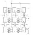
図1に、本発明の一態様に係る半導体装置の構成を、一例として示す。図1に示す半導体
装置は、9つの基本ブロックA乃至基本ブロックIと、それら基本ブロックA乃至基本ブ
ロックI間の接続を制御するプログラム素子SwAB乃至プログラム素子SwIHと、各
基本ブロックA乃至基本ブロックIへの、電源電位VDDの供給を制御するプログラム素
子SwVA乃至プログラム素子SwVIとが設けられている。FIG. 1 shows, as an example, the configuration of a semiconductor device according to one aspect of the present invention. The semiconductor device shown in FIG. 1 includes nine basic blocks A to I, a program element SwAB to a program element SwIH for controlling a connection between the basic blocks A to the basic block I, and each basic block A to the basic block I. A program element SwVA to a program element SwVI that controls the supply of the power supply potential VDD to the device is provided.
なお、図1では、例えば基本ブロックAの出力端子と基本ブロックBの入力端子の接続を
制御するプログラム素子を、SwABと表記する。逆に、基本ブロックBの出力端子と基
本ブロックAの入力端子の接続を制御するプログラム素子を、SwBAと表記する。In FIG. 1, for example, a program element that controls the connection between the output terminal of the basic block A and the input terminal of the basic block B is referred to as SwAB. On the contrary, the program element that controls the connection between the output terminal of the basic block B and the input terminal of the basic block A is referred to as SwBA.
また、図1では、説明の煩雑さを避けるために、9つの各基本ブロックが左右上下のいず
れかの基本ブロックと、プログラム素子を介して接続される場合を例示している。しかし
、本発明はこの構成に限定されず、基本ブロックの数とその接続構造は、設計者が適宜定
めることができる。Further, FIG. 1 illustrates a case where each of the nine basic blocks is connected to one of the left, right, top, and bottom basic blocks via a program element in order to avoid complication of explanation. However, the present invention is not limited to this configuration, and the number of basic blocks and the connection structure thereof can be appropriately determined by the designer.
また、図1では、各基本ブロックが、プログラム素子を介して、電源電位VDDの与えら
れているノードと接続されている構成を示しているが、実際には、各基本ブロックは、電
源電位VDDの他に、電源電位VDDと電位差を有するグラウンドなどの固定電位が与え
られている。すなわち、基本ブロックに電源電位VDDが与えられることで、電源電位V
DDと上記固定電位の電位差が、電源電圧として当該基本ブロックに供給されることとな
る。Further, FIG. 1 shows a configuration in which each basic block is connected to a node to which the power supply potential VDD is given via a program element, but in reality, each basic block is connected to the power supply potential VDD. In addition, a fixed potential such as a ground having a potential difference from the power supply potential VDD is given. That is, by giving the power supply potential VDD to the basic block, the power supply potential V
The potential difference between the DD and the fixed potential is supplied to the basic block as a power supply voltage.
また、図1では、任意の基本ブロックが有する一の出力端子が、他の基本ブロックが有す
る一の入力端子に、それぞれプログラム素子を介して接続されている場合を例示している
。しかし、本発明はこの構成に限定されず、任意の基本ブロックが有する一の出力端子が
、他の基本ブロックが有する複数の入力端子に、それぞれプログラム素子を介して接続さ
れていても良い。Further, FIG. 1 illustrates a case where one output terminal of an arbitrary basic block is connected to one input terminal of another basic block via a program element. However, the present invention is not limited to this configuration, and one output terminal of any basic block may be connected to a plurality of input terminals of another basic block via a program element.
なお、基本ブロックとして用いる論理回路の構成は、特に限定されない。インバータ、A
ND、NAND、NORのような、単純な論理演算を行う論理回路から、加算器、乗算器
、メモリ(例えば、DRAMやSRAM等)、さらには各種演算装置を、基本ブロックと
して用いることができる。The configuration of the logic circuit used as the basic block is not particularly limited. Inverter, A
From logic circuits that perform simple logical operations such as ND, NAND, and NOR, adders, multipliers, memories (for example, DRAM, SRAM, etc.), and various arithmetic units can be used as basic blocks.
また、各プログラム素子は、2つのノード間の接続を制御する第1のトランジスタ(Tr
1)と、当該第1のトランジスタが有するゲート電極への、電位の供給を制御する第2の
トランジスタ(Tr2)とを、少なくとも有している。図2に、プログラム素子の構成例
を具体的に示す。Further, each program element is a first transistor (Tr) that controls the connection between the two nodes.
It has at least 1) and a second transistor (Tr2) that controls the supply of potential to the gate electrode of the first transistor. FIG. 2 shows a concrete example of the configuration of the program element.
図2(A)は、最も単純な構造を有するプログラム素子の一例であり、2つのノード間の
接続を制御する第1のトランジスタ(Tr1)と、当該第1のトランジスタ(Tr1)が
有するゲート電極への、電位の供給を制御する第2のトランジスタ(Tr2)とを有する
。具体的に、第1のトランジスタ(Tr1)が有するソース電極はノードN1に、ドレイ
ン電極はノードN2に接続されている。そして、第2のトランジスタ(Tr2)のソース
電極(Sで示す)とドレイン電極(Dで示す)は、いずれか一方が第1のトランジスタ(
Tr1)のゲート電極に接続されており、他方には第1のトランジスタ(Tr1)のスイ
ッチングを制御するための信号(Sig1)の電位が与えられている。FIG. 2A is an example of a program element having the simplest structure, that is, a first transistor (Tr1) that controls a connection between two nodes and a gate electrode included in the first transistor (Tr1). It has a second transistor (Tr2) that controls the supply of potential to. Specifically, the source electrode of the first transistor (Tr1) is connected to the node N1, and the drain electrode is connected to the node N2. Then, one of the source electrode (indicated by S) and the drain electrode (indicated by D) of the second transistor (Tr2) is the first transistor (indicated by D).
It is connected to the gate electrode of Tr1), and the potential of the signal (Sig1) for controlling the switching of the first transistor (Tr1) is given to the other.
なお、第1のトランジスタ(Tr1)が有するゲート電極の電位を保持するための容量素
子を設けるようにしても良い。It should be noted that a capacitive element for holding the potential of the gate electrode of the first transistor (Tr1) may be provided.
第2のトランジスタ(Tr2)が、そのゲート電極に入力される信号に従ってオンになる
と、第1のトランジスタ(Tr1)のスイッチングを制御するための信号の電位が、第1
のトランジスタ(Tr1)のゲート電極に与えられる。第1のトランジスタ(Tr1)は
、そのゲート電極に与えられた電位に従ってスイッチングを行う。第1のトランジスタ(
Tr1)がオンだと、ノードN1とノードN2が接続される。逆に、第1のトランジスタ
(Tr1)がオフだと、ノードN1とノードN2は接続されず、これらのノードのいずれ
か一方は、ハイインピーダンスの状態となる。When the second transistor (Tr2) is turned on according to the signal input to the gate electrode, the potential of the signal for controlling the switching of the first transistor (Tr1) becomes the first.
It is given to the gate electrode of the transistor (Tr1) of. The first transistor (Tr1) switches according to the potential given to the gate electrode. First transistor (
When Tr1) is on, node N1 and node N2 are connected. On the contrary, when the first transistor (Tr1) is off, the node N1 and the node N2 are not connected, and one of these nodes is in a high impedance state.
次いで、第2のトランジスタ(Tr2)が、そのゲート電極に入力される信号に従ってオ
フになると、第1のトランジスタ(Tr1)が有するゲート電極はフローティングの状態
となり、その電位が保持される。よって、ノードN1とノードN2の間の接続状態は、保
持される。Next, when the second transistor (Tr2) is turned off according to the signal input to the gate electrode, the gate electrode of the first transistor (Tr1) is in a floating state and its potential is maintained. Therefore, the connection state between the node N1 and the node N2 is maintained.
なお、本明細書において接続とは電気的な接続を意味しており、電流、電圧または電位が
、供給可能、或いは伝送可能な状態に相当する。従って、接続している状態とは、直接接
続している状態を必ずしも指すわけではなく、電流、電圧または電位が、供給可能、或い
は伝送可能であるように、配線、抵抗、ダイオード、トランジスタなどの回路素子を介し
て間接的に接続している状態も、その範疇に含む。In the present specification, the connection means an electrical connection, and corresponds to a state in which a current, a voltage, or a potential can be supplied or transmitted. Therefore, the connected state does not necessarily mean the directly connected state, and the wiring, resistance, diode, transistor, etc. so that the current, voltage, or potential can be supplied or transmitted. The state of being indirectly connected via a circuit element is also included in the category.
また、回路図上は独立している構成要素どうしが接続されている場合であっても、実際に
は、例えば配線の一部が電極としても機能する場合など、一の導電膜が、複数の構成要素
の機能を併せ持っているだけの場合もある。本明細書において接続とは、このような、一
の導電膜が、複数の構成要素の機能を併せ持っている場合も、その範疇に含める。Further, even when independent components on the circuit diagram are connected to each other, in reality, one conductive film may have a plurality of electrodes, for example, when a part of the wiring also functions as an electrode. In some cases, it only has the functions of the components. As used herein, the term "connection" includes the case where one conductive film has the functions of a plurality of components in combination.
また、トランジスタが有するソース電極とドレイン電極は、トランジスタの極性及び各電
極に与えられる電位の高低差によって、その呼び方が入れ替わる。一般的に、nチャネル
型トランジスタでは、低い電位が与えられる電極がソース電極と呼ばれ、高い電位が与え
られる電極がドレイン電極と呼ばれる。また、pチャネル型トランジスタでは、低い電位
が与えられる電極がドレイン電極と呼ばれ、高い電位が与えられる電極がソース電極と呼
ばれる。本明細書では、便宜上、ソース電極とドレイン電極が固定されているものと仮定
して、トランジスタの接続関係を説明する場合があるが、実際には上記電位の関係に従っ
てソース電極とドレイン電極の呼び方が入れ替わる。Further, the names of the source electrode and the drain electrode of the transistor are interchanged depending on the polarity of the transistor and the height difference of the potential given to each electrode. Generally, in an n-channel transistor, an electrode to which a low potential is given is called a source electrode, and an electrode to which a high potential is given is called a drain electrode. Further, in the p-channel transistor, the electrode to which a low potential is given is called a drain electrode, and the electrode to which a high potential is given is called a source electrode. In the present specification, for convenience, the connection relationship between the transistors may be described on the assumption that the source electrode and the drain electrode are fixed, but in reality, the source electrode and the drain electrode are referred to according to the above potential relationship. The ones are replaced.
なお、基本ブロック間の接続を制御するプログラム素子の場合、ノードN1とノードN2
は、それぞれ互いに異なる基本ブロックの入力端子または出力端子に接続されている。ま
た、基本ブロックへの電源電圧の供給を制御するプログラム素子の場合、ノードN1とノ
ードN2は、一方が基本ブロックに接続されており、他方には電源電位VDDが与えられ
ている。In the case of a program element that controls the connection between basic blocks, node N1 and node N2
Are connected to the input or output terminals of different basic blocks. Further, in the case of a program element that controls the supply of the power supply voltage to the basic block, one of the node N1 and the node N2 is connected to the basic block, and the other is given the power supply potential VDD.
次いで、図2(B)に、プログラム素子の別の一例を示す。図2(B)に示すプログラム
素子は、2つのノード間の接続を制御する第1のトランジスタ(Tr1)と、当該第1の
トランジスタ(Tr1)が有するゲート電極への、電位の供給を制御する第2のトランジ
スタ(Tr2)と、上記2つのノードのいずれか一つと、固定電位VSSが与えられてい
るノードとの間の接続を制御する第3のトランジスタ(Tr3)とを有する。Next, FIG. 2B shows another example of the program element. The program element shown in FIG. 2B controls the supply of potential to the first transistor (Tr1) that controls the connection between the two nodes and the gate electrode of the first transistor (Tr1). It has a second transistor (Tr2), one of the above two nodes, and a third transistor (Tr3) that controls the connection between the node to which the fixed potential VSS is given.
具体的に、第1のトランジスタ(Tr1)が有するソース電極はノードN1に、ドレイン
電極はノードN2に接続されている。そして、第2のトランジスタ(Tr2)のソース電
極とドレイン電極は、いずれか一方が第1のトランジスタ(Tr1)のゲート電極に接続
されており、他方には第1のトランジスタ(Tr1)のスイッチングを制御するための信
号の電位が与えられている。また、第3のトランジスタ(Tr3)が有するソース電極と
ドレイン電極は、一方がノードN2に接続されており、他方が固定電位VSSの与えられ
ているノードに接続されている。そして、第1のトランジスタ(Tr1)のゲート電極と
、第3のトランジスタ(Tr3)のゲート電極とが接続されている。なお、第1のトラン
ジスタ(Tr1)はnチャネル型トランジスタであり、第3のトランジスタ(Tr3)は
pチャネル型トランジスタである。Specifically, the source electrode of the first transistor (Tr1) is connected to the node N1, and the drain electrode is connected to the node N2. One of the source electrode and the drain electrode of the second transistor (Tr2) is connected to the gate electrode of the first transistor (Tr1), and the other is switched to the first transistor (Tr1). The potential of the signal to control is given. Further, one of the source electrode and the drain electrode of the third transistor (Tr3) is connected to the node N2, and the other is connected to the node to which the fixed potential VSS is given. Then, the gate electrode of the first transistor (Tr1) and the gate electrode of the third transistor (Tr3) are connected to each other. The first transistor (Tr1) is an n-channel transistor, and the third transistor (Tr3) is a p-channel transistor.
また、図2(B)に示すプログラム素子は、第1のトランジスタ(Tr1)が有するゲー
ト電極の電位を保持するための容量素子Csを有している。容量素子Csは必ずしも設け
る必要はないが、容量素子Csを設けることで、ノードN1とノードN2間の接続状態を
、より長い期間に渡って保持することができる。具体的に、容量素子Csが有する一対の
電極は、一方が第1のトランジスタ(Tr1)のゲート電極に接続されており、他方が固
定電位VSSの与えられているノードに接続されている。Further, the program element shown in FIG. 2B has a capacitive element Cs for holding the potential of the gate electrode of the first transistor (Tr1). Although it is not always necessary to provide the capacitive element Cs, by providing the capacitive element Cs, the connection state between the node N1 and the node N2 can be maintained for a longer period of time. Specifically, one of the pair of electrodes of the capacitive element Cs is connected to the gate electrode of the first transistor (Tr1), and the other is connected to a node to which a fixed potential VSS is given.
第2のトランジスタ(Tr2)が、そのゲート電極に入力される信号に従ってオンになる
と、第1のトランジスタ(Tr1)のスイッチングを制御するための信号の電位が、第1
のトランジスタ(Tr1)のゲート電極と、第3のトランジスタ(Tr3)のゲート電極
と、容量素子Csの一方の電極に与えられる。第1のトランジスタ(Tr1)は、そのゲ
ート電極に与えられた信号の電位に従ってスイッチングを行う。そして、第3のトランジ
スタ(Tr3)は、第1のトランジスタ(Tr1)と極性が異なるので、第1のトランジ
スタ(Tr1)と逆のスイッチングを行う。When the second transistor (Tr2) is turned on according to the signal input to the gate electrode, the potential of the signal for controlling the switching of the first transistor (Tr1) becomes the first.
It is given to the gate electrode of the transistor (Tr1), the gate electrode of the third transistor (Tr3), and one electrode of the capacitive element Cs. The first transistor (Tr1) switches according to the potential of the signal given to the gate electrode. Since the third transistor (Tr3) has a different polarity from that of the first transistor (Tr1), the switching is reversed from that of the first transistor (Tr1).
例えば、第1のトランジスタ(Tr1)がオンになると、第3のトランジスタ(Tr3)
はオフとなる。その結果、ノードN1とノードN2が接続される。逆に、第1のトランジ
スタ(Tr1)がオフになると、第3のトランジスタ(Tr3)はオンとなる。その結果
、ノードN1とノードN2は接続されず、ノードN2が、固定電位VSSの与えられてい
るノードに接続される。For example, when the first transistor (Tr1) is turned on, the third transistor (Tr3)
Is turned off. As a result, node N1 and node N2 are connected. Conversely, when the first transistor (Tr1) is turned off, the third transistor (Tr3) is turned on. As a result, the node N1 and the node N2 are not connected, and the node N2 is connected to the node to which the fixed potential VSS is given.
次いで、第2のトランジスタ(Tr2)が、そのゲート電極に入力される信号に従ってオ
フになると、第1のトランジスタ(Tr1)が有するゲート電極と、第3のトランジスタ
(Tr3)が有するゲート電極はフローティングの状態となり、その電位が容量Csによ
り保持される。よって、ノードN1とノードN2の間と、ノードN2と固定電位VSSの
与えられているノードの間の接続状態は、保持される。Then, when the second transistor (Tr2) is turned off according to the signal input to the gate electrode, the gate electrode of the first transistor (Tr1) and the gate electrode of the third transistor (Tr3) are floating. , And the potential is held by the capacitance Cs. Therefore, the connection state between the node N1 and the node N2 and between the node N2 and the node to which the fixed potential VSS is given is maintained.
なお、図2(B)では、第3のトランジスタ(Tr3)に、pチャネル型トランジスタを
用いたが、酸化物半導体のように一般的にpチャネル型が得られない、あるいは、得られ
たとしても移動度が非常に低い場合には、図2(C)で示すように、pチャネル型トラン
ジスタの代わりに抵抗Rを用いることもできる。In FIG. 2B, a p-channel type transistor was used for the third transistor (Tr3), but it is assumed that the p-channel type cannot be generally obtained or is obtained as in the case of oxide semiconductors. If the mobility is very low, a resistor R can be used instead of the p-channel transistor, as shown in FIG. 2C.
そして、本発明の一態様では、図2(A)乃至図2(C)に例示したプログラム素子にお
いて、第2のトランジスタ(Tr2)のオフ電流またはリーク電流が極めて低いことを特
徴とする。具体的に、第2のトランジスタ(Tr2)は、シリコン半導体よりもバンドギ
ャップが広く、真性キャリア密度がシリコンよりも低い半導体材料を、チャネル形成領域
に含むことを特徴とするものである。上述したような特性を有する半導体材料をチャネル
形成領域に含むことで、オフ電流が極めて低いトランジスタを実現することができる。One aspect of the present invention is characterized in that the off-current or leak current of the second transistor (Tr2) is extremely low in the program elements exemplified in FIGS. 2 (A) to 2 (C). Specifically, the second transistor (Tr2) is characterized in that a semiconductor material having a wider bandgap than a silicon semiconductor and a lower intrinsic carrier density than silicon is included in the channel forming region. By including the semiconductor material having the above-mentioned characteristics in the channel forming region, a transistor having an extremely low off-current can be realized.
シリコン半導体よりもバンドギャップが広く、真性キャリア密度がシリコンよりも低い半
導体材料の一例として、炭化珪素(SiC)、窒化ガリウム(GaN)などの化合物半導
体、酸化亜鉛(ZnO)などの金属酸化物でなる酸化物半導体などを適用することができ
る。この中でも酸化物半導体は、スパッタリング法や湿式法(印刷法など)により作製可
能であり、量産性に優れるといった利点がある。また、炭化珪素や窒化ガリウムは単結晶
としなければ十分な特性が得られず、そのための炭化珪素のプロセス温度は約1500℃
、窒化ガリウムのプロセス温度は約1100℃であるが、酸化物半導体の成膜温度は、3
00~500℃(最大でも700℃程度)と低く、単結晶シリコン等の半導体材料を用い
た集積回路上に、酸化物半導体による半導体素子を積層させることも可能である。また、
基板の大型化にも対応が可能である。よって、上述したワイドギャップ半導体の中でも、
特に酸化物半導体は量産性が高いというメリットを有する。また、より優れた性能(例え
ば電界効果移動度)を有する結晶性の酸化物半導体も、450℃から800℃の熱処理に
よって容易に得ることができる。As an example of a semiconductor material having a wider band gap than a silicon semiconductor and a lower intrinsic carrier density than silicon, compound semiconductors such as silicon carbide (SiC) and gallium nitride (GaN), and metal oxides such as zinc oxide (ZnO) are used. Oxide semiconductors and the like can be applied. Among these, oxide semiconductors can be manufactured by a sputtering method or a wet method (printing method, etc.), and have an advantage of being excellent in mass productivity. Further, silicon carbide and gallium nitride cannot obtain sufficient characteristics unless they are made into a single crystal, and the process temperature of silicon carbide for that purpose is about 1500 ° C.
, The process temperature of gallium nitride is about 1100 ° C., but the film formation temperature of the oxide semiconductor is 3.
It is as low as 00 to 500 ° C. (up to about 700 ° C.), and it is also possible to laminate a semiconductor element made of an oxide semiconductor on an integrated circuit using a semiconductor material such as single crystal silicon. again,
It is also possible to handle larger boards. Therefore, among the wide-gap semiconductors mentioned above,
In particular, oxide semiconductors have the advantage of high mass productivity. Further, a crystalline oxide semiconductor having better performance (for example, field effect mobility) can be easily obtained by heat treatment at 450 ° C. to 800 ° C.
酸化物半導体を第2のトランジスタ(Tr2)に用いる場合、上記酸化物半導体は、バン
ドギャップが3eV以上でかつ、キャリア密度が1012/cm3未満、好ましくは10
11/cm3未満の特性を有することが望ましい。また、上記酸化物半導体は、SIMS
による水素濃度の測定値が、5×10¹⁹/cm3以下、好ましくは5×1018/cm
3以下、より好ましくは5×10¹⁷/cm3以下、さらに好ましくは1×1016/c
m3以下であることが望ましい。上記特性を有する酸化物半導体を用いることで、第2の
トランジスタ(Tr2)のオフ電流、リーク電流を低くすることができる。When the oxide semiconductor is used for the second transistor (Tr2), the oxide semiconductor has a bandgap of 3 eV or more and a carrier density of less than 1012 / cm3 , preferably 10.
It is desirable to have a characteristic of less than11 /cm3 . The oxide semiconductor is SIMS.
The measured value of hydrogen concentration by 5 × 10¹⁹ / cm3 or less, preferably 5 × 10¹⁸ / cm.
3 or less, more preferably 5 × 10¹⁷ / cm3 or less, still more preferably 1 × 10¹⁶ / c
It is desirable that it is m3 or less. By using an oxide semiconductor having the above characteristics, the off current and leakage current of the second transistor (Tr2) can be reduced.
また、第2のトランジスタ(Tr2)は、ゲート絶縁膜の厚さが、10nm以上、好まし
くは、100nm以上とするのが望ましく、また、チャネル長を100nm以上、好まし
くは300nm以上とするのが望ましい。上記構造を採用することで、第2のトランジス
タ(Tr2)のオフ電流、リーク電流を低くすることができる。The thickness of the gate insulating film of the second transistor (Tr2) is preferably 10 nm or more, preferably 100 nm or more, and the channel length is preferably 100 nm or more, preferably 300 nm or more. .. By adopting the above structure, the off current and leakage current of the second transistor (Tr2) can be reduced.
このように、オフ電流、リーク電流の著しく低い第2のトランジスタ(Tr2)を用いて
、第1のトランジスタが有するゲート電極への電位の供給を制御することで、第1のトラ
ンジスタのゲート電圧は、長期間に渡って保持される。従って、ノードN1とノードN2
の間の接続状態も、長期間に渡り保持することができる。In this way, by controlling the supply of potential to the gate electrode of the first transistor by using the second transistor (Tr2) having extremely low off current and leakage current, the gate voltage of the first transistor can be adjusted. , Retained for a long period of time. Therefore, node N1 and node N2
The connection state between them can also be maintained for a long period of time.
なお、接続状態を保持する際において、第2のトランジスタ(Tr2)のオフ電流、リー
ク電流をさらに低減させるには、第2のトランジスタ(Tr2)が有するゲート電極の電
位を、プログラム素子の中で最も低くなるように設定すればよい。具体的には、トランジ
スタ、容量素子、抵抗などの、プログラム素子を構成する全ての回路素子が有する電極や
端子の電位のうち、第2のトランジスタ(Tr2)が有するゲート電極の電位が、他の全
ての電位よりも3V以上、より好ましくは5V以上低くなるように設定するのが望ましい
。In order to further reduce the off current and leakage current of the second transistor (Tr2) when maintaining the connected state, the potential of the gate electrode of the second transistor (Tr2) is set in the program element. It should be set to be the lowest. Specifically, among the potentials of the electrodes and terminals of all the circuit elements constituting the program element such as the transistor, the capacitive element, and the resistor, the potential of the gate electrode of the second transistor (Tr2) is the other potential. It is desirable to set it so that it is 3 V or more, more preferably 5 V or more lower than all the potentials.
また、第1のトランジスタ(Tr1)または第3のトランジスタ(Tr3)は、第2のト
ランジスタ(Tr2)と同様に、シリコン半導体よりもバンドギャップが広く、真性キャ
リア密度がシリコンよりも低い半導体材料をチャネル形成領域に有していても良いし、第
2のトランジスタ(Tr2)とは異なり、移動度のより高い半導体材料をチャネル形成領
域に有していても良い。移動度の高い半導体材料として、例えば、多結晶や単結晶などの
結晶性を有するゲルマニウム、シリコン、シリコンゲルマニウムや、単結晶炭化珪素など
が適している。また、第1のトランジスタ(Tr1)または第3のトランジスタ(Tr3
)は、薄膜の半導体膜を用いていても良いし、バルクの半導体基板を用いていても良い。Further, the first transistor (Tr1) or the third transistor (Tr3), like the second transistor (Tr2), is a semiconductor material having a wider bandgap than a silicon semiconductor and a lower intrinsic carrier density than silicon. It may be contained in the channel forming region, or unlike the second transistor (Tr2), the semiconductor material having higher mobility may be contained in the channel forming region. As the semiconductor material having high mobility, for example, germanium having crystallinity such as polycrystal or single crystal, silicon, silicon germanium, single crystal silicon carbide and the like are suitable. Further, the first transistor (Tr1) or the third transistor (Tr3).
) May use a thin-film semiconductor film or a bulk semiconductor substrate.
前者の場合、第1のトランジスタ(Tr1)または第3のトランジスタ(Tr3)も第2
のトランジスタ(Tr2)と同様に、オフ電流、リーク電流が低いという特性を有するこ
とになるので、半導体装置の消費電力をさらに削減することができる。特に、基本ブロッ
クへの電源電位VDDの供給を制御するプログラム素子の場合、第1のトランジスタ(T
r1)の電界効果移動度が10cm2V-1s-1程度であれば十分動作が可能であり、
さほど高い動作速度は要求されない。そして、基本ブロックへの電源電位VDDの供給を
制御するプログラム素子において生じるオフ電流、リーク電流は、消費電力の増大にその
まま繋がってしまう。そのため、基本ブロックへの電源電位VDDの供給を制御するプロ
グラム素子の場合は、前者の構成を採用することが望ましい。In the former case, the first transistor (Tr1) or the third transistor (Tr3) is also the second.
Similar to the transistor (Tr2) of No. 1, it has the characteristics of low off-current and low leakage current, so that the power consumption of the semiconductor device can be further reduced. In particular, in the case of a program element that controls the supply of the power supply potential VDD to the basic block, the first transistor (T).
If the electric field effect mobility of r1) is about 10 cm2 V-1 s-1 , sufficient operation is possible.
Not very high operating speed is required. The off-current and leak current generated in the program element that controls the supply of the power supply potential VDD to the basic block directly leads to an increase in power consumption. Therefore, in the case of a program element that controls the supply of the power supply potential VDD to the basic block, it is desirable to adopt the former configuration.
また、後者の場合、第1のトランジスタ(Tr1)の移動度が高くなるので、第1のトラ
ンジスタ(Tr1)によって接続されるノード間の抵抗を低くすることができる。特に、
基本ブロック間の接続を制御するためのプログラム素子の場合、基本ブロックどうしの接
続抵抗が高いことは、半導体装置の動作速度の低減につながる。そのため、基本ブロック
間の接続を制御するためのプログラム素子の場合は、後者の構成を採用することが望まし
い。なお、第1のトランジスタ(Tr1)が移動度のより高い半導体材料をチャネル形成
領域に有している場合において、オフ電流、リーク電流を低減させるには、そのゲート絶
縁膜の厚さを10nm以上とすることが好ましい。Further, in the latter case, since the mobility of the first transistor (Tr1) is increased, the resistance between the nodes connected by the first transistor (Tr1) can be reduced. especially,
In the case of a program element for controlling the connection between basic blocks, a high connection resistance between the basic blocks leads to a reduction in the operating speed of the semiconductor device. Therefore, in the case of a program element for controlling the connection between basic blocks, it is desirable to adopt the latter configuration. When the first transistor (Tr1) has a semiconductor material having higher mobility in the channel forming region, in order to reduce the off-current and leakage current, the thickness of the gate insulating film is 10 nm or more. Is preferable.
なお、第2のトランジスタ(Tr2)と、第1のトランジスタ(Tr1)及び第3のトラ
ンジスタ(Tr3)とが、同じ半導体材料をチャネル形成領域に有している場合、第1の
トランジスタ(Tr1)及び第3のトランジスタ(Tr3)を第2のトランジスタ(Tr
2)と同じ層内に形成してもよい。この場合、第1のトランジスタ(Tr1)及び第3の
トランジスタ(Tr3)と、第2のトランジスタ(Tr2)とは、ゲート絶縁膜の膜厚が
設計上同じとなるが、チャネル長、またはチャネル幅は、異ならせておいても良い。例え
ば、第1のトランジスタ(Tr1)のチャネル形成領域を低抵抗にしたい場合、そのチャ
ネル幅を、第2のトランジスタ(Tr2)の2倍以上、好ましくは5倍以上とすると良い
。When the second transistor (Tr2), the first transistor (Tr1), and the third transistor (Tr3) have the same semiconductor material in the channel forming region, the first transistor (Tr1) And the third transistor (Tr3) is replaced with the second transistor (Tr).
It may be formed in the same layer as 2). In this case, the first transistor (Tr1) and the third transistor (Tr3) and the second transistor (Tr2) have the same gate insulating film thickness by design, but the channel length or channel width is the same. May be different. For example, when it is desired to reduce the resistance of the channel forming region of the first transistor (Tr1), the channel width may be twice or more, preferably five times or more that of the second transistor (Tr2).
さらに、第1のトランジスタ(Tr1)は、ノンセルフアライン方式で作製してもよい。
ノンセルフアライン方式では、ゲート電極と、ソース電極またはドレイン電極とのオーバ
ーラップによる寄生容量が生じるが、第1のトランジスタ(Tr1)は高速動作をさほど
要求されないので、上記寄生容量は問題とならない。むしろ、上記寄生容量は、第1のト
ランジスタ(Tr1)のゲート電極の電位を保持する容量(Cs)として機能する。他方
、第2のトランジスタ(Tr2)は、スイッチングの際に第1のトランジスタ(Tr1)
のゲート電極に電位の変化が発生するのを防ぐために、その寄生容量は小さいことが好ま
しい。Further, the first transistor (Tr1) may be manufactured by a non-self-alignment method.
In the non-self-aligned method, a parasitic capacitance is generated due to the overlap between the gate electrode and the source electrode or the drain electrode, but since the first transistor (Tr1) is not required to operate at high speed so much, the parasitic capacitance does not matter. Rather, the parasitic capacitance functions as a capacitance (Cs) that holds the potential of the gate electrode of the first transistor (Tr1). On the other hand, the second transistor (Tr2) is the first transistor (Tr1) during switching.
It is preferable that the parasitic capacitance is small in order to prevent a change in potential from occurring in the gate electrode of.
また、第1のトランジスタ(Tr1)に、基本ブロックを構成するトランジスタと同じ半
導体材料を用いる場合であっても、第1のトランジスタ(Tr1)のリーク電流を低減す
るために、そのゲート絶縁膜の膜厚は、基本ブロックを構成するトランジスタよりも大き
いことが望ましい。この場合、第1のトランジスタ(Tr1)は、上述したノンセルフア
ライン方式で作製し、基本ブロックに用いられるトランジスタとは異なる層に形成された
導電膜を、そのゲート電極として用いても良い。Further, even when the same semiconductor material as the transistor constituting the basic block is used for the first transistor (Tr1), in order to reduce the leakage current of the first transistor (Tr1), the gate insulating film thereof is used. It is desirable that the film thickness is larger than that of the transistors constituting the basic block. In this case, the first transistor (Tr1) may be manufactured by the above-mentioned non-self-alignment method, and a conductive film formed in a layer different from the transistor used for the basic block may be used as the gate electrode thereof.
なお、図2では、第1のトランジスタ(Tr1)、第2のトランジスタ(Tr2)、第3
のトランジスタ(Tr3)が、ゲート電極を半導体膜の片側にのみ有している場合を示し
ている。しかし、本発明の一態様はこの構成に限定されず、上記トランジスタが、半導体
膜を間に挟んでゲート電極の反対側に存在するバックゲート電極を有していても良い。こ
の場合、バックゲート電極は、電気的に絶縁しているフローティングの状態であっても良
いし、電位が他から与えられている状態であっても良い。後者の場合、ゲート電極とバッ
クゲート電極が電気的に接続されていても良いし、バックゲート電極にのみ、常にグラウ
ンドなどの固定電位が与えられていても良い。バックゲート電極に与える電位の高さを制
御することで、トランジスタの閾値電圧を制御することができる。In FIG. 2, the first transistor (Tr1), the second transistor (Tr2), and the third transistor are shown.
The transistor (Tr3) of the above shows the case where the gate electrode is provided only on one side of the semiconductor film. However, one aspect of the present invention is not limited to this configuration, and the transistor may have a back gate electrode existing on the opposite side of the gate electrode with a semiconductor film in between. In this case, the back gate electrode may be in a floating state in which it is electrically insulated, or may be in a state in which a potential is given from another. In the latter case, the gate electrode and the back gate electrode may be electrically connected, or a fixed potential such as ground may always be applied only to the back gate electrode. By controlling the height of the potential applied to the back gate electrode, the threshold voltage of the transistor can be controlled.
また、半導体装置に用いることができるプログラム素子は、図2に示した回路構成に限定
されず、少なくとも、2つのノード間の接続を制御するための第1のトランジスタと、上
記第1のトランジスタが有するゲート電極への、電位の供給を制御するための第2のトラ
ンジスタとを有し、なおかつ、第2のトランジスタが、シリコンの約3倍程度の大きなバ
ンドギャップを有する酸化物半導体などの半導体材料をチャネル形成領域に有していれば
良い。Further, the program element that can be used in the semiconductor device is not limited to the circuit configuration shown in FIG. 2, and at least the first transistor for controlling the connection between the two nodes and the first transistor are used. A semiconductor material such as an oxide semiconductor having a second transistor for controlling the supply of potential to the gate electrode, and the second transistor having a large band gap of about 3 times that of silicon. It suffices to have in the channel formation region.
次いで、上述した構成を有するプログラム素子を用いて、複数の基本ブロックを任意に接
続する場合の、半導体装置の動作について説明する。Next, the operation of the semiconductor device when a plurality of basic blocks are arbitrarily connected by using the program element having the above-described configuration will be described.
図1に示す半導体装置では、全ての基本ブロック間の接続が切断され、また、全ての基本
ブロックへの電源電圧の供給が停止している状態である。この図1に示す状態から、プロ
グラム素子の幾つかをオンとして、基本ブロック間が接続された状態を、図3に示す。具
体的に、図3では、プログラム素子SwAB、プログラム素子SwBC、プログラム素子
SwCF、プログラム素子SwFIがオンになることで、基本ブロックAの出力端子と基
本ブロックBの入力端子が接続され、基本ブロックBの出力端子と基本ブロックCの入力
端子が接続され、基本ブロックCの出力端子と基本ブロックFの入力端子が接続され、基
本ブロックFの出力端子と基本ブロックIの入力端子が接続されている。また、プログラ
ム素子SwVA、プログラム素子SwVB、プログラム素子SwVC、プログラム素子S
wVF、プログラム素子SwVIがオンになることで、基本ブロックA、基本ブロックB
、基本ブロックC、基本ブロックF、基本ブロックIに、電源電位VDDが与えられてい
る。そして、上記以外の全てのプログラム素子はオフになっている。この結果、図3に示
すように、半導体装置の入力端子(IN)から、基本ブロックA-基本ブロックB-基本
ブロックC-基本ブロックF-基本ブロックIという信号の経路が形成される。そして、
上記各基本ブロックにおいて第1の信号処理が行われることにより、出力端子(OUT)
から信号が出力される。In the semiconductor device shown in FIG. 1, the connection between all the basic blocks is disconnected, and the supply of the power supply voltage to all the basic blocks is stopped. From the state shown in FIG. 1, a state in which some of the program elements are turned on and the basic blocks are connected is shown in FIG. Specifically, in FIG. 3, when the program element SwAB, the program element SwBC, the program element SwCF, and the program element SwFI are turned on, the output terminal of the basic block A and the input terminal of the basic block B are connected, and the basic block B is connected. The output terminal of the basic block C and the input terminal of the basic block C are connected, the output terminal of the basic block C and the input terminal of the basic block F are connected, and the output terminal of the basic block F and the input terminal of the basic block I are connected. Further, the program element SwVA, the program element SwVB, the program element SwVC, and the program element S.
When wVF and the program element SwVI are turned on, basic block A and basic block B are turned on.
, Basic block C, basic block F, and basic block I are given a power supply potential VDD. And all the program elements other than the above are turned off. As a result, as shown in FIG. 3, a signal path of basic block A-basic block B-basic block C-basic block F-basic block I is formed from the input terminal (IN) of the semiconductor device. and,
By performing the first signal processing in each of the above basic blocks, the output terminal (OUT)
The signal is output from.
なお、この図3に示した状態で、入力された信号に第1の信号処理を施して出力信号を得
た後に、第2の信号処理を行う場合には、基本ブロック間の接続を変更する。基本ブロッ
ク間の接続の変更は、一旦、全てのプログラム素子を切断した後に行うことが望ましい。In the state shown in FIG. 3, when the input signal is subjected to the first signal processing to obtain the output signal and then the second signal processing is performed, the connection between the basic blocks is changed. .. It is desirable to change the connection between the basic blocks once after disconnecting all the program elements.
第2の信号処理を行う際の、基本ブロック間の接続状態の一例を、図4に示す。具体的に
、図4では、プログラム素子SwAD、プログラム素子SwDE、プログラム素子SwE
H、プログラム素子SwHIがオンになることで、基本ブロックAの出力端子と基本ブロ
ックDの入力端子が接続され、基本ブロックDの出力端子と基本ブロックEの入力端子が
接続され、基本ブロックEの出力端子と基本ブロックHの入力端子が接続され、基本ブロ
ックHの出力端子と基本ブロックIの入力端子が接続されている。また、プログラム素子
SwVA、プログラム素子SwVD、プログラム素子SwVE、プログラム素子SwVH
、プログラム素子SwVIがオンになることで、基本ブロックA、基本ブロックD、基本
ブロックE、基本ブロックH、基本ブロックIに、電源電位VDDが与えられている。そ
して、上記以外の全てのプログラム素子はオフになっている。この結果、図4に示すよう
に、半導体装置の入力端子(IN)から、基本ブロックA-基本ブロックD-基本ブロッ
クE-基本ブロックH-基本ブロックIという信号の経路が形成される。そして、上記各
基本ブロックにおいて第2の信号処理が行われることにより、出力端子(OUT)から信
号が出力される。FIG. 4 shows an example of the connection state between the basic blocks when the second signal processing is performed. Specifically, in FIG. 4, the program element SwAD, the program element SwDE, and the program element SwE
H, When the program element SwHI is turned on, the output terminal of the basic block A and the input terminal of the basic block D are connected, the output terminal of the basic block D and the input terminal of the basic block E are connected, and the basic block E is connected. The output terminal and the input terminal of the basic block H are connected, and the output terminal of the basic block H and the input terminal of the basic block I are connected. Further, the program element SwVA, the program element SwVD, the program element SwVE, and the program element SwVH.
When the program element SwVI is turned on, the power supply potential VDD is given to the basic block A, the basic block D, the basic block E, the basic block H, and the basic block I. And all the program elements other than the above are turned off. As a result, as shown in FIG. 4, a signal path of basic block A-basic block D-basic block E-basic block H-basic block I is formed from the input terminal (IN) of the semiconductor device. Then, a signal is output from the output terminal (OUT) by performing the second signal processing in each of the basic blocks.
さらに、第3の信号処理を行う場合も、一旦、全てのプログラム素子を切断した後に、基
本ブロック間の接続の変更を行うことが望ましい。第3の信号処理を行う際の、基本ブロ
ック間の接続状態の一例を、図5に示す。具体的に、図5では、プログラム素子SwAD
、プログラム素子SwDG、プログラム素子SwGH、プログラム素子SwHE、プログ
ラム素子SwEF、プログラム素子SwFIがオンになることで、基本ブロックAの出力
端子と基本ブロックDの入力端子が接続され、基本ブロックDの出力端子と基本ブロック
Gの入力端子が接続され、基本ブロックGの出力端子と基本ブロックHの入力端子が接続
され、基本ブロックHの出力端子と基本ブロックEの入力端子が接続され、基本ブロック
Eの出力端子と基本ブロックFの入力端子が接続され、基本ブロックFの出力端子と基本
ブロックIの入力端子が接続されている。また、プログラム素子SwVA、プログラム素
子SwVD、プログラム素子SwVG、プログラム素子SwVH、プログラム素子SwV
E、プログラム素子SwVF、プログラム素子SwVIがオンになることで、基本ブロッ
クA、基本ブロックD、基本ブロックE、基本ブロックF、基本ブロックG、基本ブロッ
クH、基本ブロックIに、電源電位VDDが与えられている。そして、上記以外の全ての
プログラム素子はオフになっている。この結果、図5に示すように、半導体装置の入力端
子(IN)から、基本ブロックA-基本ブロックD-基本ブロックG―基本ブロックH-
基本ブロックE-基本ブロックF-基本ブロックIという信号の経路が形成される。そし
て、上記各基本ブロックにおいて第3の信号処理が行われることにより、出力端子(OU
T)から信号が出力される。Further, also when performing the third signal processing, it is desirable to change the connection between the basic blocks after disconnecting all the program elements once. FIG. 5 shows an example of the connection state between the basic blocks when the third signal processing is performed. Specifically, in FIG. 5, the program element SwAD
By turning on the program element SwDG, the program element SwGH, the program element SwHE, the program element SwEF, and the program element SwFI, the output terminal of the basic block A and the input terminal of the basic block D are connected, and the output terminal of the basic block D is connected. And the input terminal of the basic block G are connected, the output terminal of the basic block G and the input terminal of the basic block H are connected, the output terminal of the basic block H and the input terminal of the basic block E are connected, and the output of the basic block E is connected. The terminal and the input terminal of the basic block F are connected, and the output terminal of the basic block F and the input terminal of the basic block I are connected. Further, the program element SwVA, the program element SwVD, the program element SwVG, the program element SwVH, and the program element SwV.
When E, the program element SwVF, and the program element SwVI are turned on, the power supply potential VDD is given to the basic block A, the basic block D, the basic block E, the basic block F, the basic block G, the basic block H, and the basic block I. Has been done. And all the program elements other than the above are turned off. As a result, as shown in FIG. 5, from the input terminal (IN) of the semiconductor device, the basic block A-basic block D-basic block G-basic block H-
A signal path called basic block E-basic block F-basic block I is formed. Then, by performing the third signal processing in each of the above basic blocks, the output terminal (OU) is performed.
A signal is output from T).
なお、コンフィギュレーション処理を行う(プログラム素子のスイッチングを制御するこ
とで回路を構築する)のに要する時間は、基本ブロックとプログラム素子で構成されるマ
トリクスの規模にもよるが、図3に示すような回路構成を用いる限りは無視できる程度の
短い時間である。例えば、1行の基本ブロックあたりに要する上記時間は100ナノ秒以
下である。図1のような、3行の基本ブロックで構成されるマトリクスであれば、1マイ
クロ秒もかからない。The time required for performing the configuration process (constructing a circuit by controlling the switching of the program element) depends on the scale of the matrix composed of the basic block and the program element, but is as shown in FIG. It is a short time that can be ignored as long as a simple circuit configuration is used. For example, the time required for one basic block is 100 nanoseconds or less. A matrix composed of three basic blocks as shown in FIG. 1 takes less than 1 microsecond.
本発明の一態様では、回路構成に寄与しない基本ブロックへの電源電圧の供給を停止する
ことにより、半導体装置の消費電力を低く抑えることができる。特に、チャネル長50n
m以下の半導体装置においては、ゲート絶縁膜の厚さが数nm以下となり、消費電力の相
当部分をゲート絶縁膜におけるリーク電流が占めるため、上記構成は消費電力低減のため
に有効である。In one aspect of the present invention, the power consumption of the semiconductor device can be kept low by stopping the supply of the power supply voltage to the basic block that does not contribute to the circuit configuration. In particular, the channel length is 50n
In a semiconductor device of m or less, the thickness of the gate insulating film is several nm or less, and the leakage current in the gate insulating film occupies a considerable part of the power consumption. Therefore, the above configuration is effective for reducing the power consumption.
また、本発明の一態様では、基本ブロックどうしの接続を、オフ電流又はリーク電流の極
めて低いトランジスタにより制御することで、電源電圧が供給されている基本ブロックと
、電源電圧が供給されていない基本ブロックの間に流れるリーク電流またはオフ電流を低
減し、半導体装置の消費電力を低く抑えることができる。Further, in one aspect of the present invention, the connection between the basic blocks is controlled by a transistor having an extremely low off current or leakage current, so that the basic block to which the power supply voltage is supplied and the basic block to which the power supply voltage is not supplied are used. The leakage current or off current flowing between the blocks can be reduced, and the power consumption of the semiconductor device can be kept low.
また、上記構成を有するプログラム素子は、トンネル電流によるゲート絶縁膜の劣化を、
従来のEEPROMを用いたプログラム素子に比べて抑えることができるので、データの
書き換え回数を増やすことができる半導体装置を提供することができる。Further, the program element having the above configuration deteriorates the gate insulating film due to the tunnel current.
Since it can be suppressed as compared with the program element using the conventional EEPROM, it is possible to provide a semiconductor device capable of increasing the number of times of data rewriting.
また、上記構成を有するプログラム素子は、データの書き込みに必要な動作電圧が、第2
のトランジスタ(Tr2)の動作電圧によりほぼ決まる。よって、従来のEEPROMを
用いたプログラム素子に比べて、上記動作電圧を格段に低くすることができ、消費電力を
抑えられる半導体装置を提供することができる。Further, in the program element having the above configuration, the operating voltage required for writing data is second.
It is almost determined by the operating voltage of the transistor (Tr2) of. Therefore, as compared with the conventional programming element using EEPROM, the operating voltage can be remarkably lowered, and a semiconductor device capable of suppressing power consumption can be provided.
また、上記構成を有するプログラム素子は、SRAMを用いたプログラム素子と異なり、
プログラム素子への電源電圧の供給を常時行わなくとも、接続状態をある程度維持するこ
とが可能である。また、オフ電流の著しく低いトランジスタを用いてデータの保持を行っ
ている。そのため、消費電力を抑えられる半導体装置を提供することができる。Further, the program element having the above configuration is different from the program element using SRAM.
It is possible to maintain the connection state to some extent without constantly supplying the power supply voltage to the program element. In addition, data is retained using a transistor with a significantly low off-current. Therefore, it is possible to provide a semiconductor device capable of suppressing power consumption.
(実施の形態2)
実施の形態1では、任意の基本ブロックが、多い場合に4つの隣接する基本ブロックと接
続できる例を示したが、本実施の形態では、任意の基本ブロックが8つの隣接する基本ブ
ロックと接続する例について説明する。(Embodiment 2)
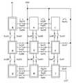
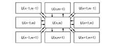
In the first embodiment, an example is shown in which an arbitrary basic block can be connected to four adjacent basic blocks in many cases, but in the present embodiment, the arbitrary basic block is connected to eight adjacent basic blocks. An example will be described.
図6に示す半導体装置には、図1と同様に、9つの基本ブロックA乃至基本ブロックIと
、それら基本ブロックA乃至基本ブロックI間の接続を制御するプログラム素子と、各基
本ブロックA乃至基本ブロックIへの、電源電位VDDの供給を制御するプログラム素子
とが設けられている。Similar to FIG. 1, the semiconductor device shown in FIG. 6 includes nine basic blocks A to basic blocks I, a program element for controlling the connection between these basic blocks A to basic blocks I, and each basic block A to basic blocks A to basic blocks. A program element for controlling the supply of the power supply potential VDD to the block I is provided.
ただし、図6に示す半導体装置は、図1とは異なり、中央の基本ブロックEと、当該基本
ブロックE以外の全ての基本ブロックとが、プログラム素子SwAE乃至プログラム素子
SwIE、プログラム素子SwEA乃至プログラム素子SwEIにより、接続可能である
。However, in the semiconductor device shown in FIG. 6, unlike FIG. 1, the central basic block E and all the basic blocks other than the basic block E are the program element SwAE to the program element SwIE, and the program element SwEA to the program element. It is possible to connect by SwEI.
なお、図6では、中央の基本ブロックEと、その他の基本ブロックの間の接続を制御する
プログラム素子SwAE乃至プログラム素子SwIE、プログラム素子SwEA乃至プロ
グラム素子SwEIと、基本ブロックEへの電源電位VDDの供給を制御するプログラム
素子SwVEのみを示している。しかし、基本ブロックAと基本ブロックB、基本ブロッ
クBと基本ブロックC、基本ブロックCと基本ブロックF、基本ブロックFと基本ブロッ
クI、基本ブロックAと基本ブロックD、基本ブロックDと基本ブロックG、基本ブロッ
クGと基本ブロックH、基本ブロックHと基本ブロックIの間の接続も、図1の場合と同
様に、プログラム素子により制御することができる。また、基本ブロックA、基本ブロッ
クB、基本ブロックC、基本ブロックD、基本ブロックF、基本ブロックG、基本ブロッ
クH、基本ブロックIへの、電源電位VDDの供給も、図1と同様に、プログラム素子に
より制御することが可能である。In FIG. 6, the program element SwAE to the program element SwIE, the program element SwEA to the program element SwEI, and the power supply potential VDD to the basic block E, which control the connection between the central basic block E and the other basic blocks, are shown. Only the program element SwVE that controls the supply is shown. However, basic block A and basic block B, basic block B and basic block C, basic block C and basic block F, basic block F and basic block I, basic block A and basic block D, basic block D and basic block G, The connection between the basic block G and the basic block H, and the connection between the basic block H and the basic block I can also be controlled by the programming element as in the case of FIG. Further, the supply of the power supply potential VDD to the basic block A, the basic block B, the basic block C, the basic block D, the basic block F, the basic block G, the basic block H, and the basic block I is also programmed in the same manner as in FIG. It can be controlled by an element.
なお、プログラム素子は、実施の形態1に示した構成を用いることができる。As the program element, the configuration shown in the first embodiment can be used.
図6に示すように、任意の基本ブロックと接続可能な基本ブロックの数は、設計者が適宜
設定することが可能である。As shown in FIG. 6, the number of basic blocks that can be connected to any basic block can be appropriately set by the designer.
本実施の形態は、上記実施の形態と適宜組み合わせて実施することが可能である。This embodiment can be implemented in combination with the above embodiment as appropriate.
(実施の形態3)
基本ブロックにより大規模なマトリクスが構成されている半導体装置について、より一般
化した例を挙げて、説明する。(Embodiment 3)
A more generalized example of a semiconductor device in which a large-scale matrix is composed of basic blocks will be described.
本実施の形態では、半導体装置が有する、第n行第m列の基本ブロックU(n,m)に注
目する。図7に示すように、基本ブロックU(n,m)の周囲には、基本ブロックU(n
-1,m-1)、U(n,m-1)、U(n+1,m-1)、U(n-1,m)、U(n
+1,m)、U(n-1,m+1)、U(n,m+1)、U(n+1,m+1)という8
つの基本ブロックが存在している。そして、基本ブロックU(n,m)は、これら8つの
基本ブロックと、プログラム素子を介して、それぞれ信号の授受ができるように接続され
ている。In this embodiment, attention is paid to the basic block U (n, m) of the semiconductor device in the nth row and the mth column. As shown in FIG. 7, the basic block U (n, m) is surrounded by the basic block U (n, m).
-1, m-1), U (n, m-1), U (n + 1, m-1), U (n-1, m), U (n)
+1, m), U (n-1, m + 1), U (n, m + 1), U (n + 1, m + 1) 8
There are two basic blocks. The basic blocks U (n, m) are connected to these eight basic blocks via a program element so that signals can be exchanged and exchanged.
図8に、図7に示した各基本ブロック間の接続を制御するためのプログラム素子と、各基
本ブロックへの電源電位VDDの供給を制御するためのプログラム素子の、具体的な構成
を一例として示す。FIG. 8 shows, as an example, a specific configuration of a program element for controlling the connection between the basic blocks shown in FIG. 7 and a program element for controlling the supply of the power supply potential VDD to each basic block. show.
なお、図8では、図2(A)で示したプログラム素子を用いた例を示しているが、図2(
B)、図2(C)に示したプログラム素子を用いていても良い。また、プログラム素子の
構成は図2に示した回路構成に限定されず、少なくとも、2つのノード間の接続を制御す
るための第1のトランジスタと、上記第1のトランジスタが有するゲート電極への、電位
の供給を制御するための第2のトランジスタとを有し、なおかつ、第2のトランジスタが
、シリコンの約3倍程度の大きなバンドギャップを有する酸化物半導体などの半導体材料
をチャネル形成領域に有していれば良い。Note that FIG. 8 shows an example using the program element shown in FIG. 2 (A), but FIG. 2 (
B), the program element shown in FIG. 2C may be used. Further, the configuration of the program element is not limited to the circuit configuration shown in FIG. 2, and at least to the first transistor for controlling the connection between the two nodes and the gate electrode of the first transistor. The second transistor has a second transistor for controlling the supply of potential, and the second transistor has a semiconductor material such as an oxide semiconductor having a large bandgap of about three times that of silicon in the channel forming region. You just have to do it.
また、図8では、プログラム素子に用いられている、酸化物半導体などの半導体材料をチ
ャネル形成領域に有しているトランジスタを、他のトランジスタと区別するために、通常
のトランジスタに円を重ねた記号で記す。Further, in FIG. 8, in order to distinguish a transistor having a semiconductor material such as an oxide semiconductor in a channel forming region used in a program element from other transistors, a circle is superimposed on a normal transistor. Mark with a symbol.
そして、図8に示す半導体装置は、上記基本ブロックに加えて、プログラム素子の動作を
制御するための信号線を有している。The semiconductor device shown in FIG. 8 has a signal line for controlling the operation of the program element in addition to the basic block.
具体的に、図8では、信号線として、マトリクスの1列あたり5本のデータ信号線Y1、
Y2、Y3、Y4、Y5と、1行あたり2本の走査信号線X1、X2を用いる例を示して
いるが、1行あたり1本の走査信号線を用い、代わりに1列あたり9本のデータ信号線を
用いる構成としてもよい。走査信号線の数を減らすと、コンフィギュレーション処理を行
う時間を短縮できる。Specifically, in FIG. 8, as signal lines, five data signal lines Y1 per row of the matrix,
An example is shown in which Y2, Y3, Y4, Y5 and two scanning signal lines X1 and X2 are used per row, but one scanning signal line is used per row and nine scanning signal lines per column are used instead. A configuration using a data signal line may be used. Reducing the number of scan signal lines can reduce the time required for configuration processing.
なお、図8では、n-1列目の5本のデータ信号線をY1n-1、Y2n-1、Y3n-
1、Y4n-1、Y5n-1と示し、n列目の5本のデータ信号線をY1n、Y2n、Y
3n、Y4n、Y5nと示している。また、m-1行目の2本の走査信号線をX1m-1
、X2m-1と示し、m行目の2本の走査信号線をX1m、X2mと示している。In FIG. 8, the five data signal lines in the n-1 column are Y1n-1 , Y2n-1 , and Y3n- .
1 , Y4n-1 , Y5n-1 , and the five data signal lines in the nth column are Y1n , Y2n , Y.
It is shown as 3n , Y4n , and Y5n . In addition, the two scanning signal lines on the m-1 line are X1m-1 .
, X2m-1 , and the two scanning signal lines on the mth line are shown as X1m and X2m .
なお、信号線の総数を抑えるためには、マトリクスを構成している基本ブロックの配置に
合わせて、走査信号線とデータ信号線の数を設定すると良い。例えば、図8のように、一
列あたり5本のデータ信号線と一行あたり2本の走査信号線を設ける場合、N行M列の基
本ブロックを有する半導体装置全体では、(2N+5M)本の信号線がおおよそ必要とな
る。一方、一列あたり9本のデータ信号線と一行あたり1本の走査信号線を用いる場合、
N行M列の基本ブロックを有する半導体装置全体では、(N+9M)本の信号線がおおよ
そ必要となる。よって、N<4Mの半導体装置ならば、後者の構成よりも前者の構成を採
用する方が、信号線の総数を抑えることができる。逆に、N>4Mの半導体装置ならば、
前者の構成よりも後者の構成を採用する方が、信号線の総数を抑えることができる。In order to reduce the total number of signal lines, it is advisable to set the number of scanning signal lines and data signal lines according to the arrangement of the basic blocks constituting the matrix. For example, as shown in FIG. 8, when 5 data signal lines per column and 2 scanning signal lines per row are provided, (2N + 5M) signal lines are provided in the entire semiconductor device having a basic block of N rows and M columns. Is roughly required. On the other hand, when using nine data signal lines per column and one scanning signal line per row,
Approximately (N + 9M) signal lines are required for the entire semiconductor device having N rows and M columns of basic blocks. Therefore, in the case of a semiconductor device with N <4M, the total number of signal lines can be suppressed by adopting the former configuration rather than the latter configuration. Conversely, if the semiconductor device has N> 4M,
It is possible to reduce the total number of signal lines by adopting the latter configuration rather than the former configuration.
本実施の形態で示す半導体装置では、電源電位の供給を、データ信号線Y5を用いて行う
点に特徴を有する。データ信号線Y5(Y51、Y52、、、Y5n―1、Y5n、、、
)は、電源電位の供給を行うためのプログラム素子が有する第1のトランジスタ801に
、各基本ブロックが有する当該第1のトランジスタ801のスイッチングを制御するため
の信号を送る。そして、他のデータ信号線や走査信号線と同様に、コンフィギュレーショ
ン処理を行わない期間においては、データ信号線Y5には信号を送る必要がない。よって
、その期間において、データ信号線Y5から各基本ブロックに電源電位を供給することが
できる。The semiconductor device shown in the present embodiment is characterized in that the power supply potential is supplied by using the data signal line Y5. Data signal line Y5 (Y51 , Y52 ,,, Y5n-1 , Y5n ,,,
) Sends a signal for controlling the switching of the
なお、図8では、各基本ブロックに入力端子と出力端子を各1つしか設けていない例を示
したが、複数の入力端子や複数の出力端子を有する基本ブロックを用いていても良い。Although FIG. 8 shows an example in which only one input terminal and one output terminal are provided in each basic block, a basic block having a plurality of input terminals or a plurality of output terminals may be used.
次いで、図8で示す半導体装置の、動作の一例について説明する。図9(A)に、図8に
示す半導体装置の各信号線に入力される信号の、タイミングチャートを示す。Next, an example of the operation of the semiconductor device shown in FIG. 8 will be described. FIG. 9A shows a timing chart of signals input to each signal line of the semiconductor device shown in FIG.
図9(A)に示すように、走査信号線X1m―1、X2m―1、X1m、X2mには、タ
イミングがずれるように、パルスを有する信号が順次印加される。図9(A)では、走査
信号線X1m―1に印加される信号の電位のみを実線で示し、他の走査信号線X2m―1
、X1m、X2mに印加される信号の電位を点線で示す。また、図9(A)では、正電位
のパルスが印加されている期間以外において、信号の電位は負に保たれる。よって、パル
スを有する信号が各走査信号線に印加されると、当該走査信号線にゲート電極が接続され
た第2のトランジスタが、オンになる。As shown in FIG. 9A, signals having pulses are sequentially applied to the scanning signal lines X1m-1 , X2m-1 , X1m , and X2m so that the timings are deviated. In FIG. 9A, only the potential of the signal applied to the scanning signal line X1m-1 is shown by a solid line, and the other scanning signal lines X2m-1 are shown.
, X1m and X2m are shown by dotted lines. Further, in FIG. 9A, the potential of the signal is kept negative except during the period when the pulse of positive potential is applied. Therefore, when a signal having a pulse is applied to each scanning signal line, the second transistor to which the gate electrode is connected to the scanning signal line is turned on.
そして、各走査信号線にパルスが印加されるタイミングに合わせて、データ信号線Y1n
―1、Y2n―1、Y3n―1、Y4n―1、Y5n―1、Y1n、Y2n、Y3n、Y
4n、Y5nに選択信号を印加する。各データ信号線に印加された選択信号は、オンにな
った第2のトランジスタを介して、走査信号線とデータ信号線の交点に設けられた第1の
トランジスタのゲート電極に入力される。そして、この選択信号の電位に従って、上記第
1のトランジスタのスイッチングが制御される。Then, in accordance with the timing at which the pulse is applied to each scanning signal line, the data signal line Y1n
―1 , Y2n-1 , Y3n-1 , Y4n-1 , Y5n-1 , Y1n , Y2n , Y3n , Y
A selection signal is applied to 4n and Y5n . The selection signal applied to each data signal line is input to the gate electrode of the first transistor provided at the intersection of the scanning signal line and the data signal line via the turned-on second transistor. Then, the switching of the first transistor is controlled according to the potential of the selection signal.
例えば、図8に示す基本ブロックを、U(n-1,m-1)、U(n,m)、U(n,m
+1)、U(n-1,m)、U(n,m-1)、U(n+1,m)の順に接続させるには
、図9(A)に示したタイミングチャートに従って、各信号線にパルスを印加すればよい
。For example, the basic blocks shown in FIG. 8 are U (n-1, m-1), U (n, m), U (n, m).
To connect in the order of +1), U (n-1, m), U (n, m-1), U (n + 1, m), connect to each signal line according to the timing chart shown in FIG. 9 (A). A pulse may be applied.
具体的には、最初に、走査信号線X1m―1にパルスが印加されるタイミングに合わせて
、データ信号線Y4n―1にパルスを印加する。すると、走査信号線X1m―1とデータ
信号線Y4n―1の交点にある第1のトランジスタがオンとなる。この第1のトランジス
タは、基本ブロックU(n-1,m)の出力端子と、基本ブロックU(n,m-1)の入
力端子の接続を制御するスイッチである。よって、上記第1のトランジスタがオンになる
ことで、基本ブロックU(n-1,m)から基本ブロックU(n,m-1)への信号の経
路が形成される。Specifically, first, the pulse is applied to the data signal line Y4n-1 at the timing when the pulse is applied to the scanning signal line X1m-1 . Then, the first transistor at the intersection of the scanning signal line X1m-1 and the data signal line Y4n-1 is turned on. This first transistor is a switch that controls the connection between the output terminal of the basic block U (n-1, m) and the input terminal of the basic block U (n, m-1). Therefore, when the first transistor is turned on, a signal path from the basic block U (n-1, m) to the basic block U (n, m-1) is formed.
次に、走査信号線X2m―1にパルスが印加されるタイミングに合わせて、データ信号線
Y2n―1、Y5n―1、Y2n、Y5nにパルスを印加する。すると、それぞれの交点
にある第1のトランジスタがオンとなる。このうち、走査信号線X2m―1とデータ信号
線Y2n―1の交点にある第1のトランジスタは、基本ブロックU(n-1,m-1)の
出力端子と、基本ブロックU(n,m)の入力端子の接続を制御するスイッチである。ま
た、走査信号線X2m―1と、データ信号線Y5n―1及びY5nの交点にある第1のト
ランジスタは、それぞれ、基本ブロックU(n,m)、U(n+1,m)への電源電位の
供給を制御するスイッチである。さらに、走査信号線X2m―1とデータ信号線Y2nの
交点にある第1のトランジスタは、基本ブロックU(n,m-1)の出力端子と、基本ブ
ロックU(n+1,m)の入力端子の接続を制御するスイッチである。よって、上記第1
のトランジスタがオンになることで、基本ブロックU(n-1,m-1)から基本ブロッ
クU(n,m)への信号の経路と、基本ブロックU(n,m-1)から基本ブロックU(
n+1,m)への信号の経路が、形成される。また、基本ブロックU(n,m)、U(n
+1,m)へ、電源電位が供給される。Next, the pulse is applied to the data signal lines Y2n-1 , Y5n-1 , Y2n , and Y5n at the timing when the pulse is applied to the scanning signal line X2m-1 . Then, the first transistor at each intersection is turned on. Of these, the first transistor at the intersection of the scanning signal line X2m-1 and the data signal line Y2n-1 is the output terminal of the basic block U (n-1, m-1) and the basic block U (n). , M) This is a switch that controls the connection of the input terminals. Further, the first transistor at the intersection of the scanning signal line X2m-1 and the data signal lines Y5n-1 and Y5n is connected to the basic blocks U (n, m) and U (n + 1, m), respectively. It is a switch that controls the supply of power supply potential. Further, the first transistor at the intersection of the scanning signal line X2m-1 and the data signal line Y2n is the output terminal of the basic block U (n, m-1) and the input of the basic block U (n + 1, m). It is a switch that controls the connection of terminals. Therefore, the above first
By turning on the transistor of, the signal path from the basic block U (n-1, m-1) to the basic block U (n, m) and the basic block from the basic block U (n, m-1). U (
A signal path to n + 1, m) is formed. In addition, basic blocks U (n, m) and U (n)
The power supply potential is supplied to +1, m).
次に、走査信号線X1mにパルスが印加されるタイミングに合わせて、データ信号線Y2
n―1にパルスを印加する。すると、走査信号線X1mとデータ信号線Y2n―1の交点
にある第1のトランジスタがオンとなる。この第1のトランジスタは基本ブロックU(n
,m+1)の出力端子と、基本ブロックU(n-1,m)の入力端子の接続を制御するス
イッチである。よって、上記第1のトランジスタがオンになることで、基本ブロックU(
n,m+1)から基本ブロックU(n-1,m)への信号の経路が形成される。Next, at the timing when the pulse is applied to the scanning signal line X1m , the data signal line Y2
A pulse is applied ton-1 . Then, the first transistor at the intersection of the scanning signal line X1m and the data signal line Y2n-1 is turned on. This first transistor is a basic block U (n).
, M + 1) is a switch that controls the connection between the output terminal and the input terminal of the basic block U (n-1, m). Therefore, when the first transistor is turned on, the basic block U (
A signal path is formed from n, m + 1) to the basic block U (n-1, m).
次に、走査信号線X2mにパルスが印加されるタイミングに合わせて、データ信号線Y5
n―1、Y1nにパルスを印加する。すると、それぞれの交点にある第1のトランジスタ
がオンとなる。このうち、走査信号線X2mとデータ信号線Y1nの交点にある第1のト
ランジスタは、基本ブロックU(n,m)の出力端子と基本ブロックU(n,m+1)の
入力端子の接続を制御するスイッチである。また、走査信号線X2mとデータ信号線Y5
n―1の交点にある第1のトランジスタは、基本ブロックU(n,m+1)への電源電位
の供給を制御するスイッチである。よって、上記第1のトランジスタがオンになることで
、基本ブロックU(n,m)から基本ブロックU(n,m+1)への信号の経路が形成さ
れ、基本ブロックU(n,m+1)への電源電位の供給経路が形成される。Next, at the timing when the pulse is applied to the scanning signal line X2m , the data signal line Y5
A pulse is applied ton-1 and Y1n . Then, the first transistor at each intersection is turned on. Of these, the first transistor at the intersection of the scanning signal line X2m and the data signal line Y1n connects the output terminal of the basic block U (n, m) and the input terminal of the basic block U (n, m + 1). It is a switch to control. Further, the scanning signal line X2m and the data signal line Y5
The first transistor at the intersection ofn-1 is a switch that controls the supply of the power supply potential to the basic block U (n, m + 1). Therefore, when the first transistor is turned on, a signal path from the basic block U (n, m) to the basic block U (n, m + 1) is formed, and the signal path to the basic block U (n, m + 1) is formed. A supply path for the power potential is formed.
以上の動作により、基本ブロックU(n-1,m-1)から基本ブロックU(n,m)へ
の信号の経路、基本ブロックU(n,m)から基本ブロックU(n,m+1)への信号の
経路、基本ブロックU(n,m+1)から基本ブロックU(n-1,m)への信号の経路
、基本ブロックU(n-1,m)から基本ブロックU(n,m-1)への信号の経路、基
本ブロックU(n,m-1)から基本ブロックU(n+1,m)への信号の経路が形成さ
れ、基本ブロックU(n,m+1)、U(n,m)、U(n+1,m)への電源電位の供
給経路が形成される。By the above operation, the signal path from the basic block U (n-1, m-1) to the basic block U (n, m), and from the basic block U (n, m) to the basic block U (n, m + 1). Signal path, signal path from basic block U (n, m + 1) to basic block U (n-1, m), basic block U (n-1, m) to basic block U (n, m-1) ), A signal path from the basic block U (n, m-1) to the basic block U (n + 1, m) is formed, and the basic blocks U (n, m + 1), U (n, m) are formed. , U (n + 1, m) is formed with a supply path of the power supply potential.
なお、図9(A)のタイミングチャートには図示しなかったが、基本ブロックU(n,m
+1)、U(n,m)、U(n+1,m)以外に、基本ブロックU(n-1,m-1)、
U(n,m-1)、U(n-1,m)へも、電源電位の供給経路を形成するようにする。Although not shown in the timing chart of FIG. 9A, the basic block U (n, m)
In addition to +1), U (n, m), U (n + 1, m), basic blocks U (n-1, m-1),
A power supply potential supply path is also formed for U (n, m-1) and U (n-1, m).
上述したように、基本ブロック間の接続や電源電位の供給の設定は、各走査信号線を走査
することで行われるため、走査信号線の数が多ければ、設定にも時間を要する。ただし、
1本の走査信号線あたりの走査時間、すなわち当該走査信号線にパルスが印加される時間
は、100ナノ秒以下である。よって、1000本の走査信号線を有する半導体装置であ
っても、全ての走査信号線を走査するまでに1ミリ秒もかからない。As described above, since the connection between the basic blocks and the setting of the power supply potential supply are performed by scanning each scanning signal line, if the number of scanning signal lines is large, the setting also takes time. however,
The scanning time per scanning signal line, that is, the time during which the pulse is applied to the scanning signal line is 100 nanoseconds or less. Therefore, even in a semiconductor device having 1000 scanning signal lines, it takes less than 1 millisecond to scan all the scanning signal lines.
上述したように、基本ブロック間の接続や電源電位の供給の設定を行った後、データ信号
線Y5(Y51、Y52、、、Y5n―1、Y5n、、、)に電源電位を供給する。電源
電位の供給経路が形成された基本ブロックは、上記データ信号線から、第1のトランジス
タを経由して電源電位が供給されるため、演算処理を行うことができる。As described above, after connecting the basic blocks and setting the power supply potential supply, the power supply potential is applied to the data signal lines Y5 (Y51 , Y52 , ,,, Y5n-1 , Y5n ,,,). Supply. Since the basic block in which the power supply potential supply path is formed is supplied with the power supply potential from the data signal line via the first transistor, arithmetic processing can be performed.
次いで、図8で示す半導体装置の動作について、別の例を挙げて説明する。図9(B)に
、図8に示す半導体装置の各信号線に入力される信号の、タイミングチャートを示す。Next, the operation of the semiconductor device shown in FIG. 8 will be described with reference to another example. FIG. 9B shows a timing chart of signals input to each signal line of the semiconductor device shown in FIG.
図9(B)に示すように、走査信号線X1m―1、X2m―1、X1m、X2mには、タ
イミングがずれるように、パルスを有する信号が順次印加される。なお、図9(B)でも
、走査信号線X1m―1に印加される信号の電位のみを実線で示し、他の走査信号線X2
m―1、X1m、X2mに印加される信号の電位を点線で示す。また、図9(B)でも、
正電位のパルスが印加されている期間以外において、信号の電位は負に保たれる。よって
、パルスを有する信号が各走査信号線に印加されると、当該走査信号線にゲート電極が接
続された第2のトランジスタが、オンになる。As shown in FIG. 9B, signals having pulses are sequentially applied to the scanning signal lines X1m-1 , X2m-1 , X1m , and X2m so that the timings are deviated. Also in FIG. 9B, only the potential of the signal applied to the scanning signal line X1m-1 is shown by a solid line, and the other scanning signal line X2 is shown.
The potentials of the signals applied tom-1 , X1m , and X2m are shown by dotted lines. Also, in FIG. 9B,
The potential of the signal is kept negative except during the period when the positive potential pulse is applied. Therefore, when a signal having a pulse is applied to each scanning signal line, the second transistor to which the gate electrode is connected to the scanning signal line is turned on.
そして、図9(B)では、走査信号線X1m―1にパルスが印加される期間において、デ
ータ信号線にはパルスは印加されない。次いで、走査信号線X2m―1にパルスが印加さ
れるタイミングに合わせて、データ信号線Y5n―1、Y3n、Y4nにパルスを印加す
る。すると、それぞれの交点にある第1のトランジスタがオンとなる。Then, in FIG. 9B, no pulse is applied to the data signal line during the period in which the pulse is applied to the scanning signal line X1m-1 . Next, the pulse is applied to the data signal lines Y5n-1 , Y3n , and Y4n at the timing when the pulse is applied to the scanning signal line X2m-1 . Then, the first transistor at each intersection is turned on.
このうち、走査信号線X2m―1とデータ信号線Y5n―1の交点にある第1のトランジ
スタは、基本ブロックU(n,m)への電源電位の供給を制御するスイッチである。さら
に、走査信号線X2m―1とデータ信号線Y3nの交点にある第1のトランジスタは、基
本ブロックU(n,m-1)の出力端子と基本ブロックU(n+1,m-1)の入力端子
を接続するスイッチであり、走査信号線X2m―1とデータ信号線Y4nの交点にある第
1のトランジスタは、基本ブロックU(n+1,m-1)の出力端子と基本ブロックU(
n,m)の入力端子を接続するスイッチである。上記第1のトランジスタがオンになるこ
とで、基本ブロックU(n,m-1)から基本ブロックU(n+1,m-1)への信号の
経路、基本ブロックU(n+1,m-1)から基本ブロックU(n,m)への信号の経路
が形成され、基本ブロックU(n,m)への電源電位の供給経路が形成される。Of these, the first transistor at the intersection of the scanning signal line X2m-1 and the data signal line Y5n-1 is a switch that controls the supply of the power supply potential to the basic block U (n, m). Further, the first transistor at the intersection of the scanning signal line X2m-1 and the data signal line Y3n is the output terminal of the basic block U (n, m-1) and the basic block U (n + 1, m-1). A switch for connecting an input terminal, the first transistor at the intersection of the scanning signal line X2m-1 and the data signal line Y4n is the output terminal of the basic block U (n + 1, m-1) and the basic block U (
It is a switch to connect the input terminal of n, m). When the first transistor is turned on, the signal path from the basic block U (n, m-1) to the basic block U (n + 1, m-1), from the basic block U (n + 1, m-1). A signal path to the basic block U (n, m) is formed, and a power supply potential supply path to the basic block U (n, m) is formed.
次に、走査信号線X1mにパルスが印加されるタイミングに合わせて、データ信号線Y3
n―1にパルスを印加する。すると、走査信号線X1mとデータ信号線Y3n―1の交点
にある第1のトランジスタがオンとなる。この第1のトランジスタは基本ブロックU(n
,m)の出力端子と、基本ブロックU(n-1,m)の入力端子の接続を制御するスイッ
チである。よって、上記第1のトランジスタがオンになることで、基本ブロックU(n,
m)から基本ブロックU(n-1,m)への信号の経路が形成される。Next, at the timing when the pulse is applied to the scanning signal line X1m , the data signal line Y3
A pulse is applied ton-1 . Then, the first transistor at the intersection of the scanning signal line X1m and the data signal line Y3n-1 is turned on. This first transistor is a basic block U (n).
, M) is a switch that controls the connection between the output terminal and the input terminal of the basic block U (n-1, m). Therefore, when the first transistor is turned on, the basic block U (n,
A signal path is formed from m) to the basic block U (n-1, m).
次に、走査信号線X2mにパルスが印加されるタイミングに合わせて、データ信号線Y1
n―1にパルスを印加する。すると、その交点にある第1のトランジスタがオンとなる。
走査信号線X2mとデータ信号線Y1n-1の交点にある第1のトランジスタは基本ブロ
ックU(n-1,m)の出力端子と基本ブロックU(n-1,m+1)の入力端子の接続
を制御するスイッチである。以上により、基本ブロックU(n-1,m)から基本ブロッ
クU(n-1,m+1)への信号の経路が形成される。Next, at the timing when the pulse is applied to the scanning signal line X2m , the data signal line Y1
A pulse is applied ton-1 . Then, the first transistor at the intersection is turned on.
The first transistor at the intersection of the scanning signal line X2m and the data signal line Y1n-1 is the output terminal of the basic block U (n-1, m) and the input terminal of the basic block U (n-1, m + 1). It is a switch that controls the connection. As a result, a signal path from the basic block U (n-1, m) to the basic block U (n-1, m + 1) is formed.
以上の動作により、基本ブロックU(n,m-1)から、U(n+1,m-1)、U(n
,m)、U(n-1,m)、U(n-1,m+1)という順で信号の経路が形成され、ま
た、基本ブロックU(n,m)への電源電位の供給経路が形成される。なお、図9(B)
のタイミングチャートには図示しなかったが、基本ブロックU(n,m)以外に、基本ブ
ロックU(n,m-1)、U(n+1,m-1)、U(n-1,m)へも、電源電位の供
給経路を形成するようにする。By the above operation, from the basic block U (n, m-1), U (n + 1, m-1), U (n).
, M), U (n-1, m), U (n-1, m + 1), and a signal path is formed in this order, and a power supply potential supply path to the basic block U (n, m) is formed. Will be done. In addition, FIG. 9 (B)
Although not shown in the timing chart of, in addition to the basic block U (n, m), the basic blocks U (n, m-1), U (n + 1, m-1), U (n-1, m) Also, form a supply path for the power supply potential.
本実施の形態は、上記実施の形態と適宜組み合わせて実施することが可能である。This embodiment can be implemented in combination with the above embodiment as appropriate.
(実施の形態4)
本実施の形態では、プログラム素子に用いられている、酸化物半導体を用いた第2のトラ
ンジスタの作製方法について説明する。なお、本実施の形態では、図2(B)に示したプ
ログラム素子を例に挙げて、酸化物半導体を用いた第2のトランジスタの作製方法につい
て説明するが、他の回路構成を有するプログラム素子も、本実施の形態において示す作製
方法を参考にして、作製することが可能である。(Embodiment 4)
In this embodiment, a method for manufacturing a second transistor using an oxide semiconductor used in a program element will be described. In this embodiment, the method of manufacturing the second transistor using the oxide semiconductor will be described by taking the program element shown in FIG. 2B as an example, but the program element having another circuit configuration. Also, it can be produced with reference to the production method shown in the present embodiment.
また、第1のトランジスタ、第3のトランジスタは、ゲルマニウム、シリコン、シリコン
ゲルマニウムや、単結晶炭化珪素などを用いた、通常のCMOSプロセスを用いて形成す
ることができる。また、第1のトランジスタ、第3のトランジスタは、薄膜の半導体膜を
用いていても良いし、バルクの半導体基板を用いていても良い。本実施の形態では、SO
I(Silicon on Insulator)基板を用いて形成された第1のトラン
ジスタ、第3のトランジスタ上に、酸化物半導体を用いた第2のトランジスタを作製する
場合を例に挙げて、その作製方法について説明する。Further, the first transistor and the third transistor can be formed by using a normal CMOS process using germanium, silicon, silicon germanium, single crystal silicon carbide or the like. Further, the first transistor and the third transistor may use a thin film semiconductor film or may use a bulk semiconductor substrate. In this embodiment, SO
An example of manufacturing a second transistor using an oxide semiconductor on a first transistor and a third transistor formed by using an I (Silicon on Insulator) substrate will be described as an example. do.
まず、図10(A)に示すように、SOI基板を用いて第1のトランジスタ501と、第
3のトランジスタ502を形成する。具体的に、第1のトランジスタ501は、絶縁表面
を有する基板500上の単結晶シリコン膜503を用いて形成されたnチャネル型トラン
ジスタであり、第3のトランジスタ502は、絶縁表面を有する基板500上の単結晶シ
リコン膜504を用いて形成されたpチャネル型トランジスタである。また、第1のトラ
ンジスタ501および第3のトランジスタ502のゲート絶縁膜の厚さは10nm以上1
00nm、チャネル長はともに100nm以上500nm以下とする。チャネル長は、第
1のトランジスタ501と第3のトランジスタ502で異なった値としてもよい。First, as shown in FIG. 10A, the
Both 00 nm and channel length are 100 nm or more and 500 nm or less. The channel length may be different for the
次いで、第1のトランジスタ501及び第3のトランジスタ502上に、酸化物半導体を
用いた第2のトランジスタを作製する。Next, a second transistor using an oxide semiconductor is manufactured on the
まず、図10(A)に示すように、第1のトランジスタ501、第3のトランジスタ50
2を覆うように、絶縁膜505、絶縁膜506、絶縁膜507を順に形成する。なお、本
実施の形態では、第1のトランジスタ501及び第3のトランジスタ502を、3層の絶
縁膜505、絶縁膜506、絶縁膜507で覆う場合を例示しているが、第1のトランジ
スタ501及び第3のトランジスタ502と、第2のトランジスタの間に設ける絶縁膜は
3層である必要はなく、1層または2層であっても良いし、4層以上であっても良い。First, as shown in FIG. 10A, the
The insulating
絶縁膜505、絶縁膜506、絶縁膜507は、後の作製工程における加熱処理の温度に
耐えうる材料を用いる。具体的に、絶縁膜505、絶縁膜506、絶縁膜507として、
酸化珪素、窒化珪素、窒化酸化珪素、酸化窒化珪素、窒化アルミニウム、酸化アルミニウ
ムなどを用いるのが望ましい。なお、本明細書において酸化窒化物とは、その組成として
、窒素よりも酸素の含有量が多い物質であり、また、窒化酸化物とは、その組成として、
酸素よりも窒素の含有量が多い物質を意味する。As the insulating
It is desirable to use silicon oxide, silicon nitride, silicon nitride oxide, silicon nitride nitride, aluminum nitride, aluminum oxide and the like. In the present specification, the oxidative nitride is a substance having a higher oxygen content than nitrogen in its composition, and the nitride oxide is a substance having a composition higher than that of nitrogen.
It means a substance that has a higher nitrogen content than oxygen.
絶縁膜507は、その表面をCMP(化学的機械研磨)法などにより平坦化させても良い
。The surface of the insulating
次いで、図10(B)に示すように、絶縁膜507上に、ゲート電極601、電極602
を形成する。Next, as shown in FIG. 10B, the
To form.
ゲート電極601、電極602の材料は、モリブデン、チタン、クロム、タンタル、タン
グステン、ネオジム、スカンジウム等の金属材料、これら金属材料を主成分とする合金材
料を用いた導電膜、或いはこれら金属の窒化物を、単層で又は積層で用いることができる
。なお、後の工程において行われる加熱処理の温度に耐えうるのであれば、上記金属材料
としてアルミニウム、銅を用いることも出来る。アルミニウムまたは銅は、耐熱性や腐食
性の問題を回避するために、高融点金属材料と組み合わせて用いると良い。高融点金属材
料としては、モリブデン、チタン、クロム、タンタル、タングステン、ネオジム、スカン
ジウム等を用いることができる。The materials of the
例えば、二層の積層構造を有するゲート電極601、電極602として、アルミニウム膜
上にモリブデン膜が積層された二層の積層構造、銅膜上にモリブデン膜を積層した二層の
積層構造、銅膜上に窒化チタン膜若しくは窒化タンタル膜を積層した二層の積層構造、ま
たは、窒化チタン膜とモリブデン膜とを積層した二層の積層構造とすることが好ましい。
3層の積層構造を有するゲート電極601、電極602としては、アルミニウム膜、アル
ミニウムとシリコンの合金膜、アルミニウムとチタンの合金膜またはアルミニウムとネオ
ジムの合金膜を中間層とし、タングステン膜、窒化タングステン膜、窒化チタン膜または
チタン膜を上下層として積層した構造とすることが好ましい。For example, as a
As the
また、ゲート電極601、電極602に酸化インジウム、酸化インジウム酸化スズ合金(
In2O3―SnO2、ITOと略記する)、酸化インジウム酸化亜鉛合金、酸化亜鉛、
酸化亜鉛アルミニウム、酸窒化亜鉛アルミニウム、または酸化亜鉛ガリウム等の透光性を
有する酸化物導電膜を用いることもできる。Further, indium oxide and indium tin oxide alloy (indium oxide) are used for the
In2 O3 -SnO2 , abbreviated as ITO), indium oxide alloy, zinc oxide,
A translucent oxide conductive film such as zinc oxide aluminum, zinc nitride aluminum, or zinc gallium oxide can also be used.
ゲート電極601、電極602の膜厚は、10nm~400nm、好ましくは100nm
~200nmとする。本実施の形態では、タングステンターゲットを用いたスパッタ法に
より150nmのゲート電極用の導電膜を形成した後、該導電膜をエッチングにより所望
の形状に加工(パターニング)することで、ゲート電極601、電極602を形成する。
なお、形成されたゲート電極の端部がテーパー形状であると、上に積層するゲート絶縁膜
の被覆性が向上するため好ましい。なお、レジストマスクをインクジェット法で形成して
もよい。レジストマスクをインクジェット法で形成するとフォトマスクを使用しないため
、製造コストを低減できる。The film thickness of the
It is set to ~ 200 nm. In the present embodiment, a conductive film for a gate electrode having a diameter of 150 nm is formed by a sputtering method using a tungsten target, and then the conductive film is processed (patterned) into a desired shape by etching to form a
It is preferable that the end portion of the formed gate electrode has a tapered shape because the covering property of the gate insulating film laminated on the gate electrode is improved. The resist mask may be formed by an inkjet method. When the resist mask is formed by the inkjet method, the manufacturing cost can be reduced because the photomask is not used.
次いで、図10(C)に示すように、ゲート電極601、電極602上に、ゲート絶縁膜
603を形成する。ゲート絶縁膜603は、プラズマCVD法又はスパッタリング法等を
用いて、酸化珪素膜、窒化珪素膜、酸化窒化珪素膜、窒化酸化珪素膜、酸化アルミニウム
膜、窒化アルミニウム膜、酸化窒化アルミニウム膜、窒化酸化アルミニウム膜、酸化ハフ
ニウム膜または酸化タンタル膜を単層で又は積層させて形成することができる。ゲート絶
縁膜603は、水分や、水素などの不純物を極力含まないことが望ましい。スパッタリン
グ法により酸化珪素膜を成膜する場合には、ターゲットとしてシリコンターゲット又は石
英ターゲットを用い、スパッタガスとして酸素又は、酸素及びアルゴンの混合ガスを用い
る。Next, as shown in FIG. 10C, a
不純物を除去することによりi型化又は実質的にi型化された酸化物半導体(高純度化さ
れた酸化物半導体)は界面準位、界面電荷に対して極めて敏感であるため、高純度化され
た酸化物半導体とゲート絶縁膜603の界面特性は重要である。そのため高純度化された
酸化物半導体に接するゲート絶縁膜(GI)は、高品質化が要求される。Oxide semiconductors that have been i-shaped or substantially i-shaped by removing impurities (highly purified oxide semiconductors) are extremely sensitive to interface states and interfacial charges, and are therefore highly purified. The interface characteristics between the oxide semiconductor and the
例えば、μ波(周波数2.45GHz)を用いた高密度プラズマCVDは、緻密で絶縁耐
圧の高い高品質な絶縁膜を形成できるので好ましい。高純度化された酸化物半導体と高品
質なゲート絶縁膜とが密接することにより、界面準位密度を低減して界面特性を良好なも
のとすることができるからである。For example, high-density plasma CVD using μ waves (frequency 2.45 GHz) is preferable because it can form a high-quality insulating film that is dense and has a high dielectric strength. This is because the high-purity oxide semiconductor and the high-quality gate insulating film are in close contact with each other, so that the interface state density can be reduced and the interface characteristics can be improved.
もちろん、ゲート絶縁膜として良質な絶縁膜を形成できるものであれば、スパッタリング
法やプラズマCVD法など他の成膜方法を適用することができる。また、成膜後の熱処理
によって膜質や、酸化物半導体との界面特性が改善される絶縁膜であっても良い。いずれ
にしても、ゲート絶縁膜としての膜質が良好であることは勿論のこと、ゲート絶縁膜と酸
化物半導体との界面準位密度を低減し、良好な界面を形成できるものであれば良い。Of course, other film forming methods such as a sputtering method and a plasma CVD method can be applied as long as a high-quality insulating film can be formed as the gate insulating film. Further, an insulating film may be used in which the film quality and the interface characteristics with the oxide semiconductor are improved by the heat treatment after the film formation. In any case, it suffices as long as the film quality as the gate insulating film is good, and the interface level density between the gate insulating film and the oxide semiconductor can be reduced to form a good interface.
バリア性の高い材料を用いた絶縁膜と、窒素の含有比率が低い酸化珪素膜、酸化窒化珪素
膜などの絶縁膜とを積層させた構造を有するゲート絶縁膜603を形成しても良い。この
場合、酸化珪素膜、酸化窒化珪素膜などの絶縁膜は、バリア性の高い絶縁膜と酸化物半導
体膜の間に形成する。バリア性の高い絶縁膜として、例えば窒化珪素膜、窒化酸化珪素膜
、窒化アルミニウム膜、または窒化酸化アルミニウム膜などが挙げられる。バリア性の高
い絶縁膜を用いることで、水分または水素などの雰囲気中の不純物、或いは基板内に含ま
れるアルカリ金属、重金属などの不純物が、酸化物半導体膜内、ゲート絶縁膜603内、
或いは、酸化物半導体膜と他の絶縁膜の界面とその近傍に入り込むのを防ぐことができる
。また、酸化物半導体膜に接するように窒素の含有比率が低い酸化珪素膜、酸化窒化珪素
膜などの絶縁膜を形成することで、バリア性の高い絶縁膜が直接酸化物半導体膜に接する
のを防ぐことができる。A
Alternatively, it can be prevented from entering the interface between the oxide semiconductor film and another insulating film and its vicinity. Further, by forming an insulating film such as a silicon oxide film or a silicon nitride film having a low nitrogen content so as to be in contact with the oxide semiconductor film, the insulating film having a high barrier property is in direct contact with the oxide semiconductor film. Can be prevented.
例えば、第1のゲート絶縁膜としてスパッタリング法により膜厚50nm以上200nm
以下の窒化珪素膜(SiNy(y>0))を形成し、第1のゲート絶縁膜上に第2のゲー
ト絶縁膜として膜厚5nm以上300nm以下の酸化珪素膜(SiOx(x>0))を積
層して、膜厚100nmのゲート絶縁膜603としても良い。ゲート絶縁膜603の膜厚
は、トランジスタに要求される特性によって適宜設定すればよく350nm乃至400n
m程度でもよい。For example, as the first gate insulating film, the film thickness is 50 nm or more and 200 nm by the sputtering method.
The following silicon nitride film (SiNy (y> 0)) is formed, and a silicon oxide film (SiOx (x> 0)) having a film thickness of 5 nm or more and 300 nm or less is formed as a second gate insulating film on the first gate insulating film. )) May be laminated to form a
It may be about m.
本実施の形態では、スパッタ法で形成された膜厚50nmの窒化珪素膜上に、スパッタ法
で形成された膜厚100nmの酸化珪素膜を積層させた構造を有する、ゲート絶縁膜60
3を形成する。In the present embodiment, the gate insulating film 60 has a structure in which a silicon oxide film having a thickness of 100 nm formed by a sputtering method is laminated on a silicon nitride film having a thickness of 50 nm formed by a sputtering method.
Form 3.
なお、ゲート絶縁膜は酸化物半導体と接する。酸化物半導体に水素が侵入するとトランジ
スタ特性に悪影響を及ぼすので、ゲート絶縁膜は水素、水酸基および水分が含まれないこ
とが望ましい。ゲート絶縁膜603に水素、水酸基及び水分がなるべく含まれないように
するためには、成膜の前処理として、スパッタリング装置の予備加熱室でゲート電極60
1、電極602が形成された基板500を予備加熱し、基板500に吸着した水分または
水素などの不純物を脱離し排気することが好ましい。なお、予備加熱の温度は、100℃
以上400℃以下、好ましくは150℃以上300℃以下である。なお、予備加熱室に設
ける排気手段はクライオポンプが好ましい。なお、この予備加熱の処理は省略することも
できる。The gate insulating film is in contact with the oxide semiconductor. It is desirable that the gate insulating film does not contain hydrogen, hydroxyl groups and water because hydrogen invades the oxide semiconductor and adversely affects the transistor characteristics. In order to prevent hydrogen, hydroxyl groups and water from being contained in the
1. It is preferable to preheat the
It is 400 ° C. or higher, preferably 150 ° C. or higher and 300 ° C. or lower. A cryopump is preferable as the exhaust means provided in the preheating chamber. The preheating process may be omitted.
次いで、ゲート絶縁膜603上に膜厚2nm以上200nm以下、好ましくは膜厚3nm
以上50nm以下、さらに好ましくは膜厚3nm以上20nm以下の酸化物半導体膜を形
成する。酸化物半導体膜は、酸化物半導体をターゲットとして用い、スパッタ法により成
膜する。また、酸化物半導体膜は、希ガス(例えばアルゴン)雰囲気下、酸素雰囲気下、
又は希ガス(例えばアルゴン)及び酸素混合雰囲気下においてスパッタ法により形成する
ことができる。Next, on the
An oxide semiconductor film having a film thickness of 50 nm or less, more preferably 3 nm or more and 20 nm or less is formed. The oxide semiconductor film is formed by a sputtering method using an oxide semiconductor as a target. Further, the oxide semiconductor film is used in a noble gas (for example, argon) atmosphere, an oxygen atmosphere, and the like.
Alternatively, it can be formed by a sputtering method in a noble gas (for example, argon) and oxygen mixed atmosphere.
なお、酸化物半導体膜をスパッタ法により成膜する前に、アルゴンガスを導入してプラズ
マを発生させる逆スパッタを行い、ゲート絶縁膜603の表面に付着している塵埃を除去
することが好ましい。逆スパッタとは、ターゲット側に電圧を印加せずに、アルゴン雰囲
気下で基板側にRF電源を用いて電圧を印加して基板近傍にプラズマを形成して表面を改
質する方法である。なお、アルゴン雰囲気に代えて窒素、ヘリウムなどを用いてもよい。
また、アルゴン雰囲気に酸素、亜酸化窒素などを加えた雰囲気で行ってもよい。また、ア
ルゴン雰囲気に塩素、四フッ化炭素などを加えた雰囲気で行ってもよい。Before forming the oxide semiconductor film by the sputtering method, it is preferable to perform reverse sputtering in which argon gas is introduced to generate plasma to remove dust adhering to the surface of the
Further, it may be performed in an atmosphere in which oxygen, nitrous oxide, or the like is added to an argon atmosphere. Further, it may be performed in an atmosphere in which chlorine, carbon tetrafluoride, or the like is added to an argon atmosphere.
酸化物半導体膜には、上述したように、四元系金属酸化物であるIn-Sn-Ga-Zn
-O系酸化物半導体や、三元系金属酸化物であるIn-Ga-Zn-O系酸化物半導体、
In-Sn-Zn-O系酸化物半導体、In-Al-Zn-O系酸化物半導体、Sn-G
a-Zn-O系酸化物半導体、Al-Ga-Zn-O系酸化物半導体、Sn-Al-Zn
-O系酸化物半導体や、二元系金属酸化物であるIn-Zn-O系酸化物半導体、Sn-
Zn-O系酸化物半導体、Al-Zn-O系酸化物半導体、Zn-Mg-O系酸化物半導
体、Sn-Mg-O系酸化物半導体、In-Mg-O系酸化物半導体、In-Ga-O系
酸化物半導体や、In-O系酸化物半導体、Sn-O系酸化物半導体、Zn-O系酸化物
半導体などを用いることができる。また、上記酸化物半導体は珪素を含んでいてもよい。As described above, the oxide semiconductor film has In-Sn-Ga-Zn, which is a quaternary metal oxide.
-O-based oxide semiconductors and In-Ga-Zn-O-based oxide semiconductors, which are ternary metal oxides,
In—Sn—Zn—O oxide semiconductor, In—Al—Zn—O oxide semiconductor, Sn—G
a—Zn—O oxide semiconductor, Al—Ga—Zn—O oxide semiconductor, Sn—Al—Zn
-O-based oxide semiconductor, In-Zn-O-based oxide semiconductor, which is a binary metal oxide, Sn-
Zn-O-based oxide semiconductor, Al-Zn-O-based oxide semiconductor, Zn-Mg-O-based oxide semiconductor, Sn-Mg-O-based oxide semiconductor, In-Mg-O-based oxide semiconductor, In- Ga—O-based oxide semiconductors, In—O-based oxide semiconductors, Sn—O-based oxide semiconductors, Zn—O-based oxide semiconductors, and the like can be used. Further, the oxide semiconductor may contain silicon.
或いは、酸化物半導体は、化学式InMO3(ZnO)m(m>0)で表記することがで
きる。ここで、Mは、Ga、Al、MnおよびCoから選ばれた一または複数の金属元素
を示す。Alternatively, the oxide semiconductor can be represented by the chemical formula InMO3 (ZnO)m (m> 0). Here, M represents one or more metal elements selected from Ga, Al, Mn and Co.
本実施の形態では、In(インジウム)、Ga(ガリウム)、及びZn(亜鉛)を含むタ
ーゲットを用いたスパッタ法により得られる膜厚30nmのIn-Ga-Zn-O系酸化
物半導体の薄膜を、酸化物半導体膜として用いる。上記ターゲットとして、例えば、各金
属の組成比がIn:Ga:Zn=1:1:0.5、In:Ga:Zn=1:1:1、また
はIn:Ga:Zn=1:1:2であるターゲットを用いることができる。また、SiO
2を2重量%以上10重量%以下含むターゲットを用いて成膜を行ってもよい。また、I
n、Ga、及びZnを含むターゲットの充填率は90%以上100%以下、好ましくは9
5%以上99.9%以下である。充填率の高いターゲットを用いることにより、成膜した
酸化物半導体膜は緻密な膜となる。In the present embodiment, a thin film of an In—Ga—Zn—O oxide semiconductor having a thickness of 30 nm obtained by a sputtering method using a target containing In (indium), Ga (gallium), and Zn (zinc) is used. , Used as an oxide semiconductor film. As the target, for example, the composition ratio of each metal is In: Ga: Zn = 1: 1: 0.5, In: Ga: Zn = 1: 1: 1, or In: Ga: Zn = 1: 1: 2. A target that is can be used. Also, SiO
The film may be formed using a target containing2 in an amount of 2% by weight or more and 10% by weight or less. Also, I
The filling factor of the target containing n, Ga, and Zn is 90% or more and 100% or less, preferably 9.
It is 5% or more and 99.9% or less. By using a target having a high filling factor, the formed oxide semiconductor film becomes a dense film.
本実施の形態では、減圧状態に保持された処理室内に基板を保持し、処理室内の残留水分
を除去しつつ水素及び水分が除去されたスパッタガスを導入し、上記ターゲットを用いて
基板500上に酸化物半導体膜を成膜する。成膜時に、基板温度を100℃以上600℃
以下、好ましくは200℃以上400℃以下としても良い。基板を加熱しながら成膜する
ことにより、成膜した酸化物半導体膜に含まれる不純物濃度を低減することができる。ま
た、スパッタリングによる損傷が軽減される。処理室内の残留水分を除去するためには、
吸着型の真空ポンプを用いることが好ましい。例えば、クライオポンプ、イオンポンプ、
チタンサブリメーションポンプを用いることが好ましい。また、排気手段としては、ター
ボポンプにコールドトラップを加えたものであってもよい。クライオポンプを用いて成膜
室を排気すると、例えば、水素原子、水(H2O)など水素原子を含む化合物(より好ま
しくは炭素原子を含む化合物も)等が排気されるため、当該成膜室で成膜した酸化物半導
体膜に含まれる不純物の濃度を低減できる。In the present embodiment, the substrate is held in a processing chamber kept in a reduced pressure state, a sputter gas from which hydrogen and moisture have been removed is introduced while removing residual moisture in the processing chamber, and the
Hereinafter, it may be preferably 200 ° C. or higher and 400 ° C. or lower. By forming a film while heating the substrate, the concentration of impurities contained in the formed oxide semiconductor film can be reduced. In addition, damage due to sputtering is reduced. To remove residual water in the treatment chamber
It is preferable to use a suction type vacuum pump. For example, cryopumps, ion pumps,
It is preferable to use a titanium sublimation pump. Further, the exhaust means may be a turbo pump to which a cold trap is added. When the film forming chamber is exhausted using a cryopump, for example, a compound containing a hydrogen atom (more preferably a compound containing a carbon atom) such as a hydrogen atom and water (H2O ) is exhausted. The concentration of impurities contained in the oxide semiconductor film formed in the chamber can be reduced.
成膜条件の一例としては、基板とターゲットの間との距離を100mm、圧力0.6Pa
、直流(DC)電源0.5kW、酸素(酸素流量比率100%)雰囲気下の条件が適用さ
れる。なお、パルス直流(DC)電源を用いると、成膜時に発生する塵埃が軽減でき、膜
厚分布も均一となるために好ましい。As an example of film formation conditions, the distance between the substrate and the target is 100 mm, and the pressure is 0.6 Pa.
, Direct current (DC) power supply 0.5 kW, oxygen (oxygen flow rate ratio 100%) atmosphere conditions are applied. It is preferable to use a pulsed direct current (DC) power supply because dust generated during film formation can be reduced and the film thickness distribution becomes uniform.
なお、酸化物半導体膜に水素、水酸基及び水分がなるべく含まれないようにするために、
成膜の前処理として、スパッタリング装置の予備加熱室でゲート絶縁膜603までが形成
された基板500を予備加熱し、基板500に吸着した水分または水素などの不純物を脱
離し排気することが好ましい。なお、予備加熱の温度は、100℃以上400℃以下、好
ましくは150℃以上300℃以下である。なお、予備加熱室に設ける排気手段はクライ
オポンプが好ましい。なお、この予備加熱の処理は省略することもできる。またこの予備
加熱は、後に行われる絶縁膜614の成膜前に、ソース電極608及びドレイン電極60
9、配線610乃至配線613まで形成した基板500にも同様に行ってもよい。In order to prevent hydrogen, hydroxyl groups and water from being contained in the oxide semiconductor film as much as possible.
As a pretreatment for film formation, it is preferable to preheat the
9. The same may be applied to the
次いで、図10(C)に示すように、酸化物半導体膜をエッチングなどにより所望の形状
に加工(パターニング)し、ゲート絶縁膜603上のゲート電極601と重なる位置に、
島状の酸化物半導体膜605を形成する。Next, as shown in FIG. 10C, the oxide semiconductor film is processed (patterned) into a desired shape by etching or the like, and is placed at a position overlapping the
It forms an island-shaped
島状の酸化物半導体膜605を形成するためのレジストマスクをインクジェット法で形成
してもよい。レジストマスクをインクジェット法で形成するとフォトマスクを使用しない
ため、製造コストを低減できる。A resist mask for forming the island-shaped
なお、島状の酸化物半導体膜605を形成するためのエッチングは、ドライエッチングで
もウェットエッチングでもよく、両方を用いてもよい。ドライエッチングに用いるエッチ
ングガスとしては、塩素を含むガス(塩素系ガス、例えば塩素(Cl2)、三塩化硼素(
BCl3)、四塩化珪素(SiCl4)、四塩化炭素(CCl4)など)が好ましい。ま
た、フッ素を含むガス(フッ素系ガス、例えば四弗化炭素(CF4)、六弗化硫黄(SF
6)、三弗化窒素(NF3)、トリフルオロメタン(CHF3)など)、臭化水素(HB
r)、酸素(O2)、これらのガスにヘリウム(He)やアルゴン(Ar)などの希ガス
を添加したガス、などを用いることができる。The etching for forming the island-shaped
BCl3 ), silicon tetrachloride (SiCl4 ), carbon tetrachloride (CCl4 ), etc.) are preferable. In addition, a gas containing fluorine (fluorine-based gas, for example, carbon tetrafluoride (CF4 ), sulfur hexafluoride (SF).
6 ), nitrogen trifluoride (NF3 ), trifluoromethane (CHF3 ), etc.), hydrogen bromide (HB)
r), oxygen (O2 ), a gas obtained by adding a rare gas such as helium (He) or argon (Ar) to these gases, or the like can be used.
ドライエッチング法としては、平行平板型RIE(Reactive Ion Etch
ing)法や、ICP(Inductively Coupled Plasma:誘導
結合型プラズマ)エッチング法を用いることができる。所望の加工形状にエッチングでき
るように、エッチング条件(コイル型の電極に印加される電力量、基板側の電極に印加さ
れる電力量、基板側の電極温度等)を適宜調節する。As a dry etching method, a parallel plate type RIE (Reactive Ion Etch) is used.
The ing) method and the ICP (Inductively Coupled Plasma) etching method can be used. Etching conditions (the amount of electric power applied to the coil-type electrode, the amount of electric power applied to the electrode on the substrate side, the electrode temperature on the substrate side, etc.) are appropriately adjusted so that the etching can be performed into a desired processing shape.
ウェットエッチングに用いるエッチング液としては、燐酸と酢酸と硝酸を混ぜた溶液など
を用いることができる。また、ITO-07N(関東化学社製)を用いてもよい。また、
ウェットエッチング後のエッチング液はエッチングされた材料とともに洗浄によって除去
される。その除去された材料を含むエッチング液の廃液を精製し、含まれる材料を再利用
してもよい。当該エッチング後の廃液から酸化物半導体膜に含まれるインジウム等の材料
を回収して再利用することにより、資源を有効活用し低コスト化を図ることができる。As the etching solution used for wet etching, a solution in which phosphoric acid, acetic acid and nitric acid are mixed can be used. Further, ITO-07N (manufactured by Kanto Chemical Co., Inc.) may be used. again,
The etching solution after wet etching is removed by washing together with the etched material. The waste liquid of the etching solution containing the removed material may be purified and the contained material may be reused. By recovering and reusing materials such as indium contained in the oxide semiconductor film from the waste liquid after etching, it is possible to effectively utilize resources and reduce costs.
なお、次工程の導電膜を形成する前に逆スパッタを行い、島状の酸化物半導体膜605及
びゲート絶縁膜603の表面に付着しているレジスト残渣などを除去することが好ましい
。It is preferable to perform reverse sputtering before forming the conductive film in the next step to remove the resist residue and the like adhering to the surfaces of the island-shaped
なお、スパッタ等で成膜された酸化物半導体膜中には、不純物としての水分または水素が
多量に含まれていることある。水分または水素はドナー準位を形成しやすいため、酸化物
半導体にとっては不純物である。そこで、本発明の一態様では、酸化物半導体膜中の水分
または水素などの不純物を低減するために、酸化物半導体膜605に対して、窒素、酸素
、超乾燥空気(水の含有量が20ppm以下、好ましくは1ppm以下、好ましくは10
ppb以下の空気)、または希ガス(アルゴン、ヘリウムなど)の雰囲気下で加熱処理を
行う。The oxide semiconductor film formed by sputtering or the like may contain a large amount of water or hydrogen as impurities. Moisture or hydrogen is an impurity for oxide semiconductors because it tends to form donor levels. Therefore, in one aspect of the present invention, in order to reduce impurities such as water or hydrogen in the oxide semiconductor film, nitrogen, oxygen, and ultradry air (water content is 20 ppm) with respect to the
The heat treatment is performed in an atmosphere of air below ppb) or a rare gas (argon, helium, etc.).
酸化物半導体膜605に加熱処理を施すことで、酸化物半導体膜605中の水分または水
素を脱離させることができる。具体的には、300℃以上700℃以下、好ましくは30
0℃以上500℃以下で加熱処理を行えば良い。例えば、500℃、3分間以上6分間以
下程度で行えばよい。加熱処理にRTA法を用いれば、短時間に脱水化または脱水素化が
行えるため、ガラス基板の歪点を超える温度でも処理することができる。By heat-treating the
The heat treatment may be performed at 0 ° C. or higher and 500 ° C. or lower. For example, it may be carried out at 500 ° C. for 3 minutes or more and 6 minutes or less. If the RTA method is used for the heat treatment, dehydration or dehydrogenation can be performed in a short time, so that the treatment can be performed even at a temperature exceeding the strain point of the glass substrate.
本実施の形態では、加熱処理装置の一つである電気炉を用いる。In this embodiment, an electric furnace, which is one of the heat treatment devices, is used.
なお、加熱処理装置は電気炉に限られず、抵抗発熱体などの発熱体からの熱伝導または熱
輻射によって、被処理物を加熱する装置を備えていてもよい。例えば、GRTA(Gas
Rapid Thermal Anneal)装置、LRTA(Lamp Rapid
Thermal Anneal)装置等のRTA(Rapid Thermal An
neal)装置を用いることができる。LRTA装置は、ハロゲンランプ、メタルハライ
ドランプ、キセノンアークランプ、カーボンアークランプ、高圧ナトリウムランプ、高圧
水銀ランプなどのランプから発する光(電磁波)の輻射により、被処理物を加熱する装置
である。GRTA装置は、高温のガスを用いて加熱処理を行う装置である。気体には、ア
ルゴンなどの希ガス、または窒素のような、加熱処理によって被処理物と反応しない不活
性気体が用いられる。The heat treatment device is not limited to the electric furnace, and may include a device that heats the object to be treated by heat conduction or heat radiation from a heating element such as a resistance heating element. For example, GRTA (Gas)
Rapid Thermal Anneal device, LRTA (Lamp Rapid)
RTA (Rapid Thermal An) such as Thermal Anneal device
nail) A device can be used. The LRTA device is a device that heats an object to be processed by radiation of light (electromagnetic waves) emitted from lamps such as halogen lamps, metal halide lamps, xenon arc lamps, carbon arc lamps, high-pressure sodium lamps, and high-pressure mercury lamps. The GRTA device is a device that performs heat treatment using a high-temperature gas. As the gas, a rare gas such as argon or an inert gas such as nitrogen that does not react with the object to be treated by heat treatment is used.
なお、加熱処理においては、窒素、またはヘリウム、ネオン、アルゴン等の希ガスに、水
分または水素などが含まれないことが好ましい。または、加熱処理装置に導入する窒素、
またはヘリウム、ネオン、アルゴン等の希ガスの純度を、6N(99.9999%)以上
、好ましくは7N(99.99999%)以上、(即ち不純物濃度を1ppm以下、好ま
しくは0.1ppm以下)とすることが好ましい。In the heat treatment, it is preferable that nitrogen or a rare gas such as helium, neon, or argon does not contain water or hydrogen. Alternatively, nitrogen to be introduced into the heat treatment equipment,
Alternatively, the purity of the rare gas such as helium, neon, and argon should be 6N (99.99999%) or more, preferably 7N (99.99999%) or more (that is, the impurity concentration should be 1 ppm or less, preferably 0.1 ppm or less). It is preferable to do so.
以上の工程により、酸化物半導体膜605中の水素の濃度を低減し、高純度化することが
できる。それにより酸化物半導体膜の安定化を図ることができる。また、ガラス転移温度
以下の加熱処理で、キャリア密度が極端に少なく、バンドギャップの広い酸化物半導体膜
を形成することができる。このため、大面積基板を用いてトランジスタを作製することが
できるため、量産性を高めることができる。また、当該水素濃度が低減され高純度化され
た酸化物半導体膜を用いることで、耐圧性が高く、オンオフ比の高いトランジスタを作製
することができる。上記加熱処理は、酸化物半導体膜の成膜以降であれば、いつでも行う
ことができる。By the above steps, the concentration of hydrogen in the
なお、酸化物半導体膜を加熱する場合、酸化物半導体膜の材料や加熱条件にもよるが、そ
の上表面に板状結晶が形成されることがある。板状結晶は、酸化物半導体膜の表面に対し
て略垂直にc軸配向した単結晶体であることが好ましい。また、単結晶体でなくとも、各
結晶が、酸化物半導体膜の表面に対して略垂直にc軸配向した多結晶体であることが好ま
しい。そして、上記多結晶体は、c軸配向している事に加えて、各結晶のab面が一致す
るか、a軸、或いは、b軸が一致していることが好ましい。なお、酸化物半導体膜の下地
表面に凹凸がある場合、板状結晶は多結晶体となる。したがって、下地表面は可能な限り
平坦であることが望まれる。When the oxide semiconductor film is heated, plate-like crystals may be formed on the surface of the oxide semiconductor film, depending on the material and heating conditions of the oxide semiconductor film. The plate-shaped crystal is preferably a single crystal oriented in the c-axis substantially perpendicular to the surface of the oxide semiconductor film. Further, even if it is not a single crystal, it is preferable that each crystal is a polycrystal oriented in the c-axis substantially perpendicular to the surface of the oxide semiconductor film. In addition to being c-axis oriented, it is preferable that the ab planes of the crystals are aligned, or the a-axis or b-axis is aligned. If the underlying surface of the oxide semiconductor film is uneven, the plate-like crystal becomes a polycrystal. Therefore, it is desirable that the surface of the base is as flat as possible.
次に、絶縁膜505、絶縁膜506、絶縁膜507、ゲート絶縁膜603を部分的にエッ
チングすることで、第1のトランジスタ501が有する一対の不純物領域606と、第3
のトランジスタ502が有する一対の不純物領域607と、第1のトランジスタ501が
有するゲート電極510と、第3のトランジスタ502が有するゲート電極511と、電
極602に達するコンタクトホールを形成する。Next, by partially etching the insulating
A pair of
なお、第1のトランジスタ501が有する一対の不純物領域606は、一方がソース電極
、他方がドレイン電極として機能する。また、第3のトランジスタ502が有する一対の
不純物領域607は、一方がソース電極、他方がドレイン電極として機能する。The pair of
そして、酸化物半導体膜605を覆うように、ソース電極またはドレイン電極(これと同
じ層で形成される配線を含む)として用いる導電膜を、スパッタ法や真空蒸着法で形成し
たあと、エッチング等により該導電膜をパターニングすることで、図11(A)に示すよ
うに、ソース電極608、ドレイン電極609、配線610乃至配線613を形成する。Then, a conductive film used as a source electrode or a drain electrode (including wiring formed of the same layer) so as to cover the
なお、ソース電極608、ドレイン電極609は、酸化物半導体膜605に接している。
また、配線610は、一対の不純物領域606の一方に接している。配線611は、一対
の不純物領域606の他方と、一対の不純物領域607の一方に接している。また、ソー
ス電極608は、一対の不純物領域607の他方にも、接している。また、配線612は
、電極602及びゲート電極510に接している。また、配線613は、電極602及び
ゲート電極511に接している。The
Further, the
ソース電極608、ドレイン電極609、配線610乃至配線613(加えて、これらと
同じ層で形成される他の配線を含む)となる導電膜の材料としては、Al、Cr、Cu、
Ta、Ti、Mo、Wからから選ばれた元素、または上述した元素を成分とする合金か、
上述した元素を組み合わせた合金膜等が挙げられる。また、Al、Cuなどの金属膜の下
側もしくは上側にCr、Ta、Ti、Mo、Wなどの高融点金属膜を積層させた構成とし
ても良い。また、Si、Ti、Ta、W、Mo、Cr、Nd、Sc、YなどAl膜に生ず
るヒロックやウィスカーの発生を防止する元素が添加されているAl材料を用いることで
耐熱性を向上させることが可能となる。Materials for the conductive film to be the
An element selected from Ta, Ti, Mo, and W, or an alloy containing the above-mentioned elements as a component.
Examples thereof include an alloy film in which the above-mentioned elements are combined. Further, a structure in which a refractory metal film such as Cr, Ta, Ti, Mo, or W is laminated on the lower side or the upper side of the metal film such as Al or Cu may be used. Further, the heat resistance is improved by using an Al material to which an element for preventing the generation of hillock and whiskers generated in the Al film such as Si, Ti, Ta, W, Mo, Cr, Nd, Sc and Y is added. Is possible.
また、導電膜は、単層構造でも、2層以上の積層構造としてもよい。例えば、シリコンを
含むアルミニウム膜の単層構造、アルミニウム膜上にチタン膜を積層する2層構造、Ti
膜と、そのTi膜上に重ねてアルミニウム膜を積層し、さらにその上にTi膜を成膜する
3層構造などが挙げられる。Further, the conductive film may have a single-layer structure or a laminated structure of two or more layers. For example, a single-layer structure of an aluminum film containing silicon, a two-layer structure in which a titanium film is laminated on an aluminum film, and Ti.
Examples thereof include a three-layer structure in which a film and an aluminum film are laminated on the Ti film, and a Ti film is further formed on the film.
また、ソース電極608、ドレイン電極609、配線610乃至配線613(加えて、こ
れらと同じ層で形成される他の配線を含む)となる導電膜としては、導電性の金属酸化物
で形成しても良い。導電性の金属酸化物としては酸化インジウム(In2O3)、酸化ス
ズ(SnO2)、酸化亜鉛(ZnO)、酸化インジウム酸化スズ合金、酸化インジウム酸
化亜鉛合金(In2O3―ZnO)または前記金属酸化物材料にシリコン若しくは酸化シ
リコンを含ませたものを用いることができる。Further, the conductive film to be the
導電膜形成後に加熱処理を行う場合には、この加熱処理に耐える耐熱性を導電膜に持たせ
ることが好ましい。When the heat treatment is performed after the conductive film is formed, it is preferable that the conductive film has heat resistance to withstand this heat treatment.
なお、導電膜のエッチングの際に、酸化物半導体膜605がなるべく除去されないように
それぞれの材料及びエッチング条件を適宜調節する。エッチング条件によっては、島状の
酸化物半導体膜605の露出した部分が一部エッチングされることで、溝部(凹部)が形
成されることもある。The respective materials and etching conditions are appropriately adjusted so that the
本実施の形態では、導電膜にチタン膜を用いる。そのため、アンモニアと過酸化水素水を
含む溶液(アンモニア過水)を用いて、選択的に導電膜をウェットエッチングすることが
できるが、酸化物半導体膜605も一部エッチングされる場合がある。アンモニア過水を
含む溶液は、具体的には、31重量%の過酸化水素水と、28重量%のアンモニア水と水
とを、体積比5:2:2で混合した水溶液を用いる。或いは、塩素(Cl2)、塩化硼素
(BCl3)などを含むガスを用いて、導電膜をドライエッチングしても良い。In this embodiment, a titanium film is used as the conductive film. Therefore, the conductive film can be selectively wet-etched using a solution containing ammonia and hydrogen peroxide solution (ammonia superwater), but the
なお、フォトリソグラフィ工程で用いるフォトマスク数及び工程数を削減するため、透過
した光に多段階の強度をもたせる多階調マスクによって形成されたレジストマスクを用い
てエッチング工程を行ってもよい。多階調マスクを用いて形成したレジストマスクは複数
の膜厚を有する形状となり、エッチングを行うことでさらに形状を変形することができる
ため、異なるパターンに加工する複数のエッチング工程に用いることができる。よって、
一枚の多階調マスクによって、少なくとも二種類以上の異なるパターンに対応するレジス
トマスクを形成することができる。よって露光マスク数を削減することができ、対応する
フォトリソグラフィ工程も削減できるため、工程の簡略化が可能となる。In order to reduce the number of photomasks and the number of steps used in the photolithography step, the etching step may be performed using a resist mask formed by a multi-gradation mask that gives the transmitted light a multi-step intensity. A resist mask formed by using a multi-gradation mask has a shape having a plurality of film thicknesses, and the shape can be further deformed by etching, so that it can be used in a plurality of etching steps for processing different patterns. .. Therefore,
With one multi-tone mask, it is possible to form a resist mask corresponding to at least two or more different patterns. Therefore, the number of exposure masks can be reduced, and the corresponding photolithography process can also be reduced, so that the process can be simplified.
次いで、N2O、N2、またはArなどのガスを用いたプラズマ処理を行う。このプラズ
マ処理によって露出している酸化物半導体膜の表面に付着した吸着水などを除去する。ま
た、酸素とアルゴンの混合ガスを用いてプラズマ処理を行ってもよい。Next, plasma treatment using a gas such asN2O ,N2 , or Ar is performed. Adsorbed water and the like adhering to the surface of the oxide semiconductor film exposed by this plasma treatment are removed. Further, plasma treatment may be performed using a mixed gas of oxygen and argon.
なお、プラズマ処理を行った後、図11(B)に示すように、ソース電極608と、ドレ
イン電極609と、配線610乃至配線613と、酸化物半導体膜605とを覆うように
、絶縁膜614を形成する。絶縁膜614は、水分や、水素などの不純物を極力含まない
ことが望ましく、単層の絶縁膜であっても良いし、積層された複数の絶縁膜で構成されて
いても良い。絶縁膜614に水素が含まれると、その水素が酸化物半導体膜へ侵入し、又
は水素が酸化物半導体膜中の酸素を引き抜き、酸化物半導体膜のバックチャネル部が低抵
抗化(n型化)してしまい、寄生チャネルが形成されるおそれがある。よって、絶縁膜6
14はできるだけ水素を含まない膜になるように、成膜方法に水素を用いないことが重要
である。上記絶縁膜614には、バリア性の高い材料を用いるのが望ましい。例えば、バ
リア性の高い絶縁膜として、窒化珪素膜、窒化酸化珪素膜、窒化アルミニウム膜、または
窒化酸化アルミニウム膜などを用いることができる。複数の積層された絶縁膜を用いる場
合、窒素の含有比率が低い酸化珪素膜、酸化窒化珪素膜などの絶縁膜を、上記バリア性の
高い絶縁膜よりも、酸化物半導体膜605に近い側に形成する。そして、窒素の含有比率
が低い絶縁膜を間に挟んで、ソース電極608及びドレイン電極609及び酸化物半導体
膜605と重なるように、バリア性の高い絶縁膜を形成する。バリア性の高い絶縁膜を用
いることで、酸化物半導体膜605内、ゲート絶縁膜603内、或いは、酸化物半導体膜
605と他の絶縁膜の界面とその近傍に、水分または水素などの不純物が入り込むのを防
ぐことができる。また、酸化物半導体膜605に接するように窒素の比率が低い酸化珪素
膜、酸化窒化珪素膜などの絶縁膜を形成することで、バリア性の高い材料を用いた絶縁膜
が直接酸化物半導体膜605に接するのを防ぐことができる。After the plasma treatment, as shown in FIG. 11B, the insulating
It is important not to use hydrogen in the film forming method so that 14 is a film containing as little hydrogen as possible. It is desirable to use a material having a high barrier property for the insulating
本実施の形態では、スパッタ法で形成された膜厚200nmの酸化珪素膜上に、スパッタ
法で形成された膜厚100nmの窒化珪素膜を積層させた構造を有する、絶縁膜614を
形成する。成膜時の基板温度は、室温以上300℃以下とすればよく、本実施の形態では
100℃とする。In the present embodiment, an insulating
なお、絶縁膜614を形成した後に、加熱処理を施しても良い。加熱処理は、窒素、酸素
、超乾燥空気(水の含有量が20ppm以下、好ましくは1ppm以下、好ましくは10
ppb以下の空気)、または希ガス(アルゴン、ヘリウムなど)の雰囲気下において、好
ましくは200℃以上400℃以下、例えば250℃以上350℃以下で行う。本実施の
形態では、例えば、窒素雰囲気下で250℃、1時間の加熱処理を行う。或いは、ソース
電極608及びドレイン電極609と、配線610乃至配線613とを形成する前に、酸
化物半導体膜に対して行った先の加熱処理と同様に、高温短時間のRTA処理を行っても
良い。酸化物半導体膜に対して行った先の加熱処理により、酸化物半導体膜605に酸素
欠損が発生していたとしても、ソース電極608とドレイン電極609の間に設けられた
酸化物半導体膜605の露出領域に接して、酸素を含む絶縁膜614が設けられた後に、
加熱処理が施されることによって、酸化物半導体膜605に酸素が供与される。そのため
、酸化物半導体膜605の絶縁膜614と接する領域に酸素が供与されることで、ドナー
となる酸素欠損を低減し、化学量論的組成比を満たすことが可能である。その結果、酸化
物半導体膜605をi型化または実質的にi型化にすることができ、トランジスタの電気
特性の向上および、電気特性のばらつきを軽減することができる。この加熱処理を行うタ
イミングは、絶縁膜614の形成後であれば特に限定されない。他の工程における加熱処
理、例えば樹脂膜形成時の加熱処理や、透明導電膜を低抵抗化させるための加熱処理が、
上記加熱処理を兼ねるようにすることで、工程数を増やすことなく、酸化物半導体膜60
5をi型化または実質的にi型化にすることができる。After forming the insulating
It is preferably carried out at 200 ° C. or higher and 400 ° C. or lower, for example, 250 ° C. or higher and 350 ° C. or lower in an atmosphere of ppb or lower air) or a rare gas (argon, helium, etc.). In this embodiment, for example, heat treatment is performed at 250 ° C. for 1 hour in a nitrogen atmosphere. Alternatively, prior to forming the
Oxygen is donated to the
By combining the above heat treatment, the oxide semiconductor film 60 does not increase the number of steps.
5 can be i-typed or substantially i-shaped.
絶縁膜614上に導電膜を形成した後、該導電膜をパターニングすることで、酸化物半導
体膜605と重なる位置にバックゲート電極を形成しても良い。バックゲート電極を形成
する場合、バックゲート電極を覆うように絶縁膜を形成する。バックゲート電極は、ゲー
ト電極601、電極602、或いはソース電極608及びドレイン電極609、配線61
0乃至配線613と同様の材料、構造を用いて形成することが可能である。After forming the conductive film on the insulating
It can be formed by using the same material and structure as 0 to
バックゲート電極の膜厚は、10nm~400nm、好ましくは100nm~200nm
とする。例えば、チタン膜、アルミニウム膜、チタン膜が積層された構造を有する導電膜
を形成した後、フォトリソグラフィ法などによりレジストマスクを形成し、エッチングに
より不要な部分を除去して、該導電膜を所望の形状に加工(パターニング)することで、
バックゲート電極を形成すると良い。The film thickness of the backgate electrode is 10 nm to 400 nm, preferably 100 nm to 200 nm.
And. For example, after forming a conductive film having a structure in which a titanium film, an aluminum film, and a titanium film are laminated, a resist mask is formed by a photolithography method or the like, and an unnecessary portion is removed by etching to obtain the desired conductive film. By processing (patterning) into the shape of
It is advisable to form a backgate electrode.
以上の工程により、第2のトランジスタ620と、容量素子623が形成される。なお、
容量素子623は、電極602とソース電極608とが、ゲート絶縁膜603を間に挟ん
で重なり合っている領域に形成される。なお、容量素子623は、必ずしも第2のトラン
ジスタ620と同じ層上に形成する必要はなく、例えば、第1のトランジスタ501及び
第3のトランジスタ502と同じ層上に形成しても良い。By the above steps, the
The
第2のトランジスタ620は、ゲート電極601と、ゲート電極601上のゲート絶縁膜
603と、ゲート絶縁膜603上においてゲート電極601と重なっている酸化物半導体
膜605と、酸化物半導体膜605上に形成された一対のソース電極608またはドレイ
ン電極609とを有する。さらに、第2のトランジスタ620は、酸化物半導体膜605
上に形成された絶縁膜614を、その構成要素に含めても良い。図11(B)に示す第2
のトランジスタ620は、ソース電極608とドレイン電極609の間において、酸化物
半導体膜605の一部が露出したチャネルエッチ構造である。The
The insulating
なお、第2のトランジスタ620はシングルゲート構造のトランジスタを用いて説明した
が、必要に応じて、電気的に接続された複数のゲート電極601を有することで、チャネ
ル形成領域を複数有する、マルチゲート構造のトランジスタも形成することができる。Although the
次いで、本実施の形態のように酸化物半導体膜中に含まれる水分または水素などの不純物
を極力除去し、酸化物半導体膜を高純度化することが、トランジスタの特性にどのように
影響を与えるかを以下に説明する。Next, how to purify the oxide semiconductor film by removing impurities such as water or hydrogen contained in the oxide semiconductor film as much as possible as in the present embodiment affects the characteristics of the transistor. Will be described below.
図13は、酸化物半導体を用いたトランジスタの断面図である。ゲート電極(GE)上に
ゲート絶縁膜(GI)を介して酸化物半導体膜(OS)が設けられ、その上にソース電極
(S)及びドレイン電極(D)が設けられ、ソース電極(S)及びドレイン電極(D)上
に絶縁膜が設けられている。FIG. 13 is a cross-sectional view of a transistor using an oxide semiconductor. An oxide semiconductor film (OS) is provided on the gate electrode (GE) via a gate insulating film (GI), and a source electrode (S) and a drain electrode (D) are provided on the oxide semiconductor film (OS). And an insulating film is provided on the drain electrode (D).
図14に、図13に示すA-A’断面におけるエネルギーバンド図(模式図)を示す。ま
た、図14において黒丸(●)は電子を示し、白丸(○)は正孔を示し、それぞれは電荷
-q、電荷+qを有している。ドレイン電極(D)に正の電圧(VD>0)を印加した上
で、破線はゲート電極(GE)に電圧を印加しない場合(VG=0)、実線はゲート電極
(GE)に正の電圧(VG>0)を印加する場合を示す。ゲート電極(GE)に電圧を印
加しない場合は高いポテンシャル障壁のためにソース電極(S)から酸化物半導体膜(O
S)側へキャリア(電子)が注入されず、電流を流さないオフ状態を示す。一方、ゲート
電極(GE)に正の電圧を印加するとポテンシャル障壁が低下し、酸化物半導体膜(OS
)に電流を流すオン状態を示す。FIG. 14 shows an energy band diagram (schematic diagram) in the AA'cross section shown in FIG. Further, in FIG. 14, black circles (●) indicate electrons, white circles (◯) indicate holes, and each has a charge −q and a charge + q. When a positive voltage (VD> 0) is applied to the drain electrode (D) and no voltage is applied to the gate electrode (GE) (VG = 0), the broken line is the positive voltage to the gate electrode (GE). The case where (VG> 0) is applied is shown. When no voltage is applied to the gate electrode (GE), the oxide semiconductor film (O) is connected to the source electrode (S) due to a high potential barrier.
S) Indicates an off state in which carriers (electrons) are not injected to the side and no current flows. On the other hand, when a positive voltage is applied to the gate electrode (GE), the potential barrier is lowered and the oxide semiconductor film (OS) is used.
) Indicates an on state in which a current is passed.
図15は、図13におけるB-B’の断面におけるエネルギーバンド図(模式図)である
。図15(A)はゲート電極(GE)に正の電圧(VG>0)が印加された状態であり、
ソース電極とドレイン電極間にキャリア(電子)が流れるオン状態を示している。また、
図15(B)は、ゲート電極(GE)に負の電圧(VG<0)が印加された状態であり、
オフ状態である場合を示す。FIG. 15 is an energy band diagram (schematic diagram) in the cross section of BB'in FIG. FIG. 15A shows a state in which a positive voltage (VG> 0) is applied to the gate electrode (GE).
It shows an on state in which carriers (electrons) flow between the source electrode and the drain electrode. again,
FIG. 15B shows a state in which a negative voltage (VG <0) is applied to the gate electrode (GE).
Indicates the case where it is in the off state.
図16は、真空準位と金属の仕事関数(φM)、酸化物半導体の電子親和力(χ)の関係
を示す。FIG. 16 shows the relationship between the vacuum level, the work function of the metal (φM ), and the electron affinity of the oxide semiconductor (χ).
常温において金属中の電子は縮退しており、フェルミ準位は伝導帯内に位置する。一方、
従来の酸化物半導体は一般にn型であり、その場合のフェルミ準位(Ef)は、バンドギ
ャップ中央に位置する真性フェルミ準位(Ei)から離れて、伝導帯(Ec)寄りに位置
している。なお、酸化物半導体において水素の一部はドナーとなり、酸化物半導体がn型
化する一つの要因であることが知られている。また、酸素欠損もn型化する一つの要因で
あることが知られている。At room temperature, the electrons in the metal are degenerate, and the Fermi level is located in the conduction band. on the other hand,
Conventional oxide semiconductors are generally n-type, and the Fermi level (Ef) in that case is located closer to the conduction band (Ec) away from the true Fermi level (Ei) located in the center of the bandgap. There is. It is known that a part of hydrogen in an oxide semiconductor becomes a donor and is one of the factors for the n-type formation of the oxide semiconductor. It is also known that oxygen deficiency is one of the factors for n-type formation.
これに対して、本発明の一態様は、n型不純物である水素を酸化物半導体から除去して酸
化物半導体の主成分以外の不純物が極力含まれないように高純度化し、かつ、酸素欠損を
除去することにより、酸化物半導体を真性(i型)、または限りなく真性に近づけたもの
である。すなわち、不純物を添加して酸化物半導体をi型化するのでなく、水分または水
素等の不純物や酸素欠損を極力除去して高純度化することにより、i型(真性半導体)又
はi型(真性半導体)に限りなく近い酸化物半導体を得ることを特徴としている。上記構
成により、矢印で示すように、フェルミ準位(Ef)は真性フェルミ準位(Ei)と同じ
レベルに限りなく近づけることができる。On the other hand, one aspect of the present invention is to remove hydrogen, which is an n-type impurity, from the oxide semiconductor to make it highly pure so that impurities other than the main component of the oxide semiconductor are not contained as much as possible, and oxygen deficiency. By removing the above, the oxide semiconductor is made to be true (i type) or as close to true as possible. That is, instead of adding impurities to form an oxide semiconductor into an i-type, the i-type (intrinsic semiconductor) or i-type (intrinsic) is achieved by removing impurities such as water or hydrogen and oxygen deficiencies as much as possible to improve the purity. It is characterized by obtaining oxide semiconductors that are as close as possible to semiconductors). With the above configuration, as shown by the arrow, the Fermi level (Ef) can be as close as possible to the same level as the true Fermi level (Ei).
酸化物半導体のバンドギャップ(Eg)は3.15eVで、電子親和力(χ)は4.3V
と言われている。ソース電極及びドレイン電極を構成する材料がチタン(Ti)である場
合の仕事関数は、酸化物半導体の電子親和力(χ)とほぼ等しい。この場合、金属-酸化
物半導体界面において、電子に対してショットキー型の障壁は形成されない。チタン以外
にもこの条件を満たす材料は存在する。The band gap (Eg) of the oxide semiconductor is 3.15 eV, and the electron affinity (χ) is 4.3 V.
Is said to be. When the material constituting the source electrode and the drain electrode is titanium (Ti), the work function is almost equal to the electron affinity (χ) of the oxide semiconductor. In this case, a Schottky-type barrier is not formed for electrons at the metal-oxide semiconductor interface. There are materials other than titanium that satisfy this condition.
このとき電子は、図15(A)で示すようにゲート絶縁膜と高純度化された酸化物半導体
との界面における、酸化物半導体側のエネルギー的に安定な最低部を移動する。At this time, as shown in FIG. 15A, the electrons move at the lowest energy-stable portion on the oxide semiconductor side at the interface between the gate insulating film and the highly purified oxide semiconductor.
また、図15(B)において、ゲート電極(GE)に負の電圧が印加されると、少数キャ
リアであるホールは実質的にゼロであるため、電流は限りなくゼロに近い値となる。Further, in FIG. 15B, when a negative voltage is applied to the gate electrode (GE), the holes, which are minority carriers, are substantially zero, so that the current becomes a value as close to zero as possible.
このように、酸化物半導体の主成分以外の水分または水素などの不純物が極力含まれない
ように、酸化物半導体膜を高純度化することにより、トランジスタの動作を良好なものと
することができる。As described above, by purifying the oxide semiconductor film so as not to contain impurities such as water or hydrogen other than the main component of the oxide semiconductor as much as possible, the operation of the transistor can be improved. ..
本実施の形態は、上記実施の形態と組み合わせて実施することが可能である。This embodiment can be implemented in combination with the above embodiment.
(実施の形態5)
本実施の形態では、酸化物半導体膜を用いた第3のトランジスタの構造が、実施の形態4
とは異なる、プログラム素子の構成について説明する。(Embodiment 5)
In the present embodiment, the structure of the third transistor using the oxide semiconductor film is the fourth embodiment.
The configuration of the program element, which is different from that of the above, will be described.
図12(A)に示すプログラム素子は、実施の形態4と同様に、第1のトランジスタ50
1と、第3のトランジスタ502とを有している。そして、図12(A)では、第1のト
ランジスタ501と、第3のトランジスタ502上に、酸化物半導体膜を用いたチャネル
保護構造の、ボトムゲート型の第2のトランジスタ630が形成されている。The program element shown in FIG. 12A is the first transistor 50, as in the fourth embodiment.
It has 1 and a
第2のトランジスタ630は、絶縁膜507上に形成されたゲート電極631と、ゲート
電極631上のゲート絶縁膜632と、ゲート絶縁膜632上においてゲート電極631
と重なっている酸化物半導体膜633と、ゲート電極631と重なる位置において酸化物
半導体膜633上に形成されたチャネル保護膜634と、酸化物半導体膜633上に形成
されたソース電極635、ドレイン電極636と、を有する。さらに、第2のトランジス
タ630は、酸化物半導体膜633上に形成された絶縁膜637を、その構成要素に含め
ても良い。The
The oxide semiconductor film 633 that overlaps with the oxide semiconductor film 633, the
チャネル保護膜634を設けることによって、酸化物半導体膜633のチャネル形成領域
となる部分に対する、後の工程時におけるダメージ(エッチング時のプラズマやエッチン
グ剤による膜減りなど)を防ぐことができる。従ってトランジスタの信頼性を向上させる
ことができる。By providing the
チャネル保護膜634には、酸素を含む無機材料(酸化珪素、窒化酸化珪素、酸化窒化珪
素、酸化アルミニウム、または酸化窒化アルミニウムなど)を用いることができる。チャ
ネル保護膜634は、プラズマCVD法や熱CVD法などの気相成長法やスパッタリング
法を用いて形成することができる。チャネル保護膜634は成膜後にエッチングにより形
状を加工する。ここでは、スパッタ法により酸化珪素膜を形成し、フォトリソグラフィに
よるマスクを用いてエッチング加工することでチャネル保護膜634を形成する。An oxygen-containing inorganic material (silicon oxide, silicon nitride, silicon nitride, aluminum oxide, aluminum nitride, etc.) can be used for the
酸素を含む無機材料をチャネル保護膜634に用いることで、水分または水素を低減させ
るための加熱処理により酸化物半導体膜633中に酸素欠損が発生していたとしても、酸
化物半導体膜633の少なくともチャネル保護膜634と接する領域に酸素を供給し、ド
ナーとなる酸素欠損を低減して化学量論的組成比を満たす構成とすることが可能である。
よって、チャネル形成領域を、i型化または実質的にi型化させることができ、酸素欠損
によるトランジスタの電気特性のばらつきを軽減し、電気特性の向上を実現することがで
きる。By using an inorganic material containing oxygen for the
Therefore, the channel formation region can be i-shaped or substantially i-shaped, the variation in the electrical characteristics of the transistor due to oxygen deficiency can be reduced, and the electrical characteristics can be improved.
なお、第2のトランジスタ630は、絶縁膜637上に、バックゲート電極をさらに有し
ていても良い。バックゲート電極は、酸化物半導体膜633のチャネル形成領域と重なる
ように形成する。バックゲート電極は、電気的に絶縁しているフローティングの状態であ
っても良いし、電位が与えられる状態であっても良い。後者の場合、バックゲート電極に
は、ゲート電極631と同じ高さの電位が与えられていても良いし、グラウンドなどの固
定電位が与えられていても良い。バックゲート電極に与える電位の高さを制御することで
、第2のトランジスタ630の閾値電圧を制御することができる。The
図12(B)に示すプログラム素子は、実施の形態4と同様に、結晶性シリコンを用いた
第1のトランジスタ501と、第3のトランジスタ502を有している。そして、図12
(B)では、第1のトランジスタ501と、第3のトランジスタ502上に、酸化物半導
体膜を用いたボトムコンタクト型の第2のトランジスタ640が形成されている。The program element shown in FIG. 12B has a
In (B), a bottom contact type
第2のトランジスタ640は、絶縁膜507上に形成されたゲート電極641と、ゲート
電極641上のゲート絶縁膜642と、ゲート絶縁膜642上のソース電極643、ドレ
イン電極644と、ゲート電極641と重なっている酸化物半導体膜645とを有する。
さらに、第2のトランジスタ640は、酸化物半導体膜645上に形成された絶縁膜64
6を、その構成要素に含めても良い。The
Further, the
6 may be included in the component.
また、図12(B)のタイプのボトムコンタクト型の第2のトランジスタ640の場合、
ソース電極643、ドレイン電極644の膜厚は、後に形成される酸化物半導体膜645
が段切れを起こすのを防ぐために、実施の形態4で示したボトムゲート型に比べて薄くす
るのが望ましい。具体的には、10nm~200nm、好ましくは50nm~75nmと
する。Further, in the case of the bottom contact type
The film thickness of the
It is desirable to make it thinner than the bottom gate type shown in the fourth embodiment in order to prevent the step break. Specifically, it is 10 nm to 200 nm, preferably 50 nm to 75 nm.
なお、第2のトランジスタ640は、絶縁膜646上に、バックゲート電極をさらに有し
ていても良い。バックゲート電極は、酸化物半導体膜645のチャネル形成領域と重なる
ように形成する。バックゲート電極は、電気的に絶縁しているフローティングの状態であ
っても良いし、電位が与えられる状態であっても良い。後者の場合、バックゲート電極に
は、ゲート電極641と同じ高さの電位が与えられていても良いし、グラウンドなどの固
定電位が与えられていても良い。バックゲート電極に与える電位の高さを制御することで
、第2のトランジスタ640の閾値電圧を制御することができる。The
図12(C)に示すプログラム素子は、実施の形態4と同様に、結晶性シリコンを用いた
第1のトランジスタ501と、第3のトランジスタ502を有している。そして、図12
(C)では、第1のトランジスタ501と、第3のトランジスタ502上に、酸化物半導
体膜を用いたトップゲート型の第2のトランジスタ650が形成されている。The program element shown in FIG. 12C has a
In (C), a top gate type
第2のトランジスタ650は、絶縁膜507上に形成されたソース電極651、ドレイン
電極652と、ソース電極651、ドレイン電極652上に形成された酸化物半導体膜6
53と、酸化物半導体膜653上のゲート絶縁膜654と、ゲート絶縁膜654上におい
て酸化物半導体膜653と重なっているゲート電極655とを有する。さらに、第2のト
ランジスタ650は、ゲート電極655上に形成された絶縁膜656を、その構成要素に
含めても良い。The
It has 53, a
また、図12(C)のタイプのトップゲート型の第2のトランジスタ650の場合、ソー
ス電極651、ドレイン電極652の膜厚は、後に形成される酸化物半導体膜653が段
切れを起こすのを防ぐために、実施の形態4で示したボトムゲート型に比べて薄くするの
が望ましい。具体的には、10nm~200nm、好ましくは50nm~75nmとする
。Further, in the case of the top gate type
本実施の形態は、上記実施の形態と組み合わせて実施することが可能である。This embodiment can be implemented in combination with the above embodiment.
本発明の一態様に係る半導体装置を用いることで、信頼性が高い電子機器、消費電力の低
い電子機器を提供することが可能である。特に電力の供給を常時受けることが困難な携帯
用の電子機器の場合、本発明の一態様に係る消費電力の低い半導体装置をその構成要素に
追加することにより、連続使用時間が長くなるといったメリットが得られる。また、オフ
電流が低いトランジスタを用いることで、オフ電流の高さをカバーするための冗長な回路
設計が不要となるため、半導体装置に用いられている集積回路の集積度を高めることがで
き、半導体装置を高機能化させることが出来る。By using the semiconductor device according to one aspect of the present invention, it is possible to provide highly reliable electronic devices and low power consumption electronic devices. In particular, in the case of a portable electronic device in which it is difficult to constantly receive power, by adding a semiconductor device having low power consumption according to one aspect of the present invention to its constituent elements, there is an advantage that the continuous use time becomes long. Is obtained. In addition, by using a transistor with a low off-current, it is not necessary to design a redundant circuit to cover the high off-current, so that the degree of integration of the integrated circuit used in the semiconductor device can be increased. It is possible to enhance the functionality of semiconductor devices.
本発明の一態様に係る半導体装置は、表示装置、パーソナルコンピュータ、記録媒体を備
えた画像再生装置(代表的にはDVD:Digital Versatile Disc
等の記録媒体を再生し、その画像を表示しうるディスプレイを有する装置)に用いること
ができる。その他に、本発明の一態様に係る半導体装置を用いることができる電子機器と
して、携帯電話、携帯型を含むゲーム機、携帯情報端末、電子書籍、ビデオカメラ、デジ
タルスチルカメラ、ゴーグル型ディスプレイ(ヘッドマウントディスプレイ)、ナビゲー
ションシステム、音響再生装置(カーオーディオ、デジタルオーディオプレイヤー等)、
複写機、ファクシミリ、プリンター、プリンター複合機、現金自動預け入れ払い機(AT
M)、自動販売機などが挙げられる。これら電子機器の具体例を図17に示す。The semiconductor device according to one aspect of the present invention is an image reproduction device (typically, DVD: Digital Versaille Disc) including a display device, a personal computer, and a recording medium.
It can be used for a device having a display capable of reproducing a recording medium such as the above and displaying the image). In addition, as electronic devices that can use the semiconductor device according to one aspect of the present invention, mobile phones, game machines including mobile phones, personal digital assistants, electronic books, video cameras, digital still cameras, goggles type displays (heads). Mount display), navigation system, sound reproduction device (car audio, digital audio player, etc.),
Copiers, facsimiles, printers, multifunction printers, automatic cash deposit / payment machines (AT)
M), vending machines and the like. Specific examples of these electronic devices are shown in FIG.
図17(A)は表示装置であり、筐体7011、表示部7012、支持台7013等を有
する。本発明の一態様に係る半導体装置は、表示装置の駆動を制御するための集積回路に
用いることができる。表示装置の駆動を制御するための集積回路に本発明の一態様に係る
半導体装置を用いることで、信頼性が高い表示装置、消費電力の低い表示装置を提供する
ことができる。なお、表示装置には、パーソナルコンピュータ用、TV放送受信用、広告
表示用などの全ての情報表示用表示装置が含まれる。FIG. 17A is a display device, which includes a housing 7011, a display unit 7012, a support base 7013, and the like. The semiconductor device according to one aspect of the present invention can be used in an integrated circuit for controlling the drive of a display device. By using the semiconductor device according to one aspect of the present invention in the integrated circuit for controlling the drive of the display device, it is possible to provide a display device with high reliability and a display device with low power consumption. The display device includes all information display devices such as those for personal computers, those for receiving TV broadcasts, and those for displaying advertisements.
図17(B)は携帯型ゲーム機であり、筐体7031、筐体7032、表示部7033、
表示部7034、マイクロホン7035、スピーカー7036、操作キー7037、スタ
イラス7038等を有する。本発明の一態様に係る半導体装置は、携帯型ゲーム機の駆動
を制御するための集積回路に用いることができる。携帯型ゲーム機の駆動を制御するため
の集積回路に本発明の一態様に係る半導体装置を用いることで、信頼性が高い携帯型ゲー
ム機、消費電力の低い携帯型ゲーム機を提供することができる。なお、図17(B)に示
した携帯型ゲーム機は、2つの表示部7033と表示部7034とを有しているが、携帯
型ゲーム機が有する表示部の数は、これに限定されない。FIG. 17B shows a portable game machine, which includes a housing 7031, a housing 7032, and a display unit 7033.
It has a display unit 7034, a microphone 7035, a speaker 7036, an operation key 7037, a stylus 7038, and the like. The semiconductor device according to one aspect of the present invention can be used in an integrated circuit for controlling the drive of a portable game machine. By using the semiconductor device according to one aspect of the present invention in an integrated circuit for controlling the drive of a portable game machine, it is possible to provide a highly reliable portable game machine and a portable game machine with low power consumption. can. The portable game machine shown in FIG. 17B has two display units 7033 and a display unit 7034, but the number of display units of the portable game machine is not limited to this.
図17(C)は携帯電話であり、筐体7041、表示部7042、音声入力部7043、
音声出力部7044、操作キー7045、受光部7046等を有する。受光部7046に
おいて受信した光を電気信号に変換することで、外部の画像を取り込むことができる。本
発明の一態様に係る半導体装置は、携帯電話の駆動を制御するための集積回路に用いるこ
とができる。携帯電話の駆動を制御するための集積回路に本発明の一態様に係る半導体装
置を用いることで、信頼性が高い携帯電話、消費電力の低い携帯電話を提供することがで
きる。FIG. 17C shows a mobile phone, which includes a housing 7041, a display unit 7042, and a voice input unit 7043.
It has an audio output unit 7044, an operation key 7045, a light receiving unit 7046, and the like. By converting the light received by the light receiving unit 7046 into an electric signal, an external image can be captured. The semiconductor device according to one aspect of the present invention can be used in an integrated circuit for controlling the drive of a mobile phone. By using the semiconductor device according to one aspect of the present invention in an integrated circuit for controlling the drive of a mobile phone, it is possible to provide a highly reliable mobile phone and a mobile phone with low power consumption.
図17(D)は携帯情報端末であり、筐体7051、表示部7052、操作キー7053
等を有する。図17(D)に示す携帯情報端末は、モデムが筐体7051に内蔵されてい
ても良い。本発明の一態様に係る半導体装置は、携帯情報端末の駆動を制御するための集
積回路に用いることができる。携帯情報端末の駆動を制御するための集積回路に本発明の
一態様に係る半導体装置を用いることで、信頼性が高い携帯情報端末、消費電力の低い携
帯情報端末を提供することができる。FIG. 17D shows a mobile information terminal, which includes a housing 7051, a display unit 7052, and an operation key 7053.
And so on. In the mobile information terminal shown in FIG. 17D, a modem may be built in the housing 7051. The semiconductor device according to one aspect of the present invention can be used in an integrated circuit for controlling the drive of a portable information terminal. By using the semiconductor device according to one aspect of the present invention in the integrated circuit for controlling the drive of the portable information terminal, it is possible to provide a highly reliable portable information terminal and a portable information terminal with low power consumption.
本実施例は、上記実施の形態と適宜組み合わせて実施することが可能である。This embodiment can be carried out in combination with the above embodiment as appropriate.
500 基板
501 第1のトランジスタ
502 第3のトランジスタ
503 単結晶シリコン膜
504 単結晶シリコン膜
505 絶縁膜
506 絶縁膜
507 絶縁膜
510 ゲート電極
511 ゲート電極
601 ゲート電極
602 電極
603 ゲート絶縁膜
605 酸化物半導体膜
606 不純物領域
607 不純物領域
608 ソース電極
609 ドレイン電極
610 配線
611 配線
612 配線
613 配線
614 絶縁膜
620 第2のトランジスタ
623 容量素子
630 第2のトランジスタ
631 ゲート電極
632 ゲート絶縁膜
633 酸化物半導体膜
634 チャネル保護膜
635 ソース電極
636 ドレイン電極
637 絶縁膜
640 第2のトランジスタ
641 ゲート電極
642 ゲート絶縁膜
643 ソース電極
644 ドレイン電極
645 酸化物半導体膜
646 絶縁膜
650 第2のトランジスタ
651 ソース電極
652 ドレイン電極
653 酸化物半導体膜
654 ゲート絶縁膜
655 ゲート電極
656 絶縁膜
801 第1のトランジスタ
7011 筐体
7012 表示部
7013 支持台
7031 筐体
7032 筐体
7033 表示部
7034 表示部
7035 マイクロホン
7036 スピーカー
7037 操作キー
7038 スタイラス
7041 筐体
7042 表示部
7043 音声入力部
7044 音声出力部
7045 操作キー
7046 受光部
7051 筐体
7052 表示部
7053 操作キー500
Claims (1)
Translated fromJapanese前記プログラム素子は、酸化物半導体をチャネル形成領域に有するトランジスタを有し、
前記回路の構成に寄与しない基本ブロックが生じた場合に、該基本ブロックへの電源電圧の供給を停止するプログラマブル回路。A programmable circuit that builds a circuit by controlling program elements and controlling connections between multiple basic blocks.
The program element has a transistor having an oxide semiconductor in the channel forming region.
A programmable circuit that stops the supply of power supply voltage to a basic block when a basic block that does not contribute to the configuration of the circuit occurs.
Applications Claiming Priority (3)
| Application Number | Priority Date | Filing Date | Title |
|---|---|---|---|
| JP2010009569 | 2010-01-20 | ||
| JP2010009569 | 2010-01-20 | ||
| JP2020154467AJP2021002849A (en) | 2010-01-20 | 2020-09-15 | Programmable circuit and FPGA |
Related Parent Applications (1)
| Application Number | Title | Priority Date | Filing Date |
|---|---|---|---|
| JP2020154467ADivisionJP2021002849A (en) | 2010-01-20 | 2020-09-15 | Programmable circuit and FPGA |
Publications (1)
| Publication Number | Publication Date |
|---|---|
| JP2022081601Atrue JP2022081601A (en) | 2022-05-31 |
Family
ID=44277178
Family Applications (7)
| Application Number | Title | Priority Date | Filing Date |
|---|---|---|---|
| JP2011008357AExpired - Fee RelatedJP5660902B2 (en) | 2010-01-20 | 2011-01-19 | Semiconductor device |
| JP2014243897AActiveJP5855215B2 (en) | 2010-01-20 | 2014-12-02 | Programmable circuit and FPGA |
| JP2015239187AActiveJP6232038B2 (en) | 2010-01-20 | 2015-12-08 | Programmable circuit and FPGA |
| JP2017203152AActiveJP6491722B2 (en) | 2010-01-20 | 2017-10-20 | Programmable circuit and FPGA |
| JP2019037171AActiveJP6765466B2 (en) | 2010-01-20 | 2019-03-01 | Programmable circuit and FPGA |
| JP2020154467AWithdrawnJP2021002849A (en) | 2010-01-20 | 2020-09-15 | Programmable circuit and FPGA |
| JP2022035974AWithdrawnJP2022081601A (en) | 2010-01-20 | 2022-03-09 | Programmable circuit |
Family Applications Before (6)
| Application Number | Title | Priority Date | Filing Date |
|---|---|---|---|
| JP2011008357AExpired - Fee RelatedJP5660902B2 (en) | 2010-01-20 | 2011-01-19 | Semiconductor device |
| JP2014243897AActiveJP5855215B2 (en) | 2010-01-20 | 2014-12-02 | Programmable circuit and FPGA |
| JP2015239187AActiveJP6232038B2 (en) | 2010-01-20 | 2015-12-08 | Programmable circuit and FPGA |
| JP2017203152AActiveJP6491722B2 (en) | 2010-01-20 | 2017-10-20 | Programmable circuit and FPGA |
| JP2019037171AActiveJP6765466B2 (en) | 2010-01-20 | 2019-03-01 | Programmable circuit and FPGA |
| JP2020154467AWithdrawnJP2021002849A (en) | 2010-01-20 | 2020-09-15 | Programmable circuit and FPGA |
Country Status (10)
| Country | Link |
|---|---|
| US (4) | US8547753B2 (en) |
| EP (1) | EP2526622B1 (en) |
| JP (7) | JP5660902B2 (en) |
| KR (5) | KR101745749B1 (en) |
| CN (1) | CN102714496B (en) |
| IN (1) | IN2012DN05920A (en) |
| MY (2) | MY187143A (en) |
| SG (2) | SG182272A1 (en) |
| TW (5) | TWI684247B (en) |
| WO (1) | WO2011089808A1 (en) |
Families Citing this family (123)
| Publication number | Priority date | Publication date | Assignee | Title |
|---|---|---|---|---|
| KR101894821B1 (en) | 2009-12-11 | 2018-09-05 | 가부시키가이샤 한도오따이 에네루기 켄큐쇼 | Semiconductor device |
| MY187143A (en)* | 2010-01-20 | 2021-09-03 | Semiconductor Energy Lab | Semiconductor device |
| KR20190093706A (en) | 2010-01-24 | 2019-08-09 | 가부시키가이샤 한도오따이 에네루기 켄큐쇼 | Display device and manufacturing method thereof |
| WO2011096270A1 (en) | 2010-02-05 | 2011-08-11 | Semiconductor Energy Laboratory Co., Ltd. | Semiconductor device |
| KR101921618B1 (en)* | 2010-02-05 | 2018-11-26 | 가부시키가이샤 한도오따이 에네루기 켄큐쇼 | Semiconductor device and method of driving semiconductor device |
| WO2011096262A1 (en) | 2010-02-05 | 2011-08-11 | Semiconductor Energy Laboratory Co., Ltd. | Semiconductor device |
| WO2011096277A1 (en) | 2010-02-05 | 2011-08-11 | Semiconductor Energy Laboratory Co., Ltd. | Semiconductor device and method of driving semiconductor device |
| JP5923248B2 (en) | 2010-05-20 | 2016-05-24 | 株式会社半導体エネルギー研究所 | Semiconductor device |
| US9473714B2 (en)* | 2010-07-01 | 2016-10-18 | Semiconductor Energy Laboratory Co., Ltd. | Solid-state imaging device and semiconductor display device |
| US8422272B2 (en) | 2010-08-06 | 2013-04-16 | Semiconductor Energy Laboratory Co., Ltd. | Semiconductor device and driving method thereof |
| TWI524347B (en) | 2010-08-06 | 2016-03-01 | 半導體能源研究所股份有限公司 | Semiconductor device and method for driving semiconductor device |
| JP5727892B2 (en) | 2010-08-26 | 2015-06-03 | 株式会社半導体エネルギー研究所 | Semiconductor device |
| TWI543158B (en) | 2010-10-25 | 2016-07-21 | 半導體能源研究所股份有限公司 | Semiconductor memory device and driving method thereof |
| US9048142B2 (en) | 2010-12-28 | 2015-06-02 | Semiconductor Energy Laboratory Co., Ltd. | Semiconductor device |
| KR101899880B1 (en) | 2011-02-17 | 2018-09-18 | 가부시키가이샤 한도오따이 에네루기 켄큐쇼 | Programmable lsi |
| US8659015B2 (en) | 2011-03-04 | 2014-02-25 | Semiconductor Energy Laboratory Co., Ltd. | Semiconductor device |
| JP5827145B2 (en) | 2011-03-08 | 2015-12-02 | 株式会社半導体エネルギー研究所 | Signal processing circuit |
| JP5883699B2 (en) | 2011-04-13 | 2016-03-15 | 株式会社半導体エネルギー研究所 | Programmable LSI |
| DE112012002113T5 (en) | 2011-05-16 | 2014-02-13 | Semiconductor Energy Laboratory Co., Ltd. | Programmable logic device |
| US9673823B2 (en) | 2011-05-18 | 2017-06-06 | Semiconductor Energy Laboratory Co., Ltd. | Semiconductor device and method of driving semiconductor device |
| US8581625B2 (en) | 2011-05-19 | 2013-11-12 | Semiconductor Energy Laboratory Co., Ltd. | Programmable logic device |
| US8779799B2 (en) | 2011-05-19 | 2014-07-15 | Semiconductor Energy Laboratory Co., Ltd. | Logic circuit |
| JP6013682B2 (en) | 2011-05-20 | 2016-10-25 | 株式会社半導体エネルギー研究所 | Driving method of semiconductor device |
| JP5892852B2 (en) | 2011-05-20 | 2016-03-23 | 株式会社半導体エネルギー研究所 | Programmable logic device |
| US8669781B2 (en) | 2011-05-31 | 2014-03-11 | Semiconductor Energy Laboratory Co., Ltd. | Semiconductor device |
| JP5912844B2 (en) | 2011-05-31 | 2016-04-27 | 株式会社半導体エネルギー研究所 | Programmable logic device |
| WO2013011844A1 (en)* | 2011-07-15 | 2013-01-24 | Semiconductor Energy Laboratory Co., Ltd. | Semiconductor device and method for driving the same |
| US8802493B2 (en)* | 2011-09-13 | 2014-08-12 | Semiconductor Energy Laboratory Co., Ltd. | Manufacturing method of oxide semiconductor device |
| US9117916B2 (en) | 2011-10-13 | 2015-08-25 | Semiconductor Energy Laboratory Co., Ltd. | Semiconductor device comprising oxide semiconductor film |
| KR20130043063A (en) | 2011-10-19 | 2013-04-29 | 가부시키가이샤 한도오따이 에네루기 켄큐쇼 | Semiconductor device and manufacturing method thereof |
| KR101976212B1 (en)* | 2011-10-24 | 2019-05-07 | 가부시키가이샤 한도오따이 에네루기 켄큐쇼 | Semiconductor device and method for manufacturing the same |
| CN102646676B (en)* | 2011-11-03 | 2015-06-10 | 京东方科技集团股份有限公司 | TFT (thin film transistor) array substrate |
| TWI621185B (en)* | 2011-12-01 | 2018-04-11 | 半導體能源研究所股份有限公司 | Semiconductor device and method of manufacturing semiconductor device |
| US9257422B2 (en) | 2011-12-06 | 2016-02-09 | Semiconductor Energy Laboratory Co., Ltd. | Signal processing circuit and method for driving signal processing circuit |
| KR102433736B1 (en)* | 2012-01-23 | 2022-08-19 | 가부시키가이샤 한도오따이 에네루기 켄큐쇼 | Semiconductor device |
| JP6125850B2 (en) | 2012-02-09 | 2017-05-10 | 株式会社半導体エネルギー研究所 | Semiconductor device and manufacturing method of semiconductor device |
| US9312257B2 (en) | 2012-02-29 | 2016-04-12 | Semiconductor Energy Laboratory Co., Ltd. | Semiconductor device |
| US8975917B2 (en)* | 2012-03-01 | 2015-03-10 | Semiconductor Energy Laboratory Co., Ltd. | Programmable logic device |
| JP6100559B2 (en) | 2012-03-05 | 2017-03-22 | 株式会社半導体エネルギー研究所 | Semiconductor memory device |
| KR20210078571A (en)* | 2012-03-13 | 2021-06-28 | 가부시키가이샤 한도오따이 에네루기 켄큐쇼 | Light-emitting device and method for driving the same |
| KR20230004930A (en) | 2012-04-13 | 2023-01-06 | 가부시키가이샤 한도오따이 에네루기 켄큐쇼 | Semiconductor device |
| US9230683B2 (en)* | 2012-04-25 | 2016-01-05 | Semiconductor Energy Laboratory Co., Ltd. | Semiconductor device and driving method thereof |
| US9654107B2 (en) | 2012-04-27 | 2017-05-16 | Semiconductor Energy Laboratory Co., Ltd. | Programmable LSI |
| JP6228381B2 (en)* | 2012-04-30 | 2017-11-08 | 株式会社半導体エネルギー研究所 | Semiconductor device |
| US9007090B2 (en) | 2012-05-01 | 2015-04-14 | Semiconductor Energy Laboratory Co., Ltd. | Method of driving semiconductor device |
| US8975918B2 (en) | 2012-05-01 | 2015-03-10 | Semiconductor Energy Laboratory Co., Ltd. | Lookup table and programmable logic device including lookup table |
| WO2013164958A1 (en)* | 2012-05-02 | 2013-11-07 | Semiconductor Energy Laboratory Co., Ltd. | Programmable logic device |
| US20130300456A1 (en)* | 2012-05-10 | 2013-11-14 | Semiconductor Energy Laboratory Co., Ltd. | Semiconductor chip and semiconductor device |
| JP6077382B2 (en)* | 2012-05-11 | 2017-02-08 | 株式会社半導体エネルギー研究所 | Semiconductor device and manufacturing method of semiconductor device |
| US9571103B2 (en)* | 2012-05-25 | 2017-02-14 | Semiconductor Energy Laboratory Co., Ltd. | Lookup table and programmable logic device including lookup table |
| JP6250955B2 (en) | 2012-05-25 | 2017-12-20 | 株式会社半導体エネルギー研究所 | Driving method of semiconductor device |
| WO2013176199A1 (en) | 2012-05-25 | 2013-11-28 | Semiconductor Energy Laboratory Co., Ltd. | Programmable logic device and semiconductor device |
| JP6377317B2 (en) | 2012-05-30 | 2018-08-22 | 株式会社半導体エネルギー研究所 | Programmable logic device |
| KR102107591B1 (en)* | 2012-07-18 | 2020-05-07 | 가부시키가이샤 한도오따이 에네루기 켄큐쇼 | Memory element and programmable logic device |
| KR20240138123A (en)* | 2012-07-20 | 2024-09-20 | 가부시키가이샤 한도오따이 에네루기 켄큐쇼 | Display device and electronic device including the display device |
| WO2014061567A1 (en)* | 2012-10-17 | 2014-04-24 | Semiconductor Energy Laboratory Co., Ltd. | Programmable logic device |
| TWI591966B (en) | 2012-10-17 | 2017-07-11 | 半導體能源研究所股份有限公司 | Programmable logic device and method for driving programmable logic device |
| WO2014061535A1 (en) | 2012-10-17 | 2014-04-24 | Semiconductor Energy Laboratory Co., Ltd. | Semiconductor device |
| DE112013005029T5 (en) | 2012-10-17 | 2015-07-30 | Semiconductor Energy Laboratory Co., Ltd. | Microcontroller and manufacturing process for it |
| TWI661553B (en) | 2012-11-16 | 2019-06-01 | 日商半導體能源研究所股份有限公司 | Semiconductor device |
| KR102112364B1 (en)* | 2012-12-06 | 2020-05-18 | 가부시키가이샤 한도오따이 에네루기 켄큐쇼 | Semiconductor device |
| TWI611419B (en)* | 2012-12-24 | 2018-01-11 | 半導體能源研究所股份有限公司 | Programmable logic device and semiconductor device |
| KR102125593B1 (en)* | 2013-02-13 | 2020-06-22 | 가부시키가이샤 한도오따이 에네루기 켄큐쇼 | Programmable logic device and semiconductor device |
| JP2014195243A (en) | 2013-02-28 | 2014-10-09 | Semiconductor Energy Lab Co Ltd | Semiconductor device |
| JP6068748B2 (en)* | 2013-03-13 | 2017-01-25 | 株式会社半導体エネルギー研究所 | Semiconductor device |
| US9612795B2 (en) | 2013-03-14 | 2017-04-04 | Semiconductor Energy Laboratory Co., Ltd. | Data processing device, data processing method, and computer program |
| US9112460B2 (en) | 2013-04-05 | 2015-08-18 | Semiconductor Energy Laboratory Co., Ltd. | Signal processing device |
| TWI621337B (en)* | 2013-05-14 | 2018-04-11 | 半導體能源研究所股份有限公司 | Signal processing device |
| US9704886B2 (en) | 2013-05-16 | 2017-07-11 | Semiconductor Energy Laboratory Co., Ltd. | Signal processing device |
| US9209795B2 (en) | 2013-05-17 | 2015-12-08 | Semiconductor Energy Laboratory Co., Ltd. | Signal processing device and measuring method |
| US9106223B2 (en) | 2013-05-20 | 2015-08-11 | Semiconductor Energy Laboratory Co., Ltd. | Signal processing device |
| US9893088B2 (en)* | 2013-05-29 | 2018-02-13 | Joled Inc. | Thin film transistor device, method for manufacturing same and display device |
| KR102257058B1 (en)* | 2013-06-21 | 2021-05-26 | 가부시키가이샤 한도오따이 에네루기 켄큐쇼 | Semiconductor device |
| TW201513128A (en) | 2013-07-05 | 2015-04-01 | Semiconductor Energy Lab | Semiconductor device |
| CN105659369B (en)* | 2013-10-22 | 2019-10-22 | 株式会社半导体能源研究所 | Semiconductor device and method of manufacturing the same |
| JP6483402B2 (en) | 2013-11-01 | 2019-03-13 | 株式会社半導体エネルギー研究所 | Storage device and electronic apparatus having storage device |
| JP6478562B2 (en) | 2013-11-07 | 2019-03-06 | 株式会社半導体エネルギー研究所 | Semiconductor device |
| US9385054B2 (en) | 2013-11-08 | 2016-07-05 | Semiconductor Energy Laboratory Co., Ltd. | Data processing device and manufacturing method thereof |
| JP6393590B2 (en)* | 2013-11-22 | 2018-09-19 | 株式会社半導体エネルギー研究所 | Semiconductor device |
| TWI637484B (en) | 2013-12-26 | 2018-10-01 | 日商半導體能源研究所股份有限公司 | Semiconductor device |
| US9349418B2 (en) | 2013-12-27 | 2016-05-24 | Semiconductor Energy Laboratory Co., Ltd. | Semiconductor device and method for driving the same |
| US9300292B2 (en) | 2014-01-10 | 2016-03-29 | Semiconductor Energy Laboratory Co., Ltd. | Circuit including transistor |
| US9379713B2 (en) | 2014-01-17 | 2016-06-28 | Semiconductor Energy Laboratory Co., Ltd. | Data processing device and driving method thereof |
| JP6473626B2 (en) | 2014-02-06 | 2019-02-20 | 株式会社半導体エネルギー研究所 | Semiconductor device |
| KR102253204B1 (en) | 2014-02-07 | 2021-05-20 | 가부시키가이샤 한도오따이 에네루기 켄큐쇼 | Device |
| JP2015165226A (en) | 2014-02-07 | 2015-09-17 | 株式会社半導体エネルギー研究所 | Device |
| JP6541360B2 (en) | 2014-02-07 | 2019-07-10 | 株式会社半導体エネルギー研究所 | Semiconductor device |
| JP6545970B2 (en) | 2014-02-07 | 2019-07-17 | 株式会社半導体エネルギー研究所 | apparatus |
| US9294096B2 (en) | 2014-02-28 | 2016-03-22 | Semiconductor Energy Laboratory Co., Ltd. | Semiconductor device |
| US9419622B2 (en) | 2014-03-07 | 2016-08-16 | Semiconductor Energy Laboratory Co., Ltd. | Semiconductor device |
| JP6677449B2 (en) | 2014-03-13 | 2020-04-08 | 株式会社半導体エネルギー研究所 | Driving method of semiconductor device |
| JP6541376B2 (en) | 2014-03-13 | 2019-07-10 | 株式会社半導体エネルギー研究所 | Method of operating programmable logic device |
| WO2015145292A1 (en)* | 2014-03-28 | 2015-10-01 | Semiconductor Energy Laboratory Co., Ltd. | Transistor and semiconductor device |
| TWI643457B (en)* | 2014-04-25 | 2018-12-01 | 日商半導體能源研究所股份有限公司 | Semiconductor device |
| JP6580863B2 (en) | 2014-05-22 | 2019-09-25 | 株式会社半導体エネルギー研究所 | Semiconductor devices, health management systems |
| US9401364B2 (en)* | 2014-09-19 | 2016-07-26 | Semiconductor Energy Laboratory Co., Ltd. | Semiconductor device, electronic component, and electronic device |
| JP6689062B2 (en) | 2014-12-10 | 2020-04-28 | 株式会社半導体エネルギー研究所 | Semiconductor device |
| TWI688211B (en)* | 2015-01-29 | 2020-03-11 | 日商半導體能源研究所股份有限公司 | Semiconductor device, electronic component, and electronic device |
| US9954531B2 (en) | 2015-03-03 | 2018-04-24 | Semiconductor Energy Laboratory Co., Ltd. | Electronic device |
| CN107431839B (en) | 2015-04-13 | 2020-12-04 | 株式会社半导体能源研究所 | Decoder, receiver and electronic device |
| US9768174B2 (en) | 2015-07-21 | 2017-09-19 | Semiconductor Energy Laboratory Co., Ltd. | Semiconductor device |
| SG10201608814YA (en) | 2015-10-29 | 2017-05-30 | Semiconductor Energy Lab Co Ltd | Semiconductor device and method for manufacturing the semiconductor device |
| US10038402B2 (en) | 2015-10-30 | 2018-07-31 | Semiconductor Energy Laboratory Co., Ltd. | Semiconductor device and electronic device |
| KR102643895B1 (en) | 2015-10-30 | 2024-03-05 | 가부시키가이샤 한도오따이 에네루기 켄큐쇼 | Semiconductor device, electronic component, and electronic device |
| KR20180081732A (en) | 2015-11-13 | 2018-07-17 | 가부시키가이샤 한도오따이 에네루기 켄큐쇼 | Semiconductor devices, electronic parts, and electronic devices |
| KR20170061602A (en) | 2015-11-26 | 2017-06-05 | 가부시키가이샤 한도오따이 에네루기 켄큐쇼 | Semiconductor device and electronic device |
| JP6917168B2 (en) | 2016-04-01 | 2021-08-11 | 株式会社半導体エネルギー研究所 | Semiconductor device |
| US9934826B2 (en) | 2016-04-14 | 2018-04-03 | Semiconductor Energy Laboratory Co., Ltd. | Semiconductor device |
| US10008502B2 (en) | 2016-05-04 | 2018-06-26 | Semiconductor Energy Laboratory Co., Ltd. | Memory device |
| US10504204B2 (en) | 2016-07-13 | 2019-12-10 | Semiconductor Energy Laboratory Co., Ltd. | Electronic device |
| KR102420735B1 (en) | 2016-08-19 | 2022-07-14 | 가부시키가이샤 한도오따이 에네루기 켄큐쇼 | Power control method for semiconductor devices |
| WO2018069787A1 (en) | 2016-10-14 | 2018-04-19 | Semiconductor Energy Laboratory Co., Ltd. | Semiconductor device, broadcasting system, and electronic device |
| JP6298144B2 (en)* | 2016-12-23 | 2018-03-20 | 株式会社半導体エネルギー研究所 | Semiconductor device |
| CN108307131B (en)* | 2016-12-27 | 2021-08-03 | 株式会社半导体能源研究所 | Imaging device and electronic apparatus |
| JP7073090B2 (en) | 2016-12-28 | 2022-05-23 | 株式会社半導体エネルギー研究所 | Data processing equipment, electronic components, and electronic devices that utilize neural networks |
| US11264506B2 (en)* | 2018-10-31 | 2022-03-01 | Taiwan Semiconductor Manufacturing Co., Ltd. | Semiconductor device and manufacturing method thereof |
| US11107805B2 (en)* | 2019-04-15 | 2021-08-31 | Taiwan Semiconductor Manufacturing Co., Ltd. | Integrated circuit |
| CN112635571B (en)* | 2019-09-24 | 2024-08-02 | 乐金显示有限公司 | Thin film transistor, method for manufacturing the same, and display device including the same |
| KR102860675B1 (en)* | 2019-09-24 | 2025-09-16 | 엘지디스플레이 주식회사 | Thin film trnasistor, method for manufacturing the thin film trnasistor and display device comprising the thin film trnasistor |
| CN114586144B (en) | 2019-10-25 | 2024-10-29 | 株式会社索思未来 | Semiconductor device with a semiconductor device having a plurality of semiconductor chips |
| CN110675790B (en)* | 2019-11-13 | 2023-04-18 | 京东方科技集团股份有限公司 | Cut point corrosion protection circuit, grid drive circuit and display device |
| TWI774083B (en) | 2020-10-13 | 2022-08-11 | 瑞昱半導體股份有限公司 | Switch circuit |
| CN114389588B (en)* | 2020-10-20 | 2025-07-01 | 瑞昱半导体股份有限公司 | Switching Circuit |
Citations (6)
| Publication number | Priority date | Publication date | Assignee | Title |
|---|---|---|---|---|
| JP2006165532A (en)* | 2004-11-10 | 2006-06-22 | Canon Inc | Semiconductor device using amorphous oxide |
| JP2007123861A (en)* | 2005-09-29 | 2007-05-17 | Semiconductor Energy Lab Co Ltd | Semiconductor device and manufacturing method thereof |
| JP2008085085A (en)* | 2006-09-27 | 2008-04-10 | Fujitsu Ltd | Power supply control circuit and control method for semiconductor integrated circuit |
| JP2008176912A (en)* | 2007-01-12 | 2008-07-31 | Altera Corp | Configuration random access memory |
| WO2009063584A1 (en)* | 2007-11-13 | 2009-05-22 | Panasonic Corporation | Programmable device, control method of device and information processing system |
| US7548091B1 (en)* | 2005-07-29 | 2009-06-16 | Altera Corporation | Method and apparatus to power down unused configuration random access memory cells |
Family Cites Families (172)
| Publication number | Priority date | Publication date | Assignee | Title |
|---|---|---|---|---|
| FR2466700B1 (en) | 1979-10-05 | 1985-10-04 | Crouzet Sa | PNEUMATIC CONTROL BLOCK FOR TWO-MANUAL SECURITY |
| JPS5855215A (en) | 1981-09-30 | 1983-04-01 | Hitachi Ltd | Heat-resistant resin molded products including metal inserts |
| JPS60198851A (en) | 1984-03-23 | 1985-10-08 | Hitachi Ltd | Aluminum alloy wire with high corrosion resistance and high hardness balls for semiconductors |
| JPS60198861A (en) | 1984-03-23 | 1985-10-08 | Fujitsu Ltd | Thin film transistor |
| JPS60174333U (en)* | 1984-04-27 | 1985-11-19 | 横河電機株式会社 | analog switch |
| US4896296A (en)* | 1985-03-04 | 1990-01-23 | Lattice Semiconductor Corporation | Programmable logic device configurable input/output cell |
| JPH0731908B2 (en)* | 1985-10-09 | 1995-04-10 | 株式会社東芝 | Semiconductor memory device |
| JPS63151115A (en) | 1986-12-15 | 1988-06-23 | Canon Inc | logic circuit device |
| JPH0244256B2 (en) | 1987-01-28 | 1990-10-03 | Kagaku Gijutsucho Mukizaishitsu Kenkyushocho | INGAZN2O5DESHIMESARERUROTSUHOSHOKEINOSOJOKOZOOJUSURUKAGOBUTSUOYOBISONOSEIZOHO |
| JPS63210023A (en) | 1987-02-24 | 1988-08-31 | Natl Inst For Res In Inorg Mater | Compound having a hexagonal layered structure represented by InGaZn↓4O↓7 and its manufacturing method |
| JPH0244260B2 (en) | 1987-02-24 | 1990-10-03 | Kagaku Gijutsucho Mukizaishitsu Kenkyushocho | INGAZN5O8DESHIMESARERUROTSUHOSHOKEINOSOJOKOZOOJUSURUKAGOBUTSUOYOBISONOSEIZOHO |
| JPH0244258B2 (en) | 1987-02-24 | 1990-10-03 | Kagaku Gijutsucho Mukizaishitsu Kenkyushocho | INGAZN3O6DESHIMESARERUROTSUHOSHOKEINOSOJOKOZOOJUSURUKAGOBUTSUOYOBISONOSEIZOHO |
| JPH0244262B2 (en) | 1987-02-27 | 1990-10-03 | Kagaku Gijutsucho Mukizaishitsu Kenkyushocho | INGAZN6O9DESHIMESARERUROTSUHOSHOKEINOSOJOKOZOOJUSURUKAGOBUTSUOYOBISONOSEIZOHO |
| JPH0244263B2 (en) | 1987-04-22 | 1990-10-03 | Kagaku Gijutsucho Mukizaishitsu Kenkyushocho | INGAZN7O10DESHIMESARERUROTSUHOSHOKEINOSOJOKOZOOJUSURUKAGOBUTSUOYOBISONOSEIZOHO |
| US4885719A (en)* | 1987-08-19 | 1989-12-05 | Ict International Cmos Technology, Inc. | Improved logic cell array using CMOS E2 PROM cells |
| JPH01130390A (en) | 1987-11-17 | 1989-05-23 | Hitachi Ltd | Wiring switch circuit |
| JPH02291720A (en) | 1989-05-01 | 1990-12-03 | Kawasaki Steel Corp | Programmable logical device |
| JPH0654873B2 (en) | 1989-09-04 | 1994-07-20 | 株式会社東芝 | Programmable logic device |
| JPH04278720A (en) | 1991-03-07 | 1992-10-05 | Kawasaki Steel Corp | Programmable logic device |
| JPH05251705A (en) | 1992-03-04 | 1993-09-28 | Fuji Xerox Co Ltd | Thin-film transistor |
| ATE161530T1 (en) | 1992-09-04 | 1998-01-15 | Takeda Chemical Industries Ltd | CONDENSED HETEROCYCLIC COMPOUNDS, THEIR PRODUCTION AND USE |
| CN1120373A (en)* | 1993-03-17 | 1996-04-10 | 蔡卡得公司 | Random access memory (RAM) based configurable arrays |
| JP3479375B2 (en) | 1995-03-27 | 2003-12-15 | 科学技術振興事業団 | Metal oxide semiconductor device in which a pn junction is formed with a thin film transistor made of a metal oxide semiconductor such as cuprous oxide, and methods for manufacturing the same |
| KR100394896B1 (en) | 1995-08-03 | 2003-11-28 | 코닌클리케 필립스 일렉트로닉스 엔.브이. | A semiconductor device including a transparent switching element |
| JPH0974351A (en) | 1995-09-05 | 1997-03-18 | Nippon Telegr & Teleph Corp <Ntt> | Programmable circuit device |
| US5789942A (en) | 1995-09-07 | 1998-08-04 | Nec Corporation | High speed signal level converting circuit having a reduced consumed electric power |
| JP2871551B2 (en)* | 1995-09-07 | 1999-03-17 | 日本電気株式会社 | Signal level conversion circuit |
| JP3625598B2 (en) | 1995-12-30 | 2005-03-02 | 三星電子株式会社 | Manufacturing method of liquid crystal display device |
| JP4103968B2 (en) | 1996-09-18 | 2008-06-18 | 株式会社半導体エネルギー研究所 | Insulated gate type semiconductor device |
| JP3106998B2 (en) | 1997-04-11 | 2000-11-06 | 日本電気株式会社 | Programmable logic LSI with additional memory |
| US6057707A (en) | 1997-06-20 | 2000-05-02 | Altera Corporation | Programmable logic device incorporating a memory efficient interconnection device |
| US6097212A (en)* | 1997-10-09 | 2000-08-01 | Lattice Semiconductor Corporation | Variable grain architecture for FPGA integrated circuits |
| JP3185727B2 (en) | 1997-10-15 | 2001-07-11 | 日本電気株式会社 | Programmable function block |
| JP4170454B2 (en) | 1998-07-24 | 2008-10-22 | Hoya株式会社 | Article having transparent conductive oxide thin film and method for producing the same |
| JP4493741B2 (en)* | 1998-09-04 | 2010-06-30 | 株式会社半導体エネルギー研究所 | Method for manufacturing semiconductor device |
| JP2000150861A (en) | 1998-11-16 | 2000-05-30 | Tdk Corp | Oxide thin film |
| JP3276930B2 (en) | 1998-11-17 | 2002-04-22 | 科学技術振興事業団 | Transistor and semiconductor device |
| TW460731B (en) | 1999-09-03 | 2001-10-21 | Ind Tech Res Inst | Electrode structure and production method of wide viewing angle LCD |
| US6351076B1 (en) | 1999-10-06 | 2002-02-26 | Tohoku Pioneer Corporation | Luminescent display panel drive unit and drive method thereof |
| KR100516693B1 (en) | 2003-04-02 | 2005-09-22 | 주식회사 하이닉스반도체 | Non-volatile programmable logic circuit |
| KR100317331B1 (en) | 1999-11-11 | 2001-12-24 | 박종섭 | Nonvolatile ferroelectric memory device and method for manufacturing the same |
| US6384628B1 (en) | 2000-03-31 | 2002-05-07 | Cypress Semiconductor Corp. | Multiple voltage supply programmable logic device |
| EP1160794B1 (en)* | 2000-05-31 | 2008-07-23 | STMicroelectronics S.r.l. | Circuit structure for programming data in reference cells of a multibit non-volatile memory device |
| TW463393B (en)* | 2000-08-25 | 2001-11-11 | Ind Tech Res Inst | Structure of organic light emitting diode display |
| JP4089858B2 (en) | 2000-09-01 | 2008-05-28 | 国立大学法人東北大学 | Semiconductor device |
| KR20020038482A (en) | 2000-11-15 | 2002-05-23 | 모리시타 요이찌 | Thin film transistor array, method for producing the same, and display panel using the same |
| JP3997731B2 (en) | 2001-03-19 | 2007-10-24 | 富士ゼロックス株式会社 | Method for forming a crystalline semiconductor thin film on a substrate |
| JP2002289859A (en) | 2001-03-23 | 2002-10-04 | Minolta Co Ltd | Thin film transistor |
| KR100394574B1 (en)* | 2001-04-10 | 2003-08-14 | 삼성전자주식회사 | non-volatile semiconductor memory device having word line defect check circuit |
| JP4090716B2 (en) | 2001-09-10 | 2008-05-28 | 雅司 川崎 | Thin film transistor and matrix display device |
| JP3925839B2 (en) | 2001-09-10 | 2007-06-06 | シャープ株式会社 | Semiconductor memory device and test method thereof |
| JP4164562B2 (en) | 2002-09-11 | 2008-10-15 | 独立行政法人科学技術振興機構 | Transparent thin film field effect transistor using homologous thin film as active layer |
| WO2003040441A1 (en) | 2001-11-05 | 2003-05-15 | Japan Science And Technology Agency | Natural superlattice homologous single crystal thin film, method for preparation thereof, and device using said single crystal thin film |
| US6924663B2 (en)* | 2001-12-28 | 2005-08-02 | Fujitsu Limited | Programmable logic device with ferroelectric configuration memories |
| JP4083486B2 (en) | 2002-02-21 | 2008-04-30 | 独立行政法人科学技術振興機構 | Method for producing LnCuO (S, Se, Te) single crystal thin film |
| CN1445821A (en) | 2002-03-15 | 2003-10-01 | 三洋电机株式会社 | Forming method of ZnO film and ZnO semiconductor layer, semiconductor element and manufacturing method thereof |
| JP3933591B2 (en) | 2002-03-26 | 2007-06-20 | 淳二 城戸 | Organic electroluminescent device |
| US7339187B2 (en) | 2002-05-21 | 2008-03-04 | State Of Oregon Acting By And Through The Oregon State Board Of Higher Education On Behalf Of Oregon State University | Transistor structures |
| JP2004022625A (en) | 2002-06-13 | 2004-01-22 | Murata Mfg Co Ltd | Semiconductor device and method of manufacturing the semiconductor device |
| US7105868B2 (en) | 2002-06-24 | 2006-09-12 | Cermet, Inc. | High-electron mobility transistor with zinc oxide |
| US7067843B2 (en) | 2002-10-11 | 2006-06-27 | E. I. Du Pont De Nemours And Company | Transparent oxide semiconductor thin film transistors |
| JP4166105B2 (en) | 2003-03-06 | 2008-10-15 | シャープ株式会社 | Semiconductor device and manufacturing method thereof |
| JP2004273732A (en) | 2003-03-07 | 2004-09-30 | Sharp Corp | Active matrix substrate and manufacturing method thereof |
| JP2005005611A (en)* | 2003-06-13 | 2005-01-06 | Matsushita Electric Ind Co Ltd | Semiconductor integrated circuit |
| JP4108633B2 (en) | 2003-06-20 | 2008-06-25 | シャープ株式会社 | THIN FILM TRANSISTOR, MANUFACTURING METHOD THEREOF, AND ELECTRONIC DEVICE |
| US6891769B2 (en)* | 2003-07-17 | 2005-05-10 | Actel Corporation | Flash/dynamic random access memory field programmable gate array |
| US7262463B2 (en) | 2003-07-25 | 2007-08-28 | Hewlett-Packard Development Company, L.P. | Transistor including a deposited channel region having a doped portion |
| US6756632B1 (en)* | 2003-08-15 | 2004-06-29 | Silicon Storage Technology, Inc. | Integrated circuit with a reprogrammable nonvolatile switch for selectively connecting a source for a signal to a circuit |
| US6809425B1 (en)* | 2003-08-15 | 2004-10-26 | Silicon Storage Technology, Inc. | Integrated circuit with a reprogrammable nonvolatile switch having a dynamic threshold voltage (VTH) for selectively connecting a source for a signal to a circuit |
| US6834009B1 (en)* | 2003-08-15 | 2004-12-21 | Silicon Storage Technology, Inc. | Integrated circuit with a three transistor reprogrammable nonvolatile switch for selectively connecting a source for a signal to a circuit |
| US7221580B1 (en) | 2003-08-27 | 2007-05-22 | Analog Devices, Inc. | Memory gain cell |
| US6940307B1 (en) | 2003-10-22 | 2005-09-06 | Altera Corporation | Integrated circuits with reduced standby power consumption |
| JP2005157620A (en)* | 2003-11-25 | 2005-06-16 | Matsushita Electric Ind Co Ltd | Semiconductor integrated circuit |
| US7282782B2 (en) | 2004-03-12 | 2007-10-16 | Hewlett-Packard Development Company, L.P. | Combined binary oxide semiconductor device |
| US7297977B2 (en) | 2004-03-12 | 2007-11-20 | Hewlett-Packard Development Company, L.P. | Semiconductor device |
| CN1998087B (en) | 2004-03-12 | 2014-12-31 | 独立行政法人科学技术振兴机构 | Amorphous oxide and thin film transistor |
| US7145174B2 (en) | 2004-03-12 | 2006-12-05 | Hewlett-Packard Development Company, Lp. | Semiconductor device |
| JP2005346819A (en)* | 2004-06-02 | 2005-12-15 | Renesas Technology Corp | Semiconductor apparatus |
| US7211825B2 (en) | 2004-06-14 | 2007-05-01 | Yi-Chi Shih | Indium oxide-based thin film transistors and circuits |
| JP2006100760A (en) | 2004-09-02 | 2006-04-13 | Casio Comput Co Ltd | Thin film transistor and manufacturing method thereof |
| US7285501B2 (en) | 2004-09-17 | 2007-10-23 | Hewlett-Packard Development Company, L.P. | Method of forming a solution processed device |
| US7298084B2 (en) | 2004-11-02 | 2007-11-20 | 3M Innovative Properties Company | Methods and displays utilizing integrated zinc oxide row and column drivers in conjunction with organic light emitting diodes |
| AU2005302964B2 (en) | 2004-11-10 | 2010-11-04 | Canon Kabushiki Kaisha | Field effect transistor employing an amorphous oxide |
| KR100953596B1 (en) | 2004-11-10 | 2010-04-21 | 캐논 가부시끼가이샤 | Light emitting device |
| US7453065B2 (en) | 2004-11-10 | 2008-11-18 | Canon Kabushiki Kaisha | Sensor and image pickup device |
| US7791072B2 (en) | 2004-11-10 | 2010-09-07 | Canon Kabushiki Kaisha | Display |
| US7863611B2 (en) | 2004-11-10 | 2011-01-04 | Canon Kabushiki Kaisha | Integrated circuits utilizing amorphous oxides |
| US7829444B2 (en) | 2004-11-10 | 2010-11-09 | Canon Kabushiki Kaisha | Field effect transistor manufacturing method |
| EP2453481B1 (en) | 2004-11-10 | 2017-01-11 | Canon Kabushiki Kaisha | Field effect transistor with amorphous oxide |
| US7579224B2 (en) | 2005-01-21 | 2009-08-25 | Semiconductor Energy Laboratory Co., Ltd. | Method for manufacturing a thin film semiconductor device |
| TWI445178B (en) | 2005-01-28 | 2014-07-11 | Semiconductor Energy Lab | Semiconductor device, electronic device, and method of manufacturing semiconductor device |
| TWI505473B (en) | 2005-01-28 | 2015-10-21 | Semiconductor Energy Lab | Semiconductor device, electronic device, and method of manufacturing semiconductor device |
| US7858451B2 (en) | 2005-02-03 | 2010-12-28 | Semiconductor Energy Laboratory Co., Ltd. | Electronic device, semiconductor device and manufacturing method thereof |
| US7948171B2 (en) | 2005-02-18 | 2011-05-24 | Semiconductor Energy Laboratory Co., Ltd. | Light emitting device |
| JP4713901B2 (en)* | 2005-02-24 | 2011-06-29 | ルネサスエレクトロニクス株式会社 | Semiconductor integrated circuit device |
| US20060197092A1 (en) | 2005-03-03 | 2006-09-07 | Randy Hoffman | System and method for forming conductive material on a substrate |
| JP2006293344A (en) | 2005-03-18 | 2006-10-26 | Semiconductor Energy Lab Co Ltd | Semiconductor device, display, and driving method and electronic apparatus thereof |
| US8681077B2 (en) | 2005-03-18 | 2014-03-25 | Semiconductor Energy Laboratory Co., Ltd. | Semiconductor device, and display device, driving method and electronic apparatus thereof |
| US7544967B2 (en) | 2005-03-28 | 2009-06-09 | Massachusetts Institute Of Technology | Low voltage flexible organic/transparent transistor for selective gas sensing, photodetecting and CMOS device applications |
| US7645478B2 (en) | 2005-03-31 | 2010-01-12 | 3M Innovative Properties Company | Methods of making displays |
| US8300031B2 (en)* | 2005-04-20 | 2012-10-30 | Semiconductor Energy Laboratory Co., Ltd. | Semiconductor device comprising transistor having gate and drain connected through a current-voltage conversion element |
| JP2006313999A (en) | 2005-05-09 | 2006-11-16 | Renesas Technology Corp | Semiconductor device |
| JP2006344849A (en) | 2005-06-10 | 2006-12-21 | Casio Comput Co Ltd | Thin film transistor |
| US7402506B2 (en) | 2005-06-16 | 2008-07-22 | Eastman Kodak Company | Methods of making thin film transistors comprising zinc-oxide-based semiconductor materials and transistors made thereby |
| US7691666B2 (en) | 2005-06-16 | 2010-04-06 | Eastman Kodak Company | Methods of making thin film transistors comprising zinc-oxide-based semiconductor materials and transistors made thereby |
| US7507618B2 (en) | 2005-06-27 | 2009-03-24 | 3M Innovative Properties Company | Method for making electronic devices using metal oxide nanoparticles |
| KR100711890B1 (en) | 2005-07-28 | 2007-04-25 | 삼성에스디아이 주식회사 | OLED display and manufacturing method thereof |
| JP2007059128A (en) | 2005-08-23 | 2007-03-08 | Canon Inc | Organic EL display device and manufacturing method thereof |
| JP2007073705A (en) | 2005-09-06 | 2007-03-22 | Canon Inc | Oxide semiconductor channel thin film transistor and method for manufacturing the same |
| JP4280736B2 (en) | 2005-09-06 | 2009-06-17 | キヤノン株式会社 | Semiconductor element |
| JP5116225B2 (en) | 2005-09-06 | 2013-01-09 | キヤノン株式会社 | Manufacturing method of oxide semiconductor device |
| JP4850457B2 (en) | 2005-09-06 | 2012-01-11 | キヤノン株式会社 | Thin film transistor and thin film diode |
| JP4560502B2 (en) | 2005-09-06 | 2010-10-13 | キヤノン株式会社 | Field effect transistor |
| EP1770788A3 (en) | 2005-09-29 | 2011-09-21 | Semiconductor Energy Laboratory Co., Ltd. | Semiconductor device having oxide semiconductor layer and manufacturing method thereof |
| JP5078246B2 (en) | 2005-09-29 | 2012-11-21 | 株式会社半導体エネルギー研究所 | Semiconductor device and manufacturing method of semiconductor device |
| JP5037808B2 (en) | 2005-10-20 | 2012-10-03 | キヤノン株式会社 | Field effect transistor using amorphous oxide, and display device using the transistor |
| CN101577231B (en)* | 2005-11-15 | 2013-01-02 | 株式会社半导体能源研究所 | Semiconductor device and method of manufacturing the same |
| EP1953916A1 (en) | 2005-11-25 | 2008-08-06 | Matsushita Electric Industrial Co., Ltd. | Logic block control system and logic block control method |
| TWI292281B (en) | 2005-12-29 | 2008-01-01 | Ind Tech Res Inst | Pixel structure of active organic light emitting diode and method of fabricating the same |
| US7867636B2 (en) | 2006-01-11 | 2011-01-11 | Murata Manufacturing Co., Ltd. | Transparent conductive film and method for manufacturing the same |
| JP4977478B2 (en) | 2006-01-21 | 2012-07-18 | 三星電子株式会社 | ZnO film and method of manufacturing TFT using the same |
| US7576394B2 (en) | 2006-02-02 | 2009-08-18 | Kochi Industrial Promotion Center | Thin film transistor including low resistance conductive thin films and manufacturing method thereof |
| US7977169B2 (en) | 2006-02-15 | 2011-07-12 | Kochi Industrial Promotion Center | Semiconductor device including active layer made of zinc oxide with controlled orientations and manufacturing method thereof |
| US7486111B2 (en)* | 2006-03-08 | 2009-02-03 | Tier Logic, Inc. | Programmable logic devices comprising time multiplexed programmable interconnect |
| US8599111B2 (en) | 2006-03-10 | 2013-12-03 | Canon Kabushiki Kaisha | Driving circuit of display element and image display apparatus |
| JP5016953B2 (en) | 2006-03-10 | 2012-09-05 | キヤノン株式会社 | Display element drive circuit and image display device |
| JP2007280505A (en)* | 2006-04-06 | 2007-10-25 | Toshiba Corp | Semiconductor memory device |
| KR20070101595A (en) | 2006-04-11 | 2007-10-17 | 삼성전자주식회사 | ZnO TFT |
| US20070252928A1 (en) | 2006-04-28 | 2007-11-01 | Toppan Printing Co., Ltd. | Structure, transmission type liquid crystal display, reflection type display and manufacturing method thereof |
| JP5028033B2 (en) | 2006-06-13 | 2012-09-19 | キヤノン株式会社 | Oxide semiconductor film dry etching method |
| JP4999400B2 (en) | 2006-08-09 | 2012-08-15 | キヤノン株式会社 | Oxide semiconductor film dry etching method |
| JP4609797B2 (en) | 2006-08-09 | 2011-01-12 | Nec液晶テクノロジー株式会社 | Thin film device and manufacturing method thereof |
| JP4332545B2 (en)* | 2006-09-15 | 2009-09-16 | キヤノン株式会社 | Field effect transistor and manufacturing method thereof |
| JP4274219B2 (en) | 2006-09-27 | 2009-06-03 | セイコーエプソン株式会社 | Electronic devices, organic electroluminescence devices, organic thin film semiconductor devices |
| JP5164357B2 (en) | 2006-09-27 | 2013-03-21 | キヤノン株式会社 | Semiconductor device and manufacturing method of semiconductor device |
| US7622371B2 (en) | 2006-10-10 | 2009-11-24 | Hewlett-Packard Development Company, L.P. | Fused nanocrystal thin film semiconductor and method |
| JP5099739B2 (en) | 2006-10-12 | 2012-12-19 | 財団法人高知県産業振興センター | Thin film transistor and manufacturing method thereof |
| US7772021B2 (en) | 2006-11-29 | 2010-08-10 | Samsung Electronics Co., Ltd. | Flat panel displays comprising a thin-film transistor having a semiconductive oxide in its channel and methods of fabricating the same for use in flat panel displays |
| JP2008140684A (en) | 2006-12-04 | 2008-06-19 | Toppan Printing Co Ltd | Color EL display and manufacturing method thereof |
| JP2008164794A (en)* | 2006-12-27 | 2008-07-17 | Semiconductor Energy Lab Co Ltd | Display apparatus and display system |
| KR101303578B1 (en) | 2007-01-05 | 2013-09-09 | 삼성전자주식회사 | Etching method of thin film |
| US8207063B2 (en) | 2007-01-26 | 2012-06-26 | Eastman Kodak Company | Process for atomic layer deposition |
| JP5196870B2 (en)* | 2007-05-23 | 2013-05-15 | キヤノン株式会社 | Electronic device using oxide semiconductor and method for manufacturing the same |
| JP4544251B2 (en) | 2007-02-27 | 2010-09-15 | ソニー株式会社 | Liquid crystal display element and display device |
| JP4910779B2 (en)* | 2007-03-02 | 2012-04-04 | 凸版印刷株式会社 | Organic EL display and manufacturing method thereof |
| KR100851215B1 (en) | 2007-03-14 | 2008-08-07 | 삼성에스디아이 주식회사 | Thin film transistor and organic light emitting display device using same |
| US7620926B1 (en)* | 2007-03-20 | 2009-11-17 | Xilinx, Inc. | Methods and structures for flexible power management in integrated circuits |
| JP2008235704A (en) | 2007-03-22 | 2008-10-02 | Toshiba Corp | Semiconductor device and semiconductor integrated circuit |
| WO2008126879A1 (en) | 2007-04-09 | 2008-10-23 | Canon Kabushiki Kaisha | Light-emitting apparatus and production method thereof |
| JP5197058B2 (en)* | 2007-04-09 | 2013-05-15 | キヤノン株式会社 | Light emitting device and manufacturing method thereof |
| US7795613B2 (en) | 2007-04-17 | 2010-09-14 | Toppan Printing Co., Ltd. | Structure with transistor |
| KR101325053B1 (en) | 2007-04-18 | 2013-11-05 | 삼성디스플레이 주식회사 | Thin film transistor substrate and manufacturing method thereof |
| KR20080094300A (en) | 2007-04-19 | 2008-10-23 | 삼성전자주식회사 | Thin film transistors and methods of manufacturing the same and flat panel displays comprising thin film transistors |
| KR101334181B1 (en) | 2007-04-20 | 2013-11-28 | 삼성전자주식회사 | Thin Film Transistor having selectively crystallized channel layer and method of manufacturing the same |
| CN101663762B (en) | 2007-04-25 | 2011-09-21 | 佳能株式会社 | Oxynitride semiconductor |
| JP5294651B2 (en)* | 2007-05-18 | 2013-09-18 | キヤノン株式会社 | Inverter manufacturing method and inverter |
| KR101345376B1 (en) | 2007-05-29 | 2013-12-24 | 삼성전자주식회사 | Fabrication method of ZnO family Thin film transistor |
| JP5414161B2 (en) | 2007-08-10 | 2014-02-12 | キヤノン株式会社 | Thin film transistor circuit, light emitting display device, and driving method thereof |
| JPWO2009034953A1 (en) | 2007-09-10 | 2010-12-24 | 出光興産株式会社 | Thin film transistor |
| JP2009099847A (en)* | 2007-10-18 | 2009-05-07 | Canon Inc | THIN FILM TRANSISTOR, ITS MANUFACTURING METHOD, AND DISPLAY DEVICE |
| JP5430846B2 (en)* | 2007-12-03 | 2014-03-05 | 株式会社半導体エネルギー研究所 | Method for manufacturing semiconductor device |
| US8202365B2 (en) | 2007-12-17 | 2012-06-19 | Fujifilm Corporation | Process for producing oriented inorganic crystalline film, and semiconductor device using the oriented inorganic crystalline film |
| US7652502B2 (en)* | 2007-12-29 | 2010-01-26 | Unity Semiconductor Corporation | Field programmable gate arrays using resistivity sensitive memories |
| US7816947B1 (en) | 2008-03-31 | 2010-10-19 | Man Wang | Method and apparatus for providing a non-volatile programmable transistor |
| US8188763B2 (en)* | 2008-08-14 | 2012-05-29 | Nantero, Inc. | Nonvolatile nanotube programmable logic devices and a nonvolatile nanotube field programmable gate array using same |
| JP4623179B2 (en) | 2008-09-18 | 2011-02-02 | ソニー株式会社 | Thin film transistor and manufacturing method thereof |
| JP5451280B2 (en) | 2008-10-09 | 2014-03-26 | キヤノン株式会社 | Wurtzite crystal growth substrate, manufacturing method thereof, and semiconductor device |
| JP5781720B2 (en) | 2008-12-15 | 2015-09-24 | ルネサスエレクトロニクス株式会社 | Semiconductor device and manufacturing method of semiconductor device |
| KR101745747B1 (en)* | 2009-10-16 | 2017-06-27 | 가부시키가이샤 한도오따이 에네루기 켄큐쇼 | Logic circuit and semiconductor device |
| EP2491585B1 (en) | 2009-10-21 | 2020-01-22 | Semiconductor Energy Laboratory Co. Ltd. | Semiconductor device |
| SG10201406869QA (en)* | 2009-10-29 | 2014-12-30 | Semiconductor Energy Lab | Semiconductor device |
| MY187143A (en) | 2010-01-20 | 2021-09-03 | Semiconductor Energy Lab | Semiconductor device |
- 2010
- 2010-12-14MYMYPI2016001387Apatent/MY187143A/enunknown
- 2010-12-14KRKR1020127021277Apatent/KR101745749B1/ennot_activeExpired - Fee Related
- 2010-12-14CNCN201080062032.4Apatent/CN102714496B/ennot_activeExpired - Fee Related
- 2010-12-14ININ5920DEN2012patent/IN2012DN05920A/enunknown
- 2010-12-14SGSG2012046207Apatent/SG182272A1/enunknown
- 2010-12-14KRKR1020177014541Apatent/KR101789975B1/ennot_activeExpired - Fee Related
- 2010-12-14SGSG10201500353WApatent/SG10201500353WA/enunknown
- 2010-12-14EPEP10843972.0Apatent/EP2526622B1/ennot_activeNot-in-force
- 2010-12-14WOPCT/JP2010/072839patent/WO2011089808A1/enactiveApplication Filing
- 2010-12-14KRKR1020187021205Apatent/KR101978106B1/enactiveActive
- 2010-12-14KRKR1020177029955Apatent/KR101851517B1/enactiveActive
- 2010-12-14KRKR1020187010615Apatent/KR101883629B1/ennot_activeExpired - Fee Related
- 2010-12-14MYMYPI2012700442Apatent/MY160598A/enunknown
- 2010-12-29TWTW107109871Apatent/TWI684247B/ennot_activeIP Right Cessation
- 2010-12-29TWTW099146609Apatent/TWI512899B/ennot_activeIP Right Cessation
- 2010-12-29TWTW105119958Apatent/TWI593060B/ennot_activeIP Right Cessation
- 2010-12-29TWTW106114991Apatent/TWI667738B/ennot_activeIP Right Cessation
- 2010-12-29TWTW104131800Apatent/TWI550775B/ennot_activeIP Right Cessation
- 2011
- 2011-01-13USUS13/005,557patent/US8547753B2/enactiveActive
- 2011-01-19JPJP2011008357Apatent/JP5660902B2/ennot_activeExpired - Fee Related
- 2013
- 2013-09-23USUS14/033,924patent/US8760931B2/ennot_activeExpired - Fee Related
- 2014
- 2014-05-19USUS14/280,950patent/US9614097B2/enactiveActive
- 2014-12-02JPJP2014243897Apatent/JP5855215B2/enactiveActive
- 2015
- 2015-12-08JPJP2015239187Apatent/JP6232038B2/enactiveActive
- 2017
- 2017-02-28USUS15/444,696patent/US10454475B2/enactiveActive
- 2017-10-20JPJP2017203152Apatent/JP6491722B2/enactiveActive
- 2019
- 2019-03-01JPJP2019037171Apatent/JP6765466B2/enactiveActive
- 2020
- 2020-09-15JPJP2020154467Apatent/JP2021002849A/ennot_activeWithdrawn
- 2022
- 2022-03-09JPJP2022035974Apatent/JP2022081601A/ennot_activeWithdrawn
Patent Citations (6)
| Publication number | Priority date | Publication date | Assignee | Title |
|---|---|---|---|---|
| JP2006165532A (en)* | 2004-11-10 | 2006-06-22 | Canon Inc | Semiconductor device using amorphous oxide |
| US7548091B1 (en)* | 2005-07-29 | 2009-06-16 | Altera Corporation | Method and apparatus to power down unused configuration random access memory cells |
| JP2007123861A (en)* | 2005-09-29 | 2007-05-17 | Semiconductor Energy Lab Co Ltd | Semiconductor device and manufacturing method thereof |
| JP2008085085A (en)* | 2006-09-27 | 2008-04-10 | Fujitsu Ltd | Power supply control circuit and control method for semiconductor integrated circuit |
| JP2008176912A (en)* | 2007-01-12 | 2008-07-31 | Altera Corp | Configuration random access memory |
| WO2009063584A1 (en)* | 2007-11-13 | 2009-05-22 | Panasonic Corporation | Programmable device, control method of device and information processing system |
Also Published As
Similar Documents
| Publication | Publication Date | Title |
|---|---|---|
| JP6765466B2 (en) | Programmable circuit and FPGA | |
| JP6145140B2 (en) | Method for manufacturing signal processing circuit |
Legal Events
| Date | Code | Title | Description |
|---|---|---|---|
| A621 | Written request for application examination | Free format text:JAPANESE INTERMEDIATE CODE: A621 Effective date:20220323 | |
| A131 | Notification of reasons for refusal | Free format text:JAPANESE INTERMEDIATE CODE: A131 Effective date:20230530 | |
| A761 | Written withdrawal of application | Free format text:JAPANESE INTERMEDIATE CODE: A761 Effective date:20230705 |