JP2022076545A - Semiconductor device - Google Patents
Semiconductor deviceDownload PDFInfo
- Publication number
- JP2022076545A JP2022076545AJP2020186941AJP2020186941AJP2022076545AJP 2022076545 AJP2022076545 AJP 2022076545AJP 2020186941 AJP2020186941 AJP 2020186941AJP 2020186941 AJP2020186941 AJP 2020186941AJP 2022076545 AJP2022076545 AJP 2022076545A
- Authority
- JP
- Japan
- Prior art keywords
- volatile memory
- memory cells
- semiconductor device
- gate electrode
- memory cell
- Prior art date
- Legal status (The legal status is an assumption and is not a legal conclusion. Google has not performed a legal analysis and makes no representation as to the accuracy of the status listed.)
- Pending
Links
Images


Classifications
- H—ELECTRICITY
- H10—SEMICONDUCTOR DEVICES; ELECTRIC SOLID-STATE DEVICES NOT OTHERWISE PROVIDED FOR
- H10B—ELECTRONIC MEMORY DEVICES
- H10B41/00—Electrically erasable-and-programmable ROM [EEPROM] devices comprising floating gates
- H10B41/30—Electrically erasable-and-programmable ROM [EEPROM] devices comprising floating gates characterised by the memory core region
- H—ELECTRICITY
- H10—SEMICONDUCTOR DEVICES; ELECTRIC SOLID-STATE DEVICES NOT OTHERWISE PROVIDED FOR
- H10B—ELECTRONIC MEMORY DEVICES
- H10B43/00—EEPROM devices comprising charge-trapping gate insulators
- H10B43/30—EEPROM devices comprising charge-trapping gate insulators characterised by the memory core region
- H10B43/35—EEPROM devices comprising charge-trapping gate insulators characterised by the memory core region with cell select transistors, e.g. NAND
- G—PHYSICS
- G11—INFORMATION STORAGE
- G11C—STATIC STORES
- G11C11/00—Digital stores characterised by the use of particular electric or magnetic storage elements; Storage elements therefor
- G11C11/54—Digital stores characterised by the use of particular electric or magnetic storage elements; Storage elements therefor using elements simulating biological cells, e.g. neuron
- G—PHYSICS
- G06—COMPUTING OR CALCULATING; COUNTING
- G06N—COMPUTING ARRANGEMENTS BASED ON SPECIFIC COMPUTATIONAL MODELS
- G06N3/00—Computing arrangements based on biological models
- G06N3/02—Neural networks
- G06N3/06—Physical realisation, i.e. hardware implementation of neural networks, neurons or parts of neurons
- G06N3/061—Physical realisation, i.e. hardware implementation of neural networks, neurons or parts of neurons using biological neurons, e.g. biological neurons connected to an integrated circuit
- G—PHYSICS
- G06—COMPUTING OR CALCULATING; COUNTING
- G06N—COMPUTING ARRANGEMENTS BASED ON SPECIFIC COMPUTATIONAL MODELS
- G06N3/00—Computing arrangements based on biological models
- G06N3/02—Neural networks
- G06N3/06—Physical realisation, i.e. hardware implementation of neural networks, neurons or parts of neurons
- G06N3/063—Physical realisation, i.e. hardware implementation of neural networks, neurons or parts of neurons using electronic means
- G—PHYSICS
- G11—INFORMATION STORAGE
- G11C—STATIC STORES
- G11C11/00—Digital stores characterised by the use of particular electric or magnetic storage elements; Storage elements therefor
- G11C11/56—Digital stores characterised by the use of particular electric or magnetic storage elements; Storage elements therefor using storage elements with more than two stable states represented by steps, e.g. of voltage, current, phase, frequency
- G11C11/5621—Digital stores characterised by the use of particular electric or magnetic storage elements; Storage elements therefor using storage elements with more than two stable states represented by steps, e.g. of voltage, current, phase, frequency using charge storage in a floating gate
- G11C11/5628—Programming or writing circuits; Data input circuits
- G11C11/5635—Erasing circuits
- G—PHYSICS
- G11—INFORMATION STORAGE
- G11C—STATIC STORES
- G11C11/00—Digital stores characterised by the use of particular electric or magnetic storage elements; Storage elements therefor
- G11C11/56—Digital stores characterised by the use of particular electric or magnetic storage elements; Storage elements therefor using storage elements with more than two stable states represented by steps, e.g. of voltage, current, phase, frequency
- G11C11/5621—Digital stores characterised by the use of particular electric or magnetic storage elements; Storage elements therefor using storage elements with more than two stable states represented by steps, e.g. of voltage, current, phase, frequency using charge storage in a floating gate
- G11C11/5642—Sensing or reading circuits; Data output circuits
- G—PHYSICS
- G11—INFORMATION STORAGE
- G11C—STATIC STORES
- G11C16/00—Erasable programmable read-only memories
- G11C16/02—Erasable programmable read-only memories electrically programmable
- G11C16/04—Erasable programmable read-only memories electrically programmable using variable threshold transistors, e.g. FAMOS
- G11C16/0408—Erasable programmable read-only memories electrically programmable using variable threshold transistors, e.g. FAMOS comprising cells containing floating gate transistors
- G11C16/0425—Erasable programmable read-only memories electrically programmable using variable threshold transistors, e.g. FAMOS comprising cells containing floating gate transistors comprising cells containing a merged floating gate and select transistor
- G—PHYSICS
- G11—INFORMATION STORAGE
- G11C—STATIC STORES
- G11C16/00—Erasable programmable read-only memories
- G11C16/02—Erasable programmable read-only memories electrically programmable
- G11C16/06—Auxiliary circuits, e.g. for writing into memory
- G11C16/10—Programming or data input circuits
- G—PHYSICS
- G11—INFORMATION STORAGE
- G11C—STATIC STORES
- G11C16/00—Erasable programmable read-only memories
- G11C16/02—Erasable programmable read-only memories electrically programmable
- G11C16/06—Auxiliary circuits, e.g. for writing into memory
- G11C16/10—Programming or data input circuits
- G11C16/14—Circuits for erasing electrically, e.g. erase voltage switching circuits
- G—PHYSICS
- G11—INFORMATION STORAGE
- G11C—STATIC STORES
- G11C16/00—Erasable programmable read-only memories
- G11C16/02—Erasable programmable read-only memories electrically programmable
- G11C16/06—Auxiliary circuits, e.g. for writing into memory
- G11C16/26—Sensing or reading circuits; Data output circuits
- H—ELECTRICITY
- H10—SEMICONDUCTOR DEVICES; ELECTRIC SOLID-STATE DEVICES NOT OTHERWISE PROVIDED FOR
- H10B—ELECTRONIC MEMORY DEVICES
- H10B43/00—EEPROM devices comprising charge-trapping gate insulators
- H10B43/10—EEPROM devices comprising charge-trapping gate insulators characterised by the top-view layout
- H—ELECTRICITY
- H10—SEMICONDUCTOR DEVICES; ELECTRIC SOLID-STATE DEVICES NOT OTHERWISE PROVIDED FOR
- H10B—ELECTRONIC MEMORY DEVICES
- H10B43/00—EEPROM devices comprising charge-trapping gate insulators
- H10B43/30—EEPROM devices comprising charge-trapping gate insulators characterised by the memory core region
- H—ELECTRICITY
- H10—SEMICONDUCTOR DEVICES; ELECTRIC SOLID-STATE DEVICES NOT OTHERWISE PROVIDED FOR
- H10D—INORGANIC ELECTRIC SEMICONDUCTOR DEVICES
- H10D30/00—Field-effect transistors [FET]
- H10D30/60—Insulated-gate field-effect transistors [IGFET]
- H10D30/68—Floating-gate IGFETs
- H10D30/6891—Floating-gate IGFETs characterised by the shapes, relative sizes or dispositions of the floating gate electrode
Landscapes
- Engineering & Computer Science (AREA)
- Health & Medical Sciences (AREA)
- Life Sciences & Earth Sciences (AREA)
- Biomedical Technology (AREA)
- Physics & Mathematics (AREA)
- Computer Hardware Design (AREA)
- Molecular Biology (AREA)
- Neurology (AREA)
- Biophysics (AREA)
- General Health & Medical Sciences (AREA)
- Microelectronics & Electronic Packaging (AREA)
- Theoretical Computer Science (AREA)
- Evolutionary Computation (AREA)
- Data Mining & Analysis (AREA)
- Computing Systems (AREA)
- General Engineering & Computer Science (AREA)
- General Physics & Mathematics (AREA)
- Mathematical Physics (AREA)
- Software Systems (AREA)
- Computational Linguistics (AREA)
- Artificial Intelligence (AREA)
- Semiconductor Memories (AREA)
- Non-Volatile Memory (AREA)
- Read Only Memory (AREA)
Abstract
Description
Translated fromJapanese本発明は、半導体装置に関し、例えば、複数の不揮発性メモリセルを有する半導体装置に関する。 The present invention relates to a semiconductor device, for example, a semiconductor device having a plurality of non-volatile memory cells.
近年、人工知能の発展が著しく、人工知能を搭載した様々なデバイスが普及し始めている。人工知能のうち機械学習と呼ばれるものとして、多数の手法が存在するが、その1つがニューラルネットワークを使った手法である。ニューラルネットワークとは、人間の脳内にある神経細胞(ニューロン)およびその繋がりからなる神経回路網を、人工ニューロンという数式的なモデルで表現したものである。 In recent years, the development of artificial intelligence has been remarkable, and various devices equipped with artificial intelligence have begun to spread. There are many methods of artificial intelligence called machine learning, one of which is a method using a neural network. A neural network is a mathematical model of an artificial neuron, which is a neural network consisting of nerve cells (neurons) and their connections in the human brain.
例えば、特許文献1には、ニューラルネットワーク回路を実現するデバイスとして、ReRAM(抵抗変化型メモリ)などの不揮発性メモリセルを用いることが開示されている。 For example,
また、特許文献2には、不揮発性メモリセルの一例として、フラッシュメモリまたはEEPROM(Electrically Erasable and Programmable Read Only Memory)が開示され、MONOS(Metal Oxide Nitride Oxide Semiconductor)型のメモリセルが開示されている。 Further,
ニューロンでは、電気信号を伝達手段として情報伝達が行われる。その際に、情報伝達の接合部位となるシナプスの結合強度(繋がりの強さ)によって、情報の伝わり易さが変化する。 In neurons, information is transmitted using electrical signals as a means of transmission. At that time, the ease of information transmission changes depending on the bond strength (strength of connection) of synapses, which are the junctions of information transmission.
特許文献2のようなMONOS型のメモリセルがアレイ状に配置されたメモリセルアレイを用いて、ニューラルネットワーク回路を構築しようと試みる場合、強さの異なる結合強度を有するシナプスを構成するために、各メモリセルに重み付けを行う必要がある。そのためには、ビット単位の書込み動作および消去動作が必要となる。 When attempting to construct a neural network circuit using a memory cell array in which MONOS type memory cells are arranged in an array as in
図1は、特許文献2のような従来技術におけるメモリセルアレイMCAの平面図を示している。図2は、選択した不揮発性メモリセルMCの書込み電圧、消去電圧および読出し電圧の電圧値と、非選択の不揮発性メモリセルMCの書込み電圧値とを示している。 FIG. 1 shows a plan view of a memory cell array MCA in the prior art as in
図1に示されるように、ワード線となる制御ゲート電極CGと、電荷蓄積層上に形成されたメモリゲート電極MGと、ソース線SLとが、同じY方向に延在している。それ故、同じ制御ゲート電極CGおよびメモリゲート電極MGに接続された複数のメモリセルMCは、同じソース線SLにも接続されている。 As shown in FIG. 1, the control gate electrode CG serving as a word line, the memory gate electrode MG formed on the charge storage layer, and the source line SL extend in the same Y direction. Therefore, a plurality of memory cell MCs connected to the same control gate electrode CG and the memory gate electrode MG are also connected to the same source line SL.
従って、消去動作は、同じ制御ゲート電極CGおよびメモリゲート電極MGに接続された複数のメモリセルMCに対して同時に行われ、所謂ワード線一括消去として行われる。すなわち、ビット単位の消去動作を行うことができないので、各メモリセルMCに重み付けを行うことができない。 Therefore, the erasing operation is simultaneously performed on a plurality of memory cell MCs connected to the same control gate electrode CG and the memory gate electrode MG, and is performed as so-called word line batch erasing. That is, since the bit-wise erasing operation cannot be performed, each memory cell MC cannot be weighted.
本願の主な目的は、複数の不揮発性メモリセルMCを用いて、ニューラルネットワーク回路におけるシナプスを実現することにある。その他の課題および新規な特徴は、本明細書の記述および添付図面から明らかになる。 The main object of the present application is to realize synapses in a neural network circuit by using a plurality of non-volatile memory cells MC. Other issues and novel features will be apparent from the description and accompanying drawings herein.
一実施の形態によれば、半導体装置は、複数の不揮発性メモリセルがアレイ状に配置されたメモリセルアレイを備える。前記複数の不揮発性メモリセルは、それぞれ、第1ゲート絶縁膜と、電荷蓄積層を有する第2ゲート絶縁膜と、第1ゲート電極と、第2ゲート電極と、ドレイン領域と、ソース領域とを有する。ここで、前記複数の前記第1ゲート電極および前記複数の第2ゲート電極は、それぞれ、平面視における第1方向に延在し、且つ、平面視において前記第1方向と交差する第2方向で互いに隣接し、前記複数の前記ドレイン領域は、それぞれ、前記第1方向に延在するビット線に電気的に接続され、前記複数の前記ソース領域は、それぞれ、前記第2方向に延在するソース線に電気的に接続されている。 According to one embodiment, the semiconductor device comprises a memory cell array in which a plurality of non-volatile memory cells are arranged in an array. The plurality of non-volatile memory cells have a first gate insulating film, a second gate insulating film having a charge storage layer, a first gate electrode, a second gate electrode, a drain region, and a source region, respectively. Have. Here, the plurality of the first gate electrodes and the plurality of second gate electrodes each extend in the first direction in the plan view and intersect the first direction in the plan view in the second direction. Adjacent to each other, the plurality of drain regions are each electrically connected to the bit wire extending in the first direction, and the plurality of source regions are each extending in the second direction. It is electrically connected to the wire.
一実施の形態によれば、複数の不揮発性メモリセルを用いて、ニューラルネットワーク回路におけるシナプスを実現することができる。 According to one embodiment, a plurality of non-volatile memory cells can be used to realize synapses in a neural network circuit.
以下、実施の形態を図面に基づいて詳細に説明する。なお、実施の形態を説明するための全図において、同一の機能を有する部材には同一の符号を付し、その繰り返しの説明は省略する。また、以下の実施の形態では、特に必要なとき以外は同一または同様な部分の説明を原則として繰り返さない。 Hereinafter, embodiments will be described in detail with reference to the drawings. In all the drawings for explaining the embodiment, the members having the same function are designated by the same reference numerals, and the repeated description thereof will be omitted. Further, in the following embodiments, the same or similar parts will not be repeated in principle unless it is particularly necessary.
また、本願で説明されるX方向、Y方向およびZ方向は、互いに交差し、互いに直交している。本願では、Z方向をある構造体の上下方向、高さ方向または厚さ方向として説明する。また、本願で用いられる「平面視」という表現は、X方向およびY方向によって構成される面を、Z方向から見ることを意味する。 Further, the X, Y, and Z directions described in the present application intersect each other and are orthogonal to each other. In the present application, the Z direction is described as the vertical direction, the height direction, or the thickness direction of a certain structure. Further, the expression "planar view" used in the present application means that a surface composed of the X direction and the Y direction is viewed from the Z direction.
(実施の形態1)
<ニューラルネットワークについて>
以下に図3および図4を用いて、ニューラルネットワークの概念について説明する。ニューラルネットワークでは、情報伝達の接合部位となるシナプスの結合強度(繋がりの強さ)によって、情報の伝わり易さが変化する。(Embodiment 1)
<About neural networks>
The concept of the neural network will be described below with reference to FIGS. 3 and 4. In a neural network, the ease of information transmission changes depending on the synaptic connection strength (connection strength) that is the junction of information transmission.
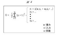
図3に示されるように、ニューラルネットワークは、入力層、中間層および出力層によって構成され、シナプスの結合強度は、各層の間に存在する「重みw」として表現される。 As shown in FIG. 3, the neural network is composed of an input layer, an intermediate layer and an output layer, and the synaptic connection strength is expressed as a "weight w" existing between each layer.
図3の画像を観察するために、入力層のサイズを画素数に対応させ、「入力x」を電気信号に対応させることができる。また、「入力x」および「重みw」から「出力y」を導くための計算は、図4に示される数式で表せることが知られている。 In order to observe the image of FIG. 3, the size of the input layer can be made to correspond to the number of pixels, and the "input x" can be made to correspond to the electric signal. Further, it is known that the calculation for deriving the "output y" from the "input x" and the "weight w" can be expressed by the mathematical formula shown in FIG.
画像から入力層にデータとして「入力x」が入ってくると、出力層には「出力y」として、「入力x」および「重みw」の積が算出される。所定の「出力y」は、「入力x」および「重みw」の種類が多い程に、それらの積が加算され、より詳細な情報となる。 When "input x" is input to the input layer from the image as data, the product of "input x" and "weight w" is calculated as "output y" in the output layer. As for the predetermined "output y", the more types of "input x" and "weight w" are, the more the product is added to the predetermined "output y", and the more detailed information is obtained.
また、中間層では、前段の積(例えば、入力層からの「入力x」および「重みw」の積)に対して、更に「重みw」が掛けられ、重み付けが成される。中間層が多い程、その度に重み付けが成されるので、「出力y」は、更に詳細な情報となる。 Further, in the intermediate layer, the product in the previous stage (for example, the product of the "input x" and the "weight w" from the input layer) is further multiplied by the "weight w" to be weighted. As the number of intermediate layers increases, weighting is performed each time, so that the "output y" becomes more detailed information.
例えば画像が猿である場合、「出力y1」は哺乳類に関する情報に関し、「出力y2」は顔の形状に関する情報に関し、「出力y3」は手の形状に関する情報に関するなど、それぞれの情報を関連付けて、正解に近づけることができる。 For example, when the image is a monkey, "output y1" is related to information about mammals, "output y2" is related to information about face shape, "output y3" is related to information about hand shape, and so on. You can get closer to the correct answer.
また、画像の正解は予め「正解t」としてデータ化されている。「出力y」と「正解t」との差分を用いて「誤差C」を求めることができ、「誤差C」の値が小さい程、正確な画像のデータを得ることができると言える。従って、「入力x」および「重みw」の各々の種類が多く、「出力y」の種類が多い程に、より正確な画像のデータを得ることができる。 Further, the correct answer of the image is preliminarily converted into data as "correct answer t". It can be said that the "error C" can be obtained by using the difference between the "output y" and the "correct answer t", and the smaller the value of the "error C", the more accurate image data can be obtained. Therefore, the more types of "input x" and "weight w" are, and the more types of "output y" are, the more accurate image data can be obtained.
例えば、以下に説明するニューラルネットワーク回路C1を用いる場合、「入力x」を制御ゲート電極CGの信号に対応させ、「重みw」を不揮発性メモリセルMCの閾値電圧Vthに対応させ、「出力y」を不揮発性メモリセルMCを流れる電流の値(ドレイン領域とソース領域との間を流れる電流の値)に対応させることができる。 For example, when the neural network circuit C1 described below is used, the "input x" corresponds to the signal of the control gate electrode CG, the "weight w" corresponds to the threshold voltage Vth of the non-volatile memory cell MC, and the "output y". Can correspond to the value of the current flowing through the non-volatile memory cell MC (the value of the current flowing between the drain region and the source region).
<半導体チップCHPおよびニューラルネットワーク回路C1の構成>
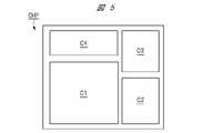
図5は、実施の形態1における半導体装置である半導体チップCHPのレイアウトを示す平面図である。半導体チップCHPは、例えば、ニューラルネットワーク回路C1、ROM(Read Only Memory)回路C2、RAM(Random Access Memory)回路C3、ロジック回路C4を有する。ここでは図示はしないが、半導体チップCHPには、更に入出力回路(I/O回路)およびアナログ回路などが設けられていてもよい。<Structure of semiconductor chip CHP and neural network circuit C1>
FIG. 5 is a plan view showing the layout of the semiconductor chip CHP, which is the semiconductor device according to the first embodiment. The semiconductor chip CHP includes, for example, a neural network circuit C1, a ROM (Read Only Memory) circuit C2, a RAM (Random Access Memory) circuit C3, and a logic circuit C4. Although not shown here, the semiconductor chip CHP may be further provided with an input / output circuit (I / O circuit), an analog circuit, and the like.
ニューラルネットワーク回路C1は、記憶情報を電気的に書き換え可能であり、半導体素子として、EEPROMが形成されている領域である。 The neural network circuit C1 is an area in which the stored information can be electrically rewritten and an EEPROM is formed as a semiconductor element.
ROM回路C2は、記憶情報の書込みを行わず、記憶情報の読出しのみを行う回路である。ROM回路C2では、半導体素子として、ニューラルネットワーク回路C1とほぼ同じ構造のEEPROMが適用できる。 The ROM circuit C2 is a circuit that does not write the stored information but only reads the stored information. In the ROM circuit C2, an EEPROM having almost the same structure as the neural network circuit C1 can be applied as a semiconductor element.
ロジック回路C3には、半導体素子として、1.5V程度の低電圧で駆動し、耐圧が低く、且つ、動作が速い低耐圧トランジスタが形成されている領域である。ロジック回路C3の半導体素子によって、例えばCPU(Central Processing Unit)が構成される。 The logic circuit C3 is a region in which a low withstand voltage transistor that is driven by a low voltage of about 1.5 V, has a low withstand voltage, and operates quickly is formed as a semiconductor element. For example, a CPU (Central Processing Unit) is configured by the semiconductor element of the logic circuit C3.
RAM回路C4は、例えばSRAM(Static RAM)であり、半導体素子として、ロジック回路C3とほぼ同様の構造の低耐圧トランジスタが形成されている領域である。 The RAM circuit C4 is, for example, an SRAM (Static RAM), and is a region in which a low withstand voltage transistor having a structure substantially similar to that of the logic circuit C3 is formed as a semiconductor element.
図6は、図5に示されるニューラルネットワーク回路C1のレイアウトを示す平面図である。 FIG. 6 is a plan view showing the layout of the neural network circuit C1 shown in FIG.
ニューラルネットワーク回路C1は、例えば、メモリセルアレイMCA、ワード線ドライバC5、入出力部C6、ビット線セレクタC7および演算回路C8を有する。 The neural network circuit C1 includes, for example, a memory cell array MCA, a word line driver C5, an input / output unit C6, a bit line selector C7, and an arithmetic circuit C8.
ワード線ドライバC5は、入出力部C6を介してニューラルネットワーク回路の外部から供給された電圧を、ワード線ドライバC5へ供給する。 The word line driver C5 supplies a voltage supplied from the outside of the neural network circuit to the word line driver C5 via the input / output unit C6.
ワード線ドライバC5には、昇圧回路などが設けられ、昇圧回路によって、書込み動作、消去動作または読出し動作において必要とされる電圧が生成される。各動作において、生成された各電圧のうち適切な電圧が、複数の制御ゲート電極CG、複数のメモリゲート電極MGおよび複数のソース線SLへ供給される。 The word line driver C5 is provided with a booster circuit or the like, and the booster circuit generates a voltage required for a write operation, an erase operation, or a read operation. In each operation, an appropriate voltage among the generated voltages is supplied to the plurality of control gate electrodes CG, the plurality of memory gate electrodes MG, and the plurality of source lines SL.
ビット線セレクタC7は、センスアンプを含み、選択された不揮発性メモリセルMCの記憶情報をビット線BLを介して読み出すことができる。また、ビット線セレクタC7は、ビット線BLを介して、記憶情報の書込みまたは消去の対象となる不揮発性メモリセルMCを選択できる。演算回路C8は、記憶情報の演算を行うことができる。 The bit line selector C7 includes a sense amplifier and can read the stored information of the selected non-volatile memory cell MC via the bit line BL. Further, the bit line selector C7 can select the non-volatile memory cell MC to be written or erased of the stored information via the bit line BL. The calculation circuit C8 can calculate the stored information.
<メモリセルアレイMCA(複数の不揮発性メモリセルMC)の構成>
図7は、実施の形態1におけるメモリセルアレイMCAを示す平面図である。図8は、図7に示されるA-A線に沿った不揮発性メモリセルMCの断面図である。<Configuration of memory cell array MCA (multiple non-volatile memory cell MC)>
FIG. 7 is a plan view showing the memory cell array MCA according to the first embodiment. FIG. 8 is a cross-sectional view of the non-volatile memory cell MC along the line AA shown in FIG.
実施の形態1における不揮発性メモリセルMCは、EEPROMであり、MONOS型のメモリセルである。複数の不揮発性メモリセルMCがアレイ状に配置されることで、メモリセルアレイMCAが構成されている。 The non-volatile memory cell MC in the first embodiment is an EEPROM and is a MONOS type memory cell. A memory cell array MCA is configured by arranging a plurality of non-volatile memory cell MCs in an array.
図8に示されるように、複数の不揮発性メモリセルMCは、それぞれ、ゲート絶縁膜GI1と、電荷蓄積層を有するゲート絶縁膜GI2と、制御ゲート電極CGと、メモリゲート電極MGと、ドレイン領域であるエクステンション領域EXDおよび拡散領域MDと、ソース領域であるエクステンション領域EXSおよび拡散領域MSとを有する。 As shown in FIG. 8, the plurality of non-volatile memory cells MC have a gate insulating film GI1, a gate insulating film GI2 having a charge storage layer, a control gate electrode CG, a memory gate electrode MG, and a drain region, respectively. It has an extension region EXD and a diffusion region MD which are source regions, and an extension region EXS and a diffusion region MS which are source regions.
なお、実施の形態1では、ゲート絶縁膜GI1および制御ゲート電極CGを有するトランジスタを選択トランジスタと呼称し、ゲート絶縁膜GI2およびメモリゲート電極MGを有するトランジスタをメモリトランジスタと呼称する場合がある。 In the first embodiment, the transistor having the gate insulating film GI1 and the control gate electrode CG may be referred to as a selection transistor, and the transistor having the gate insulating film GI2 and the memory gate electrode MG may be referred to as a memory transistor.
半導体基板SUBは、例えばp型のシリコンからなる。半導体基板SUBには、p型のウェル領域PWが形成されている。 The semiconductor substrate SUB is made of, for example, p-type silicon. A p-type well region PW is formed on the semiconductor substrate SUB.
半導体基板SUB上には、例えば酸化シリコンからなるゲート絶縁膜GI1が形成されている。ゲート絶縁膜GI1上には、例えば多結晶シリコンからなる制御ゲート電極CGが形成されている。 A gate insulating film GI1 made of, for example, silicon oxide is formed on the semiconductor substrate SUB. A control gate electrode CG made of, for example, polycrystalline silicon is formed on the gate insulating film GI1.
また、半導体基板SUB上および制御ゲート電極CGの側面上には、ゲート絶縁膜GI2が形成されている。ゲート絶縁膜GI1上には、例えば多結晶シリコンからなり、且つ、サイドウォール状に加工されたメモリゲート電極MGが形成されている。制御ゲート電極CGおよびメモリゲート電極MGは、X方向においてゲート絶縁膜GI2を介して互いに隣接している。 Further, a gate insulating film GI2 is formed on the semiconductor substrate SUB and on the side surface of the control gate electrode CG. A memory gate electrode MG made of, for example, polycrystalline silicon and processed into a sidewall is formed on the gate insulating film GI1. The control gate electrode CG and the memory gate electrode MG are adjacent to each other via the gate insulating film GI2 in the X direction.
ゲート絶縁膜GI2は、例えば積層膜からなり、上記積層膜は、酸化シリコン膜、電荷蓄積層および酸化シリコン膜からなる。上記電荷蓄積層は、メモリセルMCのデータを蓄積するために設けられた膜であり、電荷の保持が可能なトラップ準位を備える絶縁膜であり、例えば窒化シリコンからなる。 The gate insulating film GI2 is made of, for example, a laminated film, and the laminated film is made of a silicon oxide film, a charge storage layer, and a silicon oxide film. The charge storage layer is a film provided for storing data of the memory cell MC, is an insulating film having a trap level capable of retaining charges, and is made of, for example, silicon nitride.
制御ゲート電極CGおよびメモリゲート電極MGの各々の側面上には、例えば窒化シリコン膜のような絶縁膜からなるサイドウォールスペーサSWが形成されている。そして、制御ゲート電極CG側の半導体基板SUBには、n型のエクステンション領域EXDおよびn型の拡散領域MDが形成され、メモリゲート電極MG側の半導体基板SUBには、n型のエクステンション領域EXSおよびn型の拡散領域MSが形成されている。拡散領域MDおよび拡散領域MSの各々は、エクステンション領域EXDおよびエクステンション領域EXSの各々よりも高い不純物濃度を有する。 A sidewall spacer SW made of an insulating film such as a silicon nitride film is formed on each side surface of the control gate electrode CG and the memory gate electrode MG. The n-type extension region EXD and the n-type diffusion region MD are formed on the semiconductor substrate SUB on the control gate electrode CG side, and the n-type extension region EXS and the n-type extension region EXS are formed on the semiconductor substrate SUB on the memory gate electrode MG side. An n-type diffusion region MS is formed. Each of the diffusion region MD and the diffusion region MS has a higher impurity concentration than each of the extension region EXD and the extension region EXS.
このような不揮発性メモリセルMCを覆うように、半導体基板SUB上には、例えば酸化シリコンからなる層間絶縁膜IL0が形成されている。層間絶縁膜IL0には、複数のコンタクトホールが形成され、上記コンタクトホールの内部に、例えばタングステンを主体とする導電性膜が埋め込まれることで、層間絶縁膜IL0中に複数のプラグが形成されている。このような複数のプラグのうち、プラグPGDは拡散領域MDに電気的に接続され、プラグPGSは拡散領域MSに電気的に接続されている。 An interlayer insulating film IL0 made of, for example, silicon oxide is formed on the semiconductor substrate SUB so as to cover such a non-volatile memory cell MC. A plurality of contact holes are formed in the interlayer insulating film IL0, and by embedding a conductive film mainly composed of tungsten, for example, in the contact holes, a plurality of plugs are formed in the interlayer insulating film IL0. There is. Of such a plurality of plugs, the plug PGD is electrically connected to the diffusion region MD, and the plug PGS is electrically connected to the diffusion region MS.
図7に示されるように、拡散領域MDは、プラグPGDを介してビット線BLに電気的に接続され、拡散領域MSは、プラグPGSを介してソース線SLに電気的に接続されている。ビット線BLは、例えば1層目の配線であり、ソース線SLは、例えば2層目の配線である。各配線は、アルミニウム膜または銅膜を主体とした導電性膜からなる。 As shown in FIG. 7, the diffusion region MD is electrically connected to the bit line BL via the plug PGD, and the diffusion region MS is electrically connected to the source line SL via the plug PGS. The bit line BL is, for example, the wiring of the first layer, and the source line SL is, for example, the wiring of the second layer. Each wiring is made of a conductive film mainly composed of an aluminum film or a copper film.
メモリセルアレイMCAには複数の不揮発性メモリセルMCが含まれているが、複数の制御ゲート電極CGおよび複数のメモリゲート電極MGは、それぞれ、Y方向に延在している。そして、図1の従来技術では、ソース線SLがY方向に延在し、ビット線BLがX方向に延在していたが、図7の実施の形態1では、ソース線SLがX方向に延在し、ビット線BLがY方向に延在している。 Although the memory cell array MCA includes a plurality of non-volatile memory cells MC, the plurality of control gate electrodes CG and the plurality of memory gate electrodes MG each extend in the Y direction. Then, in the prior art of FIG. 1, the source line SL extends in the Y direction and the bit line BL extends in the X direction, but in the first embodiment of FIG. 7, the source line SL extends in the X direction. It extends, and the bit line BL extends in the Y direction.
このため、実施の形態1では、書込み動作および消去動作を、ビット単位で行うことができる。複数の不揮発性メモリセルMC(複数のメモリトランジスタ)の閾値電圧Vthは、それぞれ、電荷蓄積層に蓄積された電荷量によって変更できる。従って、複数の不揮発性メモリセルMCの閾値電圧Vthを変更させるための書込み動作および消去動作が、複数の不揮発性メモリセルMCに対して個別に行われる。 Therefore, in the first embodiment, the write operation and the erase operation can be performed in bit units. The threshold voltage Vth of the plurality of non-volatile memory cells MC (plurality of memory transistors) can be changed by the amount of charge stored in the charge storage layer, respectively. Therefore, the write operation and the erase operation for changing the threshold voltage Vth of the plurality of non-volatile memory cells MC are individually performed for the plurality of non-volatile memory cells MC.
<不揮発性メモリMCの各動作>
不揮発性メモリセルMCに対する書込み動作、消去動作および読出し動作の各電圧値は、図2に示されるものとほぼ同じであるが、後述の図9に示されるように、書込み動作および消去動作における電圧Vmgおよび電圧Vsが図2と異なっている。<Each operation of non-volatile memory MC>
The voltage values of the write operation, the erase operation, and the read operation for the non-volatile memory cell MC are almost the same as those shown in FIG. 2, but as shown in FIG. 9 described later, the voltage in the write operation and the erase operation. Vmg and voltage Vs are different from FIG.
また、図2および図9に示される各電圧は、メモリゲート電極MGに印加する電圧Vmg、ソース領域である拡散領域MSに印加する電圧Vs、制御ゲート電極CGに印加する電圧Vcg、および、ドレイン領域である拡散領域MDに印加する電圧Vdである。 Further, each voltage shown in FIGS. 2 and 9 includes a voltage Vmg applied to the memory gate electrode MG, a voltage Vs applied to the diffusion region MS which is the source region, a voltage Vcg applied to the control gate electrode CG, and a drain. It is a voltage Vd applied to the diffusion region MD which is a region.
なお、電圧値は一例であり、これらに限定されるものではなく、必要に応じて種々変更可能である。また、実施の形態1では、ゲート絶縁膜GF2中の電荷蓄積層への電子の注入が「書込み」であり、ゲート絶縁膜GF2中の電荷蓄積層へのホール(正孔)の注入が「消去」であると定義される。 The voltage value is an example, and is not limited to these, and can be variously changed as needed. Further, in the first embodiment, the injection of electrons into the charge storage layer in the gate insulating film GF2 is “writing”, and the injection of holes (holes) into the charge storage layer in the gate insulating film GF2 is “erasing”. Is defined as.
書込み動作は、SSI(Source Side Injection:ソースサイド注入)方式と呼ばれる、ホットエレクトロン注入で書込みを行う書込み方式を用いることができる。すなわち、ドレイン領域(拡散領域MD、エクステンション領域EXD)からソース領域(拡散領域MS、エクステンション領域EXS)へ向かって電子を加速させ、加速された電子を電荷蓄積層CSLへ注入することで、書込み動作が行われる。注入された電子は、電荷蓄積層中のトラップ準位に捕獲され、その結果、不揮発性メモリセルMC(メモリトランジスタ)の閾値電圧Vthが上昇する。すなわち、不揮発性メモリセルMCは、書込み状態となる。 As the writing operation, a writing method for writing by hot electron injection, which is called an SSI (Source Side Injection) method, can be used. That is, the writing operation is performed by accelerating the electrons from the drain region (diffusion region MD, extension region EXD) toward the source region (diffusion region MS, extension region EXS) and injecting the accelerated electrons into the charge storage layer CSL. Is done. The injected electrons are trapped in the trap level in the charge storage layer, and as a result, the threshold voltage Vth of the non-volatile memory cell MC (memory transistor) rises. That is, the non-volatile memory cell MC is in the write state.
消去動作は、BTBT(Band-To-Band Tunneling:バンド間トンネル現象)方式と呼ばれる、ホットホール注入により消去を行う消去方式を用いることができる。すなわち、ソース領域において、BTBT現象によりホールを発生させ、電界加速することで電荷蓄積層にホールを注入する。これにより、不揮発性メモリセルMC(メモリトランジスタ)の閾値電圧Vthが低下する。すなわち、不揮発性メモリセルMCは、消去状態となる。 As the erasing operation, an erasing method called a BTBT (Band-To-Band Tunneling) method, in which erasing is performed by hot hole injection, can be used. That is, in the source region, holes are generated by the BTBT phenomenon, and the holes are injected into the charge storage layer by accelerating the electric field. As a result, the threshold voltage Vth of the non-volatile memory cell MC (memory transistor) decreases. That is, the non-volatile memory cell MC is in the erased state.
読出し動作では、電圧Vmgが、書込み状態におけるメモリトランジスタの閾値電圧Vthと、消去状態におけるメモリトランジスタの閾値電圧との間の値に設定される。従って、ドレイン領域とソース領域との間に流れる電流の値を読み取ることで、不揮発性メモリセルMCが書込み状態であるか消去状態であるかを判別できる。 In the read operation, the voltage Vmg is set to a value between the threshold voltage Vth of the memory transistor in the write state and the threshold voltage of the memory transistor in the erase state. Therefore, by reading the value of the current flowing between the drain region and the source region, it is possible to determine whether the non-volatile memory cell MC is in the write state or the erase state.
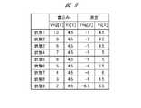
上述のように、実施の形態1では、書込み動作および消去動作における電圧Vmgおよび電圧Vsに、図9に示される値が用いられる。このような値を用いることで、書込み動作および消去動作において、メモリゲート電極MGとソース領域との間の電圧差を異ならせることができる。そうすると、図9に示されるように、各々の閾値電圧Vthが異なる複数の不揮発性メモリセルMCを用意できる。ここでは、各々の閾値電圧Vthが異なる9つの複数の不揮発性メモリセルMCが、状態1~9として示されている。 As described above, in the first embodiment, the values shown in FIG. 9 are used for the voltage Vmg and the voltage Vs in the write operation and the erase operation. By using such a value, the voltage difference between the memory gate electrode MG and the source region can be made different in the write operation and the erase operation. Then, as shown in FIG. 9, a plurality of non-volatile memory cells MC having different threshold voltages Vth can be prepared. Here, nine non-volatile memory cell MCs, each having a different threshold voltage Vth, are shown as states 1-9.
図10は、書込み後の不揮発性メモリセルMCの電流値の変化を示すグラフであり、図11は、消去後の不揮発性メモリセルMCの電流値の変化を示すグラフである。 FIG. 10 is a graph showing the change in the current value of the non-volatile memory cell MC after writing, and FIG. 11 is a graph showing the change in the current value of the non-volatile memory cell MC after erasing.
状態1~9のように、複数の不揮発性メモリセルMCの各々の閾値電圧Vthが異なっているので、複数の不揮発性メモリセルMCの読出し動作において、ドレイン領域とソース領域との間に流れる電流の値が、複数の不揮発性メモリセルMC毎に、それぞれ異なる。すなわち、複数の不揮発性メモリセルMCの閾値電圧Vthが、多段に設定され、複数の不揮発性メモリセルMCの各々に流れる電流の値も、多段に設定されている。 Since the threshold voltage Vth of each of the plurality of non-volatile memory cells MC is different as in the
<実施の形態1の主な効果>
実施の形態1によれば、図3および図4で説明した「入力x」、「重みw」および「出力y」を、ぞれぞれ、制御ゲート電極CGの信号、不揮発性メモリセルMCの閾値電圧Vth、および、不揮発性メモリセルMCを流れる電流の値(ドレイン領域とソース領域との間を流れる電流の値)に対応させることができる。<Main effects of
According to the first embodiment, the "input x", the "weight w" and the "output y" described in FIGS. 3 and 4 are set to the control gate electrode CG signal and the non-volatile memory cell MC, respectively. It can correspond to the threshold voltage Vth and the value of the current flowing through the non-volatile memory cell MC (the value of the current flowing between the drain region and the source region).
まず、複数の不揮発性メモリセルMCでは、ソース線SLおよびビット線BLの各々の延在方向を、従来技術と異なるように設計したことで、ビット単位での書込み動作および消去動作が可能となっている。 First, in the plurality of non-volatile memory cells MC, by designing the extending directions of the source line SL and the bit line BL to be different from those in the prior art, it is possible to perform write operation and erase operation in bit units. ing.
このため、図9の状態1~9のように、書込み動作および消去動作において、メモリゲート電極MGとソース領域との間の電圧差を異ならせることができ、各々の閾値電圧Vthが異なる複数の不揮発性メモリセルMCを用意することができる。 Therefore, as shown in the
これにより、図10および図11に示されるように、複数の不揮発性メモリセルMCの読出し動作において、ドレイン領域とソース領域との間に流れる電流の値を、複数の不揮発性メモリセルMC毎に、それぞれ異ならせることができる。そして、それぞれ異なる電流の値を用いて、ニューラルネットワーク回路C1のシナプスの結合強度を実現することができる。 As a result, as shown in FIGS. 10 and 11, in the read operation of the plurality of non-volatile memory cells MC, the value of the current flowing between the drain region and the source region is set for each of the plurality of non-volatile memory cells MC. , Can be different from each other. Then, the synaptic coupling strength of the neural network circuit C1 can be realized by using different current values.
このように、実施の形態1における複数の不揮発性メモリセルMCを用いて、ニューラルネットワーク回路C1におけるシナプスを実現することができる。 As described above, the synapses in the neural network circuit C1 can be realized by using the plurality of non-volatile memory cells MC in the first embodiment.
また、実施の形態1では、不揮発性メモリセルMCとして、トラップ準位を備える絶縁膜を電荷蓄積層とするMONOS型のメモリセルが適用されていた。MONOS型のメモリセルは、抵抗変化型メモリ(ReRAM)、磁気抵抗メモリ(MRAM)または強誘電体メモリ(FeRAM)などの他のメモリセルと比較して、不良ビットが少なく、書き換え耐性を長く維持できる。従って、実施の形態1における半導体装置は、長期に渡って信頼性を確保できる。 Further, in the first embodiment, as the non-volatile memory cell MC, a MONOS type memory cell having an insulating film having a trap level as a charge storage layer was applied. MONOS type memory cells have fewer defective bits and maintain longer rewrite resistance than other memory cells such as resistance change memory (ReRAM), magnetoresistive memory (MRAM) or ferroelectric memory (FeRAM). can. Therefore, the semiconductor device according to the first embodiment can ensure reliability for a long period of time.
また、図10および図11に示されるように、MONOS型の不揮発性メモリセルMCでは、安定した電流の推移を得られるので、「重みw」を安定して付与し易い。従って、他のメモリセルと比較して、ニューラルネットワーク回路C1の実現が容易である。 Further, as shown in FIGS. 10 and 11, in the MONOS type non-volatile memory cell MC, since a stable current transition can be obtained, it is easy to stably apply the “weight w”. Therefore, it is easier to realize the neural network circuit C1 as compared with other memory cells.
以上、本発明を上記実施の形態に基づいて具体的に説明したが、本発明は、上記実施の形態に限定されるものではなく、その要旨を逸脱しない範囲で種々変更可能である。 Although the present invention has been specifically described above based on the above-described embodiment, the present invention is not limited to the above-described embodiment and can be variously modified without departing from the gist thereof.
BL ビット線
C1 ニューラルネットワーク回路
C2 ROM回路
C3 RAM回路
C4 ロジック回路
C5 ワード線ドライバ
C6 入出力部
C7 ビット線セレクタ
C8 演算回路
CG 制御ゲート電極
CHP 半導体チップ(半導体装置)
EXD エクステンション領域(ドレイン領域)
EXS エクステンション領域(ソース領域)
GI1、GI2 ゲート絶縁膜
IL0 層間絶縁膜
MC 不揮発性メモリセル
MCA メモリセルアレイ
MD 拡散領域(ドレイン領域)
MG メモリゲート電極
MS 拡散領域(ソース領域)
PGD プラグ
PGS プラグ
PW ウェル領域
SL ソース線
SUB 半導体基板
SW サイドウォールスペーサBL Bit line C1 Neural network circuit C2 ROM circuit C3 RAM circuit C4 Logic circuit C5 Word line driver C6 Input / output unit C7 Bit line selector C8 Arithmetic circuit CG Control gate electrode CHP Semiconductor chip (semiconductor device)
EXD extension area (drain area)
EXS extension area (source area)
GI1, GI2 Gate insulating film IL0 Interlayer insulating film MC Non-volatile memory cell MCA Memory cell array MD Diffusion region (drain region)
MG memory gate electrode MS diffusion region (source region)
PGD plug PGS plug PW well area SL source line SUB semiconductor board SW sidewall spacer
Claims (6)
Translated fromJapanese前記複数の不揮発性メモリセルは、それぞれ、
半導体基板上に形成された第1ゲート絶縁膜と、
前記半導体基板上に形成され、且つ、電荷蓄積層を有する第2ゲート絶縁膜と、
前記第1ゲート絶縁膜上に形成された第1ゲート電極と、
前記第2ゲート絶縁膜上に形成された第2ゲート電極と、
前記第1ゲート電極側の前記半導体基板に形成されたドレイン領域と、
前記第2ゲート電極側の前記半導体基板に形成されたソース領域と、
を有し、
前記複数の前記第1ゲート電極および前記複数の第2ゲート電極は、それぞれ、平面視における第1方向に延在し、且つ、平面視において前記第1方向と交差する第2方向で互いに隣接し、
前記複数の前記ドレイン領域は、それぞれ、前記第1方向に延在するビット線に電気的に接続され、
前記複数の前記ソース領域は、それぞれ、前記第2方向に延在するソース線に電気的に接続されている、半導体装置。A semiconductor device equipped with a plurality of non-volatile memory cells.
Each of the plurality of non-volatile memory cells
The first gate insulating film formed on the semiconductor substrate and
A second gate insulating film formed on the semiconductor substrate and having a charge storage layer,
The first gate electrode formed on the first gate insulating film and
The second gate electrode formed on the second gate insulating film and
The drain region formed on the semiconductor substrate on the first gate electrode side and
The source region formed on the semiconductor substrate on the second gate electrode side and
Have,
The plurality of the first gate electrodes and the plurality of second gate electrodes each extend in the first direction in the plan view and are adjacent to each other in the second direction intersecting the first direction in the plan view. ,
The plurality of drain regions are each electrically connected to the bit wire extending in the first direction.
A semiconductor device in which the plurality of source regions are each electrically connected to a source line extending in the second direction.
前記複数の不揮発性メモリセルの閾値電圧は、それぞれ、前記電荷蓄積層に蓄積された電荷量によって変更でき、
前記複数の不揮発性メモリセルの閾値電圧を変更させるための書込み動作および消去動作が、前記複数の不揮発性メモリセルに対して個別に行われる、半導体装置。In the semiconductor device according to claim 1,
The threshold voltage of the plurality of non-volatile memory cells can be changed by the amount of charge stored in the charge storage layer, respectively.
A semiconductor device in which a write operation and an erase operation for changing the threshold voltage of the plurality of non-volatile memory cells are individually performed for the plurality of non-volatile memory cells.
前記書込み動作および前記消去動作において、前記第2ゲート電極と前記ソース領域との間の電圧差を異ならせることで、前記複数の不揮発性メモリセルの閾値電圧が、それぞれ異なる値となる、半導体装置。In the semiconductor device according to claim 2,
A semiconductor device in which the threshold voltages of the plurality of non-volatile memory cells become different values by making the voltage difference between the second gate electrode and the source region different in the writing operation and the erasing operation. ..
前記複数の不揮発性メモリセルの読出し動作において、前記ドレイン領域と前記ソース領域との間に流れる電流の値が、前記複数の不揮発性メモリセル毎に、それぞれ異なる、半導体装置。In the semiconductor device according to claim 3,
A semiconductor device in which in the read operation of the plurality of non-volatile memory cells, the value of the current flowing between the drain region and the source region is different for each of the plurality of non-volatile memory cells.
前記複数の不揮発性メモリセルは、ニューラルネットワーク回路の一部を構成し、
それぞれ異なる前記電流の値によって、シナプスの結合強度が実現される、半導体装置。In the semiconductor device according to claim 4,
The plurality of non-volatile memory cells form a part of the neural network circuit, and the plurality of non-volatile memory cells form a part of the neural network circuit.
A semiconductor device in which synaptic coupling strength is realized by different current values.
前記電荷蓄積層は、窒化シリコンからなり、
前記書込み動作では、前記ドレイン領域から前記電荷蓄積層へ電子が注入され、
前記消去動作では、前記ソース領域から前記電荷蓄積層へ正孔が注入される、半導体装置。In the semiconductor device according to claim 5,
The charge storage layer is made of silicon nitride and is made of silicon nitride.
In the writing operation, electrons are injected from the drain region into the charge storage layer, and the electrons are injected.
In the erasing operation, a semiconductor device in which holes are injected from the source region into the charge storage layer.
Priority Applications (4)
| Application Number | Priority Date | Filing Date | Title |
|---|---|---|---|
| JP2020186941AJP2022076545A (en) | 2020-11-10 | 2020-11-10 | Semiconductor device |
| US17/502,798US20220149058A1 (en) | 2020-11-10 | 2021-10-15 | Semiconductor device |
| TW110139993ATW202234679A (en) | 2020-11-10 | 2021-10-28 | Semiconductor device |
| CN202111286786.4ACN114464626A (en) | 2020-11-10 | 2021-11-02 | Semiconductor device |
Applications Claiming Priority (1)
| Application Number | Priority Date | Filing Date | Title |
|---|---|---|---|
| JP2020186941AJP2022076545A (en) | 2020-11-10 | 2020-11-10 | Semiconductor device |
Publications (1)
| Publication Number | Publication Date |
|---|---|
| JP2022076545Atrue JP2022076545A (en) | 2022-05-20 |
Family
ID=81405139
Family Applications (1)
| Application Number | Title | Priority Date | Filing Date |
|---|---|---|---|
| JP2020186941APendingJP2022076545A (en) | 2020-11-10 | 2020-11-10 | Semiconductor device |
Country Status (4)
| Country | Link |
|---|---|
| US (1) | US20220149058A1 (en) |
| JP (1) | JP2022076545A (en) |
| CN (1) | CN114464626A (en) |
| TW (1) | TW202234679A (en) |
Citations (6)
| Publication number | Priority date | Publication date | Assignee | Title |
|---|---|---|---|---|
| JP2002367381A (en)* | 2001-06-05 | 2002-12-20 | Sony Corp | Non-volatile semiconductor memory and its write method |
| JP2003158207A (en)* | 2001-11-26 | 2003-05-30 | Sony Corp | Nonvolatile semiconductor memory device and method for operating the same |
| JP2009301691A (en)* | 2008-06-17 | 2009-12-24 | Renesas Technology Corp | Nonvolatile semiconductor memory device |
| US20180190361A1 (en)* | 2016-12-13 | 2018-07-05 | Cypress Semiconductor Corporation | Suppression of Program Disturb with Bit Line and Select Gate Voltage Regulation |
| JP2019517138A (en)* | 2016-05-17 | 2019-06-20 | シリコン ストーリッジ テクノロージー インコーポレイテッドSilicon Storage Technology, Inc. | Deep Learning Neural Network Classifier Using Nonvolatile Memory Array |
| JP2021504868A (en)* | 2017-11-29 | 2021-02-15 | シリコン ストーリッジ テクノロージー インコーポレイテッドSilicon Storage Technology, Inc. | Precise and efficient adjustment mechanisms and algorithms for analog neuromorphic memory in artificial neural networks |
Family Cites Families (8)
| Publication number | Priority date | Publication date | Assignee | Title |
|---|---|---|---|---|
| KR100437470B1 (en)* | 2001-01-31 | 2004-06-23 | 삼성전자주식회사 | Semiconductor device having a flash memory cell and fabrication method thereof |
| JP4647175B2 (en)* | 2002-04-18 | 2011-03-09 | ルネサスエレクトロニクス株式会社 | Semiconductor integrated circuit device |
| JP5007017B2 (en)* | 2004-06-30 | 2012-08-22 | ルネサスエレクトロニクス株式会社 | Manufacturing method of semiconductor device |
| JP4795660B2 (en)* | 2004-09-29 | 2011-10-19 | ルネサスエレクトロニクス株式会社 | Semiconductor device |
| JP2009224425A (en)* | 2008-03-14 | 2009-10-01 | Renesas Technology Corp | Manufacturing method of nonvolatile semiconductor storage device and nonvolatile semiconductor storage device |
| CN109584933B (en)* | 2012-08-29 | 2023-07-25 | 瑞萨电子株式会社 | Semiconductor device |
| US9601194B2 (en)* | 2014-02-28 | 2017-03-21 | Crossbar, Inc. | NAND array comprising parallel transistor and two-terminal switching device |
| EP3182415B1 (en)* | 2014-08-14 | 2022-10-05 | Renesas Electronics Corporation | Semiconductor device |
- 2020
- 2020-11-10JPJP2020186941Apatent/JP2022076545A/enactivePending
- 2021
- 2021-10-15USUS17/502,798patent/US20220149058A1/ennot_activeAbandoned
- 2021-10-28TWTW110139993Apatent/TW202234679A/enunknown
- 2021-11-02CNCN202111286786.4Apatent/CN114464626A/enactivePending
Patent Citations (6)
| Publication number | Priority date | Publication date | Assignee | Title |
|---|---|---|---|---|
| JP2002367381A (en)* | 2001-06-05 | 2002-12-20 | Sony Corp | Non-volatile semiconductor memory and its write method |
| JP2003158207A (en)* | 2001-11-26 | 2003-05-30 | Sony Corp | Nonvolatile semiconductor memory device and method for operating the same |
| JP2009301691A (en)* | 2008-06-17 | 2009-12-24 | Renesas Technology Corp | Nonvolatile semiconductor memory device |
| JP2019517138A (en)* | 2016-05-17 | 2019-06-20 | シリコン ストーリッジ テクノロージー インコーポレイテッドSilicon Storage Technology, Inc. | Deep Learning Neural Network Classifier Using Nonvolatile Memory Array |
| US20180190361A1 (en)* | 2016-12-13 | 2018-07-05 | Cypress Semiconductor Corporation | Suppression of Program Disturb with Bit Line and Select Gate Voltage Regulation |
| JP2021504868A (en)* | 2017-11-29 | 2021-02-15 | シリコン ストーリッジ テクノロージー インコーポレイテッドSilicon Storage Technology, Inc. | Precise and efficient adjustment mechanisms and algorithms for analog neuromorphic memory in artificial neural networks |
Also Published As
| Publication number | Publication date |
|---|---|
| CN114464626A (en) | 2022-05-10 |
| US20220149058A1 (en) | 2022-05-12 |
| TW202234679A (en) | 2022-09-01 |
Similar Documents
| Publication | Publication Date | Title |
|---|---|---|
| US10664746B2 (en) | Neural network system | |
| US10777566B2 (en) | 3D array arranged for memory and in-memory sum-of-products operations | |
| US8588001B2 (en) | Integrated circuit memory devices having vertically arranged strings of memory cells therein and methods of operating same | |
| TWI254310B (en) | Ferroelectric memory wherein bit line capacitance can be maximized | |
| JP4004809B2 (en) | Semiconductor device and operation method thereof | |
| US11282578B2 (en) | Semiconductor storage apparatus including a memory cell array | |
| US11227660B2 (en) | Memory device and operating method thereof | |
| US11626165B2 (en) | Memory device | |
| US11974440B2 (en) | Page buffer circuit and memory device including the same | |
| CN115881191A (en) | Active refresh of edge data word lines for semicircular drain side select gates | |
| JP7458960B2 (en) | semiconductor equipment | |
| US20230138604A1 (en) | Non-volatile memory device | |
| US11616063B2 (en) | Semiconductor device and semiconductor memory device with improved diffusion suppression | |
| US20240055055A1 (en) | Memory device including page buffer circuit | |
| US12230330B2 (en) | Nonvolatile memory device for increasing reliability of data detected through page buffer | |
| US20220149058A1 (en) | Semiconductor device | |
| US8391044B2 (en) | Semiconductor memory device | |
| KR100222811B1 (en) | Nonvolatile semiconductor device | |
| CN115915761A (en) | Secondary cross-coupling effects and countermeasures in memory devices with semicircular drain-side select gates | |
| US10910059B2 (en) | Nonvolatile semiconductor memory device | |
| US20240233804A1 (en) | Voltage supply circuit, memory device including the same, and operating method of memory device | |
| US7733694B2 (en) | Nonvolatile semiconductor memory having a floating gate electrode formed within a trench | |
| CN119517127A (en) | Memory device and programming method thereof |
Legal Events
| Date | Code | Title | Description |
|---|---|---|---|
| A621 | Written request for application examination | Free format text:JAPANESE INTERMEDIATE CODE: A621 Effective date:20230315 | |
| A977 | Report on retrieval | Free format text:JAPANESE INTERMEDIATE CODE: A971007 Effective date:20231227 | |
| A131 | Notification of reasons for refusal | Free format text:JAPANESE INTERMEDIATE CODE: A131 Effective date:20240123 | |
| A02 | Decision of refusal | Free format text:JAPANESE INTERMEDIATE CODE: A02 Effective date:20240709 |