JP2022062088A - Display device - Google Patents
Display deviceDownload PDFInfo
- Publication number
- JP2022062088A JP2022062088AJP2022007579AJP2022007579AJP2022062088AJP 2022062088 AJP2022062088 AJP 2022062088AJP 2022007579 AJP2022007579 AJP 2022007579AJP 2022007579 AJP2022007579 AJP 2022007579AJP 2022062088 AJP2022062088 AJP 2022062088A
- Authority
- JP
- Japan
- Prior art keywords
- layer
- oxide semiconductor
- semiconductor layer
- thin film
- wiring
- Prior art date
- Legal status (The legal status is an assumption and is not a legal conclusion. Google has not performed a legal analysis and makes no representation as to the accuracy of the status listed.)
- Withdrawn
Links
Images


Classifications
- H—ELECTRICITY
- H10—SEMICONDUCTOR DEVICES; ELECTRIC SOLID-STATE DEVICES NOT OTHERWISE PROVIDED FOR
- H10D—INORGANIC ELECTRIC SEMICONDUCTOR DEVICES
- H10D30/00—Field-effect transistors [FET]
- H10D30/60—Insulated-gate field-effect transistors [IGFET]
- H10D30/67—Thin-film transistors [TFT]
- H10D30/674—Thin-film transistors [TFT] characterised by the active materials
- H10D30/6755—Oxide semiconductors, e.g. zinc oxide, copper aluminium oxide or cadmium stannate
- H—ELECTRICITY
- H01—ELECTRIC ELEMENTS
- H01L—SEMICONDUCTOR DEVICES NOT COVERED BY CLASS H10
- H01L21/00—Processes or apparatus adapted for the manufacture or treatment of semiconductor or solid state devices or of parts thereof
- H01L21/02—Manufacture or treatment of semiconductor devices or of parts thereof
- H01L21/02104—Forming layers
- H01L21/02107—Forming insulating materials on a substrate
- H01L21/02225—Forming insulating materials on a substrate characterised by the process for the formation of the insulating layer
- H—ELECTRICITY
- H01—ELECTRIC ELEMENTS
- H01L—SEMICONDUCTOR DEVICES NOT COVERED BY CLASS H10
- H01L21/00—Processes or apparatus adapted for the manufacture or treatment of semiconductor or solid state devices or of parts thereof
- H01L21/02—Manufacture or treatment of semiconductor devices or of parts thereof
- H01L21/04—Manufacture or treatment of semiconductor devices or of parts thereof the devices having potential barriers, e.g. a PN junction, depletion layer or carrier concentration layer
- H01L21/34—Manufacture or treatment of semiconductor devices or of parts thereof the devices having potential barriers, e.g. a PN junction, depletion layer or carrier concentration layer the devices having semiconductor bodies not provided for in groups H01L21/18, H10D48/04 and H10D48/07, with or without impurities, e.g. doping materials
- H01L21/46—Treatment of semiconductor bodies using processes or apparatus not provided for in groups H01L21/428
- H01L21/461—Treatment of semiconductor bodies using processes or apparatus not provided for in groups H01L21/428 to change their surface-physical characteristics or shape, e.g. etching, polishing, cutting
- H01L21/465—Chemical or electrical treatment, e.g. electrolytic etching
- H—ELECTRICITY
- H01—ELECTRIC ELEMENTS
- H01L—SEMICONDUCTOR DEVICES NOT COVERED BY CLASS H10
- H01L21/00—Processes or apparatus adapted for the manufacture or treatment of semiconductor or solid state devices or of parts thereof
- H01L21/02—Manufacture or treatment of semiconductor devices or of parts thereof
- H01L21/04—Manufacture or treatment of semiconductor devices or of parts thereof the devices having potential barriers, e.g. a PN junction, depletion layer or carrier concentration layer
- H01L21/34—Manufacture or treatment of semiconductor devices or of parts thereof the devices having potential barriers, e.g. a PN junction, depletion layer or carrier concentration layer the devices having semiconductor bodies not provided for in groups H01L21/18, H10D48/04 and H10D48/07, with or without impurities, e.g. doping materials
- H01L21/46—Treatment of semiconductor bodies using processes or apparatus not provided for in groups H01L21/428
- H01L21/461—Treatment of semiconductor bodies using processes or apparatus not provided for in groups H01L21/428 to change their surface-physical characteristics or shape, e.g. etching, polishing, cutting
- H01L21/4763—Deposition of non-insulating, e.g. conductive -, resistive -, layers on insulating layers; After-treatment of these layers
- H—ELECTRICITY
- H01—ELECTRIC ELEMENTS
- H01L—SEMICONDUCTOR DEVICES NOT COVERED BY CLASS H10
- H01L21/00—Processes or apparatus adapted for the manufacture or treatment of semiconductor or solid state devices or of parts thereof
- H01L21/67—Apparatus specially adapted for handling semiconductor or electric solid state devices during manufacture or treatment thereof; Apparatus specially adapted for handling wafers during manufacture or treatment of semiconductor or electric solid state devices or components ; Apparatus not specifically provided for elsewhere
- H01L21/67005—Apparatus not specifically provided for elsewhere
- H01L21/67011—Apparatus for manufacture or treatment
- H01L21/67017—Apparatus for fluid treatment
- H01L21/67063—Apparatus for fluid treatment for etching
- H01L21/67069—Apparatus for fluid treatment for etching for drying etching
- H—ELECTRICITY
- H10—SEMICONDUCTOR DEVICES; ELECTRIC SOLID-STATE DEVICES NOT OTHERWISE PROVIDED FOR
- H10D—INORGANIC ELECTRIC SEMICONDUCTOR DEVICES
- H10D30/00—Field-effect transistors [FET]
- H10D30/60—Insulated-gate field-effect transistors [IGFET]
- H10D30/67—Thin-film transistors [TFT]
- H10D30/6757—Thin-film transistors [TFT] characterised by the structure of the channel, e.g. transverse or longitudinal shape or doping profile
- H—ELECTRICITY
- H10—SEMICONDUCTOR DEVICES; ELECTRIC SOLID-STATE DEVICES NOT OTHERWISE PROVIDED FOR
- H10D—INORGANIC ELECTRIC SEMICONDUCTOR DEVICES
- H10D64/00—Electrodes of devices having potential barriers
- H10D64/20—Electrodes characterised by their shapes, relative sizes or dispositions
- H10D64/23—Electrodes carrying the current to be rectified, amplified, oscillated or switched, e.g. sources, drains, anodes or cathodes
- H10D64/251—Source or drain electrodes for field-effect devices
- H—ELECTRICITY
- H10—SEMICONDUCTOR DEVICES; ELECTRIC SOLID-STATE DEVICES NOT OTHERWISE PROVIDED FOR
- H10D—INORGANIC ELECTRIC SEMICONDUCTOR DEVICES
- H10D64/00—Electrodes of devices having potential barriers
- H10D64/20—Electrodes characterised by their shapes, relative sizes or dispositions
- H10D64/27—Electrodes not carrying the current to be rectified, amplified, oscillated or switched, e.g. gates
- H10D64/311—Gate electrodes for field-effect devices
- H10D64/411—Gate electrodes for field-effect devices for FETs
- H10D64/511—Gate electrodes for field-effect devices for FETs for IGFETs
- H—ELECTRICITY
- H10—SEMICONDUCTOR DEVICES; ELECTRIC SOLID-STATE DEVICES NOT OTHERWISE PROVIDED FOR
- H10D—INORGANIC ELECTRIC SEMICONDUCTOR DEVICES
- H10D86/00—Integrated devices formed in or on insulating or conducting substrates, e.g. formed in silicon-on-insulator [SOI] substrates or on stainless steel or glass substrates
- H10D86/01—Manufacture or treatment
- H10D86/021—Manufacture or treatment of multiple TFTs
- H10D86/0221—Manufacture or treatment of multiple TFTs comprising manufacture, treatment or patterning of TFT semiconductor bodies
- H—ELECTRICITY
- H10—SEMICONDUCTOR DEVICES; ELECTRIC SOLID-STATE DEVICES NOT OTHERWISE PROVIDED FOR
- H10D—INORGANIC ELECTRIC SEMICONDUCTOR DEVICES
- H10D86/00—Integrated devices formed in or on insulating or conducting substrates, e.g. formed in silicon-on-insulator [SOI] substrates or on stainless steel or glass substrates
- H10D86/40—Integrated devices formed in or on insulating or conducting substrates, e.g. formed in silicon-on-insulator [SOI] substrates or on stainless steel or glass substrates characterised by multiple TFTs
- H10D86/421—Integrated devices formed in or on insulating or conducting substrates, e.g. formed in silicon-on-insulator [SOI] substrates or on stainless steel or glass substrates characterised by multiple TFTs having a particular composition, shape or crystalline structure of the active layer
- H10D86/423—Integrated devices formed in or on insulating or conducting substrates, e.g. formed in silicon-on-insulator [SOI] substrates or on stainless steel or glass substrates characterised by multiple TFTs having a particular composition, shape or crystalline structure of the active layer comprising semiconductor materials not belonging to the Group IV, e.g. InGaZnO
- H—ELECTRICITY
- H10—SEMICONDUCTOR DEVICES; ELECTRIC SOLID-STATE DEVICES NOT OTHERWISE PROVIDED FOR
- H10D—INORGANIC ELECTRIC SEMICONDUCTOR DEVICES
- H10D86/00—Integrated devices formed in or on insulating or conducting substrates, e.g. formed in silicon-on-insulator [SOI] substrates or on stainless steel or glass substrates
- H10D86/40—Integrated devices formed in or on insulating or conducting substrates, e.g. formed in silicon-on-insulator [SOI] substrates or on stainless steel or glass substrates characterised by multiple TFTs
- H10D86/441—Interconnections, e.g. scanning lines
- H—ELECTRICITY
- H10—SEMICONDUCTOR DEVICES; ELECTRIC SOLID-STATE DEVICES NOT OTHERWISE PROVIDED FOR
- H10D—INORGANIC ELECTRIC SEMICONDUCTOR DEVICES
- H10D86/00—Integrated devices formed in or on insulating or conducting substrates, e.g. formed in silicon-on-insulator [SOI] substrates or on stainless steel or glass substrates
- H10D86/40—Integrated devices formed in or on insulating or conducting substrates, e.g. formed in silicon-on-insulator [SOI] substrates or on stainless steel or glass substrates characterised by multiple TFTs
- H10D86/60—Integrated devices formed in or on insulating or conducting substrates, e.g. formed in silicon-on-insulator [SOI] substrates or on stainless steel or glass substrates characterised by multiple TFTs wherein the TFTs are in active matrices
- H—ELECTRICITY
- H10—SEMICONDUCTOR DEVICES; ELECTRIC SOLID-STATE DEVICES NOT OTHERWISE PROVIDED FOR
- H10D—INORGANIC ELECTRIC SEMICONDUCTOR DEVICES
- H10D99/00—Subject matter not provided for in other groups of this subclass
- G—PHYSICS
- G02—OPTICS
- G02F—OPTICAL DEVICES OR ARRANGEMENTS FOR THE CONTROL OF LIGHT BY MODIFICATION OF THE OPTICAL PROPERTIES OF THE MEDIA OF THE ELEMENTS INVOLVED THEREIN; NON-LINEAR OPTICS; FREQUENCY-CHANGING OF LIGHT; OPTICAL LOGIC ELEMENTS; OPTICAL ANALOGUE/DIGITAL CONVERTERS
- G02F1/00—Devices or arrangements for the control of the intensity, colour, phase, polarisation or direction of light arriving from an independent light source, e.g. switching, gating or modulating; Non-linear optics
- G02F1/01—Devices or arrangements for the control of the intensity, colour, phase, polarisation or direction of light arriving from an independent light source, e.g. switching, gating or modulating; Non-linear optics for the control of the intensity, phase, polarisation or colour
- G02F1/13—Devices or arrangements for the control of the intensity, colour, phase, polarisation or direction of light arriving from an independent light source, e.g. switching, gating or modulating; Non-linear optics for the control of the intensity, phase, polarisation or colour based on liquid crystals, e.g. single liquid crystal display cells
- G02F1/133—Constructional arrangements; Operation of liquid crystal cells; Circuit arrangements
- G02F1/1333—Constructional arrangements; Manufacturing methods
- G02F1/1343—Electrodes
- G02F1/134309—Electrodes characterised by their geometrical arrangement
- G—PHYSICS
- G02—OPTICS
- G02F—OPTICAL DEVICES OR ARRANGEMENTS FOR THE CONTROL OF LIGHT BY MODIFICATION OF THE OPTICAL PROPERTIES OF THE MEDIA OF THE ELEMENTS INVOLVED THEREIN; NON-LINEAR OPTICS; FREQUENCY-CHANGING OF LIGHT; OPTICAL LOGIC ELEMENTS; OPTICAL ANALOGUE/DIGITAL CONVERTERS
- G02F1/00—Devices or arrangements for the control of the intensity, colour, phase, polarisation or direction of light arriving from an independent light source, e.g. switching, gating or modulating; Non-linear optics
- G02F1/01—Devices or arrangements for the control of the intensity, colour, phase, polarisation or direction of light arriving from an independent light source, e.g. switching, gating or modulating; Non-linear optics for the control of the intensity, phase, polarisation or colour
- G02F1/13—Devices or arrangements for the control of the intensity, colour, phase, polarisation or direction of light arriving from an independent light source, e.g. switching, gating or modulating; Non-linear optics for the control of the intensity, phase, polarisation or colour based on liquid crystals, e.g. single liquid crystal display cells
- G02F1/133—Constructional arrangements; Operation of liquid crystal cells; Circuit arrangements
- G02F1/136—Liquid crystal cells structurally associated with a semi-conducting layer or substrate, e.g. cells forming part of an integrated circuit
- G02F1/1362—Active matrix addressed cells
- G02F1/136227—Through-hole connection of the pixel electrode to the active element through an insulation layer
- G—PHYSICS
- G09—EDUCATION; CRYPTOGRAPHY; DISPLAY; ADVERTISING; SEALS
- G09G—ARRANGEMENTS OR CIRCUITS FOR CONTROL OF INDICATING DEVICES USING STATIC MEANS TO PRESENT VARIABLE INFORMATION
- G09G2300/00—Aspects of the constitution of display devices
- G09G2300/04—Structural and physical details of display devices
- G09G2300/0404—Matrix technologies
- G09G2300/0408—Integration of the drivers onto the display substrate
- G—PHYSICS
- G09—EDUCATION; CRYPTOGRAPHY; DISPLAY; ADVERTISING; SEALS
- G09G—ARRANGEMENTS OR CIRCUITS FOR CONTROL OF INDICATING DEVICES USING STATIC MEANS TO PRESENT VARIABLE INFORMATION
- G09G2300/00—Aspects of the constitution of display devices
- G09G2300/08—Active matrix structure, i.e. with use of active elements, inclusive of non-linear two terminal elements, in the pixels together with light emitting or modulating elements
- G09G2300/0809—Several active elements per pixel in active matrix panels
- G—PHYSICS
- G09—EDUCATION; CRYPTOGRAPHY; DISPLAY; ADVERTISING; SEALS
- G09G—ARRANGEMENTS OR CIRCUITS FOR CONTROL OF INDICATING DEVICES USING STATIC MEANS TO PRESENT VARIABLE INFORMATION
- G09G2310/00—Command of the display device
- G09G2310/02—Addressing, scanning or driving the display screen or processing steps related thereto
- G09G2310/0243—Details of the generation of driving signals
- G09G2310/0251—Precharge or discharge of pixel before applying new pixel voltage
- G—PHYSICS
- G09—EDUCATION; CRYPTOGRAPHY; DISPLAY; ADVERTISING; SEALS
- G09G—ARRANGEMENTS OR CIRCUITS FOR CONTROL OF INDICATING DEVICES USING STATIC MEANS TO PRESENT VARIABLE INFORMATION
- G09G2310/00—Command of the display device
- G09G2310/02—Addressing, scanning or driving the display screen or processing steps related thereto
- G09G2310/0264—Details of driving circuits
- G09G2310/0286—Details of a shift registers arranged for use in a driving circuit
- G—PHYSICS
- G09—EDUCATION; CRYPTOGRAPHY; DISPLAY; ADVERTISING; SEALS
- G09G—ARRANGEMENTS OR CIRCUITS FOR CONTROL OF INDICATING DEVICES USING STATIC MEANS TO PRESENT VARIABLE INFORMATION
- G09G2310/00—Command of the display device
- G09G2310/08—Details of timing specific for flat panels, other than clock recovery
- G—PHYSICS
- G09—EDUCATION; CRYPTOGRAPHY; DISPLAY; ADVERTISING; SEALS
- G09G—ARRANGEMENTS OR CIRCUITS FOR CONTROL OF INDICATING DEVICES USING STATIC MEANS TO PRESENT VARIABLE INFORMATION
- G09G3/00—Control arrangements or circuits, of interest only in connection with visual indicators other than cathode-ray tubes
- G09G3/20—Control arrangements or circuits, of interest only in connection with visual indicators other than cathode-ray tubes for presentation of an assembly of a number of characters, e.g. a page, by composing the assembly by combination of individual elements arranged in a matrix no fixed position being assigned to or needed to be assigned to the individual characters or partial characters
- G09G3/34—Control arrangements or circuits, of interest only in connection with visual indicators other than cathode-ray tubes for presentation of an assembly of a number of characters, e.g. a page, by composing the assembly by combination of individual elements arranged in a matrix no fixed position being assigned to or needed to be assigned to the individual characters or partial characters by control of light from an independent source
- G09G3/36—Control arrangements or circuits, of interest only in connection with visual indicators other than cathode-ray tubes for presentation of an assembly of a number of characters, e.g. a page, by composing the assembly by combination of individual elements arranged in a matrix no fixed position being assigned to or needed to be assigned to the individual characters or partial characters by control of light from an independent source using liquid crystals
- G09G3/3611—Control of matrices with row and column drivers
- G09G3/3648—Control of matrices with row and column drivers using an active matrix
- G—PHYSICS
- G09—EDUCATION; CRYPTOGRAPHY; DISPLAY; ADVERTISING; SEALS
- G09G—ARRANGEMENTS OR CIRCUITS FOR CONTROL OF INDICATING DEVICES USING STATIC MEANS TO PRESENT VARIABLE INFORMATION
- G09G3/00—Control arrangements or circuits, of interest only in connection with visual indicators other than cathode-ray tubes
- G09G3/20—Control arrangements or circuits, of interest only in connection with visual indicators other than cathode-ray tubes for presentation of an assembly of a number of characters, e.g. a page, by composing the assembly by combination of individual elements arranged in a matrix no fixed position being assigned to or needed to be assigned to the individual characters or partial characters
- G09G3/34—Control arrangements or circuits, of interest only in connection with visual indicators other than cathode-ray tubes for presentation of an assembly of a number of characters, e.g. a page, by composing the assembly by combination of individual elements arranged in a matrix no fixed position being assigned to or needed to be assigned to the individual characters or partial characters by control of light from an independent source
- G09G3/36—Control arrangements or circuits, of interest only in connection with visual indicators other than cathode-ray tubes for presentation of an assembly of a number of characters, e.g. a page, by composing the assembly by combination of individual elements arranged in a matrix no fixed position being assigned to or needed to be assigned to the individual characters or partial characters by control of light from an independent source using liquid crystals
- G09G3/3611—Control of matrices with row and column drivers
- G09G3/3674—Details of drivers for scan electrodes
- G09G3/3677—Details of drivers for scan electrodes suitable for active matrices only
- G—PHYSICS
- G11—INFORMATION STORAGE
- G11C—STATIC STORES
- G11C19/00—Digital stores in which the information is moved stepwise, e.g. shift registers
- G11C19/28—Digital stores in which the information is moved stepwise, e.g. shift registers using semiconductor elements
- H—ELECTRICITY
- H10—SEMICONDUCTOR DEVICES; ELECTRIC SOLID-STATE DEVICES NOT OTHERWISE PROVIDED FOR
- H10K—ORGANIC ELECTRIC SOLID-STATE DEVICES
- H10K59/00—Integrated devices, or assemblies of multiple devices, comprising at least one organic light-emitting element covered by group H10K50/00
- H10K59/10—OLED displays
- H10K59/12—Active-matrix OLED [AMOLED] displays
- H10K59/121—Active-matrix OLED [AMOLED] displays characterised by the geometry or disposition of pixel elements
- H10K59/1213—Active-matrix OLED [AMOLED] displays characterised by the geometry or disposition of pixel elements the pixel elements being TFTs
Landscapes
- Engineering & Computer Science (AREA)
- Microelectronics & Electronic Packaging (AREA)
- Condensed Matter Physics & Semiconductors (AREA)
- General Physics & Mathematics (AREA)
- Manufacturing & Machinery (AREA)
- Computer Hardware Design (AREA)
- Physics & Mathematics (AREA)
- Power Engineering (AREA)
- Thin Film Transistor (AREA)
- Liquid Crystal (AREA)
- Electroluminescent Light Sources (AREA)
- Devices For Indicating Variable Information By Combining Individual Elements (AREA)
- Drying Of Semiconductors (AREA)
- Electrodes Of Semiconductors (AREA)
- Weting (AREA)
Abstract
Translated fromJapaneseDescription
Translated fromJapanese酸化物半導体を用いた半導体装置の作製方法に関する。The present invention relates to a method for manufacturing a semiconductor device using an oxide semiconductor.
近年、酸化物半導体を用いて薄膜トランジスタ(TFTとも呼ぶ)を作製し、電子デバイ
ス等に応用する技術が注目されている。例えば、特許文献1や特許文献2には、酸化物半
導体膜として酸化亜鉛やIn-Ga-Zn-O系酸化物半導体などを用いて、画像表示装
置のスイッチング素子などを作製する技術が開示されている。In recent years, a technique for producing a thin film transistor (also called a TFT) using an oxide semiconductor and applying it to an electronic device or the like has attracted attention. For example,
酸化物半導体を加工する技術としてはエッチング処理が代表的であるが(特許文献3、特
許文献4等参照)、例えば、ウエットエッチングは等方的なエッチングであるため、素子
の微細化には不向きという問題がある。また、薬液を用いる処理であるため、制御性の点
で課題がある。一方で、ドライエッチングは、微細化、制御性の面では有利であるが、エ
ッチングレートが小さく、処理に時間がかかるという問題がある。また、使用する装置に
よっては、エッチングの面内ばらつきが生じる可能性が高い。Etching processing is a typical technique for processing oxide semiconductors (see Patent Documents 3 and 4), but for example, wet etching is isotropic etching and is not suitable for device miniaturization. There is a problem. In addition, since the treatment uses a chemical solution, there is a problem in terms of controllability. On the other hand, dry etching is advantageous in terms of miniaturization and controllability, but has a problem that the etching rate is small and processing takes time. Further, depending on the apparatus used, there is a high possibility that in-plane variation in etching will occur.
このように、酸化物半導体を加工する技術は既にいくつか存在していたが、酸化物半導体
を用いて半導体装置を作製しようとする場合に要求される条件を満たす加工技術は、未だ
確立されていなかった。As described above, although some techniques for processing oxide semiconductors have already existed, processing techniques that satisfy the conditions required when manufacturing semiconductor devices using oxide semiconductors have not yet been established. There wasn't.
また、酸化物半導体にはインジウムなどの希少金属が使用されているが、従来のエッチン
グをはじめとする加工技術においては、これらの高価な金属類を含有する酸化物半導体層
は、成膜された膜のうち大部分が除去されると共に廃棄されていた。このため、従来の加
工技術では酸化物半導体を適用する半導体装置の作製にかかるコストを低減することが困
難であった。また、省資源問題への対応が求められていた。In addition, rare metals such as indium are used for oxide semiconductors, but in conventional processing techniques such as etching, oxide semiconductor layers containing these expensive metals are formed into a film. Most of the membrane was removed and discarded. Therefore, it has been difficult to reduce the cost of manufacturing a semiconductor device to which an oxide semiconductor is applied by the conventional processing technique. In addition, it was required to deal with the resource saving problem.
上記問題点に鑑み、酸化物半導体を用いた半導体装置を作製する際の加工技術を確立する
ことを課題の一とする。または、省資源問題に対応した半導体装置の作製方法を提供する
ことを課題の一とする。In view of the above problems, one of the problems is to establish a processing technique for manufacturing a semiconductor device using an oxide semiconductor. Alternatively, one of the issues is to provide a method for manufacturing a semiconductor device corresponding to the resource saving problem.
開示する発明の一例は、活性層として機能する島状の酸化物半導体層と、それを覆う導電
層を、ドライエッチングにより加工する。例えば、塩素と酸素を含むガスを用いたドライ
エッチングにより、導電層を加工してソース電極及びドレイン電極を形成すると共に、酸
化物半導体層の一部を除去し、島状の酸化物半導体層に凹部を形成する。この際、島状の
酸化物半導体層の下方に存在するゲート絶縁層には、酸化シリコンを含む材料を用いるこ
とが好ましい。In one example of the disclosed invention, an island-shaped oxide semiconductor layer that functions as an active layer and a conductive layer that covers the island-shaped oxide semiconductor layer are processed by dry etching. For example, by dry etching using a gas containing chlorine and oxygen, the conductive layer is processed to form a source electrode and a drain electrode, and a part of the oxide semiconductor layer is removed to form an island-shaped oxide semiconductor layer. Form a recess. At this time, it is preferable to use a material containing silicon oxide for the gate insulating layer existing below the island-shaped oxide semiconductor layer.
又は、ゲート絶縁層上方の酸化物半導体層を、ウエットエッチングにより島状の酸化物半
導体層に加工する。Alternatively, the oxide semiconductor layer above the gate insulating layer is processed into an island-shaped oxide semiconductor layer by wet etching.
より詳細には、次の通りである。More details are as follows.
開示する発明の一例は、基板上に、ゲート電極と、該ゲート電極上方のゲート絶縁層と、
該ゲート絶縁層上方の酸化物半導体層と、を形成し、ウエットエッチングにより、酸化物
半導体層を加工して島状の酸化物半導体層を形成し、島状の酸化物半導体層を覆う導電層
を形成し、ドライエッチングにより、導電層を加工してソース電極及びドレイン電極を形
成し(形成すると共に)、島状の酸化物半導体層の一部を除去し、島状の酸化物半導体層
に凹部を形成することを特徴とする。An example of the disclosed invention is a gate electrode, a gate insulating layer above the gate electrode, and a gate insulating layer on the substrate.
An oxide semiconductor layer above the gate insulating layer is formed, and the oxide semiconductor layer is processed by wet etching to form an island-shaped oxide semiconductor layer, and a conductive layer covering the island-shaped oxide semiconductor layer. Is formed, and the conductive layer is processed by dry etching to form (form) a source electrode and a drain electrode, and a part of the island-shaped oxide semiconductor layer is removed to form an island-shaped oxide semiconductor layer. It is characterized by forming a recess.
開示する発明の他の一例は、基板上に、ゲート電極と、該ゲート電極上方のゲート絶縁層
と、該ゲート絶縁層上方の第1の酸化物半導体層と、を形成し、第1の酸化物半導体層上
方に、第1の酸化物半導体層より導電率が高い第2の酸化物半導体層を形成し、ウエット
エッチングにより、第1の酸化物半導体層及び第2の酸化物半導体層を加工して島状の第
1の酸化物半導体層及び島状の第2の酸化物半導体層を形成し、島状の第2の酸化物半導
体層を覆う導電層を形成し、ドライエッチングにより、導電層を加工してソース電極及び
ドレイン電極を形成し(形成すると共に)、島状の第1の酸化物半導体層及び島状の第2
の酸化物半導体層の一部を除去し、島状の第1の酸化物半導体層に凹部を形成することを
特徴とする。In another example of the disclosed invention, a gate electrode, a gate insulating layer above the gate electrode, and a first oxide semiconductor layer above the gate insulating layer are formed on a substrate, and a first oxidation is performed. A second oxide semiconductor layer having a higher conductivity than the first oxide semiconductor layer is formed above the physical semiconductor layer, and the first oxide semiconductor layer and the second oxide semiconductor layer are processed by wet etching. A first island-shaped oxide semiconductor layer and an island-shaped second oxide semiconductor layer are formed, and a conductive layer covering the island-shaped second oxide semiconductor layer is formed. The layers are processed to form (and together with) the source and drain electrodes, the island-shaped first oxide semiconductor layer and the island-shaped second.
It is characterized in that a part of the oxide semiconductor layer of the above is removed to form a recess in the island-shaped first oxide semiconductor layer.
上記において、酸化物半導体層(第1の酸化物半導体層、及び第2の酸化物半導体層を含
む)は、インジウム、ガリウム及び亜鉛を含んでいても良い。また、導電層として、酸化
物半導体層(第1の酸化物半導体層、及び第2の酸化物半導体層を含む)に用いる材料よ
りドライエッチングにおけるエッチングレートが大きい材料を用いることができる。In the above, the oxide semiconductor layer (including the first oxide semiconductor layer and the second oxide semiconductor layer) may contain indium, gallium and zinc. Further, as the conductive layer, a material having a higher etching rate in dry etching than the material used for the oxide semiconductor layer (including the first oxide semiconductor layer and the second oxide semiconductor layer) can be used.
また、上記ドライエッチングは、塩素を含むガスを用いて行うことができる。この場合、
ゲート絶縁層は、酸化シリコンを含む材料を用いて形成し、塩素を含むガスは酸素を含ん
でいることが好ましい。また、酸素の含有量を、塩素を含むガスの15体積%以上として
も良い。Further, the dry etching can be performed using a gas containing chlorine. in this case,
The gate insulating layer is preferably formed by using a material containing silicon oxide, and the gas containing chlorine preferably contains oxygen. Further, the oxygen content may be 15% by volume or more of the gas containing chlorine.
また、上記ウエットエッチングの廃液から、金属元素を回収することもできる。In addition, metal elements can be recovered from the waste liquid of the wet etching.
開示する発明の一例は、基板上に、ゲート電極と、該ゲート電極上方のゲート絶縁層と、
該ゲート絶縁層上方の島状の酸化物半導体層と、を形成し、島状の酸化物半導体層を覆う
導電層を形成し、塩素と酸素を含むガスを用いたドライエッチングにより、導電層を加工
してソース電極及びドレイン電極を形成し(形成すると共に)、酸化物半導体層の一部を
除去し、島状の酸化物半導体層に凹部を形成することを特徴とする。An example of the disclosed invention is a gate electrode, a gate insulating layer above the gate electrode, and a gate insulating layer on the substrate.
An island-shaped oxide semiconductor layer above the gate insulating layer is formed, a conductive layer covering the island-shaped oxide semiconductor layer is formed, and the conductive layer is formed by dry etching using a gas containing chlorine and oxygen. It is characterized in that a source electrode and a drain electrode are formed (as well as formed) by processing, a part of the oxide semiconductor layer is removed, and a recess is formed in the island-shaped oxide semiconductor layer.
上記において、酸化物半導体層は、インジウム、ガリウム及び亜鉛を含んでいても良い。
また、導電層として、酸化物半導体層に用いる材料よりドライエッチングにおけるエッチ
ングレートが大きい材料を用いることができる。また、ゲート絶縁層は、酸化シリコンを
含む材料を用いて形成すると良い。また、酸素の含有量を、塩素と酸素を含むガスの15
体積%以上としても良い。In the above, the oxide semiconductor layer may contain indium, gallium and zinc.
Further, as the conductive layer, a material having a higher etching rate in dry etching than the material used for the oxide semiconductor layer can be used. Further, the gate insulating layer may be formed by using a material containing silicon oxide. In addition, the oxygen content is 15 of the gas containing chlorine and oxygen.
The volume may be% or more.
なお、「エッチングレート」とは、単位時間あたりにエッチングされる量(被エッチング
量)を意味する。したがって、「エッチングレートが大きい」とは、よりエッチングされ
やすいことを意味し、「エッチングレートが小さい」とは、よりエッチングされにくいこ
とを意味する。また、「エッチング選択比がとれる」とは、例えば、A層とB層をエッチ
ングする場合に、A層のエッチングレートとB層のエッチングレートに十分な差を有する
ことにより、A層とB層の一方をより多くエッチングできることを意味する。The "etching rate" means an amount to be etched (amount to be etched) per unit time. Therefore, "high etching rate" means that it is easier to be etched, and "small etching rate" means that it is more difficult to be etched. Further, "the etching selectivity can be obtained" means that, for example, when the A layer and the B layer are etched, the etching rate of the A layer and the etching rate of the B layer have a sufficient difference, so that the A layer and the B layer are obtained. It means that one can be etched more.
なお、本明細書中で用いることができる酸化物半導体の一例としては、InMO3(Zn
O)m(m>0)で表記されるものがある。ここで、Mは、ガリウム(Ga)、鉄(Fe
)、ニッケル(Ni)、マンガン(Mn)及びコバルト(Co)から選ばれた一の金属元
素又は複数の金属元素を示す。例えばMとしてGaが選択される場合には、Gaのみの場
合の他に、GaとNiや、GaとFeなど、Ga以外の上記金属元素が選択される場合を
含む。また、上記酸化物半導体において、Mとして含まれる金属元素の他に、不純物元素
としてFe、Niその他の遷移金属元素、又は該遷移金属の酸化物が含まれているものが
ある。本明細書においては、上記酸化物半導体のうち、Mとして少なくともガリウムを含
むものをIn-Ga-Zn-O系酸化物半導体と呼び、当該材料を用いた薄膜をIn-G
a-Zn-O系非単結晶膜と呼ぶことがある。An example of an oxide semiconductor that can be used in the present specification is InMO3 (Zn).
O) Some are represented bym (m> 0). Here, M is gallium (Ga) and iron (Fe).
), Nickel (Ni), manganese (Mn) and cobalt (Co). For example, when Ga is selected as M, it includes the case where Ga and Ni, Ga and Fe, and the above metal elements other than Ga are selected, in addition to the case where only Ga is selected. Further, in the oxide semiconductor, in addition to the metal element contained as M, Fe, Ni and other transition metal elements, or an oxide of the transition metal is contained as an impurity element. In the present specification, among the oxide semiconductors, those containing at least gallium as M are referred to as In—Ga—Zn—O oxide semiconductors, and thin films using the material are referred to as In—G.
It may be called an a—Zn—O system non-single crystal film.
なお、本明細書中において半導体装置とは、半導体特性を利用することで機能しうる装置
全般を指し、表示装置、半導体回路および電子機器は全て半導体装置に含まれる。In the present specification, the semiconductor device refers to all devices that can function by utilizing the semiconductor characteristics, and the display device, the semiconductor circuit, and the electronic device are all included in the semiconductor device.
開示する発明において、活性層として機能する島状の酸化物半導体層と、それを覆う導電
層を、ドライエッチングにより加工することで、半導体装置の微細化が可能となり、半導
体装置の性能が向上する。又は、ゲート絶縁層上方の酸化物半導体層を、ウエットエッチ
ングにより島状の酸化物半導体層に加工することで、スループットを向上させることがで
きる。In the disclosed invention, by processing the island-shaped oxide semiconductor layer that functions as an active layer and the conductive layer that covers the island-shaped oxide semiconductor layer by dry etching, the semiconductor device can be miniaturized and the performance of the semiconductor device is improved. .. Alternatively, the throughput can be improved by processing the oxide semiconductor layer above the gate insulating layer into an island-shaped oxide semiconductor layer by wet etching.
または、比較的エッチングの制御性が要求されないゲート絶縁層上方の酸化物半導体層の
エッチング(島状酸化物半導体層への加工)をウエットエッチングにより行い、微細化や
エッチングの制御性が要求されるチャネルエッチをドライエッチングにより行うことによ
り、作製プロセス全体としてスループットを向上させると共に半導体装置を高性能化する
ことができる。Alternatively, etching of the oxide semiconductor layer above the gate insulating layer (processing into an island-shaped oxide semiconductor layer), which does not require relatively etching controllability, is performed by wet etching, and miniaturization and etching controllability are required. By performing channel etching by dry etching, it is possible to improve the throughput and improve the performance of the semiconductor device in the entire manufacturing process.
または、酸化物半導体層を島状に加工する際にウエットエッチングを用いて行い、当該エ
ッチング後の廃液から酸化物半導体層に含まれるインジウム等の材料を回収して再利用す
ることにより、資源を有効活用し低コスト化することができる。Alternatively, when the oxide semiconductor layer is processed into an island shape, wet etching is used to recover resources such as indium contained in the oxide semiconductor layer from the waste liquid after the etching and reuse the resources. It can be effectively used and the cost can be reduced.
実施の形態について、図面を用いて詳細に説明する。但し、本発明は以下に示す実施の形
態の記載内容に限定されず、発明の趣旨から逸脱することなく形態及び詳細を様々に変更
し得ることは当業者にとって自明である。また、異なる実施の形態に係る構成は、適宜組
み合わせて実施することができる。なお、以下に説明する発明の構成において、同一部分
又は同様な機能を有する部分には同一の符号を用い、その繰り返しの説明は省略する。The embodiments will be described in detail with reference to the drawings. However, the present invention is not limited to the description of the embodiments shown below, and it is obvious to those skilled in the art that the form and details can be variously changed without departing from the spirit of the invention. In addition, the configurations according to different embodiments can be combined and implemented as appropriate. In the configuration of the invention described below, the same reference numerals are used for the same parts or parts having similar functions, and the repeated description thereof will be omitted.
(実施の形態1)
本実施の形態では、半導体装置の作製工程の一例について、図1を用いて説明する。(Embodiment 1)
In the present embodiment, an example of the manufacturing process of the semiconductor device will be described with reference to FIG.
はじめに、絶縁表面を有する基板200上にゲート電極202を形成し、続いて当該ゲー
ト電極202上にゲート絶縁層204と酸化物半導体層206を形成する(図1(A)参
照)。First, a
絶縁表面を有する基板200としては、例えば、液晶表示装置などに使用される可視光透
過性を有するガラス基板を用いることができる。上記のガラス基板は無アルカリガラス基
板であることが好ましい。無アルカリガラス基板には、例えば、アルミノシリケートガラ
ス、アルミノホウケイ酸ガラス、バリウムホウケイ酸ガラスなどのガラス材料が用いられ
ている。他にも、絶縁表面を有する基板200として、セラミック基板、石英基板やサフ
ァイア基板などの絶縁体でなる絶縁性基板、珪素などの半導体材料でなる半導体基板の表
面を絶縁材料で被覆したもの、金属やステンレスなどの導電体でなる導電性基板の表面を
絶縁材料で被覆したもの、などを用いることができる。As the
ゲート電極202は、導電層を基板200全面に形成した後、フォトリソグラフィ法によ
り形成されたレジストマスクを用いて、選択的に導電層をエッチングすることにより形成
することができる。この際、後に形成されるゲート絶縁層204の被覆性を向上し、段切
れを防止するために、ゲート電極202の端部がテーパー形状となるようエッチングする
ことが好ましい。なお、ゲート電極202にはゲート配線等、上記導電層によって形成さ
れる電極や配線が含まれる。The
ゲート電極202は、アルミニウム(Al)や銅(Cu)などの低抵抗導電性材料で形成
することが望ましい。なお、配線及び電極としてアルミニウムを用いる場合、アルミニウ
ム単体では耐熱性が低く、腐蝕しやすい等の問題点があるため、耐熱性導電性材料と組み
合わせて形成することが好ましい。The
耐熱性導電性材料は、チタン(Ti)、タンタル(Ta)、タングステン(W)、モリブ
デン(Mo)、クロム(Cr)、Nd(ネオジム)、スカンジウム(Sc)から選ばれた
元素、または上述した元素を成分とする合金か、上述した元素を組み合わせた合金膜、ま
たは上述した元素を成分とする窒化物で形成する。これらの耐熱性導電性材料からなる膜
とアルミニウム(又は銅)を積層させて、配線や電極を形成することができる。The heat-resistant conductive material may be an element selected from titanium (Ti), tantalum (Ta), tungsten (W), molybdenum (Mo), chromium (Cr), Nd (neodim), scandium (Sc), or the above-mentioned elements. It is formed of an alloy containing an element, an alloy film combining the above-mentioned elements, or a nitride containing the above-mentioned elements as a component. Wiring and electrodes can be formed by laminating aluminum (or copper) with a film made of these heat-resistant conductive materials.
ゲート絶縁層204は、酸化シリコン膜、酸化窒化シリコン膜、窒化シリコン膜、窒化酸
化シリコン膜、酸化アルミニウム膜又は酸化タンタル膜等で形成することができる。また
、これらの膜を積層させて設けてもよい。これらの膜は、スパッタ法等を用いて膜厚を5
0nm以上250nm以下で形成することができる。例えば、ゲート絶縁層204として
、スパッタ法により酸化シリコン膜を100nmの厚さで形成することができる。The
It can be formed at 0 nm or more and 250 nm or less. For example, as the
なお、ゲート絶縁層204上に酸化物半導体層206を形成する前に、ゲート絶縁層20
4の表面にプラズマ処理を行ってもよい。プラズマ処理を行うことにより、ゲート絶縁層
204の表面に付着しているゴミを除去することができる。Before forming the
Plasma treatment may be performed on the surface of No. 4. By performing the plasma treatment, dust adhering to the surface of the
プラズマ処理は、真空状態のチャンバーにアルゴン(Ar)ガス等の不活性ガスを導入し
、被処理物(ここでは、ゲート絶縁層204が形成された基板200)にバイアス電圧を
印加してプラズマ状態として行うことができる。この場合、プラズマ中には電子とArの
陽イオンが存在し、陰極方向(基板200側)にArの陽イオンが加速される。加速され
たArの陽イオンがゲート絶縁層204の表面に衝突することによって、当該ゲート絶縁
層204の表面がスパッタエッチングされ、その表面を改質することができる。なお、ア
ルゴンガスに代えて、ヘリウムガスを用いてもよい。また、アルゴン雰囲気に酸素、水素
、窒素等を加えた雰囲気で行ってもよい。また、アルゴン雰囲気にCl2、CF4などを
加えた雰囲気で行ってもよい。このようなプラズマ処理を「逆スパッタ」と呼ぶこともあ
る。In the plasma treatment, an inert gas such as argon (Ar) gas is introduced into the chamber in a vacuum state, and a bias voltage is applied to the object to be treated (here, the
酸化物半導体層206は、In-Ga-Zn-O系非単結晶膜で形成することができる。
例えば、In、Ga、及びZnを含む酸化物半導体ターゲット(In2O3:Ga2O3
:ZnO=1:1:1)を用いたスパッタ法で、酸化物半導体層206を形成する。スパ
ッタの条件としては、例えば、基板200とターゲットとの距離を30mm~500mm
、圧力を0.1Pa~2.0Pa、直流(DC)電源を0.25kW~5.0kW(直径
8インチのターゲット使用時)、雰囲気をアルゴン雰囲気、酸素雰囲気、又はアルゴンと
酸素との混合雰囲気とすることができる。The
For example, an oxide semiconductor target containing In, Ga, and Zn (In2 O3 : Ga2 O3 ).
: The
, Pressure is 0.1Pa to 2.0Pa, direct current (DC) power supply is 0.25kW to 5.0kW (when using a target with a diameter of 8 inches), atmosphere is argon atmosphere, oxygen atmosphere, or mixed atmosphere of argon and oxygen. Can be.
なお、パルス直流(DC)電源を用いると、ごみが軽減でき、膜厚分布も均一となるため
好ましい。また、上述したプラズマ処理を行った後、大気に曝すことなく酸化物半導体層
206を形成することにより、ゲート絶縁層204と酸化物半導体層206の界面にゴミ
や水分が付着することを抑制することができる。また、酸化物半導体層206の膜厚は、
5nm~200nm程度とすればよい。It is preferable to use a pulsed direct current (DC) power source because dust can be reduced and the film thickness distribution becomes uniform. Further, by forming the
It may be about 5 nm to 200 nm.
上記のスパッタ法としては、スパッタ用電源に高周波電源を用いるRFスパッタ法や、D
Cスパッタ法、パルス的に直流バイアスを加えるパルスDCスパッタ法などを用いること
ができる。The above-mentioned sputtering method includes an RF sputtering method using a high-frequency power source as a sputtering power source, and D.
A C sputtering method, a pulse DC sputtering method in which a DC bias is applied in a pulsed manner, or the like can be used.
また、材料の異なるターゲットを複数設置できる多元スパッタ装置を用いてもよい。多元
スパッタ装置では、同一チャンバーで異なる膜を積層形成することも、同一チャンバーで
複数種類の材料を同時にスパッタして一の膜を形成することもできる。さらに、チャンバ
ー内部に磁界発生機構を備えたマグネトロンスパッタ装置を用いる方法(マグネトロンス
パッタ法)や、マイクロ波を用いて発生させたプラズマを用いるECRスパッタ法等を用
いてもよい。また、成膜中にターゲット物質とスパッタガス成分とを化学反応させてそれ
らの化合物を形成するリアクティブスパッタ法や、成膜中に基板にも電圧をかけるバイア
ススパッタ法等を用いてもよい。Further, a multi-dimensional sputtering device capable of installing a plurality of targets made of different materials may be used. In the multi-element sputtering device, different films can be laminated and formed in the same chamber, or a plurality of types of materials can be simultaneously sputtered in the same chamber to form one film. Further, a method using a magnetron sputtering apparatus provided with a magnetic field generation mechanism inside the chamber (magnetron sputtering method), an ECR sputtering method using plasma generated by microwaves, or the like may be used. Further, a reactive sputtering method in which a target substance and a sputter gas component are chemically reacted during film formation to form those compounds, a bias sputtering method in which a voltage is applied to a substrate during film formation, or the like may be used.
次に、酸化物半導体層206上にレジストマスク208を形成し、当該レジストマスク2
08を用いて酸化物半導体層206を選択的にエッチングして島状の酸化物半導体層21
0を形成する(図1(B)参照)。Next, a resist
The
Form 0 (see FIG. 1 (B)).
ここでは、ITO07N(関東化学社製)又は酢酸と硝酸と燐酸との混合液を用いたウエ
ットエッチングにより、酸化物半導体層206の不要な部分を除去して、島状の酸化物半
導体層210を形成する。なお、上記エッチングの後にはレジストマスク208は除去す
る。また、ウエットエッチングに用いるエッチャントは酸化物半導体層206をエッチン
グできるものであればよく上述したものに限られない。Here, the island-shaped
上記のエッチングとしては、ウエットエッチングを用いることが好ましい。ウエットエッ
チングを用いることで、大面積を均一に、かつ、短時間で加工することが可能となるため
である。なお、ウエットエッチングを用いる場合には、エッチング後の廃液からインジウ
ムなどの材料を回収して再利用することもできる。資源の有効活用という観点からも、上
記のエッチングとしてウエットエッチングを用いることが好ましい。一方で、ドライエッ
チングを用いる場合であっても島状の酸化物半導体層210を形成することは可能である
から、上記のエッチングからドライエッチングを除外するものではない。Wet etching is preferably used as the above etching. This is because by using wet etching, it is possible to process a large area uniformly and in a short time. When wet etching is used, a material such as indium can be recovered from the waste liquid after etching and reused. From the viewpoint of effective utilization of resources, it is preferable to use wet etching as the above etching. On the other hand, since it is possible to form the island-shaped
次に、島状の酸化物半導体層210上に導電層212を形成する(図1(C)参照)。Next, the
導電層212として、スパッタ法や真空蒸着法等を用いて、アルミニウム(Al)、銅(
Cu)、チタン(Ti)、タンタル(Ta)、タングステン(W)、モリブデン(Mo)
、クロム(Cr)、ネオジム(Nd)、スカンジウム(Sc)から選ばれた元素を含む金
属、上述の元素を成分とする合金、または、上述の元素を成分とする窒化物等からなる材
料で形成することができる。なお、導電層212の形成後に熱処理(例えば、200~6
00℃程度の熱処理)を行う場合には、導電層212に所定の耐熱性を持たせることが好
ましい。As the
Cu), titanium (Ti), tantalum (Ta), tungsten (W), molybdenum (Mo)
, Chromium (Cr), neodymium (Nd), metal containing elements selected from scandium (Sc), alloys containing the above elements, or nitrides containing the above elements. can do. After forming the
When the heat treatment (heat treatment at about 00 ° C.) is performed, it is preferable that the
例えば、導電層212としてチタン膜の単層構造で形成することができる。また、導電層
212を積層構造としても良く、例えば、アルミニウム膜とチタン膜との積層構造とする
ことができる。また、チタン膜と、ネオジムを含むアルミニウム(Al-Nd)膜と、チ
タン膜の3層構造としてもよい。さらに、導電層212を、シリコンを含むアルミニウム
膜の単層構造としてもよい。For example, the
次に、導電層212上にレジストマスク214a、レジストマスク214b、レジストマ
スク214cを形成し、導電層212を選択的にエッチングして、導電層216a、21
6b、218を形成すると共に、島状の酸化物半導体層210の一部(表面付近の一部)
を除去(チャネルエッチ)し当該島状の酸化物半導体層210に凹部220を形成する(
図1(D)参照)。Next, a resist
Along with forming 6b and 218, a part of the island-shaped oxide semiconductor layer 210 (a part near the surface)
Is removed (channel etching) to form a
See FIG. 1 (D)).
島状の酸化物半導体層210の一部が除去されて形成される凹部220は、導電層216
aと導電層216bの間の領域にあたる。そのため、導電層216aはトランジスタのソ
ース電極又はドレイン電極の一方として機能し、導電層216bはトランジスタのソース
電極又はドレイン電極の他方として機能する。図1(D)に示すように、酸化物半導体層
210の一部を除去して凹部220を形成することにより、導電層216aと導電層21
6bを確実に電気的に絶縁状態とすることができる。また、導電層218は、トランジス
タ等の素子を電気的に接続する配線として機能する。The
It corresponds to the region between a and the
6b can be reliably electrically insulated. Further, the
なお、上記エッチングの後にはレジストマスク214a、レジストマスク214b、レジ
ストマスク214cは除去する。After the etching, the resist
この際のエッチングとしてはドライエッチングを用いることが好ましい。ドライエッチン
グを用いることで、ウエットエッチングを用いる場合と比較して配線構造などの微細化が
可能となる。また、ドライエッチングを用いることにより、エッチングの制御性が良いた
め、島状の酸化物半導体層210の除去(凹部220の形成)を制御性良く行うことがで
きる。It is preferable to use dry etching as the etching at this time. By using dry etching, it is possible to miniaturize the wiring structure and the like as compared with the case of using wet etching. Further, by using dry etching, the controllability of etching is good, so that the island-shaped
上記ドライエッチングとしては、特に、塩素を含有するガスを用いたドライエッチングを
用いると良い。塩素を含有するガスを用いてエッチングを行うことで、塩素を含有しない
ガスを用いる場合と比較して、エッチングの面内ばらつきを低減することができるためで
ある。As the dry etching, it is particularly preferable to use dry etching using a gas containing chlorine. This is because by performing etching using a gas containing chlorine, in-plane variation in etching can be reduced as compared with the case of using a gas containing no chlorine.
上記塩素を含有するガスには、酸素が添加されているとより好ましい。塩素と酸素とを含
有するガスを用いることで、ゲート絶縁層204と島状の酸化物半導体層210とのエッ
チング選択比がとりやすく、ゲート絶縁層204へのダメージを十分に低減できるためで
ある。なお、この場合には、ゲート絶縁層204として酸化シリコンや酸化窒化シリコン
、窒化酸化シリコンといった酸化シリコンを含む材料を用いることが好ましい。また、エ
ッチングガス中の酸素ガスの含有量を15体積%以上とすることにより、ゲート絶縁層2
04と島状の酸化物半導体層210とのエッチング選択比を大きくし、ゲート絶縁層20
4へのダメージを効果的に低減することができる。It is more preferable that oxygen is added to the chlorine-containing gas. This is because by using a gas containing chlorine and oxygen, it is easy to obtain an etching selectivity between the
The etching selectivity between 04 and the island-shaped
The damage to 4 can be effectively reduced.
ドライエッチングに用いるガスとしては、塩素(Cl2)の他、塩化硼素(BCl3)、
塩化珪素(SiCl4)、四塩化炭素(CCl4)などの塩素系ガスや、四弗化炭素(C
F4)、弗化硫黄(SF6)、弗化窒素(NF3)、トリフルオロメタン(CHF3)な
どのフッ素系ガス、臭化水素(HBr)、酸素(O2)、これらのガスにヘリウム(He
)やアルゴン(Ar)などの希ガスを添加したガス、などを用いることができる。As the gas used for dry etching, in addition to chlorine (Cl2 ), boron chloride (BCl3 ),
Chlorine-based gases such as silicon chloride (SiCl4 ) and carbon tetrachloride (CCl4 ), and carbon tetrafluoride (C)
Fluorine gas such as F4 ), sulfur fluoride (SF6 ), nitrogen fluoride (NF3 ), trifluoromethane (CHF3 ), hydrogen bromide (HBr), oxygen (O2 ), helium in these gases. (He
), A gas to which a rare gas such as argon (Ar) is added, or the like can be used.
また、導電層212の材料として、島状の酸化物半導体層210よりエッチングレートが
高い材料を用いることが好ましい。これは、ドライエッチングにより、導電層212と島
状の酸化物半導体層210を一回でエッチングする場合、島状の酸化物半導体層210の
エッチングレートを導電層212のエッチングレートより小さくすることにより、島状の
酸化物半導体層210が過度にエッチングされることを抑制することができるためである
。その結果、酸化物半導体層210の消失を抑制することが可能となる。Further, as the material of the
その後、200℃~600℃、代表的には300℃~500℃の熱処理を行うと良い。こ
こでは、窒素雰囲気下で350℃、1時間の熱処理を行う。この熱処理により島状の酸化
物半導体層210を構成するIn-Ga-Zn-O系酸化物半導体の原子レベルの再配列
が行われる。この熱処理(光アニール等も含む)は、島状の酸化物半導体層210中にお
けるキャリアの移動を阻害する歪みを解放できる点で重要である。なお、上記の熱処理を
行うタイミングは、酸化物半導体層206の形成後であれば特に限定されない。After that, heat treatment at 200 ° C. to 600 ° C., typically 300 ° C. to 500 ° C. may be performed. Here, the heat treatment is performed at 350 ° C. for 1 hour in a nitrogen atmosphere. By this heat treatment, the atomic level rearrangement of the In—Ga—Zn—O oxide semiconductor constituting the island-shaped
また、露出している島状の酸化物半導体層210の凹部220に対して酸素ラジカル処理
を行ってもよい。酸素ラジカル処理を行うことにより島状の酸化物半導体層210をチャ
ネル形成領域とする薄膜トランジスタをノーマリーオフとすることができる。また、ラジ
カル処理を行うことにより、島状の酸化物半導体層210のエッチングによるダメージを
回復することができる。ラジカル処理は、O2、N2O、酸素を含むN2、He、Arな
どの雰囲気下で行うことが好ましい。また、上記雰囲気にCl2、CF4を加えた雰囲気
下で行ってもよい。なお、ラジカル処理は、基板100側にバイアス電圧を印加せずに行
うことが好ましい。Further, oxygen radical treatment may be performed on the
次に、ゲート電極202、島状の酸化物半導体層210、導電層216a、216b等を
含む薄膜トランジスタ250を覆うように、保護絶縁層222を形成する(図1(E)参
照)。保護絶縁層222としては、スパッタ法などを用いて、窒化シリコン、酸化シリコ
ン、窒化酸化シリコン、酸化窒化シリコン、酸化アルミニウム、酸化タンタルなどの材料
を含む層を形成すればよい。Next, the protective insulating
その後、各種電極や配線を形成することで半導体装置が完成する。After that, the semiconductor device is completed by forming various electrodes and wiring.
以上のように、本実施の形態では、活性層として機能する島状の酸化物半導体層と、それ
を覆う導電層を、ドライエッチングにより加工することで、半導体装置の微細化が可能と
なり、半導体装置の性能を向上させることができる。又は、ゲート絶縁層上方の酸化物半
導体層を、ウエットエッチングにより島状の酸化物半導体層に加工することで、スループ
ットを向上させることができる。すなわち、比較的エッチングの制御性が要求されないゲ
ート絶縁層上方の酸化物半導体層のエッチング(島状酸化物半導体層への加工)をウエッ
トエッチングにより行い、微細化やエッチングの制御性が要求されるチャネルエッチをド
ライエッチングにより行うことにより、作製プロセス全体としてスループットを向上させ
ると共に半導体装置を高性能化することができる。また、酸化物半導体層を島状に加工す
る際にウエットエッチングを用いて行い、当該エッチング後の廃液から酸化物半導体層に
含まれるインジウム等の材料を回収して再利用することにより、資源を有効活用し低コス
ト化することができる。As described above, in the present embodiment, the island-shaped oxide semiconductor layer that functions as the active layer and the conductive layer that covers the island-shaped oxide semiconductor layer are processed by dry etching, so that the semiconductor device can be miniaturized and the semiconductor can be miniaturized. The performance of the device can be improved. Alternatively, the throughput can be improved by processing the oxide semiconductor layer above the gate insulating layer into an island-shaped oxide semiconductor layer by wet etching. That is, the etching of the oxide semiconductor layer above the gate insulating layer (processing into an island-shaped oxide semiconductor layer), which does not require relatively etching controllability, is performed by wet etching, and miniaturization and etching controllability are required. By performing channel etching by dry etching, it is possible to improve the throughput and improve the performance of the semiconductor device in the entire manufacturing process. In addition, when the oxide semiconductor layer is processed into an island shape, wet etching is used to recover resources such as indium contained in the oxide semiconductor layer from the waste liquid after the etching and reuse the resources. It can be effectively used and the cost can be reduced.
本実施の形態により、高い特性を有する半導体装置を低いコストで提供することができる
。なお、本実施の形態は、他の実施の形態と適宜組み合わせて用いることができる。According to this embodiment, it is possible to provide a semiconductor device having high characteristics at a low cost. In addition, this embodiment can be used in combination with other embodiments as appropriate.
(実施の形態2)
本実施の形態では、半導体装置の作製工程について上記実施の形態と異なる場合について
、図面を用いて説明する。なお、本実施の形態における半導体装置の作製工程は多くの部
分で実施の形態1と共通している。したがって、以下においては、重複する部分の説明は
省略し、異なる点について詳細に説明する。(Embodiment 2)
In the present embodiment, a case where the manufacturing process of the semiconductor device is different from the above-described embodiment will be described with reference to the drawings. The manufacturing process of the semiconductor device in the present embodiment is common to the first embodiment in many parts. Therefore, in the following, the description of the overlapping parts will be omitted, and the differences will be described in detail.
はじめに、絶縁表面を有する基板200上にゲート電極202を形成し、続いて当該ゲー
ト電極202上にゲート絶縁層204を形成した後、酸化物半導体層206と酸化物半導
体層207を積層して形成する(図2(A)参照)。First, the
ゲート電極202、ゲート絶縁層204、酸化物半導体層206の材料や作製方法につい
ては、実施の形態1を参照することができる。For the materials and manufacturing methods of the
酸化物半導体層207は、In-Ga-Zn-O系非単結晶膜で形成することができる。
例えば、In、Ga、及びZnを含む酸化物半導体ターゲット(In2O3:Ga2O3
:ZnO=1:1:1)を用いたスパッタ法で、酸化物半導体層206上に酸化物半導体
層207を形成することができる。この際に、酸化物半導体層206を大気に曝すことな
く酸化物半導体層207を連続して形成することが好ましい。The
For example, an oxide semiconductor target containing In, Ga, and Zn (In2 O3 : Ga2 O3 ).
: The
また、酸化物半導体層206の形成の際に用いたターゲット(In2O3:Ga2O3:
ZnO=1:1:1)を用いて、酸化物半導体層207を形成することができる。スパッ
タの条件は、例えば、温度を20℃~100℃、圧力を0.1Pa~2.0Pa、電力を
250W~3kW(8インチφ時)とすることができる。また、流量が40sccmのア
ルゴンガスを導入している。なお、ターゲットの成分比や、その他スパッタの成膜条件な
どを適宜調節することで、結晶粒の有無や、結晶粒の密度などを調節することができる。
結晶粒の直径サイズは、概ね1nm~10nmの範囲とすることができる。酸化物半導体
層207の膜厚は、2nm~20nm程度とすれば良い。もちろん、膜中に結晶粒が含ま
れる場合には、含まれる結晶粒のサイズは膜厚を超える大きさとならない。In addition, the target used when forming the oxide semiconductor layer 206 (In2 O3 : Ga2 O3 :
ZnO = 1: 1: 1) can be used to form the
The diameter size of the crystal grains can be in the range of approximately 1 nm to 10 nm. The film thickness of the
ここで、上記の酸化物半導体層206と酸化物半導体層207の成膜条件を異ならせるこ
とが好ましい。例えば、酸化物半導体層206の成膜条件においては、酸化物半導体層2
07の成膜条件より、アルゴンガスの流量に対する酸素ガスの流量の比を大きくする。具
体的には、酸化物半導体層207の成膜条件は、希ガス(アルゴン、又はヘリウムなど)
雰囲気下、または、酸素ガス10%以下、希ガス90%以上の雰囲気下とし、酸化物半導
体層206の成膜条件は、酸素雰囲気下、または、希ガスに対する酸素ガスの流量比が1
以上の雰囲気下とする。Here, it is preferable that the film forming conditions of the
From the film formation condition of 07, the ratio of the flow rate of oxygen gas to the flow rate of argon gas is increased. Specifically, the film forming conditions of the
Under an atmosphere or an atmosphere of oxygen gas 10% or less and a rare gas 90% or more, the film forming condition of the
Under the above atmosphere.
なお、酸化物半導体層206と酸化物半導体層207は互いに異なる材料を用いて形成し
ても良い。The
次に、酸化物半導体層207上にレジストマスク208を形成し、当該レジストマスク2
08を用いて酸化物半導体層206及び酸化物半導体層207を選択的にエッチングして
、島状の酸化物半導体層210及び島状の酸化物半導体層211を形成する(図2(B)
参照)。Next, a resist
The
reference).
ここではITO07N(関東化学社製)又は酢酸と硝酸と燐酸との混合液を用いたウエッ
トエッチングにより、酸化物半導体層206及び酸化物半導体層207の不要な部分を除
去して、島状の酸化物半導体層210及び島状の酸化物半導体層211を形成する。なお
、上記エッチングの後にはレジストマスク208は除去する。また、ウエットエッチング
に用いるエッチャントは酸化物半導体層206及び酸化物半導体層207をエッチングで
きるものであればよく、上述したものに限られない。Here, by wet etching using ITO07N (manufactured by Kanto Chemical Co., Ltd.) or a mixed solution of acetic acid, nitrate and phosphoric acid, unnecessary parts of the
上記のエッチングとしては、ウエットエッチングを用いることが好ましい。ウエットエッ
チングを用いることで、大面積を均一に、かつ、短時間で加工することが可能となるため
である。なお、ウエットエッチングを用いる場合には、エッチング後の廃液からインジウ
ムなどの材料を回収して再利用することもできる。資源の有効活用という観点からも、上
記のエッチングとしてウエットエッチングを用いることが好ましい。一方で、ドライエッ
チングを用いる場合であっても島状の酸化物半導体層210及び島状の酸化物半導体層2
11を形成することは可能であるから、上記のエッチングからドライエッチングを除外す
るものではない。Wet etching is preferably used as the above etching. This is because by using wet etching, it is possible to process a large area uniformly and in a short time. When wet etching is used, a material such as indium can be recovered from the waste liquid after etching and reused. From the viewpoint of effective utilization of resources, it is preferable to use wet etching as the above etching. On the other hand, even when dry etching is used, the island-shaped
Since it is possible to form 11, dry etching is not excluded from the above etching.
次に、島状の酸化物半導体層211上に導電層212を形成する(図2(C)参照)。導
電層212の材料や作製方法については、実施の形態1を参照することができる。Next, the
次に、導電層212上にレジストマスク214a、レジストマスク214b、レジストマ
スク214cを形成し、導電層212を選択的にエッチングして、導電層216a、21
6b、218を形成すると共に、島状の酸化物半導体層211をエッチングして導電率の
高い半導体領域215a、215bを形成し、島状の酸化物半導体層210の一部(表面
付近の一部)を除去(チャネルエッチ)する(図2(D)参照)。Next, a resist
6b and 218 are formed, and the island-shaped
島状の酸化物半導体層210の一部が除去されて形成される凹部220は、導電層216
aと導電層216bの間、及び導電率の高い半導体領域215aと導電率の高い半導体領
域215bの間の領域にあたる。そのため、導電層216aはトランジスタのソース電極
又はドレイン電極の一方として機能し、導電層216bはトランジスタのソース電極又は
ドレイン電極の他方として機能する。The
It corresponds to the region between a and the
なお、上記エッチングの後にはレジストマスク214a、レジストマスク214b、レジ
ストマスク214cは除去する。After the etching, the resist
この際のエッチングとしてはドライエッチングを用いることが好ましい。ドライエッチン
グを用いることで、ウエットエッチングを用いる場合と比較して配線構造などの微細化が
可能となる。また、ドライエッチングを用いることにより、エッチングの制御性が良いた
め、島状の酸化物半導体層210の除去(凹部220の形成)を制御性良く行うことがで
きる。It is preferable to use dry etching as the etching at this time. By using dry etching, it is possible to miniaturize the wiring structure and the like as compared with the case of using wet etching. Further, by using dry etching, the controllability of etching is good, so that the island-shaped
上記ドライエッチングとしては、特に、塩素を含有するガスを用いたドライエッチングを
用いると良い。塩素を含有するガスを用いてエッチングを行うことで、塩素を含有しない
ガスを用いる場合と比較して、エッチングの面内ばらつきを低減することができるためで
ある。As the dry etching, it is particularly preferable to use dry etching using a gas containing chlorine. This is because by performing etching using a gas containing chlorine, in-plane variation in etching can be reduced as compared with the case of using a gas containing no chlorine.
上記塩素を含有するガスには、酸素が添加されているとより好ましい。塩素と酸素とを含
有するガスを用いることで、ゲート絶縁層204と島状の酸化物半導体層210(及び島
状の酸化物半導体層211)とのエッチング選択比がとりやすく、ゲート絶縁層204へ
のダメージを十分に低減できるためである。なお、この場合には、ゲート絶縁層204と
して酸化シリコンや酸化窒化シリコン、窒化酸化シリコンといった酸化シリコンを含む材
料を用いることが好ましい。また、エッチングガス中の酸素ガスの含有量を15体積%以
上とすることにより、ゲート絶縁層204と島状の酸化物半導体層210とのエッチング
選択比を大きくし、ゲート絶縁層204へのダメージを効果的に低減することができる。It is more preferable that oxygen is added to the chlorine-containing gas. By using a gas containing chlorine and oxygen, the etching selectivity between the
ドライエッチングに用いるガスとしては、塩素(Cl2)の他、塩化硼素(BCl3)、
塩化珪素(SiCl4)、四塩化炭素(CCl4)などの塩素系ガスや、四弗化炭素(C
F4)、弗化硫黄(SF6)、弗化窒素(NF3)、トリフルオロメタン(CHF3)な
どのフッ素系ガス、臭化水素(HBr)、酸素(O2)、これらのガスにヘリウム(He
)やアルゴン(Ar)などの希ガスを添加したガス、などを用いることができる。As the gas used for dry etching, in addition to chlorine (Cl2 ), boron chloride (BCl3 ),
Chlorine-based gases such as silicon chloride (SiCl4 ) and carbon tetrachloride (CCl4 ), and carbon tetrafluoride (C)
Fluorine gas such as F4 ), sulfur fluoride (SF6 ), nitrogen fluoride (NF3 ), trifluoromethane (CHF3 ), hydrogen bromide (HBr), oxygen (O2 ), helium in these gases. (He
), A gas to which a rare gas such as argon (Ar) is added, or the like can be used.
また、導電層212の材料として、島状の酸化物半導体層210、島状の酸化物半導体層
211よりエッチングレートが大きい材料を用いることが好ましい。これは、ドライエッ
チングにより、導電層212、島状の酸化物半導体層210、及び島状の酸化物半導体層
211を一回でエッチングする場合に、島状の酸化物半導体層210及び島状の酸化物半
導体層211のエッチングレートを導電層212のエッチングレートより小さくすること
により、島状の酸化物半導体層210が過度にエッチングされることを抑制することがで
きるためである。特に、導電層212よりエッチングレートが小さい島状の酸化物半導体
層211を設けることにより、島状の酸化物半導体層210が過度にエッチングされるこ
とを効果的に抑制することができる。Further, as the material of the
また、島状の酸化物半導体層211のエッチングレートが島状の酸化物半導体層210の
エッチングレートより高い場合には、導電率の高い半導体領域215aと導電率の高い半
導体領域215bの分離、及び、島状の酸化物半導体層210の一部の除去を良好に行う
ことができるため、好ましい。When the etching rate of the island-shaped
その後、200℃~600℃、代表的には300℃~500℃の熱処理を行うと良い。ま
た、露出している島状の酸化物半導体層210の凹部220に対して酸素ラジカル処理を
行ってもよい。詳細については、実施の形態1を参照することができる。After that, heat treatment at 200 ° C. to 600 ° C., typically 300 ° C. to 500 ° C. may be performed. Further, oxygen radical treatment may be performed on the
次に、ゲート電極202、島状の酸化物半導体層210、島状の酸化物半導体層211、
導電層216a、導電層216b等を含む薄膜トランジスタ250を覆うように、保護絶
縁層222を形成する(図2(E)参照)。保護絶縁層222としては、スパッタ法など
を用いて、窒化シリコン、酸化シリコン、窒化酸化シリコン、酸化窒化シリコン、酸化ア
ルミニウム、酸化タンタルなどの材料を含む層を形成すればよい。Next, the
The protective
その後、各種電極や配線を形成することで半導体装置が完成する。After that, the semiconductor device is completed by forming various electrodes and wiring.
以上のように、本実施の形態では、活性層として機能する島状の酸化物半導体層と、それ
を覆う導電層を、ドライエッチングにより加工することで、半導体装置の微細化が可能と
なり、半導体装置の性能が向上する。又は、ゲート絶縁層上方の酸化物半導体層を、ウエ
ットエッチングにより島状の酸化物半導体層に加工することで、スループットを向上させ
ることができる。すなわち、比較的エッチングの制御性が要求されないゲート絶縁層上方
の酸化物半導体層のエッチング(島状酸化物半導体層への加工)をウエットエッチングに
より行い、微細化やエッチングの制御性が要求されるチャネルエッチをドライエッチング
により行うことにより、作製プロセス全体としてスループットを向上させると共に半導体
装置を高性能化することができる。また、酸化物半導体層を島状に加工する際にウエット
エッチングを用いて行い、当該エッチング後の廃液から酸化物半導体層に含まれるインジ
ウム等の材料を回収して再利用することにより、資源を有効活用し低コスト化することが
できる。As described above, in the present embodiment, the island-shaped oxide semiconductor layer that functions as the active layer and the conductive layer that covers the island-shaped oxide semiconductor layer are processed by dry etching, so that the semiconductor device can be miniaturized and the semiconductor can be miniaturized. The performance of the device is improved. Alternatively, the throughput can be improved by processing the oxide semiconductor layer above the gate insulating layer into an island-shaped oxide semiconductor layer by wet etching. That is, the etching of the oxide semiconductor layer above the gate insulating layer (processing into an island-shaped oxide semiconductor layer), which does not require relatively etching controllability, is performed by wet etching, and miniaturization and etching controllability are required. By performing channel etching by dry etching, it is possible to improve the throughput and improve the performance of the semiconductor device in the entire manufacturing process. In addition, when the oxide semiconductor layer is processed into an island shape, wet etching is used to recover resources such as indium contained in the oxide semiconductor layer from the waste liquid after the etching and reuse the resources. It can be effectively used and the cost can be reduced.
また、本実施の形態では、島状の酸化物半導体層210と導電層216aとの間に、導電
率の高い半導体領域215aを、島状の酸化物半導体層210と導電層216bとの間に
、導電率の高い半導体領域215bを設けている。Further, in the present embodiment, a
なお、本実施の形態においては、酸化物半導体層206上に酸化物半導体層207を形成
し、酸化物半導体層206と酸化物半導体層207を一度に加工する場合について示して
いるが、本実施の形態はこの作製順序に限定されない。例えば、酸化物半導体層206を
形成した後(図3(A)参照)、島状の酸化物半導体層210に加工し(図3(B)参照
)、その後、島状の酸化物半導体層210を覆うように酸化物半導体層207及び導電層
212を形成して(図3(C)参照)、酸化物半導体層207と導電層212を一度に加
工する工程としても良い(図3(D)、図3(E)参照)。この場合、導電層212をエ
ッチングする際に、露出するゲート絶縁層204の損傷を低減することができる。特に、
導電層212よりエッチングレートが小さい酸化物半導体層207を設けることにより、
露出するゲート絶縁層204の損傷を効果的に低減することができる。In the present embodiment, the case where the
By providing the
Damage to the exposed
本実施の形態により、高い特性を有する半導体装置を低いコストで提供することができる
。なお、本実施の形態は、他の実施の形態と適宜組み合わせて用いることができる。According to this embodiment, it is possible to provide a semiconductor device having high characteristics at a low cost. In addition, this embodiment can be used in combination with other embodiments as appropriate.
(実施の形態3)
本実施の形態では、半導体装置の使用形態の一例である表示装置の作製工程について、図
面を用いて説明する。なお、本実施の形態で示す作製工程は多くの部分で実施の形態1又
は実施の形態2と共通している。したがって、以下においては、重複する部分の説明は省
略し、異なる点について詳細に説明する。なお、以下の説明において、図5、図6は断面
図を示しており、図7~図10は上面図を示している。(Embodiment 3)
In this embodiment, the manufacturing process of the display device, which is an example of the usage mode of the semiconductor device, will be described with reference to the drawings. In addition, the manufacturing process shown in this embodiment is common to the first embodiment or the second embodiment in many parts. Therefore, in the following, the description of the overlapping parts will be omitted, and the differences will be described in detail. In the following description, FIGS. 5 and 6 show cross-sectional views, and FIGS. 7 to 10 show top views.
はじめに、絶縁表面を有する基板200上に配線及び電極(ゲート電極202を含むゲー
ト配線、容量配線108、第1の端子121)を形成する(図5(A)、図7参照)。First, wiring and electrodes (gate wiring including the
容量配線108、第1の端子121はゲート電極202と同一の材料を用いて同時に形成
することができる。なお、ゲート電極202の材料や作製方法については、実施の形態1
を参照することができる。The
Can be referred to.
次に、ゲート電極202上にゲート絶縁層204を介して島状の酸化物半導体層210及
び島状の酸化物半導体層211を形成する(図5(B)、図8参照)。島状の酸化物半導
体層210及び島状の酸化物半導体層211の材料や作製方法については、実施の形態1
、2を参照することができる。Next, an island-shaped
2 can be referred to.
次に、第1の端子121を露出させるようにゲート絶縁層204にコンタクトホール21
3を形成した後、ゲート絶縁層204、島状の酸化物半導体層210及び島状の酸化物半
導体層211を覆うように導電層212を形成する(図5(C)参照)。Next, the contact hole 21 is formed in the
After forming 3, the
導電層212の材料や作製方法については、実施の形態1を参照することができる。なお
、本実施の形態では、導電層212と第1の端子121がコンタクトホール213を介し
て電気的に接続される。For the material and manufacturing method of the
次に、導電層212上にレジストマスク214を形成し、導電層212を選択的にエッチ
ングして、導電層216a、導電層216b、接続電極120、第2の端子122を形成
すると共に、酸化物半導体層211をエッチングして導電率の高い半導体領域215a、
導電率の高い半導体領域215bを形成し、酸化物半導体層210の一部(表面付近の一
部)を除去し当該酸化物半導体層210に凹部220を形成する(図6(A)、図9参照
)。Next, a resist
A
第2の端子122は、ソース配線(導電層216a又は導電層216bを含むソース配線
)と電気的に接続する構成とすることができる。また、接続電極120は、ゲート絶縁層
204に形成されたコンタクトホール213を介して第1の端子121と直接接続する構
成とすることができる。The
また、この際のエッチングとしてはドライエッチングを用いることが好ましい。ドライエ
ッチングを用いることで、ウエットエッチングを用いる場合と比較して配線構造などの微
細化が可能となる。また、ドライエッチングを用いることにより、エッチングの制御性が
良いため、島状の酸化物半導体層210の除去(凹部220の形成)を制御性良く行うこ
とができる。なお、ドライエッチングに用いるガス等については上記実施の形態を参照す
ることができる。Further, it is preferable to use dry etching as the etching at this time. By using dry etching, it is possible to miniaturize the wiring structure and the like as compared with the case of using wet etching. Further, by using dry etching, the controllability of etching is good, so that the island-shaped
次に、200℃~600℃、代表的には300℃~500℃の熱処理を行うことが好まし
い。例えば、窒素雰囲気下で350℃、1時間の熱処理を行う。この熱処理により島状の
酸化物半導体層210を構成するIn-Ga-Zn-O系非単結晶膜の原子レベルの再配
列が行われる。この熱処理によりキャリアの移動を阻害する歪が解放されるため、ここで
の熱処理(光アニールも含む)は効果的である。なお、熱処理を行うタイミングは、酸化
物半導体層211の成膜後であれば特に限定されず、例えば、画素電極形成後に行っても
よい。Next, it is preferable to perform a heat treatment at 200 ° C. to 600 ° C., typically 300 ° C. to 500 ° C. For example, heat treatment is performed at 350 ° C. for 1 hour in a nitrogen atmosphere. By this heat treatment, the atomic-level rearrangement of the In—Ga—Zn—O-based non-single crystal film constituting the island-shaped
また、露出している島状の酸化物半導体層210に、酸素ラジカル処理を行ってもよい。
酸素ラジカル処理を行うことにより島状の酸化物半導体層210をチャネル形成領域とす
る薄膜トランジスタをノーマリーオフとすることができる。また、ラジカル処理を行うこ
とにより、島状の酸化物半導体層210のエッチングによるダメージを回復することがで
きる。ラジカル処理はO2、N2O、好ましくは酸素を含むN2、He、Ar雰囲気下で
行うことが好ましい。また、上記雰囲気にCl2、CF4を加えた雰囲気下で行ってもよ
い。Further, the exposed island-shaped
By performing the oxygen radical treatment, the thin film transistor having the island-shaped
次に、レジストマスク214を除去した後、薄膜トランジスタ250を覆う保護絶縁層2
22を形成し、当該保護絶縁層222を選択的にエッチングして導電層216bに達する
コンタクトホール125、接続電極120に達するコンタクトホール126及び第2の端
子122に達するコンタクトホール127を形成する(図6(B)参照)。Next, after removing the resist
22 is formed, and the protective insulating
次に、導電層216と電気的に接続する透明導電層110、接続電極120に電気的に接
続する透明導電層128及び第2の端子122に電気的に接続する透明導電層129を形
成する(図6(C)、図10参照)。Next, the transparent
透明導電層110は画素電極として機能し、透明導電層128、129はFPCとの接続
に用いられる電極または配線となる。より具体的には、接続電極120上に形成された透
明導電層128をゲート配線の入力端子として機能する接続用の端子電極として用い、第
2の端子122上に形成された透明導電層129をソース配線の入力端子として機能する
接続用の端子電極として用いることができる。The transparent
また、容量配線108、ゲート絶縁層204、保護絶縁層222及び透明導電層110に
より保持容量を形成することができる。この場合、容量配線108と透明導電層110が
電極となり、ゲート絶縁層204と保護絶縁層222が誘電体となる。Further, the holding capacity can be formed by the
透明導電層110、128、129は、酸化インジウム(In2O3)、酸化インジウム
酸化スズ合金(In2O3―SnO2、ITOと略記する)、酸化インジウム酸化亜鉛合
金(In2O3―ZnO)等をスパッタ法や真空蒸着法等を用いて形成することができる
。例えば、透明導電膜を成膜した後、当該透明導電膜上にレジストマスクを形成し、エッ
チングにより不要な部分を除去することにより透明導電層110、128、129を形成
することができる。The transparent
また、図11(A1)、図11(A2)は、この段階でのゲート配線端子部の上面図及び
断面図をそれぞれ図示している。図11(A1)は図11(A2)中のC1-C2線に沿
った断面図に相当する。図11(A1)において、保護絶縁層222上に形成される透明
導電層128は、入力端子として機能する接続用の端子電極である。また、図11(A1
)において、端子部では、ゲート配線と同じ材料で形成される第1の端子121と、ソー
ス配線と同じ材料で形成される接続電極120とがゲート絶縁層204を介して重なり直
接接して導通させている。また、接続電極120と透明導電層128が保護絶縁層222
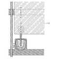
に設けられたコンタクトホールを介して直接接して導通させている。Further, FIGS. 11 (A1) and 11 (A2) show a top view and a cross-sectional view of the gate wiring terminal portion at this stage, respectively. FIG. 11 (A1) corresponds to a cross-sectional view taken along the line C1-C2 in FIG. 11 (A2). In FIG. 11A, the transparent
), In the terminal portion, the
It is in direct contact with each other through a contact hole provided in the above to conduct conduction.
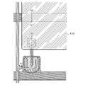
また、図11(B1)、及び図11(B2)は、ソース配線端子部の上面図及び断面図を
それぞれ図示している。また、図11(B1)は図11(B2)中のD1-D2線に沿っ
た断面図に相当する。図11(B1)において、保護絶縁層222上に形成される透明導
電層129は、入力端子として機能する接続用の端子電極である。また、図11(B1)
において、端子部では、ゲート配線と同じ材料で形成される電極156が、ソース配線と
電気的に接続される第2の端子122の下方にゲート絶縁層204を介して重なる場合を
示している。電極156は第2の端子122とは電気的に接続しておらず、電極156を
第2の端子122と異なる電位、例えばフローティング、GND、0Vなどに設定すれば
、ノイズ対策のための容量または静電気対策のための容量を形成することができる。また
、第2の端子122は、保護絶縁層222を介して透明導電層129と電気的に接続して
いる。Further, FIGS. 11 (B1) and 11 (B2) show a top view and a cross-sectional view of the source wiring terminal portion, respectively. Further, FIG. 11 (B1) corresponds to a cross-sectional view taken along the line D1-D2 in FIG. 11 (B2). In FIG. 11B, the transparent
In the terminal portion, an
ゲート配線、ソース配線、及び容量配線は画素密度に応じて複数本設けられるものである
。また、端子部においては、ゲート配線と同電位の第1の端子、ソース配線と同電位の第
2の端子、容量配線と同電位の第3の端子などが複数並べられて配置される。それぞれの
端子の数は、それぞれ任意な数で設ければ良いものとし、実施者が適宣決定すれば良い。A plurality of gate wirings, source wirings, and capacitive wirings are provided according to the pixel density. Further, in the terminal portion, a plurality of first terminals having the same potential as the gate wiring, second terminals having the same potential as the source wiring, and third terminals having the same potential as the capacitive wiring are arranged side by side. The number of each terminal may be any number, and the practitioner may make an appropriate decision.
以上の工程により、6枚のフォトマスクを使用して、ボトムゲート型のnチャネル型薄膜
トランジスタや保持容量等の素子を完成させることができる。そして、これらの素子を個
々の画素に対応してマトリクス状に配置することにより、アクティブマトリクス型の表示
装置を作製するための一方の基板とすることができる。本明細書では便宜上このような基
板をアクティブマトリクス基板と呼ぶ。Through the above steps, it is possible to complete an element such as a bottom gate type n-channel thin film transistor and a holding capacity by using six photomasks. Then, by arranging these elements in a matrix corresponding to each pixel, it can be used as one substrate for manufacturing an active matrix type display device. In the present specification, such a substrate is referred to as an active matrix substrate for convenience.
アクティブマトリクス型の液晶表示装置を作製する場合には、アクティブマトリクス基板
と、対向電極が設けられた対向基板との間に液晶層を設け、アクティブマトリクス基板と
対向基板とを固定する。なお、対向基板に設けられた対向電極と電気的に接続する共通電
極をアクティブマトリクス基板上に設け、共通電極と電気的に接続する第4の端子を端子
部に設ける。この第4の端子は、共通電極を固定電位、例えばGND、0Vなどに設定す
るための端子である。When manufacturing an active matrix type liquid crystal display device, a liquid crystal layer is provided between the active matrix substrate and the facing substrate provided with the counter electrode, and the active matrix substrate and the facing substrate are fixed. A common electrode electrically connected to the counter electrode provided on the counter substrate is provided on the active matrix substrate, and a fourth terminal electrically connected to the common electrode is provided in the terminal portion. This fourth terminal is a terminal for setting the common electrode to a fixed potential, for example, GND, 0V, or the like.
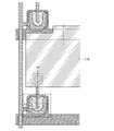
また、本実施の形態で示す構成は、図10の画素構成に限られない。他の構成の一例を図
12に示す。図12は容量配線を設けず、画素電極と、隣接する画素のゲート配線とを電
極とし、保護絶縁層及びゲート絶縁層を誘電体として保持容量を形成する構成を示してい
る。この場合、容量配線及び容量配線と接続する第3の端子は省略することができる。Further, the configuration shown in this embodiment is not limited to the pixel configuration shown in FIG. An example of another configuration is shown in FIG. FIG. 12 shows a configuration in which a pixel electrode and a gate wiring of adjacent pixels are used as electrodes and a protective insulating layer and a gate insulating layer are used as dielectrics to form a holding capacitance without providing a capacitive wiring. In this case, the capacitive wiring and the third terminal connected to the capacitive wiring can be omitted.
なお、本実施の形態は、他の実施の形態と適宜組み合わせて用いることができる。In addition, this embodiment can be used in combination with other embodiments as appropriate.
(実施の形態4)
本実施の形態では、表示装置において、同一基板上に少なくとも駆動回路の一部と、画素
部に配置する薄膜トランジスタを作製する例について以下に説明する。(Embodiment 4)
In the present embodiment, an example of producing at least a part of the drive circuit and a thin film transistor to be arranged in the pixel portion on the same substrate in the display device will be described below.
画素部に配置する薄膜トランジスタは、実施の形態3に従って形成する。また、実施の形
態3に示す薄膜トランジスタはnチャネル型TFTであるため、駆動回路のうち、nチャ
ネル型TFTで構成することができる駆動回路の一部を画素部の薄膜トランジスタと同一
基板上に形成する。The thin film transistor to be arranged in the pixel portion is formed according to the third embodiment. Further, since the thin film transistor shown in the third embodiment is an n-channel type TFT, a part of the drive circuit that can be configured by the n-channel type TFT is formed on the same substrate as the thin film transistor of the pixel portion. ..
表示装置の一例であるアクティブマトリクス型液晶表示装置のブロック図の一例を図14
(A)に示す。図14(A)に示す表示装置は、基板5300上に表示素子を備えた画素
を複数有する画素部5301と、各画素を選択する走査線駆動回路5302と、選択され
た画素へのビデオ信号の入力を制御する信号線駆動回路5303とを有する。FIG. 14 is an example of a block diagram of an active matrix type liquid crystal display device which is an example of a display device.
Shown in (A). The display device shown in FIG. 14A has a pixel unit 5301 having a plurality of pixels having a display element on the
また、実施の形態3に示す薄膜トランジスタは、nチャネル型TFTであり、nチャネル
型TFTで構成する信号線駆動回路について図15を用いて説明する。Further, the thin film transistor shown in the third embodiment is an n-channel type TFT, and a signal line drive circuit configured by the n-channel type TFT will be described with reference to FIG.
図15に示す信号線駆動回路は、ドライバIC5601、スイッチ群5602_1~56
02_M、第1の配線5611、第2の配線5612、第3の配線5613及び配線56
21_1~5621_Mを有する。スイッチ群5602_1~5602_Mそれぞれは、
第1の薄膜トランジスタ5603a、第2の薄膜トランジスタ5603b及び第3の薄膜
トランジスタ5603cを有する。The signal line drive circuit shown in FIG. 15 includes a driver IC5601 and a switch group 5602_1 to 56.
02_M,
It has 21_1 to 5621_M. Switch group 5602_1 to 5602_M respectively
It has a first
ドライバIC5601は第1の配線5611、第2の配線5612、第3の配線5613
及び配線5621_1~5621_Mに接続される。そして、スイッチ群5602_1~
5602_Mそれぞれは、第1の配線5611、第2の配線5612、第3の配線561
3及びスイッチ群5602_1~5602_Mそれぞれに対応した配線5621_1~5
621_Mに接続される。そして、配線5621_1~5621_Mそれぞれは、第1の
薄膜トランジスタ5603a、第2の薄膜トランジスタ5603b及び第3の薄膜トラン
ジスタ5603cを介して、3つの信号線(信号線Sm-2、信号線Sm-1、信号線S
m(m=3M))に接続される。例えば、J列目の配線5621_J(配線5621_1
~配線5621_Mのうちいずれか一)は、スイッチ群5602_Jが有する第1の薄膜
トランジスタ5603a、第2の薄膜トランジスタ5603b及び第3の薄膜トランジス
タ5603cを介して、信号線Sj-2、信号線Sj-1、信号線Sj(j=3J)に接
続される。The
And wiring 5621_1 to 5621_M. And switch group 5602_1 ~
5602_M Each is the
Wiring 5621_1 to 5 corresponding to 3 and switch groups 5602_1 to 5602_M, respectively.
Connected to 621_M. Each of the wirings 5621_1 to 5621_M has three signal lines (signal line Sm-2, signal line Sm-1, signal line S) via the first
It is connected to m (m = 3M)). For example, wiring 5621_J in the Jth column (wiring 5621_1)
The wiring 5621_M) has a signal line Sj-2, a signal line Sj-1, and a signal via the first
なお、第1の配線5611、第2の配線5612、第3の配線5613には、それぞれ信
号が入力される。Signals are input to the
なお、ドライバIC5601は、単結晶半導体を用いて形成されていることが望ましい。
さらに、スイッチ群5602_1~5602_Mは、画素部と同一基板上に形成されてい
ることが望ましい。したがって、ドライバIC5601とスイッチ群5602_1~56
02_MとはFPCなどを介して接続するとよい。又は、画素部と同一基板上に貼り合わ
せなどの方法により形成された単結晶半導体を用いてドライバIC5601を形成しても
良い。It is desirable that the driver IC5601 is formed by using a single crystal semiconductor.
Further, it is desirable that the switch groups 5602_1 to 5602_M are formed on the same substrate as the pixel portion. Therefore, the driver IC5601 and the switch group 5602_1 to 56
It is preferable to connect to 02_M via FPC or the like. Alternatively, the driver IC5601 may be formed by using a single crystal semiconductor formed by a method such as bonding on the same substrate as the pixel portion.
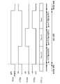
次に、図15に示した信号線駆動回路の動作について、図16のタイミングチャートを参
照して説明する。なお、図16のタイミングチャートは、i行目の走査線Giが選択され
ている場合のタイミングチャートを示している。さらに、i行目の走査線Giの選択期間
は、第1のサブ選択期間T1、第2のサブ選択期間T2及び第3のサブ選択期間T3に分
割されている。さらに、図15の信号線駆動回路は、他の行の走査線が選択されている場
合でも図16と同様の動作をする。Next, the operation of the signal line drive circuit shown in FIG. 15 will be described with reference to the timing chart of FIG. The timing chart of FIG. 16 shows a timing chart when the scanning line Gi on the i-th row is selected. Further, the selection period of the scan line Gi on the i-th row is divided into a first sub-selection period T1, a second sub-selection period T2, and a third sub-selection period T3. Further, the signal line drive circuit of FIG. 15 operates in the same manner as in FIG. 16 even when the scanning lines of other lines are selected.
なお、図16のタイミングチャートは、J列目の配線5621_Jが第1の薄膜トランジ
スタ5603a、第2の薄膜トランジスタ5603b及び第3の薄膜トランジスタ560
3cを介して、信号線Sj-2、信号線Sj-1、信号線Sjに接続される場合について
示している。In the timing chart of FIG. 16, the wiring 5621_J in the Jth column is the first
The case where it is connected to the signal line Sj-2, the signal line Sj-1, and the signal line Sj via 3c is shown.
なお、図16のタイミングチャートは、i行目の走査線Giが選択されるタイミング、第
1の薄膜トランジスタ5603aのオン・オフのタイミング5703a、第2の薄膜トラ
ンジスタ5603bのオン・オフのタイミング5703b、第3の薄膜トランジスタ56
03cのオン・オフのタイミング5703c及びJ列目の配線5621_Jに入力される
信号5721_Jを示している。In the timing chart of FIG. 16, the timing at which the scanning line Gi on the i-th row is selected, the on / off timing 5703a of the first
The on / off timing 5703c of 03c and the signal 5721_J input to the wiring 5621_J in the Jth column are shown.
なお、配線5621_1~配線5621_Mには第1のサブ選択期間T1、第2のサブ選
択期間T2及び第3のサブ選択期間T3において、それぞれ別のビデオ信号が入力される
。例えば、第1のサブ選択期間T1において配線5621_Jに入力されるビデオ信号は
信号線Sj-2に入力され、第2のサブ選択期間T2において配線5621_Jに入力さ
れるビデオ信号は信号線Sj-1に入力され、第3のサブ選択期間T3において配線56
21_Jに入力されるビデオ信号は信号線Sjに入力される。さらに、第1のサブ選択期
間T1、第2のサブ選択期間T2及び第3のサブ選択期間T3において、配線5621_
Jに入力されるビデオ信号をそれぞれData_j-2、Data_j-1、Data_
jとする。Note that different video signals are input to the wiring 5621_1 to the wiring 5621_M in the first subselection period T1, the second subselection period T2, and the third subselection period T3. For example, the video signal input to the wiring 5621_J in the first sub-selection period T1 is input to the signal line Sj-2, and the video signal input to the wiring 5621_J in the second sub-selection period T2 is the signal line Sj-1. Is input to, and wiring 56 in the third sub-selection period T3.
The video signal input to 21_J is input to the signal line Sj. Further, in the first subselection period T1, the second subselection period T2, and the third subselection period T3, the wiring 5621_
The video signals input to J are Data_j-2, Data_j-1, and Data_, respectively.
Let it be j.
図16に示すように、第1のサブ選択期間T1において第1の薄膜トランジスタ5603
aがオンし、第2の薄膜トランジスタ5603b及び第3の薄膜トランジスタ5603c
がオフする。このとき、配線5621_Jに入力されるData_j-2が、第1の薄膜
トランジスタ5603aを介して信号線Sj-2に入力される。第2のサブ選択期間T2
では、第2の薄膜トランジスタ5603bがオンし、第1の薄膜トランジスタ5603a
及び第3の薄膜トランジスタ5603cがオフする。このとき、配線5621_Jに入力
されるData_j-1が、第2の薄膜トランジスタ5603bを介して信号線Sj-1
に入力される。第3のサブ選択期間T3では、第3の薄膜トランジスタ5603cがオン
し、第1の薄膜トランジスタ5603a及び第2の薄膜トランジスタ5603bがオフす
る。このとき、配線5621_Jに入力されるData_jが、第3の薄膜トランジスタ
5603cを介して信号線Sjに入力される。As shown in FIG. 16, the first thin film transistor 5603 in the first subselection period T1.
When a is turned on, the second
Turns off. At this time, Data_j-2 input to the wiring 5621_J is input to the signal line Sj-2 via the first
Then, the second
And the third
Is entered in. In the third subselection period T3, the third
以上のことから、図15の信号線駆動回路は、1ゲート選択期間を3つに分割することで
、1ゲート選択期間中に1つの配線5621から3つの信号線にビデオ信号を入力するこ
とができる。したがって、図15の信号線駆動回路は、ドライバIC5601が形成され
る基板と、画素部が形成されている基板との接続数を信号線の数に比べて約1/3にする
ことができる。接続数が約1/3になることによって、図15の信号線駆動回路は、信頼
性、歩留まりなどを向上できる。From the above, the signal line drive circuit of FIG. 15 can input a video signal from one wiring 5621 to three signal lines during one gate selection period by dividing one gate selection period into three. can. Therefore, in the signal line drive circuit of FIG. 15, the number of connections between the substrate on which the driver IC5601 is formed and the substrate on which the pixel portion is formed can be reduced to about 1/3 of the number of signal lines. By reducing the number of connections to about 1/3, the signal line drive circuit of FIG. 15 can improve reliability, yield, and the like.
なお、図15のように、1ゲート選択期間を複数のサブ選択期間に分割し、複数のサブ選
択期間それぞれにおいて、ある1つの配線から複数の信号線それぞれにビデオ信号を入力
することができれば、薄膜トランジスタの配置や数、駆動方法などは限定されない。As shown in FIG. 15, if one gate selection period can be divided into a plurality of sub-selection periods, and video signals can be input from one wiring to each of a plurality of signal lines in each of the plurality of sub-selection periods. The arrangement and number of thin film transistors and the driving method are not limited.
例えば、3つ以上のサブ選択期間それぞれにおいて1つの配線から3つ以上の信号線それ
ぞれにビデオ信号を入力する場合は、薄膜トランジスタ及び薄膜トランジスタを制御する
ための配線を追加すればよい。ただし、1ゲート選択期間を4つ以上のサブ選択期間に分
割すると、1つのサブ選択期間が短くなる。したがって、1ゲート選択期間は、2つ又は
3つのサブ選択期間に分割されることが望ましい。For example, when a video signal is input from one wiring to each of three or more signal lines in each of three or more sub-selection periods, wiring for controlling the thin film transistor and the thin film transistor may be added. However, if one gate selection period is divided into four or more sub-selection periods, one sub-selection period becomes shorter. Therefore, it is desirable that the one-gate selection period be divided into two or three sub-selection periods.
別の例として、図17のタイミングチャートに示すように、1つの選択期間をプリチャー
ジ期間Tp、第1のサブ選択期間T1、第2のサブ選択期間T2、第3の選択期間T3に
分割してもよい。さらに、図17のタイミングチャートは、i行目の走査線Giが選択さ
れるタイミング、第1の薄膜トランジスタ5603aのオン・オフのタイミング5803
a、第2の薄膜トランジスタ5603bのオン・オフのタイミング5803b、第3の薄
膜トランジスタ5603cのオン・オフのタイミング5803c及びJ列目の配線562
1_Jに入力される信号5821_Jを示している。図17に示すように、プリチャージ
期間Tpにおいて第1の薄膜トランジスタ5603a、第2の薄膜トランジスタ5603
b及び第3の薄膜トランジスタ5603cがオンする。このとき、配線5621_Jに入
力されるプリチャージ電圧Vpが第1の薄膜トランジスタ5603a、第2の薄膜トラン
ジスタ5603b及び第3の薄膜トランジスタ5603cを介してそれぞれ信号線Sj-
2、信号線Sj-1、信号線Sjに入力される。第1のサブ選択期間T1において第1の
薄膜トランジスタ5603aがオンし、第2の薄膜トランジスタ5603b及び第3の薄
膜トランジスタ5603cがオフする。このとき、配線5621_Jに入力されるDat
a_j-2が、第1の薄膜トランジスタ5603aを介して信号線Sj-2に入力される
。第2のサブ選択期間T2では、第2の薄膜トランジスタ5603bがオンし、第1の薄
膜トランジスタ5603a及び第3の薄膜トランジスタ5603cがオフする。このとき
、配線5621_Jに入力されるData_j-1が、第2の薄膜トランジスタ5603
bを介して信号線Sj-1に入力される。第3のサブ選択期間T3では、第3の薄膜トラ
ンジスタ5603cがオンし、第1の薄膜トランジスタ5603a及び第2の薄膜トラン
ジスタ5603bがオフする。このとき、配線5621_Jに入力されるData_jが
、第3の薄膜トランジスタ5603cを介して信号線Sjに入力される。As another example, as shown in the timing chart of FIG. 17, one selection period is divided into a precharge period Tp, a first sub-selection period T1, a second sub-selection period T2, and a third selection period T3. You may. Further, in the timing chart of FIG. 17, the timing at which the scanning line Gi on the i-th row is selected and the on / off timing of the first
a, On / off
The signal 5821_J input to 1_J is shown. As shown in FIG. 17, during the precharge period Tp, the first
b and the third
2. Inputs to the signal line Sj-1 and the signal line Sj. In the first subselection period T1, the first
a_j-2 is input to the signal line Sj-2 via the first
It is input to the signal line Sj-1 via b. In the third subselection period T3, the third
以上のことから、図17のタイミングチャートを適用した図15の信号線駆動回路は、サ
ブ選択期間の前にプリチャージ選択期間を設けることによって、信号線をプリチャージで
きるため、画素へのビデオ信号の書き込みを高速に行うことができる。なお、図17にお
いて、図16と同様なものに関しては共通の符号を用いて示し、同一部分又は同様な機能
を有する部分の詳細な説明は省略する。From the above, the signal line drive circuit of FIG. 15 to which the timing chart of FIG. 17 is applied can precharge the signal line by providing the precharge selection period before the sub-selection period, so that the video signal to the pixel can be obtained. Can be written at high speed. In FIG. 17, the same parts as those in FIG. 16 are shown by using a common reference numeral, and detailed description of the same part or the part having the same function will be omitted.
また、走査線駆動回路の構成について説明する。走査線駆動回路は、シフトレジスタ、バ
ッファを有している。また場合によってはレベルシフタを有していても良い。走査線駆動
回路において、シフトレジスタにクロック信号(CLK)及びスタートパルス信号(SP
)が入力されることによって、選択信号が生成される。生成された選択信号はバッファに
おいて緩衝増幅され、対応する走査線に供給される。走査線には、1ライン分の画素のト
ランジスタのゲート電極が接続されている。そして、1ライン分の画素のトランジスタを
一斉にONにしなくてはならないので、バッファは大きな電流を流すことが可能なものが
用いられる。Further, the configuration of the scanning line drive circuit will be described. The scanning line drive circuit has a shift register and a buffer. In some cases, it may have a level shifter. In the scan line drive circuit, the clock signal (CLK) and start pulse signal (SP) are stored in the shift register.
) Is input to generate a selection signal. The generated selection signal is buffered and amplified in the buffer and fed to the corresponding scan line. A gate electrode of a transistor having pixels for one line is connected to the scanning line. Since the transistors of one line of pixels must be turned on all at once, a buffer capable of passing a large current is used.
走査線駆動回路の一部に用いるシフトレジスタの一形態について図18及び図19を用い
て説明する。A form of a shift register used as a part of the scanning line drive circuit will be described with reference to FIGS. 18 and 19.
図18にシフトレジスタの回路構成を示す。図18に示すシフトレジスタは、フリップフ
ロップ5701_1~5701_nという複数のフリップフロップで構成される。また、
第1のクロック信号、第2のクロック信号、スタートパルス信号、リセット信号が入力さ
れて動作する。FIG. 18 shows the circuit configuration of the shift register. The shift register shown in FIG. 18 is composed of a plurality of flip-flops 5701_1 to 5701_n. also,
The first clock signal, the second clock signal, the start pulse signal, and the reset signal are input and operated.
図18のシフトレジスタの接続関係について説明する。1段目のフリップフロップ570
1_1は、第1の配線5711、第2の配線5712、第4の配線5714、第5の配線
5715、第7の配線5717_1、及び第7の配線5717_2と接続される。また、
2段目のフリップフロップ5701_2は、第3の配線5713、第4の配線5714、
第5の配線5715、第7の配線5717_1、第7の配線5717_2及び第7の配線
5717_3と接続される。The connection relationship of the shift register of FIG. 18 will be described. 1st stage flip-flop 570
1_1 is connected to the
The second-stage flip-flop 5701_2 has a
It is connected to the
同様に、i段目のフリップフロップ5701_i(フリップフロップ5701_1~57
01_nのうちいずれか一)は、第2の配線5712又は第3の配線5713の一方、第
4の配線5714、第5の配線5715、第7の配線5717_i-1、第7の配線57
17_i、及び第7の配線5717_i+1と接続される。ここで、iが奇数の場合には
、i段目のフリップフロップ5701_iは第2の配線5712と接続され、iが偶数で
ある場合には、i段目のフリップフロップ5701_iは第3の配線5713と接続され
ることになる。Similarly, the i-stage flip-flop 5701_i (flip-flops 5701_1 to 57)
One of 01_n) is one of the
It is connected to 17_i and the seventh
また、n段目のフリップフロップ5701_nは、第2の配線5712又は第3の配線5
713の一方、第4の配線5714、第5の配線5715、第7の配線5717_n-1
、第7の配線5717_n、及び第6の配線5716と接続される。Further, the flip-flop 5701_n in the nth stage is the
On the other hand of 713, the
, 7th wiring 5717_n, and
なお、第1の配線5711、第2の配線5712、第3の配線5713、第6の配線57
16を、それぞれ第1の信号線、第2の信号線、第3の信号線、第4の信号線と呼んでも
よい。さらに、第4の配線5714、第5の配線5715を、それぞれ第1の電源線、第
2の電源線と呼んでもよい。The
16 may be referred to as a first signal line, a second signal line, a third signal line, and a fourth signal line, respectively. Further, the
次に、図18に示すフリップフロップの詳細について、図19を用いて説明する。図19
に示すフリップフロップは、第1の薄膜トランジスタ5571、第2の薄膜トランジスタ
5572、第3の薄膜トランジスタ5573、第4の薄膜トランジスタ5574、第5の
薄膜トランジスタ5575、第6の薄膜トランジスタ5576、第7の薄膜トランジスタ
5577及び第8の薄膜トランジスタ5578を有する。なお、第1の薄膜トランジスタ
5571、第2の薄膜トランジスタ5572、第3の薄膜トランジスタ5573、第4の
薄膜トランジスタ5574、第5の薄膜トランジスタ5575、第6の薄膜トランジスタ
5576、第7の薄膜トランジスタ5577及び第8の薄膜トランジスタ5578は、n
チャネル型トランジスタであり、ゲート・ソース間電圧(Vgs)がしきい値電圧(Vt
h)を上回ったとき導通状態になるものとする。Next, the details of the flip-flop shown in FIG. 18 will be described with reference to FIG. FIG. 19
The flip-flops shown in the above are the first
It is a channel type transistor, and the gate-source voltage (Vgs) is the threshold voltage (Vt).
When it exceeds h), it shall be in a conductive state.
また、図19に示すフリップフロップは、第1の配線5501、第2の配線5502、第
3の配線5503、第4の配線5504、第5の配線5505、及び第6の配線5506
を有する。Further, the flip-flop shown in FIG. 19 has a
Have.
なお、ここでは全ての薄膜トランジスタを、エンハンスメント型のnチャネル型トランジ
スタとする例を示すが、特に限定されず、例えば、デプレッション型のnチャネル型トラ
ンジスタを用いて駆動回路を駆動させることもできる。Here, an example in which all the thin film transistors are used as enhancement type n-channel transistors is shown, but the present invention is not particularly limited, and for example, a drive circuit can be driven by using a depletion type n-channel transistors.
次に、図18に示すフリップフロップの接続構成について、以下に示す。Next, the connection configuration of the flip-flop shown in FIG. 18 is shown below.
第1の薄膜トランジスタ5571の第1の電極(ソース電極またはドレイン電極の一方)
が第4の配線5504に接続され、第2の電極(ソース電極またはドレイン電極の他方)
が第3の配線5503に接続される。First electrode of the first thin film transistor 5571 (one of the source electrode and the drain electrode)
Is connected to the
Is connected to the
第2の薄膜トランジスタ5572の第1の電極が第6の配線5506に接続され、第2の
電極が第3の配線5503に接続される。The first electrode of the second
第3の薄膜トランジスタ5573の第1の電極及びゲート電極が第5の配線5505に接
続され、第2の電極が第2の薄膜トランジスタ5572のゲート電極に接続される。The first electrode and the gate electrode of the third
第4の薄膜トランジスタ5574の第1の電極が第6の配線5506に接続され、ゲート
電極が第1の薄膜トランジスタ5571のゲート電極に接続され、第2の電極が第2の薄
膜トランジスタ5572のゲート電極に接続される。The first electrode of the fourth
第5の薄膜トランジスタ5575の第1の電極が第5の配線5505に接続され、ゲート
電極が第1の配線5501に接続され、第2の電極が第1の薄膜トランジスタ5571の
ゲート電極に接続される。The first electrode of the fifth
第6の薄膜トランジスタ5576の第1の電極が第6の配線5506に接続され、ゲート
電極が第2の薄膜トランジスタ5572のゲート電極に接続され、第2の電極が第1の薄
膜トランジスタ5571のゲート電極に接続される。The first electrode of the sixth
第7の薄膜トランジスタ5577の第1の電極が第6の配線5506に接続され、ゲート
電極が第2の配線5502に接続され、第2の電極が第1の薄膜トランジスタ5571の
ゲート電極に接続される。The first electrode of the seventh
第8の薄膜トランジスタ5578の第1の電極が第6の配線5506に接続され、ゲート
電極が第1の配線5501に接続され、第2の電極が第2の薄膜トランジスタ5572の
ゲート電極に接続される。The first electrode of the eighth
なお、第1の薄膜トランジスタ5571のゲート電極、第4の薄膜トランジスタ5574
のゲート電極、第5の薄膜トランジスタ5575の第2の電極、第6の薄膜トランジスタ
5576の第2の電極及び第7の薄膜トランジスタ5577の第2の電極の接続箇所をノ
ード5543とする。さらに、第2の薄膜トランジスタ5572のゲート電極、第3の薄
膜トランジスタ5573の第2の電極、第4の薄膜トランジスタ5574の第2の電極、
第6の薄膜トランジスタ5576のゲート電極及び第8の薄膜トランジスタ5578の第
2の電極の接続箇所をノード5544とする。The gate electrode of the first
The connection point of the gate electrode, the second electrode of the fifth
The connection point between the gate electrode of the sixth
なお、第1の配線5501、第2の配線5502、第3の配線5503及び第4の配線5
504を、それぞれ第1の信号線、第2の信号線、第3の信号線、第4の信号線と呼んで
もよい。さらに、第5の配線5505を第1の電源線、第6の配線5506を第2の電源
線と呼んでもよい。The
504 may be referred to as a first signal line, a second signal line, a third signal line, and a fourth signal line, respectively. Further, the
i段目のフリップフロップ5701_iにおいて、図19中の第1の配線5501と、図
18中の第7の配線5717_i-1が接続される。また、図19中の第2の配線550
2と、図18中の第7の配線5717_i+1が接続される。また、図19中の第3の配
線5503と、第7の配線5717_iが接続される。さらに、図19中の第6の配線5
506と、第5の配線5715が接続される。In the flip-flop 5701_i of the i-th stage, the
2 and the seventh wiring 5717_i + 1 in FIG. 18 are connected. Further, the
The 506 and the
iが奇数の場合、図19中の第4の配線5504は、図18中の第2の配線5712と接
続され、iが偶数の場合、図18中の第3の配線5713と接続される。また、図19中
の第5の配線5505と、図18中の第4の配線5714が接続される。If i is odd, the
ただし、1段目のフリップフロップ5701_1において、図19中の第1の配線550
1は図18中の第1の配線5711に接続される。また、n段目のフリップフロップ57
01_nにおいて、図19中の第2の配線5502は図18中の第6の配線5716に接
続される。However, in the first-stage flip-flop 5701_1, the first wiring 550 in FIG. 19
1 is connected to the
At 01_n, the
なお、信号線駆動回路及び走査線駆動回路を実施の形態3に示すnチャネル型TFTのみ
で作製することも可能である。実施の形態3に示すnチャネル型TFTはトランジスタの
移動度が大きいため、駆動回路の駆動周波数を高くすることが可能となる。また、実施の
形態3に示すnチャネル型TFTはIn-Ga-Zn-O系非単結晶膜であるソース領域
又はドレイン領域により寄生容量が低減されるため、周波数特性(f特性と呼ばれる)が
高い。例えば、実施の形態3に示すnチャネル型TFTを用いた走査線駆動回路は、高速
に動作させることができるため、フレーム周波数を高くすること、または、黒画面挿入を
実現することなども実現することができる。It is also possible to manufacture the signal line drive circuit and the scanning line drive circuit using only the n-channel TFT shown in the third embodiment. Since the n-channel TFT shown in the third embodiment has high mobility of the transistor, it is possible to increase the drive frequency of the drive circuit. Further, the n-channel TFT shown in the third embodiment has a frequency characteristic (called f characteristic) because the parasitic capacitance is reduced by the source region or the drain region which is an In—Ga—Zn—O system non-single crystal film. expensive. For example, since the scanning line drive circuit using the n-channel TFT shown in the third embodiment can be operated at high speed, it is possible to increase the frame frequency or realize black screen insertion. be able to.
さらに、走査線駆動回路のトランジスタのチャネル幅を大きくすることや、複数の走査線
駆動回路を配置することなどによって、さらに高いフレーム周波数を実現することができ
る。複数の走査線駆動回路を配置する場合は、例えば、偶数行の走査線を駆動する為の走
査線駆動回路を片側に配置し、奇数行の走査線を駆動するための走査線駆動回路をその反
対側に配置することにより、フレーム周波数を高くすることができる。また、複数の走査
線駆動回路により、同じ走査線に信号を出力すると、表示装置の大型化に有利である。Further, a higher frame frequency can be realized by increasing the channel width of the transistor of the scanning line driving circuit, arranging a plurality of scanning line driving circuits, and the like. When arranging a plurality of scanning line driving circuits, for example, a scanning line driving circuit for driving even-numbered rows of scanning lines is arranged on one side, and a scanning line driving circuit for driving odd-numbered rows of scanning lines is provided. By arranging it on the opposite side, the frame frequency can be increased. Further, if a signal is output to the same scanning line by a plurality of scanning line driving circuits, it is advantageous for increasing the size of the display device.
また、表示装置の一例であるアクティブマトリクス型発光表示装置を作製する場合、少な
くとも一つの画素に複数の薄膜トランジスタを配置するため、走査線駆動回路を複数配置
することが好ましい。アクティブマトリクス型発光表示装置のブロック図の一例を図14
(B)に示す。Further, in the case of manufacturing an active matrix type light emitting display device which is an example of a display device, it is preferable to arrange a plurality of scanning line drive circuits in order to arrange a plurality of thin film transistors in at least one pixel. FIG. 14 is an example of a block diagram of an active matrix type light emission display device.
Shown in (B).
図14(B)に示す発光表示装置は、基板5400上に表示素子を備えた画素を複数有す
る画素部5401と、各画素を選択する第1の走査線駆動回路5402及び第2の走査線
駆動回路5404と、選択された画素へのビデオ信号の入力を制御する信号線駆動回路5
403とを有する。The light emitting display device shown in FIG. 14B has a pixel unit 5401 having a plurality of pixels having a display element on the
It has 403 and.
図14(B)に示す発光表示装置の画素に入力されるビデオ信号をデジタル形式とする場
合、画素はトランジスタのオンとオフの切り替えによって、発光もしくは非発光の状態と
なる。よって、面積階調法または時間階調法を用いて階調の表示を行うことができる。面
積階調法は、1画素を複数の副画素に分割し、各副画素を独立にビデオ信号に基づいて駆
動させることによって、階調表示を行う駆動法である。また時間階調法は、画素が発光す
る期間を制御することによって、階調表示を行う駆動法である。When the video signal input to the pixels of the light emitting display device shown in FIG. 14B is in the digital format, the pixels are in a light emitting state or a non-light emitting state by switching the transistor on and off. Therefore, the gradation can be displayed by using the area gradation method or the time gradation method. The area gradation method is a driving method for displaying gradation by dividing one pixel into a plurality of sub-pixels and driving each sub-pixel independently based on a video signal. Further, the time gradation method is a driving method for displaying gradation by controlling the period during which the pixels emit light.
発光素子は、液晶素子などに比べて応答速度が高いので、液晶素子よりも時間階調法に適
している。時間階調法で表示を行なう場合、1フレーム期間を複数のサブフレーム期間に
分割する。そしてビデオ信号に従い、各サブフレーム期間において画素の発光素子を発光
または非発光の状態にする。複数のサブフレーム期間に分割することによって、1フレー
ム期間中に画素が発光する期間の合計の長さを、ビデオ信号により制御することができ、
階調を表示することができる。Since the light emitting element has a higher response speed than the liquid crystal element or the like, it is more suitable for the time gradation method than the liquid crystal element. When displaying by the time gradation method, one frame period is divided into a plurality of subframe periods. Then, according to the video signal, the light emitting element of the pixel is put into a light emitting state or a non-light emitting state in each subframe period. By dividing into a plurality of subframe periods, the total length of the period during which the pixels emit light during one frame period can be controlled by the video signal.
The gradation can be displayed.
なお、図14(B)に示す発光表示装置では、一つの画素に2つのスイッチング用TFT
を配置する場合であって、一方のスイッチング用TFTのゲート配線である第1の走査線
に入力される信号を第1走査線駆動回路5402で生成し、他方のスイッチング用TFT
のゲート配線である第2の走査線に入力される信号を第2の走査線駆動回路5404で生
成する例を示しているが、第1の走査線に入力される信号と、第2の走査線に入力される
信号とを、共に1つの走査線駆動回路で生成するようにしても良い。また、例えば、1つ
の画素が有するスイッチング用TFTの数によって、スイッチング素子の動作を制御する
ために用いられる走査線が、各画素に複数設けられることもあり得る。この場合、複数の
走査線に入力される信号を、全て1つの走査線駆動回路で生成しても良いし、複数の各走
査線駆動回路で生成しても良い。In the light emitting display device shown in FIG. 14B, two switching TFTs are used for one pixel.
Is to be arranged, a signal input to the first scanning line, which is the gate wiring of one switching TFT, is generated by the first scanning
Although an example of generating a signal input to the second scanning line, which is the gate wiring of the above, by the second scanning
また、発光表示装置においても、駆動回路のうち、nチャネル型TFTで構成することが
できる駆動回路の一部を画素部の薄膜トランジスタと同一基板上に形成することができる
。また、信号線駆動回路及び走査線駆動回路を実施の形態3に示すnチャネル型TFTの
みで作製することも可能である。Further, also in the light emission display device, a part of the drive circuit that can be configured by the n-channel type TFT can be formed on the same substrate as the thin film transistor of the pixel portion. Further, it is also possible to manufacture the signal line drive circuit and the scanning line drive circuit only by the n-channel type TFT shown in the third embodiment.
また、上述した駆動回路は、液晶表示装置や発光表示装置に限らず、スイッチング素子と
電気的に接続する素子を利用して電子インクを駆動させる電子ペーパーに用いてもよい。
電子ペーパーは、電気泳動表示装置(電気泳動ディスプレイ)とも呼ばれており、紙と同
じ読みやすさを実現し、他の表示装置に比べ消費電力を抑え、且つ、薄型、軽量とするこ
とが可能である。Further, the drive circuit described above is not limited to the liquid crystal display device and the light emission display device, and may be used for electronic paper for driving electronic ink by using an element electrically connected to a switching element.
Electronic paper is also called an electrophoresis display device (electrophoresis display), which realizes the same readability as paper, consumes less power than other display devices, and can be made thinner and lighter. Is.
電気泳動ディスプレイは、様々な形態が考えられ得るが、例えば、プラスの電荷を有する
第1の粒子と、マイナスの電荷を有する第2の粒子とを含むマイクロカプセルが溶媒また
は溶質に複数分散された構成とすることができ、この場合、マイクロカプセルに電界を印
加することによって、マイクロカプセル中の粒子を互いに反対方向に移動させて一方側に
集合した粒子の色のみを表示することができる。なお、第1の粒子または第2の粒子は染
料を含み、電界がない場合において移動しないものである。また、第1の粒子の色と第2
の粒子の色は異なるもの(無色を含む)とする。The electrophoretic display may take various forms, for example, a plurality of microcapsules containing a first particle having a positive charge and a second particle having a negative charge dispersed in a solvent or a solute. In this case, by applying an electric charge to the microcapsules, the particles in the microcapsules can be moved in opposite directions and only the color of the particles aggregated on one side can be displayed. The first particle or the second particle contains a dye and does not move in the absence of an electric field. Also, the color of the first particle and the second
The color of the particles of is different (including colorless).
このように、電気泳動ディスプレイは、電界などにより微粒子が移動する機構を利用した
ディスプレイである。電気泳動ディスプレイでは、液晶表示装置には必要な偏光板や、対
向基板が不要であり、厚さや重さを著しく低減することができる。As described above, the electrophoresis display is a display utilizing a mechanism in which fine particles move due to an electric field or the like. The electrophoretic display does not require a polarizing plate or a facing substrate, which is necessary for a liquid crystal display device, and the thickness and weight can be significantly reduced.
上記マイクロカプセルを溶媒中に分散させたものが電子インクと呼ばれるものであり、こ
の電子インクはガラス、プラスチック、布、紙などの表面に印刷することができる。また
、カラーフィルタや色素を有する粒子を用いることによってカラー表示も可能である。The microcapsules dispersed in a solvent are called electronic inks, and the electronic inks can be printed on the surface of glass, plastic, cloth, paper, or the like. In addition, color display is also possible by using a color filter or particles having a dye.
アクティブマトリクス基板上にマイクロカプセルを複数配置して、アクティブマトリクス
基板に形成された電極と別の電極とでマイクロカプセルを挟み込むことによりアクティブ
マトリクス型の表示装置が完成し、マイクロカプセルに電界を印加すれば表示を行うこと
ができる。アクティブマトリクス基板としては、例えば、実施の形態3の薄膜トランジス
タによって得られるアクティブマトリクス基板を用いることができる。An active matrix type display device is completed by arranging a plurality of microcapsules on an active matrix substrate and sandwiching the microcapsules between an electrode formed on the active matrix substrate and another electrode, and an electric field is applied to the microcapsules. Can be displayed. As the active matrix substrate, for example, the active matrix substrate obtained by the thin film transistor of the third embodiment can be used.
なお、マイクロカプセル中の第1の粒子および第2の粒子は、導電体材料、絶縁体材料、
半導体材料、磁性材料、液晶材料、強誘電性材料、エレクトロルミネセント材料、エレク
トロクロミック材料、磁気泳動材料から選ばれた一種の材料、またはこれらの複合材料を
用いればよい。The first particles and the second particles in the microcapsules are a conductor material, an insulator material, and the like.
A semiconductor material, a magnetic material, a liquid crystal material, a ferroelectric material, an electroluminescent material, an electrochromic material, a kind of material selected from a magnetic migration material, or a composite material thereof may be used.
以上の工程により、半導体装置として信頼性の高い表示装置を作製することができる。Through the above steps, a highly reliable display device can be manufactured as a semiconductor device.
本実施の形態は、他の実施の形態に記載した構成と適宜組み合わせて実施することが可能
である。This embodiment can be implemented in combination with the configurations described in other embodiments as appropriate.
(実施の形態5)
本実施の形態では、薄膜トランジスタを作製し、該薄膜トランジスタを画素部、さらには
駆動回路に用いて表示機能を有する半導体装置(表示装置ともいう)を作製する場合につ
いて説明する。また、薄膜トランジスタを、駆動回路の一部または全体を、画素部と同じ
基板上に一体形成し、システムオンパネルを形成することができる。(Embodiment 5)
In the present embodiment, a case where a thin film transistor is manufactured and the thin film transistor is used in a pixel portion and further in a drive circuit to manufacture a semiconductor device (also referred to as a display device) having a display function will be described. Further, the thin film transistor can be integrally formed on a part or the whole of the drive circuit on the same substrate as the pixel portion to form a system-on-panel.
表示装置は表示素子を含む。表示素子としては液晶素子(液晶表示素子ともいう)、発光
素子(発光表示素子ともいう)を用いることができる。発光素子は、電流または電圧によ
って輝度が制御される素子をその範疇に含んでおり、具体的には無機EL(Electr
o Luminescence)、有機EL等が含まれる。また、電子インクなど、電気
的作用によりコントラストが変化する表示媒体も適用することができる。The display device includes a display element. As the display element, a liquid crystal element (also referred to as a liquid crystal display element) or a light emitting element (also referred to as a light emitting display element) can be used. The light emitting element includes an element whose brightness is controlled by a current or a voltage in the category, and specifically, an inorganic EL (Electr).
o Luminescence), organic EL and the like are included. Further, a display medium whose contrast changes due to an electric action, such as electronic ink, can also be applied.
また、表示装置は、表示素子が封止された状態にあるパネルと、該パネルにコントローラ
を含むIC等を実装した状態にあるモジュールとを含む。さらに表示装置は、該表示装置
を作製する過程における、表示素子が完成する前の一形態に相当する素子基板に関し、該
素子基板は、電流を表示素子に供給するための手段を複数の各画素に備える。素子基板は
、具体的には、表示素子の画素電極のみが形成された状態であっても良いし、画素電極と
なる導電膜を成膜した後であって、エッチングして画素電極を形成する前の状態であって
も良いし、あらゆる形態があてはまる。Further, the display device includes a panel in which the display element is sealed, and a module in which an IC or the like including a controller is mounted on the panel. Further, the display device relates to an element substrate corresponding to a form before the display element is completed in the process of manufacturing the display device, and the element substrate provides means for supplying a current to the display element in each of a plurality of pixels. Prepare for. Specifically, the element substrate may be in a state in which only the pixel electrode of the display element is formed, or after the conductive film to be the pixel electrode is formed, the pixel electrode is formed by etching. It may be in the previous state, and all forms apply.
なお、本明細書中における表示装置とは、画像表示デバイス、表示デバイス、もしくは光
源(照明装置含む)を指す。また、コネクター、例えばFPC(Flexible pr
inted circuit)もしくはTAB(Tape Automated Bon
ding)テープもしくはTCP(Tape Carrier Package)が取り
付けられたモジュール、TABテープやTCPの先にプリント配線板が設けられたモジュ
ール、または表示素子にCOG(Chip On Glass)方式によりIC(集積回
路)が直接実装されたモジュールも全て表示装置に含むものとする。The display device in the present specification refers to an image display device, a display device, or a light source (including a lighting device). Also, a connector such as FPC (Flexible pr)
integrated cycle) or TAB (Tape Automated Bon)
A module with a ding) tape or TCP (Tape Carrier Package) attached, a module with a printed wiring board at the end of a TAB tape or TCP, or an IC (integrated circuit) on the display element by the COG (Chip On Glass) method. All directly mounted modules shall be included in the display device.
本実施の形態では、半導体装置として液晶表示装置の例を示す。まず、半導体装置の一形
態に相当する液晶表示パネルの外観及び断面について、図22を用いて説明する。図22
は、第1の基板4001上に形成された実施の形態3で示したIn-Ga-Zn-O系非
単結晶膜を半導体層として含む信頼性の高い薄膜トランジスタ4010、4011、及び
液晶素子4013を、第2の基板4006との間にシール材4005によって封止した、
パネルの上面図であり、図22(B)は、図22(A1)(A2)のM-Nにおける断面
図に相当する。In this embodiment, an example of a liquid crystal display device as a semiconductor device is shown. First, the appearance and cross section of the liquid crystal display panel corresponding to one form of the semiconductor device will be described with reference to FIG. 22. FIG. 22
A highly reliable
It is a top view of the panel, and FIG. 22 (B) corresponds to a cross-sectional view taken along the line MN of FIGS. 22 (A1) and 22 (A2).
第1の基板4001上に設けられた画素部4002と、走査線駆動回路4004とを囲む
ようにして、シール材4005が設けられている。また画素部4002と、走査線駆動回
路4004の上に第2の基板4006が設けられている。よって画素部4002と、走査
線駆動回路4004とは、第1の基板4001とシール材4005と第2の基板4006
とによって、液晶層4008と共に封止されている。また第1の基板4001上のシール
材4005によって囲まれている領域とは異なる領域に、別途用意された基板上に単結晶
半導体膜又は多結晶半導体膜で形成された信号線駆動回路4003が実装されている。A sealing
It is sealed together with the
なお、別途形成した駆動回路の接続方法は、特に限定されるものではなく、COG方法、
ワイヤボンディング方法、或いはTAB方法などを用いることができる。図22(A1)
は、COG方法により信号線駆動回路4003を実装する例であり、図22(A2)は、
TAB方法により信号線駆動回路4003を実装する例である。The method of connecting the separately formed drive circuit is not particularly limited, and the COG method can be used.
A wire bonding method, a TAB method, or the like can be used. FIG. 22 (A1)
Is an example of mounting the signal
This is an example of mounting the signal
また、第1の基板4001上に設けられた画素部4002と、走査線駆動回路4004は
、薄膜トランジスタを複数有しており、図22(B)では、画素部4002に含まれる薄
膜トランジスタ4010と、走査線駆動回路4004に含まれる薄膜トランジスタ401
1とを例示している。薄膜トランジスタ4010、4011上には絶縁層4020、40
21が設けられている。Further, the
1 and are illustrated. Insulating
21 is provided.
薄膜トランジスタ4010、4011は、In-Ga-Zn-O系非単結晶膜を半導体層
として含む信頼性の高い実施の形態3に示す薄膜トランジスタを適用することができる。
本実施の形態において、薄膜トランジスタ4010、4011はnチャネル型薄膜トラン
ジスタである。As the
In the present embodiment, the
また、液晶素子4013が有する画素電極層4030は、薄膜トランジスタ4010と電
気的に接続されている。そして液晶素子4013の対向電極層4031は第2の基板40
06上に形成されている。画素電極層4030と対向電極層4031と液晶層4008と
が重なっている部分が、液晶素子4013に相当する。なお、画素電極層4030、対向
電極層4031はそれぞれ配向膜として機能する絶縁層4032、4033が設けられ、
絶縁層4032、4033を介して液晶層4008を挟持している。Further, the
It is formed on 06. The portion where the
The
なお、第1の基板4001、第2の基板4006としては、ガラス、金属(代表的にはス
テンレス)、セラミックス、プラスチックを用いることができる。プラスチックとしては
、FRP(Fiberglass-Reinforced Plastics)板、PV
F(ポリビニルフルオライド)フィルム、ポリエステルフィルム、またはアクリル樹脂フ
ィルムを用いることができる。また、アルミニウムホイルをPVFフィルムやポリエステ
ルフィルムで挟んだ構造のシートを用いることもできる。As the
An F (polyvinyl fluoride) film, a polyester film, or an acrylic resin film can be used. Further, a sheet having a structure in which aluminum foil is sandwiched between a PVC film or a polyester film can also be used.
また、4035は絶縁膜を選択的にエッチングすることで得られる柱状のスペーサであり
、画素電極層4030と対向電極層4031との間の距離(セルギャップ)を制御するた
めに設けられている。なお球状のスペーサを用いていても良い。また、対向電極層403
1は、薄膜トランジスタ4010と同一基板上に設けられる共通電位線と電気的に接続さ
れる。共通接続部を用いて、一対の基板間に配置される導電性粒子を介して対向電極層4
031と共通電位線とを電気的に接続することができる。なお、導電性粒子はシール材4
005に含有させる。Further, 4035 is a columnar spacer obtained by selectively etching the insulating film, and is provided to control the distance (cell gap) between the
1 is electrically connected to a common potential line provided on the same substrate as the
The 031 and the common potential line can be electrically connected. The conductive particles are the sealing material 4
It is contained in 005.
また、配向膜を用いないブルー相を示す液晶を用いてもよい。ブルー相は液晶相の一つで
あり、コレステリック液晶を昇温していくと、コレステリック相から等方相へ転移する直
前に発現する相である。ブルー相は狭い温度範囲でしか発現しないため、温度範囲を改善
するために5重量%以上のカイラル剤を混合させた液晶組成物を用いて液晶層4008に
用いる。ブルー相を示す液晶とカイラル剤とを含む液晶組成物は、応答速度が10μs~
100μsと短く、光学的等方性であるため配向処理が不要であり、視野角依存性が小さ
い。Further, a liquid crystal showing a blue phase without using an alignment film may be used. The blue phase is one of the liquid crystal phases, and is a phase that appears immediately before the transition from the cholesteric phase to the isotropic phase when the temperature of the cholesteric liquid crystal is raised. Since the blue phase is expressed only in a narrow temperature range, a liquid crystal composition mixed with 5% by weight or more of a chiral agent is used for the
Since it is as short as 100 μs and is optically isotropic, no orientation treatment is required and the viewing angle dependence is small.
なお、本実施の形態で示す液晶表示装置は透過型液晶表示装置の例であるが、液晶表示装
置は反射型液晶表示装置でも半透過型液晶表示装置でも適用できる。Although the liquid crystal display device shown in this embodiment is an example of a transmissive liquid crystal display device, the liquid crystal display device can be applied to either a reflective liquid crystal display device or a semi-transmissive liquid crystal display device.
また、本実施の形態で示す液晶表示装置では、基板の外側(視認側)に偏光板を設け、内
側に着色層、表示素子に用いる電極層という順に設ける例を示すが、偏光板は基板の内側
に設けてもよい。また、偏光板と着色層の積層構造も本実施の形態に限定されず、偏光板
及び着色層の材料や作製工程条件によって適宜設定すればよい。また、ブラックマトリク
スとして機能する遮光膜を設けてもよい。Further, in the liquid crystal display device shown in the present embodiment, an example is shown in which a polarizing plate is provided on the outside (visual side) of the substrate, a colored layer is provided on the inside, and an electrode layer used for the display element is provided in this order. It may be provided inside. Further, the laminated structure of the polarizing plate and the colored layer is not limited to the present embodiment, and may be appropriately set depending on the material of the polarizing plate and the colored layer and the manufacturing process conditions. Further, a light-shielding film that functions as a black matrix may be provided.
また、本実施の形態では、薄膜トランジスタの表面凹凸を低減するため、及び薄膜トラン
ジスタの信頼性を向上させるため、実施の形態3で得られた薄膜トランジスタを保護膜や
平坦化絶縁膜として機能する絶縁層(絶縁層4020、絶縁層4021)で覆う構成とな
っている。なお、保護膜は、大気中に浮遊する有機物や金属物、水蒸気などの汚染不純物
の侵入を防ぐためのものであり、緻密な膜が好ましい。保護膜は、スパッタ法を用いて、
酸化珪素膜、窒化珪素膜、酸化窒化珪素膜、窒化酸化珪素膜、酸化アルミニウム膜、窒化
アルミニウム膜、酸化窒化アルミニウム膜、又は窒化酸化アルミニウム膜の単層、又は積
層で形成すればよい。本実施の形態では保護膜をスパッタ法で形成する例を示すが、特に
限定されず種々の方法で形成すればよい。Further, in the present embodiment, in order to reduce the surface unevenness of the thin film transistor and to improve the reliability of the thin film transistor, the thin film transistor obtained in the third embodiment is used as an insulating layer (a protective film or a flattening insulating film). It is configured to be covered with an insulating
It may be formed by a single layer or a laminate of a silicon oxide film, a silicon nitride film, a silicon nitride film, a silicon nitride film, an aluminum oxide film, an aluminum nitride film, an aluminum nitride film, or an aluminum nitride film. In this embodiment, an example in which the protective film is formed by a sputtering method is shown, but it is not particularly limited and may be formed by various methods.
ここでは、保護膜として積層構造の絶縁層4020を形成する。ここでは、絶縁層402
0の一層目として、スパッタ法を用いて酸化珪素膜を形成する。保護膜として酸化珪素膜
を用いると、ソース電極層及びドレイン電極層として用いるアルミニウム膜のヒロック防
止に効果がある。Here, an insulating
As the first layer of 0, a silicon oxide film is formed by using a sputtering method. When a silicon oxide film is used as the protective film, it is effective in preventing chilling of the aluminum film used as the source electrode layer and the drain electrode layer.
また、保護膜の二層目として絶縁層を形成する。ここでは、ここでは、絶縁層4020の
二層目として、スパッタ法を用いて窒化珪素膜を形成する。保護膜として窒化珪素膜を用
いると、ナトリウム等の可動イオンが半導体領域中に侵入して、TFTの電気特性を変化
させることを抑制することができる。In addition, an insulating layer is formed as the second layer of the protective film. Here, as the second layer of the insulating
また、保護膜を形成した後に、半導体層のアニール(300℃~400℃)を行ってもよ
い。Further, after forming the protective film, the semiconductor layer may be annealed (300 ° C to 400 ° C).
また、平坦化絶縁膜として絶縁層4021を形成する。絶縁層4021としては、ポリイ
ミド、アクリル、ベンゾシクロブテン、ポリアミド、エポキシ等の、耐熱性を有する有機
材料を用いることができる。また上記有機材料の他に、低誘電率材料(low-k材料)
、シロキサン系樹脂、PSG(リンガラス)、BPSG(リンボロンガラス)等を用いる
ことができる。なお、これらの材料で形成される絶縁膜を複数積層させることで、絶縁層
4021を形成してもよい。Further, the insulating
, Siloxane resin, PSG (phosphorus glass), BPSG (phosphorus glass) and the like can be used. The insulating
なおシロキサン系樹脂とは、シロキサン系材料を出発材料として形成されたSi-O-S
i結合を含む樹脂に相当する。シロキサン系樹脂は置換基としては有機基(例えばアルキ
ル基やアリール基)やフルオロ基を用いても良い。また、有機基はフルオロ基を有してい
ても良い。The siloxane-based resin is Si—O—S formed from a siloxane-based material as a starting material.
It corresponds to a resin containing i-bond. As the substituent of the siloxane-based resin, an organic group (for example, an alkyl group or an aryl group) or a fluoro group may be used. Further, the organic group may have a fluoro group.
絶縁層4021の形成法は、特に限定されず、その材料に応じて、スパッタ法、SOG法
、スピンコート、ディップ、スプレー塗布、液滴吐出法(インクジェット法、スクリーン
印刷、オフセット印刷等)、ドクターナイフ、ロールコーター、カーテンコーター、ナイ
フコーター等を用いることができる。絶縁層4021を材料液を用いて形成する場合、ベ
ークする工程で同時に、半導体層のアニール(300℃~400℃)を行ってもよい。絶
縁層4021の焼成工程と半導体層のアニールを兼ねることで効率よく半導体装置を作製
することが可能となる。The method for forming the insulating
画素電極層4030、対向電極層4031は、酸化タングステンを含むインジウム酸化物
、酸化タングステンを含むインジウム亜鉛酸化物、酸化チタンを含むインジウム酸化物、
酸化チタンを含むインジウム錫酸化物、インジウム錫酸化物(以下、ITOと示す。)、
インジウム亜鉛酸化物、酸化ケイ素を添加したインジウム錫酸化物などの透光性を有する
導電性材料を用いることができる。The
Indium tin oxide containing titanium oxide, indium tin oxide (hereinafter referred to as ITO),
A translucent conductive material such as indium zinc oxide or indium tin oxide to which silicon oxide is added can be used.
また、画素電極層4030、対向電極層4031として、導電性高分子(導電性ポリマー
ともいう)を含む導電性組成物を用いて形成することができる。導電性組成物を用いて形
成した画素電極は、シート抵抗が1.0×10⁴Ω/sq.以下、波長550nmにおけ
る透光率が70%以上であることが好ましい。また、導電性組成物に含まれる導電性高分
子の抵抗率が0.1Ω・cm以下であることが好ましい。Further, the
導電性高分子としては、いわゆるπ電子共役系導電性高分子が用いることができる。例え
ば、ポリアニリンまたはその誘導体、ポリピロールまたはその誘導体、ポリチオフェンま
たはその誘導体、若しくはこれらの2種以上の共重合体などがあげられる。As the conductive polymer, a so-called π-electron conjugated conductive polymer can be used. For example, polyaniline or a derivative thereof, polypyrrole or a derivative thereof, polythiophene or a derivative thereof, or a copolymer of two or more thereof may be mentioned.
また別途形成された信号線駆動回路4003と、走査線駆動回路4004または画素部4
002に与えられる各種信号及び電位は、FPC4018から供給されている。Further, a separately formed signal
Various signals and potentials given to 002 are supplied from FPC4018.
本実施の形態では、接続端子電極4015が、液晶素子4013が有する画素電極層40
30と同じ導電膜から形成され、端子電極4016は、薄膜トランジスタ4010、40
11のソース電極層及びドレイン電極層と同じ導電膜で形成されている。In the present embodiment, the
Formed from the same conductive film as 30, the
It is formed of the same conductive film as the source electrode layer and the drain electrode layer of 11.
接続端子電極4015は、FPC4018が有する端子と、異方性導電膜4019を介し
て電気的に接続されている。The
また図22においては、信号線駆動回路4003を別途形成し、第1の基板4001に実
装している例を示しているが、本実施の形態はこの構成に限定されない。走査線駆動回路
を別途形成して実装しても良いし、信号線駆動回路の一部または走査線駆動回路の一部の
みを別途形成して実装しても良い。Further, FIG. 22 shows an example in which the signal
図23は、半導体装置の一形態に相当する液晶表示モジュールにTFT基板2600を用
いて構成する一例を示している。FIG. 23 shows an example in which a
図23は液晶表示モジュールの一例であり、TFT基板2600と対向基板2601がシ
ール材2602により固着され、その間にTFT等を含む画素部2603、液晶層を含む
表示素子2604、着色層2605、偏光板2606が設けられ表示領域を形成している
。着色層2605はカラー表示を行う場合に必要であり、RGB方式の場合は、赤、緑、
青の各色に対応した着色層が各画素に対応して設けられている。TFT基板2600と対
向基板2601の外側には偏光板2606、偏光板2607、拡散板2613が配設され
ている。光源は冷陰極管2610と反射板2611により構成され、回路基板2612は
、フレキシブル配線基板2609によりTFT基板2600の配線回路部2608と接続
され、コントロール回路や電源回路などの外部回路が組みこまれている。また偏光板と、
液晶層との間に位相差板を有した状態で積層してもよい。FIG. 23 is an example of a liquid crystal display module, in which a
A colored layer corresponding to each color of blue is provided corresponding to each pixel. A
It may be laminated with a retardation plate between it and the liquid crystal layer.
液晶表示モジュールには、TN(Twisted Nematic)モード、IPS(I
n-Plane-Switching)モード、FFS(Fringe Field S
witching)モード、MVA(Multi-domain Vertical A
lignment)モード、PVA(Patterned Vertical Alig
nment)、ASM(Axially Symmetric aligned Mic
ro-cell)モード、OCB(Optical Compensated Bire
fringence)モード、FLC(Ferroelectric Liquid C
rystal)モード、AFLC(AntiFerroelectric Liquid
Crystal)などを用いることができる。The liquid crystal display module has a TN (Twisted Nematic) mode and an IPS (I).
n-Plane-Switching) mode, FFS (Fringe Field S)
(witching) mode, MVA (Multi-domine Vertical A)
lignment) mode, PVA (Patterned Vertical Alig)
nment), ASM (Axially Symmetrically aligned Mic)
ro-cell) mode, OCB (Optical Compensated Bire)
fringence) mode, FLC (Ferroelectric Liquid C)
rystal) mode, AFLC (AntiFerolectric Liquid)
Crystal) and the like can be used.
以上の工程により、半導体装置として信頼性の高い液晶表示装置を作製することができる
。Through the above steps, a highly reliable liquid crystal display device can be manufactured as a semiconductor device.
本実施の形態は、他の実施の形態に記載した構成と適宜組み合わせて実施することが可能
である。This embodiment can be implemented in combination with the configurations described in other embodiments as appropriate.
(実施の形態6)
本実施の形態では、半導体装置の一例として電子ペーパーを示す。(Embodiment 6)
In this embodiment, electronic paper is shown as an example of a semiconductor device.
図13は、半導体装置の一例としてアクティブマトリクス型の電子ペーパーを示す。半導
体装置に用いられる薄膜トランジスタ581としては、上記実施の形態1~3で示す薄膜
トランジスタと同様に作製できる。FIG. 13 shows an active matrix type electronic paper as an example of a semiconductor device. The
図13の電子ペーパーは、ツイストボール表示方式を用いた表示装置の例である。ツイス
トボール表示方式とは、白と黒に塗り分けられた球形粒子を表示素子に用いる電極層であ
る第1の電極層及び第2の電極層の間に配置し、第1の電極層及び第2の電極層に電位差
を生じさせることによって、球形粒子の向きを制御し、表示を行う方法である。The electronic paper of FIG. 13 is an example of a display device using a twist ball display method. In the twist ball display method, spherical particles painted in black and white are arranged between a first electrode layer and a second electrode layer, which are electrode layers used for a display element, and the first electrode layer and the first electrode layer are arranged. This is a method of controlling and displaying the orientation of spherical particles by causing a potential difference in the electrode layer of 2.
基板580上に設けられた薄膜トランジスタ581はボトムゲート構造の薄膜トランジス
タであり、ソース電極層又はドレイン電極層が第1の電極層587と、絶縁層583、5
84、585に形成されたコンタクトホールを介して電気的に接続している。第1の電極
層587と第2の電極層588との間には、黒色領域590a及び白色領域590bを有
し、周りに液体で満たされているキャビティ594を含む球形粒子589が設けられてお
り、球形粒子589の周囲は樹脂等の充填材595が設けられている(図13参照)。図
13においては、第1の電極層587が画素電極に相当し、第2の電極層588が共通電
極に相当する。第2の電極層588は、薄膜トランジスタ581と同一基板上に設けられ
る共通電位線と電気的に接続される。上記実施の形態に示す共通接続部を用いて、一対の
基板間に配置される導電性粒子を介して、基板596に設けられた第2の電極層588と
共通電位線とを電気的に接続することができる。The
They are electrically connected via contact holes formed in 84 and 585. Between the
また、ツイストボールの代わりに、電気泳動素子を用いることも可能である。その場合、
透明な液体と、正に帯電した白い微粒子と負に帯電した黒い微粒子とを封入した直径10
μm~200μm程度のマイクロカプセルを用いる。第1の電極層と第2の電極層との間
に設けられるマイクロカプセルは、第1の電極層と第2の電極層によって、電場が与えら
れると、白い微粒子と、黒い微粒子が逆の方向に移動し、白または黒を表示することがで
きる。この原理を応用した表示素子が電気泳動表示素子であり、一般的に電子ペーパーと
よばれている。電気泳動表示素子は、液晶表示素子に比べて反射率が高いため、補助ライ
トは不要であり、また消費電力が小さく、薄暗い場所でも表示部を認識することが可能で
ある。また、表示部に電源が供給されない場合であっても、一度表示した像を保持するこ
とが可能であるため、電波発信源から表示機能付き半導体装置(単に表示装置、又は表示
装置を具備する半導体装置ともいう)を遠ざけた場合であっても、表示された像を保存し
ておくことが可能となる。It is also possible to use an electrophoretic element instead of the twist ball. In that case,
A diameter of 10 containing a transparent liquid, positively charged white fine particles, and negatively charged black fine particles.
Use microcapsules of about μm to 200 μm. The microcapsules provided between the first electrode layer and the second electrode layer have white fine particles and black fine particles in opposite directions when an electric field is applied by the first electrode layer and the second electrode layer. You can go to and display white or black. A display element to which this principle is applied is an electrophoretic display element, and is generally called electronic paper. Since the electrophoresis display element has a higher reflectance than the liquid crystal display element, an auxiliary light is unnecessary, the power consumption is small, and the display unit can be recognized even in a dim place. Further, since it is possible to retain the image once displayed even when the power is not supplied to the display unit, a semiconductor device with a display function (simply a display device or a semiconductor provided with the display device) from the radio wave transmission source. Even when the device is moved away, the displayed image can be saved.
以上のように、半導体装置として信頼性の高い電子ペーパーを作製することができる。As described above, highly reliable electronic paper can be produced as a semiconductor device.
本実施の形態は、他の実施の形態に記載した構成と適宜組み合わせて実施することが可能
である。This embodiment can be implemented in combination with the configurations described in other embodiments as appropriate.
(実施の形態7)
本実施の形態では、半導体装置として発光表示装置の例を示す。表示装置の有する表示素
子としては、ここではエレクトロルミネッセンスを利用する発光素子を用いて示す。エレ
クトロルミネッセンスを利用する発光素子は、発光材料が有機化合物であるか、無機化合
物であるかによって区別され、一般的に、前者は有機EL素子、後者は無機EL素子と呼
ばれている。(Embodiment 7)
In this embodiment, an example of a light emitting display device as a semiconductor device is shown. As the display element of the display device, a light emitting element using electroluminescence is used here. A light emitting device that utilizes electroluminescence is distinguished by whether the light emitting material is an organic compound or an inorganic compound, and the former is generally called an organic EL element and the latter is called an inorganic EL element.
有機EL素子は、発光素子に電圧を印加することにより、一対の電極から電子および正孔
がそれぞれ発光性の有機化合物を含む層に注入され、電流が流れる。そして、それらキャ
リア(電子および正孔)が再結合することにより、発光性の有機化合物が励起状態を形成
し、その励起状態が基底状態に戻る際に発光する。このようなメカニズムから、このよう
な発光素子は、電流励起型の発光素子と呼ばれる。In the organic EL element, by applying a voltage to the light emitting element, electrons and holes are injected from the pair of electrodes into the layer containing the luminescent organic compound, and a current flows. Then, when those carriers (electrons and holes) are recombined, the luminescent organic compound forms an excited state, and when the excited state returns to the ground state, it emits light. Due to such a mechanism, such a light emitting device is called a current excitation type light emitting device.
無機EL素子は、その素子構成により、分散型無機EL素子と薄膜型無機EL素子とに分
類される。分散型無機EL素子は、発光材料の粒子をバインダ中に分散させた発光層を有
するものであり、発光メカニズムはドナー準位とアクセプター準位を利用するドナー-ア
クセプター再結合型発光である。薄膜型無機EL素子は、発光層を誘電体層で挟み込み、
さらにそれを電極で挟んだ構造であり、発光メカニズムは金属イオンの内殻電子遷移を利
用する局在型発光である。なお、ここでは、発光素子として有機EL素子を用いて説明す
る。The inorganic EL element is classified into a dispersed inorganic EL element and a thin film type inorganic EL element according to the element configuration. The dispersed inorganic EL element has a light emitting layer in which particles of a light emitting material are dispersed in a binder, and the light emitting mechanism is donor-acceptor recombination type light emission utilizing a donor level and an acceptor level. In the thin film type inorganic EL element, the light emitting layer is sandwiched between the dielectric layers, and the light emitting layer is sandwiched between the dielectric layers.
Furthermore, it has a structure in which it is sandwiched between electrodes, and the emission mechanism is localized emission that utilizes the inner-shell electron transition of metal ions. Here, an organic EL element will be used as the light emitting element.
図20は、半導体装置の一例としてデジタル時間階調駆動を適用可能な画素構成の一例を
示す図である。FIG. 20 is a diagram showing an example of a pixel configuration to which digital time gradation drive can be applied as an example of a semiconductor device.
デジタル時間階調駆動を適用可能な画素の構成及び画素の動作について説明する。ここで
は酸化物半導体層(In-Ga-Zn-O系非単結晶膜)をチャネル形成領域に用いるn
チャネル型のトランジスタを1つの画素に2つ用いる例を示す。The composition of the pixel to which the digital time gradation drive can be applied and the operation of the pixel will be described. Here, an oxide semiconductor layer (In-Ga-Zn-O-based non-single crystal film) is used for the channel formation region.
An example of using two channel type transistors for one pixel is shown.
画素6400は、スイッチング用トランジスタ6401、駆動用トランジスタ6402、
発光素子6404及び容量素子6403を有している。スイッチング用トランジスタ64
01はゲートが走査線6406に接続され、第1電極(ソース電極及びドレイン電極の一
方)が信号線6405に接続され、第2電極(ソース電極及びドレイン電極の他方)が駆
動用トランジスタ6402のゲートに接続されている。駆動用トランジスタ6402は、
ゲートが容量素子6403を介して電源線6407に接続され、第1電極が電源線640
7に接続され、第2電極が発光素子6404の第1電極(画素電極)に接続されている。
発光素子6404の第2電極は共通電極6408に相当する。共通電極6408は、同一
基板上に形成される共通電位線と電気的に接続され、その接続部分を共通接続部として、
図1(A)、図2(A)、或いは図3(A)に示す構造とすればよい。
It has a
In 01, the gate is connected to the
The gate is connected to the
The second electrode is connected to the first electrode (pixel electrode) of the
The second electrode of the
The structure may be as shown in FIG. 1 (A), FIG. 2 (A), or FIG. 3 (A).
なお、発光素子6404の第2電極(共通電極6408)には低電源電位が設定されてい
る。なお、低電源電位とは、電源線6407に設定される高電源電位を基準にして低電源
電位<高電源電位を満たす電位であり、低電源電位としては例えばGND、0Vなどが設
定されていても良い。この高電源電位と低電源電位との電位差を発光素子6404に印加
して、発光素子6404に電流を流して発光素子6404を発光させるため、高電源電位
と低電源電位との電位差が発光素子6404の順方向しきい値電圧以上となるようにそれ
ぞれの電位を設定する。A low power supply potential is set for the second electrode (common electrode 6408) of the
なお、容量素子6403は駆動用トランジスタ6402のゲート容量を代用して省略する
ことも可能である。駆動用トランジスタ6402のゲート容量については、チャネル領域
とゲート電極との間で容量が形成されていてもよい。The
ここで、電圧入力電圧駆動方式の場合には、駆動用トランジスタ6402のゲートには、
駆動用トランジスタ6402が十分にオンするか、オフするかの二つの状態となるような
ビデオ信号を入力する。つまり、駆動用トランジスタ6402は線形領域で動作させる。
駆動用トランジスタ6402は線形領域で動作させるため、電源線6407の電圧よりも
高い電圧を駆動用トランジスタ6402のゲートにかける。なお、信号線6405には、
(電源線電圧+駆動用トランジスタ6402のVth)以上の電圧をかける。Here, in the case of the voltage input voltage drive method, the gate of the
A video signal is input so that the
Since the
Apply a voltage higher than (power supply line voltage + Vth of drive transistor 6402).
また、デジタル時間階調駆動に代えて、アナログ階調駆動を行う場合、信号の入力を異な
らせることで、図20と同じ画素構成を用いることができる。Further, when analog gradation drive is performed instead of digital time gradation drive, the same pixel configuration as in FIG. 20 can be used by different signal inputs.
アナログ階調駆動を行う場合、駆動用トランジスタ6402のゲートに発光素子6404
の順方向電圧+駆動用トランジスタ6402のVth以上の電圧をかける。発光素子64
04の順方向電圧とは、所望の輝度とする場合の電圧を指しており、少なくとも順方向し
きい値電圧を含む。なお、駆動用トランジスタ6402が飽和領域で動作するようなビデ
オ信号を入力することで、発光素子6404に電流を流すことができる。駆動用トランジ
スタ6402を飽和領域で動作させるため、電源線6407の電位は、駆動用トランジス
タ6402のゲート電位よりも高くする。ビデオ信号をアナログとすることで、発光素子
6404にビデオ信号に応じた電流を流し、アナログ階調駆動を行うことができる。When analog gradation drive is performed, the
Forward voltage + voltage equal to or higher than Vth of the driving
The forward voltage of 04 refers to a voltage when the desired brightness is obtained, and includes at least a forward threshold voltage. By inputting a video signal such that the driving
なお、図20に示す画素構成は、これに限定されない。例えば、図20に示す画素に新た
にスイッチ、抵抗素子、容量素子、トランジスタ又は論理回路などを追加してもよい。The pixel configuration shown in FIG. 20 is not limited to this. For example, a switch, a resistance element, a capacitive element, a transistor, a logic circuit, or the like may be newly added to the pixel shown in FIG.
次に、発光素子の構成について、図21を用いて説明する。ここでは、駆動用TFTがn
型の場合を例に挙げて、画素の断面構造について説明する。図21(A)(B)(C)の
半導体装置に用いられる駆動用TFTであるTFT7001、7011、7021は、実
施の形態3で示す薄膜トランジスタと同様に作製でき、In-Ga-Zn-O系非単結晶
膜を半導体層として含む信頼性の高い薄膜トランジスタである。Next, the configuration of the light emitting element will be described with reference to FIG. Here, the driving TFT is n
The cross-sectional structure of the pixel will be described by taking the case of a mold as an example. The driving
発光素子は発光を取り出すために陽極又は陰極の少なくとも一方が透明であればよい。そ
して、基板上に薄膜トランジスタ及び発光素子を形成し、基板とは逆側の面から発光を取
り出す上面射出や、基板側の面から発光を取り出す下面射出や、基板側及び基板とは反対
側の面から発光を取り出す両面射出構造の発光素子があり、画素構成はどの射出構造の発
光素子にも適用することができる。The light emitting element may have at least one of the anode and the cathode transparent in order to extract light. Then, a thin film transistor and a light emitting element are formed on the substrate, and the top surface injection that extracts light emission from the surface opposite to the substrate, the bottom surface injection that extracts light emission from the surface on the substrate side, and the surface on the substrate side and the surface opposite to the substrate. There is a light emitting device having a double-sided injection structure that extracts light from the light emitting device, and the pixel configuration can be applied to a light emitting device having any emission structure.
上面射出構造の発光素子について図21(A)を用いて説明する。A light emitting element having a top injection structure will be described with reference to FIG. 21 (A).
図21(A)に、駆動用TFTであるTFT7001がn型で、発光素子7002から発
せられる光が陽極7005側に抜ける場合の、画素の断面図を示す。図21(A)では、
発光素子7002の陰極7003と駆動用TFTであるTFT7001が電気的に接続さ
れており、陰極7003上に発光層7004、陽極7005が順に積層されている。陰極
7003は仕事関数が小さく、なおかつ光を反射する導電膜であれば様々の材料を用いる
ことができる。例えば、Ca、Al、CaF、MgAg、AlLi等が望ましい。そして
発光層7004は、単数の層で構成されていても、複数の層が積層されるように構成され
ていてもどちらでも良い。複数の層で構成されている場合、陰極7003上に電子注入層
、電子輸送層、発光層、ホール輸送層、ホール注入層の順に積層する。なおこれらの層を
全て設ける必要はない。陽極7005は光を透過する透光性を有する導電性材料を用いて
形成し、例えば酸化タングステンを含むインジウム酸化物、酸化タングステンを含むイン
ジウム亜鉛酸化物、酸化チタンを含むインジウム酸化物、酸化チタンを含むインジウム錫
酸化物、インジウム錫酸化物(以下、ITOと示す。)、インジウム亜鉛酸化物、酸化ケ
イ素を添加したインジウム錫酸化物などの透光性を有する導電性材料を用いても良い。FIG. 21A shows a cross-sectional view of a pixel when the
The
陰極7003及び陽極7005で発光層7004を挟んでいる領域が発光素子7002に
相当する。図21(A)に示した画素の場合、発光素子7002から発せられる光は、矢
印で示すように陽極7005側に射出する。The region sandwiching the
次に、下面射出構造の発光素子について図21(B)を用いて説明する。駆動用TFT7
011がn型で、発光素子7012から発せられる光が陰極7013側に射出する場合の
、画素の断面図を示す。図21(B)では、駆動用TFT7011と電気的に接続された
透光性を有する導電膜7017上に、発光素子7012の陰極7013が成膜されており
、陰極7013上に発光層7014、陽極7015が順に積層されている。なお、陽極7
015が透光性を有する場合、陽極上を覆うように、光を反射または遮蔽するための遮蔽
膜7016が成膜されていてもよい。陰極7013は、図21(A)の場合と同様に、仕
事関数が小さい導電性材料であれば様々な材料を用いることができる。ただしその膜厚は
、光を透過する程度(好ましくは、5nm~30nm程度)とする。例えば20nmの膜
厚を有するアルミニウム膜を、陰極7013として用いることができる。そして発光層7
014は、図21(A)と同様に、単数の層で構成されていても、複数の層が積層される
ように構成されていてもどちらでも良い。陽極7015は光を透過する必要はないが、図
21(A)と同様に、透光性を有する導電性材料を用いて形成することができる。そして
遮蔽膜7016は、例えば光を反射する金属等を用いることができるが、金属膜に限定さ
れない。例えば黒の顔料を添加した樹脂等を用いることもできる。Next, a light emitting element having a bottom surface injection structure will be described with reference to FIG. 21 (B). Drive TFT 7
A cross-sectional view of a pixel is shown in the case where 011 is n-type and the light emitted from the
When 015 has translucency, a
Similar to FIG. 21A, 014 may be composed of a single layer or may be configured such that a plurality of layers are laminated. The
陰極7013及び陽極7015で、発光層7014を挟んでいる領域が発光素子7012
に相当する。図21(B)に示した画素の場合、発光素子7012から発せられる光は、
矢印で示すように陰極7013側に射出する。The region of the
Corresponds to. In the case of the pixel shown in FIG. 21B, the light emitted from the
It is ejected to the
次に、両面射出構造の発光素子について、図21(C)を用いて説明する。図21(C)
では、駆動用TFT7021と電気的に接続された透光性を有する導電膜7027上に、
発光素子7022の陰極7023が成膜されており、陰極7023上に発光層7024、
陽極7025が順に積層されている。陰極7023は、図21(A)の場合と同様に、仕
事関数が小さい導電性材料であれば様々な材料を用いることができる。ただしその膜厚は
、光を透過する程度とする。例えば20nmの膜厚を有するAlを、陰極7023として
用いることができる。そして発光層7024は、図21(A)と同様に、単数の層で構成
されていても、複数の層が積層されるように構成されていてもどちらでも良い。陽極70
25は、図21(A)と同様に、光を透過する透光性を有する導電性材料を用いて形成す
ることができる。Next, a light emitting element having a double-sided injection structure will be described with reference to FIG. 21 (C). FIG. 21 (C)
Then, on the translucent
The
25 can be formed by using a translucent conductive material that transmits light, as in FIG. 21 (A).
陰極7023と、発光層7024と、陽極7025とが重なっている部分が発光素子70
22に相当する。図21(C)に示した画素の場合、発光素子7022から発せられる光
は、矢印で示すように陽極7025側と陰極7023側の両方に射出する。The portion where the
Corresponds to 22. In the case of the pixel shown in FIG. 21C, the light emitted from the
なお、ここでは、発光素子として有機EL素子について述べたが、発光素子として無機E
L素子を設けることも可能である。Although the organic EL element is described here as the light emitting element, the inorganic E is used as the light emitting element.
It is also possible to provide an L element.
なお本実施の形態では、発光素子の駆動を制御する薄膜トランジスタ(駆動用TFT)と
発光素子が電気的に接続されている例を示したが、駆動用TFTと発光素子との間に電流
制御用TFTが接続されている構成であってもよい。In this embodiment, an example in which the thin film transistor (driving TFT) that controls the drive of the light emitting element and the light emitting element are electrically connected is shown, but for current control between the driving TFT and the light emitting element. The configuration may be such that the TFT is connected.
なお本実施の形態で示す半導体装置は、図21に示した構成に限定されるものではなく、
本発明の技術的思想に基づく各種の変形が可能である。The semiconductor device shown in this embodiment is not limited to the configuration shown in FIG. 21.
Various modifications based on the technical idea of the present invention are possible.
次に、半導体装置の一形態に相当する発光表示パネル(発光パネルともいう)の外観及び
断面について、図24を用いて説明する。図24は、第1の基板4051上に形成された
実施の形態3で示したIn-Ga-Zn-O系非単結晶膜を半導体層として含む信頼性の
高い薄膜トランジスタ4509、4510及び発光素子4511を、第2の基板4506
との間にシール材4505によって封止した、パネルの上面図であり、図24(B)は、
図24(A)のH-Iにおける断面図に相当する。Next, the appearance and cross section of the light emitting display panel (also referred to as a light emitting panel) corresponding to one form of the semiconductor device will be described with reference to FIG. 24. FIG. 24 shows a highly reliable
It is a top view of the panel sealed with the sealing
Corresponds to the cross-sectional view taken along the line HI of FIG. 24 (A).
第1の基板4501上に設けられた画素部4502、信号線駆動回路4503a、450
3b、及び走査線駆動回路4504a、4504bを囲むようにして、シール材4505
が設けられている。また画素部4502、信号線駆動回路4503a、4503b、及び
走査線駆動回路4504a、4504bの上に第2の基板4506が設けられている。よ
って画素部4502、信号線駆動回路4503a、4503b、及び走査線駆動回路45
04a、4504bは、第1の基板4501とシール材4505と第2の基板4506と
によって、充填材4507と共に密封されている。このように外気に曝されないように気
密性が高く、脱ガスの少ない保護フィルム(貼り合わせフィルム、紫外線硬化樹脂フィル
ム等)やカバー材でパッケージング(封入)することが好ましい。
Is provided. Further, a
04a and 4504b are sealed together with the
また第1の基板4501上に設けられた画素部4502、信号線駆動回路4503a、4
503b、及び走査線駆動回路4504a、4504bは、薄膜トランジスタを複数有し
ており、図24(B)では、画素部4502に含まれる薄膜トランジスタ4510と、信
号線駆動回路4503aに含まれる薄膜トランジスタ4509とを例示している。Further, the
The 503b and the scanning
薄膜トランジスタ4509、4510は、In-Ga-Zn-O系非単結晶膜を半導体層
として含む信頼性の高い実施の形態3に示す薄膜トランジスタを適用することができる。
本実施の形態において、薄膜トランジスタ4509、4510はnチャネル型薄膜トラン
ジスタである。As the
In the present embodiment, the
また4511は発光素子に相当し、発光素子4511が有する画素電極である第1の電極
層4517は、薄膜トランジスタ4510のソース電極層またはドレイン電極層と電気的
に接続されている。なお発光素子4511の構成は、第1の電極層4517、電界発光層
4512、第2の電極層4513の積層構造であるが、本実施の形態に示した構成に限定
されない。発光素子4511から取り出す光の方向などに合わせて、発光素子4511の
構成は適宜変えることができる。Further, 4511 corresponds to a light emitting element, and the
隔壁4520は、有機樹脂膜、無機絶縁膜または有機ポリシロキサンを用いて形成する。
特に感光性の材料を用い、第1の電極層4517上に開口部を形成し、その開口部の側壁
が連続した曲率を持って形成される傾斜面となるように形成することが好ましい。The
In particular, it is preferable to use a photosensitive material to form an opening on the
電界発光層4512は、単数の層で構成されていても、複数の層が積層されるように構成
されていてもどちらでも良い。The
発光素子4511に酸素、水素、水分、二酸化炭素等が侵入しないように、第2の電極層
4513及び隔壁4520上に保護膜を形成してもよい。保護膜としては、窒化珪素膜、
窒化酸化珪素膜、DLC膜等を形成することができる。A protective film may be formed on the
A silicon nitride film, a DLC film, or the like can be formed.
また、信号線駆動回路4503a、4503b、走査線駆動回路4504a、4504b
、または画素部4502に与えられる各種信号及び電位は、FPC4518a、4518
bから供給されている。Further, the signal
, Or various signals and potentials given to the
It is supplied from b.
本実施の形態では、接続端子電極4515が、発光素子4511が有する第1の電極層4
517と同じ導電膜から形成され、端子電極4516は、薄膜トランジスタ4509、4
510が有するソース電極層及びドレイン電極層と同じ導電膜から形成されている。In the present embodiment, the
Formed from the same conductive film as 517, the
It is formed of the same conductive film as the source electrode layer and drain electrode layer of 510.
接続端子電極4515は、FPC4518aが有する端子と、異方性導電膜4519を介
して電気的に接続されている。The
発光素子4511からの光の取り出し方向に位置する基板には、第2の基板は透光性でな
ければならない。その場合には、ガラス板、プラスチック板、ポリエステルフィルムまた
はアクリルフィルムのような透光性を有する材料を用いる。The second substrate must be translucent to the substrate located in the direction of light extraction from the
また、充填材4507としては窒素やアルゴンなどの不活性な気体の他に、紫外線硬化樹
脂または熱硬化樹脂を用いることができ、PVC(ポリビニルクロライド)、アクリル、
ポリイミド、エポキシ樹脂、シリコーン樹脂、PVB(ポリビニルブチラル)またはEV
A(エチレンビニルアセテート)を用いることができる。本実施の形態は充填材として窒
素を用いた。Further, as the
Polyimide, epoxy resin, silicone resin, PVB (polyvinyl butyral) or EV
A (ethylene vinyl acetate) can be used. In this embodiment, nitrogen was used as a filler.
また、必要であれば、発光素子の射出面に偏光板、又は円偏光板(楕円偏光板を含む)、
位相差板(λ/4板、λ/2板)、カラーフィルタなどの光学フィルムを適宜設けてもよ
い。また、偏光板又は円偏光板に反射防止膜を設けてもよい。例えば、表面の凹凸により
反射光を拡散し、映り込みを低減できるアンチグレア処理を施すことができる。If necessary, a polarizing plate or a circular polarizing plate (including an elliptical polarizing plate) can be used on the ejection surface of the light emitting element.
An optical film such as a retardation plate (λ / 4 plate, λ / 2 plate) or a color filter may be appropriately provided. Further, an antireflection film may be provided on the polarizing plate or the circular polarizing plate. For example, it is possible to apply an anti-glare treatment that can diffuse the reflected light due to the unevenness of the surface and reduce the reflection.
信号線駆動回路4503a、4503b、及び走査線駆動回路4504a、4504bは
、別途用意された基板上に単結晶半導体膜又は多結晶半導体膜によって形成された駆動回
路で実装されていてもよい。また、信号線駆動回路のみ、或いは一部、又は走査線駆動回
路のみ、或いは一部のみを別途形成して実装しても良く、本実施の形態は図24の構成に
限定されない。The signal
以上の工程により、半導体装置として信頼性の高い発光表示装置(表示パネル)を作製す
ることができる。Through the above steps, a highly reliable light emitting display device (display panel) can be manufactured as a semiconductor device.
本実施の形態は、他の実施の形態に記載した構成と適宜組み合わせて実施することが可能
である。This embodiment can be implemented in combination with the configurations described in other embodiments as appropriate.
(実施の形態8)
半導体装置は、電子ペーパーとして適用することができる。電子ペーパーは、情報を表示
するものであればあらゆる分野の電子機器に用いることが可能である。例えば、電子ペー
パーを用いて、電子書籍(電子ブック)、ポスター、電車などの乗り物の車内広告、クレ
ジットカード等の各種カードにおける表示等に適用することができる。電子機器の一例を
図25、図26に示す。(Embodiment 8)
The semiconductor device can be applied as electronic paper. Electronic paper can be used for electronic devices in all fields as long as it displays information. For example, electronic paper can be used for electronic books (electronic books), posters, in-car advertisements for vehicles such as trains, and display on various cards such as credit cards. An example of an electronic device is shown in FIGS. 25 and 26.
図25(A)は、電子ペーパーで作られたポスター2631を示している。広告媒体が紙
の印刷物である場合には、広告の交換は人手によって行われるが、電子ペーパーを用いれ
ば短時間で広告の表示を変えることができる。また、表示も崩れることなく安定した画像
が得られる。なお、ポスターは無線で情報を送受信できる構成としてもよい。FIG. 25A shows a
また、図25(B)は、電車などの乗り物の車内広告2632を示している。広告媒体が
紙の印刷物である場合には、広告の交換は人手によって行われるが、電子ペーパーを用い
れば人手を多くかけることなく短時間で広告の表示を変えることができる。また表示も崩
れることなく安定した画像が得られる。なお、車内広告は無線で情報を送受信できる構成
としてもよい。Further, FIG. 25B shows an in-
また、図26は、電子書籍2700の一例を示している。例えば、電子書籍2700は、
筐体2701および筐体2703の2つの筐体で構成されている。筐体2701および筐
体2703は、軸部2711により一体とされており、該軸部2711を軸として開閉動
作を行うことができる。このような構成により、紙の書籍のような動作を行うことが可能
となる。Further, FIG. 26 shows an example of the
It is composed of two housings, a
筐体2701には表示部2705が組み込まれ、筐体2703には表示部2707が組み
込まれている。表示部2705および表示部2707は、続き画面を表示する構成として
もよいし、異なる画面を表示する構成としてもよい。異なる画面を表示する構成とするこ
とで、例えば右側の表示部(図26では表示部2705)に文章を表示し、左側の表示部
(図26では表示部2707)に画像を表示することができる。A
また、図26では、筐体2701に操作部などを備えた例を示している。例えば、筐体2
701において、電源2721、操作キー2723、スピーカ2725などを備えている
。操作キー2723により、頁を送ることができる。なお、筐体の表示部と同一面にキー
ボードやポインティングディバイスなどを備える構成としてもよい。また、筐体の裏面や
側面に、外部接続用端子(イヤホン端子、USB端子、またはACアダプタおよびUSB
ケーブルなどの各種ケーブルと接続可能な端子など)、記録媒体挿入部などを備える構成
としてもよい。さらに、電子書籍2700は、電子辞書としての機能を持たせた構成とし
てもよい。Further, FIG. 26 shows an example in which the
The 701 includes a
It may be configured to include a terminal that can be connected to various cables such as a cable), a recording medium insertion unit, and the like. Further, the
また、電子書籍2700は、無線で情報を送受信できる構成としてもよい。無線により、
電子書籍サーバから、所望の書籍データなどを購入し、ダウンロードする構成とすること
も可能である。Further, the
It is also possible to purchase desired book data or the like from an electronic book server and download it.
(実施の形態9)
半導体装置は、さまざまな電子機器(遊技機も含む)に適用することができる。電子機器
としては、例えば、テレビジョン装置(テレビ、またはテレビジョン受信機ともいう)、
コンピュータ用などのモニタ、デジタルカメラ、デジタルビデオカメラ、デジタルフォト
フレーム、携帯電話機(携帯電話、携帯電話装置ともいう)、携帯型ゲーム機、携帯情報
端末、音響再生装置、パチンコ機などの大型ゲーム機などが挙げられる。(Embodiment 9)
Semiconductor devices can be applied to various electronic devices (including gaming machines). Examples of electronic devices include television devices (also referred to as televisions or television receivers).
Large game machines such as monitors for computers, digital cameras, digital video cameras, digital photo frames, mobile phones (also called mobile phones and mobile phone devices), portable game machines, mobile information terminals, sound playback devices, pachinko machines, etc. And so on.
図27(A)は、テレビジョン装置9600の一例を示している。テレビジョン装置96
00は、筐体9601に表示部9603が組み込まれている。表示部9603により、映
像を表示することが可能である。また、ここでは、スタンド9605により筐体9601
を支持した構成を示している。FIG. 27A shows an example of the
For 00, the
Shows the configuration that supports.
テレビジョン装置9600の操作は、筐体9601が備える操作スイッチや、別体のリモ
コン操作機9610により行うことができる。リモコン操作機9610が備える操作キー
9609により、チャンネルや音量の操作を行うことができ、表示部9603に表示され
る映像を操作することができる。また、リモコン操作機9610に、当該リモコン操作機
9610から出力する情報を表示する表示部9607を設ける構成としてもよい。The operation of the
なお、テレビジョン装置9600は、受信機やモデムなどを備えた構成とする。受信機に
より一般のテレビ放送の受信を行うことができ、さらにモデムを介して優先または無線に
よる通信ネットワークに接続することにより、一方向(送信者から受信者)または双方向
(送信者と受信者間、あるいは受信者間同士など)の情報通信を行うことも可能である。The
図27(B)は、デジタルフォトフレーム9700の一例を示している。例えば、デジタ
ルフォトフレーム9700は、筐体9701に表示部9703が組み込まれている。表示
部9703は、各種画像を表示することが可能であり、例えばデジタルカメラなどで撮影
した画像データを表示させることで、通常の写真立てと同様に機能させることができる。FIG. 27B shows an example of the
なお、デジタルフォトフレーム9700は、操作部、外部接続用端子(USB端子、US
Bケーブルなどの各種ケーブルと接続可能な端子など)、記録媒体挿入部などを備える構
成とする。これらの構成は、表示部と同一面に組み込まれていてもよいが、側面や裏面に
備えるとデザイン性が向上するため好ましい。例えば、デジタルフォトフレームの記録媒
体挿入部に、デジタルカメラで撮影した画像データを記憶したメモリを挿入して画像デー
タを取り込み、取り込んだ画像データを表示部9703に表示させることができる。The
It is configured to include a terminal that can be connected to various cables such as a B cable), a recording medium insertion part, and the like. These configurations may be incorporated on the same surface as the display unit, but it is preferable to provide them on the side surface or the back surface because the design is improved. For example, a memory for storing image data taken by a digital camera can be inserted into a recording medium insertion unit of a digital photo frame to capture the image data, and the captured image data can be displayed on the
また、デジタルフォトフレーム9700は、無線で情報を送受信できる構成としてもよい
。無線により、所望の画像データを取り込み、表示させる構成とすることもできる。Further, the
図28(A)は携帯型遊技機であり、筐体9881と筐体9891の2つの筐体で構成さ
れており、連結部9893により、開閉可能に連結されている。筐体9881には表示部
9882が組み込まれ、筐体9891には表示部9883が組み込まれている。また、図
28(A)に示す携帯型遊技機は、その他、スピーカ部9884、記録媒体挿入部988
6、LEDランプ9890、入力手段(操作キー9885、接続端子9887、センサ9
888(力、変位、位置、速度、加速度、角速度、回転数、距離、光、液、磁気、温度、
化学物質、音声、時間、硬度、電場、電流、電圧、電力、放射線、流量、湿度、傾度、振
動、におい又は赤外線を測定する機能を含むもの)、マイクロフォン9889)等を備え
ている。もちろん、携帯型遊技機の構成は上述のものに限定されず、少なくとも半導体装
置を備えた構成であればよく、その他付属設備が適宜設けられた構成とすることができる
。図28(A)に示す携帯型遊技機は、記録媒体に記録されているプログラム又はデータ
を読み出して表示部に表示する機能や、他の携帯型遊技機と無線通信を行って情報を共有
する機能を有する。なお、図28(A)に示す携帯型遊技機が有する機能はこれに限定さ
れず、様々な機能を有することができる。FIG. 28A is a portable gaming machine, which is composed of two housings, a
6.
888 (force, displacement, position, velocity, acceleration, angular velocity, rotation speed, distance, light, liquid, magnetism, temperature,
It is equipped with chemical substances, voice, time, hardness, electric field, current, voltage, electric power, radiation, flow rate, humidity, gradient, vibration, odor or infrared rays (including functions for measuring), microphone 9889) and the like. Of course, the configuration of the portable game machine is not limited to the above-mentioned one, and any configuration may be provided with at least a semiconductor device, and other auxiliary equipment may be appropriately provided. The portable gaming machine shown in FIG. 28A has a function of reading out a program or data recorded on a recording medium and displaying it on a display unit, and wirelessly communicates with other portable gaming machines to share information. Has a function. The functions of the portable gaming machine shown in FIG. 28 (A) are not limited to this, and can have various functions.
図28(B)は大型遊技機であるスロットマシン9900の一例を示している。スロット
マシン9900は、筐体9901に表示部9903が組み込まれている。また、スロット
マシン9900は、その他、スタートレバーやストップスイッチなどの操作手段、コイン
投入口、スピーカなどを備えている。もちろん、スロットマシン9900の構成は上述の
ものに限定されず、少なくとも半導体装置を備えた構成であればよく、その他付属設備が
適宜設けられた構成とすることができる。FIG. 28B shows an example of the
図29(A)は、携帯電話機1000の一例を示している。携帯電話機1000は、筐体
1001に組み込まれた表示部1002の他、操作ボタン1003、外部接続ポート10
04、スピーカ1005、マイク1006などを備えている。FIG. 29A shows an example of the
It is equipped with 04, a
図29(A)に示す携帯電話機1000は、表示部1002を指などで触れることで、情
報を入力ことができる。また、電話を掛ける、或いはメールを打つなどの操作は、表示部
1002を指などで触れることにより行うことができる。The
表示部1002の画面は主として3つのモードがある。第1は、画像の表示を主とする表
示モードであり、第2は、文字等の情報の入力を主とする入力モードである。第3は表示
モードと入力モードの2つのモードが混合した表示+入力モードである。The screen of the
例えば、電話を掛ける、或いはメールを作成する場合は、表示部1002を文字の入力を
主とする文字入力モードとし、画面に表示させた文字の入力操作を行えばよい。この場合
、表示部1002の画面のほとんどにキーボードまたは番号ボタンを表示させることが好
ましい。For example, when making a phone call or composing an e-mail, the
また、携帯電話機1000内部に、ジャイロ、加速度センサ等の傾きを検出するセンサを
有する検出装置を設けることで、携帯電話機1000の向き(縦か横か)を判断して、表
示部1002の画面表示を自動的に切り替えるようにすることができる。Further, by providing a detection device having a sensor for detecting the inclination of a gyro, an acceleration sensor, or the like inside the
また、画面モードの切り替えは、表示部1002を触れること、又は筐体1001の操作
ボタン1003の操作により行われる。また、表示部1002に表示される画像の種類に
よって切り替えるようにすることもできる。例えば、表示部に表示する画像信号が動画の
データであれば表示モード、テキストデータであれば入力モードに切り替える。Further, the screen mode can be switched by touching the
また、入力モードにおいて、表示部1002の光センサで検出される信号を検知し、表示
部1002のタッチ操作による入力が一定期間ない場合には、画面のモードを入力モード
から表示モードに切り替えるように制御してもよい。Further, in the input mode, the signal detected by the optical sensor of the
表示部1002は、イメージセンサとして機能させることもできる。例えば、表示部10
02に掌や指を触れることで、掌紋、指紋等を撮像することで、本人認証を行うことがで
きる。また、表示部に近赤外光を発光するバックライトまたは近赤外光を発光するセンシ
ング用光源を用いれば、指静脈、掌静脈などを撮像することもできる。The
By touching 02 with a palm or a finger, a palm print, a fingerprint, or the like can be imaged to perform personal authentication. Further, if a backlight that emits near-infrared light or a sensing light source that emits near-infrared light is used for the display unit, it is possible to image finger veins, palmar veins, and the like.
図29(B)も携帯電話機の一例である。図29(B)の携帯電話機は、筐体9411に
、表示部9412、及び操作ボタン9413を含む表示装置9410と、筐体9401に
操作ボタン9402、外部入力端子9403、マイク9404、スピーカ9405、及び
着信時に発光する発光部9406を含む通信装置9400とを有しており、表示機能を有
する表示装置9410は電話機能を有する通信装置9400と矢印の2方向に脱着可能で
ある。よって、表示装置9410と通信装置9400の短軸同士を取り付けることも、表
示装置9410と通信装置9400の長軸同士を取り付けることもできる。また、表示機
能のみを必要とする場合、通信装置9400より表示装置9410を取り外し、表示装置
9410を単独で用いることもできる。通信装置9400と表示装置9410とは無線通
信又は有線通信により画像又は入力情報を授受することができ、それぞれ充電可能なバッ
テリーを有する。FIG. 29B is also an example of a mobile phone. The mobile phone of FIG. 29B has a
本実施例では、酸化物半導体層と絶縁膜について、塩素ガス及び酸素ガスを用いてドライ
エッチングを行った結果について説明する。In this embodiment, the results of dry etching the oxide semiconductor layer and the insulating film using chlorine gas and oxygen gas will be described.
本実施例で用いた試料について説明する。第1の酸化物半導体層として、ガラス基板上に
スパッタ法によって150nmのIn-Ga-Zn-O系非単結晶膜を成膜した。成膜条
件は、圧力を0.4Paとし、電力を500Wとし、成膜温度を25℃とし、アルゴンガ
ス流量を10sccmとし、酸素流量を5sccmとし、基板とターゲット間の距離は、
170mmとした。ターゲットは、In2O3:Ga2O3:ZnO=1:1:1とした
ターゲット(In:Ga:Zn=1:1:0.5)を用いた。この成膜条件で得られた第
1の酸化物半導体層の組成を誘導結合プラズマ質量分析法(Inductively C
oupled Plasma Mass Spectrometry:ICP-MS分析
法)により測定した結果は、InGa0.94Zn0.40O3.31であった。The sample used in this example will be described. As the first oxide semiconductor layer, an In—Ga—Zn—O-based non-single crystal film having a diameter of 150 nm was formed on a glass substrate by a sputtering method. The film forming conditions were a pressure of 0.4 Pa, a power of 500 W, a film forming temperature of 25 ° C., an argon gas flow rate of 10 sccm, an oxygen flow rate of 5 sccm, and a distance between the substrate and the target.
It was set to 170 mm. As the target, a target (In: Ga: Zn = 1: 1: 0.5) in which In2 O3 : Ga2 O3 : ZnO = 1: 1: 1 was used was used. The composition of the first oxide semiconductor layer obtained under these film forming conditions is inductively coupled plasma mass spectrometry (Inductively C).
The result measured by open Plasma Mass Spectrometry (ICP-MS analysis method) was InGa0.94 Zn0.40 O3.31 .
次に、第1の酸化物半導体層より導電率が高い第2の酸化物半導体層として、ガラス基板
上にスパッタ法によって150nmのIn-Ga-Zn-O系非単結晶膜を成膜した。成
膜条件は、圧力を0.4Paとし、電力を500Wとし、成膜温度を25℃とし、アルゴ
ンガス流量を40sccmとし、基板とターゲット間の距離は、170mmとした。ター
ゲットは、In2O3:Ga2O3:ZnO=1:1:1としたターゲット(In:Ga
:Zn=1:1:0.5)を用いた。この成膜条件で得られた第2の酸化物半導体層の組
成を誘導結合プラズマ質量分析法により測定した結果は、InGa0.95Zn0.41
O3.33であった。Next, as a second oxide semiconductor layer having a higher conductivity than the first oxide semiconductor layer, an In—Ga—Zn—O-based non-single crystal film having a diameter of 150 nm was formed on a glass substrate by a sputtering method. The film forming conditions were a pressure of 0.4 Pa, a power of 500 W, a film forming temperature of 25 ° C., an argon gas flow rate of 40 sccm, and a distance between the substrate and the target of 170 mm. The target is In2 O3 : Ga2 O3 : ZnO = 1: 1: 1 (In: Ga)
: Zn = 1: 1: 0.5) was used. The result of measuring the composition of the second oxide semiconductor layer obtained under these film forming conditions by inductively coupled plasma mass spectrometry is InGa0.95 Zn0.41 .
It was O3.33 .
次に、絶縁膜としてガラス基板上にCVD法によって200nmの酸化窒化シリコン膜を
成膜した。成膜条件は、圧力を39.99Paとし、成膜温度を400℃とし、シランの
流量を4sccmとし、N2Oの流量を800sccmとし、RFパワーを150Wとし
、電極間距離は28mmとした。Next, a 200 nm silicon oxide silicon oxide film was formed on a glass substrate as an insulating film by a CVD method. The film forming conditions were a pressure of 39.99 Pa, a film forming temperature of 400 ° C., a silane flow rate of 4 sccm, anN2 O flow rate of 800 sccm, an RF power of 150 W, and a distance between electrodes of 28 mm.
次に、第1の酸化物半導体層、第2の酸化物半導体層、及び絶縁膜のエッチングレートに
ついて測定を行った。作製した第1の酸化物半導体層、第2の酸化物半導体層、及び絶縁
膜のそれぞれついて、フォトレジストなどによるマスクを用いて、それぞれの膜が残存す
る程度の時間でエッチングを行った(ハーフエッチング)。その後、第1の酸化物半導体
層、第2の酸化物半導体層、及び絶縁膜のエッチング量を段差測定器にて測定し、エッチ
ング量とエッチング時間との関係からエッチングレート(nm/min)を算出した。Next, the etching rates of the first oxide semiconductor layer, the second oxide semiconductor layer, and the insulating film were measured. Each of the prepared first oxide semiconductor layer, second oxide semiconductor layer, and insulating film was etched using a mask with a photoresist or the like for a time to the extent that each film remained (half). etching). After that, the etching amounts of the first oxide semiconductor layer, the second oxide semiconductor layer, and the insulating film are measured by a step measuring device, and the etching rate (nm / min) is determined from the relationship between the etching amount and the etching time. Calculated.
エッチングは、ICPエッチング法を用いて、ICP電力を1500W(電極サイズ:3
70mm×470mm)、RFバイアスを200W、圧力を1.5Pa、基板温度を-1
0℃として行った。この際、エッチングガスである塩素ガスと酸素ガスの流量が異なる4
つの条件(塩素ガスの流量:酸素ガスの流量=100sccm:0sccm、85scc
m:15sccm、70sccm:30sccm、55sccm:45sccm)でエッ
チングを行い、それぞれの条件におけるエッチングレートを算出した。For etching, the ICP etching method is used, and the ICP power is 1500 W (electrode size: 3).
70 mm x 470 mm), RF bias 200 W, pressure 1.5 Pa, substrate temperature -1
The temperature was set to 0 ° C. At this time, the flow rates of chlorine gas and oxygen gas, which are etching gases, are different 4
Two conditions (chlorine gas flow rate: oxygen gas flow rate = 100 sccm: 0 sccm, 85 scc
Etching was performed at m: 15 sccm, 70 sccm: 30 sccm, 55 sccm: 45 sccm), and the etching rate under each condition was calculated.
エッチングレートを算出した結果を図4に示す。図4において、横軸は、エッチングガス
(塩素ガスと酸素ガスの合計)中の酸素ガスの含有量(体積%)であり、左縦軸は、エッ
チングレート(nm/min)であり、右縦軸は、選択比である。また、図4において、
丸印は、第1の酸化物半導体層のエッチングレートを示しており、三角印は、第2の酸化
物半導体層のエッチングレートを示しており、四角印は、絶縁膜のエッチングレートを示
しており、バツ印は、選択比を示している。なお、図4に示す選択比とは、絶縁膜のエッ
チングレートに対する第1の酸化物半導体層のエッチングレートを指す。The result of calculating the etching rate is shown in FIG. In FIG. 4, the horizontal axis is the content (volume%) of oxygen gas in the etching gas (total of chlorine gas and oxygen gas), the left vertical axis is the etching rate (nm / min), and the right vertical axis. The axis is the selection ratio. Further, in FIG. 4,
Circles indicate the etching rate of the first oxide semiconductor layer, triangles indicate the etching rate of the second oxide semiconductor layer, and squares indicate the etching rate of the insulating film. The cross mark indicates the selection ratio. The selection ratio shown in FIG. 4 refers to the etching rate of the first oxide semiconductor layer with respect to the etching rate of the insulating film.
図4の結果より、第1の酸化物半導体層及び第2の酸化物半導体層は、エッチングガス中
の酸素ガスの含有量(体積%)を上昇させても、エッチングレートに有意差は見られなか
った。一方、絶縁膜は、エッチングガス中の酸素ガスの含有量(体積%)を上昇させるこ
とによって、エッチングレートが小さくなるという結果が得られた。特に、エッチングガ
ス中の酸素ガスの含有量が15体積%以上になると、絶縁膜のエッチングレートが小さく
なるという結果が得られた。From the results of FIG. 4, a significant difference in the etching rate was observed between the first oxide semiconductor layer and the second oxide semiconductor layer even if the content (% by volume) of the oxygen gas in the etching gas was increased. There wasn't. On the other hand, it was obtained that the etching rate of the insulating film was reduced by increasing the content (% by volume) of the oxygen gas in the etching gas. In particular, when the content of oxygen gas in the etching gas is 15% by volume or more, the result is obtained that the etching rate of the insulating film becomes small.
また、絶縁膜に対する第1の酸化物半導体層の選択比(絶縁膜のエッチングレートと第1
の酸化物半導体層のエッチングレートの比)を求めると、図4に示したように、エッチン
グガス中に酸素が添加されていない状態では1未満であった選択比が、エッチングガスに
酸素を添加することで最大4.2まで増加することがわかった。また、第1の酸化物半導
体層及び第2の酸化物半導体層のエッチングレートに有意差は見られないため、絶縁膜に
対する第2の酸化物半導体層の選択比においても、絶縁膜に対する第1の酸化物半導体層
の選択比と同様の結果が得られる。In addition, the selection ratio of the first oxide semiconductor layer to the insulating film (etching rate of the insulating film and the first
As shown in FIG. 4, the selection ratio, which was less than 1 when oxygen was not added to the etching gas, was found to be less than 1 when oxygen was added to the etching gas. It was found that by doing so, it increased up to 4.2. Further, since there is no significant difference in the etching rates of the first oxide semiconductor layer and the second oxide semiconductor layer, the selection ratio of the second oxide semiconductor layer to the insulating film is also the first with respect to the insulating film. The same result as the selection ratio of the oxide semiconductor layer of is obtained.
以上により、酸素ガスの添加率を上昇させることによって、絶縁膜のエッチングレートを
第1及び第2の酸化物半導体層よりも小さくすることができることがわかった。また、エ
ッチングガス中の酸素ガスの含有量を15体積%以上にすることによって、絶縁膜に対す
る第1及び第2の酸化膜半導体層の選択比を高めることができることがわかった。このよ
うにエッチングガス中に酸素ガスを含有させることによって、絶縁層と酸化物半導体層と
の選択比を大きくすることができる。これにより、絶縁層の上方に形成された酸化物半導
体層の一部(表面付近の一部)を除去(チャネルエッチ)する場合であっても、露出して
いる絶縁層へのダメージを抑制することが可能となる。From the above, it was found that the etching rate of the insulating film can be made smaller than that of the first and second oxide semiconductor layers by increasing the addition rate of oxygen gas. It was also found that the selection ratio of the first and second oxide semiconductor layers to the insulating film can be increased by increasing the content of oxygen gas in the etching gas to 15% by volume or more. By including oxygen gas in the etching gas in this way, the selection ratio between the insulating layer and the oxide semiconductor layer can be increased. As a result, even when a part (a part near the surface) of the oxide semiconductor layer formed above the insulating layer is removed (channel etch), damage to the exposed insulating layer is suppressed. It becomes possible.
100 基板
102 ゲート絶縁層
108 容量配線
110 透明導電層
120 接続電極
121 端子
122 端子
125 コンタクトホール
126 コンタクトホール
127 コンタクトホール
128 透明導電層
129 透明導電層
156 電極
200 基板
202 ゲート電極
204 ゲート絶縁層
206 酸化物半導体層
207 酸化物半導体層
208 レジストマスク
210 酸化物半導体層
211 酸化物半導体層
212 導電層
213 コンタクトホール
214 レジストマスク
214a レジストマスク
214b レジストマスク
214c レジストマスク
215a 半導体領域
215b 半導体領域
216 導電層
216a 導電層
216b 導電層
218 導電層
220 凹部
222 保護絶縁層
250 薄膜トランジスタ
580 基板
581 薄膜トランジスタ
583 絶縁層
587 電極層
588 電極層
589 球形粒子
590a 黒色領域
590b 白色領域
594 キャビティ
595 充填材
596 基板
1000 携帯電話機
1001 筐体
1002 表示部
1003 操作ボタン
1004 外部接続ポート
1005 スピーカ
1006 マイク
2600 TFT基板
2601 対向基板
2602 シール材
2603 画素部
2604 表示素子
2605 着色層
2606 偏光板
2607 偏光板
2608 配線回路部
2609 フレキシブル配線基板
2610 冷陰極管
2611 反射板
2612 回路基板
2613 拡散板
2631 ポスター
2632 車内広告
2700 電子書籍
2701 筐体
2703 筐体
2705 表示部
2707 表示部
2711 軸部
2721 電源
2723 操作キー
2725 スピーカ
4001 基板
4002 画素部
4003 信号線駆動回路
4004 走査線駆動回路
4005 シール材
4006 基板
4008 液晶層
4010 薄膜トランジスタ
4011 薄膜トランジスタ
4013 液晶素子
4015 接続端子電極
4016 端子電極
4018 FPC
4019 異方性導電膜
4020 絶縁層
4021 絶縁層
4030 画素電極層
4031 対向電極層
4032 絶縁層
4051 基板
4501 基板
4502 画素部
4503a 信号線駆動回路
4504a 走査線駆動回路
4505 シール材
4506 基板
4507 充填材
4509 薄膜トランジスタ
4510 薄膜トランジスタ
4511 発光素子
4512 電界発光層
4513 電極層
4515 接続端子電極
4516 端子電極
4517 電極層
4518a FPC
4519 異方性導電膜
4520 隔壁
5300 基板
5301 画素部
5302 走査線駆動回路
5303 信号線駆動回路
5400 基板
5401 画素部
5402 走査線駆動回路
5403 信号線駆動回路
5404 走査線駆動回路
5501 配線
5502 配線
5503 配線
5504 配線
5505 配線
5506 配線
5543 ノード
5544 ノード
5571 薄膜トランジスタ
5572 薄膜トランジスタ
5573 薄膜トランジスタ
5574 薄膜トランジスタ
5575 薄膜トランジスタ
5576 薄膜トランジスタ
5577 薄膜トランジスタ
5578 薄膜トランジスタ
5601 ドライバIC
5602 スイッチ群
5603a 薄膜トランジスタ
5603b 薄膜トランジスタ
5603c 薄膜トランジスタ
5611 配線
5612 配線
5613 配線
5621 配線
5701 フリップフロップ
5703a タイミング
5703b タイミング
5703c タイミング
5711 配線
5712 配線
5713 配線
5714 配線
5715 配線
5716 配線
5717 配線
5721 信号
5803a タイミング
5803b タイミング
5803c タイミング
5821 信号
6400 画素
6401 スイッチング用トランジスタ
6402 駆動用トランジスタ
6403 容量素子
6404 発光素子
6405 信号線
6406 走査線
6407 電源線
6408 共通電極
7001 TFT
7002 発光素子
7003 陰極
7004 発光層
7005 陽極
7011 駆動用TFT
7012 発光素子
7013 陰極
7014 発光層
7015 陽極
7016 遮蔽膜
7017 導電膜
7021 駆動用TFT
7022 発光素子
7023 陰極
7024 発光層
7025 陽極
7027 導電膜
9400 通信装置
9401 筐体
9402 操作ボタン
9403 外部入力端子
9404 マイク
9405 スピーカ
9406 発光部
9410 表示装置
9411 筐体
9412 表示部
9413 操作ボタン
9600 テレビジョン装置
9601 筐体
9603 表示部
9605 スタンド
9607 表示部
9609 操作キー
9610 リモコン操作機
9700 デジタルフォトフレーム
9701 筐体
9703 表示部
9881 筐体
9882 表示部
9883 表示部
9884 スピーカ部
9885 入力手段(操作キー
9886 記録媒体挿入部
9887 接続端子
9888 センサ
9889 マイクロフォン
9890 LEDランプ
9891 筐体
9893 連結部
9900 スロットマシン
9901 筐体
9903 表示部100 Substrate 102 Gate insulating layer 108 Capacitive wiring 110 Transparent conductive layer 120 Connection electrode 121 Terminal 122 Terminal 125 Contact hole 126 Contact hole 127 Contact hole 128 Transparent conductive layer 129 Transparent conductive layer 156 Electrode 200 Substrate 202 Gate electrode 204 Gate insulating layer 206 Oxidation Material Semiconductor layer 207 Oxide semiconductor layer 208 Resist mask 210 Oxide semiconductor layer 211 Oxide semiconductor layer 212 Conductive layer 213 Contact hole 214 Resist mask 214a Resist mask 214b Resist mask 214c Resist mask 215a Semiconductor region 215b Semiconductor region 216 Conductive layer 216a Conductive Layer 216b Conductive layer 218 Conductive layer 220 Recessed 222 Protective insulating layer 250 Thin film transistor 580 Substrate 581 Thin film transistor 583 Insulation layer 587 Electrode layer 588 Electrode layer 589 Spherical particles 590a Black region 590b White region 594 Cavity 595 Filling material 596 Substrate 1000 Mobile phone 1001 1002 Display unit 1003 Operation button 1004 External connection port 1005 Speaker 1006 TFT substrate 2601 Opposing substrate 2602 Sealing material 2603 Pixel unit 2604 Display element 2605 Colored layer 2606 Plate plate 2607 Plate plate 2608 Wiring circuit unit 2609 Flexible wiring board 2610 Cold cathode tube 2611 Reflector 2612 Circuit board 2613 Diffuse board 2631 Poster 2632 In-car advertisement 2700 Electronic book 2701 Case 2703 Case 2705 Display part 2707 Display part 2711 Shaft part 2721 Power supply 2723 Operation key 2725 Speaker 4001 Board 4002 Pixel part 4003 Signal line drive circuit 4004 Scanning line drive circuit 4005 Sealing material 4006 Substrate 4008 Thin film transistor 4011 Thin film transistor 4013 Thin film transistor 4013 Liquid crystal element 4015 Connection terminal electrode 4016 Terminal electrode 4018 FPC
4019 Anisotropic
4519 Anisotropic
5602
7002
7012
7022
Claims (1)
Translated fromJapanese前記トランジスタは、
第1の金属層と、
前記第1の金属層上の第1の絶縁層と、
前記第1の絶縁層上の第1の酸化物半導体層と、
前記第1の酸化物半導体層上の前記第1の酸化物半導体層とは異なる組成の材料を用いて形成された第2の酸化物半導体層と、
前記第1の絶縁層上の第2の金属層と第3の金属層と、
前記第2の酸化物半導体層上と前記第2の金属層上と前記第3の金属層上の第2の絶縁層と、を有し、
前記第1の酸化物半導体層は、InとGaとZnとを有し、
前記第1の金属層は、第1のチタン層と第1の銅層の積層であり、
前記第2の金属層と前記第3の金属層は、それぞれ第2のチタン層と第2の銅層の積層であり、
前記第2の金属層と前記第3の金属層は、前記第1の酸化物半導体層と電気的に接続され、
前記第1の酸化物半導体層は、前記トランジスタのチャネル形成領域を含み、
前記第1の金属層は、前記トランジスタのゲートを構成し、
前記トランジスタは、前記第2の絶縁層上に設けられた第1の透明導電層である画素電極と電気的に接続され、
前記端子部は、
前記第1の金属層と同層の第4の金属層と、
前記第1の絶縁層と、
前記第2の金属層及び前記第3の金属層と同層の第5の金属層と、
前記第2の絶縁層と、
画素電極層と同層の第2の透明導電層と、を有し、
前記第5の金属層は、前記第1の絶縁層に設けられた第1の開口を介して、前記第4の金属層に接続され、
前記第2の透明導電層は、前記第2の絶縁層に設けられた第2の開口を介して、前記第5の金属層に絶属され、
前記第1の開口と前記第2の開口は重ならず、
前記第1の開口と前記第2の透明導電層は重なる表示装置。A display device having a pixel portion having a transistor and a terminal portion.
The transistor is
The first metal layer and
The first insulating layer on the first metal layer and
The first oxide semiconductor layer on the first insulating layer and
A second oxide semiconductor layer on the first oxide semiconductor layer formed by using a material having a composition different from that of the first oxide semiconductor layer.
The second metal layer and the third metal layer on the first insulating layer,
It has a second insulating layer on the second oxide semiconductor layer, the second metal layer, and the third metal layer.
The first oxide semiconductor layer has In, Ga, and Zn, and has In, Ga, and Zn.
The first metal layer is a laminate of a first titanium layer and a first copper layer.
The second metal layer and the third metal layer are laminates of a second titanium layer and a second copper layer, respectively.
The second metal layer and the third metal layer are electrically connected to the first oxide semiconductor layer.
The first oxide semiconductor layer includes a channel forming region of the transistor.
The first metal layer constitutes the gate of the transistor.
The transistor is electrically connected to a pixel electrode which is a first transparent conductive layer provided on the second insulating layer.
The terminal part
A fourth metal layer that is the same as the first metal layer,
With the first insulating layer
The second metal layer and the fifth metal layer which is the same layer as the third metal layer,
With the second insulating layer
It has a second transparent conductive layer that is the same as the pixel electrode layer, and has.
The fifth metal layer is connected to the fourth metal layer through a first opening provided in the first insulating layer.
The second transparent conductive layer is excluded from the fifth metal layer through the second opening provided in the second insulating layer.
The first opening and the second opening do not overlap,
A display device in which the first opening and the second transparent conductive layer overlap.
Priority Applications (2)
| Application Number | Priority Date | Filing Date | Title |
|---|---|---|---|
| JP2023102938AJP7535631B2 (en) | 2008-10-22 | 2023-06-23 | Display device |
| JP2024129092AJP2024153897A (en) | 2008-10-22 | 2024-08-05 | Semiconductor Device |
Applications Claiming Priority (3)
| Application Number | Priority Date | Filing Date | Title |
|---|---|---|---|
| JP2008271598 | 2008-10-22 | ||
| JP2008271598 | 2008-10-22 | ||
| JP2019191948AJP2020025114A (en) | 2008-10-22 | 2019-10-21 | Semiconductor device |
Related Parent Applications (1)
| Application Number | Title | Priority Date | Filing Date |
|---|---|---|---|
| JP2019191948ADivisionJP2020025114A (en) | 2008-10-22 | 2019-10-21 | Semiconductor device |
Related Child Applications (1)
| Application Number | Title | Priority Date | Filing Date |
|---|---|---|---|
| JP2023102938ADivisionJP7535631B2 (en) | 2008-10-22 | 2023-06-23 | Display device |
Publications (1)
| Publication Number | Publication Date |
|---|---|
| JP2022062088Atrue JP2022062088A (en) | 2022-04-19 |
Family
ID=42109001
Family Applications (9)
| Application Number | Title | Priority Date | Filing Date |
|---|---|---|---|
| JP2009237054AExpired - Fee RelatedJP5361651B2 (en) | 2008-10-22 | 2009-10-14 | Method for manufacturing semiconductor device |
| JP2013181916AActiveJP5728542B2 (en) | 2008-10-22 | 2013-09-03 | Method for manufacturing semiconductor device |
| JP2015077622AExpired - Fee RelatedJP6141348B2 (en) | 2008-10-22 | 2015-04-06 | Method for manufacturing semiconductor device |
| JP2016060119AWithdrawnJP2016178308A (en) | 2008-10-22 | 2016-03-24 | Semiconductor device |
| JP2017192377AExpired - Fee RelatedJP6636487B2 (en) | 2008-10-22 | 2017-10-02 | EL display device |
| JP2019191948AWithdrawnJP2020025114A (en) | 2008-10-22 | 2019-10-21 | Semiconductor device |
| JP2022007579AWithdrawnJP2022062088A (en) | 2008-10-22 | 2022-01-21 | Display device |
| JP2023102938AActiveJP7535631B2 (en) | 2008-10-22 | 2023-06-23 | Display device |
| JP2024129092APendingJP2024153897A (en) | 2008-10-22 | 2024-08-05 | Semiconductor Device |
Family Applications Before (6)
| Application Number | Title | Priority Date | Filing Date |
|---|---|---|---|
| JP2009237054AExpired - Fee RelatedJP5361651B2 (en) | 2008-10-22 | 2009-10-14 | Method for manufacturing semiconductor device |
| JP2013181916AActiveJP5728542B2 (en) | 2008-10-22 | 2013-09-03 | Method for manufacturing semiconductor device |
| JP2015077622AExpired - Fee RelatedJP6141348B2 (en) | 2008-10-22 | 2015-04-06 | Method for manufacturing semiconductor device |
| JP2016060119AWithdrawnJP2016178308A (en) | 2008-10-22 | 2016-03-24 | Semiconductor device |
| JP2017192377AExpired - Fee RelatedJP6636487B2 (en) | 2008-10-22 | 2017-10-02 | EL display device |
| JP2019191948AWithdrawnJP2020025114A (en) | 2008-10-22 | 2019-10-21 | Semiconductor device |
Family Applications After (2)
| Application Number | Title | Priority Date | Filing Date |
|---|---|---|---|
| JP2023102938AActiveJP7535631B2 (en) | 2008-10-22 | 2023-06-23 | Display device |
| JP2024129092APendingJP2024153897A (en) | 2008-10-22 | 2024-08-05 | Semiconductor Device |
Country Status (5)
| Country | Link |
|---|---|
| US (6) | US7915075B2 (en) |
| JP (9) | JP5361651B2 (en) |
| KR (4) | KR20100044716A (en) |
| CN (2) | CN102136500B (en) |
| TW (2) | TWI463570B (en) |
Families Citing this family (86)
| Publication number | Priority date | Publication date | Assignee | Title |
|---|---|---|---|---|
| CN101719493B (en) | 2008-10-08 | 2014-05-14 | 株式会社半导体能源研究所 | Display device |
| JP5361651B2 (en)* | 2008-10-22 | 2013-12-04 | 株式会社半導体エネルギー研究所 | Method for manufacturing semiconductor device |
| JP5616012B2 (en)* | 2008-10-24 | 2014-10-29 | 株式会社半導体エネルギー研究所 | Method for manufacturing semiconductor device |
| KR101667909B1 (en) | 2008-10-24 | 2016-10-28 | 가부시키가이샤 한도오따이 에네루기 켄큐쇼 | Method for manufacturing semiconductor device |
| US8741702B2 (en)* | 2008-10-24 | 2014-06-03 | Semiconductor Energy Laboratory Co., Ltd. | Method for manufacturing semiconductor device |
| EP2180518B1 (en) | 2008-10-24 | 2018-04-25 | Semiconductor Energy Laboratory Co, Ltd. | Method for manufacturing semiconductor device |
| TWI467663B (en)* | 2008-11-07 | 2015-01-01 | Semiconductor Energy Lab | Semiconductor device and method of manufacturing the same |
| US8441007B2 (en) | 2008-12-25 | 2013-05-14 | Semiconductor Energy Laboratory Co., Ltd. | Display device and manufacturing method thereof |
| US8704216B2 (en) | 2009-02-27 | 2014-04-22 | Semiconductor Energy Laboratory Co., Ltd. | Semiconductor device and manufacturing method thereof |
| TW201103090A (en)* | 2009-07-01 | 2011-01-16 | Univ Nat Chiao Tung | Method for manufacturing a self-aligned thin film transistor and a structure of the same |
| WO2011010541A1 (en) | 2009-07-18 | 2011-01-27 | Semiconductor Energy Laboratory Co., Ltd. | Semiconductor device and method for manufacturing the same |
| KR20230165355A (en) | 2009-09-16 | 2023-12-05 | 가부시키가이샤 한도오따이 에네루기 켄큐쇼 | Display device |
| KR20190045396A (en)* | 2009-09-16 | 2019-05-02 | 가부시키가이샤 한도오따이 에네루기 켄큐쇼 | Transistor |
| KR20220127372A (en) | 2009-09-24 | 2022-09-19 | 가부시키가이샤 한도오따이 에네루기 켄큐쇼 | Oxide semiconductor film and semiconductor device |
| EP2486594B1 (en) | 2009-10-08 | 2017-10-25 | Semiconductor Energy Laboratory Co., Ltd. | Oxide semiconductor device |
| KR102246127B1 (en) | 2009-10-08 | 2021-04-29 | 가부시키가이샤 한도오따이 에네루기 켄큐쇼 | Semiconductor device |
| KR101396096B1 (en) | 2009-10-09 | 2014-05-15 | 가부시키가이샤 한도오따이 에네루기 켄큐쇼 | Semiconductor device and manufacturing method thereof |
| CN102687400B (en) | 2009-10-30 | 2016-08-24 | 株式会社半导体能源研究所 | Logic circuit and semiconductor device |
| KR101849321B1 (en) | 2009-11-06 | 2018-04-16 | 가부시키가이샤 한도오따이 에네루기 켄큐쇼 | Semiconductor device and manufacturing method thereof |
| KR102148664B1 (en) | 2009-11-06 | 2020-08-28 | 가부시키가이샤 한도오따이 에네루기 켄큐쇼 | Semiconductor device and manufacturing method thereof |
| KR102393447B1 (en) | 2009-11-13 | 2022-05-03 | 가부시키가이샤 한도오따이 에네루기 켄큐쇼 | Semiconductor device and manufacturing method thereof |
| KR101523358B1 (en) | 2009-12-04 | 2015-05-27 | 가부시키가이샤 한도오따이 에네루기 켄큐쇼 | Display device |
| KR102241766B1 (en) | 2009-12-04 | 2021-04-19 | 가부시키가이샤 한도오따이 에네루기 켄큐쇼 | Semiconductor device and manufacturing method thereof |
| WO2011155174A1 (en)* | 2010-06-07 | 2011-12-15 | シャープ株式会社 | Thin film transistor substrate and production method for same |
| US8552425B2 (en) | 2010-06-18 | 2013-10-08 | Semiconductor Energy Laboratory Co., Ltd. | Semiconductor device |
| KR101822526B1 (en) | 2010-06-30 | 2018-01-26 | 가부시키가이샤 한도오따이 에네루기 켄큐쇼 | Semiconductor device and manufacturing method thereof |
| WO2012029596A1 (en) | 2010-09-03 | 2012-03-08 | Semiconductor Energy Laboratory Co., Ltd. | Method for manufacturing semiconductor device |
| US8664097B2 (en)* | 2010-09-13 | 2014-03-04 | Semiconductor Energy Laboratory Co., Ltd. | Manufacturing method of semiconductor device |
| US8647919B2 (en)* | 2010-09-13 | 2014-02-11 | Semiconductor Energy Laboratory Co., Ltd. | Light-emitting display device and method for manufacturing the same |
| US8558960B2 (en)* | 2010-09-13 | 2013-10-15 | Semiconductor Energy Laboratory Co., Ltd. | Liquid crystal display device and method for manufacturing the same |
| CN103500712B (en) | 2010-12-03 | 2016-05-25 | 株式会社半导体能源研究所 | Semiconductor device |
| US9911858B2 (en) | 2010-12-28 | 2018-03-06 | Semiconductor Energy Laboratory Co., Ltd. | Semiconductor device and method for manufacturing the same |
| JP5975635B2 (en) | 2010-12-28 | 2016-08-23 | 株式会社半導体エネルギー研究所 | Semiconductor device |
| JP5879165B2 (en)* | 2011-03-30 | 2016-03-08 | 株式会社半導体エネルギー研究所 | Semiconductor device |
| TWI743509B (en) | 2011-05-05 | 2021-10-21 | 日商半導體能源研究所股份有限公司 | Semiconductor device and method for manufacturing the same |
| US9093539B2 (en) | 2011-05-13 | 2015-07-28 | Semiconductor Energy Laboratory Co., Ltd. | Semiconductor device and method for manufacturing the same |
| KR101884824B1 (en) | 2011-09-07 | 2018-08-03 | 삼성디스플레이 주식회사 | Thin film transistor and manufacturing method thereof |
| KR102504604B1 (en) | 2011-09-29 | 2023-02-27 | 가부시키가이샤 한도오따이 에네루기 켄큐쇼 | Semiconductor device |
| WO2013054933A1 (en) | 2011-10-14 | 2013-04-18 | Semiconductor Energy Laboratory Co., Ltd. | Semiconductor device |
| KR20130040706A (en) | 2011-10-14 | 2013-04-24 | 가부시키가이샤 한도오따이 에네루기 켄큐쇼 | Semiconductor device and method of manufacturing semiconductor device |
| KR101976212B1 (en)* | 2011-10-24 | 2019-05-07 | 가부시키가이샤 한도오따이 에네루기 켄큐쇼 | Semiconductor device and method for manufacturing the same |
| JP6045285B2 (en)* | 2011-10-24 | 2016-12-14 | 株式会社半導体エネルギー研究所 | Method for manufacturing semiconductor device |
| US9847225B2 (en)* | 2011-11-15 | 2017-12-19 | Taiwan Semiconductor Manufacturing Company, Ltd. | Semiconductor device and method of manufacturing the same |
| US8956929B2 (en)* | 2011-11-30 | 2015-02-17 | Semiconductor Energy Laboratory Co., Ltd. | Method for manufacturing semiconductor device |
| TWI621185B (en) | 2011-12-01 | 2018-04-11 | 半導體能源研究所股份有限公司 | Semiconductor device and method of manufacturing semiconductor device |
| TWI470808B (en) | 2011-12-28 | 2015-01-21 | Au Optronics Corp | Semiconductor component and manufacturing method thereof |
| CN102646683B (en)* | 2012-02-02 | 2014-09-24 | 京东方科技集团股份有限公司 | A kind of array substrate and its manufacturing method |
| JP6220526B2 (en) | 2012-02-29 | 2017-10-25 | 株式会社半導体エネルギー研究所 | Method for manufacturing semiconductor device |
| KR20230004930A (en)* | 2012-04-13 | 2023-01-06 | 가부시키가이샤 한도오따이 에네루기 켄큐쇼 | Semiconductor device |
| US9048323B2 (en) | 2012-04-30 | 2015-06-02 | Semiconductor Energy Laboratory Co., Ltd. | Semiconductor device |
| US9059219B2 (en)* | 2012-06-27 | 2015-06-16 | Semiconductor Energy Laboratory Co., Ltd. | Semiconductor device and method for manufacturing semiconductor device |
| JP6306832B2 (en)* | 2012-07-06 | 2018-04-04 | 株式会社半導体エネルギー研究所 | Semiconductor device and manufacturing method of semiconductor device |
| KR102343715B1 (en) | 2012-07-20 | 2021-12-27 | 가부시키가이샤 한도오따이 에네루기 켄큐쇼 | Semiconductor device and method for manufacturing semiconductor device |
| TWI681233B (en) | 2012-10-12 | 2020-01-01 | 日商半導體能源研究所股份有限公司 | Liquid crystal display device, touch panel and method for manufacturing liquid crystal display device |
| JP6351947B2 (en) | 2012-10-12 | 2018-07-04 | 株式会社半導体エネルギー研究所 | Method for manufacturing liquid crystal display device |
| TWI637517B (en)* | 2012-10-24 | 2018-10-01 | 半導體能源研究所股份有限公司 | Semiconductor device and method of manufacturing same |
| US9865743B2 (en)* | 2012-10-24 | 2018-01-09 | Semiconductor Energy Laboratory Co., Ltd. | Semiconductor device including oxide layer surrounding oxide semiconductor layer |
| WO2014073585A1 (en) | 2012-11-08 | 2014-05-15 | Semiconductor Energy Laboratory Co., Ltd. | Metal oxide film and method for forming metal oxide film |
| KR102153110B1 (en) | 2013-03-06 | 2020-09-07 | 가부시키가이샤 한도오따이 에네루기 켄큐쇼 | Semiconductor film and semiconductor device |
| US9153650B2 (en) | 2013-03-19 | 2015-10-06 | Semiconductor Energy Laboratory Co., Ltd. | Oxide semiconductor |
| US10304859B2 (en) | 2013-04-12 | 2019-05-28 | Semiconductor Energy Laboratory Co., Ltd. | Semiconductor device having an oxide film on an oxide semiconductor film |
| TWI652822B (en) | 2013-06-19 | 2019-03-01 | 日商半導體能源研究所股份有限公司 | Oxide semiconductor film and formation method thereof |
| KR20150010065A (en)* | 2013-07-18 | 2015-01-28 | 삼성디스플레이 주식회사 | Method of forming an oxide semiconductor device, and method of manufacturing a display device having an oxide semiconductor device |
| TWI608523B (en) | 2013-07-19 | 2017-12-11 | 半導體能源研究所股份有限公司 | Oxide semiconductor film, method of manufacturing oxide semiconductor film, and semiconductor device |
| US9755036B2 (en) | 2013-09-18 | 2017-09-05 | Sharp Kabushiki Kaisha | Semiconductor device, display device, and method for producing semiconductor device |
| JP2015109424A (en) | 2013-10-22 | 2015-06-11 | 株式会社半導体エネルギー研究所 | Semiconductor device, method for manufacturing the semiconductor device, and etching solution used for the semiconductor device |
| JP6034980B2 (en) | 2013-11-18 | 2016-11-30 | シャープ株式会社 | Semiconductor device |
| WO2015132697A1 (en) | 2014-03-07 | 2015-09-11 | Semiconductor Energy Laboratory Co., Ltd. | Semiconductor device |
| US9082794B1 (en) | 2014-04-10 | 2015-07-14 | The United States Of America As Represented By The Secretary Of The Air Force | Metal oxide thin film transistor fabrication method |
| US9147607B1 (en) | 2014-04-10 | 2015-09-29 | The United States Of America As Represented By The Secretary Of The Air Force | Method of fabricating ultra short gate length thin film transistors using optical lithography |
| CN105841718B (en)* | 2015-01-29 | 2020-08-04 | 万渡江 | Fall sensor |
| KR102653836B1 (en)* | 2015-03-03 | 2024-04-03 | 가부시키가이샤 한도오따이 에네루기 켄큐쇼 | Semiconductor device, method for manufacturing the same, or display device including the same |
| US10460984B2 (en) | 2015-04-15 | 2019-10-29 | Semiconductor Energy Laboratory Co., Ltd. | Method for fabricating electrode and semiconductor device |
| US10332968B2 (en) | 2015-06-29 | 2019-06-25 | Sharp Kabushiki Kaisha | Semiconductor device and method for manufacturing the same |
| US10978489B2 (en)* | 2015-07-24 | 2021-04-13 | Semiconductor Energy Laboratory Co., Ltd. | Semiconductor device, display panel, method for manufacturing semiconductor device, method for manufacturing display panel, and information processing device |
| US11302717B2 (en)* | 2016-04-08 | 2022-04-12 | Semiconductor Energy Laboratory Co., Ltd. | Transistor and method for manufacturing the same |
| JP6789721B2 (en)* | 2016-08-12 | 2020-11-25 | 東京エレクトロン株式会社 | Substrate processing method and substrate processing equipment |
| CN106373868B (en)* | 2016-10-10 | 2020-03-10 | 昆山龙腾光电股份有限公司 | Manufacturing method of array substrate |
| CN106784014A (en)* | 2016-12-23 | 2017-05-31 | 京东方科技集团股份有限公司 | Thin film transistor (TFT) and preparation method thereof, display base plate, display device |
| JP2019087552A (en) | 2017-11-01 | 2019-06-06 | シャープ株式会社 | METHOD FOR MANUFACTURING THIN FILM TRANSISTOR, AND THIN FILM TRANSISTOR |
| CN110752255A (en)* | 2018-07-23 | 2020-02-04 | 株式会社理光 | Metal oxide, field effect transistor and manufacturing method thereof |
| CN109616476A (en)* | 2018-12-17 | 2019-04-12 | 惠科股份有限公司 | Active switch, manufacturing method thereof and display device |
| TW202038326A (en) | 2019-01-11 | 2020-10-16 | 日商索尼半導體解決方案公司 | Etching method of oxide semiconductor film |
| CN112670240B (en)* | 2020-12-24 | 2024-05-28 | 深圳市华星光电半导体显示技术有限公司 | Preparation method of array substrate and display panel |
| CN115206994A (en) | 2021-04-09 | 2022-10-18 | 株式会社日本显示器 | display device |
| CN114313921B (en)* | 2021-12-20 | 2025-05-13 | 太仓市晨启电子精密机械有限公司 | A high-voltage silicon stack GPP chip multi-layer stacking assembly device |
Citations (8)
| Publication number | Priority date | Publication date | Assignee | Title |
|---|---|---|---|---|
| JPH06202153A (en)* | 1992-12-28 | 1994-07-22 | Fujitsu Ltd | Thin-film transistor matrix device and its production |
| JP2004354966A (en)* | 2003-05-02 | 2004-12-16 | Seiko Epson Corp | Electro-optical device, method of manufacturing the same, and electronic apparatus |
| JP2005243951A (en)* | 2004-02-26 | 2005-09-08 | Semiconductor Energy Lab Co Ltd | Method for forming semiconductor film |
| CN1731562A (en)* | 2004-08-06 | 2006-02-08 | 台湾薄膜电晶体液晶显示器产业协会 | TFT electrode structure and manufacturing process for preventing metal layer diffusion |
| JP2007123861A (en)* | 2005-09-29 | 2007-05-17 | Semiconductor Energy Lab Co Ltd | Semiconductor device and manufacturing method thereof |
| JP2007155962A (en)* | 2005-12-02 | 2007-06-21 | Casio Comput Co Ltd | Liquid crystal display |
| JP2007200521A (en)* | 2005-12-28 | 2007-08-09 | Semiconductor Energy Lab Co Ltd | Nonvolatile memory and writing method thereof, and semiconductor device |
| US20080128689A1 (en)* | 2006-11-29 | 2008-06-05 | Je-Hun Lee | Flat panel displays comprising a thin-film transistor having a semiconductive oxide in its channel and methods of fabricating the same for use in flat panel displays |
Family Cites Families (225)
| Publication number | Priority date | Publication date | Assignee | Title |
|---|---|---|---|---|
| US2006102A (en) | 1929-06-13 | 1935-06-25 | Junkers Hugo | Booster brake for vehicles |
| US2009100A (en) | 1931-01-08 | 1935-07-23 | Bendix Brake Co | Brake |
| US2010101A (en) | 1932-03-28 | 1935-08-06 | Albert P Hunt | Method and apparatus for drying liquid and semi-liquid materials |
| US2009101A (en) | 1932-08-19 | 1935-07-23 | Bendix Aviat Corp | Brake |
| US2012102A (en) | 1933-04-11 | 1935-08-20 | Cameron Machine Co | Method of and means for winding flexible material |
| US2007100A (en) | 1934-01-30 | 1935-07-02 | Anthony A Varese | Combined cap and pressure applying attachment |
| US2008102A (en) | 1934-05-14 | 1935-07-16 | Velsicol Corp | Rubber plasticizer |
| US2008103A (en) | 1934-12-07 | 1935-07-16 | Velsicol Corp | Manufacture of a shellac substitute |
| JPS6017962Y2 (en) | 1980-10-08 | 1985-05-31 | 十条エンジニアリング株式会社 | Original detection device in facsimile machine |
| JPS6017962A (en) | 1983-07-11 | 1985-01-29 | Canon Inc | Thin film transistor |
| JPS60198861A (en) | 1984-03-23 | 1985-10-08 | Fujitsu Ltd | Thin film transistor |
| JPH0244256B2 (en) | 1987-01-28 | 1990-10-03 | Kagaku Gijutsucho Mukizaishitsu Kenkyushocho | INGAZN2O5DESHIMESARERUROTSUHOSHOKEINOSOJOKOZOOJUSURUKAGOBUTSUOYOBISONOSEIZOHO |
| JPH0244260B2 (en) | 1987-02-24 | 1990-10-03 | Kagaku Gijutsucho Mukizaishitsu Kenkyushocho | INGAZN5O8DESHIMESARERUROTSUHOSHOKEINOSOJOKOZOOJUSURUKAGOBUTSUOYOBISONOSEIZOHO |
| JPH0244258B2 (en) | 1987-02-24 | 1990-10-03 | Kagaku Gijutsucho Mukizaishitsu Kenkyushocho | INGAZN3O6DESHIMESARERUROTSUHOSHOKEINOSOJOKOZOOJUSURUKAGOBUTSUOYOBISONOSEIZOHO |
| JPS63210023A (en) | 1987-02-24 | 1988-08-31 | Natl Inst For Res In Inorg Mater | Compound having a hexagonal layered structure represented by InGaZn↓4O↓7 and its manufacturing method |
| JPH0244262B2 (en) | 1987-02-27 | 1990-10-03 | Kagaku Gijutsucho Mukizaishitsu Kenkyushocho | INGAZN6O9DESHIMESARERUROTSUHOSHOKEINOSOJOKOZOOJUSURUKAGOBUTSUOYOBISONOSEIZOHO |
| JPH0244263B2 (en) | 1987-04-22 | 1990-10-03 | Kagaku Gijutsucho Mukizaishitsu Kenkyushocho | INGAZN7O10DESHIMESARERUROTSUHOSHOKEINOSOJOKOZOOJUSURUKAGOBUTSUOYOBISONOSEIZOHO |
| US5256897A (en) | 1988-11-28 | 1993-10-26 | Hitachi, Ltd. | Oxide superconducting device |
| EP0445535B1 (en) | 1990-02-06 | 1995-02-01 | Sel Semiconductor Energy Laboratory Co., Ltd. | Method of forming an oxide film |
| JP2585118B2 (en) | 1990-02-06 | 1997-02-26 | 株式会社半導体エネルギー研究所 | Method for manufacturing thin film transistor |
| JPH05251705A (en) | 1992-03-04 | 1993-09-28 | Fuji Xerox Co Ltd | Thin-film transistor |
| JP2572003B2 (en) | 1992-03-30 | 1997-01-16 | 三星電子株式会社 | Method of manufacturing thin film transistor having three-dimensional multi-channel structure |
| JP2642849B2 (en)* | 1993-08-24 | 1997-08-20 | 株式会社フロンテック | Thin film manufacturing method and manufacturing apparatus |
| JP3411408B2 (en) | 1993-09-07 | 2003-06-03 | 株式会社半導体エネルギー研究所 | Method for manufacturing semiconductor device |
| KR100333153B1 (en) | 1993-09-07 | 2002-12-05 | 가부시키가이샤 한도오따이 에네루기 켄큐쇼 | Process for fabricating semiconductor device |
| JP3479375B2 (en) | 1995-03-27 | 2003-12-15 | 科学技術振興事業団 | Metal oxide semiconductor device in which a pn junction is formed with a thin film transistor made of a metal oxide semiconductor such as cuprous oxide, and methods for manufacturing the same |
| US6124606A (en) | 1995-06-06 | 2000-09-26 | Ois Optical Imaging Systems, Inc. | Method of making a large area imager with improved signal-to-noise ratio |
| KR100394896B1 (en) | 1995-08-03 | 2003-11-28 | 코닌클리케 필립스 일렉트로닉스 엔.브이. | A semiconductor device including a transparent switching element |
| US5847410A (en) | 1995-11-24 | 1998-12-08 | Semiconductor Energy Laboratory Co. | Semiconductor electro-optical device |
| JP3625598B2 (en) | 1995-12-30 | 2005-03-02 | 三星電子株式会社 | Manufacturing method of liquid crystal display device |
| JPH09199474A (en) | 1996-01-12 | 1997-07-31 | Semiconductor Energy Lab Co Ltd | Manufacture of semiconductor device |
| KR100471765B1 (en) | 1997-07-11 | 2005-07-18 | 삼성전자주식회사 | Thin film transistor substrate with single film gate line and manufacturing method |
| JPH1140814A (en) | 1997-07-18 | 1999-02-12 | Furontetsuku:Kk | Thin film transistor substrate, liquid crystal display device, and method of manufacturing thin film transistor substrate |
| US6359672B2 (en)* | 1997-10-20 | 2002-03-19 | Guardian Industries Corp. | Method of making an LCD or X-ray imaging device with first and second insulating layers |
| US6259119B1 (en)* | 1997-12-18 | 2001-07-10 | Lg. Philips Lcd Co, Ltd. | Liquid crystal display and method of manufacturing the same |
| KR100276442B1 (en) | 1998-02-20 | 2000-12-15 | 구본준 | Liquid crystal display device and its fabrication method |
| JP4170454B2 (en) | 1998-07-24 | 2008-10-22 | Hoya株式会社 | Article having transparent conductive oxide thin film and method for producing the same |
| JP2000150861A (en) | 1998-11-16 | 2000-05-30 | Tdk Corp | Oxide thin film |
| JP3276930B2 (en) | 1998-11-17 | 2002-04-22 | 科学技術振興事業団 | Transistor and semiconductor device |
| JP3974305B2 (en)* | 1999-06-18 | 2007-09-12 | エルジー フィリップス エルシーディー カンパニー リミテッド | Etching agent, method for manufacturing electronic device substrate using the same, and electronic device |
| JP2001053283A (en)* | 1999-08-12 | 2001-02-23 | Semiconductor Energy Lab Co Ltd | Semiconductor device and manufacturing method thereof |
| TW460731B (en) | 1999-09-03 | 2001-10-21 | Ind Tech Res Inst | Electrode structure and production method of wide viewing angle LCD |
| KR100739366B1 (en)* | 1999-12-20 | 2007-07-16 | 엘지.필립스 엘시디 주식회사 | Thin Film Transistor and Manufacturing Method Thereof |
| JP4700160B2 (en) | 2000-03-13 | 2011-06-15 | 株式会社半導体エネルギー研究所 | Semiconductor device |
| JP2001284592A (en) | 2000-03-29 | 2001-10-12 | Sony Corp | Thin film semiconductor device and driving method thereof |
| US7633471B2 (en)* | 2000-05-12 | 2009-12-15 | Semiconductor Energy Laboratory Co., Ltd. | Light-emitting device and electric appliance |
| JP2001324725A (en) | 2000-05-12 | 2001-11-22 | Hitachi Ltd | Liquid crystal display device and manufacturing method thereof |
| JP3430335B2 (en) | 2000-07-05 | 2003-07-28 | 株式会社半導体エネルギー研究所 | Method for manufacturing semiconductor device |
| WO2002016679A1 (en)* | 2000-08-18 | 2002-02-28 | Tohoku Techno Arch Co., Ltd. | Polycrystalline semiconductor material and method of manufacture thereof |
| JP4089858B2 (en) | 2000-09-01 | 2008-05-28 | 国立大学法人東北大学 | Semiconductor device |
| US6549071B1 (en)* | 2000-09-12 | 2003-04-15 | Silicon Laboratories, Inc. | Power amplifier circuitry and method using an inductance coupled to power amplifier switching devices |
| KR20020038482A (en) | 2000-11-15 | 2002-05-23 | 모리시타 요이찌 | Thin film transistor array, method for producing the same, and display panel using the same |
| JP2002196363A (en)* | 2000-12-26 | 2002-07-12 | Nec Corp | Liquid crystal display device and its manufacturing method |
| US7071037B2 (en)* | 2001-03-06 | 2006-07-04 | Semiconductor Energy Laboratory Co., Ltd. | Semiconductor device and manufacturing method thereof |
| JP3997731B2 (en) | 2001-03-19 | 2007-10-24 | 富士ゼロックス株式会社 | Method for forming a crystalline semiconductor thin film on a substrate |
| JP2002289859A (en) | 2001-03-23 | 2002-10-04 | Minolta Co Ltd | Thin film transistor |
| US6623653B2 (en) | 2001-06-12 | 2003-09-23 | Sharp Laboratories Of America, Inc. | System and method for etching adjoining layers of silicon and indium tin oxide |
| JP4090716B2 (en) | 2001-09-10 | 2008-05-28 | 雅司 川崎 | Thin film transistor and matrix display device |
| JP3925839B2 (en) | 2001-09-10 | 2007-06-06 | シャープ株式会社 | Semiconductor memory device and test method thereof |
| JP4164562B2 (en) | 2002-09-11 | 2008-10-15 | 独立行政法人科学技術振興機構 | Transparent thin film field effect transistor using homologous thin film as active layer |
| WO2003040441A1 (en) | 2001-11-05 | 2003-05-15 | Japan Science And Technology Agency | Natural superlattice homologous single crystal thin film, method for preparation thereof, and device using said single crystal thin film |
| JP4083486B2 (en) | 2002-02-21 | 2008-04-30 | 独立行政法人科学技術振興機構 | Method for producing LnCuO (S, Se, Te) single crystal thin film |
| CN1445821A (en) | 2002-03-15 | 2003-10-01 | 三洋电机株式会社 | Forming method of ZnO film and ZnO semiconductor layer, semiconductor element and manufacturing method thereof |
| JP3933591B2 (en) | 2002-03-26 | 2007-06-20 | 淳二 城戸 | Organic electroluminescent device |
| KR100436181B1 (en)* | 2002-04-16 | 2004-06-12 | 엘지.필립스 엘시디 주식회사 | method for fabricating of an array substrate for a liquid crystal display device |
| JP4104489B2 (en)* | 2002-05-17 | 2008-06-18 | 東芝松下ディスプレイテクノロジー株式会社 | Display device and manufacturing method thereof |
| US7339187B2 (en) | 2002-05-21 | 2008-03-04 | State Of Oregon Acting By And Through The Oregon State Board Of Higher Education On Behalf Of Oregon State University | Transistor structures |
| JP2004022625A (en) | 2002-06-13 | 2004-01-22 | Murata Mfg Co Ltd | Semiconductor device and method of manufacturing the semiconductor device |
| TWI265636B (en)* | 2002-06-21 | 2006-11-01 | Sanyo Electric Co | Method for producing thin film transistor |
| JP2004031409A (en)* | 2002-06-21 | 2004-01-29 | Sanyo Electric Co Ltd | Method of manufacturing thin film transistor |
| US7105868B2 (en) | 2002-06-24 | 2006-09-12 | Cermet, Inc. | High-electron mobility transistor with zinc oxide |
| US7067843B2 (en) | 2002-10-11 | 2006-06-27 | E. I. Du Pont De Nemours And Company | Transparent oxide semiconductor thin film transistors |
| KR100892087B1 (en)* | 2002-10-28 | 2009-04-06 | 엘지디스플레이 주식회사 | Array board for transverse electric field type liquid crystal display device and manufacturing method thereof |
| JP4166105B2 (en) | 2003-03-06 | 2008-10-15 | シャープ株式会社 | Semiconductor device and manufacturing method thereof |
| JP4102925B2 (en)* | 2003-05-15 | 2008-06-18 | カシオ計算機株式会社 | Active matrix type liquid crystal display device |
| JP2004273732A (en) | 2003-03-07 | 2004-09-30 | Sharp Corp | Active matrix substrate and manufacturing method thereof |
| JP4108633B2 (en) | 2003-06-20 | 2008-06-25 | シャープ株式会社 | THIN FILM TRANSISTOR, MANUFACTURING METHOD THEREOF, AND ELECTRONIC DEVICE |
| US7262463B2 (en) | 2003-07-25 | 2007-08-28 | Hewlett-Packard Development Company, L.P. | Transistor including a deposited channel region having a doped portion |
| JP4936643B2 (en)* | 2004-03-02 | 2012-05-23 | 株式会社リコー | Semiconductor device and manufacturing method thereof |
| WO2005086180A1 (en) | 2004-03-09 | 2005-09-15 | Idemitsu Kosan Co., Ltd. | Thin-film transistor and thin-film transistor substrate and production methods for them and liquid crystal display unit using these and related device and method, and, sputtering target and transparent conductive film formed by using this and transparent electrode and related device and method |
| CN1998087B (en) | 2004-03-12 | 2014-12-31 | 独立行政法人科学技术振兴机构 | Amorphous oxide and thin film transistor |
| US7145174B2 (en) | 2004-03-12 | 2006-12-05 | Hewlett-Packard Development Company, Lp. | Semiconductor device |
| US7297977B2 (en) | 2004-03-12 | 2007-11-20 | Hewlett-Packard Development Company, L.P. | Semiconductor device |
| US7282782B2 (en) | 2004-03-12 | 2007-10-16 | Hewlett-Packard Development Company, L.P. | Combined binary oxide semiconductor device |
| US7919445B2 (en) | 2004-03-30 | 2011-04-05 | Basf Aktiengesellschaft | Aqueous solution for removing post-etch residue |
| US7211825B2 (en) | 2004-06-14 | 2007-05-01 | Yi-Chi Shih | Indium oxide-based thin film transistors and circuits |
| US20060000802A1 (en) | 2004-06-30 | 2006-01-05 | Ajay Kumar | Method and apparatus for photomask plasma etching |
| US7977253B2 (en)* | 2004-08-31 | 2011-07-12 | Semiconductor Energy Laboratory Co., Ltd. | Manufacturing method of semiconductor device |
| JP2006100760A (en) | 2004-09-02 | 2006-04-13 | Casio Comput Co Ltd | Thin film transistor and manufacturing method thereof |
| US7285501B2 (en) | 2004-09-17 | 2007-10-23 | Hewlett-Packard Development Company, L.P. | Method of forming a solution processed device |
| US7298084B2 (en) | 2004-11-02 | 2007-11-20 | 3M Innovative Properties Company | Methods and displays utilizing integrated zinc oxide row and column drivers in conjunction with organic light emitting diodes |
| EP2453481B1 (en) | 2004-11-10 | 2017-01-11 | Canon Kabushiki Kaisha | Field effect transistor with amorphous oxide |
| KR100953596B1 (en) | 2004-11-10 | 2010-04-21 | 캐논 가부시끼가이샤 | Light emitting device |
| US7863611B2 (en) | 2004-11-10 | 2011-01-04 | Canon Kabushiki Kaisha | Integrated circuits utilizing amorphous oxides |
| US7829444B2 (en) | 2004-11-10 | 2010-11-09 | Canon Kabushiki Kaisha | Field effect transistor manufacturing method |
| US7791072B2 (en) | 2004-11-10 | 2010-09-07 | Canon Kabushiki Kaisha | Display |
| AU2005302964B2 (en) | 2004-11-10 | 2010-11-04 | Canon Kabushiki Kaisha | Field effect transistor employing an amorphous oxide |
| US7453065B2 (en) | 2004-11-10 | 2008-11-18 | Canon Kabushiki Kaisha | Sensor and image pickup device |
| US7579224B2 (en) | 2005-01-21 | 2009-08-25 | Semiconductor Energy Laboratory Co., Ltd. | Method for manufacturing a thin film semiconductor device |
| TWI505473B (en) | 2005-01-28 | 2015-10-21 | Semiconductor Energy Lab | Semiconductor device, electronic device, and method of manufacturing semiconductor device |
| TWI445178B (en) | 2005-01-28 | 2014-07-11 | Semiconductor Energy Lab | Semiconductor device, electronic device, and method of manufacturing semiconductor device |
| US7858451B2 (en) | 2005-02-03 | 2010-12-28 | Semiconductor Energy Laboratory Co., Ltd. | Electronic device, semiconductor device and manufacturing method thereof |
| US7948171B2 (en) | 2005-02-18 | 2011-05-24 | Semiconductor Energy Laboratory Co., Ltd. | Light emitting device |
| US20060197092A1 (en) | 2005-03-03 | 2006-09-07 | Randy Hoffman | System and method for forming conductive material on a substrate |
| US8681077B2 (en) | 2005-03-18 | 2014-03-25 | Semiconductor Energy Laboratory Co., Ltd. | Semiconductor device, and display device, driving method and electronic apparatus thereof |
| US7544967B2 (en) | 2005-03-28 | 2009-06-09 | Massachusetts Institute Of Technology | Low voltage flexible organic/transparent transistor for selective gas sensing, photodetecting and CMOS device applications |
| US7645478B2 (en) | 2005-03-31 | 2010-01-12 | 3M Innovative Properties Company | Methods of making displays |
| US8300031B2 (en) | 2005-04-20 | 2012-10-30 | Semiconductor Energy Laboratory Co., Ltd. | Semiconductor device comprising transistor having gate and drain connected through a current-voltage conversion element |
| US7868320B2 (en) | 2005-05-31 | 2011-01-11 | Semiconductor Energy Laboratory Co., Ltd. | Semiconductor device and manufacturing method thereof |
| KR20060125066A (en) | 2005-06-01 | 2006-12-06 | 삼성전자주식회사 | Array substrate with improved aperture ratio and manufacturing method thereof |
| JP2006344849A (en) | 2005-06-10 | 2006-12-21 | Casio Comput Co Ltd | Thin film transistor |
| US7402506B2 (en) | 2005-06-16 | 2008-07-22 | Eastman Kodak Company | Methods of making thin film transistors comprising zinc-oxide-based semiconductor materials and transistors made thereby |
| US7691666B2 (en) | 2005-06-16 | 2010-04-06 | Eastman Kodak Company | Methods of making thin film transistors comprising zinc-oxide-based semiconductor materials and transistors made thereby |
| US7507618B2 (en) | 2005-06-27 | 2009-03-24 | 3M Innovative Properties Company | Method for making electronic devices using metal oxide nanoparticles |
| KR100711890B1 (en) | 2005-07-28 | 2007-04-25 | 삼성에스디아이 주식회사 | OLED display and manufacturing method thereof |
| JP4767616B2 (en) | 2005-07-29 | 2011-09-07 | 富士フイルム株式会社 | Semiconductor device manufacturing method and semiconductor device |
| JP4039446B2 (en)* | 2005-08-02 | 2008-01-30 | エプソンイメージングデバイス株式会社 | Electro-optical device and electronic apparatus |
| JP2007059128A (en) | 2005-08-23 | 2007-03-08 | Canon Inc | Organic EL display device and manufacturing method thereof |
| JP4870404B2 (en) | 2005-09-02 | 2012-02-08 | 財団法人高知県産業振興センター | Thin film transistor manufacturing method |
| JP2007073705A (en) | 2005-09-06 | 2007-03-22 | Canon Inc | Oxide semiconductor channel thin film transistor and method for manufacturing the same |
| JP5116225B2 (en) | 2005-09-06 | 2013-01-09 | キヤノン株式会社 | Manufacturing method of oxide semiconductor device |
| JP4850457B2 (en) | 2005-09-06 | 2012-01-11 | キヤノン株式会社 | Thin film transistor and thin film diode |
| JP4280736B2 (en) | 2005-09-06 | 2009-06-17 | キヤノン株式会社 | Semiconductor element |
| EP1770788A3 (en) | 2005-09-29 | 2011-09-21 | Semiconductor Energy Laboratory Co., Ltd. | Semiconductor device having oxide semiconductor layer and manufacturing method thereof |
| JP5078246B2 (en) | 2005-09-29 | 2012-11-21 | 株式会社半導体エネルギー研究所 | Semiconductor device and manufacturing method of semiconductor device |
| CN101283388B (en) | 2005-10-05 | 2011-04-13 | 出光兴产株式会社 | TFT substrate and method for manufacturing TFT substrate |
| CN101278403B (en)* | 2005-10-14 | 2010-12-01 | 株式会社半导体能源研究所 | Semiconductor device and manufacturing method thereof |
| JP5037808B2 (en) | 2005-10-20 | 2012-10-03 | キヤノン株式会社 | Field effect transistor using amorphous oxide, and display device using the transistor |
| CN101577231B (en)* | 2005-11-15 | 2013-01-02 | 株式会社半导体能源研究所 | Semiconductor device and method of manufacturing the same |
| US7998372B2 (en) | 2005-11-18 | 2011-08-16 | Idemitsu Kosan Co., Ltd. | Semiconductor thin film, method for manufacturing the same, thin film transistor, and active-matrix-driven display panel |
| US7692610B2 (en)* | 2005-11-30 | 2010-04-06 | Semiconductor Energy Laboratory Co., Ltd. | Display device |
| JP5250929B2 (en) | 2005-11-30 | 2013-07-31 | 凸版印刷株式会社 | Transistor and manufacturing method thereof |
| WO2007063966A1 (en) | 2005-12-02 | 2007-06-07 | Idemitsu Kosan Co., Ltd. | Tft substrate and tft substrate manufacturing method |
| US8212953B2 (en) | 2005-12-26 | 2012-07-03 | Semiconductor Energy Laboratory Co., Ltd. | Semiconductor device and method for manufacturing the same |
| TWI292281B (en) | 2005-12-29 | 2008-01-01 | Ind Tech Res Inst | Pixel structure of active organic light emitting diode and method of fabricating the same |
| US7867636B2 (en) | 2006-01-11 | 2011-01-11 | Murata Manufacturing Co., Ltd. | Transparent conductive film and method for manufacturing the same |
| JP4977478B2 (en) | 2006-01-21 | 2012-07-18 | 三星電子株式会社 | ZnO film and method of manufacturing TFT using the same |
| US7576394B2 (en) | 2006-02-02 | 2009-08-18 | Kochi Industrial Promotion Center | Thin film transistor including low resistance conductive thin films and manufacturing method thereof |
| JP2007212699A (en) | 2006-02-09 | 2007-08-23 | Idemitsu Kosan Co Ltd | Reflective TFT substrate and manufacturing method of reflective TFT substrate |
| US7977169B2 (en) | 2006-02-15 | 2011-07-12 | Kochi Industrial Promotion Center | Semiconductor device including active layer made of zinc oxide with controlled orientations and manufacturing method thereof |
| JP2007250982A (en)* | 2006-03-17 | 2007-09-27 | Canon Inc | Thin film transistor and display device using oxide semiconductor |
| JP5110803B2 (en) | 2006-03-17 | 2012-12-26 | キヤノン株式会社 | FIELD EFFECT TRANSISTOR USING OXIDE FILM FOR CHANNEL AND METHOD FOR MANUFACTURING THE SAME |
| KR20070101595A (en) | 2006-04-11 | 2007-10-17 | 삼성전자주식회사 | ZnO TFT |
| KR100785038B1 (en)* | 2006-04-17 | 2007-12-12 | 삼성전자주식회사 | Amorphous ZnO based Thin Film Transistor |
| KR101206033B1 (en)* | 2006-04-18 | 2012-11-28 | 삼성전자주식회사 | Fabrication method of ZnO Thin Film and ZnO Transistor, and Thin Film Transistor adopting the same |
| TWI298545B (en) | 2006-04-24 | 2008-07-01 | Au Optronics Corp | Method for fabricating a thin film transistor |
| JP5364242B2 (en)* | 2006-04-28 | 2013-12-11 | 株式会社半導体エネルギー研究所 | Method for manufacturing semiconductor device |
| US8900970B2 (en) | 2006-04-28 | 2014-12-02 | Semiconductor Energy Laboratory Co., Ltd. | Method for manufacturing a semiconductor device using a flexible substrate |
| US20070252928A1 (en) | 2006-04-28 | 2007-11-01 | Toppan Printing Co., Ltd. | Structure, transmission type liquid crystal display, reflection type display and manufacturing method thereof |
| JP5135709B2 (en) | 2006-04-28 | 2013-02-06 | 凸版印刷株式会社 | Thin film transistor and manufacturing method thereof |
| KR20070115370A (en) | 2006-06-02 | 2007-12-06 | 삼성전자주식회사 | Display device with improved aperture ratio and manufacturing method thereof |
| JP5028033B2 (en) | 2006-06-13 | 2012-09-19 | キヤノン株式会社 | Oxide semiconductor film dry etching method |
| WO2007148601A1 (en)* | 2006-06-19 | 2007-12-27 | Panasonic Corporation | Thin film transistor, method for manufacturing the thin film transistor and electronic device using the thin film transistor |
| KR100846974B1 (en)* | 2006-06-23 | 2008-07-17 | 베이징 보에 옵토일렉트로닉스 테크놀로지 컴퍼니 리미티드 | Tft lcd array substrate and manufacturing method thereof |
| JP5328083B2 (en) | 2006-08-01 | 2013-10-30 | キヤノン株式会社 | Oxide etching method |
| JP4999400B2 (en) | 2006-08-09 | 2012-08-15 | キヤノン株式会社 | Oxide semiconductor film dry etching method |
| JP4609797B2 (en) | 2006-08-09 | 2011-01-12 | Nec液晶テクノロジー株式会社 | Thin film device and manufacturing method thereof |
| JP5127183B2 (en)* | 2006-08-23 | 2013-01-23 | キヤノン株式会社 | Thin film transistor manufacturing method using amorphous oxide semiconductor film |
| JP5332091B2 (en)* | 2006-08-29 | 2013-11-06 | カシオ計算機株式会社 | Thin film transistor manufacturing method |
| JP4332545B2 (en) | 2006-09-15 | 2009-09-16 | キヤノン株式会社 | Field effect transistor and manufacturing method thereof |
| JP4274219B2 (en) | 2006-09-27 | 2009-06-03 | セイコーエプソン株式会社 | Electronic devices, organic electroluminescence devices, organic thin film semiconductor devices |
| JP5164357B2 (en) | 2006-09-27 | 2013-03-21 | キヤノン株式会社 | Semiconductor device and manufacturing method of semiconductor device |
| JP2008091614A (en)* | 2006-10-02 | 2008-04-17 | Toshiba Corp | Semiconductor device and manufacturing method thereof |
| US7622371B2 (en) | 2006-10-10 | 2009-11-24 | Hewlett-Packard Development Company, L.P. | Fused nanocrystal thin film semiconductor and method |
| JP5116290B2 (en) | 2006-11-21 | 2013-01-09 | キヤノン株式会社 | Thin film transistor manufacturing method |
| KR101425635B1 (en) | 2006-11-29 | 2014-08-06 | 삼성디스플레이 주식회사 | Oxide thin film transistor substrate manufacturing method and oxide thin film transistor substrate |
| JP2008140984A (en)* | 2006-12-01 | 2008-06-19 | Sharp Corp | Semiconductor device, method for manufacturing semiconductor device, and display device |
| JP2008140684A (en) | 2006-12-04 | 2008-06-19 | Toppan Printing Co Ltd | Color EL display and manufacturing method thereof |
| US7851277B2 (en)* | 2006-12-05 | 2010-12-14 | Semiconductor Energy Laboratory Co., Ltd. | Semiconductor device and method of manufacturing same |
| KR20080052107A (en) | 2006-12-07 | 2008-06-11 | 엘지전자 주식회사 | Thin film transistor with oxide semiconductor layer |
| KR101363555B1 (en)* | 2006-12-14 | 2014-02-19 | 삼성디스플레이 주식회사 | Thin film transistor substrate and method of manufacturig the same |
| JP5280671B2 (en)* | 2006-12-20 | 2013-09-04 | 富士フイルム株式会社 | Image detector and radiation detection system |
| KR101303578B1 (en) | 2007-01-05 | 2013-09-09 | 삼성전자주식회사 | Etching method of thin film |
| KR20080068240A (en) | 2007-01-18 | 2008-07-23 | 삼성전자주식회사 | Method of manufacturing thin film transistor substrate |
| US8207063B2 (en) | 2007-01-26 | 2012-06-26 | Eastman Kodak Company | Process for atomic layer deposition |
| KR100858088B1 (en) | 2007-02-28 | 2008-09-10 | 삼성전자주식회사 | Thin film transistor and method of manufacturing the same |
| KR100851215B1 (en) | 2007-03-14 | 2008-08-07 | 삼성에스디아이 주식회사 | Thin film transistor and organic light emitting display device using same |
| KR20080086686A (en) | 2007-03-23 | 2008-09-26 | 주식회사 하이닉스반도체 | Manufacturing method of semiconductor device |
| JP5512930B2 (en)* | 2007-03-26 | 2014-06-04 | 株式会社半導体エネルギー研究所 | Method for manufacturing semiconductor device |
| US7795613B2 (en) | 2007-04-17 | 2010-09-14 | Toppan Printing Co., Ltd. | Structure with transistor |
| KR101325053B1 (en) | 2007-04-18 | 2013-11-05 | 삼성디스플레이 주식회사 | Thin film transistor substrate and manufacturing method thereof |
| KR20080094300A (en) | 2007-04-19 | 2008-10-23 | 삼성전자주식회사 | Thin film transistors and methods of manufacturing the same and flat panel displays comprising thin film transistors |
| KR101334181B1 (en) | 2007-04-20 | 2013-11-28 | 삼성전자주식회사 | Thin Film Transistor having selectively crystallized channel layer and method of manufacturing the same |
| CN101663762B (en) | 2007-04-25 | 2011-09-21 | 佳能株式会社 | Oxynitride semiconductor |
| KR101345376B1 (en) | 2007-05-29 | 2013-12-24 | 삼성전자주식회사 | Fabrication method of ZnO family Thin film transistor |
| US7935964B2 (en)* | 2007-06-19 | 2011-05-03 | Samsung Electronics Co., Ltd. | Oxide semiconductors and thin film transistors comprising the same |
| US8921858B2 (en)* | 2007-06-29 | 2014-12-30 | Semiconductor Energy Laboratory Co., Ltd. | Light-emitting device |
| US9176353B2 (en)* | 2007-06-29 | 2015-11-03 | Semiconductor Energy Laboratory Co., Ltd. | Liquid crystal display device |
| KR20090002841A (en)* | 2007-07-04 | 2009-01-09 | 삼성전자주식회사 | Oxide semiconductor, thin film transistor comprising same, and method of manufacturing |
| US7738050B2 (en)* | 2007-07-06 | 2010-06-15 | Semiconductor Energy Laboratory Co., Ltd | Liquid crystal display device |
| JP2009049384A (en) | 2007-07-20 | 2009-03-05 | Semiconductor Energy Lab Co Ltd | Light emitting device |
| TWI575293B (en) | 2007-07-20 | 2017-03-21 | 半導體能源研究所股份有限公司 | Liquid crystal display device |
| US7611930B2 (en) | 2007-08-17 | 2009-11-03 | Semiconductor Energy Laboratory Co., Ltd. | Method of manufacturing display device |
| JP5380037B2 (en) | 2007-10-23 | 2014-01-08 | 株式会社半導体エネルギー研究所 | Method for manufacturing semiconductor device |
| KR101270174B1 (en) | 2007-12-03 | 2013-05-31 | 삼성전자주식회사 | Method of manufacturing oxide semiconductor thin film transistor |
| JP5377940B2 (en) | 2007-12-03 | 2013-12-25 | 株式会社半導体エネルギー研究所 | Semiconductor device |
| US8030655B2 (en) | 2007-12-03 | 2011-10-04 | Semiconductor Energy Laboratory Co., Ltd. | Thin film transistor, display device having thin film transistor |
| US8202365B2 (en) | 2007-12-17 | 2012-06-19 | Fujifilm Corporation | Process for producing oriented inorganic crystalline film, and semiconductor device using the oriented inorganic crystalline film |
| KR20090076046A (en)* | 2008-01-07 | 2009-07-13 | 삼성전자주식회사 | Liquid Crystal Display and Manufacturing Method Thereof |
| KR101461127B1 (en)* | 2008-05-13 | 2014-11-14 | 삼성디스플레이 주식회사 | Semiconductor device and method for manufacturing the same |
| TWI469354B (en) | 2008-07-31 | 2015-01-11 | Semiconductor Energy Lab | Semiconductor device and method of manufacturing same |
| KR101499239B1 (en)* | 2008-08-26 | 2015-03-06 | 삼성디스플레이 주식회사 | Thin film transistor display panel and manufacturing method thereof |
| US9082857B2 (en)* | 2008-09-01 | 2015-07-14 | Semiconductor Energy Laboratory Co., Ltd. | Semiconductor device comprising an oxide semiconductor layer |
| JP2010062233A (en)* | 2008-09-02 | 2010-03-18 | Hitachi Displays Ltd | Display device |
| US9306078B2 (en)* | 2008-09-08 | 2016-04-05 | Cbrite Inc. | Stable amorphous metal oxide semiconductor |
| KR101657957B1 (en)* | 2008-09-12 | 2016-09-20 | 가부시키가이샤 한도오따이 에네루기 켄큐쇼 | Display device |
| WO2010029865A1 (en)* | 2008-09-12 | 2010-03-18 | Semiconductor Energy Laboratory Co., Ltd. | Display device |
| JP4623179B2 (en)* | 2008-09-18 | 2011-02-02 | ソニー株式会社 | Thin film transistor and manufacturing method thereof |
| CN102160184B (en) | 2008-09-19 | 2014-07-09 | 株式会社半导体能源研究所 | Display device |
| KR101670695B1 (en)* | 2008-09-19 | 2016-10-31 | 가부시키가이샤 한도오따이 에네루기 켄큐쇼 | Semiconductor device |
| KR101435501B1 (en) | 2008-10-03 | 2014-08-29 | 가부시키가이샤 한도오따이 에네루기 켄큐쇼 | Display device |
| EP2172977A1 (en)* | 2008-10-03 | 2010-04-07 | Semiconductor Energy Laboratory Co., Ltd. | Display device |
| JP5451280B2 (en)* | 2008-10-09 | 2014-03-26 | キヤノン株式会社 | Wurtzite crystal growth substrate, manufacturing method thereof, and semiconductor device |
| JP5361651B2 (en)* | 2008-10-22 | 2013-12-04 | 株式会社半導体エネルギー研究所 | Method for manufacturing semiconductor device |
| WO2010047288A1 (en)* | 2008-10-24 | 2010-04-29 | Semiconductor Energy Laboratory Co., Ltd. | Method for manufacturing semiconductordevice |
| KR101667909B1 (en) | 2008-10-24 | 2016-10-28 | 가부시키가이샤 한도오따이 에네루기 켄큐쇼 | Method for manufacturing semiconductor device |
| JP5616012B2 (en)* | 2008-10-24 | 2014-10-29 | 株式会社半導体エネルギー研究所 | Method for manufacturing semiconductor device |
| US8741702B2 (en)* | 2008-10-24 | 2014-06-03 | Semiconductor Energy Laboratory Co., Ltd. | Method for manufacturing semiconductor device |
| EP2180518B1 (en)* | 2008-10-24 | 2018-04-25 | Semiconductor Energy Laboratory Co, Ltd. | Method for manufacturing semiconductor device |
| KR20170021903A (en)* | 2008-11-07 | 2017-02-28 | 가부시키가이샤 한도오따이 에네루기 켄큐쇼 | Method of manufacturing a semiconductor device |
| JP5564331B2 (en) | 2009-05-29 | 2014-07-30 | 株式会社半導体エネルギー研究所 | Method for manufacturing semiconductor device |
| KR20230165355A (en)* | 2009-09-16 | 2023-12-05 | 가부시키가이샤 한도오따이 에네루기 켄큐쇼 | Display device |
| KR20190045396A (en)* | 2009-09-16 | 2019-05-02 | 가부시키가이샤 한도오따이 에네루기 켄큐쇼 | Transistor |
| KR102246127B1 (en) | 2009-10-08 | 2021-04-29 | 가부시키가이샤 한도오따이 에네루기 켄큐쇼 | Semiconductor device |
| CN102687400B (en) | 2009-10-30 | 2016-08-24 | 株式会社半导体能源研究所 | Logic circuit and semiconductor device |
- 2009
- 2009-10-14JPJP2009237054Apatent/JP5361651B2/ennot_activeExpired - Fee Related
- 2009-10-16USUS12/580,512patent/US7915075B2/enactiveActive
- 2009-10-20TWTW098135432Apatent/TWI463570B/enactive
- 2009-10-20TWTW100105338Apatent/TWI466193B/enactive
- 2009-10-21KRKR1020090100263Apatent/KR20100044716A/ennot_activeCeased
- 2009-10-22CNCN201110044658.9Apatent/CN102136500B/enactiveActive
- 2009-10-22CNCN200910206584.7Apatent/CN101728275B/enactiveActive
- 2011
- 2011-01-25USUS13/012,987patent/US8912040B2/enactiveActive
- 2011-02-14KRKR1020110012692Apatent/KR101088648B1/enactiveActive
- 2013
- 2013-09-03JPJP2013181916Apatent/JP5728542B2/enactiveActive
- 2014
- 2014-11-20USUS14/548,955patent/US9373525B2/enactiveActive
- 2015
- 2015-04-06JPJP2015077622Apatent/JP6141348B2/ennot_activeExpired - Fee Related
- 2016
- 2016-03-24JPJP2016060119Apatent/JP2016178308A/ennot_activeWithdrawn
- 2016-06-13USUS15/180,642patent/US9691789B2/enactiveActive
- 2016-10-18KRKR1020160135123Apatent/KR20160124721A/ennot_activeCeased
- 2017
- 2017-06-22USUS15/629,970patent/US9853069B2/enactiveActive
- 2017-08-24KRKR1020170107026Apatent/KR20170100468A/ennot_activeCeased
- 2017-10-02JPJP2017192377Apatent/JP6636487B2/ennot_activeExpired - Fee Related
- 2017-12-11USUS15/837,552patent/US10211240B2/enactiveActive
- 2019
- 2019-10-21JPJP2019191948Apatent/JP2020025114A/ennot_activeWithdrawn
- 2022
- 2022-01-21JPJP2022007579Apatent/JP2022062088A/ennot_activeWithdrawn
- 2023
- 2023-06-23JPJP2023102938Apatent/JP7535631B2/enactiveActive
- 2024
- 2024-08-05JPJP2024129092Apatent/JP2024153897A/enactivePending
Patent Citations (8)
| Publication number | Priority date | Publication date | Assignee | Title |
|---|---|---|---|---|
| JPH06202153A (en)* | 1992-12-28 | 1994-07-22 | Fujitsu Ltd | Thin-film transistor matrix device and its production |
| JP2004354966A (en)* | 2003-05-02 | 2004-12-16 | Seiko Epson Corp | Electro-optical device, method of manufacturing the same, and electronic apparatus |
| JP2005243951A (en)* | 2004-02-26 | 2005-09-08 | Semiconductor Energy Lab Co Ltd | Method for forming semiconductor film |
| CN1731562A (en)* | 2004-08-06 | 2006-02-08 | 台湾薄膜电晶体液晶显示器产业协会 | TFT electrode structure and manufacturing process for preventing metal layer diffusion |
| JP2007123861A (en)* | 2005-09-29 | 2007-05-17 | Semiconductor Energy Lab Co Ltd | Semiconductor device and manufacturing method thereof |
| JP2007155962A (en)* | 2005-12-02 | 2007-06-21 | Casio Comput Co Ltd | Liquid crystal display |
| JP2007200521A (en)* | 2005-12-28 | 2007-08-09 | Semiconductor Energy Lab Co Ltd | Nonvolatile memory and writing method thereof, and semiconductor device |
| US20080128689A1 (en)* | 2006-11-29 | 2008-06-05 | Je-Hun Lee | Flat panel displays comprising a thin-film transistor having a semiconductive oxide in its channel and methods of fabricating the same for use in flat panel displays |
Also Published As
Similar Documents
| Publication | Publication Date | Title |
|---|---|---|
| JP2022062088A (en) | Display device | |
| JP7038182B2 (en) | Display device | |
| JP7166319B2 (en) | Display device | |
| JP7064634B2 (en) | Display device | |
| JP7024005B2 (en) | Display device | |
| JP2022082578A (en) | Semiconductor device | |
| JP2022023094A (en) | Semiconductor device | |
| JP2022008401A (en) | Display device | |
| JP2021100144A (en) | Semiconductor device | |
| JP2022087116A (en) | Semiconductor device |
Legal Events
| Date | Code | Title | Description |
|---|---|---|---|
| A521 | Request for written amendment filed | Free format text:JAPANESE INTERMEDIATE CODE: A523 Effective date:20220207 | |
| A621 | Written request for application examination | Free format text:JAPANESE INTERMEDIATE CODE: A621 Effective date:20220207 | |
| A977 | Report on retrieval | Free format text:JAPANESE INTERMEDIATE CODE: A971007 Effective date:20220928 | |
| A131 | Notification of reasons for refusal | Free format text:JAPANESE INTERMEDIATE CODE: A131 Effective date:20221004 | |
| A521 | Request for written amendment filed | Free format text:JAPANESE INTERMEDIATE CODE: A523 Effective date:20221118 | |
| A131 | Notification of reasons for refusal | Free format text:JAPANESE INTERMEDIATE CODE: A131 Effective date:20221220 | |
| A521 | Request for written amendment filed | Free format text:JAPANESE INTERMEDIATE CODE: A523 Effective date:20230207 | |
| A02 | Decision of refusal | Free format text:JAPANESE INTERMEDIATE CODE: A02 Effective date:20230404 | |
| A761 | Written withdrawal of application | Free format text:JAPANESE INTERMEDIATE CODE: A761 Effective date:20230626 |