JP2022060492A - Semiconductor device - Google Patents
Semiconductor deviceDownload PDFInfo
- Publication number
- JP2022060492A JP2022060492AJP2022026661AJP2022026661AJP2022060492AJP 2022060492 AJP2022060492 AJP 2022060492AJP 2022026661 AJP2022026661 AJP 2022026661AJP 2022026661 AJP2022026661 AJP 2022026661AJP 2022060492 AJP2022060492 AJP 2022060492A
- Authority
- JP
- Japan
- Prior art keywords
- layer
- region
- electrode layer
- oxide semiconductor
- film
- Prior art date
- Legal status (The legal status is an assumption and is not a legal conclusion. Google has not performed a legal analysis and makes no representation as to the accuracy of the status listed.)
- Withdrawn
Links
Images


Classifications
- H—ELECTRICITY
- H10—SEMICONDUCTOR DEVICES; ELECTRIC SOLID-STATE DEVICES NOT OTHERWISE PROVIDED FOR
- H10D—INORGANIC ELECTRIC SEMICONDUCTOR DEVICES
- H10D30/00—Field-effect transistors [FET]
- H10D30/01—Manufacture or treatment
- H10D30/021—Manufacture or treatment of FETs having insulated gates [IGFET]
- H10D30/031—Manufacture or treatment of FETs having insulated gates [IGFET] of thin-film transistors [TFT]
- H—ELECTRICITY
- H10—SEMICONDUCTOR DEVICES; ELECTRIC SOLID-STATE DEVICES NOT OTHERWISE PROVIDED FOR
- H10D—INORGANIC ELECTRIC SEMICONDUCTOR DEVICES
- H10D30/00—Field-effect transistors [FET]
- H10D30/60—Insulated-gate field-effect transistors [IGFET]
- H10D30/67—Thin-film transistors [TFT]
- H10D30/674—Thin-film transistors [TFT] characterised by the active materials
- H10D30/6755—Oxide semiconductors, e.g. zinc oxide, copper aluminium oxide or cadmium stannate
- H—ELECTRICITY
- H01—ELECTRIC ELEMENTS
- H01L—SEMICONDUCTOR DEVICES NOT COVERED BY CLASS H10
- H01L21/00—Processes or apparatus adapted for the manufacture or treatment of semiconductor or solid state devices or of parts thereof
- H01L21/02—Manufacture or treatment of semiconductor devices or of parts thereof
- H01L21/02104—Forming layers
- H01L21/02365—Forming inorganic semiconducting materials on a substrate
- H01L21/02518—Deposited layers
- H01L21/02521—Materials
- H01L21/02565—Oxide semiconducting materials not being Group 12/16 materials, e.g. ternary compounds
- H—ELECTRICITY
- H01—ELECTRIC ELEMENTS
- H01L—SEMICONDUCTOR DEVICES NOT COVERED BY CLASS H10
- H01L21/00—Processes or apparatus adapted for the manufacture or treatment of semiconductor or solid state devices or of parts thereof
- H01L21/02—Manufacture or treatment of semiconductor devices or of parts thereof
- H01L21/02104—Forming layers
- H01L21/02365—Forming inorganic semiconducting materials on a substrate
- H01L21/02612—Formation types
- H01L21/02617—Deposition types
- H01L21/02631—Physical deposition at reduced pressure, e.g. MBE, sputtering, evaporation
- H—ELECTRICITY
- H10—SEMICONDUCTOR DEVICES; ELECTRIC SOLID-STATE DEVICES NOT OTHERWISE PROVIDED FOR
- H10D—INORGANIC ELECTRIC SEMICONDUCTOR DEVICES
- H10D30/00—Field-effect transistors [FET]
- H10D30/60—Insulated-gate field-effect transistors [IGFET]
- H10D30/67—Thin-film transistors [TFT]
- H10D30/6704—Thin-film transistors [TFT] having supplementary regions or layers in the thin films or in the insulated bulk substrates for controlling properties of the device
- H10D30/6713—Thin-film transistors [TFT] having supplementary regions or layers in the thin films or in the insulated bulk substrates for controlling properties of the device characterised by the properties of the source or drain regions, e.g. compositions or sectional shapes
- H—ELECTRICITY
- H10—SEMICONDUCTOR DEVICES; ELECTRIC SOLID-STATE DEVICES NOT OTHERWISE PROVIDED FOR
- H10D—INORGANIC ELECTRIC SEMICONDUCTOR DEVICES
- H10D30/00—Field-effect transistors [FET]
- H10D30/60—Insulated-gate field-effect transistors [IGFET]
- H10D30/67—Thin-film transistors [TFT]
- H10D30/6729—Thin-film transistors [TFT] characterised by the electrodes
- H10D30/673—Thin-film transistors [TFT] characterised by the electrodes characterised by the shapes, relative sizes or dispositions of the gate electrodes
- H—ELECTRICITY
- H10—SEMICONDUCTOR DEVICES; ELECTRIC SOLID-STATE DEVICES NOT OTHERWISE PROVIDED FOR
- H10D—INORGANIC ELECTRIC SEMICONDUCTOR DEVICES
- H10D30/00—Field-effect transistors [FET]
- H10D30/60—Insulated-gate field-effect transistors [IGFET]
- H10D30/67—Thin-film transistors [TFT]
- H10D30/6729—Thin-film transistors [TFT] characterised by the electrodes
- H10D30/6737—Thin-film transistors [TFT] characterised by the electrodes characterised by the electrode materials
- H10D30/6739—Conductor-insulator-semiconductor electrodes
- H—ELECTRICITY
- H10—SEMICONDUCTOR DEVICES; ELECTRIC SOLID-STATE DEVICES NOT OTHERWISE PROVIDED FOR
- H10D—INORGANIC ELECTRIC SEMICONDUCTOR DEVICES
- H10D30/00—Field-effect transistors [FET]
- H10D30/60—Insulated-gate field-effect transistors [IGFET]
- H10D30/67—Thin-film transistors [TFT]
- H10D30/674—Thin-film transistors [TFT] characterised by the active materials
- H10D30/6755—Oxide semiconductors, e.g. zinc oxide, copper aluminium oxide or cadmium stannate
- H10D30/6756—Amorphous oxide semiconductors
- H—ELECTRICITY
- H10—SEMICONDUCTOR DEVICES; ELECTRIC SOLID-STATE DEVICES NOT OTHERWISE PROVIDED FOR
- H10D—INORGANIC ELECTRIC SEMICONDUCTOR DEVICES
- H10D30/00—Field-effect transistors [FET]
- H10D30/60—Insulated-gate field-effect transistors [IGFET]
- H10D30/67—Thin-film transistors [TFT]
- H10D30/6757—Thin-film transistors [TFT] characterised by the structure of the channel, e.g. transverse or longitudinal shape or doping profile
- H—ELECTRICITY
- H10—SEMICONDUCTOR DEVICES; ELECTRIC SOLID-STATE DEVICES NOT OTHERWISE PROVIDED FOR
- H10D—INORGANIC ELECTRIC SEMICONDUCTOR DEVICES
- H10D62/00—Semiconductor bodies, or regions thereof, of devices having potential barriers
- H10D62/10—Shapes, relative sizes or dispositions of the regions of the semiconductor bodies; Shapes of the semiconductor bodies
- H10D62/13—Semiconductor regions connected to electrodes carrying current to be rectified, amplified or switched, e.g. source or drain regions
- H10D62/149—Source or drain regions of field-effect devices
- H10D62/151—Source or drain regions of field-effect devices of IGFETs
- H—ELECTRICITY
- H10—SEMICONDUCTOR DEVICES; ELECTRIC SOLID-STATE DEVICES NOT OTHERWISE PROVIDED FOR
- H10D—INORGANIC ELECTRIC SEMICONDUCTOR DEVICES
- H10D62/00—Semiconductor bodies, or regions thereof, of devices having potential barriers
- H10D62/10—Shapes, relative sizes or dispositions of the regions of the semiconductor bodies; Shapes of the semiconductor bodies
- H10D62/17—Semiconductor regions connected to electrodes not carrying current to be rectified, amplified or switched, e.g. channel regions
- H10D62/213—Channel regions of field-effect devices
- H10D62/221—Channel regions of field-effect devices of FETs
- H10D62/235—Channel regions of field-effect devices of FETs of IGFETs
- H—ELECTRICITY
- H10—SEMICONDUCTOR DEVICES; ELECTRIC SOLID-STATE DEVICES NOT OTHERWISE PROVIDED FOR
- H10D—INORGANIC ELECTRIC SEMICONDUCTOR DEVICES
- H10D62/00—Semiconductor bodies, or regions thereof, of devices having potential barriers
- H10D62/80—Semiconductor bodies, or regions thereof, of devices having potential barriers characterised by the materials
- H—ELECTRICITY
- H10—SEMICONDUCTOR DEVICES; ELECTRIC SOLID-STATE DEVICES NOT OTHERWISE PROVIDED FOR
- H10D—INORGANIC ELECTRIC SEMICONDUCTOR DEVICES
- H10D64/00—Electrodes of devices having potential barriers
- H10D64/20—Electrodes characterised by their shapes, relative sizes or dispositions
- H10D64/27—Electrodes not carrying the current to be rectified, amplified, oscillated or switched, e.g. gates
- H10D64/311—Gate electrodes for field-effect devices
- H10D64/411—Gate electrodes for field-effect devices for FETs
- H10D64/511—Gate electrodes for field-effect devices for FETs for IGFETs
- H10D64/512—Disposition of the gate electrodes, e.g. buried gates
- H—ELECTRICITY
- H10—SEMICONDUCTOR DEVICES; ELECTRIC SOLID-STATE DEVICES NOT OTHERWISE PROVIDED FOR
- H10D—INORGANIC ELECTRIC SEMICONDUCTOR DEVICES
- H10D64/00—Electrodes of devices having potential barriers
- H10D64/60—Electrodes characterised by their materials
- H10D64/62—Electrodes ohmically coupled to a semiconductor
- H—ELECTRICITY
- H10—SEMICONDUCTOR DEVICES; ELECTRIC SOLID-STATE DEVICES NOT OTHERWISE PROVIDED FOR
- H10D—INORGANIC ELECTRIC SEMICONDUCTOR DEVICES
- H10D86/00—Integrated devices formed in or on insulating or conducting substrates, e.g. formed in silicon-on-insulator [SOI] substrates or on stainless steel or glass substrates
- H10D86/40—Integrated devices formed in or on insulating or conducting substrates, e.g. formed in silicon-on-insulator [SOI] substrates or on stainless steel or glass substrates characterised by multiple TFTs
- H10D86/421—Integrated devices formed in or on insulating or conducting substrates, e.g. formed in silicon-on-insulator [SOI] substrates or on stainless steel or glass substrates characterised by multiple TFTs having a particular composition, shape or crystalline structure of the active layer
- H10D86/423—Integrated devices formed in or on insulating or conducting substrates, e.g. formed in silicon-on-insulator [SOI] substrates or on stainless steel or glass substrates characterised by multiple TFTs having a particular composition, shape or crystalline structure of the active layer comprising semiconductor materials not belonging to the Group IV, e.g. InGaZnO
- H—ELECTRICITY
- H10—SEMICONDUCTOR DEVICES; ELECTRIC SOLID-STATE DEVICES NOT OTHERWISE PROVIDED FOR
- H10D—INORGANIC ELECTRIC SEMICONDUCTOR DEVICES
- H10D86/00—Integrated devices formed in or on insulating or conducting substrates, e.g. formed in silicon-on-insulator [SOI] substrates or on stainless steel or glass substrates
- H10D86/40—Integrated devices formed in or on insulating or conducting substrates, e.g. formed in silicon-on-insulator [SOI] substrates or on stainless steel or glass substrates characterised by multiple TFTs
- H10D86/60—Integrated devices formed in or on insulating or conducting substrates, e.g. formed in silicon-on-insulator [SOI] substrates or on stainless steel or glass substrates characterised by multiple TFTs wherein the TFTs are in active matrices
- H—ELECTRICITY
- H10—SEMICONDUCTOR DEVICES; ELECTRIC SOLID-STATE DEVICES NOT OTHERWISE PROVIDED FOR
- H10D—INORGANIC ELECTRIC SEMICONDUCTOR DEVICES
- H10D99/00—Subject matter not provided for in other groups of this subclass
- H—ELECTRICITY
- H01—ELECTRIC ELEMENTS
- H01L—SEMICONDUCTOR DEVICES NOT COVERED BY CLASS H10
- H01L21/00—Processes or apparatus adapted for the manufacture or treatment of semiconductor or solid state devices or of parts thereof
- H01L21/02—Manufacture or treatment of semiconductor devices or of parts thereof
- H01L21/02104—Forming layers
- H01L21/02365—Forming inorganic semiconducting materials on a substrate
- H01L21/02518—Deposited layers
- H01L21/02521—Materials
- H01L21/02551—Group 12/16 materials
- H01L21/02554—Oxides
Landscapes
- Engineering & Computer Science (AREA)
- Microelectronics & Electronic Packaging (AREA)
- Condensed Matter Physics & Semiconductors (AREA)
- General Physics & Mathematics (AREA)
- Manufacturing & Machinery (AREA)
- Computer Hardware Design (AREA)
- Physics & Mathematics (AREA)
- Power Engineering (AREA)
- Thin Film Transistor (AREA)
- Liquid Crystal (AREA)
- Electroluminescent Light Sources (AREA)
- Electrodes Of Semiconductors (AREA)
- Metal-Oxide And Bipolar Metal-Oxide Semiconductor Integrated Circuits (AREA)
- Bipolar Transistors (AREA)
Abstract
Translated fromJapaneseDescription
Translated fromJapanese酸化物半導体を用いる半導体装置及びその作製方法に関する。The present invention relates to a semiconductor device using an oxide semiconductor and a method for manufacturing the same.
金属酸化物は多様に存在しさまざまな用途に用いられている。酸化インジウムはよく知ら
れた材料であり、液晶ディスプレイなどで必要とされる透明電極材料として用いられてい
る。Metal oxides exist in various ways and are used for various purposes. Indium oxide is a well-known material and is used as a transparent electrode material required for liquid crystal displays and the like.
金属酸化物の中には半導体特性を示すものがある。半導体特性を示す金属酸化物としては
、例えば、酸化タングステン、酸化錫、酸化インジウム、酸化亜鉛などがあり、このよう
な半導体特性を示す金属酸化物をチャネル形成領域とする薄膜トランジスタが既に知られ
ている(特許文献1乃至4、非特許文献1参照。)。Some metal oxides exhibit semiconductor properties. Examples of the metal oxide exhibiting semiconductor characteristics include tungsten oxide, tin oxide, indium oxide, zinc oxide, and the like, and a thin film transistor having such a metal oxide exhibiting semiconductor characteristics as a channel forming region is already known. (See
ところで、金属酸化物は一元系酸化物のみでなく多元系酸化物も知られている。例えば、
ホモロガス相を有するInGaO3(ZnO)m(m:自然数)は、In、Ga及びZn
を有する多元系酸化物半導体として知られている(非特許文献2乃至4参照。)。By the way, as the metal oxide, not only a single-unit oxide but also a multi-dimensional oxide is known. for example,
InGaO3 (ZnO) m (m: natural number) having a homologous phase is In, Ga and Zn.
It is known as a multidimensional oxide semiconductor having (see Non-Patent
そして、上記のようなIn-Ga-Zn系酸化物で構成される酸化物半導体を薄膜トラン
ジスタのチャネル層として適用可能であることが確認されている(特許文献5、非特許文
献5及び6参照。)。It has been confirmed that the oxide semiconductor composed of the above-mentioned In—Ga—Zn-based oxide can be applied as the channel layer of the thin film transistor (see
安定した電気特性を有する薄膜トランジスタを有する、信頼性のよい半導体装置を提供す
ることを課題の一とする。One of the challenges is to provide a reliable semiconductor device having a thin film transistor having stable electrical characteristics.
半導体層を酸化物半導体層とする逆スタガ型薄膜トランジスタを含む半導体装置において
、酸化物半導体層上にバッファ層を有する。バッファ層は、半導体層のチャネル形成領域
と、ソース電極層及びドレイン電極層とに接する。バッファ層は膜内に抵抗分布を有し、
半導体層のチャネル形成領域上に設けられる領域の電気伝導度(電気伝導率)は半導体層
のチャネル形成領域の電気伝導度(電気伝導率)より低く、ソース電極層及びドレイン電
極層と接する領域の電気伝導度(電気伝導率)は半導体層のチャネル形成領域の電気伝導
度(電気伝導率)より高い。また、バッファ層及び半導体層は、ゲート絶縁層よりも電気
伝導度(電気伝導率)が高い(抵抗が低い)。よって、電気伝導度(電気伝導率)は高い
順から、バッファ層の低抵抗領域(ソース電極層及びドレイン電極層と接する領域)、半
導体層のチャネル形成領域、バッファ層の高抵抗領域(チャネル形成領域上に設けられる
領域)、ゲート絶縁層となる。A semiconductor device including an inverted staggered thin film transistor having a semiconductor layer as an oxide semiconductor layer has a buffer layer on the oxide semiconductor layer. The buffer layer is in contact with the channel forming region of the semiconductor layer and the source electrode layer and the drain electrode layer. The buffer layer has a resistance distribution in the membrane
The electric conductivity (electrical conductivity) of the region provided on the channel forming region of the semiconductor layer is lower than the electric conductivity (electrical conductivity) of the channel forming region of the semiconductor layer, and the region in contact with the source electrode layer and the drain electrode layer The electric conductivity (electrical conductivity) is higher than the electric conductivity (electrical conductivity) in the channel forming region of the semiconductor layer. Further, the buffer layer and the semiconductor layer have higher electric conductivity (electrical conductivity) (lower resistance) than the gate insulating layer. Therefore, in descending order of electrical conductivity (electrical conductivity), the low resistance region of the buffer layer (the region in contact with the source electrode layer and the drain electrode layer), the channel formation region of the semiconductor layer, and the high resistance region of the buffer layer (channel formation). A region provided on the region), which serves as a gate insulating layer.
チャネル形成領域と接する領域のバッファ層は高抵抗化領域であるので、薄膜トランジス
タの電気特性は安定化し、オフ電流の増加などを防止することができる。一方、ソース電
極層及びドレイン電極層と接する領域のバッファ層は低抵抗領域であるので、コンタクト
抵抗が低く、オン電流を高くすることができる。よって、電気特性が高く信頼性のよい薄
膜トランジスタを有する半導体装置とすることが可能となる。Since the buffer layer in the region in contact with the channel formation region is a high resistance region, the electrical characteristics of the thin film transistor can be stabilized and an increase in off-current can be prevented. On the other hand, since the buffer layer in the region in contact with the source electrode layer and the drain electrode layer is a low resistance region, the contact resistance is low and the on-current can be increased. Therefore, it is possible to obtain a semiconductor device having a thin film transistor having high electrical characteristics and high reliability.
バッファ層は、チタン、モリブデン、又はマンガンを含む酸化物半導体層を用いることが
できる。酸化物半導体層にチタン、モリブデン、又はマンガンの金属元素を含ませると、
酸化物半導体層は高抵抗化する。As the buffer layer, an oxide semiconductor layer containing titanium, molybdenum, or manganese can be used. When the oxide semiconductor layer contains a metallic element of titanium, molybdenum, or manganese,
The oxide semiconductor layer has high resistance.
なお、本明細書中において、バッファ層に含む、チタン、モリブデン、又はマンガンの元
素はバッファ層の成膜時に含ませるものとする。例えばチタン、モリブデン、又はマンガ
ンを含むターゲットを用いて、スパッタ法によりバッファ層を形成する。In the present specification, the elements of titanium, molybdenum, or manganese contained in the buffer layer shall be included at the time of film formation of the buffer layer. A buffer layer is formed by a sputtering method using a target containing, for example, titanium, molybdenum, or manganese.
バッファ層に用いる酸化物半導体層としては、半導体特性を有する酸化物材料を用いれば
よい。例えば、InMO3(ZnO)m(m>0)で表記される構造の酸化物半導体を用
いることができ、特に、In-Ga-Zn-O系酸化物半導体を用いるのが好ましい。な
お、Mは、ガリウム(Ga)、鉄(Fe)、ニッケル(Ni)、マンガン(Mn)及びコ
バルト(Co)から選ばれた一の金属元素又は複数の金属元素を示す。例えばMとして、
Gaの場合があることの他、GaとNi又はGaとFeなど、Ga以外の上記金属元素が
含まれる場合がある。また、上記酸化物半導体において、Mとして含まれる金属元素の他
に、不純物元素としてFe、Niその他の遷移金属元素、又は該遷移金属の酸化物が含ま
れているものがある。本明細書においては、InMO3(ZnO)m(m>0)で表記さ
れる構造の酸化物半導体のうち、Mとして少なくともGaを含む構造の酸化物半導体をI
n-Ga-Zn-O系酸化物半導体と呼び、該薄膜をIn-Ga-Zn-O系非単結晶膜
とも呼ぶ。As the oxide semiconductor layer used for the buffer layer, an oxide material having semiconductor characteristics may be used. For example, an oxide semiconductor having a structure represented by InMO3 (ZnO)m (m> 0) can be used, and it is particularly preferable to use an In—Ga—Zn—O-based oxide semiconductor. In addition, M represents one metal element or a plurality of metal elements selected from gallium (Ga), iron (Fe), nickel (Ni), manganese (Mn) and cobalt (Co). For example, as M
In addition to the case of Ga, the above metal elements other than Ga, such as Ga and Ni or Ga and Fe, may be contained. Further, in the oxide semiconductor, in addition to the metal element contained as M, Fe, Ni and other transition metal elements, or an oxide of the transition metal is contained as an impurity element. In the present specification, among the oxide semiconductors having a structure represented by InMO3 (ZnO)m (m> 0), the oxide semiconductor having a structure containing at least Ga as M is referred to as I.
It is called an n-Ga-Zn-O-based oxide semiconductor, and the thin film is also called an In-Ga-Zn-O-based non-single crystal film.
また、バッファ層に用いる酸化物半導体層に適用する酸化物半導体として上記の他にも、
In-Sn-Zn-O系、In-Al-Zn-O系、Sn-Ga-Zn-O系、Al-G
a-Zn-O系、Sn-Al-Zn-O系、In-Zn-O系、Sn-Zn-O系、Al
-Zn-O系、In-O系、Sn-O系、Zn-O系の酸化物半導体を適用することがで
きる。In addition to the above, other oxide semiconductors applied to the oxide semiconductor layer used for the buffer layer are also used.
In-Sn-Zn-O system, In-Al-Zn-O system, Sn-Ga-Zn-O system, Al-G
a-Zn-O system, Sn-Al-Zn-O system, In-Zn-O system, Sn-Zn-O system, Al
-Zn—O-based, In—O-based, Sn—O-based, and Zn—O-based oxide semiconductors can be applied.
また、バッファ層として、低抵抗な金属領域、及び高抵抗な金属酸化領域を有する膜を用
いることもできる。この場合、金属膜を形成後、その金属膜に選択的に酸化処理を行うこ
とで、バッファ層中に高抵抗な金属酸化領域を形成することができる。Further, as the buffer layer, a film having a low resistance metal region and a high resistance metal oxidation region can also be used. In this case, by forming the metal film and then selectively oxidizing the metal film, a highly resistant metal oxidation region can be formed in the buffer layer.
本明細書で開示する発明の構成の一形態は、絶縁表面を有する基板上に、ゲート電極層と
、ゲート電極層上にゲート絶縁層と、ゲート絶縁層上にチャネル形成領域を含む酸化物半
導体層と、酸化物半導体層上にバッファ層と、バッファ層上にソース電極層及びドレイン
電極層を有し、バッファ層においてソース電極層又はドレイン電極層と接する第1の領域
は酸化物半導体層のチャネル形成領域と接する第2の領域より電気伝導度が高い。One embodiment of the configuration of the invention disclosed herein is an oxide semiconductor comprising a gate electrode layer on a substrate having an insulating surface, a gate insulating layer on the gate electrode layer, and a channel forming region on the gate insulating layer. A layer, a buffer layer on the oxide semiconductor layer, a source electrode layer and a drain electrode layer on the buffer layer, and a first region in the buffer layer in contact with the source electrode layer or the drain electrode layer is an oxide semiconductor layer. The electrical conductivity is higher than that of the second region in contact with the channel forming region.
本明細書で開示する発明の構成の他の一形態は、絶縁表面を有する基板上に、ゲート電極
層と、ゲート電極層上にゲート絶縁層と、ゲート絶縁層上にチャネル形成領域を含む酸化
物半導体層と、酸化物半導体層上にバッファ層と、バッファ層上にソース電極層及びドレ
イン電極層を有し、バッファ層はチタン、モリブデン、又はマンガンを含む酸化物半導体
層であり、バッファ層においてソース電極層又はドレイン電極層と接する第1の領域は酸
化物半導体層のチャネル形成領域と接する第2の領域より電気伝導度が高い。Another embodiment of the configuration of the invention disclosed herein is an oxidation comprising a gate electrode layer on a substrate having an insulating surface, a gate insulating layer on the gate electrode layer, and a channel forming region on the gate insulating layer. It has a physical semiconductor layer, a buffer layer on the oxide semiconductor layer, a source electrode layer and a drain electrode layer on the buffer layer, and the buffer layer is an oxide semiconductor layer containing titanium, molybdenum, or manganese, and is a buffer layer. The first region in contact with the source electrode layer or the drain electrode layer has higher electrical conductivity than the second region in contact with the channel forming region of the oxide semiconductor layer.
また、バッファ層としてチタン、モリブデン、又はマンガンを含む酸化物半導体層を用い
る場合、ソース電極層及びドレイン電極層に、酸素親和性の高い金属を含有する材料を用
いていることが好ましい。また、上記酸素親和性の高い金属は、チタン、アルミニウム、
マンガン、マグネシウム、ジルコニウム、ベリリウム、トリウムのいずれか一または複数
から選択された材料であることが好ましい。この場合、バッファ層において酸化物半導体
層のチャネル形成領域と接する第2の領域よりソース電極層又はドレイン電極層と接する
第1の領域に含まれる酸素の組成比が低い(酸素濃度が低い)ことが好ましい。When an oxide semiconductor layer containing titanium, molybdenum, or manganese is used as the buffer layer, it is preferable to use a material containing a metal having high oxygen affinity for the source electrode layer and the drain electrode layer. The metals with high oxygen affinity are titanium, aluminum, and the like.
It is preferably a material selected from any one or more of manganese, magnesium, zirconium, beryllium and thorium. In this case, the composition ratio of oxygen contained in the first region in contact with the source electrode layer or the drain electrode layer is lower (the oxygen concentration is lower) than in the second region in contact with the channel forming region of the oxide semiconductor layer in the buffer layer. Is preferable.
本明細書で開示する発明の構成の他の一形態は、絶縁表面を有する基板上に、ゲート電極
層と、ゲート電極層上にゲート絶縁層と、ゲート絶縁層上にチャネル形成領域を含む酸化
物半導体層と、酸化物半導体層上にバッファ層と、バッファ層上にソース電極層及びドレ
イン電極層を有し、バッファ層においてソース電極層又はドレイン電極層と接する第1の
領域は金属領域であり、酸化物半導体層のチャネル形成領域と接する第2の領域は金属酸
化領域であり、金属酸化領域は酸化物半導体層のチャネル形成領域より電気伝導度が低い
。Another embodiment of the configuration of the invention disclosed herein is an oxidation comprising a gate electrode layer on a substrate having an insulating surface, a gate insulating layer on the gate electrode layer, and a channel forming region on the gate insulating layer. A physical semiconductor layer, a buffer layer on an oxide semiconductor layer, a source electrode layer and a drain electrode layer on the buffer layer, and a first region in the buffer layer in contact with the source electrode layer or the drain electrode layer is a metal region. The second region in contact with the channel formation region of the oxide semiconductor layer is the metal oxidation region, and the metal oxidation region has lower electrical conductivity than the channel formation region of the oxide semiconductor layer.
本明細書で開示する発明の構成の他の一形態は、絶縁表面を有する基板上にゲート電極層
を形成し、ゲート電極層上にゲート絶縁層を形成し、ゲート絶縁層上にチャネル形成領域
を含む第1の酸化物半導体層を形成し、第1の酸化物半導体層上にチタン、モリブデン、
又はマンガンを含む第2の酸化物半導体層を形成し、第2の酸化物半導体層上にソース電
極層及びドレイン電極層を形成し、チタン、モリブデン、又はマンガンを含む第2の酸化
物半導体層及びソース電極層及びドレイン電極層に加熱処理を行い、第2の酸化物半導体
層においてソース電極層又はドレイン電極層と接する第1の領域は第1の酸化物半導体層
のチャネル形成領域と接する第2の領域より電気伝導度を高める。該加熱処理により第2
の領域より第1の領域に含まれる酸素濃度を低くすることができる。In another embodiment of the configuration of the invention disclosed herein, a gate electrode layer is formed on a substrate having an insulating surface, a gate insulating layer is formed on the gate electrode layer, and a channel forming region is formed on the gate insulating layer. A first oxide semiconductor layer containing an oxide semiconductor layer is formed, and titanium, molybdenum, etc. are formed on the first oxide semiconductor layer.
Alternatively, a second oxide semiconductor layer containing manganese is formed, a source electrode layer and a drain electrode layer are formed on the second oxide semiconductor layer, and a second oxide semiconductor layer containing titanium, molybdenum, or manganese is formed. The source electrode layer and the drain electrode layer are heat-treated, and in the second oxide semiconductor layer, the first region in contact with the source electrode layer or the drain electrode layer is in contact with the channel forming region of the first oxide semiconductor layer. Increase the electrical conductivity from the region of 2. Second by the heat treatment
The oxygen concentration in the first region can be made lower than that in the region.
本明細書で開示する発明の構成の他の一形態は、絶縁表面を有する基板上にゲート電極層
を形成し、ゲート電極層上にゲート絶縁層を形成し、ゲート絶縁層上にチャネル形成領域
を含む酸化物半導体層を形成し、酸化物半導体層上に金属膜を形成し、金属膜の第1の領
域上にソース電極層及びドレイン電極層を形成し、金属膜において、酸化物半導体層のチ
ャネル形成領域に接する第2の領域に酸化処理を行い、金属酸化領域を形成する。該酸化
処理としては、酸素プラズマ処理を行うことができる。Another embodiment of the configuration of the invention disclosed herein is to form a gate electrode layer on a substrate having an insulating surface, form a gate insulating layer on the gate electrode layer, and form a channel forming region on the gate insulating layer. An oxide semiconductor layer containing the above is formed, a metal film is formed on the oxide semiconductor layer, a source electrode layer and a drain electrode layer are formed on the first region of the metal film, and the oxide semiconductor layer is formed in the metal film. The second region in contact with the channel forming region of the above is subjected to an oxidation treatment to form a metal oxide region. As the oxidation treatment, oxygen plasma treatment can be performed.
チャネル形成領域を含む酸化物半導体層、バッファ層、ソース電極層及びドレイン電極層
を含む薄膜トランジスタを覆い、かつチャネル形成領域を含む酸化物半導体層に接する絶
縁膜を形成してもよい。An insulating film may be formed that covers the thin film transistor including the oxide semiconductor layer including the channel forming region, the buffer layer, the source electrode layer, and the drain electrode layer, and is in contact with the oxide semiconductor layer including the channel forming region.
また、薄膜トランジスタは静電気などにより破壊されやすいため、ゲート線またはソース
線に対して、駆動回路保護用の保護回路を同一基板上に設けることが好ましい。保護回路
は、酸化物半導体を用いた非線形素子を用いて構成することが好ましい。Further, since the thin film transistor is easily destroyed by static electricity or the like, it is preferable to provide a protection circuit for protecting the drive circuit on the same substrate for the gate line or the source line. The protection circuit is preferably configured by using a non-linear element using an oxide semiconductor.
なお、第1、第2として付される序数詞は便宜上用いるものであり、工程順又は積層順を
示すものではない。また、本明細書において発明を特定するための事項として固有の名称
を示すものではない。The ordinal numbers attached as the first and second numbers are used for convenience and do not indicate the process order or the stacking order. In addition, this specification does not indicate a unique name as a matter for specifying the invention.
また、駆動回路を有する表示装置としては、液晶表示装置の他に、発光素子を用いた発光
表示装置や、電気泳動表示素子を用いた電子ペーパーとも称される表示装置が挙げられる
。In addition to the liquid crystal display device, examples of the display device having a drive circuit include a light emitting display device using a light emitting element and a display device also called electronic paper using an electrophoresis display element.
発光素子を用いた発光表示装置においては、画素部に複数の薄膜トランジスタを有し、画
素部においてもある薄膜トランジスタのゲート電極と他のトランジスタのソース配線、或
いはドレイン配線を接続させる箇所を有している。また、発光素子を用いた発光表示装置
の駆動回路においては、薄膜トランジスタのゲート電極とその薄膜トランジスタのソース
配線、或いはドレイン配線を接続させる箇所を有している。A light emitting display device using a light emitting element has a plurality of thin film transistors in the pixel portion, and also has a portion in the pixel portion where the gate electrode of the thin film transistor is connected to the source wiring or drain wiring of another transistor. .. Further, in the drive circuit of the light emitting display device using the light emitting element, the gate electrode of the thin film transistor and the source wiring or the drain wiring of the thin film transistor are connected to each other.
なお、本明細書中において半導体装置とは、半導体特性を利用することで機能しうる装置
全般を指し、電気光学装置、半導体回路および電子機器は全て半導体装置である。In the present specification, the semiconductor device refers to all devices that can function by utilizing the semiconductor characteristics, and the electro-optical device, the semiconductor circuit, and the electronic device are all semiconductor devices.
安定した電気特性を有する薄膜トランジスタを得ることができ、良好な動特性を有する薄
膜トランジスタを作製できる。よって、電気特性が高く信頼性のよい薄膜トランジスタを
有する半導体装置を提供することができる。A thin film transistor having stable electrical characteristics can be obtained, and a thin film transistor having good dynamic characteristics can be manufactured. Therefore, it is possible to provide a semiconductor device having a thin film transistor having high electrical characteristics and high reliability.
実施の形態について、図面を用いて詳細に説明する。但し、以下の説明に限定されず、趣
旨及びその範囲から逸脱することなくその形態及び詳細を様々に変更し得ることは当業者
であれば容易に理解される。従って、以下に示す実施の形態の記載内容に限定して解釈さ
れるものではない。なお、以下に説明する構成において、同一部分又は同様な機能を有す
る部分には同一の符号を異なる図面間で共通して用い、その繰り返しの説明は省略する。The embodiments will be described in detail with reference to the drawings. However, it is not limited to the following description, and it is easily understood by those skilled in the art that the form and details can be variously changed without departing from the purpose and scope thereof. Therefore, the interpretation is not limited to the description of the embodiments shown below. In the configuration described below, the same reference numerals are commonly used between different drawings for the same parts or parts having similar functions, and the repeated description thereof will be omitted.
(実施の形態1)
半導体装置及び半導体装置の作製方法を図1及び図2を用いて説明する。(Embodiment 1)
A semiconductor device and a method for manufacturing the semiconductor device will be described with reference to FIGS. 1 and 2.
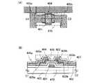
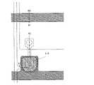
図1(A)は半導体装置の有する薄膜トランジスタ470の平面図であり、図1(B)は
図1(A)の線C1-C2における断面図である。薄膜トランジスタ470は逆スタガ型
の薄膜トランジスタであり、絶縁表面を有する基板である基板400上に、ゲート電極層
401、ゲート絶縁層402、半導体層403、バッファ層404、ソース電極層又はド
レイン電極層405a、405bを含む。また、薄膜トランジスタ470を覆い、バッフ
ァ層404に接する絶縁膜407が設けられている。1 (A) is a plan view of a
バッファ層404は、ソース電極層又はドレイン電極層405a、405bと接する低抵
抗領域である第1の領域409a、409b、及び半導体層403のチャネル形成領域と
接する高抵抗領域である第2の領域408を有している。なお明細書の図面において、バ
ッファ層404、半導体層403の網掛けの領域を低抵抗領域である第1の領域409a
、409b、低抵抗領域435a、435bとして示す。The
, 409b,
バッファ層404は膜内に抵抗分布を有し、半導体層403のチャネル形成領域上に設け
られる第2の領域408の電気伝導度は半導体層403のチャネル形成領域の電気伝導度
より低く、ソース電極層又はドレイン電極層405a、405bと接する第1の領域40
9a、409bの電気伝導度は半導体層403のチャネル形成領域の電気伝導度より高い
。また、バッファ層404及び半導体層403は、ゲート絶縁層402よりも電気伝導度
が高い(抵抗が低い)。よって、電気伝導度は高い順から、バッファ層404の低抵抗領
域(第1の領域409a、409b)、半導体層403のチャネル形成領域、バッファ層
404の高抵抗領域(第2の領域408)、ゲート絶縁層402となる。The
The electrical conductivity of 9a and 409b is higher than the electrical conductivity of the channel forming region of the
チャネル形成領域と接する領域のバッファ層は高抵抗化領域であるので、薄膜トランジス
タの電気特性は安定化し、オフ電流の増加などを防止することができる。一方、ソース電
極層及びドレイン電極層と接する領域のバッファ層は低抵抗領域であるので、コンタクト
抵抗が低く、オン電流は高くすることができる。よって、電気特性が高く信頼性のよい薄
膜トランジスタを有する半導体装置とすることが可能となる。Since the buffer layer in the region in contact with the channel formation region is a high resistance region, the electrical characteristics of the thin film transistor can be stabilized and an increase in off-current can be prevented. On the other hand, since the buffer layer in the region in contact with the source electrode layer and the drain electrode layer is a low resistance region, the contact resistance is low and the on-current can be high. Therefore, it is possible to obtain a semiconductor device having a thin film transistor having high electrical characteristics and high reliability.
バッファ層404は、チタン、モリブデン、又はマンガンを含む酸化物半導体層を用いる
ことができる。酸化物半導体層にチタン、モリブデン、又はマンガンの金属元素を含ませ
ると、酸化物半導体層は高抵抗化する。As the
バッファ層404の例として、In-Ga-Zn-O系酸化物半導体にチタン(Ti)、
又はモリブデン(Mo)を含ませた構造の電子状態について計算を行った。計算方法を以
下に示す。As an example of the
Alternatively, the electronic state of the structure containing molybdenum (Mo) was calculated. The calculation method is shown below.
Tiを含むIn-Ga-Zn-O系酸化物半導体構造、Moを含むIn-Ga-Zn-O
系酸化物半導体構造ともに密度は、非晶質In-Ga-Zn-O系酸化物半導体の実験値
5.9g/cm3に固定した。これらの2つの構造に対して、下記計算条件で計算を行っ
た。なお、古典分子動力学(MD)計算は富士通株式会社製の計算ソフトMateria
ls Explorer 5.0を用い、第一原理計算はaccelrys社製の第一原
理計算ソフトCASTEPを用いた。In-Ga-Zn-O oxide semiconductor structure containing Ti, In-Ga-Zn-O containing Mo
The density of both the oxide semiconductor structures was fixed at the experimental value of 5.9 g / cm3 for the amorphous In-Ga-Zn-O oxide semiconductor. Calculations were performed for these two structures under the following calculation conditions. The classical molecular dynamics (MD) calculation is performed by Fujitsu Limited's calculation software Materia.
ls Explorer 5.0 was used, and first-principles calculation software CASTEP manufactured by accelrys was used for the first-principles calculation.
最初に、古典分子動力学(MD)計算と第一原理計算により作製したIn-Ga-Zn-
O系酸化物半導体にTiまたはMoを含ませた。次に、第一原理計算で温度3000Kよ
り、1500K、300Kと温度を降温させながら、粒子数(N)、体積(V)、温度(
T)が一定の条件(アンサンブルNVT)で、時間刻み幅1fsec、各温度でのステッ
プ数2000step、電子のカットオフエネルギー260eV、逆格子のメッシュ(k
点)1×1×1で計算し、最後に第一原理計算で電子のカットオフエネルギー420eV
、逆格子のメッシュ(k点)2×2×2で構造最適化した。First, In-Ga-Zn- produced by classical molecular dynamics (MD) calculation and first-principles calculation.
Ti or Mo was impregnated in the O-based oxide semiconductor. Next, while lowering the temperature from 3000K to 1500K and 300K in the first principle calculation, the number of particles (N), volume (V), and temperature (
Under certain conditions (T) (ensemble NVT), the time step width is 1 fsec, the number of steps at each temperature is 2000 steps, the cutoff energy of electrons is 260 eV, and the mesh of the reciprocal lattice (k).
Point) Calculate with 1x1x1, and finally with first-principles calculation, electron cutoff energy 420eV
, The structure was optimized with a reciprocal lattice mesh (k points) 2 × 2 × 2.
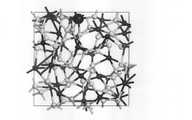
計算により得られたTi、またはMoを含むIn-Ga-Zn-O系酸化物半導体構造の
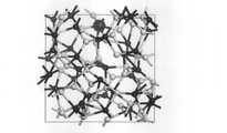
構造を図28及び図29に示す。黒丸が金属原子、白丸が酸素原子を表す。大きな黒丸が
Ti又はMoである。原子数は、図28のTiを含むIn-Ga-Zn-O系酸化物半導
体構造において、In、Ga、Znがそれぞれ12個、Oが50個、Tiが1個であり、
図29のMoを含むIn-Ga-Zn-O系酸化物半導体構造において、In、Ga、Z
nがそれぞれ12個、Oが51個、Moが1個である。The structure of the In—Ga—Zn—O oxide semiconductor structure containing Ti or Mo obtained by calculation is shown in FIGS. 28 and 29. Black circles represent metal atoms and white circles represent oxygen atoms. Large black circles are Ti or Mo. In the In—Ga—Zn—O oxide semiconductor structure containing Ti in FIG. 28, the number of atoms is 12 for In, Ga, and Zn, 50 for O, and 1 for Ti, respectively.
In-Ga-Zn-O-based oxide semiconductor structure containing Mo in FIG. 29, In, Ga, Z
There are 12 n, 51 O, and 1 Mo, respectively.
図28及び図29のTiを含むIn-Ga-Zn-O系酸化物半導体構造及びMoを含む
In-Ga-Zn-O系酸化物半導体構造に対して、第一原理計算で電子のカットオフエ
ネルギー420eV、逆格子のメッシュ(k点)が3×3×3の条件で、電子の状態密度
を計算した。Electron cutoff in the first-principles calculation for the In-Ga-Zn-O-based oxide semiconductor structure containing Ti and the In-Ga-Zn-O-based oxide semiconductor structure containing Mo in FIGS. 28 and 29. The density of states of electrons was calculated under the condition that the energy was 420 eV and the mesh (k point) of the reciprocal lattice was 3 × 3 × 3.
図30の(a)にIn-Ga-Zn-O系酸化物半導体構造、(b)にTiを含むIn-
Ga-Zn-O系酸化物半導体構造、(c)にMoを含むIn-Ga-Zn-O系酸化物
半導体構造それぞれにおける全体の状態密度を示す。図30(a)(b)(c)は、フェ
ルミエネルギーを横軸の原点に取っている。図30の(a)のIn-Ga-Zn-O系酸
化物半導体構造、(b)のTiを含むIn-Ga-Zn-O系酸化物半導体構造、(c)
のMoを含むIn-Ga-Zn-O系酸化物半導体構造全てにおいてバンドギャップがあ
り、価電子帯上端、伝導帯下端が図中に示すように位置づけられる。フェルミエネルギー
は価電子帯上端にある。In FIG. 30 (a) is an In—Ga—Zn—O oxide semiconductor structure, and (b) is In—containing Ti.
The overall density of states of each of the Ga—Zn—O oxide semiconductor structure and the In—Ga—Zn—O oxide semiconductor structure containing Mo in (c) is shown. In FIGS. 30 (a), (b) and (c), the Fermi energy is taken as the origin on the horizontal axis. (A) In—Ga—Zn—O-based oxide semiconductor structure of FIG. 30, (b) In—Ga—Zn—O-based oxide semiconductor structure containing Ti, (c).
There is a band gap in all the In-Ga-Zn-O oxide semiconductor structures including Mo, and the upper end of the valence band and the lower end of the conduction band are positioned as shown in the figure. Fermi energy is at the top of the valence band.
図31(a)、(b)、(c)にTiを含むIn-Ga-Zn-O系酸化物半導体構造の
(a)In、(b)Ga、(c)Znの1原子当たりの部分状態密度、図32(a)、(
b)、(c)にMoを含むIn-Ga-Zn-O系酸化物半導体構造の(a)In、(b
)Ga、(c)Znの1原子当たりの部分状態密度をそれぞれ示す。これらはそれぞれ系
内に12原子あるが、その平均を取った。図31(a)、(b)、(c)及び図32(a
)、(b)、(c)の結果を見ると、n型キャリアが入る伝導帯下端近傍の準位は、主に
In、Ga、Znのs軌道で形成されていることがわかる。31 (a), (b), (c) is a portion of (a) In, (b) Ga, (c) Zn of an In—Ga—Zn—O-based oxide semiconductor structure containing Ti per atom. Density of states, FIG. 32 (a), (
b) In-Ga-Zn-O oxide semiconductor structure containing Mo in (c) (a) In, (b)
) Ga and (c) Zn show the partial density of states per atom, respectively. Each of these has 12 atoms in the system, and the average is taken. 31 (a), (b), (c) and 32 (a).
), (B), and (c), it can be seen that the level near the lower end of the conduction band in which the n-type carrier enters is mainly formed by the s orbitals of In, Ga, and Zn.
一方、図31(d)にTiを含むIn-Ga-Zn-O系酸化物半導体構造のTi、図3
2(d)にMoを含むIn-Ga-Zn-O系酸化物半導体構造のMoの部分状態密度を
それぞれ示す。図31(d)及び図32(d)の結果を見ると、TiとMoの両方とも伝
導帯下端の準位に寄与しているが、絶対値はIn、Ga、Znよりも小さいことがわかる
。さらに最も寄与しているのはs軌道ではなく、d軌道である。これらのことから次の2
つの結論が導ける。第一に、TiやMoは伝導帯の下端の準位に寄与し難い。第二に、T
iやMoの濃度を上げると、伝導体下端の準位がIn、Ga、Znのs軌道よりもTiや
Moのd軌道によって構成されるようになる。d軌道はs軌道よりも異方性が強く、アモ
ルファス構造ではn型キャリアを伝導し難く、移動度は低下する。On the other hand, FIG. 31 (d) shows Ti of an In—Ga—Zn—O oxide semiconductor structure containing Ti, FIG. 3
2 (d) shows the partial density of states of Mo in the In—Ga—Zn—O oxide semiconductor structure containing Mo. Looking at the results of FIGS. 31 (d) and 32 (d), it can be seen that both Ti and Mo contribute to the level at the lower end of the conduction band, but the absolute value is smaller than In, Ga, and Zn. .. Furthermore, it is the d-orbital, not the s-orbital, that contributes most. From these things, the following 2
One conclusion can be drawn. First, Ti and Mo are unlikely to contribute to the lower level of the conduction band. Second, T
When the concentration of i and Mo is increased, the level at the lower end of the conductor is composed of the d orbitals of Ti and Mo rather than the s orbitals of In, Ga and Zn. The d-orbital has stronger anisotropy than the s-orbital, and it is difficult to conduct the n-type carrier in the amorphous structure, and the mobility is lowered.
以上の事から、TiやMoをIn-Ga-Zn-O系酸化物半導体に含ませると、高濃度
になるに伴いn型キャリアを流し難い、電気伝導度の小さい膜になる事がわかる。よって
、d軌道やf軌道が空になっている遷移金属元素であるTiやMoを、酸化物半導体層へ
含ませることによって、電気伝導度を小さく(高抵抗化)することができる。From the above, it can be seen that when Ti or Mo is contained in an In-Ga-Zn-O-based oxide semiconductor, a film having low electrical conductivity is formed in which it is difficult for n-type carriers to flow as the concentration increases. Therefore, by including Ti and Mo, which are transition metal elements whose d-orbital and f-orbital are empty, in the oxide semiconductor layer, the electric conductivity can be reduced (high resistance).
なお、ソース電極層又はドレイン電極層405a、405bに、酸素親和性の高い金属を
含有する材料を用いていることが好ましい。また、上記酸素親和性の高い金属は、チタン
、アルミニウム、マンガン、マグネシウム、ジルコニウム、ベリリウム、トリウムのいず
れか一または複数から選択された材料であることが好ましい。It is preferable to use a material containing a metal having a high oxygen affinity for the source electrode layer or the
バッファ層404に接するソース電極層又はドレイン電極層405a、405bは、酸素
親和性の高い金属を用いたものとすることが好ましい。酸素親和性の高い金属としては、
例えば、チタン、アルミニウム、マンガン、マグネシウム、ジルコニウム、ベリリウム、
トリウムなどの、亜鉛と比較して標準電極電位が小さい金属が挙げられる。また、銅など
を用いても良い。このように、酸素親和性の高い金属と、酸化物半導体層とが接する構成
として熱処理等を行うことにより、酸化物半導体層であるバッファ層404のソース電極
層又はドレイン電極層405a、405bと接する領域の酸素の組成比は、他の領域のそ
れと比較して小さくなる。該低酸素領域においては導電性が向上する傾向にあるから、低
抵抗領域となる。なお、酸素親和性の高い金属は上記材料に限定されない。It is preferable that the source electrode layer or the
For example, titanium, aluminum, manganese, magnesium, zirconium, beryllium,
Examples include metals such as thorium, which have a smaller standard electrode potential than zinc. Further, copper or the like may be used. As described above, by performing heat treatment or the like as a structure in which the metal having high oxygen affinity and the oxide semiconductor layer are in contact with each other, the metal is in contact with the source electrode layer or the
上記現象は、酸素親和性の高い金属が酸化物半導体層から酸素を引き抜くことに起因する
ものであるから、電極層の酸化物半導体層と接する領域の酸素の組成比は、他の領域のそ
れと比較して大きくなると考えられる(つまり、該領域において、電極層は酸化される)
。これを考慮するならば、酸化物半導体層と接する領域の電極層において形成される金属
酸化物は、導電性を有していることが好ましい。例えば、酸素親和性の高い金属としてチ
タンを用いる場合であれば、一酸化物に近い組成比(例えば、TiOxとした場合に0.
5<x<1.5程度)の酸化物が形成される条件で各種処理を行えばよい。これは、チタ
ンの一酸化物は導電性を有するが、チタンの二酸化物は絶縁性を有するためである。Since the above phenomenon is caused by the extraction of oxygen from the oxide semiconductor layer by a metal having a high oxygen affinity, the composition ratio of oxygen in the region of the electrode layer in contact with the oxide semiconductor layer is that of that of the other regions. It is considered to be larger in comparison (that is, the electrode layer is oxidized in the region).
.. Considering this, it is preferable that the metal oxide formed in the electrode layer in the region in contact with the oxide semiconductor layer has conductivity. For example, when titanium is used as a metal having a high oxygen affinity, the composition ratio is close to that of a monooxide (for example, when TiOx is used, the composition ratio is 0.
Various treatments may be performed under the condition that an oxide of 5 <x <1.5) is formed. This is because one oxide of titanium has conductivity, but the dioxide of titanium has insulating properties.
ここで、酸素親和性の高い金属を電極層として用いる場合の効果について、計算機シミュ
レーションに基づいて説明する。ここでは、酸素親和性の高い金属としてチタンを用い、
酸化物半導体層として、In-Ga-Zn-O系の酸化物半導体材料を用いる場合につい
て計算を行っているが、開示する発明の一態様はこれに限定されない。なお、計算におい
て、In-Ga-Zn-O系の酸化物半導体材料の組成はIn:Ga:Zn:O=1:1
:1:4とした。Here, the effect of using a metal having a high oxygen affinity as the electrode layer will be described based on a computer simulation. Here, titanium is used as a metal with high oxygen affinity.
Although the calculation is performed for the case where an In—Ga—Zn—O-based oxide semiconductor material is used as the oxide semiconductor layer, one aspect of the disclosed invention is not limited to this. In the calculation, the composition of the In—Ga—Zn—O-based oxide semiconductor material is In: Ga: Zn: O = 1: 1.
It was set to 1: 4.
はじめに、非晶質状態の酸化物半導体から酸素が失われることによる効果を検証した。First, the effect of oxygen loss from the amorphous oxide semiconductor was examined.
まず、古典MD(分子動力学)計算を用いたmelt-quench法により、In-G
a-Zn-O系酸化物半導体の非晶質構造を用意した。ここでは、総原子数が84個、密
度が5.9g/cm3の構造について計算を行っている。金属-酸素間および酸素-酸素
間についてはBorn-Mayer-Huggins型のポテンシャルを、金属-金属間
についてはLennard-Jones型のポテンシャルを用い、NVTアンサンブルで
計算を行った。計算プログラムとしては、Materials Explorerを用い
た。First, In-G by the melt-quench method using classical MD (molecular dynamics) calculation.
An amorphous structure of an a—Zn—O oxide semiconductor was prepared. Here, the calculation is performed for a structure having a total number of atoms of 84 and a density of 5.9 g / cm3 . The NVT ensemble was calculated using the Born-Mayer-Huggins type potential for the metal-oxygen and oxygen-oxygen, and the Lennard-Jones type potential for the metal-metal. As a calculation program, Material Explorer was used.
その後、上記古典MD計算により得られた構造に対して、密度汎関数理論(DFT)に基
づく平面波-擬ポテンシャル法を用いた第一原理計算(量子MD計算)により、構造を最
適化し、状態密度を求めた。また、任意の酸素原子を一つ取り除いた構造に対しても構造
最適化を行い、状態密度を計算した。計算プログラムとしてはCASTEPを、交換相関
汎関数としてはGGA-PBEを用いた。After that, for the structure obtained by the classical MD calculation, the structure is optimized by the first-principles calculation (quantum MD calculation) using the plane wave-pseudopotential method based on the density functional theory (DFT), and the density of states. Asked. In addition, the structure was optimized for the structure from which one arbitrary oxygen atom was removed, and the density of states was calculated. CASTEP was used as the calculation program, and GGA-PBE was used as the exchange correlation functional.
図33に、上記計算結果により得られた構造の状態密度を示す。図33(A)は、酸素欠
損のない構造の状態密度であり、図33(B)は、酸素欠損がある構造の状態密度である
。ここで、0(eV)はフェルミ準位に対応するエネルギーを表している。図33(A)
および図33(B)より、酸素欠損がない構造では、フェルミ準位は価電子帯の上端に存
在するのに対して、酸素欠損がある構造では、フェルミ準位は伝導帯中に存在することが
分かる。酸素欠損がある構造ではフェルミ準位が伝導帯中に存在するため、伝導に寄与す
る電子数が増加し、抵抗が低い(導電率の高い)構造が得られる。FIG. 33 shows the density of states of the structure obtained by the above calculation result. FIG. 33 (A) is the density of states of the structure without oxygen deficiency, and FIG. 33 (B) is the density of states of the structure without oxygen deficiency. Here, 0 (eV) represents the energy corresponding to the Fermi level. FIG. 33 (A)
And from FIG. 33 (B), in the structure without oxygen deficiency, the Fermi level exists at the upper end of the valence band, whereas in the structure with oxygen deficiency, the Fermi level exists in the conduction band. I understand. In a structure with oxygen deficiency, the Fermi level exists in the conduction band, so the number of electrons contributing to conduction increases, and a structure with low resistance (high conductivity) can be obtained.
次に、電極層として酸素親和性の高い金属を用いることにより、非晶質状態の酸化物半導
体から酸素親和性の高い金属へと酸素が移動する様子を確認した。Next, it was confirmed that oxygen was transferred from the amorphous oxide semiconductor to the metal having high oxygen affinity by using a metal having high oxygen affinity as the electrode layer.
ここでは、前述の第一原理計算によって得られたIn-Ga-Zn-O系の非晶質構造上
にチタン結晶を積層し、当該構造に対してNVTアンサンブルで量子MD計算を行った。
計算プログラムとしてはCASTEPを、交換相関汎関数としてはGGA-PBEを用い
た。また、温度条件は623K(350℃)とした。Here, titanium crystals were laminated on the In—Ga—Zn—O-based amorphous structure obtained by the above-mentioned first-principles calculation, and quantum MD calculation was performed on the structure with an NVT ensemble.
CASTEP was used as the calculation program, and GGA-PBE was used as the exchange correlation functional. The temperature condition was 623K (350 ° C.).
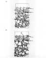
図34に量子MD計算前後の構造を示す。図34(A)は、量子MD計算前の構造であり
、図34(B)は、量子MD計算後の構造である。量子MD計算後の構造では、量子MD
計算前と比較して、チタンと結合した酸素の数が増加している。該構造変化は、非晶質状
態の酸化物半導体層から酸素親和性の高い金属層へと酸素原子が移動することを示唆して
いる。FIG. 34 shows the structure before and after the quantum MD calculation. FIG. 34 (A) is a structure before the quantum MD calculation, and FIG. 34 (B) is a structure after the quantum MD calculation. In the structure after quantum MD calculation, quantum MD
Compared to before the calculation, the number of oxygen bound to titanium has increased. The structural change suggests that oxygen atoms move from the amorphous oxide semiconductor layer to the metal layer having high oxygen affinity.
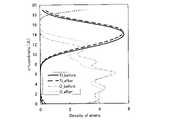
図35に量子MD計算前後における、チタンおよび酸素の密度を示す。各曲線はそれぞれ
、量子MD計算前のチタンの密度(Ti_before)、量子MD計算後のチタンの密
度(Ti_after)、量子MD計算前の酸素の密度(O_before)、量子MD
計算後の酸素の密度(O_after)を表している。図35からも、酸素親和性の高い
金属へと酸素原子が移動することが分かる。FIG. 35 shows the densities of titanium and oxygen before and after the quantum MD calculation. Each curve shows the titanium density before the quantum MD calculation (Ti_before), the titanium density after the quantum MD calculation (Ti_after), the oxygen density before the quantum MD calculation (O_before), and the quantum MD.
It represents the calculated oxygen density (O_after). From FIG. 35, it can be seen that the oxygen atom moves to the metal having a high oxygen affinity.
このように、酸化物半導体層と、酸素親和性の高い金属層とを接触させて熱処理を行うこ
とにより、酸化物半導体層から金属層へと酸素原子が移動し、界面付近においてキャリア
密度が増加することが確認された。これは、界面付近において低抵抗な領域が形成される
ことを示唆するものであり、半導体層と電極層とのコンタクト抵抗低減の効果をもたらす
といえる。In this way, by contacting the oxide semiconductor layer with the metal layer having high oxygen affinity and performing heat treatment, oxygen atoms move from the oxide semiconductor layer to the metal layer, and the carrier density increases near the interface. It was confirmed that This suggests that a low resistance region is formed near the interface, and can be said to bring about the effect of reducing the contact resistance between the semiconductor layer and the electrode layer.
チャネル形成領域を含む半導体層403としては、半導体特性を有する酸化物材料を用い
ればよい。例えば、InMO3(ZnO)m(m>0)で表記される構造の酸化物半導体
を用いることができ、特に、In-Ga-Zn-O系酸化物半導体を用いるのが好ましい
。なお、Mは、ガリウム(Ga)、鉄(Fe)、ニッケル(Ni)、マンガン(Mn)及
びコバルト(Co)から選ばれた一の金属元素又は複数の金属元素を示す。例えばMとし
て、Gaの場合があることの他、GaとNi又はGaとFeなど、Ga以外の上記金属元
素が含まれる場合がある。また、上記酸化物半導体において、Mとして含まれる金属元素
の他に、不純物元素としてFe、Niその他の遷移金属元素、又は該遷移金属の酸化物が
含まれているものがある。本明細書においては、InMO3(ZnO)m(m>0)で表
記される構造の酸化物半導体のうち、Mとして少なくともGaを含む構造の酸化物半導体
をIn-Ga-Zn-O系酸化物半導体と呼び、該薄膜をIn-Ga-Zn-O系非単結
晶膜とも呼ぶ。As the
また、酸化物半導体層に適用する酸化物半導体として上記の他にも、In-Sn-Zn-
O系、In-Al-Zn-O系、Sn-Ga-Zn-O系、Al-Ga-Zn-O系、S
n-Al-Zn-O系、In-Zn-O系、Sn-Zn-O系、Al-Zn-O系、In
-O系、Sn-O系、Zn-O系の酸化物半導体を適用することができる。In addition to the above, In-Sn-Zn- is also used as an oxide semiconductor applied to the oxide semiconductor layer.
O system, In-Al-Zn-O system, Sn-Ga-Zn-O system, Al-Ga-Zn-O system, S
n-Al-Zn-O system, In-Zn-O system, Sn-Zn-O system, Al-Zn-O system, In
-O-based, Sn—O-based, and Zn—O-based oxide semiconductors can be applied.
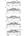
図2(A)乃至(E)は薄膜トランジスタ470の作製工程を示す断面図に相当する。FIGS. 2A to 2E correspond to cross-sectional views showing a manufacturing process of the
図2(A)において、絶縁表面を有する基板である基板400上にゲート電極層401を
設ける。下地膜となる絶縁膜を基板400とゲート電極層401の間に設けてもよい。下
地膜は、基板400からの不純物元素の拡散を防止する機能があり、窒化珪素膜、酸化珪
素膜、窒化酸化珪素膜、又は酸化窒化珪素膜から選ばれた一又は複数の膜による積層構造
により形成することができる。ゲート電極層401の材料は、モリブデン、チタン、クロ
ム、タンタル、タングステン、アルミニウム、銅、ネオジム、スカンジウム等の金属材料
又はこれらを主成分とする合金材料を用いて、単層で又は積層して形成することができる
。In FIG. 2A, the
例えば、ゲート電極層401の2層の積層構造としては、アルミニウム層上にモリブデン
層が積層された2層の積層構造、または銅層上にモリブデン層を積層した二層構造、また
は銅層上に窒化チタン層若しくは窒化タンタル層を積層した二層構造、窒化チタン層とモ
リブデン層とを積層した二層構造とすることが好ましい。3層の積層構造としては、タン
グステン層または窒化タングステン層と、アルミニウムとシリコンの合金またはアルミニ
ウムとチタンの合金と、窒化チタンまたはチタン層とを積層した構造とすることが好まし
い。For example, the two-layer laminated structure of the
ゲート電極層401上にゲート絶縁層402を形成する。A
ゲート絶縁層402は、プラズマCVD法又はスパッタリング法等を用いて、酸化シリコ
ン層、窒化シリコン層、酸化窒化シリコン層又は窒化酸化シリコン層を単層で又は積層し
て形成することができる。また、ゲート絶縁層402として、有機シランガスを用いたC
VD法により酸化シリコン層を形成することも可能である。有機シランガスとしては、珪
酸エチル(TEOS:化学式Si(OC2H5)4)、テトラメチルシラン(TMS:化
学式Si(CH3)4)、テトラメチルシクロテトラシロキサン(TMCTS)、オクタ
メチルシクロテトラシロキサン(OMCTS)、ヘキサメチルジシラザン(HMDS)、
トリエトキシシラン(SiH(OC2H5)3)、トリスジメチルアミノシラン(SiH
(N(CH3)2)3)等のシリコン含有化合物を用いることができる。The
It is also possible to form a silicon oxide layer by the VD method. Examples of the organic silane gas include ethyl silicate (TEOS: chemical formula Si (OC2 H5 )4 ), tetramethylsilane (TMS: chemical formula Si (CH3 )4 ), tetramethylcyclotetrasiloxane (TMCTS), and octamethylcyclotetrasiloxane. (OMCTS), Hexamethyldisilazane (HMDS),
Triethoxysilane (SiH (OC2H5 )3 ), tridimethylaminosilane (SiH)
Silicon-containing compounds such as (N (CH3 )2 )3 ) can be used.
ゲート絶縁層402上に、第1の酸化物半導体膜433、第2の酸化物半導体膜434を
順に積層する(図2(A)参照。)。The first
なお、第1の酸化物半導体膜433をスパッタ法により成膜する前に、アルゴンガスを導
入してプラズマを発生させる逆スパッタを行い、ゲート絶縁層402の表面に付着してい
るゴミを除去することが好ましい。逆スパッタとは、ターゲット側に電圧を印加せずに、
アルゴン雰囲気下で基板側にRF電源を用いて電圧を印加して基板にプラズマを形成して
表面を改質する方法である。Before forming the first
This is a method of modifying the surface by forming plasma on the substrate by applying a voltage to the substrate side using an RF power supply in an argon atmosphere.
なお、アルゴン雰囲気に代えて窒素、ヘリウムなどを用いてもよい。また、アルゴン雰囲
気に酸素、N2Oなどを加えた雰囲気で行ってもよい。また、アルゴン雰囲気にCl2、
CF4などを加えた雰囲気で行ってもよい。In addition, nitrogen, helium or the like may be used instead of the argon atmosphere. Further, it may be performed in an atmosphere in which oxygen,N2O , or the like is added to an argon atmosphere. Also, in the argon atmosphere, Cl2 ,
It may be performed in an atmosphere in which CF4 or the like is added.
第1の酸化物半導体膜433としてIn-Ga-Zn-O系非単結晶膜を用いる。第1の
酸化物半導体膜433は、In-Ga-Zn-O系酸化物半導体ターゲットを用いてスパ
ッタ法により成膜する。An In—Ga—Zn—O-based non-single crystal film is used as the first
第2の酸化物半導体膜434としてチタンを含むIn-Ga-Zn-O系非単結晶膜を用
いる。第2の酸化物半導体膜434は、酸化チタンを含むIn-Ga-Zn-Oターゲッ
トを用いてスパッタ法により成膜する。As the second
ゲート絶縁層402、第1の酸化物半導体膜433、第2の酸化物半導体膜434を大気
に触れさせることなく連続的に形成してもよい。大気に触れさせることなく連続成膜する
ことで、大気成分や大気中に浮遊する不純物元素に汚染されることなく各積層界面を形成
することができるので、薄膜トランジスタ特性のばらつきを低減することができる。The
第1の酸化物半導体膜433、第2の酸化物半導体膜434をフォトリソグラフィ工程に
より島状の酸化物半導体層である半導体層403、酸化物半導体層431に加工する。The first
ゲート絶縁層402、半導体層403、及び酸化物半導体層431上に導電膜432を形
成する(図2(B)参照。)。A
導電膜432の材料としては、酸素親和性の高い金属であるチタン膜を用いる。また、チ
タン膜上にAl、Cr、Ta、Mo、Wから選ばれた元素、または上述した元素を成分と
する合金か、上述した元素を組み合わせた合金膜などを積層してもよい。As the material of the
酸化物半導体層431、導電膜432をエッチング工程によりエッチングし、バッファ層
404、ソース電極層又はドレイン電極層405a、405bを形成する(図2(C)参
照。)。なお、バッファ層404は一部のみがエッチングされ、溝部(凹部)を有するバ
ッファ層404となる。The
次に、酸化物半導体層であるバッファ層404及びソース電極層又はドレイン電極層40
5a、405bに加熱処理を行う。加熱処理により酸化物半導体層から金属層へと酸素原
子が移動するので、ソース電極層又はドレイン電極層405a、405bと接する第1の
領域409a、409bは低抵抗化する。一方半導体層403のチャネル形成領域と接す
る第2の領域408は高抵抗なままである。よってバッファ層404に低抵抗領域である
第1の領域409a、409b及び高抵抗領域である第2の領域408が形成される(図
2(D)参照。)。また、この加熱処理により、半導体層403のソース電極層又はドレ
イン電極層405a、405bと接する領域も、同様に酸化物半導体層から金属層へと酸
素原子が移動して、低抵抗領域435a、435bが形成される。Next, the
Heat treatment is performed on 5a and 405b. Since oxygen atoms move from the oxide semiconductor layer to the metal layer by the heat treatment, the resistance of the
加熱処理は、200℃~600℃、代表的には300℃~500℃で行うと良い。例えば
、窒素雰囲気下で350℃、1時間の熱処理を行う。The heat treatment may be performed at 200 ° C. to 600 ° C., typically 300 ° C. to 500 ° C. For example, heat treatment is performed at 350 ° C. for 1 hour in a nitrogen atmosphere.
以上の工程で、図2(E)に示す逆スタガ型の薄膜トランジスタ470を作製することが
できる。また、薄膜トランジスタ470を覆い、バッファ層404に接する絶縁膜407
を形成している。Through the above steps, the inverted stagger type
Is forming.
チャネル形成領域と接する領域のバッファ層は高抵抗化領域であるので、薄膜トランジス
タの電気特性は安定化し、オフ電流の増加などを防止することができる。一方、ソース電
極層及びドレイン電極層と接する領域のバッファ層は低抵抗領域であるので、コンタクト
抵抗が低く、オン電流は高くすることができる。よって、電気特性が高く信頼性のよい薄
膜トランジスタを有する半導体装置とすることが可能となる。Since the buffer layer in the region in contact with the channel formation region is a high resistance region, the electrical characteristics of the thin film transistor can be stabilized and an increase in off-current can be prevented. On the other hand, since the buffer layer in the region in contact with the source electrode layer and the drain electrode layer is a low resistance region, the contact resistance is low and the on-current can be high. Therefore, it is possible to obtain a semiconductor device having a thin film transistor having high electrical characteristics and high reliability.
(実施の形態2)
ここでは、実施の形態1において、チャネル形成領域を有する酸化物半導体層とバッファ
層とが異なるエッチング工程で加工された薄膜トランジスタを有する半導体装置の例を図
3及び図4に示す。従って、他は実施の形態1と同様に行うことができ、実施の形態1と
同一部分又は同様な機能を有する部分、及び工程の繰り返しの説明は省略する。(Embodiment 2)
Here, FIGS. 3 and 4 show an example of a semiconductor device having a thin film transistor in which the oxide semiconductor layer having a channel forming region and the buffer layer are processed in different etching steps in the first embodiment. Therefore, other parts can be performed in the same manner as in the first embodiment, and the description of the part having the same or the same function as that of the first embodiment and the repetition of the process will be omitted.
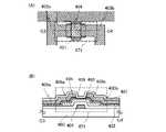
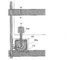
図3(A)は半導体装置の有する薄膜トランジスタ471の平面図であり、図3(B)は
図3(A)の線C3-C4における断面図である。薄膜トランジスタ471は逆スタガ型
の薄膜トランジスタであり、絶縁表面を有する基板である基板400上に、ゲート電極層
401、ゲート絶縁層402、半導体層403、バッファ層404、ソース電極層又はド
レイン電極層405a、405bを含む。また、薄膜トランジスタ471を覆い、バッフ
ァ層404に接する絶縁膜407が設けられている。3A is a plan view of the
バッファ層404は、ソース電極層又はドレイン電極層405a、405bと接する低抵
抗領域である第1の領域409a、409b、及び半導体層403のチャネル形成領域と
接する高抵抗領域である第2の領域408を有している。The
薄膜トランジスタ471においては、バッファ層404は、半導体層403の端部を覆っ
てソース電極層又はドレイン電極層405a、405bの下に延在して形成されている。In the
図4(A)乃至(E)は薄膜トランジスタ471の作製工程を示す断面図に相当する。FIGS. 4A to 4E correspond to cross-sectional views showing a manufacturing process of the
絶縁表面を有する基板である基板400上にゲート電極層401を設け、ゲート電極層4
01上にゲート絶縁層402を形成する。The
A
ゲート絶縁層402上に、酸化物半導体膜を形成し、島状にエッチング加工して半導体層
403を形成する(図4(A)参照。)。An oxide semiconductor film is formed on the
島状に加工された半導体層403上を覆うように酸化物半導体膜436を形成し、酸化物
半導体膜436上に導電膜432を積層する(図4(B)参照。)。酸化物半導体膜43
6は、実施の形態1における第2の酸化物半導体膜434と同様の膜であり、チタンを含
むIn-Ga-Zn-O系非単結晶膜を用いる。酸化物半導体膜436は、酸化チタンを
含むIn-Ga-Zn-Oターゲットを用いてスパッタ法により成膜する。The oxide semiconductor film 436 is formed so as to cover the island-shaped
導電膜432の材料としては、酸素親和性の高い金属であるチタン膜を用いる。As the material of the
酸化物半導体膜436、導電膜432をエッチング工程によりエッチングし、バッファ層
404、ソース電極層又はドレイン電極層405a、405bを形成する(図4(C)参
照。)。なお、バッファ層404は一部のみがエッチングされ、溝部(凹部)を有するバ
ッファ層404となる。The oxide semiconductor film 436 and the
次に、酸化物半導体層であるバッファ層404及びソース電極層又はドレイン電極層40
5a、405bに加熱処理を行う。加熱処理により酸化物半導体層から金属層へと酸素原
子が移動するので、ソース電極層又はドレイン電極層405a、405bと接する第1の
領域409a、409bは低抵抗化する。一方半導体層403のチャネル形成領域と接す
る第2の領域408は高抵抗なままである。よってバッファ層404に低抵抗領域である
第1の領域409a、409b及び高抵抗領域である第2の領域408が形成される(図
4(D)参照。)。Next, the
Heat treatment is performed on 5a and 405b. Since oxygen atoms move from the oxide semiconductor layer to the metal layer by the heat treatment, the resistance of the
加熱処理は、200℃~600℃、代表的には300℃~500℃で行うと良い。例えば
、窒素雰囲気下で350℃、1時間の熱処理を行う。The heat treatment may be performed at 200 ° C. to 600 ° C., typically 300 ° C. to 500 ° C. For example, heat treatment is performed at 350 ° C. for 1 hour in a nitrogen atmosphere.
以上の工程で、図4(E)に示す逆スタガ型の薄膜トランジスタ471を作製することが
できる。また、薄膜トランジスタ471を覆い、バッファ層404に接する絶縁膜407
を形成している。Through the above steps, the inverted stagger type
Is forming.
このように、薄膜トランジスタの作製工程において、エッチング加工の工程順を変化させ
ることで、形状の異なる薄膜トランジスタを種々作製することができる。As described above, in the process of manufacturing the thin film transistor, various thin film transistors having different shapes can be manufactured by changing the step order of the etching process.
チャネル形成領域と接する領域のバッファ層は高抵抗化領域であるので、薄膜トランジス
タの電気特性は安定化し、オフ電流の増加などを防止することができる。一方、ソース電
極層及びドレイン電極層と接する領域のバッファ層は低抵抗領域であるので、コンタクト
抵抗が低く、オン電流は高くすることができる。よって、電気特性が高く信頼性のよい薄
膜トランジスタを有する半導体装置とすることが可能となる。Since the buffer layer in the region in contact with the channel formation region is a high resistance region, the electrical characteristics of the thin film transistor can be stabilized and an increase in off-current can be prevented. On the other hand, since the buffer layer in the region in contact with the source electrode layer and the drain electrode layer is a low resistance region, the contact resistance is low and the on-current can be high. Therefore, it is possible to obtain a semiconductor device having a thin film transistor having high electrical characteristics and high reliability.
(実施の形態3)
半導体装置及び半導体装置の作製方法の他の例を図5及び図6を用いて説明する。本実施
の形態は、実施の形態1及び2において、バッファ層の材料及び作製方法が異なる例であ
る。従って、他は実施の形態1及び2と同様に行うことができ、実施の形態1及び2と同
一部分又は同様な機能を有する部分、及び工程の繰り返しの説明は省略する。(Embodiment 3)
Other examples of the semiconductor device and the method for manufacturing the semiconductor device will be described with reference to FIGS. 5 and 6. This embodiment is an example in which the material and the manufacturing method of the buffer layer are different between the first and second embodiments. Therefore, the other parts can be performed in the same manner as in the first and second embodiments, and the description of the same part as that of the first and second embodiments or the part having the same function and the repetition of the process will be omitted.
図5(A)は半導体装置の有する薄膜トランジスタ460の平面図であり、図5(B)は
図5(A)の線D1-D2における断面図である。薄膜トランジスタ460は逆スタガ型
の薄膜トランジスタであり、絶縁表面を有する基板である基板450上に、ゲート電極層
451、ゲート絶縁層452、半導体層453、バッファ層454、ソース電極層又はド
レイン電極層455a、455bを含む。また、薄膜トランジスタ460を覆い、バッフ
ァ層454に接する絶縁膜457が設けられている。5 (A) is a plan view of the
バッファ層454は、ソース電極層又はドレイン電極層455a、455bと接する低抵
抗領域である第1の領域459a、459b、及び半導体層453のチャネル形成領域と
接する高抵抗領域である第2の領域458を有している。The
バッファ層454は膜内に抵抗分布を有し、半導体層453のチャネル形成領域上に設け
られる第2の領域458の電気伝導度は半導体層453のチャネル形成領域の電気伝導度
より低く、ソース電極層又はドレイン電極層455a、455bと接する第1の領域45
9a、459bの電気伝導度は半導体層453のチャネル形成領域の電気伝導度より高い
。また、バッファ層454及び半導体層453は、ゲート絶縁層452よりも電気伝導度
が高い(抵抗が低い)。よって、電気伝導度は高い順から、バッファ層454の低抵抗領
域(第1の領域459a、459b)、半導体層453のチャネル形成領域、バッファ層
454の高抵抗領域(第2の領域458)、ゲート絶縁層452となる。The
The electrical conductivity of 9a and 459b is higher than the electrical conductivity of the channel forming region of the
バッファ層454は、低抵抗な第1の領域459a、459bを金属領域、及び高抵抗な
第2の領域458を金属酸化領域で構成されている膜である。このようなバッファ層45
4は、金属膜を形成後、その金属膜に選択的に酸化処理を行うことで形成することができ
る。The
No. 4 can be formed by forming a metal film and then selectively oxidizing the metal film.
図6(A)乃至(E)は薄膜トランジスタ460の作製工程を示す断面図を示す。6 (A) to 6 (E) are cross-sectional views showing a manufacturing process of the
基板450上にゲート電極層451を形成し、ゲート電極層451上にゲート絶縁層45
2を形成する。A
ゲート絶縁層452上に、酸化物半導体膜463を形成し、酸化物半導体膜463上に金
属膜464を順に積層する(図6(A)参照。)。An
酸化物半導体膜463としてIn-Ga-Zn-O系非単結晶膜を用いる。酸化物半導体
膜463は、In-Ga-Zn-O系酸化物半導体ターゲットを用いてスパッタ法により
成膜する。An In—Ga—Zn—O-based non-single crystal film is used as the
金属膜464は、高抵抗領域を形成するために作製工程において選択的に酸化処理が可能
な材料であればよく、タンタル(Ta)やアルミニウム(Al)を用いることができる。
金属膜464としてタンタル膜を形成する。The
A tantalum film is formed as a
酸化物半導体膜463、金属膜464をフォトリソグラフィ工程により島状の酸化物半導
体層である半導体層453、バッファ層454に加工する。The
ゲート絶縁層452、半導体層453、及びバッファ層454上に導電膜462を形成す
る(図6(B)参照。)。A
導電膜462をエッチング工程によりエッチングし、ソース電極層又はドレイン電極層4
55a、455bを形成する(図6(C)参照。)。The
It forms 55a and 455b (see FIG. 6C).
次に、バッファ層454に選択的に酸化処理を行う。酸化処理としては、プラズマ処理や
薬液による改質処理を行えばよい。バッファ層454のソース電極層又はドレイン電極層
455a、455bに覆われていない領域に酸化処理として酸素プラズマ処理を行い、高
抵抗な金属酸化領域を形成する。この金属酸化領域はバッファ層454において半導体層
453のチャネル形成領域と接する第2の領域458である。一方、ソース電極層又はド
レイン電極層455a、455bと接する第1の領域459a、459bは酸化処理され
ないので、低抵抗な金属領域のままである。よってバッファ層454に低抵抗領域である
第1の領域459a、459b及び高抵抗領域である第2の領域458が形成される(図
6(D)参照。)。Next, the
その後、200℃~600℃、代表的には300℃~500℃の熱処理を行うと良い。例
えば、窒素雰囲気下で350℃、1時間の熱処理を行う。この熱処理により半導体層45
3を構成するIn-Ga-Zn-O系酸化物半導体の原子レベルの再配列が行われる。こ
の熱処理(光アニール等も含む)は、半導体層453中におけるキャリアの移動を阻害す
る歪みを解放できる。なお、上記の熱処理を行うタイミングは、酸化物半導体膜463の
形成後であれば特に限定されない。After that, heat treatment at 200 ° C. to 600 ° C., typically 300 ° C. to 500 ° C. may be performed. For example, heat treatment is performed at 350 ° C. for 1 hour in a nitrogen atmosphere. By this heat treatment, the semiconductor layer 45
The atomic level rearrangement of the In—Ga—Zn—O oxide semiconductor constituting No. 3 is performed. This heat treatment (including photoannealing and the like) can release the strain that hinders the movement of carriers in the
また、ソース電極層又はドレイン電極層455a、455bに酸素親和性の高い金属であ
るチタン膜を用いるため、この加熱処理により、半導体層453のソース電極層又はドレ
イン電極層455a、455bと接する領域では、実施の形態1及び2と同様に酸化物半
導体層から金属層へと酸素原子が移動して、低抵抗領域465a、465bが形成される
。Further, since a titanium film which is a metal having high oxygen affinity is used for the source electrode layer or the
以上の工程で、図6(E)に示す半導体層453をチャネル形成領域とする逆スタガ型の
薄膜トランジスタ460を作製することができる。また、薄膜トランジスタ460を覆い
、バッファ層454に接する絶縁膜457を形成している。Through the above steps, an inverted staggered
チャネル形成領域と接する領域のバッファ層は高抵抗化領域であるので、薄膜トランジス
タの電気特性は安定化し、オフ電流の増加などを防止することができる。一方、ソース電
極層及びドレイン電極層と接する領域のバッファ層は低抵抗領域であるので、コンタクト
抵抗が低く、オン電流は高くすることができる。よって、電気特性が高く信頼性のよい薄
膜トランジスタを有する半導体装置とすることが可能となる。Since the buffer layer in the region in contact with the channel formation region is a high resistance region, the electrical characteristics of the thin film transistor can be stabilized and an increase in off-current can be prevented. On the other hand, since the buffer layer in the region in contact with the source electrode layer and the drain electrode layer is a low resistance region, the contact resistance is low and the on-current can be high. Therefore, it is possible to obtain a semiconductor device having a thin film transistor having high electrical characteristics and high reliability.
(実施の形態4)
ここでは、実施の形態3において、チャネル形成領域を有する酸化物半導体層とバッファ
層とが異なるエッチング工程で加工された薄膜トランジスタを有する半導体装置の例を図
7及び図8に示す。従って、他は実施の形態3と同様に行うことができ、実施の形態3と
同一部分又は同様な機能を有する部分、及び工程の繰り返しの説明は省略する。(Embodiment 4)
Here, FIGS. 7 and 8 show an example of a semiconductor device having a thin film transistor in which the oxide semiconductor layer having a channel forming region and the buffer layer are processed in different etching steps in the third embodiment. Therefore, other parts can be performed in the same manner as in the third embodiment, and the description of the part having the same or the same function as that of the third embodiment and the repetition of the process will be omitted.
図7(A)は半導体装置の有する薄膜トランジスタ480の平面図であり、図7(B)は
図7(A)の線D3-D4における断面図である。薄膜トランジスタ480は逆スタガ型
の薄膜トランジスタであり、絶縁表面を有する基板である基板450上に、ゲート電極層
451、ゲート絶縁層452、半導体層453、バッファ層454、ソース電極層又はド
レイン電極層455a、455bを含む。また、薄膜トランジスタ480を覆い、バッフ
ァ層454に接する絶縁膜457が設けられている。7 (A) is a plan view of the
バッファ層454は、ソース電極層又はドレイン電極層455a、455bと接する低抵
抗領域である第1の領域459a、459b、及び半導体層453のチャネル形成領域と
接する高抵抗領域である第2の領域458を有している。The
バッファ層454は半導体層453上のチャネル形成領域及び近傍を選択的に覆うように
形成されている。半導体層453において、バッファ層454で覆われていない露出領域
はソース電極層又はドレイン電極層455a、455bと直接接しており、ソース電極層
又はドレイン電極層455a、455bと接する領域は低抵抗領域465a、465bと
なっている。The
バッファ層454は、低抵抗な第1の領域459a、459bを金属領域、及び高抵抗な
第2の領域458を金属酸化領域で構成されている膜である。このようなバッファ層45
4は、金属膜を形成後、その金属膜に選択的に酸化処理を行うことで形成することができ
る。The
No. 4 can be formed by forming a metal film and then selectively oxidizing the metal film.
図8(A)乃至(E)は薄膜トランジスタ480の作製工程を示す断面図を示す。8 (A) to 8 (E) are cross-sectional views showing a manufacturing process of the
基板450上にゲート電極層451を形成し、ゲート電極層451上にゲート絶縁層45
2を形成する。A
ゲート絶縁層452上に、酸化物半導体膜を形成し、フォトリソグラフィ工程により島状
に加工して半導体層453を形成する。半導体層453上に金属膜464を形成する(図
8(A)参照。)。金属膜464としてタンタル膜を形成する。An oxide semiconductor film is formed on the
金属膜464をフォトリソグラフィ工程により加工し、半導体層453を選択的に覆うバ
ッファ層454を形成する。バッファ層454は、半導体層453のチャネル形成領域及
びその近傍を覆うように選択的に形成される。The
ゲート絶縁層452、半導体層453、及びバッファ層454上に導電膜462を形成す
る(図8(B)参照。)。A
導電膜462をエッチング工程によりエッチングし、ソース電極層又はドレイン電極層4
55a、455bを形成する(図8(C)参照。)。The
It forms 55a and 455b (see FIG. 8C).
次に、バッファ層454に選択的に絶縁化処理を行う。バッファ層454のソース電極層
又はドレイン電極層455a、455bに覆われていない領域に酸化処理として酸素プラ
ズマ処理を行い、高抵抗な金属酸化領域を形成する。この金属酸化領域はバッファ層45
4において半導体層453のチャネル形成領域と接する第2の領域458である。一方、
ソース電極層又はドレイン電極層455a、455bと接する第1の領域459a、45
9bは酸化処理されないので、低抵抗な金属領域のままである。よってバッファ層454
に低抵抗領域である第1の領域459a、459b及び高抵抗領域である第2の領域45
8が形成される(図8(D)参照。)。Next, the
In No. 4, it is a
Since 9b is not oxidized, it remains a low resistance metal region. Therefore, the
The
8 is formed (see FIG. 8D).
その後、200℃~600℃、代表的には300℃~500℃の熱処理を行うと良い。例
えば、窒素雰囲気下で350℃、1時間の熱処理を行う。After that, heat treatment at 200 ° C. to 600 ° C., typically 300 ° C. to 500 ° C. may be performed. For example, heat treatment is performed at 350 ° C. for 1 hour in a nitrogen atmosphere.
また、ソース電極層又はドレイン電極層455a、455bに酸素親和性の高い金属であ
るチタン膜を用いるため、この加熱処理により、半導体層453のソース電極層又はドレ
イン電極層455a、455bと接する領域では、実施の形態1及び2と同様に酸化物半
導体層から金属層へと酸素原子が移動して、低抵抗領域465a、465bが形成される
。Further, since a titanium film which is a metal having high oxygen affinity is used for the source electrode layer or the
以上の工程で、図8(E)に示す半導体層453をチャネル形成領域とする逆スタガ型の
薄膜トランジスタ480を作製することができる。また、薄膜トランジスタ480を覆い
、バッファ層454に接する絶縁膜457を形成している。Through the above steps, an inverted staggered
このように、薄膜トランジスタの作製工程において、エッチング加工の工程順を変化させ
ることで、形状の異なる薄膜トランジスタを種々作製することができる。As described above, in the process of manufacturing the thin film transistor, various thin film transistors having different shapes can be manufactured by changing the step order of the etching process.
チャネル形成領域と接する領域のバッファ層は高抵抗化領域であるので、薄膜トランジス
タの電気特性は安定化し、オフ電流の増加などを防止することができる。一方、ソース電
極層及びドレイン電極層と接する領域のバッファ層は低抵抗領域であるので、コンタクト
抵抗が低く、オン電流は高くすることができる。よって、電気特性が高く信頼性のよい薄
膜トランジスタを有する半導体装置とすることが可能となる。Since the buffer layer in the region in contact with the channel formation region is a high resistance region, the electrical characteristics of the thin film transistor can be stabilized and an increase in off-current can be prevented. On the other hand, since the buffer layer in the region in contact with the source electrode layer and the drain electrode layer is a low resistance region, the contact resistance is low and the on-current can be high. Therefore, it is possible to obtain a semiconductor device having a thin film transistor having high electrical characteristics and high reliability.
(実施の形態5)
薄膜トランジスタを含む半導体装置の作製工程について、図9乃至図16を用いて説明す
る。(Embodiment 5)
The manufacturing process of the semiconductor device including the thin film transistor will be described with reference to FIGS. 9 to 16.
図9(A)において、透光性を有する基板100にはバリウムホウケイ酸ガラスやアルミ
ノホウケイ酸ガラスなどのガラス基板を用いることができる。In FIG. 9A, a glass substrate such as barium borosilicate glass or aluminoborosilicate glass can be used as the
次いで、導電層を基板100全面に形成した後、第1のフォトリソグラフィ工程を行い、
レジストマスクを形成し、エッチングにより不要な部分を除去して配線及び電極(ゲート
電極層101を含むゲート配線、容量配線108、及び第1の端子121)を形成する。
このとき少なくともゲート電極層101の端部にテーパー形状が形成されるようにエッチ
ングする。この段階での断面図を図9(A)に示した。なお、この段階での平面図が図1
1に相当する。Next, after forming the conductive layer on the entire surface of the
A resist mask is formed, and unnecessary portions are removed by etching to form wiring and electrodes (gate wiring including the
At this time, etching is performed so that a tapered shape is formed at least at the end of the
Corresponds to 1.
ゲート電極層101を含むゲート配線と容量配線108、端子部の第1の端子121は、
耐熱性導電性材料としては、チタン(Ti)、タンタル(Ta)、タングステン(W)、
モリブデン(Mo)、クロム(Cr)、ネオジム(Nd)、スカンジウム(Sc)から選
ばれた元素、または上述した元素を成分とする合金か、上述した元素を組み合わせた合金
膜、または上述した元素を成分とする窒化物で形成することが望ましい。また、アルミニ
ウム(Al)や銅(Cu)などの低抵抗導電性材料で形成する場合は、Al単体では耐熱
性が劣り、また腐蝕しやすい等の問題点があるので上記耐熱性導電性材料と組み合わせて
形成する。The gate wiring including the
Examples of the heat-resistant conductive material include titanium (Ti), tantalum (Ta), and tungsten (W).
An element selected from molybdenum (Mo), chromium (Cr), neodymium (Nd), scandium (Sc), an alloy containing the above-mentioned elements as a component, an alloy film combining the above-mentioned elements, or the above-mentioned elements. It is desirable to form it with the nitride as a component. Further, when it is formed of a low resistance conductive material such as aluminum (Al) or copper (Cu), Al alone has problems such as inferior heat resistance and easy corrosion. Formed in combination.
次いで、ゲート電極層101上にゲート絶縁層102を全面に成膜する。ゲート絶縁層1
02はスパッタ法などを用い、膜厚を50~250nmとする。Next, the
In 02, a sputtering method or the like is used, and the film thickness is set to 50 to 250 nm.
例えば、ゲート絶縁層102としてスパッタ法により酸化シリコン膜を用い、100nm
の厚さで形成する。勿論、ゲート絶縁層102はこのような酸化シリコン膜に限定される
ものでなく、酸化窒化シリコン膜、窒化シリコン膜、酸化アルミニウム膜、酸化タンタル
膜などの他の絶縁膜を用い、これらの材料から成る単層または積層構造として形成しても
良い。For example, a silicon oxide film is used as the
Formed with the thickness of. Of course, the
次に、ゲート絶縁層102上に、第1の酸化物半導体膜133(第1のIn-Ga-Zn
-O系非単結晶膜)を成膜する。プラズマ処理後、大気に曝すことなく第1のIn-Ga
-Zn-O系非単結晶膜を成膜することは、ゲート絶縁層と半導体膜の界面に粉状物質(
パーティクル、ごみともいう)を付着させない点で有用である。ここでは、直径8インチ
のIn、Ga、及びZnを含む酸化物半導体ターゲット(In2O3:Ga2O3:Zn
O=1:1:1)を用いて、基板とターゲットの間との距離を170mm、圧力0.4P
a、直流(DC)電源0.5kW、アルゴン又は酸素雰囲気下で成膜する。なお、パルス
直流(DC)電源を用いると、ごみが軽減でき、膜厚分布も均一となるために好ましい。
第1のIn-Ga-Zn-O系非単結晶膜の膜厚は、5nm~200nmとする。第1の
In-Ga-Zn-O系非単結晶膜の膜厚は、100nmとする。Next, on the
-O-based non-single crystal film) is formed. After plasma treatment, the first In-Ga without exposure to the atmosphere
Forming a Zn—O non-single crystal film is a powdery substance at the interface between the gate insulating layer and the semiconductor film.
It is useful in that it does not adhere particles (also called dust). Here, an oxide semiconductor target containing In, Ga, and Zn having a diameter of 8 inches (In2 O3 : Ga2 O3 : Zn).
Using O = 1: 1: 1), the distance between the substrate and the target is 170 mm, and the pressure is 0.4 P.
a, Direct current (DC) power supply 0.5 kW, forming a film under an atmosphere of argon or oxygen. It is preferable to use a pulsed direct current (DC) power source because dust can be reduced and the film thickness distribution becomes uniform.
The film thickness of the first In-Ga-Zn-O-based non-single crystal film is 5 nm to 200 nm. The film thickness of the first In-Ga-Zn-O-based non-single crystal film is 100 nm.
次いで、大気に曝すことなく、チタンを含む第2の酸化物半導体膜134(チタンを含む
In-Ga-Zn-O系非単結晶膜)をスパッタ法で成膜する(図9(B)参照。)。第
2の酸化物半導体膜134はチタンを含むIn-Ga-Zn-O系酸化物半導体ターゲッ
トを用いてスパッタ法により成膜する。Next, a second
スパッタ法にはスパッタ用電源に高周波電源を用いるRFスパッタ法と、DCスパッタ法
があり、さらにパルス的にバイアスを与えるパルスDCスパッタ法もある。RFスパッタ
法は主に絶縁膜を成膜する場合に用いられ、DCスパッタ法は主に金属膜を成膜する場合
に用いられる。The sputtering method includes an RF sputtering method in which a high-frequency power source is used as a sputtering power source, a DC sputtering method, and a pulse DC sputtering method in which a pulse bias is applied. The RF sputtering method is mainly used when forming an insulating film, and the DC sputtering method is mainly used when forming a metal film.
また、材料の異なるターゲットを複数設置できる多元スパッタ装置もある。多元スパッタ
装置は、同一チャンバーで異なる材料膜を積層成膜することも、同一チャンバーで複数種
類の材料を同時に放電させて成膜することもできる。There is also a multi-dimensional sputtering device that can install multiple targets made of different materials. The multi-element sputtering device can form a laminated film of different material films in the same chamber, or can simultaneously discharge a plurality of types of materials in the same chamber to form a film.
また、チャンバー内部に磁石機構を備えたマグネトロンスパッタ法を用いるスパッタ装置
や、グロー放電を使わずマイクロ波を用いて発生させたプラズマを用いるECRスパッタ
法を用いるスパッタ装置がある。Further, there are a sputtering apparatus using a magnetron sputtering method provided with a magnet mechanism inside the chamber and a sputtering apparatus using an ECR sputtering method using plasma generated by microwaves without using glow discharge.
また、スパッタ法を用いる成膜方法として、成膜中にターゲット物質とスパッタガス成分
とを化学反応させてそれらの化合物薄膜を形成するリアクティブスパッタ法や、成膜中に
基板にも電圧をかけるバイアススパッタ法もある。Further, as a film forming method using a sputtering method, a reactive sputtering method in which a target substance and a sputter gas component are chemically reacted during film formation to form a thin film of the compound thereof, or a voltage is applied to a substrate during film formation. There is also a bias sputtering method.
次に、第2のフォトリソグラフィ工程を行い、レジストマスクを形成し、第1の酸化物半
導体膜133及び第2の酸化物半導体膜134をエッチングする。例えば燐酸と酢酸と硝
酸を混ぜた溶液を用いたウェットエッチングにより、不要な部分を除去して半導体層10
3、酸化物半導体層111を形成する。なお、ここでのエッチングは、ウェットエッチン
グに限定されずドライエッチングを用いてもよい。なお、この段階での平面図が図12に
相当する。Next, a second photolithography step is performed to form a resist mask, and the first
3. The
ドライエッチングに用いるエッチングガスとしては、塩素を含むガス(塩素系ガス、例え
ば塩素(Cl2)、塩化硼素(BCl3)、塩化珪素(SiCl4)、四塩化炭素(CC
l4)など)が好ましい。Etching gas used for dry etching includes chlorine-containing gas (chlorine-based gas, for example, chlorine (Cl2 ), boron chloride (BCl3 ), silicon chloride (SiCl4 ), carbon tetrachloride (CC).
l4 ) etc.) is preferable.
また、フッ素を含むガス(フッ素系ガス、例えば四弗化炭素(CF4)、弗化硫黄(SF
6)、弗化窒素(NF3)、トリフルオロメタン(CHF3)など)、臭化水素(HBr
)、酸素(O2)、これらのガスにヘリウム(He)やアルゴン(Ar)などの希ガスを
添加したガス、などを用いることができる。In addition, a gas containing fluorine (fluorine-based gas, for example, carbon tetrafluoride (CF4 ), sulfur fluoride (SF).
6 ), nitrogen fluoride (NF3 ), trifluoromethane (CHF3 ), etc.), hydrogen bromide (HBr)
), Oxygen (O2 ), a gas obtained by adding a rare gas such as helium (He) or argon (Ar) to these gases, or the like can be used.
ドライエッチング法としては、平行平板型RIE(Reactive Ion Etch
ing)法や、ICP(Inductively Coupled Plasma:誘導
結合型プラズマ)エッチング法を用いることができる。所望の加工形状にエッチングでき
るように、エッチング条件(コイル型の電極に印加される電力量、基板側の電極に印加さ
れる電力量、基板側の電極温度等)を適宜調節する。As a dry etching method, a parallel plate type RIE (Reactive Ion Etch) is used.
The ing) method and the ICP (Inductively Coupled Plasma) etching method can be used. Etching conditions (the amount of power applied to the coil-type electrode, the amount of power applied to the electrode on the substrate side, the electrode temperature on the substrate side, etc.) are appropriately adjusted so that the etching can be performed in a desired processing shape.
ウエットエッチングに用いるエッチング液としては、燐酸と酢酸と硝酸を混ぜた溶液、ア
ンモニア過水(過酸化水素:アンモニア:水=5:2:2)などを用いることができる。
また、ITO07N(関東化学社製)を用いてもよい。As the etching solution used for wet etching, a solution in which phosphoric acid, acetic acid and nitric acid are mixed, ammonia superwater (hydrogen peroxide: ammonia: water = 5: 2: 2) and the like can be used.
Further, ITO07N (manufactured by Kanto Chemical Co., Inc.) may be used.
また、ウエットエッチング後のエッチング液はエッチングされた材料とともに洗浄によっ
て除去される。その除去された材料を含むエッチング液の廃液を精製し、含まれる材料を
再利用してもよい。当該エッチング後の廃液から酸化物半導体層に含まれるインジウム等
の材料を回収して再利用することにより、資源を有効活用し低コスト化することができる
。Further, the etching solution after wet etching is removed by washing together with the etched material. The waste liquid of the etching solution containing the removed material may be purified and the contained material may be reused. By recovering and reusing materials such as indium contained in the oxide semiconductor layer from the waste liquid after etching, resources can be effectively utilized and the cost can be reduced.
所望の加工形状にエッチングできるように、材料に合わせてエッチング条件(エッチング
液、エッチング時間、温度等)を適宜調節する。Etching conditions (etching liquid, etching time, temperature, etc.) are appropriately adjusted according to the material so that etching can be performed in a desired processing shape.
次いで、第3のフォトリソグラフィ工程を行い、レジストマスクを形成し、エッチングに
より不要な部分を除去してゲート電極層と同じ材料の配線や電極層に達するコンタクトホ
ールを形成する。このコンタクトホールは後に形成する導電膜と直接接続するために設け
る。例えば、駆動回路部において、ゲート電極層とソース電極層或いはドレイン電極層と
直接接する薄膜トランジスタや、端子部のゲート配線と電気的に接続する端子を形成する
場合にコンタクトホールを形成する。Next, a third photolithography step is performed to form a resist mask, and unnecessary portions are removed by etching to form wiring of the same material as the gate electrode layer and contact holes reaching the electrode layer. This contact hole is provided for direct connection with the conductive film to be formed later. For example, in the drive circuit section, a contact hole is formed when a thin film transistor in direct contact with the gate electrode layer and the source electrode layer or the drain electrode layer, or a terminal electrically connected to the gate wiring of the terminal section is formed.
次に、半導体層103及び酸化物半導体層111上に金属材料からなる導電膜132をス
パッタ法や真空蒸着法で形成する(図9(C)参照。)。Next, a
導電膜132の材料としては、酸素親和性の高い金属であるチタン膜を用いる。また、チ
タン膜上にAl、Cr、Ta、Mo、Wから選ばれた元素、または上述した元素を成分と
する合金か、上述した元素を組み合わせた合金膜などを積層してもよい。As the material of the
次に、第4のフォトリソグラフィ工程を行い、レジストマスク131を形成し、エッチン
グにより不要な部分を除去してソース電極層又はドレイン電極層105a、105b、バ
ッファ層104、及び第2の端子122を形成する(図10(A)参照。)。この際のエ
ッチング方法としてウェットエッチングまたはドライエッチングを用いる。例えば導電膜
132としてアルミニウム膜、又はアルミニウム合金膜を用いる場合は、燐酸と酢酸と硝
酸を混ぜた溶液を用いたウェットエッチングを行うことができる。ここでは、アンモニア
過水(過酸化水素:アンモニア:水=5:2:2)を用いたウェットエッチングにより、
Ti膜の導電膜132をエッチングしてソース電極層又はドレイン電極層105a、10
5bを形成する。このエッチング工程において、酸化物半導体層111の露出領域も一部
エッチングされ、バッファ層104となる。よってソース電極層又はドレイン電極層10
5a、105bの間のバッファ層104の半導体層103のチャネル形成領域上の第2の
領域は膜厚の薄い領域となる。図10(A)においては、ソース電極層又はドレイン電極
層105a、105b、バッファ層104のエッチングをアンモニア過水のエッチング材
によって一度に行うため、ソース電極層又はドレイン電極層105a、105b及びバッ
ファ層104の端部は一致し、連続的な構造となっている。またウェットエッチングを用
いるために、エッチングが等方的に行われ、ソース電極層又はドレイン電極層105a、
105bの端部はレジストマスク131より後退している。Next, a fourth photolithography step is performed to form a resist
The
Form 5b. In this etching step, the exposed region of the
The second region on the channel forming region of the
The end portion of 105b is retracted from the resist
次に、レジストマスク131を除去し、酸化物半導体層であるバッファ層104及びソー
ス電極層又はドレイン電極層105a、105bに加熱処理を行う。加熱処理により酸化
物半導体層から金属層へと酸素原子が移動するので、ソース電極層又はドレイン電極層1
05a、105bと接する第1の領域109a、109bは低抵抗化する。一方半導体層
103のチャネル形成領域と接する第2の領域112は高抵抗なままである。よってバッ
ファ層104に低抵抗領域である第1の領域109a、109b及び高抵抗領域である第
2の領域112が形成される(図10(B)参照。)。また、この加熱処理により、半導
体層103のソース電極層又はドレイン電極層105a、105bと接する領域も、同様
に酸化物半導体層から金属層へと酸素原子が移動して、低抵抗領域が形成される。Next, the resist
The
加熱処理は、200℃~600℃、代表的には300℃~500℃で行うと良い。例えば
、窒素雰囲気下で350℃、1時間の熱処理を行う。The heat treatment may be performed at 200 ° C. to 600 ° C., typically 300 ° C. to 500 ° C. For example, heat treatment is performed at 350 ° C. for 1 hour in a nitrogen atmosphere.
以上の工程で薄膜トランジスタ170が作製できる。なお、この段階での平面図が図13
に相当する。The
Corresponds to.
また、この第4のフォトリソグラフィ工程において、ソース電極層又はドレイン電極層1
05a、105bと同じ材料である第2の端子122を端子部に残す。なお、第2の端子
122はソース配線(ソース電極層又はドレイン電極層105a、105bを含むソース
配線)と電気的に接続されている。Further, in this fourth photolithography step, the source electrode layer or the
The
また、多階調マスクにより形成した複数(代表的には二種類)の厚さの領域を有するレジ
ストマスクを用いると、レジストマスクの数を減らすことができるため、工程簡略化、低
コスト化が図れる。Further, if a resist mask having a plurality of (typically two types) thickness regions formed by a multi-gradation mask is used, the number of resist masks can be reduced, so that the process can be simplified and the cost can be reduced. I can plan.
次いで、薄膜トランジスタ170を覆う保護絶縁層107を形成する。保護絶縁層107
はスパッタ法などを用いて得られる窒化シリコン膜、酸化シリコン膜、酸化窒化シリコン
膜、酸化アルミニウム膜、酸化タンタル膜などを用いることができる。Next, the protective insulating
Can be a silicon nitride film, a silicon oxide film, a silicon oxide nitride film, an aluminum oxide film, a tantalum oxide film, or the like obtained by a sputtering method or the like.
次に、第5のフォトリソグラフィ工程を行い、レジストマスクを形成し、保護絶縁層10
7のエッチングによりソース電極層又はドレイン電極層105bに達するコンタクトホー
ル125を形成する。また、ここでのエッチングにより第2の端子122に達するコンタ
クトホール127、第1の端子121に達するコンタクトホール126も形成する。この
段階での断面図を図10(B)に示す。Next, a fifth photolithography step is performed to form a resist mask, and the protective insulating
The
次いで、レジストマスクを除去した後、透明導電膜を成膜する。透明導電膜の材料として
は、酸化インジウム(In2O3)や酸化インジウム酸化スズ合金(In2O3―SnO
2、ITOと略記する)などをスパッタ法や真空蒸着法などを用いて形成する。このよう
な材料のエッチング処理は塩酸系の溶液により行う。しかし、特にITOのエッチングは
残渣が発生しやすいので、エッチング加工性を改善するために酸化インジウム酸化亜鉛合
金(In2O3―ZnO)を用いても良い。Next, after removing the resist mask, a transparent conductive film is formed. Materials for the transparent conductive film include indium oxide (In2 O3 ) and indium tin oxide alloy (In2 O3 -SnO).
2. (abbreviated as ITO) and the like are formed by using a sputtering method, a vacuum vapor deposition method, or the like. Etching of such a material is performed with a hydrochloric acid-based solution. However, since the etching of ITO tends to generate a residue, an indium oxide zinc oxide alloy (In2 O3 -ZnO) may be used in order to improve the etching processability.
次に、第6のフォトリソグラフィ工程を行い、レジストマスクを形成し、エッチングによ
り不要な部分を除去して画素電極層110を形成する。Next, a sixth photolithography step is performed to form a resist mask, and unnecessary portions are removed by etching to form the
また、この第6のフォトリソグラフィ工程において、容量部におけるゲート絶縁層102
及び保護絶縁層107を誘電体として、容量配線108と画素電極層110とで保持容量
が形成される。Further, in this sixth photolithography step, the
And the protective insulating
また、この第6のフォトリソグラフィ工程において、第1の端子121及び第2の端子1
22をレジストマスクで覆い端子部に形成された透明導電膜128、129を残す。透明
導電膜128、129はFPCとの接続に用いられる電極または配線となる。第1の端子
121上に形成された透明導電膜128は、ゲート配線の入力端子として機能する接続用
の端子電極となる。第2の端子122上に形成された透明導電膜129は、ソース配線の
入力端子として機能する接続用の端子電極である。Further, in the sixth photolithography process, the
22 is covered with a resist mask, and the transparent
次いで、レジストマスクを除去し、この段階での断面図を図10(C)に示す。なお、こ
の段階での平面図が図14に相当する。Next, the resist mask is removed, and a cross-sectional view at this stage is shown in FIG. 10 (C). The plan view at this stage corresponds to FIG.
また、図15(A1)、図15(A2)は、この段階でのゲート配線端子部の断面図及び
平面図をそれぞれ図示している。図15(A1)は図15(A2)中のE1-E2線に沿
った断面図に相当する。図15(A1)において、保護絶縁膜154上に形成される透明
導電膜155は、入力端子として機能する接続用の端子電極である。また、図15(A1
)において、端子部では、ゲート配線と同じ材料で形成される第1の端子151と、ソー
ス配線と同じ材料で形成される接続電極層153とがゲート絶縁層152を介して重なり
、透明導電膜155で導通させている。なお、図10(C)に図示した透明導電膜128
と第1の端子121とが接触している部分が、図15(A1)の透明導電膜155と第1
の端子151が接触している部分に対応している。Further, FIGS. 15 (A1) and 15 (A2) show a cross-sectional view and a plan view of the gate wiring terminal portion at this stage, respectively. FIG. 15 (A1) corresponds to a cross-sectional view taken along line E1-E2 in FIG. 15 (A2). In FIG. 15A, the transparent
), In the terminal portion, the
The portion where the
Corresponds to the portion in contact with the
また、図15(B1)、及び図15(B2)は、図10(C)に示すソース配線端子部と
は異なるソース配線端子部の平面図及び断面図をそれぞれ図示している。また、図15(
B1)は図15(B2)中のF1-F2線に沿った断面図に相当する。図15(B1)に
おいて、保護絶縁膜154上に形成される透明導電膜155は、入力端子として機能する
接続用の端子電極である。また、図15(B1)において、端子部では、ゲート配線と同
じ材料で形成される電極層156が、ソース配線と電気的に接続される第2の端子150
の下方にゲート絶縁層152を介して重なる。電極層156は第2の端子150とは電気
的に接続しておらず、電極層156を第2の端子150と異なる電位、例えばフローティ
ング、GND、0Vなどに設定すれば、ノイズ対策のための容量または静電気対策のため
の容量を形成することができる。また、第2の端子150は、保護絶縁膜154を介して
透明導電膜155と電気的に接続している。Further, FIGS. 15 (B1) and 15 (B2) show a plan view and a cross-sectional view of a source wiring terminal portion different from the source wiring terminal portion shown in FIG. 10 (C), respectively. In addition, FIG. 15 (
B1) corresponds to a cross-sectional view taken along the line F1-F2 in FIG. 15 (B2). In FIG. 15B, the transparent
It overlaps below the
ゲート配線、ソース配線、及び容量配線は画素密度に応じて複数本設けられるものである
。また、端子部においては、ゲート配線と同電位の第1の端子、ソース配線と同電位の第
2の端子、容量配線と同電位の第3の端子などが複数並べられて配置される。それぞれの
端子の数は、それぞれ任意な数で設ければ良いものとし、実施者が適宣決定すれば良い。A plurality of gate wirings, source wirings, and capacitive wirings are provided according to the pixel density. Further, in the terminal portion, a plurality of first terminals having the same potential as the gate wiring, second terminals having the same potential as the source wiring, and third terminals having the same potential as the capacitive wiring are arranged side by side. The number of each terminal may be any number, and the practitioner may make an appropriate decision.
こうして6回のフォトリソグラフィ工程により、6枚のフォトマスクを使用して、ボトム
ゲート型のnチャネル型薄膜トランジスタである薄膜トランジスタ170を有する画素薄
膜トランジスタ部、保持容量を完成させることができる。そして、これらを個々の画素に
対応してマトリクス状に配置して画素部を構成することによりアクティブマトリクス型の
表示装置を作製するための一方の基板とすることができる。本明細書では便宜上このよう
な基板をアクティブマトリクス基板と呼ぶ。In this way, by 6 times of photolithography steps, it is possible to complete the pixel thin film transistor section having the
アクティブマトリクス型の液晶表示装置を作製する場合には、アクティブマトリクス基板
と、対向電極が設けられた対向基板との間に液晶層を設け、アクティブマトリクス基板と
対向基板とを固定する。なお、対向基板に設けられた対向電極と電気的に接続する共通電
極をアクティブマトリクス基板上に設け、共通電極と電気的に接続する第4の端子を端子
部に設ける。この第4の端子は、共通電極を固定電位、例えばGND、0Vなどに設定す
るための端子である。When manufacturing an active matrix type liquid crystal display device, a liquid crystal layer is provided between the active matrix substrate and the facing substrate provided with the counter electrode, and the active matrix substrate and the facing substrate are fixed. A common electrode electrically connected to the counter electrode provided on the counter substrate is provided on the active matrix substrate, and a fourth terminal electrically connected to the common electrode is provided in the terminal portion. This fourth terminal is a terminal for setting the common electrode to a fixed potential, for example, GND, 0V, or the like.
また、本発明は、図14の画素構成に限定されず、図14とは異なる平面図の例を図16
に示す。図16では容量配線を設けず、画素電極を隣り合う画素のゲート配線と保護絶縁
膜及びゲート絶縁層を介して重ねて保持容量を形成する例であり、この場合、容量配線及
び容量配線と接続する第3の端子は省略することができる。なお、図16において、図1
4と同じ部分には同じ符号を用いて説明する。Further, the present invention is not limited to the pixel configuration of FIG. 14, and an example of a plan view different from that of FIG. 14 is shown in FIG.
Shown in. FIG. 16 shows an example in which the pixel electrodes are overlapped with the gate wiring of adjacent pixels via the protective insulating film and the gate insulating layer to form the holding capacity without providing the capacitive wiring. In this case, the capacitive wiring and the capacitive wiring are connected. The third terminal to be used can be omitted. In addition, in FIG. 16, FIG.
The same parts as in No. 4 will be described using the same reference numerals.
アクティブマトリクス型の液晶表示装置においては、マトリクス状に配置された画素電極
を駆動することによって、画面上に表示パターンが形成される。詳しくは選択された画素
電極と該画素電極に対応する対向電極との間に電圧が印加されることによって、画素電極
と対向電極との間に配置された液晶層の光学変調が行われ、この光学変調が表示パターン
として観察者に認識される。In an active matrix type liquid crystal display device, a display pattern is formed on a screen by driving pixel electrodes arranged in a matrix. Specifically, by applying a voltage between the selected pixel electrode and the counter electrode corresponding to the pixel electrode, optical modulation of the liquid crystal layer arranged between the pixel electrode and the counter electrode is performed, and this is performed. The optical modulation is recognized by the observer as a display pattern.
液晶表示装置の動画表示において、液晶分子自体の応答が遅いため、残像が生じる、また
は動画のぼけが生じるという問題がある。液晶表示装置の動画特性を改善するため、全面
黒表示を1フレームおきに行う、所謂、黒挿入と呼ばれる駆動技術がある。In the moving image display of the liquid crystal display device, there is a problem that afterimages or blurring of moving images occur because the response of the liquid crystal molecules themselves is slow. In order to improve the moving image characteristics of the liquid crystal display device, there is a so-called black insertion driving technique in which the entire black display is performed every other frame.
また、通常の垂直同期周波数を1.5倍、好ましくは2倍以上にすることで動作特性を改
善する、所謂、倍速駆動と呼ばれる駆動技術もある。There is also a so-called double speed drive technology that improves the operating characteristics by increasing the normal vertical synchronization frequency by 1.5 times, preferably 2 times or more.
また、液晶表示装置の動画特性を改善するため、バックライトとして複数のLED(発光
ダイオード)光源または複数のEL光源などを用いて面光源を構成し、面光源を構成して
いる各光源を独立して1フレーム期間内で間欠点灯駆動する駆動技術もある。面光源とし
て、3種類以上のLEDを用いてもよいし、白色発光のLEDを用いてもよい。独立して
複数のLEDを制御できるため、液晶層の光学変調の切り替えタイミングに合わせてLE
Dの発光タイミングを同期させることもできる。この駆動技術は、LEDを部分的に消灯
することができるため、特に一画面を占める黒い表示領域の割合が多い映像表示の場合に
は、消費電力の低減効果が図れる。Further, in order to improve the moving image characteristics of the liquid crystal display device, a surface light source is configured by using a plurality of LED (light emitting diode) light sources or a plurality of EL light sources as a backlight, and each light source constituting the surface light source is independent. There is also a drive technology that drives the light source intermittently within one frame period. As the surface light source, three or more types of LEDs may be used, or white light emitting LEDs may be used. Since multiple LEDs can be controlled independently, LE is matched to the switching timing of the optical modulation of the liquid crystal layer.
It is also possible to synchronize the light emission timing of D. Since this drive technology can partially turn off the LED, it is possible to reduce power consumption, especially in the case of video display in which a large proportion of the black display area occupies one screen.
これらの駆動技術を組み合わせることによって、液晶表示装置の動画特性などの表示特性
を従来よりも改善することができる。By combining these drive technologies, it is possible to improve display characteristics such as moving image characteristics of the liquid crystal display device as compared with the conventional case.
本明細書に開示するnチャネル型のトランジスタは、酸化物半導体膜をチャネル形成領域
に用いており、良好な動特性を有するため、これらの駆動技術を組み合わせることができ
る。Since the n-channel transistor disclosed in the present specification uses an oxide semiconductor film in the channel forming region and has good dynamic characteristics, these driving techniques can be combined.
また、発光表示装置を作製する場合、有機発光素子の一方の電極(カソードとも呼ぶ)は
、低電源電位、例えばGND、0Vなどに設定するため、端子部に、カソードを低電源電
位、例えばGND、0Vなどに設定するための第4の端子が設けられる。また、発光表示
装置を作製する場合には、ソース配線、及びゲート配線に加えて電源供給線を設ける。従
って、端子部には、電源供給線と電気的に接続する第5の端子を設ける。Further, when manufacturing a light emitting display device, one electrode (also referred to as a cathode) of the organic light emitting element is set to a low power supply potential, for example, GND, 0V, etc., so that the cathode is set to a low power supply potential, for example, GND. , 0V, etc. are provided with a fourth terminal. When manufacturing a light emitting display device, a power supply line is provided in addition to the source wiring and the gate wiring. Therefore, the terminal portion is provided with a fifth terminal that is electrically connected to the power supply line.
酸化物半導体を用いた薄膜トランジスタで形成することにより、製造コストを低減するこ
とができる。By forming a thin film transistor using an oxide semiconductor, the manufacturing cost can be reduced.
チャネル形成領域と接する領域のバッファ層は高抵抗化領域であるので、薄膜トランジス
タの電気特性は安定化し、オフ電流の増加などを防止することができる。一方、ソース電
極層及びドレイン電極層と接する領域のバッファ層は低抵抗領域であるので、コンタクト
抵抗が低く、オン電流は高くすることができる。よって、電気特性が高く信頼性のよい薄
膜トランジスタを有する半導体装置とすることが可能となる。Since the buffer layer in the region in contact with the channel formation region is a high resistance region, the electrical characteristics of the thin film transistor can be stabilized and an increase in off-current can be prevented. On the other hand, since the buffer layer in the region in contact with the source electrode layer and the drain electrode layer is a low resistance region, the contact resistance is low and the on-current can be high. Therefore, it is possible to obtain a semiconductor device having a thin film transistor having high electrical characteristics and high reliability.
本実施の形態は、他の実施の形態に記載した構成と適宜組み合わせて実施することが可能
である。This embodiment can be implemented in combination with the configurations described in other embodiments as appropriate.
(実施の形態6)
上記実施の形態1、2、5において、バッファ層として用いる酸化物半導体層としてIn
-Ga-Zn-O系非単結晶膜のかわりに、他の酸化物半導体膜を用いてもよい。(Embodiment 6)
In the
-Other oxide semiconductor films may be used instead of the Ga—Zn—O based non-single crystal film.
例えば、Mを他の金属元素とするInMO3(ZnO)m(m>0)膜を用いてもよい。
なお、Mは、鉄(Fe)、ニッケル(Ni)、マンガン(Mn)及びコバルト(Co)か
ら選ばれた一の金属元素又はガリウム(Ga)、鉄(Fe)、ニッケル(Ni)、マンガ
ン(Mn)及びコバルト(Co)から選ばれた複数の金属元素を示す。例えばMとして、
GaとNi又はGaとFeなど、Ga以外の上記金属元素が含まれる場合がある。また、
上記酸化物半導体において、Mとして含まれる金属元素の他に、不純物元素としてFe、
Niその他の遷移金属元素、又は該遷移金属の酸化物が含まれているものがある。なお、
Mで示す金属元素、及び上記不純物元素は酸化物半導体膜の成膜時に含まれて、InMO
3(ZnO)m(m>0)膜となる。For example, an InMO3 (ZnO)m (m> 0) film in which M is another metal element may be used.
In addition, M is one metal element selected from iron (Fe), nickel (Ni), manganese (Mn) and cobalt (Co), or gallium (Ga), iron (Fe), nickel (Ni), manganese ( It shows a plurality of metal elements selected from Mn) and cobalt (Co). For example, as M
The above metal elements other than Ga, such as Ga and Ni or Ga and Fe, may be contained. also,
In the above oxide semiconductor, in addition to the metal element contained as M, Fe as an impurity element,
Some contain Ni and other transition metal elements, or oxides of the transition metal. note that,
The metal element represented by M and the above-mentioned impurity element are contained in the film formation of the oxide semiconductor film, and are contained in InMO.
3 (ZnO)m (m> 0) film.
また、酸化物半導体層に適用する酸化物半導体として上記の他にも、In-Sn-Zn-
O系、In-Al-Zn-O系、Sn-Ga-Zn-O系、Al-Ga-Zn-O系、S
n-Al-Zn-O系、In-Zn-O系、Sn-Zn-O系、Al-Zn-O系、In
-O系、Sn-O系、Zn-O系の酸化物半導体膜を適用してもよい。In addition to the above, In-Sn-Zn- is also used as an oxide semiconductor applied to the oxide semiconductor layer.
O system, In-Al-Zn-O system, Sn-Ga-Zn-O system, Al-Ga-Zn-O system, S
n-Al-Zn-O system, In-Zn-O system, Sn-Zn-O system, Al-Zn-O system, In
-O-based, Sn—O-based, and Zn—O-based oxide semiconductor films may be applied.
上記酸化物半導体層にチタン、モリブデン、又はマンガンの金属元素を含ませると、酸化
物半導体層は高抵抗化し、バッファ層に用いることができる。When the oxide semiconductor layer contains a metal element such as titanium, molybdenum, or manganese, the oxide semiconductor layer has high resistance and can be used as a buffer layer.
なお、本明細書中において、バッファ層に含む、チタン、モリブデン、又はマンガンの元
素はバッファ層の成膜時に含ませるものとする。例えばチタン、モリブデン、又はマンガ
ンを含むターゲットを用いて、スパッタ法によりバッファ層を形成する。In the present specification, the elements of titanium, molybdenum, or manganese contained in the buffer layer shall be included at the time of film formation of the buffer layer. A buffer layer is formed by a sputtering method using a target containing, for example, titanium, molybdenum, or manganese.
上記のような高抵抗領域及び低抵抗領域を有するバッファ層を設けると、チャネル形成領
域と接する領域のバッファ層は高抵抗化領域であるので、薄膜トランジスタの電気特性は
安定化し、オフ電流の増加などを防止することができる。一方、ソース電極層及びドレイ
ン電極層と接する領域のバッファ層は低抵抗領域であるので、コンタクト抵抗が低く、オ
ン電流は高くすることができる。よって、電気特性が高く信頼性のよい薄膜トランジスタ
を有する半導体装置とすることが可能となる。When the buffer layer having the high resistance region and the low resistance region as described above is provided, the buffer layer in the region in contact with the channel formation region is the high resistance region, so that the electrical characteristics of the thin film transistor are stabilized and the off-current is increased. Can be prevented. On the other hand, since the buffer layer in the region in contact with the source electrode layer and the drain electrode layer is a low resistance region, the contact resistance is low and the on-current can be high. Therefore, it is possible to obtain a semiconductor device having a thin film transistor having high electrical characteristics and high reliability.
以上の工程により、半導体装置として信頼性の高い半導体装置を作製することができる。Through the above steps, a highly reliable semiconductor device can be manufactured as a semiconductor device.
本実施の形態は、他の実施の形態に記載した構成と適宜組み合わせて実施することが可能
である。This embodiment can be implemented in combination with the configurations described in other embodiments as appropriate.
(実施の形態7)
薄膜トランジスタを作製し、該薄膜トランジスタを画素部、さらには駆動回路に用いて表
示機能を有する半導体装置(表示装置ともいう)を作製することができる。また、薄膜ト
ランジスタを用いて駆動回路の一部または全体を、画素部と同じ基板上に一体形成し、シ
ステムオンパネルを形成することができる。(Embodiment 7)
A thin film transistor can be manufactured, and the thin film transistor can be used in a pixel portion and further in a drive circuit to manufacture a semiconductor device (also referred to as a display device) having a display function. Further, a system-on-panel can be formed by integrally forming a part or the whole of the drive circuit on the same substrate as the pixel portion by using the thin film transistor.
表示装置は表示素子を含む。表示素子としては液晶素子(液晶表示素子ともいう)、発光
素子(発光表示素子ともいう)を用いることができる。発光素子は、電流または電圧によ
って輝度が制御される素子をその範疇に含んでおり、具体的には無機EL(Electr
o Luminescence)、有機EL等が含まれる。また、電子インクなど、電気
的作用によりコントラストが変化する表示媒体も適用することができる。The display device includes a display element. As the display element, a liquid crystal element (also referred to as a liquid crystal display element) or a light emitting element (also referred to as a light emitting display element) can be used. The light emitting element includes an element whose brightness is controlled by a current or a voltage in the category, and specifically, an inorganic EL (Electr).
o Luminescence), organic EL and the like are included. Further, a display medium whose contrast changes due to an electric action, such as electronic ink, can also be applied.
また、表示装置は、表示素子が封止された状態にあるパネルと、該パネルにコントローラ
を含むIC等を実装した状態にあるモジュールとを含む。さらに、該表示装置を作製する
過程における、表示素子が完成する前の一形態に相当する素子基板に関し、該素子基板は
、電流を表示素子に供給するための手段を複数の各画素に備える。素子基板は、具体的に
は、表示素子の画素電極のみが形成された状態であっても良いし、画素電極となる導電膜
を成膜した後であって、エッチングして画素電極を形成する前の状態であっても良いし、
あらゆる形態があてはまる。Further, the display device includes a panel in which the display element is sealed, and a module in which an IC or the like including a controller is mounted on the panel. Further, with respect to the element substrate corresponding to one form before the display element is completed in the process of manufacturing the display device, the element substrate is provided with means for supplying a current to the display element in each of a plurality of pixels. Specifically, the element substrate may be in a state in which only the pixel electrode of the display element is formed, or after the conductive film to be the pixel electrode is formed, the pixel electrode is formed by etching. It may be in the previous state,
All forms apply.
なお、本明細書中における表示装置とは、画像表示デバイス、表示デバイス、もしくは光
源(照明装置含む)を指す。また、コネクター、例えばFPC(Flexible pr
inted circuit)もしくはTAB(Tape Automated Bon
ding)テープもしくはTCP(Tape Carrier Package)が取り
付けられたモジュール、TABテープやTCPの先にプリント配線板が設けられたモジュ
ール、または表示素子にCOG(Chip On Glass)方式によりIC(集積回
路)が直接実装されたモジュールも全て表示装置に含むものとする。The display device in the present specification refers to an image display device, a display device, or a light source (including a lighting device). Also, a connector such as FPC (Flexible pr)
integrated cycle) or TAB (Tape Automated Bon)
A module with a ding) tape or TCP (Tape Carrier Package) attached, a module with a printed wiring board at the end of a TAB tape or TCP, or an IC (integrated circuit) on the display element by the COG (Chip On Glass) method. All directly mounted modules shall be included in the display device.
半導体装置の一形態に相当する液晶表示パネルの外観及び断面について、図18を用いて
説明する。図18(A1)(A2)は、第1の基板4001上に形成された実施の形態5
で示したバッファ層及び酸化物半導体層を含む信頼性の高い薄膜トランジスタ4010、
4011、及び液晶素子4013を、第2の基板4006との間にシール材4005によ
って封止した、パネルの平面図であり、図18(B)は、図18(A1)(A2)のM-
Nにおける断面図に相当する。The appearance and cross section of the liquid crystal display panel corresponding to one form of the semiconductor device will be described with reference to FIG. 18 (A1) and 18 (A2) show the fifth embodiment formed on the
Highly reliable
4011 and the
Corresponds to the cross-sectional view at N.
第1の基板4001上に設けられた画素部4002と、走査線駆動回路4004とを囲む
ようにして、シール材4005が設けられている。また画素部4002と、走査線駆動回
路4004の上に第2の基板4006が設けられている。よって画素部4002と、走査
線駆動回路4004とは、第1の基板4001とシール材4005と第2の基板4006
とによって、液晶層4008と共に封止されている。また第1の基板4001上のシール
材4005によって囲まれている領域とは異なる領域に、別途用意された基板上に単結晶
半導体膜又は多結晶半導体膜で形成された信号線駆動回路4003が実装されている。A sealing
It is sealed together with the
なお、別途形成した駆動回路の接続方法は、特に限定されるものではなく、COG方法、
ワイヤボンディング方法、或いはTAB方法などを用いることができる。図18(A1)
は、COG方法により信号線駆動回路4003を実装する例であり、図18(A2)は、
TAB方法により信号線駆動回路4003を実装する例である。The method of connecting the separately formed drive circuit is not particularly limited, and the COG method can be used.
A wire bonding method, a TAB method, or the like can be used. FIG. 18 (A1)
Is an example of mounting the signal
This is an example of mounting the signal
また第1の基板4001上に設けられた画素部4002と、走査線駆動回路4004は、
薄膜トランジスタを複数有しており、図18(B)では、画素部4002に含まれる薄膜
トランジスタ4010と、走査線駆動回路4004に含まれる薄膜トランジスタ4011
とを例示している。薄膜トランジスタ4010、4011上には絶縁層4020、402
1が設けられている。Further, the
It has a plurality of thin film transistors, and in FIG. 18B, the
Is illustrated. Insulating
1 is provided.
薄膜トランジスタ4010、4011は、実施の形態5で示したバッファ層及び酸化物半
導体層を含む信頼性の高い薄膜トランジスタを適用することができる。また実施の形態1
乃至4、6に示す薄膜トランジスタを適用してもよい。本実施の形態において、薄膜トラ
ンジスタ4010、4011はnチャネル型薄膜トランジスタである。As the
The thin film transistor shown in 4 and 6 may be applied. In the present embodiment, the
また、液晶素子4013が有する画素電極層4030は、薄膜トランジスタ4010と電
気的に接続されている。そして液晶素子4013の対向電極層4031は第2の基板40
06上に形成されている。画素電極層4030と対向電極層4031と液晶層4008と
が重なっている部分が、液晶素子4013に相当する。なお、画素電極層4030、対向
電極層4031はそれぞれ配向膜として機能する絶縁層4032、4033が設けられ、
絶縁層4032、4033を介して液晶層4008を挟持している。Further, the
It is formed on 06. The portion where the
The
なお、第1の基板4001、第2の基板4006としては、ガラス、金属(代表的にはス
テンレス)、セラミックス、プラスチックを用いることができる。プラスチックとしては
、FRP(Fiberglass-Reinforced Plastics)板、PV
F(ポリビニルフルオライド)フィルム、ポリエステルフィルムまたはアクリル樹脂フィ
ルムを用いることができる。また、アルミニウムホイルをPVFフィルムやポリエステル
フィルムで挟んだ構造のシートを用いることもできる。As the
F (polyvinyl fluoride) film, polyester film or acrylic resin film can be used. Further, a sheet having a structure in which aluminum foil is sandwiched between a PVC film or a polyester film can also be used.
また4035は絶縁膜を選択的にエッチングすることで得られる柱状のスペーサであり、
画素電極層4030と対向電極層4031との間の距離(セルギャップ)を制御するため
に設けられている。なお球状のスペーサを用いていても良い。また、対向電極層4031
は、薄膜トランジスタ4010と同一基板上に設けられる共通電位線と電気的に接続され
る。共通接続部を用いて、一対の基板間に配置される導電性粒子を介して対向電極層40
31と共通電位線とを電気的に接続することができる。なお、導電性粒子はシール材40
05に含有させる。Further, 4035 is a columnar spacer obtained by selectively etching the insulating film.
It is provided to control the distance (cell gap) between the
Is electrically connected to a common potential line provided on the same substrate as the
The 31 and the common potential line can be electrically connected. The conductive particles are the sealing
It is contained in 05.
また、配向膜を用いないブルー相を示す液晶を用いてもよい。ブルー相は液晶相の一つで
あり、コレステリック液晶を昇温していくと、コレステリック相から等方相へ転移する直
前に発現する相である。ブルー相は狭い温度範囲でしか発現しないため、温度範囲を改善
するために5重量%以上のカイラル剤を混合させた液晶組成物を用いて液晶層4008に
用いる。ブルー相を示す液晶とカイラル剤とを含む液晶組成物は、応答速度が10μs~
100μsと短く、光学的等方性であるため配向処理が不要であり、視野角依存性が小さ
い。Further, a liquid crystal showing a blue phase without using an alignment film may be used. The blue phase is one of the liquid crystal phases, and is a phase that appears immediately before the transition from the cholesteric phase to the isotropic phase when the temperature of the cholesteric liquid crystal is raised. Since the blue phase is expressed only in a narrow temperature range, a liquid crystal composition mixed with 5% by weight or more of a chiral agent is used for the
Since it is as short as 100 μs and is optically isotropic, no orientation treatment is required and the viewing angle dependence is small.
なお透過型液晶表示装置の他に、反射型液晶表示装置でも半透過型液晶表示装置でも適用
できる。In addition to the transmissive liquid crystal display device, it can be applied to both a reflective liquid crystal display device and a semi-transmissive liquid crystal display device.
また、液晶表示装置では、基板の外側(視認側)に偏光板を設け、内側に着色層、表示素
子に用いる電極層という順に設ける例を示すが、偏光板は基板の内側に設けてもよい。ま
た、偏光板と着色層の積層構造も本実施の形態に限定されず、偏光板及び着色層の材料や
作製工程条件によって適宜設定すればよい。また、ブラックマトリクスとして機能する遮
光膜を設けてもよい。Further, in the liquid crystal display device, an example is shown in which a polarizing plate is provided on the outside (visual side) of the substrate, a colored layer is provided inside, and an electrode layer used for the display element is provided in this order. However, the polarizing plate may be provided inside the substrate. .. Further, the laminated structure of the polarizing plate and the colored layer is not limited to the present embodiment, and may be appropriately set depending on the material of the polarizing plate and the colored layer and the manufacturing process conditions. Further, a light-shielding film that functions as a black matrix may be provided.
また、薄膜トランジスタの表面凹凸を低減するため、及び薄膜トランジスタの信頼性を向
上させるため、上記実施の形態で得られた薄膜トランジスタを保護膜や平坦化絶縁膜とし
て機能する絶縁層(絶縁層4020、絶縁層4021)で覆う構成となっている。なお、
保護膜は、大気中に浮遊する有機物や金属物、水蒸気などの汚染不純物の侵入を防ぐため
のものであり、緻密な膜が好ましい。保護膜は、スパッタ法を用いて、酸化珪素膜、窒化
珪素膜、酸化窒化珪素膜、窒化酸化珪素膜、酸化アルミニウム膜、窒化アルミニウム膜、
酸化窒化アルミニウム膜、又は窒化酸化アルミニウム膜の単層、又は積層で形成すればよ
い。保護膜をスパッタ法で形成する例を示すが、特に限定されず種々の方法で形成すれば
よい。Further, in order to reduce the surface unevenness of the thin film transistor and to improve the reliability of the thin film transistor, the thin film transistor obtained in the above embodiment is used as a protective film or a flattening insulating film. It is configured to be covered with 4021). note that,
The protective film is for preventing the invasion of contaminated impurities such as organic substances, metal substances, and water vapor floating in the atmosphere, and a dense film is preferable. The protective film is a silicon oxide film, a silicon nitride film, a silicon nitride film, a silicon nitride film, an aluminum oxide film, an aluminum nitride film, using a sputtering method.
It may be formed by a single layer or a laminate of an aluminum nitride film or an aluminum nitride film. An example of forming the protective film by a sputtering method is shown, but the protective film is not particularly limited and may be formed by various methods.
ここでは、保護膜として積層構造の絶縁層4020を形成する。ここでは、絶縁層402
0の一層目として、スパッタ法を用いて酸化珪素膜を形成する。保護膜として酸化珪素膜
を用いると、ソース電極層及びドレイン電極層として用いるアルミニウム膜のヒロック防
止に効果がある。Here, an insulating
As the first layer of 0, a silicon oxide film is formed by using a sputtering method. When a silicon oxide film is used as the protective film, it is effective in preventing chilling of the aluminum film used as the source electrode layer and the drain electrode layer.
また、保護膜の二層目として絶縁層を形成する。ここでは、絶縁層4020の二層目とし
て、スパッタ法を用いて窒化珪素膜を形成する。保護膜として窒化珪素膜を用いると、ナ
トリウム等の可動イオンが半導体領域中に侵入して、TFTの電気特性を変化させること
を抑制することができる。In addition, an insulating layer is formed as the second layer of the protective film. Here, as the second layer of the insulating
また、保護膜を形成した後に、半導体層のアニール(300℃~400℃)を行ってもよ
い。Further, after forming the protective film, the semiconductor layer may be annealed (300 ° C to 400 ° C).
また、平坦化絶縁膜として絶縁層4021を形成する。絶縁層4021としては、ポリイ
ミド、アクリル、ベンゾシクロブテン、ポリアミド、エポキシ等の、耐熱性を有する有機
材料を用いることができる。また上記有機材料の他に、低誘電率材料(low-k材料)
、シロキサン系樹脂、PSG(リンガラス)、BPSG(リンボロンガラス)等を用いる
ことができる。なお、これらの材料で形成される絶縁膜を複数積層させることで、絶縁層
4021を形成してもよい。Further, the insulating
, Siloxane resin, PSG (phosphorus glass), BPSG (phosphorus glass) and the like can be used. The insulating
なおシロキサン系樹脂とは、シロキサン系材料を出発材料として形成されたSi-O-S
i結合を含む樹脂に相当する。シロキサン系樹脂は置換基としては有機基(例えばアルキ
ル基やアリール基)やフルオロ基を用いても良い。また、有機基はフルオロ基を有してい
ても良い。The siloxane-based resin is Si—O—S formed from a siloxane-based material as a starting material.
It corresponds to a resin containing i-bond. As the substituent of the siloxane-based resin, an organic group (for example, an alkyl group or an aryl group) or a fluoro group may be used. Further, the organic group may have a fluoro group.
絶縁層4021の形成法は、特に限定されず、その材料に応じて、スパッタ法、SOG法
、スピンコート、ディップ、スプレー塗布、液滴吐出法(インクジェット法、スクリーン
印刷、オフセット印刷等)、ドクターナイフ、ロールコーター、カーテンコーター、ナイ
フコーター等を用いることができる。絶縁層4021を材料液を用いて形成する場合、ベ
ークする工程で同時に、半導体層のアニール(300℃~400℃)を行ってもよい。絶
縁層4021の焼成工程と半導体層のアニールを兼ねることで効率よく半導体装置を作製
することが可能となる。The method for forming the insulating
画素電極層4030、対向電極層4031は、酸化タングステンを含むインジウム酸化物
、酸化タングステンを含むインジウム亜鉛酸化物、酸化チタンを含むインジウム酸化物、
酸化チタンを含むインジウム錫酸化物、インジウム錫酸化物(以下、ITOと示す。)、
インジウム亜鉛酸化物、酸化ケイ素を添加したインジウム錫酸化物などの透光性を有する
導電性材料を用いることができる。The
Indium tin oxide containing titanium oxide, indium tin oxide (hereinafter referred to as ITO),
A translucent conductive material such as indium zinc oxide or indium tin oxide to which silicon oxide is added can be used.
また、画素電極層4030、対向電極層4031として、導電性高分子(導電性ポリマー
ともいう)を含む導電性組成物を用いて形成することができる。導電性組成物を用いて形
成した画素電極は、シート抵抗が10000Ω/□以下、波長550nmにおける透光率
が70%以上であることが好ましい。また、導電性組成物に含まれる導電性高分子の抵抗
率が0.1Ω・cm以下であることが好ましい。Further, the
導電性高分子としては、いわゆるπ電子共役系導電性高分子が用いることができる。例え
ば、ポリアニリンまたはその誘導体、ポリピロールまたはその誘導体、ポリチオフェンま
たはその誘導体、若しくはこれらの2種以上の共重合体などがあげられる。As the conductive polymer, a so-called π-electron conjugated conductive polymer can be used. For example, polyaniline or a derivative thereof, polypyrrole or a derivative thereof, polythiophene or a derivative thereof, or a copolymer of two or more thereof may be mentioned.
また別途形成された信号線駆動回路4003と、走査線駆動回路4004または画素部4
002に与えられる各種信号及び電位は、FPC4018から供給されている。Further, a separately formed signal
Various signals and potentials given to 002 are supplied from FPC4018.
接続端子電極4015が、液晶素子4013が有する画素電極層4030と同じ導電膜か
ら形成され、端子電極4016は、薄膜トランジスタ4010、4011のソース電極層
及びドレイン電極層と同じ導電膜で形成されている。The
接続端子電極4015は、FPC4018が有する端子と、異方性導電膜4019を介し
て電気的に接続されている。The
また図18においては、信号線駆動回路4003を別途形成し、第1の基板4001に実
装している例を示しているがこの構成に限定されない。走査線駆動回路を別途形成して実
装しても良いし、信号線駆動回路の一部または走査線駆動回路の一部のみを別途形成して
実装しても良い。Further, FIG. 18 shows an example in which the signal
図22は、本明細書に開示する作製方法により作製されるTFT基板2600を用いて半
導体装置として液晶表示モジュールを構成する一例を示している。FIG. 22 shows an example of configuring a liquid crystal display module as a semiconductor device using a
図22は液晶表示モジュールの一例であり、TFT基板2600と対向基板2601がシ
ール材2602により固着され、その間にTFT等を含む画素部2603、液晶層を含む
表示素子2604、着色層2605が設けられ表示領域を形成している。着色層2605
はカラー表示を行う場合に必要であり、RGB方式の場合は、赤、緑、青の各色に対応し
た着色層が各画素に対応して設けられている。TFT基板2600と対向基板2601の
外側には偏光板2606、偏光板2607、拡散板2613が配設されている。光源は冷
陰極管2610と反射板2611により構成され、回路基板2612は、フレキシブル配
線基板2609によりTFT基板2600の配線回路部2608と接続され、コントロー
ル回路や電源回路などの外部回路が組みこまれている。また偏光板と、液晶層との間に位
相差板を有した状態で積層してもよい。FIG. 22 is an example of a liquid crystal display module, in which a
Is required for color display, and in the case of the RGB method, a colored layer corresponding to each color of red, green, and blue is provided corresponding to each pixel. A
液晶表示モジュールには、TN(Twisted Nematic)モード、IPS(I
n-Plane-Switching)モード、FFS(Fringe Field S
witching)モード、MVA(Multi-domain Vertical A
lignment)モード、PVA(Patterned Vertical Alig
nment)モード、ASM(Axially Symmetric aligned
Micro-cell)モード、OCB(Optical Compensated B
irefringence)モード、FLC(Ferroelectric Liqui
d Crystal)モード、AFLC(AntiFerroelectric Liq
uid Crystal)モードなどを用いることができる。The liquid crystal display module has a TN (Twisted Nematic) mode and an IPS (I).
n-Plane-Switching) mode, FFS (Fringe Field S)
(witching) mode, MVA (Multi-domine Vertical A)
lignment) mode, PVA (Patterned Vertical Alig)
nment) mode, ASM (Axially symmetric aligned)
Micro-cell mode, OCB (Optical Compensated B)
irrefringence) mode, FLC (Ferroelectric Liquid Liqui)
d Crystal) mode, AFLC (AntiFerolectric Liq)
A uid Crystal) mode or the like can be used.
以上の工程により、半導体装置として信頼性の高い液晶表示パネルを作製することができ
る。Through the above steps, a highly reliable liquid crystal display panel can be manufactured as a semiconductor device.
本実施の形態は、他の実施の形態に記載した構成と適宜組み合わせて実施することが可能
である。This embodiment can be implemented in combination with the configurations described in other embodiments as appropriate.
(実施の形態8)
半導体装置として電子ペーパーの例を示す。(Embodiment 8)
An example of electronic paper as a semiconductor device is shown.
実施の形態1乃至6の酸化物半導体層を用いた薄膜トランジスタは、スイッチング素子と
電気的に接続する素子を利用して電子インクを駆動させる電子ペーパーに適用することが
できる。電子ペーパーは、電気泳動表示装置(電気泳動ディスプレイ)も呼ばれており、
紙と同じ読みやすさ、他の表示装置に比べ低消費電力、薄くて軽い形状とすることが可能
という利点を有している。The thin film transistor using the oxide semiconductor layer of the first to sixth embodiments can be applied to electronic paper for driving electronic ink by utilizing an element electrically connected to a switching element. Electronic paper is also called an electrophoresis display device (electrophoresis display).
It has the advantages of being as easy to read as paper, having lower power consumption than other display devices, and being able to have a thin and light shape.
電気泳動ディスプレイは、様々な形態が考えられ得るが、プラスの電荷を有する第1の粒
子と、マイナスの電荷を有する第2の粒子とを含むマイクロカプセルが溶媒または溶質に
複数分散されたものであり、マイクロカプセルに電界を印加することによって、マイクロ
カプセル中の粒子を互いに反対方向に移動させて一方側に集合した粒子の色のみを表示す
るものである。なお、第1の粒子または第2の粒子は染料を含み、電界がない場合におい
て移動しないものである。また、第1の粒子の色と第2の粒子の色は異なるもの(無色を
含む)とする。The electrophoresis display may take various forms, but is a microcapsule containing a first particle having a positive charge and a second particle having a negative charge dispersed in a solvent or a solute. By applying an electric charge to the microcapsules, the particles in the microcapsules are moved in opposite directions, and only the color of the particles aggregated on one side is displayed. The first particle or the second particle contains a dye and does not move in the absence of an electric field. Further, the color of the first particle and the color of the second particle are different (including colorless).
このように、電気泳動ディスプレイは、誘電定数の高い物質が高い電界領域に移動する、
いわゆる誘電泳動的効果を利用したディスプレイである。電気泳動ディスプレイは、液晶
表示装置には必要な偏光板、対向基板も必要なく、厚さや重さが半減する。In this way, in the electrophoretic display, a substance having a high dielectric constant moves to a high electric field region.
It is a display that utilizes the so-called dielectrophoretic effect. The electrophoresis display does not require a polarizing plate and a facing substrate, which are required for a liquid crystal display device, and its thickness and weight are halved.
上記マイクロカプセルを溶媒中に分散させたものが電子インクと呼ばれるものであり、こ
の電子インクはガラス、プラスチック、布、紙などの表面に印刷することができる。また
、カラーフィルタや色素を有する粒子を用いることによってカラー表示も可能である。The microcapsules dispersed in a solvent are called electronic inks, and the electronic inks can be printed on the surface of glass, plastic, cloth, paper, or the like. In addition, color display is also possible by using a color filter or particles having a dye.
また、アクティブマトリクス基板上に適宜、二つの電極の間に挟まれるように上記マイク
ロカプセルを複数配置すればアクティブマトリクス型の表示装置が完成し、マイクロカプ
セルに電界を印加すれば表示を行うことができる。例えば、実施の形態1乃至6の薄膜ト
ランジスタによって得られるアクティブマトリクス基板を用いることができる。Further, if a plurality of the above microcapsules are appropriately arranged on the active matrix substrate so as to be sandwiched between the two electrodes, an active matrix type display device can be completed, and display can be performed by applying an electric field to the microcapsules. can. For example, the active matrix substrate obtained by the thin film transistors of the first to sixth embodiments can be used.
なお、マイクロカプセル中の第1の粒子および第2の粒子は、導電体材料、絶縁体材料、
半導体材料、磁性材料、液晶材料、強誘電性材料、エレクトロルミネセント材料、エレク
トロクロミック材料、磁気泳動材料から選ばれた一種の材料、またはこれらの複合材料を
用いればよい。The first particles and the second particles in the microcapsules are a conductor material, an insulator material, and the like.
A semiconductor material, a magnetic material, a liquid crystal material, a ferroelectric material, an electroluminescent material, an electrochromic material, a kind of material selected from a magnetic migration material, or a composite material thereof may be used.
図17は、半導体装置の例としてアクティブマトリクス型の電子ペーパーを示す。半導体
装置に用いられる薄膜トランジスタ581としては、実施の形態5で示す薄膜トランジス
タと同様に作製でき、バッファ層及び酸化物半導体層を含む信頼性の高い薄膜トランジス
タである。また、実施の形態1乃至4、6で示す薄膜トランジスタも本実施の形態の薄膜
トランジスタ581として適用することもできる。FIG. 17 shows an active matrix type electronic paper as an example of a semiconductor device. The
図17の電子ペーパーは、ツイストボール表示方式を用いた表示装置の例である。ツイス
トボール表示方式とは、白と黒に塗り分けられた球形粒子を表示素子に用いる電極層であ
る第1の電極層及び第2の電極層の間に配置し、第1の電極層及び第2の電極層に電位差
を生じさせての球形粒子の向きを制御することにより、表示を行う方法である。The electronic paper of FIG. 17 is an example of a display device using a twist ball display method. In the twist ball display method, spherical particles painted in black and white are arranged between a first electrode layer and a second electrode layer, which are electrode layers used for a display element, and the first electrode layer and the first electrode layer are arranged. This is a method of displaying by controlling the orientation of spherical particles by causing a potential difference in the electrode layer of 2.
基板580と基板596の間に封止される薄膜トランジスタ581はボトムゲート構造の
薄膜トランジスタであり、ソース電極層又はドレイン電極層によって第1の電極層587
と、絶縁層583、584、585に形成する開口で接しており電気的に接続している。
第1の電極層587と第2の電極層588との間には黒色領域590a及び白色領域59
0bを有し、周りに液体で満たされているキャビティ594を含む球形粒子589が設け
られており、球形粒子589の周囲は樹脂等の充填材595で充填されている(図17参
照。)。第1の電極層587が画素電極に相当し、第2の電極層588が共通電極に相当
する。第2の電極層588は、薄膜トランジスタ581と同一基板上に設けられる共通電
位線と電気的に接続される。共通接続部を用いて、一対の基板間に配置される導電性粒子
を介して第2の電極層588と共通電位線とを電気的に接続することができる。The
And the insulating
A
A
また、ツイストボールの代わりに、電気泳動素子を用いることも可能である。透明な液体
と、正に帯電した白い微粒子と負に帯電した黒い微粒子とを封入した直径10μm~20
0μm程度のマイクロカプセルを用いる。第1の電極層と第2の電極層との間に設けられ
るマイクロカプセルは、第1の電極層と第2の電極層によって、電場が与えられると、白
い微粒子と、黒い微粒子が逆の方向に移動し、白または黒を表示することができる。この
原理を応用した表示素子が電気泳動表示素子であり、一般的に電子ペーパーとよばれてい
る。電気泳動表示素子は、液晶表示素子に比べて反射率が高いため、補助ライトは不要で
あり、また消費電力が小さく、薄暗い場所でも表示部を認識することが可能である。また
、表示部に電源が供給されない場合であっても、一度表示した像を保持することが可能で
あるため、電波発信源から表示機能付き半導体装置(単に表示装置、又は表示装置を具備
する半導体装置ともいう)を遠ざけた場合であっても、表示された像を保存しておくこと
が可能となる。It is also possible to use an electrophoretic element instead of the twist ball. A diameter of 10 μm to 20 containing a transparent liquid, positively charged white fine particles, and negatively charged black fine particles.
Use microcapsules of about 0 μm. The microcapsules provided between the first electrode layer and the second electrode layer have white fine particles and black fine particles in opposite directions when an electric field is applied by the first electrode layer and the second electrode layer. You can go to and display white or black. A display element to which this principle is applied is an electrophoretic display element, and is generally called electronic paper. Since the electrophoresis display element has a higher reflectance than the liquid crystal display element, an auxiliary light is unnecessary, the power consumption is small, and the display unit can be recognized even in a dim place. Further, since it is possible to retain the image once displayed even when the power is not supplied to the display unit, a semiconductor device with a display function (simply a display device or a semiconductor provided with the display device) from the radio wave transmission source. Even when the device is moved away, the displayed image can be saved.
以上の工程により、半導体装置として信頼性の高い電子ペーパーを作製することができる
。Through the above steps, highly reliable electronic paper can be produced as a semiconductor device.
本実施の形態は、他の実施の形態に記載した構成と適宜組み合わせて実施することが可能
である。This embodiment can be implemented in combination with the configurations described in other embodiments as appropriate.
(実施の形態9)
半導体装置として発光表示装置の例を示す。表示装置の有する表示素子としては、ここで
はエレクトロルミネッセンスを利用する発光素子を用いて示す。エレクトロルミネッセン
スを利用する発光素子は、発光材料が有機化合物であるか、無機化合物であるかによって
区別され、一般的に、前者は有機EL素子、後者は無機EL素子と呼ばれている。(Embodiment 9)
An example of a light emitting display device as a semiconductor device is shown. As the display element of the display device, a light emitting element using electroluminescence is used here. A light emitting device that utilizes electroluminescence is distinguished by whether the light emitting material is an organic compound or an inorganic compound, and the former is generally called an organic EL element and the latter is called an inorganic EL element.
有機EL素子は、発光素子に電圧を印加することにより、一対の電極から電子および正孔
がそれぞれ発光性の有機化合物を含む層に注入され、電流が流れる。そして、それらキャ
リア(電子および正孔)が再結合することにより、発光性の有機化合物が励起状態を形成
し、その励起状態が基底状態に戻る際に発光する。このようなメカニズムから、このよう
な発光素子は、電流励起型の発光素子と呼ばれる。In the organic EL element, by applying a voltage to the light emitting element, electrons and holes are injected from the pair of electrodes into the layer containing the luminescent organic compound, and a current flows. Then, when those carriers (electrons and holes) are recombined, the luminescent organic compound forms an excited state, and when the excited state returns to the ground state, it emits light. Due to such a mechanism, such a light emitting device is called a current excitation type light emitting device.
無機EL素子は、その素子構成により、分散型無機EL素子と薄膜型無機EL素子とに分
類される。分散型無機EL素子は、発光材料の粒子をバインダ中に分散させた発光層を有
するものであり、発光メカニズムはドナー準位とアクセプター準位を利用するドナー-ア
クセプター再結合型発光である。薄膜型無機EL素子は、発光層を誘電体層で挟み込み、
さらにそれを電極で挟んだ構造であり、発光メカニズムは金属イオンの内殻電子遷移を利
用する局在型発光である。なお、ここでは、発光素子として有機EL素子を用いて説明す
る。The inorganic EL element is classified into a dispersed inorganic EL element and a thin film type inorganic EL element according to the element configuration. The dispersed inorganic EL element has a light emitting layer in which particles of a light emitting material are dispersed in a binder, and the light emitting mechanism is donor-acceptor recombination type light emission utilizing a donor level and an acceptor level. In the thin film type inorganic EL element, the light emitting layer is sandwiched between the dielectric layers, and the light emitting layer is sandwiched between the dielectric layers.
Furthermore, it has a structure in which it is sandwiched between electrodes, and the emission mechanism is localized emission that utilizes the inner-shell electron transition of metal ions. Here, an organic EL element will be used as the light emitting element.
図20は、半導体装置の例としてデジタル時間階調駆動を適用可能な画素構成の一例を示
す図である。FIG. 20 is a diagram showing an example of a pixel configuration to which digital time gradation drive can be applied as an example of a semiconductor device.
デジタル時間階調駆動を適用可能な画素の構成及び画素の動作について説明する。ここで
は酸化物半導体層をチャネル形成領域に用いるnチャネル型のトランジスタを1つの画素
に2つ用いる例を示す。The composition of the pixel to which the digital time gradation drive can be applied and the operation of the pixel will be described. Here, an example is shown in which two n-channel type transistors using an oxide semiconductor layer in a channel forming region are used in one pixel.
画素6400は、スイッチング用トランジスタ6401、駆動用トランジスタ6402、
発光素子6404及び容量素子6403を有している。スイッチング用トランジスタ64
01はゲートが走査線6406に接続され、第1電極(ソース電極及びドレイン電極の一
方)が信号線6405に接続され、第2電極(ソース電極及びドレイン電極の他方)が駆
動用トランジスタ6402のゲートに接続されている。駆動用トランジスタ6402は、
ゲートが容量素子6403を介して電源線6407に接続され、第1電極が電源線640
7に接続され、第2電極が発光素子6404の第1電極(画素電極)に接続されている。
発光素子6404の第2電極は共通電極6408に相当する。共通電極6408は、同一
基板上に形成される共通電位線と電気的に接続される。
It has a
In 01, the gate is connected to the
The gate is connected to the
The second electrode is connected to the first electrode (pixel electrode) of the
The second electrode of the
なお、発光素子6404の第2電極(共通電極6408)には低電源電位が設定されてい
る。なお、低電源電位とは、電源線6407に設定される高電源電位を基準にして低電源
電位<高電源電位を満たす電位であり、低電源電位としては例えばGND、0Vなどが設
定されていても良い。この高電源電位と低電源電位との電位差を発光素子6404に印加
して、発光素子6404に電流を流して発光素子6404を発光させるため、高電源電位
と低電源電位との電位差が発光素子6404の順方向しきい値電圧以上となるようにそれ
ぞれの電位を設定する。A low power supply potential is set for the second electrode (common electrode 6408) of the
なお、容量素子6403は駆動用トランジスタ6402のゲート容量を代用して省略する
ことも可能である。駆動用トランジスタ6402のゲート容量については、チャネル領域
とゲート電極との間で容量が形成されていてもよい。The
ここで、電圧入力電圧駆動方式の場合には、駆動用トランジスタ6402のゲートには、
駆動用トランジスタ6402が十分にオンするか、オフするかの二つの状態となるような
ビデオ信号を入力する。つまり、駆動用トランジスタ6402は線形領域で動作させる。
駆動用トランジスタ6402は線形領域で動作させるため、電源線6407の電圧よりも
高い電圧を駆動用トランジスタ6402のゲートにかける。なお、信号線6405には、
(電源線電圧+駆動用トランジスタ6402のVth)以上の電圧をかける。Here, in the case of the voltage input voltage drive method, the gate of the
A video signal is input so that the
Since the
Apply a voltage higher than (power supply line voltage + Vth of drive transistor 6402).
また、デジタル時間階調駆動に代えて、アナログ階調駆動を行う場合、信号の入力を異な
らせることで、図20と同じ画素構成を用いることができる。Further, when analog gradation drive is performed instead of digital time gradation drive, the same pixel configuration as in FIG. 20 can be used by different signal inputs.
アナログ階調駆動を行う場合、駆動用トランジスタ6402のゲートに発光素子6404
の順方向電圧+駆動用トランジスタ6402のVth以上の電圧をかける。発光素子64
04の順方向電圧とは、所望の輝度とする場合の電圧を指しており、少なくとも順方向し
きい値電圧を含む。なお、駆動用トランジスタ6402が飽和領域で動作するようなビデ
オ信号を入力することで、発光素子6404に電流を流すことができる。駆動用トランジ
スタ6402を飽和領域で動作させるため、電源線6407の電位は、駆動用トランジス
タ6402のゲート電位よりも高くする。ビデオ信号をアナログとすることで、発光素子
6404にビデオ信号に応じた電流を流し、アナログ階調駆動を行うことができる。When analog gradation drive is performed, the
Forward voltage + voltage equal to or higher than Vth of the driving
The forward voltage of 04 refers to a voltage when the desired brightness is obtained, and includes at least a forward threshold voltage. By inputting a video signal such that the driving
なお、図20に示す画素構成は、これに限定されない。例えば、図20に示す画素に新た
にスイッチ、抵抗素子、容量素子、トランジスタ又は論理回路などを追加してもよい。The pixel configuration shown in FIG. 20 is not limited to this. For example, a switch, a resistance element, a capacitive element, a transistor, a logic circuit, or the like may be newly added to the pixel shown in FIG.
次に、発光素子の構成について、図21を用いて説明する。ここでは、駆動用TFTがn
型の場合を例に挙げて、画素の断面構造について説明する。図21(A)(B)(C)の
半導体装置に用いられる駆動用TFTであるTFT7001、7011、7021は、実
施の形態5で示す薄膜トランジスタと同様に作製でき、バッファ層及び酸化物半導体層を
含む信頼性の高い薄膜トランジスタである。また、実施の形態1乃至4、6で示す薄膜ト
ランジスタをTFT7001、7011、7021として適用することもできる。Next, the configuration of the light emitting element will be described with reference to FIG. Here, the driving TFT is n
The cross-sectional structure of the pixel will be described by taking the case of a mold as an example. The
発光素子は発光を取り出すために少なくとも陽極又は陰極の一方が透明であればよい。そ
して、基板上に薄膜トランジスタ及び発光素子を形成し、基板とは逆側の面から発光を取
り出す上面射出や、基板側の面から発光を取り出す下面射出や、基板側及び基板とは反対
側の面から発光を取り出す両面射出構造の発光素子があり、画素構成はどの射出構造の発
光素子にも適用することができる。The light emitting element may have at least one of the anode and the cathode transparent in order to extract light. Then, a thin film transistor and a light emitting element are formed on the substrate, and the top surface injection that extracts light emission from the surface opposite to the substrate, the bottom surface injection that extracts light emission from the surface on the substrate side, and the surface on the substrate side and the surface opposite to the substrate. There is a light emitting device having a double-sided injection structure that extracts light from the light emitting device, and the pixel configuration can be applied to a light emitting device having any emission structure.
上面射出構造の発光素子について図21(A)を用いて説明する。A light emitting element having a top injection structure will be described with reference to FIG. 21 (A).
図21(A)に、駆動用TFTであるTFT7001がn型で、発光素子7002から発
せられる光が陽極7005側に抜ける場合の、画素の断面図を示す。図21(A)では、
発光素子7002の陰極7003と駆動用TFTであるTFT7001が電気的に接続さ
れており、陰極7003上に発光層7004、陽極7005が順に積層されている。陰極
7003は仕事関数が小さく、なおかつ光を反射する導電膜であれば様々の材料を用いる
ことができる。例えば、Ca、Al、MgAg、AlLi等が望ましい。そして発光層7
004は、単数の層で構成されていても、複数の層が積層されるように構成されていても
どちらでも良い。複数の層で構成されている場合、陰極7003上に電子注入層、電子輸
送層、発光層、ホール輸送層、ホール注入層の順に積層する。なおこれらの層を全て設け
る必要はない。陽極7005は光を透過する透光性を有する導電性材料を用いて形成し、
例えば酸化タングステンを含むインジウム酸化物、酸化タングステンを含むインジウム亜
鉛酸化物、酸化チタンを含むインジウム酸化物、酸化チタンを含むインジウム錫酸化物、
インジウム錫酸化物(以下、ITOと示す。)、インジウム亜鉛酸化物、酸化ケイ素を添
加したインジウム錫酸化物などの透光性を有する導電性導電膜を用いても良い。FIG. 21A shows a cross-sectional view of a pixel when the
The
004 may be composed of a single layer or may be configured such that a plurality of layers are laminated. When composed of a plurality of layers, the electron injection layer, the electron transport layer, the light emitting layer, the hole transport layer, and the hole injection layer are laminated in this order on the
For example, indium oxide containing tungsten oxide, indium zinc oxide containing tungsten oxide, indium oxide containing titanium oxide, indium tin oxide containing titanium oxide,
A conductive conductive film having translucency such as indium tin oxide (hereinafter referred to as ITO), indium zinc oxide, and indium tin oxide to which silicon oxide is added may be used.
陰極7003及び陽極7005で発光層7004を挟んでいる領域が発光素子7002に
相当する。図21(A)に示した画素の場合、発光素子7002から発せられる光は、矢
印で示すように陽極7005側に射出する。The region sandwiching the
次に、下面射出構造の発光素子について図21(B)を用いて説明する。駆動用TFT7
011がn型で、発光素子7012から発せられる光が陰極7013側に射出する場合の
、画素の断面図を示す。図21(B)では、駆動用TFT7011と電気的に接続された
透光性を有する導電膜7017上に、発光素子7012の陰極7013が成膜されており
、陰極7013上に発光層7014、陽極7015が順に積層されている。なお、陽極7
015が透光性を有する場合、陽極上を覆うように、光を反射または遮蔽するための遮蔽
膜7016が成膜されていてもよい。陰極7013は、図21(A)の場合と同様に、仕
事関数が小さい導電性材料であれば様々な材料を用いることができる。ただしその膜厚は
、光を透過する程度(好ましくは、5nm~30nm程度)とする。例えば20nmの膜
厚を有するアルミニウム膜を、陰極7013として用いることができる。そして発光層7
014は、図21(A)と同様に、単数の層で構成されていても、複数の層が積層される
ように構成されていてもどちらでも良い。陽極7015は光を透過する必要はないが、図
21(A)と同様に、透光性を有する導電性材料を用いて形成することができる。そして
遮蔽膜7016は、例えば光を反射する金属等を用いることができるが、金属膜に限定さ
れない。例えば黒の顔料を添加した樹脂等を用いることもできる。Next, a light emitting element having a bottom injection structure will be described with reference to FIG. 21 (B). Drive TFT 7
A cross-sectional view of a pixel is shown in the case where 011 is n-type and the light emitted from the
When 015 has translucency, a
Similar to FIG. 21A, 014 may be composed of a single layer or may be configured such that a plurality of layers are laminated. The
陰極7013及び陽極7015で、発光層7014を挟んでいる領域が発光素子7012
に相当する。図21(B)に示した画素の場合、発光素子7012から発せられる光は、
矢印で示すように陰極7013側に射出する。The region of the
Corresponds to. In the case of the pixel shown in FIG. 21B, the light emitted from the
It is ejected to the
次に、両面射出構造の発光素子について、図21(C)を用いて説明する。図21(C)
では、駆動用TFT7021と電気的に接続された透光性を有する導電膜7027上に、
発光素子7022の陰極7023が成膜されており、陰極7023上に発光層7024、
陽極7025が順に積層されている。陰極7023は、図21(A)の場合と同様に、仕
事関数が小さい導電性材料であれば様々な材料を用いることができる。ただしその膜厚は
、光を透過する程度とする。例えば20nmの膜厚を有するAlを、陰極7023として
用いることができる。そして発光層7024は、図21(A)と同様に、単数の層で構成
されていても、複数の層が積層されるように構成されていてもどちらでも良い。陽極70
25は、図21(A)と同様に、光を透過する透光性を有する導電性材料を用いて形成す
ることができる。Next, a light emitting element having a double-sided injection structure will be described with reference to FIG. 21 (C). FIG. 21 (C)
Then, on the translucent
The
25 can be formed by using a translucent conductive material that transmits light, as in FIG. 21 (A).
陰極7023と、発光層7024と、陽極7025とが重なっている部分が発光素子70
22に相当する。図21(C)に示した画素の場合、発光素子7022から発せられる光
は、矢印で示すように陽極7025側と陰極7023側の両方に射出する。The portion where the
Corresponds to 22. In the case of the pixel shown in FIG. 21C, the light emitted from the
なお、ここでは、発光素子として有機EL素子について述べたが、発光素子として無機E
L素子を設けることも可能である。Although the organic EL element is described here as the light emitting element, the inorganic E is used as the light emitting element.
It is also possible to provide an L element.
なお、発光素子の駆動を制御する薄膜トランジスタ(駆動用TFT)と発光素子が電気的
に接続されている例を示したが、駆動用TFTと発光素子との間に電流制御用TFTが接
続されている構成であってもよい。Although an example is shown in which the thin film transistor (driving TFT) that controls the drive of the light emitting element and the light emitting element are electrically connected, the current control TFT is connected between the driving TFT and the light emitting element. It may be configured to be present.
なお半導体装置は、図21に示した構成に限定されるものではなく、本明細書に開示する
技術的思想に基づく各種の変形が可能である。The semiconductor device is not limited to the configuration shown in FIG. 21, and various modifications based on the technical idea disclosed in the present specification are possible.
次に、半導体装置の一形態に相当する発光表示パネル(発光パネルともいう)の外観及び
断面について、図19を用いて説明する。図19(A)は、第1の基板上に形成された薄
膜トランジスタ及び発光素子を、第2の基板との間にシール材によって封止した、パネル
の平面図であり、図19(B)は、図19(A)のH-Iにおける断面図に相当する。Next, the appearance and cross section of the light emitting display panel (also referred to as a light emitting panel) corresponding to one form of the semiconductor device will be described with reference to FIG. 19 (A) is a plan view of a panel in which a thin film transistor and a light emitting element formed on the first substrate are sealed between the thin film transistor and the light emitting element with a sealing material, and FIG. 19 (B) is a plan view of the panel. , Corresponds to the cross-sectional view in HI of FIG. 19 (A).
第1の基板4501上に設けられた画素部4502、信号線駆動回路4503a、450
3b、及び走査線駆動回路4504a、4504bを囲むようにして、シール材4505
が設けられている。また画素部4502、信号線駆動回路4503a、4503b、及び
走査線駆動回路4504a、4504bの上に第2の基板4506が設けられている。よ
って画素部4502、信号線駆動回路4503a、4503b、及び走査線駆動回路45
04a、4504bは、第1の基板4501とシール材4505と第2の基板4506と
によって、充填材4507と共に密封されている。このように外気に曝されないように気
密性が高く、脱ガスの少ない保護フィルム(貼り合わせフィルム、紫外線硬化樹脂フィル
ム等)やカバー材でパッケージング(封入)することが好ましい。
Is provided. Further, a
04a and 4504b are sealed together with the
また第1の基板4501上に設けられた画素部4502、信号線駆動回路4503a、4
503b、及び走査線駆動回路4504a、4504bは、薄膜トランジスタを複数有し
ており、図19(B)では、画素部4502に含まれる薄膜トランジスタ4510と、信
号線駆動回路4503aに含まれる薄膜トランジスタ4509とを例示している。Further, the
The 503b and the scanning
薄膜トランジスタ4509、4510は、実施の形態5で示したバッファ層及び酸化物半
導体層を含む信頼性の高い薄膜トランジスタを適用することができる。また実施の形態1
乃至4、6に示す薄膜トランジスタを適用してもよい。薄膜トランジスタ4509、45
10はnチャネル型薄膜トランジスタである。As the
The thin film transistor shown in 4 and 6 may be applied.
また4511は発光素子に相当し、発光素子4511が有する画素電極である第1の電極
層4517は、薄膜トランジスタ4510のソース電極層またはドレイン電極層と電気的
に接続されている。なお発光素子4511の構成は、第1の電極層4517、電界発光層
4512、第2の電極層4513の積層構造であるが、示した構成に限定されない。発光
素子4511から取り出す光の方向などに合わせて、発光素子4511の構成は適宜変え
ることができる。Further, 4511 corresponds to a light emitting element, and the
隔壁4520は、有機樹脂膜、無機絶縁膜または有機ポリシロキサンを用いて形成する。
特に感光性の材料を用い、第1の電極層4517上に開口部を形成し、その開口部の側壁
が連続した曲率を持って形成される傾斜面となるように形成することが好ましい。The
In particular, it is preferable to use a photosensitive material to form an opening on the
電界発光層4512は、単数の層で構成されていても、複数の層が積層されるように構成
されていてもどちらでも良い。The
発光素子4511に酸素、水素、水分、二酸化炭素等が侵入しないように、第2の電極層
4513及び隔壁4520上に保護膜を形成してもよい。保護膜としては、窒化珪素膜、
窒化酸化珪素膜、DLC膜等を形成することができる。A protective film may be formed on the
A silicon nitride film, a DLC film, or the like can be formed.
また、信号線駆動回路4503a、4503b、走査線駆動回路4504a、4504b
、または画素部4502に与えられる各種信号及び電位は、FPC4518a、4518
bから供給されている。Further, the signal
, Or various signals and potentials given to the
It is supplied from b.
接続端子電極4515が、発光素子4511が有する第1の電極層4517と同じ導電膜
から形成され、端子電極4516は、薄膜トランジスタ4509、4510が有するソー
ス電極層及びドレイン電極層と同じ導電膜から形成されている。The
接続端子電極4515は、FPC4518aが有する端子と、異方性導電膜4519を介
して電気的に接続されている。The
発光素子4511からの光の取り出し方向に位置する第2の基板は透光性でなければなら
ない。その場合には、ガラス板、プラスチック板、ポリエステルフィルムまたはアクリル
フィルムのような透光性を有する材料を用いる。The second substrate located in the direction of extracting light from the
また、充填材4507としては窒素やアルゴンなどの不活性な気体の他に、紫外線硬化樹
脂または熱硬化樹脂を用いることができ、PVC(ポリビニルクロライド)、アクリル、
ポリイミド、エポキシ樹脂、シリコーン樹脂、PVB(ポリビニルブチラル)またはEV
A(エチレンビニルアセテート)を用いることができる。例えば充填材として窒素を用い
ればよい。Further, as the
Polyimide, epoxy resin, silicone resin, PVB (polyvinyl butyral) or EV
A (ethylene vinyl acetate) can be used. For example, nitrogen may be used as the filler.
また、必要であれば、発光素子の射出面に偏光板、又は円偏光板(楕円偏光板を含む)、
位相差板(λ/4板、λ/2板)、カラーフィルタなどの光学フィルムを適宜設けてもよ
い。また、偏光板又は円偏光板に反射防止膜を設けてもよい。例えば、表面の凹凸により
反射光を拡散し、映り込みを低減できるアンチグレア処理を施すことができる。If necessary, a polarizing plate or a circular polarizing plate (including an elliptical polarizing plate) can be used on the ejection surface of the light emitting element.
An optical film such as a retardation plate (λ / 4 plate, λ / 2 plate) or a color filter may be appropriately provided. Further, an antireflection film may be provided on the polarizing plate or the circular polarizing plate. For example, it is possible to apply an anti-glare treatment that can diffuse the reflected light due to the unevenness of the surface and reduce the reflection.
信号線駆動回路4503a、4503b、及び走査線駆動回路4504a、4504bは
、別途用意された基板上に単結晶半導体膜又は多結晶半導体膜によって形成された駆動回
路で実装されていてもよい。また、信号線駆動回路のみ、或いは一部、又は走査線駆動回
路のみ、或いは一部のみを別途形成して実装しても良く、図19の構成に限定されない。The signal
以上の工程により、半導体装置として信頼性の高い発光表示装置(表示パネル)を作製す
ることができる。Through the above steps, a highly reliable light emitting display device (display panel) can be manufactured as a semiconductor device.
本実施の形態は、他の実施の形態に記載した構成と適宜組み合わせて実施することが可能
である。This embodiment can be implemented in combination with the configurations described in other embodiments as appropriate.
(実施の形態10)
本明細書に開示する半導体装置は、電子ペーパーとして適用することができる。電子ペー
パーは、情報を表示するものであればあらゆる分野の電子機器に用いることが可能である
。例えば、電子ペーパーを用いて、電子書籍(電子ブック)、ポスター、電車などの乗り
物の車内広告、クレジットカード等の各種カードにおける表示等に適用することができる
。電子機器の一例を図23、図24に示す。(Embodiment 10)
The semiconductor device disclosed in the present specification can be applied as electronic paper. Electronic paper can be used for electronic devices in all fields as long as it displays information. For example, electronic paper can be used for electronic books (electronic books), posters, in-car advertisements for vehicles such as trains, and display on various cards such as credit cards. An example of the electronic device is shown in FIGS. 23 and 24.
図23(A)は、電子ペーパーで作られたポスター2631を示している。広告媒体が紙
の印刷物である場合には、広告の交換は人手によって行われるが、本明細書に開示する電
子ペーパーを用いれば短時間で広告の表示を変えることができる。また、表示も崩れるこ
となく安定した画像が得られる。なお、ポスターは無線で情報を送受信できる構成として
もよい。FIG. 23 (A) shows a
また、図23(B)は、電車などの乗り物の車内広告2632を示している。広告媒体が
紙の印刷物である場合には、広告の交換は人手によって行われるが、本明細書に開示する
電子ペーパーを用いれば人手を多くかけることなく短時間で広告の表示を変えることがで
きる。また表示も崩れることなく安定した画像が得られる。なお、広告は無線で情報を送
受信できる構成としてもよい。Further, FIG. 23B shows an in-
また、図24は、電子書籍2700の一例を示している。例えば、電子書籍2700は、
筐体2701および筐体2703の2つの筐体で構成されている。筐体2701および筐
体2703は、軸部2711により一体とされており、該軸部2711を軸として開閉動
作を行うことができる。このような構成により、紙の書籍のような動作を行うことが可能
となる。Further, FIG. 24 shows an example of the
It is composed of two housings, a
筐体2701には表示部2705が組み込まれ、筐体2703には表示部2707が組み
込まれている。表示部2705および表示部2707は、続き画面を表示する構成として
もよいし、異なる画面を表示する構成としてもよい。異なる画面を表示する構成とするこ
とで、例えば右側の表示部(図24では表示部2705)に文章を表示し、左側の表示部
(図24では表示部2707)に画像を表示することができる。A
また、図24では、筐体2701に操作部などを備えた例を示している。例えば、筐体2
701において、電源2721、操作キー2723、スピーカ2725などを備えている
。操作キー2723により、頁を送ることができる。なお、筐体の表示部と同一面にキー
ボードやポインティングディバイスなどを備える構成としてもよい。また、筐体の裏面や
側面に、外部接続用端子(イヤホン端子、USB端子、またはACアダプタおよびUSB
ケーブルなどの各種ケーブルと接続可能な端子など)、記録媒体挿入部などを備える構成
としてもよい。さらに、電子書籍2700は、電子辞書としての機能を持たせた構成とし
てもよい。Further, FIG. 24 shows an example in which the
The 701 includes a
It may be configured to include a terminal that can be connected to various cables such as a cable), a recording medium insertion unit, and the like. Further, the
また、電子書籍2700は、無線で情報を送受信できる構成としてもよい。無線により、
電子書籍サーバから、所望の書籍データなどを購入し、ダウンロードする構成とすること
も可能である。Further, the
It is also possible to purchase desired book data or the like from an electronic book server and download it.
(実施の形態11)
本明細書に開示する半導体装置は、さまざまな電子機器(遊技機も含む)に適用すること
ができる。電子機器としては、例えば、テレビジョン装置(テレビ、またはテレビジョン
受信機ともいう)、コンピュータ用などのモニタ、デジタルカメラ、デジタルビデオカメ
ラ、デジタルフォトフレーム、携帯電話機(携帯電話、携帯電話装置ともいう)、携帯型
ゲーム機、携帯情報端末、音響再生装置、パチンコ機などの大型ゲーム機などが挙げられ
る。(Embodiment 11)
The semiconductor device disclosed in the present specification can be applied to various electronic devices (including gaming machines). Examples of electronic devices include television devices (also referred to as televisions or television receivers), monitors for computers, digital cameras, digital video cameras, digital photo frames, and mobile phones (also referred to as mobile phones and mobile phone devices). ), Portable game machines, mobile information terminals, sound reproduction devices, large game machines such as pachinko machines, and the like.
図25(A)は、テレビジョン装置9600の一例を示している。テレビジョン装置96
00は、筐体9601に表示部9603が組み込まれている。表示部9603により、映
像を表示することが可能である。また、ここでは、スタンド9605により筐体9601
を支持した構成を示している。FIG. 25A shows an example of the
For 00, the
Shows the configuration that supports.
テレビジョン装置9600の操作は、筐体9601が備える操作スイッチや、別体のリモ
コン操作機9610により行うことができる。リモコン操作機9610が備える操作キー
9609により、チャンネルや音量の操作を行うことができ、表示部9603に表示され
る映像を操作することができる。また、リモコン操作機9610に、当該リモコン操作機
9610から出力する情報を表示する表示部9607を設ける構成としてもよい。The operation of the
なお、テレビジョン装置9600は、受信機やモデムなどを備えた構成とする。受信機に
より一般のテレビ放送の受信を行うことができ、さらにモデムを介して有線または無線に
よる通信ネットワークに接続することにより、一方向(送信者から受信者)または双方向
(送信者と受信者間、あるいは受信者間同士など)の情報通信を行うことも可能である。The
図25(B)は、デジタルフォトフレーム9700の一例を示している。例えば、デジタ
ルフォトフレーム9700は、筐体9701に表示部9703が組み込まれている。表示
部9703は、各種画像を表示することが可能であり、例えばデジタルカメラなどで撮影
した画像データを表示させることで、通常の写真立てと同様に機能させることができる。FIG. 25B shows an example of the
なお、デジタルフォトフレーム9700は、操作部、外部接続用端子(USB端子、US
Bケーブルなどの各種ケーブルと接続可能な端子など)、記録媒体挿入部などを備える構
成とする。これらの構成は、表示部と同一面に組み込まれていてもよいが、側面や裏面に
備えるとデザイン性が向上するため好ましい。例えば、デジタルフォトフレームの記録媒
体挿入部に、デジタルカメラで撮影した画像データを記憶したメモリを挿入して画像デー
タを取り込み、取り込んだ画像データを表示部9703に表示させることができる。The
It is configured to include a terminal that can be connected to various cables such as a B cable), a recording medium insertion part, and the like. These configurations may be incorporated on the same surface as the display unit, but it is preferable to provide them on the side surface or the back surface because the design is improved. For example, a memory for storing image data taken by a digital camera can be inserted into a recording medium insertion unit of a digital photo frame to capture the image data, and the captured image data can be displayed on the
また、デジタルフォトフレーム9700は、無線で情報を送受信できる構成としてもよい
。無線により、所望の画像データを取り込み、表示させる構成とすることもできる。Further, the
図26(A)は携帯型遊技機であり、筐体9881と筐体9891の2つの筐体で構成さ
れており、連結部9893により、開閉可能に連結されている。筐体9881には表示部
9882が組み込まれ、筐体9891には表示部9883が組み込まれている。また、図
26(A)に示す携帯型遊技機は、その他、スピーカ部9884、記録媒体挿入部988
6、LEDランプ9890、入力手段(操作キー9885、接続端子9887、センサ9
888(力、変位、位置、速度、加速度、角速度、回転数、距離、光、液、磁気、温度、
化学物質、音声、時間、硬度、電場、電流、電圧、電力、放射線、流量、湿度、傾度、振
動、におい又は赤外線を測定する機能を含むもの)、マイクロフォン9889)等を備え
ている。もちろん、携帯型遊技機の構成は上述のものに限定されず、少なくとも本明細書
に開示する半導体装置を備えた構成であればよく、その他付属設備が適宜設けられた構成
とすることができる。図26(A)に示す携帯型遊技機は、記録媒体に記録されているプ
ログラム又はデータを読み出して表示部に表示する機能や、他の携帯型遊技機と無線通信
を行って情報を共有する機能を有する。なお、図26(A)に示す携帯型遊技機が有する
機能はこれに限定されず、様々な機能を有することができる。FIG. 26A is a portable gaming machine, which is composed of two housings, a
6.
888 (force, displacement, position, velocity, acceleration, angular velocity, rotation speed, distance, light, liquid, magnetism, temperature,
It is equipped with chemical substances, voice, time, hardness, electric field, current, voltage, electric power, radiation, flow rate, humidity, gradient, vibration), microphone 9889), etc. Of course, the configuration of the portable game machine is not limited to the above-mentioned one, and at least the configuration including the semiconductor device disclosed in the present specification may be used, and other auxiliary equipment may be appropriately provided. The portable gaming machine shown in FIG. 26A has a function of reading out a program or data recorded on a recording medium and displaying it on a display unit, and wirelessly communicates with other portable gaming machines to share information. Has a function. The functions of the portable gaming machine shown in FIG. 26 (A) are not limited to this, and can have various functions.
図26(B)は大型遊技機であるスロットマシン9900の一例を示している。スロット
マシン9900は、筐体9901に表示部9903が組み込まれている。また、スロット
マシン9900は、その他、スタートレバーやストップスイッチなどの操作手段、コイン
投入口、スピーカなどを備えている。もちろん、スロットマシン9900の構成は上述の
ものに限定されず、少なくとも本明細書に開示する半導体装置を備えた構成であればよく
、その他付属設備が適宜設けられた構成とすることができる。FIG. 26B shows an example of a
図27(A)は携帯型のコンピュータの一例を示す斜視図である。FIG. 27 (A) is a perspective view showing an example of a portable computer.
図27(A)の携帯型のコンピュータは、上部筐体9301と下部筐体9302とを接続
するヒンジユニットを閉状態として表示部9303を有する上部筐体9301と、キーボ
ード9304を有する下部筐体9302とを重ねた状態とすることができ、持ち運ぶこと
が便利であるとともに、使用者がキーボード入力する場合には、ヒンジユニットを開状態
として、表示部9303を見て入力操作を行うことができる。In the portable computer of FIG. 27 (A), the
また、下部筐体9302はキーボード9304の他に入力操作を行うポインティングデバ
イス9306を有する。また、表示部9303をタッチ入力パネルとすれば、表示部の一
部に触れることで入力操作を行うこともできる。また、下部筐体9302はCPUやハー
ドディスク等の演算機能部を有している。また、下部筐体9302は他の機器、例えばU
SBの通信規格に準拠した通信ケーブルが差し込まれる外部接続ポート9305を有して
いる。Further, the
It has an
上部筐体9301には更に上部筐体9301内部にスライドさせて収納可能な表示部93
07を有しており、広い表示画面を実現することができる。また、収納可能な表示部93
07の画面の向きを使用者は調節できる。また、収納可能な表示部9307をタッチ入力
パネルとすれば、収納可能な表示部の一部に触れることで入力操作を行うこともできる。The
It has 07, and a wide display screen can be realized. In addition, the display unit 93 that can be stored
The user can adjust the orientation of the screen of 07. Further, if the
表示部9303または収納可能な表示部9307は、液晶表示パネル、有機発光素子また
は無機発光素子などの発光表示パネルなどの映像表示装置を用いる。The
また、図27(A)の携帯型のコンピュータは、受信機などを備えた構成として、テレビ
放送を受信して映像を表示部に表示することができる。また、上部筐体9301と下部筐
体9302とを接続するヒンジユニットを閉状態としたまま、表示部9307をスライド
させて画面全面を露出させ、画面角度を調節して使用者がテレビ放送を見ることもできる
。この場合には、ヒンジユニットを開状態として表示部9303を表示させず、さらにテ
レビ放送を表示するだけの回路の起動のみを行うため、最小限の消費電力とすることがで
き、バッテリー容量の限られている携帯型のコンピュータにおいて有用である。Further, the portable computer of FIG. 27A can receive a television broadcast and display an image on a display unit as a configuration including a receiver or the like. Further, with the hinge unit connecting the
また、図27(B)は、腕時計のように使用者の腕に装着可能な形態を有している携帯電
話の一例を示す斜視図である。Further, FIG. 27B is a perspective view showing an example of a mobile phone having a form that can be worn on a user's arm like a wristwatch.
この携帯電話は、少なくとも電話機能を有する通信装置及びバッテリーを有する本体、本
体を腕に装着するためのバンド部、腕に対するバンド部の固定状態を調節する調節部92
05、表示部9201、スピーカ9207、及びマイク9208から構成されている。This mobile phone has at least a communication device having a telephone function, a main body having a battery, a band portion for attaching the main body to the arm, and an adjustment unit 92 for adjusting the fixed state of the band portion to the arm.
It is composed of 05, a
また、本体は、操作スイッチ9203を有し、電源入力スイッチや、表示切り替えスイッ
チや、撮像開始指示スイッチの他、例えば押すとインタネット用のプログラムが起動され
るスイッチなど、操作スイッチ9203を用いて各ファンクションを対応づけることがで
きる。Further, the main body has an
この携帯電話の入力操作は、表示部9201に指や入力ペンなどで触れること、又は操作
スイッチ9203の操作、またはマイク9208への音声入力により行われる。なお、図
27(B)では、表示部9201に表示された表示ボタン9202を図示しており、指な
どで触れることにより入力を行うことができる。The input operation of the mobile phone is performed by touching the
また、本体は、撮影レンズを通して結像される被写体像を電子画像信号に変換する撮像手
段を有するカメラ部9206を有する。なお、特にカメラ部は設けなくともよい。Further, the main body has a
また、図27(B)に示す携帯電話は、テレビ放送の受信機などを備えた構成として、テ
レビ放送を受信して映像を表示部9201に表示することができ、さらにメモリーなどの
記憶装置などを備えた構成として、テレビ放送をメモリーに録画できる。また、図27(
B)に示す携帯電話は、GPSなどの位置情報を収集できる機能を有していてもよい。Further, the mobile phone shown in FIG. 27B is configured to include a receiver for television broadcasting, and can receive television broadcasting and display an image on the
The mobile phone shown in B) may have a function of collecting position information such as GPS.
表示部9201は、液晶表示パネル、有機発光素子または無機発光素子などの発光表示パ
ネルなどの映像表示装置を用いる。図27(B)に示す携帯電話は、小型、且つ、軽量で
あるため、バッテリー容量が限られており、表示部9201に用いる表示装置は低消費電
力で駆動できるパネルを用いることが好ましい。The
なお、図27(B)では”腕”に装着するタイプの電子機器を図示したが、特に限定され
ず、携行できる形状を有しているものであればよい。Although FIG. 27 (B) shows an electronic device of the type to be attached to the "arm", the electronic device is not particularly limited and may have a shape that can be carried.
Claims (1)
Translated fromJapanese前記バッファ層において前記ソース電極層又は前記ドレイン電極層と接する第1の領域は、前記酸化物半導体層の前記チャネル形成領域と接する第2の領域より電気伝導度が高い半導体装置。A gate electrode layer on a substrate having an insulating surface, a gate insulating layer on the gate electrode layer, an oxide semiconductor layer containing a channel forming region on the gate insulating layer, and a buffer layer on the oxide semiconductor layer. And has a source electrode layer and a drain electrode layer on the buffer layer.
In the buffer layer, the first region in contact with the source electrode layer or the drain electrode layer is a semiconductor device having higher electrical conductivity than the second region in contact with the channel forming region of the oxide semiconductor layer.
Applications Claiming Priority (3)
| Application Number | Priority Date | Filing Date | Title |
|---|---|---|---|
| JP2009053399 | 2009-03-06 | ||
| JP2009053399 | 2009-03-06 | ||
| JP2020190075AJP7032507B2 (en) | 2009-03-06 | 2020-11-16 | Transistor |
Related Parent Applications (1)
| Application Number | Title | Priority Date | Filing Date |
|---|---|---|---|
| JP2020190075ADivisionJP7032507B2 (en) | 2009-03-06 | 2020-11-16 | Transistor |
Publications (1)
| Publication Number | Publication Date |
|---|---|
| JP2022060492Atrue JP2022060492A (en) | 2022-04-14 |
Family
ID=42677432
Family Applications (10)
| Application Number | Title | Priority Date | Filing Date |
|---|---|---|---|
| JP2010046034AActiveJP5504008B2 (en) | 2009-03-06 | 2010-03-03 | Semiconductor device |
| JP2012253292AActiveJP5264025B2 (en) | 2009-03-06 | 2012-11-19 | Semiconductor device |
| JP2014051377AActiveJP5750176B2 (en) | 2009-03-06 | 2014-03-14 | Semiconductor device |
| JP2015100083AActiveJP6009037B2 (en) | 2009-03-06 | 2015-05-15 | Semiconductor device |
| JP2016178494AWithdrawnJP2017005269A (en) | 2009-03-06 | 2016-09-13 | Semiconductor device |
| JP2017027080AExpired - Fee RelatedJP6246963B2 (en) | 2009-03-06 | 2017-02-16 | Liquid crystal display |
| JP2017104116AWithdrawnJP2017152744A (en) | 2009-03-06 | 2017-05-26 | Liquid crystal display |
| JP2019045359AWithdrawnJP2019087766A (en) | 2009-03-06 | 2019-03-13 | Semiconductor device |
| JP2020190075AActiveJP7032507B2 (en) | 2009-03-06 | 2020-11-16 | Transistor |
| JP2022026661AWithdrawnJP2022060492A (en) | 2009-03-06 | 2022-02-24 | Semiconductor device |
Family Applications Before (9)
| Application Number | Title | Priority Date | Filing Date |
|---|---|---|---|
| JP2010046034AActiveJP5504008B2 (en) | 2009-03-06 | 2010-03-03 | Semiconductor device |
| JP2012253292AActiveJP5264025B2 (en) | 2009-03-06 | 2012-11-19 | Semiconductor device |
| JP2014051377AActiveJP5750176B2 (en) | 2009-03-06 | 2014-03-14 | Semiconductor device |
| JP2015100083AActiveJP6009037B2 (en) | 2009-03-06 | 2015-05-15 | Semiconductor device |
| JP2016178494AWithdrawnJP2017005269A (en) | 2009-03-06 | 2016-09-13 | Semiconductor device |
| JP2017027080AExpired - Fee RelatedJP6246963B2 (en) | 2009-03-06 | 2017-02-16 | Liquid crystal display |
| JP2017104116AWithdrawnJP2017152744A (en) | 2009-03-06 | 2017-05-26 | Liquid crystal display |
| JP2019045359AWithdrawnJP2019087766A (en) | 2009-03-06 | 2019-03-13 | Semiconductor device |
| JP2020190075AActiveJP7032507B2 (en) | 2009-03-06 | 2020-11-16 | Transistor |
Country Status (5)
| Country | Link |
|---|---|
| US (10) | US8492757B2 (en) |
| JP (10) | JP5504008B2 (en) |
| KR (10) | KR101671210B1 (en) |
| CN (3) | CN105140292B (en) |
| TW (8) | TWI841145B (en) |
Families Citing this family (86)
| Publication number | Priority date | Publication date | Assignee | Title |
|---|---|---|---|---|
| JP5504008B2 (en) | 2009-03-06 | 2014-05-28 | 株式会社半導体エネルギー研究所 | Semiconductor device |
| KR102329380B1 (en) | 2009-10-09 | 2021-11-22 | 가부시키가이샤 한도오따이 에네루기 켄큐쇼 | Semiconductor device |
| WO2011048923A1 (en)* | 2009-10-21 | 2011-04-28 | Semiconductor Energy Laboratory Co., Ltd. | E-book reader |
| KR101945660B1 (en) | 2009-11-20 | 2019-02-07 | 가부시키가이샤 한도오따이 에네루기 켄큐쇼 | Transistor |
| CN102903758B (en) | 2009-12-28 | 2015-06-03 | 株式会社半导体能源研究所 | Semiconductor device |
| JP5708910B2 (en) | 2010-03-30 | 2015-04-30 | ソニー株式会社 | THIN FILM TRANSISTOR, MANUFACTURING METHOD THEREOF, AND DISPLAY DEVICE |
| US9496405B2 (en) | 2010-05-20 | 2016-11-15 | Semiconductor Energy Laboratory Co., Ltd. | Method for manufacturing semiconductor device including step of adding cation to oxide semiconductor layer |
| US9246010B2 (en)* | 2010-07-14 | 2016-01-26 | Sharp Kabushiki Kaisha | Thin film transistor substrate |
| JP5723262B2 (en)* | 2010-12-02 | 2015-05-27 | 株式会社神戸製鋼所 | Thin film transistor and sputtering target |
| WO2012081591A1 (en) | 2010-12-17 | 2012-06-21 | Semiconductor Energy Laboratory Co., Ltd. | Oxide material and semiconductor device |
| JP5685989B2 (en)* | 2011-02-28 | 2015-03-18 | ソニー株式会社 | Display device and electronic device |
| JP5404963B2 (en) | 2011-03-01 | 2014-02-05 | シャープ株式会社 | Thin film transistor and display device |
| JP5429718B2 (en)* | 2011-03-08 | 2014-02-26 | 合同会社先端配線材料研究所 | Oxide semiconductor electrode and method for forming the same |
| JP5490314B2 (en)* | 2011-04-18 | 2014-05-14 | シャープ株式会社 | Thin film transistor, display panel, and method of manufacturing thin film transistor |
| KR101845508B1 (en)* | 2011-04-27 | 2018-04-05 | 삼성전자주식회사 | Method of manufacturing semiconductor device |
| US8673426B2 (en)* | 2011-06-29 | 2014-03-18 | Semiconductor Energy Laboratory Co., Ltd. | Driver circuit, method of manufacturing the driver circuit, and display device including the driver circuit |
| WO2013005604A1 (en) | 2011-07-07 | 2013-01-10 | シャープ株式会社 | Semiconductor device and method for manufacturing same |
| US9214474B2 (en) | 2011-07-08 | 2015-12-15 | Semiconductor Energy Laboratory Co., Ltd. | Semiconductor device and method for manufacturing semiconductor device |
| US8952377B2 (en)* | 2011-07-08 | 2015-02-10 | Semiconductor Energy Laboratory Co., Ltd. | Semiconductor device and manufacturing method thereof |
| US9627439B2 (en) | 2011-07-13 | 2017-04-18 | Rutgers, The State University Of New Jersey | ZnO-based system on glass (SOG) for advanced displays |
| US8716073B2 (en)* | 2011-07-22 | 2014-05-06 | Semiconductor Energy Laboratory Co., Ltd. | Method for processing oxide semiconductor film and method for manufacturing semiconductor device |
| US8994019B2 (en)* | 2011-08-05 | 2015-03-31 | Semiconductor Energy Laboratory Co., Ltd. | Semiconductor device |
| JP6004308B2 (en)* | 2011-08-12 | 2016-10-05 | Nltテクノロジー株式会社 | Thin film device |
| CN102969362B (en)* | 2011-09-01 | 2016-03-30 | 中国科学院微电子研究所 | high stability amorphous metal oxide TFT device |
| CN102629628B (en)* | 2011-09-29 | 2016-06-01 | 京东方科技集团股份有限公司 | A kind of tft array substrate and manufacture method thereof and liquid crystal display |
| WO2013061895A1 (en)* | 2011-10-28 | 2013-05-02 | Semiconductor Energy Laboratory Co., Ltd. | Semiconductor device and manufacturing method thereof |
| US8829528B2 (en)* | 2011-11-25 | 2014-09-09 | Semiconductor Energy Laboratory Co., Ltd. | Semiconductor device including groove portion extending beyond pixel electrode |
| JP6019330B2 (en)* | 2012-02-09 | 2016-11-02 | 株式会社Joled | THIN FILM TRANSISTOR, METHOD FOR PRODUCING THIN FILM TRANSISTOR, DISPLAY DEVICE, AND ELECTRONIC DEVICE |
| CN102646699B (en)* | 2012-01-13 | 2014-12-10 | 京东方科技集团股份有限公司 | Oxide TFT (thin film transistor) and manufacturing method thereof |
| JP6110693B2 (en)* | 2012-03-14 | 2017-04-05 | 株式会社半導体エネルギー研究所 | Semiconductor device |
| KR20130126240A (en) | 2012-05-11 | 2013-11-20 | 삼성디스플레이 주식회사 | Thin film transistor array panel |
| KR20130136063A (en) | 2012-06-04 | 2013-12-12 | 삼성디스플레이 주식회사 | Thin film transistor, thin film transistor array panel including the same and manufacturing method thereof |
| KR102113160B1 (en) | 2012-06-15 | 2020-05-20 | 가부시키가이샤 한도오따이 에네루기 켄큐쇼 | Semiconductor device |
| US9929276B2 (en) | 2012-08-10 | 2018-03-27 | Semiconductor Energy Laboratory Co., Ltd. | Semiconductor device and method for manufacturing the same |
| US9245958B2 (en) | 2012-08-10 | 2016-01-26 | Semiconductor Energy Laboratory Co., Ltd. | Semiconductor device and method for manufacturing the same |
| WO2014024808A1 (en) | 2012-08-10 | 2014-02-13 | Semiconductor Energy Laboratory Co., Ltd. | Semiconductor device and manufacturing method thereof |
| CN104584229B (en) | 2012-08-10 | 2018-05-15 | 株式会社半导体能源研究所 | Semiconductor device and manufacturing method thereof |
| KR102171650B1 (en) | 2012-08-10 | 2020-10-29 | 가부시키가이샤 한도오따이 에네루기 켄큐쇼 | Semiconductor device and manufacturing method thereof |
| WO2014061535A1 (en) | 2012-10-17 | 2014-04-24 | Semiconductor Energy Laboratory Co., Ltd. | Semiconductor device |
| CN102931091A (en)* | 2012-10-25 | 2013-02-13 | 深圳市华星光电技术有限公司 | Driving matrix type flat panel display device, thin film transistor and manufacturing method of driving matrix type flat panel display device and thin film transistor |
| CN102891183B (en)* | 2012-10-25 | 2015-09-30 | 深圳市华星光电技术有限公司 | Thin-film transistor and active matrix flat panel display device |
| US9246011B2 (en)* | 2012-11-30 | 2016-01-26 | Semiconductor Energy Laboratory Co., Ltd. | Semiconductor device |
| TWI624949B (en) | 2012-11-30 | 2018-05-21 | 半導體能源研究所股份有限公司 | Semiconductor device |
| US9406810B2 (en)* | 2012-12-03 | 2016-08-02 | Semiconductor Energy Laboratory Co., Ltd. | Semiconductor device and manufacturing method thereof |
| TWI597849B (en)* | 2012-12-28 | 2017-09-01 | 神戶製鋼所股份有限公司 | Thin film transistor and method of manufacturing the same |
| US9231111B2 (en)* | 2013-02-13 | 2016-01-05 | Semiconductor Energy Laboratory Co., Ltd. | Semiconductor device |
| KR102290247B1 (en)* | 2013-03-14 | 2021-08-13 | 가부시키가이샤 한도오따이 에네루기 켄큐쇼 | Semiconductor device and manufacturing method thereof |
| US20150008428A1 (en) | 2013-07-08 | 2015-01-08 | Semiconductor Energy Laboratory Co., Ltd. | Semiconductor device and method for manufacturing semiconductor device |
| CN103474472B (en)* | 2013-09-10 | 2016-05-11 | 深圳市华星光电技术有限公司 | A kind of thin film transistor (TFT), array base palte and display floater |
| CN103474473B (en)* | 2013-09-10 | 2016-02-03 | 深圳市华星光电技术有限公司 | A kind of thin film transistor switch and manufacture method thereof |
| TWI723271B (en)* | 2013-09-18 | 2021-04-01 | 日商半導體能源研究所股份有限公司 | Display device, driving method of display device, program, and memory medium |
| US9425217B2 (en)* | 2013-09-23 | 2016-08-23 | Semiconductor Energy Laboratory Co., Ltd. | Semiconductor device |
| WO2015097586A1 (en)* | 2013-12-25 | 2015-07-02 | Semiconductor Energy Laboratory Co., Ltd. | Semiconductor device |
| WO2015132697A1 (en)* | 2014-03-07 | 2015-09-11 | Semiconductor Energy Laboratory Co., Ltd. | Semiconductor device |
| TWI559555B (en)* | 2014-03-13 | 2016-11-21 | 國立臺灣師範大學 | Thin film transistor and manufacturing method for the same |
| US9887291B2 (en)* | 2014-03-19 | 2018-02-06 | Semiconductor Energy Laboratory Co., Ltd. | Semiconductor device, display device including the semiconductor device, display module including the display device, and electronic device including the semiconductor device, the display device, or the display module |
| JP2016015475A (en)* | 2014-06-13 | 2016-01-28 | 株式会社半導体エネルギー研究所 | Semiconductor device and electronic device |
| CN104299915B (en)* | 2014-10-21 | 2017-03-22 | 北京大学深圳研究生院 | Method for manufacturing metallic oxide thin-film transistor |
| JP6519073B2 (en) | 2014-12-03 | 2019-05-29 | 株式会社Joled | THIN FILM TRANSISTOR, METHOD FOR MANUFACTURING THE SAME, AND DISPLAY DEVICE |
| US20160240563A1 (en)* | 2015-02-13 | 2016-08-18 | Electronics And Telecommunications Research Institute | Semiconductor device and method of fabricating the same |
| US20160299387A1 (en)* | 2015-04-13 | 2016-10-13 | Semiconductor Energy Laboratory Co., Ltd. | Display panel, data processor, and method for manufacturing display panel |
| CN106684125B (en)* | 2015-11-05 | 2020-05-08 | 群创光电股份有限公司 | display screen |
| US10930836B2 (en)* | 2015-12-30 | 2021-02-23 | Google Llc | Reducing surface loss and stray coupling in quantum devices using dielectric thinning |
| KR102358289B1 (en) | 2016-03-11 | 2022-02-03 | 가부시키가이샤 한도오따이 에네루기 켄큐쇼 | Composites and Transistors |
| US10333004B2 (en)* | 2016-03-18 | 2019-06-25 | Semiconductor Energy Laboratory Co., Ltd. | Semiconductor device, semiconductor wafer, module and electronic device |
| JP6179912B2 (en)* | 2016-06-10 | 2017-08-16 | Tianma Japan株式会社 | Thin film device and manufacturing method thereof |
| CN106057679A (en)* | 2016-06-17 | 2016-10-26 | 深圳市华星光电技术有限公司 | Production method for oxide semiconductor thin film transistor |
| CN107195641B (en)* | 2017-06-30 | 2020-05-05 | 上海天马有机发光显示技术有限公司 | Array substrate, preparation method thereof and display panel |
| US10854612B2 (en)* | 2018-03-21 | 2020-12-01 | Samsung Electronics Co., Ltd. | Semiconductor device including active region with variable atomic concentration of oxide semiconductor material and method of forming the same |
| KR102583619B1 (en)* | 2018-06-29 | 2023-09-26 | 엘지디스플레이 주식회사 | Organic light emitting diodes display |
| CN110878007B (en)* | 2018-09-05 | 2023-04-28 | 长春美禾科技发展有限公司 | Refining method of non-petroleum ethylene glycol |
| JP2020087961A (en)* | 2018-11-15 | 2020-06-04 | 株式会社アルバック | Laminate structure and manufacturing method thereof |
| CN110118767B (en)* | 2019-04-16 | 2020-07-14 | 华中科技大学 | Method and system for analyzing optical transition of material |
| US11888034B2 (en) | 2019-06-07 | 2024-01-30 | Intel Corporation | Transistors with metal chalcogenide channel materials |
| US11171243B2 (en)* | 2019-06-27 | 2021-11-09 | Intel Corporation | Transistor structures with a metal oxide contact buffer |
| US11777029B2 (en) | 2019-06-27 | 2023-10-03 | Intel Corporation | Vertical transistors for ultra-dense logic and memory applications |
| CN110444602A (en)* | 2019-08-05 | 2019-11-12 | 深圳市华星光电半导体显示技术有限公司 | A kind of preparation method and array substrate of oxide thin film transistor |
| CN110600553A (en)* | 2019-08-09 | 2019-12-20 | 深圳市华星光电半导体显示技术有限公司 | Thin film transistor and method of manufacturing the same |
| KR102811555B1 (en) | 2019-10-24 | 2025-05-22 | 삼성디스플레이 주식회사 | Display device |
| CN110627506B (en)* | 2019-10-29 | 2022-06-17 | 哈尔滨理工大学 | Preparation C combining 3D printingfMethod for preparing/SiC crystal boat |
| CN111584639B (en)* | 2020-05-09 | 2021-11-23 | 深圳市华星光电半导体显示技术有限公司 | Thin film transistor substrate and preparation method thereof |
| US11757047B2 (en) | 2020-05-29 | 2023-09-12 | Taiwan Semiconductor Manufacturing Company Limited | Semiconducting metal oxide transistors having a patterned gate and methods for forming the same |
| DE102021108764A1 (en) | 2020-05-29 | 2021-12-02 | Taiwan Semiconductor Manufacturing Company, Ltd. | SEMI-CONDUCTING METAL OXIDE TRANSISTORS WITH A STRUCTURED GATE AND METHOD OF FORMING IT |
| US20210376156A1 (en)* | 2020-05-29 | 2021-12-02 | Taiwan Semiconductor Manufacturing Company Limited | Raised source/drain oxide semiconducting thin film transistor and methods of making the same |
| US12266720B2 (en) | 2020-12-21 | 2025-04-01 | Intel Corporation | Transistors with monocrystalline metal chalcogenide channel materials |
| JP2024131628A (en)* | 2023-03-16 | 2024-09-30 | 株式会社ジャパンディスプレイ | Semiconductor Device |
Citations (8)
| Publication number | Priority date | Publication date | Assignee | Title |
|---|---|---|---|---|
| JP2007286150A (en)* | 2006-04-13 | 2007-11-01 | Idemitsu Kosan Co Ltd | Electro-optical device, current control TFT substrate, and manufacturing method thereof |
| JP2007310352A (en)* | 2006-03-14 | 2007-11-29 | Seiko Epson Corp | Organic electroluminescence device and electronic device |
| JP2008042088A (en)* | 2006-08-09 | 2008-02-21 | Nec Corp | Thin film device and manufacturing method thereof |
| JP2008140984A (en)* | 2006-12-01 | 2008-06-19 | Sharp Corp | Semiconductor device, method for manufacturing semiconductor device, and display device |
| JP2008199005A (en)* | 2007-02-09 | 2008-08-28 | Samsung Electronics Co Ltd | Thin film transistor and manufacturing method thereof |
| US20080283831A1 (en)* | 2007-05-17 | 2008-11-20 | Samsung Electronics Co., Ltd. | ZnO-BASED THIN FILM TRANSISTOR AND METHOD OF MANUFACTURING THE SAME |
| US20080296568A1 (en)* | 2007-05-29 | 2008-12-04 | Samsung Electronics Co., Ltd | Thin film transistors and methods of manufacturing the same |
| JP2010199307A (en)* | 2009-02-25 | 2010-09-09 | Fujifilm Corp | Top gate type field-effect transistor, manufacturing method therefor, and display including the same |
Family Cites Families (196)
| Publication number | Priority date | Publication date | Assignee | Title |
|---|---|---|---|---|
| US732356A (en)* | 1903-02-04 | 1903-06-30 | Frank S Betz | Massaging instrument. |
| JPS60198861A (en) | 1984-03-23 | 1985-10-08 | Fujitsu Ltd | Thin film transistor |
| JPH0244256B2 (en) | 1987-01-28 | 1990-10-03 | Kagaku Gijutsucho Mukizaishitsu Kenkyushocho | INGAZN2O5DESHIMESARERUROTSUHOSHOKEINOSOJOKOZOOJUSURUKAGOBUTSUOYOBISONOSEIZOHO |
| JPH0244260B2 (en) | 1987-02-24 | 1990-10-03 | Kagaku Gijutsucho Mukizaishitsu Kenkyushocho | INGAZN5O8DESHIMESARERUROTSUHOSHOKEINOSOJOKOZOOJUSURUKAGOBUTSUOYOBISONOSEIZOHO |
| JPS63210023A (en) | 1987-02-24 | 1988-08-31 | Natl Inst For Res In Inorg Mater | Compound having a hexagonal layered structure represented by InGaZn↓4O↓7 and its manufacturing method |
| JPH0244258B2 (en) | 1987-02-24 | 1990-10-03 | Kagaku Gijutsucho Mukizaishitsu Kenkyushocho | INGAZN3O6DESHIMESARERUROTSUHOSHOKEINOSOJOKOZOOJUSURUKAGOBUTSUOYOBISONOSEIZOHO |
| JPH0244262B2 (en) | 1987-02-27 | 1990-10-03 | Kagaku Gijutsucho Mukizaishitsu Kenkyushocho | INGAZN6O9DESHIMESARERUROTSUHOSHOKEINOSOJOKOZOOJUSURUKAGOBUTSUOYOBISONOSEIZOHO |
| JPH0244263B2 (en) | 1987-04-22 | 1990-10-03 | Kagaku Gijutsucho Mukizaishitsu Kenkyushocho | INGAZN7O10DESHIMESARERUROTSUHOSHOKEINOSOJOKOZOOJUSURUKAGOBUTSUOYOBISONOSEIZOHO |
| JP2585118B2 (en) | 1990-02-06 | 1997-02-26 | 株式会社半導体エネルギー研究所 | Method for manufacturing thin film transistor |
| EP0445535B1 (en) | 1990-02-06 | 1995-02-01 | Sel Semiconductor Energy Laboratory Co., Ltd. | Method of forming an oxide film |
| DE69215608T2 (en) | 1991-09-05 | 1997-03-27 | Casio Computer Co Ltd | Thin film transistor and its manufacturing method |
| JP3175225B2 (en)* | 1991-09-05 | 2001-06-11 | カシオ計算機株式会社 | Method for manufacturing thin film transistor |
| US5334859A (en) | 1991-09-05 | 1994-08-02 | Casio Computer Co., Ltd. | Thin-film transistor having source and drain electrodes insulated by an anodically oxidized film |
| EP0544069B1 (en) | 1991-11-26 | 1997-11-12 | Casio Computer Company Limited | Thin-film transistor panel and method of manufacturing the same |
| JPH05251705A (en) | 1992-03-04 | 1993-09-28 | Fuji Xerox Co Ltd | Thin-film transistor |
| JP3363301B2 (en)* | 1995-03-08 | 2003-01-08 | シャープ株式会社 | Ferroelectric thin film-coated substrate, method of manufacturing the same, and nonvolatile memory constituted by ferroelectric thin-film-coated substrate |
| JP3479375B2 (en) | 1995-03-27 | 2003-12-15 | 科学技術振興事業団 | Metal oxide semiconductor device in which a pn junction is formed with a thin film transistor made of a metal oxide semiconductor such as cuprous oxide, and methods for manufacturing the same |
| KR100394896B1 (en) | 1995-08-03 | 2003-11-28 | 코닌클리케 필립스 일렉트로닉스 엔.브이. | A semiconductor device including a transparent switching element |
| US5847410A (en) | 1995-11-24 | 1998-12-08 | Semiconductor Energy Laboratory Co. | Semiconductor electro-optical device |
| JP3625598B2 (en) | 1995-12-30 | 2005-03-02 | 三星電子株式会社 | Manufacturing method of liquid crystal display device |
| KR100269518B1 (en) | 1997-12-29 | 2000-10-16 | 구본준 | Method for fabricating thin film transistor |
| JP4170454B2 (en) | 1998-07-24 | 2008-10-22 | Hoya株式会社 | Article having transparent conductive oxide thin film and method for producing the same |
| JP2000150861A (en) | 1998-11-16 | 2000-05-30 | Tdk Corp | Oxide thin film |
| JP3276930B2 (en) | 1998-11-17 | 2002-04-22 | 科学技術振興事業団 | Transistor and semiconductor device |
| JP4558121B2 (en) | 1999-01-11 | 2010-10-06 | 株式会社半導体エネルギー研究所 | Semiconductor device and manufacturing method thereof |
| DE69942442D1 (en) | 1999-01-11 | 2010-07-15 | Semiconductor Energy Lab | Semiconductor arrangement with driver TFT and pixel TFT on a substrate |
| TW460731B (en) | 1999-09-03 | 2001-10-21 | Ind Tech Res Inst | Electrode structure and production method of wide viewing angle LCD |
| WO2002016679A1 (en) | 2000-08-18 | 2002-02-28 | Tohoku Techno Arch Co., Ltd. | Polycrystalline semiconductor material and method of manufacture thereof |
| JP4089858B2 (en) | 2000-09-01 | 2008-05-28 | 国立大学法人東北大学 | Semiconductor device |
| KR20020038482A (en) | 2000-11-15 | 2002-05-23 | 모리시타 요이찌 | Thin film transistor array, method for producing the same, and display panel using the same |
| JP3997731B2 (en) | 2001-03-19 | 2007-10-24 | 富士ゼロックス株式会社 | Method for forming a crystalline semiconductor thin film on a substrate |
| JP2002289859A (en) | 2001-03-23 | 2002-10-04 | Minolta Co Ltd | Thin film transistor |
| KR100532080B1 (en) | 2001-05-07 | 2005-11-30 | 엘지.필립스 엘시디 주식회사 | Echant for amorphous indium-tin-oxide and fabrication method using the same |
| JP2003017706A (en)* | 2001-07-02 | 2003-01-17 | Idemitsu Kosan Co Ltd | TFT substrate, liquid crystal display device using the same, and method of manufacturing the same |
| JP2003037268A (en)* | 2001-07-24 | 2003-02-07 | Minolta Co Ltd | Semiconductor device and method of manufacturing the same |
| JP3694737B2 (en) | 2001-07-27 | 2005-09-14 | 独立行政法人物質・材料研究機構 | Method for producing zinc oxide-based homologous compound thin film |
| JP4090716B2 (en) | 2001-09-10 | 2008-05-28 | 雅司 川崎 | Thin film transistor and matrix display device |
| JP3925839B2 (en) | 2001-09-10 | 2007-06-06 | シャープ株式会社 | Semiconductor memory device and test method thereof |
| WO2003040441A1 (en) | 2001-11-05 | 2003-05-15 | Japan Science And Technology Agency | Natural superlattice homologous single crystal thin film, method for preparation thereof, and device using said single crystal thin film |
| JP4164562B2 (en) | 2002-09-11 | 2008-10-15 | 独立行政法人科学技術振興機構 | Transparent thin film field effect transistor using homologous thin film as active layer |
| JP4083486B2 (en) | 2002-02-21 | 2008-04-30 | 独立行政法人科学技術振興機構 | Method for producing LnCuO (S, Se, Te) single crystal thin film |
| CN1445821A (en) | 2002-03-15 | 2003-10-01 | 三洋电机株式会社 | Forming method of ZnO film and ZnO semiconductor layer, semiconductor element and manufacturing method thereof |
| JP3933591B2 (en) | 2002-03-26 | 2007-06-20 | 淳二 城戸 | Organic electroluminescent device |
| JP2003298062A (en) | 2002-03-29 | 2003-10-17 | Sharp Corp | Thin film transistor and method of manufacturing the same |
| US7339187B2 (en) | 2002-05-21 | 2008-03-04 | State Of Oregon Acting By And Through The Oregon State Board Of Higher Education On Behalf Of Oregon State University | Transistor structures |
| JP2003347400A (en)* | 2002-05-30 | 2003-12-05 | Asahi Kasei Corp | Method of forming semiconductor pattern |
| JP2004022625A (en) | 2002-06-13 | 2004-01-22 | Murata Mfg Co Ltd | Semiconductor device and method of manufacturing the semiconductor device |
| US7105868B2 (en) | 2002-06-24 | 2006-09-12 | Cermet, Inc. | High-electron mobility transistor with zinc oxide |
| US7067843B2 (en) | 2002-10-11 | 2006-06-27 | E. I. Du Pont De Nemours And Company | Transparent oxide semiconductor thin film transistors |
| JP4166105B2 (en) | 2003-03-06 | 2008-10-15 | シャープ株式会社 | Semiconductor device and manufacturing method thereof |
| JP2004273732A (en) | 2003-03-07 | 2004-09-30 | Sharp Corp | Active matrix substrate and manufacturing method thereof |
| JP4108633B2 (en) | 2003-06-20 | 2008-06-25 | シャープ株式会社 | THIN FILM TRANSISTOR, MANUFACTURING METHOD THEREOF, AND ELECTRONIC DEVICE |
| US20050017244A1 (en)* | 2003-07-25 | 2005-01-27 | Randy Hoffman | Semiconductor device |
| US7262463B2 (en) | 2003-07-25 | 2007-08-28 | Hewlett-Packard Development Company, L.P. | Transistor including a deposited channel region having a doped portion |
| JP4259979B2 (en) | 2003-10-22 | 2009-04-30 | 新光電気工業株式会社 | Light transmissive cover, device provided with the same, and manufacturing method thereof |
| JP4377706B2 (en)* | 2004-01-26 | 2009-12-02 | シャープ株式会社 | Method for manufacturing thin film semiconductor device |
| WO2005086180A1 (en) | 2004-03-09 | 2005-09-15 | Idemitsu Kosan Co., Ltd. | Thin-film transistor and thin-film transistor substrate and production methods for them and liquid crystal display unit using these and related device and method, and, sputtering target and transparent conductive film formed by using this and transparent electrode and related device and method |
| US7297977B2 (en) | 2004-03-12 | 2007-11-20 | Hewlett-Packard Development Company, L.P. | Semiconductor device |
| US7282782B2 (en) | 2004-03-12 | 2007-10-16 | Hewlett-Packard Development Company, L.P. | Combined binary oxide semiconductor device |
| CN1998087B (en) | 2004-03-12 | 2014-12-31 | 独立行政法人科学技术振兴机构 | Amorphous oxide and thin film transistor |
| US7145174B2 (en) | 2004-03-12 | 2006-12-05 | Hewlett-Packard Development Company, Lp. | Semiconductor device |
| WO2005115060A1 (en) | 2004-05-21 | 2005-12-01 | Semiconductor Energy Laboratory Co., Ltd. | Light emitting element and light emitting device |
| US7211825B2 (en) | 2004-06-14 | 2007-05-01 | Yi-Chi Shih | Indium oxide-based thin film transistors and circuits |
| US7389709B2 (en) | 2004-06-30 | 2008-06-24 | Moog Inc. | Reverse transfer system ball-screw, and electro-mechanical actuator employing same |
| JP2006100760A (en) | 2004-09-02 | 2006-04-13 | Casio Comput Co Ltd | Thin film transistor and manufacturing method thereof |
| US7285501B2 (en) | 2004-09-17 | 2007-10-23 | Hewlett-Packard Development Company, L.P. | Method of forming a solution processed device |
| US7298084B2 (en) | 2004-11-02 | 2007-11-20 | 3M Innovative Properties Company | Methods and displays utilizing integrated zinc oxide row and column drivers in conjunction with organic light emitting diodes |
| EP2453481B1 (en) | 2004-11-10 | 2017-01-11 | Canon Kabushiki Kaisha | Field effect transistor with amorphous oxide |
| US7453065B2 (en) | 2004-11-10 | 2008-11-18 | Canon Kabushiki Kaisha | Sensor and image pickup device |
| AU2005302964B2 (en) | 2004-11-10 | 2010-11-04 | Canon Kabushiki Kaisha | Field effect transistor employing an amorphous oxide |
| JP5138163B2 (en)* | 2004-11-10 | 2013-02-06 | キヤノン株式会社 | Field effect transistor |
| US7863611B2 (en) | 2004-11-10 | 2011-01-04 | Canon Kabushiki Kaisha | Integrated circuits utilizing amorphous oxides |
| KR100953596B1 (en) | 2004-11-10 | 2010-04-21 | 캐논 가부시끼가이샤 | Light emitting device |
| US7829444B2 (en) | 2004-11-10 | 2010-11-09 | Canon Kabushiki Kaisha | Field effect transistor manufacturing method |
| US7791072B2 (en) | 2004-11-10 | 2010-09-07 | Canon Kabushiki Kaisha | Display |
| JP2006190757A (en)* | 2005-01-05 | 2006-07-20 | Konica Minolta Holdings Inc | Method for forming organic semiconductor layer and method for producing organic thin film transistor |
| US7579224B2 (en) | 2005-01-21 | 2009-08-25 | Semiconductor Energy Laboratory Co., Ltd. | Method for manufacturing a thin film semiconductor device |
| TWI505473B (en) | 2005-01-28 | 2015-10-21 | Semiconductor Energy Lab | Semiconductor device, electronic device, and method of manufacturing semiconductor device |
| TWI445178B (en) | 2005-01-28 | 2014-07-11 | Semiconductor Energy Lab | Semiconductor device, electronic device, and method of manufacturing semiconductor device |
| US7858451B2 (en) | 2005-02-03 | 2010-12-28 | Semiconductor Energy Laboratory Co., Ltd. | Electronic device, semiconductor device and manufacturing method thereof |
| US7948171B2 (en) | 2005-02-18 | 2011-05-24 | Semiconductor Energy Laboratory Co., Ltd. | Light emitting device |
| US20060197092A1 (en) | 2005-03-03 | 2006-09-07 | Randy Hoffman | System and method for forming conductive material on a substrate |
| US8681077B2 (en) | 2005-03-18 | 2014-03-25 | Semiconductor Energy Laboratory Co., Ltd. | Semiconductor device, and display device, driving method and electronic apparatus thereof |
| US7544967B2 (en) | 2005-03-28 | 2009-06-09 | Massachusetts Institute Of Technology | Low voltage flexible organic/transparent transistor for selective gas sensing, photodetecting and CMOS device applications |
| US7645478B2 (en) | 2005-03-31 | 2010-01-12 | 3M Innovative Properties Company | Methods of making displays |
| US8300031B2 (en) | 2005-04-20 | 2012-10-30 | Semiconductor Energy Laboratory Co., Ltd. | Semiconductor device comprising transistor having gate and drain connected through a current-voltage conversion element |
| JP2006313776A (en) | 2005-05-06 | 2006-11-16 | Seiko Epson Corp | Thin film semiconductor device, electronic device, and method of manufacturing thin film semiconductor device |
| JP2006344849A (en) | 2005-06-10 | 2006-12-21 | Casio Comput Co Ltd | Thin film transistor |
| US7402506B2 (en) | 2005-06-16 | 2008-07-22 | Eastman Kodak Company | Methods of making thin film transistors comprising zinc-oxide-based semiconductor materials and transistors made thereby |
| US7691666B2 (en) | 2005-06-16 | 2010-04-06 | Eastman Kodak Company | Methods of making thin film transistors comprising zinc-oxide-based semiconductor materials and transistors made thereby |
| KR20060133834A (en) | 2005-06-21 | 2006-12-27 | 엘지.필립스 엘시디 주식회사 | Manufacturing method of liquid crystal display device using zinc oxide as active layer of thin film transistor |
| US7507618B2 (en) | 2005-06-27 | 2009-03-24 | 3M Innovative Properties Company | Method for making electronic devices using metal oxide nanoparticles |
| KR100711890B1 (en) | 2005-07-28 | 2007-04-25 | 삼성에스디아이 주식회사 | OLED display and manufacturing method thereof |
| JP2007059128A (en) | 2005-08-23 | 2007-03-08 | Canon Inc | Organic EL display device and manufacturing method thereof |
| JP4850457B2 (en) | 2005-09-06 | 2012-01-11 | キヤノン株式会社 | Thin film transistor and thin film diode |
| JP4560502B2 (en) | 2005-09-06 | 2010-10-13 | キヤノン株式会社 | Field effect transistor |
| JP2007073705A (en) | 2005-09-06 | 2007-03-22 | Canon Inc | Oxide semiconductor channel thin film transistor and method for manufacturing the same |
| JP5116225B2 (en) | 2005-09-06 | 2013-01-09 | キヤノン株式会社 | Manufacturing method of oxide semiconductor device |
| JP4280736B2 (en) | 2005-09-06 | 2009-06-17 | キヤノン株式会社 | Semiconductor element |
| KR100729043B1 (en) | 2005-09-14 | 2007-06-14 | 삼성에스디아이 주식회사 | Transparent thin film transistor and method for manufacturing same |
| KR100786498B1 (en)* | 2005-09-27 | 2007-12-17 | 삼성에스디아이 주식회사 | Transparent thin film transistor and manufacturing method thereof |
| JP5064747B2 (en) | 2005-09-29 | 2012-10-31 | 株式会社半導体エネルギー研究所 | Semiconductor device, electrophoretic display device, display module, electronic device, and method for manufacturing semiconductor device |
| JP5078246B2 (en) | 2005-09-29 | 2012-11-21 | 株式会社半導体エネルギー研究所 | Semiconductor device and manufacturing method of semiconductor device |
| EP1770788A3 (en) | 2005-09-29 | 2011-09-21 | Semiconductor Energy Laboratory Co., Ltd. | Semiconductor device having oxide semiconductor layer and manufacturing method thereof |
| JP5037808B2 (en) | 2005-10-20 | 2012-10-03 | キヤノン株式会社 | Field effect transistor using amorphous oxide, and display device using the transistor |
| CN101577231B (en) | 2005-11-15 | 2013-01-02 | 株式会社半导体能源研究所 | Semiconductor device and method of manufacturing the same |
| JP5250929B2 (en) | 2005-11-30 | 2013-07-31 | 凸版印刷株式会社 | Transistor and manufacturing method thereof |
| CN1979091A (en)* | 2005-12-02 | 2007-06-13 | 鸿富锦精密工业(深圳)有限公司 | Optical measuring system |
| TWI292281B (en) | 2005-12-29 | 2008-01-01 | Ind Tech Res Inst | Pixel structure of active organic light emitting diode and method of fabricating the same |
| WO2007076718A1 (en) | 2005-12-31 | 2007-07-12 | Institute Of Physics, Chinese Academy Of Sciences | A close shaped magnetic multi-layer film comprising or not comprising a metal core and the manufacture method and the application of the same |
| US7867636B2 (en) | 2006-01-11 | 2011-01-11 | Murata Manufacturing Co., Ltd. | Transparent conductive film and method for manufacturing the same |
| JP4977478B2 (en) | 2006-01-21 | 2012-07-18 | 三星電子株式会社 | ZnO film and method of manufacturing TFT using the same |
| US7576394B2 (en) | 2006-02-02 | 2009-08-18 | Kochi Industrial Promotion Center | Thin film transistor including low resistance conductive thin films and manufacturing method thereof |
| US7977169B2 (en) | 2006-02-15 | 2011-07-12 | Kochi Industrial Promotion Center | Semiconductor device including active layer made of zinc oxide with controlled orientations and manufacturing method thereof |
| US7435633B2 (en) | 2006-03-14 | 2008-10-14 | Seiko Epson Corporation | Electroluminescence device, manufacturing method thereof, and electronic apparatus |
| JP5110803B2 (en) | 2006-03-17 | 2012-12-26 | キヤノン株式会社 | FIELD EFFECT TRANSISTOR USING OXIDE FILM FOR CHANNEL AND METHOD FOR MANUFACTURING THE SAME |
| JP5196813B2 (en) | 2006-03-20 | 2013-05-15 | キヤノン株式会社 | Field effect transistor using amorphous oxide film as gate insulating layer |
| KR20070101595A (en) | 2006-04-11 | 2007-10-17 | 삼성전자주식회사 | ZnO TFT |
| KR101206033B1 (en)* | 2006-04-18 | 2012-11-28 | 삼성전자주식회사 | Fabrication method of ZnO Thin Film and ZnO Transistor, and Thin Film Transistor adopting the same |
| US20070252928A1 (en) | 2006-04-28 | 2007-11-01 | Toppan Printing Co., Ltd. | Structure, transmission type liquid crystal display, reflection type display and manufacturing method thereof |
| WO2007142167A1 (en) | 2006-06-02 | 2007-12-13 | Kochi Industrial Promotion Center | Semiconductor device including an oxide semiconductor thin film layer of zinc oxide and manufacturing method thereof |
| JP5028033B2 (en) | 2006-06-13 | 2012-09-19 | キヤノン株式会社 | Oxide semiconductor film dry etching method |
| JP4999400B2 (en) | 2006-08-09 | 2012-08-15 | キヤノン株式会社 | Oxide semiconductor film dry etching method |
| FR2905117B1 (en)* | 2006-08-24 | 2009-04-17 | Sidel Participations | ARRANGEMENT FOR THE IN-LINE REGROUP OF PRODUCTS OF A BATCH ON A HIGH-CADENCE CONVEYING MAT |
| JP4332545B2 (en)* | 2006-09-15 | 2009-09-16 | キヤノン株式会社 | Field effect transistor and manufacturing method thereof |
| JP4274219B2 (en) | 2006-09-27 | 2009-06-03 | セイコーエプソン株式会社 | Electronic devices, organic electroluminescence devices, organic thin film semiconductor devices |
| JP5164357B2 (en) | 2006-09-27 | 2013-03-21 | キヤノン株式会社 | Semiconductor device and manufacturing method of semiconductor device |
| US7622371B2 (en) | 2006-10-10 | 2009-11-24 | Hewlett-Packard Development Company, L.P. | Fused nanocrystal thin film semiconductor and method |
| KR100829570B1 (en) | 2006-10-20 | 2008-05-14 | 삼성전자주식회사 | Thin-film transistors for cross-point memory and manufacturing method thereof |
| US7772021B2 (en) | 2006-11-29 | 2010-08-10 | Samsung Electronics Co., Ltd. | Flat panel displays comprising a thin-film transistor having a semiconductive oxide in its channel and methods of fabricating the same for use in flat panel displays |
| JP4392692B2 (en)* | 2006-12-01 | 2010-01-06 | 日本エアーテック株式会社 | Semiconductor wafer and liquid crystal glass air levitation transfer device |
| JP2008140684A (en) | 2006-12-04 | 2008-06-19 | Toppan Printing Co Ltd | Color EL display and manufacturing method thereof |
| KR101303578B1 (en) | 2007-01-05 | 2013-09-09 | 삼성전자주식회사 | Etching method of thin film |
| US8207063B2 (en) | 2007-01-26 | 2012-06-26 | Eastman Kodak Company | Process for atomic layer deposition |
| KR101410926B1 (en) | 2007-02-16 | 2014-06-24 | 삼성전자주식회사 | Thin film transistor and manufacturing method thereof |
| KR100759086B1 (en)* | 2007-02-23 | 2007-09-19 | 실리콘 디스플레이 (주) | Method for manufacturing thin film transistor using local oxidation and transparent thin film transistor |
| KR100858088B1 (en)* | 2007-02-28 | 2008-09-10 | 삼성전자주식회사 | Thin film transistor and method of manufacturing the same |
| KR100851215B1 (en) | 2007-03-14 | 2008-08-07 | 삼성에스디아이 주식회사 | Thin film transistor and organic light emitting display device using same |
| JP4727684B2 (en) | 2007-03-27 | 2011-07-20 | 富士フイルム株式会社 | Thin film field effect transistor and display device using the same |
| JP2008276212A (en) | 2007-04-05 | 2008-11-13 | Fujifilm Corp | Organic electroluminescence display |
| JP2008276211A (en) | 2007-04-05 | 2008-11-13 | Fujifilm Corp | Organic electroluminescent display device and patterning method |
| US7795613B2 (en) | 2007-04-17 | 2010-09-14 | Toppan Printing Co., Ltd. | Structure with transistor |
| KR101325053B1 (en) | 2007-04-18 | 2013-11-05 | 삼성디스플레이 주식회사 | Thin film transistor substrate and manufacturing method thereof |
| KR20080094300A (en) | 2007-04-19 | 2008-10-23 | 삼성전자주식회사 | Thin film transistors and methods of manufacturing the same and flat panel displays comprising thin film transistors |
| KR101334181B1 (en) | 2007-04-20 | 2013-11-28 | 삼성전자주식회사 | Thin Film Transistor having selectively crystallized channel layer and method of manufacturing the same |
| CN101663762B (en) | 2007-04-25 | 2011-09-21 | 佳能株式会社 | Oxynitride semiconductor |
| KR101334182B1 (en)* | 2007-05-28 | 2013-11-28 | 삼성전자주식회사 | Fabrication method of ZnO family Thin film transistor |
| EP2153468B1 (en) | 2007-05-31 | 2010-12-01 | Canon Kabushiki Kaisha | Manufacturing method of thin film transistor using oxide semiconductor |
| JP5339772B2 (en)* | 2007-06-11 | 2013-11-13 | 富士フイルム株式会社 | Electronic display |
| JP5242083B2 (en)* | 2007-06-13 | 2013-07-24 | 出光興産株式会社 | Crystalline oxide semiconductor and thin film transistor using the same |
| US7935964B2 (en) | 2007-06-19 | 2011-05-03 | Samsung Electronics Co., Ltd. | Oxide semiconductors and thin film transistors comprising the same |
| US7682882B2 (en)* | 2007-06-20 | 2010-03-23 | Samsung Electronics Co., Ltd. | Method of manufacturing ZnO-based thin film transistor |
| KR101402189B1 (en) | 2007-06-22 | 2014-06-02 | 삼성전자주식회사 | Oxide thin film transistor and etchant of Zn oxide |
| JP2009031750A (en)* | 2007-06-28 | 2009-02-12 | Fujifilm Corp | Organic EL display device and manufacturing method thereof |
| US20090001881A1 (en) | 2007-06-28 | 2009-01-01 | Masaya Nakayama | Organic el display and manufacturing method thereof |
| US7998800B2 (en)* | 2007-07-06 | 2011-08-16 | Semiconductor Energy Laboratory Co., Ltd. | Method for manufacturing semiconductor device |
| KR101576813B1 (en)* | 2007-08-17 | 2015-12-11 | 가부시키가이샤 한도오따이 에네루기 켄큐쇼 | Display device |
| JPWO2009028453A1 (en)* | 2007-08-31 | 2010-12-02 | コニカミノルタホールディングス株式会社 | Thin film transistor |
| US20110006297A1 (en) | 2007-12-12 | 2011-01-13 | Idemitsu Kosan Co., Ltd. | Patterned crystalline semiconductor thin film, method for producing thin film transistor and field effect transistor |
| US8202365B2 (en) | 2007-12-17 | 2012-06-19 | Fujifilm Corporation | Process for producing oriented inorganic crystalline film, and semiconductor device using the oriented inorganic crystalline film |
| KR101513601B1 (en) | 2008-03-07 | 2015-04-21 | 삼성전자주식회사 | transistor |
| JP4555358B2 (en) | 2008-03-24 | 2010-09-29 | 富士フイルム株式会社 | Thin film field effect transistor and display device |
| KR101490112B1 (en) | 2008-03-28 | 2015-02-05 | 삼성전자주식회사 | Inverter and logic circuit comprising the same |
| KR100941850B1 (en) | 2008-04-03 | 2010-02-11 | 삼성모바일디스플레이주식회사 | Thin film transistor, its manufacturing method, and flat panel display device comprising thin film transistor |
| KR101496148B1 (en) | 2008-05-15 | 2015-02-27 | 삼성전자주식회사 | Semiconductor device and manufacturing method thereof |
| KR100963027B1 (en) | 2008-06-30 | 2010-06-10 | 삼성모바일디스플레이주식회사 | Thin film transistor, its manufacturing method, and flat panel display device comprising thin film transistor |
| KR100963026B1 (en) | 2008-06-30 | 2010-06-10 | 삼성모바일디스플레이주식회사 | Thin film transistor, its manufacturing method, and flat panel display device comprising thin film transistor |
| CN101308904A (en)* | 2008-07-16 | 2008-11-19 | 电子科技大学 | A kind of organic thin film transistor and its preparation method |
| TWI469354B (en)* | 2008-07-31 | 2015-01-11 | Semiconductor Energy Lab | Semiconductor device and method of manufacturing same |
| JP5345456B2 (en) | 2008-08-14 | 2013-11-20 | 富士フイルム株式会社 | Thin film field effect transistor |
| KR101489652B1 (en) | 2008-09-02 | 2015-02-06 | 삼성디스플레이 주식회사 | Thin film transistor substrate and manufacturing method thereof |
| JP4623179B2 (en) | 2008-09-18 | 2011-02-02 | ソニー株式会社 | Thin film transistor and manufacturing method thereof |
| JP5451280B2 (en) | 2008-10-09 | 2014-03-26 | キヤノン株式会社 | Wurtzite crystal growth substrate, manufacturing method thereof, and semiconductor device |
| TWI567829B (en) | 2008-10-31 | 2017-01-21 | 半導體能源研究所股份有限公司 | Semiconductor device and method of manufacturing same |
| TWI656645B (en) | 2008-11-13 | 2019-04-11 | 日商半導體能源研究所股份有限公司 | Semiconductor device and method of manufacturing same |
| TWI506795B (en) | 2008-11-28 | 2015-11-01 | Semiconductor Energy Lab | Semiconductor device and method of manufacturing same |
| KR101343570B1 (en) | 2008-12-18 | 2013-12-20 | 한국전자통신연구원 | Thin Film Transistor Using Boron-Doped Oxide Semiconductor Thin Film and Method for Preparing the Same |
| TWI501319B (en) | 2008-12-26 | 2015-09-21 | Semiconductor Energy Lab | Semiconductor device and manufacturing method thereof |
| KR101034686B1 (en) | 2009-01-12 | 2011-05-16 | 삼성모바일디스플레이주식회사 | Organic light emitting display device and manufacturing method thereof |
| JP5606682B2 (en) | 2009-01-29 | 2014-10-15 | 富士フイルム株式会社 | Thin film transistor, method for manufacturing polycrystalline oxide semiconductor thin film, and method for manufacturing thin film transistor |
| US8704216B2 (en) | 2009-02-27 | 2014-04-22 | Semiconductor Energy Laboratory Co., Ltd. | Semiconductor device and manufacturing method thereof |
| JP5504008B2 (en) | 2009-03-06 | 2014-05-28 | 株式会社半導体エネルギー研究所 | Semiconductor device |
| JP4415062B1 (en) | 2009-06-22 | 2010-02-17 | 富士フイルム株式会社 | THIN FILM TRANSISTOR AND METHOD FOR PRODUCING THIN FILM TRANSISTOR |
| JP4571221B1 (en) | 2009-06-22 | 2010-10-27 | 富士フイルム株式会社 | IGZO-based oxide material and method for producing IGZO-based oxide material |
| JP2011054812A (en) | 2009-09-03 | 2011-03-17 | Hitachi Ltd | Thin film transistor, and method for manufacturing the same |
| KR20190045396A (en) | 2009-09-16 | 2019-05-02 | 가부시키가이샤 한도오따이 에네루기 켄큐쇼 | Transistor |
| KR102329497B1 (en) | 2009-11-13 | 2021-11-22 | 가부시키가이샤 한도오따이 에네루기 켄큐쇼 | Display device and electronic device including the same |
| WO2011065210A1 (en) | 2009-11-28 | 2011-06-03 | Semiconductor Energy Laboratory Co., Ltd. | Stacked oxide material, semiconductor device, and method for manufacturing the semiconductor device |
| WO2011065243A1 (en) | 2009-11-28 | 2011-06-03 | Semiconductor Energy Laboratory Co., Ltd. | Semiconductor device and manufacturing method thereof |
| WO2011065244A1 (en) | 2009-11-28 | 2011-06-03 | Semiconductor Energy Laboratory Co., Ltd. | Semiconductor device and method for manufacturing the same |
| KR101825345B1 (en) | 2009-11-28 | 2018-02-05 | 가부시키가이샤 한도오따이 에네루기 켄큐쇼 | Stacked oxide material, semiconductor device, and method for manufacturing the semiconductor device |
| JP2011138934A (en) | 2009-12-28 | 2011-07-14 | Sony Corp | Thin film transistor, display device, and electronic equipment |
| JP2011187506A (en) | 2010-03-04 | 2011-09-22 | Sony Corp | Thin-film transistor, method of manufacturing the thin-film transistor, and display device |
| TWI562285B (en) | 2010-08-06 | 2016-12-11 | Semiconductor Energy Lab Co Ltd | Semiconductor device and method for manufacturing the same |
| EP2428994A1 (en) | 2010-09-10 | 2012-03-14 | Applied Materials, Inc. | Method and system for depositing a thin-film transistor |
| JP2012160679A (en) | 2011-02-03 | 2012-08-23 | Sony Corp | Thin-film transistor, display device, and electronic apparatus |
- 2010
- 2010-03-03JPJP2010046034Apatent/JP5504008B2/enactiveActive
- 2010-03-03KRKR1020100018811Apatent/KR101671210B1/enactiveActive
- 2010-03-04USUS12/717,324patent/US8492757B2/enactiveActive
- 2010-03-05CNCN201510430056.5Apatent/CN105140292B/ennot_activeExpired - Fee Related
- 2010-03-05TWTW111149874Apatent/TWI841145B/enactive
- 2010-03-05CNCN201010130072.XApatent/CN101826558B/enactiveActive
- 2010-03-05TWTW104108311Apatent/TWI553882B/enactive
- 2010-03-05TWTW102101624Apatent/TWI487114B/enactive
- 2010-03-05CNCN201310006973.1Apatent/CN103066130B/enactiveActive
- 2010-03-05TWTW110129507Apatent/TWI790708B/enactive
- 2010-03-05TWTW105122073Apatent/TWI614905B/enactive
- 2010-03-05TWTW108113870Apatent/TWI746962B/enactive
- 2010-03-05TWTW099106444Apatent/TWI476916B/ennot_activeIP Right Cessation
- 2010-03-05TWTW106141662Apatent/TWI685115B/ennot_activeIP Right Cessation
- 2012
- 2012-11-19JPJP2012253292Apatent/JP5264025B2/enactiveActive
- 2012-12-20KRKR1020120149192Apatent/KR101431057B1/enactiveActive
- 2013
- 2013-07-18USUS13/945,323patent/US8872175B2/enactiveActive
- 2014
- 2014-03-14JPJP2014051377Apatent/JP5750176B2/enactiveActive
- 2014-06-16USUS14/305,156patent/US8916870B2/enactiveActive
- 2014-12-15USUS14/570,565patent/US9324878B2/enactiveActive
- 2015
- 2015-02-27KRKR1020150027760Apatent/KR101671212B1/enactiveActive
- 2015-05-15JPJP2015100083Apatent/JP6009037B2/enactiveActive
- 2016
- 2016-03-18USUS15/074,245patent/US9496414B2/enactiveActive
- 2016-09-13JPJP2016178494Apatent/JP2017005269A/ennot_activeWithdrawn
- 2016-10-07KRKR1020160129614Apatent/KR101781362B1/enactiveActive
- 2016-10-13USUS15/292,530patent/US9991396B2/enactiveActive
- 2017
- 2017-02-16JPJP2017027080Apatent/JP6246963B2/ennot_activeExpired - Fee Related
- 2017-05-26JPJP2017104116Apatent/JP2017152744A/ennot_activeWithdrawn
- 2017-09-11KRKR1020170115861Apatent/KR101833710B1/ennot_activeExpired - Fee Related
- 2018
- 2018-02-13KRKR1020180017364Apatent/KR101962604B1/enactiveActive
- 2018-05-31USUS15/994,303patent/US10236391B2/enactiveActive
- 2019
- 2019-03-13JPJP2019045359Apatent/JP2019087766A/ennot_activeWithdrawn
- 2019-03-14USUS16/353,450patent/US10700213B2/enactiveActive
- 2019-03-20KRKR1020190031767Apatent/KR20190033503A/ennot_activeCeased
- 2020
- 2020-06-19USUS16/905,999patent/US11309430B2/enactiveActive
- 2020-07-20KRKR1020200089505Apatent/KR102284947B1/enactiveActive
- 2020-11-16JPJP2020190075Apatent/JP7032507B2/enactiveActive
- 2021
- 2021-07-27KRKR1020210098443Apatent/KR20210096041A/ennot_activeCeased
- 2022
- 2022-02-24JPJP2022026661Apatent/JP2022060492A/ennot_activeWithdrawn
- 2022-03-07USUS17/687,817patent/US11715801B2/enactiveActive
- 2023
- 2023-01-17KRKR1020230006474Apatent/KR102659825B1/enactiveActive
Patent Citations (8)
| Publication number | Priority date | Publication date | Assignee | Title |
|---|---|---|---|---|
| JP2007310352A (en)* | 2006-03-14 | 2007-11-29 | Seiko Epson Corp | Organic electroluminescence device and electronic device |
| JP2007286150A (en)* | 2006-04-13 | 2007-11-01 | Idemitsu Kosan Co Ltd | Electro-optical device, current control TFT substrate, and manufacturing method thereof |
| JP2008042088A (en)* | 2006-08-09 | 2008-02-21 | Nec Corp | Thin film device and manufacturing method thereof |
| JP2008140984A (en)* | 2006-12-01 | 2008-06-19 | Sharp Corp | Semiconductor device, method for manufacturing semiconductor device, and display device |
| JP2008199005A (en)* | 2007-02-09 | 2008-08-28 | Samsung Electronics Co Ltd | Thin film transistor and manufacturing method thereof |
| US20080283831A1 (en)* | 2007-05-17 | 2008-11-20 | Samsung Electronics Co., Ltd. | ZnO-BASED THIN FILM TRANSISTOR AND METHOD OF MANUFACTURING THE SAME |
| US20080296568A1 (en)* | 2007-05-29 | 2008-12-04 | Samsung Electronics Co., Ltd | Thin film transistors and methods of manufacturing the same |
| JP2010199307A (en)* | 2009-02-25 | 2010-09-09 | Fujifilm Corp | Top gate type field-effect transistor, manufacturing method therefor, and display including the same |
Also Published As
Similar Documents
| Publication | Publication Date | Title |
|---|---|---|
| JP7032507B2 (en) | Transistor | |
| JP7030223B2 (en) | Display device | |
| JP2022063270A (en) | Semiconductor device | |
| JP6460604B2 (en) | Method for manufacturing semiconductor device | |
| JP2022048215A (en) | Liquid crystal display device | |
| JP2017152728A (en) | Semiconductor device manufacturing method |
Legal Events
| Date | Code | Title | Description |
|---|---|---|---|
| A621 | Written request for application examination | Free format text:JAPANESE INTERMEDIATE CODE: A621 Effective date:20220324 | |
| A131 | Notification of reasons for refusal | Free format text:JAPANESE INTERMEDIATE CODE: A131 Effective date:20230307 | |
| A02 | Decision of refusal | Free format text:JAPANESE INTERMEDIATE CODE: A02 Effective date:20230905 | |
| A761 | Written withdrawal of application | Free format text:JAPANESE INTERMEDIATE CODE: A761 Effective date:20231115 |