JP2022055149A - Information processor, detection method, program, exposure device, determination method, and manufacturing method of article - Google Patents
Information processor, detection method, program, exposure device, determination method, and manufacturing method of articleDownload PDFInfo
- Publication number
- JP2022055149A JP2022055149AJP2020162585AJP2020162585AJP2022055149AJP 2022055149 AJP2022055149 AJP 2022055149AJP 2020162585 AJP2020162585 AJP 2020162585AJP 2020162585 AJP2020162585 AJP 2020162585AJP 2022055149 AJP2022055149 AJP 2022055149A
- Authority
- JP
- Japan
- Prior art keywords
- substrate
- inspection
- developed
- information indicating
- unit
- Prior art date
- Legal status (The legal status is an assumption and is not a legal conclusion. Google has not performed a legal analysis and makes no representation as to the accuracy of the status listed.)
- Granted
Links
Images


Classifications
- G—PHYSICS
- G03—PHOTOGRAPHY; CINEMATOGRAPHY; ANALOGOUS TECHNIQUES USING WAVES OTHER THAN OPTICAL WAVES; ELECTROGRAPHY; HOLOGRAPHY
- G03F—PHOTOMECHANICAL PRODUCTION OF TEXTURED OR PATTERNED SURFACES, e.g. FOR PRINTING, FOR PROCESSING OF SEMICONDUCTOR DEVICES; MATERIALS THEREFOR; ORIGINALS THEREFOR; APPARATUS SPECIALLY ADAPTED THEREFOR
- G03F1/00—Originals for photomechanical production of textured or patterned surfaces, e.g., masks, photo-masks, reticles; Mask blanks or pellicles therefor; Containers specially adapted therefor; Preparation thereof
- G03F1/68—Preparation processes not covered by groups G03F1/20 - G03F1/50
- G03F1/70—Adapting basic layout or design of masks to lithographic process requirements, e.g., second iteration correction of mask patterns for imaging
- G—PHYSICS
- G06—COMPUTING OR CALCULATING; COUNTING
- G06T—IMAGE DATA PROCESSING OR GENERATION, IN GENERAL
- G06T7/00—Image analysis
- G06T7/0002—Inspection of images, e.g. flaw detection
- G06T7/0004—Industrial image inspection
- G—PHYSICS
- G03—PHOTOGRAPHY; CINEMATOGRAPHY; ANALOGOUS TECHNIQUES USING WAVES OTHER THAN OPTICAL WAVES; ELECTROGRAPHY; HOLOGRAPHY
- G03F—PHOTOMECHANICAL PRODUCTION OF TEXTURED OR PATTERNED SURFACES, e.g. FOR PRINTING, FOR PROCESSING OF SEMICONDUCTOR DEVICES; MATERIALS THEREFOR; ORIGINALS THEREFOR; APPARATUS SPECIALLY ADAPTED THEREFOR
- G03F7/00—Photomechanical, e.g. photolithographic, production of textured or patterned surfaces, e.g. printing surfaces; Materials therefor, e.g. comprising photoresists; Apparatus specially adapted therefor
- G03F7/70—Microphotolithographic exposure; Apparatus therefor
- G03F7/70483—Information management; Active and passive control; Testing; Wafer monitoring, e.g. pattern monitoring
- G03F7/70491—Information management, e.g. software; Active and passive control, e.g. details of controlling exposure processes or exposure tool monitoring processes
- G03F7/705—Modelling or simulating from physical phenomena up to complete wafer processes or whole workflow in wafer productions
- G—PHYSICS
- G03—PHOTOGRAPHY; CINEMATOGRAPHY; ANALOGOUS TECHNIQUES USING WAVES OTHER THAN OPTICAL WAVES; ELECTROGRAPHY; HOLOGRAPHY
- G03F—PHOTOMECHANICAL PRODUCTION OF TEXTURED OR PATTERNED SURFACES, e.g. FOR PRINTING, FOR PROCESSING OF SEMICONDUCTOR DEVICES; MATERIALS THEREFOR; ORIGINALS THEREFOR; APPARATUS SPECIALLY ADAPTED THEREFOR
- G03F7/00—Photomechanical, e.g. photolithographic, production of textured or patterned surfaces, e.g. printing surfaces; Materials therefor, e.g. comprising photoresists; Apparatus specially adapted therefor
- G03F7/70—Microphotolithographic exposure; Apparatus therefor
- G03F7/70483—Information management; Active and passive control; Testing; Wafer monitoring, e.g. pattern monitoring
- G03F7/70605—Workpiece metrology
- G03F7/70616—Monitoring the printed patterns
- G03F7/70625—Dimensions, e.g. line width, critical dimension [CD], profile, sidewall angle or edge roughness
- G—PHYSICS
- G03—PHOTOGRAPHY; CINEMATOGRAPHY; ANALOGOUS TECHNIQUES USING WAVES OTHER THAN OPTICAL WAVES; ELECTROGRAPHY; HOLOGRAPHY
- G03F—PHOTOMECHANICAL PRODUCTION OF TEXTURED OR PATTERNED SURFACES, e.g. FOR PRINTING, FOR PROCESSING OF SEMICONDUCTOR DEVICES; MATERIALS THEREFOR; ORIGINALS THEREFOR; APPARATUS SPECIALLY ADAPTED THEREFOR
- G03F7/00—Photomechanical, e.g. photolithographic, production of textured or patterned surfaces, e.g. printing surfaces; Materials therefor, e.g. comprising photoresists; Apparatus specially adapted therefor
- G03F7/70—Microphotolithographic exposure; Apparatus therefor
- G03F7/70483—Information management; Active and passive control; Testing; Wafer monitoring, e.g. pattern monitoring
- G03F7/70605—Workpiece metrology
- G03F7/706835—Metrology information management or control
- G03F7/706839—Modelling, e.g. modelling scattering or solving inverse problems
- G03F7/706841—Machine learning
- G—PHYSICS
- G03—PHOTOGRAPHY; CINEMATOGRAPHY; ANALOGOUS TECHNIQUES USING WAVES OTHER THAN OPTICAL WAVES; ELECTROGRAPHY; HOLOGRAPHY
- G03F—PHOTOMECHANICAL PRODUCTION OF TEXTURED OR PATTERNED SURFACES, e.g. FOR PRINTING, FOR PROCESSING OF SEMICONDUCTOR DEVICES; MATERIALS THEREFOR; ORIGINALS THEREFOR; APPARATUS SPECIALLY ADAPTED THEREFOR
- G03F7/00—Photomechanical, e.g. photolithographic, production of textured or patterned surfaces, e.g. printing surfaces; Materials therefor, e.g. comprising photoresists; Apparatus specially adapted therefor
- G03F7/70—Microphotolithographic exposure; Apparatus therefor
- G03F7/708—Construction of apparatus, e.g. environment aspects, hygiene aspects or materials
- G03F7/70908—Hygiene, e.g. preventing apparatus pollution, mitigating effect of pollution or removing pollutants from apparatus
- G03F7/70941—Stray fields and charges, e.g. stray light, scattered light, flare, transmission loss
- G—PHYSICS
- G06—COMPUTING OR CALCULATING; COUNTING
- G06T—IMAGE DATA PROCESSING OR GENERATION, IN GENERAL
- G06T2207/00—Indexing scheme for image analysis or image enhancement
- G06T2207/20—Special algorithmic details
- G06T2207/20081—Training; Learning
- G—PHYSICS
- G06—COMPUTING OR CALCULATING; COUNTING
- G06T—IMAGE DATA PROCESSING OR GENERATION, IN GENERAL
- G06T2207/00—Indexing scheme for image analysis or image enhancement
- G06T2207/20—Special algorithmic details
- G06T2207/20084—Artificial neural networks [ANN]
- G—PHYSICS
- G06—COMPUTING OR CALCULATING; COUNTING
- G06T—IMAGE DATA PROCESSING OR GENERATION, IN GENERAL
- G06T2207/00—Indexing scheme for image analysis or image enhancement
- G06T2207/30—Subject of image; Context of image processing
- G06T2207/30108—Industrial image inspection
- G06T2207/30148—Semiconductor; IC; Wafer
Landscapes
- Engineering & Computer Science (AREA)
- General Physics & Mathematics (AREA)
- Physics & Mathematics (AREA)
- Computer Vision & Pattern Recognition (AREA)
- Health & Medical Sciences (AREA)
- Quality & Reliability (AREA)
- Theoretical Computer Science (AREA)
- Epidemiology (AREA)
- Public Health (AREA)
- Environmental & Geological Engineering (AREA)
- Atmospheric Sciences (AREA)
- Life Sciences & Earth Sciences (AREA)
- Artificial Intelligence (AREA)
- Evolutionary Computation (AREA)
- Medical Informatics (AREA)
- Software Systems (AREA)
- Exposure And Positioning Against Photoresist Photosensitive Materials (AREA)
- Exposure Of Semiconductors, Excluding Electron Or Ion Beam Exposure (AREA)
Abstract
Description
Translated fromJapanese本発明は、情報処理装置、検査方法、プログラム、露光装置、決定方法、及び物品の製造方法に関する。 The present invention relates to an information processing apparatus, an inspection method, a program, an exposure apparatus, a determination method, and a method for manufacturing an article.
半導体デバイス等の物品の製造におけるフォトリソグラフィ工程では、まず、基板上にレジストを塗布してレジスト膜を形成する形成工程が行われる。次に、パターンが形成されたマスクを透過した光で基板上に形成されたレジスト膜を露光する露光工程が行われる。そして、露光されたレジスト膜を現像する現像工程が行われる。形成工程、露光工程、現像工程が順次行われることにより、基板上にパターンが形成される。 In the photolithography step in the manufacture of articles such as semiconductor devices, first, a forming step of applying a resist on a substrate to form a resist film is performed. Next, an exposure step is performed in which the resist film formed on the substrate is exposed with the light transmitted through the mask on which the pattern is formed. Then, a developing step of developing the exposed resist film is performed. A pattern is formed on the substrate by sequentially performing the forming step, the exposure step, and the developing step.
ここで、露光工程において露光量、マスクの寸法などの露光条件を決定するために、所定の条件で形成工程、露光工程、現像工程が行われた基板の現像状態を検査する検査工程が行われる。そして、検査工程において取得された基板の現像状態の検査結果に基づき、露光工程における露光条件を決定している。 Here, in order to determine the exposure conditions such as the exposure amount and the size of the mask in the exposure step, an inspection step of inspecting the developed state of the substrate on which the forming step, the exposure step, and the developing step have been performed under predetermined conditions is performed. .. Then, the exposure conditions in the exposure process are determined based on the inspection results of the developed state of the substrate acquired in the inspection process.
特許文献1では、フォトリソグラフィ工程において、パターン不良の発生しやすい部分や、適切な露光量を容易に特定することができるレジストパターンの検査方法が開示されている。かかる検査方法においては、表面に下地パターンを有する基板(ウエハ)、及び、表面に下地パターンを有さない基板に対して、露光量を一定量ずつ増加させながらパターンの露光を行うことにより検査用基板を作成する。そして、表面上に下地パターンを有さない基板のパターン形状と表面上に下地パターンを有する基板のパターン形状とを比較することによって、パターン形状の不良が発生する箇所、及びパターン形状の不良が発生する時の露光量を特定する。 Patent Document 1 discloses a method for inspecting a resist pattern in which a portion where a pattern defect is likely to occur and an appropriate exposure amount can be easily specified in the photolithography process. In such an inspection method, a substrate (wafer) having a base pattern on the surface and a substrate having no base pattern on the surface are exposed to a pattern while increasing the exposure amount by a certain amount for inspection. Create a board. Then, by comparing the pattern shape of the substrate having no underlying pattern on the surface with the pattern shape of the substrate having the underlying pattern on the surface, the location where the pattern shape defect occurs and the pattern shape defect occur. Specify the amount of exposure at the time of
特許文献1では、不良が発生する露光量を特定するために、基板上に形成された同一形状のパターン同士を比較して、両者のパターンが一致しない部分を不良と判定している。 In Patent Document 1, in order to specify the exposure amount at which defects occur, patterns of the same shape formed on a substrate are compared with each other, and a portion where the two patterns do not match is determined to be defective.
しかし、特許文献1に係る検査方法では、判定結果にパターンの形状による影響が反映されるため、露光装置の光学性能の観点に限定した検査を行うことは困難になる。そこで、基板の現像状態の検査においては、パターンが形成されたマスクを用いずに基板を露光して、露光された基板を現像して基板の現像状態を検査することが行われる。かかる検査においては、現像された基板上にはパターンが形成されないため、パターン形状を比較することなく基板の現像状態を検査する必要がある。 However, in the inspection method according to Patent Document 1, since the influence of the shape of the pattern is reflected in the determination result, it is difficult to perform the inspection limited to the viewpoint of the optical performance of the exposure apparatus. Therefore, in the inspection of the developed state of the substrate, the substrate is exposed without using the mask on which the pattern is formed, the exposed substrate is developed, and the developed state of the substrate is inspected. In such an inspection, since a pattern is not formed on the developed substrate, it is necessary to inspect the developed state of the substrate without comparing the pattern shapes.
そこで、本発明は、基板の現像状態を検査することができる情報処理装置、検査方法、プログラム、露光装置、決定方法、及び物品の製造方法を提供することを目的とする。 Therefore, an object of the present invention is to provide an information processing apparatus, an inspection method, a program, an exposure apparatus, a determination method, and a method for manufacturing an article capable of inspecting the developed state of a substrate.
上記課題を解決する本発明の一側面としての情報処理装置は、基板の現像状態を検査する情報処理装置であって、現像された第1基板が撮像された画像と第1基板の現像状態を示す情報とを含む学習データを用いた学習により取得された学習モデルに、現像された第2基板が撮像された画像を入力することにより、第2基板の現像状態を示す情報を含む検査データを取得する検査部と、を有する。 The information processing device as one aspect of the present invention that solves the above problems is an information processing device that inspects the developed state of the substrate, and displays an image captured by the developed first substrate and the developed state of the first substrate. By inputting the image captured by the developed second substrate into the learning model acquired by the training using the training data including the information to be shown, the inspection data including the information indicating the developed state of the second substrate is input. It has an inspection department to acquire.
本発明によれば、基板の現像状態を検査することができる情報処理装置、検査方法、プログラム、露光装置、決定方法、及び物品の製造方法を提供することができる。 According to the present invention, it is possible to provide an information processing apparatus capable of inspecting the developed state of a substrate, an inspection method, a program, an exposure apparatus, a determination method, and a method for manufacturing an article.
以下に、本発明の好ましい実施形態について図面を参照して詳細に説明する。各図において、同一の部材については、同一の参照番号を付し、重複する説明は省略する。 Hereinafter, preferred embodiments of the present invention will be described in detail with reference to the drawings. In each figure, the same member is given the same reference number, and duplicate description is omitted.
<第1実施形態>
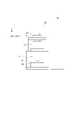
まず、本実施形態に係る露光装置および塗布現像装置の構成について説明する。図1は、露光装置及び塗布現像装置の構成を示した図である。この露光装置および塗布現像装置は、例えば半導体デバイスの製造工程におけるリソグラフィー工程に採用されるものであり、製造工場内のクリーンルームにて、露光装置2と塗布現像装置3とが互いに隣設するように設置されている。露光装置2は、マスク(原版、レチクル)に形成されたパターンを、表面にレジスト(感光剤)膜が形成された基板(ウエハ)に露光処理を行う装置である。また、塗布現像装置3は、露光装置2による露光処理の前処理(前工程)としてレジストを基板の表面上に塗布する塗布処理と、露光処理の後処理(後工程)としてパターンが転写された基板を現像する現像処理とを行う装置である。<First Embodiment>
First, the configurations of the exposure apparatus and the coating and developing apparatus according to the present embodiment will be described. FIG. 1 is a diagram showing the configurations of an exposure apparatus and a coating / developing apparatus. The exposure apparatus and the coating / developing apparatus are adopted, for example, in a lithography process in a semiconductor device manufacturing process, so that the
(露光装置)
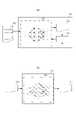
次に、本実施形態に係る露光装置2の構成について説明する。露光装置2は、装置全体を覆うチャンバー4を有し、その内部に、露光処理を実施する本体が収容される露光部5と、塗布現像装置3との基板の受け渡しを実施する基板搬送装置(以下「第1搬送装置」とする)6とを含む。図2は、露光部5の内部に設置される本体20の構成を示す概略図である。この本体20は、ステップ・アンド・リピート方式またはステップ・アンド・スキャン方式を採用し、マスク21に形成されたパターンを基板22に投影露光する投影型露光装置である。なお、図2において、投影光学系の光軸に平行にZ軸を取り、該Z軸に垂直な平面内で、紙面に対して垂直なY軸と該Y軸に対して垂直にX軸とを取って説明する。本体20は、照明装置23と、マスク21を保持するマスクステージ24と、投影光学系25と、基板22を保持する基板ステージ26、マークを撮像する撮像部27とを備える。(Exposure device)
Next, the configuration of the
照明装置23は、不図示の光源と照明光学系とを備え、マスク21を照明する。光源としては、例えばパルス光源(レーザ)を使用する。使用可能なレーザは、波長約193nmのArFエキシマレーザや、波長約153nmのF2エキシマレーザなどである。なお、レーザの種類は、エキシマレーザに限定されず、例えば、YAGレーザを使用しても良いし、レーザの個数も限定されない。また、光源にレーザが使用される場合には、レーザ光源からの平行光束を所望のビーム形状に整形する光束整形光学系や、コヒーレントなレーザをインコヒーレント化するインコヒーレント光学系を使用することが好ましい。更に、使用可能な光源は、パルス光源に限定されるものではなく、一または複数の水銀ランプやキセノンランプなどの連続光源も使用可能である。照明光学系は、レンズ、ミラー、ライトインテグレーターまたは絞りなどを含む。 The
マスク21は、例えば石英ガラス製の原版であり、転写されるべきパターン(例えば回路パターン)が形成されている。マスクステージ24は、マスク21を保持しつつ、XY方向に移動可能とする。投影光学系25は、照明装置23からの露光光で照明されたマスク21上のパターンを所定倍率(例えば1/4または1/5)で基板22上に投影露光する。 The
投影光学系25としては、複数の屈折レンズ要素のみから構成される光学系や、複数の屈折レンズ要素と少なくとも1枚の凹面鏡とから構成される光学系(カタディオプトリック光学系)が採用可能である。または、投影光学系25として、複数の屈折レンズ要素と少なくとも1枚のキノフォームなどの回折光学要素とから構成される光学系や、全ミラー型の光学系なども採用可能である。 As the projection
基板22は、表面上にレジストが塗布された、例えば単結晶シリコンからなる被処理基板である。また、基板ステージ26は、基板22を保持しつつ、XY方向に移動可能とする。例えば、ステップ・アンド・スキャン方式を採用する場合には、マスクステージ24と基板ステージ26とは、それぞれ同期して平行移動することになる。 The
撮像部27は、基板ステージ26に保持された基板22の位置決め(アライメント)を行うために、基板22に形成されたマークを撮像した画像を取得する。撮像部27は、光を照射する光源27a(不図示)と、光源27aから光が照射された撮像対象(基板22)で反射された反射光を受光して、撮像対象を撮像するカメラ27b(不図示)を有する。カメラ27bは、基板22からの反射光の明るさ、即ち濃淡に応じた濃淡画像を出力するイメージセンサ(不図示)と、そのイメージセンサから得られる濃淡画像をデジタル画像信号に変換するA/D変換器(不図示)を備える。後述の第1制御部7は、取得されたデジタル画像信号を用いて基板22に形成されたマークの位置を検出して、検出したマークの位置に基づき基板ステージ26を制御して基板22の位置決めを行う。また、撮像部27は基板ステージ26に形成された基準マーク(不図示)を撮像した画像を取得して、第1制御部7は基板ステージ26に形成された基準マークの位置を検出して、基板ステージ26の位置決めを行うこともできる。 The
第1搬送装置6は、まず、露光処理に先立ち、予め基板の位置決めを実施するプリアライメント部30と、該プリアライメント部30から本体20内の基板ステージ26へ基板を供給する供給ハンド31とを備える。また、第1搬送装置6は、複数の基板を収納可能なオープンカセットを用いて本体20内に直接基板を搬入する場合に、オープンカセットを載置する部位としてのキャリアポート32を備える。なお、このキャリアポート32は、オープンカセットに代えて、密閉型のキャリアであるFOUP(Front Opening Unified Pod)を載置する構造としてもよい。また、第1搬送装置6は、露光装置2と塗布現像装置3との間にて基板の受け渡しを実施する際の第1受け渡し部として第1搬入部33および第1搬出部34と、第1搬送装置6を構成する各部位に基板を適宜搬送する搬送ハンド35とを備える。この搬送ハンド35は、例えば水平多関節型のロボット(スカラーロボット)である。なお、第1搬入部33は、塗布現像装置3から露光装置2へ未露光基板を搬入する際の受け渡し部であるが、プリアライメント部30のようなプリアライメント処理部や温度調節部などのプロセス処理部を兼ね備えていてもよい。一方、第1搬出部34は、露光装置2から塗布現像装置3へ露光済み基板を搬出する際の受け渡し部であるが、周辺露光処理部などのプロセス処理部を兼ね備えていてもよい。 First, the first transfer device 6 includes a
さらに、露光装置2は、例えばコンピュータなどで構成され、露光装置2の各構成要素に回線を介して接続され、プログラムなどにしたがって各構成要素の制御を実行し得る制御部(以下「第1制御部7」とする)を備える。なお、第1制御部7は、露光装置2の内部に一体で構成してもよいし、露光装置2の他の部分とは別の場所に設置してもよい。 Further, the
図3は、情報処理装置の構成を示す図である。第1制御部7は、塗布現像装置3と通信可能に接続された情報処理装置(コンピュータ)300によって実現されうる。図3において、処理部301は、OS(Operating System)及び各種アプリケーションプログラムを実行する中央演算処理装置(CPU)ある。また、処理部301は中央演算処理装置に限られず、マイクロプロセッシングユニット(MPU)、グラフィクスプロセッシングユニット(GPU)、特定用途向け集積回路(ASIC)等のプロセッサ又は回路であってもよい。また、処理部301は、デジタルシグナルプロセッサ(DSP)、データフロープロセッサ(DFP)、またはニューラルプロセッシングユニット(NPU)等のプロセッサ又は回路であってもよい。また、処理部301は、これらのプロセッサ又は回路のいずれかの組合せであってもよい。ROM302は、処理部301が実行するプログラムや演算用のパラメータのうちの固定的なデータを格納するメモリである。RAM303は、処理部301の作業領域やデータの一時記憶領域を提供するメモリである。ROM302及びRAM303は、バス308を介して処理部301に接続される。305はマウス、キーボードなどを含む入力装置(入力部)、306はCRTや液晶ディスプレイなどの表示装置(表示部)である。また、入力装置305及び表示装置306は、タッチパネル等の一体型の装置であってもよい。また、入力装置305及び表示装置306は、情報処理装置300とは別体の装置として構成されてもよい。304は、ハードディスク装置、CD、DVD、メモリカード等の記憶装置であり、各種プログラムや各種データ等を記憶する。入力装置305、表示装置306、及び記憶装置304はそれぞれ、不図示のインタフェースを介してバス308に接続されている。また、ネットワークに接続して通信を行うための通信装置307も、バス308に接続されている。通信装置307は、例えばLANに接続してTCP/IP等の通信プロトコルによるデータ通信を行い、他の通信装置と相互に通信を行う場合に使用される。通信装置307は、データの送信部および受信部として機能し、例えば、塗布現像装置3からデータを受信して、記憶装置304に記憶する。 FIG. 3 is a diagram showing a configuration of an information processing device. The
(塗布現像装置)
次に、本実施形態に係る塗布現像装置3の構成について説明する。塗布現像装置3は、図1に示すように、チャンバー40の内部に設置される塗布現像処理部8と、チャンバー41の内部に設置される、露光装置2との基板の受け渡しを実施する基板搬送装置(以下「第2搬送装置」とする)9とを含む。塗布現像処理部8は、基板に対するプロセス処理部として、塗布部44と、加熱部45と、現像部46と、冷却部47とを備える。塗布部44は、例えばスピンコータを採用し、水平に載置した基板の表面上に、レジストを滴下した状態で基板を回転させることにより、均一なレジスト膜を形成する。加熱部45は、未露光基板に対するプリベーク(PreBake)と、露光済み基板に対する現像前ベーク(Post Exposure Bake)を実施する。プリベークは、基板の表面上にレジストを塗布した後、レジスト膜中の残留溶剤の蒸発と、レジスト膜と基板面との密着性の強化のために実施する熱処理である。このプリベークは、未露光状態(露光前)の基板に対して実施するため、ポリマー処理が重合したり、添加物の熱分解が生じたりしない温度で実施することが望ましい。一方、現像前ベークは、単一波長の光で露光した場合の定在波効果によるレジストパターンの変形を低減するために、露光後かつ現像処理前の基板に対して実施する熱処理である。さらに、現像前ベークは、化学増幅レジストの露光後の触媒反応を促進させる効果もある。なお、加熱部45におけるベーク処理の方式としては、抵抗加熱方式や赤外線加熱方式などが採用可能である。(Coating and developing equipment)
Next, the configuration of the coating and developing apparatus 3 according to the present embodiment will be described. As shown in FIG. 1, the coating and developing apparatus 3 transfers a substrate between the coating and developing processing unit 8 installed inside the
現像部46は、露光済み基板の現像を実施する。現像部46における現像処理の方式としては、スピン式やスプレー式などが採用可能である。冷却部47は、例えば冷却水の循環などにより冷却されるクーリングプレートを採用し、熱を帯びた基板の冷却を実施する。なお、冷却部47における冷却処理の他の方式としては、ペルチェ効果による電子冷却などもある。さらに、塗布現像処理部8は、オープンカセットまたはFOUP等のキャリアを載置する部位としてのキャリアポート48と、キャリアと各プロセス処理部との間で基板を適宜搬送する搬送ハンド49とを備える。この搬送ハンド49は、例えばスカラーロボットである。なお、このようなオープンカセットまたはFOUPは、手動型の搬送台車(PGV:Person Giuded Vehicle)によりクリーンルーム内で搬送され、キャリアポート48に対して自動的に搬入出され得る。これに対して、オープンカセットまたはFOUPをOHT(Over Head Transfer)によりクリーンルーム内の上方からキャリアポート48へ載置する構成もあり得る。 The developing
第2搬送装置9は、露光装置2と塗布現像装置3との間にて基板の受け渡しを実施する際の第2受け渡し部として第2搬入部50および第2搬出部51を備える。また、第2搬送装置9は、第2搬入部50および第2搬出部51と、第1搬送装置6に設置された第1搬入部33および第1搬出部34との間で基板を適宜搬送する搬送ハンド52を備える。この搬送ハンド52は、例えばスカラーロボットである。なお、第2搬入部50は、露光装置2から塗布現像処理部8へ露光済み基板を搬入する際の受け渡し部であり、一方、第2搬出部51は、塗布現像処理部8から露光装置2へ未露光基板を搬出する際の受け渡し部である。 The second transfer device 9 includes a second carry-in
さらに、塗布現像装置3は、例えばコンピュータなどで構成され、塗布現像装置3の各構成要素に回線を介して接続され、プログラムなどにしたがって各構成要素の制御を実行し得る制御部(以下「第2制御部10」とする)を備える。また、第2制御部10は、第1制御部7と同様に、例えば、図3に示される情報処理装置で構成される。なお、第2制御部10は、塗布現像装置3の内部に一体で構成してもよいし、塗布現像装置3の他の部分とは別の場所に設置してもよい。 Further, the coating / developing apparatus 3 is composed of, for example, a computer or the like, is connected to each component of the coating / developing apparatus 3 via a line, and can execute control of each component according to a program or the like (hereinafter, “No. 1”). 2
次に、露光装置および塗布現像装置における処理動作について説明する。以下、被処理基板である基板は、25枚を1ロットとしてオープンカセットに収納され、塗布現像装置3における塗布現像処理部8のキャリアポート48に搬送されてきたと仮定する。まず、塗布現像処理部8において、搬送ハンド49は、キャリアポート48に載置されたオープンカセットから基板を取得して塗布部44に搬送し、塗布部44は、搬入された基板に対してレジストの塗布を実施する。次に、搬送ハンド49は、レジストの塗布が完了した基板を塗布部44から搬出して加熱部45に搬送し、加熱部45は、基板に対してプリベーク処理を実施する。次に、搬送ハンド49は、プリベーク処理が完了した基板を加熱部45より搬出して冷却部47に搬送し、冷却部47は、基板に対して冷却処理を実施する。ここで、後に露光装置2に搬入させる基板の温度は、露光装置2のチャンバー4の内部で影響のない温度、すなわち、本体20内の空調系の温度を目標温度として調節することが望ましい。ただし、本実施形態の露光装置2において、第1搬送装置6内の第1搬入部33にも温度調節部を設置するものとすれば、塗布現像装置3から搬入された基板を最終的かつ精細に温度調節することができる。したがって、冷却部47では、基板の温度が目標温度にある程度近くなっていればよく、最終的な目標温度よりも若干高めの温度であってもよい。次に、搬送ハンド49は、所望の目標温度にまで冷却された基板を冷却部47から搬出して、第2搬出部51に搬送する。搬送ハンド49は、このようにオープンカセットに収納されている基板を順次取得して、各プロセス処理部に搬送する。そして、第2搬送装置9内の搬送ハンド52は、第2搬出部51に保持された基板を、露光装置2における第1搬送装置6内の第1搬入部33へ搬送する。 Next, the processing operation in the exposure apparatus and the coating / developing apparatus will be described. Hereinafter, it is assumed that 25 substrates are stored in an open cassette as one lot and conveyed to the carrier port 48 of the coating development processing unit 8 in the coating development apparatus 3. First, in the coating and developing processing unit 8, the
次に、他方の第1搬送装置6において、第1搬入部33は、その内部の温度調節部にて基板の温度を上記のような所定の温度に調節する。次に、搬送ハンド35は、温度調節が完了した基板を第1搬入部33から搬出し、プリアライメント部30に搬送する。このプリアライメント部30では、基板は、内部のステージ上に載置され、不図示の駆動系により回転される。このとき、CCDセンサなどの検出器により、基板のエッジ部の検出が行われ、制御部7は、この検出器からの出力に基づいて、ノッチ方向、基板中心および偏心量を算出する。そして、プリアライメント部30は、最終的に基板に形成されたノッチ部の方向を所定の方向に合わせる。次に、供給ハンド31は、プリアライメント処理が完了した基板をプリアライメント部30から搬出して本体20内の基板ステージ26へ供給し、本体20は、基板に対して露光処理を実施する。 Next, in the other first transport device 6, the first carry-in
露光処理の完了後、搬送ハンド35は、露光済み基板を基板ステージ26から取得し、第1搬出部34へ搬送する。次に、第2搬送装置9内の搬送ハンド52は、第1搬出部34から第2搬入部50へ基板を搬送し、引き続き、塗布現像処理部8内の搬送ハンド49は、第2搬入部50から加熱部45へ基板を搬送する。次に、加熱部45は、搬入された基板に対して現像前ベークを実施する。次に、搬送ハンド49は、現像前ベーク処理が完了した基板を加熱部45から搬出して現像部46に搬送し、基板に対して現像処理を実施する。そして、搬送ハンド49は、現像処理が完了した基板を現像部46から搬出し、キャリアポート48に載置されているオープンカセットの所定のスロットに搬入する。 After the exposure process is completed, the
本実施形態に係る検査処理では、まず、検査に用いられる基板(以下、検査基板とする)を用意する。検査基板は塗布現像装置3に搬送され、塗布現像装置3によって検査基板に塗布処理が行われ検査基板上にレジスト膜が形成される。次に、レジスト膜が形成された検査基板が露光装置2に搬送され、露光装置2によって検査基板に露光処理が行われレジスト膜が露光される。このとき、パターンが形成されたマスクを用いずに検査基板上の複数の検査領域に対して、露光量を変化させながら順次、露光が行われる。そして、再度、露光された検査基板が塗布現像装置3に搬送され、塗布現像装置3によって検査基板に現像処理が行われ検査基板上のレジスト膜の一部が除去される。 In the inspection process according to the present embodiment, first, a substrate used for the inspection (hereinafter referred to as an inspection substrate) is prepared. The inspection board is conveyed to the coating and developing apparatus 3, and the coating and developing apparatus 3 performs a coating process on the inspection substrate to form a resist film on the inspection substrate. Next, the inspection substrate on which the resist film is formed is conveyed to the
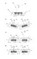
図4は、検査基板上の検査領域を示した図である。図4の例では、検査基板S上には検査領域としてR1~R49が形成されているが、検査領域の大きさ、数、位置などは、この例に限られない。また、検査領域R1~R49には、露光処理において露光量がそれぞれ異なるように、順次露光が行われる。 FIG. 4 is a diagram showing an inspection area on the inspection board. In the example of FIG. 4, R1 to R49 are formed as inspection regions on the inspection substrate S, but the size, number, position, and the like of the inspection regions are not limited to this example. Further, the inspection areas R1 to R49 are sequentially exposed so that the exposure amount is different in the exposure process.
ここで、露光処理における露光量が不足していた場合、検査領域において現像処理が十分に行われず、レジスト膜が残存する部分がある。図5は、複数の検査領域における現像状態を示す図である。図5の例では、検査領域R1~R4の現像状態を表している。また、露光処理において、検査領域R1~R4の順番で露光量が増加した例を示している。ここでは、検査領域R1~R4の露光量をE1~E4とする。露光量E1~E4のうち最も小さい露光量E1で露光された検査領域R1では、領域の全部でレジスト膜が残存している。また、次に小さい露光量E2で露光された検査領域R2では、検査領域R2の四隅の付近で一部のレジスト膜が残存している。また、次に小さい露光量E3で露光された検査領域R3では、検査領域R3の四隅の付近で一部のレジスト膜が残存している。また、検査領域R3におけるレジスト膜が残存している部分は検査領域R2におけるレジスト膜が残存している部分よりも小さい。また、露光量E1~E4のうち最も大きい露光量E4で露光された検査領域R4では、領域の全部でレジスト膜が除去されて残存していない。 Here, if the exposure amount in the exposure process is insufficient, the development process is not sufficiently performed in the inspection region, and there is a portion where the resist film remains. FIG. 5 is a diagram showing a developed state in a plurality of inspection regions. In the example of FIG. 5, the developed state of the inspection areas R1 to R4 is shown. Further, in the exposure process, an example in which the exposure amount is increased in the order of the inspection regions R1 to R4 is shown. Here, the exposure amounts of the inspection areas R1 to R4 are set to E1 to E4. In the inspection region R1 exposed to the smallest exposure amount E1 among the exposure amounts E1 to E4, the resist film remains in the entire region. Further, in the inspection region R2 exposed with the next smallest exposure amount E2, a part of the resist film remains in the vicinity of the four corners of the inspection region R2. Further, in the inspection region R3 exposed with the next smallest exposure amount E3, a part of the resist film remains in the vicinity of the four corners of the inspection region R3. Further, the portion of the inspection region R3 where the resist film remains is smaller than the portion of the inspection region R2 where the resist film remains. Further, in the inspection region R4 exposed to the largest exposure amount E4 among the exposure amounts E1 to E4, the resist film is removed in the entire region and does not remain.
ここで、上記の説明では、露光処理により露光されたレジスト膜の部分が現像処理により除去されることを前提としている。露光処理により露光された部分が現像処理により除去されるレジスト膜はポジレジストによって形成されている。一方、露光処理により露光された部分以外が現像処理により除去されるレジスト膜は、ネガレジストによって形成されている。レジスト膜がネガレジストによって形成されている場合、図5は検査領域R1~R4の順番で露光量が減少した例を示している。 Here, in the above description, it is premised that the portion of the resist film exposed by the exposure process is removed by the development process. The resist film from which the portion exposed by the exposure process is removed by the development process is formed by a positive resist. On the other hand, the resist film in which the portion other than the portion exposed by the exposure treatment is removed by the development treatment is formed by a negative resist. When the resist film is formed of a negative resist, FIG. 5 shows an example in which the exposure amount is reduced in the order of the inspection regions R1 to R4.
このように、検査基板S上の検査領域R1~R4における現像されたレジスト膜の残存状態(以下、現像状態とする)を検査することにより、検査基板S上の検査領域における現像状態と露光量との関係を取得することができる。 In this way, by inspecting the residual state (hereinafter referred to as the developed state) of the developed resist film in the inspection areas R1 to R4 on the inspection board S, the developed state and the exposure amount in the inspection area on the inspection board S. You can get the relationship with.
従来、検査基板S上の検査領域における現像状態を判定するためには、専門的な知識と経験を有する人間がSEM(Scanning Electron Microscope)や光学顕微鏡等を用いて検査基板S上の検査領域を観察する必要があった。また、複数の人間で検査をする場合、検査領域においてレジスト膜が適切なレベルまで除去されているか否かの判定基準が検査を行う人間によって異なり、判定結果にばらつきが生じるという問題もあった。 Conventionally, in order to determine the development state in the inspection area on the inspection board S, a person having specialized knowledge and experience uses an SEM (Scanning Electron Microscope), an optical microscope, or the like to detect the inspection area on the inspection board S. I had to observe. Further, when the inspection is performed by a plurality of humans, the criterion for determining whether or not the resist film is removed to an appropriate level in the inspection region differs depending on the person performing the inspection, and there is a problem that the determination result varies.
そこで、本実施形態に係る検査処理は、機械学習により取得された学習モデルに検査基板S上の検査領域の画像が入力されることで、検査領域の現像状態を示す情報が出力される。また、本実施形態に係る検査処理は、図2に示すような情報処理装置300によって実行される。また、本実施形態に係る検査処理は、第1制御部7、又は第2制御部10によって実行されてもよいし、他の情報処理装置(不図示)によって実行されてもよい。 Therefore, in the inspection process according to the present embodiment, the image of the inspection area on the inspection board S is input to the learning model acquired by machine learning, and the information indicating the development state of the inspection area is output. Further, the inspection process according to the present embodiment is executed by the
図6は、情報処理装置における検査方法を示す図である。本実施形態に係る検査処理は、図3に示される情報処理装置300によって実行される。また、本実施形態に係る検査処理は、露光装置2の第1制御部7、又は塗布現像装置3の第2制御部10によって実行されてもよいし、他の情報処理装置(不図示)によって実行されてもよい。 FIG. 6 is a diagram showing an inspection method in the information processing apparatus. The inspection process according to the present embodiment is executed by the
処理部301は、学習部201、検査部202から構成される。学習部201は、記憶装置304から取得した学習データ211を用いた学習により学習モデル213を取得する。 The
ここで、学習データ211は、入力データ221として現像処理が行われた検査基板(第1基板)上の検査領域が撮像された画像を含む。また、学習データ211は、教師データ222として現像処理が行われた検査基板上の検査領域の現像状態を示す情報を含む。また、検査領域の現像状態を示す情報を、検査領域の現像状態を数値で示す情報とすることができる。例えば、図5における検査領域R1~R4の現像状態について、検査領域R1の現像状態を0%とし、検査領域R2の現像状態を33%とし、検査領域R3の現像状態を66%とし、検査領域R4の現像状態を100%とすることができる。 Here, the learning
また、検査領域の現像状態を示す情報を、検査領域の現像状態の合否を示す情報とすることができる。例えば、図5における検査領域R1~R4の現像状態について、検査領域R1及びR2の現像状態を不合格とし、検査領域R3及びR4の現像状態を合格とすることができる。また、入力データ221と教師データ222との複数の組み合わせを含む情報を学習データ211とする。また、教師データ222に含まれる検査領域の現像状態を示す情報は、例えば、人間が入力データ221に含まれる検査領域の画像を観察して、検査領域の現像状態の検査を行った検査結果に基づいて取得される。 Further, the information indicating the development state of the inspection area can be used as the information indicating the pass / fail of the development state of the inspection area. For example, regarding the developed state of the inspection areas R1 to R4 in FIG. 5, the developed state of the inspection areas R1 and R2 can be rejected, and the developed state of the inspection areas R3 and R4 can be passed. Further, the information including a plurality of combinations of the
ここで、現像処理が行われた検査基板上の検査領域の画像により、図5に示すように現像処理によりレジスト膜が除去された部分とレジスト膜が残存している部分が識別されうる。また、レジスト膜がポジレジストによって形成されている場合、レジスト膜が除去された部分が多いほど現像状態がよいことになる。一方、レジスト膜がネガレジストによって形成されている場合、レジスト膜が除去された部分以外が多いほど現像状態がよいことになる。よって、現像処理が行われた検査基板上の検査領域の画像は、検査領域の現像状態と相関関係を有する。また、前述したように検査領域の現像状態は、露光処理における露光量とも関係があるため、現像処理が行われた検査基板上の検査領域の画像は、露光処理における露光量とも相関関係を有する。 Here, as shown in FIG. 5, a portion from which the resist film has been removed and a portion from which the resist film remains can be identified from the image of the inspection region on the inspection substrate subjected to the development treatment. Further, when the resist film is formed by a positive resist, the more the portion from which the resist film is removed, the better the developed state. On the other hand, when the resist film is formed by a negative resist, the more the portion other than the portion from which the resist film has been removed, the better the developed state. Therefore, the image of the inspection area on the inspection board subjected to the development process has a correlation with the development state of the inspection area. Further, as described above, since the developed state of the inspection area is also related to the exposure amount in the exposure process, the image of the inspection area on the inspection substrate on which the development process is performed has a correlation with the exposure amount in the exposure process. ..
図7は、学習部及び検査部におけるデータの流れを示す図である。学習部201は、入力データ221と教師データ222との関係を示す学習データ211を用いた機械学習を行うことにより、学習モデル213を取得する。そして、検査部202は、取得した学習モデル213に新たな入力データ221を入力することにより、出力として検査データ214が出力される。 FIG. 7 is a diagram showing the flow of data in the learning unit and the inspection unit. The
また、学習モデル213は、例えば、ニューラルネットワークにより構成されることができる。ここで、ニューラルネットワークとは、入力層、中間層、出力層といった多層のネットワーク構造を有するモデルである。ここで、学習モデル213はニューラルネットワークにより構成されるとは限らず、例えば、サポートベクターマシンなど他のモデルにより構成されてもよい。また、学習モデル213は、入力データ221と検査データ214の関係を示すテーブルや多項式等を用いて入力データ221と検査データ214を取得するモデルを含んでもよい。 Further, the
次に、学習部201による学習処理について説明する。図8は、学習部201による学習処理を示すフローチャートである。S801において、学習部201は、記憶装置304から学習データ211を取得する。ここで、学習部201は、RAM303から学習データ211を取得してもよいし、通信装置307を介して外部の記憶装置(不図示)に保存された学習データ211を取得してもよい。 Next, the learning process by the
S802において、学習部201は、機械学習により学習モデル213を取得する。例えば、学習モデル213がニューラルネットワークにより構成される場合、学習部201は、誤差逆伝播法等のアルゴリズムを用いることにより、学習モデル213を取得する。学習部201は、ニューラルネットワーク内部の結合重み付け係数等が最適化されることにより学習モデル213が取得される。誤差逆伝播法は、出力データと教師データとの誤差が小さくなるように、各ニューラルネットワークのノード間の結合重み付け係数等を調整する手法である。 In S802, the
図7(a)は、学習部201が機械学習により学習モデル213を取得する際のデータの流れを示す図である。学習部201は、入力層に入力される入力データ221に応じてニューラルネットワークの出力層から出力される検査データ214と、教師データ222との誤差を得る。学習部201は、損失関数215を用いて、ニューラルネットワークからの検査データ214と教師データとの誤差を計算する。学習部201は、得られた誤差に基づいて、その誤差が所定の許容値よりも小さくなるように、ニューラルネットワークのノード間の結合重み付け係数等を更新して、更新された結合重み付け係数等が適用された学習モデル213を取得する。 FIG. 7A is a diagram showing a flow of data when the
S803において、学習部201は、S802で取得した学習モデル213を検査部202に出力する。ここで、学習部201は、学習モデル213を記憶装置304に保存し、検査部202は保存された学習モデル213を取得してもよい。また、学習モデル213はRAM303に保存されてもよいし、通信装置307を介して外部の記憶装置(不図示)に保存されてもよい。 In S803, the
次に、検査部202による検査処理について説明する。図9は、検査部202による検査処理を示すフローチャートである。S901において、検査部202は、記憶装置304から入力データ212を取得する。ここで、検査部202は、RAM303から学習データ211を取得してもよいし、通信装置307を介して外部の記憶装置(不図示)に保存された学習データ211を取得してもよい。ここで、入力データ212は、検査基板(第2基板)上の検査領域が撮像された画像を含む。詳細については、学習データ211に含まれる入力データ221と同様である。 Next, the inspection process by the
S902において、検査部202は、学習部201から学習モデル213を取得する。ここで、検査部202は、RAM303から学習モデル213を取得してもよいし、通信装置307を介して外部の記憶装置(不図示)に保存された学習モデル213を取得してもよい。 In S902, the
S903において、検査部202は、S901で取得した入力データ212を、S902で取得した学習モデル213に入力して、学習モデル213から出力される検査データ214を取得する。ここで、検査データ214は、現像処理が行われた検査基板上の検査領域の現像状態を示す情報を含む。ここで、検査領域の現像状態を示す情報を、検査領域の現像状態を数値で示す情報とすることができる。また、検査領域の現像状態を示す情報を、検査領域の現像状態の合否を示す情報とすることができる。詳細については、学習データ211に含まれる教師データ222と同様である。また、検査部202は、検査データ214を記憶装置304に保存する。また、検査データ214はRAM303に保存されてもよいし、通信装置307を介して外部の記憶装置(不図示)に保存されてもよい。 In S903, the
図7(b)は、検査部202が検査データ214を取得する際のデータの流れを示す図である。検査部202は、入力される入力データ212に応じて学習モデル213から出力される検査データ214を取得する。例えば、学習モデル213がニューラルネットワークにより構成される場合、入力層に入力された入力データ212、及びノード間の結合重み付け係数等に応じて、出力層から出力される検査データ214が取得される。 FIG. 7B is a diagram showing a data flow when the
S904において、検査部202は、S903で取得した検査データ214を表示装置306に出力する。 In S904, the
表示装置306は、検査部202により出力された検査データ214を画面に表示する。図10は、表示装置により表示された画面を示す図である。画面400には、入力データ212に含まれる、検査基板上の検査領域が撮像された画像を表示する表示領域401、及び検査データ214に含まれる、現像処理が行われた検査基板上の検査領域の現像状態を示す情報を表示する表示領域402が表示される。ここで、現像処理が行われた検査基板上の検査領域の現像状態を示す情報として、検査領域の現像状態を数値で示す情報が表示される例を示したが、これに限られない。例えば、表示領域402において、現像処理が行われた検査基板上の検査領域の現像状態を示す情報として、検査領域の現像状態の合否を示す情報が表示されてもよい。また、表示領域402において、検査領域の現像状態を数値で示す情報が表示され、検査領域の現像状態の合否を示す情報として、検査領域の現像状態を数値で示す情報の背景色、文字の色、及びフォントのうち少なくとも1つが変更されて表示されてもよい。 The
ここで、入力データ221、及び入力データ212に含まれる、現像処理が行われた検査基板上の検査領域が撮像された画像を取得する方法について説明する。図11は、検査領域の撮像処理を示したフローチャートである。ここでは、露光装置2において、検査領域の撮像処理が実行される例を説明するが、基板を検査する検査装置など、撮像部を有する他の装置(不図示)によって実行されてもよい。また、基板に形成されたマークを撮像するための撮像部27を用いる例を説明するが、露光装置2内に配置された他の撮像部(不図示)を用いてもよい。 Here, a method of acquiring an image of the inspection area on the inspection board on which the development processing has been performed, which is included in the
S1101において、露光装置2の第1制御部7は、第1搬送装置6により検査基板Sを基板ステージ26に搬送させる。ここで、検査基板Sは既に現像処理まで行われた基板である。 In S1101, the
S1102において、第1制御部7は、検査基板Sの検査領域が撮像部27の撮像領域に位置するように基板ステージ26を移動させ、撮像部27により検査基板Sの検査領域を撮像させる。また、第1制御部7は、撮像された検査基板Sの検査領域の画像データを、記憶装置304に保存する。また、第1制御部7は、撮像された検査基板Sの検査領域の画像データを、RAM303に保存してもよいし、通信装置307を介して外部の記憶装置(不図示)に保存してもよい。 In S1102, the
ここで、基板Sの検査領域を撮像する際の撮像領域は、任意に設定することができる。例えば、図4に示す検査基板Sの全体を含むように撮像領域を設定することができる。また、図5に示すような、すべての検査領域のうち一部の検査領域を含むように撮像領域を設定することができる。このように、広い撮像領域を設定して複数の検査領域を含む画像を1度に取得することにより、撮像処理の時間を短縮することができる。 Here, the imaging region for imaging the inspection region of the substrate S can be arbitrarily set. For example, the imaging region can be set to include the entire inspection board S shown in FIG. Further, as shown in FIG. 5, the imaging region can be set so as to include a part of the inspection region among all the inspection regions. As described above, by setting a wide imaging region and acquiring an image including a plurality of inspection regions at one time, the time of the imaging process can be shortened.
また、図12に示すように1つの検査領域R1を含むように撮像領域R0を設定することができる。複数の検査領域を含む撮像領域よりも狭い撮像領域を設定して、高精細な画像を取得することにより、検査の精度を向上させることができる。 Further, as shown in FIG. 12, the imaging region R0 can be set so as to include one inspection region R1. The accuracy of inspection can be improved by setting an imaging region narrower than the imaging region including a plurality of inspection regions and acquiring a high-definition image.
また、図13に示すように1つの検査領域に対して複数の撮像領域を設定することができる。さらに狭い撮像領域を設定して高精細な画像を取得することにより、さらに検査の精度を向上させることができる。このとき、矩形の検査領域のそれぞれの四隅を含む領域を撮像領域として設定するとよい。これは、図5における検査領域R2、R3で示すように、検査領域の四隅にレジスト膜が残存するためである。つまり、四隅を含む領域を撮像領域として設定することにより、露光量の違いによりレジスト膜が残存しているかがより正確に判定できるからである。 Further, as shown in FIG. 13, a plurality of imaging regions can be set for one inspection region. By setting a narrower imaging area and acquiring a high-definition image, the accuracy of the inspection can be further improved. At this time, it is advisable to set a region including each of the four corners of the rectangular inspection region as an imaging region. This is because the resist film remains at the four corners of the inspection area as shown by the inspection areas R2 and R3 in FIG. That is, by setting the region including the four corners as the imaging region, it is possible to more accurately determine whether the resist film remains due to the difference in the exposure amount.
また、基板Sの検査領域を撮像する際の撮像条件を変更して複数の画像を取得することができる。図14は、撮像部による基板の撮像を示す図である。図14(a)は、基板ステージ26に保持された検査基板S上の検査領域に、撮像部27の光源27aが光を照射して、カメラ27bが検査領域で反射された反射光を受光して、検査領域を撮像する様子を示している。 Further, it is possible to acquire a plurality of images by changing the imaging conditions when imaging the inspection area of the substrate S. FIG. 14 is a diagram showing an image of a substrate by an image pickup unit. In FIG. 14A, the
また、図14(b)は、撮像条件として、基板ステージ26の角度を変更して、撮像部27が検査領域を撮像する様子を示している。基板ステージ26の角度を複数の角度に設定して、撮像部27により撮像することにより、撮像部27は1つの検査領域に対して複数の画像を取得することができる。 Further, FIG. 14B shows a state in which the
また、図14(c)は、撮像条件として、撮像部27から検査基板S上の検査領域までの距離を変更して、撮像部27が検査領域を撮像する様子を示している。かかる距離を複数の距離に設定して、撮像部27により撮像することにより、撮像部27は1つの検査領域に対して複数の画像を取得することができる。また、撮像部27の光源27a及びカメラ27bのうち少なくとも1つから検査基板S上の検査領域までの距離を変更してもよい。また、カメラ27bが焦点距離を変更する機能を有する場合、撮像部27から検査領域までの距離を変更する代わりに、カメラ27bの焦点距離を変更してもよい。 Further, FIG. 14C shows a state in which the
また、図14(d)は、撮像条件として、光源27aから照射される光の波長、光量などの照明条件を変更して、撮像部27が検査領域を撮像する様子を示している。かかる照明条件を複数の照明条件に設定して、撮像部27により撮像することにより、撮像部27は1つの検査領域に対して複数の画像を取得することができる。 Further, FIG. 14D shows a state in which the
このように、1つの検査領域に対して複数の画像を取得することができるので、学習部201が学習モデル213を取得する際に、学習データ211の数を増やすことができる。これにより、取得される学習モデル213より出力される検査データ214が示す検査結果の精度が向上する。また、検査部202が検査データ214を取得する際に、入力データ212を増やすことができる。これにより、複数の検査データ214を取得することができ、複数の検査データ214を用いて検査することができるので、検査結果の精度が向上する。また、撮像条件として、基板ステージ26の角度、検査領域までの距離、及び照明条件のうち少なくとも2つを組み合わせて、撮像条件を変更して撮像部27が検査領域を撮像してもよい。 In this way, since a plurality of images can be acquired for one inspection area, the number of learning
ここで、図11の説明に戻る。S1103において、第1制御部7は、検査基板Sの検査領域の撮像が完了したかを判定する。つまり、第1制御部7は、複数の検査領域を撮像することが予め定められている場合、複数の撮像条件で撮像をすることが予め定められている場合には、検査領域の撮像を繰り返し行う。また、第1制御部7は、検査基板Sの検査領域の撮像が完了していないと判定した場合、処理をS1102に戻す。また、第1制御部7は、検査基板Sの検査領域の撮像が完了したと判定した場合、処理をS1104に進める。 Here, the explanation returns to FIG. In S1103, the
S1104において、第1制御部7は、第1搬送装置6により検査基板Sを基板ステージ26から搬出させる。 In S1104, the
以上、本実施形態に係る情報処理装置によれば、基板の画像を学習モデルに入力することで基板の現像状態を示す情報を取得することができるので、現像された基板の現像状態を検査することができる。 As described above, according to the information processing apparatus according to the present embodiment, since the information indicating the developed state of the substrate can be acquired by inputting the image of the substrate into the learning model, the developed state of the developed substrate is inspected. be able to.
<第2実施形態>
次に、第2実施形態に係る情報処理装置について説明する。なお、ここで言及しない事項は、第1実施形態に従いうる。本実施形態では、検査部202は、図9のフローチャートのS903において取得された検査データ214に基づき、露光装置2において基板22を露光する時の露光量を決定する。<Second Embodiment>
Next, the information processing apparatus according to the second embodiment will be described. Matters not mentioned here may follow the first embodiment. In the present embodiment, the
図15は、露光量の決定処理を示したフローチャートである。S1501において、検査部202は、記憶装置304から検査データ214を取得する。ここで、検査データ214は、第1実施形態で説明したように、検査領域の現像状態を示す情報を含み、例えば、検査領域の現像状態を数値で示す情報や検査領域の現像状態の合否を示す情報とすることができる。 FIG. 15 is a flowchart showing the process of determining the exposure amount. In S1501, the
S1502において、検査部202は、取得された検査データ214を判定する。例えば、検査データ214が検査領域の現像状態を数値で示す情報を含む場合、検査領域の現像状態を数値が予め定めた許容範囲に収まっているかを判定する。また、検査データ214が検査領域の現像状態の合否を示す情報を含む場合、検査領域の現像状態が合格であるか否かを判定する。 In S1502, the
S1503において、検査部202は、合格と判定された検査データ214に対応する露光量を取得する。例えば、検査部202は、S1501で取得された検査データ214のうち、検査領域の現像状態を数値が予め定めた許容範囲に収まっていると判定された検査データ214を合格と判定された検査データ214として取得する。また、例えば、検査部202は、検査領域の現像状態が合格であると判定された検査データ214を合格と判定された検査データ214として取得する。次に、合格と判定された検査データ214に対応する入力データ221の画像に含まれる検査領域が露光された時の露光量を取得する。ここで、検査領域が露光された時の露光量は、検査領域の画像と共に予め記憶装置304等に記憶されているものとする。 In S1503, the
S1504において、検査部202は、S1503で取得された露光量に基づき、露光装置2において基板22を露光する時の露光量を決定する。ここで、複数の検査データ214が合格と判定された検査データ214として取得された場合、検査部202は、取得された複数の露光量のうち最も小さい露光量を、露光装置2において基板22を露光する時の露光量として決定する。 In S1504, the
以上、本実施形態に係る情報処理装置によれば、基板の画像を学習モデルに入力することで基板の現像状態を示す情報を取得することができるので、現像された基板の現像状態を検査することができる。また、現像された基板の現像状態の検査結果に基づき、露光装置において基板を露光する時の露光量を決定することができる。 As described above, according to the information processing apparatus according to the present embodiment, since the information indicating the developed state of the substrate can be acquired by inputting the image of the substrate into the learning model, the developed state of the developed substrate is inspected. be able to. Further, based on the inspection result of the developed state of the developed substrate, the exposure amount when the substrate is exposed in the exposure apparatus can be determined.
<第3実施形態>
次に、第3実施形態に係る情報処理装置について説明する。なお、ここで言及しない事項は、第1実施形態に従いうる。本実施形態では、検査部202は、S903において取得された検査データ214に基づき、露光装置2においてフレアが発生したか否かを検査するための検査データ214を取得する。<Third Embodiment>
Next, the information processing apparatus according to the third embodiment will be described. Matters not mentioned here may follow the first embodiment. In the present embodiment, the
図16は、フレアが発生した状態で露光された検査領域を撮像した画像を示した図である。例えば、露光装置2においてフレアが発生した状態で検査領域R1が露光された場合に、図16に示すように、現像された検査基板Sの検査領域R1を撮像した画像に特有の模様が発生する。 FIG. 16 is a diagram showing an image of an inspection region exposed in a state where flare is generated. For example, when the inspection region R1 is exposed in a state where flare is generated in the
そこで、検査領域の現像状態を示す情報として検査基板Sが露光された際にフレアが発生した否かを示す情報を、学習データ211の教師データ222に含める。これにより、学習部201により取得される学習モデル213は、検査データ214としてフレアが発生した否かを示す情報を出力することができるようになる。また、検査部202は、検査基板S上の検査領域R1が撮像された画像を含む入力データ212を、かかる学習モデル213に入力することにより、検査基板Sが露光された際にフレアが発生した否かを示す情報を含む検査データ214を取得することができる。 Therefore, as information indicating the development state of the inspection region, information indicating whether flare has occurred when the inspection substrate S is exposed is included in the
以上、本実施形態に係る情報処理装置によれば、基板の画像を学習モデルに入力することで、基板が露光された際にフレアが発生したか否かを検査することができる。 As described above, according to the information processing apparatus according to the present embodiment, by inputting the image of the substrate into the learning model, it is possible to inspect whether or not flare has occurred when the substrate is exposed.
<第4実施形態>
次に、第4実施形態に係る情報処理装置について説明する。なお、ここで言及しない事項は、第1実施形態に従いうる。本実施形態では、検査部202は、S903において取得された検査データ214に基づき、露光装置2に含まれる光学素子に異常が発生したか否かの検査するための検査データ214を取得する。<Fourth Embodiment>
Next, the information processing apparatus according to the fourth embodiment will be described. Matters not mentioned here may follow the first embodiment. In the present embodiment, the
図17は、光学素子に異常が発生した状態で露光された検査領域を撮像した画像を示した図である。例えば、露光装置2に含まれる光学素子に傷がある状態やかかる光学素子に異物が付着した状態で検査領域R1が露光された場合に、図17に示すように、現像された検査基板Sの検査領域R1を撮像した画像に特有の形状を有する領域が発生する。ここで、露光装置2に含まれる光学素子には、露光装置2の照明装置23、及び投影光学系25に含まれる光学素子が含まれうる。 FIG. 17 is a diagram showing an image of an inspection region exposed in a state where an abnormality has occurred in an optical element. For example, when the inspection region R1 is exposed in a state where the optical element included in the
そこで、検査領域の現像状態を示す情報として光学素子に異常が発生した否かを示す情報を、学習データ211の教師データ222に含める。これにより、学習部201により取得される学習モデル213は、検査データ214として光学素子に異常が発生した否かを示す情報を出力することができるようになる。また、検査部202は、検査基板S上の検査領域R1が撮像された画像を含む入力データ212を、かかる学習モデル213に入力することにより、光学素子に異常が発生した否かを示す情報を含む検査データ214を取得することができる。 Therefore, as information indicating the development state of the inspection region, information indicating whether or not an abnormality has occurred in the optical element is included in the
以上、本実施形態に係る情報処理装置によれば、基板の画像を学習モデルに入力することで、基板を露光した露光装置に含まれる光学素子に異常が発生したか否かを検査することができる。 As described above, according to the information processing apparatus according to the present embodiment, by inputting the image of the substrate into the learning model, it is possible to inspect whether or not an abnormality has occurred in the optical element included in the exposure apparatus exposed to the substrate. can.
<物品の製造方法の実施形態>
物品として、例えば、デバイス(半導体デバイス、磁気記憶媒体、液晶表示素子等)、カラーフィルター、又はハードディスク等の製造方法について説明する。かかる製造方法は、露光装置を用いてパターンを基板(ウエハ、ガラスプレート、フィルム状基板等)に形成する工程を含む。かかる製造方法は、パターンを形成された基板を処理する工程を更に含む。該処理ステップは、該パターンの残膜を除去するステップを含みうる。また、該パターンをマスクとして基板をエッチングするステップなどの周知の他のステップを含みうる。本実施形態における物品の製造方法は、従来に比べて、物品の性能、品質、生産性及び生産コストの少なくとも1つにおいて有利である。<Embodiment of manufacturing method of article>
As articles, for example, a method for manufacturing a device (semiconductor device, magnetic storage medium, liquid crystal display element, etc.), a color filter, a hard disk, or the like will be described. Such a manufacturing method includes a step of forming a pattern on a substrate (wafer, glass plate, film-like substrate, etc.) using an exposure apparatus. Such a manufacturing method further includes a step of processing a patterned substrate. The treatment step may include removing the residual film of the pattern. Further, it may include other well-known steps such as a step of etching a substrate using the pattern as a mask. The method for producing an article in the present embodiment is advantageous in at least one of the performance, quality, productivity and production cost of the article as compared with the conventional method.
<他の実施形態>
本発明は、上述の実施形態の1以上の機能を実現するプログラムを、ネットワーク又は記憶媒体を介してシステム又は装置に供給し、そのシステム又は装置のコンピュータにおける1つ以上のプロセッサがプログラムを読み出し実行する処理でも実現可能である。また、1以上の機能を実現する回路(例えば、ASIC)によっても実現可能である。<Other embodiments>
The present invention supplies a program that realizes one or more functions of the above-described embodiment to a system or device via a network or storage medium, and one or more processors in the computer of the system or device reads and executes the program. It can also be realized by the processing to be performed. It can also be realized by a circuit (for example, ASIC) that realizes one or more functions.
以上、本発明の好ましい実施形態について説明したが、本発明はこれらの実施形態に限定されないことはいうまでもなく、その要旨の範囲内で種々の変形及び変更が可能である。 Although the preferred embodiments of the present invention have been described above, it goes without saying that the present invention is not limited to these embodiments, and various modifications and changes can be made within the scope of the gist thereof.
また、第1実施形態乃至第4実施形態は、単独で実施するだけでなく、第1実施形態乃至第4実施形態のうちのいずれの組合せで実施することができる。 Further, the first embodiment to the fourth embodiment can be implemented not only alone but also in any combination of the first embodiment to the fourth embodiment.
Claims (15)
Translated fromJapanese現像された第1基板が撮像された画像と前記第1基板の現像状態を示す情報とを含む学習データを用いた学習により取得された学習モデルに、現像された第2基板が撮像された画像を入力することにより、前記第2基板の現像状態を示す情報を含む検査データを取得する検査部を有する
ことを特徴とする情報処理装置。An information processing device that inspects the development status of a substrate.
An image in which the developed second substrate is imaged on a learning model acquired by training using training data including an image captured by the developed first substrate and information indicating the developed state of the first substrate. An information processing apparatus comprising an inspection unit for acquiring inspection data including information indicating the development state of the second substrate by inputting.
前記検査部は、前記学習部により取得された前記学習モデルを用いて前記検査データを取得することを特徴とする、請求項1に記載の情報処理装置。It has a learning unit that acquires the learning model by learning using the learning data.
The information processing apparatus according to claim 1, wherein the inspection unit acquires the inspection data by using the learning model acquired by the learning unit.
現像された第1基板が撮像された画像と前記第1基板の現像状態を示す情報とを含む学習データを用いた学習により取得された学習モデルに、現像された第2基板が撮像された画像を入力することにより、前記第2基板の現像状態を示す情報を含む検査データを取得する検査工程を有する
ことを特徴とする検査方法。This is an inspection method for inspecting the developed state of the substrate.
An image in which the developed second substrate is imaged on a learning model acquired by training using training data including an image captured by the developed first substrate and information indicating the developed state of the first substrate. An inspection method comprising an inspection step of acquiring inspection data including information indicating the development state of the second substrate by inputting.
前記検査工程において、前記学習工程において取得された前記学習モデルを用いて前記検査データを取得することを特徴とする、請求項9に記載の検査方法。It has a learning process of acquiring the learning model by learning using the learning data.
The inspection method according to claim 9, wherein in the inspection step, the inspection data is acquired by using the learning model acquired in the learning step.
現像された第1基板が撮像された画像と前記第1基板の現像状態を示す情報とを含む学習データを用いた学習により取得された学習モデルに、現像された第2基板が撮像された画像を入力することにより、前記第2基板の現像状態を示す情報を含む検査データを取得する検査工程を有する
ことを特徴とする検査方法をコンピュータに実行させるプログラム。A program that causes a computer to execute an inspection method for inspecting the developed state of a substrate.
An image in which the developed second substrate is imaged on a learning model acquired by learning using training data including an image captured by the developed first substrate and information indicating the developed state of the first substrate. A program for causing a computer to execute an inspection method characterized by having an inspection step of acquiring inspection data including information indicating the development state of the second substrate by inputting.
請求項1乃至8のいずれか1項に記載の情報処理装置と、
基板を撮像する撮像部と、を有し、
前記情報処理装置は、前記撮像部により撮像された画像であって現像された基板を撮像した画像に基づき、前記基板の現像状態を示す情報を含む検査データを取得することを特徴とする露光装置。An exposure device that exposes a substrate
The information processing apparatus according to any one of claims 1 to 8.
It has an image pickup unit that captures an image of a substrate, and has an image pickup unit.
The information processing apparatus is an exposure apparatus characterized in that it acquires inspection data including information indicating a developed state of the substrate based on an image captured by the image pickup unit and an image of the developed substrate. ..
前記露光工程で露光された前記基板を処理する処理工程と、を有し、
前記処理工程で処理された前記基板から物品を製造することを特徴とする物品の製造方法。An exposure step of exposing a substrate using the exposure apparatus according to claim 12.
It has a processing step of processing the substrate exposed in the exposure step.
A method for manufacturing an article, which comprises manufacturing an article from the substrate treated in the processing step.
現像された第1基板が撮像された画像と前記第1基板の現像状態を示す情報とを含む学習データを用いた学習により取得された学習モデルに、現像された第2基板が撮像された画像を入力することにより、前記第2基板の現像状態を示す情報を含む検査データを取得する検査工程と、
前記検査工程で取得された検査データに基づき基板を露光する時の露光量を決定する決定工程と、を有する
ことを特徴とする決定方法。It is a determination method for determining the amount of exposure when exposing a substrate.
An image in which the developed second substrate is imaged on a learning model acquired by training using training data including an image captured by the developed first substrate and information indicating the developed state of the first substrate. By inputting, an inspection step of acquiring inspection data including information indicating the development state of the second substrate, and an inspection step.
A determination method comprising: a determination step of determining an exposure amount when exposing a substrate based on the inspection data acquired in the inspection step.
前記検査工程で取得された検査データに基づき基板を露光する時の露光量を決定する決定工程と、
前記決定工程で決定された露光量で基板を露光する露光工程と、
前記露光工程で露光された前記基板を処理する処理工程と、を有し、
前記処理工程で処理された前記基板から物品を製造することを特徴とする物品の製造方法。An image in which the developed second substrate is imaged on a learning model acquired by training using training data including an image captured by the developed first substrate and information indicating the developed state of the first substrate. By inputting, an inspection step of acquiring inspection data including information indicating the development state of the second substrate, and an inspection step.
A determination step of determining the exposure amount when the substrate is exposed based on the inspection data acquired in the inspection step, and a determination step.
An exposure step of exposing the substrate with the exposure amount determined in the determination step, and an exposure step of exposing the substrate.
It has a processing step of processing the substrate exposed in the exposure step.
A method for manufacturing an article, which comprises manufacturing an article from the substrate treated in the processing step.
Priority Applications (3)
| Application Number | Priority Date | Filing Date | Title |
|---|---|---|---|
| JP2020162585AJP7596106B2 (en) | 2020-09-28 | 2020-09-28 | Information processing apparatus, inspection method, program, exposure apparatus, determination method, and article manufacturing method |
| US17/478,329US20220100081A1 (en) | 2020-09-28 | 2021-09-17 | Information processing apparatus, inspection method, storage medium, exposure apparatus, determination method, and article manufacturing method |
| CN202111118738.4ACN114326318A (en) | 2020-09-28 | 2021-09-24 | Information processing apparatus, inspection method, storage medium, exposure apparatus, determination method, and article manufacturing method |
Applications Claiming Priority (1)
| Application Number | Priority Date | Filing Date | Title |
|---|---|---|---|
| JP2020162585AJP7596106B2 (en) | 2020-09-28 | 2020-09-28 | Information processing apparatus, inspection method, program, exposure apparatus, determination method, and article manufacturing method |
Publications (2)
| Publication Number | Publication Date |
|---|---|
| JP2022055149Atrue JP2022055149A (en) | 2022-04-07 |
| JP7596106B2 JP7596106B2 (en) | 2024-12-09 |
Family
ID=80821117
Family Applications (1)
| Application Number | Title | Priority Date | Filing Date |
|---|---|---|---|
| JP2020162585AActiveJP7596106B2 (en) | 2020-09-28 | 2020-09-28 | Information processing apparatus, inspection method, program, exposure apparatus, determination method, and article manufacturing method |
Country Status (3)
| Country | Link |
|---|---|
| US (1) | US20220100081A1 (en) |
| JP (1) | JP7596106B2 (en) |
| CN (1) | CN114326318A (en) |
Families Citing this family (1)
| Publication number | Priority date | Publication date | Assignee | Title |
|---|---|---|---|---|
| CN114706281B (en)* | 2022-05-18 | 2023-09-19 | 圆周率半导体(南通)有限公司 | Method for improving exposure uniformity of PCB |
Citations (2)
| Publication number | Priority date | Publication date | Assignee | Title |
|---|---|---|---|---|
| JP2019502950A (en)* | 2015-12-17 | 2019-01-31 | エーエスエムエル ネザーランズ ビー.ブイ. | Optical metrology of lithographic processes using asymmetric sub-resolution features to improve measurement |
| JP2019165123A (en)* | 2018-03-20 | 2019-09-26 | 株式会社日立ハイテクノロジーズ | Search device, search method, and plasma processing device |
Family Cites Families (3)
| Publication number | Priority date | Publication date | Assignee | Title |
|---|---|---|---|---|
| JP4005881B2 (en)* | 2002-08-30 | 2007-11-14 | 株式会社東芝 | Inspection method for exposure apparatus |
| CN104884945A (en)* | 2012-12-27 | 2015-09-02 | 株式会社尼康 | Inspection apparatus, inspection method, exposure system, exposure method, and device manufacturing method |
| KR102711835B1 (en)* | 2019-04-04 | 2024-10-02 | 에이에스엠엘 네델란즈 비.브이. | Device and method for predicting substrate image |
- 2020
- 2020-09-28JPJP2020162585Apatent/JP7596106B2/enactiveActive
- 2021
- 2021-09-17USUS17/478,329patent/US20220100081A1/enactivePending
- 2021-09-24CNCN202111118738.4Apatent/CN114326318A/enactivePending
Patent Citations (2)
| Publication number | Priority date | Publication date | Assignee | Title |
|---|---|---|---|---|
| JP2019502950A (en)* | 2015-12-17 | 2019-01-31 | エーエスエムエル ネザーランズ ビー.ブイ. | Optical metrology of lithographic processes using asymmetric sub-resolution features to improve measurement |
| JP2019165123A (en)* | 2018-03-20 | 2019-09-26 | 株式会社日立ハイテクノロジーズ | Search device, search method, and plasma processing device |
Also Published As
| Publication number | Publication date |
|---|---|
| US20220100081A1 (en) | 2022-03-31 |
| JP7596106B2 (en) | 2024-12-09 |
| CN114326318A (en) | 2022-04-12 |
Similar Documents
| Publication | Publication Date | Title |
|---|---|---|
| TWI670563B (en) | Pattern inspection apparatus, pattern position measurement apparatus, aerial image measurement system, method for measuring aerial image, pattern position repairing apparatus, method for repairing pattern position, aerial image data processing apparatus, | |
| TWI448824B (en) | A method, program product and apparatus for performing decomposition of a pattern for use in a dpt process | |
| TWI660235B (en) | Method and non-transitory computer program product for determining a parameter of a patterned substrate | |
| TWI734973B (en) | Lithography device, pattern forming method, and article manufacturing method | |
| TWI471900B (en) | Exposure method, exposure apparatus, exposure system, and device manufacturing method | |
| US11567400B2 (en) | Method of fabricating a photomask and method of inspecting a photomask | |
| US11314172B2 (en) | Instant tuning method for accelerating resist and etch model calibration | |
| US6876439B2 (en) | Method to increase throughput in a dual substrate stage double exposure lithography system | |
| US7400390B2 (en) | Inspection system and a method for aerial reticle inspection | |
| JP7596106B2 (en) | Information processing apparatus, inspection method, program, exposure apparatus, determination method, and article manufacturing method | |
| CN111090216A (en) | Method and apparatus for determining the position of a plurality of pixels introduced into a photolithographic mask substrate | |
| JP6763966B2 (en) | Image processing convolution algorithm for defect detection | |
| JP2005340828A (en) | Lithographic device and device manufacturing method | |
| JP6903133B2 (en) | Multiple image particle detection system and method | |
| US6781674B1 (en) | System and method to increase throughput in a dual substrate stage double exposure lithography system | |
| JP7105582B2 (en) | Determination method, exposure method, exposure apparatus, article manufacturing method and program | |
| TWI792538B (en) | Lithography method, lithography process and lithography system | |
| JP6837159B2 (en) | Anti-reflective coating | |
| JP2019200444A (en) | Lithography deice, pattern formation method, and manufacturing method of article | |
| JP7071483B2 (en) | Lithography equipment, pattern forming method and article manufacturing method | |
| JPH088161A (en) | Transfer simulator device | |
| TW202534442A (en) | Information processing apparatus, pattern forming apparatus, information processing method, and article manufacturing method | |
| JP2025125291A (en) | Information processing apparatus, exposure apparatus, article manufacturing method, substrate processing system, and information processing method | |
| JP2024175984A (en) | Information processing apparatus, exposure apparatus, and acquisition method | |
| NL2025112A (en) | Method for inferring a local uniformity metric and associated appratuses |
Legal Events
| Date | Code | Title | Description |
|---|---|---|---|
| A621 | Written request for application examination | Free format text:JAPANESE INTERMEDIATE CODE: A621 Effective date:20230912 | |
| RD01 | Notification of change of attorney | Free format text:JAPANESE INTERMEDIATE CODE: A7421 Effective date:20231213 | |
| A131 | Notification of reasons for refusal | Free format text:JAPANESE INTERMEDIATE CODE: A131 Effective date:20240820 | |
| A521 | Request for written amendment filed | Free format text:JAPANESE INTERMEDIATE CODE: A523 Effective date:20241011 | |
| TRDD | Decision of grant or rejection written | ||
| A01 | Written decision to grant a patent or to grant a registration (utility model) | Free format text:JAPANESE INTERMEDIATE CODE: A01 Effective date:20241029 | |
| A61 | First payment of annual fees (during grant procedure) | Free format text:JAPANESE INTERMEDIATE CODE: A61 Effective date:20241127 | |
| R150 | Certificate of patent or registration of utility model | Ref document number:7596106 Country of ref document:JP Free format text:JAPANESE INTERMEDIATE CODE: R150 |