JP2022038209A - Semiconductor device - Google Patents
Semiconductor deviceDownload PDFInfo
- Publication number
- JP2022038209A JP2022038209AJP2020142583AJP2020142583AJP2022038209AJP 2022038209 AJP2022038209 AJP 2022038209AJP 2020142583 AJP2020142583 AJP 2020142583AJP 2020142583 AJP2020142583 AJP 2020142583AJP 2022038209 AJP2022038209 AJP 2022038209A
- Authority
- JP
- Japan
- Prior art keywords
- oxide semiconductor
- semiconductor layer
- electrode
- oxide
- region
- Prior art date
- Legal status (The legal status is an assumption and is not a legal conclusion. Google has not performed a legal analysis and makes no representation as to the accuracy of the status listed.)
- Pending
Links
Images


Classifications
- H—ELECTRICITY
- H01—ELECTRIC ELEMENTS
- H01L—SEMICONDUCTOR DEVICES NOT COVERED BY CLASS H10
- H01L21/00—Processes or apparatus adapted for the manufacture or treatment of semiconductor or solid state devices or of parts thereof
- H01L21/02—Manufacture or treatment of semiconductor devices or of parts thereof
- H01L21/02104—Forming layers
- H01L21/02365—Forming inorganic semiconducting materials on a substrate
- H01L21/02518—Deposited layers
- H01L21/02521—Materials
- H01L21/02565—Oxide semiconducting materials not being Group 12/16 materials, e.g. ternary compounds
- H—ELECTRICITY
- H10—SEMICONDUCTOR DEVICES; ELECTRIC SOLID-STATE DEVICES NOT OTHERWISE PROVIDED FOR
- H10B—ELECTRONIC MEMORY DEVICES
- H10B12/00—Dynamic random access memory [DRAM] devices
- H10B12/30—DRAM devices comprising one-transistor - one-capacitor [1T-1C] memory cells
- H10B12/33—DRAM devices comprising one-transistor - one-capacitor [1T-1C] memory cells the capacitor extending under the transistor
- H—ELECTRICITY
- H01—ELECTRIC ELEMENTS
- H01L—SEMICONDUCTOR DEVICES NOT COVERED BY CLASS H10
- H01L21/00—Processes or apparatus adapted for the manufacture or treatment of semiconductor or solid state devices or of parts thereof
- H01L21/02—Manufacture or treatment of semiconductor devices or of parts thereof
- H01L21/02104—Forming layers
- H01L21/02365—Forming inorganic semiconducting materials on a substrate
- H01L21/02436—Intermediate layers between substrates and deposited layers
- H01L21/02439—Materials
- H01L21/02483—Oxide semiconducting materials not being Group 12/16 materials, e.g. ternary compounds
- H—ELECTRICITY
- H01—ELECTRIC ELEMENTS
- H01L—SEMICONDUCTOR DEVICES NOT COVERED BY CLASS H10
- H01L21/00—Processes or apparatus adapted for the manufacture or treatment of semiconductor or solid state devices or of parts thereof
- H01L21/02—Manufacture or treatment of semiconductor devices or of parts thereof
- H01L21/02104—Forming layers
- H01L21/02365—Forming inorganic semiconducting materials on a substrate
- H01L21/02518—Deposited layers
- H01L21/02587—Structure
- H01L21/0259—Microstructure
- H01L21/02592—Microstructure amorphous
- H—ELECTRICITY
- H10—SEMICONDUCTOR DEVICES; ELECTRIC SOLID-STATE DEVICES NOT OTHERWISE PROVIDED FOR
- H10B—ELECTRONIC MEMORY DEVICES
- H10B12/00—Dynamic random access memory [DRAM] devices
- H10B12/01—Manufacture or treatment
- H10B12/02—Manufacture or treatment for one transistor one-capacitor [1T-1C] memory cells
- H10B12/03—Making the capacitor or connections thereto
- H10B12/036—Making the capacitor or connections thereto the capacitor extending under the transistor
- H—ELECTRICITY
- H10—SEMICONDUCTOR DEVICES; ELECTRIC SOLID-STATE DEVICES NOT OTHERWISE PROVIDED FOR
- H10B—ELECTRONIC MEMORY DEVICES
- H10B12/00—Dynamic random access memory [DRAM] devices
- H10B12/01—Manufacture or treatment
- H10B12/02—Manufacture or treatment for one transistor one-capacitor [1T-1C] memory cells
- H10B12/05—Making the transistor
- H—ELECTRICITY
- H10—SEMICONDUCTOR DEVICES; ELECTRIC SOLID-STATE DEVICES NOT OTHERWISE PROVIDED FOR
- H10D—INORGANIC ELECTRIC SEMICONDUCTOR DEVICES
- H10D30/00—Field-effect transistors [FET]
- H10D30/60—Insulated-gate field-effect transistors [IGFET]
- H10D30/67—Thin-film transistors [TFT]
- H10D30/6728—Vertical TFTs
- H—ELECTRICITY
- H10—SEMICONDUCTOR DEVICES; ELECTRIC SOLID-STATE DEVICES NOT OTHERWISE PROVIDED FOR
- H10D—INORGANIC ELECTRIC SEMICONDUCTOR DEVICES
- H10D30/00—Field-effect transistors [FET]
- H10D30/60—Insulated-gate field-effect transistors [IGFET]
- H10D30/67—Thin-film transistors [TFT]
- H10D30/6729—Thin-film transistors [TFT] characterised by the electrodes
- H—ELECTRICITY
- H10—SEMICONDUCTOR DEVICES; ELECTRIC SOLID-STATE DEVICES NOT OTHERWISE PROVIDED FOR
- H10D—INORGANIC ELECTRIC SEMICONDUCTOR DEVICES
- H10D30/00—Field-effect transistors [FET]
- H10D30/60—Insulated-gate field-effect transistors [IGFET]
- H10D30/67—Thin-film transistors [TFT]
- H10D30/674—Thin-film transistors [TFT] characterised by the active materials
- H10D30/6755—Oxide semiconductors, e.g. zinc oxide, copper aluminium oxide or cadmium stannate
- H10D30/6756—Amorphous oxide semiconductors
- H—ELECTRICITY
- H10—SEMICONDUCTOR DEVICES; ELECTRIC SOLID-STATE DEVICES NOT OTHERWISE PROVIDED FOR
- H10D—INORGANIC ELECTRIC SEMICONDUCTOR DEVICES
- H10D62/00—Semiconductor bodies, or regions thereof, of devices having potential barriers
- H10D62/40—Crystalline structures
- H10D62/402—Amorphous materials
- H—ELECTRICITY
- H10—SEMICONDUCTOR DEVICES; ELECTRIC SOLID-STATE DEVICES NOT OTHERWISE PROVIDED FOR
- H10D—INORGANIC ELECTRIC SEMICONDUCTOR DEVICES
- H10D62/00—Semiconductor bodies, or regions thereof, of devices having potential barriers
- H10D62/80—Semiconductor bodies, or regions thereof, of devices having potential barriers characterised by the materials
- H—ELECTRICITY
- H10—SEMICONDUCTOR DEVICES; ELECTRIC SOLID-STATE DEVICES NOT OTHERWISE PROVIDED FOR
- H10D—INORGANIC ELECTRIC SEMICONDUCTOR DEVICES
- H10D64/00—Electrodes of devices having potential barriers
- H10D64/60—Electrodes characterised by their materials
- H10D64/62—Electrodes ohmically coupled to a semiconductor
- H—ELECTRICITY
- H10—SEMICONDUCTOR DEVICES; ELECTRIC SOLID-STATE DEVICES NOT OTHERWISE PROVIDED FOR
- H10D—INORGANIC ELECTRIC SEMICONDUCTOR DEVICES
- H10D99/00—Subject matter not provided for in other groups of this subclass
Landscapes
- Engineering & Computer Science (AREA)
- Manufacturing & Machinery (AREA)
- Physics & Mathematics (AREA)
- Condensed Matter Physics & Semiconductors (AREA)
- General Physics & Mathematics (AREA)
- Computer Hardware Design (AREA)
- Microelectronics & Electronic Packaging (AREA)
- Power Engineering (AREA)
- Chemical & Material Sciences (AREA)
- Crystallography & Structural Chemistry (AREA)
- Thin Film Transistor (AREA)
- Semiconductor Memories (AREA)
Abstract
Translated fromJapaneseDescription
Translated fromJapanese本発明の実施形態は、半導体装置に関する。 Embodiments of the present invention relate to semiconductor devices.
チャネル領域に酸化物半導体を用いた酸化物半導体トランジスタは、チャネルリーク電流が小さいという特性を有する。このような酸化物半導体トランジスタには、例えばインジウム(In)、錫(Sn)、亜鉛(Zn)、ガリウム(Ga)等の金属元素の1種又は2種以上を含む金属酸化物が用いられている。このような例えばアモルファス構造を有する金属酸化物は、バンドギャップが大きく、移動度が高いといった特徴を有する反面、半導体としての特性が損なわれる場合がある。 An oxide semiconductor transistor using an oxide semiconductor in the channel region has a characteristic that the channel leakage current is small. For such an oxide semiconductor transistor, a metal oxide containing one or more of metal elements such as indium (In), tin (Sn), zinc (Zn), and gallium (Ga) is used. There is. For example, a metal oxide having an amorphous structure has a large bandgap and high mobility, but on the other hand, its characteristics as a semiconductor may be impaired.
本発明が解決しようとする課題は、酸化物半導体の特性を高めることを可能にした半導体装置を提供することにある。 An object to be solved by the present invention is to provide a semiconductor device capable of enhancing the characteristics of an oxide semiconductor.
実施形態の半導体装置は、酸化物半導体層を具備する半導体装置であって、前記酸化物半導体層は、インジウム及び錫からなる群より選ばれる少なくとも1つの第1の金属元素と、亜鉛、ガリウム、アルミニウム、タングステン、及びケイ素からなる群より選ばれる少なくとも1つの第2の金属元素とを含む金属酸化物を備え、前記酸化物半導体層は、前記金属酸化物に対して、フッ素及び塩素からなる群より選ばれる少なくとも1つのアニオン元素が1原子%以上8原子%未満の範囲で含有された第1領域を備える。 The semiconductor device of the embodiment is a semiconductor device including an oxide semiconductor layer, wherein the oxide semiconductor layer contains at least one first metal element selected from the group consisting of indium and tin, and zinc, gallium, and the like. The oxide semiconductor layer comprises a metal oxide containing at least one second metal element selected from the group consisting of aluminum, tungsten, and silicon, and the oxide semiconductor layer is a group consisting of fluorine and chlorine with respect to the metal oxide. It comprises a first region containing at least one anion element selected from the above in the range of 1 atomic% or more and less than 8 atomic%.
以下、実施形態の半導体装置について、図面を参照して説明する。各実施形態において、実質的に同一の構成部位には同一の符号を付し、その説明を一部省略する場合がある。図面は模式的なものであり、厚さと平面寸法との関係、各部の厚さの比率等は現実のものとは異なる場合がある。 Hereinafter, the semiconductor device of the embodiment will be described with reference to the drawings. In each embodiment, substantially the same constituent parts may be designated by the same reference numerals, and the description thereof may be partially omitted. The drawings are schematic, and the relationship between the thickness and the plane dimensions, the ratio of the thickness of each part, etc. may differ from the actual ones.
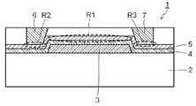
(第1の実施形態)
図1は第1の実施形態の半導体装置としての薄膜トランジスタ(Thin Film Transistor:TFT)1を示している。薄膜トランジスタ1は、チャネルの形成領域となるチャネル層として酸化物半導体層を有するボトムゲート型の酸化物半導体トランジスタである。図1に示すトランジスタ1は、基板2、第1電極としてのゲート電極3、ゲート絶縁膜4、チャネル層としての酸化物半導体層5、第2電極としてのソース電極6、及び第3電極としてのドレイン電極7を備えている。なお、実施形態の半導体装置は、チャネル層として酸化物半導体層を有するトランジスタに限られるものではなく、各種機能を有する酸化物半導体層を備える半導体装置に適用することができる。(First Embodiment)
FIG. 1 shows a thin film transistor (TFT) 1 as a semiconductor device of the first embodiment. The
図1に示す半導体装置1において、ゲート電極3は半導体基板等の基板2上に基板2の面方向である第1方向に延伸して設けられている。ゲート絶縁膜4は、ゲート電極3を覆うように基板2上に設けられている。ゲート電極3上には、ゲート絶縁膜4を介してチャネル層としての酸化物半導体層5が第1方向に延伸して設けられている。酸化物半導体層5の一部は、ゲート絶縁膜4を介してゲート電極3と対向する(例えば積層される)ように配置されている。酸化物半導体層5の第1方向の一端(第1端部)側には、ソース電極6が電気的に接続されるように設けられており、第1方向の他端(第2端部)側にはドレイン電極7が電気的に接続されるように設けられている。 In the
ゲート電極3は、金属、金属化合物、導電性酸化物、半導体等を含む。ゲート電極3は、例えばタングステン(W)、モリブデン(Mo)、銅(Cu)、タンタル(Ta)、アルミニウム(Al)等から選ばれる少なくとも1つの元素を含むことができる。ゲート電極3は、アルミニウムを主成分とするアルミニウム合金を含んでいてもよい。ゲート電極3は、窒化チタン(TiN)や窒化タンタル(TaN)等を含んでいてもよい。ゲート絶縁膜4は、シリコン酸化物(SiO)やシリコン窒化物(SiN)等を含んでいる。ソース電極6及びドレイン電極7には、ゲート電極3と同様な材料が用いられる。 The
酸化物半導体層5は、インジウム(In)及び錫(Sn)からなる群より選ばれる少なくとも1つの第1の金属元素(以下、M1元素と呼ぶこともある。)と、亜鉛(Zn)、ガリウム(Ga)、アルミニウム(Al)、タングステン(W)、及びケイ素(Si)からなる群より選ばれる少なくとも1つの第2の金属元素(以下、M2元素と呼ぶこともある。)とを含む金属酸化物を備える。酸化物半導体層5を構成する金属酸化物としては、In酸化物、Sn酸化物、及びInSn酸化物からなる群より選ばれる1つの酸化物に、Zn、Ga、Al、W、及びSiからなる群より選ばれる少なくとも1つの第2の金属元素(M2元素)を含有させた金属酸化物(M1-M2-O)が挙げられる。 The
M2元素を含むIn酸化物の具体例としては、InZnGaAlWSiO、InZnGaAlWSiO、InGaAlWSiO、InZnAlWSiO、InZnGaWSiO、InZnGaAlWO、InZnGaAlSiO、InAlWSiO、InGaWSiO、InGaAlWO、InGaAlSiO、InZnWSiO、InZnAlWO、InZnAlSiO、InZnGaWO、InZnGaSiO、InZnGaAlO、InWSiO、InAlWO、InAlSiO、InGaWO、InGaSiO、InGaAlO、InZnWO、InZnSiO、InZnAlO、InZnGaO、InZnO、InGaO、InAlO、InSiO、InWOが挙げられる。 Specific examples of In oxides containing M2 element include InZnGaAlWSiO, InZnGaAlWSiO, InGaAlWSiO, InZnAlWSiO, InZnGaWSiO, InZnGaAlWO, InZnGaAlSiO, InAlWSiO, InGaWSiO, InGaAlWO, InGaAlSiO, InZNGaAlWO, InGaAlSiO, InZNGaAlWO, InGaAlSiO, InZWSiO, InZn , InAlSiO, InGaWO, InGaSiO, InGaAlO, InZNWO, InZNSiO, InZnAlO, InZnGaO, InZNO, InGaO, InAlO, InSiO, InWO.
M2元素を含むSn酸化物の具体例としては、SnZnGaAlWSiO、SnZnGaAlWSiO、SnGaAlWSiO、SnZnAlWSiO、SnZnGaWSiO、SnZnGaAlWO、SnZnGaAlSiO、SnAlWSiO、SnGaWSiO、SnGaAlWO、SnGaAlSiO、SnZnWSiO、SnZnAlWO、SnZnAlSiO、SnZnGaWO、SnZnGaSiO、SnZnGaAlO、SnWSiO、SnAlWO、SnAlSiO、SnGaWO、SnGaSiO、SnGaAlO、SnZnWO、SnZnSiO、SnZnAlO、SnZnGaO、SnZnO、SnGaO、SnAlO、SnSiO、SnWOが挙げられる。 Specific examples of Sn oxides containing M2 element include SnZnGaAlWSiO, SnZnGaAlWSiO, SnGaAlWSiO, SnZnAlWSiO, SnZnGaWSiO, SnZnGaAlWO, SnZnGaAlSiO, SnAlWSiO, SnGaWSiO, SnGaAlWO, SnZnSnZnSnZ , SnAlSiO, SnGaWO, SnGaSiO, SnGaAlO, SnZNWO, SnZSiO, SnZAlO, SnZnGaO, SnZNO, SnGaO, SnAlO, SnSiO, SnWO.
M2元素を含むInSn酸化物の具体例としては、InSnZnGaAlWSiO、InSnZnGaAlWSiO、InSnGaAlWSiO、InSnZnAlWSiO、InSnZnGaWSiO、InSnZnGaAlWO、InSnZnGaAlSiO、InSnAlWSiO、InSnGaWSiO、InSnGaAlWO、InSnGaAlSiO、InSnZnWSiO、InSnZnAlWO、InSnZnAlSiO、InSnZnGaWO、InSnZnGaSiO、InSnZnGaAlO、InSnWSiO、InSnAlWO、InSnAlSiO、InSnGaWO、InSnGaSiO、InSnGaAlO、InSnZnWO、InSnZnSiO、InSnZnAlO、InSnZnGaO、InSnZnO、InSnGaO、InSnAlO、InSnSiO、InSnWOが挙げられる。 Specific examples of InSn oxide containing M2 element, InSnZnGaAlWSiO, InSnZnGaAlWSiO, InSnGaAlWSiO, InSnZnAlWSiO, InSnZnGaWSiO, InSnZnGaAlWO, InSnZnGaAlSiO, InSnAlWSiO, InSnGaWSiO, InSnGaAlWO, InSnGaAlSiO, InSnZnWSiO, InSnZnAlWO, InSnZnAlSiO, InSnZnGaWO, InSnZnGaSiO, InSnZnGaAlO, InSnWSiO, InSnAlWO , InSnAlSiO, InSnGaWO, InSnGaSiO, InSnGaAlO, InSnZNWO, InSnZNSiO, InSnZAlO, InSnZnGaO, InSnZNO, InSnGaO, InSnAlO, InSnSiO, InSnWO.
In酸化物、Sn酸化物、及びInSn酸化物からなる群より選ばれる1つの金属酸化物(M1酸化物)は、移動度の高い酸化物半導体として知られている。これらの金属酸化物は、アモルファス構造を有することが好ましい。酸化物半導体層5を構成する金属酸化物がアモルファス構造を有することによって、酸化物半導体層5の特性のばらつきを抑制することができる。実施形態の半導体装置1においては、上記した金属酸化物(M1酸化物)の特性を高めるために、M1酸化物にZn、Ga、Al、W、及びSiからなる群より選ばれる少なくとも1つのM2元素を含有させている。実施形態の半導体装置1では、このような金属酸化物(M1-M2-O)を酸化物半導体層5に適用している。 One metal oxide (M1 oxide) selected from the group consisting of In oxide, Sn oxide, and InSn oxide is known as an oxide semiconductor having high mobility. These metal oxides preferably have an amorphous structure. Since the metal oxide constituting the
上記したM2元素のうち、Znはアモルファスとしての安定性を促進する効果を有する。また、Ga、Al、W、Si等は酸素との結合力が強いことから、M1酸化物の耐熱性の向上に寄与する。M1酸化物の耐熱性に関しては、半導体装置1の製造工程における熱処理等によりM1酸化物が還元して金属化することを抑制することが求められている。M1-M2-OにおけるM1元素及びM2の含有比率は、酸化物半導体層5に求められる特性に応じて適宜に選択することができる。例えば、M1-M2-OにおけるM1元素の含有量は10原子%以上40原子%以下とすることができ、またM2元素の含有量は1原子%以上30原子%以下とすることができる。 Among the above-mentioned M2 elements, Zn has an effect of promoting stability as an amorphous element. Further, since Ga, Al, W, Si and the like have a strong binding force with oxygen, they contribute to the improvement of the heat resistance of the M1 oxide. Regarding the heat resistance of the M1 oxide, it is required to suppress the reduction and metallization of the M1 oxide by heat treatment or the like in the manufacturing process of the
ただし、Ga、Al、W、及びSiをM1酸化物に添加しただけでは、M1酸化物の耐熱性を十分に高めることができない。この点は、M1酸化物にZnを添加した酸化物においても同様である。そこで、実施形態の半導体装置1においては、第1の金属元素(M1元素)と第2の金属元素(M2元素)とを含む金属酸化物(M1-M2-O)に、フッ素(F)及び塩素(Cl)からなる群より選ばれる少なくとも1つのアニオン元素(以下、A元素と呼ぶこともある。)を含有させている。アニオン元素(A元素)は、M1-M2-Oを含む酸化物半導体層5全体に含有させてもよいし、後述するように、酸化物半導体層5の一部の領域のみに含有させてもよい。酸化物半導体層5は、M1-M2-OにA元素を含有させた領域を有していればよい。 However, the heat resistance of the M1 oxide cannot be sufficiently enhanced only by adding Ga, Al, W, and Si to the M1 oxide. This point is the same for the oxide obtained by adding Zn to the M1 oxide. Therefore, in the
フッ素(F)や塩素(Cl)は、カチオンであるM1元素やM2元素との結合力が酸素(O)より強い。すなわち、FやClのアニオンはM1やM2のカチオンと強く結合するため、M1-M2-Oの耐熱性を高めることができる。図2に、ハロゲン元素であるF及びClとカチオンとの結合力の指標として、M1元素及びM2元素の代表例としてのGa、In、及びZnのフッ化物(F化物)及び塩化物(Cl化物)の生成エンタルピー(ΔfH)を、Ga、In、及びZnの酸化物の生成エンタルピー(ΔfH)と対比して示す。図2には参考元素としてハロゲン元素である臭素(Br)及びヨウ素(I)について、Ga、In、及びZnの臭化物(Br化物)及びヨウ化物(I化物)の生成エンタルピー(ΔfH)を合わせて示している。Fluorine (F) and chlorine (Cl) have a stronger binding force with cations M1 element and M2 element than oxygen (O). That is, since the anions of F and Cl strongly bond with the cations of M1 and M2, the heat resistance of M1-M2-O can be enhanced. In FIG. 2, as an index of the binding force between the halogen elements F and Cl and the cation, fluorides (F products) and chlorides (Cl products) of Ga, In, and Zn as typical examples of the M1 element and the M2 element are shown. )Is shown in comparison with the formation enthalpy (Δ fH ) of oxides of Ga, In, and Zn. In FIG. 2, for the halogen elements bromine (Br) and iodine (I) as reference elements, the formation enthalpy (Δf H) of bromide (Br compound) and iodide (I compound) of Ga, In, and Zn is shown. It is also shown.
図2に示すように、Ga、In、及びZnのフッ化物(F化物)や塩化物(Cl化物)の生成エンタルピーは、Ga、In、及びZnの酸化物のそれより絶対値が大きい。このことから、Ga、In、及びZn等のフッ化物は、Ga、In、及びZn等の酸化物より安定であることが分かる。従って、酸化物半導体層5を構成するM1-M2-Oに、適量のA元素(F、Cl)を含有させることによって、酸化物半導体層5の耐熱性を向上させ、熱処理時の還元による金属化を抑制することができる。この点に関して、Ga、In、及びZnの臭化物(Br化物)やヨウ化物(I化物)の生成エンタルピーは、Ga、In、及びZnの酸化物のそれより絶対値が小さい。従って、ハロゲン元素としてBrやIを含有させても、酸化物半導体層5の耐熱性を向上させることができない。 As shown in FIG. 2, the enthalpy of formation of fluoride (F compound) and chloride (Cl compound) of Ga, In, and Zn has a larger absolute value than that of oxides of Ga, In, and Zn. From this, it can be seen that fluorides such as Ga, In and Zn are more stable than oxides such as Ga, In and Zn. Therefore, by containing an appropriate amount of element A (F, Cl) in M1-M2-O constituting the
上記したF、Cl、Br、Iのハロゲン元素について、酸化力の指標となる標準電極電位の観点から、FやClは金属化合物が安定であるのに対し、BrやIは金属化合物が不安定であると予想される。図3にF、Cl、O、Br、Iの半反応式とそれらに基づく標準電極電位(V vs SHE)を示す。図3に示すように、F及びClの標準電極電位はOのそれより大きいのに対し、Br及びIの標準電極電位はOのそれより小さい。標準電極電位はF>Cl>O>Br>Iの順になり、F及びClは酸化力が強く、Br及びIは酸化力が弱い。従って、F及びClは金属化合物が安定であり、酸化物半導体層5の耐熱性を向上させることができることが分かる。一方、Br及びIは金属化合物が不安定であり、酸化物半導体層5の耐熱性の向上に寄与しないことが分かる。 Regarding the above-mentioned halogen elements F, Cl, Br, and I, the metal compounds of F and Cl are stable from the viewpoint of the standard electrode potential which is an index of the oxidizing power, whereas the metal compounds of Br and I are unstable. Is expected to be. FIG. 3 shows the half-reaction equations of F, Cl, O, Br, and I and the standard electrode potential (V vs SHE) based on them. As shown in FIG. 3, the standard electrode potentials of F and Cl are larger than those of O, while the standard electrode potentials of Br and I are smaller than those of O. The standard electrode potentials are in the order of F> Cl> O> Br> I, F and Cl have strong oxidizing power, and Br and I have weak oxidizing power. Therefore, it can be seen that the metal compounds of F and Cl are stable and the heat resistance of the
上述したM1-M2-Oに対するF及びClの含有量は、適量の範囲とすることが好ましい。すなわち、M1-M2-Oに対するF及びClの含有量が少なすぎると、F及びClによる耐熱性の向上効果を十分に得ることができない。一方、M1-M2-Oに対するF及びClの含有量が多すぎると、電子トラップとなる金属-金属結合が形成されやすくなり、キャリア電子が失活しやすくなる。このため、酸化物半導体の移動度が低下し、オン電流が低下しやすくなる。すなわち、酸化物半導体の特性が低下する。これらの点を考慮して、M1-M2-Oに対するF及びClの少なくとも1つのA元素の含有量は、1原子%以上8原子%未満の範囲とすることが好ましく、7原子%未満の範囲とするとさらに好ましい。このような範囲のA元素を含有させることによって、酸化物半導体の高い移動度を維持しつつ耐熱性を高めることができる。 The contents of F and Cl with respect to the above-mentioned M1-M2-O are preferably in the range of appropriate amounts. That is, if the contents of F and Cl with respect to M1-M2-O are too small, the effect of improving the heat resistance by F and Cl cannot be sufficiently obtained. On the other hand, if the contents of F and Cl with respect to M1-M2-O are too large, a metal-metal bond serving as an electron trap is likely to be formed, and carrier electrons are likely to be inactivated. Therefore, the mobility of the oxide semiconductor is lowered, and the on-current is likely to be lowered. That is, the characteristics of the oxide semiconductor are deteriorated. In consideration of these points, the content of at least one A element of F and Cl with respect to M1-M2-O is preferably in the range of 1 atomic% or more and less than 8 atomic%, and is in the range of less than 7 atomic%. Is even more preferable. By containing element A in such a range, heat resistance can be improved while maintaining high mobility of the oxide semiconductor.
以上の点を踏まえて、図1に示すボトムゲート型の酸化物半導体トランジスタ(TFT)のゲート電圧(Vg)に対するドレイン電流(Id)の関係(Vg-Id特性)を調べた結果を図4及び図5に示す。図4はベースとなる酸化物としてInGaZnOを適用し、これにFを2.5原子%含有させたアモルファス酸化物(A)とFを5原子%含有させたアモルファス酸化物(B)を酸化物半導体層5として用いたTFT1について、それぞれ380℃でフォーミングガス中にてアニールした際のVg-Id特性と400℃でフォーミングガス中にてアニールした際のVg-Id特性を示す。図5はベースとなる酸化物としてInGaZnOを適用し、これにFを添加していないアモルファス酸化物(A)、Fを0.5原子%含有させたアモルファス酸化物(B)、及びFを10原子%含有させたアモルファス酸化物(C)を酸化物半導体層5として用いたTFT1について、それぞれ380℃でフォーミングガス中にてアニールした際のVg-Id特性と400℃でフォーミングガス中にてアニールした際のVg-Id特性を示す。 Based on the above points, the results of investigating the relationship (Vg-Id characteristics) of the drain current (Id) with respect to the gate voltage (Vg) of the bottom gate type oxide semiconductor transistor (TFT) shown in FIG. 1 are shown in FIGS. 4 and 4. It is shown in FIG. In FIG. 4, InGaZnO is applied as a base oxide, and an amorphous oxide (A) containing 2.5 atomic% of F and an amorphous oxide (B) containing 5 atomic% of F are oxides thereof. The Vg-Id characteristics of the
図4に示すように、Fを2.5原子%含有させたアモルファス酸化物(図4(A))とFを5原子%含有させたアモルファス酸化物(図4(B)を酸化物半導体層5として用いたTFT1は、いずれも400℃でアニールした際においても、380℃でアニールした際と同様なVg-Id特性が得られている。すなわち、400℃でアニールした場合においても、TFT1のオン電流が維持されている。従って、F濃度が2.5原子%や5原子%であれば、酸化物半導体層5の高移動度を維持しつつ、耐熱性を向上させることができる。図5(C)に示すように、F濃度が10原子%以上になると、TFT1のオン電流が低下し、酸化物半導体層5の移動度が低下することが確認されている。Oを置換したF及びClはドナー不純物として働き、1原子の置換につき1つのキャリア電子が生成される。金属―金属結合はキャリア電子濃度が4.7×1021cm-3以上で容易に生成し、このときF及びClの原子濃度は約7原子%と予想される。このため、F濃度が8原子%未満の範囲であれば、F濃度が5原子%の場合と同等の効果が期待される。As shown in FIG. 4, an amorphous oxide containing 2.5 atomic% of F (FIG. 4 (A)) and an amorphous oxide containing 5 atomic% of F (FIG. 4 (B) are oxide semiconductor layers). The
一方、図5に示すように、Fを0.5原子%含有させたアモルファス酸化物(B)を酸化物半導体層5として用いたTFT1は、380℃でアニールした際には良好なVg-Id特性が得られているのに対し、400℃でアニールした際にはON-OFF特性が得られていない。これは酸化物半導体層5が熱処理により還元して金属化し、半導体特性が失われたためと考えられる。このような点に対して、F濃度が1原子%の酸化物半導体層5を用いれば、F濃度が2.5原子%の酸化物半導体層5と同等の効果が期待できる。これらのことは、上記したFとClの特性の類似性から、Fに代えてClをM1-M2-Oに含有させた場合にも同様に得ることができる。従って、酸化物半導体層5を構成するM1-M2-Oに対するA元素の含有量は、1原子%以上8原子%未満とすることが好ましい。なお、A元素としてF及びClの2元素を使用する場合には、これらの合計量が1原子%以上8原子%未満の範囲になるように組成を調整することが好ましい。 On the other hand, as shown in FIG. 5,
M1元素とM2元素とを含む金属酸化物(M1-M2-O)のOの一部をA元素で置換した金属酸化物は、下記に示す組成を満足させることが好ましい。すなわち、Oの一部をA元素で置換したM1-M2-Oを、
組成式:M2iM3jM4kM6l(O,F,Cl)n)…(1)
(式中、M2はZn、M3はIn、Ga、及びAl、M4はSn及びSi、M6はWを表し、iはM2の原子比、jはM3の原子比、kはM4の原子比、lはM6の原子比、nは(O,F,Cl)の原子比を表す。)
としたとき、Oの一部をA元素で置換したM1-M2-Oは、
(2i+3j+4k+6l)/2×0.95<n<(2i+3j+4k+6l)/2×1.05…(2)
の関係を満足する組成を有することが好ましい。これによって、酸化物半導体としての特性を安定に得ることができる。ここで、O、F、及びClはアニオンであり、Oは-2価、F及びClは-1価であるものの、Oの一部をF及びClで置換することを想定し、F及びClは-2価として計算している。It is preferable that the metal oxide obtained by substituting a part of O of the metal oxide (M1-M2-O) containing the M1 element and the M2 element with the A element satisfies the composition shown below. That is, M1-M2-O in which a part of O is replaced with element A is used.
Composition formula: M2i M3j M4k M6l (O, F, Cl)n ) ... (1)
(In the formula, M2 is Zn, M3 is In, Ga, and Al, M4 is Sn and Si, M6 is W, i is the atomic ratio of M2 , j is the atomic ratio of M3 , and k. Is the atomic ratio of M4 , l is the atomic ratio of M6 , and n is the atomic ratio of (O, F, Cl).)
When, M1-M2-O in which a part of O is replaced with element A is
(2i + 3j + 4k + 6l) / 2 × 0.95 <n <(2i + 3j + 4k + 6l) / 2 × 1.05 ... (2)
It is preferable to have a composition that satisfies the relationship between. Thereby, the characteristics as an oxide semiconductor can be stably obtained. Here, although O, F, and Cl are anions, O is -2 valent, and F and Cl are -1 valent, it is assumed that a part of O is replaced with F and Cl, and F and Cl are assumed. Is calculated as -2 valence.
上述したように、A元素を含有させたM1-M2-O、特にA元素を1原子%以上8原子%未満の範囲で含有させたM1-M2-Oを酸化物半導体層5に適用したTFT1によれば、M1-M2-Oが本来有する移動度の高さ、及びそれに基づく高いオン電流や低いリーク電流を維持した上で、製造工程で実施される熱処理に対する耐熱性、例えば通常の半導体装置の製造工程で実施される400℃の熱処理に対する耐熱性を高めることができる。従って、高移動度に基づくオン電流を維持すると共に、低いリーク電流を得た上で、耐熱性を高めることができる。これらによって、特性及びその安定性や再現性を高めた酸化物半導体トランジスタ1等の半導体装置を提供することが可能になる。 As described above, TFT1 in which M1-M2-O containing element A, particularly M1-M2-O containing element A in the range of 1 atomic% or more and less than 8 atomic%, is applied to the
第1の実施形態の酸化物半導体トランジスタ1おいて、酸化物半導体層5に求められる耐熱性及びそれによる金属化の抑制効果は、酸化物半導体層5の部位により異なる場合がある。例えば、図6に示すように、酸化物半導体層5におけるゲート電極3の直上に位置する第1領域R1は、チャネル領域としての機能が直接的に期待される領域であるため、熱処理による金属化を阻止して高移動度の半導体として機能することが求められる。一方、酸化物半導体層5におけるソース電極6と接する第2領域R2及びドレイン電極7と接する第3領域R3は、ソース電極6やドレイン電極7とのコンタクト抵抗(ショットキー抵抗)を低下させて、ソース電極6やドレイン電極7との電気的な接続特性を高めることが求められる場合がある。 In the
上記したように、酸化物半導体層5の領域(例えば、領域R1、領域R2、及び領域R3)により求められる特性が異なる場合がある。このような点に対して、酸化物半導体層5におけるゲート電極3の直上に位置する第1領域R1は、A元素を含有させたM1-M2-O、特にA元素を1原子%以上8原子%未満の範囲で含有させたM1-M2-Oにより構成することが好ましい。一方、酸化物半導体層5におけるソース電極6と接する第2領域R2やドレイン電極7と接する第3領域R3では、ソース電極6やドレイン電極7とのコンタクト抵抗を低下させるために、熱処理による金属化を促進することが好ましい。そこで、第2領域R2及び第3領域R3はA元素を含有させていないM1-M2-O、例えばA元素の含有量を1原子%未満としたM1-M2-Oにより構成することが好ましい。これによって、酸化物半導体層5の第2領域R2及び第3領域R3では、熱処理による金属化が促進されるため、ソース電極6やドレイン電極7とのコンタクト抵抗を低下させることができる。これらによって、特性をより一層高めた酸化物半導体トランジスタ1等の半導体装置を提供することが可能になる。 As described above, the required characteristics may differ depending on the region of the oxide semiconductor layer 5 (for example, region R1, region R2, and region R3). With respect to such a point, the first region R1 located directly above the
(第2の実施形態)
図7は第2の実施形態の半導体装置としてのトランジスタ11を示している。トランジスタ11は、縦型トランジスタであって、ゲート電極がチャネル層を囲んで設けられている、いわゆるSurrounding Gate Transistor(SGT)である。図7に示すトランジスタ11は、基板12、第1電極としてのゲート電極13、ゲート絶縁膜14、チャネル層としての酸化物半導体層15、第2電極としてのソース電極16、及び第3電極としてのドレイン電極17を備えている。(Second embodiment)
FIG. 7 shows a
図7に示すトランジスタ11において、半導体基板等の基板12上にはソース電極16が設けられている。ソース電極16上には、基板12の表面と交差する第1方向に延伸する酸化物半導体層15が設けられている。酸化物半導体層15は、底部を有する円筒形状を有し、酸化物半導体層15を形成する円筒の底部がソース電極16と接している。酸化物半導体層15における円筒の底部がソース電極16との電気的な接触部分となっている。絶縁膜14は、円筒形状の酸化物半導体層15の外周面に沿って設けられている。ゲート電極13は、円筒形状の酸化物半導体層15の外周面に沿って絶縁膜14を介して設けられている。ドレイン電極17は、円筒形状の酸化物半導体層15の底部とは反対側の端部と電気的に接続するように設けられている。 In the
ゲート電極13、ソース電極16、ドレイン電極17、及び絶縁膜14は、第1の実施形態と同様な材料を含んでいる。円筒形状の酸化物半導体層15の内部には、酸化シリコン等の絶縁膜18が充填されている。なお、円筒形状の酸化物半導体層15に代えて、内部まで酸化物半導体で構成された円柱形状の酸化物半導体層15を適用してもよい。この構造では、酸化シリコン等の絶縁膜18は充填されていない。酸化物半導体層15は、ソース電極16とドレイン電極17との間に第1方向、すなわちトランジスタ11の上下方向(各部の製造時における厚さ方向)に延伸するように設けられていればよく、これにより縦型トランジスタが構成される。 The
第2の実施形態のトランジスタ11における酸化物半導体層15は、第1の実施形態と同様に、In及びSnからなる群より選ばれる少なくとも1つの第1の金属元素(M1元素)と、Zn、Ga、Al、W、及びSiからなる群より選ばれる少なくとも1つの第2の金属元素(M2元素)とを含む金属酸化物(M1-M2-O)を備えており、さらに金属酸化物に対してF及びClからなる群より選ばれる少なくとも1つのアニオン元素(A元素)が含有された領域(第1領域)を有している。A元素を含有する第1領域は、酸化物半導体層15の全体に形成されていてもよいし、後に詳述するように、酸化物半導体層15の一部分のみに形成されていてもよい。 The
第1の実施形態と同様に、A元素を含有するM1-M2-Oからなる第1領域を備える酸化物半導体層15を適用したトランジスタ11によれば、M1-M2-Oが本来有する移動度の高さ、及びそれに基づく高いオン電流や低いリーク電流を維持した上で、製造工程で実施される熱処理等に対する耐熱性、例えば通常の半導体装置の製造工程で実施される400℃の熱処理に対する耐熱性を高めることができる。従って、高移動度に基づくオン電流を維持すると共に、低いリーク電流を得た上で、耐熱性を高めることができる。これらによって、特性及びその安定性や再現性を高めた酸化物半導体トランジスタ11等の半導体装置を提供することが可能になる。 According to the
第2の実施形態の酸化物半導体層15における第1領域は、第1の実施形態と同様に、A元素を1原子%以上8原子%未満の範囲で含有することが好ましい。第1領域以外の第2領域及び第3領域は、第1の実施形態と同様に、A元素の含有量が1原子%未満であることが好ましい。また、A元素を含有するM1-M2-Oからなる金属酸化物半導体は、第1の実施形態と同様に、その組成を式(1)で表したとき、式(2)を満足する組成を有することが好ましい。酸化物半導体層15の他の構成についても、第1の実施形態と同様である。第2の実施形態は、第1の実施形態とトランジスタと構造が異なることを除いて、各部の構成材料等は同一であり、第1の実施形態と同様な効果を示すものである。 Similar to the first embodiment, the first region of the
第2の実施形態のトランジスタ11は、図8に示すように、第1領域R1、第2領域R2、及び第3領域R3を有する酸化物半導体層15を備えることができる。例えば、酸化物半導体層15におけるゲート電極13と対向する第1領域R1は、チャネル領域としての機能が期待される領域であるため、熱処理による金属化を阻止して高移動度の半導体として機能することが求められる。このため、酸化物半導体層5における第1領域R1は、A元素を含有させたM1-M2-O、特にA元素を1原子%以上8原子%未満の範囲で含有させたM1-M2-Oにより構成することが好ましい。 As shown in FIG. 8, the
一方、酸化物半導体層15におけるソース電極16と接する第2領域R2やドレイン電極17と接する第3領域R3は、ソース電極16やドレイン電極17とのコンタクト抵抗(ショットキー抵抗)を低下させて電気的な接続特性を高めることが求められる。このため、酸化物半導体層15における第2及び第3領域R2、R3は、ソース電極16やドレイン電極17とのコンタクト抵抗を低下させるために、熱処理による金属化を促進するように、A元素の含有量を1原子%未満としたM1-M2-Oにより構成することが好ましい。これによって、酸化物半導体層15の第2及び第3領域R2、R3は、熱処理による金属化が促進されるため、ソース電極16やドレイン電極17とのコンタクト抵抗を低下させることができる。これらによって、特性をより一層高めた酸化物半導体トランジスタ11等の半導体装置を提供することが可能になる。 On the other hand, in the
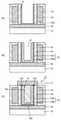
図8に示すトランジスタ11は、例えば図9に示す第1の製造工程、図10に示す第2の製造工程、図11に示す第3の製造工程、図12に示す第4の製造工程を適用することにより得ることができる。なお、下記の製造工程の例に示すように、酸化物半導体層15の第2領域R2及び第3領域R3はそれぞれ、ソース電極16と接する領域R2及びドレイン電極17と接する領域R3に設定されていてもよいし、第2領域R2及び第3領域R3のいずれか一方のみが設定されていてもよい。また、図8に示されるトランジスタ11の変形例として、前述したように円筒形状の酸化物半導体層15に代えて、内部まで酸化物半導体で構成された円柱形状の酸化物半導体層15を適用してもよい。この構造では、酸化シリコン等の絶縁膜18は充填されていない。 For the
図8に示すトランジスタ11の第1の製造工程について、図9を参照して説明する。図9に示す第1の製造工程は、ソース電極16と接する領域R2及びドレイン電極17と接する領域R3の両方にA元素の含有量を1原子%未満とした領域を設定した製造方法である。まず、図9(A)に示すように、従来の縦型トランジタと同様な工程を適用して、基板12上にソース電極16、ゲート電極13、及びゲート絶縁膜14を形成する。次に、ゲート絶縁膜14の内側に設けられる中空部Hに沿って、酸化物半導体層15の一部となるM1-M2-Oからなる第1の酸化物半導体層15Aを形成する。第1の酸化物半導体層15AはA元素を含んでおらず、第2領域R2及び第3領域R3の形成に寄与する。 The first manufacturing process of the
次に、図9(B)に示すように、第1の酸化物半導体層15A上にA元素を含むM1-M2-Oからなる第2の酸化物半導体層15Bを形成する。第2の酸化物半導体層15Bは、前述したようにA元素を所定の範囲で含んでいる。このような第1の酸化物半導体層15Aと第2の酸化物半導体層15Bとを積層して酸化物半導体層15を構成することによって、A元素の含有量が例えば傾斜的に変化した酸化物半導体層15を得ることができる。例えば、ゲート電極13と対向する第1領域R1では、第2の酸化物半導体層15Bが主として機能するため、前述した酸化物半導体層15の本来の特性を発揮させることができる。一方、ソース電極16と接する領域R2及びドレイン電極17と接する領域3には、少なくとも第1の酸化物半導体層15Aの一部が存在するため、ソース電極16やドレイン電極17とのコンタクト抵抗を低下させることができる。 Next, as shown in FIG. 9B, a second
この後、図9(C)に示すように、第2の酸化物半導体層15Bの内側に残存する中空部Hに絶縁膜18を充填した後、ドレイン電極17を形成することによって、トランジスタ11が得られる。ここで、第2の酸化物半導体層15Bの内側に残存する中空部Hに充填する絶縁膜18について、一般的にはシリコン酸化膜等が用いられる。中空部Hに充填する絶縁膜18に、例えばF及びClから選ばれる少なくとも1つのA元素を含むシリコン酸化膜を適用してもよい。絶縁膜18にFやClを含むシリコン酸化膜を適用することによって、絶縁膜18に含まれるFやClを第2の酸化物半導体層15Bに拡散させるようにしてもよい。第2の製造工程においても同様である。 After that, as shown in FIG. 9C, the
図8に示すトランジスタ11の第2の製造工程について、図10を参照して説明する。図10に示す第2の製造工程は、ソース電極16と接する第2領域R2にA元素の含有量を1原子%未満とした領域を設定した製造方法である。まず、図10(A)に示すように、図9に示す第2の製造工程と同様に、基板12上にソース電極16、ゲート電極13、及びゲート絶縁膜14を形成する。次いで、ゲート絶縁膜14の内側に設けられる中空部H内に、酸化物半導体層15の一部となるM1-M2-Oからなる第1の酸化物半導体層15Aを充填する。第1の酸化物半導体層15AはA元素を含んでおらず、第2領域R2の形成に寄与する。次いで、図10(B)に示すように、第1の酸化物半導体層15Aをエッチバックする。第1の酸化物半導体層15Aの残存部の厚さは、ソース電極16と接する第2領域R2の形成に十分な範囲であればよく、特に限定されるものではない。 The second manufacturing process of the
次に、図10(C)に示すように、第1の酸化物半導体層15A上を含む中空部H内に、A元素を含むM1-M2-Oからなる第2の酸化物半導体層15Bを形成する。第2の酸化物半導体層15Bは、前述したようにA元素を所定の範囲で含んでいる。このような第1の酸化物半導体層15Aと第2の酸化物半導体層15Bとを積層して酸化物半導体層15を構成することによって、ゲート電極13と対向する第1領域R1を第2の酸化物半導体層15Bで形成すると共に、ソース電極16と接する第2領域R2を第1の酸化物半導体層15Aで形成することができる。従って、第1領域R1に酸化物半導体層15の特性を発揮させた上で、ソース電極16とのコンタクト抵抗を低下させることができる。 Next, as shown in FIG. 10C, a second
この後、図10(D)に示すように、第2の酸化物半導体層15Bの内側に残存する中空部Hに絶縁膜18を充填した後、ドレイン電極17を形成することによって、トランジスタ11が得られる。第2の酸化物半導体層15Bの内側に残存する中空部Hに充填する絶縁膜18については、第1の製造工程で示したように、F及びClから選ばれる少なくとも1つのA元素を含むシリコン酸化膜を適用してもよい。絶縁膜18にFやClを含むシリコン酸化膜を適用することによって、絶縁膜18に含まれるFやClを第2の酸化物半導体層15Bに拡散させるようにしてもよい。 After that, as shown in FIG. 10 (D), the
図8に示すトランジスタ11の第3の製造工程について、図11を参照して説明する。図11に示す第3の製造工程は、ドレイン電極17と接する第3領域R3にA元素の含有量を1原子%未満とした領域を設定した製造方法である。まず、図11(A)に示すように、図9に示す第2の製造工程と同様に、基板12上にソース電極16、ゲート電極13、及びゲート絶縁膜14を形成する。次いで、ゲート絶縁膜14の内側に設けられる中空部H内に、A元素を含むM1-M2-Oからなる第2の酸化物半導体層15Bを充填する。次いで、図11(B)に示すように、第2の酸化物半導体層15Bをエッチバックする。第2の酸化物半導体層15Bのエッチバックの深さは、ドレイン電極17と接する第3領域R3の形成に十分な範囲であればよく、特に限定されるものではない。 The third manufacturing process of the
次に、図11(C)に示すように、第2の酸化物半導体層15Bをエッチバックして形成した中空部H内に、A元素を含まないM1-M2-Oからなる第1の酸化物半導体層15Bを形成する。このような第1の酸化物半導体層15Aと第2の酸化物半導体層15Bとを積層して酸化物半導体層15を構成することによって、ゲート電極13と隣接する第1領域R1を第2の酸化物半導体層15Bで形成すると共に、ドレイン電極17と接する第3領域R3を第1の酸化物半導体層15Aで形成することができる。従って、第1領域R1に酸化物半導体層15の特性を発揮させた上で、ドレイン電極17とのコンタクト抵抗を低下させることができる。この後、図11(D)に示すように、酸化物半導体層15上にドレイン電極17を形成することによって、トランジスタ11が得られる。 Next, as shown in FIG. 11C, the first oxidation composed of M1-M2-O containing no element A in the hollow portion H formed by etching back the second
図8に示すトランジスタ11の第4の製造工程について、図12を参照して説明する。図12に示す第4の製造工程は、第2の製造工程と第3の製造工程とを組み合わせたものである。まず、図10(B)に示した工程と同様にして、中空部H内に充填された第1の酸化物半導体層15Aをエッチバックする(図12(A))。次いで、図12(B)に示すように、第1の酸化物半導体層15A上を含む中空部H内に、A元素を含むM1-M2-Oからなる第2の酸化物半導体層15Bを充填する。 The fourth manufacturing process of the
次に、図12(C)に示すように、第2の酸化物半導体層15Bをエッチバックし、エッチバックにより形成された中空部H内に、A元素を含まないM1-M2-Oからなる第3の酸化物半導体層15Cを形成する。このような第1の酸化物半導体層15Aと第2の酸化物半導体層15Bと第3の酸化物半導体層15Cとを積層して酸化物半導体層15を構成することによって、ゲート電極13と隣接する第1領域R1を第2の酸化物半導体層15Bで形成すると共に、ソース電極16と接する第2領域R2とドレイン電極17と接する第3領域R3をそれぞれ第1及び第3の酸化物半導体層15A、15Cで形成することができる。従って、第1領域R1に酸化物半導体層15の特性を発揮させた上で、ソース電極16及びドレイン電極17とのコンタクト抵抗を低下させることができる。この後、図12(D)に示すように、酸化物半導体層15上にドレイン電極17を形成することによって、トランジスタ11が得られる。 Next, as shown in FIG. 12 (C), the second
なお、図11(D)及び図12(D)では、酸化物半導体層15を円柱状に形成した状態を示しているが、第3及び第4の製造工程では図8に示したような酸化物半導体層15を適用することもできる。酸化物半導体層15を中空部Hの内面に沿って形成することによって、図8に示したような形状を有する酸化物半導体層15を得ることができる。この場合、酸化物半導体層15の内側に形成される中空部に絶縁膜18を充填すればよい。 Although FIGS. 11 (D) and 12 (D) show a state in which the
(第3の実施形態)
図13、図14、及び図15は、第3の実施形態の半導体記憶装置を示している。これらの図に示す半導体記憶装置は、複数のメモリセルアレイを有する。図13は、メモリセルアレイの回路構成例を説明するための回路図である。図13は、複数のメモリセルMCと、複数のワード線WL(ワード線WLn、ワード線WLn+1、ワード線WLn+2、nは整数)と、複数のビット線BL(ビット線BLm、ビット線BLm+1、ビット線BLm+2、mは整数)と、を図示する。(Third embodiment)
13, 14, and 15 show the semiconductor storage device of the third embodiment. The semiconductor storage device shown in these figures has a plurality of memory cell arrays. FIG. 13 is a circuit diagram for explaining a circuit configuration example of the memory cell array. FIG. 13 shows a plurality of memory cells MC, a plurality of word line WLs (word line WLn, word
複数のメモリセルMCは、行列方向に配列され、メモリセルアレイを構成する。それぞれのメモリセルMCは、電界効果トランジスタ(FET)であるメモリトランジスタMTRと、メモリキャパシタMCPとを備える。メモリトランジスタMTRのゲートは対応するワード線WLに接続され、ソース又はドレインの一方は対応するビット線BLに接続される。メモリキャパシタMCPの一方の電極はメモリトランジスタMTRのソース又はドレインの他方に接続され、他方の電極は図示しないが特定の電位を供給する電源線に接続される。メモリセルMCは、ワード線WLによるメモリトランジスタMTRのスイッチングによりビット線BLからメモリキャパシタMCPに電荷を蓄積してデータを保持できる。複数のメモリセルMCの数は、図13に示す数に限定されない。 The plurality of memory cells MC are arranged in the matrix direction to form a memory cell array. Each memory cell MC includes a memory transistor MTR which is a field effect transistor (FET) and a memory capacitor MCP. The gate of the memory transistor MTR is connected to the corresponding word line WL and one of the source or drain is connected to the corresponding bit line BL. One electrode of the memory capacitor MCP is connected to the other of the source or drain of the memory transistor MTR, and the other electrode is connected to a power line that supplies a specific potential (not shown). The memory cell MC can store data from the bit line BL to the memory capacitor MCP by switching the memory transistor MTR by the word line WL and hold the data. The number of the plurality of memory cells MC is not limited to the number shown in FIG.
メモリセルMCにおける電界効果トランジスタMTRとメモリキャパシタMCPの構造例について、図14及び図15を参照して説明する。図14及び図15において、符号30はメモリキャパシタMCPであり、符号51は電界効果トランジスタ(メモリトランジスタ)MTRである。図14はメモリセルMCの斜視模式図、図15はメモリセルMCの断面模式図である。キャパシタ30は、半導体基板の上方及び電界効果トランジスタ51の下方に設けられ、メモリセルMCのメモリキャパシタMCPを構成する。 A structural example of the field effect transistor MTR and the memory capacitor MCP in the memory cell MC will be described with reference to FIGS. 14 and 15. In FIGS. 14 and 15,
キャパシタ30は、いわゆるピラー型キャパシタ、シリンダー型キャパシタ等の3次元キャパシタであって、図14及び図15に示すように、セル電極31と、絶縁膜32と、プレート電極33と、プレート電極34とを有する。セル電極31は、メモリキャパシタMCPの第1の電極として機能する。絶縁膜32は、メモリキャパシタMCPの誘電体層として機能し、セル電極31とプレート電極33との間に設けられる。プレート電極33は、メモリキャパシタMCPの第2の電極として機能し、セル電極31に対向して設けられる。プレート電極34は、プレート電極33に接続される。上記3次元キャパシタ30によりメモリセルMCの面積を小さくできる。 The
酸化物導電層41は、図14及び図15に示すように、セル電極31に接して設けられる。酸化物導電層41は、例えばインジウム-錫-酸化物(ITO)等の金属酸化物を含む。電界効果トランジスタ51は、半導体基板の上方及びキャパシタ30の上方に設けられ、メモリセルMCのメモリトランジスタMTRを構成する。 As shown in FIGS. 14 and 15, the oxide
電界効果トランジスタ51は、図14及び図15に示すように、金属酸化物等の酸化物半導体を含むチャネル層501と、チャネル層501を囲むゲート絶縁膜502とを有する。チャネル層501のZ軸方向の一端は、酸化物導電層42を介して配線71に接続され、電界効果トランジスタ51のソース又はドレインの一方として機能し、他方が酸化物導電層41に接続され、電界効果トランジスタ51のソース又はドレインの他方として機能する。このとき、酸化物導電層41は、キャパシタ30のセル電極31と電界効果トランジスタ51のチャネル層501との間に設けられ、電界効果トランジスタ51のソース電極又はドレイン電極の他方として機能する。酸化物導電層41は、電界効果トランジスタ51のチャネル層501と同様に金属酸化物を含むため、電界効果トランジスタ51と酸化物導電層41との接続抵抗を低減できる。 As shown in FIGS. 14 and 15, the
チャネル層501は、前述した第1及び第2の実施形態における酸化物半導体層(5、15)と同様な構成を有する。ゲート絶縁膜502は、例えば酸化物又は酸窒化物(一例として、酸化シリコン)を含む。配線61は、図14及び図15に示すように、ゲート絶縁膜502を挟んでチャネル層501に対向して設けられ、電界効果トランジスタ51のゲート電極として機能する。電界効果トランジスタ51は、図14に示すように、ゲート電極がチャネル層501を囲んで配置される、いわゆるSurrounding Gate Transistor(SGT)である。SGTにより半導体記憶装置の面積を小さくできる。 The
酸化物半導体を含むチャネル層を有する電界効果トランジスタは、半導体基板に設けられた電界効果トランジスタよりもオフリーク電流が低い。よって、例えばメモリセルMCに保持されたデータを長く保持できるため、リフレッシュ動作の回数を減らすことができる。また、酸化物半導体を含むチャネル層を有する電界効果トランジスタは、低温プロセスで形成可能であるため、キャパシタ30に熱ストレスを与えることを抑制できる。 A field-effect transistor having a channel layer containing an oxide semiconductor has a lower off-leakage current than a field-effect transistor provided on a semiconductor substrate. Therefore, for example, the data held in the memory cell MC can be held for a long time, so that the number of refresh operations can be reduced. Further, since the field effect transistor having a channel layer including an oxide semiconductor can be formed by a low temperature process, it is possible to suppress the application of thermal stress to the
配線61は、例えば金属、金属化合物、又は、半導体を含む。配線61は、例えばタングステン(W)、チタン(Ti)、窒化チタン(TiN)、モリブデン(Mo)、コバルト(Co)、及びルテニウム(Ru)からなる群より選ばれる少なくとも一つの材料を含む。 The
酸化物導電層42は、図14及び図15に示すように、電界効果トランジスタ51のチャネル層501に接して設けられ、電界効果トランジスタ51のソース電極又はドレイン電極の一方として機能する。酸化物導電層42は、例えばインジウム-錫-酸化物(ITO)等の金属酸化物を含む。酸化物導電層42は、電界効果トランジスタ51のチャネル層501と同様に金属酸化物を含むため、電界効果トランジスタ51と酸化物導電層42との接続抵抗を低減できる。 As shown in FIGS. 14 and 15, the oxide
配線71は、図14及び図15に示すように、電界効果トランジスタ51の上方において酸化物導電層42に接して設けられ、酸化物導電層42を介して電界効果トランジスタ51のチャネル層501に接続される。酸化物導電層42は、電界効果トランジスタ51のソース電極又はドレイン電極の一方として機能する。 As shown in FIGS. 14 and 15, the
本発明のいくつかの実施形態を説明したが、これらの実施形態は例として提示したものであり、発明の範囲を限定することは意図していない。これら新規な実施形態は、その他の様々な形態で実施し得るものであり、発明の要旨を逸脱しない範囲で、種々の省略、置き換え、変更を行うことができる。これら実施形態やその変形は、発明の範囲や要旨に含まれると共に、特許請求の範囲に記載された発明とその均等の範囲に含まれる。 Although some embodiments of the present invention have been described, these embodiments are presented as examples and are not intended to limit the scope of the invention. These novel embodiments can be implemented in various other embodiments, and various omissions, replacements, and changes can be made without departing from the gist of the invention. These embodiments and variations thereof are included in the scope and gist of the invention, and are also included in the scope of the invention described in the claims and the equivalent scope thereof.
1…トランジスタ、2,12…基板、3,13…第1電極、4,14…絶縁膜、5,15…酸化物半導体層、6,16…第2電極、7,17…第3電極、11…縦型トランジスタ、18…絶縁膜 1 ... Transistor, 2,12 ... Substrate, 3,13 ... First electrode, 4,14 ... Insulating film, 5,15 ... Oxide semiconductor layer, 6,16 ... Second electrode, 7,17 ... Third electrode, 11 ... Vertical transistor, 18 ... Insulation film
Claims (9)
Translated fromJapanese前記酸化物半導体層は、インジウム及び錫からなる群より選ばれる少なくとも1つの第1の金属元素と、亜鉛、ガリウム、アルミニウム、タングステン、及びケイ素からなる群より選ばれる少なくとも1つの第2の金属元素とを含む金属酸化物を備え、
前記酸化物半導体層は、前記金属酸化物に対して、フッ素及び塩素からなる群より選ばれる少なくとも1つのアニオン元素が1原子%以上8原子%未満の範囲で含有された第1領域を備える、半導体装置。A semiconductor device including an oxide semiconductor layer.
The oxide semiconductor layer has at least one first metal element selected from the group consisting of indium and tin, and at least one second metal element selected from the group consisting of zinc, gallium, aluminum, tungsten, and silicon. Equipped with metal oxides including and
The oxide semiconductor layer comprises a first region containing at least one anionic element selected from the group consisting of fluorine and chlorine in a range of 1 atomic% or more and less than 8 atomic% with respect to the metal oxide. Semiconductor equipment.
組成式:M2iM3jM4kM6l(O,F,Cl)n
(式中、M2はZn、M3はIn、Ga、及びAl、M4はSn及びSi、M6はWを表し、iはM2の原子比、jはM3の原子比、kはM4の原子比、lはM6の原子比、nはO、F、及びClの合計原子比を表す。)
で表したとき、前記第1領域は、
(2i+3j+4k+6l)/2×0.95<n<(2i+3j+4k+6l)/2×1.05
の関係を満足する組成を有する、請求項1乃至請求項3のいずれかに記載の半導体装置。The composition of the first region
Composition formula: M2i M3j M4k M6l (O, F, Cl)n
(In the formula, M2 is Zn, M3 is In, Ga, and Al, M4 is Sn and Si, M6 is W, i is the atomic ratio of M2 , j is the atomic ratio of M3 , and k. Is the atomic ratio of M4 , l is the atomic ratio of M6 , and n is the total atomic ratio of O, F, and Cl.)
When represented by, the first region is
(2i + 3j + 4k + 6l) / 2 × 0.95 <n <(2i + 3j + 4k + 6l) / 2 × 1.05
The semiconductor device according to any one of claims 1 to 3, which has a composition satisfying the above-mentioned relationship.
かつ、前記酸化物半導体層は、前記第2電極と電気的に接続する、前記金属酸化物に対して前記アニオン元素の含有量が1原子%未満の第2領域、及び前記第3電極と電気的に接続する、前記金属酸化物に対して前記アニオン元素の含有量が1原子%未満の第3領域の少なくとも一方を備える、請求項5に記載の半導体装置。The first region is provided so as to face the first electrode.
Moreover, the oxide semiconductor layer is electrically connected to the second electrode, the second region in which the content of the anion element is less than 1 atomic% with respect to the metal oxide, and electricity to the third electrode. The semiconductor device according to claim 5, further comprising at least one of a third region having an anion element content of less than 1 atomic% with respect to the metal oxide to be connected.
前記第2電極は、前記酸化物半導体層の前記第1方向の一端側と電気的に接続して設けられていると共に、前記第3電極は前記酸化物半導体層の前記第1方向の他端側に電気的に接続して設けられている、請求項5又は請求項6に記載の半導体装置。The oxide semiconductor layer is laminated on the first electrode so as to extend in the first direction via the insulating film.
The second electrode is electrically connected to one end side of the oxide semiconductor layer in the first direction, and the third electrode is the other end of the oxide semiconductor layer in the first direction. The semiconductor device according to claim 5 or 6, which is provided by being electrically connected to the side.
前記第1電極は、前記酸化物半導体層の外周面に沿って、前記絶縁膜を介して設けられ、
前記第2電極は、前記酸化物半導体層の前記第1端部と電気的に接続するように設けられ、
前記第3電極は、前記酸化物半導体層の前記第2端部と電気的に接続するように設けられている、請求項5又は請求項6に記載の半導体装置。The oxide semiconductor layer extends in the first direction and includes a first end portion and a second end portion opposite to the first end portion.
The first electrode is provided along the outer peripheral surface of the oxide semiconductor layer via the insulating film.
The second electrode is provided so as to be electrically connected to the first end portion of the oxide semiconductor layer.
The semiconductor device according to claim 5 or 6, wherein the third electrode is provided so as to be electrically connected to the second end portion of the oxide semiconductor layer.
Priority Applications (4)
| Application Number | Priority Date | Filing Date | Title |
|---|---|---|---|
| JP2020142583AJP2022038209A (en) | 2020-08-26 | 2020-08-26 | Semiconductor device |
| TW110100279ATWI758052B (en) | 2020-08-26 | 2021-01-05 | semiconductor device |
| CN202110108855.6ACN114122140B (en) | 2020-08-26 | 2021-01-27 | semiconductor devices |
| US17/193,941US11569241B2 (en) | 2020-08-26 | 2021-03-05 | Semiconductor device |
Applications Claiming Priority (1)
| Application Number | Priority Date | Filing Date | Title |
|---|---|---|---|
| JP2020142583AJP2022038209A (en) | 2020-08-26 | 2020-08-26 | Semiconductor device |
Publications (1)
| Publication Number | Publication Date |
|---|---|
| JP2022038209Atrue JP2022038209A (en) | 2022-03-10 |
Family
ID=80357371
Family Applications (1)
| Application Number | Title | Priority Date | Filing Date |
|---|---|---|---|
| JP2020142583APendingJP2022038209A (en) | 2020-08-26 | 2020-08-26 | Semiconductor device |
Country Status (4)
| Country | Link |
|---|---|
| US (1) | US11569241B2 (en) |
| JP (1) | JP2022038209A (en) |
| CN (1) | CN114122140B (en) |
| TW (1) | TWI758052B (en) |
Families Citing this family (6)
| Publication number | Priority date | Publication date | Assignee | Title |
|---|---|---|---|---|
| US11322442B2 (en) | 2018-01-05 | 2022-05-03 | Semiconductor Energy Laboratory Co., Ltd. | Semiconductor device including transistor with oxide semiconductor and method for manufacturing the semiconductor device |
| US11374057B2 (en)* | 2020-06-23 | 2022-06-28 | Taiwan Semiconductor Manufacturing Company Limited | Vertical metal oxide semiconductor channel selector transistor and methods of forming the same |
| JP2022143580A (en) | 2021-03-17 | 2022-10-03 | キオクシア株式会社 | Semiconductor device and semiconductor memory device |
| US12426250B2 (en) | 2022-06-21 | 2025-09-23 | Changxin Memory Technologies, Inc. | Semiconductor structure, method for manufacturing same and memory |
| CN117320439A (en)* | 2022-06-21 | 2023-12-29 | 长鑫存储技术有限公司 | Semiconductor structure, manufacturing method thereof and memory |
| US20240349485A1 (en)* | 2023-04-11 | 2024-10-17 | Nanya Technology Corporation | Semiconductor structure and method of manufacturing the same |
Family Cites Families (10)
| Publication number | Priority date | Publication date | Assignee | Title |
|---|---|---|---|---|
| US7700984B2 (en)* | 2005-05-20 | 2010-04-20 | Semiconductor Energy Laboratory Co., Ltd | Semiconductor device including memory cell |
| TWI491048B (en) | 2008-07-31 | 2015-07-01 | Semiconductor Energy Lab | Semiconductor device |
| TWI567829B (en)* | 2008-10-31 | 2017-01-21 | 半導體能源研究所股份有限公司 | Semiconductor device and method of manufacturing same |
| EP2486594B1 (en)* | 2009-10-08 | 2017-10-25 | Semiconductor Energy Laboratory Co., Ltd. | Oxide semiconductor device |
| KR101291488B1 (en) | 2009-10-21 | 2013-07-31 | 가부시키가이샤 한도오따이 에네루기 켄큐쇼 | Semiconductor device |
| KR102114012B1 (en) | 2010-03-05 | 2020-05-22 | 가부시키가이샤 한도오따이 에네루기 켄큐쇼 | Display device |
| JP6220526B2 (en) | 2012-02-29 | 2017-10-25 | 株式会社半導体エネルギー研究所 | Method for manufacturing semiconductor device |
| WO2014021442A1 (en)* | 2012-08-03 | 2014-02-06 | Semiconductor Energy Laboratory Co., Ltd. | Oxide semiconductor stacked film and semiconductor device |
| US10651252B2 (en) | 2014-03-26 | 2020-05-12 | International Business Machines Corporation | Vertically integrated active matrix backplane |
| KR20160137843A (en)* | 2015-05-22 | 2016-12-01 | 엘지디스플레이 주식회사 | Thin Film Transistor Substrate Having High Reliability Metal Oxide Semiconductor Material |
- 2020
- 2020-08-26JPJP2020142583Apatent/JP2022038209A/enactivePending
- 2021
- 2021-01-05TWTW110100279Apatent/TWI758052B/enactive
- 2021-01-27CNCN202110108855.6Apatent/CN114122140B/enactiveActive
- 2021-03-05USUS17/193,941patent/US11569241B2/enactiveActive
Also Published As
| Publication number | Publication date |
|---|---|
| TWI758052B (en) | 2022-03-11 |
| TW202209686A (en) | 2022-03-01 |
| US20220068925A1 (en) | 2022-03-03 |
| US11569241B2 (en) | 2023-01-31 |
| CN114122140B (en) | 2025-08-29 |
| CN114122140A (en) | 2022-03-01 |
Similar Documents
| Publication | Publication Date | Title |
|---|---|---|
| TWI758052B (en) | semiconductor device | |
| US11800823B2 (en) | Method for manufacturing thermal dispersion layer in programmable metallization cell | |
| JP2020198343A (en) | Semiconductor device and semiconductor memory device | |
| JP2019169490A (en) | Semiconductor device and manufacturing method thereof | |
| US20240113223A1 (en) | Semiconductor devices comprising transistors having increased threshold voltage and related methods and systems | |
| JP2022143580A (en) | Semiconductor device and semiconductor memory device | |
| KR20190006143A (en) | Semiconductor device including capacitor | |
| KR102861948B1 (en) | Semiconductor device | |
| US12439699B2 (en) | Semiconductor memory device | |
| JP2022049604A (en) | Semiconductor devices and semiconductor storage devices | |
| JP7387475B2 (en) | Semiconductor devices and semiconductor storage devices | |
| US20210066303A1 (en) | Semiconductor device and method for fabricating the same | |
| US20240015950A1 (en) | Semiconductor device and method for manufacturing semiconductor device | |
| TWI830322B (en) | Semiconductor devices and semiconductor memory devices | |
| US20230035006A1 (en) | Semiconductor memory device | |
| TW202401757A (en) | Semiconductor device and semiconductor memory device | |
| CN115835623B (en) | semiconductor memory devices | |
| US20230422482A1 (en) | Semiconductor device and semiconductor memory device | |
| US20240421232A1 (en) | Semiconductor device | |
| US20250220872A1 (en) | Semiconductor device | |
| US20240098962A1 (en) | Semiconductor device and semiconductor memory device | |
| JP2024000621A (en) | Semiconductor device and semiconductor memory device | |
| JP2024000648A (en) | Semiconductor device and semiconductor memory device | |
| KR20250144336A (en) | Semiconductor device | |
| KR20240156156A (en) | Semiconductor device |