JP2022037046A - Semiconductor device - Google Patents
Semiconductor deviceDownload PDFInfo
- Publication number
- JP2022037046A JP2022037046AJP2021197272AJP2021197272AJP2022037046AJP 2022037046 AJP2022037046 AJP 2022037046AJP 2021197272 AJP2021197272 AJP 2021197272AJP 2021197272 AJP2021197272 AJP 2021197272AJP 2022037046 AJP2022037046 AJP 2022037046A
- Authority
- JP
- Japan
- Prior art keywords
- potential
- capacitive element
- channel transistor
- electrode
- power supply
- Prior art date
- Legal status (The legal status is an assumption and is not a legal conclusion. Google has not performed a legal analysis and makes no representation as to the accuracy of the status listed.)
- Withdrawn
Links
- 239000004065semiconductorSubstances0.000titleclaimsabstractdescription33
- 239000012535impuritySubstances0.000description13
- 239000010408filmSubstances0.000description10
- 230000007257malfunctionEffects0.000description7
- ORQBXQOJMQIAOY-UHFFFAOYSA-NnobeliumChemical compound[No]ORQBXQOJMQIAOY-UHFFFAOYSA-N0.000description7
- 239000000758substrateSubstances0.000description6
- 230000000717retained effectEffects0.000description5
- 238000009825accumulationMethods0.000description4
- 238000006243chemical reactionMethods0.000description4
- CNQCVBJFEGMYDW-UHFFFAOYSA-Nlawrencium atomChemical compound[Lr]CNQCVBJFEGMYDW-UHFFFAOYSA-N0.000description4
- 229910021417amorphous siliconInorganic materials0.000description3
- 238000010586diagramMethods0.000description3
- OKTJSMMVPCPJKN-UHFFFAOYSA-NCarbonChemical compound[C]OKTJSMMVPCPJKN-UHFFFAOYSA-N0.000description2
- 230000005540biological transmissionEffects0.000description2
- 239000002041carbon nanotubeSubstances0.000description2
- 229910021393carbon nanotubeInorganic materials0.000description2
- 239000013078crystalSubstances0.000description2
- 238000007599dischargingMethods0.000description2
- 238000000034methodMethods0.000description2
- 229910021420polycrystalline siliconInorganic materials0.000description2
- 238000005070samplingMethods0.000description2
- 239000010409thin filmSubstances0.000description2
- 101000800735Mycolicibacterium fortuitum Putative 3-methyladenine DNA glycosylaseProteins0.000description1
- XUIMIQQOPSSXEZ-UHFFFAOYSA-NSiliconChemical compound[Si]XUIMIQQOPSSXEZ-UHFFFAOYSA-N0.000description1
- 230000002411adverseEffects0.000description1
- 239000003990capacitorSubstances0.000description1
- 230000003247decreasing effectEffects0.000description1
- 230000000694effectsEffects0.000description1
- 239000011521glassSubstances0.000description1
- 239000011229interlayerSubstances0.000description1
- 239000004973liquid crystal related substanceSubstances0.000description1
- 239000013081microcrystalSubstances0.000description1
- 229910021421monocrystalline siliconInorganic materials0.000description1
- 238000010606normalizationMethods0.000description1
- 229910052710siliconInorganic materials0.000description1
- 239000010703siliconSubstances0.000description1
Images


Classifications
- H—ELECTRICITY
- H03—ELECTRONIC CIRCUITRY
- H03K—PULSE TECHNIQUE
- H03K19/00—Logic circuits, i.e. having at least two inputs acting on one output; Inverting circuits
- H03K19/01—Modifications for accelerating switching
- H03K19/017—Modifications for accelerating switching in field-effect transistor circuits
- H03K19/01728—Modifications for accelerating switching in field-effect transistor circuits in synchronous circuits, i.e. by using clock signals
- G—PHYSICS
- G11—INFORMATION STORAGE
- G11C—STATIC STORES
- G11C7/00—Arrangements for writing information into, or reading information out from, a digital store
- H—ELECTRICITY
- H03—ELECTRONIC CIRCUITRY
- H03K—PULSE TECHNIQUE
- H03K19/00—Logic circuits, i.e. having at least two inputs acting on one output; Inverting circuits
- H03K19/0175—Coupling arrangements; Interface arrangements
- H03K19/0185—Coupling arrangements; Interface arrangements using field effect transistors only
- H03K19/018507—Interface arrangements
- H03K19/01855—Interface arrangements synchronous, i.e. using clock signals
Landscapes
- Engineering & Computer Science (AREA)
- Computer Hardware Design (AREA)
- Physics & Mathematics (AREA)
- Computing Systems (AREA)
- General Engineering & Computer Science (AREA)
- Mathematical Physics (AREA)
- Logic Circuits (AREA)
- Control Of Indicators Other Than Cathode Ray Tubes (AREA)
- Electronic Switches (AREA)
- Liquid Crystal Display Device Control (AREA)
- Metal-Oxide And Bipolar Metal-Oxide Semiconductor Integrated Circuits (AREA)
- Semiconductor Integrated Circuits (AREA)
- Devices For Indicating Variable Information By Combining Individual Elements (AREA)
Abstract
Description
Translated fromJapanese 本発明はデジタル信号によって動作するデジタル回路に関し、さらに該デジタル回路を
1つまたは複数有する半導体装置、電子機器及びその駆動方法に関する。The present invention relates to a digital circuit operated by a digital signal, and further relates to a semiconductor device having one or a plurality of the digital circuits, an electronic device, and a method for driving the same.
デジタル信号を処理する論理回路(以下、デジタル回路と呼ぶ)は、基本単位となる論
理素子が単独で、または複数組み合わされて構成されている。論理素子は単数または複数
の入力に対して一の出力が得られる回路であり、例えばインバータ、AND、OR、NO
T、NAND、NOR、クロックドインバータ、トランスミッションゲート等がこれに相
当する。A logic circuit that processes a digital signal (hereinafter referred to as a digital circuit) is configured by a single logic element or a combination of a plurality of logic elements as a basic unit. A logic element is a circuit that can obtain one output for one or more inputs, such as an inverter, AND, OR, NO.
T, NAND, NOR, clocked inverter, transmission gate, etc. correspond to this.
論理素子は、トランジスタ、抵抗、コンデンサ等の単数または複数の回路素子が接続さ
れて構成されている。そして、論理素子に入力されたデジタル信号に従って該複数の各回
路素子が動作することにより、後段の回路へ供給される信号の電位又は電流が制御される
。A logic element is configured by connecting a single or a plurality of circuit elements such as transistors, resistors, and capacitors. Then, by operating each of the plurality of circuit elements according to the digital signal input to the logic element, the potential or current of the signal supplied to the subsequent circuit is controlled.
論理素子の1つであるインバータを例に挙げ、その構成と動作について具体的に説明す
る。Taking an inverter, which is one of the logic elements, as an example, its configuration and operation will be specifically described.
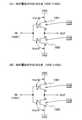
図13(A)に一般的なインバータの回路図を示す。図13(A)においてINは入力
される信号(入力信号)を意味し、OUTは出力される信号(出力信号)を意味している
。またVDD、VSSは電源電位を意味しており、VDD>VSSとする。FIG. 13A shows a circuit diagram of a general inverter. In FIG. 13A, IN means an input signal (input signal), and OUT means an output signal (output signal). Further, VDD and VSS mean the power supply potential, and VDD> VSS.
図13(A)に示すインバータは、pチャネル型トランジスタ1301とnチャネル型
トランジスタ1302とを有している。pチャネル型トランジスタ1301のゲート(G
)とnチャネル型トランジスタ1302のゲートは互いに接続されており、該2つのゲー
トに入力信号INが入力されている。そして、pチャネル型トランジスタ1301の第1
の端子にはVDDが与えられており、nチャネル型トランジスタ1302の第1の端子に
はVSSが与えられている。またpチャネル型トランジスタ1301の第2の端子とnチ
ャネル型トランジスタ1302の第2の端子は互いに接続されており、該2つの第2の端
子から後段の回路へ出力信号OUTが出力される。The inverter shown in FIG. 13A has a p-
) And the gates of the n-
VDD is given to the terminal of, and VSS is given to the first terminal of the n-
なお、第1の端子と第2の端子は、いずれか一方がソース、他方がドレインに相当する
。pチャネル型トランジスタの場合電位の高いほうがソース、低いほうがドレインとなる
。またnチャネル型トランジスタは電位の低いほうがソース、高いほうがドレインとなる
。よって図13(A)では2つのTFTにおいて、第1の端子がソース(S)、第2の端
子がドレイン(D)に相当する。One of the first terminal and the second terminal corresponds to the source and the other corresponds to the drain. In the case of a p-channel transistor, the one with a high potential is the source and the one with a low potential is the drain. Further, in the n-channel transistor, the lower potential is the source and the higher potential is the drain. Therefore, in FIG. 13A, in the two TFTs, the first terminal corresponds to the source (S) and the second terminal corresponds to the drain (D).
一般的に入力信号には、2値の電位を有するデジタル信号を用いる。該入力信号INの
電位に従ってインバータが有する2つの回路素子が動作し、出力信号OUTの電位が制御
される。Generally, a digital signal having a binary potential is used as an input signal. The two circuit elements of the inverter operate according to the potential of the input signal IN, and the potential of the output signal OUT is controlled.
次に、図13(B)、図13(C)を用いて、図13(A)に示したインバータの動作
について説明する。なお図13(B)、図13(C)では、動作の状態を分かり易くする
ために各回路素子を単なるスイッチとして表示した。Next, the operation of the inverter shown in FIG. 13 (A) will be described with reference to FIGS. 13 (B) and 13 (C). In FIGS. 13 (B) and 13 (C), each circuit element is displayed as a mere switch in order to make it easy to understand the state of operation.
図13(B)に、入力信号INが高電位側の電位を有するときの、各回路素子の動作の
様子を示す。ここでは、入力信号INが有する高電位側の電位をVDD’(VDD’≧V
DD)とし、説明を簡単にするためにnチャネル型トランジスタ1302の閾値電圧VTH
N≧0、pチャネル型トランジスタ1301の閾値電圧VTHP≦0と仮定する。FIG. 13B shows the operation of each circuit element when the input signal IN has a potential on the high potential side. Here, the potential on the high potential side of the input signal IN is defined as VDD'( VDD' ≧ V).
DD), and the threshold voltage VTH of the n-
It is assumed thatN ≧ 0 and the threshold voltage VTHP ≦ 0 of the p-
電位VDD’がpチャネル型トランジスタ1301のゲートに与えられると、VDD’
≧VDDであるのでゲート電圧はVGS≧0となり、pチャネル型トランジスタ1301は
オフする。なおゲート電圧とは、ゲートの電位からソースの電位を差し引いた電圧に相当
する。When the potential VDD'is applied to the gate of the p-
Since ≧ VDD, the gate voltage becomes VGS ≧ 0, and the p-
またVDD’がnチャネル型トランジスタ1302のゲートに与えられると、VDD’
>VSSであるのでゲート電圧はVGS>0となり、nチャネル型トランジスタ1302は
オンする。よって電源電位VSSが出力信号OUTの電位として後段の回路に供給される
。When VDD'is given to the gate of the n-
Since> VSS, the gate voltage becomes VGS > 0, and the n-
次に図13(C)に、入力信号INが低電位側の電位を有するときの、各回路素子の動
作の様子を示す。ここでは、入力信号INが有する低電位側の電位をVSS’(VSS’
≦VSS)とし、説明を簡単にするためにnチャネル型トランジスタ1302の閾値電圧
VTHN≧0、pチャネル型トランジスタ1301の閾値電圧VTHP≦0であると仮定する。Next, FIG. 13C shows the operation of each circuit element when the input signal IN has a potential on the low potential side. Here, the potential on the low potential side of the input signal IN is called VSS'(VSS').
≤ VSS), and for the sake of simplicity, it is assumed that the threshold voltage VTHN ≥ 0 of the n-
VSS’がnチャネル型トランジスタ1302のゲートに与えられると、VSS’≦V
SSであるのでゲート電圧はVGS≦0となり、nチャネル型トランジスタ1302はオフ
する。When VSS'is given to the gate of the n-
Since it is SS, the gate voltage becomes VGS ≤ 0, and the n-
また電位VSS’がpチャネル型トランジスタ1301のゲートに与えられると、VS
S’<VDDであるのでゲート電圧はVGS<0となり、pチャネル型トランジスタ130
1はオンする。よって電源電位VDDが出力信号OUTの電位として後段の回路に供給さ
れる。When the potential VSS'is applied to the gate of the p-
Since S'< VDD, the gate voltage is VGS <0, and the p-
1 turns on. Therefore, the power supply potential VDD is supplied to the subsequent circuit as the potential of the output signal OUT.
このように、入力信号INの電位に従って各回路素子が動作し、出力信号OUTの電位
が制御される。In this way, each circuit element operates according to the potential of the input signal IN, and the potential of the output signal OUT is controlled.
図13(B)、図13(C)を用いて説明したインバータの動作は、入力信号INの有
する2値の電位VDD’、VSS’が、それぞれVDD’≧VDD、VSS’≦VSSと
仮定した場合のものである。ここで入力信号INの有する2値の電位VDD’、VSS’
が、それぞれVDD’<VDD、VSS’>VSSと仮定したときの、図13(A)に示
したインバータの動作について検証する。ただしVSS’<VDD’とする。In the operation of the inverter described with reference to FIGS. 13 (B) and 13 (C), it is assumed that the binary potentials VDD'and VSS' possessed by the input signal IN are VDD'≧ VDD and VSS'≦ VSS, respectively. It is a case. Here, the binary potentials VDD'and VSS' possessed by the input signal IN
Will verify the operation of the inverter shown in FIG. 13 (A) when it is assumed that VDD'< VDD and VSS'> VSS, respectively. However, VSS'<VDD' is set.
まず図14(A)に、入力信号INが高電位側の電位VDD’(VDD’<VDD)を
有するときの、各回路素子の動作の様子を示す。ここでは説明を簡単にするため、nチャ
ネル型トランジスタ1302の閾値電圧VTHN≧0、pチャネル型トランジスタ1301
の閾値電圧VTHP≦0であると仮定する。First, FIG. 14A shows the operation of each circuit element when the input signal IN has the potential VDD'( VDD'<VDD) on the high potential side. Here, for the sake of simplicity, the threshold voltage VTHN ≧ 0 of the n-
It is assumed that the threshold voltage VTHP ≤ 0 of.
電位VDD’がpチャネル型トランジスタ1301のゲートに与えられると、VDD’
<VDDであるのでゲート電圧はVGS<0となる。よって、|VGS|>|VTHP|のとき
は、pチャネル型トランジスタ1301はオンする。またVDD’がnチャネル型トラン
ジスタ1302のゲートに与えられると、VDD’>VSSであるのでゲート電圧はVGS
>0となり、nチャネル型トランジスタ1302はオンする。When the potential VDD'is applied to the gate of the p-
Since <VDD, the gate voltage is VGS <0. Therefore, when | VGS |> | VTHP |, the p-
> 0, and the n-
よってpチャネル型トランジスタ1301とnチャネル型トランジスタ1302が共に
オンになるので、図13(B)に示した場合とは異なり、入力信号が高電位側の電位を有
していても、出力信号OUTの電位がVSSとはならない。Therefore, since both the p-
出力信号OUTの電位は、各々のトランジスタに流れる電流によって定まる。図14(
A)では、nチャネル型トランジスタ1302のVGSをVGSnとし、pチャネル型トラン
ジスタ1301のVGSをVGSpとすると、|VGSn|>|VGSp|なので、各々のトランジ
スタの特性やチャネル幅Wとチャネル長Lの比に差異がなければ、出力信号OUTの電位
はVDDよりもVSSに近くなる。しかし、各TFTの移動度、閾値電圧、チャネル幅と
チャネル長の比などによっては、出力信号OUTの電位がVSSよりもVDDに近い電位
となることがある。この場合、当該デジタル回路の動作は正常とは言えず、誤作動する可
能性が高い。そしてこれは連鎖的に、後段に設けられたデジタル回路の誤動作の原因とも
なりうる。The potential of the output signal OUT is determined by the current flowing through each transistor. FIG. 14 (
In A), if the VGS of the n-
また図14(B)に、入力信号INが低電位側の電位VSS’(VSS’>VSS)を
有するときの、各回路素子の動作の様子を示す。ここでは説明を簡単にするため、nチャ
ネル型トランジスタの閾値電圧VTHN≧0、pチャネル型トランジスタの閾値電圧VTHP≦
0であると仮定する。Further, FIG. 14B shows the operation of each circuit element when the input signal IN has the potential VSS'(VSS'> VSS) on the low potential side. Here, for the sake of simplicity, the threshold voltage VTHN ≧ 0 of the n-channel transistor and the threshold voltage VTHP ≦ of the p-channel transistor
It is assumed to be 0.
VSS’がnチャネル型トランジスタ1302のゲートに与えられると、VSS’>V
SSであるのでゲート電圧はVGS>0となる。よって、|VGS|>|VTHn|のときは、
nチャネル型トランジスタ1302はオンする。また電位VSS’がpチャネル型トラン
ジスタ1301のゲートに与えられると、VSS’<VDDであるのでゲート電圧はVGS
<0となり、pチャネル型トランジスタ1301はオンする。When VSS'is given to the gate of n-
Since it is SS, the gate voltage is VGS > 0. Therefore, when | VGS |> | VTHn |
The n-
<0, and the p-
よってVSS、VSS’、VTHnの値によっては、pチャネル型トランジスタ1301
とnチャネル型トランジスタ1302が共にオンになるので、図13(C)に示した場合
とは異なり、入力信号が低電位側の電位を有していても、出力信号OUTの電位がVDD
とはならない。Therefore, depending on the values of VSS, VSS', and VTHn , the p-
And the n-
It does not become.
出力信号OUTの電位は、各々のトランジスタに流れる電流によって定まる。図14(
B)では、nチャネル型トランジスタのVGSをVGSnとし、pチャネル型トランジスタの
VGSをVGSpとすると、|VGSn|<|VGSp|なので、各々のトランジスタの特性やチャ
ネル幅Wとチャネル長Lの比に差異がなければ、出力信号OUTの電位はVSSよりもV
DDに近くなる。しかし、各TFTの移動度、閾値電圧、チャネル幅とチャネル長の比な
どによっては、出力信号OUTの電位がVDDよりもVSSに近い電位となることがある
。この場合、当該デジタル回路の動作は正常とは言えず、誤作動する可能性が高い。そし
てこれは連鎖的に、後段に設けられたデジタル回路の誤動作の原因ともなりうる。The potential of the output signal OUT is determined by the current flowing through each transistor. FIG. 14 (
In B), if the VGS of the n-channel transistor is VGSn and the VGS of the p-channel transistor is VGSp , then | VGSn | << | VGSp | If there is no difference in the ratio of channel length L, the potential of the output signal OUT is V rather than VSS.
It will be closer to DD. However, depending on the mobility of each TFT, the threshold voltage, the ratio of the channel width to the channel length, and the like, the potential of the output signal OUT may be closer to VSS than VDD. In this case, the operation of the digital circuit is not normal, and there is a high possibility that it will malfunction. And this can also cause a malfunction of the digital circuit provided in the subsequent stage in a chain reaction.
このように、図13(A)に示したインバータでは、入力信号INの有する2値の電位
VDD’、VSS’が、それぞれVDD’≧VDD、VSS’≦VSSであるときに、所
望の電位を有する出力信号OUTが得られ、インバータが正常に動作するといえる。しか
し入力信号INの有する2値の電位VDD’、VSS’が、それぞれVDD’<VDD、
VSS’>VSSだと、所望の電位を有する出力信号OUTが得られず、インバータは正
常に動作しない場合がある。As described above, in the inverter shown in FIG. 13A, when the binary potentials VDD'and VSS' possessed by the input signal IN are VDD'≧ VDD and VSS'≦ VSS, respectively, a desired potential is obtained. It can be said that the output signal OUT is obtained and the inverter operates normally. However, the binary potentials VDD'and VSS' possessed by the input signal IN are VDD'< VDD, respectively.
If VSS'> VSS, the output signal OUT having a desired potential cannot be obtained, and the inverter may not operate normally.
これはインバータに限らず、他のデジタル回路についてもあてはまる。つまり、入力信
号が有する2値の電位が所定の範囲から外れていると、デジタル回路が有する回路素子が
誤作動するため、所望の電位を有する出力信号OUTが得られなくなり、該デジタル回路
が正常に動作しない。This applies not only to inverters but also to other digital circuits. That is, if the binary potential of the input signal is out of the predetermined range, the circuit element of the digital circuit malfunctions, so that the output signal OUT having the desired potential cannot be obtained, and the digital circuit is normal. Does not work.
前段の回路または配線から供給される入力信号の電位は、必ずしも当該デジタル回路が
正常に動作するような高さであるとは限らない。この場合、レベルシフタで入力信号の電
位を調整することで、デジタル回路の正常な動作を確保することが可能である。しかし一
般的にレベルシフタは、レベルシフタ内において1つの回路素子が動作することで初めて
他の回路素子が動作するというように、回路素子どうしが連動して動作するため、出力信
号の電位の立下りまたは立ち上がりが遅く、半導体装置の高速動作を妨げる原因になりが
ちである。The potential of the input signal supplied from the circuit or wiring in the previous stage is not always high enough to operate the digital circuit normally. In this case, it is possible to ensure the normal operation of the digital circuit by adjusting the potential of the input signal with the level shifter. However, in general, in the level shifter, the circuit elements operate in conjunction with each other, such that the other circuit elements operate only when one circuit element operates in the level shifter. Therefore, the potential of the output signal falls or falls. The rise is slow, and it tends to hinder the high-speed operation of semiconductor devices.
また、電源電圧が小さいと電流が少なくオンしにくいため、高速に動作させにくく、逆
に高速に動作させるために電源電圧を大きくすると消費電力が嵩んでしまうという問題が
あった。Further, when the power supply voltage is small, the current is small and it is difficult to turn on, so that it is difficult to operate at high speed. On the contrary, when the power supply voltage is increased in order to operate at high speed, there is a problem that power consumption increases.
さらに、nチャネル型トランジスタ1302とpチャネル型トランジスタ1301が同
時にオンしてショート電流が流れることから、消費電流が増大するという問題も生じる。Further, since the n-
上述したような問題を解決するため、第1の入力用インバータと第2の出力用インバー
タとを有するレベルシフタ回路において、容量(容量素子)とバイアス手段とによって第
1のインバータから第2のインバータへ入力される信号のDCレベルを変換することが提
案されている。(特許文献1参照)。しかしながらこの回路では、第2のインバータを構
成する各トランジスタのゲートと第1のインバータの出力との間に接続されているDCレ
ベル変換用容量はバイアス手段によって常にハイレベル電源電位またはローレベル電源電
位に接続されていることから、これら容量の充放電が回路の動特性に悪影響を与えたり(
すなわち回路動作速度の低下を招いたり)、或いは、これら容量の充放電に伴う電力消費
が無視できない程度に大きくなったりするという問題が生じる。また、トランジスタの閾
値にばらつきがあるような場合、各容量の静電容量を対応するトランジスタに合わせるこ
とは困難であり、そのためにDCレベル変換容量の両端の電圧が対応するトランジスタの
閾値に整合せず、トランジスタのオン・オフを正確に行なうことができないという問題も
発生し得る。In order to solve the above-mentioned problems, in a level shifter circuit having a first input inverter and a second output inverter, from the first inverter to the second inverter by means of a capacitance (capacitive element) and a bias means. It has been proposed to convert the DC level of the input signal. (See Patent Document 1). However, in this circuit, the DC level conversion capacitance connected between the gate of each transistor constituting the second inverter and the output of the first inverter is always a high level power supply potential or a low level power supply potential by the bias means. Since it is connected to, the charging and discharging of these capacities adversely affects the dynamic characteristics of the circuit (
That is, the circuit operating speed is lowered), or the power consumption associated with the charging and discharging of these capacities becomes so large that it cannot be ignored. Further, when the threshold value of the transistor varies, it is difficult to match the capacitance of each capacitance with the corresponding transistor. Therefore, the voltage across the DC level conversion capacitance is matched with the threshold value of the corresponding transistor. However, there may be a problem that the transistor cannot be turned on and off accurately.
上述した問題に鑑み、本発明では入力信号が有する2値の電位に関わらず、正常に動作
させることが可能なデジタル回路の提案を課題とする。In view of the above-mentioned problems, it is an object of the present invention to propose a digital circuit capable of operating normally regardless of the binary potential of the input signal.
本発明は、デジタル回路に実際に入力される信号の電位と、該デジタル回路を正常に動
作させ得る電位との間の電位差を予め記憶しておき、実際に入力された信号に該電位差を
加算してから各回路素子に入力する補正手段を当該デジタル回路に設けることで、デジタ
ル回路を正常に動作させるものである。The present invention stores in advance the potential difference between the potential of the signal actually input to the digital circuit and the potential at which the digital circuit can operate normally, and adds the potential difference to the actually input signal. Then, by providing the correction means for inputting to each circuit element in the digital circuit, the digital circuit can be operated normally.
その補正手段により、入力信号の低電位側の電位が供給されたときにnチャネル型トラ
ンジスタをオフさせ、入力信号の高電位側の電位が供給されたときにpチャネル型トラン
ジスタをオフさせることができる。その結果、デジタル回路を正常に動作させることがで
きる。By the correction means, the n-channel transistor can be turned off when the potential on the low potential side of the input signal is supplied, and the p-channel transistor can be turned off when the potential on the high potential side of the input signal is supplied. can. As a result, the digital circuit can be operated normally.
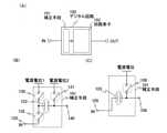
図1(A)に本発明のデジタル回路の構成を示す。デジタル回路100は、入力された
信号INの電位を補正する補正手段101と、該補正手段101によって補正された入力
信号によって動作が制御される1つまたは複数の回路素子102を有している。そして該
回路素子の動作に従って出力信号OUTの電位が制御される。FIG. 1A shows the configuration of the digital circuit of the present invention. The
図1(B)に、本発明のデジタル回路が有する補正手段101の第1の構成を簡単に示
す。第1の構成の補正手段101は、入力信号の高電位側または低電位側のいずれか一方
の電位を補正するための容量素子123を有する。FIG. 1B briefly shows the first configuration of the correction means 101 included in the digital circuit of the present invention. The correction means 101 of the first configuration includes a
そして、容量素子123の第1の電極への電源電位1の供給を制御するスイッチ130
と、容量素子123の第2の電極への電源電位2の供給を制御するスイッチ131とを有
する。また、容量素子123の第1の電極への入力信号INの電位の供給を制御するスイ
ッチ132が設けられている。そして、容量素子123の第2の電極は出力端子140に
接続されている。Then, the
And a
なお、入力信号INの高電位側の電位を補正する場合、電源電位1≦電源電位2とする
。また、入力信号INの低電位側の電位を補正する場合、電源電位1≧電源電位2である
。When correcting the potential on the high potential side of the input signal IN, the power supply potential 1 ≦ the power supply potential 2. Further, when correcting the potential on the low potential side of the input signal IN, the power supply potential 1 ≧ power supply potential 2.
そしてスイッチ130、131を制御することで、容量素子123に電源電位1と電源
電位2の電位差を記憶、保持させることができる。Then, by controlling the
そしてスイッチ132を制御することで、入力信号INの電位が容量素子123の第1
の電極に与えられると、入力信号INの電位に容量素子123に保持されている電位差が
加算されて、後段の回路素子102に入力される。Then, by controlling the
When given to the electrode of, the potential difference held in the
よって、電源電位1と電源電位2の電位差を所望の大きさに制御することで、回路素子
102に与えられる電位の高さを制御することができ、回路素子102ひいてはデジタル
回路100を正常に動作させることができる。Therefore, by controlling the potential difference between the power supply potential 1 and the power supply potential 2 to a desired magnitude, the height of the potential given to the
正常な動作とは、入力信号INが低電圧側の電位のときの、出力端子の電位が、入力信
号INがVSSと等しいときの出力端子の電位とほぼ等しい状態にあり、入力信号INが
高電位側の電位のときの出力端子の電位が、入力信号INがVDDのときの出力とほぼ等
しい状態にある場合のことを言う。なお、必ずしも出力がVSSやVDDに等しくなくて
も、後段に設けられたデジタル回路が誤動作しなければ正常な動作をしていると見なすこ
とができる。Normal operation means that the potential of the output terminal when the potential of the input signal IN is on the low voltage side is almost equal to the potential of the output terminal when the potential of the input signal IN is equal to VSS, and the potential of the input signal IN is high. This refers to the case where the potential of the output terminal when the potential on the potential side is the potential is almost equal to the output when the input signal IN is VDD. Even if the output is not necessarily equal to VSS or VDD, it can be considered that the digital circuit provided in the subsequent stage is operating normally if it does not malfunction.
図1(C)に、本発明のデジタル回路が有する補正手段101の第2の構成を簡単に示
す。第2の構成の補正手段101は、図1(B)の電源電位1を入力信号の電位で代用し
て補正を行なうものに相当する。具体的に第2の構成の補正手段101は、入力信号IN
の電位を補正するための容量素子103を有する。FIG. 1C briefly shows the second configuration of the correction means 101 included in the digital circuit of the present invention. The correction means 101 having the second configuration corresponds to one that performs correction by substituting the potential of the power supply potential 1 in FIG. 1B with the potential of the input signal. Specifically, the correction means 101 having the second configuration is an input signal IN.
It has a
なお、入力信号INの高電位側の電位を補正する場合、入力信号INの高電位側の電位
≦電源電位とする。また、入力信号INの低電位側の電位を補正する場合、入力信号IN
の低電位側の電位≧電源電位である。When correcting the potential on the high potential side of the input signal IN, the potential on the high potential side of the input signal IN ≤ the power supply potential. When correcting the potential on the low potential side of the input signal IN, the input signal IN
The potential on the low potential side of the above ≥ the power supply potential.
容量素子103には、入力信号INの高電位側または低電位側のいずれか一方の電位と
、電源電位との間の電位差を予め記憶させておく。電源電位の容量素子103への供給は
、スイッチ108で制御する。The
上記構成により、入力信号INの電位に容量素子103に保持されている電位差が加算
されて後段の回路素子102に入力される。With the above configuration, the potential difference held in the
よって、入力信号INの電位と電源電位の電位差を所望の大きさに制御することで、回
路素子102に与えられる電位の高さを制御することができ、回路素子102ひいてはデ
ジタル回路100を正常に動作させることができる。Therefore, by controlling the potential difference between the potential of the input signal IN and the potential of the power supply to a desired magnitude, the height of the potential given to the
また回路素子102がトランジスタを含んでおり、なおかつ補正後の入力信号が該トラ
ンジスタのゲートに入力される場合、トランジスタのゲート容量と電位差を記憶しておく
ための容量素子が直列に接続された状態になる。よって、トランジスタのゲート容量単独
の場合よりも、トランジスタのゲート容量と電位差を記憶しておくための容量素子が直列
に接続されることにより得られる合成容量の方が、容量値が小さくなる。よって、ゲート
容量によるトランジスタの動作の遅延を防ぎ、高速化させることができる。さらに回路素
子の1つであるトランジスタが誤動作し、オフさせるべきときにオンさせてしまうことを
防ぐことができるので、漏れ電流による消費電流の増加を防ぐことができる。Further, when the
なお、容量素子に保持されている電荷を初期化する動作と、補正するべき電位差を記憶
する動作は、各容量素子に保存した電荷が漏れてしまうことでデジタル回路の正常な動作
が妨げられてしまう前に再度行なうのが良い。The operation of initializing the electric charge held in the capacitive element and the operation of storing the potential difference to be corrected hinder the normal operation of the digital circuit due to the leakage of the electric charge stored in each capacitive element. It is better to do it again before it ends.
また本発明においてはスイッチを用いているが、他の素子に代替が可能である。例えば
スイッチとしてトランジスタを用いても良い。この場合、スイッチとして用いるトランジ
スタの極性はn型でもp型でも良い。Further, although a switch is used in the present invention, it can be replaced with another element. For example, a transistor may be used as a switch. In this case, the polarity of the transistor used as a switch may be n-type or p-type.
なお本発明においてスイッチは、電気的スイッチでも機械的なスイッチでも何でも良い
。電流の流れを制御できるものなら、何でも良い。トランジスタでもよいし、ダイオード
でもよいし、それらを組み合わせた論理回路でもよい。よって、スイッチとしてトランジ
スタを用いる場合、そのトランジスタは、単なるスイッチとして動作するため、トランジ
スタの極性(導電型)は特に限定されない。ただし、オフ電流が少ない方が望ましい場合
、オフ電流が少ない方の極性のトランジスタを用いることが望ましい。オフ電流が少ない
トランジスタとしては、LDD領域を設けているもの等がある。また、スイッチとして動
作させるトランジスタのソース端子の電位が、低電位側電源(Vss、Vgnd、0Vなど)に近
い状態で動作する場合はnチャネル型を、反対に、ソース端子の電位が、高電位側電源(
Vddなど)に近い状態で動作する場合はpチャネル型を用いることが望ましい。なぜなら
、ゲート・ソース間電圧の絶対値を大きくできるため、スイッチとして、動作しやすいか
らである。なお、nチャネル型とpチャネル型の両方を用いて、CMOS型のスイッチに
してもよい。In the present invention, the switch may be an electric switch or a mechanical switch. Anything that can control the flow of current will do. It may be a transistor, a diode, or a logic circuit combining them. Therefore, when a transistor is used as a switch, the polarity (conductive type) of the transistor is not particularly limited because the transistor operates as a mere switch. However, when it is desirable that the off-current is small, it is desirable to use a transistor having the polarity that has the smaller off-current. As a transistor having a small off current, there is a transistor provided with an LDD region. If the potential of the source terminal of the transistor operated as a switch is close to the low potential side power supply (Vss, Vgnd, 0V, etc.), the n-channel type is used. On the contrary, the potential of the source terminal is high potential. Side power supply (
It is desirable to use the p-channel type when operating in a state close to (Vdd, etc.). This is because the absolute value of the gate-source voltage can be increased, so that it is easy to operate as a switch. A CMOS type switch may be used by using both the n-channel type and the p-channel type.
また、スイッチの位置は必ずしも図1に示した位置に設けなくとも良く、回路が上述し
た動作を行なうことができるのであれば、その設ける位置を設計者が適宜決めることがで
きる。なお、本発明において、接続されているとは、電気的に接続されていることと同義
である。したがって、本発明が開示する構成において、所定の接続関係に加え、その間に
電気的な接続を可能とする他の素子(例えば、別の素子やスイッチなど)が配置されてい
てもよい。場合によってはスイッチの数を増やすか、または減らすようにしても良い。Further, the position of the switch does not necessarily have to be provided at the position shown in FIG. 1, and if the circuit can perform the above-mentioned operation, the designer can appropriately determine the position at which the switch is provided. In the present invention, being connected is synonymous with being electrically connected. Therefore, in the configuration disclosed by the present invention, in addition to the predetermined connection relationship, another element (for example, another element or a switch) capable of electrical connection may be arranged between them. In some cases, the number of switches may be increased or decreased.
本発明は上記構成によって、入力信号の電位に関わらずデジタル回路を正常に動作させ
ることができる。According to the above configuration, the present invention can normally operate a digital circuit regardless of the potential of an input signal.
また回路素子がトランジスタを含んでおり、なおかつ補正後の入力信号が該トランジス
タのゲートに入力される場合、トランジスタのゲート容量と第1の容量素子または第2の
容量素子が直列に接続された状態になる。よって、トランジスタのゲート容量単独の場合
よりも、トランジスタのゲート容量と第1の容量素子または第2の容量素子が直列に接続
されることにより得られる合成容量の方が、容量値は小さくなる。よって、ゲート容量に
よるトランジスタの動作の遅延を防ぐことができる。When the circuit element includes a transistor and the corrected input signal is input to the gate of the transistor, the gate capacitance of the transistor and the first capacitive element or the second capacitive element are connected in series. become. Therefore, the capacitance value is smaller in the combined capacitance obtained by connecting the gate capacitance of the transistor and the first capacitive element or the second capacitive element in series than in the case of the transistor gate capacitance alone. Therefore, it is possible to prevent the delay in the operation of the transistor due to the gate capacitance.
(実施の形態1)
本実施の形態では、本発明のデジタル回路の1つであるインバータの、具体的な構成と
その動作について説明する。(Embodiment 1)
In the present embodiment, a specific configuration and its operation of an inverter which is one of the digital circuits of the present invention will be described.
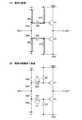
図2に本実施の形態のインバータの構成を示す。201は補正手段に相当し、202は
回路素子群である。FIG. 2 shows the configuration of the inverter of this embodiment. 201 corresponds to the correction means, and 202 is a group of circuit elements.
補正手段201は第1の容量素子203と、第2の容量素子204と、前記第1の容量
素子203への電位の供給を制御する3つのスイッチ205~207と、前記第2の容量
素子204への電位の供給を制御する3つのスイッチ208~210とを有している。The correction means 201 includes a
スイッチ205は、第1の容量素子203が有する第1の電極への、入力信号の電位の
供給を制御する。スイッチ206は、第1の容量素子203が有する第1の電極への、高
電位側の電源電位VHの供給を制御する。スイッチ207は、第1の容量素子203が有
する第2の電極への、電源電位VDDの供給を制御する。The
またスイッチ208は、第2の容量素子204が有する第1の電極への、入力信号の電
位の供給を制御する。スイッチ209は、第2の容量素子204が有する第1の電極への
、低電位側の電源電位VLの供給を制御する。スイッチ210は、第2の容量素子204
が有する第2の電極への、電源電位VSSの供給を制御する。Further, the
Controls the supply of the power potential VSS to the second electrode of the.
なお本実施の形態では、スイッチ207によって、第1の容量素子203が有する第2
の電極へ電源電位VDDが供給される形態を示しているが、本発明はこれに限定されない
。第1の容量素子203が有する第2の電極に供給される電位は電源電位VDD以外の電
位であっても良く、入力信号の電位に合わせて、供給する電位を適宜調節できるようにし
ても良い。また同様に、スイッチ210によって、第2の容量素子204が有する第2の
電極へ電源電位VSSが供給される形態を示しているが、本発明はこれに限定されない。
第2の容量素子204が有する第2の電極に供給される電位は電源電位VSS以外の電位
であっても良く、入力信号の電位に合わせて、供給する電位を適宜調節できるようにして
も良い。In this embodiment, the
Although the present invention shows a form in which the power supply potential VDD is supplied to the electrodes of the present invention, the present invention is not limited to this. The potential supplied to the second electrode of the first
The potential supplied to the second electrode of the second
回路素子群202は、1つのpチャネル型トランジスタ211と、1つのnチャネル型
トランジスタ212とを有している。pチャネル型トランジスタ211の第1の端子(こ
こではソース)には電源電位VDDが与えられており、nチャネル型トランジスタ212
の第1の端子(ここではソース)には電源電位VSSが与えられている。またpチャネル
型トランジスタ211の第2の端子(ここではドレイン)とnチャネル型トランジスタ2
12の第2の端子(ここではドレイン)は互いに接続されており、これらの2つのトラン
ジスタの第2の端子の電位が、出力信号OUTの電位として後段の回路に供給される。The
The first terminal (here, the source) of the power supply potential VSS is given. Further, the second terminal (drain in this case) of the p-
The second terminal (here, the drain) of the twelve is connected to each other, and the potential of the second terminal of these two transistors is supplied to the circuit of the subsequent stage as the potential of the output signal OUT.
また、第1の容量素子203の第2の電極はpチャネル型トランジスタ211のゲート
に接続されており、第2の容量素子204の第2の電極はnチャネル型トランジスタ21
2のゲートに接続されている。Further, the second electrode of the first
It is connected to the gate of 2.
なお、VDD>VSSであり、VH>VLであり、VDD>VH、VL>VSSとする。そ
して電源電位VHは、通常動作の際の入力信号の高電位側の電位に近く、できればそれ以
下となるように設定するのが望ましい。そうすることで、高電位側の電位が供給されたと
きに、pチャネル型トランジスタ211がオフしやすくなる。また電源電位VLは、通常
動作の際の入力信号の低電位側の電位に近く、できればそれ以上となるように設定するの
が望ましい。そうすることで、低電位側の電位が供給されたときに、nチャネル型トラン
ジスタ212がオフしやすくなる。本実施の形態では入力信号の高電位側の電位が電源電
位VHと等しく、入力信号の低電位側の電位が電源電位VLと等しいものと仮定する。また
VH-VL>VTHn、VL-VH<VTHpとなるようにする。It should be noted that VDD> VSS, VH >VL , VDD> VH , andVL > VSS. The power supply potential VH is preferably set to be close to the potential on the high potential side of the input signal during normal operation, and preferably lower than that. By doing so, the p-
また、本実施の形態では、回路素子群202が有するpチャネル型トランジスタ211
とnチャネル型トランジスタ212の閾値電圧が0であると仮定してその動作について説
明をするが、実際の回路では閾値が0であるとは限らない。その場合、例えばpチャネル
型トランジスタ211の閾値電圧をVTHpとすると、VHは、通常動作の際の入力信号の高
電位側の電位よりも|VTHp|分以上高くなるように設定するのが望ましい。また例えば
nチャネル型トランジスタ212の閾値電圧をVTHnとすると、VLは、通常動作の際の入
力信号の低電位側の電位よりも|VTHn|分以上低くなるように設定するのが望ましい。
そうすることで、ノーマリオンになるのを防ぎつつ、pチャネル型トランジスタ211や
nチャネル型トランジスタ212をオンさせるときに、|VGS|を最大限に大きくしてよ
り高いオン電流を得ることができる。Further, in the present embodiment, the p-
The operation will be described on the assumption that the threshold voltage of the n-
By doing so, it is possible to obtain a higher on-current by maximizing | VGS | when turning on the p-
次に図3を用いて、図2に示したインバータの動作について説明する。本発明のデジタ
ル回路の動作は、補正するべき電位差を記憶する動作と、デジタル回路の本来の機能を果
たす通常の動作とに区別される。Next, the operation of the inverter shown in FIG. 2 will be described with reference to FIG. The operation of the digital circuit of the present invention is divided into an operation of storing the potential difference to be corrected and a normal operation of performing the original function of the digital circuit.
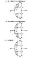
まず電位差を記憶する動作について、図3を用いて説明する。記憶するべき電位差は第
1の容量素子203と、第2の容量素子204とで異なる。第1の容量素子203では電
源電位VDDと高電位側電源電位VHとの電位差を記憶し、第2の容量素子204では電
源電位VSSと低電位側電源電位VLとの電位差を記憶する。First, the operation of storing the potential difference will be described with reference to FIG. The potential difference to be stored differs between the first
具体的には図3(A)に示すようにスイッチ205をオフ、スイッチ206、207を
オンにして、第1の容量素子203の第1の電極に電源電位VHを与え、第2の電極に電
源電位VDDを与える。そして第1の容量素子203には、電源電位VHと電源電位VD
Dとによって電荷が蓄積される。Specifically, as shown in FIG. 3A, the
Charges are accumulated by D and.
また、スイッチ208をオフ、スイッチ209、210をオンにして、第2の容量素子
204の第1の電極に電源電位VLを与え、第2の電極に電源電位VSSを与える。そし
て第2の容量素子204には、電源電位VLと電源電位VSSとによって電荷が蓄積され
る。Further, the
次に図3(B)に示すように、スイッチ205、206、207をオフにすることで、
蓄積された電荷が第1の容量素子203において保持され、電源電位VDDと電源電位V
Hとの間の電位差(Vc1と記する)が記憶される。また同様に、スイッチ208、209
、210をオフにすることで、蓄積された電荷が第2の容量素子204において保持され
、電源電位VSSと電源電位VLとの間の電位差(Vc2と記する)が記憶される。Next, as shown in FIG. 3B, by turning off the
The accumulated charge is held in the first
The potential difference withH (denoted as Vc1 ) is stored. Similarly, switches 208, 209
By turning off 210, the accumulated charge is retained in the second
次に、記憶された電位差による入力信号の電位の補正と、該補正された電位に基づいて
行なわれる通常動作について説明する。Next, the correction of the potential of the input signal by the stored potential difference and the normal operation performed based on the corrected potential will be described.
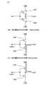
図4(A)を用いて、入力信号INの電位が、高電位側(本実施の形態ではVH)であ
る場合の動作について説明する。The operation when the potential of the input signal IN is on the high potential side (VH in this embodiment) will be described with reference to FIG. 4A.
通常の動作では、常にスイッチ206、207、209、210がオフし、スイッチ2
05、208がオンしている。入力信号の電位VHは、スイッチ205、208を介して
第1の容量素子203の第1の電極と、第2の容量素子204の第1の電極に与えられる
。In normal operation, switches 206, 207, 209 and 210 are always off and switch 2
05 and 208 are on. The potential VH of the input signal is applied to the first electrode of the first
第1の容量素子203と第2の容量素子204がそれぞれ有する2つの電極間の電位差
は、電荷保存の法則に従い、常に一定である。よって第1の容量素子203の第2の電極
の電位は、第1の電極に電位VHが与えられると、電位VHに電位差Vc1が加算された高
さに保たれる。ここで電位差Vc1=電源電位VDD-電源電位VHであるので、第1の容
量素子203の第2の電極の電位はVDDとなる。第2の電極の電位VDDはpチャネル
型トランジスタ211のゲートに与えられ、pチャネル型トランジスタ211はゲート電
圧が0となるのでオフになる。The potential difference between the two electrodes of the first
一方、第2の容量素子204の第2の電極の電位は、第1の電極に電位VHが与えられ
ると、電位VHに電位差Vc2が加算された高さに保たれる。ここで電位差Vc2=電源電
位VSS-電源電位VLであるので、第2の容量素子204の第2の電極の電位はVH+V
SS-VLとなる。よってnチャネル型トランジスタ212はゲート電圧がVH-VLとな
り、VH-VL>VTHnの場合はオンとなる。On the other hand, the potential of the second electrode of the
It becomes SS-VL . Therefore, the gate voltage of the n-
よって、入力信号INの電位がVHの場合、電源電位VSSが出力信号の電位として後
段の回路に与えられる。Therefore, when the potential of the input signal IN is VH , the power supply potential VSS is given to the subsequent circuit as the potential of the output signal.
次に図4(B)を用いて、入力信号INの電位が、低電位側(本実施の形態ではVL)
である場合の動作について説明する。Next, using FIG. 4B, the potential of the input signal IN is on the low potential side (VL in this embodiment).
The operation in the case of is described.
上述したように通常の動作ではスイッチ206、207、209、210がオフし、ス
イッチ205、208がオンしている。入力信号の電位VLは、スイッチ205、208
を介して第1の容量素子203の第1の電極と、第2の容量素子204の第1の電極に与
えられる。As described above, in normal operation, switches 206, 207, 209 and 210 are off and switches 205 and 208 are on. The potentialVL of the input signal is switches 205, 208.
It is given to the first electrode of the first
第1の容量素子203と第2の容量素子204がそれぞれ有する2つの電極間の電位差
は、電荷保存の法則に従い、常に一定である。よって第1の容量素子203の第2の電極
の電位は、第1の電極に電位VLが与えられると、電位VLに電位差Vc1が加算された高
さに保たれる。ここで電位差Vc1=電源電位VDD-電源電位VHであるので、第1の容
量素子203の第2の電極の電位はVL+VDD-VHとなる。よってpチャネル型トラン
ジスタ211はゲート電圧がVL-VHとなり、VL-VH<VTHpの場合はオンとなる。The potential difference between the two electrodes of the first
一方、第2の容量素子204の第2の電極の電位は、第1の電極に電位VLが与えられ
ると、電位VLに電位差Vc2が加算された高さに保たれる。ここで電位差Vc2=電源電
位VSS-電源電位VLであるので、第2の容量素子204の第2の電極の電位はVSS
となる。第2の電極の電位VSSはnチャネル型トランジスタ212のゲートに与えられ
、nチャネル型トランジスタ212はゲート電圧が0となるのでオフになる。On the other hand, the potential of the second electrode of the
Will be. The potential VSS of the second electrode is given to the gate of the n-
よって、入力信号INの電位がVLの場合、電源電位VDDが出力信号の電位として後
段の回路に与えられる。Therefore, when the potential of the input signal IN isVL , the power supply potential VDD is given to the subsequent circuit as the potential of the output signal.
本発明は上記構成によって、入力信号の電位にかかわらず、電位差VC1とVC2とを同時
に取得することができる。According to the above configuration, the present invention can simultaneously acquire the potential differencesVC1 andVC2 regardless of the potential of the input signal.
なお本実施の形態では、スイッチ207または210によって容量素子の第2の電極へ
の電源電位VSSまたはVDDの供給が制御されているが、本発明はこの構成に限定され
ない。スイッチ207によって電源電位VDDとは異なる電源電位VH’の、第1の容量
素子203の第2の電極への供給が制御されていても良い。また、スイッチ210によっ
て電源電位VSSとは異なる電源電位VL’の、第2の容量素子204の第2の電極への
供給が制御されていても良い。この場合、入力信号の高電位側の電位をVH''、低電位側
の電位をVL''とすると、VH''+VL’-VL-VSS>VTHnとし、またVL''+VH’-
VH-VDD<VTHpとする。さらに、VL''+VL’-VL-VSS≦VTHnであることが望
ましく、またVH''+VH’-VH-VDD≧VTHpであることが望ましい。In the present embodiment, the supply of the power supply potential VSS or VDD to the second electrode of the capacitive element is controlled by the
VH − VDD <VT Hp . Further, it is desirable that VL '' + VL' -VL -VSS ≤ VTHn , and VH '' + VH' -VH- VDD ≥ VTHp .
なお、スイッチ207または210によって第2の電極への電源電位VSSまたはVD
Dの供給が制御されている場合、電源電位VSSまたはVDDとは異なる電位VL’また
はVH’を供給する場合に比べて、電源電位を供給するための配線数を抑えることができ
る。The power potential VSS or VD to the second electrode by the
When the supply of D is controlled, the number of wires for supplying the power potential can be suppressed as compared with the case of supplying the potentialVL'or VH'different from the power potential VSS or VDD.
(実施の形態2)
本実施の形態では、本発明のデジタル回路の1つであるインバータの、実施の形態1と
は異なる構成について説明する。(Embodiment 2)
In the present embodiment, a configuration different from that of the first embodiment of the inverter, which is one of the digital circuits of the present invention, will be described.
図5に本実施の形態のインバータの構成を示す。301は補正手段に相当し、302は
回路素子群である。FIG. 5 shows the configuration of the inverter of this embodiment. 301 corresponds to the correction means, and 302 is a group of circuit elements.
補正手段301は第1の容量素子303と、第2の容量素子304と、前記第1の容量
素子303への電源電位VDDの供給を制御するスイッチ305と、前記第2の容量素子
304への電源電位VSSの供給を制御するスイッチ306とを有している。The correction means 301 is provided to the first
なお本実施の形態では、スイッチ305によって、第1の容量素子303が有する第2
の電極へ電源電位VDDが供給される形態を示しているが、本発明はこれに限定されない
。第1の容量素子303が有する第2の電極に供給される電位は電源電位VDD以外の電
位であっても良く、入力信号の電位に合わせて、供給する電位を適宜調節できるようにし
ても良い。また同様に、スイッチ306によって、第2の容量素子304が有する第2の
電極へ電源電位VSSが供給される形態を示しているが、本発明はこれに限定されない。
第2の容量素子304が有する第2の電極に供給される電位は電源電位VSS以外の電位
であっても良く、入力信号の電位に合わせて、供給する電位を適宜調節できるようにして
も良い。In this embodiment, the
The present invention shows a mode in which the power supply potential VDD is supplied to the electrodes of the above, but the present invention is not limited to this. The potential supplied to the second electrode of the first
The potential supplied to the second electrode of the second
回路素子群302は、1つのpチャネル型トランジスタ311と、1つのnチャネル型
トランジスタ312とを有している。pチャネル型トランジスタ311の第1の端子(こ
こではソース)には電源電位VDDが与えられており、nチャネル型トランジスタ312
の第1の端子(ここではソース)には電源電位VSSが与えられている。またpチャネル
型トランジスタ311の第2の端子(ここではドレイン)とnチャネル型トランジスタ3
12の第2の端子(ここではドレイン)は互いに接続されており、これら2つのトランジ
スタの第2の端子の電位が、出力信号OUTの電位として後段の回路に供給される。なお
、VDD>VSSである。また、VSSがnチャネル型トランジスタ312とスイッチ3
06に接続されている場合は、入力信号の高電位側の電位をVH、低電位側の電位をVLと
したときに、VH-VL>VTHn、VL-VH<VTHpとなるようにする。The
The first terminal (here, the source) of the power supply potential VSS is given. Further, the second terminal (drain in this case) of the p-
The second terminal (here, the drain) of the twelve is connected to each other, and the potential of the second terminal of these two transistors is supplied to the circuit of the subsequent stage as the potential of the output signal OUT. Note that VDD> VSS. In addition, VSS is an n-
When connected to 06, when the potential on the high potential side of the input signal is VH and the potential on the low potential side isVL , VH −VL > VTHn , VL −VH <V Make itTHp .
また、第1の容量素子303の第2の電極はpチャネル型トランジスタ311のゲート
に接続されており、第2の容量素子304の第2の電極はnチャネル型トランジスタ31
2のゲートに接続されている。Further, the second electrode of the first
It is connected to the gate of 2.
次に図6を用いて、図5に示したインバータの動作について説明する。図6に示したイ
ンバータの動作も、補正するべき電位差を記憶する動作と、デジタル回路の本来の機能を
果たす通常の動作とに区別される。ただし本実施の形態のインバータは、各容量素子への
電源電位の供給は、第1の容量素子と第2の容量素子とで同時に行なうのではなく、順に
行なう。Next, the operation of the inverter shown in FIG. 5 will be described with reference to FIG. The operation of the inverter shown in FIG. 6 is also divided into an operation of storing the potential difference to be corrected and a normal operation of performing the original function of the digital circuit. However, in the inverter of the present embodiment, the power supply potential is supplied to each capacity element in order, not simultaneously in the first capacity element and the second capacity element.
まず、第1の容量素子303において電位差を記憶する動作について、図6(A)を用
いて説明する。図6(A)に示すように、スイッチ305をオン、スイッチ306をオフ
にして、第1の容量素子303の第1の電極に入力信号INの高電位側の電位VHを与え
る。上記構成によって第1の容量素子303には、入力信号INの電位VHと電源電位V
DDとによって電荷が蓄積される。そして、スイッチ305をオフにし、第1の容量素子
303に蓄積された電荷が保持され、電源電位VDDと入力信号の高電位側の電位VHと
の間の電位差(Vc1と記する)が記憶される。First, the operation of storing the potential difference in the first
Charges are accumulated by the DD. Then, the
次に第2の容量素子304において電位差を記憶する動作について、図6(B)を用い
て説明する。図6(B)において、スイッチ305をオフ、スイッチ306をオンにして
、第2の容量素子304の第1の電極に入力信号INの低電位側の電位VLを与える。上
記構成によって第2の容量素子304には、入力信号INの電位VLと電源電位VSSと
によって電荷が蓄積される。そして、スイッチ306をオフにし、第2の容量素子304
に蓄積された電荷が保持され、電源電位VSSと入力信号の低電位側の電位VLとの間の
電位差(Vc2と記する)が記憶される。Next, the operation of storing the potential difference in the second
The electric charge accumulated in is retained, and the potential difference (denoted as Vc2 ) between the power supply potential VSS and the potentialVL on the low potential side of the input signal is stored.
なお、第1の容量素子303と第2の容量素子304への電荷の蓄積は、どちらを先に
行っても良い。Either of the
次に、記憶された電位差による入力信号の電位の補正と、該補正された電位に基づいて
行なわれる通常動作について説明する。図6(C)に示すように、通常動作の場合は、ス
イッチ305、306を常にオフにしておく。Next, the correction of the potential of the input signal by the stored potential difference and the normal operation performed based on the corrected potential will be described. As shown in FIG. 6C, switches 305 and 306 are always turned off during normal operation.
第1の容量素子303と第2の容量素子304がそれぞれ有する2つの電極間の電位差
は、電荷保存の法則に従い常に一定である。よって第1の容量素子303の第2の電極の
電位は、第1の電極に電位VHが与えられると、電位VHに電位差Vc1が加算された高さ
に保たれる。ここで電位差Vc1=電源電位VDD-入力信号の高電位側の電位VHである
ので、第1の容量素子303の第2の電極の電位はVDDとなる。第2の電極の電位VD
Dはpチャネル型トランジスタ311のゲートに与えられ、pチャネル型トランジスタ3
11はゲート電圧が0となるのでオフになる。The potential difference between the two electrodes of the first
D is given to the gate of the p-
11 is turned off because the gate voltage becomes 0.
一方、第2の容量素子304の第2の電極の電位は、第1の電極に電位VHが与えられ
ると、電位VHに電位差Vc2が加算された高さに保たれる。ここで電位差Vc2=電源電
位VSS-入力信号の低電位側の電位VLであるので、第2の容量素子304の第2の電
極の電位はVH+VSS-VLとなる。よってnチャネル型トランジスタ312はゲート電
圧がVH-VLとなり、VH-VL>VTHnであるのでオンとなる。On the other hand, the potential of the second electrode of the
よって、入力信号INの電位がVHの場合、電源電位VSSが出力信号の電位として後
段の回路に与えられる。Therefore, when the potential of the input signal IN is VH , the power supply potential VSS is given to the subsequent circuit as the potential of the output signal.
入力信号INの電位が低電位側の電位VLである場合、入力信号の電位VLは第1の容量
素子303の第1の電極と、第2の容量素子304の第1の電極に与えられる。When the potential of the input signal IN is the potentialVL on the low potential side, the potentialVL of the input signal is given to the first electrode of the first
第1の容量素子303と第2の容量素子304がそれぞれ有する2つの電極間の電位差
は、電荷保存の法則に従い常に一定である。よって第1の容量素子303の第2の電極の
電位は、第1の電極に電位VLが与えられると、電位VLに電位差Vc1が加算された高さ
に保たれる。ここで電位差Vc1=電源電位VDD-入力信号の高電位側の電位VHである
ので、第1の容量素子303の第2の電極の電位はVL+VDD-VHとなる。よってpチ
ャネル型トランジスタ311はゲート電圧がVL-VHとなり、VL-VH<VTHpであるの
でオンとなる。The potential difference between the two electrodes of the first
一方、第2の容量素子304の第2の電極の電位は、第1の電極に電位VLが与えられ
ると、電位VLに電位差Vc2が加算された高さに保たれる。ここで電位差Vc2=電源電
位VSS-入力信号の低電位側の電位VLであるので、第2の容量素子304の第2の電
極の電位はVSSとなる。第2の電極の電位VSSはnチャネル型トランジスタ312の
ゲートに与えられ、nチャネル型トランジスタ312はゲート電圧が0となるのでオフに
なる。On the other hand, the potential of the second electrode of the
よって、入力信号INの電位がVLの場合、電源電位VDDが出力信号の電位として後
段の回路に与えられる。Therefore, when the potential of the input signal IN isVL , the power supply potential VDD is given to the subsequent circuit as the potential of the output signal.
本発明は上記構成によって、入力信号の電位に関わらずデジタル回路を正常に動作させ
ることができる。また、図2に示したデジタル回路に比べて補正手段に用いるスイッチの
数を抑えることができ、より簡単な構成で本発明の効果を得ることができる。According to the above configuration, the present invention can normally operate a digital circuit regardless of the potential of an input signal. Further, as compared with the digital circuit shown in FIG. 2, the number of switches used for the correction means can be reduced, and the effect of the present invention can be obtained with a simpler configuration.
なお本実施の形態では、スイッチ305または306によって第2の電極への電源電位
VSSまたはVDDの供給が制御されているが、本発明はこの構成に限定されない。スイ
ッチ305によって電源電位VDDとは異なる電源電位VH’の、第1の容量素子303
の第2の電極への供給が制御されていても良い。また、スイッチ306によって電源電位
VSSとは異なる電源電位VL’の、第2の容量素子304の第2の電極への供給が制御
されていても良い。この場合、VH+VL’-VL-VSS>VTHnとし、またVL+VH’-
VH-VDD<VTHpとする。さらに、VL’-VSS≦VTHnであることが望ましく、また
VH’-VDD≧VTHpであることが望ましい。In the present embodiment, the supply of the power potential VSS or VDD to the second electrode is controlled by the
The supply to the second electrode may be controlled. Further, the
VH − VDD <VT Hp . Further, it is desirable that VL' -VSS ≤ VTHn , and VH'- VDD ≥ VTHp .
なお、スイッチ305または306によって第2の電極への電源電位VSSまたはVD
Dの供給が制御されている場合、電源電位VSSまたはVDDとは異なる電位VL’また
はVH’を供給する場合に比べて、電源電位を供給するための配線数を抑えることができ
る。The power potential VSS or VD to the second electrode by the
When the supply of D is controlled, the number of wires for supplying the power potential can be suppressed as compared with the case of supplying the potentialVL'or VH'different from the power potential VSS or VDD.
逆に、電源電位VSSまたはVDDとは異なる電位VL’またはVH’を供給する場合、
スイッチ305または306によって第2の電極への電源電位VSSまたはVDDの供給
が制御されている場合に比べて、各容量素子において記憶される電位差を、pチャネル型
トランジスタ311、nチャネル型トランジスタ312の閾値に合わせて適宜設定するこ
とができる。本実施の形態では、回路素子群302が有するpチャネル型トランジスタ3
11とnチャネル型トランジスタ312の閾値電圧が0であると仮定してその動作につい
て説明をしたが、実際の回路では閾値が0であるとは限らない。この場合、例えばpチャ
ネル型トランジスタ311の閾値電圧をVTHpとすると、VH’は、通常動作の際の入力信
号の高電位側の電位VHよりも|VTHp|分以上高くなるように設定するのが望ましい。ま
た例えばnチャネル型トランジスタ312の閾値電圧をVTHnとすると、VLは通常動作の
際の入力信号の低電位側の電位VLよりも|VTHn|分以上低くなるように設定するのが望
ましい。上記構成により、各トランジスタの閾値に合わせて入力信号を補正することがで
き、デジタル回路の動作をより確実なものにすることができる。Conversely, when supplying a potential VL' or VH'that is different from the power supply potential VSS or VDD,
Compared with the case where the supply of the power supply potential VSS or VDD to the second electrode is controlled by the
The operation has been described assuming that the threshold voltage of the 11 and the n-
(実施の形態3)
本実施の形態では、本発明のデジタル回路の1つであるNANDの構成について説明す
る。(Embodiment 3)
In this embodiment, the configuration of NAND, which is one of the digital circuits of the present invention, will be described.
図7に示す本実施の形態のNANDは、第1の補正手段401と、第2の補正手段40
2と、回路素子群403とを有している。The NAND of the present embodiment shown in FIG. 7 has a first correction means 401 and a second correction means 40.
2 and a
第1の補正手段401は第1の容量素子404と、第2の容量素子405と、前記第1
の容量素子404への電源電位VDDの供給を制御するスイッチ406と、前記第2の容
量素子405への電源電位VSSの供給を制御するスイッチ407とを有している。The first correction means 401 includes a first
It has a
また第2の補正手段402は第3の容量素子411と、第4の容量素子412と、前記
第3の容量素子411への電源電位VDDの供給を制御するスイッチ413と、前記第4
の容量素子412への電源電位VSSの供給を制御するスイッチ414とを有している。Further, the second correction means 402 includes a third capacitance element 411, a
It has a
回路素子群403は、2つのpチャネル型トランジスタ420、421と、2つのnチ
ャネル型トランジスタ422、423とを有している。pチャネル型トランジスタ420
の第1の端子(ここではソース)と、pチャネル型トランジスタ421の第1の端子(こ
こではソース)には電源電位VDDが与えられている。そして、pチャネル型トランジス
タ420の第2の端子(ここではドレイン)と、pチャネル型トランジスタ421の第2
の端子(ここではドレイン)は互いに接続されている。また、nチャネル型トランジスタ
422の第1の端子(ここではソース)には電源電位VSSが与えられている。また、n
チャネル型トランジスタ422の第2の端子(ここではドレイン)にはnチャネル型トラ
ンジスタ423の第1の端子(ここではソース)が接続されている。そしてnチャネル型
トランジスタ423の第2の端子(ここではドレイン)は、pチャネル型トランジスタ4
20、421の第2の端子に接続されている。なお、nチャネル型トランジスタ423の
第2の端子とpチャネル型トランジスタ420、421の第2の端子の電位が、出力信号
OUTの電位として後段の回路に与えられる。The
The power supply potential VDD is given to the first terminal (here, the source) of the p-
Terminals (here drains) are connected to each other. Further, a power supply potential VSS is given to the first terminal (here, the source) of the n-
The first terminal (here, source) of the n-
It is connected to the second terminal of 20, 421. The potentials of the second terminal of the n-
第1の容量素子404の第2の電極は、pチャネル型トランジスタ420のゲートに接
続されている。第2の容量素子405の第2の電極は、nチャネル型トランジスタ422
のゲートに接続されている。第3の容量素子411の第2の電極は、pチャネル型トラン
ジスタ421のゲートに接続されている。第4の容量素子412の第2の電極は、nチャ
ネル型トランジスタ423のゲートに接続されている。The second electrode of the first
It is connected to the gate of. The second electrode of the third capacitive element 411 is connected to the gate of the p-
第1の容量素子404の第1の電極と、第2の容量素子405の第1の電極に、入力信
号IN1の電位が入力される。また、第3の容量素子411の第1の電極と、第4の容量
素子412の第1の電極に、入力信号IN2の電位が入力される。The potential of the input signal IN1 is input to the first electrode of the
なお、VDD>VSSである。また入力信号の高電位側の電位をVH、低電位側の電位
をVLとし、pチャネル型トランジスタ420、421の閾値電圧をVTHpとし、nチャネ
ル型トランジスタ422、423の閾値電圧をVTHnとしたときに、VH-VL>VTHn、V
L-VH<VTHpとなるようにする。Note that VDD> VSS. Further, the potential on the high potential side of the input signal is VH , the potential on the low potential side isVL , the threshold voltage of the p-
L −VH <VTHp .
図7に示したNANDの動作も、補正するべき電位差を記憶する動作と、デジタル回路
の本来の機能を果たす通常の動作とに区別される。ただし本実施の形態のNANDは、各
容量素子への電源電位の供給は、第1の容量素子404と第2の容量素子405とで同時
に行なうのではなく順に行ない、また第3の容量素子411と第4の容量素子412とで
同時に行なうのではなく順に行なう。The operation of NAND shown in FIG. 7 is also divided into an operation of storing the potential difference to be corrected and a normal operation of performing the original function of the digital circuit. However, in the NAND of the present embodiment, the power supply potential is supplied to each capacitive element in order instead of being simultaneously supplied by the first
第1の容量素子404において電位差を記憶する際、スイッチ406をオン、スイッチ
407をオフにして、第1の容量素子404の第1の電極に入力信号IN1の高電位側の
電位VHを与える。そして電荷が十分蓄積された後、スイッチ406をオフにし、第1の
容量素子404に蓄積された電荷を保持する。また、第2の容量素子405において電位
差を記憶する際、スイッチ407をオン、スイッチ406をオフにして、第2の容量素子
405の第1の電極に入力信号IN1の低電位側の電位VLを与える。そして電荷が十分蓄
積された後、スイッチ407をオフにし、第2の容量素子405に蓄積された電荷を保持
する。When storing the potential difference in the
第3の容量素子411において電位差を記憶する際、スイッチ413をオン、スイッチ
414をオフにして、第3の容量素子411の第1の電極に入力信号IN2の高電位側の
電位VHを与える。そして電荷が十分蓄積された後、スイッチ413をオフにし、第3の
容量素子411に蓄積された電荷を保持する。また、第4の容量素子412において電位
差を記憶する際、スイッチ414をオン、スイッチ413をオフにして、第4の容量素子
412の第1の電極に入力信号IN2の低電位側の電位VLを与える。そして電荷が十分蓄
積された後、スイッチ414をオフにし、第4の容量素子412に蓄積された電荷を保持
する。When storing the potential difference in the third capacitance element 411, the
そして通常動作の際には、記憶された電位差によって入力信号の電位の補正が行なわれ
る。通常動作の際は、スイッチ406、407、413、414を常にオフにしておく。Then, during normal operation, the potential of the input signal is corrected by the stored potential difference. During normal operation, switches 406, 407, 413, 414 are always off.
本発明は上記構成によって、入力信号の電位に関わらずデジタル回路を正常に動作させ
ることができる。According to the above configuration, the present invention can normally operate a digital circuit regardless of the potential of an input signal.
なお本実施の形態では、スイッチ406、407、413、414によって第2の電極
への電源電位VSSまたはVDDの供給が制御されているが、本発明はこの構成に限定さ
れない。スイッチ406によって電源電位VDDとは異なる電源電位VH1’の、第1の容
量素子404の第2の電極への供給が制御されていても良い。また、スイッチ407によ
って電源電位VSSとは異なる電源電位VL1’の、第2の容量素子405の第2の電極へ
の供給が制御されていても良い。この場合、VH+VL1’-VL-VSS>VTHnとし、ま
たVL+VH1’-VH-VDD<VTHpとする。さらに、VL1’-VSS≦VTHnであること
が望ましく、またVH1’-VDD≧VTHpであることが望ましい。In the present embodiment, the supply of the power supply potential VSS or VDD to the second electrode is controlled by the
また、スイッチ413によって電源電位VDDとは異なる電源電位VH2’の、第3の容
量素子411の第2の電極への供給が制御されていても良い。また、スイッチ414によ
って電源電位VSSとは異なる電源電位VL2’の、第4の容量素子412の第2の電極へ
の供給が制御されていても良い。この場合、VH+VL2’-VL-VSS>VTHnとし、ま
たVL+VH2’-VH-VDD<VTHpとする。さらに、VL2’-VSS≦VTHnであること
が望ましく、またVH2’-VDD≧VTHpであることが望ましい。Further, the supply of the power supply potential VH2'different from the power supply potential VDD to the second electrode of the third capacitive element 411 may be controlled by the
なお、スイッチ406、407、413、414によって第2の電極への電源電位VS
SまたはVDDの供給が制御されている場合、電源電位VSSまたはVDDとは異なる電
位を供給する場合に比べて、電源電位を供給するための配線数を抑えることができる。The power potential VS to the second electrode by
When the supply of S or VDD is controlled, the number of wires for supplying the power potential can be suppressed as compared with the case of supplying a potential different from the power potential VSS or VDD.
逆に、電源電位VSSまたはVDDとは異なる電位を供給する場合、スイッチ406、
407、413、414によって第2の電極への電源電位VSSまたはVDDの供給が制
御されている場合に比べて、各容量素子において記憶される電位差を、各トランジスタ4
20~423の閾値に合わせて適宜設定することができる。例えばpチャネル型トランジ
スタ420、421の閾値電圧をVTHpとすると、VH1’またはVH2’は、通常動作の際
の入力信号の高電位側の電位VHよりも|VTHp|分以上高くなるように設定するのが望ま
しい。また例えばnチャネル型トランジスタ421、423の閾値電圧をVTHnとすると
、VL1’またはVL2’は通常動作の際の入力信号の低電位側の電位VLよりも|VTHn|分
以上低くなるように設定するのが望ましい。上記構成により、各トランジスタの閾値に合
わせて入力信号を補正することができ、デジタル回路の動作をより確実なものにすること
ができる。Conversely, if a potential different from the power potential VSS or VDD is supplied,
Compared with the case where the supply of the power supply potential VSS or VDD to the second electrode is controlled by 407, 413, 414, the potential difference stored in each capacitive element is stored in each transistor 4.
It can be appropriately set according to the threshold value of 20 to 423. For example, assuming that the threshold voltage of the p-
なお本実施の形態では、図5と同様に図1(C)に示す第2の構成を用いた場合につい
て示したが、図4と同様に図1(B)に示す第1の構成を用いることもできる。In this embodiment, the case where the second configuration shown in FIG. 1 (C) is used as in FIG. 5, but the first configuration shown in FIG. 1 (B) is used as in FIG. You can also do it.
また、本実施の形態ではNANDの場合を示したが、NORやトランスミッションゲー
トなど様々な論理回路にも同様に適用することができる。Further, although the case of NAND is shown in this embodiment, it can be similarly applied to various logic circuits such as NOR and transmission gate.
(実施の形態4)
本実施の形態では、本発明のデジタル回路の1つであるクロックドインバータの構成に
ついて説明する。(Embodiment 4)
In this embodiment, the configuration of a clocked inverter, which is one of the digital circuits of the present invention, will be described.
図8(A)に示す本実施の形態のクロックドインバータは、補正手段501と、回路素
子群502とを有している。The clocked inverter of the present embodiment shown in FIG. 8A has a correction means 501 and a
補正手段501は第1の容量素子503と、第2の容量素子504と、前記第1の容量
素子503への電源電位VDDの供給を制御するスイッチ505と、前記第2の容量素子
504への電源電位VSSの供給を制御するスイッチ506とを有している。The correction means 501 is provided to the
回路素子群502は、2つのpチャネル型トランジスタ520、521と、2つのnチ
ャネル型トランジスタ522、523とを有している。pチャネル型トランジスタ520
の第1の端子(ここではソース)には電源電位VDDが与えられている。そして、pチャ
ネル型トランジスタ520の第2の端子(ここではドレイン)と、pチャネル型トランジ
スタ521の第1の端子(ここではソース)は互いに接続されている。また、nチャネル
型トランジスタ523の第1の端子(ここではソース)には電源電位VSSが与えられて
いる。また、nチャネル型トランジスタ523の第2の端子(ここではドレイン)にはn
チャネル型トランジスタ522の第1の端子(ここではソース)が接続されている。そし
てnチャネル型トランジスタ522の第2の端子(ここではドレイン)は、pチャネル型
トランジスタ521の第2の端子(ここではドレイン)に接続されている。なお、nチャ
ネル型トランジスタ522の第2の端子とpチャネル型トランジスタ521の第2の端子
の電位が、出力信号OUTの電位として後段の回路に与えられる。The
The power potential VDD is given to the first terminal (source in this case) of the above. The second terminal (here, drain) of the p-
The first terminal (here, the source) of the
第1の容量素子503の第2の電極は、pチャネル型トランジスタ520のゲートに接
続されている。第2の容量素子504の第2の電極は、nチャネル型トランジスタ523
のゲートに接続されている。The second electrode of the first
It is connected to the gate of.
第1の容量素子503の第1の電極と、第2の容量素子504の第1の電極に、入力信
号INの電位が入力される。そして、pチャネル型トランジスタ521のゲートにクロッ
ク信号CKが、またnチャネル型トランジスタ522のゲートには、クロック信号の極性
が反転した信号に相当する反転クロック信号CKbが入力される。The potential of the input signal IN is input to the first electrode of the
なお、VDD>VSSである。また入力信号の高電位側の電位をVH、低電位側の電位
をVLとし、pチャネル型トランジスタ520の閾値電圧をVTHpとし、nチャネル型トラ
ンジスタ523の閾値電圧をVTHnとしたときに、VH-VL>VTHn、VL-VH<VTHpと
なるようにする。Note that VDD> VSS. When the potential on the high potential side of the input signal is VH , the potential on the low potential side isVL , the threshold voltage of the p-
図8(A)に示したクロックドインバータの動作も、実施の形態1~3と同様に、補正
するべき電位差を記憶する動作と、デジタル回路の本来の機能を果たす通常の動作とに区
別される。ただし本実施の形態のクロックドインバータは、各容量素子への電源電位の供
給は、第1の容量素子503と第2の容量素子504とで同時に行なうのではなく順に行
なう。The operation of the clocked inverter shown in FIG. 8A is also divided into an operation of storing the potential difference to be corrected and a normal operation of performing the original function of the digital circuit, as in the first to third embodiments. To. However, in the clocked inverter of the present embodiment, the power supply potential is supplied to each capacitance element in order instead of being simultaneously supplied by the
第1の容量素子503において電位差を記憶する際、スイッチ505をオン、スイッチ
506をオフにして、第1の容量素子503の第1の電極に入力信号INの高電位側の電
位VHを与える。そして電荷が十分蓄積された後、スイッチ505をオフにし、第1の容
量素子503に蓄積された電荷を保持する。また、第2の容量素子504において電位差
を記憶する際、スイッチ506をオン、スイッチ505をオフにして、第2の容量素子5
04の第1の電極に入力信号INの低電位側の電位VLを与える。そして電荷が十分蓄積
された後、スイッチ506をオフにし、第2の容量素子504に蓄積された電荷を保持す
る。When storing the potential difference in the
The potentialVL on the low potential side of the input signal IN is applied to the first electrode of 04. Then, after the electric charge is sufficiently accumulated, the
そして通常動作の際には、記憶された電位差によって入力信号の電位の補正が行なわれ
る。通常動作の際は、スイッチ505、506を常にオフにしておく。Then, during normal operation, the potential of the input signal is corrected by the stored potential difference. During normal operation, the
本発明は上記構成によって、入力信号の電位に関わらずデジタル回路を正常に動作させ
ることができる。According to the above configuration, the present invention can normally operate a digital circuit regardless of the potential of an input signal.
なお、pチャネル型トランジスタ521とpチャネル型トランジスタ520の接続は必
ずしも図8(A)に示した構成に限定されない。例えば、pチャネル型トランジスタ52
1によって、pチャネル型トランジスタ520のソースへの、電源電位VDDの供給が制
御されるように接続されていても良い。The connection between the p-
1 may be connected so as to control the supply of the power supply potential VDD to the source of the p-
同様に、nチャネル型トランジスタ522とnチャネル型トランジスタ523の接続は
必ずしも図8(A)に示した構成に限定されない。例えば、nチャネル型トランジスタ5
22によって、nチャネル型トランジスタ523のソースへの、電源電位VSSの供給が
制御されるように接続されていても良い。Similarly, the connection between the n-
22 may be connected so as to control the supply of the power potential VSS to the source of the n-
次に、図8(A)とは異なる構成のクロックドインバータについて説明する。図8(B
)に示す本実施の形態のクロックドインバータは、補正手段501と、回路素子群502
の接続構成が、図8(A)に示すクロックドインバータとは異なっている。Next, a clocked inverter having a configuration different from that of FIG. 8A will be described. FIG. 8 (B
The clocked inverter of the present embodiment shown in)) has a correction means 501 and a
The connection configuration of is different from that of the clocked inverter shown in FIG. 8 (A).
具体的には、第1の容量素子503の第1の電極にクロック信号CKが、また第2の容
量素子504の第1の電極にクロック信号の極性が反転した信号に相当する反転クロック
信号CKbが入力される。そして、pチャネル型トランジスタ541のゲートと、nチャ
ネル型トランジスタ542のゲートには、入力信号INの電位が入力される。Specifically, the clock signal CK corresponds to the first electrode of the
そして、図8(A)の場合と同様に、その動作は、補正するべき電位差を記憶する動作
と、デジタル回路の本来の機能を果たす通常の動作とに区別される。ただし本実施の形態
のクロックドインバータは、各容量素子への電源電位の供給は、順に行っても良いし、同
時に行っても良い。Then, as in the case of FIG. 8A, the operation is divided into an operation of storing the potential difference to be corrected and a normal operation of performing the original function of the digital circuit. However, in the clocked inverter of the present embodiment, the power supply potential may be supplied to each capacitive element in order or at the same time.
第1の容量素子503において電位差を記憶する際、スイッチ505をオン、スイッチ
506をオフにして、第1の容量素子503の第1の電極にクロック信号CKの高電位側
の電位VHを与える。そして電荷が十分蓄積された後、スイッチ505をオフにし、第1
の容量素子503に蓄積された電荷を保持する。また、第2の容量素子504において電
位差を記憶する際、スイッチ506をオン、スイッチ505をオフにして、第2の容量素
子504の第1の電極に反転クロック信号CKbの低電位側VLの電位を与える。そして
電荷が十分蓄積された後、スイッチ506をオフにし、第2の容量素子504に蓄積され
た電荷を保持する。When storing the potential difference in the
Holds the charge stored in the
そして通常動作の際には、記憶された電位差によって入力信号の電位の補正が行なわれ
る。通常動作の際は、スイッチ505、506を常にオフにしておく。Then, during normal operation, the potential of the input signal is corrected by the stored potential difference. During normal operation, the
本発明は上記構成によって、入力信号の電位に関わらずデジタル回路を正常に動作させ
ることができる。According to the above configuration, the present invention can normally operate a digital circuit regardless of the potential of an input signal.
なお本実施の形態では、スイッチ505、506によって第2の電極への電源電位VS
SまたはVDDの供給が制御されているが、本発明はこの構成に限定されない。スイッチ
505によって電源電位VDDとは異なる電源電位VH’の、第1の容量素子503の第
2の電極への供給が制御されていても良い。また、スイッチ506によって電源電位VS
Sとは異なる電源電位VL’の、第2の容量素子504の第2の電極への供給が制御され
ていても良い。この場合、VH+VL’-VL-VSS>VTHnとし、またVL+VH’-VH
-VDD<VTHpとする。さらに、VL’-VSS≦VTHnであることが望ましく、またVH
’-VDD≧VTHpであることが望ましい。In this embodiment, the power supply potential VS to the second electrode by the
The supply of S or VDD is controlled, but the invention is not limited to this configuration. The
The supply of the power supply potentialVL'different from S to the second electrode of the
-Achievements <VTHp . Furthermore, it is desirable that VL' -VSS ≤ VTHn , and VH
It is desirable that ′-VDD ≧ VTHp .
なお、スイッチ505、506によって第2の電極への電源電位VSSまたはVDDの
供給が制御されている場合、電源電位VSSまたはVDDとは異なる電位を供給する場合
に比べて、電源電位を供給するための配線数を抑えることができる。When the supply of the power supply potential VSS or VDD to the second electrode is controlled by the
逆に、電源電位VSSまたはVDDとは異なる電位を供給する場合、スイッチ505、
506によって第2の電極への電源電位VSSまたはVDDの供給が制御されている場合
に比べて、各容量素子において記憶される電位差を、各トランジスタ540、543の閾
値に合わせて適宜設定することができる。例えばpチャネル型トランジスタ540の閾値
電圧をVTHpとすると、VH’は通常動作の際の入力信号の高電位側の電位VHよりも|VT
Hp|分以上高くなるように設定するのが望ましい。また例えばnチャネル型トランジスタ
543の閾値電圧をVTHnとすると、VL’は通常動作の際の入力信号の低電位側の電位V
Lよりも|VTHn|分以上低くなるように設定するのが望ましい。上記構成により、各トラ
ンジスタの閾値に合わせて入力信号を補正することができ、デジタル回路の動作をより確
実なものにすることができる。On the contrary, when supplying a potential different from the power supply potential VSS or VDD, the
Compared with the case where the supply of the power supply potential VSS or VDD to the second electrode is controlled by 506, the potential difference stored in each capacitive element can be appropriately set according to the threshold value of each
It is desirable to set it to be higher thanHp | minutes. Further, for example, when the threshold voltage of the n-
It is desirable to set it so that it is lower thanL by | VTHn | minutes or more. With the above configuration, the input signal can be corrected according to the threshold value of each transistor, and the operation of the digital circuit can be made more reliable.
なお、図8(A)と図8(B)とを組み合わせても良い。 In addition, FIG. 8A and FIG. 8B may be combined.
本発明において、適用可能なトランジスタの種類に限定はなく、非晶質シリコンや多結
晶シリコンに代表される非単結晶半導体膜を用いた薄膜トランジスタ(TFT)、半導体
基板やSOI基板を用いて形成されるMOS型トランジスタ、接合型トランジスタ、バイ
ポーラトランジスタ、有機半導体やカーボンナノチューブを用いたトランジスタ、その他
のトランジスタを適用することができる。また、トランジスタが配置されている基板の種
類に限定はなく、単結晶基板、SOI基板、ガラス基板などに配置することが出来る。In the present invention, the type of transistor that can be applied is not limited, and is formed by using a thin film transistor (TFT) using a non-single crystal semiconductor film typified by amorphous silicon or polycrystalline silicon, a semiconductor substrate, or an SOI substrate. MOS type transistors, junction type transistors, bipolar transistors, transistors using organic semiconductors and carbon nanotubes, and other transistors can be applied. Further, the type of the substrate on which the transistor is arranged is not limited, and the transistor can be arranged on a single crystal substrate, an SOI substrate, a glass substrate, or the like.
本発明のデジタル回路において用いられるトランジスタは、単結晶シリコンを用いて形
成されたトランジスタであっても良いし、SOIを用いたトランジスタであっても良いし
、多結晶シリコン、セミアモルファスシリコン(微結晶シリコン)、アモルファスシリコ
ンを用いた薄膜トランジスタであっても良い。また、有機半導体を用いたトランジスタで
あっても良いし、カーボンナノチューブを用いたトランジスタであってもよい。The transistor used in the digital circuit of the present invention may be a transistor formed by using monocrystalline silicon, a transistor using SOI, a polycrystalline silicon, or a semi-amorphous silicon (microcrystal). Silicon), a thin film transistor using amorphous silicon may be used. Further, it may be a transistor using an organic semiconductor or a transistor using carbon nanotubes.
なお本実施の形態では、図5と同様に図1(C)に示す第2の構成を用いた場合につい
て示したが、図4と同様に図1(B)に示す第1の構成を用いることもできる。In this embodiment, the case where the second configuration shown in FIG. 1 (C) is used as in FIG. 5, but the first configuration shown in FIG. 1 (B) is used as in FIG. You can also do it.
(実施の形態5)
本実施の形態では、図2に示した本発明のインバータにおいて、第1の容量素子203
が有する第2の電極に供給される電位を、電源電位VDD以外の電位とし、また、第2の
容量素子204が有する第2の電極に供給される電位を、電源電位VSS以外の電位とす
る形態について説明する。(Embodiment 5)
In the present embodiment, in the inverter of the present invention shown in FIG. 2, the first
The potential supplied to the second electrode of the second electrode is a potential other than the power supply potential VDD, and the potential supplied to the second electrode of the second
図16(A)に、本実施の形態のインバータの構成を示す。図2において既に示したも
のには同じ符号を付す。図16(A)では、第1の容量素子203にpチャネル型トラン
ジスタ211の閾値電圧分の電荷が蓄積されるように、また第2の容量素子204にnチ
ャネル型トランジスタ212の閾値電圧分の電荷が蓄積されるように、各電源電圧の値を
最適化する。本実施の形態では、スイッチ206によって第1の容量素子203の第1の
電極に供給される電位をVDD、またスイッチ207によって第1の容量素子203の第
2の電極に供給される電位をVDD-|VTHp|とする。また、スイッチ209によって
第2の容量素子204の第1の電極に供給される電位をVSS、またスイッチ210によ
って第2の容量素子204の第2の電極に供給される電位をVSS+|VTHn|とする。FIG. 16A shows the configuration of the inverter of this embodiment. Those already shown in FIG. 2 are designated by the same reference numerals. In FIG. 16A, the charge for the threshold voltage of the p-
図16(B)~図16(D)を用いて、図16(A)に示したインバータの動作につい
て説明する。The operation of the inverter shown in FIG. 16 (A) will be described with reference to FIGS. 16 (B) to 16 (D).
まず、第1の容量素子203と、第2の容量素子204において、電荷の蓄積を行なう
。本実施の形態では、第1の容量素子203の第2電極の電位と、pチャネル型トランジ
スタ211のソースの電位を個別に制御でき、また第2の容量素子204の第2電極の電
位と、nチャネル型トランジスタ212のソースの電位を個別に制御できる。よって、第
1の容量素子203と第2の容量素子204における電荷の蓄積を並行して行なうことが
できる。First, electric charges are accumulated in the first
ます図16(B)に示すように、スイッチ206、207、209、210をオンに、
スイッチ205、208をオフすることで、第1の容量素子203にpチャネル型トラン
ジスタ211の閾値電圧を記憶し、第2の容量素子204にnチャネル型トランジスタ2
12の閾値電圧を記憶する。そして、スイッチ206、207、209、210をオフに
することで、蓄積された電荷が第1の容量素子203及び第2の容量素子204において
保持される。As shown in FIG. 16 (B), the
By turning off the
Twelve threshold voltages are stored. Then, by turning off the
次に、記憶された電位差による入力信号の電位の補正と、該補正された電位に基づいて
行なわれる通常動作について説明する。Next, the correction of the potential of the input signal by the stored potential difference and the normal operation performed based on the corrected potential will be described.
図16(C)を用いて、入力信号INの電位が、電源電位VDDと同じ場合について説
明する。通常の動作では、常にスイッチ206、207、209、210がオフし、スイ
ッチ205、208がオンしている。入力信号の電位は、スイッチ205、208を介し
て第1の容量素子203の第1の電極と、第2の容量素子204の第1の電極に与えられ
る。A case where the potential of the input signal IN is the same as the power supply potential VDD will be described with reference to FIG. 16 (C). In normal operation, switches 206, 207, 209 and 210 are always off and switches 205 and 208 are on. The potential of the input signal is applied to the first electrode of the first
第1の容量素子203には閾値電圧-|VTHp|が保持されているので、第1の容量素
子203の第2の電極の電位は、VDD-|VTHp|となる。よって、pチャネル型トラ
ンジスタ211は、そのゲート電圧VGSp=-|VTHp|となるため、オフする。Since the threshold voltage − | VTHp | is held in the first
一方、第2の容量素子204には閾値電圧|VTHn|が保持されているので、第2の容
量素子204の第2の電極の電位は、VDD+|VTHn|となる。よって、nチャネル型
トランジスタ212は、そのゲート電圧VGSn=VDD-VSS+|VTHn|>|VTHn|
となるので、オンする。On the other hand, since the threshold voltage | VTHn | is held in the second
So turn it on.
よって、入力信号INの電位がVDDの場合、電源電位VSSが出力信号の電位として
後段の回路に与えられる。Therefore, when the potential of the input signal IN is VDD, the power supply potential VSS is given to the subsequent circuit as the potential of the output signal.
図16(D)を用いて、入力信号INの電位が、電源電位VSSと同じ場合について説
明する。図16(C)の場合と同様に、通常の動作ではスイッチ206、207、209
、210がオフし、スイッチ205、208がオンしている。入力信号の電位は、スイッ
チ205、208を介して第1の容量素子203の第1の電極と、第2の容量素子204
の第1の電極に与えられる。A case where the potential of the input signal IN is the same as the power supply potential VSS will be described with reference to FIG. 16 (D). As in the case of FIG. 16C, switches 206, 207, 209 in normal operation.
, 210 are off and switches 205, 208 are on. The potential of the input signal is the first electrode of the first
Is given to the first electrode of.
第1の容量素子203には閾値電圧-|VTHp|が保持されているので、第1の容量素
子203の第2の電極の電位は、VSS-|VTHp|となる。よって、pチャネル型トラ
ンジスタ211は、そのゲート電圧VGSp=VSS-VDD-|VTHp|<-|VTHp|と
なるため、オンする。Since the threshold voltage − | VTHp | is held in the first
一方、第2の容量素子204には閾値電圧|VTHn|が保持されているので、第2の容
量素子204の第2の電極の電位は、VSS+|VTHn|となる。よって、nチャネル型
トランジスタ212は、そのゲート電圧VGSn=|VTHn|となるので、オフする。On the other hand, since the threshold voltage | VTHn | is held in the second
よって、入力信号INの電位がVSSの場合、電源電位VDDが出力信号の電位として
後段の回路に与えられる。Therefore, when the potential of the input signal IN is VSS, the power supply potential VDD is given to the subsequent circuit as the potential of the output signal.
本実施の形態では、電源電位がトランジスタのしきい値電圧の絶対値に対して十分大き
くない場合でもトランジスタの動作速度を向上させることができ、よって、デジタル回路
の消費電力を低減させることができる。In the present embodiment, the operating speed of the transistor can be improved even when the power supply potential is not sufficiently large with respect to the absolute value of the threshold voltage of the transistor, and thus the power consumption of the digital circuit can be reduced. ..
(実施の形態6)
本実施の形態では、図5に示した本発明のインバータにおいて、第1の容量素子303
が有する第2の電極に供給される電位を、電源電位VDD以外の電位とし、また、第2の
容量素子304が有する第2の電極に供給される電位を、電源電位VSS以外の電位とす
る形態について説明する。(Embodiment 6)
In the present embodiment, in the inverter of the present invention shown in FIG. 5, the first
The potential supplied to the second electrode of the second electrode is a potential other than the power supply potential VDD, and the potential supplied to the second electrode of the second
図17(A)に、本実施の形態のインバータの構成を示す。図5において既に示したも
のには同じ符号を付す。図17(A)では、第1の容量素子303にpチャネル型トラン
ジスタ311の閾値電圧分の電荷が蓄積されるように、また第2の容量素子304にnチ
ャネル型トランジスタ312の閾値電圧分の電荷が蓄積されるように、各電源電圧の値を
最適化する。本実施の形態では、スイッチ305によって第1の容量素子303の第2の
電極に供給される電位をVDD-|VTHp|とする。また、スイッチ306によって第2
の容量素子304の第2の電極に供給される電位をVSS+|VTHn|とする。FIG. 17A shows the configuration of the inverter of this embodiment. Those already shown in FIG. 5 are designated by the same reference numerals. In FIG. 17A, the electric charge corresponding to the threshold voltage of the p-
Let the potential supplied to the second electrode of the
図17(B)~図17(D)を用いて、図17(A)に示したインバータの動作につい
て説明する。The operation of the inverter shown in FIG. 17A will be described with reference to FIGS. 17B to 17D.
まず、第1の容量素子303と、第2の容量素子304において、電荷の蓄積を行なう
。First, electric charges are accumulated in the first
まず図17(B)に示すように、スイッチ305をオンに、スイッチ306をオフする
。そして入力信号としてVDDを入力することで、第1の容量素子303にpチャネル型
トランジスタ311の閾値電圧を記憶する。そしてスイッチ305をオフにすることで、
蓄積された電荷が第1の容量素子303において保持される。First, as shown in FIG. 17B, the
The accumulated charge is retained in the first
次に図17(C)に示すように、スイッチ306をオンに、スイッチ305をオフする
。そして入力信号としてVSSを入力することで、第2の容量素子304にnチャネル型
トランジスタ312の閾値電圧を記憶する。そしてスイッチ306をオフにすることで、
蓄積された電荷が第2の容量素子304において保持される。Next, as shown in FIG. 17C, the
The accumulated charge is retained in the second
次に、記憶された電位差による入力信号の電位の補正と、該補正された電位に基づいて
行なわれる通常動作について説明する。Next, the correction of the potential of the input signal by the stored potential difference and the normal operation performed based on the corrected potential will be described.
図17(D)を用いて、入力信号INの電位が、電源電位VDDと同じ場合について説
明する。通常の動作では、常にスイッチ305、306はオフしている。入力信号の電位
は、第1の容量素子303の第1の電極と、第2の容量素子304の第1の電極に与えら
れる。A case where the potential of the input signal IN is the same as the power supply potential VDD will be described with reference to FIG. 17 (D). In normal operation, switches 305 and 306 are always off. The potential of the input signal is given to the first electrode of the first
第1の容量素子303には閾値電圧-|VTHp|が保持されているので、第1の容量素
子303の第2の電極の電位は、VDD-|VTHp|となる。よって、pチャネル型トラ
ンジスタ311は、そのゲート電圧VGSp=-|VTHp|となるため、オフする。Since the threshold voltage − | VTHp | is held in the first
一方、第2の容量素子304には閾値電圧|VTHn|が保持されているので、第2の容
量素子304の第2の電極の電位は、VDD+|VTHn|となる。よって、nチャネル型
トランジスタ312は、そのゲート電圧VGSn=VDD-VSS+|VTHn|>|VTHn|
となるので、オンする。On the other hand, since the threshold voltage | VTHn | is held in the second
So turn it on.
よって、入力信号INの電位がVDDの場合、電源電位VSSが出力信号の電位として
後段の回路に与えられる。Therefore, when the potential of the input signal IN is VDD, the power supply potential VSS is given to the subsequent circuit as the potential of the output signal.
次に、入力信号INの電位が、電源電位VSSと同じ場合について説明する。図17(
C)の場合と同様に、通常の動作ではスイッチ305、306がオフしている。入力信号
の電位は、第1の容量素子303の第1の電極と、第2の容量素子304の第1の電極に
与えられる。Next, a case where the potential of the input signal IN is the same as the power supply potential VSS will be described. Figure 17 (
As in the case of C), the
第1の容量素子303には閾値電圧-|VTHp|が保持されているので、第1の容量素
子303の第2の電極の電位は、VSS-|VTHp|となる。よって、pチャネル型トラ
ンジスタ311は、そのゲート電圧VGSp=VSS-VDD-|VTHp|<-|VTHp|と
なるため、オンする。Since the threshold voltage − | VTHp | is held in the first
一方、第2の容量素子304には閾値電圧|VTHn|が保持されているので、第2の容
量素子304の第2の電極の電位は、VSS+|VTHn|となる。よって、nチャネル型
トランジスタ312は、そのゲート電圧VGSn=|VTHn|となるので、オフする。On the other hand, since the threshold voltage | VTHn | is held in the second
よって、入力信号INの電位がVSSの場合、電源電位VDDが出力信号の電位として
後段の回路に与えられる。Therefore, when the potential of the input signal IN is VSS, the power supply potential VDD is given to the subsequent circuit as the potential of the output signal.
本実施の形態では、電源電位がトランジスタのしきい値電圧の絶対値に対して十分大き
くない場合でもトランジスタの動作速度を向上させることができ、よって、デジタル回路
の消費電力を低減させることができる。In the present embodiment, the operating speed of the transistor can be improved even when the power supply potential is not sufficiently large with respect to the absolute value of the threshold voltage of the transistor, and thus the power consumption of the digital circuit can be reduced. ..
以下、本発明の実施例について説明する。 Hereinafter, examples of the present invention will be described.
本実施例では、半導体表示装置の信号線駆動回路に、本発明のクロックドインバータを
用いた場合の、クロックドインバータの構成とその駆動について説明する。In this embodiment, the configuration of the clocked inverter and its driving when the clocked inverter of the present invention is used for the signal line drive circuit of the semiconductor display device will be described.
図9(A)に本実施例で用いられるクロックドインバータの回路図を示す。図9(A)
に示すクロックドインバータは、図8(A)に示したクロックドインバータのスイッチに
、トランジスタを用いたものに相当する。FIG. 9A shows a circuit diagram of the clocked inverter used in this embodiment. FIG. 9 (A)
The clocked inverter shown in FIG. 8 corresponds to a switch of the clocked inverter shown in FIG. 8A using a transistor.
なお本実施の形態では、図5と同様に図1(C)に示す第2の構成を用いた場合につい
て示したが、図4と同様に図1(B)に示す第1の構成を用いることもできる。In this embodiment, the case where the second configuration shown in FIG. 1 (C) is used as in FIG. 5, but the first configuration shown in FIG. 1 (B) is used as in FIG. You can also do it.
図9(A)に示すクロックドインバータは、第1の容量素子601と、第2の容量素子
602と、pチャネル型トランジスタ603、607、608と、nチャネル型トランジ
スタ604、609、610を有している。The clocked inverter shown in FIG. 9A includes a first
第1の容量素子601の第1の電極と第2の容量素子602の第1の電極は互いに接続
されており、入力信号INの電位が与えられる。第1の容量素子601の第2の電極はp
チャネル型トランジスタ607のゲートに接続されている。また、第2の容量素子602
の第2の電極はnチャネル型トランジスタ610のゲートに接続されている。The first electrode of the first
It is connected to the gate of the
The second electrode is connected to the gate of the n-
pチャネル型トランジスタ603の第1の端子には電源電位VDDが与えられており、
第2の端子は第1の容量素子601の第2の電極に接続されている。nチャネル型トラン
ジスタ604の第1の端子には電源電位VSSが与えられており、第2の端子は第2の容
量素子602の第2の電極に接続されている。The power supply potential VDD is given to the first terminal of the p-
The second terminal is connected to the second electrode of the first
pチャネル型トランジスタ607の第1の端子(ここではソース)には電源電位VDD
が与えられている。そして、pチャネル型トランジスタ607の第2の端子(ここではド
レイン)と、pチャネル型トランジスタ608の第1の端子(ここではソース)は互いに
接続されている。また、nチャネル型トランジスタ610の第1の端子(ここではソース
)には電源電位VSSが与えられている。また、nチャネル型トランジスタ610の第2
の端子(ここではドレイン)にはnチャネル型トランジスタ609の第1の端子(ここで
はソース)が接続されている。そしてnチャネル型トランジスタ609の第2の端子(こ
こではドレイン)は、pチャネル型トランジスタ608の第2の端子(ここではドレイン
)に接続されている。なお、nチャネル型トランジスタ609の第2の端子とpチャネル
型トランジスタ608の第2の端子の電位が、出力信号OUTの電位として後段の回路に
与えられる。The power supply potential VDD is connected to the first terminal (here, the source) of the p-
Is given. The second terminal (here, the drain) of the p-
The first terminal (here, the source) of the n-
図9(B)に、第2の容量素子602に電荷を蓄積する期間と、第1の容量素子601
に電荷を蓄積する期間と、通常動作する期間の、入力信号INの電位と、pチャネル型ト
ランジスタ603のゲートの電位と、nチャネル型トランジスタ604のゲートの電位の
タイミングチャートを示す。FIG. 9B shows a period for accumulating electric charges in the second
The timing chart of the potential of the input signal IN, the potential of the gate of the p-
図9(B)に示すように、第2の容量素子602への電荷蓄積期間において、pチャネ
ル型トランジスタ603は、電源電位VDDに閾値電圧を加算した電位より高い電位がゲ
ートに与えられ、オフとなる。また、nチャネル型トランジスタ604は、電源電位VS
Sに閾値電圧を加算した電位より高い電位がゲートに与えられ、オンとなる。そして入力
信号INの電位は低電圧側の電位VLに保たれる。As shown in FIG. 9B, during the charge accumulation period in the second
A potential higher than the potential obtained by adding the threshold voltage to S is given to the gate, and the potential is turned on. The potential of the input signal IN is maintained at the potentialVL on the low voltage side.
そして、第2の容量素子602に十分電荷が蓄積されたら、nチャネル型トランジスタ
604のゲートに、電源電位VSSから閾値電圧分より低い電位が与えられてオフとなり
、第2の容量素子602に電荷が保持された状態になる。When sufficient charge is accumulated in the second
次に第1の容量素子601への電荷蓄積期間において、pチャネル型トランジスタ60
3は、電源電位VDDに閾値電圧を加算した電位より低い電位がゲートに与えられ、オン
となる。また、nチャネル型トランジスタ604は、電源電位VSSに閾値電圧を加算し
た電位より低い電位がゲートに与えられ、オフとなる。そして入力信号INの電位は高電
圧側の電位VHに保たれる。Next, during the charge accumulation period on the first
In No. 3, a potential lower than the potential obtained by adding the threshold voltage to the power supply potential VDD is given to the gate and the gate is turned on. Further, the n-
そして、第2の容量素子602に十分電荷が蓄積されたら、pチャネル型トランジスタ
604のゲートに、電源電位VSSに閾値電圧を加算した電位より高い電位が与えられて
オフとなり、第2の容量素子602に電荷が保持された状態になる。Then, when a sufficient charge is accumulated in the second
なお図9(B)では、第2の容量素子602への電荷の蓄積を、第1の容量素子601
への電荷の蓄積より先に行なっているが、逆であってもよい。すなわち、第1の容量素子
601への電荷の蓄積を行なった後、第2の容量素子602への電荷の蓄積を行なうよう
にしても良い。Note that in FIG. 9B, the accumulation of electric charge in the second
It is done before the charge is accumulated in, but it may be reversed. That is, the electric charge may be accumulated in the first
そして、通常動作期間においては、pチャネル型トランジスタ603は、電源電位VD
Dに閾値電圧を加算した電位より高い電位がゲートに与えられ、オフとなる。またnチャ
ネル型トランジスタ604は、電源電位VSSに閾値電圧を加算した電位より低い電位が
ゲートに与えられ、オフとなる。Then, during the normal operating period, the p-
A potential higher than the potential obtained by adding the threshold voltage to D is given to the gate, and the potential is turned off. Further, the n-
図10に、本実施例のクロックドインバータを用いた信号線駆動回路の構成を示す。本
実施例の信号線駆動回路は、シフトレジスタ1001と、ラッチA1002と、ラッチB
1003とを有する。ラッチA1002とラッチB1003は、複数段のラッチを有して
おり、本実施例のクロックドインバータは各ラッチに用いられている。FIG. 10 shows a configuration of a signal line drive circuit using the clocked inverter of this embodiment. The signal line drive circuit of this embodiment includes a shift register 1001, a latch A1002, and a latch B.
It has 1003 and. The latch A1002 and the latch B1003 have a plurality of stages of latches, and the clocked inverter of this embodiment is used for each latch.
具体的には図10に示すように、本実施例のラッチA1002が有する各段のラッチは
、本実施例のクロックドインバータ1004、通常のクロックドインバータ1005と、
2つのインバータ1006、1007とを有している。Specifically, as shown in FIG. 10, the latches of each stage included in the latch A1002 of this embodiment are the clocked
It has two
通常のクロックドインバータ1005と、2つのインバータ1006、1007には電
源と同じ振幅の信号が入力されるとする。従って、通常の回路を用いれば良い。しかし、
ビデオ信号、つまりクロックドインバータ1004の入力信号には振幅の小さな信号が入
力されるとする。従って、図8、図9に示したような、本発明の回路を用いる必要がある
。It is assumed that a signal having the same amplitude as the power supply is input to the normal clocked
It is assumed that a signal having a small amplitude is input to a video signal, that is, an input signal of the clocked
本実施例のクロックドインバータの場合、ビデオ信号が入力信号INに相当し、シフト
レジスタから供給されるタイミング信号と、その極性を反転させた信号とが、一方はpチ
ャネル型トランジスタ608のゲートに入力され、他方はnチャネル型トランジスタ60
9のゲートに入力される。電荷の蓄積を行なう期間は、ラッチAが動作していない期間に
設ければ良い。例えば、帰線期間や時間階調のときの点灯期間(ドライバが動いていない
期間)などに設ければ良い。In the case of the clocked inverter of this embodiment, the video signal corresponds to the input signal IN, and the timing signal supplied from the shift register and the signal whose polarity is inverted are one of the gates of the p-
It is input to the gate of 9. The period for accumulating the electric charge may be provided during the period during which the latch A is not operating. For example, it may be provided during the return line period or the lighting period during the time gradation (the period during which the driver is not moving).
あるいは、シフトレジスタ1001から出力される信号(サンプリングパルス)を用い
て、電荷の蓄積を行なうタイミングを制御しても良い。つまり、数列分前のサンプリング
パルスを用いて、電荷の蓄積を行っても良い。Alternatively, the signal (sampling pulse) output from the shift register 1001 may be used to control the timing of charge accumulation. That is, the charge may be accumulated by using the sampling pulse several sequences before.
図11に、クロックドインバータ1004、1005の上面図を示す。クロックドイン
バータ1004と1005は構成がほぼ同一であるため、クロックドインバータ1004
を例に挙げ、その構成について説明する。なお、図9(A)において既に示したものにつ
いては、同じ符号を付す。FIG. 11 shows a top view of the clocked
Is taken as an example, and its configuration will be described. The same reference numerals are given to those already shown in FIG. 9 (A).
1101は入力信号INが入力される配線であり、1102は出力信号OUTが出力さ
れる配線である。また1103はnチャネル型トランジスタ609のゲートに与えられる
電位が供給される配線であり、1104はpチャネル型トランジスタ608のゲートに与
えられる電位が供給される配線である。1105はnチャネル型トランジスタ604のゲ
ートに与えられる電位が供給される配線であり、1106はpチャネル型トランジスタ6
03のゲートに与えられる電位が供給される配線である。1101 is a wiring to which an input signal IN is input, and 1102 is a wiring to which an output signal OUT is output. Further, 1103 is a wiring to which the potential given to the gate of the n-
It is a wiring to which the potential given to the gate of 03 is supplied.
また、1120は電源電位VSSが供給されている配線であり、1121は電源電位V
DDが供給されている配線である。Further, 1120 is a wiring to which the power potential VSS is supplied, and 1121 is the power potential V.
This is the wiring to which the DD is supplied.
図11のA-A’における断面図を図12(A)に、B-B’における断面図を図12
(B)に示す。The cross-sectional view taken along the line AA'in FIG. 11 is shown in FIG. 12 (A), and the cross-sectional view taken along the line BB'is shown in FIG.
Shown in (B).
配線1200と配線1201は共に配線1106に接続されており、配線1200は配
線1220を介してpチャネル型トランジスタ603の第2の端子に接続されている。Both the
クロックドインバータ1004が有するpチャネル型トランジスタ608は、チャネル
形成領域1207と、第1の端子または第2の端子に相当する不純物領域1206、12
08と、ゲートに相当するゲート電極1202と、チャネル形成領域1207とゲート電
極1202間に設けられたゲート絶縁膜1224を有している。The p-
It has 08, a
クロックドインバータ1004が有するpチャネル型トランジスタ607は、チャネル
形成領域1209と、第1の端子または第2の端子に相当する不純物領域1208、12
10と、ゲートに相当するゲート電極1203と、チャネル形成領域1209とゲート電
極1203間に設けられたゲート絶縁膜1224を有している。The p-
It has a
クロックドインバータ1005が有するpチャネル型トランジスタ607は、チャネル
形成領域1211と、第1の端子または第2の端子に相当する不純物領域1210、12
12と、ゲートに相当するゲート電極1204と、チャネル形成領域1211とゲート電
極1204間に設けられたゲート絶縁膜1224を有している。The p-
It has a
クロックドインバータ1005が有するpチャネル型トランジスタ608は、チャネル
形成領域1213と、第1の端子または第2の端子に相当する不純物領域1212、12
14と、ゲートに相当するゲート電極1205と、チャネル形成領域1213とゲート電
極1205間に設けられたゲート絶縁膜1224を有している。The p-
It has a
なお、クロックドインバータ1004が有するpチャネル型トランジスタ608と、ク
ロックドインバータ1004が有するpチャネル型トランジスタ607は、不純物領域1
208を共有している。不純物領域1208は、クロックドインバータ1004が有する
pチャネル型トランジスタ608においてはソースに、クロックドインバータ1004が
有するpチャネル型トランジスタ607においてはドレインに相当する。The p-
It shares 208. The
また、クロックドインバータ1005が有するpチャネル型トランジスタ608と、ク
ロックドインバータ1005が有するpチャネル型トランジスタ607は、不純物領域1
212を共有している。不純物領域1212は、クロックドインバータ1005が有する
pチャネル型トランジスタ608においてはソースに、クロックドインバータ1005が
有するpチャネル型トランジスタ607においてはドレインに相当する。Further, the p-
It shares 212. The impurity region 1212 corresponds to the source in the p-
また、クロックドインバータ1004が有するpチャネル型トランジスタ607と、ク
ロックドインバータ1005が有するpチャネル型トランジスタ607は、不純物領域1
210を共有している。不純物領域1210は、両トランジスタにおいてソースに相当す
る。Further, the p-
It shares 210. The
不純物領域1206に配線1215が接続されている。また不純物領域1214に、配
線1217が接続されている。配線1215は、クロックドインバータ1004が有する
nチャネル型トランジスタ609のドレインに接続されている。
クロックドインバータ1004が有するpチャネル型トランジスタ607のゲート電極
1203は、配線1221を介してpチャネル型トランジスタ603の第2の端子に接続
されている。The
配線1223は、第1の容量素子601の半導体膜1226が有する不純物領域122
5に接続されている。半導体膜1226とゲート電極1203とがゲート絶縁膜1224
を間に挟んで重なることで形成される容量素子と、ゲート電極1203と配線1223と
が層間絶縁膜1230を間に挟んで重なることで形成される容量素子とが、共に第1の容
量素子601に相当する。The
It is connected to 5. The
The capacitive element formed by overlapping with the
このように容量素子をMOS容量として形成している。ただし、MOS容量は一方の電
極と他方の電極とで、電位の上下関係によっては容量値が非常に小さくなってしまう。従
って、容量素子を2つ並列に配置し、その極性や電極の向きなどを逆にすることにより、
電位の上下関係に関係なく容量素子として動作させている。In this way, the capacitive element is formed as a MOS capacitance. However, the MOS capacitance is between one electrode and the other electrode, and the capacitance value becomes very small depending on the vertical relationship of the potential. Therefore, by arranging two capacitive elements in parallel and reversing their polarities and electrode orientations,
It is operated as a capacitive element regardless of the vertical relationship of the potential.
なお容量素子は大きく形成している。なぜなら、入力信号INの電圧を印加しても容量
素子601とトランジスタ607のゲート容量とにより電圧分圧されるからである。例え
ば、容量素子601とトランジスタ607のゲート容量とが同じ大きさなら、入力信号I
Nの振幅のうち、半分しかトランジスタ607のゲートに加わらない。よって、容量素子
601は大きくする必要がある。基準としてはトランジスタ607のゲート容量の5倍の
大きさで容量素子601を形成するのが望ましい。なお、容量素子602と、トランジス
タ610の関係についても同様である。The capacitive element is large. This is because even if the voltage of the input signal IN is applied, the voltage is divided by the
Only half of the amplitude of N joins the gate of
なお本発明のデジタル回路の1つであるクロックドインバータは、図11に示す構成に
限定されない。例えば、シフトレジスタ1001が有するフリップフロップ回路を構成し
ているクロックドインバータに用いられていても良い。
この場合も、入力信号に振幅が小さい信号が入力される部分に本発明を適用すれば良い。
従って、シフトレジスタではクロック信号やその反転信号の振幅が小さいため、図8(A
)のクロックドインバータを用いれば良い。この場合、入力されるビデオ信号の帰線期間
においてシフトレジスタは動作していないので、該期間において電荷の蓄積を行なえば良
い。The clocked inverter, which is one of the digital circuits of the present invention, is not limited to the configuration shown in FIG. For example, it may be used in a clocked inverter constituting the flip-flop circuit included in the shift register 1001.
In this case as well, the present invention may be applied to a portion where a signal having a small amplitude is input to the input signal.
Therefore, since the amplitude of the clock signal and its inverting signal is small in the shift register, FIG. 8 (A)
) Clocked inverter may be used. In this case, since the shift register is not operating during the blanking interval of the input video signal, the charge may be accumulated during that period.
なお本発明のデジタル回路の1つであるクロックドインバータは、図11に示す構成に
限定されない。The clocked inverter, which is one of the digital circuits of the present invention, is not limited to the configuration shown in FIG.
本発明のデジタル回路を駆動回路に用いたあらゆる半導体装置は、本発明の範疇に含ま
れる。図15に本発明の半導体装置の1つである半導体表示装置の外観図を示す。図15
に示す半導体表示装置は、複数の画素が設けられた画素部1503と、画素を選択する走
査線駆動回路1501と、前記選択された画素にビデオ信号を供給する信号線駆動回路1
502とを有する。そして画素部1503、信号線駆動回路1502または走査線駆動回
路1501の駆動に用いられる各種信号及び電源電位は、FPC1504を介して供給さ
れる。Any semiconductor device using the digital circuit of the present invention as a drive circuit is included in the category of the present invention. FIG. 15 shows an external view of a semiconductor display device, which is one of the semiconductor devices of the present invention. FIG. 15
The semiconductor display device shown in the above is a
It has 502 and. The various signals and power supply potentials used to drive the
本発明の半導体表示装置には、液晶表示装置、有機発光素子に代表される発光素子を各
画素に備えた発光装置、DMD(Digital Micromirror Device)、PDP(Plasma Displ
ay Panel)、FED(Field Emission
Display)等や、半導体膜を用いた回路素子を駆動回路に有しているその他の表示装置が
含まれる。The semiconductor display device of the present invention includes a liquid crystal display device, a light emitting device having a light emitting element typified by an organic light emitting element in each pixel, a DMD (Digital Micromirror Device), and a PDP (Plasma Displ).
ay Panel), FED (Field Emission)
Display) and the like, and other display devices having a circuit element using a semiconductor film in the drive circuit are included.
また本発明の範疇に含まれる半導体装置には、半導体表示装置の他に、加算器、ALU
(Arithmetic Logic Unit)、カウンタ、乗算器、シフタ等を含む演算回路と、フリップ
フロップ、マルチポートRAM、FIFO(First In First Out)回路等を含む記憶回路
と、PLA(Programmable Logic Array)等を含む制御回路とを、いずれか単数または複
数有する半導体集積回路がある。Further, the semiconductor device included in the category of the present invention includes an adder and an ALU in addition to the semiconductor display device.
(Arithmetic Logic Unit), arithmetic circuit including counter, multiplier, shifter, etc., storage circuit including flip-flop, multi-port RAM, FIFA (First In First Out) circuit, etc., PLA (Programmable Logic Array), etc. There is a semiconductor integrated circuit having one or more control circuits.
本発明の半導体装置を用いた電子機器として、ビデオカメラ、デジタルカメラ、ゴーグ
ル型ディスプレイ(ヘッドマウントディスプレイ)、ナビゲーションシステム、音響再生
装置(カーオーディオ、オーディオコンポ等)、ノート型パーソナルコンピュータ、ゲー
ム機器、携帯情報端末(モバイルコンピュータ、携帯電話、携帯型ゲーム機または電子書
籍等)、記録媒体を備えた画像再生装置(具体的にはDigital Versatile Disc(DVD)
等の記録媒体を再生し、その画像を表示しうるディスプレイを備えた装置)などが挙げら
れる。それら電子機器の具体例を図18に示す。As electronic devices using the semiconductor device of the present invention, video cameras, digital cameras, goggle type displays (head mount displays), navigation systems, sound reproduction devices (car audio, audio components, etc.), notebook personal computers, game devices, etc. An image playback device equipped with a mobile information terminal (mobile computer, mobile phone, portable game machine, electronic book, etc.) and a recording medium (specifically, Digital Versatile Disc (DVD)).
A device equipped with a display capable of reproducing a recording medium such as the above and displaying the image) and the like. Specific examples of these electronic devices are shown in FIG.
図18(A)は表示装置であり、筐体2001、表示部2002、スピーカー部200
3等を含む。本発明の半導体装置は、表示部2002に用いることができる。表示装置に
は、パソコン用、TV放送受信用、広告表示用などの全ての情報表示用表示装置が含まれ
る。本発明の半導体装置は、表示部2002及びその他の信号処理回路に用いることがで
きる。なお表示装置に発光装置を用いる場合、発光素子が有する電極において外光が反射
することで、鏡面のように像を写してしまうのを防ぐために、偏光板を設けておいても良
い。FIG. 18A is a display device, which includes a
Including 3 mag. The semiconductor device of the present invention can be used for the
図18(B)はデジタルスチルカメラであり、本体2101、表示部2102、受像部
2103、操作キー2104、外部接続ポート2105、シャッター2106等を含む。
本発明の半導体装置を表示部2102またはその他の信号処理回路に用いることで、本発
明のデジタルスチルカメラが完成する。FIG. 18B is a digital still camera, which includes a
By using the semiconductor device of the present invention for the
図18(C)はノート型パーソナルコンピュータであり、本体2201、筐体2202
、表示部2203、キーボード2204、外部接続ポート2205、ポインティングマウ
ス2206等を含む。本発明の半導体装置を表示部2203またはその他の信号処理回路
に用いることで、本発明のノート型パーソナルコンピュータが完成する。FIG. 18C shows a notebook personal computer, which has a
,
図18(D)はモバイルコンピュータであり、本体2301、表示部2302、スイッ
チ2303、操作キー2304、赤外線ポート2305等を含む。本発明の半導体装置を
表示部2302またはその他の信号処理回路に用いることで、本発明のモバイルコンピュ
ータが完成する。FIG. 18D is a mobile computer, which includes a
図18(E)は記録媒体を備えた携帯型の画像再生装置(具体的にはDVD再生装置)
であり、本体2401、筐体2402、表示部A2403、表示部B2404、記録媒体
(DVD等)読み込み部2405、操作キー2406、スピーカー部2407等を含む。
表示部A2403は主として画像情報を表示し、表示部B2404は主として文字情報を
表示する。なお、記録媒体を備えた画像再生装置には家庭用ゲーム機器なども含まれる。
本発明の半導体装置を表示部A2403、B2404またはその他の信号処理回路に用い
ることで、本発明の画像再生装置が完成する。FIG. 18E shows a portable image playback device (specifically, a DVD playback device) provided with a recording medium.
It includes a
The display unit A2403 mainly displays image information, and the display unit B2404 mainly displays character information. The image reproduction device provided with the recording medium also includes a home-use game device and the like.
By using the semiconductor device of the present invention for the display units A2403, B2404 or other signal processing circuits, the image reproduction device of the present invention is completed.
図18(F)はゴーグル型ディスプレイ(ヘッドマウントディスプレイ)であり、本体
2501、表示部2502、アーム部2503を含む。本発明の半導体装置を表示部25
02またはその他の信号処理回路に用いることで、本発明のゴーグル型ディスプレイが完
成する。FIG. 18F is a goggle-type display (head-mounted display), which includes a
By using it in 02 or other signal processing circuits, the goggle type display of the present invention is completed.
図18(G)はビデオカメラであり、本体2601、表示部2602、筐体2603、
外部接続ポート2604、リモコン受信部2605、受像部2606、バッテリー260
7、音声入力部2608、操作キー2609等を含む。本発明の半導体装置を表示部26
02またはその他の信号処理回路に用いることで、本発明のビデオカメラが完成する。FIG. 18 (G) is a video camera, which includes a main body 2601, a
7. Includes
By using it in 02 or other signal processing circuits, the video camera of the present invention is completed.
ここで図18(H)は携帯電話であり、本体2701、筐体2702、表示部2703
、音声入力部2704、音声出力部2705、操作キー2706、外部接続ポート270
7、アンテナ2708等を含む。なお、表示部2703は黒色の背景に白色の文字を表示
することで携帯電話の消費電流を抑えることができる。本発明の半導体装置を表示部27
03またはその他の信号処理回路に用いることで、本発明の携帯電話が完成する。Here, FIG. 18 (H) is a mobile phone, which is a
,
7. Includes antenna 2708 and the like. The
By using it in 03 or other signal processing circuits, the mobile phone of the present invention is completed.
以上の様に、本発明の適用範囲は極めて広く、あらゆる分野の電子機器に用いることが
可能である。また、本実施例の電子機器は実施例1~9に示したいずれの構成を用いても
良い。As described above, the scope of application of the present invention is extremely wide, and it can be used for electronic devices in all fields. In addition, any of the configurations shown in Examples 1 to 9 may be used for the electronic device of this embodiment.
Claims (1)
Translated fromJapanese前記容量素子の第1の電極は、入力端子に電気的に接続され、
前記第1のトランジスタのソース又はドレインの一方は、前記配線に電気的に接続され、
前記第1のトランジスタのソース又はドレインの他方は、前記容量素子の第2の電極に電気的に接続され、
前記第2のトランジスタのゲートは、前記容量素子の第2の電極に電気的に接続され、
前記第2のトランジスタのソース又はドレインの一方は、前記配線に電気的に接続され、
前記第2のトランジスタのソース又はドレインの他方は、出力端子に電気的に接続されていることを特徴とする半導体装置。It has a capacitive element, first and second transistors, and wiring.
The first electrode of the capacitive element is electrically connected to the input terminal and
One of the source or drain of the first transistor is electrically connected to the wiring.
The other of the source or drain of the first transistor is electrically connected to the second electrode of the capacitive element.
The gate of the second transistor is electrically connected to the second electrode of the capacitive element.
One of the source or drain of the second transistor is electrically connected to the wiring.
A semiconductor device characterized in that the other of the source or drain of the second transistor is electrically connected to an output terminal.
Applications Claiming Priority (3)
| Application Number | Priority Date | Filing Date | Title |
|---|---|---|---|
| JP2003033051 | 2003-02-12 | ||
| JP2003033051 | 2003-02-12 | ||
| JP2020173171AJP2021013191A (en) | 2003-02-12 | 2020-10-14 | Liquid crystal display device |
Related Parent Applications (1)
| Application Number | Title | Priority Date | Filing Date |
|---|---|---|---|
| JP2020173171ADivisionJP2021013191A (en) | 2003-02-12 | 2020-10-14 | Liquid crystal display device |
Publications (1)
| Publication Number | Publication Date |
|---|---|
| JP2022037046Atrue JP2022037046A (en) | 2022-03-08 |
Family
ID=32677571
Family Applications (11)
| Application Number | Title | Priority Date | Filing Date |
|---|---|---|---|
| JP2009296866AExpired - Fee RelatedJP5008717B2 (en) | 2003-02-12 | 2009-12-28 | Semiconductor device |
| JP2012099513AExpired - Fee RelatedJP5352704B2 (en) | 2003-02-12 | 2012-04-25 | Semiconductor device |
| JP2013130207AWithdrawnJP2013225908A (en) | 2003-02-12 | 2013-06-21 | Semiconductor device |
| JP2014193179AExpired - LifetimeJP5948386B2 (en) | 2003-02-12 | 2014-09-23 | Semiconductor device, display device, module, and electronic device |
| JP2015220503AExpired - Fee RelatedJP6129278B2 (en) | 2003-02-12 | 2015-11-10 | Semiconductor device, display device, module, and electronic device |
| JP2016114499AWithdrawnJP2016178692A (en) | 2003-02-12 | 2016-06-08 | Semiconductor device, display device, module and electronic apparatus |
| JP2018009070AExpired - Fee RelatedJP6543360B2 (en) | 2003-02-12 | 2018-01-23 | Head mounted display |
| JP2018035021AWithdrawnJP2018093531A (en) | 2003-02-12 | 2018-02-28 | Liquid crystal display device |
| JP2019160619AWithdrawnJP2019208285A (en) | 2003-02-12 | 2019-09-03 | Semiconductor device |
| JP2020173171AWithdrawnJP2021013191A (en) | 2003-02-12 | 2020-10-14 | Liquid crystal display device |
| JP2021197272AWithdrawnJP2022037046A (en) | 2003-02-12 | 2021-12-03 | Semiconductor device |
Family Applications Before (10)
| Application Number | Title | Priority Date | Filing Date |
|---|---|---|---|
| JP2009296866AExpired - Fee RelatedJP5008717B2 (en) | 2003-02-12 | 2009-12-28 | Semiconductor device |
| JP2012099513AExpired - Fee RelatedJP5352704B2 (en) | 2003-02-12 | 2012-04-25 | Semiconductor device |
| JP2013130207AWithdrawnJP2013225908A (en) | 2003-02-12 | 2013-06-21 | Semiconductor device |
| JP2014193179AExpired - LifetimeJP5948386B2 (en) | 2003-02-12 | 2014-09-23 | Semiconductor device, display device, module, and electronic device |
| JP2015220503AExpired - Fee RelatedJP6129278B2 (en) | 2003-02-12 | 2015-11-10 | Semiconductor device, display device, module, and electronic device |
| JP2016114499AWithdrawnJP2016178692A (en) | 2003-02-12 | 2016-06-08 | Semiconductor device, display device, module and electronic apparatus |
| JP2018009070AExpired - Fee RelatedJP6543360B2 (en) | 2003-02-12 | 2018-01-23 | Head mounted display |
| JP2018035021AWithdrawnJP2018093531A (en) | 2003-02-12 | 2018-02-28 | Liquid crystal display device |
| JP2019160619AWithdrawnJP2019208285A (en) | 2003-02-12 | 2019-09-03 | Semiconductor device |
| JP2020173171AWithdrawnJP2021013191A (en) | 2003-02-12 | 2020-10-14 | Liquid crystal display device |
Country Status (5)
| Country | Link |
|---|---|
| US (3) | US7528643B2 (en) |
| EP (1) | EP1447911B1 (en) |
| JP (11) | JP5008717B2 (en) |
| KR (1) | KR101055692B1 (en) |
| CN (3) | CN103107801B (en) |
Families Citing this family (26)
| Publication number | Priority date | Publication date | Assignee | Title |
|---|---|---|---|---|
| US7327168B2 (en)* | 2002-11-20 | 2008-02-05 | Semiconductor Energy Laboratory Co., Ltd. | Semiconductor device and driving method thereof |
| KR101114892B1 (en)* | 2002-12-25 | 2012-03-07 | 가부시키가이샤 한도오따이 에네루기 켄큐쇼 | Digital circuit having correction circuit and electronic instrument having same |
| US7528643B2 (en)* | 2003-02-12 | 2009-05-05 | Semiconductor Energy Laboratory Co., Ltd. | Semiconductor device, electronic device having the same, and driving method of the same |
| US7332936B2 (en)* | 2004-12-03 | 2008-02-19 | Semiconductor Energy Laboratory Co., Ltd. | Semiconductor circuit, display device, electronic apparatus |
| EP1717783B1 (en)* | 2005-04-28 | 2015-06-03 | Semiconductor Energy Laboratory Co., Ltd. | Data latch circuit, driving method of the data latch circuit, and display device |
| KR100621827B1 (en)* | 2005-08-08 | 2006-09-11 | 한국과학기술원 | Nonvolatile Mechanical Memory |
| JP5566568B2 (en)* | 2007-03-27 | 2014-08-06 | ピーエスフォー ルクスコ エスエイアールエル | Power supply voltage generation circuit |
| KR101329791B1 (en)* | 2007-07-16 | 2013-11-15 | 삼성디스플레이 주식회사 | Liquid crystal display |
| JP5093895B2 (en)* | 2008-03-12 | 2012-12-12 | 株式会社ジャパンディスプレイセントラル | Level shifter circuit |
| US7804328B2 (en)* | 2008-06-23 | 2010-09-28 | Texas Instruments Incorporated | Source/emitter follower buffer driving a switching load and having improved linearity |
| JP5394318B2 (en)* | 2010-05-20 | 2014-01-22 | 株式会社日本自動車部品総合研究所 | Differential communication device |
| JP5982147B2 (en) | 2011-04-01 | 2016-08-31 | 株式会社半導体エネルギー研究所 | Light emitting device |
| US8922464B2 (en) | 2011-05-11 | 2014-12-30 | Semiconductor Energy Laboratory Co., Ltd. | Active matrix display device and driving method thereof |
| KR101983976B1 (en) | 2011-05-13 | 2019-05-30 | 가부시키가이샤 한도오따이 에네루기 켄큐쇼 | Semiconductor device |
| KR102081792B1 (en) | 2011-05-19 | 2020-02-26 | 가부시키가이샤 한도오따이 에네루기 켄큐쇼 | Arithmetic circuit and method of driving the same |
| JP5947099B2 (en) | 2011-05-20 | 2016-07-06 | 株式会社半導体エネルギー研究所 | Semiconductor device |
| CN102347757B (en)* | 2011-05-24 | 2013-01-23 | 北京空间机电研究所 | Low-level adjustable high-voltage pulse converter |
| US8710505B2 (en) | 2011-08-05 | 2014-04-29 | Semiconductor Energy Laboratory Co., Ltd. | Semiconductor device |
| US8736315B2 (en)* | 2011-09-30 | 2014-05-27 | Semiconductor Energy Laboratory Co., Ltd. | Semiconductor device |
| US10043794B2 (en) | 2012-03-22 | 2018-08-07 | Semiconductor Energy Laboratory Co., Ltd. | Semiconductor device and electronic device |
| KR101931335B1 (en)* | 2012-03-23 | 2018-12-20 | 엘지디스플레이 주식회사 | Level shifter for liquid crystal display |
| US9245593B2 (en)* | 2013-10-16 | 2016-01-26 | Semiconductor Energy Laboratory Co., Ltd. | Method for driving arithmetic processing unit |
| TWI621127B (en)* | 2013-10-18 | 2018-04-11 | 半導體能源研究所股份有限公司 | Arithmetic processing unit and driving method thereof |
| AU2015397728B2 (en)* | 2015-06-01 | 2018-08-30 | Guangdong Oppo Mobile Telecommunications Corp., Ltd. | Charging circuit and mobile terminal |
| US12431884B2 (en)* | 2023-01-24 | 2025-09-30 | Blue Cheetah Analog Design, Inc. | Data communication link with capacitor-based pumped output |
| US20250185300A1 (en)* | 2023-12-05 | 2025-06-05 | Qualcomm Incorporated | Electronic devices employing thin-gate insulator transistors coupled to varactors to reduce gate-to-source/drain voltage to avoid voltage breakdown, and related fabrication methods |
Citations (1)
| Publication number | Priority date | Publication date | Assignee | Title |
|---|---|---|---|---|
| JP2001177388A (en)* | 1999-12-16 | 2001-06-29 | Hitachi Ltd | Drive circuit |
Family Cites Families (71)
| Publication number | Priority date | Publication date | Assignee | Title |
|---|---|---|---|---|
| US257117A (en)* | 1882-04-25 | Writing-tablet | ||
| JPS5543299B2 (en) | 1972-06-01 | 1980-11-05 | ||
| JPS596628A (en)* | 1982-07-05 | 1984-01-13 | Oki Electric Ind Co Ltd | Tri-state logical circuit |
| JPS6051322A (en)* | 1983-08-31 | 1985-03-22 | Toshiba Corp | CMOS voltage conversion circuit |
| JPS6065613A (en)* | 1983-09-21 | 1985-04-15 | Hitachi Ltd | Chiyotsupa type comparator |
| JPS60105320A (en) | 1983-11-14 | 1985-06-10 | Nippon Telegr & Teleph Corp <Ntt> | Level converting circuit |
| US4758801A (en)* | 1985-07-11 | 1988-07-19 | Siemens Aktiengesellschaft | Dynamic control system with switchable filter-function groups |
| US4649300A (en) | 1985-08-12 | 1987-03-10 | Intel Corporation | Bootstrap buffer |
| JPH04357710A (en) | 1991-06-03 | 1992-12-10 | Nippon Telegr & Teleph Corp <Ntt> | Logic circuit |
| JPH08140020A (en) | 1994-11-08 | 1996-05-31 | Citizen Watch Co Ltd | Liquid crystal display device |
| US5642061A (en)* | 1995-04-17 | 1997-06-24 | Hitachi America, Ltd. | Short circuit current free dynamic logic clock timing |
| JP2888513B2 (en)* | 1995-04-26 | 1999-05-10 | 松下電器産業株式会社 | Logic circuit |
| US6072353A (en)* | 1995-04-26 | 2000-06-06 | Matsushita Electric Industrial Co., Ltd. | Logic circuit with overdriven off-state switching |
| JPH09172367A (en) | 1995-12-20 | 1997-06-30 | Seiko Epson Corp | Level shifter circuit |
| JP2788890B2 (en) | 1996-02-28 | 1998-08-20 | 日本電気アイシーマイコンシステム株式会社 | Level shift circuit |
| US5729165A (en)* | 1996-04-04 | 1998-03-17 | National Science Council | 1.5v full-swing bootstrapped CMOS large capacitive-load driver circuit suitable for low-voltage deep-submicron CMOS VLSI |
| JP4043060B2 (en) | 1996-06-14 | 2008-02-06 | 富士通株式会社 | Transistor threshold correction circuit, semiconductor memory device, and threshold correction method |
| JP4069963B2 (en)* | 1996-11-14 | 2008-04-02 | 富士通株式会社 | MOS transistor threshold compensation circuit and flip-flop type sense amplifier having the same |
| JP4147594B2 (en)* | 1997-01-29 | 2008-09-10 | セイコーエプソン株式会社 | Active matrix substrate, liquid crystal display device, and electronic device |
| US6229506B1 (en)* | 1997-04-23 | 2001-05-08 | Sarnoff Corporation | Active matrix light emitting diode pixel structure and concomitant method |
| JP2988430B2 (en) | 1997-04-24 | 1999-12-13 | 日本電気株式会社 | Level conversion circuit |
| JP3613940B2 (en) | 1997-08-29 | 2005-01-26 | ソニー株式会社 | Source follower circuit, liquid crystal display device, and output circuit of liquid crystal display device |
| JPH11220380A (en)* | 1998-02-03 | 1999-08-10 | Sony Corp | Level shift circuit |
| US6181165B1 (en)* | 1998-03-09 | 2001-01-30 | Siemens Aktiengesellschaft | Reduced voltage input/reduced voltage output tri-state buffers |
| JP2000231089A (en) | 1999-02-09 | 2000-08-22 | Toshiba Corp | Signal amplifier circuit and liquid crystal display device using the same |
| KR20000018327A (en)* | 1998-09-01 | 2000-04-06 | 김영환 | Driving apparatus of a bootstrapping cmos |
| JP4020515B2 (en)* | 1998-10-22 | 2007-12-12 | 春夫 小林 | Track hold circuit and buffer circuit for track hold circuit |
| US6603456B1 (en)* | 1999-02-09 | 2003-08-05 | Kabushiki Kaisha Toshiba | Signal amplifier circuit load drive circuit and liquid crystal display device |
| JP3609977B2 (en)* | 1999-07-15 | 2005-01-12 | シャープ株式会社 | Level shift circuit and image display device |
| JP2001068558A (en) | 1999-08-30 | 2001-03-16 | Hitachi Ltd | Semiconductor integrated circuit device |
| JP2001094425A (en)* | 1999-09-22 | 2001-04-06 | Sony Corp | Chopper type comparator and a/d converter employing the same |
| US6529070B1 (en) | 1999-10-25 | 2003-03-04 | Texas Instruments Incorporated | Low-voltage, broadband operational amplifier |
| KR100307637B1 (en)* | 1999-10-30 | 2001-11-02 | 윤종용 | Input buffer circuit including boosting capacitor |
| JP3997674B2 (en)* | 1999-12-09 | 2007-10-24 | カシオ計算機株式会社 | Shift register and electronic device |
| JP4907003B2 (en) | 1999-12-27 | 2012-03-28 | 株式会社半導体エネルギー研究所 | Active matrix display device and electric appliance using the same |
| US6590227B2 (en)* | 1999-12-27 | 2003-07-08 | Semiconductor Energy Laboratory Co., Ltd. | Active matrix display device |
| KR100364424B1 (en)* | 1999-12-30 | 2002-12-11 | 주식회사 하이닉스반도체 | Logic gate circuit having low sub-threshold leakage current |
| US6445225B2 (en)* | 2000-01-28 | 2002-09-03 | Telefonaktiebolaget Lm Ericsson (Publ) | Line driver with variable power |
| JP2001222263A (en)* | 2000-02-10 | 2001-08-17 | Fujitsu Ltd | LCD drive circuit |
| GB0008019D0 (en)* | 2000-03-31 | 2000-05-17 | Koninkl Philips Electronics Nv | Display device having current-addressed pixels |
| JP2001296818A (en)* | 2000-04-12 | 2001-10-26 | Sharp Corp | Organic electroluminescence display device |
| JP5110748B2 (en)* | 2000-06-06 | 2012-12-26 | 株式会社半導体エネルギー研究所 | Display device |
| JP3373835B2 (en)* | 2000-07-17 | 2003-02-04 | 財団法人工業技術研究院 | Source follower with compensation Vgs |
| KR100726132B1 (en)* | 2000-10-31 | 2007-06-12 | 엘지.필립스 엘시디 주식회사 | Array substrate for liquid crystal display device and manufacturing method |
| JP2002251174A (en) | 2000-11-22 | 2002-09-06 | Hitachi Ltd | Display device |
| TW546615B (en)* | 2000-11-22 | 2003-08-11 | Hitachi Ltd | Display device having an improved voltage level converter circuit |
| US7079775B2 (en)* | 2001-02-05 | 2006-07-18 | Finisar Corporation | Integrated memory mapped controller circuit for fiber optics transceiver |
| JP3492670B2 (en)* | 2001-03-30 | 2004-02-03 | 松下電器産業株式会社 | Display device, portable telephone and portable terminal device |
| JP4338937B2 (en)* | 2001-04-16 | 2009-10-07 | 株式会社半導体エネルギー研究所 | Semiconductor device |
| JP2002311912A (en)* | 2001-04-16 | 2002-10-25 | Hitachi Ltd | Display device |
| JP2002335147A (en)* | 2001-05-09 | 2002-11-22 | Toshiba Corp | Load drive circuit and liquid crystal display device |
| JP4439761B2 (en)* | 2001-05-11 | 2010-03-24 | 株式会社半導体エネルギー研究所 | Liquid crystal display device, electronic equipment |
| JP3596540B2 (en)* | 2001-06-26 | 2004-12-02 | セイコーエプソン株式会社 | Level shifter and electro-optical device using the same |
| JP2003031686A (en)* | 2001-07-16 | 2003-01-31 | Sony Corp | Semiconductor storage device and its manufacturing method |
| GB2378066B (en)* | 2001-07-23 | 2005-10-26 | Seiko Epson Corp | Comparator circuit and method |
| JP4327411B2 (en)* | 2001-08-31 | 2009-09-09 | 株式会社ルネサステクノロジ | Semiconductor device |
| US7365713B2 (en)* | 2001-10-24 | 2008-04-29 | Semiconductor Energy Laboratory Co., Ltd. | Semiconductor device and driving method thereof |
| US6927618B2 (en)* | 2001-11-28 | 2005-08-09 | Semiconductor Energy Laboratory Co., Ltd. | Electric circuit |
| JP2002319682A (en)* | 2002-01-04 | 2002-10-31 | Japan Science & Technology Corp | Transistor and semiconductor device |
| US7570106B2 (en)* | 2002-09-27 | 2009-08-04 | Oki Semiconductor Co., Ltd. | Substrate voltage generating circuit with improved level shift circuit |
| JP4252855B2 (en)* | 2002-11-06 | 2009-04-08 | アルプス電気株式会社 | Source follower circuit and driving device for liquid crystal display device |
| US7327168B2 (en)* | 2002-11-20 | 2008-02-05 | Semiconductor Energy Laboratory Co., Ltd. | Semiconductor device and driving method thereof |
| US6960796B2 (en)* | 2002-11-26 | 2005-11-01 | Micron Technology, Inc. | CMOS imager pixel designs with storage capacitor |
| AU2003284528A1 (en) | 2002-12-13 | 2004-07-09 | Semiconductor Energy Laboratory Co., Ltd. | Semiconductor device and display apparatus using the same |
| KR101114892B1 (en)* | 2002-12-25 | 2012-03-07 | 가부시키가이샤 한도오따이 에네루기 켄큐쇼 | Digital circuit having correction circuit and electronic instrument having same |
| JP4326215B2 (en) | 2002-12-26 | 2009-09-02 | 株式会社 日立ディスプレイズ | Display device |
| US7528643B2 (en)* | 2003-02-12 | 2009-05-05 | Semiconductor Energy Laboratory Co., Ltd. | Semiconductor device, electronic device having the same, and driving method of the same |
| US7355582B1 (en)* | 2004-05-21 | 2008-04-08 | National Semiconductor Corporation | Switched capacitor cyclic DAC in liquid crystal display column driver |
| US7327587B2 (en)* | 2004-09-30 | 2008-02-05 | General Electric Company | System and method for power conversion |
| DK2049663T3 (en)* | 2006-08-11 | 2015-06-01 | Dow Agrosciences Llc | ZINC FINGER NUCLEASE-MEDIATED HOMOLOGOUS RECOMBINATION |
| WO2012160963A1 (en)* | 2011-05-20 | 2012-11-29 | Semiconductor Energy Laboratory Co., Ltd. | Semiconductor device |
- 2004
- 2004-02-03USUS10/769,853patent/US7528643B2/ennot_activeExpired - Fee Related
- 2004-02-04EPEP04002477Apatent/EP1447911B1/ennot_activeExpired - Lifetime
- 2004-02-10KRKR1020040008611Apatent/KR101055692B1/ennot_activeExpired - Fee Related
- 2004-02-12CNCN201310038596.XApatent/CN103107801B/ennot_activeExpired - Fee Related
- 2004-02-12CNCN2004100039794Apatent/CN1523670B/ennot_activeExpired - Fee Related
- 2004-02-12CNCN201010150979.2Apatent/CN101807907B/ennot_activeExpired - Fee Related
- 2009
- 2009-03-12USUS12/402,630patent/US8258847B2/ennot_activeExpired - Fee Related
- 2009-12-28JPJP2009296866Apatent/JP5008717B2/ennot_activeExpired - Fee Related
- 2012
- 2012-04-25JPJP2012099513Apatent/JP5352704B2/ennot_activeExpired - Fee Related
- 2012-07-27USUS13/559,662patent/US8786349B2/ennot_activeExpired - Fee Related
- 2013
- 2013-06-21JPJP2013130207Apatent/JP2013225908A/ennot_activeWithdrawn
- 2014
- 2014-09-23JPJP2014193179Apatent/JP5948386B2/ennot_activeExpired - Lifetime
- 2015
- 2015-11-10JPJP2015220503Apatent/JP6129278B2/ennot_activeExpired - Fee Related
- 2016
- 2016-06-08JPJP2016114499Apatent/JP2016178692A/ennot_activeWithdrawn
- 2018
- 2018-01-23JPJP2018009070Apatent/JP6543360B2/ennot_activeExpired - Fee Related
- 2018-02-28JPJP2018035021Apatent/JP2018093531A/ennot_activeWithdrawn
- 2019
- 2019-09-03JPJP2019160619Apatent/JP2019208285A/ennot_activeWithdrawn
- 2020
- 2020-10-14JPJP2020173171Apatent/JP2021013191A/ennot_activeWithdrawn
- 2021
- 2021-12-03JPJP2021197272Apatent/JP2022037046A/ennot_activeWithdrawn
Patent Citations (1)
| Publication number | Priority date | Publication date | Assignee | Title |
|---|---|---|---|---|
| JP2001177388A (en)* | 1999-12-16 | 2001-06-29 | Hitachi Ltd | Drive circuit |
Also Published As
| Publication number | Publication date |
|---|---|
| JP2016178692A (en) | 2016-10-06 |
| KR101055692B1 (en) | 2011-08-11 |
| US20040155698A1 (en) | 2004-08-12 |
| JP2021013191A (en) | 2021-02-04 |
| KR20040073327A (en) | 2004-08-19 |
| JP2012186826A (en) | 2012-09-27 |
| JP2018088702A (en) | 2018-06-07 |
| JP5352704B2 (en) | 2013-11-27 |
| JP5008717B2 (en) | 2012-08-22 |
| JP5948386B2 (en) | 2016-07-06 |
| US20090167404A1 (en) | 2009-07-02 |
| US20120299885A1 (en) | 2012-11-29 |
| JP6129278B2 (en) | 2017-05-17 |
| EP1447911A1 (en) | 2004-08-18 |
| CN101807907B (en) | 2015-07-22 |
| JP2013225908A (en) | 2013-10-31 |
| JP2019208285A (en) | 2019-12-05 |
| CN1523670A (en) | 2004-08-25 |
| JP6543360B2 (en) | 2019-07-10 |
| EP1447911B1 (en) | 2012-06-20 |
| CN103107801B (en) | 2016-08-17 |
| JP2016034150A (en) | 2016-03-10 |
| US8786349B2 (en) | 2014-07-22 |
| CN101807907A (en) | 2010-08-18 |
| JP2014239551A (en) | 2014-12-18 |
| JP2018093531A (en) | 2018-06-14 |
| US7528643B2 (en) | 2009-05-05 |
| JP2010074860A (en) | 2010-04-02 |
| US8258847B2 (en) | 2012-09-04 |
| CN103107801A (en) | 2013-05-15 |
| CN1523670B (en) | 2010-10-06 |
Similar Documents
| Publication | Publication Date | Title |
|---|---|---|
| JP2022037046A (en) | Semiconductor device | |
| JP5052659B2 (en) | Semiconductor display device | |
| US8432385B2 (en) | Clocked inverter, NAND, NOR and shift register | |
| JP4401801B2 (en) | Semiconductor device and display device | |
| JP4357936B2 (en) | Semiconductor device | |
| JP4732294B2 (en) | Semiconductor device | |
| JP4624340B2 (en) | Semiconductor display device |
Legal Events
| Date | Code | Title | Description |
|---|---|---|---|
| A621 | Written request for application examination | Free format text:JAPANESE INTERMEDIATE CODE: A621 Effective date:20211213 | |
| A977 | Report on retrieval | Free format text:JAPANESE INTERMEDIATE CODE: A971007 Effective date:20221125 | |
| A131 | Notification of reasons for refusal | Free format text:JAPANESE INTERMEDIATE CODE: A131 Effective date:20221206 | |
| A601 | Written request for extension of time | Free format text:JAPANESE INTERMEDIATE CODE: A601 Effective date:20230131 | |
| A521 | Request for written amendment filed | Free format text:JAPANESE INTERMEDIATE CODE: A523 Effective date:20230403 | |
| A02 | Decision of refusal | Free format text:JAPANESE INTERMEDIATE CODE: A02 Effective date:20230704 | |
| A761 | Written withdrawal of application | Free format text:JAPANESE INTERMEDIATE CODE: A761 Effective date:20230926 |