JP2022035827A - Tactile sensor - Google Patents
Tactile sensorDownload PDFInfo
- Publication number
- JP2022035827A JP2022035827AJP2020140395AJP2020140395AJP2022035827AJP 2022035827 AJP2022035827 AJP 2022035827AJP 2020140395 AJP2020140395 AJP 2020140395AJP 2020140395 AJP2020140395 AJP 2020140395AJP 2022035827 AJP2022035827 AJP 2022035827A
- Authority
- JP
- Japan
- Prior art keywords
- electrodes
- electrode
- tactile sensor
- layer
- view
- Prior art date
- Legal status (The legal status is an assumption and is not a legal conclusion. Google has not performed a legal analysis and makes no representation as to the accuracy of the status listed.)
- Granted
Links
Images


Classifications
- G—PHYSICS
- G01—MEASURING; TESTING
- G01L—MEASURING FORCE, STRESS, TORQUE, WORK, MECHANICAL POWER, MECHANICAL EFFICIENCY, OR FLUID PRESSURE
- G01L5/00—Apparatus for, or methods of, measuring force, work, mechanical power, or torque, specially adapted for specific purposes
- G01L5/0061—Force sensors associated with industrial machines or actuators
- G01L5/0076—Force sensors associated with manufacturing machines
- G01L5/009—Force sensors associated with material gripping devices
- G—PHYSICS
- G01—MEASURING; TESTING
- G01L—MEASURING FORCE, STRESS, TORQUE, WORK, MECHANICAL POWER, MECHANICAL EFFICIENCY, OR FLUID PRESSURE
- G01L1/00—Measuring force or stress, in general
- G01L1/14—Measuring force or stress, in general by measuring variations in capacitance or inductance of electrical elements, e.g. by measuring variations of frequency of electrical oscillators
- G01L1/142—Measuring force or stress, in general by measuring variations in capacitance or inductance of electrical elements, e.g. by measuring variations of frequency of electrical oscillators using capacitors
- G01L1/146—Measuring force or stress, in general by measuring variations in capacitance or inductance of electrical elements, e.g. by measuring variations of frequency of electrical oscillators using capacitors for measuring force distributions, e.g. using force arrays
- G—PHYSICS
- G01—MEASURING; TESTING
- G01L—MEASURING FORCE, STRESS, TORQUE, WORK, MECHANICAL POWER, MECHANICAL EFFICIENCY, OR FLUID PRESSURE
- G01L5/00—Apparatus for, or methods of, measuring force, work, mechanical power, or torque, specially adapted for specific purposes
- G01L5/16—Apparatus for, or methods of, measuring force, work, mechanical power, or torque, specially adapted for specific purposes for measuring several components of force
- G01L5/165—Apparatus for, or methods of, measuring force, work, mechanical power, or torque, specially adapted for specific purposes for measuring several components of force using variations in capacitance
- G—PHYSICS
- G01—MEASURING; TESTING
- G01L—MEASURING FORCE, STRESS, TORQUE, WORK, MECHANICAL POWER, MECHANICAL EFFICIENCY, OR FLUID PRESSURE
- G01L5/00—Apparatus for, or methods of, measuring force, work, mechanical power, or torque, specially adapted for specific purposes
- G01L5/22—Apparatus for, or methods of, measuring force, work, mechanical power, or torque, specially adapted for specific purposes for measuring the force applied to control members, e.g. control members of vehicles, triggers
- G01L5/226—Apparatus for, or methods of, measuring force, work, mechanical power, or torque, specially adapted for specific purposes for measuring the force applied to control members, e.g. control members of vehicles, triggers to manipulators, e.g. the force due to gripping
- G01L5/228—Apparatus for, or methods of, measuring force, work, mechanical power, or torque, specially adapted for specific purposes for measuring the force applied to control members, e.g. control members of vehicles, triggers to manipulators, e.g. the force due to gripping using tactile array force sensors
Landscapes
- Physics & Mathematics (AREA)
- General Physics & Mathematics (AREA)
- Chemical & Material Sciences (AREA)
- Analytical Chemistry (AREA)
- Engineering & Computer Science (AREA)
- Power Engineering (AREA)
- Force Measurement Appropriate To Specific Purposes (AREA)
- Measuring Fluid Pressure (AREA)
- Geophysics And Detection Of Objects (AREA)
- Ultra Sonic Daignosis Equipment (AREA)
Abstract
Translated fromJapanese
Description
Translated fromJapanese本願の開示する技術は、触覚センサに関する。 The technique disclosed in the present application relates to a tactile sensor.
対象物と接触する接触面の圧力分布及びせん断力を検出可能な触覚センサとしては、例えば、以下の技術が知られている。 As a tactile sensor capable of detecting the pressure distribution and the shearing force of the contact surface in contact with the object, for example, the following techniques are known.
すなわち、特許文献1に記載の触覚センサは、支持基板と、第1絶縁体と、第2絶縁体と、複数の電極と、複数の第1帯状電極と、複数の第2帯状電極とを備える。支持基板と、第2絶縁体と、第1絶縁体とは、触覚センサに圧力が入力される側と反対側から順番に並んで積層されている。 That is, the tactile sensor described in
複数の電極は、第2絶縁体と支持基板との間に全面的に敷き詰められるように設けられている。複数の第1帯状電極は、第1絶縁体の第2絶縁体と反対側において第1方向に延びて設けられている。複数の第1帯状電極は、複数の電極のうち第1方向と交差する方向に隣接する電極同士の間に延びることで、該隣接する電極のそれぞれの一部にのみ平面視で重なっている。 The plurality of electrodes are provided so as to be spread over the entire surface between the second insulator and the support substrate. The plurality of first band-shaped electrodes are provided so as to extend in the first direction on the side opposite to the second insulator of the first insulator. The plurality of first band-shaped electrodes extend between the electrodes adjacent to each other in the direction intersecting the first direction among the plurality of electrodes, and thus overlap only a part of each of the adjacent electrodes in a plan view.
複数の第2帯状電極は、第1絶縁体と第2絶縁体との間において第1方向に交差する第2方向に延びて設けられている。複数の第2帯状電極は、複数の電極のうち第2方向と交差する方向に隣接する電極同士の間に延びることで、該隣接する電極のそれぞれの一部にのみ平面視で重なっている。 The plurality of second strip-shaped electrodes are provided extending in the second direction intersecting the first direction between the first insulator and the second insulator. The plurality of second band-shaped electrodes extend between the electrodes adjacent to each other in the direction intersecting the second direction among the plurality of electrodes, and thus overlap only a part of each of the adjacent electrodes in a plan view.
触覚センサは、静電容量測定回路と接続されている。静電容量測定回路は、電極と当該電極に平面視で重なっている第1帯状電極との間で発生する静電容量を検出可能である。また、静電容量測定回路は、電極と当該電極に平面視で重なっている第2帯状電極との間で発生する静電容量を検出可能である。 The tactile sensor is connected to a capacitance measuring circuit. The capacitance measuring circuit can detect the capacitance generated between the electrode and the first band-shaped electrode overlapping the electrode in a plan view. Further, the capacitance measuring circuit can detect the capacitance generated between the electrode and the second band-shaped electrode overlapping the electrode in a plan view.
特許文献2に記載の触覚センサは、第1基板と、第2基板と、誘電体とを備える。第1基板は、複数の第1電極を備える。第2基板は、複数の第1電極それぞれに対応する複数の第2電極を備える。誘電体は、第1基板と第2基板との間に提供されている。 The tactile sensor described in Patent Document 2 includes a first substrate, a second substrate, and a dielectric. The first substrate includes a plurality of first electrodes. The second substrate includes a plurality of second electrodes corresponding to each of the plurality of first electrodes. The dielectric is provided between the first substrate and the second substrate.
複数の第1電極のいずれか1つの第1電極に対応する第2電極は、いずれか1つの第1電極に対して第2基板内で一方向にずれて配置されている。いずれか1つの第1電極に隣接する他の第1電極に対応する他の第2電極は、他の第1電極に対して第2基板内で他方向にずれて配置されている。 The second electrode corresponding to any one of the plurality of first electrodes is arranged so as to be offset in one direction in the second substrate with respect to any one of the first electrodes. The other second electrode corresponding to the other first electrode adjacent to any one first electrode is arranged so as to be offset in the other direction in the second substrate with respect to the other first electrode.
複数の第1電極は、複数の第2電極に1対1にマッチングされている。複数の第1電極は互いに離隔配置されており、複数の第2電極は互いに離隔配置されている。 The plurality of first electrodes are matched one-to-one with the plurality of second electrodes. The plurality of first electrodes are arranged apart from each other, and the plurality of second electrodes are arranged apart from each other.
特許文献1に記載の触覚センサでは、複数の電極と対向する対向電極が、複数の第1帯状電極と複数の第2帯状電極の2層構造となっている。このため、触覚センサの構造が複雑になり、触覚センサの製造工程も複雑になる。 In the tactile sensor described in
特許文献2に記載の触覚センサでは、複数の第1電極が、複数の第2電極と1対1にマッチングされている。また、せん断力を検出するために、複数の第1電極が互いに離隔配置されると共に、複数の第2電極も互いに離隔配置されている。したがって、複数の第1電極の互いの間隔が広くなると共に、複数の第2電極の互いの間隔が広くなるため、複数の第1電極及び複数の第2電極の数を増やすことができず、圧力分布の分解能が低下する。 In the tactile sensor described in Patent Document 2, a plurality of first electrodes are matched one-to-one with a plurality of second electrodes. Further, in order to detect the shearing force, a plurality of first electrodes are arranged apart from each other, and a plurality of second electrodes are also arranged apart from each other. Therefore, since the distance between the plurality of first electrodes is widened and the distance between the plurality of second electrodes is widened, the number of the plurality of first electrodes and the number of the plurality of second electrodes cannot be increased. The resolution of the pressure distribution is reduced.
よって、簡素な構造及び製造工程でもせん断力を検出できると共に、圧力分布の分解能を確保できるようにするためには、改良の余地がある。 Therefore, there is room for improvement in order to be able to detect the shear force even with a simple structure and manufacturing process and to secure the resolution of the pressure distribution.
本願の開示する技術は、一つの側面として、簡素な構造及び製造工程でもせん断力を検出できると共に、圧力分布の分解能を確保できる触覚センサを得ることを目的とする。 One aspect of the technique disclosed in the present application is to obtain a tactile sensor capable of detecting a shear force even with a simple structure and a manufacturing process and ensuring a resolution of a pressure distribution.
上記目的を達成するために、本願の開示する技術の一観点によれば、対象物との接触面を有すると共に、弾力層と、前記弾力層を挟んだ両側に位置する第一電極層及び第二電極層とが前記接触面の法線方向に積層された積層構造を有する静電容量方式のセンサ部を備え、前記第一電極層は、複数の第一電極を有し、前記第二電極層は、単層である1又は複数の第二電極によって構成され、前記複数の第一電極のうちの2以上は、前記法線方向に見て前記第二電極と部分的に重なる複数の部分重複電極であり、1の前記第二電極に形成された1又は複数の開口の数、若しくは、1又は複数の前記第二電極によって形成される1又は複数の島部の数は、前記複数の第一電極の数よりも少ない、触覚センサが提供される。 In order to achieve the above object, according to one aspect of the technique disclosed in the present application, the first electrode layer and the first electrode layer located on both sides of the elastic layer and the elastic layer are provided while having a contact surface with the object. The first electrode layer includes a capacitive sensor unit having a laminated structure in which two electrode layers are laminated in the normal direction of the contact surface, and the first electrode layer has a plurality of first electrodes and the second electrode. The layer is composed of one or a plurality of second electrodes which are a single layer, and two or more of the plurality of first electrodes are a plurality of portions which partially overlap the second electrode when viewed in the normal direction. The number of overlapping electrodes, one or more openings formed in one of the second electrodes, or the number of one or more islands formed by one or more of the second electrodes is the plurality of. Tactile sensors are provided, which is less than the number of first electrodes.
本願の開示する技術の一観点に係る触覚センサによれば、簡素な構造及び製造工程でもせん断力を検出できると共に、圧力分布の分解能を確保できる。 According to the tactile sensor according to one aspect of the technique disclosed in the present application, the shearing force can be detected even with a simple structure and a manufacturing process, and the resolution of the pressure distribution can be ensured.
以下、添付図面を参照しながら、本願の開示する技術の一実施形態について詳細に説明する。 Hereinafter, an embodiment of the technique disclosed in the present application will be described in detail with reference to the accompanying drawings.
(ロボットシステム100の一例)
はじめに、ロボットシステム100の一例の概略を説明する。(An example of robot system 100)
First, an outline of an example of the
図1は、ロボットシステム100の一例を示す斜視図である。ロボットシステム100は、ロボット102と、コントローラ104とを備える。ロボット102は、例えば、多関節ロボットであり、ロボットアーム106と、ロボットハンド108とを備える。ロボットアーム106は、複数の関節部110を備える。ロボットハンド108は、ロボットアーム106の先端部に設けられている。ロボットハンド108は、手首関節部112を介してロボットアーム106の先端部に接続されている。 FIG. 1 is a perspective view showing an example of the
ロボットハンド108には、一対の把持部114が設けられている。一対の把持部114は、互いに対向して配置されている。この一対の把持部114は、図示しない駆動部の駆動によって、互いに対向する方向に接離する。一対の把持部114の間にワークWが配置された状態で、一対の把持部114が互いに接近する方向に移動すると、一対の把持部114でワークWが把持される。 The
コントローラ104は、ロボット102を制御するものであり、ロボット102と電気的に接続されている。図1では、一例として、コントローラ104が有線によりロボット102と接続されているが、コントローラ104が無線によりロボット102と接続されてもよい。 The
(触覚センシングシステム1の一例)
続いて、触覚センシングシステム1の一例の概略を説明する。(An example of tactile sensing system 1)
Subsequently, an outline of an example of the
ロボットシステム100には、触覚センシングシステム1が搭載されている。触覚センシングシステム1は、一対の触覚センサ10と、出力部12とを備える。一対の触覚センサ10は、一対の把持部114における互いの対向面114Aにそれぞれ設けられている。一対の触覚センサ10は、一対の把持部114でワークWが把持された状態においてワークWと接触する位置、すなわち、一例として、一対の把持部114の先端部の互いに対向する部分に設けられている。 The
出力部12は、一対の触覚センサ10と電気的に接続されている。出力部12は、有線により一対の触覚センサ10と接続されてもよく、無線により一対の触覚センサ10と接続されてもよい。この出力部12は、後に詳述する通り、一対の触覚センサ10から出力されたデータに基づいて各種処理を行い、この処理の結果に基づくデータをコントローラ104に出力する機能を有する。出力部12は、一例として、手首関節部112に設けられている。 The
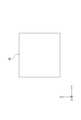
図2は、図1の一対の触覚センサ10の一例を示す斜視図である。一対の触覚センサ10は、一例として、互いに対向する方向に面対称である。X軸方向は、一対の触覚センサ10が対向する方向と直交する第一方向に相当し、Y軸方向は、一対の触覚センサ10が対向する方向と直交する第二方向に相当し、Z軸方向は、一対の触覚センサ10が対向する方向に相当する。X軸方向は、Y軸方向と直交している。一例として、X軸方向は、触覚センサ10の縦方向に相当し、Y軸方向は、触覚センサ10の横方向に相当する。 FIG. 2 is a perspective view showing an example of the pair of
触覚センサ10は、支持プレート14と、基板16と、センサ部18とを備える。支持プレート14は、上述の把持部114(図1参照)と別体に構成されており、把持部114に固定される。支持プレート14は、把持部114と一体に構成されていてもよい。基板16は、支持プレート14に固定されており、センサ部18は、基板16上に設けられている。センサ部18の詳細については、後に詳述する。 The
続いて、触覚センシングシステム1の第一乃至第四実施形態を説明する。 Subsequently, the first to fourth embodiments of the
[第一実施形態]
はじめに、第一実施形態を説明する。[First Embodiment]
First, the first embodiment will be described.
(触覚センサ10の構成)
図3は、第一実施形態に係る触覚センサ10の縦断面図である。第一実施形態に係る触覚センサ10は、センサ部18と、基板16とを備える。(Structure of tactile sensor 10)
FIG. 3 is a vertical sectional view of the
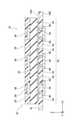
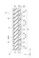
センサ部18は、静電容量方式である。このセンサ部18は、より具体的には、自己容量方式であり、複数の層が積層された積層構造を有する。すなわち、センサ部18は、複数の層として、絶縁層20と、弾力層22と、第一電極層24と、第二電極層26とを有する。第一電極層24及び第二電極層26は、弾力層22を挟んだ両側に位置する。 The
絶縁層20は、第二電極層26に対する弾力層22と反対側に位置する。絶縁層20は、センサ部18の表層部を形成している。この絶縁層20の表面は、ワークW(図1参照)との接触面28として形成されている。なお、絶縁層20は省略されてもよい。絶縁層20が省略された場合には、第二電極層26や第二電極層26の上に形成された表層の表面が接触面28とされる。 The insulating
弾力層22は、誘電体である。弾力層22は、柔軟性及び弾力性を有している。この弾力層22は、例えば、ゲルによって形成される。絶縁層20、弾力層22、第一電極層24及び第二電極層26は、Z軸方向に積層されている。Z軸方向は、接触面28の法線方向に相当する。絶縁層20、弾力層22、第一電極層24及び第二電極層26は、例えば、接着剤等により互いに接着されている。絶縁層20は、センサ部18の全体の接着強度を高めるために、第二電極層26の全面を覆う大きさを有することが好ましい。 The
第一電極層24は、複数の第一電極34を有する。複数の第一電極34は、基板16のセンサ部18側の第一面16Aに形成されている。基板16のセンサ部18と反対側の第二面16Bには、複数の静電容量検出IC(Integrated Circuit)44が実装されている。複数の第一電極34と複数の静電容量検出IC44とは、基板16の板厚方向に延びるスルーホールビア46によって接続されている。 The
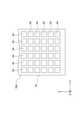
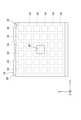
図4は、図3の基板16の平面図である。基板16の第一面16Aに形成された複数の第一電極34は、X-Y平面に沿って行列状に配列されている。つまり、複数の第一電極34は、X軸方向を縦方向とし、Y軸方向を横方向として配列されている。X-Y平面は、上述の接触面28(図2参照)と平行な面である。 FIG. 4 is a plan view of the
複数の第一電極34は、互いに独立している。この複数の第一電極34は、同一の形状である。複数の第一電極34は、一例として、平面視で正方形に形成されている。平面視とはZ軸方向に見ることに相当する。複数の第一電極34は、一例として、X軸方向に6個ずつ、Y軸方向に6個ずつ配列されている。つまり、複数の第一電極34の数は36個である。この複数の第一電極34は、X軸方向及びY軸方向にそれぞれ等間隔に配列されている。 The plurality of
図5は、図3の第二電極層26の平面図である。第二電極層26は、単層である複数の第二電極36によって構成されている。複数の第二電極36は、例えば、導電ゴムによって形成される。この複数の第二電極36は、それぞれ平板状に形成されている。複数の第二電極36は、基板16のグランドに接続されていてもよく、グランドに対して浮いていてもよい。 FIG. 5 is a plan view of the
複数の第二電極36は、互いに独立した複数の島部を形成している。この複数の第二電極36は、X-Y平面に沿って行列状に配列されている。つまり、複数の第二電極36は、X軸方向を縦方向とし、Y軸方向を横方向として配列されている。 The plurality of
複数の第二電極36は、同一の形状である。複数の第二電極36は、一例として、それぞれ平面視で正方形に形成されている。複数の第二電極36の数は、上述の複数の第一電極34(図4参照)の数よりも少ない。この複数の第二電極36は、一例として、X軸方向に3個ずつ、Y軸方向に3個ずつ配列されている。つまり、複数の第二電極36の数は9個である。この複数の第二電極36は、X軸方向及びY軸方向にそれぞれ等間隔に配列されている。 The plurality of
図6は、図3の複数の第二電極36と弾力層22と基板16とを重ねた状態を示す平面図である。複数の第二電極36は、平面視で複数の第一電極34の全てと重なるように配置されている。複数の第二電極36のそれぞれは、平面視で複数の第一電極34のうちX軸方向及びY軸方向に隣接する4個の第一電極34のそれぞれと部分的に重なるように形成されている。各第二電極36は、平面視で4個の第一電極34の中心部に位置し、この4個の第一電極34と部分的に重なっている。 FIG. 6 is a plan view showing a state in which the plurality of
このように、第一実施形態では、複数の第一電極34の全てが複数の第二電極36と部分的に重なっている。この第一実施形態では、複数の第一電極34の全てが、「複数の第二電極と部分的に重なる複数の部分重畳電極」の一例に相当し、複数の第一電極34から出力される複数の信号は、「複数の部分重複電極信号」の一例に相当する。 As described above, in the first embodiment, all of the plurality of
第一実施形態では、複数の第一電極34の全てが、「第二電極と部分的に重なる複数の部分重複電極」の一例に相当し、複数の第一電極34から出力される複数の信号は、「複数の部分重複電極信号」の一例に相当する。 In the first embodiment, all of the plurality of
第一電極34と第二電極36との間の静電容量C[F]は、次式によって求められる。
C=ε×A/d
εは弾力層22の誘電定数[Fm-1]であり、Aは第一電極34と第二電極36の平面視で重なり合う面積[m2]であり、dはZ軸方向に沿った第一電極34と第二電極36との間の距離[m]である。The capacitance C [F] between the
C = ε × A / d
ε is the dielectric constant [Fm-1 ] of the
このセンサ部18では、接触面28に圧力が加わり、各第一電極34と第二電極36との間の距離dが変化すると、この距離dの変化に応じて静電容量Cが変化する。また、センサ部18では、接触面28にせん断力が加わり、各第一電極34と第二電極36の重なり合う面積Aが変化すると、この面積Aの変化に応じて静電容量Cが変化する。 In the
なお、後に詳述するが、接触面28に加わる圧力とは、Z軸方向に沿って接触面28に加わる力に相当する。また、接触面28に加わるせん断力とは、Z軸方向と直交する方向に沿って接触面28に加わる力に相当する。Z軸方向と直交する方向には、X軸方向、Y軸方向、及び、X軸方向とY軸方向とを組み合わせた方向がある。 As will be described in detail later, the pressure applied to the
複数の第一電極34は、後述する静電容量検出IC44(図3、図7参照)によって駆動され、第二電極36との間の静電容量Cに応じた信号をそれぞれ出力する。つまり、センサ部18は、複数の第一電極34のそれぞれに対応する複数の信号を出力する。この複数の信号は、アナログ信号である。 The plurality of
図7は、図3の基板16の底面図である。複数の静電容量検出IC44は、X-Y平面に沿って行列状に配列されている。つまり、複数の静電容量検出IC44は、X軸方向を縦方向とし、Y軸方向を横方向として配列されている。複数の静電容量検出IC44は、同一の構成である。複数の静電容量検出IC44は、一例として、X軸方向に3個ずつ、Y軸方向に3個ずつ配列されている。つまり、複数の静電容量検出IC44の数は9個である。 FIG. 7 is a bottom view of the
各静電容量検出IC44には、この静電容量検出ICと平面視で重なる4個の第一電極34が接続されている。各静電容量検出IC44は、4個の第一電極34を駆動し、この4個の第一電極34から出力された信号に応じたデータを出力可能な構成である。 Each
(触覚センサ10の製造方法)
図8は、図3の触覚センサ10の製造方法の一例を説明する図である。触覚センサ10は、例えば、次の要領で製造される。すなわち、複数の第一電極34がパターンによって第一面16Aに形成された基板16の第二面16Bに複数の静電容量検出IC44が実装される。基板16には、複数のスルーホールビア46が形成されており、複数の静電容量検出IC44は、複数のスルーホールビア46を介して複数の第一電極34と接続される。(Manufacturing method of tactile sensor 10)
FIG. 8 is a diagram illustrating an example of a method for manufacturing the
続いて、複数の第一電極34を有する第一電極層24の上に弾力層22が積層される。また、弾力層22の上に、複数の第二電極36(図5参照)によって構成された第二電極層26が積層され、さらに、この第二電極層26の上に、絶縁層20が積層される。絶縁層20、弾力層22、第一電極層24及び第二電極層26は、例えば、接着剤等により互いに接着される。以上の要領で、触覚センサ10は製造される。 Subsequently, the
なお、図5に示されるように、第二電極36に複数の開口38を形成する加工方法としては、抜き加工、切削加工、注型成形及び金型プレス成形等が挙げられる。 As shown in FIG. 5, examples of the processing method for forming a plurality of
(変位Δx、Δy、Δzの説明)
図9は、図3の触覚センサ10における変位Δxと変位Δyの一例を説明する平面図である。なお、図9では、複数の第一電極34のそれぞれと第二電極36との間の静電容量C00~C55が複数の第一電極34のそれぞれに対応して示されている。(Explanation of displacement Δx, Δy, Δz)
FIG. 9 is a plan view illustrating an example of the displacement Δx and the displacement Δy in the
図10は、図3の触覚センサ10における変位Δxと変位Δzの一例を説明する図である。図10には、(A)垂直荷重Fz’なし、(B)垂直荷重Fz’あり、(C)せん断力Fxあり、(D)垂直荷重Fz’あり+せん断力Fxありの場合がそれぞれ示されている。 FIG. 10 is a diagram illustrating an example of displacement Δx and displacement Δz in the
図11は、図3の触覚センサ10における変位Δyと変位Δzの一例を説明する図である。図11には、(A)垂直荷重Fz’なし、(B)垂直荷重Fz’あり、(C)せん断力Fyあり、(D)垂直荷重Fz’あり+せん断力Fyありの場合がそれぞれ示されている。 FIG. 11 is a diagram illustrating an example of the displacement Δy and the displacement Δz in the
図9、図10に示されるように、変位Δxは、せん断力Fxが作用することに伴って第二電極36がX軸方向に沿って移動した距離に相当する。同様に、図9、図11に示されるように、変位Δyは、せん断力Fyが作用することに伴って第二電極36がY軸方向に沿って移動した距離に相当する。 As shown in FIGS. 9 and 10, the displacement Δx corresponds to the distance that the
図10、図11に示されるように、距離Z0は、垂直荷重Fz’が作用していないときの第一電極34と第二電極36との間のZ軸方向に沿った距離に相当する。変位Δzは、垂直荷重Fz’が作用することに伴って第二電極36がZ軸方向に沿って第一電極34側に移動した距離に相当する。As shown in FIGS. 10 and 11, the distance Z0 corresponds to the distance along the Z-axis direction between the
以下、1つの第二電極36と部分的に重なる隣り合わせの第一電極34を例に変位Δx、Δy、Δzの計算例を説明する。 Hereinafter, a calculation example of the displacements Δx, Δy, and Δz will be described by taking as an example an adjacent
(垂直荷重Fz’が作用していないとき:Δx、Δy、Δz=0)
図10(A)、図11(A)に示されるように、垂直荷重Fz’が作用していないときには、Δx、Δy、Δz=0であり、第二電極36と部分的に重なる隣り合わせの第一電極34については、式1が成立する。(When the vertical load Fz'is not acting: Δx, Δy, Δz = 0)
As shown in FIGS. 10 (A) and 11 (A), when the vertical load Fz'is not acting, Δx, Δy, Δz = 0, and the second electrode is adjacent to the
[式1]
C00_0=K1/Z0
C01_0=K2/Z0
C00_0、C01_0は垂直荷重Fz’が作用していないときの隣り合わせの第一電極34と第二電極36との間の静電容量であり、K1、K2は定数である。
他の隣り合わせの第一電極34と第二電極36との間の静電容量についても、式1と同様の式が成立する。[Equation 1]
C00_0 = K1 / Z0
C01_0 = K2 / Z0
C00_0 and C01_0 are the capacitances between the adjacent
The same equation as in
(垂直荷重Fz’のみが作用しているとき:Δx、Δy=0、Δz≠0)
図10(B)、図11(B)に示されるように、垂直荷重Fz’のみが作用しているときには、Δx、Δy=0、Δz≠0であり、第二電極36と部分的に重なる隣り合わせの第一電極34については、式2が成立する。(When only the vertical load Fz'is acting: Δx, Δy = 0, Δz ≠ 0)
As shown in FIGS. 10 (B) and 11 (B), when only the vertical load Fz'is acting, Δx, Δy = 0, Δz ≠ 0, which partially overlaps with the
[式2]
C00_z=K1/(Z0-Δz)
C01_z=K2/(Z0-Δz)
C00_z、C01_zは垂直荷重Fz’のみが作用しているときの隣り合わせの第一電極34と第二電極36との間の静電容量である。[Equation 2]
C00_z = K1 / (Z0 -Δz)
C01_z = K2 / (Z0 -Δz)
C00_z and C01_z are the capacitances between the adjacent
式2より、以下が求まる。
C00_z/K1=1/(Z0-Δz)
Z0-Δz=K1/C00_z
Δz=Z0-K1/C00_zFrom Equation 2, the following can be obtained.
C00_z / K1 = 1 / (Z0 -Δz)
Z0 -Δz = K1 / C00_z
Δz = Z0 −K1 / C00_z
式1より、一方の第一電極34に対する第二電極36の変位Δzについて以下が求まる。
Z0=K1/C00_0
∴Δz=K1(1/C00_0-1/C00_z)
同様に、他方の第一電極34に対する第二電極36の変位Δzについて以下が求まる。
Δz=K2(1/C01_0-1/C01_z)
他の第一電極34に対する第二電極36の変位Δzについても、上記と同様に求まる。From
Z0 = K1 / C00_0
∴Δz = K1 (1 / C00_0 -1 / C00_z )
Similarly, the following can be obtained for the displacement Δz of the
Δz = K2 (1 / C01_0 -1 / C01_z )
The displacement Δz of the
(せん断力Fxのみが作用しているとき:Δy、Δz=0、Δx≠0)
図10(C)に示されるように、せん断力Fxのみが作用しているときには、Δy、Δz=0、Δx≠0であり、第二電極36と部分的に重なる隣り合わせの第一電極34については、式3が成立する。(When only shear force Fx is acting: Δy, Δz = 0, Δx ≠ 0)
As shown in FIG. 10C, when only the shearing force Fx is acting, Δy, Δz = 0, Δx ≠ 0, and the adjacent
[式3]
C00_x=K1/Z0+Δx・Kp/Z0
C01_x=K2/Z0-Δx・Kp/Z0
C00_x、C01_xはせん断力Fxのみが作用しているときのx方向に隣り合わせの第一電極34と第二電極36との間の静電容量であり、Kpは定数である。[Equation 3]
C00_x = K1 / Z0 + Δx · Kp / Z0
C01_x = K2 / Z0 -Δx ・ Kp / Z0
C00_x and C01_x are the capacitances between the
式3より、以下が求まる。
Δx・Kp/Z0=C00_x-K1/Z0
Δx・Kp=Z0・C00_x-K1
Δx=(Z0・C00_x-K1)/Kp
式1より、K1=Z0×C00_0であるため、一方の第一電極34に対する第二電極36の変位Δxについて以下が求まる。
Δx=(Z0・C00_x-Z0×C00_0)/Kp
Δx=Z0/Kp×(C00_x-C00_0)
同様に、他方の第一電極34に対する第二電極36の変位Δxについて以下が求まる。
Δx=Z0/Kp×(C01_0-C01_x)
他の第一電極34に対する第二電極36の変位Δxについても、上記と同様に求まる。From Equation 3, the following can be obtained.
Δx · Kp / Z0 = C00_x −K1 / Z0
Δx ・ Kp = Z0・ C00_x -K1
Δx = (Z0 · C00_x −K1) / Kp
From
Δx = (Z0 · C00_x −Z0 × C00_0 ) / Kp
Δx = Z0 / Kp × (C00_x -C00_0 )
Similarly, the following can be obtained for the displacement Δx of the
Δx = Z0 / Kp × (C01_0 -C01_x )
The displacement Δx of the
(せん断力Fyのみが作用しているとき:Δx、Δz=0、Δy≠0)
図11(C)に示されるように、せん断力Fyのみが作用しているときには、せん断力Fxのみが作用しているときと同様の計算により、第一電極34に対する第二電極36の変位Δyが求まる。(When only the shear force Fy is acting: Δx, Δz = 0, Δy ≠ 0)
As shown in FIG. 11C, when only the shear force Fy is acting, the displacement Δy of the
(垂直荷重Fz’及びせん断力Fxのみが作用しているとき:Δy=0、Δx、Δz≠0)
図10(D)に示されるように、垂直荷重Fz’及びせん断力Fxのみが作用しているときには、Δy=0、Δx、Δz≠0であり、第二電極36と部分的に重なる隣り合わせの第一電極34については、式4が成立する。(When only vertical load Fz'and shear force Fx are acting: Δy = 0, Δx, Δz ≠ 0)
As shown in FIG. 10 (D), when only the vertical load Fz'and the shear force Fx are acting, Δy = 0, Δx, Δz ≠ 0, and they are adjacent to each other partially overlapping the
[式4]
C00_zx=K1/(Z0-Δz)+Δx・Kp/(Z0-Δz)
C01_zx=K2/(Z0-Δz)+Δx・Kp/(Z0-Δz)
C00_zx、C01_zxは垂直荷重Fz’及びせん断力Fxのみが作用しているときの第一電極34と第二電極36との間の静電容量である。[Equation 4]
C00_zx = K1 / (Z0 -Δz) + Δx · Kp / (Z0 -Δz)
C01_zx = K2 / (Z0 -Δz) + Δx · Kp / (Z0 -Δz)
C00_zx and C01_zx are the capacitances between the
式4より、第一電極34に対する第二電極36の変位Δz、Δxについて以下が求まる。
Δz=(K1+K2){1/(C00_0+C01_0)-1/(C00_zx+C01_zx)}
Δx=(K1+K2)/2Kp・(C00_zx-C01_zx)/(C00_zx+C01_zx)
他の第一電極34に対する第二電極36の変位Δz、Δxについても、上記と同様に求まる。From Equation 4, the following can be obtained for the displacements Δz and Δx of the
Δz = (K1 + K2) {1 / (C00_0 + C01_0 ) -1 / (C00_zx + C01_zx )}
Δx = (K1 + K2) / 2Kp · (C00_zx -C01_zx ) / (C00_zx + C01_zx )
The displacements Δz and Δx of the
(垂直荷重Fz’及びせん断力Fyのみが作用しているとき:Δx=0、Δy、Δz≠0)
図11(D)に示されるように、垂直荷重Fz’及びせん断力Fyのみが作用しているときには、垂直荷重Fz’及びせん断力Fxのみが作用しているときと同様の計算により、隣り合わせの第一電極34に対する第二電極36の変位Δz、Δyが求まる。(When only the vertical load Fz'and the shear force Fy are acting: Δx = 0, Δy, Δz ≠ 0)
As shown in FIG. 11 (D), when only the vertical load Fz'and the shear force Fy are acting, they are adjacent to each other by the same calculation as when only the vertical load Fz'and the shearing force Fx are acting. The displacements Δz and Δy of the
(垂直荷重Fz’及びせん断力Fx、Fyが作用しているとき:Δx、Δy、Δz≠0)
垂直荷重Fz’及びせん断力Fx、Fyが作用しているときには、第一電極34に対する第二電極36の変位Δx、Δy、Δzを次のようにして求めることができる。1つの第二電極36と部分的に重なる4つの第一電極34の範囲では、各第一電極34における変位Δzの値は互いに近似している場合が多いので、変位Δzの値は共通であると仮定する。その場合、各第一電極34に対応する信号の大きさ(静電容量値)は、各第一電極34の第二電極36との重なり面積に比例する。よって、静電容量値C00、C01、C10、C11の比は、重なり面積S00、S01、S10、S11の比と等しい。すなわち、式5が成立する。
[式5]
C00:C01:C10:C11=S00:S01:S10:S11(When vertical load Fz'and shear forces Fx and Fy are acting: Δx, Δy, Δz ≠ 0)
When the vertical load Fz'and the shear forces Fx and Fy are acting, the displacements Δx, Δy and Δz of the
[Equation 5]
C00 : C01 : C10 : C11 = S00 : S01 : S10 : S11
重なり面積S00、S01、S10、S11は、無負荷状態での重なり面積の平方根をaとすると、式6で表される。
[式6]
S00=(a-Δx)×(a-Δy)、S01=(a-Δx)×(a+Δy)、S10=(a+Δx)×(a-Δy)、S11=(a+Δx)×(a+Δy)The overlapping areas S00 , S01 , S10 and S11 are expressed by the equation 6 where the square root of the overlapping area in the no-load state is a.
[Equation 6]
S00 = (a-Δx) × (a-Δy), S01 = (a-Δx) × (a + Δy), S10 = (a + Δx) × (a-Δy), S11 = (a) + Δx) × (a + Δy)
式6より、4つの重なり面積の和は、4a2となり定数である。したがって、4つの重なり面積の和4a2と式5から重なり面積S00、S01、S10、S11が既知の値となる。以上より、式6の連立方程式により、未知の変位Δx、Δyが算出可能である。From Equation 6, the sum of the four overlapping areas is 4a2 , which is a constant. Therefore, from the sum 4a2 of the four overlapping areas and the equation 5, the overlapping areas S00 , S01 , S10 and S11 are known values. From the above, unknown displacements Δx and Δy can be calculated by the simultaneous equations of Equation 6.
変位Δx、Δyを算出したら、それらを既知の値として、共通の値であると仮定した変位Δzを各第一電極34における個別の変位Δzに補正してもよい。この補正は、例えば別の手段で4つの変位Δzの真値が測定できる環境で事前に変位Δx、Δyと4つの変位Δzとの間の相関関係を取得しておいてそれを利用することにより行うことができる。この相関関係の取得を機械学習により行ってもよい。 After the displacements Δx and Δy are calculated, they may be used as known values, and the displacement Δz assumed to be a common value may be corrected to the individual displacement Δz in each
各第一電極34に対応する4つの静電容量値がほぼ等しく、すなわち変位Δx及び変位Δyがゼロに近いことが分かった場合には、上記のΔx、Δy=0、Δz≠0の場合について説明した方法により、4つの第一電極34における変位Δzを個別に算出してもよい。Δx、Δy=0、Δz≠0の場合というのは、例えば台に置かれた状態のワークWを把持していて接触面28にワークWの重量がかかっていない場合である。この状態からワークWを台から持ち上げると、変位Δzはあまり変化しないまま、変位Δx、Δyが主に変化するので、変位Δzを既知の値と扱って変位Δx、Δyをより正確に求めることができる。 When it is found that the four capacitance values corresponding to each
本明細書において、「複数の圧力検出位置のそれぞれの圧力値を算出する」ことは、4つの第一電極34のような複数の圧力検出位置における変位Δzが共通と仮定した場合に、算出した共通の変位Δzに基づく圧力値をそれぞれの圧力検出位置における圧力値として扱うことを含む。また、「複数の圧力検出位置のそれぞれの圧力値について代表値の算出を行うことで集約圧力値を算出する」ことは、4つの第一電極34のような複数の圧力検出位置における変位Δzが共通と仮定した場合に、算出した共通の変位Δzに基づく圧力値を代表値として集約圧力値を算出することを含む。 In the present specification, "calculating the pressure value of each of the plurality of pressure detection positions" is calculated when it is assumed that the displacement Δz at the plurality of pressure detection positions such as the four
以上説明したように、出力部12は、それぞれのせん断力Fx、Fy値を、第二電極36と部分的に重なる第一電極34である少なくとも1つの部分重複電極を含む複数の第一電極34のそれぞれに対応する複数の信号に基づいて、圧力が複数の信号に及ぼす影響を除去するようにして算出する。 As described above, the
次に、第一実施形態の作用及び効果について説明する。 Next, the operation and effect of the first embodiment will be described.
触覚センサ10(図3~図7参照)において、第二電極層26は、単層である複数の第二電極36によって構成されている。したがって、触覚センサ10の構造及び製造工程を簡素化することができる。 In the tactile sensor 10 (see FIGS. 3 to 7), the
また、第一電極34と第二電極36との間の距離に応じて変化する静電容量を検出することにより、複数の第一電極34のそれぞれの位置で圧力を検出できる。さらに、各第二電極36は、X軸方向及びY軸方向に隣接する4個の第一電極34のそれぞれと部分的に重なっているので、この4個の第一電極34と第二電極36の重なり合う面積に応じて変化する静電容量を検出することにより、各第二電極36の位置でせん断力も検出できる。 Further, by detecting the capacitance that changes according to the distance between the
しかも、複数の第二電極36の数が、複数の第一電極34の数よりも少ないことにより、1つの第二電極36に対して複数の第一電極34がマッチングされるので、例えば、複数の第一電極34が複数の第二電極36と1対1にマッチングされる場合に比して、複数の第一電極34の互いの間隔を狭めることができる。これにより、複数の第一電極34の数を確保できるので、圧力分布の分解能を確保できる。 Moreover, since the number of the plurality of
このように、第一実施形態に係る触覚センサ10によれば、簡素な構造及び製造工程でもせん断力を検出できると共に、圧力分布の分解能を確保できる。 As described above, according to the
次に、第一実施形態の変形例について説明する。 Next, a modified example of the first embodiment will be described.
触覚センサ10は、36個の第一電極34を有するが、複数の第一電極34の数は、いくつでもよい。 The
複数の第二電極36の数は、複数の第一電極34の数よりも少なければ、いくつでもよい。 The number of the plurality of
複数の第一電極34は、好ましくは、接触面28に沿って行列状に配列されるが、接触面28内で所望の圧力分布が得られるのであれば、行列状以外の態様で配置されていてもよい。 The plurality of
[第二実施形態]
次に、第二実施形態を説明する。[Second Embodiment]
Next, the second embodiment will be described.
(触覚センサ10の構成)
図12は、第二実施形態に係る触覚センサ10の縦断面図である。第二実施形態に係る触覚センサ10は、上述の第一実施形態に係る触覚センサ10(図3~図6参照)に対し、第二電極層26の構成が次のように変更されている。(Structure of tactile sensor 10)
FIG. 12 is a vertical sectional view of the
図13は、図12の第二電極層26の平面図である。第二電極層26は、単層である1の第二電極36によって構成されている。つまり、第二電極36は、1つの島部を形成している。第二電極36は、例えば、導電ゴムによって形成される。この第二電極36は、平板状に形成されている。第二電極36は、基板16のグランドに接続されていてもよく、グランドに対して浮いていてもよい。 FIG. 13 is a plan view of the
図14は、図12の第二電極36と弾力層22と基板16とを重ねた状態を示す平面図である。一例として、複数の第一電極34の数は36個であるのに対し、第二電極36は、1つの島部を形成するので、第二実施形態では、第二電極36によって形成される島部の数が複数の第一電極34の数よりも少ない。 FIG. 14 is a plan view showing a state in which the
第二電極36は、一例として、接触面28(図12参照)よりも小さい正方形に形成されている。この第二電極36は、平面視で複数の第一電極34の全てと重なる大きさを有している。具体的には、第二電極36は、複数の第一電極34のうち第二電極36の外周部に沿って並ぶ第一電極34と第二電極36の外周部とが平面視で重なる大きさを有している。これにより、第二電極36の外周部に沿って並ぶ第一電極34は、平面視で第二電極36と部分的に重なっており、複数の第一電極34のうち第二電極36の外周部の内側に位置する第一電極34は、第二電極36と全体的に重なっている。 As an example, the
第二実施形態では、複数の第一電極34のうち第二電極36と部分的に重なる第一電極34が、「第二電極と部分的に重なる複数の部分重複電極」の一例に相当し、この第二電極36と部分的に重なる第一電極34から出力される複数の信号は、「複数の部分重複電極信号」の一例に相当する。 In the second embodiment, the
図12に示される触覚センサ10のセンサ部18では、接触面28に圧力が加わり、各第一電極34と第二電極36との間の距離dが変化すると、この距離dの変化に応じて静電容量Cが変化する。また、センサ部18では、接触面28にせん断力が加わり、第二電極36と部分的に重なる第一電極34(図14参照)と第二電極36の重なり合う面積Aが変化すると、この面積Aの変化に応じて静電容量Cが変化する。 In the
このような構成の触覚センサ10は、上述の第一実施形態に係る触覚センサ10(図3~図6参照)と同様に製造される。 The
また、第二実施形態において、変位Δx、Δy、Δzの計算は、第一実施形態の場合と同様の考え方に基づいて行う。 Further, in the second embodiment, the displacements Δx, Δy, and Δz are calculated based on the same concept as in the case of the first embodiment.
次に、第二実施形態の作用及び効果について説明する。 Next, the operation and effect of the second embodiment will be described.
触覚センサ10(図12~図14参照)において、第二電極層26は、単層である1の第二電極36によって構成されている。したがって、触覚センサ10の構造及び製造工程を簡素化することができる。 In the tactile sensor 10 (see FIGS. 12 to 14), the
また、第一電極34と第二電極36との間の距離に応じて変化する静電容量を検出することにより、複数の第一電極34のそれぞれの位置で圧力を検出できる。さらに、複数の第一電極34の一部、すなわち、第二電極36の外周部に沿って並ぶ第一電極34は、平面視で第二電極36と部分的に重なっているので、この第一電極34と第二電極36の重なり合う面積に応じて変化する静電容量を検出することにより、第二電極36の外周部に沿って並ぶ第一電極34の位置でせん断力も検出できる。 Further, by detecting the capacitance that changes according to the distance between the
しかも、第二電極36の数が、1であり、複数の第一電極34の数よりも少ないことにより、1つの第二電極36に対して複数の第一電極34がマッチングされるので、例えば、複数の第一電極34が複数の第二電極36と1対1にマッチングされる場合に比して、複数の第一電極34の互いの間隔を狭めることができる。これにより、複数の第一電極34の数を確保できるので、圧力分布の分解能を確保できる。 Moreover, since the number of the
このように、第二実施形態に係る触覚センサ10によれば、簡素な構造及び製造工程でもせん断力を検出できると共に、圧力分布の分解能を確保できる。 As described above, according to the
また、第二電極36は、単一の構成であるので、例えば、第二電極36が複数の部材によって構成される場合に比して、製造効率を向上させることができると共に、部品点数を削減することができる。 Further, since the
次に、第二実施形態の変形例について説明する。 Next, a modified example of the second embodiment will be described.
触覚センサ10は、36個の第一電極34を有するが、複数の第一電極34の数は、いくつでもよい。 The
第二電極36の数は、1であるが、複数の第一電極34の数よりも少なければ、第二電極36の数は、いくつでもよい。 The number of the
複数の第一電極34は、好ましくは、接触面28に沿って行列状に配列されるが、接触面28内で所望の圧力分布が得られるのであれば、行列状以外の態様で配置されていてもよい。 The plurality of
[第三実施形態]
次に、第三実施形態を説明する。[Third Embodiment]
Next, the third embodiment will be described.
(触覚センサ10の構成)
図15は、第三実施形態に係る触覚センサ10の縦断面図である。第三実施形態に係る触覚センサ10は、上述の第一実施形態に係る触覚センサ10(図3~図6参照)に対し、第二電極層26の構成が次のように変更されている。(Structure of tactile sensor 10)
FIG. 15 is a vertical sectional view of the
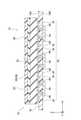
図16は、図15の第二電極層26の平面図である。第二電極層26は、単層である1の第二電極36によって構成されている。第二電極36は、例えば、導電ゴムによって形成される。この第二電極36は、平板状に形成されている。第二電極36は、一例として、平面視で正方形に形成されている。第二電極36は、基板16(図3参照)のグランドに接続されていてもよく、グランドに対して浮いていてもよい。 FIG. 16 is a plan view of the
第二電極36には、複数の開口38が形成されている。複数の開口38は、第二電極36の板厚方向、すなわち、Z軸方向に貫通している。この複数の開口38は、X-Y平面に沿って行列状に配列されている。つまり、複数の開口38は、X軸方向を縦方向とし、Y軸方向を横方向として配列されている。 A plurality of
複数の開口38は、同一の形状である。複数の開口38は、一例として、平面視で正方形に形成されている。複数の開口38の数は、上述の複数の第一電極34(図4参照)の数よりも少ない。複数の開口38は、一例として、X軸方向に3個ずつ、Y軸方向に3個ずつ配列されている。つまり、複数の開口38の数は9個である。この複数の開口38は、X軸方向及びY軸方向にそれぞれ等間隔に配列されている。 The plurality of
図17は、図15の第二電極36と弾力層22と基板16とを重ねた状態を示す平面図である。第二電極36は、平面視で複数の第一電極34の全てと重なる大きさを有している。具体的には、第二電極36は、平面視で第二電極36の外形部の内側に複数の第一電極34の全てが収まる大きさを有している。 FIG. 17 is a plan view showing a state in which the
複数の開口38のそれぞれは、平面視で複数の第一電極34のうちX軸方向及びY軸方向に隣接する4個の第一電極34のそれぞれと部分的に重なるように形成されている。具体的には、各開口38は、平面視で4個の第一電極34の中心部に位置し、この4個の第一電極34と部分的に重なっている。 Each of the plurality of
このように、第三実施形態では、複数の第一電極34の全てが平面視で第二電極36の外形部の内側に収まっており、また、複数の第一電極34の全てが開口38と部分的に重なっている。複数の第一電極34の全てが開口38と部分的に重なることは、複数の第一電極34の全てが第二電極36と部分的に重なることに相当する。 As described above, in the third embodiment, all of the plurality of
第三実施形態では、複数の第一電極34の全てが、「第二電極と部分的に重なる複数の部分重畳電極」の一例に相当し、複数の第一電極34から出力される複数の信号は、「複数の部分重複電極信号」の一例に相当する。 In the third embodiment, all of the plurality of
図15に示される触覚センサ10のセンサ部18では、接触面28に圧力が加わり、各第一電極34と第二電極36との間の距離dが変化すると、この距離dの変化に応じて静電容量Cが変化する。また、センサ部18では、接触面28にせん断力が加わり、各第一電極34と第二電極36の重なり合う面積Aが変化すると、この面積Aの変化に応じて静電容量Cが変化する。 In the
このような構成の触覚センサ10は、上述の第一実施形態に係る触覚センサ10(図3~図6参照)と同様に製造される。 The
また、第三実施形態において、変位Δx、Δy、Δzの計算は、第一実施形態の場合と同様の考え方に基づいて行う。 Further, in the third embodiment, the displacements Δx, Δy, and Δz are calculated based on the same concept as in the case of the first embodiment.
次に、第三実施形態の作用及び効果について説明する。 Next, the operation and effect of the third embodiment will be described.
触覚センサ10(図15~図17参照)において、第二電極層26は、単層である1の第二電極36によって構成されている。したがって、触覚センサ10の構造及び製造工程を簡素化することができる。 In the tactile sensor 10 (see FIGS. 15 to 17), the
また、第一電極34と開口38との間の距離に応じて変化する静電容量を検出することにより、複数の第一電極34のそれぞれの位置で圧力を検出できる。さらに、各開口38は、X軸方向及びY軸方向に隣接する4個の第一電極34のそれぞれと部分的に重なっているので、この4個の第一電極34と複数の開口38の重なり合う面積に応じて変化する静電容量を検出することにより、各開口38の位置でせん断力も検出できる。 Further, by detecting the capacitance that changes depending on the distance between the
しかも、第二電極36に形成された開口38の数が、複数の第一電極34の数よりも少ないことにより、1つの開口38に対して複数の第一電極34がマッチングされるので、例えば、複数の第一電極34が複数の開口38と1対1にマッチングされる場合に比して、複数の第一電極34の互いの間隔を狭めることができる。これにより、複数の第一電極34の数を確保できるので、圧力分布の分解能を確保できる。 Moreover, since the number of
このように、第三実施形態に係る触覚センサ10によれば、簡素な構造及び製造工程でもせん断力を検出できると共に、圧力分布の分解能を確保できる。 As described above, according to the
また、第二電極36は、複数の開口38を有する単一の構成であるので、例えば、第二電極36が複数の部材によって構成される場合に比して、製造効率を向上させることができると共に、部品点数を削減することができる。 Further, since the
触覚センサ10は、36個の第一電極34を有するが、複数の第一電極34の数は、いくつでもよい。 The
複数の第二電極36の数は、複数の第一電極34の数よりも少なければ、いくつでもよい。 The number of the plurality of
複数の第一電極34は、好ましくは、接触面28に沿って行列状に配列されるが、接触面28内で所望の圧力分布が得られるのであれば、行列状以外の態様で配置されていてもよい。 The plurality of
[第四実施形態]
次に、第四実施形態を説明する。[Fourth Embodiment]
Next, a fourth embodiment will be described.
(触覚センサ10の構成)
図18は、第四実施形態に係る触覚センサ10の縦断面図である。第四実施形態に係る触覚センサ10は、上述の第一実施形態に係る触覚センサ10(図3~図6参照)に対し、第二電極層26の構成が次のように変更されている。(Structure of tactile sensor 10)
FIG. 18 is a vertical sectional view of the
図19は、図18の第二電極層26の平面図である。第二電極層26は、単層である1の第二電極36によって構成されている。第二電極36は、平板状に形成されている。この第二電極36は、基板16のグランドに接続されていてもよく、グランドに対して浮いていてもよい。第二電極36は、例えば、導電ゴムによって形成される。 FIG. 19 is a plan view of the
第二電極36には、1つの開口38が形成されている。開口38は、一例として、第二電極36の中央部に形成されている。第二電極36は、平面視で正方形に形成されており、開口38も、平面視で正方形に形成されている。 One
図20は、図18の第二電極36と弾力層22と基板16とを重ねた状態を示す平面図である。一例として、複数の第一電極34の数は36個であるのに対し、第二電極36には、1つの開口38が形成されているので、第四実施形態では、第二電極36に形成された開口38の数が複数の第一電極34の数よりも少ない。 FIG. 20 is a plan view showing a state in which the
第二電極36は、平面視で複数の第一電極34の全てと重なる大きさを有している。具体的には、第二電極36は、平面視で第二電極36の外形部の内側に複数の第一電極34の全てが収まる大きさを有している。 The
開口38は、一例として、平面視でX軸方向及びY軸方向に隣接する中央の4個の第一電極34の全てを収める最小の正方形よりも小さい正方形に形成されている。開口38は、平面視で中央の4個の第一電極34の中心部に位置し、この4個の第一電極34と部分的に重なっている。これにより、複数の第一電極34のうち中央の4個の第一電極34は、平面視で第二電極36と部分的に重なっており、複数の第一電極34のうち中央の4個の第一電極34以外の第一電極34は、第二電極36と全体的に重なっている。 As an example, the
第二実施形態では、複数の第一電極34のうち中央の4個の第一電極34が、「第二電極と部分的に重なる複数の部分重複電極」の一例に相当し、この中央の4個の第一電極から出力される複数の信号は、「複数の部分重複電極信号」の一例に相当する。 In the second embodiment, the four
このような構成の触覚センサ10は、上述の第一実施形態に係る触覚センサ10(図3~図6参照)と同様に製造される。 The
第四実施形態において、変位Δx、Δy、Δzの計算は、第一実施形態の場合と同様の考え方に基づいて行う。 In the fourth embodiment, the displacements Δx, Δy, and Δz are calculated based on the same concept as in the case of the first embodiment.
次に、第四実施形態の作用及び効果について説明する。 Next, the operation and effect of the fourth embodiment will be described.
触覚センサ10(図18~図20参照)において、第二電極層26は、単層である1の第二電極36によって構成されている。したがって、触覚センサ10の構造及び製造工程を簡素化することができる。 In the tactile sensor 10 (see FIGS. 18 to 20), the
また、第一電極34と第二電極36との間の距離に応じて変化する静電容量を検出することにより、複数の第一電極34のそれぞれの位置で圧力を検出できる。さらに、複数の第一電極34のうち中央の4個の第一電極34は、平面視で第二電極36の中央に形成された開口38と部分的に重なっているので、この4個の第一電極34と第二電極36の重なり合う面積に応じて変化する静電容量を検出することにより、開口38の位置でせん断力も検出できる。 Further, by detecting the capacitance that changes according to the distance between the
しかも、第二電極36に形成された開口38の数が、1であり、複数の第一電極34の数よりも少ないことにより、1つの開口38に対して複数の第一電極34がマッチングされるので、例えば、複数の第一電極34が複数の開口38と1対1にマッチングされる場合に比して、複数の第一電極34の互いの間隔を狭めることができる。これにより、複数の第一電極34の数を確保できるので、圧力分布の分解能を確保できる。 Moreover, since the number of
このように、第四実施形態に係る触覚センサ10によれば、簡素な構造及び製造工程でもせん断力を検出できると共に、圧力分布の分解能を確保できる。 As described above, according to the
また、第二電極36は、単一の構成であるので、例えば、第二電極36が複数の部材によって構成される場合に比して、製造効率を向上させることができると共に、部品点数を削減することができる。 Further, since the
次に、第四実施形態の変形例について説明する。 Next, a modified example of the fourth embodiment will be described.
触覚センサ10は、36個の第一電極34を有するが、複数の第一電極34の数は、いくつでもよい。 The
第二電極36には、1つの開口38が形成されているが、開口38の数が、複数の第一電極34の数よりも少なければ、開口38の数は、いくつでもよい。 The
複数の第一電極34は、好ましくは、接触面28に沿って行列状に配列されるが、接触面28内で所望の圧力分布が得られるのであれば、行列状以外の態様で配置されていてもよい。 The plurality of
以上、本願の開示する技術の第一乃至第四実施形態について説明したが、本願の開示する技術は、上記に限定されるものでなく、上記以外にも、その主旨を逸脱しない範囲内において種々変形して実施可能であることは勿論である。 The first to fourth embodiments of the technique disclosed in the present application have been described above, but the technique disclosed in the present application is not limited to the above, and various other techniques are used within a range not deviating from the gist thereof. Of course, it can be modified and implemented.
1…触覚センシングシステム、10…触覚センサ、12…出力部、14…支持プレート、16…基板、16A…第一面、16B…第二面、18…センサ部、20…絶縁層、22…弾力層、24…第一電極層、26…第二電極層、28…接触面、34…第一電極、36…第二電極、38…開口、44…静電容量検出I、46…スルーホールビア、100…ロボットシステム、102…ロボット、104…コントローラ、106…ロボットアーム、108…ロボットハンド、110…関節部、112…手首関節部、114…把持部、114A…対向面、W…ワーク1 ... Tactile sensing system, 10 ... Tactile sensor, 12 ... Output unit, 14 ... Support plate, 16 ... Board, 16A ... First surface, 16B ... Second surface, 18 ... Sensor unit, 20 ... Insulation layer, 22 ... Elasticity Layer, 24 ... first electrode layer, 26 ... second electrode layer, 28 ... contact surface, 34 ... first electrode, 36 ... second electrode, 38 ... opening, 44 ... capacitance detection I, 46 ... through hole via , 100 ... Robot system, 102 ... Robot, 104 ... Controller, 106 ... Robot arm, 108 ... Robot hand, 110 ... Joint part, 112 ... Wrist joint part, 114 ... Grip part, 114A ... Facing surface, W ... Work
Claims (5)
Translated fromJapanese前記第一電極層は、複数の第一電極を有し、
前記第二電極層は、単層である1又は複数の第二電極によって構成され、
前記複数の第一電極のうちの2以上は、前記法線方向に見て前記第二電極と部分的に重なる部分重複電極であり、
1の前記第二電極に形成された1又は複数の開口の数、若しくは、1又は複数の前記第二電極によって形成される1又は複数の島部の数は、前記複数の第一電極の数よりも少ない、
触覚センサ。It has a contact surface with an object and has a laminated structure in which an elastic layer and a first electrode layer and a second electrode layer located on both sides of the elastic layer are laminated in the normal direction of the contact surface. Equipped with a capacitance type sensor unit
The first electrode layer has a plurality of first electrodes and has a plurality of first electrodes.
The second electrode layer is composed of one or a plurality of second electrodes which are a single layer.
Two or more of the plurality of first electrodes are partially overlapping electrodes that partially overlap the second electrode when viewed in the normal direction.
The number of one or more openings formed in one of the second electrodes, or the number of one or more islands formed by one or more of the second electrodes is the number of the plurality of first electrodes. Less than,
Tactile sensor.
複数の前記第二電極のそれぞれは、前記法線方向に見て前記複数の第一電極のうち隣接する第一電極のそれぞれと部分的に重なるように形成されている、
請求項1に記載の触覚センサ。The second electrode layer is composed of a plurality of the second electrodes forming the plurality of islands.
Each of the plurality of second electrodes is formed so as to partially overlap each of the adjacent first electrodes among the plurality of first electrodes when viewed in the normal direction.
The tactile sensor according to claim 1.
複数の前記開口のそれぞれは、前記法線方向に見て前記複数の第一電極のうち隣接する第一電極のそれぞれと部分的に重なるように形成されている、
請求項1に記載の触覚センサ。The second electrode layer is composed of one second electrode having a plurality of openings formed therein.
Each of the plurality of openings is formed so as to partially overlap each of the adjacent first electrodes among the plurality of first electrodes when viewed in the normal direction.
The tactile sensor according to claim 1.
前記複数の部分重複電極のそれぞれは、前記法線方向に見て1の前記第二電極と部分的に重なるように形成されている、
請求項1に記載の触覚センサ。The second electrode layer is composed of one second electrode forming the island portion of one.
Each of the plurality of partially overlapping electrodes is formed so as to partially overlap the second electrode of 1 when viewed in the normal direction.
The tactile sensor according to claim 1.
前記複数の部分重複電極のそれぞれは、前記法線方向に見て1の前記開口と部分的に重なるように形成されている、
請求項1に記載の触覚センサ。The second electrode layer is composed of one second electrode having one opening formed therein.
Each of the plurality of partially overlapping electrodes is formed so as to partially overlap the opening of 1 when viewed in the normal direction.
The tactile sensor according to claim 1.
Priority Applications (6)
| Application Number | Priority Date | Filing Date | Title |
|---|---|---|---|
| JP2020140395AJP7420011B2 (en) | 2020-08-21 | 2020-08-21 | tactile sensor |
| EP21858086.8AEP4202390A4 (en) | 2020-08-21 | 2021-07-15 | TACTILE SENSOR |
| CN202180057537.XACN116157663B (en) | 2020-08-21 | 2021-07-15 | Touch sensor |
| PCT/JP2021/026660WO2022038937A1 (en) | 2020-08-21 | 2021-07-15 | Tactile sensor |
| US18/020,882US20230324242A1 (en) | 2020-08-21 | 2021-07-15 | Tactile Sensor |
| TW110128443ATWI801952B (en) | 2020-08-21 | 2021-08-03 | Tactile sensor |
Applications Claiming Priority (1)
| Application Number | Priority Date | Filing Date | Title |
|---|---|---|---|
| JP2020140395AJP7420011B2 (en) | 2020-08-21 | 2020-08-21 | tactile sensor |
Publications (2)
| Publication Number | Publication Date |
|---|---|
| JP2022035827Atrue JP2022035827A (en) | 2022-03-04 |
| JP7420011B2 JP7420011B2 (en) | 2024-01-23 |
Family
ID=80350310
Family Applications (1)
| Application Number | Title | Priority Date | Filing Date |
|---|---|---|---|
| JP2020140395AActiveJP7420011B2 (en) | 2020-08-21 | 2020-08-21 | tactile sensor |
Country Status (6)
| Country | Link |
|---|---|
| US (1) | US20230324242A1 (en) |
| EP (1) | EP4202390A4 (en) |
| JP (1) | JP7420011B2 (en) |
| CN (1) | CN116157663B (en) |
| TW (1) | TWI801952B (en) |
| WO (1) | WO2022038937A1 (en) |
Families Citing this family (2)
| Publication number | Priority date | Publication date | Assignee | Title |
|---|---|---|---|---|
| JP7581700B2 (en)* | 2020-08-21 | 2024-11-13 | オムロン株式会社 | Tactile Sensing System |
| JP7588372B2 (en)* | 2021-01-05 | 2024-11-22 | 本田技研工業株式会社 | Capacitive Sensor |
Citations (5)
| Publication number | Priority date | Publication date | Assignee | Title |
|---|---|---|---|---|
| JPS53112784A (en)* | 1977-01-21 | 1978-10-02 | Semperit Ag | Condenser for measuring power and method |
| JP2013117458A (en)* | 2011-12-05 | 2013-06-13 | Seiko Epson Corp | Detection device, electronic apparatus, and robot |
| JP2015169532A (en)* | 2014-03-06 | 2015-09-28 | 国立大学法人信州大学 | Sheet sensor system and sheet sensor |
| US20190078946A1 (en)* | 2017-09-11 | 2019-03-14 | Regents Of The University Of Minnesota | Supercapacitor-based sensors with flexible electrolytes |
| JP2019152599A (en)* | 2018-03-06 | 2019-09-12 | アルプスアルパイン株式会社 | Sensor, sensor control method, and control program |
Family Cites Families (23)
| Publication number | Priority date | Publication date | Assignee | Title |
|---|---|---|---|---|
| US5974894A (en)* | 1997-07-14 | 1999-11-02 | Panex Incorporated | Fused silica high pressure sensor |
| KR101209302B1 (en)* | 2011-08-09 | 2012-12-06 | 성균관대학교산학협력단 | Capacitor sensor capable of controlling sensitivity of sensor |
| CN202442824U (en)* | 2012-02-20 | 2012-09-19 | 浙江大学 | Bionic flexible tactile sensor array based on combination of piezoresistive type and capacitive type |
| KR101979680B1 (en)* | 2012-12-05 | 2019-05-20 | 삼성전자주식회사 | Tactile sensor |
| TWI470197B (en)* | 2012-12-20 | 2015-01-21 | Ind Tech Res Inst | Capacitive shear force sensor and method for fabricating thereof |
| CN204924512U (en)* | 2015-04-28 | 2015-12-30 | 衢州学院 | Three -dimensional electric capacity sense of touch sensing array of floating electrode formula |
| KR20170053109A (en)* | 2015-11-05 | 2017-05-15 | 주식회사 모다이노칩 | Pressure Sensor and complex device having the same |
| US20180326456A1 (en)* | 2015-11-06 | 2018-11-15 | Moda-Innochips Co., Ltd. | Pressure sensor, and composite element and electronic device having same |
| JP6280579B2 (en)* | 2016-02-29 | 2018-02-14 | Nissha株式会社 | Pressure detection device |
| KR102553036B1 (en)* | 2016-06-29 | 2023-07-07 | 엘지이노텍 주식회사 | Sensor for detecting pressure |
| JP6654161B2 (en)* | 2016-09-05 | 2020-02-26 | オムロンヘルスケア株式会社 | Force detection device |
| US10267690B2 (en)* | 2016-09-13 | 2019-04-23 | The Board Of Trustees Of The Leland Stanford Junior University | Capacitive force/torque sensor |
| CN106959175B (en)* | 2017-03-21 | 2019-07-19 | 合肥工业大学 | A fully flexible capacitive sliding tactile sensor based on pyramid structure |
| WO2018174164A1 (en)* | 2017-03-23 | 2018-09-27 | パナソニックIpマネジメント株式会社 | Tactile sensor, and tactile sensor unit constituting said tactile sensor |
| CN108680287B (en)* | 2018-03-19 | 2020-06-26 | 北京航空航天大学 | High-sensitivity five-degree-of-freedom array type touch sensor |
| CN109282921B (en)* | 2018-11-08 | 2024-06-21 | 衢州学院 | Metal drop electrode type three-dimensional capacitance touch sensor |
| WO2020097730A1 (en)* | 2018-11-16 | 2020-05-22 | The University Of British Columbia | Deformable sensor for simulating skin and other applications |
| JP7311982B2 (en) | 2019-02-27 | 2023-07-20 | キヤノン株式会社 | How to control printer devices and print settings |
| CN109870254B (en)* | 2019-03-01 | 2020-05-29 | 厦门大学 | A highly sensitive capacitive sliding tactile sensor |
| CN109813466A (en)* | 2019-03-22 | 2019-05-28 | 重庆大学 | Tactile Sensor with Slip Sensing |
| CN114061795A (en)* | 2020-07-31 | 2022-02-18 | 深圳市柔宇科技股份有限公司 | Pressure sensor and preparation method thereof |
| JP7581700B2 (en)* | 2020-08-21 | 2024-11-13 | オムロン株式会社 | Tactile Sensing System |
| JP7560031B2 (en)* | 2021-01-20 | 2024-10-02 | 本田技研工業株式会社 | 3-axis force sensor |
- 2020
- 2020-08-21JPJP2020140395Apatent/JP7420011B2/enactiveActive
- 2021
- 2021-07-15CNCN202180057537.XApatent/CN116157663B/enactiveActive
- 2021-07-15USUS18/020,882patent/US20230324242A1/enactivePending
- 2021-07-15WOPCT/JP2021/026660patent/WO2022038937A1/ennot_activeCeased
- 2021-07-15EPEP21858086.8Apatent/EP4202390A4/enactivePending
- 2021-08-03TWTW110128443Apatent/TWI801952B/enactive
Patent Citations (5)
| Publication number | Priority date | Publication date | Assignee | Title |
|---|---|---|---|---|
| JPS53112784A (en)* | 1977-01-21 | 1978-10-02 | Semperit Ag | Condenser for measuring power and method |
| JP2013117458A (en)* | 2011-12-05 | 2013-06-13 | Seiko Epson Corp | Detection device, electronic apparatus, and robot |
| JP2015169532A (en)* | 2014-03-06 | 2015-09-28 | 国立大学法人信州大学 | Sheet sensor system and sheet sensor |
| US20190078946A1 (en)* | 2017-09-11 | 2019-03-14 | Regents Of The University Of Minnesota | Supercapacitor-based sensors with flexible electrolytes |
| JP2019152599A (en)* | 2018-03-06 | 2019-09-12 | アルプスアルパイン株式会社 | Sensor, sensor control method, and control program |
Also Published As
| Publication number | Publication date |
|---|---|
| EP4202390A4 (en) | 2024-08-07 |
| JP7420011B2 (en) | 2024-01-23 |
| CN116157663B (en) | 2025-06-24 |
| TW202208816A (en) | 2022-03-01 |
| TWI801952B (en) | 2023-05-11 |
| WO2022038937A1 (en) | 2022-02-24 |
| CN116157663A (en) | 2023-05-23 |
| EP4202390A1 (en) | 2023-06-28 |
| US20230324242A1 (en) | 2023-10-12 |
Similar Documents
| Publication | Publication Date | Title |
|---|---|---|
| US10267690B2 (en) | Capacitive force/torque sensor | |
| US20120247226A1 (en) | Sheet-like tactile sensor system | |
| US20080053247A1 (en) | Force sensor chip | |
| KR100913741B1 (en) | Capacitive sensor touch sensing electrode plate with multi-axis touch sensing electrode line, touch screen and touch pad using the same | |
| TWI778736B (en) | Tactile sensing system | |
| TWI801952B (en) | Tactile sensor | |
| JP2014163815A (en) | Force detection device, and robot | |
| US20220214232A1 (en) | Capacitance sensor | |
| CN107256101B (en) | Touch display panel and display device | |
| US11740147B2 (en) | Triaxial force sensor | |
| CN107314852A (en) | A kind of wrist sensor | |
| JPH0663892B2 (en) | Pressure recognition control device | |
| JP6699954B1 (en) | Capacitance detection device | |
| US11994441B2 (en) | Sensor device for environmental perception and/or for reliably gripping and manipulating objects | |
| CN106932123A (en) | A kind of wrist sensor | |
| JP2728569B2 (en) | Distributed tactile sensor | |
| JPH0560269B2 (en) | ||
| TW202215218A (en) | Touch Panel Device and Method for Detection | |
| JP2021096202A (en) | Sensor system | |
| JP2014196923A (en) | Force detection device, robot, electronic component transport device, electronic component inspection device, component processing device, and moving body | |
| JPH0797056B2 (en) | Distributed tactile sensor | |
| JPH0660855B2 (en) | Pressure sensor | |
| JPH0546887B2 (en) | ||
| JPH02223835A (en) | Distribution type pressure sensor |
Legal Events
| Date | Code | Title | Description |
|---|---|---|---|
| A621 | Written request for application examination | Free format text:JAPANESE INTERMEDIATE CODE: A621 Effective date:20230607 | |
| A131 | Notification of reasons for refusal | Free format text:JAPANESE INTERMEDIATE CODE: A131 Effective date:20231107 | |
| A521 | Request for written amendment filed | Free format text:JAPANESE INTERMEDIATE CODE: A523 Effective date:20231129 | |
| TRDD | Decision of grant or rejection written | ||
| A01 | Written decision to grant a patent or to grant a registration (utility model) | Free format text:JAPANESE INTERMEDIATE CODE: A01 Effective date:20231212 | |
| A61 | First payment of annual fees (during grant procedure) | Free format text:JAPANESE INTERMEDIATE CODE: A61 Effective date:20231225 | |
| R150 | Certificate of patent or registration of utility model | Ref document number:7420011 Country of ref document:JP Free format text:JAPANESE INTERMEDIATE CODE: R150 |