JP2022028606A - Spectrophotometer - Google Patents
SpectrophotometerDownload PDFInfo
- Publication number
- JP2022028606A JP2022028606AJP2021100126AJP2021100126AJP2022028606AJP 2022028606 AJP2022028606 AJP 2022028606AJP 2021100126 AJP2021100126 AJP 2021100126AJP 2021100126 AJP2021100126 AJP 2021100126AJP 2022028606 AJP2022028606 AJP 2022028606A
- Authority
- JP
- Japan
- Prior art keywords
- light
- light source
- voltage
- infrared
- linear equation
- Prior art date
- Legal status (The legal status is an assumption and is not a legal conclusion. Google has not performed a legal analysis and makes no representation as to the accuracy of the status listed.)
- Granted
Links
Images


Landscapes
- Spectrometry And Color Measurement (AREA)
Abstract
Description
Translated fromJapanese本発明は、赤外光源を備える分光光度計に関し、より特定的には、当該赤外光源の制御に関する。 The present invention relates to a spectrophotometer including an infrared light source, and more specifically to control of the infrared light source.
従来、赤外光源を備える分光光度計が知られている。たとえば、米国特許第7119904号明細書(特許文献1)には、赤外光源から出射される光の量に応じた信号を出力する光検出器を備えるフ-リエ変換赤外(FTIR:Fourier transform infrared)分光光度計が開示されている。当該分光光度計においては、光検出器から出力される電圧と目標電圧との電圧差に基づいて、赤外光源から出射される光の量が目標光量において一定となるように赤外光源に対してフィードバック制御が行われる。 Conventionally, a spectrophotometer provided with an infrared light source is known. For example, US Pat. No. 7,119,904 (Patent Document 1) includes a Fourier transform infrared (FTIR) including an optical detector that outputs a signal according to the amount of light emitted from an infrared light source. infrared) A spectrophotometer is disclosed. In the spectrophotometer, the amount of light emitted from the infrared light source is constant with respect to the target light source based on the voltage difference between the voltage output from the photodetector and the target voltage. Feedback control is performed.
特許文献1に開示されている分光光度計においては、移動鏡を含む干渉計を制御するために、レーザ光が干渉計に出射される。干渉計内における当該レーザ光の多重反射または散乱によって、当該レーザ光の一部が光検出器に達し得る。また、光検出器の構成要素の物性は、通常、温度特性を有する。赤外光源から出射される赤外光の量が同じでも、当該レーザ光および当該温度特性が外乱となり、光検出器から出力される電圧は変化し得る。そのため、赤外光源からの出射光の量と目標光量との実際の光量差は、当該光を受けた光検出器から出力される電圧と目標電圧との電圧差に対応する光量差から乖離し得る。その結果、当該電圧差に基づくフィードバック制御によっては、赤外光源からの出射光の量を目標光量に近づけることが困難になり得る。 In the spectrophotometer disclosed in
本発明は、このような課題を解決するためになされたものであって、その目的は、赤外光源を備える分光光度計において、当該赤外光源の光量制御の精度を向上させることである。 The present invention has been made to solve such a problem, and an object of the present invention is to improve the accuracy of light quantity control of an infrared light source in a spectrophotometer provided with an infrared light source.
本発明に係る分光光度計は、赤外光源と、干渉計と、第1検出器と、モニタ部とを備える。赤外光源は、赤外波長域の光を含む出射光を出射する。干渉計は、入力される当該出射光に基づいて干渉光を生成する。第1検出器は、干渉計から出力され、試料を透過または試料に反射した干渉光に基づいて生成された光を検出する。モニタ部は、赤外光源の出力を監視する。モニタ部は、第2検出器と、光量制御部とを備える。第2検出器は、出射光の量に応じた信号を出力する。光量制御部は、当該信号に基づいて当該量が目標光量に近づくように赤外光源を制御するように動作可能である。赤外光源は、第1波長域の光、および第1波長域とは異なる第2波長域の光を出射する。第2検出器は、第1光検出素子と、第2光検出素子とを備える。第1光検出素子は、第1波長域の光に応じた第1電圧を光量制御部に出力する。第2光検出素子は、第2波長域の光に応じた第2電圧を光量制御部に出力する。 The spectrophotometer according to the present invention includes an infrared light source, an interferometer, a first detector, and a monitor unit. The infrared light source emits emitted light including light in the infrared wavelength region. The interferometer generates interferometric light based on the input emitted light. The first detector detects the light that is output from the interferometer and is generated based on the interferometric light that has passed through or reflected off the sample. The monitor unit monitors the output of the infrared light source. The monitor unit includes a second detector and a light amount control unit. The second detector outputs a signal according to the amount of emitted light. The light amount control unit can operate so as to control the infrared light source so that the amount approaches the target light amount based on the signal. The infrared light source emits light in the first wavelength region and light in a second wavelength region different from the first wavelength region. The second detector includes a first photodetector and a second photodetector. The first photodetection element outputs a first voltage corresponding to the light in the first wavelength region to the light amount control unit. The second photodetector outputs a second voltage corresponding to the light in the second wavelength region to the light amount control unit.
本発明に係る分光光度計によれば、第1波長域の光に応じた第1電圧および第2波長域の光に応じた第2電圧が第2検出器から光量制御部に出力されることにより、赤外光源の光量制御の精度を向上させることができる。 According to the spectrophotometer according to the present invention, the first voltage corresponding to the light in the first wavelength region and the second voltage corresponding to the light in the second wavelength region are output from the second detector to the light amount control unit. Therefore, the accuracy of controlling the amount of light of the infrared light source can be improved.
以下に、実施の形態について図面を参照して詳細に説明する。なお、以下では図中の同一または相当部分には同一符号を付してその説明は原則的に繰返さない。また、以下では、フ-リエ変換赤外分光光度計を単にFTIRと称する。 Hereinafter, embodiments will be described in detail with reference to the drawings. In the following, the same or corresponding parts in the figure are designated by the same reference numerals, and the explanation is not repeated in principle. Further, in the following, the Fourier transform infrared spectrophotometer is simply referred to as FTIR.
図1は、実施の形態に係る分光光度計の一例であるFTIR100の概略構成図である。図1において、X軸、Y軸、およびZ軸は互いに直交している。 FIG. 1 is a schematic configuration diagram of FTIR100, which is an example of a spectrophotometer according to an embodiment. In FIG. 1, the X-axis, Y-axis, and Z-axis are orthogonal to each other.
図1に示されるように、FTIR100は、赤外光源10と、モニタ部1と、コリメートミラー21と、ミラー22,23と、干渉計3と、試料室4と、光検出器5(第1検出器)と、レーザ光源6(単色光源)と、光検出器60と、ミラー61,62,63とを備える。 As shown in FIG. 1, the FTIR 100 includes an
赤外光源10は、赤外波長域の光(赤外光)を含む出射光を出射する。モニタ部1は、光検出器11(第2検出器)と、光量制御部12とを含む。モニタ部1は、赤外光源10の出力を監視する。 The
干渉計3は、赤外光源10から入力される出射光に基づいて赤外干渉光を生成する。干渉計3は、たとえばマイケルソン型干渉計であり、移動鏡31と、ビームスプリッタ(ハーフミラー)32と、固定鏡33とを含む。移動鏡31は、駆動機構を有し、X軸方向に直線的に移動可能である。固定鏡33は、Z軸に平行な回転軸を中心として回転可能に構成され、移動鏡31の移動に追随するように回転角度が制御される。 The
試料室4内には、試料40が配置されている。FTIR100においては、赤外光源10から出射される赤外光が干渉計3に導かれ、干渉計3からの赤外干渉光が試料40を介して光検出器5に導かれる。光検出器5は、試料40を透過した赤外干渉光に基づいて生成された光を検出する。試料40に反射した赤外干渉光に基づいて生成された光を光検出器5が検出するようにFTIR100が構成されてもよい。 A
なお、FTIR100は、光検出器5,60からの信号を受けて分析を行うとともに、FTIR100の統合的な制御を行なう不図示の制御装置を備える。光量制御部12は、当該制御装置の一部として形成されてもよい。 The FTIR 100 includes a control device (not shown) that receives signals from the
赤外光源10は、たとえばグローバー光源であり、高温の赤外素子からの黒体輻射を利用した熱光源である。赤外素子は、たとえばSiCまたはSiNなどのセラミックに電熱線が埋め込まれて成形される。電流が赤外素子を流れることによって赤外素子が1000K~1500Kに加熱されて、赤外光を含む輻射光(出射光)が赤外素子から発生して赤外光源10から出射される。温度Tの赤外素子から発生する波長λの光の強度(輻射スペクトル)B(λ,T)は、以下の式(1)に示されるプランクの輻射公式によって表される。なお、式(1)において、hはプランク定数であり、cは光速であり、kはボルツマン定数である。 The

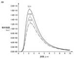
図2は、赤外光源10から出射される輻射光のスペクトルである。図2において、曲線C11は、温度T1における輻射スペクトルB(λ,T1)を表す。曲線C12は、温度T2(<T1)における輻射スペクトルB(λ,T2)を表す。曲線C13は、温度T3(<T2)輻射スペクトルB(λ,T3)を表す。図2に示されるように、輻射スペクトルB(λ,T1)~B(λ,T3)の各々は、赤外領域(0.78μm~1000μm)に含まれる2μm~3μmの波長域において強度のピーク(最大値)を有する。FIG. 2 is a spectrum of synchrotron radiation emitted from the infrared
なお、分析に用いる赤外光の波長域に応じて、赤外光源が切り替えられてもよい。たとえば、当該波長域が近赤外領域(0.78μm~2μm)の場合には赤外光源がハロゲン光源に切り替えられ、当該波長域が中赤外領域(2μm~4μm)および遠赤外領域(4μm~1000μm)の場合には赤外光源がセラミック光源に切り替えられてもよい。 The infrared light source may be switched according to the wavelength range of the infrared light used for the analysis. For example, when the wavelength region is in the near infrared region (0.78 μm to 2 μm), the infrared light source is switched to the halogen light source, and the wavelength region is in the mid-infrared region (2 μm to 4 μm) and the far infrared region (2 μm to 4 μm). In the case of 4 μm to 1000 μm), the infrared light source may be switched to a ceramic light source.
再び図1を参照して、光検出器11は、赤外光源10から出射される輻射光を受けて、当該輻射光の量に応じた信号を光量制御部12に出力する。光量制御部12は、当該信号に基づいて、赤外光源10から出射される輻射光の量が目標光量に近づくように赤外光源10に対してフィードバック制御を行うように動作可能である。 With reference to FIG. 1 again, the
赤外光源10から拡散する光束として出射された赤外光は、コリメートミラー21によって平行な光束(コリメート光)に変換されてビームスプリッタ32に導かれる。赤外光源10から出射される赤外光が収束されてから、アパーチャを介してコリメートミラー21に導かれてもよい。 The infrared light emitted as a luminous flux diffused from the infrared
ビームスプリッタ32に導かれた赤外光は、ビームスプリッタ32によって、移動鏡31に向かう赤外光と固定鏡33に向かう赤外光に分割される。移動鏡31からの反射光と固定鏡33からの反射光とがビームスプリッタ32において干渉することにより、赤外干渉光が干渉計3から出力される。赤外干渉光の強度(振幅)は、移動鏡31の移動によって変化する。 The infrared light guided to the
レーザ光源6は、干渉計3を制御するためのHeNeレーザ光(単色光)を出射する。HeNeレーザ光の波長は、632.8nmである。レーザ光源6から出射されたHeNeレーザ光は、ミラー61を通過した後、ミラー62,63に反射されてビームスプリッタ32に導かれる。ビームスプリッタ32に導かれたHeNeレーザ光は、ビームスプリッタ32によって移動鏡31に向かうHeNeレーザ光と固定鏡33に向かうHeNeレーザ光に分割される。移動鏡31からの反射光と固定鏡33からの反射光とがビームスプリッタ32において干渉することにより、レーザ干渉光が発生する。ビームスプリッタ32からのレーザ干渉光は、ミラー63,62,61によって光検出器60に導かれる。移動鏡31が一定速度で移動する場合、レーザ干渉光の強度は一定周波数の正弦波であるレーザ光干渉縞信号として検出される。当該干渉縞信号に基づいて移動鏡31の位置おおよび速度、ならびに固定鏡33の角度が制御される。なお、レーザ光源6から出射される単色光は、HeNeレーザ光に限定されない。 The
干渉計3から出力された赤外干渉光は、ミラー22によって試料40に収束される。試料40を通過した赤外干渉光は、ミラー23によって光検出器5に収束される。光検出器5によって検出された赤外干渉光の強度信号に基づいて、インターフェログラムが作成される。インターフェログラムにおいては、通常、赤外干渉光の強度が縦軸とされ、移動鏡31からの反射光と固定鏡33からの反射光との光路差が横軸とされる。インターフェログラムにおいては、光路差が0の場合に赤外干渉光の強度のピークが生じる。インターフェログラムをフーリエ変換することにより、強度を縦軸とし、波数(または波長)を横軸とするパワースペクトルが作成される。赤外干渉光を試料40に照射したときに得られるパワースペクトルを、試料40の無い状態で得られるバックグラウンドのパワースペクトルで除することにより、試料40の反射率スペクトルまたは透過率スペクトルが得られる。こられのスペクトルからは、試料40に特有のピーク情報が得られる。 The infrared interference light output from the
次に、FTIR100における赤外光源10のフィードバック制御において解決される課題を説明するため、図3を用いて、モニタ部1の比較例について説明する。 Next, in order to explain the problem solved in the feedback control of the infrared
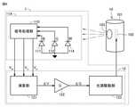
図3は、比較例に係るモニタ部9の構成を示す図である。図3の赤外光源10は、図1に示される赤外光源10に対応する。図3に示されるように、モニタ部9は、光検出器91と、光量制御部92とを含む。赤外光源10は、ケース101と、赤外素子102とを含む。ケース101の側面には、開口部103が形成されている。赤外素子102は、ケース101に収容されている。赤外素子102に光量制御部92から電力が供給されることにより、赤外素子102が発熱し、赤外素子102から赤外光を含む輻射光が発生する。当該輻射光は、開口部103から出射される。 FIG. 3 is a diagram showing the configuration of the
光検出器91は、光検出素子911と、信号処理部910とを含む。光検出素子911は、赤外光源10からの出射光の特定の波長域に対して受光感度を有する。光検出素子911は、当該波長域(感度波長域)に含まれる光に応じた電圧Vを信号処理部910を介して光量制御部92に出力する。光検出素子911としては、たとえば、近赤外領域に受光感度を有するInGaAs型のフォトダイオード、可視領域(380nm~780nm)に受光感度を有するSiPIN型のフォトダイオード、あるいはカラーセンサを挙げることができる。信号処理部910は、光検出素子911からの信号に所定の処理(たとえばAD(Analog-to-Digital)変換)を行って電圧Vに対応する信号を出力する。 The
光量制御部92は、ゲインGを有する差動増幅部922と、光源駆動部123とを含む。差動増幅部922は、電圧Vと目標電圧V0との電圧差ΔVdを増幅して光源駆動部123に信号ΔGd(=G・ΔVd)を出力する。光源駆動部123は、電圧差ΔVdが0となるように赤外光源10に電力を供給する。光源駆動部123は、たとえば、DAコンバータと、差動増幅器と、電圧-電流変換回路と、電流検出抵抗と、フィードバック回路とを含む。電圧-電流変換回路は、トランジスタまたはMOSFET(Metal-Oxide-Semiconductor Field Effect Transistor)を含む。電圧-電流変換回路に替えてPWM(Pulse Width Modulation)変調回路およびブリッジ回路が用いられてもよい。フィードバック回路は、電流検出抵抗によって検出された電流の電圧を差増増幅器へ負帰還する。差動増幅部922は、たとえばファームウェア、またはFPGA(Field Programmable Gate Array)によって実現される。The light
光検出素子911の温度係数をΔβとし、光検出器91の温度と基準温度(たとえばFTIR100起動時の光検出器91の温度)との温度差をΔTaとし、赤外光源10からの出射光の量と目標光量との差に対応する電圧差をΔVとすると、電圧Vは、以下の式(2)のように表される。The temperature coefficient of the

光検出器91の温度がTaで安定している恒温環境における電圧Vの測定値VTaと、光検出器91の温度がTb(=Ta+ΔTa0)で安定している恒温環境における電圧Vの測定値VTbとを用いて、温度係数Δβは以下の式(3)のように表される。The measured value VTa of the voltage V in a constant temperature environment where the temperature of the

目標電圧V0は、赤外光源10からの出射光の目標光量に対応する電圧として、理論的な分析および実機実験によって予め定められた値である。目標電圧V0は、赤外素子102の温度Tが1000K~1500Kの範囲の或る温度となるように定められる。目標電圧V0は、このように予め定められた複数の値からユーザによって選択されてもよいし、ユーザによって変更可能であってもよい。目標電圧V0の近傍の電圧Vにおいては、目標電圧V0と温度Tとの関係は以下の式(4)のような線形式として表される。The target voltage V0 is a voltage corresponding to the target amount of light emitted from the infrared

式(4)において、係数pおよび定数項qの各々は、FTIR100における光検出器91と赤外光源10との位置関係等によって定まるFTIR100に固有の装置定数である。係数pおよび定数項qは、光検出器91および赤外光源10の周囲の温度が一定の恒温環境において予め測定された既知の値である。 In the equation (4), each of the coefficient p and the constant term q is a device constant unique to the
式(2)より、電圧Vと目標電圧V0との単なる電圧差ΔVd(=V-V0)は、以下の式(5)のように表される。From the equation (2), the simple voltage difference ΔVd (= V−V0 ) between the voltage V and the target voltage V0 is expressed by the following equation (5).

式(5)より、電圧差ΔVdには、電圧差ΔVに加えて、光検出素子911の温度特性に由来する値が含まれる。電圧差ΔVdは電圧差ΔVとは異なるため、電圧差ΔVdに基づくフィードバック制御によっては、赤外光源10からの出射光の量を目標光量に近づけることが困難である。赤外光源10の光量制御の精度を向上させるためには、電圧差ΔVに基づいてフィードバック制御を行なう必要がある。式(2)から電圧差ΔVを求めるには、温度差ΔTaを求める必要がある。しかし、FTIR100が稼働している実際の環境は恒温環境ではないため、光検出器91の温度差ΔTaをリアルタイムに取得することは困難である。温度差ΔTaが未知である場合、式(2)からは電圧差ΔVを算出することができない。From the equation (5), the voltage difference ΔVd includes a value derived from the temperature characteristic of the
そこで、FTIR100においては、感度波長域が互いに異なる複数のフォトダイオードからそれぞれ出力される複数の電圧を用いて、電圧差ΔVおよび温度差ΔTaを未知数とする2つ以上の二元一次方程式を連立する。2つの二元一次方程式を用いることにより温度差ΔTaを消去することができるため、電圧差ΔVを導出することができる。FTIR100によれば、赤外光源10からの出射光の量と目標光量との差に対応する電圧差ΔVに基づくフィードバック制御が可能になるため、赤外光源10の光量制御の精度を向上させることができる。Therefore, in the
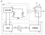
図4は、実施の形態に係るモニタ部1の構成を示す図である。図4において、赤外光源10および光源駆動部123は、図3に示される赤外光源10および光源駆動部123と同様である。 FIG. 4 is a diagram showing the configuration of the
図4に示されるように、光検出器11は、光検出素子111(第1光検出素子)と、光検出素子112(第2光検出素子)と、光検出素子113と、光検出素子114(第3光検出素子)と、信号処理部110とを含む。光量制御部12は、演算部121と、ゲインGを有する増幅部122と、光源駆動部123とを含む。 As shown in FIG. 4, the
光検出素子111~114は、図5に示されるような波長域WB1(400nm~540nm),波長域WB2(450nm~630nm),波長域WB3(575nm~660nm),波長域WB4(785nm~885nm)に対してそれぞれ受光感度を有する。なお、図5の曲線C1は、図2の曲線C11に対応する赤外光源10からの出射光のスペクトルである。 The
図4および図5を参照して、光検出素子111は、波長域WB1に含まれる光に応じた電圧VBを信号処理部110を介して演算部121に出力する。光検出素子112は、波長域WB2に含まれる光に応じた電圧VGを信号処理部110を介して演算部121に出力する。光検出素子113は、波長域WB3に含まれる光に応じた電圧VRを信号処理部110を介して演算部121に出力する。光検出素子114は、波長域WB4に含まれる光に応じた電圧VIRを信号処理部110を介して演算部121に出力する。信号処理部110は、光検出素子111~114からの信号に所定の処理(たとえばAD変換)を行って電圧VB,VG,VR,VIRに対応する信号を演算部121に出力する。信号処理部110は、たとえば、ADコンバータを含む。With reference to FIGS. 4 and 5, the
演算部121は、電圧VB,VG,VR,VIRから電圧差ΔVを算出して、電圧差ΔVを増幅部122に出力する。増幅部122は、電圧差ΔVを増幅して光源駆動部123に信号ΔG(=G・ΔV)を出力する。光源駆動部123は、電圧差ΔVが0となるように赤外光源10に電力を供給する。The
演算部121および増幅部122は、たとえばファームウェア、またはFPGAによって実現される。演算部121は、たとえば、プログラム言語またはハードウェア記述言語により構築される減算器を含む。増幅部122は、たとえば、デジタル値を増幅する構成として、プログラム言語またはハードウェア記述言語により構築される増幅器を含む。増幅部122は、デジタル値をアナログ値に変換するDA(Digital-to-Analog)コンバータと、当該アナログ値を増幅するオペアンプを含んでもよい。なお、増幅部122がアナログ値を出力する場合、光源駆動部123はDAコンバータを含んでいる必要はない。演算部121および増幅部122は、メモリに保存されたプログラムを実行するCPU(Central Processing Unit)等のプロセッサによって実現されてもよい。以下では、演算部121によって行われる電圧差ΔVの導出過程について説明する。 The
電圧VB,VG,VR,VIRの各々は、式(2)に示される電圧Vと同様に、以下の(6)のように表される。Each of the voltages VB , VG ,VR , and VIR is expressed as shown in (6) below, similarly to the voltage V represented by the equation (2).

なお、式(6)は、以下の式(7A),(7B),(7C),(7D)がまとめられた式である。 The formula (6) is a combination of the following formulas (7A), (7B), (7C), and (7D).

以下では、式(7A)~(7D)のように、添え字以外が同型の複数の式は、式(6)のようにまとめて表現される。 In the following, a plurality of expressions having the same type other than the subscripts, such as the expressions (7A) to (7D), are collectively expressed as the expression (6).
式(6)において、電圧VB0,VG0,VR0,VIR0は、赤外光源10からの出射光の目標光量に対応する光検出素子111~114のそれぞれの目標電圧である。電圧差ΔVB,ΔVG,ΔVR,ΔVIRは、赤外光源10からの出射光の量と目標光量との差に対応する光検出素子111~114のそれぞれの電圧差である。温度係数ΔβB,ΔβG,ΔβR,ΔβIRは、光検出素子111~114のそれぞれの温度係数である。温度差ΔTaは、式(2)の温度差ΔTaと同様である。In the formula (6), the voltages VB0 ,VG0 ,VR0 , andVIR0 are the target voltages of the
目標電圧VB0,VG0,VR0,VIR0は、光検出素子111~114のそれぞれのバンドゲインχB,χG,χR,χIRおよび目標電圧V0を用いて、以下の式(8)のように表される。The target voltage VB0 , VG0 , VR0 ,

また、電圧差ΔVB,ΔVG,ΔVR,ΔVIRも、バンドゲインχB,χG,χR,χIRおよび電圧差ΔVを用いて、以下の式(9)のように表される。Further, the voltage difference ΔVB ,ΔVG ,ΔVR , and ΔVIR are also expressed by the following equation (9) using the band gains χB , χG , χR , χIR , and the voltage difference ΔV. ..

目標電圧VB0,VG0,VR0,VIR0のそれぞれの近傍の電圧VB,VG,VR,VIRにおいて、バンドゲインχB,χG,χR,χIRは、一定であり、予め算出されている。The band gains χB , χG , χR , and χIR are constant at the voltages VB , VG ,VR , and VIR in the vicinity of the target voltages VB 0 , VG 0 , VR0 , and
温度係数ΔβB,ΔβG,ΔβR,ΔβIRは、式(3)と同様に、以下の式(10)のように表される。The temperature coefficients ΔβB , ΔβG , ΔβR , and ΔβIR are expressed by the following equation (10), similarly to the equation (3).

式(10)において、電圧VB_Ta,VG_Ta,VR_Ta,VIR_Taは、光検出器11の温度がTaで安定している恒温環境における電圧VB,VG,VR,VIRのそれぞれの測定値である。電圧VB_Tb,VG_Tb,VR_Tb,VIR_Tbは、光検出器11の温度がTbで安定している恒温環境における電圧VB,VG,VR,VIRのそれぞれの測定値である。In equation (10), the voltages VB_Ta , VG_Ta ,VR_Ta , VIR_Ta are the voltages VB , VG ,VR , VIR ina constant temperature environment in which the temperature of the
目標電圧VB0,VG0,VR0,VIR0のそれぞれの近傍の電圧VB,VG,VR,VIRにおいては、電圧VB,VG,VR,VIRと赤外素子102の温度Tとの関係は、式(4)と同様に、以下の式(11)のような線形式として表される。In the voltage VB , VG , VR , VIR in the vicinity of the target voltage VB 0 , VG 0 , VR 0 ,

式(11)において、係数pB,pG,pR,pIRおよび定数項qB,qG,qR,qIRの各々は、FTIR100における光検出器11と赤外光源10との位置関係等によって定まるFTIR100に固有の装置定数である。係数pB,pG,pR,pIRおよび定数項qB,qG,qR,qIRは、光検出器11および赤外光源10の周囲の温度が一定の恒温環境において予め測定された既知の値である。In equation (11), the coefficients pB , pG , pR , pIR and the constant terms qB , qG , qR , qIR are the positions of the
式(8),(9)が代入された式(7A)~(7D)において、未知数は、電圧差ΔVおよび温度差ΔTaである。すなわち、式(7A)~(7D)の各々は、二元一次方程式である。式(7A)~(7D)のうちから選択された2つの二元一次方程式を用いて、温度差ΔTaが消去されて、電圧差ΔVが導かれる。In the equations (7A) to (7D) to which the equations (8) and (9) are substituted, the unknowns are the voltage difference ΔV and the temperature difference ΔTa . That is, each of the equations (7A) to (7D) is a binary linear equation. Using the two binary linear equations selected from the equations (7A) to (7D), the temperature difference ΔTa is eliminated and the voltage difference ΔV is derived.
ここで、干渉計3内におけるレーザ光源6からのHeNeレーザ光の多重反射または散乱によって、当該HeNeレーザ光の一部が光検出器11に達し得る。HeNeレーザ光の波長(632.8nm)は、光検出素子113の波長域WB3(575nm~660nm)に含まれる。そのため、光検出器11に達するHeNeレーザ光は、電圧差ΔVの算出において精度を低下させる外乱となる。そこで、演算部121は、光検出素子113に関する式(7C)を用いずに電圧差ΔVを算出する。電圧差ΔVの導出過程から外乱としてのHeNeレーザ光の影響が排除されるため、赤外光源10の光量制御の精度をさらに向上させることができる。 Here, a part of the HeNe laser light may reach the
式(7A)(第1の二元一次方程式)および式(7B)(第2の二元一次方程式)から導出された電圧差ΔV、式(7B)および式(7D)(第3の二元一次方程式)から導出された電圧差ΔV、ならびに式(7D)および式(7A)から導出された電圧差ΔVは、それぞれ以下の式(12),(13),(14)のように表される。 Voltage difference ΔV derived from equations (7A) (first linear equation) and equation (7B) (second linear equation), equation (7B) and equation (7D) (third binary). The voltage difference ΔV derived from the linear equation) and the voltage difference ΔV derived from the equations (7D) and (7A) are expressed by the following equations (12), (13), and (14), respectively. To.

演算部121は、式(12)~(14)のいずれかの電圧差ΔVを増幅部122に出力する。電圧差ΔVの精度を向上させるために、式(12)~(14)の3つの電圧差ΔVの平均電圧差を増幅部122に出力してもよい。 The
実施の形態においては、光検出器が4つの光検出素子を含む場合について説明した。光検出器に含まれる光検出素子の数は2以上であればよく、4に限定されない。 In the embodiment, the case where the photodetector includes four photodetectors has been described. The number of photodetecting elements included in the photodetector may be 2 or more, and is not limited to 4.
図6は、実施の形態の変形例1に係る光検出器11Aの構成を示す図である。光検出器11Aの構成は、図4の光検出器11から光検出素子113が除かれた構成である。これ以外は同様であるため、説明を繰り返さない。 FIG. 6 is a diagram showing the configuration of the
図7は、実施の形態の変形例2に係る光検出器11Bの構成を示す図である。光検出器11Bの構成は、図4の光検出器11から光検出素子112,113が除かれた構成である。これ以外は同様であるため、説明を繰り返さない。 FIG. 7 is a diagram showing the configuration of the
以上、実施の形態および変形例1,2に係る分光光度計によれば、赤外光源を備える分光光度計において、当該赤外光源の光量制御の精度を向上させることができる。 As described above, according to the spectrophotometer according to the embodiment and the first and second modifications, it is possible to improve the accuracy of the light amount control of the infrared light source in the spectrophotometer provided with the infrared light source.
[態様]
上述した例示的な実施の形態は、以下の態様の具体例であることが当業者により理解される。[Aspect]
It will be understood by those skilled in the art that the above-described exemplary embodiments are specific examples of the following embodiments.
(第1項)一態様に係る分光光度計は、赤外光源と、干渉計と、第1検出器と、モニタ部とを備える。赤外光源は、赤外波長域の光を含む出射光を出射する。干渉計は、入力される当該出射光に基づいて干渉光を生成する。第1検出器は、干渉計から出力され、試料を透過または試料に反射した干渉光に基づいて生成された光を検出する。モニタ部は、赤外光源の出力を監視する。モニタ部は、第2検出器と、光量制御部とを備える。第2検出器は、出射光の量に応じた信号を出力する。光量制御部は、当該信号に基づいて当該量が目標光量に近づくように赤外光源を制御するように動作可能である。赤外光源は、第1波長域の光、および第1波長域とは異なる第2波長域の光を出射する。第2検出器は、第1光検出素子と、第2光検出素子とを備える。第1光検出素子は、第1波長域の光に応じた第1電圧を光量制御部に出力する。第2光検出素子は、第2波長域の光に応じた第2電圧を光量制御部に出力する。 (Item 1) The spectrophotometer according to one aspect includes an infrared light source, an interferometer, a first detector, and a monitor unit. The infrared light source emits emitted light including light in the infrared wavelength region. The interferometer generates interferometric light based on the input emitted light. The first detector detects the light that is output from the interferometer and is generated based on the interferometric light that has passed through or reflected off the sample. The monitor unit monitors the output of the infrared light source. The monitor unit includes a second detector and a light amount control unit. The second detector outputs a signal according to the amount of emitted light. The light amount control unit can operate so as to control the infrared light source so that the amount approaches the target light amount based on the signal. The infrared light source emits light in the first wavelength region and light in a second wavelength region different from the first wavelength region. The second detector includes a first photodetector and a second photodetector. The first photodetection element outputs a first voltage corresponding to the light in the first wavelength region to the light amount control unit. The second photodetector outputs a second voltage corresponding to the light in the second wavelength region to the light amount control unit.
第1項に記載の分光光度計によれば、第1波長域の光に応じた第1電圧および第2波長域の光に応じた第2電圧が第2検出器から光量制御部に出力されることにより、赤外光源の光量制御の精度を向上させることができる。 According to the spectrophotometer according to the first item, the first voltage corresponding to the light in the first wavelength region and the second voltage corresponding to the light in the second wavelength region are output from the second detector to the light amount control unit. Thereby, the accuracy of the light amount control of the infrared light source can be improved.
(第2項)第1項に記載の分光光度計において、第1電圧および第2電圧は、出射光の量と目標光量との差に対応する電圧差、および第2検出器の温度と基準温度との温度差の各々を未知数とする第1の二元一次方程式および第2の二元一次方程式としてそれぞれ表される。第1の二元一次方程式は、第1光検出素子の温度係数および第1光検出素子のバンドゲインを含む。第2の二元一次方程式は、第2光検出素子の温度係数および第2光検出素子のバンドゲインを含む。光量制御部は、第1の二元一次方程式および第2の二元一次方程式から導かれる電圧差に基づいて赤外光源を制御する。 (Item 2) In the spectrophotometer according to
第2項に記載の分光光度計によれば、2つの二元一次方程式を用いることにより温度差を消去することができるため、電圧差を導出することができる。その結果、赤外光源からの出射光の量と目標光量との差に対応する電圧差に基づくフィードバック制御が可能になるため、赤外光源の光量制御の精度を向上させることができる。 According to the spectrophotometer described in the second term, the temperature difference can be eliminated by using the two binary linear equations, so that the voltage difference can be derived. As a result, feedback control based on the voltage difference corresponding to the difference between the amount of emitted light from the infrared light source and the target light amount becomes possible, so that the accuracy of the light amount control of the infrared light source can be improved.
(第3項)第2項に記載の分光光度計において、出射光は、第1波長域および第2波長域の各々と異なる第3波長域の光を含む。第2検出器は、第3光検出素子をさらに含む。第3光検出素子は、第3波長域の光に応じた第3電圧を光量制御部に出力する。第3電圧は、電圧差および温度差の各々を未知数とする第3の二元一次方程式として表される。第3の二元一次方程式は、第3光検出素子の温度係数および第3光検出素子のバンドゲインを含む。光量制御部は、第1の二元一次方程式および第2の二元一次方程式から導かれる電圧差、第2の二元一次方程式および第3の二元一次方程式から導かれる電圧差、ならびに第3の二元一次方程式および第1の二元一次方程式から導かれる電圧差の平均電圧差が0に近づくように赤外光源を制御する。 (Clause 3) In the spectrophotometer according to the second paragraph, the emitted light includes light in a third wavelength region different from each of the first wavelength region and the second wavelength region. The second detector further includes a third photodetector. The third photodetector outputs a third voltage corresponding to the light in the third wavelength region to the light amount control unit. The third voltage is expressed as a third quadratic linear equation in which each of the voltage difference and the temperature difference is unknown. The third binary linear equation includes the temperature coefficient of the third photodetector and the band gain of the third photodetector. The light amount control unit has a voltage difference derived from the first two-dimensional linear equation and the second two-dimensional linear equation, a voltage difference derived from the second two-dimensional linear equation and the third two-dimensional linear equation, and a third. The infrared light source is controlled so that the average voltage difference of the voltage differences derived from the two-dimensional linear equation and the first two-dimensional linear equation of is close to zero.
第3項に記載の分光光度計によれば、複数の電圧差の平均電圧差に基づいて赤外光源が制御されるため、赤外光源の光量制御の精度をさらに向上させることができる。 According to the spectrophotometer according to the third item, since the infrared light source is controlled based on the average voltage difference of the plurality of voltage differences, the accuracy of the light amount control of the infrared light source can be further improved.
(第4項)第1項~第3項のいずれか1項に記載の分光光度計において、分光光度計は、単色光源をさらに備える。単色光源は、干渉計を制御するための単色光を出射する。第1波長域および第2波長域の少なくとも一方は、単色光の波長を含まない。 (Clause 4) In the spectrophotometer according to any one of the
第4項に記載の分光光度計によれば、電圧差の導出過程から外乱としての単色光の影響が排除されるため、赤外光源の光量制御の精度を向上させることができる。 According to the spectrophotometer according to the fourth item, the influence of monochromatic light as a disturbance is excluded from the process of deriving the voltage difference, so that the accuracy of the light amount control of the infrared light source can be improved.
なお、上述した実施の形態および変更例について、明細書内で言及されていない組み合わせを含めて、不都合または矛盾が生じない範囲内で、実施の形態で説明された構成を適宜組み合わせることは出願当初から予定されている。 At the time of filing, it is not necessary to appropriately combine the configurations described in the embodiments with respect to the above-described embodiments and modifications, including combinations not mentioned in the specification, within a range that does not cause any inconvenience or contradiction. Scheduled from.
今回開示された実施の形態はすべての点で例示であって制限的なものではないと考えられるべきである。本発明の範囲は上記した説明ではなくて特許請求の範囲によって示され、特許請求の範囲と均等の意味および範囲内でのすべての変更が含まれることが意図される。 It should be considered that the embodiments disclosed this time are exemplary in all respects and not restrictive. The scope of the present invention is shown by the scope of claims rather than the above description, and is intended to include all modifications within the meaning and scope equivalent to the scope of claims.
1,9 モニタ部、3 干渉計、4 試料室、5,11,11A,11B,60,91 光検出器、6 レーザ光源、10 赤外光源、12,92 光量制御部、21 コリメートミラー、22,23,61~63 ミラー、31 移動鏡、32 ビームスプリッタ、33 固定鏡、40 試料、101 ケース、102 赤外素子、110,910 信号処理部、111~114,911 光検出素子、121 演算部、122 増幅部、123 光源駆動部、922 差動増幅部。 1,9 Monitor unit, 3 Interferometer, 4 Sample chamber, 5,11,11A, 11B, 60,91 Photodetector, 6 Laser light source, 10 Infrared light source, 12,92 Light amount control unit, 21 Collimated mirror, 22 , 23, 61-63 Mirror, 31 Moving Mirror, 32 Beam Splitter, 33 Fixed Mirror, 40 Samples, 101 Case, 102 Infrared Element, 110, 910 Signal Processing Unit, 111-114, 911 Photodetection Element, 121 Computing Unit , 122 Amplification section, 123 Light source drive section, 922 Differential amplification section.
Claims (4)
Translated fromJapanese入力される前記出射光に基づいて干渉光を生成する干渉計と、
前記干渉計から出力され、試料を透過または前記試料に反射した干渉光に基づいて生成された光を検出する第1検出器と、
前記赤外光源の出力を監視するモニタ部とを備え、
前記モニタ部は、
前記出射光の量に応じた信号を出力する第2検出器と、
前記信号に基づいて前記量が目標光量に近づくように前記赤外光源を制御するように動作可能な光量制御部とを備え、
前記赤外光源は、第1波長域の光、および前記第1波長域とは異なる第2波長域の光を出射し、
前記第2検出器は、
前記第1波長域の光に応じた第1電圧を前記光量制御部に出力する第1光検出素子と、
前記第2波長域の光に応じた第2電圧を前記光量制御部に出力する第2光検出素子とを含む、分光光度計。An infrared light source that emits emitted light including light in the infrared wavelength range,
An interferometer that generates interference light based on the input emitted light,
A first detector that detects light generated based on the interference light output from the interferometer and transmitted through the sample or reflected by the sample.
It is equipped with a monitor unit that monitors the output of the infrared light source.
The monitor unit
A second detector that outputs a signal according to the amount of emitted light, and
A light quantity control unit that can operate to control the infrared light source so that the quantity approaches the target light quantity based on the signal is provided.
The infrared light source emits light in the first wavelength region and light in a second wavelength region different from the first wavelength region.
The second detector is
A first photodetection element that outputs a first voltage corresponding to light in the first wavelength region to the light amount control unit, and a first photodetection element.
A spectrophotometer including a second photodetection element that outputs a second voltage corresponding to light in the second wavelength region to the light amount control unit.
前記第1の二元一次方程式は、前記第1光検出素子の温度係数および前記第1光検出素子のバンドゲインを含み、
前記第2の二元一次方程式は、前記第2光検出素子の温度係数および前記第2光検出素子のバンドゲインを含み、
前記光量制御部は、前記第1の二元一次方程式および前記第2の二元一次方程式から導かれる前記電圧差に基づいて前記赤外光源を制御する、請求項1に記載の分光光度計。The first voltage and the second voltage have unknown values of the voltage difference corresponding to the difference between the amount and the target light amount and the temperature difference between the temperature of the second detector and the reference temperature. Represented as a two-dimensional linear equation and a second two-dimensional linear equation, respectively.
The first two-dimensional linear equation includes the temperature coefficient of the first photodetection element and the band gain of the first photodetection element.
The second two-dimensional linear equation includes the temperature coefficient of the second photodetection element and the band gain of the second photodetection element.
The spectrophotometer according to claim 1, wherein the light amount control unit controls the infrared light source based on the voltage difference derived from the first linear equation and the second linear equation.
前記第2検出器は、前記第3波長域の光に応じた第3電圧を前記光量制御部に出力する第3光検出素子をさらに含み、
前記第3電圧は、前記電圧差および前記温度差の各々を未知数とする第3の二元一次方程式として表され、
前記第3の二元一次方程式は、前記第3光検出素子の温度係数および前記第3光検出素子のバンドゲインを含み、
前記光量制御部は、前記第1の二元一次方程式および前記第2の二元一次方程式から導かれる前記電圧差、前記第2の二元一次方程式および前記第3の二元一次方程式から導かれる前記電圧差、ならびに前記第3の二元一次方程式および前記第1の二元一次方程式から導かれる前記電圧差の平均電圧差が0に近づくように前記赤外光源を制御する、請求項2に記載の分光光度計。The emitted light includes light in a third wavelength region different from each of the first wavelength region and the second wavelength region.
The second detector further includes a third photodetector that outputs a third voltage corresponding to the light in the third wavelength region to the light amount control unit.
The third voltage is expressed as a third quadratic linear equation in which each of the voltage difference and the temperature difference is unknown.
The third linear linear equation includes the temperature coefficient of the third photodetection element and the band gain of the third photodetection element.
The light amount control unit is derived from the voltage difference derived from the first quadratic linear equation and the second quadratic linear equation, the second quadratic linear equation, and the third quadratic linear equation. The second aspect of the present invention is to control the infrared light source so that the average voltage difference of the voltage difference and the voltage difference derived from the third linear equation of the third and the first linear equation of the first binary approaches 0. The spectrophotometer described.
前記第1波長域および前記第2波長域の少なくとも一方は、前記単色光の波長を含まない、請求項1~3のいずれか1項に記載の分光光度計。
The spectrophotometer further comprises a monochromatic light source that emits monochromatic light for controlling the interferometer.
The spectrophotometer according to any one of claims 1 to 3, wherein at least one of the first wavelength region and the second wavelength region does not include the wavelength of the monochromatic light.
Priority Applications (2)
| Application Number | Priority Date | Filing Date | Title |
|---|---|---|---|
| US17/376,995US11474029B2 (en) | 2020-08-03 | 2021-07-15 | Spectrophotometer |
| CN202110848269.5ACN114088651B (en) | 2020-08-03 | 2021-07-27 | Spectrophotometer |
Applications Claiming Priority (2)
| Application Number | Priority Date | Filing Date | Title |
|---|---|---|---|
| JP2020131558 | 2020-08-03 | ||
| JP2020131558 | 2020-08-03 |
Publications (2)
| Publication Number | Publication Date |
|---|---|
| JP2022028606Atrue JP2022028606A (en) | 2022-02-16 |
| JP7661803B2 JP7661803B2 (en) | 2025-04-15 |
Family
ID=80267506
Family Applications (1)
| Application Number | Title | Priority Date | Filing Date |
|---|---|---|---|
| JP2021100126AActiveJP7661803B2 (en) | 2020-08-03 | 2021-06-16 | Spectrophotometer |
Country Status (1)
| Country | Link |
|---|---|
| JP (1) | JP7661803B2 (en) |
Citations (9)
| Publication number | Priority date | Publication date | Assignee | Title |
|---|---|---|---|---|
| US4449821A (en)* | 1982-07-14 | 1984-05-22 | E. I. Du Pont De Nemours And Company | Process colorimeter |
| JP2002107293A (en)* | 2000-09-29 | 2002-04-10 | Sanyo Electric Co Ltd | Content measuring device and garbage disposal device using it |
| JP2004089875A (en)* | 2002-08-30 | 2004-03-25 | Sanyo Electric Co Ltd | Garbage treatment apparatus |
| JP2004170325A (en)* | 2002-11-22 | 2004-06-17 | Shimadzu Corp | Spectrometer |
| US20050151082A1 (en)* | 2004-01-13 | 2005-07-14 | Coffin John M. | Stabilized infrared source for infrared spectrometers |
| JP2010130157A (en)* | 2008-11-26 | 2010-06-10 | Olympus Corp | Apparatus, method and program for processing multi-spectrum image |
| JP2014138142A (en)* | 2013-01-18 | 2014-07-28 | Panasonic Corp | Solid-state image sensor and imaging apparatus |
| JP2014170018A (en)* | 2014-06-27 | 2014-09-18 | Shimadzu Corp | Interference spectrophotometer |
| JP2017207354A (en)* | 2016-05-18 | 2017-11-24 | 株式会社島津製作所 | Light source device |
- 2021
- 2021-06-16JPJP2021100126Apatent/JP7661803B2/enactiveActive
Patent Citations (9)
| Publication number | Priority date | Publication date | Assignee | Title |
|---|---|---|---|---|
| US4449821A (en)* | 1982-07-14 | 1984-05-22 | E. I. Du Pont De Nemours And Company | Process colorimeter |
| JP2002107293A (en)* | 2000-09-29 | 2002-04-10 | Sanyo Electric Co Ltd | Content measuring device and garbage disposal device using it |
| JP2004089875A (en)* | 2002-08-30 | 2004-03-25 | Sanyo Electric Co Ltd | Garbage treatment apparatus |
| JP2004170325A (en)* | 2002-11-22 | 2004-06-17 | Shimadzu Corp | Spectrometer |
| US20050151082A1 (en)* | 2004-01-13 | 2005-07-14 | Coffin John M. | Stabilized infrared source for infrared spectrometers |
| JP2010130157A (en)* | 2008-11-26 | 2010-06-10 | Olympus Corp | Apparatus, method and program for processing multi-spectrum image |
| JP2014138142A (en)* | 2013-01-18 | 2014-07-28 | Panasonic Corp | Solid-state image sensor and imaging apparatus |
| JP2014170018A (en)* | 2014-06-27 | 2014-09-18 | Shimadzu Corp | Interference spectrophotometer |
| JP2017207354A (en)* | 2016-05-18 | 2017-11-24 | 株式会社島津製作所 | Light source device |
Also Published As
| Publication number | Publication date |
|---|---|
| JP7661803B2 (en) | 2025-04-15 |
Similar Documents
| Publication | Publication Date | Title |
|---|---|---|
| US5823681A (en) | Multipoint temperature monitoring apparatus for semiconductor wafers during processing | |
| KR100358476B1 (en) | Spectrometer standardization method | |
| US7903252B2 (en) | Noise cancellation in fourier transform spectrophotometry | |
| US10317283B2 (en) | Spectrum measurement method using fourier transform type spectroscopic device | |
| JPH0363534A (en) | Temperature measuring method | |
| JP6863831B2 (en) | Calculation method of calculation formula for output correction of photodetector and output correction method of photodetector | |
| JPS6132607B2 (en) | ||
| CN109211406B (en) | Fourier Transform Infrared Spectrophotometer | |
| US6233054B1 (en) | Fourier-transform spectrometer configuration optimized for self emission suppression and simplified radiometric calibration | |
| US20160349113A1 (en) | Characterization of absolute spectral radiance of an unknown ir source | |
| JPH0251030A (en) | Drift compensation method and apparatus | |
| US5326172A (en) | Multiwavelength pyrometer for gray and non-gray surfaces in the presence of interfering radiation | |
| JP4324693B2 (en) | Spectral response measuring device of photodetector, measuring method thereof, and spectral irradiance calibration method of light source | |
| JPH03183918A (en) | Spectrophotometric apparatus and method | |
| JP7661803B2 (en) | Spectrophotometer | |
| JP2014523517A (en) | Spectrometer | |
| CN114088651B (en) | Spectrophotometer | |
| US9605999B2 (en) | Light sources with highly stable output intensity | |
| RU2718701C1 (en) | Method of measuring brightness temperature of an object | |
| JP2024538202A (en) | Method for calibrating a spectrometer device | |
| US6816264B1 (en) | Systems and methods for amplified optical metrology | |
| JP2001021415A (en) | Optical wavelength detection method and optical wavelength detection device | |
| JP2755418B2 (en) | Optical sensor spectral sensitivity measurement method | |
| Uhov et al. | Compensation of the calibration drift in the spectrometers used for biomedical applications | |
| WO1996004534A1 (en) | Multipoint temperature monitoring apparatus for semiconductor wafers during processing |
Legal Events
| Date | Code | Title | Description |
|---|---|---|---|
| A621 | Written request for application examination | Free format text:JAPANESE INTERMEDIATE CODE: A621 Effective date:20231011 | |
| A977 | Report on retrieval | Free format text:JAPANESE INTERMEDIATE CODE: A971007 Effective date:20240909 | |
| A131 | Notification of reasons for refusal | Free format text:JAPANESE INTERMEDIATE CODE: A131 Effective date:20241022 | |
| A601 | Written request for extension of time | Free format text:JAPANESE INTERMEDIATE CODE: A601 Effective date:20241217 | |
| A521 | Request for written amendment filed | Free format text:JAPANESE INTERMEDIATE CODE: A523 Effective date:20250121 | |
| TRDD | Decision of grant or rejection written | ||
| A01 | Written decision to grant a patent or to grant a registration (utility model) | Free format text:JAPANESE INTERMEDIATE CODE: A01 Effective date:20250304 | |
| A61 | First payment of annual fees (during grant procedure) | Free format text:JAPANESE INTERMEDIATE CODE: A61 Effective date:20250317 | |
| R150 | Certificate of patent or registration of utility model | Ref document number:7661803 Country of ref document:JP Free format text:JAPANESE INTERMEDIATE CODE: R150 |