JP2022025979A - Luminance correction device for light emission display device - Google Patents
Luminance correction device for light emission display deviceDownload PDFInfo
- Publication number
- JP2022025979A JP2022025979AJP2020129215AJP2020129215AJP2022025979AJP 2022025979 AJP2022025979 AJP 2022025979AJP 2020129215 AJP2020129215 AJP 2020129215AJP 2020129215 AJP2020129215 AJP 2020129215AJP 2022025979 AJP2022025979 AJP 2022025979A
- Authority
- JP
- Japan
- Prior art keywords
- luminance
- pixels
- pixel
- correction
- brightness
- Prior art date
- Legal status (The legal status is an assumption and is not a legal conclusion. Google has not performed a legal analysis and makes no representation as to the accuracy of the status listed.)
- Pending
Links
Images


Landscapes
- Electroluminescent Light Sources (AREA)
- Control Of Indicators Other Than Cathode Ray Tubes (AREA)
- Control Of El Displays (AREA)
- Led Device Packages (AREA)
Abstract
Translated fromJapaneseDescription
Translated fromJapanese本開示は、LED(Light Emitting Diode)、有機EL(Electro Luminescence)素子等の発光素子を備えた発光表示装置の輝度補正装置に関する。 The present disclosure relates to a luminance correction device for a light emitting display device including a light emitting element such as an LED (Light Emitting Diode) or an organic EL (Electro Luminescence) element.
従来技術の発光表示装置の輝度補正装置は、例えば特許文献1に記載されている。この従来技術では、1画素が複数の領域に分けられた冗長構造の画素とされ、それぞれの領域に有機EL素子が設けられる。有機EL素子には、駆動トランジスタが接続され、有機EL素子と駆動トランジスタとの間には、有機EL素子をオン/オフ制御するためのスイッチングトランジスタが介在される。発光期間において、スイッチングトランジスタを時分割で駆動することによって、滅点となる有機EL素子があっても、発光に使用される画素を時分割で使用し、1画素が完全に滅点となることを回避している。 The luminance correction device of the light emission display device of the prior art is described in, for example,
上記従来技術では、1画素を冗長構造の画素とし、1画素中に冗長的に設置された複数の有機EL素子を時分割で制御するための回路構成を要し、発光表示装置の高密度化、狭ピッチ化の妨げとなる。したがって、発光表示装置の高密度化および狭ピッチ化を妨げずに、滅点の視認性を低減することができる技術が望まれている。 In the above-mentioned conventional technique, one pixel is a pixel having a redundant structure, and a circuit configuration for controlling a plurality of organic EL elements redundantly installed in one pixel by time division is required, and the density of the light emitting display device is increased. , It hinders narrowing the pitch. Therefore, there is a demand for a technique capable of reducing the visibility of the vanishing point without hindering the densification and narrowing of the pitch of the light emitting display device.
本開示の発光表示装置の輝度補正装置は、基体と、前記基体上において行列状に位置する複数の自発光型の画素と、を備えた発光表示装置の輝度補正装置であって、前記複数の画素が入力映像信号に応じた第1輝度で発光するように、前記複数の画素を制御する制御部を備え、前記制御部は、前記複数の画素のうち、前記第1輝度よりも低い第2輝度で発光する滅点画素を検出する滅点検出部と、前記滅点画素の周囲に位置する画素を補正対象画素として、前記第2輝度よりも高い第3輝度で発光させるように前記補正対象画素の輝度を補正する輝度補正部と、を備えている。 The luminance correction device of the light emission display device of the present disclosure is a luminance correction device of a light emission display device including a substrate and a plurality of self-luminous pixels located in a matrix on the substrate. A control unit that controls the plurality of pixels is provided so that the pixels emit light at the first luminance corresponding to the input video signal, and the control unit is a second of the plurality of pixels that is lower than the first luminance. The correction target is such that the blind point detection unit that detects the blind point pixel that emits light with brightness and the pixels located around the blind point pixel are the correction target pixels, and the light is emitted at a third brightness higher than the second brightness. It is equipped with a luminance correction unit that corrects the luminance of the pixels.
本開示の発光表示装置の輝度補正装置は、1画素を冗長構造とする必要がないことから、発光表示装置の画素の高密度化および狭ピッチ化を妨げずに、滅点の視認性を低減することができる。 Since the luminance correction device of the light emission display device of the present disclosure does not need to have a redundant structure for one pixel, the visibility of the vanishing point is reduced without hindering the density increase and narrowing of the pitch of the pixels of the light emission display device. can do.
以下、添付図面を参照して、本開示の発光表示装置の輝度補正装置の実施形態について説明する。 Hereinafter, embodiments of the luminance correction device of the light emission display device of the present disclosure will be described with reference to the accompanying drawings.
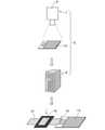
図1は本開示の実施形態の発光表示装置1の輝度補正装置2の構成を示すブロック図であり、図2は輝度補正装置による滅点データの測定および補正データの書き込み手順を示すシーケンス図である。ある。本実施形態の発光表示装置1の輝度補正装置2は、基体としての基板3と、基板3の一方主面3a上に、第1方向Xおよび第1方向Xに垂直に交差する第2方向Yに行列状に位置する複数の画素4と、複数の画素4が映像信号発生部5から出力された入力映像信号を取り込み、取り込まれた入力映像信号に応じた第1輝度B1で発光するように、複数の画素4を制御する制御部6と、を含む。 FIG. 1 is a block diagram showing a configuration of a
複数の自発光型の画素4が行列状に設けられる基体は、基板、透明な板状体、フレキシブルな板状体、曲面を有する基台、段差等の異形面を有する基台等であってよい。基板3は、例えば、透明または不透明なガラス基板、プラスチック基板、セラミック基板等である。基板3の形状は、例えば図2に示すように平面視で矩形板状であるが、矩形状に限らず、台形状、五角形等の多角形状、円形状、楕円形状等の種々の形状であってもよい。 The substrate on which the plurality of self-
複数の画素4は、発光制御部としての画素回路と、一方主面3a上に位置し、所定の画素ピッチでn×m個(nは行数、mは列数であり、それぞれ正の整数である)が行列状に配列され、一方主面3a上にn本のゲート信号線G1~Gn、m本のソース信号線S1~Sm、ゲート信号発生部11、および駆動回路部12を備える。複数の画素4の画素ピッチは、例えば、50μm~500μm程度であってもよく、100μm~400μm程度であってもよく、380μm程度であってもよく、少なくとも300画素/インチの画素密度で配設されていることがよい。各画素4は、電極パッド、および電極パッドに電気的に接続された発光素子、発光素子の輝度、点灯/非点灯等を制御する駆動用薄膜トランジスタ(Thin Film Transistor:TFT)を有している。また、各画素4は、CMOS(Complementary Metal Oxide Semiconductor)トランスファゲート素子、反転論理回路(インバータ)、論理和否定(NOR)回路等を含む画素回路を備えていてもよい。 The plurality of
複数の画素4は、赤色発光用の副画素、緑色発光用の副画素、および青色発光用の副画素のサブピクセルによって構成されてもよい。赤色発光用の副画素は、赤色LED等から成る赤色発光素子を有し、緑色発光用の副画素は、緑色LED等から成る緑色発光素子を有し、青色発光用の副画素は、青色LED等から成る青色発光素子を有している。例えば、これらの副画素は、RGB3色が列方向に並んで1つの画素を構成してもよく、行方向に並んで1つの画素を構成してもよい。 The plurality of
ゲート信号発生部11からn本のゲート信号線G1~Gnを経て供給されるゲート信号(画素選択信号)によって選択状態となった画素4には、駆動回路部12から供給されるソース信号(入力映像信号)がm本のソース信号線S1~Smを経て書き込まれる。駆動用TFTのドレイン電極には、発光素子が接続され、各駆動用TFTのゲート電極にゲート信号がゲート信号線G1~Gn毎に供給されると、ゲート信号が供給された駆動用TFTはオン状態(ソース・ドレイン間が導通状態)となる。オン状態となった駆動用TFTのソース電極に、駆動回路部12から各ソース信号線S1~Smを介してソース信号が供給されると、ソース信号が、駆動用TFTを経てその駆動用TFTのドレイン電極に接続された発光素子に、ドレイン電流として供給される。ソース信号(ドレイン電流)が供給された発光素子は、ソース信号の電位に応じた第1輝度で発光する。このドレイン電流に応じて発光素子の発光強度が制御され、階調が表現される。 The source signal (input) supplied from the
各発光素子は、発光ダイオード(Light Emitting Diode;LED)素子、有機エレクトロルミネセンス(Electroluminescence;EL)素子、および半導体レーザ素子などの自発光型の発光素子である。以下の実施形態では、発光素子として、LED素子を用いた例について説明する。発光素子は、マイクロ発光ダイオード、所謂μLED素子であってもよい。この場合、発光素子は、電極パッドに接続された状態で、一辺の長さが1μm程度以上100μm程度以下、あるいは3μm程度以上10μm程度以下である矩形状の平面視形状を有していてもよい。発光素子は、アノードからカソードに流れる電流の大きさに応じた輝度で発光させることができる。 Each light emitting element is a self-luminous light emitting element such as a light emitting diode (LED) element, an organic electroluminescence (EL) element, and a semiconductor laser element. In the following embodiment, an example in which an LED element is used as the light emitting element will be described. The light emitting element may be a micro light emitting diode, a so-called μLED element. In this case, the light emitting element may have a rectangular planar view shape having a side length of about 1 μm or more and about 100 μm or less, or about 3 μm or more and about 10 μm or less in a state of being connected to the electrode pad. .. The light emitting element can emit light with a brightness corresponding to the magnitude of the current flowing from the anode to the cathode.
制御部6は、複数の画素4のうち、第1輝度B1よりも低い第2輝度B2で発光する滅点画素を検出する滅点検出部7(図2に示す)と、滅点検出部7によって検出された滅点画素の周囲に位置する画素4を補正対象画素として、第2輝度B2よりも高い第3輝度B3で発光させるように補正する輝度補正部8と、を備える。 The
制御部6は、発光表示装置および輝度補正装置の全体の制御及び各種演算を行うコンピュータ装置端末によって実現されてもよい。滅点検出部7は、複数の画素4が設けられた表示パネル13を撮像する撮像装置9を備えていてもよい。撮像装置9は、例えば、CCD(Charge Coupled Devices)カメラ等の半導体撮像方式カメラ、光学式カメラ等によって実現されてもよい。 The
輝度補正部8は、中央演算処理装置(Central Processing Unit;CPU)、プログラムを記憶したROM(Read Only Memory)、RAM(Random Access Memory)、不揮発性メモリ、及び入出力インターフェース(I/O)を含んで構成される。CPU、ROMおよびRAMは、1つのIC(Integrated Circuit)、LSI(Large Scale Integrated Circuit)に格納されていてもよい。これらのCPU、ROM、RAM、不揮発性メモリ、I/Oは、バスラインによって通信可能に接続される。輝度補正処理を行うための制御プログラムは、ROMに予め記憶されている。CPUは、ROMに記憶された制御プログラムを読み出し、RAMから必要なデータを読み出し、あるいは書き込みを行いながら、制御プログラムを実行する。このような制御プログラムを実行することによって、輝度補正部8は輝度補正するための補正データを生成する。このような補正データは、図2に示すように、表示パネル13の入出力部14に接続されたバスライン15上の記憶部16に記憶されており、補助データは、表示パネル13の製造時に付加される。 The
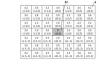
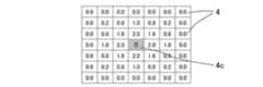
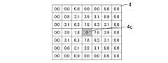
図3は輝度補正装置2の輝度補正処理の手順を示すフローチャートであり、図4は映像信号データパスによる補正データの書き込み手順を示す模式的なシーケンス図である。図5A~図5Dは輝度補正の手順を説明するための複数の画素の模式的平面図である。輝度補正装置2による制御プログラムが実行され、輝度補正処理が開始される。第1工程s1は全画素点灯状態の撮像工程であり、滅点検出部7の撮像装置9によって、全画素4を所定の輝度で点灯状態とした表示パネル13を撮像する。第2工程s2は滅点画素の座標特定工程であり、撮像された画像データから、図5Aに示すように、非点灯画素または点灯しているが目的とする輝度に到達できない低輝度、例えば目的輝度に対して10%以下の輝度の暗点画素を滅点画素4cとして検出し、滅点画素4cの座標(位置)を特定する。滅点画素4cが存在すると、表示パネル13の表示は、例えば、49個(7個×7個)の画素群から成る中間階調の領域の表示が図5Bで示されるように不均一となる。 FIG. 3 is a flowchart showing a procedure of luminance correction processing of the
第3工程s3は補正データの作成工程であり、補正対象画素である周囲画素4aの第3輝度B3が、滅点画素4cに対応する第1輝度B1よりも高い輝度となるように補正する補正データを、輝度補正部8において作成する。なお、滅点画素4cに対応する第1輝度B1とは、入力映像信号によって指定されている階調から決まる本来点灯すべき輝度である。 The third step s3 is a process of creating correction data, and the correction is performed so that the third luminance B3 of the
第3輝度B3は、第1輝度B1に第1輝度B1と第2輝度B2との差分を加えた輝度以上の輝度であってもよい。この場合、滅点画素4cにおいて低下した輝度の分(第1輝度B1と第2輝度B2との差分)以上を、第3輝度B3が補償することができる。その結果、滅点画素4cが視認されることをより抑えることができる。 The third luminance B3 may have a luminance equal to or higher than the luminance obtained by adding the difference between the first luminance B1 and the second luminance B2 to the first luminance B1. In this case, the third luminance B3 can compensate for the reduced brightness (difference between the first luminance B1 and the second luminance B2) in the
また、補正対象画素である周囲画素4aの個数をp個(pは2以上の整数)、第1輝度B1と第2輝度B2との差分をΔBとしたとき、第3輝度B3は、第1輝度B1にΔB/p以上の輝度を加えた輝度であってもよい。この場合、滅点画素4cにおいて低下した輝度の分(第1輝度B1と第2輝度B2との差分ΔB)以上を、複数の第3輝度B3が分担して補償することができる。その結果、滅点画素4cが視認されることをより抑えることができる。 Further, when the number of
補正対象画素である周囲画素4aは、1つの滅点画素4cに対して1個あってもよく、複数あってもよい。図5Cに示すように、補正対象画素である周囲画素4aは複数あり、複数の周囲画素4aは、平面視において滅点画素4cを通る仮想線Lkを中心にして、仮想線Lkの一方の側に位置する周囲画素4aaと、仮想線Lkの他方の側に位置する周囲画素4abと、を含む構成であってもよい。この場合、周囲画素4aaから放射される光および周囲画素4abから放射される光によって、滅点画素4cを効果的に覆うことができる。その結果、滅点画素4cがより視認されにくくなる。仮想線Lkは平面視においてどの方向に向いていてもよい。 The
また、図5Cに示すように、複数の周囲画素4aは、滅点画素4cを中心にして、点対称状の位置にある周囲画素4ab,4acを含む構成であってもよい。この場合、周囲画素4abから放射される光および周囲画素4acから放射される光によって、滅点画素4cをより効果的に覆うことができる。その結果、滅点画素4cがより視認されにくくなる。 Further, as shown in FIG. 5C, the plurality of
また、図5Cに示すように、複数の周囲画素4aは、滅点画素4cの周囲の全周を囲む位置にそれぞれ位置する周囲画素4aを含む構成であってもよい。この場合、滅点画素4cの周囲の全周を囲む周囲画素4aから放射される光によって、滅点画素4cをより効果的に覆うことができる。その結果、滅点画素4cがより視認されにくくなる。 Further, as shown in FIG. 5C, the plurality of
周囲画素4aの第3輝度B3がガウス分布(正規分布)曲線上にある構成であってもよい。この場合、第3輝度B3が滅点輝度4cと周囲画素4aとの距離に対応する。即ち、滅点輝度4cと周囲画素4aとの距離が大きくなるに伴って、第3輝度B3がガウス分布曲線上において小さくなる。これにより、補正による輝度および階調の変化が緩やかになり、視認者にとって違和感が生じにくい画像を提供することができる。第4工程s4は補正データのメモリへの書込み工程であり、輝度補正部8によって算出された、周囲画素4aの座標値および輝度を補正するための補正データは、記憶部16に書き込まれて記憶される。 The third luminance B3 of the
画素ピッチが狭ピッチ化するほど、即ち画素密度が高くなるほど、画素4に冗長回路といった複雑な回路を入れ込めない。一方、狭ピッチ化することにより、人の眼では1画素毎を確認できる分解能以上となる。一般的に人の眼で確認できる画素密度は、300ppi(ピクセル/インチ)程度と言われている。300ppi以上の高画素密度のパネルにおいては、図5Dに示されるように、滅点画素4cがある場合、滅点画素4cに隣接する隣接画素4a1を滅点画素4cの代わりに、滅点画素4c本来の第1輝度B1で点灯させるか、または第1輝度B1よりも高い第3輝度B3で点灯させる。この補正によって、滅点画素4cおよびその周囲画素4aの輝度を平均化し、滅点画素4cを目立たないようにすることができる。 The narrower the pixel pitch, that is, the higher the pixel density, the more complicated circuits such as redundant circuits cannot be inserted into the
図6Aは、各画素4が本来表示すべき輝度値と滅点画素4cの位置とを示す、複数の画素4の模式的平面図である。図6Bは、各画素4に分配された輝度値を示す、複数の画素4の模式的平面図である。図6Cは、周囲の画素4の補正していない輝度値を示す、複数の画素4の模式的平面図である。図6Dは、周囲の画素4の補正後の輝度値を示す、複数の画素4の模式的平面図である。図6Aに示すように、例えば、滅点画素4cが本来点灯すべき第1輝度B1を100に正規化するとともに、滅点画素4cの周囲の画素4の輝度も100とする。図6Bに示すように、滅点画素4cおよびその周囲の25個(5個×5個)の画素4のうち、滅点画素4cを除いた周囲の画素4に、合計が100となるように滅点画素4cが本来点灯すべき輝度100を分配する。図6Cに示すように、周囲の画素4が本来点灯すべき輝度が100であり、従って、補正しない場合の周囲の画素4の輝度はそれぞれ100である。図6Bに示す、周囲の画素4に分配された輝度値と、図6Cに示す、周囲の画素4の補正しない場合の輝度値と、を加算した輝度値を、図6Dに示す。この加算処理は、記憶部16に記憶されている滅点画素4cの座標データに基づき、輝度補正部8に備わったIC、LSI等によって演算が行われる。そして、滅点画素4cの周囲の画素4に、補正された輝度値に対応する駆動信号(ソース信号)を供給する。なお、滅点画素4cの周囲の画素4には、滅点画素4cからの距離が大きいこと等の理由で、補正が不要な画素4があってもよいことは言うまでもない。 FIG. 6A is a schematic plan view of a plurality of
上記の演算(輝度の加算処理)および補正は、1フレーム毎に更新して実施してもよい。また、フレーム周波数が120fps(frames per second)、240fpsと高い場合等には、演算(輝度の加算処理)および補正を、複数フレーム(2フレーム~5フレーム程度)毎に更新して実施してもよい。 The above calculation (luminance addition processing) and correction may be performed by updating every frame. Further, when the frame frequency is as high as 120 fps (frames per second) or 240 fps, the calculation (brightness addition processing) and the correction may be updated every multiple frames (about 2 to 5 frames). good.
図7Aは、滅点画素4cから周囲の画素4までの座標距離を示す、複数の画素4の模式的平面図である。図7Bは、滅点画素4cから周囲の画素4までの座標距離に応じた補正効果を示す、複数の画素4の模式的平面図である。滅点画素4cの周囲の画素4のそれぞれについて、補正対象画素である滅点画素4cの座標(位置)からの距離(座標距離)L(x,y)を算出する。算出した周囲の画素4の座標距離L(x,y)を図7Aに示す。L(x,y)において、xはX方向の座標値、yはY方向の座標値であり、各画素4の位置を表している。 FIG. 7A is a schematic plan view of a plurality of
補正実施距離、即ち滅点画素4cとそれに対して補正を実施する補正対象画素(図5Cに示す周囲画素4a)との最大距離である補正レンジを、Dとする。この補正実施距離Dは、解像度、即ち画素ピッチによって決定する。解像度が低い、即ち画素ピッチが大きい場合にはD=1~2程度の小さな値とし、解像度が高い、即ち画素ピッチが小さい場合にはD=3~4程度の大きな値に設定する。なお、D=1は1画素分の画素レンジ、即ち行方向、列方向および斜め方向において、滅点画素4cから1画素分離隔して隣接する画素間の画素レンジを表す。 Let D be the correction execution distance, that is, the correction range which is the maximum distance between the
一例として、D=3の場合について説明する。まず、座標距離L(x,y)による補正強度係数をL1(x,y)=D-L(x,y)とする。即ち、座標距離L(x,y)が大きくなるに伴って補正効果が小さくなることから、座標距離L(x,y)が大きくなるに伴って補正強度が小さくなるように設定する。このような補正強度係数L1(x,y)の求め方としては、補正強度係数L1(x,y)を定義域とする単調増加関数を用いて分配輝度シフト量を算出する。単調増加関数の関数例1~3について以下に説明する。 As an example, the case of D = 3 will be described. First, the correction intensity coefficient based on the coordinate distance L (x, y) is L1 (x, y) = DL (x, y). That is, since the correction effect decreases as the coordinate distance L (x, y) increases, the correction strength is set to decrease as the coordinate distance L (x, y) increases. As a method of obtaining such a correction intensity coefficient L1 (x, y), the distribution luminance shift amount is calculated using a monotonic increase function having the correction intensity coefficient L1 (x, y) as a domain. The function examples 1 to 3 of the monotonically increasing function will be described below.
(関数例1)
補正強度係数L1(x,y)を、L(x,y)を直接的に用いて算出する場合、補正強度係数L1(x,y)=D-L(x,y)によって算出する。D=3としたときの、滅点画素4cの周囲の各画素4の補正強度係数L1(x,y)を図8Aに示す。この場合の規格化係数S1は式1によって算出される。(Function example 1)
When the correction intensity coefficient L1 (x, y) is calculated by directly using L (x, y), it is calculated by the correction intensity coefficient L1 (x, y) = DL (x, y). FIG. 8A shows the correction intensity coefficient L1 (x, y) of each

例えば、座標(1,0)の画素4について、図7Aおよび図8Aに示すように、L1(1,0)=3-L(1,0)=3-1.0=2.0となる。同様にして、滅点画素4cの周囲を囲む23個の画素4のL1(x,y)を算出する。即ち、座標(-2,2),(-1,2),(0,2),(1,2),(2,2),(-2,1),(-1,1),(0,1),(1,1),(2,1),(-2,0),(-1,0),(2,0),(-2,-1),(-1,-1),(0,-1),(1,-1),(2,-1),(-2,-2),(-1,-2),(0,-2),(1,-2),(2,-2)の画素4のL1(x,y)を算出する(図8Aに示す)。これら24個の画素4のL1(x,y)の合計値S1が、式1に示すように25.6となる。 For example, for
次に、分配輝度シフト量の算出手順について述べる。分配輝度シフト量i(x,y)を下記式2によって算出する。 Next, the procedure for calculating the distributed luminance shift amount will be described. The distributed luminance shift amount i (x, y) is calculated by the

ここで、「分配輝度シフト量」とは、補正対象である画素4(上記の24個の画素4)が本来点灯すべき輝度に、補正によって加算する輝度を表す。式2で表される分配輝度シフト量i(x,y)の合計値であるΣi(x,y)は、I(Iは滅点画素4cの本来の輝度値であり、例えば100とする)となる。例えば、座標(1,0)の画素4のi(x,y)は、(100/25.6)×2.0=7.8となる(図8Bに示す)。ここで、式2においてS1(25.6)を規格化係数とする。同様にして、滅点画素4cの周囲を囲む上記の23個の画素4のi(x,y)を算出する。これら24個の画素4のi(x,y)の合計値Σi(x,y)が100となる。 Here, the "distributed luminance shift amount" represents the luminance added by the correction to the luminance that the
(関数例2)
次に、補正強度係数および分配輝度シフト量i(x,y)を、対数を用いて導出する関数例2について説明する。補正強度係数L2(x,y)を式3によって求める。(Function example 2)
Next, a function example 2 for deriving the correction intensity coefficient and the distributed luminance shift amount i (x, y) using a logarithm will be described. The correction intensity coefficient L2 (x, y) is obtained by

aは補正係数としてのパラメータであり、例えばa=1とする。bは対数関数(log)の底であり、例えば自然対数eとする。滅点画素4cの周囲の24個の画素4について、式3によって算出したL2(x,y)を図9Aに示す。そして、規格化係数S2を次の式4によって算出する。 a is a parameter as a correction coefficient, and for example, a = 1. b is the base of the logarithm function (log), and is, for example, the natural logarithm e. FIG. 9A shows L2 (x, y) calculated by the

次に、上記の24個の画素4について、分配輝度シフト量i(x,y)を次の式5によって算出する。このとき、I=100とする。 Next, for the above 24

算出された各画素4の分配輝度シフト量i(x,y)を、図9Bに示す。 The calculated distribution luminance shift amount i (x, y) of each
(関数例3)
次に、補正強度係数および分配輝度シフト量i(x,y)を、ガウス分布(正規分布)関数を用いて導出する関数例3について説明する。まず、正規分布関数は次の式6によって表される。(Function example 3)
Next, a function example 3 for deriving the correction intensity coefficient and the distributed luminance shift amount i (x, y) using the Gaussian distribution (normal distribution) function will be described. First, the normal distribution function is expressed by the

ここで、σは標準偏差(σ=1)、μは平均値(μ=0.5)であり、規格化係数S3をS3=ΣL3(x,y)=6.0とする。上記の24個の画素4のそれぞれの補正強度係数L3(x,y)を図10Aに示す。 Here, σ is a standard deviation (σ = 1), μ is an average value (μ = 0.5), and the normalization coefficient S3 is S3 = ΣL3 (x, y) = 6.0. The correction intensity coefficient L3 (x, y) of each of the above 24
正規分布を用いた分配輝度シフト量L3(x,y)は、次の式7によって表される。 The distribution luminance shift amount L3 (x, y) using the normal distribution is expressed by the

次に、上記の24個の画素4について、分配輝度シフト量i(x,y)を次の式8によって算出する。 Next, for the above 24

I=100としたときの、上記の24個の画素4のそれぞれの分配輝度シフト量i(x,y)を、図10Bに示す。 FIG. 10B shows the distributed luminance shift amounts i (x, y) of each of the above 24
以上の各実施形態に係る発光表示装置の輝度補正装置は、以下の効果を奏する。μLEDディスプレイ等のような、画素ピッチが狭ピッチでマトリクス状にμLED素子を配置する発光表示装置の場合、例えばマストランスファ実装技術によってμLED素子を基体上に配置し実装することから、配置および実装のミスによって滅点画素が発生しやすく、製造歩留まりを100%まで上げることが困難である。本開示の実施形態に係る輝度補正装置は、滅点画素の視認性を低減するための冗長回路等の複雑な回路を各画素に組み込む必要がなく、その結果画素ピッチを狭ピッチ化することができる。また、滅点画素の周囲の画素を、本来点灯すべき輝度よりも高い輝度で表示させることによって、滅点画素および周囲の画素を含む領域の輝度を、滅点画素が発生していない正常なときの平均輝度とほぼ同一となるように平均化し、その結果滅点画素が視認されにくくなる。滅点画素が人の目で視認可能な画素密度である300画素/インチ程度以上の高密度の画素密度を有する発光表示装置において、滅点画素の視認性を効果的に低減し、高画質の表示を実現することができる。 The luminance correction device of the light emission display device according to each of the above embodiments has the following effects. In the case of a light emitting display device such as a μLED display in which μLED elements are arranged in a matrix with a narrow pixel pitch, the μLED elements are arranged and mounted on a substrate by, for example, mass transfer mounting technology. It is difficult to increase the manufacturing yield to 100% because a blind spot pixel is likely to occur due to a mistake. The luminance correction device according to the embodiment of the present disclosure does not need to incorporate a complicated circuit such as a redundant circuit for reducing the visibility of the blind spot pixel into each pixel, and as a result, the pixel pitch can be narrowed. can. In addition, by displaying the pixels around the blind spot pixels with a brightness higher than the brightness that should be originally lit, the brightness of the area including the blind spot pixels and the surrounding pixels is normal without the blind spot pixels occurring. It is averaged so as to be substantially the same as the average brightness at that time, and as a result, the dead-point pixels are less likely to be visually recognized. In a light emitting display device having a high pixel density of about 300 pixels / inch or more, which is a pixel density at which the blind spot pixels can be visually recognized by the human eye, the visibility of the blind spot pixels is effectively reduced and high image quality is obtained. The display can be realized.
滅点画素の周囲の画素の補正による輝度分布としては、ガウス分布が一例として考えられるが、高密度画素の発光表示装置であれば、滅点画素に隣接する1個以上の隣接画素によって輝度補正を行うこともできる。また、本開示の実施形態に係る輝度補正装置によれば、滅点画素数の多少に拘わらず、滅点画素の視認性を低減することができるので、製品の歩留まりが向上し、製造コストを低減し、高い生産性を実現することができる。 A Gaussian distribution can be considered as an example of the brightness distribution by correcting the pixels around the blind spot pixel, but in the case of a high-density pixel emission display device, the brightness is corrected by one or more adjacent pixels adjacent to the blind spot pixel. Can also be done. Further, according to the brightness correction device according to the embodiment of the present disclosure, the visibility of the blind spot pixels can be reduced regardless of the number of blind spot pixels, so that the yield of the product is improved and the manufacturing cost is reduced. It can be reduced and high productivity can be realized.
以上、本開示の実施形態について詳細に説明したが、また、本開示は上述の実施の形態に限定されるものではなく、本開示の要旨を逸脱しない範囲内において、種々の変更、改良等が可能である。上記各実施形態をそれぞれ構成する全部または一部を、適宜、矛盾しない範囲で組み合わせ可能であることは、言うまでもない。 Although the embodiments of the present disclosure have been described in detail above, the present disclosure is not limited to the above-described embodiments, and various changes, improvements, etc. may be made without departing from the gist of the present disclosure. It is possible. Needless to say, all or part of each of the above embodiments can be combined as appropriate and within a consistent range.
1 発光表示装置
2 輝度補正装置
3 基板
3a 一方主面
4 画素
4c 滅点画素
4a 補正対象画素
5 映像信号発生部
6 制御部
7 滅点検出部
8 輝度補正部
11 ゲート信号発生部
12 駆動回路部
13 表示パネル
16記憶部
G1~Gn ゲート信号線
S1~Sm ソース信号線
X 第1方向
Y 第2方向1
Claims (10)
Translated fromJapanese前記複数の画素が入力映像信号に応じた第1輝度で発光するように、前記複数の画素を制御する制御部を備え、
前記制御部は、
前記複数の画素のうち、前記第1輝度よりも低い第2輝度で発光する滅点画素を検出する滅点検出部と、
前記滅点画素の周囲に位置する画素を補正対象画素として、前記第2輝度よりも高い第3輝度で発光させるように前記補正対象画素の輝度を補正する輝度補正部と、を備えている発光表示装置の輝度補正装置。A luminance correction device for a light emitting display device comprising a substrate and a plurality of self-luminous pixels located in a matrix on the substrate.
A control unit for controlling the plurality of pixels is provided so that the plurality of pixels emit light with the first luminance corresponding to the input video signal.
The control unit
Among the plurality of pixels, a vanishing point detecting unit that detects a vanishing point pixel that emits light at a second luminance lower than the first luminance, and a vanishing point detecting unit.
Light emission including a brightness correction unit that corrects the brightness of the correction target pixel so as to emit light with a third brightness higher than the second brightness, using pixels located around the blind point pixel as the correction target pixel. Luminance correction device for display devices.
複数の前記補正対象画素は、平面視において前記滅点画素を通る仮想線を中心にして、前記仮想線の一方の側に位置する前記補正対象画素と、前記仮想線の他方の側に位置する前記補正対象画素と、を含む請求項1~4のいずれか1項に記載の発光表示装置の輝度補正装置。There are a plurality of the correction target pixels,
The plurality of correction target pixels are located on one side of the virtual line and on the other side of the virtual line with the virtual line passing through the blind point pixel as the center in a plan view. The luminance correction device of the light emission display device according to any one of claims 1 to 4, which includes the correction target pixel.
Priority Applications (1)
| Application Number | Priority Date | Filing Date | Title |
|---|---|---|---|
| JP2020129215AJP2022025979A (en) | 2020-07-30 | 2020-07-30 | Luminance correction device for light emission display device |
Applications Claiming Priority (1)
| Application Number | Priority Date | Filing Date | Title |
|---|---|---|---|
| JP2020129215AJP2022025979A (en) | 2020-07-30 | 2020-07-30 | Luminance correction device for light emission display device |
Publications (1)
| Publication Number | Publication Date |
|---|---|
| JP2022025979Atrue JP2022025979A (en) | 2022-02-10 |
Family
ID=80264859
Family Applications (1)
| Application Number | Title | Priority Date | Filing Date |
|---|---|---|---|
| JP2020129215APendingJP2022025979A (en) | 2020-07-30 | 2020-07-30 | Luminance correction device for light emission display device |
Country Status (1)
| Country | Link |
|---|---|
| JP (1) | JP2022025979A (en) |
Cited By (1)
| Publication number | Priority date | Publication date | Assignee | Title |
|---|---|---|---|---|
| CN116994537A (en)* | 2023-08-09 | 2023-11-03 | 昆山国显光电有限公司 | Compensation method and device for display screen |
Citations (2)
| Publication number | Priority date | Publication date | Assignee | Title |
|---|---|---|---|---|
| JPH0854855A (en)* | 1994-07-13 | 1996-02-27 | Texas Instr Inc <Ti> | Method for reduction of visual influence of flaw existing atinside of spatial light-modulator display and display apparatus |
| KR20150142562A (en)* | 2014-06-11 | 2015-12-22 | 삼성전자주식회사 | Method, apparatus and storage medium for compensating for defect pixel of display |
- 2020
- 2020-07-30JPJP2020129215Apatent/JP2022025979A/enactivePending
Patent Citations (2)
| Publication number | Priority date | Publication date | Assignee | Title |
|---|---|---|---|---|
| JPH0854855A (en)* | 1994-07-13 | 1996-02-27 | Texas Instr Inc <Ti> | Method for reduction of visual influence of flaw existing atinside of spatial light-modulator display and display apparatus |
| KR20150142562A (en)* | 2014-06-11 | 2015-12-22 | 삼성전자주식회사 | Method, apparatus and storage medium for compensating for defect pixel of display |
Cited By (1)
| Publication number | Priority date | Publication date | Assignee | Title |
|---|---|---|---|---|
| CN116994537A (en)* | 2023-08-09 | 2023-11-03 | 昆山国显光电有限公司 | Compensation method and device for display screen |
Similar Documents
| Publication | Publication Date | Title |
|---|---|---|
| US12137594B2 (en) | Display panel and driving method thereof and display apparatus | |
| JP7576938B2 (en) | Display device | |
| US11158246B2 (en) | Display panel, display device, and electronic device | |
| CN104752635B (en) | Method for repairing organic light emitting display | |
| US20180130421A1 (en) | Organic light-emitting diode (oled) display panel, driving method thereof and display apparatus | |
| US10388215B2 (en) | Display device and organic light emitting device | |
| US20060221014A1 (en) | Organic light emitting display and method of driving the same | |
| US20190006429A1 (en) | Electro-optical device and electronic apparatus | |
| JP2012058639A (en) | Organic electroluminescent display device and driving method thereof | |
| EP3026660A1 (en) | Method of performing a multi-time programmable (mtp) operation and organic light-emitting diode (oled) display employing the same | |
| CN110211537B (en) | Display substrate driving method, driving circuit and display device | |
| US20230162641A1 (en) | Display device | |
| JP2022025979A (en) | Luminance correction device for light emission display device | |
| CN113129796B (en) | Display device and rendering method thereof | |
| US10403687B2 (en) | Electro-optical device, method for manufacturing electro-optical device, and electronic apparatus | |
| JP2009282097A (en) | Display and electronic equipment | |
| KR102511047B1 (en) | Organic light emitting display device | |
| US20230135563A1 (en) | Display device for improving displaying quality and display panel thereof | |
| JP7664698B2 (en) | Display device | |
| WO2019058442A1 (en) | Display device and method for driving display device | |
| US20160104420A1 (en) | Organic light emitting diode display | |
| WO2021059783A1 (en) | Display device repair method and display device | |
| US20250148983A1 (en) | Light emitting device, display device, photoelectric conversion device, electronic apparatus, illumination device, and moving body | |
| US12374257B2 (en) | Display device, gamma correction circuit and display driving method | |
| TW202125800A (en) | Display and method for manufacturing display |
Legal Events
| Date | Code | Title | Description |
|---|---|---|---|
| A621 | Written request for application examination | Free format text:JAPANESE INTERMEDIATE CODE: A621 Effective date:20230313 | |
| A977 | Report on retrieval | Free format text:JAPANESE INTERMEDIATE CODE: A971007 Effective date:20231117 | |
| A131 | Notification of reasons for refusal | Free format text:JAPANESE INTERMEDIATE CODE: A131 Effective date:20231205 | |
| A521 | Request for written amendment filed | Free format text:JAPANESE INTERMEDIATE CODE: A523 Effective date:20240202 | |
| A02 | Decision of refusal | Free format text:JAPANESE INTERMEDIATE CODE: A02 Effective date:20240319 |