JP2022023484A - Storage device - Google Patents
Storage deviceDownload PDFInfo
- Publication number
- JP2022023484A JP2022023484AJP2020126450AJP2020126450AJP2022023484AJP 2022023484 AJP2022023484 AJP 2022023484AJP 2020126450 AJP2020126450 AJP 2020126450AJP 2020126450 AJP2020126450 AJP 2020126450AJP 2022023484 AJP2022023484 AJP 2022023484A
- Authority
- JP
- Japan
- Prior art keywords
- voltage
- word line
- line
- memory cell
- select gate
- Prior art date
- Legal status (The legal status is an assumption and is not a legal conclusion. Google has not performed a legal analysis and makes no representation as to the accuracy of the status listed.)
- Pending
Links
Images


Classifications
- G—PHYSICS
- G11—INFORMATION STORAGE
- G11C—STATIC STORES
- G11C13/00—Digital stores characterised by the use of storage elements not covered by groups G11C11/00, G11C23/00, or G11C25/00
- G11C13/0002—Digital stores characterised by the use of storage elements not covered by groups G11C11/00, G11C23/00, or G11C25/00 using resistive RAM [RRAM] elements
- G11C13/0021—Auxiliary circuits
- G11C13/004—Reading or sensing circuits or methods
- G—PHYSICS
- G11—INFORMATION STORAGE
- G11C—STATIC STORES
- G11C13/00—Digital stores characterised by the use of storage elements not covered by groups G11C11/00, G11C23/00, or G11C25/00
- G11C13/0002—Digital stores characterised by the use of storage elements not covered by groups G11C11/00, G11C23/00, or G11C25/00 using resistive RAM [RRAM] elements
- G11C13/0021—Auxiliary circuits
- G11C13/0023—Address circuits or decoders
- G11C13/0028—Word-line or row circuits
- G—PHYSICS
- G11—INFORMATION STORAGE
- G11C—STATIC STORES
- G11C13/00—Digital stores characterised by the use of storage elements not covered by groups G11C11/00, G11C23/00, or G11C25/00
- G11C13/0002—Digital stores characterised by the use of storage elements not covered by groups G11C11/00, G11C23/00, or G11C25/00 using resistive RAM [RRAM] elements
- G11C13/0021—Auxiliary circuits
- G11C13/0023—Address circuits or decoders
- G11C13/0026—Bit-line or column circuits
- G—PHYSICS
- G11—INFORMATION STORAGE
- G11C—STATIC STORES
- G11C13/00—Digital stores characterised by the use of storage elements not covered by groups G11C11/00, G11C23/00, or G11C25/00
- G11C13/0002—Digital stores characterised by the use of storage elements not covered by groups G11C11/00, G11C23/00, or G11C25/00 using resistive RAM [RRAM] elements
- G11C13/0021—Auxiliary circuits
- G11C13/0038—Power supply circuits
- G—PHYSICS
- G11—INFORMATION STORAGE
- G11C—STATIC STORES
- G11C13/00—Digital stores characterised by the use of storage elements not covered by groups G11C11/00, G11C23/00, or G11C25/00
- G11C13/0002—Digital stores characterised by the use of storage elements not covered by groups G11C11/00, G11C23/00, or G11C25/00 using resistive RAM [RRAM] elements
- G11C13/0021—Auxiliary circuits
- G11C13/0069—Writing or programming circuits or methods
- G—PHYSICS
- G11—INFORMATION STORAGE
- G11C—STATIC STORES
- G11C16/00—Erasable programmable read-only memories
- G11C16/02—Erasable programmable read-only memories electrically programmable
- G11C16/04—Erasable programmable read-only memories electrically programmable using variable threshold transistors, e.g. FAMOS
- G11C16/0408—Erasable programmable read-only memories electrically programmable using variable threshold transistors, e.g. FAMOS comprising cells containing floating gate transistors
- G11C16/0433—Erasable programmable read-only memories electrically programmable using variable threshold transistors, e.g. FAMOS comprising cells containing floating gate transistors comprising cells containing a single floating gate transistor and one or more separate select transistors
- G—PHYSICS
- G11—INFORMATION STORAGE
- G11C—STATIC STORES
- G11C16/00—Erasable programmable read-only memories
- G11C16/02—Erasable programmable read-only memories electrically programmable
- G11C16/06—Auxiliary circuits, e.g. for writing into memory
- G11C16/34—Determination of programming status, e.g. threshold voltage, overprogramming or underprogramming, retention
- G11C16/3404—Convergence or correction of memory cell threshold voltages; Repair or recovery of overerased or overprogrammed cells
- G—PHYSICS
- G11—INFORMATION STORAGE
- G11C—STATIC STORES
- G11C13/00—Digital stores characterised by the use of storage elements not covered by groups G11C11/00, G11C23/00, or G11C25/00
- G11C13/0002—Digital stores characterised by the use of storage elements not covered by groups G11C11/00, G11C23/00, or G11C25/00 using resistive RAM [RRAM] elements
- G11C13/0021—Auxiliary circuits
- G11C13/0061—Timing circuits or methods
- G—PHYSICS
- G11—INFORMATION STORAGE
- G11C—STATIC STORES
- G11C2213/00—Indexing scheme relating to G11C13/00 for features not covered by this group
- G11C2213/70—Resistive array aspects
- G11C2213/71—Three dimensional array
- G—PHYSICS
- G11—INFORMATION STORAGE
- G11C—STATIC STORES
- G11C2213/00—Indexing scheme relating to G11C13/00 for features not covered by this group
- G11C2213/70—Resistive array aspects
- G11C2213/75—Array having a NAND structure comprising, for example, memory cells in series or memory elements in series, a memory element being a memory cell in parallel with an access transistor
Landscapes
- Engineering & Computer Science (AREA)
- Microelectronics & Electronic Packaging (AREA)
- Semiconductor Memories (AREA)
Abstract
Description
Translated fromJapanese実施形態は、記憶装置に関する。 The embodiment relates to a storage device.
半導体基板上にReRAM(Resistive Random Access Memory)素子、合金型PCM(Phase Change Memory)素子、iPCM (Interfacial Phase Change Memory)素子、CBRAM(Conduction Bridge RAM)素子等の抵抗変化型記憶素子が集積化された記憶装置(半導体集積回路装置)が提案されている。 Resistance change memory elements such as ReRAM (Resistive Random Access Memory) elements, alloy type PCM (Phase Change Memory) elements, iPCM (Interfacial Phase Change Memory) elements, and CBRAM (Conduction Bridge RAM) elements are integrated on a semiconductor substrate. A storage device (semiconductor integrated circuit device) has been proposed.
上述したような抵抗変化型記憶素子を用いた記憶装置において、製造が容易で、開発期間を短縮出来、プロセスコストを軽減出来る様な高集積化が可能となる3次元構造が提案されて来なかった。 In the storage device using the resistance change type storage element as described above, a three-dimensional structure that is easy to manufacture, can shorten the development period, and can be highly integrated so as to reduce the process cost has not been proposed. rice field.
信頼性を向上できる3次元構造の記憶装置を提案する。 We propose a storage device with a three-dimensional structure that can improve reliability.
実施形態に係る記憶装置は、半導体基板に直交する第1方向に延伸する抵抗変化記憶領域と、第1方向に延伸し、抵抗変化記憶領域に接する半導体層と、第1方向に延伸し、半導体層に接する絶縁体層と、第1方向に直行する第2方向に延伸し、絶縁体層に接する第1ワード線と、第2方向に延伸し、絶縁体層に接し、第1方向において第1ワード線と異なる位置に位置する第2ワード線と、第2方向に延伸し、絶縁体層に接する第1セレクトゲート線と、第1方向及び第2方向に直行する第3方向に延伸し、半導体層に接するビット線と、を含む。第2方向及び第3方向からなる第1平面において、抵抗変化記憶領域、半導体層、及び絶縁体層と、第1ワード線または第2ワード線とが交差する部分がメモリセルとして機能する。第1平面において、半導体層、及び絶縁体層と、第1セレクトゲート線とが交差する部分が第1選択トランジスタとして機能する。第1ワード線に対応するメモリセルに記憶された情報を読み出す場合、またはメモリセルに情報を記憶する場合、第1セレクトゲート線の電圧は第1電圧とされ、且つ第1ワード線及び第2ワード線の電圧は第1電圧よりも高い第2電圧とされた後、第1セレクトゲート線の電圧は第1電圧から、第2電圧よりも高い第3電圧に立ち上げられ、少なくとも第1セレクトゲート線の電圧が第2電圧まで上げられた後、第1ワード線の電圧は第2電圧から第1電圧に立ち下げられ、第2ワード線の電圧は第2電圧から第4電圧に立ち上げられる。 The storage device according to the embodiment has a resistance change storage region extending in the first direction orthogonal to the semiconductor substrate, a semiconductor layer extending in the first direction and in contact with the resistance change storage region, and a semiconductor extending in the first direction. The insulator layer in contact with the layer, the first word wire extending in the second direction orthogonal to the first direction and in contact with the insulator layer, and the first word wire extending in the second direction and in contact with the insulator layer, and the first in the first direction. A second word wire located at a position different from the first word wire, a first select gate wire extending in the second direction and in contact with the insulator layer, and a third direction orthogonal to the first and second directions. , A bit wire in contact with the semiconductor layer, and the like. In the first plane composed of the second direction and the third direction, the portion where the resistance change storage area, the semiconductor layer, and the insulator layer intersect with the first word line or the second word line functions as a memory cell. In the first plane, the portion where the semiconductor layer and the insulator layer intersect with the first select gate line functions as the first selection transistor. When reading the information stored in the memory cell corresponding to the first word line, or when storing the information in the memory cell, the voltage of the first select gate line is set to the first voltage, and the first word line and the second. After the voltage of the ward line is set to the second voltage higher than the first voltage, the voltage of the first select gate line is raised from the first voltage to the third voltage higher than the second voltage, and at least the first select. After the voltage of the gate line is raised to the second voltage, the voltage of the first word line is lowered from the second voltage to the first voltage, and the voltage of the second word line is raised from the second voltage to the fourth voltage. Be done.
以下、図面を参照して実施形態について説明する。なお、以下の説明において、同一の機能及び構成を有する構成要素については、共通する参照符号を付す。 Hereinafter, embodiments will be described with reference to the drawings. In the following description, components having the same function and configuration are designated by a common reference numeral.
<1>第1実施形態
第1実施形態に係る記憶装置について説明する。<1> First embodiment
The storage device according to the first embodiment will be described.
<1-1>構成
<1-1-1>メモリシステムの全体構成
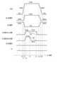
まず、本実施形態に係る記憶装置(以下、「メモリチップ」とも表記する)を備えるメモリシステムの大まかな全体構成について、図1を用いて説明する。<1-1> Configuration <1-1-1> Overall configuration of the memory system
First, a rough overall configuration of a memory system including a storage device (hereinafter, also referred to as a “memory chip”) according to the present embodiment will be described with reference to FIG.
図1に示すようにメモリシステム1は、メモリチップ100とコントローラ200とを備えている。メモリチップ100とコントローラ200とは、例えばそれらの組み合わせにより一つの半導体装置を構成しても良く、その例としてはSDTMカードのようなメモリカードや、SSD(solid state drive)等が挙げられる。As shown in FIG. 1, the
メモリチップ100は複数のメモリセルを備え、データを不揮発に記憶する。コントローラ200は、メモリバスによってメモリチップ100に接続され、ホストバスによってホスト300に接続される。そしてコントローラ200は、メモリチップ100を制御し、またホスト300から受信したホストコマンドに応答して、メモリチップ100にアクセスする。ホスト300は、例えばデジタルカメラやパーソナルコンピュータ等であり、ホストバスは、例えばSDTMインターフェースに従ったバスである。メモリバスは、メモリインターフェースに従った信号の送受信を行う。The
<1-1-2>コントローラ200の構成
引き続き図1を用いて、コントローラ200の構成の詳細について説明する。<1-1-2> Configuration of
Subsequently, the details of the configuration of the
図1に示すようにコントローラ200は、ホストインターフェース回路(ホストI/F)210、内蔵メモリ(RAM:Random Access Memory)220、プロセッサ(CPU:Central Processing Unit)230、バッファメモリ240、メモリインターフェース回路(メモリI/F)250、及びECC(Error Checking and Correcting)回路260を備えている。 As shown in FIG. 1, the
ホストインターフェース回路210は、ホストバスを介してホスト300と接続され、ホスト300から受信したホストコマンド及びデータを、それぞれプロセッサ230及びバッファメモリ240に転送する。またホストインターフェース回路210は、プロセッサ230の命令に応答して、バッファメモリ240内のデータをホスト300へ転送する。 The
プロセッサ230は、コントローラ200全体の動作を制御する。例えばプロセッサ230は、ホスト300から読み出しに関するホストコマンドを受信した際には、それに応答して、メモリインターフェース回路250にメモリチップ100へ読み出しコマンド(メモリコマンド)を発行させる。プロセッサ230は、ホスト300から書き込みに関するホストコマンドを受信した際も、同様の動作を行う。またプロセッサ230は、メモリチップ100を管理するための様々な処理(ウェアレベリング等)を実行する。 The
メモリインターフェース回路250は、メモリバスを介してメモリチップ100と接続され、メモリチップ100との通信を司る。そしてメモリインターフェース回路250は、プロセッサ230から受信した命令に基づき、種々の信号をメモリチップ100へ送信し、またメモリチップ100から種々の信号を受信する。 The
バッファメモリ240は、メモリチップ100への書き込みデータやメモリチップ100からの読み出しデータを一時的に保持する。 The
内蔵メモリ220は、例えばDRAMやSRAM等の半導体メモリであり、プロセッサ230の作業領域として使用される。そして内蔵メモリ220は、メモリチップ100を管理するためのファームウェアや、後述するシフトテーブル、履歴テーブル、フラグテーブル等の、各種の管理テーブル等を保持する。 The built-in
ECC回路260は、メモリチップ100に記憶されるデータに関する誤り検出及び誤り訂正処理を行う。すなわちECC回路260は、データの書き込み時には誤り訂正符号を生成して、これを書き込みデータに付与し、データの読み出し時にはこれを復号する。 The
<1-1-3>メモリチップ100の構成
次に、メモリチップ100の構成について説明する。<1-1-3> Configuration of
Next, the configuration of the
図1に示すようにメモリチップ100は、メモリセルアレイ110、ロウデコーダ120、ドライバ回路130、センスアンプ140、アドレスレジスタ150、コマンドレジスタ160、及びシーケンサ170を備える。 As shown in FIG. 1, the
メモリセルアレイ110は、ロウ(ワード線)及びカラム(ビット線)に対応付けられた複数の不揮発性のメモリセルを含む複数のブロックBLKを備えている。図1では一例として4つのブロックBLK0~BLK3が図示されている。そしてメモリセルアレイ110は、コントローラ200から与えられたデータを記憶する。 The
ロウデコーダ120は、アドレスレジスタ150内のブロックアドレスBAに基づいてブロックBLK0~BLK3のいずれかを選択し、更に選択したブロックBLKにおけるワード線方向を選択する。 The
ドライバ回路130は、アドレスレジスタ150内のページアドレスPAに基づいて、選択されたブロックBLKに対して、ロウデコーダ120を介して電圧を供給する。ドライバ回路130は、例えばソース線ドライバ等も含む。 The
センスアンプ140は、ビット線BL毎に設けられるセンスアンプモジュールを備え、データの読み出し時には、メモリセルアレイ110から読み出されたデータをセンスし、必要な演算を行う。そして、このデータDATをコントローラ200に出力する。データの書き込み時には、コントローラ200から受信した書き込みデータDATを、メモリセルアレイ110に転送する。 The sense amplifier 140 includes a sense amplifier module provided for each bit line BL, and when reading data, it senses the data read from the
アドレスレジスタ150は、コントローラ200から受信したアドレスADDを保持する。このアドレスADDには、前述のブロックアドレスBAとページアドレスPAとが含まれる。コマンドレジスタ160は、コントローラ200から受信したコマンドCMDを保持する。 The address register 150 holds the address ADD received from the
シーケンサ170は、コマンドレジスタ160に保持されたコマンドCMDに基づき、メモリチップ100全体の動作を制御する。 The sequencer 170 controls the operation of the
<1-1-4>メモリセルアレイ110の回路構成
次に、メモリセルアレイ110の回路(等価回路)構成について図2を用いて説明する。<1-1-4> Circuit configuration of
Next, the circuit (equivalent circuit) configuration of the
図2に示すように、メモリセルアレイ110のブロックBLKは例えば4つのストリングユニットSU(SU(0)~SU(3))を含む。なお、ブロックBLK内のストリングユニットSUの個数は任意である。また各々のストリングユニットSUは、複数のメモリセルストリングMSを含む。 As shown in FIG. 2, the block BLK of the
メモリセルストリングMSの各々は、例えば16個のメモリセルMC(MC(0)~MC(15))、及び選択トランジスタST(1)を含んでいる。以下、メモリセルMC(0)~MC(15)のそれぞれを限定しない場合は、メモリセルMCと表記する。更に、メモリセルストリングMSの各々に含まれる選択トランジスタST(1)の個数は任意であり、少なくとも1個以上あればよい。 Each of the memory cell string MSs includes, for example, 16 memory cells MC (MC (0) to MC (15)) and a selection transistor ST (1). Hereinafter, when each of the memory cells MC (0) to MC (15) is not limited, it is referred to as a memory cell MC. Further, the number of the selection transistors ST (1) included in each of the memory cell string MS is arbitrary, and may be at least one.
メモリセルMCは、記憶素子(抵抗変化記憶領域/抵抗変化層/抵抗変化素子)MR、及びセレクタSWを含む。記憶素子MRの一例としては、合金型相転移素子(Ge2Sb2Te5)が挙げられる。本実施形態の記憶素子MRは、結晶状態が変化することにより、低抵抗または高抵抗の状態になる。以下では、記憶素子MRの結晶状態が変化することを「相変化」と呼び、記憶素子MRが低抵抗状態(LRS)にある場合を「セット状態」と記載、高抵抗状態(HRS)にある場合を「リセット状態」と記載する。また、本実施形態でのセレクタSWは、半導体層、ゲート絶縁膜、及びゲート電極を含んでいる。メモリセルMCにおいて、記憶素子MR、及びセレクタSWは並列に接続されている。また、メモリセルストリングMSの各々に含まれるメモリセルMCの個数は、8個、32個、48個、64個、96個、または128個等であってもよく、その数は限定されるものではない。The memory cell MC includes a storage element (resistance change storage area / resistance change layer / resistance change element) MR and a selector SW. As an example of the storage element MR, an alloy type phase transition element (Ge2 Sb2 Te5 ) can be mentioned. The storage element MR of the present embodiment becomes a state of low resistance or high resistance by changing the crystal state. In the following, the change in the crystal state of the storage element MR is referred to as "phase change", and the case where the storage element MR is in the low resistance state (LRS) is described as the "set state", and is in the high resistance state (HRS). The case is described as "reset state". Further, the selector SW in the present embodiment includes a semiconductor layer, a gate insulating film, and a gate electrode. In the memory cell MC, the storage element MR and the selector SW are connected in parallel. Further, the number of memory cells MC included in each of the memory cell string MSs may be 8, 32, 48, 64, 96, 128, or the like, and the number thereof is limited. is not it.
メモリセルMCが非選択である場合は、セレクタSWをオン状態(導通状態)にする。図3に示すように、セレクタSWがオン状態である場合、セレクタSWの半導体層に反転層(チャネル層)が出来るため、電流は反転層を流れる。なお、記憶素子MRの低抵抗状態における抵抗値は、セレクタSWのオン状態における半導体層の抵抗値よりも10倍(一桁)以上高い。そのため、並列に接続された記憶素子MRには電流が流れない。ところで、メモリセルMCにデータを記憶するのは、記憶素子MRである。そのため、記憶素子MRに電流が流れないということは、メモリセルMCは選択されない事を意味する。 When the memory cell MC is not selected, the selector SW is turned on (conducting state). As shown in FIG. 3, when the selector SW is in the ON state, an inversion layer (channel layer) is formed in the semiconductor layer of the selector SW, so that the current flows through the inversion layer. The resistance value of the storage element MR in the low resistance state is 10 times (one digit) or more higher than the resistance value of the semiconductor layer in the on state of the selector SW. Therefore, no current flows through the storage elements MR connected in parallel. By the way, it is the storage element MR that stores the data in the memory cell MC. Therefore, the fact that no current flows through the storage element MR means that the memory cell MC is not selected.
また、メモリセルMCが選択である場合は、セレクタSWをオフ状態(非導通状態)にする。図4に示すように、セレクタSWがオフ状態である場合、セレクタSWの半導体層に反転層(チャネル層)が出来ない。また、記憶素子MRの高抵抗状態における抵抗値は、セレクタSWのオフ状態における半導体層の抵抗値よりも10倍(一桁)以上低い。そのため、電流は半導体層を流れず、並列に接続された記憶素子MRを流れる。記憶素子MRに電流が流れるということは、メモリセルMCが選択される事を意味する。 When the memory cell MC is selected, the selector SW is turned off (non-conducting state). As shown in FIG. 4, when the selector SW is in the off state, an inversion layer (channel layer) cannot be formed on the semiconductor layer of the selector SW. Further, the resistance value of the storage element MR in the high resistance state is 10 times (one digit) or more lower than the resistance value of the semiconductor layer in the off state of the selector SW. Therefore, the current does not flow through the semiconductor layer, but flows through the storage element MR connected in parallel. The fact that a current flows through the memory element MR means that the memory cell MC is selected.
図2に戻って、メモリセルアレイ110の説明を続ける。各メモリセルストリングMSに含まれたメモリセルMC(0)~MC(15)は、選択トランジスタST(1)とソース線SLとの間に直列接続されている。同一のブロックBLKに含まれた各メモリセルストリングMSのメモリセルMC(0)の制御ゲート(複数の制御ゲート)は、ワード線WL(0)に共通に接続されている。同様に、同一のブロックBLKに含まれた複数のメモリセルストリングMSのメモリセルMC(1)~MC(15)の制御ゲートは、それぞれワード線WL(1)~WL(15)に共通に接続されている。 Returning to FIG. 2, the description of the
以下、ワード線WL(0)~(15)のそれぞれを限定しない場合は、ワード線WLと表記する。 Hereinafter, when each of the word lines WL (0) to (15) is not limited, it is referred to as a word line WL.
尚、以下の説明では、それぞれのストリングユニットSU内で共通のワード線WLに接続された複数のメモリセルMCをページと称する。 In the following description, a plurality of memory cell MCs connected to a common word line WL in each string unit SU will be referred to as a page.
ストリングユニットSU内の複数の選択トランジスタST(1)のゲートはセレクトゲート線SGDに共通に接続される。より具体的には、ストリングユニットSU(0)内の複数の選択トランジスタST(1)のゲートはセレクトゲート線SGD(0)に共通に接続される。同様に、ストリングユニットSU(1)内の複数の選択トランジスタST(1)のゲートはセレクトゲート線SGD(1)に共通に接続される。ストリングユニットSU(2)及びSU(3)においても同様である。 The gates of the plurality of selection transistors ST (1) in the string unit SU are commonly connected to the select gate line SGD. More specifically, the gates of the plurality of selection transistors ST (1) in the string unit SU (0) are commonly connected to the select gate line SGD (0). Similarly, the gates of the plurality of selection transistors ST (1) in the string unit SU (1) are commonly connected to the select gate line SGD (1). The same applies to the string units SU (2) and SU (3).
以下、セレクトゲート線SGD(SGD(0)、SGD(1)、…)のそれぞれを限定しない場合は、セレクトゲート線SGDと表記する。 Hereinafter, when each of the select gate line SGD (SGD (0), SGD (1), ...) Is not limited, it is referred to as the select gate line SGD.
セレクトゲート線SGD、並びにワード線WLの各々は、ロウデコーダ120によって独立に制御される。 Each of the select gate line SGD and the word line WL is independently controlled by the
また、メモリセルアレイ110内において同一列にあるメモリセルストリングMSの選択トランジスタST(1)のドレインは、ビット線BL(BL(0)~BL(m)、但しmは1以上の自然数)に共通接続される。すなわちビット線BLは、複数のブロックBLK間でメモリセルストリングMSを共通に接続する。更に、複数のメモリセルMC(15)のソースは、ソース線SLに共通に接続されている。 Further, the drain of the selection transistor ST (1) of the memory cell string MS in the same row in the
つまりストリングユニットSUは、異なるビット線BLに接続され、且つ同一のセレクトゲート線SGDに接続されたメモリセルストリングMSを複数含む。またブロックBLKは、ワード線WLを共通にする複数のストリングユニットSUを複数含む。そしてメモリセルアレイ110は、ビット線BLを共通にする複数のブロックBLKを複数含む。 That is, the string unit SU includes a plurality of memory cell string MSs connected to different bit lines BL and connected to the same select gate line SGD. Further, the block BLK includes a plurality of string units SU having a common word line WL. The
<1-1-5>メモリセルアレイ110の構造
以下に、第1実施形態におけるメモリセルアレイ110の構造の一例について説明する。尚、以下で参照される図面において、X方向はビット線BLの延伸方向に対応し、Y方向はワード線WLの延伸方向に対応し、Z方向はメモリセルアレイ110が形成される半導体基板20の表面に対する鉛直(垂直)方向に対応している。なお、以下、各図では、図を見易くするために絶縁体層(層間絶縁膜)、配線、コンタクト等の構成要素が適宜省略されている。<1-1-5> Structure of the
図5は、第1実施形態に係るメモリチップ100の備えるメモリセルアレイ110の断面構造の一例を示している。図5に示すように、メモリセルアレイ110は、例えば導電体層21~24を含んでいる。導電体層21~25は、半導体基板20の上方に設けられる。 FIG. 5 shows an example of the cross-sectional structure of the
具体的には、半導体基板20のZ方向における上方に、絶縁体層を介して導電体層(電位印加電極、電圧印加電極)21が設けられる。例えば半導体基板20と導電体層21との間の絶縁体層には、センスアンプ140等の回路が設けられてもよい。導電体層21は、例えばXY平面に沿って広がった板状に形成され、ソース線SLとして使用される。導電体層21は、例えばシリコン(Si)を含んでいる。 Specifically, a conductor layer (potential application electrode, voltage application electrode) 21 is provided above the
導電体層21のZ方向における上方に、絶縁体層と導電体層(電位印加電極、電圧印加電極)22とが交互に積層される。導電体層22は、例えばXY平面に沿って広がった板状に形成される。例えば、積層された複数の導電体層22は、半導体基板20側から順に、それぞれワード線WL(15)~WL(0)として使用される。導電体層22は、例えばタングステン(W)を含んでいる。 The insulator layer and the conductor layer (potential application electrode, voltage application electrode) 22 are alternately laminated above the
Z方向における最上層の導電体層22(WL(0))の上方に、絶縁体層を介して例えば導電体層(電位印加電極、電圧印加電極)23が積層される。導電体層23は、Y方向に延伸し、X方向において、後述するセレクトピラーSPごとに分断されている。分断された導電体層23は、それぞれセレクトゲート線SGD(0)~(3)として使用される。導電体層23は、例えばタングステン(W)を含んでいる。 For example, a conductor layer (potential application electrode, voltage application electrode) 23 is laminated on the uppermost conductor layer 22 (WL (0)) in the Z direction via an insulator layer. The
導電体層23のZ方向における上方に、導電体層(電位印加電極、電圧印加電極)24が設けられる。例えば導電体層24は、X方向に沿って延伸したライン状に形成され、ビット線BLとして使用される。導電体層24は、例えば銅(Cu)を含んでいる。 A conductor layer (potential application electrode, voltage application electrode) 24 is provided above the
メモリピラーMPは、Z方向に沿って延伸する円柱形状であり、導電体層22を貫通し、底部が導電体層21に達している。また、メモリピラーMPは、例えばコア部材30、抵抗変化層31、半導体層32、及び絶縁体層33を含んでいる。具体的には、導電体層22及び絶縁体層の積層構造を貫通し、底部が導電体層21に達するメモリホールMHが設けられる。メモリホールMHは、例えばZ方向に延伸する円筒形状である。メモリホールMHの内部(内壁)に絶縁体層33、半導体層32、抵抗変化層31、コア部材30、が順に設けられることにより、メモリピラーMPが構成される。具体的には、メモリピラーMPは、メモリホールMHの内壁を覆い、Z方向に延伸する円筒形状の絶縁体層33、絶縁体層33の内壁を覆い、Z方向に延伸する円筒形状の半導体層32、並びに半導体層32の内壁を覆い、Z方向に延伸する円筒形状または円柱形状の抵抗変化記憶領域31を備える。 The memory pillar MP has a cylindrical shape extending in the Z direction, penetrates the
メモリピラーMP上には、導電体層23を貫通する円柱形状のセレクトピラーSPが設けられる。また、セレクトピラーSPは、例えば半導体層32、及び絶縁体層33を含んでいる。具体的には、セレクトピラーSPは、導電体層23を貫通し、底部がメモリピラーMPに達するSGDホールSHが設けられ、SGDホールSHの内部に絶縁体層33、半導体層32が順に設けられる。 A cylindrical select pillar SP penetrating the
なお、メモリホールMHとSGDホールSHとの境界を含む層は、最上層の導電体層22と導電体層23との間の層に含まれている。 The layer including the boundary between the memory hole MH and the SGD hole SH is included in the layer between the
コア部材30は、例えば窒化シリコン(SiN)等の絶縁体を含んでいる。コア部材30は、例えばZ方向に延伸する円柱形状である。 The
抵抗変化層31は、コア部材30の側面(外周)を覆っている(コア部材30に接している)。抵抗変化層31は、例えばZ方向に延伸し、円筒形状に設けられる。例えば、抵抗変化層31の底部は、導電体層21に接触している。 The
メモリピラーMPにおける半導体層32は、抵抗変化層31の側面(外周)を覆っている(抵抗変化層31に接している)。メモリピラーMPにおける半導体層32は、例えばZ方向に延伸し、円筒形状に設けられる。例えば、半導体層32の底部は、導電体層21に接触している。 The
セレクトピラーSPにおける半導体層32は、例えば円柱形状である。セレクトピラーSPの半導体層32の底辺は、メモリピラーMPの半導体層32、抵抗変化層31、コア部材30に接触している。 The
絶縁体層33は、半導体層32の側面を覆っている。絶縁体層33は、例えば円筒形状に設けられた部分を含んでいる。絶縁体層33は、例えば酸化シリコン(SiO2)等の絶縁体を含んでいる。The
また、導電体層22は、メモリピラーMPにおける絶縁体層33の側面の一部を覆う(絶縁体層33に接する)。 Further, the
また、導電体層23は、セレクトピラーSPにおける絶縁体層33の側面の一部を覆う(絶縁体層33に接する)。 Further, the
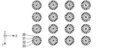
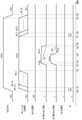
次に、図6を用いて、導電体層23の平面図について説明する。図6は、図5のA-A線に沿った平面図である。 Next, a plan view of the
図6に示すように、導電体層23を貫通するSGDホールSH内に、絶縁体層33と、半導体層32と、が設けられている。そして、導電体層23は、選択トランジスタST(1)のセレクトゲート線SGD(0)~SGD(3)として機能し、絶縁体層33は、選択トランジスタST(1)のゲート絶縁膜として機能し、半導体層32は、選択トランジスタST(1)の半導体層として機能する。この選択トランジスタST(1)を用いることで、1本のワード線WL毎にメモリピラーMPを選択することができる。選択トランジスタST(1)をオン状態にすることで、メモリピラーMPの抵抗変化層31に接する半導体層32に反転層が形成され、反転層を介して電流を流す事により、メモリピラーMPを選択することができる。 As shown in FIG. 6, an
次に、図7を用いて、Z方向におけるメモリセルMC間の平面図について説明する。図7は、図5のB-B線に沿った平面図である。図7に示すコア部材30、抵抗変化層31、半導体層32、及び絶縁体層33は、Z方向におけるメモリセルMC間に相当し、電流は半導体層32の中を流れる。 Next, a plan view between the memory cells MC in the Z direction will be described with reference to FIG. 7. FIG. 7 is a plan view taken along the line BB of FIG. The
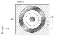
次に、図8及び図9を用いて、導電体層22の平面図について説明する。図8は、図5のC-C線に沿った平面図である。図9は、一つのメモリセルMCを抽出した平面図である。 Next, a plan view of the
図9に示すように、メモリセルMCは、板状のワード線WLと、メモリピラーMPの交点に設けられる。具体的には図9に示すように、導電体層22を貫通するメモリホールMH内に、絶縁体層33と、半導体層32、抵抗変化層31、コア部材30と、が設けられている。そして、導電体層22は、メモリセルMCのセレクタSWのワード線WLとして機能し、絶縁体層33は、メモリセルMCのセレクタSWのゲート絶縁膜として機能し、半導体層32は、メモリセルMCのセレクタSWの半導体層として機能する。抵抗変化層31は、メモリセルMCの記憶素子MRとして機能する。 As shown in FIG. 9, the memory cell MC is provided at the intersection of the plate-shaped word line WL and the memory pillar MP. Specifically, as shown in FIG. 9, an
次に、図10を用いて、導電体層21の平面図について説明する。図10は、図5のD-D線に沿った平面図である。 Next, a plan view of the
導電体層21は、板状であり、ビット線BLから電流を流し込むために、一定の低電位に設定される。図10に示すように導電体層21(ソース線SL)は、導電体層22(ワード線WL)と同様に板状である。 The
次に、図11を用いて、メモリセルアレイ110の断面構造の一例について説明する。図11は、図5のE-E線に沿った断面図である。図11は、図5と直交する方向の断面である。図5及び図11を併せて参照すると、メモリピラーMPは、コア部材30を中心に同心円状の形状をしている事が分かる。 Next, an example of the cross-sectional structure of the
<1-2>動作
<1-2-1>概要
続いて、本実施形態に係るメモリチップ100の動作の概要について説明する。<1-2> Operation <1-2-1> Outline Next, an outline of the operation of the
本実施形態に係るメモリチップ100において、読み出し動作及び書き込み動作は、ビット線BLと、ソース線SLと、の間に電流を流すことによって行う。 In the
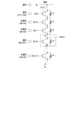
図12及び図13を用いて、読み出し動作または書き込み動作を行うメモリセルMCを選択する方法について概略的に説明する。図12は、一つのメモリセルストリングMSを抜き出した回路図である。図13は、一つのメモリセルストリングMSに対応するメモリピラーMPを抜き出した断面図である。 A method of selecting a memory cell MC to perform a read operation or a write operation will be schematically described with reference to FIGS. 12 and 13. FIG. 12 is a circuit diagram obtained by extracting one memory cell string MS. FIG. 13 is a cross-sectional view of a memory pillar MP corresponding to one memory cell string MS.
図12及び図13に示すように、選択したいメモリセルMC(例えばMC(2))が属するメモリピラーMPに接する選択トランジスタST(1)のセレクトゲート線SGDに所定の電圧(正の電圧)を印加する。これにより、選択トランジスタST(1)の半導体層32に反転層が形成され、電流が流れることができる状態となる(オン状態)。これにより、ビット線BLと、選択トランジスタST(1)と、選択トランジスタST(1)に接するメモリピラーMPの半導体層32が導通される。更に、選択メモリセルMC(2)に対応するワード線WL(2)には、例えば0[V]または電圧VSSを印加し、非選択メモリセルMCに対応するワード線WL(0)、(1)、(3)~(15)には所定の電圧(正の電圧)を印加する。これにより、ビット線BLとソース線SLと間を流れる電流パスは、選択したいメモリセルMC(2)においては、記憶素子MRを流れ、非選択のメモリセルMC(0)、(1)、(3)~(15)においては、セレクタSWの半導体層32を流れる。図13に示すように、メモリピラーMPの中心部分には絶縁体層であるコア部材30が設けられているので、選択メモリセルMCにおいて電流は、コア部材30を取り囲む抵抗変化層31を流れる。抵抗変化層31の材質の一例としては合金型相転移素子(Ge2Sb2Te5)が挙げられる。As shown in FIGS. 12 and 13, a predetermined voltage (positive voltage) is applied to the select gate line SGD of the selection transistor ST (1) in contact with the memory pillar MP to which the memory cell MC (for example, MC (2)) to be selected belongs. Apply. As a result, an inversion layer is formed on the
このようにする事で、読み出し動作時、書き込み動作時、共に抵抗変化層31を選択出来る様にする。本方式を3次元NAND型フラッシュメモリと比較した場合、より低電圧、且つより高速で動作出来る様になる他、書き換え回数の制約も少なく、書き込み時間も短くて済む利点がある。 By doing so, the
なお、本実施形態では、3次元NAND型フラッシュメモリと異なる抵抗変化型メモリであり、動作において消去動作が存在しない。 In this embodiment, the resistance change type memory is different from the three-dimensional NAND type flash memory, and there is no erasing operation in the operation.
また、書き込み動作、または読み出し動作は選択トランジスタST(1)をオン状態にして、ビット線BLと、ソース線SLと、の間に電流を流して行う。そのため、全メモリセルストリングMSを選択する必要は無く、1本のセレクトゲート線に接続される任意のビット線BL単位(カラム単位)で選択を行う事が出来る。 Further, the write operation or the read operation is performed by turning on the selection transistor ST (1) and passing a current between the bit line BL and the source line SL. Therefore, it is not necessary to select all memory cell string MSs, and selection can be made in any bit line BL unit (column unit) connected to one select gate line.
書き込み動作、または読み出し動作を行いたくないメモリセルストリングMSに対しては、ソース線SLの電圧=ビット線BLの電圧に設定しておけば、書き込み動作、または読み出し動作が行われる事は無い。 For the memory cell string MS that does not want to perform the write operation or the read operation, if the voltage of the source line SL = the voltage of the bit line BL is set, the write operation or the read operation is not performed.
また、3次元NAND型フラッシュメモリのように、ブロックBLK単位で消去動作を行う必要もなく、選択トランジスタST(1)単位でセット/リセットの書き込み動作が出来る。 Further, unlike the three-dimensional NAND flash memory, it is not necessary to perform the erase operation in the block BLK unit, and the set / reset write operation can be performed in the selection transistor ST (1) unit.
ワード線WLは積層方向(Z方向)で任意のメモリセルMCを選択するように機能する。同一XY平面における複数のメモリセルMCのゲート電極に、共通のワード線WLが接続されてよい。また、複数のメモリセルストリングMSに共通のソース線SLが接続されてよい。特にビット線BL延伸方向(X方向)に隣接する複数の前記メモリセルストリングMSにおいて、各ワード線WLおよびソース線SLは、共有化されてよい。 The word line WL functions to select an arbitrary memory cell MC in the stacking direction (Z direction). A common word line WL may be connected to the gate electrodes of a plurality of memory cells MC in the same XY plane. Further, a source line SL common to a plurality of memory cell string MSs may be connected. In particular, in the plurality of memory cell string MSs adjacent to the bit line BL extending direction (X direction), each word line WL and a source line SL may be shared.
例えば、ワード線WLと、ソース線SLはビット線BL延伸方向(X方向)とワード線WL延伸方向(Y方向)に延びた板状の形状をしている場合を考える。メモリセルMCの選択は選択トランジスタST(1)をオン状態にした上に、ビット線BLからソース線SLに電流を流さなければ行われない。そのため、板状のワード線WL及び板状のソース線SLによって複数のメモリセルストリングMSに対して共通の電圧が供給されても、選択された選択トランジスタST(1)の直下であり、かつ、選択されたビット線BLの直下であり、かつ、選択されたワード線WLに制御ゲートが接続されているメモリセルMCだけが、選択される。 For example, consider the case where the word line WL and the source line SL have a plate-like shape extending in the bit line BL extending direction (X direction) and the word line WL extending direction (Y direction). The selection of the memory cell MC is not performed unless the selection transistor ST (1) is turned on and a current is passed from the bit line BL to the source line SL. Therefore, even if a common voltage is supplied to a plurality of memory cell string MSs by the plate-shaped word line WL and the plate-shaped source line SL, the voltage is directly under the selected selection transistor ST (1) and is Only the memory cell MC directly under the selected bit line BL and to which the control gate is connected to the selected word line WL is selected.
前述した様に、ビット線BLを介して電流を流すことでメモリセルMCの選択が行われる。そのため、シーケンサ170は、例えばビット線BL毎に同時に読み出し動作と書き込み動作を行う様に制御信号を出す事が出来るように構成されている。また、シーケンサ170は、ビット線BL毎に同時にリセット書き込みとセット書き込みを行う様に制御信号を出す事も出来る。 As described above, the memory cell MC is selected by passing a current through the bit line BL. Therefore, the sequencer 170 is configured to be able to output a control signal so as to simultaneously perform a read operation and a write operation for each bit line BL, for example. Further, the sequencer 170 can also output a control signal so as to perform reset writing and set writing at the same time for each bit line BL.
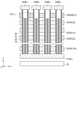
<1-2-2>動作波形
上述したように、本実施形態に係るメモリチップ100では、まず選択メモリセルMCのセレクタSWがオフ状態、非選択メモリセルMCのセレクタSWがオン状態となるような電圧をワード線WLに印加する。続いて、メモリチップ100は選択トランジスタSTがオンするような電圧をセレクトゲート線SGDに印加し、ビット線BLと、選択メモリセルMCが属するメモリピラーMPが導通状態となる。こうして電流は、非選択メモリセルMCにおいては、セレクタSWの半導体層内を流れ、選択メモリセルMCにおいては、記憶素子MRを流れる。<1-2-2> Operation waveform As described above, in the
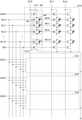
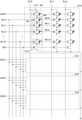
図14を用いて、本実施形態に係るメモリチップ100の動作波形について説明する。図14は、動作波形のタイミングチャートを示している。 The operating waveform of the
まず、読み出し動作について説明する。時刻T0において、シーケンサ170は、ビット線BLの電圧(ビット線電圧)及びソース線SLの電圧(ソース線電圧)をLow(“L”)レベルに維持し、ワード線WLの電圧をVMONに維持し、セレクトゲート線SGDの電圧をVSS(VSS<VMON)からVSON(VSS<VMON<VSON)に立ち上げる。Lレベルの電圧は、例えば、電圧VSSであってもよい。なお、図14の例では、時刻T0の前に、予め、ビット線BLの電圧及びソース線SLの電圧がLレベルとされ、ワード線WLの電圧がVMONとされ、セレクトゲート線SGDの電圧がVSSとされている。これに限定されず、例えば、時刻T0において、ワード線WLに電圧VMONが印加され、セレクトゲート線SGDに電圧VSSが印加されると同時に。セレクトゲート線SGDの電圧がVSSからVSONに立ち上げられてもよい。電圧VSSは、メモリセルMCのセレクタSW、または選択トランジスタSTをオフ状態にする電圧である。換言すると、電圧VSSは、ビット線BLの電圧の伝送をストップできる電圧である。電圧VMONは、メモリセルMCのセレクタSW、または選択トランジスタSTの半導体層32にチャネルを形成できる(強反転する)程度の電圧である。例えば、電圧VMONは、ソース線SLの電圧とセレクタSWの閾値電圧とを加えた電圧よりも大きい。電圧VSONは、メモリセルMCのセレクタSW、または選択トランジスタSTの半導体層32にチャネルを形成できる(強反転する)電圧である。また、電圧VSONは、メモリセルMCのセレクタSW、または選択トランジスタSTがビット線電圧を十分に転送できる程度の電圧である。電圧VSONは、ビット線に印加される電圧と、選択トランジスタの閾値電圧と、を加えた電圧よりも大きい。また、電圧VSONは、ビット線に印加される電圧と、セレクタSWの閾値電圧と、を加えた電圧よりも大きい。電圧VMONは、電圧VSS及び電圧VSONの中間の電圧である。例えば、電圧VSSは0Vであり、電圧VMONは2Vであり、電圧VSONは4Vである。なお、以下の説明では、ワード線WL及びセレクトゲート線SGD(及び後述するSGS)に、同じ電圧VSONを印加する場合について説明するが、ワード線WLに印加する電圧VSONと、セレクトゲート線SGD(及び後述するSGS)に印加する電圧VSONは、同じであってもよいし、異なっていてもよい。換言すれば、メモリセルMCのセレクタSWがビット線電圧を十分に転送できる程度の電圧と、選択トランジスタSTがビット線電圧を十分に転送できる程度の電圧とは、同じであってもよく、異なっていてもよい。 First, the read operation will be described. At time T0, the sequencer 170 maintains the voltage of the bit line BL (bit line voltage) and the voltage of the source line SL (source line voltage) at the Low (“L”) level, and maintains the voltage of the word line WL at VMON. Then, the voltage of the select gate line SGD is raised from VSS (VSS <VMON) to VSON (VSS <VMON <VSON). The L level voltage may be, for example, a voltage VSS. In the example of FIG. 14, before the time T0, the voltage of the bit line BL and the voltage of the source line SL are set to L level, the voltage of the word line WL is set to VSS, and the voltage of the select gate line SGD is set. It is said to be VSS. Not limited to this, for example, at time T0, the voltage VMON is applied to the word line WL and the voltage VSS is applied to the select gate line SGD at the same time. The voltage of the select gate line SGD may be raised from VSS to VSS. The voltage VSS is a voltage that turns off the selector SW of the memory cell MC or the selection transistor ST. In other words, the voltage VSS is a voltage that can stop the transmission of the voltage of the bit line BL. The voltage VMON is a voltage such that a channel can be formed (strongly inverted) in the selector SW of the memory cell MC or the
時刻T0の時点で、全てのメモリセルMCのセレクタSWはオン状態となる。 At time T0, the selector SWs of all memory cell MCs are turned on.
時刻T1の時点で、セレクトゲート線SGDの電圧はVMONとなる。この時点で、選択トランジスタST(1)はオン状態となり、ビット線BLと、メモリセルストリングMSと、が電気的に接続される。 At time T1, the voltage of the select gate line SGD becomes VMON. At this point, the selection transistor ST (1) is turned on, and the bit line BL and the memory cell string MS are electrically connected.
少なくともセレクトゲート線SGDの電圧がVMONに立ち上げられた時刻T1において、すなわち、セレクトゲート線SGDの電圧がVMONに立ち上げられると同時または立ち上げられた後に、シーケンサ170は、非選択ワード線WLの電圧をVMONからVSONに立ち上げ、選択ワード線WLの電圧をVMONからVSSに立ち下げる。 At least at the time T1 when the voltage of the select gate line SGD is started up in VSS, that is, at the same time as or after the voltage of the select gate line SGD is started up in VSS, the sequencer 170 is a non-selection word line WL. The voltage of the selected word line WL is raised from VMON to VSS, and the voltage of the selected word line WL is lowered from VMON to VSS.
時刻T2において、セレクトゲート線SGD、及び非選択ワード線WLの電圧がVSONになり、選択ワード線WLの電圧がVSSになる。これにより、時刻T2~時刻T4においては、選択されたメモリセルストリングMSのメモリセルMCのうち非選択メモリセルMCのセレクタSWがオン状態となり、選択メモリセルMCのセレクタSWがオフ状態となる。 At time T2, the voltage of the select gate line SGD and the non-selected word line WL becomes VSS, and the voltage of the selected word line WL becomes VSS. As a result, from time T2 to time T4, the selector SW of the non-selected memory cell MC among the memory cells MC of the selected memory cell string MS is turned on, and the selector SW of the selected memory cell MC is turned off.
時刻T2~T3の期間において、シーケンサ170は、選択ビット線BLの電圧をLレベルから読み出し電圧Vreadに立ち上げる。電圧Vreadは、Lレベルの電圧(例えば、電圧VSS)よりも高い電圧である。 During the period from time T2 to T3, the sequencer 170 raises the voltage of the selected bit line BL from the L level to the read voltage Vread. The voltage voltage is a voltage higher than the voltage of the L level (for example, voltage VSS).
時刻T3において、シーケンサ170は、ビット線BLに読み出し電圧Vreadを印加した後に、ビット線BLをフローティング状態にする。これにより、選択したメモリセルMCの記憶素子MRが、高抵抗状態(リセット)の時は、ビット線BLの電圧がゆっくり減衰し(時刻T4まで電圧が略維持される)、低抵抗状態(セット)の時はビット線BLの電圧が急速に減衰する。センスアンプ140は、センス動作として、例えば時刻T3においてビット線BLに読み出し電圧Vreadを印加して一定時間経過した後、例えば時刻T4においてビット線BLの電圧を参照電位と比較して、「Hレベル/Lレベル」をセンスする。参照電位は、例えば、Vread≧ビット線電圧(リセット)>参照電位>ビット線電圧(セット)の関係となるように設定される。 At time T3, the sequencer 170 puts the bit line BL in a floating state after applying a read voltage voltage to the bit line BL. As a result, when the memory element MR of the selected memory cell MC is in a high resistance state (reset), the voltage of the bit line BL is slowly attenuated (the voltage is substantially maintained until time T4), and is in a low resistance state (set). ), The voltage of the bit line BL rapidly decays. As a sense operation, the sense amplifier 140 applies a read voltage voltage to the bit line BL at time T3, elapses for a certain period of time, and then compares the voltage of the bit line BL with the reference potential at time T4, for example, to obtain "H level". / L level "is sensed. The reference potential is set so that, for example, the relationship of Vread ≧ bit line voltage (reset)> reference potential> bit line voltage (set).
時刻T5において、シーケンサ170は、セレクトゲート線SGDの電圧をVSONからVSSに立ち下げ、非選択ワード線WLの電圧をVSONからVMONに立ち下げ、選択ワード線WLの電圧をVSSからVMONに立ち上げる。 At time T5, the sequencer 170 lowers the voltage of the select gate line SGD from VSS to VSS, lowers the voltage of the non-selected word line WL from VSS to VMON, and raises the voltage of the selected word line WL from VSS to VMON. ..
時刻T6において、セレクトゲート線SGD、及びワード線WLの電圧はVMONとなる。全てのメモリセルMCのセレクタSWがオン状態となる。 At time T6, the voltages of the select gate line SGD and the word line WL become VMON. The selector SW of all memory cell MCs is turned on.
また、時刻T7において、セレクトゲート線SGDの電圧はVSSとなる。これにより、選択トランジスタST(1)がオフ状態となる。 Further, at time T7, the voltage of the select gate line SGD becomes VSS. As a result, the selection transistor ST (1) is turned off.
次に、書き込み動作について説明する。なお、セレクトゲート線SGD、ワード線WL、及びソース線SLの動作波形は、読み出し動作の場合と書き込み動作の場合とで同じである。これに対し、ビット線BLの動作波形は、読み出し動作の場合と書き込み動作の場合とで異なる。以下では、読み出し動作と異なる点、すなわちビット線の電圧を中心に説明する。 Next, the writing operation will be described. The operation waveforms of the select gate line SGD, the word line WL, and the source line SL are the same in the case of the read operation and the case of the write operation. On the other hand, the operation waveform of the bit line BL is different between the read operation and the write operation. In the following, the points different from the read operation, that is, the voltage of the bit line will be mainly described.
書き込み動作の場合、シーケンサ170は、時刻T2~T3の期間において、ビット線BLの電圧をLレベルから電圧Vwriteに立ち上げる。電圧Vwriteは、書き込み用のパルス電圧であり、Lレベルの電圧(例えば、電圧VSS)よりも高い電圧である。例えば、電圧Vwriteは、電圧Vreadよりも高い電圧である。シーケンサ170は、時刻T3~T3’の期間、ビット線BLに電圧Vwriteのパルスを印可する。 In the case of the writing operation, the sequencer 170 raises the voltage of the bit line BL from the L level to the voltage Vwite during the period from time T2 to T3. The voltage Vwrite is a pulse voltage for writing, which is higher than the L level voltage (for example, voltage VSS). For example, the voltage Vwite is a voltage higher than the voltage Vread. The sequencer 170 applies a voltage Vwrite pulse to the bit line BL during the period from time T3 to T3'.
例えば、時刻T3’~T4の期間において、ビット線BLの電圧がVwriteからLレベルに急峻に立ち下げられると、記憶素子MRは高抵抗なリセット状態とされる。また、時刻T3’~t4の期間において、ビット線BLの電圧がVwriteからLレベルに比較的ゆっくりと立ち下げられると、記憶素子MRは低抵抗なセット状態とされる。なお、時刻T3~t4の期間、すなわち書き込み期間、非選択のビット線BLはソース線SL電圧と同一(例えばLレベル)に保つ事が重要である。メモリセルMCはビット線BLに電圧を印加することで選択される。もしも非選択のビット線BLの電位が上げられると、誤選択となってしまい、誤書き込みとなってしまう。読み書きしたいビット線BLに対して選択的に電圧を印加すればよい。 For example, in the period from time T3'to T4, when the voltage of the bit line BL suddenly drops from Vwrite to the L level, the storage element MR is put into a high resistance reset state. Further, when the voltage of the bit line BL is relatively slowly lowered from Vwrite to the L level in the period from time T3'to t4, the storage element MR is put into a low resistance set state. It is important to keep the period from time T3 to t4, that is, the writing period, and the non-selected bit line BL the same as the source line SL voltage (for example, L level). The memory cell MC is selected by applying a voltage to the bit line BL. If the potential of the non-selected bit line BL is raised, erroneous selection will occur and erroneous writing will occur. A voltage may be selectively applied to the bit line BL to be read / written.
<1-3>効果
上述した実施形態によれば、メモリチップ100は、抵抗値に応じた1ビットもしくは複数ビットのデータ値を設定することが可能な記憶素子をメモリピラーMPの中心に配し、記憶素子の周辺を半導体層で覆い、更に其の周りを絶縁体層及びワード線WLで覆い、前記記憶素子の上端に選択トランジスタSTを介してビット線BLに接続し、前記記憶素子の下端に選択トランジスタSTを介さずにソース線SLを接続した構成を採る。<1-3> Effect According to the above-described embodiment, in the
ところで、半導体基板に対して垂直方向にメモリセルMCを積層し、高集積化を図る不揮発性メモリ(3次元NAND型フラッシュメモリ)として、BiCSTMが提案され市販されている。この3次元NAND型フラッシュメモリとは、平面構造のNAND型フラッシュメモリ(2次元NAND型フラッシュメモリ)を3次元化したものである。3次元NAND型フラッシュメモリは、2次元NAND型フラッシュメモリと同様に、書き換え回数の制約や、プログラムに要する時間が長い等の問題を有している。By the way, BiCSTM has been proposed and put on the market as a non-volatile memory (three-dimensional NAND flash memory) in which memory cell MCs are laminated in a direction perpendicular to a semiconductor substrate to achieve high integration. The three-dimensional NAND flash memory is a three-dimensional version of a planar NAND flash memory (two-dimensional NAND flash memory). Like the two-dimensional NAND flash memory, the three-dimensional NAND flash memory has problems such as restrictions on the number of rewrites and a long time required for programming.
3次元NAND型フラッシュメモリのメモリセルMCはシリコン並びにONO(Oxide-Nitride-Oxide)膜を備える。3次元NAND型フラッシュメモリは、ワード線WLに電圧を印加することで、メモリセルMCのシリコンを介して、メモリセルMCのONO膜の“N”に相当するSiNに、電子をトラップさせる。これによりメモリセルMCの閾値がシフトし、情報がメモリセルMCに記憶される。 The memory cell MC of the three-dimensional NAND flash memory includes silicon and an ONO (Oxide-Nitride-Oxide) film. In the three-dimensional NAND flash memory, by applying a voltage to the word line WL, electrons are trapped in SiN corresponding to “N” of the ONO film of the memory cell MC via the silicon of the memory cell MC. As a result, the threshold value of the memory cell MC shifts, and the information is stored in the memory cell MC.
他方で、上述した実施形態では、記憶素子MRのピラーを覆う様にセレクタSW(トランジスタ)のチャネル(半導体層32)が形成される。メモリセルMCの選択は、ワード線WLに選択または非選択に応じた電圧を供給し、選択ビット線BLに電圧を印加することでなされる。 On the other hand, in the above-described embodiment, the channel (semiconductor layer 32) of the selector SW (transistor) is formed so as to cover the pillar of the storage element MR. The selection of the memory cell MC is performed by supplying a voltage corresponding to selection or non-selection to the word line WL and applying a voltage to the selection bit line BL.
選択メモリセルMCのセレクタSWをオフ状態にし、非選択メモリセルMCのセレクタSWをオン状態にすると、選択メモリセルMCでは、電流が記憶素子MRを流れ、非選択メモリセルMCでは、電流が半導体層32を流れる。 When the selector SW of the selected memory cell MC is turned off and the selector SW of the non-selected memory cell MC is turned on, the current flows through the storage element MR in the selected memory cell MC, and the current flows in the non-selected memory cell MC. Flow through
上述した実施形態では、メモリチップ100は、選択メモリセルMCに記憶された情報を読み出すために、初期状態として、セレクトゲート線SGDの電圧をVSSとし、ワード線WLの電圧をVMONとする。そして、メモリチップ100は、セレクトゲート線の電圧をVSSからVSONに立ち上げる。そして、メモリチップ100は、少なくともセレクトゲート線SGDの電圧がVMONまで上がったあとで、選択ワード線WLの電圧をVMONからVSSに立ち下げ、非選択ワード線WLの電圧をVMONからVSONに立ち上げる。これにより、読み出し動作時及び書き込み動作時において、メモリセルストリングMSに生じるディスターブを抑制することができる。よって、記憶装置の信頼性を向上できる。 In the above-described embodiment, the
また、上述した実施形態では、メモリチップ100は、セレクトゲート線SGDの電圧をVSONからVSSに立ち下げ、選択ワード線WLの電圧をVSSからVMONに立ち上げ、非選択ワード線WLの電圧をVSONからVMONに立ち下げる。これにより、読み出し動作時及び書き込み動作時において、メモリセルストリングMSに生じるディスターブを抑制することができる。 Further, in the above-described embodiment, the
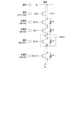
図15、及び図16を用いてメモリセルストリングMSに生じるディスターブを説明するために比較例について説明する。図15は、一つのメモリセルストリングMSを抜き出した回路図である。図15では、メモリセルMC(0)を選択する。図16は、比較例に係る読み出し動作の波形のタイミングチャートを示している。また、図16の例では、ノードCTD(0)とノードCTD(1)との電位差、及びノードCTD(15)とソース線SLとの電位差を示している。 A comparative example will be described with reference to FIGS. 15 and 16 in order to explain the stabilizer generated in the memory cell string MS. FIG. 15 is a circuit diagram obtained by extracting one memory cell string MS. In FIG. 15, memory cell MC (0) is selected. FIG. 16 shows a timing chart of the waveform of the read operation according to the comparative example. Further, in the example of FIG. 16, the potential difference between the node CTD (0) and the node CTD (1) and the potential difference between the node CTD (15) and the source line SL are shown.
図15では、選択トランジスタST(1)と、メモリセルMC(0)との間のノードをCTD(0)とラベルする。メモリセルMC(0)と、メモリセルMC(1)との間のノードをCTD(1)とラベルする。同様に他のメモリセルMC(n-1)と、メモリセルMC(n)との間のノードをCTD(n)とラベルする。 In FIG. 15, the node between the selection transistor ST (1) and the memory cell MC (0) is labeled as CTD (0). The node between the memory cell MC (0) and the memory cell MC (1) is labeled as CTD (1). Similarly, the node between the other memory cell MC (n-1) and the memory cell MC (n) is labeled as CTD (n).
ビット線BLの電圧をメモリセルストリングMSに転送する際に、メモリセルストリングMS内にディスターブが生じるおそれがある。 When the voltage of the bit line BL is transferred to the memory cell string MS, a disrupt may occur in the memory cell string MS.
例えば、図16では、時刻T10において、非選択ワード線WLをLレベル(例えば電圧VSS)からHレベル(例えば電圧VSON)に立ち上げてから、時刻T11において、セレクトゲート線SGDをLレベルからHレベルに立ち上げている。例えば、図15に示すように、メモリセルMC(0)を選択する場合、ノードCTD(0)の電位は、ワード線WL0がLレベルのため、他のノードCTD(1)~CTD(15)よりもワード線WLとのカップリング容量による電位の変化量(昇圧の幅)が小さい。これに対し、例えば、ノードCTD(1)の電位は、ワード線WL1とのカップリング容量によって比較的大きく昇圧される。このため、ノードCTD(0)の電位とノードCTD(1)との電位差(CTD(0)-CTD(1))が発生し、その結果、ノードCTD(0)と、ノードCTD(1)との電位差により、大きなディスターブが生じるおそれがある。 For example, in FIG. 16, at time T10, the non-selected word line WL is raised from the L level (for example, voltage VSS) to the H level (for example, voltage VSS), and then at time T11, the select gate line SGD is changed from the L level to H. Raised to the level. For example, as shown in FIG. 15, when the memory cell MC (0) is selected, the potential of the node CTD (0) is the other nodes CTD (1) to CTD (15) because the word line WL0 is at the L level. The amount of change in potential (width of boosting) due to the coupling capacitance with the word line WL is smaller than that. On the other hand, for example, the potential of the node CTD (1) is relatively greatly boosted by the coupling capacitance with the word line WL1. Therefore, a potential difference between the potential of the node CTD (0) and the node CTD (1) (CTD (0) -CTD (1)) is generated, and as a result, the node CTD (0) and the node CTD (1) Due to the potential difference of, a large disturb may occur.
また、図16の例では、時刻T12において、セレクトゲート線SGDをHレベルからLレベルに立ち下げてから、時刻T13において、非選択ワード線WLをHレベルからLレベルに立ち下げている。このとき、ノードCTD(0)~CTD(15)の電位は、対応するワード線WLとのカップリング容量によって、比較的大きく降圧される。これに対し、ソース線SLの電位は変動しない。このため、ノードCTD(15)の電位とソース線SLとの電位差(CTD(15)-SL)が、他のノードCTD間の電位差と比較した場合よりも大きくなる。例えば、ノードCTD(15)が降圧されるため、CTD(15)-SLは、負電圧側に変動する。その結果、ノードCTD(15)と、ソース線SLとの電位差により、比較的大きなディスターブが生じるおそれがある。 Further, in the example of FIG. 16, at time T12, the select gate line SGD is lowered from H level to L level, and then at time T13, the non-selected word line WL is lowered from H level to L level. At this time, the potentials of the nodes CTD (0) to CTD (15) are relatively greatly stepped down by the coupling capacitance with the corresponding word line WL. On the other hand, the potential of the source line SL does not fluctuate. Therefore, the potential difference between the potential of the node CTD (15) and the source line SL (CTD (15) -SL) is larger than the potential difference between the other node CTDs. For example, since the node CTD (15) is stepped down, the CTD (15) -SL fluctuates to the negative voltage side. As a result, a relatively large disturb may occur due to the potential difference between the node CTD (15) and the source line SL.
図16の例は、読み出し動作における動作波形を示している。図14の説明と同様に、セレクトゲート線SGD、ワード線WL、及びソース線SLの動作波形は、読み出し動作の場合と書き込み動作の場合とで同じである。このため、書き込み動作の場合も読み出し動作と同様に、比較的大きなディスターブが生じるおそれがある。なお、書き込み動作におけるビット線BLの電圧は、図14と同様である。より具体的には、例えば、時刻T11~T12の期間に、ビット線BLに電圧Vwriteのパルスが印可され、その後、ビット線BLの電圧がVwriteからLレベルに立ち下げられる。このとき、ビット線BLの電圧がVwriteからLレベルに急峻に立ち下げられると、記憶素子MRは高抵抗なリセット状態とされる。また、ビット線BLの電圧がVwriteからLレベルに比較的ゆっくりと立ち下げられると、記憶素子MRは低抵抗なセット状態とされる。 The example of FIG. 16 shows an operation waveform in a read operation. Similar to the description of FIG. 14, the operation waveforms of the select gate line SGD, the word line WL, and the source line SL are the same in the case of the read operation and the case of the write operation. Therefore, in the case of the write operation as well as the read operation, a relatively large disturb may occur. The voltage of the bit line BL in the writing operation is the same as in FIG. More specifically, for example, during the period from time T11 to T12, a pulse of voltage Vwrite is applied to the bit line BL, and then the voltage of the bit line BL is lowered from Vwrite to the L level. At this time, when the voltage of the bit line BL is sharply lowered from Vwite to the L level, the storage element MR is put into a high resistance reset state. Further, when the voltage of the bit line BL is lowered from Vwrite to the L level relatively slowly, the storage element MR is put into a low resistance set state.
ここで、本実施形態の効果を説明する。図14に示すように、本実施形態では、選択メモリセルMCに係るメモリセルストリングMSにおいて、全てのメモリセルMCのセレクタSWをオン状態にしている。そして、ワード線WLの電圧を変動させる前に、セレクトゲート線SGDをVSSから立ち上げている(時刻T0~T1)。そして、少なくともセレクトゲート線SGDの電圧がVMONまで上がり、選択トランジスタST(1)がオン状態となり、ノードCTD(0)とビット線BLとが電気的に接続されたのち、選択ワード線WLをVSSに立ち下げ、非選択ワード線WLをVSONに立ち上げる。これにより、選択メモリセルMC(0)のセレクタSWをオフ状態にする前に、ノードCTD(1)と、ノードCTD(0)と、ビット線BLとが電気的に接続されている。そのため、ノードCTD(0)とCTD(1)間において比較例のようなカップリングに起因する電位の昇圧を抑制できる。その結果、ノードCTD(0)と、ノードCTD(1)との電位差を抑制でき、ディスターブを抑制できる。 Here, the effect of this embodiment will be described. As shown in FIG. 14, in the present embodiment, in the memory cell string MS related to the selected memory cell MC, the selector SWs of all the memory cell MCs are turned on. Then, before changing the voltage of the word line WL, the select gate line SGD is started up from VSS (time T0 to T1). Then, at least the voltage of the select gate line SGD rises to VMON, the selection transistor ST (1) is turned on, the node CTD (0) and the bit line BL are electrically connected, and then the selection word line WL is VSSed. The non-selected word line WL is started up in VSS. As a result, the node CTD (1), the node CTD (0), and the bit line BL are electrically connected before the selector SW of the selected memory cell MC (0) is turned off. Therefore, it is possible to suppress the increase in potential caused by the coupling as in the comparative example between the node CTD (0) and the CTD (1). As a result, the potential difference between the node CTD (0) and the node CTD (1) can be suppressed, and the disturb can be suppressed.
また、本実施形態では、セレクトゲート線SGDを立ち下げるとともに、選択ワード線WLを立ち上げ、非選択ワード線WLを立ち下げる。前記動作により、各ワード線WLの電位が変動している期間の大部分の期間、各ノードCTD間、ノードCTD(0)とビット線BLとの間、及びノードCTD(15)とソース線SLとの間が導通している事で、各ノード間に電位差が生じるのを抑制できる。その結果、比較例のようなディスターブを抑制できる。 Further, in the present embodiment, the select gate line SGD is turned down, the selected word line WL is started, and the non-selected word line WL is turned down. Due to the above operation, most of the period during which the potential of each word line WL is fluctuating, between each node CTD, between node CTD (0) and bit line BL, and between node CTD (15) and source line SL. Since there is continuity between the nodes, it is possible to suppress the occurrence of a potential difference between the nodes. As a result, the disturb as in the comparative example can be suppressed.
<1-4>変形例1
図17~図20を用いて、第1実施形態の変形例1について説明する。図17は、第1実施形態の変形例1に係るメモリセルアレイ110の回路構成を示している。図18は、第1実施形態の変形例1に係るメモリチップ100の備えるメモリセルアレイ110の断面構造の一例を示している。図19は、図18のA-A線に沿った平面図である。図20は、メモリセルアレイ110において一つのメモリセルストリングMSを抜き出した回路図である。<1-4>
A
図17に示すように、選択トランジスタST(1)と並列に接続された記憶素子MRが設けられてもよい。選択トランジスタST(1)と記憶素子MRとが並列に接続された構成は、メモリセルMCと同じ構成であってもよい。より具体的には、例えば、図18及び図19に示すように、第1選択トランジスタST(1)に対応するメモリピラーMPの領域内に、コア部材30及び抵抗変化層31が設けられてもよい。すなわち、コア部材30及び抵抗変化層31の上端が、導電体層23(セレクトゲート線SGD)よりも上方(ビット線側)に位置するように、コア部材30及び抵抗変化層31が設けられてもよい。他の構成は、第1実施形態と同様である。 As shown in FIG. 17, a storage element MR connected in parallel with the selection transistor ST (1) may be provided. The configuration in which the selection transistor ST (1) and the storage element MR are connected in parallel may be the same configuration as the memory cell MC. More specifically, for example, as shown in FIGS. 18 and 19, even if the
次に、動作の概要について説明する。
図20に示すように、第1実施形態の図12と同様に、選択したいメモリセルMC(例えばMC(2))が属するメモリピラーMPに接する選択トランジスタST(1)のセレクトゲート線SGDに所定の電圧(正の電圧)を印加する。これにより、選択トランジスタST(1)の半導体層32に反転層が形成され、電流が流れることができる状態となる(オン状態)。これにより、ビット線BLと、選択トランジスタST(1)と、選択トランジスタST(1)に接するメモリピラーMPの半導体層32が導通される。更に、選択メモリセルMC(2)に対応するワード線WL(2)には、例えば0[V]または電圧VSSを印加し、非選択メモリセルMCに対応するワード線WL(0)、(1)、(3)~(15)には所定の電圧(正の電圧)を印加する。これにより、ビット線BLとソース線SLと間を流れる電流パスは、選択したいメモリセルMC(2)においては、記憶素子MRを流れ、非選択のメモリセルMC(0)、(1)、(3)~(15)においては、セレクタSWの半導体層32を流れる。Next, the outline of the operation will be described.
As shown in FIG. 20, similarly to FIG. 12 of the first embodiment, it is predetermined to the select gate line SGD of the selection transistor ST (1) in contact with the memory pillar MP to which the memory cell MC (for example, MC (2)) to be selected belongs. Voltage (positive voltage) is applied. As a result, an inversion layer is formed on the
本変形例においても、第1実施形態と同様の効果が得られる。 Also in this modification, the same effect as that of the first embodiment can be obtained.
<2>第2実施形態
<2-1>概要
続いて、第2実施形態について説明する。上述した実施形態では、ソース線SLとして導電体層を半導体基板と平行に配した。しかし、第2実施形態ではソース線SLに相当する導電体層を半導体層(Pwell)にし、ソース線SLと、メモリセルとの間に選択トランジスタST(2)を設けている。以下、第1実施形態と異なる点を中心に説明する。<2> Second Embodiment <2-1> Outline Next, the second embodiment will be described. In the above-described embodiment, the conductor layer is arranged in parallel with the semiconductor substrate as the source wire SL. However, in the second embodiment, the conductor layer corresponding to the source line SL is a semiconductor layer (Pwell), and the selection transistor ST (2) is provided between the source line SL and the memory cell. Hereinafter, the points different from those of the first embodiment will be mainly described.
<2-2>メモリセルアレイ110の回路構成
第2実施形態に係るメモリセルアレイ110の回路構成(等価回路)について図21を用いて説明する。<2-2> Circuit Configuration of
図21に示すように、図2に示す回路と比較し、メモリセルストリングMSの各々は、例えば16個のメモリセルMC(MC(0)~MC(15))、及び選択トランジスタST(1)に加え、記憶素子MRが並列に接続された選択トランジスタST(2)を更に含んでいる。記憶素子MRと選択トランジスタST(1)とが並列に接続された構成は、メモリセルMCと同じ構成であってもよい。以下、選択トランジスタST(2)と並列に接続された記憶素子MRについては、限定しない場合、その説明を省略する。 As shown in FIG. 21, in comparison with the circuit shown in FIG. 2, each of the memory cell string MSs has, for example, 16 memory cells MC (MC (0) to MC (15)) and a selection transistor ST (1). In addition, the storage element MR further includes a selection transistor ST (2) connected in parallel. The configuration in which the storage element MR and the selection transistor ST (1) are connected in parallel may be the same configuration as the memory cell MC. Hereinafter, if the storage element MR connected in parallel with the selection transistor ST (2) is not limited, the description thereof will be omitted.
各メモリセルストリングMSに含まれたメモリセルMC(0)~MC(15)は、選択トランジスタST(1)と選択トランジスタST(2)(及び選択トランジスタST(2)と並列に接続された記憶素子MR)との間に直列接続されている。 The memory cells MC (0) to MC (15) included in each memory cell string MS are stored in parallel with the selection transistor ST (1) and the selection transistor ST (2) (and the selection transistor ST (2). It is connected in series with the element MR).
ブロックBLK内の複数の選択トランジスタST(2)のゲートはセレクトゲート線SGSに共通に接続される。なお、セレクトゲート線SGSは、ストリングユニットSU毎に設けられてもよい。 The gates of the plurality of selection transistors ST (2) in the block BLK are commonly connected to the select gate line SGS. The select gate line SGS may be provided for each string unit SU.
以下、セレクトゲート線SGD(SGD(0)、SGD(1)、…)のそれぞれを限定しない場合は、セレクトゲート線SGDと表記する。 Hereinafter, when each of the select gate line SGD (SGD (0), SGD (1), ...) Is not limited, it is referred to as the select gate line SGD.
セレクトゲート線SGD及びSGSの各々、並びにワード線WLの各々は、ロウデコーダ120によって独立に制御される。 Each of the select gate lines SGD and SGS, and each of the word lines WL is independently controlled by the
また、メモリセルアレイ110内において同一列にあるメモリセルストリングMSの選択トランジスタST(2)のドレインは、メモリセルMC(15)のソースに接続され、選択トランジスタST(2)のソースは、ソース線SLに共通に接続されている。同様に、選択トランジスタST(2)と並列に接続された記憶素子MRの一端は、メモリセルMC(15)のソースに接続され、記憶素子MRの他端は、ソース線SLに共通に接続されている。 Further, the drain of the selection transistor ST (2) of the memory cell string MS in the same row in the
選択トランジスタST(2)のセレクトゲート線SGSをHレベルにすることで、選択トランジスタST(2)の半導体層32並びに半導体基板に反転層が形成され、ソース線SLに電流が流れる。 By setting the select gate line SGS of the selection transistor ST (2) to H level, an inversion layer is formed on the
<2-3>メモリセルアレイ110の構造
以下に、第2実施形態におけるメモリセルアレイ110の構造の一例について説明する。第2実施形態では半導体基板上に、選択トランジスタST(2)を設ける。選択トランジスタST(2)がオン状態となることで、半導体基板のPwell領域に反転層が形成され、半導体基板に設けられたN型拡散層を介して、ソース線SLに電流が流れる。なお、第1実施形態と同様に、ソース線SLとして機能する導電体層21が、半導体基板20の上方に設けられていてもよい。この場合、第1実施形態と同様に、コア部材30、抵抗変化層31、半導体層32、及び絶縁体層33の底面は、導電体層21に接する。<2-3> Structure of the
図22は、第2実施形態に係るメモリチップ100の備えるメモリセルアレイ110の断面構造の一例を示している。図22に示すように、具体的には、半導体基板40の表面領域に、Pwell領域41が設けられ、また、Pwell領域41内にN型拡散層(N+拡散層)42が設けられる。半導体基板40は、例えばXY平面に沿って広がった板状に形成され、シリコン(Si)を含んでいる。FIG. 22 shows an example of the cross-sectional structure of the
Pwell領域41上には、絶縁体層を介して導電体層(電位印加電極、電圧印加電極)25が設けられる。導電体層25は、例えばXY平面に沿って広がった板状に形成され、セレクトゲート線SGSとして機能する。導電体層25は、例えばタングステン(W)を含んでいる。 A conductor layer (potential application electrode, voltage application electrode) 25 is provided on the
また、N型拡散層42上には、導電体層26が設けられる。導電体層26は、例えばZY平面に沿って広がった板状に形成され、ソース線SLとして機能する。導電体層26は、例えばタングステン(W)を含んでいる。 Further, a
なお、選択トランジスタST(2)は、導電体層25、半導体層32、Pwell領域41を含む。導電体層25がHレベルとなることで、半導体層32、及びPwell領域41に反転層が形成され、電流が流れることが可能となる。 The selective transistor ST (2) includes a
導電体層25の上方に、絶縁体層と導電体層22とが交互に積層される。導電体層22は、例えばXY平面に沿って広がった板状に形成される。例えば、積層された複数の導電体層22は、半導体基板40側から順に、それぞれワード線WL(15)~WL(0)として使用される。導電体層22は、例えばタングステン(W)を含んでいる。 The insulator layer and the
最上層の導電体層22(WL(0))の上方に、絶縁体層を介して例えば導電体層23が積層される。導電体層23は、Y方向に延伸し、X方向において、後述するセレクトピラーSPごとに分断されている。分断された導電体層23は、それぞれセレクトゲート線SGD(0)~(3)として使用される。導電体層23は、例えばタングステン(W)を含んでいる。 For example, the
導電体層23の上方に、導電体層24が設けられる。例えば導電体層24は、X方向に沿って延伸したライン状に形成され、ビット線BLとして使用される。導電体層24は、例えば銅(Cu)を含んでいる。 The
次に、図23を用いて、導電体層23の平面図について説明する。図23は、図22のA1-A1線に沿った平面図である。図23では、Pwell領域41内の拡散層に集められた電流が板状のソース線SLに集められ、最上層まで上った後にソース線ドライバ(図示せず)に流れる事を表している。 Next, a plan view of the
次に、図24を用いて、Z方向におけるメモリセルMC間の平面図について説明する。図24は、図22のB1-B1線に沿った平面図である。図24は、メモリセルMC間のメモリピラーを示しており、半導体基板40と直交する板状のソース線SLがある点が第1実施形態と異なる。なお、図24に示すソース線SLは、Pwell領域41中の拡散層で集められた電流を上層まで上げる途中の経路である。 Next, a plan view between the memory cells MC in the Z direction will be described with reference to FIG. 24. FIG. 24 is a plan view taken along the line B1-B1 of FIG. 22. FIG. 24 shows the memory pillars between the memory cells MC, and is different from the first embodiment in that there is a plate-shaped source line SL orthogonal to the
次に、図25を用いて、導電体層22の平面図について説明する。図25は、図22のC1-C1線に沿った平面図である。図25は、半導体基板40と直交する板状のソース線SLがある点が、第1実施形態と異なる。なお、図25に示すソース線SLは、Pwell領域41中の拡散層で集められた電流を上層まで上げる途中の経路である。 Next, a plan view of the
次に、図26を用いて、Pwell領域41の平面図について説明する。図26は、図22のD1-D1線に沿った平面図である。図26に示すように、ビット線BLからメモリピラーMP中を下に向かって進んだ電流は、Pwell領域41に達した後、オン状態の選択トランジスタST(2)によりPwell領域41に反転層が出来ているために、反転層を流れ、拡散層42まで達する。この後、電流はソース線SLに入り、上まで進んだ後、ソース線ドライバ(図示せず)へと流れる。 Next, a plan view of the
次に、図27を用いて、メモリセルアレイ110の断面構造の一例について説明する。図27は、図22のE1-E1線に沿った断面図である。図27は、図22と直交する方向の断面である。図27及び図22を併せて参照すると、メモリピラーMPは、コア部材30を中心に同心円状の形状をしている事が分かる。 Next, an example of the cross-sectional structure of the
第2実施形態の効果として、第1実施形態と比較して、最下層に導電体層のソース線SLを設ける工程を省略出来、最下層のセレクトゲート線SGSは、ワード線WLと同様の工程で作る事により、プロセスの容易化が見込まれる。 As an effect of the second embodiment, as compared with the first embodiment, the step of providing the source wire SL of the conductor layer in the lowermost layer can be omitted, and the select gate wire SGS of the lowermost layer is the same process as the word wire WL. It is expected that the process will be easier by making it with.
<2-4>動作
<2-4-1>概要
続いて、第2実施形態に係るメモリチップ100の動作の概要について説明する。<2-4> Operation <2-4-1> Outline Next, an outline of the operation of the
第2実施形態に係るメモリチップ100において、読み出し動作及び書き込み動作は、ビット線BLと、ソース線SLと、の間に電流を流すことによって行う。 In the
図28及び図29を用いて、読み出し動作または書き込み動作を行うメモリセルMCを選択する方法について概略的に説明する。図28は、一つのメモリセルストリングMSを抜き出した回路図である。図29は、一つのメモリセルストリングMSに対応するメモリピラーMPを抜き出した断面図である。 A method of selecting a memory cell MC to perform a read operation or a write operation will be schematically described with reference to FIGS. 28 and 29. FIG. 28 is a circuit diagram obtained by extracting one memory cell string MS. FIG. 29 is a cross-sectional view of a memory pillar MP corresponding to one memory cell string MS.
図28及び図29に示すように、選択したいメモリセルMC(例えばMC(2))が属するメモリピラーMPに接する選択トランジスタST(1)のセレクトゲート線SGD及び選択トランジスタST(2)のセレクトゲート線SGSに所定の電圧(正の電圧)を印加する。これにより、選択トランジスタST(1)及びST(2)の半導体層32に反転層が形成され、電流が流れることができる状態となる(オン状態)。これにより、ビット線BLと、選択トランジスタST(1)と、選択トランジスタST(1)に接するメモリピラーMPの半導体層32と、選択トランジスタST(2)と、ソース線SLとが導通される。更に、選択メモリセルMC(2)に対応するワード線WL(2)には、例えば0[V]または電圧VSSを印加し、非選択メモリセルMCに対応するワード線WL(0)、(1)、(3)~(15)には所定の電圧(正の電圧)を印加する。これにより、ビット線BLとソース線SLと間を流れる電流パスは、選択したいメモリセルMC(2)においては、記憶素子MRを流れ、非選択のメモリセルMC(0)、(1)、(3)~(15)においては、セレクタSWの半導体層32を流れる。図29に示すように、メモリピラーMPの中心部分には絶縁体層であるコア部材30が設けられているので、選択メモリセルMCにおいて電流は、コア部材30を取り囲む抵抗変化層31を流れる。また、選択トランジスタST(2)のセレクトゲート線SGSに所定の電圧を印加する。これにより、選択トランジスタST(2)の半導体層32に反転層が形成され、電流が流れることができる状態となる(オン状態)。これにより、ビット線BLと、選択トランジスタST(1)と、選択トランジスタST(1)に接するメモリピラーMPの半導体層32と、選択トランジスタST(2)と、ソース線SLと、が導通される。 As shown in FIGS. 28 and 29, the select gate line SGD of the selection transistor ST (1) and the select gate of the selection transistor ST (2) in contact with the memory pillar MP to which the memory cell MC (for example, MC (2)) to be selected belongs. A predetermined voltage (positive voltage) is applied to the wire SGS. As a result, an inversion layer is formed on the
このようにする事で、読み出し動作時、書き込み動作時、共に抵抗変化層31を選択出来る様にする。本方式を3次元NAND型フラッシュメモリと比較した場合、より低電圧、且つより高速で動作出来る様になる他、書き換え回数の制約も少なく、書き込み時間も短くて済む利点がある。 By doing so, the
<2-4-2>動作波形
図30を用いて、第2の実施形態に係るメモリチップ100の動作波形について説明する。図30は、動作波形のタイミングチャートを示している。<2-4-2> Operation Waveform The operation waveform of the
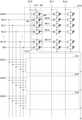
まず、読み出し動作の一例について説明する。時刻T20において、シーケンサ170は、ビット線BLの電圧(ビット線電圧)、及びソース線SLの電圧(ソース線電圧)をLレベルに維持し、ワード線WLの電圧をVSSに維持し、セレクトゲート線SGD、及びSGSの電圧を、VSSからVSONに立ち上げる。つまり、時刻T20の時点で、全てのメモリセルMCのセレクタSWはオフ状態となっている。 First, an example of the read operation will be described. At time T20, the sequencer 170 maintains the voltage of the bit line BL (bit line voltage) and the voltage of the source line SL (source line voltage) at the L level, maintains the voltage of the word line WL at the VSS, and selects the gate. The voltage of the wire SGD and SGS is raised from VSS to VSON. That is, at the time of time T20, the selector SWs of all the memory cell MCs are in the off state.
時刻T21の時点で、セレクトゲート線SGD、及びSGSの電圧はVMONとなる。この時点で、選択トランジスタST(1)及びST(2)はオン状態となる。 At time T21, the voltages of the select gate line SGD and SGS become VMON. At this point, the selection transistors ST (1) and ST (2) are turned on.
少なくともセレクトゲート線SGD、及びSGSの電圧がVMONに立ち上げられた時刻T21において、シーケンサ170は、ワード線WLをVSSからVSONに立ち上げる。 At least at the time T21 when the voltage of the select gate line SGD and the SGS is raised to VSS, the sequencer 170 raises the word line WL from VSS to VSS.
少なくともワード線WLの電圧がVSONに立ち上げられた時刻T22において、シーケンサ170は、非選択ワード線WLの電圧をVSONに維持し、選択ワード線WLの電圧をVSONからVSSに立ち下げる。セレクトゲート線SGD及びセレクトゲート線SGSの電圧がVSONに立ち上がった後にワード線WLの電圧を立ち上げ始めてもよい。 At least at the time T22 when the voltage of the word line WL is raised to VSS, the sequencer 170 maintains the voltage of the non-selected word line WL at VSS and lowers the voltage of the selected word line WL from VSS to VSS. After the voltage of the select gate line SGD and the select gate line SGS rises to VSON, the voltage of the word line WL may start to rise.
時刻T23において、セレクトゲート線SGD、及びSGS、非選択ワード線WLの電圧がVSONになり、選択ワード線WLの電圧がVSSになる。これにより、時刻T23~時刻T27においては、選択されたメモリセルストリングMSのメモリセルMCのうち非選択メモリセルMCのセレクタSWがオフ状態となる。 At time T23, the voltage of the select gate line SGD, SGS, and the non-selected word line WL becomes VSS, and the voltage of the selected word line WL becomes VSS. As a result, from time T23 to time T27, the selector SW of the non-selected memory cell MC among the memory cell MCs of the selected memory cell string MS is turned off.
時刻T21~T22の期間に選択ワード線WLの電圧と非選択ワード線WLの電圧とを同時に立ち上げる事により、選択ワード線WLによるカップリングの影響と非選択ワード線WLによるカップリングの影響とが同等となる。この結果、各電極間(各ノード間)にはカップリングによる電位差がほとんど生じない。 By raising the voltage of the selected word line WL and the voltage of the non-selected word line WL at the same time during the period from time T21 to T22, the influence of the coupling by the selected word line WL and the influence of the coupling by the non-selected word line WL can be obtained. Is equivalent. As a result, there is almost no potential difference due to coupling between each electrode (between each node).
また、時刻T22~T23の期間に、非選択ワード線WLの電圧を立ち下げずに、選択ワード線WLの電圧を立ち下げる。このとき、選択トランジスタST(1)及びST(2)並びに非選択メモリセルMCのセレクタSWが全て導通している。このため、カップリングによる電圧ノイズ(以下、「カップリングノイズ」とも表記する)は、ビット線BL及びソース線SLに速やかに吸収される(放電される)。従って、各電極間にはカップリングによる電位差がほとんど生じない。 Further, during the period from time T22 to T23, the voltage of the selected word line WL is reduced without lowering the voltage of the non-selected word line WL. At this time, the selection transistors ST (1) and ST (2) and the selector SW of the non-selection memory cell MC are all conducting. Therefore, the voltage noise due to the coupling (hereinafter, also referred to as “coupling noise”) is quickly absorbed (discharged) by the bit line BL and the source line SL. Therefore, there is almost no potential difference due to coupling between the electrodes.
時刻T24において、シーケンサ170は、選択ビット線BLの電圧をLレベルから電圧Vreadに立ち上げる。 At time T24, the sequencer 170 raises the voltage of the selected bit line BL from the L level to the voltage Vread.
時刻T25において、シーケンサ170は、ビット線BLに読み出し電圧Vreadを印加した後に、ビット線BLをフローティング状態にする。これにより、選択したメモリセルMCが、高抵抗状態(リセット)の時は、ビット線BLの電圧がゆっくり減衰し、低抵抗状態(セット)の時はビット線BLの電圧が急速に減衰する。センスアンプ140は、センス動作として、ビット線BLに読み出し電圧Vreadを印加して一定時間経過した後、例えば時刻T26において、ビット線BLの電圧を参照電位と比較して、「Hレベル/Lレベル」をセンスする。 At time T25, the sequencer 170 puts the bit line BL in a floating state after applying a read voltage voltage to the bit line BL. As a result, when the selected memory cell MC is in the high resistance state (reset), the voltage of the bit line BL is slowly attenuated, and when the selected memory cell MC is in the low resistance state (set), the voltage of the bit line BL is rapidly attenuated. As a sense operation, the sense amplifier 140 applies a read voltage voltage to the bit line BL, elapses for a certain period of time, and then, for example, at time T26, compares the voltage of the bit line BL with the reference potential to obtain "H level / L level". ”.
時刻T27において、シーケンサ170は、選択ワード線WLの電圧をVSSからVSONに立ち上げる。 At time T27, the sequencer 170 raises the voltage of the selected word line WL from VSS to VSS.
選択ワード線WLの電圧がVSONに立ち上がった時刻T28において、シーケンサ170は、セレクトゲート線SGD及びSGSの電圧をVSONからVSSに立ち下げ、ワード線WLの電圧をVSONからVSSに立ち下げる。 At the time T28 when the voltage of the selected word line WL rises to VSS, the sequencer 170 lowers the voltage of the select gate lines SGD and SGS from VSS to VSS, and lowers the voltage of the word line WL from VSS to VSS.
時刻T29において、選択トランジスタST(1)及びST(2)と、全てのメモリセルMCのセレクタSWがオフ状態となる。 At time T29, the selection transistors ST (1) and ST (2) and the selector SWs of all the memory cell MCs are turned off.
時刻T27~T28の期間において、選択ワード線WLの電圧の立ち上げに伴うカップリングノイズは、選択トランジスタST(1)及びST(2)並びに非選択メモリセルMCのセレクタSWが全て導通しているためにビット線BL及びソース線SLに速やかに吸収される。このため、カップリングノイズの影響は、比較的小さい。 During the period from time T27 to T28, the coupling noise caused by the rise of the voltage of the selected word line WL is all conducted by the selective transistors ST (1) and ST (2) and the selector SW of the non-selected memory cell MC. Therefore, it is quickly absorbed by the bit line BL and the source line SL. Therefore, the influence of coupling noise is relatively small.
また、時刻T28~T29の期間において、選択ワード線WLの電圧は、セレクトゲート線SGD及びSGS、並びに非選択ワード線WLと共に立ち下げられる。このため、各電極間におけるカップリングノイズの影響は等しくなり、記憶素子MRの両電極間に電位差はほとんど生じない。 Further, during the period from time T28 to T29, the voltage of the selected word line WL is lowered together with the select gate lines SGD and SGS, and the non-selected word line WL. Therefore, the influence of the coupling noise between the electrodes is equal, and there is almost no potential difference between the two electrodes of the storage element MR.
次に、書き込み動作について説明する。第1実施形態の図14の説明と同様に、セレクトゲート線SGD及びSGS、ワード線WL、並びにソース線SLの動作波形は、読み出し動作の場合と書き込み動作の場合とで同じである。書き込み動作の場合、シーケンサ170は、時刻T24~T25の期間において、ビット線BLの電圧をLレベルから電圧Vwriteに立ち上げる。次に、シーケンサ170は、時刻T25~T25’の期間、ビット線BLに電圧Vwriteのパルスを印可する。 Next, the writing operation will be described. Similar to the description of FIG. 14 of the first embodiment, the operation waveforms of the select gate lines SGD and SGS, the word line WL, and the source line SL are the same in the case of the read operation and the case of the write operation. In the case of the writing operation, the sequencer 170 raises the voltage of the bit line BL from the L level to the voltage Vwrite during the period from time T24 to T25. Next, the sequencer 170 applies a pulse of voltage Vwite to the bit line BL during the period from time T25 to T25'.
例えば、時刻T25’~T26の期間において、ビット線BLの電圧がVwriteからLレベルに急峻に立ち下げられると、記憶素子MRは高抵抗なリセット状態とされる。また、時刻T25’~t26の期間において、ビット線BLの電圧がVwriteからLレベルに比較的ゆっくりと立ち下げられると、記憶素子MRは低抵抗なセット状態とされる。 For example, in the period from time T25'to T26, when the voltage of the bit line BL is sharply lowered from Vwrite to the L level, the storage element MR is put into a high resistance reset state. Further, in the period from time T25'to t26, when the voltage of the bit line BL is lowered from Vwrite to the L level relatively slowly, the storage element MR is put into a low resistance set state.
なお、読み出し動作の例は、これに限定されない。例えば、第1実施形態の図14において、セレクトゲート線SGDと同じ電圧をセレクトゲート線SGSに印加してもよいし、図16においてセレクトゲート線SGDと同じ電圧をセレクトゲート線SGSに印加してもよい。 The example of the read operation is not limited to this. For example, in FIG. 14 of the first embodiment, the same voltage as the select gate wire SGS may be applied to the select gate wire SGS, or the same voltage as the select gate wire SGS in FIG. 16 may be applied to the select gate wire SGS. May be good.
例えば、図14の時刻T0において、シーケンサ170は、セレクトゲート線SGD及びSGSの電圧をVSSからVSONに立ち上げる。時刻T1の時点で、セレクトゲート線SGD及びSGSの電圧がVMONまで立ち上げられた後、シーケンサ170は、非選択ワード線WLの電圧をVMONからVSONに立ち上げ、選択ワード線WLの電圧をVMONからVSSに立ち下げる。時刻T2において、セレクトゲート線SGD及びSGS、及び非選択ワード線WLの電圧がVSONになり、選択ワード線WLの電圧がVSSになる。そして、時刻T5において、シーケンサ170は、セレクトゲート線SGD及びSGSの電圧をVSONからVSSに立ち下げ、非選択ワード線WLの電圧をVSONからVMONに立ち下げ、選択ワード線WLの電圧をVSSからVMONに立ち上げる。 For example, at time T0 in FIG. 14, the sequencer 170 raises the voltages of the select gate lines SGD and SGS from VSS to VSS. At time T1, after the voltages of the select gate lines SGD and SGS are raised to VMON, the sequencer 170 raises the voltage of the non-selected word line WL from VMON to VSS and the voltage of the selected word line WL to VSS. To VSS. At time T2, the voltage of the select gate lines SGD and SGS and the non-selected word line WL becomes VSS, and the voltage of the selected word line WL becomes VSS. Then, at time T5, the sequencer 170 lowers the voltage of the select gate lines SGD and SGS from VSS to VSS, lowers the voltage of the non-selected word line WL from VSS to VMON, and causes the voltage of the selected word line WL from VSS. Launch to VMON.
<2-5>効果
上述した実施形態によれば、メモリチップ100は、選択メモリセルMCに記憶された情報を読み出すため、または選択メモリセルMCに情報を記憶させるために、セレクトゲート線SGD、及びSGSの電圧をVSSからVSONに立ち上げる。そして、メモリチップ100は、少なくともセレクトゲート線SGD、及びSGSの電圧がVMONまで上がったあとで、ワード線WLの電圧をVSSからVSONに立ち上げる。そして、選択ワード線WLの電圧は、セレクトゲート線SGD及びSGS、並びに非選択ワード線WLが全てオン状態とされ、選択トランジスタST(1)及びST(2)並びに非選択メモリセルMCのセレクタSWが導通した後に、立ち下げを開始する。選択ワード線WLの電圧の立ち下げ期間の大部分の期間、選択トランジスタST(1)及びST(2)並びに非選択メモリセルMCのセレクタSWは導通している。このため、記憶素子MRの両電極間に電位差が生じにくく、ディスターブが低減される。これにより、読み出し動作時及び書き込み動作時において、メモリセルストリングMSに生じるディスターブを抑制することができる。<2-5> Effect According to the above-described embodiment, the
図31を用いてメモリセルストリングMSに生じるディスターブを説明するために比較例について説明する。図31は、一つのメモリセルストリングMSを抜き出した回路図である。図31では、メモリセルMC(0)を選択する。 A comparative example will be described in order to explain the disruption that occurs in the memory cell string MS with reference to FIG. 31. FIG. 31 is a circuit diagram obtained by extracting one memory cell string MS. In FIG. 31, the memory cell MC (0) is selected.
図31では、選択トランジスタST(2)と、メモリセルMC(15)との間のノードをCTD(SL)とラベルする。 In FIG. 31, the node between the selection transistor ST (2) and the memory cell MC (15) is labeled as CTD (SL).
ビット線BLの電圧をメモリセルストリングMSに転送する際に、メモリセルストリングMS内にディスターブが生じるおそれがある。 When the voltage of the bit line BL is transferred to the memory cell string MS, a disrupt may occur in the memory cell string MS.
例えば、図16と同様に、図31の回路図において、セレクトゲート線SGD及びSGSをHレベル(例えば電圧VSON)からLレベル(例えば電圧VSS)に立ち下げてから、非選択ワード線WLをHレベルからLレベルに立ち下げた場合を考える。例えば、図31に示すように、メモリセルMC(0)を選択する場合において、ノードCTD(15)の電位は、ワード線WL15とのカップリング容量によって、比較的大きく下降する。これに対し、セレクトゲート線SGSはLレベルのため、ノードCTD(SL)の電位の変化量は比較的小さい。このため、ノードCTD(15)とノードCTD(SL)との電位差が、発生する。ノードCTD(15)と、ノードCTD(SL)との電位差により、大きなディスターブが生じるおそれがある。 For example, as in FIG. 16, in the circuit diagram of FIG. 31, the select gate lines SGD and SGS are lowered from the H level (for example, voltage VSON) to the L level (for example, voltage VSS), and then the non-selected word line WL is changed to H. Consider the case of dropping from level to L level. For example, as shown in FIG. 31, when the memory cell MC (0) is selected, the potential of the node CTD (15) drops relatively significantly due to the coupling capacitance with the word line WL15. On the other hand, since the select gate line SGS is at the L level, the amount of change in the potential of the node CTD (SL) is relatively small. Therefore, a potential difference between the node CTD (15) and the node CTD (SL) is generated. A large disturb may occur due to the potential difference between the node CTD (15) and the node CTD (SL).
また、本実施形態では、セレクトゲート線SGD、及びSGSを立ち下げるとともに、選択ワード線WLを立ち上げ、非選択ワード線WLを立ち下げる。これにより、各ノードの電位の変動を抑制できる。その結果、比較例のようなディスターブを抑制できる。 Further, in the present embodiment, the select gate line SGD and SGS are turned down, the selected word line WL is started, and the non-selected word line WL is turned down. As a result, fluctuations in the potential of each node can be suppressed. As a result, the disturb as in the comparative example can be suppressed.
以上のように、本実施形態は第1実施形態と同様の効果を得ることができる。 As described above, this embodiment can obtain the same effect as that of the first embodiment.
<2-6>変形例1
図32を用いて、第2実施形態の変形例1について説明する。図32は、第2実施形態の変形例1に係るメモリセルアレイ110の断面構造の一例を示している。<2-6>
A
図32に示すように、第1実施形態の図5と同じように、半導体基板20の上方に絶縁体層を介してソース線SLとして機能する導電体層21が設けられてもよい。この場合、導電体層21の上にメモリピラーMPが設けられる。また、導電体層21の上方には、絶縁体層を介して導電体層25が設けられ、導電体層25の上方に、絶縁体層と導電体層22とが交互に積層される。 As shown in FIG. 32, a
本変形例においても、第2実施形態と同様の効果が得られる。 Also in this modification, the same effect as that of the second embodiment can be obtained.
<2-7>変形例2
図33~図35を用いて、第2実施形態の変形例2について説明する。図33は、第2実施形態の変形例2に係るメモリセルアレイ110の回路構成を示している。図34は、第2実施形態の変形例2に係るメモリセルアレイ110の断面構造の一例を示している。図35は、メモリセルアレイ110において一つのメモリセルストリングMSを抜き出した回路図である。<2-7>
A
図33に示すように、第2実施形態の図21で説明した選択トランジスタST(2)と並列に接続されていた記憶素子MRが廃されてもよい。より具体的には、例えば、図34に示すように、コア部材30及び抵抗変化層31の下端が、導電体層25(セレクトゲート線SGS)よりも上方に位置するように、コア部材30及び抵抗変化層31が設けられてもよい。他の構成は、第2実施形態と同様である。 As shown in FIG. 33, the storage element MR connected in parallel with the selection transistor ST (2) described with reference to FIG. 21 of the second embodiment may be eliminated. More specifically, for example, as shown in FIG. 34, the
なお、第2実施形態の変形例1と同様に、ソース線SLとして機能する導電体層21の上にメモリピラーMPが設けられてもよい。 As in the first modification of the second embodiment, the memory pillar MP may be provided on the
次に、動作の概要について説明する。
図35に示すように、第2実施形態の図28と同様に、選択したいメモリセルMC(例えばMC(2))が属するメモリピラーMPに接するセレクトゲート線SGD及びSGSに所定の電圧(例えば電圧VSON)を印加する。これにより、選択トランジスタST(1)及びST(2)の半導体層32に反転層が形成され、電流が流れることができる状態となる(オン状態)。これにより、ビット線BLと、選択トランジスタST(1)及びST(2)と、両端が選択トランジスタST(1)及びST(2)にそれぞれ接するメモリピラーMPの半導体層32と、が導通される。更に、選択メモリセルMC(2)に対応するワード線WL(2)には、例えば0[V]または電圧VSSを印加し、非選択メモリセルMCに対応するワード線WL(0)、(1)、(3)~(15)には所定の電圧(例えば電圧VSON)を印加する。これにより、ビット線BLとソース線SLと間を流れる電流パスは、選択したいメモリセルMC(2)においては、記憶素子MRを流れ、非選択のメモリセルMC(0)、(1)、(3)~(15)においては、セレクタSWの半導体層32を流れる。Next, the outline of the operation will be described.
As shown in FIG. 35, as in FIG. 28 of the second embodiment, a predetermined voltage (for example, voltage) is connected to the select gate lines SGD and SGS in contact with the memory pillar MP to which the memory cell MC (for example, MC (2)) to be selected belongs. VSON) is applied. As a result, an inversion layer is formed on the
本変形例においても、第2実施形態と同様の効果が得られる。 Also in this modification, the same effect as that of the second embodiment can be obtained.
<2-8>変形例3
図36~図39を用いて、第3実施形態の変形例3について説明する。図36は、第2実施形態の変形例3に係るメモリセルアレイ110の回路構成を示している。図37は、第2実施形態の変形例3に係るメモリセルアレイ110の断面構造の一例を示している。図38は、図37のA1-A1線に沿った平面図である。図39は、メモリセルアレイ110において一つのメモリセルストリングMSを抜き出した回路図である。<2-8>
A
図36に示すように、選択トランジスタST(1)と並列に接続された記憶素子MRが設けられてもよい。選択トランジスタST(1)と記憶素子MRとが並列に接続された構成は、メモリセルMCと同じ構成であってもよい。より具体的には、例えば、図37及び図38に示すように、第1選択トランジスタST(1)に対応するメモリピラーMPの領域内に、コア部材30及び抵抗変化層31が設けられてもよい。すなわち、コア部材30及び抵抗変化層31の上端が、導電体層23(セレクトゲート線SGD)よりも上方に位置するように、コア部材30及び抵抗変化層31が設けられてもよい。他の構成は、第2実施形態と同様である。 As shown in FIG. 36, a storage element MR connected in parallel with the selection transistor ST (1) may be provided. The configuration in which the selection transistor ST (1) and the storage element MR are connected in parallel may be the same configuration as the memory cell MC. More specifically, for example, as shown in FIGS. 37 and 38, even if the
なお、第2実施形態の変形例1と同様に、ソース線SLとして機能する導電体層21の上にメモリピラーMPが設けられてもよい。 As in the first modification of the second embodiment, the memory pillar MP may be provided on the
次に、動作の概要について説明する。
図39に示すように、第2実施形態の図28と同様に、選択したいメモリセルMC(例えばMC(2))が属するメモリピラーMPに接するセレクトゲート線SGD及びSGSに所定の電圧(例えば電圧VSON)を印加する。これにより、選択トランジスタST(1)及びST(2)の半導体層32に反転層が形成され、電流が流れることができる状態となる(オン状態)。これにより、ビット線BLと、選択トランジスタST(1)及びST(2)と、両端が選択トランジスタST(1)及びST(2)にそれぞれ接するメモリピラーMPの半導体層32と、が導通される。更に、選択メモリセルMC(2)に対応するワード線WL(2)には、例えば0[V]または電圧VSSを印加し、非選択メモリセルMCに対応するワード線WL(0)、(1)、(3)~(15)には所定の電圧(例えば電圧VSON)を印加する。これにより、ビット線BLとソース線SLと間を流れる電流パスは、選択したいメモリセルMC(2)においては、記憶素子MRを流れ、非選択のメモリセルMC(0)、(1)、(3)~(15)においては、セレクタSWの半導体層32を流れる。Next, the outline of the operation will be described.
As shown in FIG. 39, as in FIG. 28 of the second embodiment, a predetermined voltage (for example, voltage) is connected to the select gate lines SGD and SGS in contact with the memory pillar MP to which the memory cell MC (for example, MC (2)) to be selected belongs. VSON) is applied. As a result, an inversion layer is formed on the
本変形例においても、第2実施形態と同様の効果が得られる。 Also in this modification, the same effect as that of the second embodiment can be obtained.
<2-9>変形例4
図40~図42を用いて、第2実施形態の変形例4について説明する。図40は、第2実施形態の変形例4に係るメモリセルアレイ110の回路構成を示している。図41は、第2実施形態の変形例4に係るメモリセルアレイ110の断面構造の一例を示している。図42は、メモリセルアレイ110において一つのメモリセルストリングMSを抜き出した回路図である。<2-9> Modification 4
A modification 4 of the second embodiment will be described with reference to FIGS. 40 to 42. FIG. 40 shows the circuit configuration of the
図40に示すように、選択トランジスタST(1)と並列に接続された記憶素子MRが設けられ、且つ選択トランジスタST(2)と並列に接続されていた記憶素子MRが廃されもよい。より具体的には、例えば、図41に示すように、コア部材30及び抵抗変化層31の上端が、導電体層23(セレクトゲート線SGD)よりも上方に位置し、且つコア部材30及び抵抗変化層31の下端が、導電体層25(セレクトゲート線SGS)よりも上方に位置するように、コア部材30及び抵抗変化層31が設けられてもよい。他の構成は、第2実施形態と同様である。 As shown in FIG. 40, the storage element MR connected in parallel with the selection transistor ST (1) may be provided, and the storage element MR connected in parallel with the selection transistor ST (2) may be abolished. More specifically, for example, as shown in FIG. 41, the upper ends of the
なお、第2実施形態の変形例1と同様に、ソース線SLとして機能する導電体層21の上にメモリピラーMPが設けられてもよい。 As in the first modification of the second embodiment, the memory pillar MP may be provided on the
次に、動作の概要について説明する。
図42に示すように、第2実施形態の図28と同様に、選択したいメモリセルMC(例えばMC(2))が属するメモリピラーMPに接するセレクトゲート線SGD及びSGSに所定の電圧(例えば電圧VSON)を印加する。これにより、選択トランジスタST(1)及びST(2)の半導体層32に反転層が形成され、電流が流れることができる状態となる(オン状態)。これにより、ビット線BLと、選択トランジスタST(1)及びST(2)と、両端が選択トランジスタST(1)及びST(2)にそれぞれ接するメモリピラーMPの半導体層32と、が導通される。更に、選択メモリセルMC(2)に対応するワード線WL(2)には、例えば0[V]または電圧VSSを印加し、非選択メモリセルMCに対応するワード線WL(0)、(1)、(3)~(15)には所定の電圧(例えば電圧VSON)を印加する。これにより、ビット線BLとソース線SLと間を流れる電流パスは、選択したいメモリセルMC(2)においては、記憶素子MRを流れ、非選択のメモリセルMC(0)、(1)、(3)~(15)においては、セレクタSWの半導体層32を流れる。Next, the outline of the operation will be described.
As shown in FIG. 42, as in FIG. 28 of the second embodiment, a predetermined voltage (for example, voltage) is connected to the select gate lines SGD and SGS in contact with the memory pillar MP to which the memory cell MC (for example, MC (2)) to be selected belongs. VSON) is applied. As a result, an inversion layer is formed on the
本変形例においても、第2実施形態と同様の効果が得られる。 Also in this modification, the same effect as that of the second embodiment can be obtained.
<2-10>変形例5
図43を用いて、第2実施形態の変形例5について説明する。図43は、第2実施形態の変形例5に係る動作波形のタイミングチャートを示している。図43の例は、第1実施形態で説明したように選択トランジスタST(2)が設けられていないメモリセルストリングMSに対して、第2実施形態の図30で説明した読み出し動作のタイミングチャートを適用した場合を示している。<2-10> Modification 5
A modified example 5 of the second embodiment will be described with reference to FIG. 43. FIG. 43 shows a timing chart of the operation waveform according to the modified example 5 of the second embodiment. In the example of FIG. 43, as described in the first embodiment, the timing chart of the read operation described in FIG. 30 of the second embodiment is used for the memory cell string MS in which the selection transistor ST (2) is not provided. The case where it is applied is shown.
図43に示すように、メモリセルストリングMSに選択トランジスタST(2)が設けられていない場合であっても、第2実施形態の図30のセレクトゲート線SGSを廃することにより、第2実施形態の図30と同様の動作が行える。 As shown in FIG. 43, even when the memory cell string MS is not provided with the selection transistor ST (2), the second embodiment is carried out by eliminating the select gate line SGS of FIG. 30 of the second embodiment. The same operation as in FIG. 30 of the form can be performed.
本変形例においても、第2実施形態と同様の効果が得られる。 Also in this modification, the same effect as that of the second embodiment can be obtained.
<2-11>変形例6
第2実施形態の変形例6について説明する。
第2実施形態、及び第2実施形態の変形例1~4に示すメモリセルストリングMSの構成に対して、第1実施形態の図14で説明した動作波形を適用してもよい。すなわち、選択トランジスタST(2)を有するメモリセルストリングMSに対して、図14の動作波形を適用してもよい。この場合、図14で説明したセレクトゲート線SGDと、第2実施形態、及び第2実施形態の変形例2~4に示すメモリセルストリングMSの構成で示すセレクトゲート線SGSの動作波形と、を同じにする。より具体的には、図14において、セレクトゲート線SGD及びSGSの電圧は、まず、VSSとされる。次に、時刻T0~T2の期間に、セレクトゲート線SGD及びSGSの電圧は、VSSからVSONに立ち上げられる。そして、セレクトゲート線SGD及びSGSの電圧は、時刻T2~T5の期間、VSONに維持され、時刻T5~T7の期間において、VSONからVSSに立ち下げられる。<2-11>
A
The operation waveform described with reference to FIG. 14 of the first embodiment may be applied to the configurations of the memory cell string MS shown in the second embodiment and the
本変形例であれば、第1実施形態と同様の効果が得られる。 In the case of this modification, the same effect as that of the first embodiment can be obtained.
<3>第3実施形態
<3-1>動作波形
図44を用いて、第3実施形態について説明する。図44は、第3実施形態に係る動作波形のタイミングチャートを示している。図44の例は、第2実施形態及び第2実施形態の変形例1~4に係るメモリセルストリングMSの構成における動作波形を示している。本実施形態は非選択ワード線立ち下げ時のディスターブ低減を目的とするものである。以下、第1及び第2実施形態と異なる点を中心に説明する。<3> Third Embodiment <3-1> Operation Waveform The third embodiment will be described with reference to FIG. 44. FIG. 44 shows a timing chart of the operation waveform according to the third embodiment. The example of FIG. 44 shows the operation waveform in the configuration of the memory cell string MS according to the second embodiment and the modified examples 1 to 4 of the second embodiment. The present embodiment aims to reduce the disruption when the non-selection word line is started. Hereinafter, the differences from the first and second embodiments will be mainly described.
まず、読み出し動作について説明する。時刻T30において、シーケンサ170は、ビット線BLの電圧(ビット線電圧)、及びソース線SLの電圧(ソース線電圧)をLレベルに維持し、ワード線WLの電圧をVSSに維持し、セレクトゲート線SGD、及びSGSの電圧を、VSSからVSONに立ち上げる。つまり、時刻T30の時点で、全てのメモリセルMCのセレクタSWはオフ状態となる。 First, the read operation will be described. At time T30, the sequencer 170 maintains the voltage of the bit line BL (bit line voltage) and the voltage of the source line SL (source line voltage) at the L level, maintains the voltage of the word line WL at the VSS, and selects the gate. The voltage of the wire SGD and SGS is raised from VSS to VSON. That is, at the time T30, the selector SWs of all the memory cell MCs are turned off.
時刻T31の時点で、セレクトゲート線SGD、及びSGSの電圧はVMONとなる。この時点で、選択トランジスタST(1)及びST(2)はオン状態となる。 At time T31, the voltages of the select gate line SGD and SGS become VMON. At this point, the selection transistors ST (1) and ST (2) are turned on.
少なくともセレクトゲート線SGD、及びSGSの電圧がVMONに立ち上げられた時刻T31において、シーケンサ170は、非選択ワード線WLの電圧をVSSからVSONに立ち上げる。 At least at the time T31 when the voltage of the select gate line SGD and the SGS is raised to VSS, the sequencer 170 raises the voltage of the non-selected word line WL from VSS to VSS.
時刻T33において、セレクトゲート線SGD、及びSGS、非選択ワード線WLの電圧がVSONになり、選択ワード線WLの電圧がVSSになる。これにより、時刻T33~時刻T36の期間においては、選択されたメモリセルストリングMSのメモリセルMCのうち非選択メモリセルMCのセレクタSWがオン状態となる。 At time T33, the voltage of the select gate line SGD, SGS, and the non-selected word line WL becomes VSS, and the voltage of the selected word line WL becomes VSS. As a result, during the period from time T33 to time T36, the selector SW of the non-selected memory cell MC among the memory cell MCs of the selected memory cell string MS is turned on.
時刻T33において、シーケンサ170は、選択ビット線BLの電圧をLレベルからHレベルに立ち上げる。 At time T33, the sequencer 170 raises the voltage of the selected bit line BL from the L level to the H level.
時刻T34において、シーケンサ170は、ビット線BLに読み出し電圧Vreadを印加した後にフローティング状態にする。これにより、選択したメモリセルMCが、高抵抗状態(リセット)の時は、ビット線BLの電圧がゆっくり減衰し、(時刻T35まで電圧が略維持される)、低抵抗状態(セット)の時はビット線BLの電圧が急速に減衰する。センスアンプ140は、センス動作として、ビット線BLに読み出し電圧Vreadを印加して一定時間経過した後、例えば時刻T35においてビット線BLの電圧を参照電位と比較して、「Hレベル/Lレベル」をセンスする。 At time T34, the sequencer 170 is put into a floating state after applying a read voltage voltage to the bit line BL. As a result, when the selected memory cell MC is in a high resistance state (reset), the voltage of the bit line BL is slowly attenuated (the voltage is substantially maintained until time T35), and when it is in a low resistance state (set). The voltage of the bit line BL rapidly decays. As a sense operation, the sense amplifier 140 applies a read voltage voltage to the bit line BL, elapses for a certain period of time, and then compares the voltage of the bit line BL with the reference potential at time T35, for example, to obtain "H level / L level". Sense.
時刻T36において、シーケンサ170は、非選択ワード線WLの電圧をVSONからVSSに立ち下げる。 At time T36, the sequencer 170 drops the voltage of the non-selected word line WL from VSON to VSS.
非選択ワード線WLの電圧がVSSに立ち下がった時刻T37において、シーケンサ170は、セレクトゲート線SGD、及びSGSの電圧をVSONからVSSに立ち下げる。 At the time T37 when the voltage of the non-selected word line WL drops to VSS, the sequencer 170 drops the voltage of the select gate line SGD and SGS from VSS to VSS.
時刻T38において、選択トランジスタST(1)及びST(2)と、全てのメモリセルMCのセレクタSWがオフ状態となる。 At time T38, the selection transistors ST (1) and ST (2) and the selector SWs of all the memory cell MCs are turned off.
この第3実施形態においては、非選択ワード線の立ち下げ時において、第1及び第2実施形態と同様のディスターブ低減の効果を得ることができる。 In this third embodiment, when the non-selected word line is started down, the same effect of reducing the discharge as in the first and second embodiments can be obtained.
次に、書き込み動作について説明する。第1実施形態の図14の説明と同様に、セレクトゲート線SGD及びSGS、ワード線WL、並びにソース線SLの動作波形は、読み出し動作の場合と書き込み動作の場合とで同じである。書き込み動作の場合、シーケンサ170は、時刻T33~T34の期間において、ビット線BLの電圧をLレベルから電圧Vwriteに立ち上げる。次に、シーケンサ170は、時刻T34~T34’の期間、ビット線BLに電圧Vwriteのパルスを印可する。 Next, the writing operation will be described. Similar to the description of FIG. 14 of the first embodiment, the operation waveforms of the select gate lines SGD and SGS, the word line WL, and the source line SL are the same in the case of the read operation and the case of the write operation. In the case of the writing operation, the sequencer 170 raises the voltage of the bit line BL from the L level to the voltage Vwite during the period from time T33 to T34. Next, the sequencer 170 applies a pulse of voltage Vwite to the bit line BL during the period from time T34 to T34'.
例えば、時刻T34’~T35の期間において、ビット線BLの電圧がVwriteからLレベルに急峻に立ち下げられると、記憶素子MRは高抵抗なリセット状態とされる。また、時刻T34’~t35の期間において、ビット線BLの電圧がVwriteからLレベルに比較的ゆっくりと立ち下げられると、記憶素子MRは低抵抗なセット状態とされる。 For example, in the period from time T34'to T35, when the voltage of the bit line BL is sharply lowered from Vwrite to the L level, the storage element MR is put into a high resistance reset state. Further, in the period from time T34'to t35, when the voltage of the bit line BL is lowered from Vwrite to the L level relatively slowly, the storage element MR is put into a low resistance set state.
<3-2>変形例1
第3実施形態の変形例1について説明する。
第1実施形態で説明したように選択トランジスタST(2)が設けられていないメモリセルストリングMSに対しても、第3実施形態の図44で説明した動作波形を適用できる。より具体的は、選択トランジスタST(2)が設けられていないメモリセルストリングMSにおいても、第3実施形態の図44のセレクトゲート線SGSを廃することにより、第3実施形態の図44と同様の動作が行える。<3-2>
A
As described in the first embodiment, the operation waveform described in FIG. 44 of the third embodiment can be applied to the memory cell string MS in which the selection transistor ST (2) is not provided. More specifically, even in the memory cell string MS in which the selection transistor ST (2) is not provided, the same as in FIG. 44 of the third embodiment is obtained by eliminating the select gate line SGS of FIG. 44 of the third embodiment. Can be performed.
本変形例においても、第3実施形態と同様の効果が得られる。 Also in this modification, the same effect as that of the third embodiment can be obtained.
<4>第4実施形態
<4-1>概要
図45を用いて、第4実施形態について説明する。図45は、第4実施形態に係る動作波形のタイミングチャートを示している。図45の例は、第2実施形態及び第2実施形態の変形例1~4に係るメモリセルストリングMSの構成において、ワード線WL(0)が選択された場合における動作波形のタイミングチャートを示している。以下、第1乃至第3実施形態と異なる点を中心に説明する。<4> Outline of the fourth embodiment <4-1> The fourth embodiment will be described with reference to FIG. 45. FIG. 45 shows a timing chart of the operation waveform according to the fourth embodiment. The example of FIG. 45 shows the timing chart of the operation waveform when the word line WL (0) is selected in the configuration of the memory cell string MS according to the second embodiment and the modified examples 1 to 4 of the second embodiment. ing. Hereinafter, the points different from those of the first to third embodiments will be mainly described.
まず、読み出し動作について説明する。時刻T40において、シーケンサ170は、ビット線BLの電圧(ビット線電圧)、及びソース線SLの電圧(ソース線電圧)をLレベルに維持し、選択ワード線WL(0)をVSSに維持し、セレクトゲート線SGD及びSGSの電圧を、VSSからVSONに立ち上げる。また、シーケンサ170は、時刻T40~T42の期間において、第1期間dT1おきに、非選択ワード線WL(1)~WL(15)の電圧を、非選択ワード線WL(15)~WL(1)の順に、VSSからVSONに立ち上げる。なお、セレクトゲート線SGD及びSGSの電圧は、最初の非選択ワード線WL(図45の例では、非選択ワード線WL(15))よりも早く立ち上げられてもよく、最初の非選択ワード線WLと同時に立ち上げられてもよい。 First, the read operation will be described. At time T40, the sequencer 170 maintains the voltage of the bit line BL (bit line voltage) and the voltage of the source line SL (source line voltage) at the L level, and maintains the selected word line WL (0) at VSS. Select gate line The voltage of SGD and SGS is raised from VSS to VSS. Further, in the period from time T40 to T42, the sequencer 170 applies the voltage of the non-selected word lines WL (1) to WL (15) every first period dT1 and the voltage of the non-selected word lines WL (15) to WL (1). ), From VSS to VSS. The voltages of the select gate lines SGD and SGS may be started earlier than the first non-selection word line WL (in the example of FIG. 45, the non-selection word line WL (15)), and the first non-selection word. It may be started at the same time as the wire WL.
これにより、非選択メモリセルMC(15)~MC(1)のセレクタSWが順次オン状態になる。 As a result, the selector SWs of the non-selected memory cells MC (15) to MC (1) are sequentially turned on.
つまり、シーケンサ170は、非選択ワード線WLの電圧を、選択ワード線WLに遠い位置から選択ワード線にWL向かって順次に立ち上げる。図45の場合は、メモリセルストリングMSの下部(つまりワード線WL(15))から、上部(つまりワード線WL(1))に向かって、ワード線の電圧を順次立ち上げる。これにより、カップリングによって持ち上がった電位がソースに向かって抜けやすくなり、ディスターブが低減される。 That is, the sequencer 170 sequentially raises the voltage of the non-selected word line WL toward the selected word line from a position far from the selected word line WL. In the case of FIG. 45, the voltage of the word line is sequentially increased from the lower part (that is, the word line WL (15)) of the memory cell string MS toward the upper part (that is, the word line WL (1)). This makes it easier for the potential raised by the coupling to escape toward the source, reducing disturbance.
時刻T43において、シーケンサ170は、選択ビット線BLの電圧をLレベルから読み出し電圧Vreadに立ち上げる。 At time T43, the sequencer 170 raises the voltage of the selected bit line BL from the L level to the read voltage Vread.
時刻T44において、シーケンサ170は、ビット線BLに読み出し電圧Vreadを印加した後にフローティング状態にする。これにより、選択したメモリセルMCが、高抵抗状態(リセット)の時は、ビット線BLの電圧がゆっくり減衰し、低抵抗状態(セット)の時はビット線BLの電圧が急速に減衰する。センスアンプ140は、センス動作として、ビット線BLに読み出し電圧Vreadを印加して一定時間経過した後、例えば時刻T45においてビット線BLの電圧を参照電位と比較して、「Hレベル/Lレベル」をセンスする。 At time T44, the sequencer 170 is put into a floating state after applying a read voltage voltage to the bit line BL. As a result, when the selected memory cell MC is in the high resistance state (reset), the voltage of the bit line BL is slowly attenuated, and when the selected memory cell MC is in the low resistance state (set), the voltage of the bit line BL is rapidly attenuated. As a sense operation, the sense amplifier 140 applies a read voltage voltage to the bit line BL, elapses for a certain period of time, and then compares the voltage of the bit line BL with the reference potential at time T45, for example, to obtain "H level / L level". Sense.
時刻T47~T50の期間において、シーケンサ170は、第1期間dT1おきに非選択ワード線(1)~(15)の電圧を順次、VSONからVSSに立ち下げる。これにより、非選択メモリセルMC(1)~(15)のセレクタSWが順次オフ状態になる。これにより、カップリングによって下降した電位がソース線SLに向かって抜けやすくなり、ディスターブが低減される。 In the period from time T47 to T50, the sequencer 170 sequentially lowers the voltage of the non-selected word lines (1) to (15) from VSON to VSS every first period dT1. As a result, the selector SWs of the non-selected memory cells MC (1) to (15) are sequentially turned off. As a result, the potential lowered by the coupling is easily released toward the source line SL, and the disturbing is reduced.
時刻T49において、シーケンサ170は、セレクトゲート線SGD及びSGSの電圧をVSONからVSSに立ち下げる。なお、セレクトゲート線SGD及びSGSの電圧は、最後の非選択ワード線WL(図45の例では、非選択ワード線WL(15))よりも後に立ち上げられてもよく、最後の非選択ワード線WLと同時に立ち上げられてもよい。 At time T49, the sequencer 170 lowers the voltage of the select gate lines SGD and SGS from VSON to VSS. The voltages of the select gate lines SGD and SGS may be started after the last non-selection word line WL (in the example of FIG. 45, the non-selection word line WL (15)), and the last non-selection word. It may be started at the same time as the wire WL.
時刻T50において、選択トランジスタST(1)及びST(2)と、全てのメモリセルMCのセレクタSWがオフ状態となる。 At time T50, the selection transistors ST (1) and ST (2) and the selector SWs of all the memory cell MCs are turned off.
次に、書き込み動作について説明する。第1実施形態の図14の説明と同様に、セレクトゲート線SGD及びSGS、ワード線WL、並びにソース線SLの動作波形は、読み出し動作の場合と書き込み動作の場合とで同じである。書き込み動作の場合、シーケンサ170は、時刻T43~T44の期間において、ビット線BLの電圧をLレベルから電圧Vwriteに立ち上げる。次に、シーケンサ170は、時刻T44~T44’の期間、ビット線BLに電圧Vwriteのパルスを印可する。 Next, the writing operation will be described. Similar to the description of FIG. 14 of the first embodiment, the operation waveforms of the select gate lines SGD and SGS, the word line WL, and the source line SL are the same in the case of the read operation and the case of the write operation. In the case of the writing operation, the sequencer 170 raises the voltage of the bit line BL from the L level to the voltage Vwite during the period from time T43 to T44. Next, the sequencer 170 applies a pulse of voltage Vwite to the bit line BL during the period from time T44 to T44'.
例えば、時刻T44’~T45の期間において、ビット線BLの電圧がVwriteからLレベルに急峻に立ち下げられると、記憶素子MRは高抵抗なリセット状態とされる。また、時刻T44’~t45の期間において、ビット線BLの電圧がVwriteからLレベルに比較的ゆっくりと立ち下げられると、記憶素子MRは低抵抗なセット状態とされる。 For example, in the period from time T44'to T45, when the voltage of the bit line BL is sharply lowered from Vwrite to the L level, the storage element MR is put into a high resistance reset state. Further, in the period from time T44'to t45, when the voltage of the bit line BL is lowered from Vwrite to the L level relatively slowly, the storage element MR is put into a low resistance set state.
この第4実施形態においては、第2実施形態と同様の効果を得ることができる。 In this fourth embodiment, the same effect as that of the second embodiment can be obtained.
<4-2>変形例1
図46を用いて、第4実施形態の変形例1について説明する。図46は、第4実施形態の変形例1に係る動作波形のタイミングチャートを示している。図46の例は、ワード線WL(0)が選択された場合における動作波形のタイミングチャートを示している。図46のタイミングチャートは、セレクトゲート線SGD及びSGSの波形が第4実施形態の図45で説明した波形と異なる。以下、図45と異なる点を中心に説明する。<4-2>
A modified example 1 of the fourth embodiment will be described with reference to FIG. 46. FIG. 46 shows a timing chart of the operation waveform according to the first modification of the fourth embodiment. The example of FIG. 46 shows a timing chart of the operation waveform when the word line WL (0) is selected. In the timing chart of FIG. 46, the waveforms of the select gate lines SGD and SGS are different from the waveforms described with reference to FIG. 45 of the fourth embodiment. Hereinafter, the points different from those in FIG. 45 will be mainly described.
時刻T40~T50までの期間、ワード線WL、ビット線BL、及びソース線SLの電圧は、図34と同様である。 During the period from time T40 to T50, the voltages of the word line WL, the bit line BL, and the source line SL are the same as those in FIG. 34.
シーケンサ170は、非選択ワード線WL(1)~WL(15)の電圧をVSSからVSONに順に立ち上げた後、時刻T42において、セレクトゲート線SGD及びSGSの電圧を、VSSからVSONに立ち上げる。なお、セレクトゲート線SGD及びSGSの電圧は、最後の非選択ワード線WL(図46の例では、非選択ワード線WL(1))と同時に立ち上げられてもよい。 The sequencer 170 raises the voltages of the non-selected word lines WL (1) to WL (15) in order from VSS to VSS, and then raises the voltages of the select gate lines SGD and SGS from VSS to VSS at time T42. .. The voltages of the select gate lines SGD and SGS may be started at the same time as the last non-selected word line WL (in the example of FIG. 46, the non-selected word line WL (1)).
時刻T46’において、シーケンサ170は、セレクトゲート線SGD及びSGSの電圧をVSONからVSSに立ち下げる。すなわち、セレクトゲート線SGD及びSGSの電圧を立ち下げた後に、非選択ワード線WLの電圧を順次立ち下げる。なお、セレクトゲート線SGD及びSGSの電圧は、最初の非選択ワード線WL(図46の例では、非選択ワード線WL(1))と同時に立ち下げられてもよい。これにより、ある時刻においては、非選択メモリセルMCのセレクタSWのソース及びドレインのいずれか一方に、隣り合う非選択ワード線WLの電圧の立ち下げに起因するカップリングノイズが印加される。そして、カップリングノイズが減衰してきたところで、非選択メモリセルMCのセレクタSWのソース及びドレインのいずれか他方に、隣り合うワード線WLの電圧の立ち下げに起因するカップリングノイズが印加される。このため、非選択ワード線WLの電圧を順次立ち下げた場合に非選択メモリセルMCに印加されるカップリングノイズは、全ての非選択ワード線WLの電圧を同時に立ち下げる場合よりも、小さい。 At time T46', the sequencer 170 lowers the voltage of the select gate lines SGD and SGS from VSON to VSS. That is, after the voltages of the select gate lines SGD and SGS are reduced, the voltages of the non-selected word lines WL are sequentially reduced. The voltages of the select gate lines SGD and SGS may be turned off at the same time as the first non-selected word line WL (in the example of FIG. 46, the non-selected word line WL (1)). As a result, at a certain time, coupling noise due to the voltage drop of the adjacent non-selected word line WL is applied to either the source or the drain of the selector SW of the non-selected memory cell MC. Then, when the coupling noise is attenuated, the coupling noise caused by the voltage drop of the adjacent word line WL is applied to either the source or the drain of the selector SW of the non-selective memory cell MC. Therefore, the coupling noise applied to the non-selected memory cell MC when the voltage of the non-selected word line WL is sequentially lowered is smaller than that when the voltage of all the non-selected word line WL is lowered at the same time.
この第4実施形態の変形例1においては、第1~第3実施形態と同様の効果を得ることができる。 In the first modification of the fourth embodiment, the same effect as that of the first to third embodiments can be obtained.
<4-3>変形例2
図47を用いて、第4実施形態の変形例2について説明する。図47は、第4実施形態の変形例2に係る動作波形のタイミングチャートを示している。図47の例では、ワード線WL(7)が選択された場合における動作波形のタイミングチャートを示している。<4-3>
A modified example 2 of the fourth embodiment will be described with reference to FIG. 47. FIG. 47 shows a timing chart of the operation waveform according to the second modification of the fourth embodiment. In the example of FIG. 47, the timing chart of the operation waveform when the word line WL (7) is selected is shown.
まず、読み出し動作について説明する。時刻T60において、シーケンサ170は、ビット線BLの電圧(ビット線電圧)、及びソース線SLの電圧(ソース線電圧)をLレベルに維持し、選択ワード線WL(7)の電圧と、セレクトゲート線SGD及びSGSの電圧を、VSSからVSONに立ち上げる。 First, the read operation will be described. At time T60, the sequencer 170 maintains the voltage of the bit line BL (bit line voltage) and the voltage of the source line SL (source line voltage) at the L level, and the voltage of the selected word line WL (7) and the select gate. The voltage of the lines SGD and SGS is raised from VSS to VSON.
また、シーケンサ170は、時刻T60~T62の期間において、非選択ワード線WL(0)~WL(6)及びWL(8)~WL(15)の電圧を、選択ワード線WL(7)に対してZ方向において遠い位置(メモリセルストリングMSの上部及び下部)に配置されたワード線WLから近い位置に配置されたワード線WLに向かって、第1期間dT1毎に順に立ち上げる。 Further, the sequencer 170 applies the voltages of the non-selected word lines WL (0) to WL (6) and the WL (8) to WL (15) to the selected word line WL (7) during the period from time T60 to T62. From the word line WL arranged at a distant position (upper and lower parts of the memory cell string MS) in the Z direction, the word line WL is started up in order for each dT1 in the first period toward the word line WL arranged at a closer position.
より具体的には、まず、時刻T60において、シーケンサ170は、非選択ワード線WL(1)~WL(6)、WL(8)~WL(14)の電圧をVSSに維持し、非選択ワード線WL(0)及びWL(15)の電圧をVSSからVSONに立ち上げる。これにより、まず、非選択メモリセルMC(0)及びMC(15)のセレクタSWがオン状態とされる。 More specifically, first, at time T60, the sequencer 170 maintains the voltages of the non-selected word lines WL (1) to WL (6) and WL (8) to WL (14) in VSS, and the non-selected word. The voltage of the lines WL (0) and WL (15) is raised from VSS to VSS. As a result, first, the selector SWs of the non-selected memory cells MC (0) and MC (15) are turned on.
次に、時刻T60から第1期間dT1経過後(時刻T61)、シーケンサ170は、非選択ワード線WL(1)及びWL(14)の電圧をVSSからVSONに立ち上げる。これにより、非選択メモリセルMC(1)及びMC(14)のセレクタSWがオン状態とされる。 Next, after the lapse of the first period dT1 from the time T60 (time T61), the sequencer 170 raises the voltages of the non-selected word lines WL (1) and WL (14) from VSS to VSS. As a result, the selector SWs of the non-selected memory cells MC (1) and MC (14) are turned on.
更に第1期間dT1経過後、シーケンサ170は、非選択ワード線WL(2)及びWL(13)の電圧をVSSからVSONに立ち上げる。これにより、非選択メモリセルMC(2)及びMC(13)のセレクタSWがオン状態とされる。 Further, after the lapse of the first period dT1, the sequencer 170 raises the voltages of the non-selected word lines WL (2) and WL (13) from VSS to VSS. As a result, the selector SWs of the non-selected memory cells MC (2) and MC (13) are turned on.
更に第1期間dT1経過後、シーケンサ170は、非選択ワード線WL(3)及びWL(12)の電圧をVSSからVSONに立ち上げる。これにより、非選択メモリセルMC(3)及びMC(12)のセレクタSWがオン状態とされる。 Further, after the lapse of the first period dT1, the sequencer 170 raises the voltages of the non-selected word lines WL (3) and WL (12) from VSS to VSS. As a result, the selector SWs of the non-selected memory cells MC (3) and MC (12) are turned on.
更に第1期間dT1経過後、シーケンサ170は、非選択ワード線WL(4)及びWL(11)の電圧を立ち上げる。これにより、非選択メモリセルMC(4)及びMC(11)のセレクタSWがオン状態とされる。 Further, after the lapse of the first period dT1, the sequencer 170 raises the voltages of the non-selected word lines WL (4) and WL (11). As a result, the selector SWs of the non-selected memory cells MC (4) and MC (11) are turned on.
更に第1期間dT1経過後、シーケンサ170は、非選択ワード線WL(5)及びWL(10)をVSSからVSONに立ち上げる。これにより、非選択メモリセルMC(5)及びMC(10)のセレクタSWがオン状態とされる。 Further, after the lapse of the first period dT1, the sequencer 170 launches the non-selected word lines WL (5) and WL (10) from VSS to VSS. As a result, the selector SWs of the non-selected memory cells MC (5) and MC (10) are turned on.
更に第1期間dT1経過後、シーケンサ170は、非選択ワード線WL(6)及びWL(9)の電圧をVSSからVSONに立ち上げる。これにより、非選択メモリセルMC(6)及びMC(9)のセレクタSWがオン状態とされる。 Further, after the lapse of the first period dT1, the sequencer 170 raises the voltages of the non-selected word lines WL (6) and WL (9) from VSS to VSS. As a result, the selector SWs of the non-selected memory cells MC (6) and MC (9) are turned on.
更に第1期間dT1経過後、シーケンサ170は、非選択ワード線WL(8)の電圧をVSSからVSONに立ち上げる。これにより、非選択メモリセルMC(8)のセレクタSWがオン状態とされる。 Further, after the lapse of the first period dT1, the sequencer 170 raises the voltage of the non-selected word line WL (8) from VSS to VSS. As a result, the selector SW of the non-selected memory cell MC (8) is turned on.
時刻T63~T64の期間において、シーケンサ170は、選択ビット線BLの電圧をLレベルから読み出し電圧Vreadに立ち上げる。 During the period from time T63 to T64, the sequencer 170 raises the voltage of the selected bit line BL from the L level to the read voltage Vread.
なお、セレクトゲート線SGD及びSGSの電圧は、最初の非選択ワード線WL(図47の例では、非選択ワード線WL(0)及びWL(15))よりも早く立ち上げられてもよく、同時に立ち上げられてもよい。 The voltage of the select gate lines SGD and SGS may be started earlier than the first non-selected word line WL (in the example of FIG. 47, the non-selected word lines WL (0) and WL (15)). It may be launched at the same time.
時刻T64において、シーケンサ170は、ビット線BLに読み出し電圧Vreadを印加した後にフローティング状態にする。これにより、選択したメモリセルMCが、高抵抗状態(リセット)の時は、ビット線BLの電圧がゆっくり減衰し(時刻T65まで電圧が略維持される)、低抵抗状態(セット)の時はビット線BLの電圧が急速に減衰する。センスアンプ140は、ビット線BLに読み出し電圧Vreadを印加して一定時間した後に、例えば時刻T65において、読み出し動作として、ビット線BLの電圧を参照電位と比較して、「Hレベル/Lレベル」をセンスする。 At time T64, the sequencer 170 is put into a floating state after applying a read voltage voltage to the bit line BL. As a result, when the selected memory cell MC is in a high resistance state (reset), the voltage of the bit line BL is slowly attenuated (the voltage is substantially maintained until time T65), and when it is in a low resistance state (set). The voltage of the bit line BL rapidly decays. After applying the read voltage voltage to the bit line BL for a certain period of time, the sense amplifier 140 compares the voltage of the bit line BL with the reference potential as a read operation, for example, at time T65, and “H level / L level”. Sense.
時刻T67~T70の期間において、また、シーケンサ170は、非選択ワード線WL(0)~WL(6)及びWL(8)~WL(15)の電圧を、選択ワード線WL(7)に対してZ方向において近い位置に配置されたワード線WLから遠い位置に配置されたワード線WLに向かって、第1期間dT1毎に順に立ち下げる。 During the period from time T67 to T70, the sequencer 170 also applies the voltages of the non-selected word lines WL (0) to WL (6) and WL (8) to WL (15) to the selected word line WL (7). From the word line WL arranged at a closer position in the Z direction to the word line WL arranged at a far position, the voltage is sequentially lowered every dT1 in the first period.
より具体的には、まず、時刻T67において、シーケンサ170は、非選択ワード線WL(8)の電圧をVSSからVSONに立ち上げる。これにより、まず、非選択メモリセルMC(8)のセレクタSWがオン状態とされる。 More specifically, first, at time T67, the sequencer 170 raises the voltage of the non-selected word line WL (8) from VSS to VSS. As a result, first, the selector SW of the non-selected memory cell MC (8) is turned on.
次に、時刻T670から第1期間dT1経過後(時刻T68)、シーケンサ170は、非選択ワード線WL(6)及びWL(9)の電圧をVSSからVSONに立ち上げる。これにより、非選択メモリセルMC(6)及びMC(9)のセレクタSWがオン状態とされる。 Next, after the lapse of the first period dT1 from the time T670 (time T68), the sequencer 170 raises the voltages of the non-selected word lines WL (6) and WL (9) from VSS to VSS. As a result, the selector SWs of the non-selected memory cells MC (6) and MC (9) are turned on.
更に第1期間dT1経過後、シーケンサ170は、非選択ワード線WL(5)及びWL(10)の電圧をVSSからVSONに立ち上げる。これにより、非選択メモリセルMC(5)及びMC(10)のセレクタSWがオン状態とされる。 Further, after the lapse of the first period dT1, the sequencer 170 raises the voltages of the non-selected word lines WL (5) and WL (10) from VSS to VSS. As a result, the selector SWs of the non-selected memory cells MC (5) and MC (10) are turned on.
更に第1期間dT1経過後、シーケンサ170は、非選択ワード線WL(4)及びWL(11)の電圧をVSSからVSONに立ち上げる。これにより、非選択メモリセルMC(4)及びMC(11)のセレクタSWがオン状態とされる。 Further, after the lapse of the first period dT1, the sequencer 170 raises the voltages of the non-selected word lines WL (4) and WL (11) from VSS to VSS. As a result, the selector SWs of the non-selected memory cells MC (4) and MC (11) are turned on.
更に第1期間dT1経過後、シーケンサ170は、非選択ワード線WL(3)及びWL(12)の電圧を立ち上げる。これにより、非選択メモリセルMC(3)及びMC(12)のセレクタSWがオン状態とされる。 Further, after the lapse of the first period dT1, the sequencer 170 raises the voltages of the non-selected word lines WL (3) and WL (12). As a result, the selector SWs of the non-selected memory cells MC (3) and MC (12) are turned on.
更に第1期間dT1経過後、シーケンサ170は、非選択ワード線WL(2)及びWL(13)をVSSからVSONに立ち上げる。これにより、非選択メモリセルMC(2)及びMC(13)のセレクタSWがオン状態とされる。 Further, after the lapse of the first period dT1, the sequencer 170 launches the non-selected word lines WL (2) and WL (13) from VSS to VSS. As a result, the selector SWs of the non-selected memory cells MC (2) and MC (13) are turned on.
更に第1期間dT1経過後、シーケンサ170は、非選択ワード線WL(1)及びWL(14)の電圧をVSSからVSONに立ち上げる。これにより、非選択メモリセルMC(1)及びMC(14)のセレクタSWがオン状態とされる。 Further, after the lapse of the first period dT1, the sequencer 170 raises the voltages of the non-selected word lines WL (1) and WL (14) from VSS to VSS. As a result, the selector SWs of the non-selected memory cells MC (1) and MC (14) are turned on.
更に第1期間dT1経過後、シーケンサ170は、非選択ワード線WL(0)及びWL(15)の電圧をVSSからVSONに立ち上げる。これにより、非選択メモリセルMC(0)及びMC(15)のセレクタSWがオン状態とされる。 Further, after the lapse of the first period dT1, the sequencer 170 raises the voltages of the non-selected word lines WL (0) and WL (15) from VSS to VSS. As a result, the selector SWs of the non-selected memory cells MC (0) and MC (15) are turned on.
これによりカップリングによって上昇した内部ノード電位がドレイン側もしくはソース側へ抜けやすくなり、記憶素子MRの両電極間における電位差が低減され、ディスターブが低減される。 As a result, the internal node potential raised by the coupling can easily escape to the drain side or the source side, the potential difference between the two electrodes of the storage element MR is reduced, and the disturbing is reduced.
時刻T69において、シーケンサ170は、セレクトゲート線SGD及びSGSの電圧をVSONからVSSに立ち下げる。 At time T69, the sequencer 170 lowers the voltage of the select gate lines SGD and SGS from VSON to VSS.
なお、セレクトゲート線SGD及びSGSの電圧は、最後の非選択ワード線WL(図47の例では、非選択ワード線WL(0)及びWL(15))よりも遅く立ち下げられてもよく、同時に立ち下げられてもよい。 The voltage of the select gate lines SGD and SGS may be lowered later than the last non-selected word line WL (in the example of FIG. 47, the non-selected word lines WL (0) and WL (15)). It may be shut down at the same time.
次に、書き込み動作について説明する。第1実施形態の図14の説明と同様に、セレクトゲート線SGD及びSGS、ワード線WL、並びにソース線SLの動作波形は、読み出し動作の場合と書き込み動作の場合とで同じである。書き込み動作の場合、シーケンサ170は、時刻T63~T64の期間において、ビット線BLの電圧をLレベルから電圧Vwriteに立ち上げる。次に、シーケンサ170は、時刻T64~T64’の期間、ビット線BLに電圧Vwriteのパルスを印可する。 Next, the writing operation will be described. Similar to the description of FIG. 14 of the first embodiment, the operation waveforms of the select gate lines SGD and SGS, the word line WL, and the source line SL are the same in the case of the read operation and the case of the write operation. In the case of the writing operation, the sequencer 170 raises the voltage of the bit line BL from the L level to the voltage Vwrite during the period from time T63 to T64. Next, the sequencer 170 applies a pulse of voltage Vwite to the bit line BL during the period from time T64 to T64'.
例えば、時刻T64’~T65の期間において、ビット線BLの電圧がVwriteからLレベルに急峻に立ち下げられると、記憶素子MRは高抵抗なリセット状態とされる。また、時刻T65’~t66の期間において、ビット線BLの電圧がVwriteからLレベルに比較的ゆっくりと立ち下げられると、記憶素子MRは低抵抗なセット状態とされる。 For example, in the period from time T64'to T65, when the voltage of the bit line BL is sharply lowered from Vwrite to the L level, the storage element MR is put into a high resistance reset state. Further, in the period from time T65'to t66, when the voltage of the bit line BL is lowered from Vwrite to the L level relatively slowly, the storage element MR is put into a low resistance set state.
この第3実施形態の変形例2においては、第2実施形態と同様の効果を得ることができる。 In the second modification of the third embodiment, the same effect as that of the second embodiment can be obtained.
<4-4>変形例3
図48を用いて、第4実施形態の変形例3について説明する。図48は、第4実施形態の変形例3に係る動作波形のタイミングチャートを示している。図48の例では、ワード線WL(7)が選択された場合における動作波形のタイミングチャートを示している。図48のタイミングチャートは、セレクトゲート線SGD及びSGSの波形が第3実施形態の第2変形例の図47で説明した波形と異なる。以下、図47と異なる点を中心に説明する。<4-4>
A modified example 3 of the fourth embodiment will be described with reference to FIG. 48. FIG. 48 shows a timing chart of the operation waveform according to the third modification of the fourth embodiment. In the example of FIG. 48, the timing chart of the operation waveform when the word line WL (7) is selected is shown. In the timing chart of FIG. 48, the waveforms of the select gate lines SGD and SGS are different from the waveforms described in FIG. 47 of the second modification of the third embodiment. Hereinafter, the points different from those in FIG. 47 will be mainly described.
時刻T60~T70までの期間、ワード線WL、ビット線BL、及びソース線SLの電圧は、図47と同様である。 During the period from time T60 to T70, the voltages of the word line WL, the bit line BL, and the source line SL are the same as those in FIG. 47.
シーケンサ170は、時刻T60~T62の期間において非選択ワード線WL(0)~WL(6)及びWL(8)~WL(15)の電圧をVSSからVSONに立ち上げた後、時刻T62において、セレクトゲート線SGD及びSGSの電圧を、VSSからVSONに立ち上げる。なお、セレクトゲート線SGD及びSGSの電圧は、最後の非選択ワード線WL(図48の例では、非選択ワード線WL(8))よりも遅く立ち上げられてもよく、同時に立ち上げられてもよい。 The sequencer 170 raises the voltages of the non-selected word lines WL (0) to WL (6) and WL (8) to WL (15) from VSS to VSS during the period from time T60 to T62, and then at time T62. The voltage of the select gate line SGD and SGS is raised from VSS to VSS. The voltages of the select gate lines SGD and SGS may be started up later than the last non-selected word line WL (in the example of FIG. 48, the non-selected word line WL (8)), and are started up at the same time. May be good.
時刻T66’において、シーケンサ170は、セレクトゲート線SGDの電圧をVSONからVSSに立ち下げる。すなわち、セレクトゲート線SGDの電圧を立ち下げた後に、非選択ワード線WLの電圧を順次立ち下げる。なお、セレクトゲート線SGDの電圧は、最初の非選択ワード線WL(図48の例では、非選択ワード線WL(8))と同時に立ち下げられてもよい。これにより、ある時刻においては、非選択メモリセルMCのセレクタSWのソース及びドレインのいずれか一方に、隣り合う非選択ワード線WLの電圧の立ち下げに起因するカップリングノイズが印加される。そして、カップリングノイズが減衰してきたところで、非選択メモリセルMCのセレクタSWのソース及びドレインのいずれか他方に、隣り合うワード線WLの電圧の立ち下げに起因するカップリングノイズが印加される。このため、非選択ワード線WLの電圧を順次立ち下げた場合に非選択メモリセルMCに印加されるカップリングノイズは、全ての非選択ワード線WLの電圧を同時に立ち下げる場合よりも、小さい。 At time T66', the sequencer 170 lowers the voltage of the select gate line SGD from VSON to VSS. That is, after the voltage of the select gate line SGD is reduced, the voltage of the non-selected word line WL is sequentially reduced. The voltage of the select gate line SGD may be turned off at the same time as the first non-selected word line WL (in the example of FIG. 48, the non-selected word line WL (8)). As a result, at a certain time, coupling noise due to the voltage drop of the adjacent non-selected word line WL is applied to either the source or the drain of the selector SW of the non-selected memory cell MC. Then, when the coupling noise is attenuated, the coupling noise caused by the voltage drop of the adjacent word line WL is applied to either the source or the drain of the selector SW of the non-selective memory cell MC. Therefore, the coupling noise applied to the non-selected memory cell MC when the voltage of the non-selected word line WL is sequentially lowered is smaller than that when the voltage of all the non-selected word line WL is lowered at the same time.
時刻T69において、シーケンサ170は、セレクトゲート線SGSの電圧をVSONからVSSに立ち下げる。なお、シーケンサ170は、時刻T66’において、セレクトゲート線SGSの電圧をVSONからVSSに立ち下げてもよい。更に、セレクトゲート線SGSの電圧は、最後の非選択ワード線WL(図48の例では、非選択ワード線WL(0)及びWL(15))よりも遅く立ち上げられてもよく、同時に立ち上げられてもよい。 At time T69, the sequencer 170 lowers the voltage of the select gate line SGS from VSON to VSS. The sequencer 170 may lower the voltage of the select gate line SGS from VSON to VSS at time T66'. Further, the voltage of the select gate line SGS may be started later than the last non-selected word line WL (in the example of FIG. 48, the non-selected word lines WL (0) and WL (15)), and may be started at the same time. It may be raised.
この第4実施形態の変形例3においては、第2実施形態と同様の効果を得ることができる。 In the third modification of the fourth embodiment, the same effect as that of the second embodiment can be obtained.
第2実施形態から本実施形態までセレクトゲート線SGSがある場合を例に説明したが、これらの実施例ではセレクトゲート線SGSを削除する事も出来る。その場合はセレクトゲート線SGD及びSGSを単にセレクトゲート線SGDと読みかえるものとする。また図面からはセレクトゲート線SGSを削除するものとする。 Although the case where there is a select gate line SGS from the second embodiment to the present embodiment has been described as an example, the select gate line SGS can also be deleted in these embodiments. In that case, the select gate line SGD and SGS shall be simply read as the select gate line SGD. In addition, the select gate line SGS shall be deleted from the drawing.
<5>その他
本発明のいくつかの実施形態を説明したが、これらの実施形態は、例として提示したものであり、発明の範囲を限定することは意図していない。これら実施形態は、その他の様々な形態で実施されることが可能であり、発明の要旨を逸脱しない範囲で、種々の省略、置き換え、変更を行うことができる。これら実施形態やその変形は、発明の範囲や要旨に含まれると同様に、特許請求の範囲に記載された発明とその均等の範囲に含まれるものである。<5> Others Although some embodiments of the present invention have been described, these embodiments are presented as examples and are not intended to limit the scope of the invention. These embodiments can be implemented in various other embodiments, and various omissions, replacements, and changes can be made without departing from the gist of the invention. These embodiments and variations thereof are included in the scope of the invention described in the claims and the equivalent scope thereof, as are included in the scope and gist of the invention.
1…メモリシステム
20…半導体基板
21…導電体層
22…導電体層
23…導電体層
24…導電体層
25…導電体層
26…導電体層
30…コア部材
31…抵抗変化層
32…半導体層
33…絶縁体層
40…半導体基板
41…Pwell領域
42…N型拡散層
100…メモリチップ
110…メモリセルアレイ
120…ロウデコーダ
130…ドライバ回路
140…センスアンプ
150…アドレスレジスタ
160…コマンドレジスタ
170…シーケンサ
200…コントローラ
210…ホストインターフェース回路
220…内蔵メモリ
230…プロセッサ
240…バッファメモリ
250…メモリインターフェース回路
260…ECC回路
300…ホスト1 ...
Claims (36)
Translated fromJapanese前記第1方向に延伸し、前記抵抗変化記憶領域に接する半導体層と、
前記第1方向に延伸し、前記半導体層に接する絶縁体層と、
前記第1方向に直行する第2方向に延伸し、前記絶縁体層に接する第1ワード線と、
前記第2方向に延伸し、前記絶縁体層に接し、前記第1方向において前記第1ワード線と異なる位置に位置する第2ワード線と、
前記第2方向に延伸し、前記絶縁体層に接する第1セレクトゲート線と、
前記第1方向及び前記第2方向に直行する第3方向に延伸し、前記半導体層に接するビット線と、
を備え、
前記第2方向及び前記第3方向からなる第1平面において、
前記抵抗変化記憶領域、前記半導体層、及び前記絶縁体層と、前記第1ワード線または前記第2ワード線とが交差する部分がメモリセルとして機能し、
前記第1平面において、
前記半導体層、及び前記絶縁体層と、前記第1セレクトゲート線とが交差する部分が第1選択トランジスタとして機能し、
前記第1ワード線に対応する前記メモリセルに記憶された情報を読み出す場合、または前記メモリセルに情報を記憶する場合、
前記第1セレクトゲート線の電圧は第1電圧とされ、且つ前記第1ワード線及び前記第2ワード線の電圧は前記第1電圧よりも高い第2電圧とされた後、
前記第1セレクトゲート線の電圧は前記第1電圧から、前記第2電圧よりも高い第3電圧に立ち上げられ、
少なくとも前記第1セレクトゲート線の電圧が前記第2電圧まで上げられた後、
前記第1ワード線の電圧は前記第2電圧から前記第1電圧に立ち下げられ、
前記第2ワード線の電圧は前記第2電圧から第4電圧に立ち上げられる
記憶装置。A resistance change storage area extending in the first direction orthogonal to the semiconductor substrate,
A semiconductor layer extending in the first direction and in contact with the resistance change storage region,
An insulator layer that is stretched in the first direction and is in contact with the semiconductor layer,
A first word line extending in a second direction orthogonal to the first direction and in contact with the insulator layer,
A second word line extending in the second direction, in contact with the insulator layer, and located at a position different from the first word line in the first direction.
A first select gate wire extending in the second direction and in contact with the insulator layer,
A bit wire extending in a third direction orthogonal to the first direction and the second direction and in contact with the semiconductor layer,
Equipped with
In the first plane consisting of the second direction and the third direction,
The portion where the resistance change storage area, the semiconductor layer, and the insulator layer intersect with the first word line or the second word line functions as a memory cell.
In the first plane
The portion where the semiconductor layer and the insulator layer intersect with the first select gate line functions as the first selection transistor.
When reading the information stored in the memory cell corresponding to the first word line, or when storing the information in the memory cell,
After the voltage of the first select gate line is set to the first voltage and the voltages of the first word line and the second word line are set to a second voltage higher than the first voltage,
The voltage of the first select gate line is raised from the first voltage to a third voltage higher than the second voltage.
After at least the voltage of the first select gate line is raised to the second voltage,
The voltage of the first word line is lowered from the second voltage to the first voltage.
A storage device in which the voltage of the second word line is raised from the second voltage to the fourth voltage.
前記第1平面において、
前記半導体層、及び前記絶縁体層と、前記第2セレクトゲート線とが交差する部分が第2選択トランジスタとして機能し、
前記第1方向において、複数の前記メモリセルは、前記第1選択トランジスタと、前記第2選択トランジスタとに挟まれ、
前記第1ワード線に対応する前記メモリセルに記憶された情報を読み出す場合、または前記メモリセルに情報を記憶する場合、
前記第1セレクトゲート線及び前記第2セレクトゲート線の電圧は前記第1電圧とされ、且つ前記第1ワード線及び前記第2ワード線の電圧は前記第2電圧とされた後、
前記第1セレクトゲート線及び前記第2セレクトゲート線の電圧は、前記第1電圧から、前記第3電圧に立ち上げられ、
少なくとも前記第1セレクトゲート線及び前記第2セレクトゲート線の電圧が前記第2電圧まで上げられた後、
前記第1ワード線の電圧は前記第2電圧から前記第1電圧に立ち下げられ、
前記第2ワード線の電圧は前記第2電圧から前記第4電圧に立ち上げられる
請求項1に記載の記憶装置。A second select gate wire extending in the second direction and in contact with the insulator layer is further provided.
In the first plane
The portion where the semiconductor layer, the insulator layer, and the second select gate line intersect functions as a second selection transistor.
In the first direction, the plurality of memory cells are sandwiched between the first selection transistor and the second selection transistor.
When reading the information stored in the memory cell corresponding to the first word line, or when storing the information in the memory cell,
After the voltages of the first select gate line and the second select gate line are set to the first voltage, and the voltages of the first word line and the second word line are set to the second voltage.
The voltages of the first select gate line and the second select gate line are raised from the first voltage to the third voltage.
After at least the voltages of the first select gate line and the second select gate line are raised to the second voltage,
The voltage of the first word line is lowered from the second voltage to the first voltage.
The storage device according to claim 1, wherein the voltage of the second word line is raised from the second voltage to the fourth voltage.
前記第1ワード線の電圧が前記第2電圧から前記第1電圧に立ち下げられ、且つ前記第2ワード線の電圧が前記第2電圧から前記第4電圧に立ち上げられた後、
前記第1セレクトゲート線の電圧は前記第1電圧とされ、前記第1ワード線及び前記第2ワード線の電圧は前記第2電圧とされる、
請求項1に記載の記憶装置。When reading the information stored in the memory cell corresponding to the first word line, or when storing the information in the memory cell, the voltage of the first word line drops from the second voltage to the first voltage. And after the voltage of the second word line is raised from the second voltage to the fourth voltage,
The voltage of the first select gate line is the first voltage, and the voltages of the first word line and the second word line are the second voltage.
The storage device according to claim 1.
前記第1ワード線の電圧が前記第2電圧から前記第1電圧に立ち下げられ、且つ前記第2ワード線の電圧が前記第2電圧から前記第4電圧に立ち上げられた後、
前記第1セレクトゲート線及び前記第2セレクトゲート線の電圧は前記第1電圧とされ、前記第1ワード線及び前記第2ワード線の電圧は前記第2電圧とされる、
請求項2に記載の記憶装置。When reading the information stored in the memory cell corresponding to the first word line, or when storing the information in the memory cell, the voltage of the first word line drops from the second voltage to the first voltage. And after the voltage of the second word line is raised from the second voltage to the fourth voltage,
The voltage of the first select gate line and the second select gate line is the first voltage, and the voltage of the first word line and the second word line is the second voltage.
The storage device according to claim 2.
前記第1ワード線の電圧が前記第2電圧から前記第1電圧に立ち下げられ、且つ前記第2ワード線の電圧が前記第2電圧から前記第4電圧に立ち上げられた後、
前記ビット線に前記第1電圧よりも高い第5電圧が印加され、
前記ビット線に前記第5電圧が印加された後、
前記ビット線はフローティングとされ、
前記ビット線の電圧が前記第5電圧から前記第5電圧よりも低い第6電圧に減衰した後、
前記第1ワード線及び前記第2ワード線の電圧は、前記第2電圧とされる
請求項3または4に記載の記憶装置。When reading the information stored in the memory cell corresponding to the first word line,
After the voltage of the first word line is lowered from the second voltage to the first voltage and the voltage of the second word line is raised from the second voltage to the fourth voltage.
A fifth voltage higher than the first voltage is applied to the bit line, and a fifth voltage is applied.
After the fifth voltage is applied to the bit line,
The bit line is floated and
After the voltage of the bit line is attenuated from the fifth voltage to the sixth voltage lower than the fifth voltage,
The storage device according to claim 3 or 4, wherein the voltages of the first word line and the second word line are the second voltage.
前記第1ワード線の電圧が前記第2電圧から前記第1電圧に立ち下げられ、且つ前記第2ワード線の電圧が前記第2電圧から前記第4電圧に立ち上げられた後、
前記ビット線に前記第1電圧よりも高い第7電圧が印加され、
前記ビット線の電圧が、前記第7電圧から前記第1電圧に立ち下げられた後、
前記第1ワード線及び前記第2ワード線の電圧は、前記第2電圧とされる
請求項3または4に記載の記憶装置。When storing information in the memory cell corresponding to the first word line,
After the voltage of the first word line is lowered from the second voltage to the first voltage and the voltage of the second word line is raised from the second voltage to the fourth voltage.
A seventh voltage higher than the first voltage is applied to the bit line,
After the voltage of the bit line is lowered from the 7th voltage to the 1st voltage,
The storage device according to claim 3 or 4, wherein the voltages of the first word line and the second word line are the second voltage.
前記第1選択トランジスタ、及び複数の前記メモリセルを備え、前記複数のメモリセルは、前記第1方向に直列に接続され、直列に接続された前記複数のメモリセルのうち、第1端部に設けられた前記メモリセルの一端に前記第1選択トランジスタが接続され、第2端部に設けられた前記メモリセルの一端に前記ソース線が接続されるメモリセルストリングと
を更に備える
請求項1に記載の記憶装置。The source line in contact with the semiconductor layer and
The first-selection transistor and the plurality of memory cells are provided, and the plurality of memory cells are connected in series in the first direction, and the plurality of memory cells connected in series are connected to the first end portion of the plurality of memory cells. The first aspect of claim 1 further comprises a memory cell string in which the first selection transistor is connected to one end of the provided memory cell and the source line is connected to one end of the memory cell provided at the second end. The storage device described.
前記第1及び第2選択トランジスタ、及び複数の前記メモリセルを備え、前記複数のメモリセルは、前記第1方向に直列に接続され、直列に接続された前記複数のメモリセルのうち、第1端部に設けられた前記メモリセルの一端に前記第1選択トランジスタが接続され、第2端部に設けられた前記メモリセルの一端に前記第2選択トランジスタを介して前記ソース線が接続されるメモリセルストリングと
を更に備える
請求項2に記載の記憶装置。The source line in contact with the semiconductor layer and
The first and second selection transistors and the plurality of memory cells are provided, and the plurality of memory cells are connected in series in the first direction, and the first of the plurality of memory cells connected in series. The first selection transistor is connected to one end of the memory cell provided at the end, and the source line is connected to one end of the memory cell provided at the second end via the second selection transistor. The storage device according to claim 2, further comprising a memory cell string.
前記第1方向に延伸し、前記抵抗変化記憶領域に接する半導体層と、
前記第1方向に延伸し、前記半導体層に接する絶縁体層と、
前記第1方向に直行する第2方向に延伸し、前記絶縁体層に接する第1ワード線と、
前記第2方向に延伸し、前記絶縁体層に接し、前記第1方向において前記第1ワード線と異なる位置に位置する第2ワード線と、
前記第2方向に延伸し、前記絶縁体層に接する第1セレクトゲート線と、
前記第1方向及び前記第2方向に直行する第3方向に延伸し、前記半導体層に接するビット線と、
を備え、
前記第2方向及び前記第3方向からなる第1平面において、
前記抵抗変化記憶領域、前記半導体層、及び前記絶縁体層と、前記第1ワード線、または前記第2ワード線とが交差する部分がメモリセルとして機能し、
前記第1平面において、
前記半導体層、及び前記絶縁体層と、前記第1セレクトゲート線とが交差する部分が第1選択トランジスタとして機能し、
前記第1ワード線に対応する前記メモリセルに記憶された情報を読み出す場合、または前記メモリセルに情報を記憶する場合、
前記第1セレクトゲート線、前記第1ワード線、及び前記第2ワード線の電圧は第1電圧とされた後、
前記第1セレクトゲート線の電圧は、前記第1電圧から前記第1電圧よりも高い第3電圧に立ち上げられ、
少なくとも前記第1セレクトゲート線の電圧が、前記第1電圧及び前記第3電圧の中間である第2電圧まで上げられた後、
前記第1ワード線及び前記第2ワード線の電圧は、前記第1電圧から第4電圧に立ち上げられ、
前記第1ワード線及び前記第2ワード線の電圧が前記第4電圧になった後、
前記第1ワード線の電圧は、前記第4電圧から前記第1電圧に立ち下げられる
記憶装置。A resistance change storage area extending in the first direction orthogonal to the semiconductor substrate,
A semiconductor layer extending in the first direction and in contact with the resistance change storage region,
An insulator layer that is stretched in the first direction and is in contact with the semiconductor layer,
A first word line extending in a second direction orthogonal to the first direction and in contact with the insulator layer,
A second word line extending in the second direction, in contact with the insulator layer, and located at a position different from the first word line in the first direction.
A first select gate wire extending in the second direction and in contact with the insulator layer,
A bit wire extending in a third direction orthogonal to the first direction and the second direction and in contact with the semiconductor layer,
Equipped with
In the first plane consisting of the second direction and the third direction,
The portion where the resistance change storage area, the semiconductor layer, and the insulator layer intersect with the first word line or the second word line functions as a memory cell.
In the first plane
The portion where the semiconductor layer and the insulator layer intersect with the first select gate line functions as the first selection transistor.
When reading the information stored in the memory cell corresponding to the first word line, or when storing the information in the memory cell,
After the voltages of the first select gate line, the first word line, and the second word line are set to the first voltage,
The voltage of the first select gate line is raised from the first voltage to a third voltage higher than the first voltage.
After the voltage of at least the first select gate line is raised to a second voltage which is intermediate between the first voltage and the third voltage,
The voltages of the first word line and the second word line are raised from the first voltage to the fourth voltage.
After the voltage of the first word line and the second word line becomes the fourth voltage,
A storage device in which the voltage of the first word line is reduced from the fourth voltage to the first voltage.
前記第1平面において、
前記半導体層、及び前記絶縁体層と、前記第2セレクトゲート線とが交差する部分が第2選択トランジスタとして機能し、
前記第1方向において、複数の前記メモリセルは、前記第1選択トランジスタと、前記第2選択トランジスタとに挟まれ、
前記第1ワード線に対応する前記メモリセルに記憶された情報を読み出す場合、または前記メモリセルに情報を記憶する場合、
前記第1セレクトゲート線、前記第2セレクトゲート線、前記第1ワード線、及び前記第2ワード線の電圧は、前記第1電圧とされた後、
前記第1セレクトゲート線及び前記第2セレクトゲート線の電圧は、前記第1電圧から、前記第3電圧に立ち上げられ、
少なくとも前記第1セレクトゲート線及び前記第2セレクトゲート線の電圧が、前記第2電圧まで上げられた後、
前記第1ワード線及び前記第2ワード線の電圧は、前記第1電圧から前記第4電圧に立ち上げられ、
前記第1ワード線及び前記第2ワード線の電圧が前記第4電圧になった後、
前記第1ワード線の電圧は、前記第4電圧から前記第1電圧に立ち下げられる
請求項9に記載の記憶装置。A second select gate wire extending in the second direction and in contact with the insulator layer is further provided.
In the first plane
The portion where the semiconductor layer, the insulator layer, and the second select gate line intersect functions as a second selection transistor.
In the first direction, the plurality of memory cells are sandwiched between the first selection transistor and the second selection transistor.
When reading the information stored in the memory cell corresponding to the first word line, or when storing the information in the memory cell,
After the voltage of the first select gate line, the second select gate line, the first word line, and the second word line is set to the first voltage,
The voltages of the first select gate line and the second select gate line are raised from the first voltage to the third voltage.
After at least the voltages of the first select gate line and the second select gate line have been raised to the second voltage,
The voltages of the first word line and the second word line are raised from the first voltage to the fourth voltage.
After the voltage of the first word line and the second word line becomes the fourth voltage,
The storage device according to claim 9, wherein the voltage of the first word line is reduced from the fourth voltage to the first voltage.
前記第1選択トランジスタ、及び複数の前記メモリセルを備え、前記複数のメモリセルは、前記第1方向に直列に接続され、直列に接続された前記複数のメモリセルのうち、第1端部に設けられた前記メモリセルの一端に前記第1選択トランジスタが接続され、第2端部に設けられた前記メモリセルの一端に前記ソース線が接続されるメモリセルストリングと
を更に備える
請求項9に記載の記憶装置。The source line in contact with the semiconductor layer and
The first-selection transistor and the plurality of memory cells are provided, and the plurality of memory cells are connected in series in the first direction, and the plurality of memory cells connected in series are connected to the first end portion of the plurality of memory cells. The ninth aspect of the present invention further comprises a memory cell string in which the first selection transistor is connected to one end of the provided memory cell and the source line is connected to one end of the memory cell provided at the second end. The storage device described.
前記第1及び第2選択トランジスタ、及び複数の前記メモリセルを備え、前記複数のメモリセルは、前記第1方向に直列に接続され、直列に接続された前記複数のメモリセルのうち、第1端部に設けられた前記メモリセルの一端に前記第1選択トランジスタが接続され、第2端部に設けられた前記メモリセルの一端に前記第2選択トランジスタを介して前記ソース線が接続されるメモリセルストリングと
を更に備える
請求項10に記載の記憶装置。The source line in contact with the semiconductor layer and
The first and second selection transistors and the plurality of memory cells are provided, and the plurality of memory cells are connected in series in the first direction, and the first of the plurality of memory cells connected in series. The first selection transistor is connected to one end of the memory cell provided at the end, and the source line is connected to one end of the memory cell provided at the second end via the second selection transistor. The storage device according to claim 10, further comprising a memory cell string.
前記第1ワード線の電圧が前記第4電圧から前記第1電圧に立ち下げられた後、
前記ビット線に前記第1電圧よりも高い第5電圧が印加され、
前記ビット線に前記第5電圧が印加された後、
前記ビット線はフローティングとされ、
前記ビット線の電圧が前記第5電圧よりも低い第6電圧に減衰した後、
前記第1ワード線の電圧は、前記第1電圧から前記第4電圧に立ち上げられ、
前記第1ワード線及び前記第2ワード線の電圧が前記第4電圧になった後、
前記第1セレクトゲート線の電圧は、前記第3電圧から前記第1電圧に立ち下げられ、
前記第1ワード線及び前記第2ワード線の電圧は、前記第4電圧から前記第1電圧に立ち下げられる
請求項9に記載の記憶装置。When reading the information stored in the memory cell corresponding to the first word line,
After the voltage of the first word line is lowered from the fourth voltage to the first voltage,
A fifth voltage higher than the first voltage is applied to the bit line, and a fifth voltage is applied.
After the fifth voltage is applied to the bit line,
The bit line is floated and
After the voltage of the bit line is attenuated to the sixth voltage lower than the fifth voltage,
The voltage of the first word line is raised from the first voltage to the fourth voltage.
After the voltage of the first word line and the second word line becomes the fourth voltage,
The voltage of the first select gate line is lowered from the third voltage to the first voltage.
The storage device according to claim 9, wherein the voltages of the first word line and the second word line are reduced from the fourth voltage to the first voltage.
前記第1ワード線の電圧が前記第4電圧から前記第1電圧に立ち下げられた後、
前記ビット線に前記第1電圧よりも高い第7電圧が印加され、
前記ビット線の電圧が、前記第7電圧から前記第1電圧に立ち下げられた後、
前記第1ワード線の電圧は、前記第1電圧から前記第4電圧に立ち上げられ、
前記第1ワード線及び前記第2ワード線の電圧が前記第4電圧になった後、
前記第1セレクトゲート線の電圧は、前記第3電圧から前記第1電圧に立ち下げられ、
前記第1ワード線及び前記第2ワード線の電圧は、前記第4電圧から前記第1電圧に立ち下げられる
請求項9に記載の記憶装置。When storing information in the memory cell corresponding to the first word line,
After the voltage of the first word line is lowered from the fourth voltage to the first voltage,
A seventh voltage higher than the first voltage is applied to the bit line,
After the voltage of the bit line is lowered from the 7th voltage to the 1st voltage,
The voltage of the first word line is raised from the first voltage to the fourth voltage.
After the voltage of the first word line and the second word line becomes the fourth voltage,
The voltage of the first select gate line is lowered from the third voltage to the first voltage.
The storage device according to claim 9, wherein the voltages of the first word line and the second word line are reduced from the fourth voltage to the first voltage.
前記第1ワード線の電圧が前記第4電圧から前記第1電圧に立ち下げられた後、
前記ビット線に前記第1電圧よりも高い第5電圧が印加され、
前記ビット線に前記第5電圧が印加された後、
前記ビット線はフローティングとされ、
前記ビット線の電圧が前記第5電圧よりも低い第6電圧に減衰した後、
前記第1ワード線の電圧は、前記第1電圧から前記第4電圧に立ち上げられ、
前記第1ワード線及び前記第2ワード線の電圧が前記第4電圧になった後、
前記第1セレクトゲート線及び前記第2セレクトゲート線の電圧は、前記第3電圧から前記第1電圧に立ち下げられ、
前記第1ワード線及び前記第2ワード線の電圧は、前記第4電圧から前記第1電圧に立ち下げられる
請求項10に記載の記憶装置。When reading the information stored in the memory cell corresponding to the first word line,
After the voltage of the first word line is lowered from the fourth voltage to the first voltage,
A fifth voltage higher than the first voltage is applied to the bit line, and a fifth voltage is applied.
After the fifth voltage is applied to the bit line,
The bit line is floated and
After the voltage of the bit line is attenuated to the sixth voltage lower than the fifth voltage,
The voltage of the first word line is raised from the first voltage to the fourth voltage.
After the voltage of the first word line and the second word line becomes the fourth voltage,
The voltages of the first select gate line and the second select gate line are reduced from the third voltage to the first voltage.
The storage device according to claim 10, wherein the voltages of the first word line and the second word line are reduced from the fourth voltage to the first voltage.
前記第1ワード線の電圧が前記第4電圧から前記第1電圧に立ち下げられた後、
前記ビット線に前記第1電圧よりも高い第7電圧が印加され、
前記ビット線の電圧が、前記第7電圧から前記第1電圧に立ち下げられた後、
前記第1ワード線の電圧は、前記第1電圧から前記第4電圧に立ち上げられ、
前記第1ワード線及び前記第2ワード線の電圧が前記第4電圧になった後、
前記第1セレクトゲート線及び前記第2セレクトゲート線の電圧は、前記第3電圧から前記第1電圧に立ち下げられ、
前記第1ワード線及び前記第2ワード線の電圧は、前記第4電圧から前記第1電圧に立ち下げられる
請求項10に記載の記憶装置。When storing information in the memory cell corresponding to the first word line,
After the voltage of the first word line is lowered from the fourth voltage to the first voltage,
A seventh voltage higher than the first voltage is applied to the bit line,
After the voltage of the bit line is lowered from the 7th voltage to the 1st voltage,
The voltage of the first word line is raised from the first voltage to the fourth voltage.
After the voltage of the first word line and the second word line becomes the fourth voltage,
The voltages of the first select gate line and the second select gate line are reduced from the third voltage to the first voltage.
The storage device according to claim 10, wherein the voltages of the first word line and the second word line are reduced from the fourth voltage to the first voltage.
請求項1乃至16のいずれか一項に記載の記憶装置。The storage device according to any one of claims 1 to 16, wherein the third voltage and the fourth voltage are equal to each other.
請求項1乃至16のいずれか一項に記載の記憶装置。The second voltage strongly inverts the semiconductor layer when the first voltage is applied to one end of the semiconductor layer and the second voltage is applied to the first word line or the second word line. The storage device according to any one of claims 1 to 16, wherein the voltage is a voltage.
前記第1方向に延伸し、前記抵抗変化記憶領域に接する半導体層と、
前記第1方向に延伸し、前記半導体層に接する絶縁体層と、
前記第1方向に直行する第2方向に延伸し、前記絶縁体層に接する第1ワード線と、
前記第2方向に延伸し、前記絶縁体層に接し、前記第1方向において前記第1ワード線と異なる位置に位置し、前記第1方向において積層される複数の第2ワード線と、
前記第2方向に延伸し、前記絶縁体層に接する第1セレクトゲート線と、
前記第1方向及び前記第2方向に直行する第3方向に延伸し、前記半導体層に接するビット線と、
を備え、
前記第2方向及び前記第3方向からなる第1平面において、
前記抵抗変化記憶領域、前記半導体層、及び前記絶縁体層と、前記第1ワード線、または前記複数の第2ワード線とが交差する部分がメモリセルとして機能し、
前記第1平面において、
前記半導体層、及び前記絶縁体層と、前記第1セレクトゲート線とが交差する部分が第1選択トランジスタとして機能し、
前記第1ワード線に対応する前記メモリセルに記憶された情報を読み出す場合、または前記メモリセルに情報を記憶する場合、
前記第1セレクトゲート線、前記第1ワード線、及び前記複数の第2ワード線の電圧は第1電圧とされた後、
前記複数の第2ワード線の電圧は、前記第1方向において前記第1ワード線と距離が遠い第2ワード線から、前記第1ワード線と距離が近い第2ワード線に向かって順番に、前記第1電圧から第4電圧に立ち上げられる
記憶装置。A resistance change storage area extending in the first direction orthogonal to the semiconductor substrate,
A semiconductor layer extending in the first direction and in contact with the resistance change storage region,
An insulator layer that is stretched in the first direction and is in contact with the semiconductor layer,
A first word line extending in a second direction orthogonal to the first direction and in contact with the insulator layer,
A plurality of second word lines extending in the second direction, in contact with the insulator layer, located at a position different from the first word line in the first direction, and laminated in the first direction.
A first select gate wire extending in the second direction and in contact with the insulator layer,
A bit wire extending in a third direction orthogonal to the first direction and the second direction and in contact with the semiconductor layer,
Equipped with
In the first plane consisting of the second direction and the third direction,
The portion where the resistance change storage area, the semiconductor layer, and the insulator layer intersect with the first word line or the plurality of second word lines functions as a memory cell.
In the first plane
The portion where the semiconductor layer and the insulator layer intersect with the first select gate line functions as the first selection transistor.
When reading the information stored in the memory cell corresponding to the first word line, or when storing the information in the memory cell,
After the voltage of the first select gate line, the first word line, and the plurality of second word lines is set to the first voltage,
The voltages of the plurality of second word lines are sequentially applied from the second word line, which is far from the first word line in the first direction, toward the second word line, which is close to the first word line. A storage device that can be started from the first voltage to the fourth voltage.
前記第1平面において、
前記半導体層、及び前記絶縁体層と、前記第2セレクトゲート線とが交差する部分が第2選択トランジスタとして機能し、
前記第1方向において、複数の前記メモリセルは、前記第1選択トランジスタと、前記第2選択トランジスタとに挟まれ、
前記第1ワード線に対応する前記メモリセルに記憶された情報を読み出す場合、または前記メモリセルに情報を記憶する場合、
前記第1セレクトゲート線、前記第2セレクトゲート線、前記第1ワード線、及び前記複数の第2ワード線の電圧は前記第1電圧とされた後、
前記複数の第2ワード線の電圧は、前記第1方向において前記第1ワード線と距離が遠い前記第2ワード線から、前記第1ワード線と距離が近い前記第2ワード線に向かって順番に、前記第1電圧から前記第4電圧に立ち上げられる
請求項19に記載の記憶装置。A second select gate wire extending in the second direction and in contact with the insulator layer is further provided.
In the first plane
The portion where the semiconductor layer, the insulator layer, and the second select gate line intersect functions as a second selection transistor.
In the first direction, the plurality of memory cells are sandwiched between the first selection transistor and the second selection transistor.
When reading the information stored in the memory cell corresponding to the first word line, or when storing the information in the memory cell,
After the voltage of the first select gate line, the second select gate line, the first word line, and the plurality of second word lines is set to the first voltage,
The voltages of the plurality of second word lines are in order from the second word line, which is far from the first word line in the first direction, toward the second word line, which is close to the first word line. The storage device according to claim 19, wherein the first voltage is raised to the fourth voltage.
前記第1選択トランジスタ、及び複数の前記メモリセルを備え、前記複数のメモリセルは、前記第1方向に直列に接続され、直列に接続された前記複数のメモリセルのうち、第1端部に設けられた前記メモリセルの一端に前記第1選択トランジスタが接続され、第2端部に設けられた前記メモリセルの一端に前記ソース線が接続されるメモリセルストリングと
を更に備える
請求項19に記載の記憶装置。The source line in contact with the semiconductor layer and
The first-selection transistor and the plurality of memory cells are provided, and the plurality of memory cells are connected in series in the first direction, and the plurality of memory cells connected in series are connected to the first end portion of the plurality of memory cells. 19. A memory cell string is further provided, wherein the first selection transistor is connected to one end of the provided memory cell, and the source line is connected to one end of the memory cell provided at the second end. The storage device described.
前記第1及び第2選択トランジスタ、及び複数の前記メモリセルを備え、前記複数のメモリセルは、前記第1方向に直列に接続され、直列に接続された前記複数のメモリセルのうち、第1端部に設けられた前記メモリセルの一端に前記第1選択トランジスタが接続され、第2端部に設けられた前記メモリセルの一端に前記第2選択トランジスタを介して前記ソース線が接続されるメモリセルストリングと
を更に備える
請求項20に記載の記憶装置。The source line in contact with the semiconductor layer and
The first and second selection transistors and the plurality of memory cells are provided, and the plurality of memory cells are connected in series in the first direction, and the first of the plurality of memory cells connected in series. The first selection transistor is connected to one end of the memory cell provided at the end, and the source line is connected to one end of the memory cell provided at the second end via the second selection transistor. The storage device according to claim 20, further comprising a memory cell string.
前記第1セレクトゲート線の電圧が前記第1電圧から第3電圧に立ち上げられた後、
前記ビット線に前記第1電圧よりも高い第5電圧が印加され、
前記ビット線に前記第5電圧が印加された後、
前記ビット線はフローティングとされ、
前記ビット線の電圧が前記第5電圧から前記第5電圧よりも低い第6電圧に減衰した後、
前記複数の第2ワード線の電圧は、前記第1方向において前記第1ワード線と距離が近い前記第2ワード線から、前記第1ワード線と距離が遠い前記第2ワード線に向かって順番に、前記第4電圧から前記第1電圧に立ち下げられる
請求項19に記載の記憶装置。When reading the information stored in the memory cell corresponding to the first word line,
After the voltage of the first select gate line is raised from the first voltage to the third voltage,
A fifth voltage higher than the first voltage is applied to the bit line, and a fifth voltage is applied.
After the fifth voltage is applied to the bit line,
The bit line is floated and
After the voltage of the bit line is attenuated from the fifth voltage to the sixth voltage lower than the fifth voltage,
The voltages of the plurality of second word lines are in order from the second word line, which is close to the first word line in the first direction, toward the second word line, which is far from the first word line. The storage device according to claim 19, wherein the voltage is reduced from the fourth voltage to the first voltage.
前記第1セレクトゲート線及び前記第2セレクトゲート線の電圧が前記第1電圧から第3電圧に立ち上げられ、且つ前記ビット線に前記第1電圧よりも高い第5電圧が印加された後、
前記ビット線はフローティングとされ、
前記ビット線の電圧が前記第5電圧から前記第5電圧よりも低い第6電圧に減衰した後、
前記複数の第2ワード線の電圧は、前記第1方向において前記第1ワード線と距離が近い前記第2ワード線から、前記第1ワード線と距離が遠い前記第2ワード線に向かって順番に、前記第4電圧から前記第1電圧に立ち下げられる
請求項20に記載の記憶装置。When reading the information stored in the memory cell corresponding to the first word line,
After the voltages of the first select gate line and the second select gate line are raised from the first voltage to the third voltage and a fifth voltage higher than the first voltage is applied to the bit line, the voltage is increased.
The bit line is floated and
After the voltage of the bit line is attenuated from the fifth voltage to the sixth voltage lower than the fifth voltage,
The voltages of the plurality of second word lines are in order from the second word line, which is close to the first word line in the first direction, toward the second word line, which is far from the first word line. The storage device according to claim 20, wherein the voltage is reduced from the fourth voltage to the first voltage.
請求項19に記載の記憶装置。The voltage of the first select gate line is the first voltage of any of the plurality of second word lines to be raised earlier than or at the same time as the voltage of any of the first plurality of second word lines is raised from the first voltage to the fourth voltage. The storage device according to claim 19, wherein the voltage is increased from one voltage to a third voltage.
請求項20に記載の記憶装置。The voltage of the first select gate line and the second select gate line is earlier or rises than the voltage of any of the plurality of second word lines is initially raised from the first voltage to the fourth voltage. The storage device according to claim 20, wherein at the same time when the voltage is raised, the voltage is raised from the first voltage to the third voltage.
請求項23乃至26のいずれか一項に記載の記憶装置。The storage device according to any one of claims 23 to 26, wherein the third voltage and the fourth voltage are equal to each other.
請求項23または24に記載の記憶装置。The voltage of the first select gate line is the first voltage at the same time as the voltage of any of the plurality of second word lines is lowered or is lowered from the fourth voltage to the first voltage at the same time. The storage device according to claim 23 or 24, wherein the voltage is reduced from the three voltage to the first voltage.
請求項24に記載の記憶装置。The voltage of the second select gate line is slower or lower than the voltage of any of the plurality of second word lines is initially reduced from the fourth voltage to the first voltage, and at the same time, the first voltage is reduced. The storage device according to claim 24, wherein the voltage is reduced from the 3 voltage to the 1st voltage.
前記複数の第2ワード線の電圧が、前記第1方向において前記第1ワード線と距離が遠い前記第2ワード線から、前記第1ワード線と距離が近い前記第2ワード線に向かって順番に、前記第1電圧から前記第4電圧に立ち上げられた後、
前記ビット線に前記第1電圧よりも高い第5電圧が印加され、
前記ビット線に前記第5電圧が印加された後、
前記ビット線はフローティングとされ、
前記ビット線の電圧が前記第5電圧から前記第5電圧よりも低い第6電圧に減衰した後、
前記複数の第2ワード線の電圧は、前記第1方向において前記第1ワード線と距離が近い前記第2ワード線から、前記第1ワード線と距離が遠い前記第2ワード線に向かって順番に、前記第4電圧から前記第1電圧に立ち下げられる
請求項19または20に記載の記憶装置。When reading the information stored in the memory cell corresponding to the first word line,
The voltages of the plurality of second word lines are in order from the second word line, which is far from the first word line in the first direction, toward the second word line, which is close to the first word line. After being started from the first voltage to the fourth voltage,
A fifth voltage higher than the first voltage is applied to the bit line, and a fifth voltage is applied.
After the fifth voltage is applied to the bit line,
The bit line is floated and
After the voltage of the bit line is attenuated from the fifth voltage to the sixth voltage lower than the fifth voltage,
The voltages of the plurality of second word lines are in order from the second word line, which is close to the first word line in the first direction, toward the second word line, which is far from the first word line. The storage device according to claim 19 or 20, wherein the voltage is reduced from the fourth voltage to the first voltage.
前記複数の第2ワード線の電圧が、前記第1方向において前記第1ワード線と距離が遠い前記第2ワード線から、前記第1ワード線と距離が近い前記第2ワード線に向かって順番に、前記第1電圧から前記第4電圧に立ち上げられた後、
前記ビット線に前記第1電圧よりも高い第7電圧が印加され、
前記ビット線の電圧が、前記第7電圧から前記第1電圧に立ち下げられた後、
前記複数の第2ワード線の電圧は、前記第1方向において前記第1ワード線と距離が近い前記第2ワード線から、前記第1ワード線と距離が遠い前記第2ワード線に向かって順番に、前記第4電圧から前記第1電圧に立ち下げられる
請求項19または20に記載の記憶装置。When storing information in the memory cell corresponding to the first word line,
The voltages of the plurality of second word lines are in order from the second word line, which is far from the first word line in the first direction, toward the second word line, which is close to the first word line. After being started from the first voltage to the fourth voltage,
A seventh voltage higher than the first voltage is applied to the bit line,
After the voltage of the bit line is lowered from the 7th voltage to the 1st voltage,
The voltages of the plurality of second word lines are in order from the second word line, which is close to the first word line in the first direction, toward the second word line, which is far from the first word line. The storage device according to claim 19 or 20, wherein the voltage is reduced from the fourth voltage to the first voltage.
前記第1セレクトゲート線及び前記第2セレクトゲート線の電圧が前記第1電圧から第3電圧に立ち上げられた後、
前記ビット線に前記第1電圧よりも高い第5電圧が印加され、
前記ビット線の電圧が、センス動作によって前記第5電圧から前記第5電圧よりも低い第6電圧に減衰した後、
前記複数の第2ワード線の電圧は、前記第1方向において前記第1ワード線と距離が近い前記第2ワード線から、前記第1ワード線と距離が遠い前記第2ワード線に向かって順番に、前記第4電圧から前記第1電圧に立ち下げられ、
前記第1セレクトゲート線及び前記第2セレクトゲート線の電圧は、最初に前記第2ワード線のいずれかの電圧が前記第4電圧から前記第1電圧に立ち下げられるよりも遅くまたは立ち下げられると同時に、前記第3電圧から前記第1電圧に立ち下げられる
請求項20に記載の記憶装置。When reading the information stored in the memory cell corresponding to the first word line,
After the voltages of the first select gate line and the second select gate line are raised from the first voltage to the third voltage,
A fifth voltage higher than the first voltage is applied to the bit line, and a fifth voltage is applied.
After the voltage of the bit line is attenuated from the fifth voltage to the sixth voltage lower than the fifth voltage by the sense operation,
The voltages of the plurality of second word lines are in order from the second word line, which is close to the first word line in the first direction, toward the second word line, which is far from the first word line. In addition, the voltage is reduced from the fourth voltage to the first voltage.
The voltages of the first select gate line and the second select gate line are initially slower or reduced than the voltage of any of the second word lines is reduced from the fourth voltage to the first voltage. The storage device according to claim 20, wherein at the same time, the voltage is reduced from the third voltage to the first voltage.
請求項1乃至32のいずれか一項に記載の記憶装置。The storage device according to any one of claims 1 to 32, wherein the resistance change storage area is provided in the area functioning as the first selection transistor.
請求項2、10、20のいずれか一項に記載の記憶装置。The storage device according to any one of claims 2, 10 and 20, wherein the resistance change storage area is provided in the area functioning as the second selection transistor.
請求項1、9、23乃至26、及び32のいずれか一項に記載の記憶装置。The third voltage is a voltage at which the semiconductor layer is strongly inverted when the first voltage is applied to one end of the semiconductor layer and the third voltage is applied to the first select gate wire. Item 2. The storage device according to any one of Items 1, 9, 23 to 26, and 32.
請求項1、9、23乃至26、及び32のいずれか一項に記載の記憶装置。The storage device according to any one of claims 1, 9, 23 to 26, and 32, wherein the third voltage is larger than the sum of the voltage of the bit line and the threshold voltage of the first selection transistor. ..
Priority Applications (2)
| Application Number | Priority Date | Filing Date | Title |
|---|---|---|---|
| JP2020126450AJP2022023484A (en) | 2020-07-27 | 2020-07-27 | Storage device |
| US17/443,586US11651818B2 (en) | 2020-07-27 | 2021-07-27 | Memory device |
Applications Claiming Priority (1)
| Application Number | Priority Date | Filing Date | Title |
|---|---|---|---|
| JP2020126450AJP2022023484A (en) | 2020-07-27 | 2020-07-27 | Storage device |
Publications (1)
| Publication Number | Publication Date |
|---|---|
| JP2022023484Atrue JP2022023484A (en) | 2022-02-08 |
Family
ID=79688560
Family Applications (1)
| Application Number | Title | Priority Date | Filing Date |
|---|---|---|---|
| JP2020126450APendingJP2022023484A (en) | 2020-07-27 | 2020-07-27 | Storage device |
Country Status (2)
| Country | Link |
|---|---|
| US (1) | US11651818B2 (en) |
| JP (1) | JP2022023484A (en) |
Families Citing this family (2)
| Publication number | Priority date | Publication date | Assignee | Title |
|---|---|---|---|---|
| JP2022189117A (en) | 2021-06-10 | 2022-12-22 | キオクシア株式会社 | Non-volatile semiconductor storage device |
| JP2023130092A (en) | 2022-03-07 | 2023-09-20 | キオクシア株式会社 | Lamination type three-dimensional semiconductor memory |
Family Cites Families (6)
| Publication number | Priority date | Publication date | Assignee | Title |
|---|---|---|---|---|
| US5894447A (en) | 1996-09-26 | 1999-04-13 | Kabushiki Kaisha Toshiba | Semiconductor memory device including a particular memory cell block structure |
| JP2012204404A (en) | 2011-03-23 | 2012-10-22 | Toshiba Corp | Resistance change nonvolatile semiconductor memory device |
| JP2013089272A (en)* | 2011-10-19 | 2013-05-13 | Toshiba Corp | Nonvolatile semiconductor memory device |
| US9093144B2 (en)* | 2013-01-29 | 2015-07-28 | Kabushiki Kaisha Toshiba | Semiconductor memory device |
| US9966136B2 (en) | 2016-09-09 | 2018-05-08 | Toshiba Memory Corporation | Semiconductor memory device including variable resistance element |
| JP2021002629A (en) | 2019-06-24 | 2021-01-07 | キオクシア株式会社 | Storage device |
- 2020
- 2020-07-27JPJP2020126450Apatent/JP2022023484A/enactivePending
- 2021
- 2021-07-27USUS17/443,586patent/US11651818B2/enactiveActive
Also Published As
| Publication number | Publication date |
|---|---|
| US11651818B2 (en) | 2023-05-16 |
| US20220028452A1 (en) | 2022-01-27 |
Similar Documents
| Publication | Publication Date | Title |
|---|---|---|
| CN109427802B (en) | 3D memory device including shared select gate connections between memory blocks | |
| CN109390018B (en) | semiconductor memory device | |
| US10074430B2 (en) | Multi-deck memory device with access line and data line segregation between decks and method of operation thereof | |
| US11120883B2 (en) | Semiconductor storage device | |
| US8780631B2 (en) | Memory devices having data lines included in top and bottom conductive lines | |
| US11417671B2 (en) | Memory device including pass transistors in memory tiers | |
| CN111179982B (en) | Apparatus and method for discharging control gate after performing access operation on memory cell | |
| CN109509502B (en) | semiconductor storage device | |
| CN110853692B (en) | Method for operation of memory device during programming and memory | |
| CN113571112B (en) | Semiconductor storage device | |
| CN113168878B (en) | Driving adjacent word lines of a NAND string to a target voltage level | |
| US9601207B2 (en) | Semiconductor memory device and method of operating the same | |
| WO2023272470A1 (en) | Page buffer circuits in three-dimensional memory devices | |
| JP2022023484A (en) | Storage device | |
| US20170365344A1 (en) | Methods of operating a memory during a programming operation | |
| WO2023272471A1 (en) | Page buffer circuits in three-dimensional memory devices | |
| CN115719605A (en) | storage device | |
| KR20230049223A (en) | Method of readning data in a nonvolatile memory device and nonvolatile memory device performing the same | |
| US9466378B2 (en) | Semiconductor memory device | |
| US11972798B2 (en) | Variable resistance nonvolatile memory | |
| US11031071B2 (en) | Nonvolatile memory device, operating method of nonvolatile memory device, and storage device including nonvolatile memory device | |
| CN114930453A (en) | Memory array structure and method for determining resistance characteristics of access lines | |
| JP2021145004A (en) | Storage device | |
| CN110827876B (en) | Apparatus and method for decoding memory access address for access operation | |
| TW202234406A (en) | semiconductor memory device |
Legal Events
| Date | Code | Title | Description |
|---|---|---|---|
| RD01 | Notification of change of attorney | Free format text:JAPANESE INTERMEDIATE CODE: A7421 Effective date:20230106 |