JP2022016381A - Probe tip and its fixing method - Google Patents
Probe tip and its fixing methodDownload PDFInfo
- Publication number
- JP2022016381A JP2022016381AJP2021113369AJP2021113369AJP2022016381AJP 2022016381 AJP2022016381 AJP 2022016381AJP 2021113369 AJP2021113369 AJP 2021113369AJP 2021113369 AJP2021113369 AJP 2021113369AJP 2022016381 AJP2022016381 AJP 2022016381A
- Authority
- JP
- Japan
- Prior art keywords
- dut
- probe
- adhesive
- tip
- test
- Prior art date
- Legal status (The legal status is an assumption and is not a legal conclusion. Google has not performed a legal analysis and makes no representation as to the accuracy of the status listed.)
- Pending
Links
Images


Classifications
- G—PHYSICS
- G01—MEASURING; TESTING
- G01R—MEASURING ELECTRIC VARIABLES; MEASURING MAGNETIC VARIABLES
- G01R31/00—Arrangements for testing electric properties; Arrangements for locating electric faults; Arrangements for electrical testing characterised by what is being tested not provided for elsewhere
- G01R31/28—Testing of electronic circuits, e.g. by signal tracer
- G01R31/2801—Testing of printed circuits, backplanes, motherboards, hybrid circuits or carriers for multichip packages [MCP]
- G—PHYSICS
- G01—MEASURING; TESTING
- G01R—MEASURING ELECTRIC VARIABLES; MEASURING MAGNETIC VARIABLES
- G01R1/00—Details of instruments or arrangements of the types included in groups G01R5/00 - G01R13/00 and G01R31/00
- G01R1/02—General constructional details
- G01R1/04—Housings; Supporting members; Arrangements of terminals
- G01R1/0408—Test fixtures or contact fields; Connectors or connecting adaptors; Test clips; Test sockets
- G01R1/0416—Connectors, terminals
- G—PHYSICS
- G01—MEASURING; TESTING
- G01R—MEASURING ELECTRIC VARIABLES; MEASURING MAGNETIC VARIABLES
- G01R1/00—Details of instruments or arrangements of the types included in groups G01R5/00 - G01R13/00 and G01R31/00
- G01R1/02—General constructional details
- G01R1/04—Housings; Supporting members; Arrangements of terminals
- G01R1/0408—Test fixtures or contact fields; Connectors or connecting adaptors; Test clips; Test sockets
- G—PHYSICS
- G01—MEASURING; TESTING
- G01R—MEASURING ELECTRIC VARIABLES; MEASURING MAGNETIC VARIABLES
- G01R1/00—Details of instruments or arrangements of the types included in groups G01R5/00 - G01R13/00 and G01R31/00
- G01R1/02—General constructional details
- G01R1/06—Measuring leads; Measuring probes
- G01R1/067—Measuring probes
- G01R1/06711—Probe needles; Cantilever beams; "Bump" contacts; Replaceable probe pins
- G01R1/06733—Geometry aspects
- G01R1/06738—Geometry aspects related to tip portion
- G—PHYSICS
- G01—MEASURING; TESTING
- G01R—MEASURING ELECTRIC VARIABLES; MEASURING MAGNETIC VARIABLES
- G01R1/00—Details of instruments or arrangements of the types included in groups G01R5/00 - G01R13/00 and G01R31/00
- G01R1/02—General constructional details
- G01R1/06—Measuring leads; Measuring probes
- G01R1/067—Measuring probes
- G01R1/06711—Probe needles; Cantilever beams; "Bump" contacts; Replaceable probe pins
- G01R1/06755—Material aspects
- G—PHYSICS
- G01—MEASURING; TESTING
- G01R—MEASURING ELECTRIC VARIABLES; MEASURING MAGNETIC VARIABLES
- G01R31/00—Arrangements for testing electric properties; Arrangements for locating electric faults; Arrangements for electrical testing characterised by what is being tested not provided for elsewhere
- G01R31/28—Testing of electronic circuits, e.g. by signal tracer
- G01R31/2801—Testing of printed circuits, backplanes, motherboards, hybrid circuits or carriers for multichip packages [MCP]
- G01R31/2806—Apparatus therefor, e.g. test stations, drivers, analysers, conveyors
- G01R31/2808—Holding, conveying or contacting devices, e.g. test adapters, edge connectors, extender boards
- G—PHYSICS
- G01—MEASURING; TESTING
- G01R—MEASURING ELECTRIC VARIABLES; MEASURING MAGNETIC VARIABLES
- G01R31/00—Arrangements for testing electric properties; Arrangements for locating electric faults; Arrangements for electrical testing characterised by what is being tested not provided for elsewhere
- G01R31/28—Testing of electronic circuits, e.g. by signal tracer
- G01R31/2801—Testing of printed circuits, backplanes, motherboards, hybrid circuits or carriers for multichip packages [MCP]
- G01R31/2818—Testing of printed circuits, backplanes, motherboards, hybrid circuits or carriers for multichip packages [MCP] using test structures on, or modifications of, the card under test, made for the purpose of testing, e.g. additional components or connectors
- G—PHYSICS
- G01—MEASURING; TESTING
- G01R—MEASURING ELECTRIC VARIABLES; MEASURING MAGNETIC VARIABLES
- G01R1/00—Details of instruments or arrangements of the types included in groups G01R5/00 - G01R13/00 and G01R31/00
- G01R1/02—General constructional details
- G01R1/06—Measuring leads; Measuring probes
- G01R1/067—Measuring probes
- G01R1/06711—Probe needles; Cantilever beams; "Bump" contacts; Replaceable probe pins
- G01R1/06733—Geometry aspects
- G—PHYSICS
- G01—MEASURING; TESTING
- G01R—MEASURING ELECTRIC VARIABLES; MEASURING MAGNETIC VARIABLES
- G01R1/00—Details of instruments or arrangements of the types included in groups G01R5/00 - G01R13/00 and G01R31/00
- G01R1/02—General constructional details
- G01R1/06—Measuring leads; Measuring probes
- G01R1/067—Measuring probes
- G01R1/06788—Hand-held or hand-manipulated probes, e.g. for oscilloscopes or for portable test instruments
Landscapes
- Physics & Mathematics (AREA)
- General Physics & Mathematics (AREA)
- Engineering & Computer Science (AREA)
- Computer Hardware Design (AREA)
- Microelectronics & Electronic Packaging (AREA)
- General Engineering & Computer Science (AREA)
- Geometry (AREA)
- Measuring Leads Or Probes (AREA)
- Testing Or Measuring Of Semiconductors Or The Like (AREA)
- Testing Of Individual Semiconductor Devices (AREA)
Abstract
Translated fromJapaneseDescription
Translated fromJapanese本開示技術は、被試験デバイスに結合される試験測定プローブを使用する試験測定システムに関し、特に、被試験デバイスに試験測定プローブ用のプローブ・チップを固定する技術に関するものである。 The disclosed technique relates to a test measurement system using a test measurement probe coupled to the device under test, and more particularly to a technique of fixing a probe chip for the test measurement probe to the device under test.
試験測定システムにおける、オシロスコープなどの試験測定装置のユーザは、多くの場合、回路基板などの被試験デバイス(DUT)で生じている電気信号の可視化と測定を行うために、プローブを使用して、DUTを試験測定装置の入力部に接続する。これらのユーザは、一般に、多種多様な電子装置用の回路基板を設計するエンジニアである。電子装置の消費者は、一般に、これらのデバイスをできるだけ物理的に小さくすることを望んでいる。従って、エンジニアは、多くの場合、小さな回路基板領域に大量の電気部品を実装する任務を負っている。更に、電気部品自体は、一般に、世代を経るごとに物理的に小さくなるように設計される。DUT中の電気部品が小型で高密度であるために、DUT上の試験ポイントをプローブすることは、エンジニアにとって困難な場合がある。 Users of test and measurement equipment, such as oscilloscopes, in test and measurement systems often use probes to visualize and measure electrical signals generated by the device under test (DUT), such as circuit boards. Connect the DUT to the input section of the test measuring device. These users are generally engineers who design circuit boards for a wide variety of electronic devices. Consumers of electronic devices generally want these devices to be as physically small as possible. Therefore, engineers are often tasked with mounting large numbers of electrical components in a small circuit board area. Moreover, the electrical components themselves are generally designed to be physically smaller with each generation. Due to the small size and high density of electrical components in the DUT, it can be difficult for engineers to probe test points on the DUT.
従って、試験測定プローブは、高帯域幅と良好な信号忠実度(signal fidelity)を提供するのと同時に、アクセスが困難なDUTの試験ポイントと電気的に接触できる必要がある。DUTの試験ポイントは、その配置とアクセスのしやすさの観点から見ると、非常に幅広く異なることがあり得る。これら試験ポイントは、DUT中において、水平方向から垂直方向のあらゆる角度で存在する可能性がある。これら試験ポイントは、電気部品によって覆い隠されることもある。特にDDR2、DDR4、PCIe Gen 4 のような現代の高速信号バスは、差動信号を使用することが多く、これらの信号を測定するために使用されるプローブは、2つの試験ポイントと同時に電気的に接触できる必要がある。もし2つの試験ポイントが異なる平面にある場合では、これは更に困難になることがある。 Therefore, the test measurement probe needs to be able to electrically contact the difficult-to-access DUT test points while providing high bandwidth and good signal fidelity. DUT test points can vary very widely in terms of their placement and accessibility. These test points can be present at any horizontal to vertical angle in the DUT. These test points may also be obscured by electrical components. In particular, modern high-speed signal buses such as DDR2, DDR4, and PCIe Gen 4 often use differential signals, and the probes used to measure these signals are electrical at the same time as the two test points. Must be able to contact. This can be even more difficult if the two test points are on different planes.
場合によっては、プローブがDUTの試験ポイントに半永久的に取り付けられることがある。例えば、「はんだ付け」型プローブは、プローブから伸びるワイヤを試験ポイントにはんだ付けしたり、導電性エポキシを用いて試験ポイントに取り付ける場合がある。 In some cases, the probe may be attached semi-permanently to the DUT test point. For example, a "soldering" type probe may have a wire extending from the probe soldered to the test point or attached to the test point using conductive epoxy.
この種の半永久的なプローブ取り付け方式は、DUTへの信頼できる電気的接続を提供できる。しかし、はんだ付けプローブにも多くの欠点がある。DUTの試験ポイントへアクセスし難いことが多いため、DUTへのプローブ・ワイヤのはんだ付けプロセスは、長いセットアップ時間と、並外れた器用さとが必要になって、プローブのユーザにとって困難なことがある。また、はんだ接続の品質に一貫性がないと、特に高周波数において、信号の忠実度に関して変動が大きくなる可能性がある。更に、プローブを取り付けるために使用されるワイヤは細いので、ユーザが所定の位置にワイヤをはんだ付けするときに、DUTを簡単に損傷してしまう可能性がある。更に、DUTやプローブが誤って動かされた場合、ワイヤ、はんだ接続部、又は、プローブ・チップが損傷する可能性がある。 This type of semi-permanent probe mounting scheme can provide a reliable electrical connection to the DUT. However, soldering probes also have many drawbacks. Due to the often inaccessible access to DUT test points, the process of soldering probe wires to a DUT can be difficult for probe users, requiring long setup times and extraordinary dexterity. Also, inconsistent solder connection quality can lead to large variations in signal fidelity, especially at high frequencies. In addition, the wires used to attach the probes are thin and can easily damage the DUT when the user solders the wires in place. In addition, if the DUT or probe is accidentally moved, the wire, solder connection, or probe tip can be damaged.
米国特許出願公開第2018/0340956号明細書(特許文献1、特開2019-002916号に対応)は、特に、プローブをDUT上の試験ポイントに対して導電性のある結合を行うために、はんだの代替として、紫外線(UV)硬化性導電性接着剤を採用することを開示している。特許文献1に開示されているように、UV硬化性接着剤は、こうした状況において、従来のはんだよりも、いくつかの利点を提供する。特に、開示されたUV硬化性導電性接着剤は、試験ポイントに隣接する面とより容易に結合し、これにより、プローブとDUT間の接続の機械的強度を増強しながら、依然として必要な導電性の接続を提供できる。 U.S. Patent Application Publication No. 2018/0340956 (corresponding to Patent Document 1, JP-A-2019-002916) specifically solders the probe to make a conductive bond to a test point on the DUT. It discloses that an ultraviolet (UV) curable conductive adhesive is adopted as an alternative to the above. As disclosed in Patent Document 1, UV curable adhesives provide several advantages over conventional solders in these situations. In particular, the disclosed UV curable conductive adhesives bond more easily to the surface adjacent to the test point, thereby increasing the mechanical strength of the connection between the probe and the DUT while still requiring the required conductivity. Can provide a connection.
しかし、UV硬化性導電性接着剤は、従来のはんだよりも、DUTに対して、より強い機械的接続を提供するかもしれないが、DUT、UV硬化性導電性接着剤、ワイヤ又はプローブ・チップのいずれもが、DUT又は試験システムが誤って移動したり、衝突したり等すると、損傷を受ける可能性がある。このような損傷の可能性は、ユーザが、例えば、DDR5(Double Data Rate Gen 5)メモリのような多数の最新技術を利用したDUTの物理的に小さな領域で、複数のプローブ接続を行わなければならない場合には増加する。 However, UV curable conductive adhesives may provide stronger mechanical connections to DUTs than traditional solders, but DUTs, UV curable conductive adhesives, wires or probe chips. Any of these can be damaged if the DUT or test system is accidentally moved or collided. The potential for such damage is that the user must make multiple probe connections in a physically small area of the DUT utilizing a number of state-of-the-art technologies such as DDR5 (Double Data Rate Gen 5) memory. If not, it will increase.
そのため、DUTと試験プローブとの間の電気的接続を行うのに、ユーザが従来のはんだを採用しているか又はUV硬化性導電性接着剤を採用しているかに関わらず、DUT、プローブ、又はその両方の損傷を防ぐために、DUTと試験プローブとの間の接続に関して、機械的強度を強化する必要がある。 Therefore, regardless of whether the user employs conventional solder or UV curable conductive adhesive to make the electrical connection between the DUT and the test probe, the DUT, probe, or Mechanical strength needs to be enhanced with respect to the connection between the DUT and the test probe to prevent damage to both.
プローブ接続に対して、より堅牢な機械的サポートを提供するための従来の解決手法には、次のものがある。 Traditional solutions to provide more robust mechanical support for probe connections include:
瞬間接着剤(super glue、即ち、シアノアクリレート:cyanoacrylate)を使用して、DUTの非導電部分にプローブ・チップの非導電部分を貼り付ける手法がある。しかし、瞬間接着剤は、流れやすく、硬化をコントロールするのが難しいので、意図した位置で的確に利用するのが難しい。瞬間接着剤は、DUTをガチガチに固めてしまうので、プローブ・チップを取り外すのは非常に困難である。必要に応じて、プローブ・チップを取り外そうとすれば、プローブ・チップとDUTを損傷してしまう。 There is a method of attaching the non-conductive part of the probe chip to the non-conductive part of the DUT using super glue (that is, cyanoacrylate). However, the instant adhesive is easy to flow and it is difficult to control the curing, so it is difficult to use it accurately at the intended position. It is very difficult to remove the probe tip because the superglue will harden the DUT. If necessary, attempting to remove the probe tip will damage the probe tip and DUT.
ホットメルト(熱溶融性)接着剤(「ホット・グルー:熱接着剤」)を使用して、プローブ・チップの非導電部分をDUTの非導電部分に貼り付ける手法がある。UV硬化性チップを取り付けるか又は電気接続部をはんだ付けした後に、ユーザは、ホットメルト接着剤でプローブ・チップを固定する。しかし、ホットメット接着剤は、少量を塗布するのが難しいため、センシティブなプローブ・チップ測定回路に侵入し、試験データを変えてしまうことがある。ホットメット接着剤は、DUTと常にうまく結合するとは限らない一方で、ホットメット接着剤がDUTとうまく結合した場合には、残留物の塊を除去するのが非常に困難で、プローブ・チップを取り外す必要があるときには、プローブ・チップを損傷してしまう。 There is a technique of using a hot melt adhesive (“hot glue: thermal adhesive”) to attach the non-conductive portion of the probe tip to the non-conductive portion of the DUT. After installing the UV curable tip or soldering the electrical connection, the user secures the probe tip with a hot melt adhesive. However, hotmet adhesives are difficult to apply in small amounts and can penetrate sensitive probe chip measurement circuits and change test data. While hotmet adhesives do not always bind well to DUTs, when hotmet adhesives bind well to DUTs, it is very difficult to remove lumps of residue, which can lead to probe tips. It will damage the probe tip when it needs to be removed.
DUTとプローブ・チップの裏との間に両面テープを使用する手法がある。しかし、フォーム基材から構成された両面テープでは、フォーム基材のために、自由自在な小刻みの揺れが生じ、しっかりと接着しない。 There is a method of using double-sided tape between the DUT and the back of the probe chip. However, in the double-sided tape composed of the foam base material, the foam base material causes free wiggles and does not adhere firmly.
本開示技術の実施形態は、従来技術の欠点に対処するものである。 Embodiments of the present disclosure technique address the shortcomings of the prior art.
本願に記載するように、本開示技術は、DUTにプローブ・チップを固定するための方法に関する。本開示技術のいくつかの実施形態例によれば、プローブ・チップの信号経路部から遠ざかるように伸びる取付タブがあり、DUT上の試験ポイントの近くにおいて、プローブ・チップをDUTに固定するのに、この取付タブに接着剤を塗布しても良い。この接着剤としては、非導電性のUV硬化性接着剤を利用しても良い。従来の方法とは対照的に、このようなUV硬化性接着剤は、瞬間接着剤やホットメルト接着剤よりも、量を制御して塗布するのがはるかに簡単である。UV硬化性接着剤は、DUT全体に流れてしまわないように、瞬間接着剤よりも高い粘度を有するようにしても良い。プローブ・チップを非常にしっかりと所定の位置に保持するのに、このようなUV硬化性接着剤は、極少量しか必要としない。それでいて、両面テープよりも、はるかに優れた接着強度を提供する。更に、UV硬化性接着剤によって形成された結合は、比較的低い温度を加えるだけで壊すことができるので、試験プローブをDUTから容易に、きれいに取り外すことができ、試験プローブ・チップの再配置を容易に行うことができる。 As described in the present application, the disclosed technique relates to a method for fixing a probe tip to a DUT. According to some embodiments of the present disclosure technique, there is a mounting tab that extends away from the signal path of the probe chip to secure the probe chip to the DUT near a test point on the DUT. , Adhesive may be applied to this mounting tab. As this adhesive, a non-conductive UV curable adhesive may be used. In contrast to conventional methods, such UV curable adhesives are much easier to apply in controlled quantities than instant adhesives or hot melt adhesives. The UV curable adhesive may have a higher viscosity than the instant adhesive so that it does not flow throughout the DUT. Such UV curable adhesives require very little to hold the probe tip in place very firmly. Yet, it provides much better adhesive strength than double-sided tape. In addition, the bonds formed by the UV curable adhesive can be broken by applying a relatively low temperature so that the test probe can be easily and cleanly removed from the DUT and the test probe tip repositioned. It can be done easily.
取付タブは、信号経路部から遠ざかるように伸びているので、信号経路部に接着剤が侵入する可能性を低減できる。取付タブに穴を設けても良く、この穴に接着剤を塗布することで、プローブ・チップをDUTに対して直接固定しても良い。また、別途、脚部を用意し、この脚部をDUTに固定し、脚部の支柱部材を取付タブの穴に係合させることで、プローブ・チップをDUTに対して固定しても良い。更に、支柱部材が係合した状態の取付タブの穴に接着剤を塗布して硬化させることで、より強固にプローブ・チップをDUTに対して固定しても良い。脚部を透明な部材で形成し、脚部とDUTの間にUV硬化性接着剤を塗布し、脚部を通して紫外線(UV)をUV硬化性接着剤に照射してUV硬化性接着剤を硬化させることで、脚部をDUTに固定しても良い。 Since the mounting tab extends away from the signal path portion, the possibility of adhesive entering the signal path portion can be reduced. A hole may be provided in the mounting tab, and the probe tip may be directly fixed to the DUT by applying an adhesive to the hole. Further, the probe tip may be fixed to the DUT by separately preparing a leg portion, fixing the leg portion to the DUT, and engaging the support column member of the leg portion with the hole of the mounting tab. Further, the probe tip may be more firmly fixed to the DUT by applying an adhesive to the hole of the mounting tab in which the support column member is engaged and curing the adhesive. The legs are made of transparent material, a UV curable adhesive is applied between the legs and the DUT, and ultraviolet rays (UV) are applied to the UV curable adhesive through the legs to cure the UV curable adhesive. By making it, the leg portion may be fixed to the DUT.
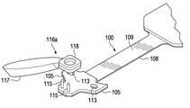
図1は、本開示技術の例示的な実施形態によるプローブ・チップと被試験デバイス(DUT)101との関係を示す分解上面斜視図である。図2は、図1のプローブ・チップ100の一部分の底面斜視図である。図1及び2に示すように、試験測定プローブ102用のプローブ・チップ100は、信号経路部104、取付タブ105及び接続ポイント107を含んでいても良い。DUT101は、例えば、DDR(double-data-rate)チップのような回路基板又は回路チップであっても良く、また、少なくとも1つの試験ポイント106を含んでもよい。試験ポイント106は、回路基板又は回路チップに接続されたインターポーザであるか、又は、こうしたインターポーザを含んでいても良い。試験測定用プローブ102は、オシロスコープなどの試験測定装置103に結合されても良い。 FIG. 1 is an exploded top perspective view showing the relationship between the probe chip and the device under test (DUT) 101 according to an exemplary embodiment of the disclosed technology. FIG. 2 is a bottom perspective view of a part of the
プローブ・チップ100の信号経路部104には、第1面(上面)108、第2面(下面)109、及び電気回路110が有る。電気回路110は、第1面108の一部、第2面109の一部、又はプローブ・チップ100の1つ以上の内部層(図示せず)の一部の任意の組合せとして組み込まれても良い。例えば、第1面108に組み込まれた回路110には、接続ポイント107からプローブ・チップ100上の他のアクティブ回路112(信号調整ICなど)への信号経路を提供するトレース111があっても良い。プローブ・チップ100の第2面109は、プローブ・チップ100の第1面108の裏側にある。図1及び図2に示すように、プローブ・チップ100の信号経路部104は、大まかに言って、参照番号104で示される構造体であるが、取付タブ105は除かれる。 The
取付タブ105には、後述のように、接着剤114(図3参照)が塗布されることがある。しかし、取付タブ105は、プローブ・チップ100の信号経路部104から遠ざかるように延びており、これにより、第1面108に組み込まれた回路110のトレース111は、接続ポイント107からプローブ・チップ100の信号経路部104に沿って延びることができる。プローブ・チップ100上の第1面108及びその他のアクティブ回路112に組み込まれた回路110の電気的挙動は、何らかの接着剤114が回路に誤って塗布された場合に悪影響を受ける可能性がある。このため、接続ポイント107及びトレース111から離して取付タブ105を配置することにより、接続ポイント107や、プローブ・チップ100上の第1面108又はその他のアクティブ回路112に組み込まれた回路110に接着剤114が塗布される危険が低くなる。 Adhesive 114 (see FIG. 3) may be applied to the mounting
この取付タブ105は、対象とする試験ポイント106の位置以外のDUT101上の位置において、DUT101に固定されるように構成されても良い。このような構成の例は、図3に関連して、以下で更に詳細に説明する。 The mounting
また、取付タブ105は、接着剤114を受けるよう構成された穴113を有していても良い。例えば、ユーザは、プローブ・チップ100の取付タブ105の穴113を通してDUT101に接着剤114を塗布しても良く、接着剤114が硬化すれば、プローブ・チップ100をDUT101に固定できる。接着剤114は、例えば、非導電性のUV硬化性接着剤であっても良く、このとき、UV硬化性接着剤とは、紫外線(UV)光に製剤を曝露することによって硬化する接着剤製剤である。穴113に関し、大まかに丸い穴やスロットとして図示しているが、他の形状も適しているであろう。UV硬化性接着剤と非導電性とするのは、この例では、取付タブ105の位置において、電気的接続を行わないためである。 Further, the mounting
変形例としては、プローブ・チップ100が、取付タブ105によって、DUT101に着脱可能に結合されても良い。この状況において、「着脱可能に結合」とは、プローブ・チップ100が、いずれのコンポーネントにも恒久的損傷を与えることなく、DUT101から分離及び移動できることを意味する。例えば、必要であれば、プローブ・チップ100をDUT101から取り外すことを可能にするために、接着剤114に熱を加えて軟化させても良い。 As a modification, the
図1及び2に示すように、接続ポイント107は、プローブ・チップ100の信号経路部104上に配置しても良い。接続ポイント107は、DUT101の所望の試験ポイント106と接触し、試験ポイント106をプローブ・チップ100の信号経路部104に組み込まれた回路110に(そして、実施形態によっては、最終的に、プローブ・チップ100上の他のアクティブ回路112に)電気的に接続するように構成されても良い。プローブ・チップ100の接続ポイント107は、更にピン又はワイヤ115を含んでいても良い。ピン115は、接続ポイント107をDUT101の試験ポイント106に結合するように構成されても良い。例えば、接続ポイント107のピン115は、DUT101の試験ポイント106に挿入されたり、直接接触して配置されたりしても良い。実施形態によっては、ピン115が、ばね仕掛け(spring-loaded)になっていても良い。上述したように、試験ポイント106は、回路基板又はチップに接続されたインターポーザであるか、又は、インターポーザを含んでいても良い。実施形態によっては、ピン115が、接続ポイント107を試験ポイント106に結合するように、接続ポイント107と試験ポイント106にはんだ付けされたワイヤであっても良い。実施形態によっては、ワイヤ115が、はんだではなく、導電性接着剤を使用して接続ポイント107と試験ポイント106との間に電気的に結合されても良い。好ましくは、ワイヤ115の長さは、試験ポイント106の目的の信号に対するワイヤ115の電気スタブ長の影響を最小限に抑えるために、できるだけ短く維持される。 As shown in FIGS. 1 and 2, the
いくつかの実施形態の例では、更に、脚部116があっても良く、これは、図1及び2に示す長く伸びた柄(ハンドル)117が付いた柄付き脚部116aのようなものか、又は、図1に示す長く伸びた柄のない脚部116bのようなものであっても良い。柄付きの脚部116aは、プローブ・チップ100の取付タブ105に結合されるとして図1及び2に示されており、一方、長く伸びた柄のない脚部116bは、柄付きの脚部116aの代替として図1に示されている。この脚部116は、DUT101の対象とする試験ポイント106の位置以外のDUT101上の位置において、DUT101に結合するように構成されても良い。例えば、脚部116には、基部118があっても良く、これにより、脚部116をDUT101に結合できる。この結合処理は、例えば、脚部116をUV硬化性接着剤のような接着剤114でDUT101に貼り付けても良い。変形例では、脚部116が、DUT101に着脱可能に結合される。この状況において、「着脱可能に結合」とは、いずれのコンポーネントにも恒久的な損傷を与えることなく、脚部116をDUT101から分離して取り外すことができることを意味する。例えば、必要であれば、脚部116をDUT101から取り外すために、接着剤に熱を加えてを軟化させても良い。柄付き脚部116aを有する実施形態例では、柄付き脚部116aに長く伸びた柄117があるために、DUT101からの柄付き脚部116aの取り外しが容易に行える。 In some embodiments, there may also be legs 116, such as the
この脚部116は、プローブ・チップ100の取付タブ105に結合するように構成されても良い。例えば、脚部116には、支柱部材119があっても良く、これは、プローブ・チップ100の取付タブ105の穴113に挿入される。いくつかの変形例では、支柱部材119を、プローブ・チップ100の取付タブ105の穴113に通して挿入すると、支柱部材119と取付タブ105の穴113との間の締まりばめ(interference fit)によって、取付タブ105の穴113に支柱部材119がカチッと留まる(スナップする)。例えば、取付タブ105の穴113は、脚部116の支柱部材119の溝型留め部に、ボタンとボタン・ホールの関係と同様に、カチッと留まる。いくつかの変形例では、支柱部材119を、プローブ・チップ100の取付タブ105の穴113に通して挿入するときに、キーロック機構を使用して取付タブ105を支柱部材119に機械的に固定しても良い。 The leg 116 may be configured to be coupled to the mounting
図3は、本願発明の実施形態のいくつかの例によるプローブ・チップ100の上面図であり、例示的なDUT101に対して配置されている。図3に示すように、いくつかのプローブ・チップ100では、DUT101の異なる試験ポイント106にアクセスして試験測定動作を行うために、比較的小さな領域に設置されても良い。本開示で使用される「試験測定動作」という用語は、DUT101から電気信号を取得するか、又は、DUT101に電気信号を注入することを意味する。 FIG. 3 is a top view of the
図3の例示的な第1実施形態120は、DUT101の試験ポイント106との接触して電気的接続を行うプローブ・チップ100の接続ポイント107を示し、プローブ・チップ100は、柄付き脚部116aによってDUT101に結合される。例示的な第2実施形態121及び例示的な第3実施形態122は、それぞれDUT101の試験ポイント106と接触して電気的に接続されるプローブ・チップ100の接続ポイント107を示し、プローブ・チップ100は、長く伸びた柄のない脚部116bによってDUT101に結合される。これら第2及び第3実施形態121及び122は、長く伸びた柄のない脚部116bを図示して説明しているが、これに代えて、いずれも柄付き脚部116aを用いても良い。いずれの場合でも、脚部116は、DUT101の対象とする試験ポイント106の位置以外のDUT101上の位置において、DUT101に結合されて良い。図示するように、脚部116は、プローブ・チップ100が接続されているDUT101の試験ポイント106の近くの面123に結合される。第3実施形態122の例に示すように、試験ポイント106の近くの面123は、回路基板又はチップ上の面123aであっても良い。 The exemplary
第1実施形態120、第2実施形態121及び第3実施形態122の夫々において、プローブ・チップ100を脚部116によってDUT101に結合する代わりに、又は、これに加えて、プローブ・チップ100の取付タブ105の穴113を通して又は穴113の周りに接着剤114を塗布することによって、プローブ・チップ100がDUT101に結合されても良い。次いで、接着剤114は、硬化するので、DUT101に対してプローブ・チップ100を、より強固に固定できる。説明したこれら実施形態の夫々において、粘着テープ124の貼付される範囲を、プローブ・チップ100の取付タブ105や脚部116を覆うほど長くしても良く、これにより、更なる安定性を提供できる。 In each of the
図3に示すように、これらの実施形態は、DUT101の対象とする試験ポイント106の位置以外のDUT101上の位置において、DUT101に貼付された、ある長さ(ある範囲)の粘着テープ124があっても良い。この粘着テープ124は、例えば、高粘着性(high-tack)の剥がして取り外し可能な粘着テープであっても良く、これは、発泡性の詰め物(foam padding)を含んでいない。このような実施形態では、粘着テープ124を貼付する範囲(長さ)を、DUT101と、取付タブ105又は脚部116の間として、プローブ・チップ100の取付タブ105又は脚部116が、粘着テープ124が存在する範囲で結合されても良い。このような実施形態では、必要に応じて、取付タブ105又は脚部116を、より容易にDUT101から取り外すことができるという利点がある。例えば、粘着テープ124の取付タブ105又は脚部116が結合されている範囲をDUT101から剥ぎ取ることができ、一旦、取り除けば、取付タブ105又は脚部116を(例えば、接着剤114に熱を加えて軟化させることによって)粘着テープ124から取り外すことができる。 As shown in FIG. 3, in these embodiments, there is an
図4は、本発明の実施形態によるプローブ・チップ100の分解上面斜視図であり、これには、プローブ・チップ100に結合可能なクリップ125がある。図5は、クリップ125が結合された状態の図4のプローブ・チップ100の分解上面斜視図である。これら実施形態では、プローブ・チップ100がDUT101に固定されたときに、クリップ125が、プローブ・チップ100とDUT101の間に存在していても良い。ある長さの粘着テープ124を用いる実施形態では、プローブ・チップ100が、粘着テープ124の貼付された部分によってDUT101に固定されたときに、クリップ125が、プローブ・チップ100と、粘着テープ124の貼付された部分との間に存在しても良い。 FIG. 4 is an exploded top perspective view of the
いくつかの実施形態では、クリップ125が、プローブ・チップ100に着脱可能に結合できる。この状況において、「着脱可能に結合」とは、クリップ125を、いずれのコンポーネントにも恒久的な損傷を与えることなく、プローブ・チップ100から分離して、取り外しできることを意味する。クリップ125には、例えば、取付タブ105の穴113に係合するように構成されたクリップ・ピン126があっても良い。クリップ・ピン126に加えて、又は、これの代わりに、クリップ125が、UV硬化性接着剤などの接着剤114でプローブ・チップ100に取付られても良い。必要に応じて、接着剤114に熱を加えて軟化させることで、プローブ・チップ100からクリップ125を取り外しできる。いくつかの実施形態において、クリップ125が、実質的に透明又は半透明であり、更に、非導電性のUV硬化性接着剤を硬化させる処理が、クリップ125を通してUV光を照射する処理を含む。本願で使用されるように、「実質的に透明又は半透明」とは、大部分の光が通過する又は本質的に光が通過することが可能なことを意味する。いくつかの実施形態では、クリップ125が、接着剤を使用せずに、プローブ・チップ100に着脱可能に結合され、これによって、クリップ125をプローブ・チップ100から容易に取り外しできる。いくつかの実施形態では、クリップ125とプローブ・チップ100がスナップ式で嵌合する(snap fit:カチッと嵌合する)ことで、クリップ125がプローブ・チップ100に着脱可能に結合される。 In some embodiments, the
クリップ125は、脚部116を使わずに、プローブ・チップ100をDUT101に結合する実施形態において、特に有益な場合がある。このような実施形態では、接着剤114を使って、プローブ・チップ100をDUT101に直接結合する代わりに、プローブ・チップ100とクリップ125の間に接着剤114を使用するか又は使用せずに、上述のように、プローブ・チップ100をクリップ125に結合しても良く、一方で、クリップ125は、接着剤114を使用してDUT101に結合しても良い。 The
図6は、プローブ・チップ100を被試験デバイスに固定する第1の例を示す。図6に示すように、プローブ・チップ100を被試験デバイス(DUT)101に固定する方法600では、ステップ602において、DUT101の試験ポイント106の近くにプローブ・チップ100を配置する。プローブ・チップ100には、その信号経路部104上の接続ポイント107と、取付タブ105とがある。接続ポイント107は、ステップ602において、DUT101の試験ポイント106と電気的に接続されても良い。取付タブ105は、プローブ・チップ100の信号経路部104から遠ざかるように伸びている。ステップ603では、プローブ・チップ100の取付タブ105の穴113を通して、DUT101に接着剤114を塗布する。そして、ステップ604では、接着剤114を硬化させて、プローブ・チップ100をDUT101に固定する。 FIG. 6 shows a first example of fixing the
実施形態によっては、ステップ603において、取付タブ105に接着剤114を塗布する処理に、プローブ・チップ100の取付タブ105に非導電性のUV硬化性接着剤を塗布する処理が含まれても良い。 Depending on the embodiment, in
実施形態によっては、ステップ602において、プローブ・チップ100を配置する処理が、プローブ・チップ100の接続ポイント107と試験ポイント106との間に、ピン又はワイヤ115を結合する処理を更に有していても良い。 In some embodiments, in
いくつかの実施形態において、方法600が、対象となる試験ポイント106の位置以外のDUT101上の位置において、DUT101に脚部116を固定する処理を更に有していても良い(ステップ601)。このような実施形態では、ステップ602において、DUT101の試験ポイント106の近くにプローブ・チップ100を配置する処理が、脚部116の支柱部材119をプローブ・チップ100の取付タブ105の穴113に通して挿入する処理を更に含んでもよい。実施形態によっては、支柱部材119を穴113に通して挿入する処理が、取付タブ105の穴113と支柱部材119との間の締まりばめ(interference fit)によって、取付タブ105の穴113に支柱部材119をカチッと留める(スナップする)処理を含んでもよい。実施形態によっては、脚部116の支柱部材119を穴113に通して挿入する処理において、キーロック機構を使用して取付タブ105を支柱部材119に機械的に固定しても良い。実施形態によっては、ステップ601において、脚部116をDUT101に固定する処理が、脚部116をDUT101に着脱可能に結合することを含む。実施形態によっては、脚部116(特に支柱部材119と基部118)が実質的に透明又は半透明であり、そして、ステップ601において、脚部116をDUT101に固定する処理が、非導電性のUV硬化性接着剤を脚部116(のDUT101と接着しようとする部分)に塗布する処理と、脚部116を通してUV光を照射することによって、このUV硬化性接着剤を硬化して脚部116をDUT101に固定する処理とを有していても良い。 In some embodiments, the
いくつかの実施形態において、方法600が、更に、DUT101の試験ポイント106について試験測定動作を行う処理(ステップ605)と、接着剤114に熱を加えて接着剤114を軟化させる処理(ステップ606)と、DUT101の試験ポイント106からプローブ・チップ100を取り外す処理(ステップ607)とを有していても良い。 In some embodiments, the
図7は、プローブ・チップ100を被試験デバイスに固定する第2の例を示す。図7に示すように、プローブ・チップ100を被試験デバイス(DUT)101に固定する方法700は、対象となる試験ポイント106の位置以外のDUT101上の位置において、DUT101に脚部116を固定する処理(ステップ701)と、DUT101の試験ポイント106の近くにプローブ・チップ100を配置する処理(ステップ702)とを有していても良い。プローブ・チップ100には、その信号経路部104上の接続ポイント107と、取付タブ105とがある。接続ポイント107は、ステップ702において、DUT101の試験ポイント106と電気的に接続されても良い。取付タブ105は、プローブ・チップ100の信号経路部104から遠ざかるように伸びており、支柱部材119と結合できる構造を有している。方法700には、更に、脚部116の支柱部材119を、プローブ・チップ100の取付タブ105の穴113に通して挿入する処理(ステップ703)があっても良い。 FIG. 7 shows a second example of fixing the
いくつかの実施形態では、方法700が、更に、支柱部材119と、プローブ・チップ100の取付タブ105に接着剤114を塗布する処理(ステップ704)を更に有していても良い。このような実施形態では、方法700が、更に、接着剤114を硬化させて、取付タブ105を支柱部材119に固定する処理(ステップ705)を有していても良い。 In some embodiments, the
いくつかの実施形態では、支柱部材119と取付タブ105に接着剤114を塗布する処理(ステップ704)が、支柱部材119とプローブ・チップ100の取付タブ105に非導電性のUV硬化性接着剤を塗布する処理を含んでも良い。 In some embodiments, the process of applying the adhesive 114 to the
いくつかの実施形態では、プローブ・チップ100を試験ポイント106の近くに配置する処理(ステップ702)が、プローブ・チップ100の接続ポイント107にあるピン115を試験ポイント106に結合する処理を更に有していても良い。 In some embodiments, the process of placing the
いくつかの実施形態では、ステップ703において、支柱部材119を取付タブ105の穴113に通して挿入する処理が、支柱部材119と取付タブ105の穴113との間の締まりばめ(interference fit)によって、支柱部材119を取付タブ105にカチッと留める(スナップする)処理を有していても良い。支柱部材119の穴113と係合する部分には、係合用の溝があっても良い。いくつかの実施形態では、ステップ703において、支柱部材119を穴113に通して挿入する処理が、キーロック機構を使用して取付タブ105を支柱部材119に機械的に固定する処理を有していても良い。 In some embodiments, in
いくつかの実施形態では、ステップ701において、脚部116をDUT101に結合する処理が、脚部116をDUT101に着脱可能に結合する処理を含む。 In some embodiments, in
いくつかの実施形態では、方法700が、DUT101の試験ポイント106について試験測定動作を行う処理(ステップ706)と、接着剤114に熱を加えて接着剤114を軟化させる処理(ステップ707)と、DUT101の試験ポイント106からプローブ・チップ100を取り外す処理(ステップ708)とを有していても良い。 In some embodiments, the
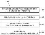
図8は、プローブ・チップ100を被試験デバイスに固定する第3の例を示す。図8に示すように、プローブ・チップ100を被試験デバイス(DUT)101に固定する方法800は、DUT101上の対象とする試験ポイント106の位置以外の場所に、ある長さの粘着テープ124を貼付する処理(ステップ801)と、DUT101の試験ポイント106の近くにプローブ・チップ100を配置する処理(ステップ802)とを有していても良い。プローブ・チップ100には、ステップ802において、DUT101の試験ポイント106と電気的に接続される接続ポイント107がある。方法800は、更に、粘着テープ124の貼付された範囲とプローブ・チップ100との間に接着剤114を塗布する処理(ステップ803)と、接着剤114を硬化させ、プローブ・チップ100を粘着テープ124の貼付された範囲に固定する処理(ステップ804)とを有していても良い。 FIG. 8 shows a third example of fixing the
いくつかの実施形態では、プローブ・チップ100が、プローブ・チップ100の信号経路部104の主要部に結合されるクリップ125を更に有していても良い。このような実施形態では、接着剤114を塗布する処理(ステップ803)が、粘着テープ124の貼付された範囲とプローブ・チップ100のクリップ125との間に接着剤114を塗布する処理を有していても良い。いくつかの実施形態では、接着剤114を塗布する処理(ステップ803)が、粘着テープ124の貼付された範囲とプローブ・チップ100のクリップ125との間に非導電性のUV硬化性接着剤を塗布する処理を有していても良い。このとき、クリップ125は、実質的に透明又は半透明であっても良く、クリップを通してUV光を照射することによって非導電性のUV硬化性接着剤を硬化させても良い。 In some embodiments, the
いくつかの実施形態では、プローブ・チップ100を配置する処理(ステップ802)が、プローブ・チップ100の接続ポイント107と試験ポイント106との間にピン115を結合する処理を更に有していても良い。 In some embodiments, even if the process of arranging the probe tip 100 (step 802) further comprises a process of coupling the
このように、開示された技術の様々実施形態は、DUTにプローブ・チップを固定するための改良された方法を提供する。
実施例As such, various embodiments of the disclosed technique provide an improved method for immobilizing a probe chip in a DUT.
Example
以下では、本願で開示される技術の理解に有益な実施例が提示される。この技術の実施形態は、以下で記述する実施例の1つ以上及び任意の組み合わせを含んでいても良い。 In the following, examples useful for understanding the techniques disclosed in the present application are presented. Embodiments of this technique may include one or more of the embodiments described below and any combination.
実施例1は、被試験デバイス(DUT)にプローブ・チップを固定する方法であって、
上記プローブ・チップは、該プローブ・チップの信号経路部上にある接続ポイントと、上記信号経路部から遠ざかるように伸びる取付タブとを有し、
上記方法は、
上記接続ポイントを上記DUTの試験ポイントと電気的に接続するように、上記DUTの上記試験ポイントの近くに上記プローブ・チップを配置する処理と、
上記プローブ・チップの上記取付タブの穴を通して上記DUTに接着剤を塗布する処理と、
上記接着剤を硬化させて上記DUTに上記プローブ・チップを固定する処理と
を具えている。The first embodiment is a method of fixing a probe chip to a device under test (DUT).
The probe chip has a connection point on the signal path portion of the probe chip and a mounting tab extending away from the signal path portion.
The above method
The process of arranging the probe chip near the test point of the DUT so that the connection point is electrically connected to the test point of the DUT.
The process of applying the adhesive to the DUT through the hole in the mounting tab of the probe tip, and
It is provided with a process of curing the adhesive and fixing the probe tip to the DUT.
実施例2は、実施例1の方法であって、プローブ・チップの取付タブに接着剤を塗布する処理が、上記プローブ・チップの上記取付タブにUV硬化性接着剤を塗布する処理を含む。 The second embodiment is the method of the first embodiment, and the process of applying the adhesive to the mounting tab of the probe tip includes the process of applying the UV curable adhesive to the mounting tab of the probe tip.
実施例3は、実施例1から2のいずれかの方法であって、DUTの試験ポイントの近くにプローブ・チップを配置する処理が、プローブ・チップの接続ポイントと試験ポイントとの間にピンを結合する処理を更に含む。 Example 3 is any of the methods 1 and 2, wherein the process of arranging the probe chip near the test point of the DUT puts a pin between the connection point of the probe chip and the test point. Further includes a process of combining.
実施例4は、実施例1から3のいずれの方法であって、脚部をDUTに固定する処理を更に具え、DUTの試験ポイントの近くにプローブ・チップを配置する処理が、脚部の支柱部材をプローブ・チップの取付タブの穴に通して挿入する処理を更に含む。 The fourth embodiment is any of the methods 1 to 3, further comprising a process of fixing the leg to the DUT, and a process of arranging the probe tip near the test point of the DUT is a support of the leg. It further includes the process of inserting the member through the hole in the mounting tab of the probe tip.
実施例5は、実施例4の方法であって、脚部の支柱部材をプローブ・チップの取付タブの穴に通して挿入する処理が、脚部の支柱部材と取付タブの穴との間の締まりばめ(interference fit)によって、取付タブの穴に支柱部材をカチッと留める(スナップする)処理を含む。 The fifth embodiment is the method of the fourth embodiment, in which the process of inserting the leg member through the hole of the mounting tab of the probe tip is performed between the leg member and the hole of the mounting tab. Includes the process of snapping the strut member into the hole in the mounting tab by an interference fit.
実施例6は、実施例4又は5の方法であって、脚部の支柱部材をプローブ・チップの取付タブの穴に通して挿入する処理が、キーロック機構を使用して取付タブを支柱部材に機械的に固定する処理を含む。 The sixth embodiment is the method of the fourth or fifth embodiment, in which the process of inserting the strut member of the leg through the hole of the mounting tab of the probe tip uses the key lock mechanism to insert the strut member of the leg portion into the strut member. Includes the process of mechanically fixing to.
実施例7は、実施例4から6のいずれの方法であって、脚部をDUTに固定する処理が、脚部をDUTに着脱可能に固定する処理を含む。 Example 7 is any of the methods 4 to 6, wherein the process of fixing the leg to the DUT includes a process of detachably fixing the leg to the DUT.
実施例8は、実施例4から7のいずれの方法であって、脚部が実質的に透明又は半透明であり、脚部をDUTに固定する処理が、脚部に非導電性のUV硬化性の接着剤を塗布する処理と、脚部を通してUV光を照射することによって上記接着剤を硬化させて脚部をDUTに固定する処理と有する。 In Example 8, in any of the methods of Examples 4 to 7, the legs are substantially transparent or translucent, and the treatment of fixing the legs to the DUT is UV curing of the legs non-conductive. It has a process of applying a sex adhesive and a process of curing the adhesive by irradiating UV light through the legs to fix the legs to the DUT.
実施例9は、実施例1から8のいずれかの方法であって、DUTの試験ポイントについて試験測定動作を行う処理と、接着剤に熱を加えて接着剤を柔らかくする処理と、DUTの試験ポイントからプローブ・チップを取り外す処理とを更に具えている。なお、脚部をDUTに固定する実施例では、脚部に柄(ハンドル)が付いていても良い。 Example 9 is any of the methods 1 to 8, wherein a test measurement operation is performed on the test point of the DUT, a process of applying heat to the adhesive to soften the adhesive, and a DUT test. It also includes a process to remove the probe tip from the point. In the embodiment in which the leg portion is fixed to the DUT, the leg portion may have a handle.
実施例10は、被試験デバイス(DUT)にプローブ・チップを固定する方法であって、
上記プローブ・チップは、該プローブ・チップの信号経路部上にある接続ポイントと、上記信号経路部から遠ざかるように伸びる取付タブとを有し、
上記方法は、
脚部を上記DUTに固定する処理と、
上記接続ポイントを上記DUTの試験ポイントと電気的に接続するように、上記DUTの上記試験ポイントの近くに上記プローブ・チップを配置する処理と、
上記脚部の支柱部材をプローブ・チップの取付タブの穴に通して挿入する処理と
を具えている。Example 10 is a method of fixing the probe chip to the device under test (DUT).
The probe chip has a connection point on the signal path portion of the probe chip and a mounting tab extending away from the signal path portion.
The above method
The process of fixing the legs to the above DUT and
The process of arranging the probe chip near the test point of the DUT so that the connection point is electrically connected to the test point of the DUT.
It is provided with a process of inserting the support column member of the leg through the hole of the mounting tab of the probe tip.
実施例11は、実施例10の方法であって、脚部の支柱部材とプローブ・チップの取付タブに接着剤を塗布する処理を更に具えている。 The eleventh embodiment is the method of the tenth embodiment, further comprising a process of applying an adhesive to the support column member of the leg and the mounting tab of the probe tip.
実施例12は、実施例11の方法であって、脚部の支柱部材とプローブ・チップの取付タブに接着剤を塗布する処理が、脚部の支柱部材とプローブ・チップの取付タブにUV硬化性の接着剤を塗布する処理を含む。 The twelfth embodiment is the method of the eleventh embodiment, in which the process of applying the adhesive to the strut member of the leg and the mounting tab of the probe tip is UV-cured to the strut member of the leg and the mounting tab of the probe tip. Includes the process of applying a sex adhesive.
実施例13は、実施例11又は12の方法であって、接着剤を硬化させて取付タブを支柱部材に固定する処理を更に具えている。 The thirteenth embodiment is the method of the eleventh or twelfth embodiment, further comprising a process of curing the adhesive to fix the mounting tab to the strut member.
実施例14は、実施例10から13のいずれの方法であって、DUTの試験ポイントの近くにプローブ・チップを配置する処理が、プローブ・チップの接続ポイントと試験ポイントとの間にピンを結合する処理を更に有する。 In Example 14, any method of Examples 10 to 13, in which the process of arranging the probe chip near the test point of the DUT connects a pin between the connection point of the probe chip and the test point. Further has a processing to be performed.
実施例15は、実施例10から14のいずれの方法であって、脚部の支柱部材をプローブ・チップの取付タブの穴に通して挿入する処理が、脚部の支柱部材と取付タブの穴との間の締まりばめ(interference fit)によって、取付タブの穴に支柱部材をカチッと留める(スナップする)処理を含む。 In the fifteenth embodiment, in any of the methods 10 to 14, the process of inserting the strut member of the leg through the hole of the mounting tab of the probe tip is the process of inserting the strut member of the leg through the hole of the strut member of the leg and the mounting tab. Includes the process of snapping the strut member into the hole in the mounting tab by an interference fit between and.
実施例16は、実施例10から15のいずれの方法であって、脚部の支柱部材をプローブ・チップの取付タブの穴に通して挿入する処理が、キーロック機構を使用して取付タブを支柱部材に機械的に固定する処理を含む。 In the 16th embodiment, in any of the methods 10 to 15, the process of inserting the support column member of the leg through the hole of the mounting tab of the probe tip is performed by using the key lock mechanism to insert the mounting tab. Includes processing to mechanically fix to the strut member.
実施例17は、実施例10から16のいずれの方法であって、脚部をDUTに固定する処理が、脚部をDUTに着脱可能に固定する処理を含む。 Example 17 is any of the methods 10 to 16, wherein the process of fixing the leg to the DUT includes a process of detachably fixing the leg to the DUT.
実施例18は、実施例10から17のいずれの方法であって、DUTの試験ポイントについて試験測定動作を行う処理と、接着剤に熱を加えて接着剤を柔らかくする処理と、DUTの試験ポイントからプローブ・チップを取り外す処理とを更に具えている。なお、脚部をDUTに固定する実施例では、脚部に柄(ハンドル)が付いていても良い。 Example 18 is any of the methods of Examples 10 to 17, a process of performing a test measurement operation on a DUT test point, a process of applying heat to the adhesive to soften the adhesive, and a DUT test point. It also has a process to remove the probe chip from. In the embodiment in which the leg portion is fixed to the DUT, the leg portion may have a handle.
実施例19は、被試験デバイス(DUT)にプローブ・チップを固定する方法であって、
ある長さの粘着テープをDUTに貼付する処理と、
上記プローブ・チップの接続ポイントを上記DUTの試験ポイントと電気的に接続するように、上記DUTの上記試験ポイントの近くに上記プローブ・チップを配置する処理と、
上記粘着テープの貼付された部分と上記プローブ・チップとの間に接着剤を塗布する処理と、
上記接着剤を硬化させて上記プローブ・チップを上記粘着テープの貼付された部分に固定する処理と
を具えている。Example 19 is a method of fixing the probe chip to the device under test (DUT).
The process of attaching an adhesive tape of a certain length to the DUT,
The process of arranging the probe chip near the test point of the DUT so that the connection point of the probe chip is electrically connected to the test point of the DUT.
The process of applying an adhesive between the part where the adhesive tape is attached and the probe tip,
It includes a process of curing the adhesive and fixing the probe tip to the portion to which the adhesive tape is attached.
実施例20は、実施例19の方法であって、プローブ・チップが、プローブ・チップに結合されたクリップを更に有し、上記粘着テープの貼付された部分と上記プローブ・チップとの間に接着剤を塗布する処理が、上記粘着テープの貼付された部分と上記プローブ・チップの上記クリップとの間に接着剤を塗布する処理を有する。 Example 20 is the method of Example 19, wherein the probe tip further has a clip attached to the probe tip and is adhered between the portion to which the adhesive tape is attached and the probe tip. The process of applying the agent includes a process of applying an adhesive between the portion to which the adhesive tape is attached and the clip of the probe tip.
実施例21は、実施例20の方法であって、上記クリップは、実質的に透明又は半透明であり、上記粘着テープの貼付された部分と上記クリップとの間に接着剤を塗布する処理が、上記粘着テープの貼付された部分と上記クリップとの間に非導電性のUV硬化性接着剤を塗布する処理を有し、上記プローブ・チップを上記粘着テープの貼付された部分に固定する処理が、上記クリップを通してUV光を照射することによって上記非導電性のUV硬化性接着剤を硬化させる処理を含む。 Example 21 is the method of Example 20, in which the clip is substantially transparent or translucent, and a treatment of applying an adhesive between the portion to which the adhesive tape is attached and the clip is performed. , A process of applying a non-conductive UV curable adhesive between the portion to which the adhesive tape is attached and the clip, and a process of fixing the probe tip to the portion to which the adhesive tape is attached. However, it comprises a process of curing the non-conductive UV curable adhesive by irradiating the UV light through the clip.
実施例22は、実施例19から21のいずれの方法であって、上記DUTの上記試験ポイントの近くに上記プローブ・チップを配置する処理が、プローブ・チップの接続ポイントと試験ポイントとの間にピンを結合する処理を更に含む。 In Example 22, in any of the methods 19 to 21, the process of arranging the probe chip near the test point of the DUT is performed between the connection point of the probe chip and the test point. It further includes a process of joining pins.
実施例23には、実施例19から22のいずれの方法であって、DUTの試験ポイントについて試験測定動作を行う処理と、粘着テープの貼付された部分をDUTから剥がす処理と、接着剤に熱を加えて接着剤を柔らかくする処理と、粘着テープからプローブ・チップを取り外す処理とを更に具えている。 In Example 23, in any of the methods 19 to 22, a process of performing a test measurement operation on the test point of the DUT, a process of peeling the portion to which the adhesive tape is attached from the DUT, and a heat of the adhesive are applied. The process of adding the adhesive to soften the adhesive and the process of removing the probe tip from the adhesive tape are further provided.
実施例24は、試験測定プローブ用のプローブ・チップであって、
少なくとも1つの信号経路を有する信号経路部と、
被試験デバイス上の試験ポイントを少なくとも1つの上記信号経路に電気的に接続するよう構成される上記信号経路上の接続ポイントと、
上記信号経路部から遠ざかるように伸びる取付タブと
を具え、
上記取付タブは、接着剤で接着するための面を提供するように構成される。Example 24 is a probe chip for a test measurement probe.
A signal path section having at least one signal path,
A connection point on the signal path configured to electrically connect the test point on the device under test to at least one of the signal paths.
Equipped with a mounting tab that extends away from the above signal path,
The mounting tabs are configured to provide a surface for adhering with an adhesive.
実施例25は、実施例24のプローブ・チップであって、上記取付タブは、DUTに固定された脚部の支柱部材を受けるように構成された穴を有する。 The 25th embodiment is the probe tip of the 24th embodiment, and the mounting tab has a hole configured to receive a strut member of a leg fixed to the DUT.
本開示技術の態様は、特別に作成されたハードウェア、ファームウェア、デジタル・シグナル・プロセッサ又はプログラムされた命令に従って動作するプロセッサを含む特別にプログラムされた汎用コンピュータ上で動作できる。本願における「コントローラ」又は「プロセッサ」という用語は、マイクロプロセッサ、マイクロコンピュータ、ASIC及び専用ハードウェア・コントローラ等を意図する。本開示技術の態様は、1つ又は複数のコンピュータ(モニタリング・モジュールを含む)その他のデバイスによって実行される、1つ又は複数のプログラム・モジュールなどのコンピュータ利用可能なデータ及びコンピュータ実行可能な命令で実現できる。概して、プログラム・モジュールとしては、ルーチン、プログラム、オブジェクト、コンポーネント、データ構造などを含み、これらは、コンピュータその他のデバイス内のプロセッサによって実行されると、特定のタスクを実行するか、又は、特定の抽象データ形式を実現する。コンピュータ実行可能命令は、ハードディスク、光ディスク、リムーバブル記憶媒体、ソリッド・ステート・メモリ、RAMなどのコンピュータ可読記憶媒体に記憶しても良い。当業者には理解されるように、プログラム・モジュールの機能は、様々な実施例において必要に応じて組み合わせられるか又は分散されても良い。更に、こうした機能は、集積回路、フィールド・プログラマブル・ゲート・アレイ(FPGA)などのようなファームウェア又はハードウェア同等物において全体又は一部を具体化できる。特定のデータ構造を使用して、本開示技術の1つ以上の態様をより効果的に実施することができ、そのようなデータ構造は、本願に記載されたコンピュータ実行可能命令及びコンピュータ使用可能データの範囲内と考えられる。 Aspects of the present disclosure can operate on specially programmed general purpose computers including specially crafted hardware, firmware, digital signal processors or processors operating according to programmed instructions. The term "controller" or "processor" in the present application is intended for microprocessors, microcomputers, ASICs, dedicated hardware controllers, and the like. Aspects of the present disclosure are computer-available data such as one or more program modules and computer-executable instructions executed by one or more computers (including monitoring modules) and other devices. realizable. In general, program modules include routines, programs, objects, components, data structures, etc., which, when executed by a processor in a computer or other device, perform a particular task or perform a particular task. Realize an abstract data format. Computer-executable instructions may be stored on a computer-readable storage medium such as a hard disk, optical disk, removable storage medium, solid state memory, RAM, or the like. As will be appreciated by those skilled in the art, the functions of the program modules may be combined or distributed as needed in various embodiments. Moreover, these features can be embodied in whole or in part in firmware or hardware equivalents such as integrated circuits, field programmable gate arrays (FPGAs), etc. Certain data structures can be used to more effectively implement one or more aspects of the disclosed art, such data structures being computer executable instructions and computer usable data described herein. It is considered to be within the range of.
開示された主題の上述のバージョンは、記述したか又は当業者には明らかであろう多くの効果を有する。それでも、開示された装置、システム又は方法のすべてのバージョンにおいて、これらの効果又は特徴のすべてが要求されるわけではない。 The above-mentioned versions of the disclosed subject matter have many effects that have been described or will be apparent to those of skill in the art. Nevertheless, not all of these effects or features are required in all versions of the disclosed devices, systems or methods.
加えて、本願の記述は、特定の特徴に言及している。本明細書における開示には、これらの特定の特徴の全ての可能な組み合わせが含まれると理解すべきである。ある特定の特徴が特定の態様又は実施例の状況において開示される場合、その特徴は、可能である限り、他の態様及び実施例の状況においても利用できる。 In addition, the description of this application refers to specific features. It should be understood that the disclosure herein includes all possible combinations of these particular features. If a particular feature is disclosed in a particular aspect or context of an embodiment, the feature may also be used in the context of other embodiments and examples where possible.
また、本願において、2つ以上の定義されたステップ又は工程を有する方法に言及する場合、これら定義されたステップ又は工程は、状況的にそれらの可能性を排除しない限り、任意の順序で又は同時に実行しても良い。 Also, when referring to a method having two or more defined steps or steps in the present application, these defined steps or steps may be in any order or simultaneously, unless the circumstances rule out their possibility. You may do it.
更に、用語「を具える(comprises)」及びその文法的に等価なものは、本願において、他のコンポーネント(components)、機能(features)、ステップ、処理(processes)、工程(operations)がオプションで存在することを示すのに使用される。例えば、コンポーネントA、B及びC「を具える(comprising)」又は「何かが」コンポーネントA、B及びC「を具える(which comprises)」という条件は、コンポーネントA、B及びCだけを含んでも良いし、又は、コンポーネントA、B及びCと共に1つ以上の他のコンポーネントを含んでいても良い。 In addition, the term "comprises" and its grammatical equivalents are optional in this application with other components, features, steps, processes, operations. Used to indicate that it exists. For example, the condition that "comprising" or "something" components A, B and C "comprising" includes only components A, B and C. It may be used, or it may include one or more other components together with the components A, B and C.
説明の都合上、本発明の具体的な実施例を図示し、説明してきたが、本発明の要旨と範囲から離れることなく、種々の変更が可能なことが理解できよう。 For convenience of explanation, specific embodiments of the present invention have been illustrated and described, but it can be understood that various changes can be made without departing from the gist and scope of the present invention.
100 プローブ・チップ
101 被試験デバイス(DUT)
102 試験測定プローブ
103 試験測定装置
104 信号経路部
105 取付タブ
106 試験ポイント
107 接続ポイント
108 第1面(上面)
109 第2面(下面)
110 電気回路
111 信号トレース
113 取付タブの穴
114 接着剤
115 ピン又はワイヤ
116 脚部
116a 長く伸びた柄付き脚部
116b 長く伸びた柄のない脚部
118 基部
119 支柱部材
120 第1実施形態例
121 第2実施形態例
122 第3実施形態例
124 粘着テープ
125 クリップ
126 クリップ・ピン100
102
109 Second surface (lower surface)
110
Claims (12)
Translated fromJapanese上記プローブ・チップは、該プローブ・チップの信号経路部上にある接続ポイントと、上記信号経路部から遠ざかるように伸びる取付タブとを有し、
上記方法は、
脚部を上記DUTに固定する処理と、
上記接続ポイントを上記DUTの試験ポイントと電気的に接続するように、上記DUTの上記試験ポイントの近くに上記プローブ・チップを配置する処理と、
上記脚部をプローブ・チップの取付タブの穴に通して挿入する処理と
を具えるプローブ・チップ固定方法。A method of fixing the probe chip to the device under test (DUT).
The probe chip has a connection point on the signal path portion of the probe chip and a mounting tab extending away from the signal path portion.
The above method
The process of fixing the legs to the above DUT and
The process of arranging the probe chip near the test point of the DUT so that the connection point is electrically connected to the test point of the DUT.
A probe tip fixing method that includes a process of inserting the above leg through the hole of the probe tip mounting tab.
上記プローブ・チップは、該プローブ・チップの信号経路部上にある接続ポイントと、上記信号経路部から遠ざかるように伸びる取付タブとを有し、
上記方法は、
上記接続ポイントを上記DUTの試験ポイントと電気的に接続するように、上記DUTの上記試験ポイントの近くに上記プローブ・チップを配置する処理と、
上記プローブ・チップの上記取付タブの穴を通して上記DUTに接着剤を塗布する処理と、
上記接着剤を硬化させて上記DUTに上記プローブ・チップを固定する処理と
を具えるプローブ・チップ固定方法。A method of fixing the probe chip to the device under test (DUT).
The probe chip has a connection point on the signal path portion of the probe chip and a mounting tab extending away from the signal path portion.
The above method
The process of arranging the probe chip near the test point of the DUT so that the connection point is electrically connected to the test point of the DUT.
The process of applying the adhesive to the DUT through the hole in the mounting tab of the probe tip, and
A probe / tip fixing method including a process of curing the adhesive and fixing the probe / tip to the DUT.
上記接着剤に熱を加えて上記接着剤を軟化させる処理と、
上記DUTの上記試験ポイントから上記プローブ・チップを取り外す処理と
を更に具える請求項1から4のいずれかのプローブ・チップ固定方法。Processing to perform test measurement operation for the above test points of the above DUT, and
The process of applying heat to the adhesive to soften the adhesive,
The probe chip fixing method according to any one of claims 1 to 4, further comprising a process of removing the probe chip from the test point of the DUT.
上記脚部をDUTに固定する処理が、上記脚部に非導電性のUV硬化性接着剤を塗布する処理と、上記脚部を通してUV光を照射することによって上記UV硬化性接着剤を硬化させて上記脚部を上記DUTに固定する処理と有する請求項1から3のいずれかのプローブ・チップ固定方法。The legs are substantially transparent or translucent and
The process of fixing the legs to the DUT is a process of applying a non-conductive UV curable adhesive to the legs and a process of irradiating UV light through the legs to cure the UV curable adhesive. The probe / tip fixing method according to any one of claims 1 to 3, further comprising a process of fixing the leg portion to the DUT.
ある長さの粘着テープをDUTに貼付する処理と、
上記プローブ・チップの接続ポイントを上記DUTの試験ポイントと電気的に接続するように、上記DUTの上記試験ポイントの近くに上記プローブ・チップを配置する処理と、
上記粘着テープの貼付された部分と上記プローブ・チップとの間に接着剤を塗布する処理と、
上記接着剤を硬化させて上記プローブ・チップを上記粘着テープの貼付された部分に固定する処理と
を具えるプローブ・チップ固定方法。A method of fixing the probe chip to the device under test (DUT).
The process of attaching an adhesive tape of a certain length to the DUT,
The process of arranging the probe chip near the test point of the DUT so that the connection point of the probe chip is electrically connected to the test point of the DUT.
The process of applying an adhesive between the part where the adhesive tape is attached and the probe tip,
A probe / tip fixing method including a process of curing the adhesive and fixing the probe / tip to the portion to which the adhesive tape is attached.
上記粘着テープの貼付された部分を上記DUTから剥がす処理と、
上記接着剤に熱を加えて上記接着剤を軟化させる処理と、
上記粘着テープから上記プローブ・チップを取り外す処理と
を更に具える請求項8から10のいずれかのプローブ・チップ固定方法。Processing to perform test measurement operation for the above test points of the above DUT, and
The process of peeling off the part to which the adhesive tape is attached from the DUT, and
The process of applying heat to the adhesive to soften the adhesive,
The probe chip fixing method according to any one of claims 8 to 10, further comprising a process of removing the probe chip from the adhesive tape.
少なくとも1つの信号経路を有する信号経路部と、
被試験デバイス上の試験ポイントを少なくとも1つの上記信号経路に電気的に接続するよう構成される上記信号経路上の接続ポイントと、
上記信号経路部から遠ざかるように伸びる取付タブと
を具え、
上記取付タブは、接着剤で接着するための面を提供するように構成されるプローブ・チップ。A probe tip for test and measurement probes
A signal path section having at least one signal path,
A connection point on the signal path configured to electrically connect the test point on the device under test to at least one of the signal paths.
Equipped with a mounting tab that extends away from the above signal path,
The mounting tab is a probe tip configured to provide a surface for gluing.
Applications Claiming Priority (4)
| Application Number | Priority Date | Filing Date | Title |
|---|---|---|---|
| US202063049548P | 2020-07-08 | 2020-07-08 | |
| US63/049,548 | 2020-07-08 | ||
| US17/339,877 | 2021-06-04 | ||
| US17/339,877US12055578B2 (en) | 2020-07-08 | 2021-06-04 | Securing a probe to a device under test |
Publications (1)
| Publication Number | Publication Date |
|---|---|
| JP2022016381Atrue JP2022016381A (en) | 2022-01-21 |
Family
ID=79020346
Family Applications (1)
| Application Number | Title | Priority Date | Filing Date |
|---|---|---|---|
| JP2021113369APendingJP2022016381A (en) | 2020-07-08 | 2021-07-08 | Probe tip and its fixing method |
Country Status (5)
| Country | Link |
|---|---|
| US (1) | US12055578B2 (en) |
| JP (1) | JP2022016381A (en) |
| CN (1) | CN113917194A (en) |
| DE (1) | DE102021117364A1 (en) |
| TW (1) | TW202202850A (en) |
Citations (10)
| Publication number | Priority date | Publication date | Assignee | Title |
|---|---|---|---|---|
| JPH0664212U (en)* | 1993-02-15 | 1994-09-09 | 日本航空電子工業株式会社 | Optical fiber coupler |
| JPH0846375A (en)* | 1994-07-28 | 1996-02-16 | Seiko Epson Corp | Miniature electronic apparatus |
| US20040201388A1 (en)* | 2003-04-08 | 2004-10-14 | Barr Andrew Harvey | Support for an electronic probe and related methods |
| US20070256511A1 (en)* | 2006-05-08 | 2007-11-08 | Stevens Kerry A | Probe holder for various thickness substrates |
| JP2008039768A (en)* | 2006-07-10 | 2008-02-21 | Tokyo Electron Ltd | Probe card |
| JP2010078596A (en)* | 2008-09-23 | 2010-04-08 | Tektronix Inc | Probe assembly |
| US8134377B1 (en)* | 2005-08-31 | 2012-03-13 | Lecroy Corporation | Adherable holder and locater tool |
| JP2014122905A (en)* | 2012-12-21 | 2014-07-03 | Tektronix Inc | High bandwidth solder-less lead and measurement system |
| CN105388336A (en)* | 2015-10-16 | 2016-03-09 | 昆山龙腾光电有限公司 | Auxiliary testing device for oscilloscope probes |
| JP2019002916A (en)* | 2017-05-26 | 2019-01-10 | テクトロニクス・インコーポレイテッドTektronix,Inc. | Test probe tip and method of bonding the test probe tip to a device under test |
Family Cites Families (5)
| Publication number | Priority date | Publication date | Assignee | Title |
|---|---|---|---|---|
| US4209742A (en)* | 1976-10-13 | 1980-06-24 | Tektronix, Inc. | Modular probe system |
| US7049843B2 (en)* | 2004-03-10 | 2006-05-23 | Tektronix, Inc. | Signal acquisition probing system using a micro-cavity laser capable of sensing DC voltages |
| US7056134B2 (en)* | 2004-05-27 | 2006-06-06 | Tektronix, Inc. | Attachable/detachable probing tip system for a measurement probing system |
| CN103575943B (en)* | 2012-07-31 | 2018-08-03 | 特克特朗尼克公司 | Signal acquisition probe detects end |
| CN107179428A (en)* | 2016-03-09 | 2017-09-19 | 中兴通讯股份有限公司 | Test oscilloprobe, method, the apparatus and system of ripple |
- 2021
- 2021-06-04USUS17/339,877patent/US12055578B2/enactiveActive
- 2021-06-16TWTW110121840Apatent/TW202202850A/enunknown
- 2021-07-05CNCN202110755963.2Apatent/CN113917194A/enactivePending
- 2021-07-06DEDE102021117364.7Apatent/DE102021117364A1/enactivePending
- 2021-07-08JPJP2021113369Apatent/JP2022016381A/enactivePending
Patent Citations (10)
| Publication number | Priority date | Publication date | Assignee | Title |
|---|---|---|---|---|
| JPH0664212U (en)* | 1993-02-15 | 1994-09-09 | 日本航空電子工業株式会社 | Optical fiber coupler |
| JPH0846375A (en)* | 1994-07-28 | 1996-02-16 | Seiko Epson Corp | Miniature electronic apparatus |
| US20040201388A1 (en)* | 2003-04-08 | 2004-10-14 | Barr Andrew Harvey | Support for an electronic probe and related methods |
| US8134377B1 (en)* | 2005-08-31 | 2012-03-13 | Lecroy Corporation | Adherable holder and locater tool |
| US20070256511A1 (en)* | 2006-05-08 | 2007-11-08 | Stevens Kerry A | Probe holder for various thickness substrates |
| JP2008039768A (en)* | 2006-07-10 | 2008-02-21 | Tokyo Electron Ltd | Probe card |
| JP2010078596A (en)* | 2008-09-23 | 2010-04-08 | Tektronix Inc | Probe assembly |
| JP2014122905A (en)* | 2012-12-21 | 2014-07-03 | Tektronix Inc | High bandwidth solder-less lead and measurement system |
| CN105388336A (en)* | 2015-10-16 | 2016-03-09 | 昆山龙腾光电有限公司 | Auxiliary testing device for oscilloscope probes |
| JP2019002916A (en)* | 2017-05-26 | 2019-01-10 | テクトロニクス・インコーポレイテッドTektronix,Inc. | Test probe tip and method of bonding the test probe tip to a device under test |
Also Published As
| Publication number | Publication date |
|---|---|
| DE102021117364A1 (en) | 2022-01-13 |
| TW202202850A (en) | 2022-01-16 |
| US12055578B2 (en) | 2024-08-06 |
| CN113917194A (en) | 2022-01-11 |
| US20220011361A1 (en) | 2022-01-13 |
Similar Documents
| Publication | Publication Date | Title |
|---|---|---|
| JP2010078596A (en) | Probe assembly | |
| TW201100811A (en) | Probe card | |
| CN106841986A (en) | PCBA board test device and system | |
| CN108929638B (en) | Component attachment technique using UV-cured conductive adhesive | |
| TWI472770B (en) | Probe card for testing film package | |
| JP6454467B2 (en) | High bandwidth solderless lead and measurement system | |
| US7091731B1 (en) | Flexible ribbon probe for peripheral leads of an electronic part's package | |
| JP2022016381A (en) | Probe tip and its fixing method | |
| TW595290B (en) | Electronic device having connection structure and connection method thereof | |
| JPH11287846A (en) | Test probe assembly | |
| US20200146194A1 (en) | Back-drilled via probing techniques | |
| US5175496A (en) | Dual contact beam assembly for an IC test fixture | |
| CN101726635A (en) | probe card | |
| CN108535552B (en) | Testing device | |
| TW526692B (en) | A method of repairing a printed circuit assembly on a printed circuit board by attaching a flexible circuit to said circuit board and flexible circuits for repair of a printed circuit assembly and for reparing defects in a circuit assembly | |
| EP2866037B1 (en) | Releaseable probe connection | |
| JP6630117B2 (en) | Contact unit and inspection jig | |
| JP2008286657A (en) | Probe card and electronic component testing device including the same | |
| US8278955B2 (en) | Test interconnect | |
| CN104215801B (en) | Probe card and manufacturing method thereof | |
| JP2737774B2 (en) | Wafer tester | |
| JP2009063469A (en) | Signal-drawing tool for surface mounted component | |
| JP3595305B2 (en) | Pre-mounting test probe | |
| CN114624568B (en) | Failure analysis device | |
| JP2007064841A (en) | Calibration board for electronic component tester |
Legal Events
| Date | Code | Title | Description |
|---|---|---|---|
| A521 | Request for written amendment filed | Free format text:JAPANESE INTERMEDIATE CODE: A821 Effective date:20220201 | |
| RD02 | Notification of acceptance of power of attorney | Free format text:JAPANESE INTERMEDIATE CODE: A7422 Effective date:20220201 | |
| A625 | Written request for application examination (by other person) | Free format text:JAPANESE INTERMEDIATE CODE: A625 Effective date:20240603 | |
| A131 | Notification of reasons for refusal | Free format text:JAPANESE INTERMEDIATE CODE: A131 Effective date:20250128 | |
| A601 | Written request for extension of time | Free format text:JAPANESE INTERMEDIATE CODE: A601 Effective date:20250428 | |
| A601 | Written request for extension of time | Free format text:JAPANESE INTERMEDIATE CODE: A601 Effective date:20250626 | |
| A521 | Request for written amendment filed | Free format text:JAPANESE INTERMEDIATE CODE: A523 Effective date:20250728 | |
| A01 | Written decision to grant a patent or to grant a registration (utility model) | Free format text:JAPANESE INTERMEDIATE CODE: A01 Effective date:20250909 |