JP2022003409A - Display divice - Google Patents
Display diviceDownload PDFInfo
- Publication number
- JP2022003409A JP2022003409AJP2021162495AJP2021162495AJP2022003409AJP 2022003409 AJP2022003409 AJP 2022003409AJP 2021162495 AJP2021162495 AJP 2021162495AJP 2021162495 AJP2021162495 AJP 2021162495AJP 2022003409 AJP2022003409 AJP 2022003409A
- Authority
- JP
- Japan
- Prior art keywords
- film
- substrate
- peeled
- adhesive
- metal
- Prior art date
- Legal status (The legal status is an assumption and is not a legal conclusion. Google has not performed a legal analysis and makes no representation as to the accuracy of the status listed.)
- Withdrawn
Links
- 239000000758substrateSubstances0.000claimsabstractdescription251
- 239000004065semiconductorSubstances0.000claimsabstractdescription71
- 229910044991metal oxideInorganic materials0.000claimsabstractdescription68
- 150000004706metal oxidesChemical class0.000claimsabstractdescription68
- 229910052710siliconInorganic materials0.000claimsabstractdescription19
- 239000010703siliconSubstances0.000claimsabstractdescription19
- XUIMIQQOPSSXEZ-UHFFFAOYSA-NSiliconChemical compound[Si]XUIMIQQOPSSXEZ-UHFFFAOYSA-N0.000claimsdescription18
- 239000012535impuritySubstances0.000claimsdescription14
- 238000007789sealingMethods0.000claimsdescription6
- 239000010408filmSubstances0.000abstractdescription327
- 229910052751metalInorganic materials0.000abstractdescription104
- 239000002184metalSubstances0.000abstractdescription104
- 239000000853adhesiveSubstances0.000abstractdescription94
- 230000001070adhesive effectEffects0.000abstractdescription94
- 238000000034methodMethods0.000abstractdescription40
- 230000001678irradiating effectEffects0.000abstractdescription21
- 238000012546transferMethods0.000abstractdescription18
- 230000008569processEffects0.000abstractdescription17
- 238000010586diagramMethods0.000abstractdescription16
- 239000010409thin filmSubstances0.000abstractdescription8
- 239000010410layerSubstances0.000description107
- 239000000463materialSubstances0.000description51
- 239000004973liquid crystal related substanceSubstances0.000description49
- 238000010438heat treatmentMethods0.000description48
- 229920005989resinPolymers0.000description41
- 239000011347resinSubstances0.000description41
- 238000004519manufacturing processMethods0.000description31
- 230000009975flexible effectEffects0.000description22
- IJGRMHOSHXDMSA-UHFFFAOYSA-NAtomic nitrogenChemical compoundN#NIJGRMHOSHXDMSA-UHFFFAOYSA-N0.000description18
- VYPSYNLAJGMNEJ-UHFFFAOYSA-Nsilicon dioxideInorganic materialsO=[Si]=OVYPSYNLAJGMNEJ-UHFFFAOYSA-N0.000description18
- 230000001681protective effectEffects0.000description16
- 239000000956alloySubstances0.000description14
- 229910045601alloyInorganic materials0.000description12
- 238000004140cleaningMethods0.000description12
- 230000007547defectEffects0.000description12
- 229910052814silicon oxideInorganic materials0.000description12
- 238000004544sputter depositionMethods0.000description12
- 239000011521glassSubstances0.000description11
- QVGXLLKOCUKJST-UHFFFAOYSA-Natomic oxygenChemical compound[O]QVGXLLKOCUKJST-UHFFFAOYSA-N0.000description10
- 239000001301oxygenSubstances0.000description10
- 229910052760oxygenInorganic materials0.000description10
- 230000006837decompressionEffects0.000description9
- 229910052757nitrogenInorganic materials0.000description9
- XLYOFNOQVPJJNP-UHFFFAOYSA-NwaterSubstancesOXLYOFNOQVPJJNP-UHFFFAOYSA-N0.000description9
- 229910052581Si3N4Inorganic materials0.000description8
- 230000015572biosynthetic processEffects0.000description8
- 230000006866deteriorationEffects0.000description8
- 239000010453quartzSubstances0.000description8
- HQVNEWCFYHHQES-UHFFFAOYSA-Nsilicon nitrideChemical compoundN12[Si]34N5[Si]62N3[Si]51N64HQVNEWCFYHHQES-UHFFFAOYSA-N0.000description8
- 125000006850spacer groupChemical group0.000description8
- 238000005530etchingMethods0.000description7
- 150000004767nitridesChemical class0.000description7
- 229910052721tungstenInorganic materials0.000description7
- XKRFYHLGVUSROY-UHFFFAOYSA-NArgonChemical compound[Ar]XKRFYHLGVUSROY-UHFFFAOYSA-N0.000description6
- 230000006750UV protectionEffects0.000description6
- 238000002425crystallisationMethods0.000description6
- 230000008025crystallizationEffects0.000description6
- 229910052750molybdenumInorganic materials0.000description6
- 239000011368organic materialSubstances0.000description6
- 229920001187thermosetting polymerPolymers0.000description6
- 238000006243chemical reactionMethods0.000description5
- 229910010272inorganic materialInorganic materials0.000description5
- 239000011147inorganic materialSubstances0.000description5
- 229910021420polycrystalline siliconInorganic materials0.000description5
- -1polytetrafluoroethylenePolymers0.000description5
- 229910004298SiO 2Inorganic materials0.000description4
- 239000000654additiveSubstances0.000description4
- 230000000996additive effectEffects0.000description4
- 239000013078crystalSubstances0.000description4
- 238000009792diffusion processMethods0.000description4
- 239000003822epoxy resinSubstances0.000description4
- 230000006870functionEffects0.000description4
- 239000007789gasSubstances0.000description4
- 150000002739metalsChemical class0.000description4
- 239000000203mixtureSubstances0.000description4
- 150000002894organic compoundsChemical class0.000description4
- 238000005498polishingMethods0.000description4
- 229920000647polyepoxidePolymers0.000description4
- 229920006267polyester filmPolymers0.000description4
- 229920005591polysiliconPolymers0.000description4
- 239000002356single layerSubstances0.000description4
- 238000004528spin coatingMethods0.000description4
- 239000000126substanceSubstances0.000description4
- ZNOKGRXACCSDPY-UHFFFAOYSA-Ntungsten trioxideChemical compoundO=[W](=O)=OZNOKGRXACCSDPY-UHFFFAOYSA-N0.000description4
- MYMOFIZGZYHOMD-UHFFFAOYSA-NDioxygenChemical compoundO=OMYMOFIZGZYHOMD-UHFFFAOYSA-N0.000description3
- NIXOWILDQLNWCW-UHFFFAOYSA-Nacrylic acid groupChemical groupC(C=C)(=O)ONIXOWILDQLNWCW-UHFFFAOYSA-N0.000description3
- 229910052786argonInorganic materials0.000description3
- 239000000919ceramicSubstances0.000description3
- 229910001882dioxygenInorganic materials0.000description3
- 238000005516engineering processMethods0.000description3
- 239000011159matrix materialSubstances0.000description3
- 239000002985plastic filmSubstances0.000description3
- 239000011148porous materialSubstances0.000description3
- 238000000926separation methodMethods0.000description3
- 238000005406washingMethods0.000description3
- OKTJSMMVPCPJKN-UHFFFAOYSA-NCarbonChemical compound[C]OKTJSMMVPCPJKN-UHFFFAOYSA-N0.000description2
- 229920000219Ethylene vinyl alcoholPolymers0.000description2
- UFHFLCQGNIYNRP-UHFFFAOYSA-NHydrogenChemical compound[H][H]UFHFLCQGNIYNRP-UHFFFAOYSA-N0.000description2
- 229910052779NeodymiumInorganic materials0.000description2
- 239000004372Polyvinyl alcoholSubstances0.000description2
- 229910021417amorphous siliconInorganic materials0.000description2
- 230000004888barrier functionEffects0.000description2
- UMIVXZPTRXBADB-UHFFFAOYSA-NbenzocyclobuteneChemical compoundC1=CC=C2CCC2=C1UMIVXZPTRXBADB-UHFFFAOYSA-N0.000description2
- 229910052799carbonInorganic materials0.000description2
- 238000005229chemical vapour depositionMethods0.000description2
- 230000003749cleanlinessEffects0.000description2
- 150000001875compoundsChemical class0.000description2
- 239000000428dustSubstances0.000description2
- 238000001125extrusionMethods0.000description2
- 239000005262ferroelectric liquid crystals (FLCs)Substances0.000description2
- 238000005247getteringMethods0.000description2
- PCHJSUWPFVWCPO-UHFFFAOYSA-NgoldChemical group[Au]PCHJSUWPFVWCPO-UHFFFAOYSA-N0.000description2
- 229910052737goldInorganic materials0.000description2
- 239000010931goldSubstances0.000description2
- 239000001257hydrogenSubstances0.000description2
- 229910052739hydrogenInorganic materials0.000description2
- 238000002347injectionMethods0.000description2
- 239000007924injectionSubstances0.000description2
- 239000007788liquidSubstances0.000description2
- 229910001092metal group alloyInorganic materials0.000description2
- 229910052759nickelInorganic materials0.000description2
- TWNQGVIAIRXVLR-UHFFFAOYSA-Noxo(oxoalumanyloxy)alumaneChemical compoundO=[Al]O[Al]=OTWNQGVIAIRXVLR-UHFFFAOYSA-N0.000description2
- 229910052763palladiumInorganic materials0.000description2
- 238000005268plasma chemical vapour depositionMethods0.000description2
- 229920006255plastic filmPolymers0.000description2
- 238000007517polishing processMethods0.000description2
- 229920000139polyethylene terephthalatePolymers0.000description2
- 239000005020polyethylene terephthalateSubstances0.000description2
- 229920001709polysilazanePolymers0.000description2
- 229920001343polytetrafluoroethylenePolymers0.000description2
- 239000004810polytetrafluoroethyleneSubstances0.000description2
- 229920002451polyvinyl alcoholPolymers0.000description2
- 238000006479redox reactionMethods0.000description2
- 230000009467reductionEffects0.000description2
- 229910052703rhodiumInorganic materials0.000description2
- 229910052707rutheniumInorganic materials0.000description2
- 239000007921spraySubstances0.000description2
- 229910052715tantalumInorganic materials0.000description2
- 229910052719titaniumInorganic materials0.000description2
- 239000006097ultraviolet radiation absorberSubstances0.000description2
- 238000007740vapor depositionMethods0.000description2
- 229910052725zincInorganic materials0.000description2
- 229910052726zirconiumInorganic materials0.000description2
- UOBYKYZJUGYBDK-UHFFFAOYSA-N2-naphthoic acidChemical compoundC1=CC=CC2=CC(C(=O)O)=CC=C21UOBYKYZJUGYBDK-UHFFFAOYSA-N0.000description1
- 239000004952PolyamideSubstances0.000description1
- 239000004695Polyether sulfoneSubstances0.000description1
- 239000004642PolyimideSubstances0.000description1
- MSVOWLCCSIJLAG-UHFFFAOYSA-N[Si]=O.[Si]=OChemical compound[Si]=O.[Si]=OMSVOWLCCSIJLAG-UHFFFAOYSA-N0.000description1
- 230000000903blocking effectEffects0.000description1
- 230000008094contradictory effectEffects0.000description1
- 238000005520cutting processMethods0.000description1
- 239000002274desiccantSubstances0.000description1
- 230000000694effectsEffects0.000description1
- 238000002474experimental methodMethods0.000description1
- 230000005669field effectEffects0.000description1
- 229920002457flexible plasticPolymers0.000description1
- 230000006872improvementEffects0.000description1
- 230000009545invasionEffects0.000description1
- 229910052741iridiumInorganic materials0.000description1
- 230000001788irregularEffects0.000description1
- QGLKJKCYBOYXKC-UHFFFAOYSA-NnonaoxidotritungstenChemical compoundO=[W]1(=O)O[W](=O)(=O)O[W](=O)(=O)O1QGLKJKCYBOYXKC-UHFFFAOYSA-N0.000description1
- 229920000620organic polymerPolymers0.000description1
- 229910052762osmiumInorganic materials0.000description1
- 230000003647oxidationEffects0.000description1
- 238000007254oxidation reactionMethods0.000description1
- 229920003023plasticPolymers0.000description1
- 239000004033plasticSubstances0.000description1
- 229920002647polyamidePolymers0.000description1
- 229920001230polyarylatePolymers0.000description1
- 229920000515polycarbonatePolymers0.000description1
- 239000004417polycarbonateSubstances0.000description1
- 229920006393polyether sulfonePolymers0.000description1
- 229920001721polyimidePolymers0.000description1
- 238000012545processingMethods0.000description1
- 238000011002quantificationMethods0.000description1
- 238000001228spectrumMethods0.000description1
- 239000010935stainless steelSubstances0.000description1
- 229910001220stainless steelInorganic materials0.000description1
- 238000003860storageMethods0.000description1
- WFKWXMTUELFFGS-UHFFFAOYSA-NtungstenChemical compound[W]WFKWXMTUELFFGS-UHFFFAOYSA-N0.000description1
- 239000010937tungstenSubstances0.000description1
- 229910001930tungsten oxideInorganic materials0.000description1
Images


Classifications
- H—ELECTRICITY
- H10—SEMICONDUCTOR DEVICES; ELECTRIC SOLID-STATE DEVICES NOT OTHERWISE PROVIDED FOR
- H10D—INORGANIC ELECTRIC SEMICONDUCTOR DEVICES
- H10D86/00—Integrated devices formed in or on insulating or conducting substrates, e.g. formed in silicon-on-insulator [SOI] substrates or on stainless steel or glass substrates
- H10D86/40—Integrated devices formed in or on insulating or conducting substrates, e.g. formed in silicon-on-insulator [SOI] substrates or on stainless steel or glass substrates characterised by multiple TFTs
- H10D86/411—Integrated devices formed in or on insulating or conducting substrates, e.g. formed in silicon-on-insulator [SOI] substrates or on stainless steel or glass substrates characterised by multiple TFTs characterised by materials, geometry or structure of the substrates
- G—PHYSICS
- G02—OPTICS
- G02F—OPTICAL DEVICES OR ARRANGEMENTS FOR THE CONTROL OF LIGHT BY MODIFICATION OF THE OPTICAL PROPERTIES OF THE MEDIA OF THE ELEMENTS INVOLVED THEREIN; NON-LINEAR OPTICS; FREQUENCY-CHANGING OF LIGHT; OPTICAL LOGIC ELEMENTS; OPTICAL ANALOGUE/DIGITAL CONVERTERS
- G02F1/00—Devices or arrangements for the control of the intensity, colour, phase, polarisation or direction of light arriving from an independent light source, e.g. switching, gating or modulating; Non-linear optics
- G02F1/01—Devices or arrangements for the control of the intensity, colour, phase, polarisation or direction of light arriving from an independent light source, e.g. switching, gating or modulating; Non-linear optics for the control of the intensity, phase, polarisation or colour
- G02F1/13—Devices or arrangements for the control of the intensity, colour, phase, polarisation or direction of light arriving from an independent light source, e.g. switching, gating or modulating; Non-linear optics for the control of the intensity, phase, polarisation or colour based on liquid crystals, e.g. single liquid crystal display cells
- G02F1/133—Constructional arrangements; Operation of liquid crystal cells; Circuit arrangements
- G02F1/136—Liquid crystal cells structurally associated with a semi-conducting layer or substrate, e.g. cells forming part of an integrated circuit
- G02F1/1362—Active matrix addressed cells
- G02F1/1368—Active matrix addressed cells in which the switching element is a three-electrode device
- G—PHYSICS
- G09—EDUCATION; CRYPTOGRAPHY; DISPLAY; ADVERTISING; SEALS
- G09F—DISPLAYING; ADVERTISING; SIGNS; LABELS OR NAME-PLATES; SEALS
- G09F9/00—Indicating arrangements for variable information in which the information is built-up on a support by selection or combination of individual elements
- G09F9/30—Indicating arrangements for variable information in which the information is built-up on a support by selection or combination of individual elements in which the desired character or characters are formed by combining individual elements
- H—ELECTRICITY
- H01—ELECTRIC ELEMENTS
- H01L—SEMICONDUCTOR DEVICES NOT COVERED BY CLASS H10
- H01L21/00—Processes or apparatus adapted for the manufacture or treatment of semiconductor or solid state devices or of parts thereof
- H01L21/02—Manufacture or treatment of semiconductor devices or of parts thereof
- H01L21/02104—Forming layers
- H01L21/02107—Forming insulating materials on a substrate
- H01L21/02109—Forming insulating materials on a substrate characterised by the type of layer, e.g. type of material, porous/non-porous, pre-cursors, mixtures or laminates
- H01L21/02112—Forming insulating materials on a substrate characterised by the type of layer, e.g. type of material, porous/non-porous, pre-cursors, mixtures or laminates characterised by the material of the layer
- H01L21/02172—Forming insulating materials on a substrate characterised by the type of layer, e.g. type of material, porous/non-porous, pre-cursors, mixtures or laminates characterised by the material of the layer the material containing at least one metal element, e.g. metal oxides, metal nitrides, metal oxynitrides or metal carbides
- H01L21/02175—Forming insulating materials on a substrate characterised by the type of layer, e.g. type of material, porous/non-porous, pre-cursors, mixtures or laminates characterised by the material of the layer the material containing at least one metal element, e.g. metal oxides, metal nitrides, metal oxynitrides or metal carbides characterised by the metal
- H—ELECTRICITY
- H01—ELECTRIC ELEMENTS
- H01L—SEMICONDUCTOR DEVICES NOT COVERED BY CLASS H10
- H01L21/00—Processes or apparatus adapted for the manufacture or treatment of semiconductor or solid state devices or of parts thereof
- H01L21/02—Manufacture or treatment of semiconductor devices or of parts thereof
- H01L21/04—Manufacture or treatment of semiconductor devices or of parts thereof the devices having potential barriers, e.g. a PN junction, depletion layer or carrier concentration layer
- H01L21/18—Manufacture or treatment of semiconductor devices or of parts thereof the devices having potential barriers, e.g. a PN junction, depletion layer or carrier concentration layer the devices having semiconductor bodies comprising elements of Group IV of the Periodic Table or AIIIBV compounds with or without impurities, e.g. doping materials
- H01L21/28—Manufacture of electrodes on semiconductor bodies using processes or apparatus not provided for in groups H01L21/20 - H01L21/268
- H01L21/28008—Making conductor-insulator-semiconductor electrodes
- H—ELECTRICITY
- H01—ELECTRIC ELEMENTS
- H01L—SEMICONDUCTOR DEVICES NOT COVERED BY CLASS H10
- H01L21/00—Processes or apparatus adapted for the manufacture or treatment of semiconductor or solid state devices or of parts thereof
- H01L21/02—Manufacture or treatment of semiconductor devices or of parts thereof
- H01L21/04—Manufacture or treatment of semiconductor devices or of parts thereof the devices having potential barriers, e.g. a PN junction, depletion layer or carrier concentration layer
- H01L21/18—Manufacture or treatment of semiconductor devices or of parts thereof the devices having potential barriers, e.g. a PN junction, depletion layer or carrier concentration layer the devices having semiconductor bodies comprising elements of Group IV of the Periodic Table or AIIIBV compounds with or without impurities, e.g. doping materials
- H01L21/30—Treatment of semiconductor bodies using processes or apparatus not provided for in groups H01L21/20 - H01L21/26
- H01L21/324—Thermal treatment for modifying the properties of semiconductor bodies, e.g. annealing, sintering
- H—ELECTRICITY
- H01—ELECTRIC ELEMENTS
- H01L—SEMICONDUCTOR DEVICES NOT COVERED BY CLASS H10
- H01L21/00—Processes or apparatus adapted for the manufacture or treatment of semiconductor or solid state devices or of parts thereof
- H01L21/02—Manufacture or treatment of semiconductor devices or of parts thereof
- H01L21/04—Manufacture or treatment of semiconductor devices or of parts thereof the devices having potential barriers, e.g. a PN junction, depletion layer or carrier concentration layer
- H01L21/34—Manufacture or treatment of semiconductor devices or of parts thereof the devices having potential barriers, e.g. a PN junction, depletion layer or carrier concentration layer the devices having semiconductor bodies not provided for in groups H01L21/18, H10D48/04 and H10D48/07, with or without impurities, e.g. doping materials
- H01L21/42—Bombardment with radiation
- H01L21/423—Bombardment with radiation with high-energy radiation
- H01L21/425—Bombardment with radiation with high-energy radiation producing ion implantation
- H—ELECTRICITY
- H01—ELECTRIC ELEMENTS
- H01L—SEMICONDUCTOR DEVICES NOT COVERED BY CLASS H10
- H01L21/00—Processes or apparatus adapted for the manufacture or treatment of semiconductor or solid state devices or of parts thereof
- H01L21/70—Manufacture or treatment of devices consisting of a plurality of solid state components formed in or on a common substrate or of parts thereof; Manufacture of integrated circuit devices or of parts thereof
- H01L21/702—Manufacture or treatment of devices consisting of a plurality of solid state components formed in or on a common substrate or of parts thereof; Manufacture of integrated circuit devices or of parts thereof of thick-or thin-film circuits or parts thereof
- H01L21/707—Manufacture or treatment of devices consisting of a plurality of solid state components formed in or on a common substrate or of parts thereof; Manufacture of integrated circuit devices or of parts thereof of thick-or thin-film circuits or parts thereof of thin-film circuits or parts thereof
- H—ELECTRICITY
- H10—SEMICONDUCTOR DEVICES; ELECTRIC SOLID-STATE DEVICES NOT OTHERWISE PROVIDED FOR
- H10D—INORGANIC ELECTRIC SEMICONDUCTOR DEVICES
- H10D30/00—Field-effect transistors [FET]
- H10D30/60—Insulated-gate field-effect transistors [IGFET]
- H10D30/67—Thin-film transistors [TFT]
- H10D30/6758—Thin-film transistors [TFT] characterised by the insulating substrates
- H—ELECTRICITY
- H10—SEMICONDUCTOR DEVICES; ELECTRIC SOLID-STATE DEVICES NOT OTHERWISE PROVIDED FOR
- H10D—INORGANIC ELECTRIC SEMICONDUCTOR DEVICES
- H10D84/00—Integrated devices formed in or on semiconductor substrates that comprise only semiconducting layers, e.g. on Si wafers or on GaAs-on-Si wafers
- H10D84/01—Manufacture or treatment
- H10D84/0123—Integrating together multiple components covered by H10D12/00 or H10D30/00, e.g. integrating multiple IGBTs
- H10D84/0126—Integrating together multiple components covered by H10D12/00 or H10D30/00, e.g. integrating multiple IGBTs the components including insulated gates, e.g. IGFETs
- H10D84/016—Integrating together multiple components covered by H10D12/00 or H10D30/00, e.g. integrating multiple IGBTs the components including insulated gates, e.g. IGFETs the components including vertical IGFETs
- H—ELECTRICITY
- H10—SEMICONDUCTOR DEVICES; ELECTRIC SOLID-STATE DEVICES NOT OTHERWISE PROVIDED FOR
- H10D—INORGANIC ELECTRIC SEMICONDUCTOR DEVICES
- H10D84/00—Integrated devices formed in or on semiconductor substrates that comprise only semiconducting layers, e.g. on Si wafers or on GaAs-on-Si wafers
- H10D84/01—Manufacture or treatment
- H10D84/02—Manufacture or treatment characterised by using material-based technologies
- H10D84/03—Manufacture or treatment characterised by using material-based technologies using Group IV technology, e.g. silicon technology or silicon-carbide [SiC] technology
- H10D84/038—Manufacture or treatment characterised by using material-based technologies using Group IV technology, e.g. silicon technology or silicon-carbide [SiC] technology using silicon technology, e.g. SiGe
- H—ELECTRICITY
- H10—SEMICONDUCTOR DEVICES; ELECTRIC SOLID-STATE DEVICES NOT OTHERWISE PROVIDED FOR
- H10D—INORGANIC ELECTRIC SEMICONDUCTOR DEVICES
- H10D86/00—Integrated devices formed in or on insulating or conducting substrates, e.g. formed in silicon-on-insulator [SOI] substrates or on stainless steel or glass substrates
- H10D86/01—Manufacture or treatment
- H10D86/021—Manufacture or treatment of multiple TFTs
- H10D86/0214—Manufacture or treatment of multiple TFTs using temporary substrates
- H—ELECTRICITY
- H10—SEMICONDUCTOR DEVICES; ELECTRIC SOLID-STATE DEVICES NOT OTHERWISE PROVIDED FOR
- H10D—INORGANIC ELECTRIC SEMICONDUCTOR DEVICES
- H10D86/00—Integrated devices formed in or on insulating or conducting substrates, e.g. formed in silicon-on-insulator [SOI] substrates or on stainless steel or glass substrates
- H10D86/40—Integrated devices formed in or on insulating or conducting substrates, e.g. formed in silicon-on-insulator [SOI] substrates or on stainless steel or glass substrates characterised by multiple TFTs
- H10D86/60—Integrated devices formed in or on insulating or conducting substrates, e.g. formed in silicon-on-insulator [SOI] substrates or on stainless steel or glass substrates characterised by multiple TFTs wherein the TFTs are in active matrices
- H—ELECTRICITY
- H10—SEMICONDUCTOR DEVICES; ELECTRIC SOLID-STATE DEVICES NOT OTHERWISE PROVIDED FOR
- H10H—INORGANIC LIGHT-EMITTING SEMICONDUCTOR DEVICES HAVING POTENTIAL BARRIERS
- H10H20/00—Individual inorganic light-emitting semiconductor devices having potential barriers, e.g. light-emitting diodes [LED]
- H10H20/01—Manufacture or treatment
- H10H20/011—Manufacture or treatment of bodies, e.g. forming semiconductor layers
- H10H20/014—Manufacture or treatment of bodies, e.g. forming semiconductor layers having light-emitting regions comprising only Group IV materials
- H—ELECTRICITY
- H10—SEMICONDUCTOR DEVICES; ELECTRIC SOLID-STATE DEVICES NOT OTHERWISE PROVIDED FOR
- H10H—INORGANIC LIGHT-EMITTING SEMICONDUCTOR DEVICES HAVING POTENTIAL BARRIERS
- H10H29/00—Integrated devices, or assemblies of multiple devices, comprising at least one light-emitting semiconductor element covered by group H10H20/00
- H10H29/10—Integrated devices comprising at least one light-emitting semiconductor component covered by group H10H20/00
- H10H29/14—Integrated devices comprising at least one light-emitting semiconductor component covered by group H10H20/00 comprising multiple light-emitting semiconductor components
- H10H29/142—Two-dimensional arrangements, e.g. asymmetric LED layout
- H—ELECTRICITY
- H10—SEMICONDUCTOR DEVICES; ELECTRIC SOLID-STATE DEVICES NOT OTHERWISE PROVIDED FOR
- H10K—ORGANIC ELECTRIC SOLID-STATE DEVICES
- H10K59/00—Integrated devices, or assemblies of multiple devices, comprising at least one organic light-emitting element covered by group H10K50/00
- H10K59/10—OLED displays
- H10K59/12—Active-matrix OLED [AMOLED] displays
- H10K59/1201—Manufacture or treatment
- H—ELECTRICITY
- H10—SEMICONDUCTOR DEVICES; ELECTRIC SOLID-STATE DEVICES NOT OTHERWISE PROVIDED FOR
- H10K—ORGANIC ELECTRIC SOLID-STATE DEVICES
- H10K71/00—Manufacture or treatment specially adapted for the organic devices covered by this subclass
- H—ELECTRICITY
- H10—SEMICONDUCTOR DEVICES; ELECTRIC SOLID-STATE DEVICES NOT OTHERWISE PROVIDED FOR
- H10K—ORGANIC ELECTRIC SOLID-STATE DEVICES
- H10K71/00—Manufacture or treatment specially adapted for the organic devices covered by this subclass
- H10K71/80—Manufacture or treatment specially adapted for the organic devices covered by this subclass using temporary substrates
- H—ELECTRICITY
- H01—ELECTRIC ELEMENTS
- H01L—SEMICONDUCTOR DEVICES NOT COVERED BY CLASS H10
- H01L2221/00—Processes or apparatus adapted for the manufacture or treatment of semiconductor or solid state devices or of parts thereof covered by H01L21/00
- H01L2221/67—Apparatus for handling semiconductor or electric solid state devices during manufacture or treatment thereof; Apparatus for handling wafers during manufacture or treatment of semiconductor or electric solid state devices or components; Apparatus not specifically provided for elsewhere
- H01L2221/683—Apparatus for handling semiconductor or electric solid state devices during manufacture or treatment thereof; Apparatus for handling wafers during manufacture or treatment of semiconductor or electric solid state devices or components; Apparatus not specifically provided for elsewhere for supporting or gripping
- H01L2221/68304—Apparatus for handling semiconductor or electric solid state devices during manufacture or treatment thereof; Apparatus for handling wafers during manufacture or treatment of semiconductor or electric solid state devices or components; Apparatus not specifically provided for elsewhere for supporting or gripping using temporarily an auxiliary support
- H01L2221/68368—Apparatus for handling semiconductor or electric solid state devices during manufacture or treatment thereof; Apparatus for handling wafers during manufacture or treatment of semiconductor or electric solid state devices or components; Apparatus not specifically provided for elsewhere for supporting or gripping using temporarily an auxiliary support used in a transfer process involving at least two transfer steps, i.e. including an intermediate handle substrate
- H—ELECTRICITY
- H10—SEMICONDUCTOR DEVICES; ELECTRIC SOLID-STATE DEVICES NOT OTHERWISE PROVIDED FOR
- H10H—INORGANIC LIGHT-EMITTING SEMICONDUCTOR DEVICES HAVING POTENTIAL BARRIERS
- H10H20/00—Individual inorganic light-emitting semiconductor devices having potential barriers, e.g. light-emitting diodes [LED]
- H10H20/01—Manufacture or treatment
- H10H20/032—Manufacture or treatment of electrodes
Landscapes
- Engineering & Computer Science (AREA)
- Physics & Mathematics (AREA)
- Manufacturing & Machinery (AREA)
- Microelectronics & Electronic Packaging (AREA)
- General Physics & Mathematics (AREA)
- Condensed Matter Physics & Semiconductors (AREA)
- Computer Hardware Design (AREA)
- Power Engineering (AREA)
- Nonlinear Science (AREA)
- Mathematical Physics (AREA)
- Chemical & Material Sciences (AREA)
- Crystallography & Structural Chemistry (AREA)
- Optics & Photonics (AREA)
- Toxicology (AREA)
- Health & Medical Sciences (AREA)
- Theoretical Computer Science (AREA)
- Electroluminescent Light Sources (AREA)
- Thin Film Transistor (AREA)
- Devices For Indicating Variable Information By Combining Individual Elements (AREA)
- Liquid Crystal (AREA)
- Recrystallisation Techniques (AREA)
Abstract
Translated fromJapaneseDescription
Translated fromJapanese 本発明は、機能性薄膜の剥離方法、特に様々な素子を有する膜や層の剥離方法に関する
。加えて本発明は、剥離した膜をフィルム基板に貼りつける転写方法、及び当該転写方法
を用いて形成された薄膜トランジスタ(以下、TFTという)を有する半導体装置および
その作製方法に関する。The present invention relates to a method for peeling a functional thin film, particularly a method for peeling a film or a layer having various elements. In addition, the present invention relates to a transfer method in which a peeled film is attached to a film substrate, a semiconductor device having a thin film transistor (hereinafter referred to as TFT) formed by the transfer method, and a method for manufacturing the same.
近年、絶縁表面を有する基板上に形成された半導体薄膜(厚さ数〜数百nm程度)を用
いてTFTを構成する技術が注目されている。TFTはICや電気光学装置のような電子
デバイスに広く応用され、特に表示装置のスイッチング素子やドライバ回路として開発が
行われている。In recent years, a technique for constructing a TFT using a semiconductor thin film (thickness of several to several hundred nm) formed on a substrate having an insulating surface has attracted attention. TFTs are widely applied to electronic devices such as ICs and electro-optic devices, and are particularly developed as switching elements and driver circuits for display devices.
このような表示装置においてはガラス基板や石英基板が多く使用されているが、割れや
すく、重いという欠点がある。そのため大量生産を行う上で、ガラス基板や石英基板は大
型化が困難である。そこで、可撓性を有する基板、代表的にはフレキシブルなプラスチッ
クフィルムの上にTFT素子を形成することが試みられている。Glass substrates and quartz substrates are often used in such display devices, but they have the disadvantage of being easily broken and heavy. Therefore, it is difficult to increase the size of a glass substrate or a quartz substrate for mass production. Therefore, attempts have been made to form a TFT element on a flexible substrate, typically a flexible plastic film.
しかしながら、TFTの活性層に高性能の多結晶シリコン膜を使用する場合、作製工程
において数百℃の高温プロセスが必要となってしまい、プラスチックフィルム上に直接形
成することができない。However, when a high-performance polycrystalline silicon film is used for the active layer of the TFT, a high-temperature process of several hundred ° C. is required in the manufacturing process, and it cannot be directly formed on the plastic film.
そのため、基板上に分離層を介して存在する被剥離層を前記基板から剥離する方法が提
案されている。例えば、非晶質シリコン、半導体、窒化物セラミックス、又は有機高分子
からなる分離層を設け、基板を通過させてレーザー光を照射して、分離層に層内剥離等を
生じさせて、基板を分離させるというものである(特許文献1参照)。加えて、この技術
を用いて被剥離層(公報では被転写層と呼んでいる)をプラスチックフィルムに貼りつけ
て液晶表示装置を完成させるという記載もある(特許文献2参照)。またフレキシブルデ
ィスプレイに関する記事をみると、各社の技術が紹介されている(非特許文献1参照)。Therefore, a method of peeling the peeled layer existing on the substrate via the separation layer from the substrate has been proposed. For example, a separation layer made of amorphous silicon, a semiconductor, nitride ceramics, or an organic polymer is provided, and the substrate is passed through the substrate and irradiated with laser light to cause in-layer peeling or the like in the separation layer. It is to be separated (see Patent Document 1). In addition, there is also a description that a liquid crystal display device is completed by attaching a peelable layer (referred to as a transfer layer in the publication) to a plastic film using this technique (see Patent Document 2). If you look at the articles on flexible displays, the technologies of each company are introduced (see Non-Patent Document 1).
しかし、上記のような剥離工程は問題が多く、改良の余地があった。また特に、大型基
板に対して均一に行う点を考慮する必要があった。However, the peeling process as described above has many problems, and there is room for improvement. In particular, it was necessary to consider that it should be performed uniformly for a large substrate.
そこで、本発明は剥離工程を簡略化し、且つ簡便に行う方法を提供する。また本発明は
、上記方法で形成された発光装置、液晶表示装置、その他の表示装置を提供する。Therefore, the present invention provides a method for simplifying and simplifying the peeling step. The present invention also provides a light emitting device, a liquid crystal display device, and other display devices formed by the above method.
上記課題を鑑み、本発明は剥離工程における第1の接着剤の剥離と、第2の接着剤の硬
化と、を同時に行って、作製工程を簡略化することを特徴とする。また本発明は、被剥離
層を所定の基板に転写するタイミングを工夫することにより作製工程を簡略化することを
特徴とする。In view of the above problems, the present invention is characterized in that the peeling of the first adhesive and the curing of the second adhesive in the peeling step are simultaneously performed to simplify the manufacturing step. Further, the present invention is characterized in that the manufacturing process is simplified by devising the timing of transferring the layer to be peeled to a predetermined substrate.
また本発明は被剥離層の剥離を容易にするため、物理的損傷を与えたり、被剥離層の断
面を露出させると好ましい。Further, in the present invention, in order to facilitate the peeling of the peeled layer, it is preferable to give physical damage or expose the cross section of the peeled layer.
また特に大型基板に複数の半導体素子を形成した状態で剥離を行う場合、剥離の精度や
正確さを高めるために、圧力差を利用して基板を吸着し、剥離を行うことを特徴とする。Further, particularly when peeling is performed in a state where a plurality of semiconductor elements are formed on a large substrate, the substrate is adsorbed by using a pressure difference in order to improve the accuracy and accuracy of the peeling, and the peeling is performed.
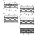
具体的には図1(A)に示すように、第1の基板100上に被剥離層101を形成する
。被剥離層は、最終的に半導体素子、電極、更には液晶層(液晶素子)や発光層(発光素
子)を含む表示機能や駆動回路等を有すればよく、剥離するタイミングと、被剥離層の作
製状態との関係は実施者が決定することができる。例えば図1(A)の被剥離層は、半導
体素子及び当該半導体素子に接続される電極を形成した状態であっても、更に液晶素子や
発光素子を形成した状態であってもよい。Specifically, as shown in FIG. 1 (A), the layer to be peeled 101 is formed on the
第1の基板は後の剥離工程に耐えうる剛性を有していればよく、例えばガラス基板、石
英基板、セラミック基板、シリコン基板、金属基板またはステンレス基板を用いることが
できる。The first substrate may have rigidity that can withstand a later peeling step, and for example, a glass substrate, a quartz substrate, a ceramic substrate, a silicon substrate, a metal substrate, or a stainless steel substrate can be used.
なお被剥離層の半導体素子は、非晶質半導体膜を有するTFT、有機TFT、薄膜ダイ
オード、シリコンのPIN接合からなる光電変換素子、シリコン抵抗素子又はセンサ素子
(代表的にはポリシリコンを用いた感圧式指紋センサ)等であってもよい。さらにTFT
の場合、ボトムゲート型であっても、トップゲート型であってもよい。As the semiconductor element of the peeled layer, a TFT having an amorphous semiconductor film, an organic TFT, a thin film diode, a photoelectric conversion element composed of a PIN junction of silicon, a silicon resistance element or a sensor element (typically polysilicon was used. It may be a pressure-sensitive fingerprint sensor) or the like. Furthermore, TFT
In the case of, it may be a bottom gate type or a top gate type.
次に図1(B)に示すように、被剥離層上に応力緩和材103を形成する。応力緩和材
は剥離工程に必須ではないが、被剥離層を保護するために設けると好ましい。応力緩和材
は水溶性樹脂、熱硬化性樹脂、光硬化性樹脂、その他の樹脂を用いるとよい。すなわち、
被剥離層の保護を目的とするため柔軟性の高い有機樹脂がよく、更に最終的に除去するこ
とを考えると物理的に除去するものでもよいが、水洗、熱又は光により粘着性が低下する
材料がよい。Next, as shown in FIG. 1 (B), the
A highly flexible organic resin is preferable for the purpose of protecting the layer to be peeled off, and it may be physically removed considering that it is finally removed, but the adhesiveness is lowered by washing with water, heat or light. The material is good.
次いで被剥離層の剥離を容易にするため、図1(C)に示すように、第1基板、半導体
素子及び応力緩和材を分断すると好ましい。分断手段は、レーザーやカッター等を用いれ
ばよい。Next, in order to facilitate the peeling of the layer to be peeled off, it is preferable to separate the first substrate, the semiconductor element and the stress relaxation material as shown in FIG. 1 (C). A laser, a cutter, or the like may be used as the dividing means.
分断工程は剥離工程に必須ではないが、剥離を容易に行うために分離する界面の断面を
露出すると好ましい。そして分離する界面の断面にカッター等の物理的手段により傷等を
つけてもよい。また、第1の基板まで分断せず、被剥離層や応力緩和材等に切り込みを入
れてもよい。The splitting step is not essential for the peeling step, but it is preferable to expose the cross section of the interface to be separated in order to facilitate the peeling. Then, the cross section of the interface to be separated may be scratched or the like by a physical means such as a cutter. Further, the first substrate may not be divided, and a cut may be made in the layer to be separated, the stress relaxation material, or the like.
その後図1(D)に示すように、被剥離層上に第2の基板105を張り付ける。このと
き、第1の接着剤106を用いて固定するが、基板自体に接着機能がある場合、接着剤は
必須ではない。第2の基板は、第1の基板よりも剛性の高い基板を用いることが好ましく
、比較的剛性の高い、石英基板を用いるとよい。第1の接着剤は、剥離可能な接着剤、例
えば紫外線により粘着性が低下したり、剥離する紫外線剥離型粘着剤、熱により粘着性が
低下したり、剥離する熱剥離型粘着剤、水洗等により粘着性が低下したり、剥離する水溶
性接着剤や両面テープ等を使用するとよい。After that, as shown in FIG. 1 (D), the
また、剥離工程をより確実にするため、第1の基板下に補助基板108を設けてもよい
。このとき補助基板に接着性がない場合、接着剤107を用いて固定する。なお、第2の
基板と補助基板、及び第1の接着剤と補助基板を固定する接着剤は同一なものを使用すれ
ばよい。Further, in order to make the peeling step more reliable, the
そして図1(E)に示すように、物理的手段を用いて剥離を行う。図1(E)のように
補助基板が設けられている場合は、第2の基板と補助基板とに逆方向に働く力を加えれば
よく、補助基板が設けられていない場合は、粘着性の高いシートを第1の基板下に固定し
て剥離してもよい。Then, as shown in FIG. 1 (E), the peeling is performed by using physical means. When the auxiliary substrate is provided as shown in FIG. 1 (E), a force acting in the opposite direction may be applied to the second substrate and the auxiliary substrate, and when the auxiliary substrate is not provided, the adhesive is adhesive. The tall sheet may be fixed under the first substrate and peeled off.
特に大型基板の場合、均一に剥離するために、圧力差を利用して基板を吸着し剥離して
もよい。すなわち例えば、剥離する基板を空孔が形成された基板上に設置し、ポンプ等に
より当該空孔が減圧又は真空状態とし、剥離する基板全体を圧力差により均一に固定した
状態で剥離を行ってもよい。In particular, in the case of a large substrate, the substrate may be adsorbed and peeled off by utilizing the pressure difference in order to peel off uniformly. That is, for example, the substrate to be peeled off is placed on a substrate on which pores are formed, the pores are reduced in pressure or in a vacuum state by a pump or the like, and the entire substrate to be peeled off is uniformly fixed by a pressure difference before peeling. May be good.
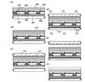
次に図2(F)に示すように、被剥離層下に第3の基板110を固定する。第3の基板
自体に接着性がない場合、第2の接着剤111を介して接着する。第3の基板は、ポリカ
ーボネート、ポリアリレート、ポリエーテルスルフォン等のプラスチック基板、ポリテト
ラフルオロエチレン基板又はセラミック基板等の膜厚の薄い基板や可撓性のある(フレキ
シブルな)基板(以下、これらの基板をフィルム基板と表記する)を用いることができる
。第2の接着剤は、紫外線硬化樹脂、熱硬化樹脂等を用いればよい。但し、第1の接着剤
と第2の接着剤とは、紫外線や熱等により、相反する性質を有する必要がある。すなわち
、紫外線や熱により第1の基板は粘着性が低下、又は剥離し、第2の基板は硬化する必要
がある。図2(F)では、紫外線を照射することにより第1の接着剤の粘着性を低下させ
、第2の接着剤を硬化させている。なお、被剥離層の上下から紫外線を照射しても、一方
の面から紫外線を照射しても構わない。そして図2(G)に示すように、第2の基板を剥
離する。Next, as shown in FIG. 2F, the
このように、紫外線を照射したり、熱を加えるといった同一の工程により、剥離と固定
を同時に行うことができるため、剥離工程を簡略化することができる。As described above, since the peeling and fixing can be performed at the same time by the same step of irradiating with ultraviolet rays or applying heat, the peeling step can be simplified.
次いで図2(H)に示すように、紫外線照射を照射したり、加熱したり、水洗して応力
緩和材を除去する。更に、より正確に除去するためには、アルゴンガス及び酸素ガスを用
いたプラズマクリーニングやベルクリン洗浄を行うと好ましい。このとき、応力緩和材を
第1の接着剤と同一の工程で除去できる材料を使用するとよい。すなわち応力緩和材を紫
外線により除去できる材料とし、第1の接着剤の剥離と、第2の接着剤の硬化と、応力緩
和材の除去とを同時に行ってもよい。そして図2(I)に示すように、被剥離層の第3の
基板への転写が完了する。Then, as shown in FIG. 2H, the stress relaxation material is removed by irradiating with ultraviolet rays, heating, or washing with water. Further, in order to remove the gas more accurately, it is preferable to perform plasma cleaning or berglin cleaning using argon gas and oxygen gas. At this time, it is preferable to use a material that can remove the stress relaxation material in the same process as the first adhesive. That is, the stress relaxation material may be a material that can be removed by ultraviolet rays, and the first adhesive may be peeled off, the second adhesive may be cured, and the stress relaxation material may be removed at the same time. Then, as shown in FIG. 2 (I), the transfer of the layer to be peeled to the third substrate is completed.
このような剥離方法を用いることより、転写のため接着剤の除去や硬化を繰り返す剥離
工程において、工程を簡略化することができる。そして本発明の剥離工程は、全面に剥離
でき、歩留まりよく形成することができる。全面に渡って剥離できることにより、複数の
半導体素子を1つの大型基板に形成し、半導体装置ごとに切断する多面取りを行うことが
でき、コストの低減を期待できる。また本発明では第1の基板等を再利用することができ
、更に安価なフィルム基板を使用するため表示装置の低コスト化を達成することができる
。By using such a peeling method, it is possible to simplify the peeling step in which the adhesive is repeatedly removed and cured for transfer. The peeling step of the present invention can be peeled over the entire surface and can be formed with a good yield. Since it can be peeled off over the entire surface, it is possible to form a plurality of semiconductor elements on one large substrate and perform multi-chamfering for cutting each semiconductor device, and cost reduction can be expected. Further, in the present invention, the first substrate or the like can be reused, and since an inexpensive film substrate is used, the cost of the display device can be reduced.
その結果当該TFT等を有する発光装置、液晶表示装置その他の表示装置は、薄くなり
、落下しても割れにくく、軽量である。また曲面や異形形状での表示が可能となる。As a result, the light emitting device, the liquid crystal display device, and other display devices having the TFT and the like are thin, hard to break even if dropped, and lightweight. In addition, it is possible to display curved surfaces and irregular shapes.
本発明により、同一工程(紫外線の照射や加熱)により、接着剤の剥離(粘着性の低減
も含む)や硬化を行うことができ、剥離工程、強いては表示装置の製造工程を簡略化する
ことができる。更に大型基板から、複数の表示装置を生産する場合に、本発明の剥離工程
に加え、減圧装置等により剥離や転写の工程を正確、かつ簡便に行うことができる。この
ように、本発明の剥離工程により作製工程数が低減され、更に歩留まり良く表示装置を量
産することができる。According to the present invention, the adhesive can be peeled (including reduction of adhesiveness) and cured by the same step (ultraviolet irradiation or heating), and the peeling step, or the manufacturing process of the display device, can be simplified. Can be done. Further, when a plurality of display devices are produced from a large substrate, in addition to the peeling step of the present invention, the peeling and transfer steps can be accurately and easily performed by a decompression device or the like. As described above, the peeling step of the present invention reduces the number of manufacturing steps, and the display device can be mass-produced with a higher yield.
以下に、本発明の実施の形態を図面に基づいて説明する。なお、実施の形態を説明する
ための全図において、同一部分又は同様な機能を有する部分には同一の符号を付し、その
繰り返しの説明は省略する。Hereinafter, embodiments of the present invention will be described with reference to the drawings. In all the drawings for explaining the embodiments, the same parts or parts having the same functions are designated by the same reference numerals, and the repeated description thereof will be omitted.
(実施の形態1)
本実施の形態は、発光素子及び液晶素子までが形成された状態を被剥離層とし、剥離及
び転写を行う場合の具体的な剥離工程及び、本発明の剥離工程により上面出射の発光装置
を形成する一例を説明する。(Embodiment 1)
In the present embodiment, a state in which a light emitting element and a liquid crystal element are formed is used as a layer to be peeled off, and a light emitting device emitted from the upper surface is formed by a specific peeling step in the case of peeling and transfer and a peeling step of the present invention. An example of doing so will be described.
図3(A)に示すように、第1の基板200上に金属膜201を形成する。本実施の形
態では第1の基板は、0.5〜1.0mm程度のガラス基板を用いる。金属膜としては、
W、Ti、Ta、Mo、Nd、Ni、Co、Zr、Zn、Ru、Rh、Pd、Os、Ir
から選ばれた元素または前記元素を主成分とする合金材料若しくは化合物材料からなる単
層、或いはこれらの積層を用いることができる。金属膜の作製方法としてスパッタリング
法を用い、金属をターゲットして、第1の基板上に形成すればよい。なお金属膜の膜厚は
、10nm〜200nm、好ましくは50nm〜75nmとする。As shown in FIG. 3A, the
W, Ti, Ta, Mo, Nd, Ni, Co, Zr, Zn, Ru, Rh, Pd, Os, Ir
A single layer made of an element selected from the above elements or an alloy material or a compound material containing the element as a main component, or a laminate thereof can be used. A sputtering method may be used as a method for producing the metal film, and the metal may be targeted and formed on the first substrate. The film thickness of the metal film is 10 nm to 200 nm, preferably 50 nm to 75 nm.
金属膜に上記金属の合金(例えば、WとMoとの合金:WxMo1−X)を用いる場合
、成膜室内に第1の金属(W)及び第2の金属(Mo)といった複数のターゲット、又は
第1の金属(W)と第2の金属(Mo)との合金のターゲットを配置してスパッタリング
法により形成すればよい。このように、金属膜の形成を適宜設定することにより、剥離工
程を制御することができ、プロセスマージンが広がる。例えば、金属の合金を用いた場合
、合金の各金属の組成比を制御することにより、加熱処理の温度、更には加熱処理の要否
を制御することができうる。When an alloy of the above metals (for example, an alloy of W and Mo: Wx Mo1-X ) is used for the metal film, a plurality of metals (W) and a second metal (Mo) are used in the film forming chamber. A target or a target of an alloy of a first metal (W) and a second metal (Mo) may be arranged and formed by a sputtering method. By appropriately setting the formation of the metal film in this way, the peeling process can be controlled and the process margin is widened. For example, when a metal alloy is used, the temperature of the heat treatment and the necessity of the heat treatment can be controlled by controlling the composition ratio of each metal of the alloy.
金属膜の代わりに、窒化された金属膜(窒化金属膜)を用いても構わない。更に、金属
膜に窒素や酸素を添加してもよい。例えば、金属膜に窒素や酸素をイオン注入したり、成
膜室を窒素や酸素雰囲気とし、スパッタリング法により金属膜を形成したり、更にターゲ
ットとして窒化金属を用いてもよい。A nitrided metal film (metal nitride film) may be used instead of the metal film. Further, nitrogen or oxygen may be added to the metal film. For example, nitrogen or oxygen may be ion-implanted into the metal film, the film forming chamber may be set to a nitrogen or oxygen atmosphere, the metal film may be formed by a sputtering method, or a metal nitride may be used as a target.
その後、金属膜201上に積層した下地膜207を介して半導体膜を形成する。すなわ
ち、金属膜と半導体膜との間には下地膜を代表とする絶縁膜が何層設けてもよい。下地膜
は、酸化シリコン膜、窒化シリコン膜または酸化窒化シリコン膜などの珪素を有する絶縁
膜の単層、又は積層膜を用いればよい。本実施の形態では、金属膜上にスパッタリング法
により形成される150nm〜200nmのSiO2と、SiO2上にCVD法により形
成される80〜100nmのSiONとを設ける。下地膜により、基板や金属膜から半導
体膜への不純物拡散を防止することができる。After that, a semiconductor film is formed via the
なお上述の工程を経ると、金属膜表面には当該金属を有する酸化膜(酸化金属膜)20
2が形成される。酸化金属膜の膜厚は、0.1nm〜1μm、好ましくは0.1nm〜1
00nm、更に好ましくは0.1nm〜5nmとなるようにすればよい。また金属膜上に
直接酸化膜を作製してもよい。After the above steps, the oxide film (metal oxide film) 20 having the metal on the surface of the metal film is 20.
2 is formed. The film thickness of the metal oxide film is 0.1 nm to 1 μm, preferably 0.1 nm to 1
It may be 00 nm, more preferably 0.1 nm to 5 nm. Further, an oxide film may be formed directly on the metal film.
その後必要に応じて、加熱処理を行う。この加熱処理により、酸化金属膜が結晶化し、
結晶歪みや格子欠陥(点欠陥、線欠陥、面欠陥(例えば、酸素空孔が集まってできる結晶
学的せん断面による面欠陥)、拡張欠陥)が生じ、剥離しやすい状態とすることができる
。Then, if necessary, heat treatment is performed. By this heat treatment, the metal oxide film crystallizes and
Crystal distortion and lattice defects (point defects, line defects, surface defects (for example, surface defects due to crystallographic shear surfaces formed by gathering oxygen vacancies), expansion defects) can occur, and the state can be easily peeled off.
更に加熱処理により、半導体膜が有する水素が拡散することによる酸化還元反応により
、結晶状態の異なる酸化金属が形成され、より剥離しやすい状態とすることも考えられる
。Further, it is also conceivable that the heat treatment causes the redox reaction due to the diffusion of hydrogen contained in the semiconductor film to form a metal oxide having a different crystal state, which makes it easier to peel off.
なお、上記加熱処理は半導体膜の結晶化の加熱処理と兼ねることができる。すなわち、
金属膜上に形成された半導体膜を加熱しすることにより、結晶性半導体膜を形成し、且つ
酸化金属膜の結晶化を行うことが可能である。The heat treatment can also be used as a heat treatment for crystallization of the semiconductor film. That is,
By heating the semiconductor film formed on the metal film, it is possible to form a crystalline semiconductor film and crystallize the metal oxide film.
半導体膜の結晶性を向上させるために、結晶化を助長させる金属元素(代表的にはNi
元素)を塗布後加熱処理したり、加熱処理後にレーザーを照射してもよい。なお、結晶化
を助長される金属元素を使用した場合、当該金属元素はデバイスにとっては不要なもので
あるため、ゲッタリング工程やエッチング工程により除去することが望まれる。A metal element (typically Ni) that promotes crystallization in order to improve the crystallinity of the semiconductor film.
The element) may be applied and then heat-treated, or the heat treatment may be followed by irradiation with a laser. When a metal element that promotes crystallization is used, it is desirable to remove the metal element by a gettering step or an etching step because the metal element is unnecessary for the device.
その後、結晶性半導体膜を所望の形状にパターニングし、珪素を有する酸化膜、又は珪
素を有する窒化膜を用いてゲート絶縁膜を形成する。ゲート絶縁膜を介して結晶性半導体
膜上にゲート電極を形成し、当該ゲート電極をマスクとして不純物領域を形成する。ゲー
ト電極にはWとTaNの積層構造を用い、不純物領域にはソース及びドレイン領域と、低
濃度不純物領域(LDD領域)と、ゲート電極と重なる低濃度不純物領域(GOLD領域
)とを設けてもよい。そしてTFT203が形成される。Then, the crystalline semiconductor film is patterned into a desired shape, and a gate insulating film is formed by using an oxide film having silicon or a nitride film having silicon. A gate electrode is formed on the crystalline semiconductor film via the gate insulating film, and an impurity region is formed using the gate electrode as a mask. A laminated structure of W and TaN may be used for the gate electrode, and a source and drain regions, a low-concentration impurity region (LDD region), and a low-concentration impurity region (GOLD region) overlapping the gate electrode may be provided as the impurity region. good. Then, the
次いでソース配線又はドレイン配線と接続される電極204を形成する。そして電極2
04の端を覆う、すなわち隣り合う電極の両端を覆うように有機材料や無機材料を有する
絶縁膜205を形成する。そして、水分や酸素の侵入を防ぐために、絶縁膜上に保護膜2
06を形成する。Next, the
An insulating
Form 06.
以上のように、半導体素子としてTFTを形成する。各画素にTFTを形成するアクテ
ィブマトリクス型表示装置を説明しているが、パッシブ型表示装置でもよいことは言うま
でもない。またトップゲート型のTFTでも、ボトムゲート型のTFTでも構わない。As described above, the TFT is formed as a semiconductor element. Although the active matrix type display device that forms the TFT in each pixel is described, it goes without saying that the passive type display device may be used. Further, a top gate type TFT or a bottom gate type TFT may be used.
なお被剥離層の半導体素子は、非晶質半導体膜を有するTFT、有機TFT、薄膜ダイ
オード、シリコンのPIN接合からなる光電変換素子、シリコン抵抗素子又はセンサ素子
(代表的にはポリシリコンを用いた感圧式指紋センサ)等であってもよい。As the semiconductor element of the peeled layer, a TFT having an amorphous semiconductor film, an organic TFT, a thin film diode, a photoelectric conversion element composed of a PIN junction of silicon, a silicon resistance element or a sensor element (typically polysilicon was used. It may be a pressure-sensitive fingerprint sensor) or the like.
その後図3(B)に示すように、発光層208及び陰極210を形成する。発光層は各
RGB発光層を形成しても、白色発光層を形成し、カラーフィルター等の色変換層により
多色表示を行ってもよい。陰極は上面出射の場合は透光性を有する材料、例えばITOで
、下面出射の場合はMgAg等の金属膜で形成すればよい。なお、大気に曝さずに発光層
、陰極等までを連続して形成すると好ましい。After that, as shown in FIG. 3B, the
有機化合物を含む発光層の形成前又は形成後には、真空加熱を行って脱気を行うことが
好ましい。また有機化合物を含む発光層208は、極めて薄いため、第1の電極の表面は
平坦であることが好ましく、化学的及び機械的に研磨する処理(代表的にはCMP技術等
)により平坦化を行うとよい。Before or after the formation of the light emitting layer containing the organic compound, it is preferable to perform vacuum heating to degas. Further, since the
電極204の表面における清浄度を向上させるため、異物(ゴミなど)をクリーニング
するための洗浄(ブラシ洗浄やベルクリン洗浄)やプラズマクリーニングを発光層形成前
に行ってもよい。このとき、転写に使用した接着剤の付着もきれいに除去することができ
る。In order to improve the cleanliness on the surface of the
そして、以下に示すように剥離が行われる。なお、本実施の形態では発光素子(発光層
及び陰極や陽極)を形成した後に剥離する場合を説明するが、電極204が形成された後
に剥離してもよい。すなわち剥離するタイミングは実施者が適宜決定することができる。Then, peeling is performed as shown below. In the present embodiment, the case where the light emitting element (light emitting layer and the cathode or the anode) is formed and then peeled off will be described, but the
図3(C)に示すように、陰極上に保護膜213を形成する。保護膜はDLC、CN、
SiN等の炭素や窒素を有する膜を形成すればよい。
保護膜上には紫外線(UV)防止膜216を形成し、紫外線の照射から発光層を保護する
。特に、上面出射の発光装置では、必然的に発光層に紫外線が照射されてしまうため、紫
外線防止膜(UV防止膜)を設け、発光層の劣化を防止する。すなわちUV防止膜は、U
V領域の波長を透過せず(少なくとも90%以上透過しない)、発光層からの光、つまり
可視光程度の領域(400nm〜1μm、好ましくは450nm〜800nm)の波長を
透過する性質を有するフィルム(シート)を用いればよい。例えば、紫外線吸収剤を配合
させた有機樹脂フィルム、具体的にはポリエチレンテレフタレートやポリエチレン−2、
6−ナフタレンジカルボキシレート等のポリエステルのフィルムを用いればよい。ポリエ
ステルのフィルムは公知の押し出し法等により形成すればよい。また紫外線を吸収する層
と、その他層を積層した構造の有機樹脂フィルムを用いても構わない。As shown in FIG. 3C, a
A film having carbon or nitrogen such as SiN may be formed.
An ultraviolet (UV) preventing
A film that does not transmit wavelengths in the V region (does not transmit at least 90% or more), but transmits light from the light emitting layer, that is, wavelengths in the visible light region (400 nm to 1 μm, preferably 450 nm to 800 nm). Sheet) may be used. For example, an organic resin film containing an ultraviolet absorber, specifically polyethylene terephthalate or polyethylene-2.
A polyester film such as 6-naphthalene carboxylate may be used. The polyester film may be formed by a known extrusion method or the like. Further, an organic resin film having a structure in which a layer that absorbs ultraviolet rays and another layer are laminated may be used.
そして図3(D)に示すように、スピンコーティング法により、応力緩和材として水溶
性樹脂217を形成する。応力緩和材は、熱を加えたり、紫外線を照射して硬化させれば
よい。また紫外線を照射して硬化する材料を使用する場合、応力緩和材の上方から紫外線
を照射するとき、UV防止膜により発光層を保護することができる。Then, as shown in FIG. 3D, the water-
その後、剥離を容易に行うため、分断したり、剥離界面に傷を付けたりするとよい。図
示しないが、本実施の形態ではカッターの一種であるスクライブトリガーにより第1の基
板、被剥離層及び水溶性樹脂を分断し、剥離界面の断面を露出させる。After that, in order to easily perform peeling, it is advisable to divide or scratch the peeling interface. Although not shown, in the present embodiment, the first substrate, the layer to be peeled, and the water-soluble resin are separated by a scribe trigger, which is a kind of cutter, to expose the cross section of the peeling interface.
そして図3(E)に示すように、第2の基板211を水溶性樹脂上に設ける。本実施の
形態では、第2の基板に接着性を有しない石英基板(厚さ1.0〜1.5mm)を使用し
、両面テープ212を用いて固定する。剥離工程で使用される両面テープは、紫外線を照
射したり、加熱したり、水等の液体に浸漬することにより、粘着性が低下したり、自己剥
離する性質を有する。本実施の形態では、紫外線を照射すると粘着性を低下する両面テー
プを用いる。Then, as shown in FIG. 3 (E), the
両面テープの代わりに紫外線硬化樹脂、具体的にはエポキシ樹脂系接着剤、熱硬化樹脂
や樹脂添加剤等の接着剤を用いてもよい。また補助基板として、第1の基板下に両面テー
プや接着剤等を用いて石英基板を固定してもよい。Instead of the double-sided tape, an ultraviolet curable resin, specifically an adhesive such as an epoxy resin adhesive, a thermosetting resin, or a resin additive may be used. Further, as the auxiliary substrate, the quartz substrate may be fixed under the first substrate by using double-sided tape, an adhesive or the like.
その後図3(F)に示すように、第1の基板と半導体素子を有する被剥離層とを物理的
手段により分離する。酸化金属膜と金属膜との界面で剥離するよう図示しているが、この
とき結晶化された酸化金属膜の膜内、又は酸化金属膜の両面の界面、すなわち酸化金属膜
と金属膜との界面或いは酸化金属膜と被剥離層との界面等から分離している。酸化金属膜
の内部で分離する場合、被剥離層の下面には酸化金属が点在して付着していることがある
。また酸化金属膜と金属膜との界面或いは酸化金属膜と被剥離層との界面で分離する場合
、酸化金属膜は被剥離層の下面のみに存在したり、金属膜上面のみに存在するときがある
。酸化金属物が被剥離層の下面に点在したり、付着しする場合、酸化金属物はエッチング
又は化学的若しくは物理的研磨により除去してもよいし、付着させたままでもよい。After that, as shown in FIG. 3 (F), the first substrate and the layer to be peeled off having the semiconductor element are separated by physical means. It is shown to be peeled off at the interface between the metal oxide film and the metal film, but at this time, the inside of the crystallized metal oxide film or the interface on both sides of the metal oxide film, that is, the metal oxide film and the metal film It is separated from the interface or the interface between the metal oxide film and the layer to be peeled off. When separated inside the metal oxide film, metal oxide may be scattered and adhered to the lower surface of the layer to be peeled off. When the metal oxide film is separated at the interface between the metal oxide film and the metal film or the interface between the metal oxide film and the peeled layer, the metal oxide film may be present only on the lower surface of the peeled layer or only on the upper surface of the metal film. be. When the metal oxide is scattered or adhered to the lower surface of the layer to be peeled off, the metal oxide may be removed by etching or chemical or physical polishing, or may be left attached.
次に図3(G)に示すように、被剥離層を第3の基板であるフィルム基板214に固定
する。フィルム基板が粘着性を有していない場合、第2の接着剤215を介して固定する
。第2の接着剤には、紫外線硬化樹脂、具体的にはエポキシ樹脂系接着剤、熱硬化樹脂や
樹脂添加剤等の接着剤または両面テープを用いることができる。本実施の形態では第2の
接着剤として、紫外線照射により硬化する非水溶性接着剤を用いる。すなわち第2の接着
剤は、応力緩和材を除去する場合のことを考えて、応力緩和材の性質を考慮し、剥離しな
い材料を用いる必要がある。もちろん応力緩和材は必ずしも除去しなくてよい。Next, as shown in FIG. 3 (G), the peeled layer is fixed to the
すなわち本実施の形態は、第1の接着剤の粘着性が低下したり、剥離する要因と、第2
の接着剤が硬化する要因とが同一な接着剤を用いる。例えば、紫外線照射により粘着性が
低下する接着剤と、硬化する接着剤とを用いると、一度の紫外線照射により、第2の基板
の剥離と、第3の基板への固定とを行うことができ、工程を簡略化することができる。That is, in the present embodiment, the adhesiveness of the first adhesive is lowered or peeled off, and the second is
Use an adhesive that is the same as the factor that causes the adhesive to cure. For example, by using an adhesive whose adhesiveness is lowered by irradiation with ultraviolet rays and an adhesive which is cured, it is possible to peel off the second substrate and fix it to the third substrate by one irradiation with ultraviolet rays. , The process can be simplified.
そして図3(H)に示すように、第2の基板を分離する。このとき第1の接着剤の粘着
性は低下しているため、容易、かつ正確に剥離を行うことができる。Then, as shown in FIG. 3 (H), the second substrate is separated. At this time, since the adhesiveness of the first adhesive is reduced, the peeling can be easily and accurately performed.
次いで図3(I)に示すように、水溶性樹脂を除去する。本実施の形態では水溶性樹脂
を除去するため、第3の基板に固定された被剥離層を純水へ浸漬させる。すると、水溶性
樹脂のみ除去される。その後UV防止膜上に封止膜232を形成し、第3の基板に被剥離
層が転写され、上面出射の発光装置が完成する。Then, as shown in FIG. 3 (I), the water-soluble resin is removed. In this embodiment, in order to remove the water-soluble resin, the layer to be peeled off fixed to the third substrate is immersed in pure water. Then, only the water-soluble resin is removed. After that, the sealing
また第1及び第2の接着剤、応力緩和材をより精度よく除去するためには、アルゴンガ
ス及び酸素ガスを用いたプラズマクリーニングやベルクリン洗浄を行うとよい。Further, in order to remove the first and second adhesives and stress relaxation materials more accurately, plasma cleaning or berglin cleaning using argon gas and oxygen gas may be performed.
以上のように、簡略化された剥離工程により、フィルム基板上に形成されたTFT等を
有する発光装置を形成することができる。その結果、薄型で軽量、落としても破壊しにく
く、そしてフレキシブルな発光装置を提供することができる。As described above, a light emitting device having a TFT or the like formed on a film substrate can be formed by a simplified peeling step. As a result, it is possible to provide a light emitting device that is thin and lightweight, is not easily destroyed even if dropped, and is flexible.
またフィルム基板へ、発光装置の各用途に応じたTFT等が設けられた複数の被剥離層
を、転写してもよい。例えば、画素部用のTFTと、駆動回路用のTFTとの被剥離層を
形成し、フィルム基板の所定領域へ転写してもよい。Further, a plurality of layers to be peeled off, which are provided with TFTs or the like according to each use of the light emitting device, may be transferred to the film substrate. For example, a peelable layer of the TFT for the pixel portion and the TFT for the drive circuit may be formed and transferred to a predetermined region of the film substrate.
また本実施の形態では、上面出射の発光装置の場合を説明したが、下面出射の発光装置
であっても本発明を適応できることは言うまでもない。Further, in the present embodiment, the case of the light emitting device emitted from the upper surface has been described, but it goes without saying that the present invention can be applied even to the light emitting device emitted from the lower surface.
(実施の形態2)
本実施の形態では、発光素子及び液晶素子まで形成された状態を被剥離層とし、剥離及
び転写を行う場合であって、紫外線と熱を加えて接着剤の粘着性を制御する場合の剥離工
程を用い下面出射の発光装置を形成する一例を説明する。また実施の形態1と同様の工程
や材料の説明を省略する。(Embodiment 2)
In the present embodiment, the peeling step is a case where the layer to be peeled is a state in which the light emitting element and the liquid crystal element are formed, and peeling and transfer are performed, and the adhesiveness of the adhesive is controlled by applying ultraviolet rays and heat. An example of forming a light emitting device that emits light from the bottom surface will be described. Further, the description of the same steps and materials as in the first embodiment will be omitted.
まず実施の形態1と同様に保護膜213まで形成する(図4(A))。但し下面出射の
発光装置であるため、電極204には透光性を有する材料を使用する必要がある。また応
力緩和材を設けてもよいが、本実施の形態では特に設けない。First, the
次いで図4(B)に示すように、保護膜213上に接着剤として両面テープ212を用
いて第2の基板211を固定し、その後第1の基板200を剥離する。Next, as shown in FIG. 4B, the
そして図4(C)に示すように、第3の基板であるフィルム基板214を接着剤215
により被剥離層下に張り付ける。本実施の形態では、加熱により粘着性が低下又は剥離す
る両面テープを用い、紫外線により硬化する接着剤を用いるため、紫外線をフィルム基板
の下面から照射しながら、加熱する。もちろん紫外線は基板の両面から照射してもよい。
更には、電極が紫外線を透過する場合、第2の基板の上方から照射しても構わない。もち
ろん、紫外線により粘着性が低下又は剥離する両面テープを用い、加熱による硬化する接
着剤を使用してもよく、紫外線を第2の基板の上方から照射するのが適すであろう。Then, as shown in FIG. 4C, the
It is attached under the layer to be peeled off. In the present embodiment, a double-sided tape whose adhesiveness is reduced or peeled off by heating is used, and an adhesive that is cured by ultraviolet rays is used. Therefore, heating is performed while irradiating ultraviolet rays from the lower surface of the film substrate. Of course, ultraviolet rays may be irradiated from both sides of the substrate.
Further, when the electrode transmits ultraviolet rays, it may be irradiated from above the second substrate. Of course, a double-sided tape whose adhesiveness is reduced or peeled off by ultraviolet rays may be used, and an adhesive which is cured by heating may be used, and it is suitable to irradiate the ultraviolet rays from above the second substrate.
本実施の形態のように、紫外線の照射と加熱を行うことにより、両面テープ212の粘
着性の低下や剥離の要因と、接着剤の硬化の要因とが、異なっていても、同一工程で剥離
と硬化を行うことができ、剥離工程を簡略化することができる。By irradiating and heating with ultraviolet rays as in the present embodiment, even if the factors of deterioration and peeling of the double-
その後図4(D)に示すように、第2の基板を剥離する。そして図4(E)に示すよう
に、封止膜232を形成し、下面出射の発光装置が完成する。After that, as shown in FIG. 4D, the second substrate is peeled off. Then, as shown in FIG. 4 (E), the sealing
以上のように、簡略化された剥離工程により、フィルム基板上に形成されたTFT等を
有する発光装置として使用することができる。その結果、薄型で軽量、落としても破壊し
にくく、かつフレキシブルな発光装置を提供することができる。As described above, by the simplified peeling step, it can be used as a light emitting device having a TFT or the like formed on a film substrate. As a result, it is possible to provide a light emitting device that is thin and lightweight, is not easily destroyed even if dropped, and is flexible.
また本実施の形態では、下面出射の発光装置の場合を説明したが、上面出射の発光装置
であっても本発明を適応できることは言うまでもない。また上面出射の場合、発光層の劣
化を防ぐためにUV防止膜を設けるとよい。Further, in the present embodiment, the case of the light emitting device emitted from the bottom surface has been described, but it goes without saying that the present invention can be applied even to the light emitting device emitted from the top surface. Further, in the case of top emission, it is advisable to provide a UV protection film in order to prevent deterioration of the light emitting layer.
(実施の形態3)
本実施の形態では、半導体素子、電極、及び絶縁膜等までが形成された状態を被剥離層
とし、剥離及び転写を行う場合の発光装置の作製方法について説明する。(Embodiment 3)
In the present embodiment, a method of manufacturing a light emitting device in the case of performing peeling and transfer by using a state in which a semiconductor element, an electrode, an insulating film, and the like are formed as a peeling layer will be described.
図12(A)に示すように、第1の基板200上に金属膜201を形成する。本実施の
形態では第1の基板は、0.5〜1.0mm程度のガラス基板を用いる。金属膜としては
、W、Ti、Ta、Mo、Nd、Ni、Co、Zr、Zn、Ru、Rh、Pd、Os、I
rから選ばれた元素または前記元素を主成分とする合金材料若しくは化合物材料からなる
単層、或いはこれらの積層を用いることができる。金属膜の作製方法としてスパッタリン
グ法を用い、金属をターゲットして、第1の基板上に形成すればよい。なお金属膜の膜厚
は、10nm〜200nm、好ましくは50nm〜75nmとする。As shown in FIG. 12A, the
A single layer made of an element selected from r or an alloy material or a compound material containing the element as a main component, or a laminate thereof can be used. A sputtering method may be used as a method for producing the metal film, and the metal may be targeted and formed on the first substrate. The film thickness of the metal film is 10 nm to 200 nm, preferably 50 nm to 75 nm.
金属膜に上記金属の合金(例えば、WとMoとの合金:WxMo1−X)を用いる場合
、成膜室内に第1の金属(W)及び第2の金属(Mo)といった複数のターゲット、又は
第1の金属(W)と第2の金属(Mo)との合金のターゲットを配置してスパッタリング
法により形成すればよい。このように、金属膜の形成を適宜設定することにより、剥離工
程を制御することができ、プロセスマージンが広がる。例えば、金属の合金を用いた場合
、合金の各金属の組成比を制御することにより、加熱処理の温度、更には加熱処理の要否
を制御することができうる。When an alloy of the above metals (for example, an alloy of W and Mo: Wx Mo1-X ) is used for the metal film, a plurality of metals (W) and a second metal (Mo) are used in the film forming chamber. A target or a target of an alloy of a first metal (W) and a second metal (Mo) may be arranged and formed by a sputtering method. By appropriately setting the formation of the metal film in this way, the peeling process can be controlled and the process margin is widened. For example, when a metal alloy is used, the temperature of the heat treatment and the necessity of the heat treatment can be controlled by controlling the composition ratio of each metal of the alloy.
金属膜の代わりに、窒化された金属膜(窒化金属膜)を用いても構わない。更に、金属
膜に窒素や酸素を添加してもよい。例えば、金属膜に窒素や酸素をイオン注入したり、成
膜室を窒素や酸素雰囲気とし、スパッタリング法により金属膜を形成したり、更にターゲ
ットとして窒化金属を用いてもよい。A nitrided metal film (metal nitride film) may be used instead of the metal film. Further, nitrogen or oxygen may be added to the metal film. For example, nitrogen or oxygen may be ion-implanted into the metal film, the film forming chamber may be set to a nitrogen or oxygen atmosphere, the metal film may be formed by a sputtering method, or a metal nitride may be used as a target.
その後、金属膜201上に積層した下地膜207を介して半導体膜を形成する。すなわ
ち、金属膜と半導体膜との間には下地膜を代表とする絶縁膜が何層設けてもよい。下地膜
は、酸化シリコン膜、窒化シリコン膜または酸化窒化シリコン膜などの珪素を有する絶縁
膜の単層、又は積層膜を用いればよい。本実施の形態では、金属膜上にスパッタリング法
により形成される150nm〜200nmのSiO2と、SiO2上にCVD法により形
成される80〜100nmのSiONとを設ける。下地膜により、基板や金属膜から半導
体膜への不純物拡散を防止することができる。After that, a semiconductor film is formed via the
なお上述の工程を経ると、金属膜表面には当該金属を有する酸化膜(酸化金属膜)20
2が形成される。酸化金属膜の膜厚は、0.1nm〜1μm、好ましくは0.1nm〜1
00nm、更に好ましくは0.1nm〜5nmとなるようにすればよい。また金属膜上に
直接酸化膜を作製してもよい。After the above steps, the oxide film (metal oxide film) 20 having the metal on the surface of the metal film is 20.
2 is formed. The film thickness of the metal oxide film is 0.1 nm to 1 μm, preferably 0.1 nm to 1
It may be 00 nm, more preferably 0.1 nm to 5 nm. Further, an oxide film may be formed directly on the metal film.
その後必要に応じて、加熱処理を行う。この加熱処理により、酸化金属膜が結晶化し、
結晶歪みや格子欠陥(点欠陥、線欠陥、面欠陥(例えば、酸素空孔が集まってできる結晶
学的せん断面による面欠陥)、拡張欠陥)が生じ、剥離しやすい状態とすることができる
。Then, if necessary, heat treatment is performed. By this heat treatment, the metal oxide film crystallizes and
Crystal distortion and lattice defects (point defects, line defects, surface defects (for example, surface defects due to crystallographic shear surfaces formed by gathering oxygen vacancies), expansion defects) can occur, and the state can be easily peeled off.
更に加熱処理により、半導体膜が有する水素が拡散することによる酸化還元反応により
、結晶状態の異なる酸化金属が形成され、より剥離しやすい状態とすることも考えられる
。Further, it is also conceivable that the heat treatment causes the redox reaction due to the diffusion of hydrogen contained in the semiconductor film to form a metal oxide having a different crystal state, which makes it easier to peel off.
なお、上記加熱処理は半導体膜の結晶化の加熱処理と兼ねることができる。すなわち、
金属膜上に形成された半導体膜を加熱しすることにより、結晶性半導体膜を形成し、且つ
酸化金属膜の結晶化を行うことが可能である。The heat treatment can also be used as a heat treatment for crystallization of the semiconductor film. That is,
By heating the semiconductor film formed on the metal film, it is possible to form a crystalline semiconductor film and crystallize the metal oxide film.
半導体膜の結晶性を向上させるために、結晶化を助長させる金属元素(代表的にはNi
元素)を塗布後加熱処理したり、加熱処理後にレーザーを照射してもよい。なお、結晶化
を助長される金属元素を使用した場合、当該金属元素はデバイスにとっては不要なもので
あるため、ゲッタリング工程やエッチング工程により除去することが望まれる。A metal element (typically Ni) that promotes crystallization in order to improve the crystallinity of the semiconductor film.
The element) may be applied and then heat-treated, or the heat treatment may be followed by irradiation with a laser. When a metal element that promotes crystallization is used, it is desirable to remove the metal element by a gettering step or an etching step because the metal element is unnecessary for the device.
その後、結晶性半導体膜を所望の形状にパターニングし、珪素を有する酸化膜、又は珪
素を有する窒化膜を用いてゲート絶縁膜を形成する。ゲート絶縁膜を介して結晶性半導体
膜上にゲート電極を形成し、当該ゲート電極をマスクとして不純物領域を形成する。ゲー
ト電極にはWとTaNの積層構造を用い、不純物領域にはソース及びドレイン領域と、低
濃度不純物領域(LDD領域)と、ゲート電極と重なる低濃度不純物領域(GOLD領域
)とを設けてもよい。そしてTFT203が形成される。Then, the crystalline semiconductor film is patterned into a desired shape, and a gate insulating film is formed by using an oxide film having silicon or a nitride film having silicon. A gate electrode is formed on the crystalline semiconductor film via the gate insulating film, and an impurity region is formed using the gate electrode as a mask. A laminated structure of W and TaN may be used for the gate electrode, and a source and drain regions, a low-concentration impurity region (LDD region), and a low-concentration impurity region (GOLD region) overlapping the gate electrode may be provided as the impurity region. good. Then, the
次いでソース配線又はドレイン配線と接続される電極204を形成する。そして電極2
04の端を覆う、すなわち隣り合う電極の両端を覆うように有機材料や無機材料を有する
絶縁膜205を形成する。絶縁膜としては、アクリル膜(感光性アクリルを含む)の他に
ポリイミド、ポリアミド、BCB(ベンゾシクロブテン)といった有機材料、又は酸化シ
リコン膜の他に、窒化シリコン膜、窒化酸化シリコン膜および塗布シリコン酸化膜(SO
G:Spin On Glass)等のシリコンを含む無機材料を用いることができる。
本実施の形態では感光性アクリルを用いる。絶縁膜形成後、エッチングにより開口部を形
成し電極204を露出させる。そして、絶縁膜、特に有機材料を有する絶縁膜は発光素子
の劣化要因となる水分や酸素等が侵入しやすいため、絶縁膜上に保護膜206を形成する
。保護膜はDLC、CN、SiN等の炭素や窒素を有する膜を形成すればよい。Next, the
An insulating
Inorganic materials containing silicon such as G: Spin On Glass) can be used.
In this embodiment, photosensitive acrylic is used. After forming the insulating film, an opening is formed by etching to expose the
以上のように、半導体素子としてTFTを形成する。各画素にTFTを形成するアクテ
ィブマトリクス型表示装置を説明しているが、パッシブ型表示装置でもよいことは言うま
でもない。
なお被剥離層の半導体素子は、有機TFT、薄膜ダイオード、シリコンのPIN接合から
なる光電変換素子、シリコン抵抗素子又はセンサ素子(代表的にはポリシリコンを用いた
感圧式指紋センサ)等であってもよい。As described above, the TFT is formed as a semiconductor element. Although the active matrix type display device that forms the TFT in each pixel is described, it goes without saying that the passive type display device may be used.
The semiconductor element of the peeled layer is an organic TFT, a thin film diode, a photoelectric conversion element composed of a PIN junction of silicon, a silicon resistance element or a sensor element (typically, a pressure-sensitive fingerprint sensor using polysilicon) and the like. May be good.
そして、以下に示すように剥離が行われる。なお、本実施の形態では電極及び絶縁膜等
を形成した後に剥離する場合を説明するが、絶縁膜形成後、発光層を形成した後剥離して
もよい。すなわち剥離するタイミングは実施者が適宜決定することができる。
そして図12(B)に示すように、電極、絶縁膜及び保護膜を覆ってスピンコーティング
法により、応力緩和材として水溶性樹脂209を形成する。応力緩和材は、熱を加えたり
、紫外線を照射して硬化させればよい。また紫外線を照射して硬化する材料を使用する場
合であって、半導体素子の劣化が懸念されるときは、紫外線防止膜(UV防止膜)により
保護することができる。Then, peeling is performed as shown below. In this embodiment, the case where the electrode, the insulating film, and the like are formed and then peeled off will be described, but the insulating film may be formed, and then the light emitting layer may be formed and then peeled off. That is, the timing of peeling can be appropriately determined by the practitioner.
Then, as shown in FIG. 12B, the water-
UV防止膜は、紫外線領域(UV領域)の波長を透過せず(少なくとも90%以上透過
しない)、発光層からの光、つまり可視光程度の領域(400nm〜1μm、好ましくは
450nm〜800nm)の波長を透過する性質を有するフィルム(シート)を用いれば
よい。例えば、紫外線吸収剤を配合させた有機樹脂フィルム、具体的にはポリエチレンテ
レフタレートやポリエチレン−2、6−ナフタレンジカルボキシレート等のポリエステル
のフィルムを用いればよい。ポリエステルのフィルムは公知の押し出し法等により形成す
ればよい。また紫外線を吸収する層と、その他層を積層した構造の有機樹脂フィルムを用
いても構わない。The UV protection film does not transmit the wavelength of the ultraviolet region (UV region) (it does not transmit at least 90% or more), and the light from the light emitting layer, that is, the region of visible light (400 nm to 1 μm, preferably 450 nm to 800 nm). A film (sheet) having a property of transmitting a wavelength may be used. For example, an organic resin film containing an ultraviolet absorber, specifically, a polyester film such as polyethylene terephthalate or polyethylene-2 or 6-naphthalenedicarboxylate may be used. The polyester film may be formed by a known extrusion method or the like. Further, an organic resin film having a structure in which a layer that absorbs ultraviolet rays and another layer are laminated may be used.
その後、剥離を容易に行うため、分断したり、剥離界面に傷を付けたりするとよい。図
示しないが、本実施の形態ではカッターの一種であるスクライブトリガーにより第1の基
板、被剥離層及び水溶性樹脂を分断し、剥離界面の断面を露出させる。After that, in order to easily perform peeling, it is advisable to divide or scratch the peeling interface. Although not shown, in the present embodiment, the first substrate, the layer to be peeled, and the water-soluble resin are separated by a scribe trigger, which is a kind of cutter, to expose the cross section of the peeling interface.
そして図12(C)に示すように、第2の基板211を水溶性樹脂上に設ける。本実施
の形態では、第2の基板に接着性を有しない石英基板(厚さ1.0〜1.5mm)を使用
し、両面テープ212を用いて固定する。剥離工程で使用される両面テープは、紫外線を
照射したり、加熱したり、水等の液体に浸漬することにより、粘着性が低下したり、自己
剥離する性質を有する。本実施の形態では、紫外線を照射すると粘着性を低下する両面テ
ープを用いる。Then, as shown in FIG. 12C, the
両面テープの代わりに紫外線硬化樹脂、具体的にはエポキシ樹脂系接着剤、熱硬化樹脂
や樹脂添加剤等の接着剤を用いてもよい。また補助基板として、第1の基板下に両面テー
プや接着剤等を用いて石英基板を固定してもよい。Instead of the double-sided tape, an ultraviolet curable resin, specifically an adhesive such as an epoxy resin adhesive, a thermosetting resin, or a resin additive may be used. Further, as the auxiliary substrate, the quartz substrate may be fixed under the first substrate by using double-sided tape, an adhesive or the like.
その後図12(D)に示すように、第1の基板と半導体素子を有する被剥離層とを物理
的手段により分離する。酸化金属膜と金属膜との界面で剥離するよう図示しているが、こ
のとき結晶化された酸化金属膜の膜内、又は酸化金属膜の両面の界面、すなわち酸化金属
膜と金属膜との界面或いは酸化金属膜と被剥離層との界面等から分離している。酸化金属
膜の内部で分離する場合、被剥離層の下面には酸化金属が点在して付着していることがあ
る。また酸化金属膜と金属膜との界面或いは酸化金属膜と被剥離層との界面で分離する場
合、酸化金属膜は被剥離層の下面のみに存在したり、金属膜上面のみに存在するときがあ
る。酸化金属物が被剥離層の下面に点在したり、付着しする場合、酸化金属物はエッチン
グ又は化学的若しくは物理的研磨により除去してもよいし、付着させたままでもよい。After that, as shown in FIG. 12D, the first substrate and the layer to be peeled off having the semiconductor element are separated by physical means. It is shown to be peeled off at the interface between the metal oxide film and the metal film, but at this time, the inside of the crystallized metal oxide film or the interface on both sides of the metal oxide film, that is, the metal oxide film and the metal film It is separated from the interface or the interface between the metal oxide film and the layer to be peeled off. When separated inside the metal oxide film, metal oxide may be scattered and adhered to the lower surface of the layer to be peeled off. When the metal oxide film is separated at the interface between the metal oxide film and the metal film or the interface between the metal oxide film and the peeled layer, the metal oxide film may be present only on the lower surface of the peeled layer or only on the upper surface of the metal film. be. When the metal oxide is scattered or adhered to the lower surface of the layer to be peeled off, the metal oxide may be removed by etching or chemical or physical polishing, or may be left attached.
次に図12(E)に示すように、被剥離層を第3の基板であるフィルム基板214に固
定する。フィルム基板が粘着性を有していない場合、第2の接着剤215を介して固定す
る。第2の接着剤には、紫外線硬化樹脂、具体的にはエポキシ樹脂系接着剤、熱硬化樹脂
や樹脂添加剤等の接着剤または両面テープを用いることができる。Next, as shown in FIG. 12E, the peeled layer is fixed to the
本実施の形態では第2の接着剤として、紫外線照射により硬化する非水溶性接着剤を用
いる。すなわち第2の接着剤は、応力緩和材を除去する場合のことを考えて、応力緩和材
の性質を考慮し、剥離しない材料を用いる必要がある。もちろん応力緩和材は必ずしも除
去しなくてよい。In the present embodiment, as the second adhesive, a water-insoluble adhesive that is cured by irradiation with ultraviolet rays is used. That is, as the second adhesive, it is necessary to consider the case of removing the stress relaxation material, consider the properties of the stress relaxation material, and use a material that does not peel off. Of course, the stress relaxation material does not necessarily have to be removed.
すなわち本実施の形態は、第1の接着剤の粘着性が低下したり、剥離する要因と、第2
の接着剤が硬化する要因とが同一な接着剤を用いる。例えば、紫外線照射により粘着性が
低下する接着剤と、硬化する接着剤とを用いると、一度の紫外線照射により、第2の基板
の剥離と、第3の基板への固定とを行うことができ、工程を簡略化することができる。That is, in the present embodiment, the adhesiveness of the first adhesive is lowered or peeled off, and the second is
Use an adhesive that is the same as the factor that causes the adhesive to cure. For example, by using an adhesive whose adhesiveness is lowered by irradiation with ultraviolet rays and an adhesive which is cured, it is possible to peel off the second substrate and fix it to the third substrate by one irradiation with ultraviolet rays. , The process can be simplified.
そして図12(F)に示すように、第2の基板を剥離する。このとき第1の接着剤の粘
着性は低下しているため、容易、かつ正確に剥離を行うことができる。Then, as shown in FIG. 12 (F), the second substrate is peeled off. At this time, since the adhesiveness of the first adhesive is reduced, the peeling can be easily and accurately performed.
次いで図12(H)に示すように、水溶性樹脂を除去する。本実施の形態では水溶性樹
脂を除去するため、第3の基板に固定された被剥離層を純水へ浸漬させる。すると、水溶
性樹脂のみ除去される。Then, as shown in FIG. 12 (H), the water-soluble resin is removed. In this embodiment, in order to remove the water-soluble resin, the layer to be peeled off fixed to the third substrate is immersed in pure water. Then, only the water-soluble resin is removed.
また第1及び第2の接着剤、応力緩和材をより精度よく除去するためには、アルゴンガ
ス及び酸素ガスを用いたプラズマクリーニングやベルクリン洗浄を行うとよい。Further, in order to remove the first and second adhesives and stress relaxation materials more accurately, plasma cleaning or berglin cleaning using argon gas and oxygen gas may be performed.
その後図12(I)に示すように、保護膜上に発光層208及び陰極210を形成する
。このときフィルム基板の不安定さを低減するため、別途支持基板を用意し、支持基板に
固定した状態で発光層や陰極の蒸着を行うとよい。本実施の形態では真空蒸着により発光
層を形成する。After that, as shown in FIG. 12 (I), the
発光層は各RGB発光層を形成しても、白色発光層を形成し、カラーフィルター等の色
変換層により多色表示を行ってもよい。陰極は上面出射の場合は透光性を有する材料、例
えばITOで、下面出射の場合はMgAg等の金属膜で形成すればよい。As the light emitting layer, each RGB light emitting layer may be formed, or a white light emitting layer may be formed and multicolor display may be performed by a color conversion layer such as a color filter. The cathode may be formed of a translucent material, for example ITO, in the case of top emission, and may be formed of a metal film such as MgAg in the case of bottom emission.
有機化合物を含む発光層の形成前又は形成後には、真空加熱を行って脱気を行うことが
好ましい。また有機化合物を含む発光層208は、極めて薄いため、第1の電極の表面は
平坦であることが好ましく、化学的及び機械的に研磨する処理(代表的にはCMP技術等
)により平坦化を行うとよい。Before or after the formation of the light emitting layer containing the organic compound, it is preferable to perform vacuum heating to degas. Further, since the
電極204の表面における清浄度を向上させるため、異物(ゴミなど)をクリーニング
するための洗浄(ブラシ洗浄やベルクリン洗浄)やプラズマクリーニングを発光層形成前
に行ってもよい。このとき、転写に使用した接着剤の付着もきれいに除去することができ
る。In order to improve the cleanliness on the surface of the
そして図12(J)に示すように、陰極上に保護膜213を形成し、封止膜223を形
成する。また封止膜と陰極とに空間が形成される場合、発光層等の劣化を防止するため、
窒素置換し乾燥剤等を封入するとよい。なお、大気に曝さずに発光層、陰極及び保護膜ま
でを連続して形成すると好ましい。Then, as shown in FIG. 12 (J), the
It is advisable to replace with nitrogen and enclose a desiccant or the like. It is preferable to continuously form the light emitting layer, the cathode and the protective film without exposing to the atmosphere.
このように、フィルム基板に被剥離層が転写され、上面出射の発光装置が完成する。そ
の結果、薄型で軽量、落としても破壊しにくく、そしてフレキシブルな発光装置を提供す
ることができる。In this way, the layer to be peeled off is transferred to the film substrate, and the light emitting device emitted from the upper surface is completed. As a result, it is possible to provide a light emitting device that is thin and lightweight, is not easily destroyed even if dropped, and is flexible.
またフィルム基板へ、発光装置の各用途に応じたTFT等が設けられた複数の被剥離層
を、転写してもよい。例えば、画素部用のTFTと、駆動回路用のTFTとの被剥離層を
形成し、フィルム基板の所定領域へ転写してもよい。Further, a plurality of layers to be peeled off, which are provided with TFTs or the like according to each use of the light emitting device, may be transferred to the film substrate. For example, a peelable layer of the TFT for the pixel portion and the TFT for the drive circuit may be formed and transferred to a predetermined region of the film substrate.
また本実施の形態では、上面出射の発光装置の場合を説明したが、下面出射の発光装置
であっても本発明を適応できることは言うまでもない。Further, in the present embodiment, the case of the light emitting device emitted from the upper surface has been described, but it goes without saying that the present invention can be applied even to the light emitting device emitted from the lower surface.
(実施の形態4)
本実施の形態では、半導体素子、電極、及び絶縁膜等までが形成された状態を被剥離層
とし、剥離及び転写を行う場合であって、紫外線と熱を加えて接着剤の粘着性を制御する
剥離工程を用い、下面出射の発光装置を形成する一例を説明する。また実施の形態3と同
様の工程や材料の説明を省略する。(Embodiment 4)
In the present embodiment, a state in which a semiconductor element, an electrode, an insulating film, etc. are formed is used as a layer to be peeled off, and peeling and transfer are performed, and the adhesiveness of the adhesive is controlled by applying ultraviolet rays and heat. An example of forming a light emitting device that emits light from the bottom surface will be described by using the peeling step. Further, the description of the same steps and materials as in the third embodiment will be omitted.
まず実施の形態1と同様に保護膜206まで形成する(図13(A))。但し下面出射
の発光装置であるため、電極204には透光性を有する材料を使用する必要がある。また
応力緩和材を設けてもよいが、本実施の形態では特に設けない。First, the
次いで図13(B)に示すように、保護膜206上に接着剤として両面テープ212を
用いて第2の基板211を固定し、第1の基板200を剥離する。Next, as shown in FIG. 13B, the
そして図13(C)に示すように、第3の基板であるフィルム基板214を接着剤21
5により被剥離層下に張り付ける。本実施の形態では、加熱により粘着性が低下又は剥離
する両面テープを用い、紫外線により硬化する接着剤を用いるため、紫外線をフィルム基
板の下面から照射しながら、加熱する。もちろん紫外線は基板の両面から照射してもよい
。更には、電極が紫外線を透過する場合、第2の基板の上方から照射しても構わない。も
ちろん、紫外線により粘着性が低下又は剥離する両面テープを用い、加熱による硬化する
接着剤を使用してもよく、紫外線を第2の基板の上方から照射するのが適すであろう。Then, as shown in FIG. 13C, the
It is attached under the layer to be peeled by No. 5. In the present embodiment, a double-sided tape whose adhesiveness is reduced or peeled off by heating is used, and an adhesive that is cured by ultraviolet rays is used. Therefore, heating is performed while irradiating ultraviolet rays from the lower surface of the film substrate. Of course, ultraviolet rays may be irradiated from both sides of the substrate. Further, when the electrode transmits ultraviolet rays, it may be irradiated from above the second substrate. Of course, a double-sided tape whose adhesiveness is reduced or peeled off by ultraviolet rays may be used, and an adhesive which is cured by heating may be used, and it is suitable to irradiate the ultraviolet rays from above the second substrate.
本実施の形態のように、紫外線の照射と加熱を行うことにより、両面テープ212の粘
着性の低下や剥離の要因と、接着剤の硬化の要因とが、異なっていても、同一工程で剥離
と硬化を行うことができ、剥離工程を簡略化することができる。By irradiating and heating with ultraviolet rays as in the present embodiment, even if the factors of deterioration and peeling of the double-
その後図13(D)に示すように、第2の基板を剥離する。そして図13(E)に示す
ように、発光層208、陰極210を形成する。そして、陰極上に保護膜213を形成し
封止膜223を設け、下面出射の発光装置が完成する。After that, as shown in FIG. 13 (D), the second substrate is peeled off. Then, as shown in FIG. 13 (E), the
以上のように、簡略化された剥離工程により、フィルム基板上に形成されたTFT等を
有する発光装置として使用することができる。その結果、薄型で軽量、落としても破壊し
にくく、かつフレキシブルな発光装置を提供することができる。As described above, by the simplified peeling step, it can be used as a light emitting device having a TFT or the like formed on a film substrate. As a result, it is possible to provide a light emitting device that is thin and lightweight, is not easily destroyed even if dropped, and is flexible.
また本実施の形態では、下面出射の発光装置の場合を説明したが、上面出射の発光装置
であっても本発明を適応できることは言うまでもない。また紫外線照射により半導体素子
への劣化が懸念される場合、UV防止膜を設けるとよい。Further, in the present embodiment, the case of the light emitting device emitted from the bottom surface has been described, but it goes without saying that the present invention can be applied even to the light emitting device emitted from the top surface. Further, when there is a concern about deterioration of the semiconductor element due to ultraviolet irradiation, it is advisable to provide a UV protection film.
(実施の形態5)
本実施の形態では、発光素子及び液晶素子までが形成された状態を被剥離層とし、剥離
及び転写を行う場合であって、加熱して接着剤の粘着性を制御する剥離工程を用いて液晶
表示装置を形成する場合を説明する。(Embodiment 5)
In the present embodiment, the state in which the light emitting element and the liquid crystal element are formed is used as the layer to be peeled off, and the peeling and transfer are performed. A case where a display device is formed will be described.
図5(A)に示すように、第1の基板300上に金属膜301を形成する。第1の基板
や金属膜は実施の形態1で述べたものを用いればよい。本実施の形態では、ガラス基板上
にMoとWとの合金膜を形成する。このとき、成膜室内に第1の金属(W)及び第2の金
属(Mo)といった複数のターゲット、又は第1の金属(W)と第2の金属(Mo)との
合金のターゲットを配置してスパッタリング法により形成すればよい。このように、金属
膜の組成を適宜設定することにより、剥離工程を制御することができ、プロセスマージン
が広がる。As shown in FIG. 5A, the
その後実施の形態1と同様に下地膜307を介してTFT303を形成し、TFTの一
方の配線と接続される電極304を形成する。After that, the
また、半導体膜や下地膜の形成を経過した段階で、金属膜上に当該金属を有する酸化物
である酸化金属膜302が形成されている。そしてカラーフィルター等が設けられた対向
基板305を設け、第1の基板と対向基板との間に液晶306を形成する。対向基板には
フィルム基板を用いることができる。液晶は真空注入法や、真空中で滴下して形成すれば
よい。また、液晶材料は公知のもの、例えば分散型液晶、強誘電性液晶、反強誘電性液晶
等を用いればよい。そして分散型液晶のように粘性がある程度高い液晶には滴下する方法
が適すであろう。Further, at the stage after the formation of the semiconductor film and the undercoat film, the
また液晶表示装置を作製するとき、基板間隔を保持するためにスペーサを形成したり、
散布したりしているが、フレキシブルな基板の間隔を保持するため、通常より3倍程度多
くスペーサを形成又は散布するとよい。またスペーサは、通常のガラス基板に使用する場
合より柔らかく作製するとよい。また更にフィルム基板は可撓性を有しているため、スペ
ーサが移動しないよう固定する必要がある。In addition, when manufacturing a liquid crystal display device, spacers may be formed to maintain the space between the substrates.
Although it is sprayed, it is advisable to form or spray three times more spacers than usual in order to maintain the spacing between flexible substrates. Further, the spacer may be made softer than that used for a normal glass substrate. Furthermore, since the film substrate is flexible, it is necessary to fix the spacer so that it does not move.
更に対向基板や第3の基板として使用するフィルム基板には、水分や不純物を透過する
場合、ポリビニルアルコール、エチレンビニルアルコール共重合体等の有機材料或いはポ
リシラザン、酸化アルミニウム、酸化珪素、窒化珪素等の無機材料、又はそれらの積層で
なるバリア膜で覆うとよい。Further, the film substrate used as the facing substrate or the third substrate may be made of an organic material such as polyvinyl alcohol or ethylene vinyl alcohol copolymer or polysilazane, aluminum oxide, silicon oxide, silicon nitride or the like when moisture or impurities are permeated. It is preferable to cover it with an inorganic material or a barrier film made of a laminate thereof.
その後図5(B)に示すように、スピンコーティング法により応力緩和材として水溶性
樹脂310を形成する。After that, as shown in FIG. 5B, a water-
次に図5(C)に示すように、水溶性樹脂上に第2の基板311を両面テープ312に
より固定する。その後、第1の基板をテープ等の物理的手段により分離する。このとき、
結晶化された酸化金属膜の膜内、又は酸化金属膜の両面の界面、すなわち酸化金属膜と金
属膜との界面或いは酸化金属膜と被剥離層との界面から分離している。酸化金属膜の内部
で分離する場合、被剥離層の下面には酸化金属物が点在して付着していることがある。こ
のような場合、酸化金属物はエッチングや研磨により除去してもよいし、付着させたまま
でもよい。Next, as shown in FIG. 5C, the
It is separated from the inside of the crystallized metal oxide film or the interface on both sides of the metal oxide film, that is, the interface between the metal oxide film and the metal film or the interface between the metal oxide film and the layer to be peeled off. When separated inside the metal oxide film, metal oxides may be scattered and adhered to the lower surface of the layer to be peeled off. In such a case, the metal oxide may be removed by etching or polishing, or may be left attached.
そして図5(D)に示すように、第3の基板に相当するフィルム基板315を張り付け
る。本実施の形態では加熱により硬化する接着剤316を用い、フィルム基板を固定する
。このとき両面テープ312は、加熱により粘着性を低め、又は自己剥離する性質のもの
を使用し、本工程により接着剤の硬化と両面テープの剥離を同時に行うことができる。そ
の結果、製造工程を簡略化することができる。Then, as shown in FIG. 5D, the
上記工程は、紫外線の照射によっても行うことができる。その場合、紫外線の照射によ
り剥離する両面テープと、紫外線の照射により硬化する接着剤を用いればよい。The above step can also be performed by irradiation with ultraviolet rays. In that case, a double-sided tape that is peeled off by irradiation with ultraviolet rays and an adhesive that is cured by irradiation with ultraviolet rays may be used.
その後図5(E)に示すように、第2の基板を剥離する。両面テープの粘着性が低下し
ているため、容易、且つ均一に剥離することができる。After that, as shown in FIG. 5 (E), the second substrate is peeled off. Since the adhesiveness of the double-sided tape is reduced, it can be easily and uniformly peeled off.
そして図5(F)に示すように、純水に浸漬させて水溶性樹脂を除去する。その後偏光
板等を適宜設け、フィルム基板上に形成されたTFTを有する液晶表示装置が完成する。Then, as shown in FIG. 5 (F), the water-soluble resin is removed by immersing it in pure water. After that, a polarizing plate or the like is appropriately provided, and a liquid crystal display device having a TFT formed on the film substrate is completed.
以上のように、簡略化された製造工程により、フィルム基板上に形成されたTFT等を
有する液晶表示装置を形成することができる。その結果、薄型で軽量、落としても破壊し
にくく、そしてフレキシブルな液晶表示装置を提供することができる。As described above, a liquid crystal display device having a TFT or the like formed on a film substrate can be formed by a simplified manufacturing process. As a result, it is possible to provide a thin and lightweight liquid crystal display device that is not easily destroyed even if dropped and is flexible.
(実施の形態6)
本実施の形態では、発光素子及び液晶素子までが形成された状態を被剥離層とし、剥離
及び転写を行う場合であって、加熱に加え、紫外線を照射して粘着性を制御する剥離工程
を用いて、液晶表示装置を形成する場合を説明する。また実施の形態5と同様の工程や材
料の説明を省略する。(Embodiment 6)
In the present embodiment, the state in which the light emitting element and the liquid crystal element are formed is used as the layer to be peeled off, and the peeling step of controlling the adhesiveness by irradiating ultraviolet rays in addition to heating is performed. A case where a liquid crystal display device is formed will be described. Further, the description of the same steps and materials as in the fifth embodiment will be omitted.
まず実施の形態3と同様に、第1の基板300上に金属膜301及び酸化金属膜302
、下地膜307、TFT303、電極304を形成し、対向基板305と液晶306を形
成する(図6(A))。First, as in the third embodiment, the
, The
そして図6(B)に示すように、対向基板上に第2の基板311を両面テープ312に
より貼り合わせる。その後、第1の基板を物理的手段により剥離する。また応力緩和材を
設けてもよいが、本実施の形態では特に設けない。Then, as shown in FIG. 6B, the
次に図6(C)に示すように、第3の基板としてフィルム基板315を接着剤316に
より貼り付ける。本実施の形態では、基板全体を加熱しながら、両面から紫外線を照射し
、接着剤を硬化する。同時に、両面テープ312は加熱又は紫外線照射により粘着性が低
下、又は自己剥離している。すなわち、本工程により、第2の基板を固定する両面テープ
は剥離し、フィルム基板を固定する接着剤は硬化することを特徴とする。更に加熱と紫外
線を照射する工程とを同時に行うため、両面テープは加熱により剥離する性質でも、紫外
線照射により剥離する性質でもよく、作製マージンを広げることができる。Next, as shown in FIG. 6C, the
その後図6(D)に示すように、第2の基板を剥離し、液晶表示装置が完成する。 After that, as shown in FIG. 6D, the second substrate is peeled off to complete the liquid crystal display device.
以上のように、簡略化された製造工程により、フィルム基板上に形成されたTFT等を
有する液晶表示装置を形成することができる。その結果、薄型で軽量、落としても破壊し
にくく、そしてフレキシブルな液晶表示装置を提供することができる。As described above, a liquid crystal display device having a TFT or the like formed on a film substrate can be formed by a simplified manufacturing process. As a result, it is possible to provide a thin and lightweight liquid crystal display device that is hard to break even if dropped and is flexible.
(実施の形態7)
本実施の形態では、発光素子及び液晶素子までが形成された状態を被剥離層とし、剥離
及び転写を行う場合であって、加熱して接着剤の粘着性を制御する剥離工程を用いて液晶
表示装置を形成する場合を説明する。(Embodiment 7)
In the present embodiment, the state in which the light emitting element and the liquid crystal element are formed is used as the layer to be peeled off, and the peeling and transfer are performed. A case where a display device is formed will be described.
図14(A)に示すように、第1の基板300上に金属膜301を形成する。第1の基
板や金属膜は実施の形態1で述べたものを用いればよい。本実施の形態では、ガラス基板
上にMoとWとの合金膜を形成する。このとき、成膜室内に第1の金属(W)及び第2の
金属(Mo)といった複数のターゲット、又は第1の金属(W)と第2の金属(Mo)と
の合金のターゲットを配置してスパッタリング法により形成すればよい。このように、金
属膜の組成を適宜設定することにより、剥離工程を制御することができ、プロセスマージ
ンが広がる。As shown in FIG. 14A, the
その後実施の形態1と同様にTFT303を形成し、TFTの一方の配線と接続される
電極304を形成する。After that, the
また、半導体膜や下地膜307の形成を経過した段階で、金属膜上に当該金属の酸化物
である酸化金属膜302が形成されている。Further, at the stage after the formation of the semiconductor film and the
その後図14(B)に示すように、スピンコーティング法により応力緩和材として水溶
性樹脂310を形成する。After that, as shown in FIG. 14B, a water-
次に図14(C)に示すように、水溶性樹脂上に第2の基板311を接着剤として両面
テープ312により固定する。その後、第1の基板を物理的手段により分離する。このと
き、結晶化された酸化金属膜の膜内、又は酸化金属膜の両面の界面、すなわち酸化金属膜
と金属膜との界面或いは酸化金属膜と被剥離層との界面から分離している。酸化金属膜の
内部で分離する場合、被剥離層の下面には酸化金属物が点在して付着していることがある
。このような場合、酸化金属物はエッチングや研磨により除去してもよいし、付着させた
ままでもよい。Next, as shown in FIG. 14C, the
そして図14(D)に示すように、第3の基板に相当するフィルム基板315を張り付
ける。本実施の形態では加熱により硬化する接着剤316を用い、フィルム基板を固定す
る。このとき両面テープ312は、加熱により粘着性を低め、又は自己剥離する性質のも
のを使用し、本工程により接着剤の硬化と両面テープの剥離を同時に行うことができる。
その結果、製造工程を簡略化することができる。Then, as shown in FIG. 14 (D), the
As a result, the manufacturing process can be simplified.
上記工程は、紫外線の照射によっても行うことができる。その場合、紫外線の照射によ
り剥離する両面テープと、紫外線の照射により硬化する接着剤を用いればよい。The above step can also be performed by irradiation with ultraviolet rays. In that case, a double-sided tape that is peeled off by irradiation with ultraviolet rays and an adhesive that is cured by irradiation with ultraviolet rays may be used.
その後図14(E)に示すように、第2の基板を剥離する。両面テープの粘着性が低下
しているため、容易、且つ均一に剥離することができる。そして図14(F)に示すよう
に、純水に浸漬させて水溶性樹脂を除去する。After that, as shown in FIG. 14 (E), the second substrate is peeled off. Since the adhesiveness of the double-sided tape is reduced, it can be easily and uniformly peeled off. Then, as shown in FIG. 14 (F), the water-soluble resin is removed by immersing it in pure water.
そして図14(G)に示すように、カラーフィルター等が設けられた対向基板305を
設け、第1の基板と対向基板との間に液晶306を形成する。また図示しないが、偏光板
を適宜設ける。対向基板にはフィルム基板を用いることができる。液晶は真空注入法や、
真空中で滴下して形成すればよい。また、液晶材料は公知のもの、例えば分散型液晶、強
誘電性液晶、反強誘電性液晶等を用いればよい。そして分散型液晶のように粘性がある程
度高い液晶には滴下する方法が適すであろう。Then, as shown in FIG. 14 (G), a facing
It may be formed by dropping in a vacuum. Further, as the liquid crystal material, a known liquid crystal material, for example, a dispersed liquid crystal display, a ferroelectric liquid crystal display, an antiferroelectric liquid crystal display, or the like may be used. Then, the method of dropping is suitable for a liquid crystal having a high viscosity to some extent such as a dispersed liquid crystal.
また液晶表示装置を作製するとき、基板間隔を保持するためにスペーサを形成したり、
散布したりしているが、フレキシブルな基板の間隔を保持するため、通常より3倍程度多
くスペーサを形成又は散布するとよい。またスペーサは、通常のガラス基板に使用する場
合より柔らかく作製するとよい。また更にフィルム基板は可撓性を有しているため、スペ
ーサが移動しないよう固定する必要がある。In addition, when manufacturing a liquid crystal display device, spacers may be formed to maintain the space between the substrates.
Although it is sprayed, it is advisable to form or spray three times more spacers than usual in order to maintain the spacing between flexible substrates. Further, the spacer may be made softer than that used for a normal glass substrate. Furthermore, since the film substrate is flexible, it is necessary to fix the spacer so that it does not move.
更に対向基板や第3の基板として使用するフィルム基板には、水分や不純物を透過する
場合、ポリビニルアルコール、エチレンビニルアルコール共重合体等の有機材料或いはポ
リシラザン、酸化アルミニウム、酸化珪素、窒化珪素等の無機材料、又はそれらの積層で
なるバリア膜で覆うとよい。Further, the film substrate used as the facing substrate or the third substrate may be made of an organic material such as polyvinyl alcohol or ethylene vinyl alcohol copolymer or polysilazane, aluminum oxide, silicon oxide, silicon nitride or the like when moisture or impurities are permeated. It is preferable to cover it with an inorganic material or a barrier film made of a laminate thereof.
以上のように、簡略化された製造工程により、フィルム基板上に形成されたTFT等を
有する液晶表示装置を形成することができる。その結果、薄型で軽量、落としても破壊し
にくく、そしてフレキシブルな液晶表示装置を提供することができる。As described above, a liquid crystal display device having a TFT or the like formed on a film substrate can be formed by a simplified manufacturing process. As a result, it is possible to provide a thin and lightweight liquid crystal display device that is not easily destroyed even if dropped and is flexible.
(実施の形態8)
本実施の形態では、発光素子及び液晶素子までが形成された状態を被剥離層とし、加熱
に加え、紫外線を照射して粘着性を制御する剥離工程を用いて、液晶表示装置を形成する
場合を説明する。また実施の形態7と同様の工程や材料の説明を省略する。(Embodiment 8)
In the present embodiment, a liquid crystal display device is formed by using a state in which a light emitting element and a liquid crystal element are formed as a layer to be peeled off, and using a peeling step of irradiating with ultraviolet rays in addition to heating to control the adhesiveness. To explain. Further, the description of the same steps and materials as in the seventh embodiment will be omitted.
まず実施の形態3と同様に、第1の基板300上に金属膜301及び酸化金属膜302
、下地膜307、TFT303、電極304を形成する(図15(A))。
そして図15(B)に示すように、電極上に第2の基板311を接着剤として両面テープ
312により貼り合わせる。その後、第1の基板を物理的手段により剥離する。また応力
緩和材を設けてもよいが、本実施の形態では特に設けない。First, as in the third embodiment, the
, The
Then, as shown in FIG. 15B, the
次に図15(C)に示すように、第3の基板としてフィルム基板315を接着剤316
により貼り付ける。本実施の形態では、基板全体を加熱しながら、両面から紫外線を照射
し、接着剤を硬化する。同時に、両面テープ312は加熱又は紫外線照射により粘着性が
低下、又は自己剥離している。Next, as shown in FIG. 15 (C), the
Paste by. In the present embodiment, the adhesive is cured by irradiating ultraviolet rays from both sides while heating the entire substrate. At the same time, the double-
すなわち、本工程により、第2の基板を固定する両面テープは剥離し、フィルム基板を
固定する接着剤は硬化することを特徴とする。更に加熱と紫外線を照射する工程とを同時
に行うため、両面テープは加熱により剥離する性質でも、紫外線照射により剥離する性質
でもよく、作製マージンを広げることができる。That is, the double-sided tape fixing the second substrate is peeled off by this step, and the adhesive fixing the film substrate is cured. Further, since the step of heating and irradiating with ultraviolet rays is performed at the same time, the double-sided tape may have a property of peeling by heating or a property of peeling by irradiation of ultraviolet rays, and the production margin can be widened.
その後図15(D)に示すように、物理的手段により第2の基板を剥離する。そして、
図15(E)に示すように、カラーフィルター等が設けられた対向基板320を形成し、
液晶321を形成する。After that, as shown in FIG. 15 (D), the second substrate is peeled off by physical means. and,
As shown in FIG. 15 (E), an
The
以上のように、簡略化された製造工程により、フィルム基板上に形成されたTFT等を
有する液晶表示装置を形成することができる。その結果、薄型で軽量、落としても破壊し
にくく、そしてフレキシブルな液晶表示装置を提供することができる。As described above, a liquid crystal display device having a TFT or the like formed on a film substrate can be formed by a simplified manufacturing process. As a result, it is possible to provide a thin and lightweight liquid crystal display device that is not easily destroyed even if dropped and is flexible.
(実施の形態9)
本実施の形態では、大型基板(例えば600×720mm基板)から複数の半導体素子
を有する表示装置を形成する多面取りの方法について説明する。
図7(A)は、第1の基板500上に下地膜等の絶縁膜510を介して複数の表示装置又
は半導体素子群501が形成された状態を示す。(Embodiment 9)
In this embodiment, a multi-chamfering method for forming a display device having a plurality of semiconductor elements from a large substrate (for example, a 600 × 720 mm substrate) will be described.
FIG. 7A shows a state in which a plurality of display devices or
表示装置は、発光装置、液晶表示装置その他の表示装置であり、さらに本発明の剥離工
程により形成された半導体素子を有する電子機器であっても構わない。The display device may be a light emitting device, a liquid crystal display device or other display device, and may be an electronic device having a semiconductor element formed by the peeling step of the present invention.
半導体素子群とは、表示部、駆動回路部等を構成し、本発明の剥離工程により形成され
ている。The semiconductor element group constitutes a display unit, a drive circuit unit, and the like, and is formed by the peeling process of the present invention.
第1の基板を大型とし、複数の表示装置又は半導体素子群を製造することで量産性が向
上するが、第1の基板や第2の基板の剥離を均一に行うことが難しくなる恐れがあるため
、図7(B)に示すような減圧機能を有する装置(減圧装置)を用いるとよい。Mass productivity is improved by making the first substrate large and manufacturing a plurality of display devices or semiconductor element groups, but it may be difficult to uniformly peel off the first substrate and the second substrate. Therefore, it is preferable to use a device (decompression device) having a decompression function as shown in FIG. 7 (B).
図7(B)は、a−a’における断面図を示し、第2の基板を剥離する工程を示す。す
なわち第1の基板500上に金属膜502、酸化金属膜503を介して形成された表示装
置又は半導体素子群501と、表示装置又は半導体素子群上に第2の基板505とを設け
る。好ましくは、表示装置又は半導体素子群を覆うように応力緩和材504を設けるとよ
い。そして第1の基板に、ポンプ507と接続されている空孔506を有する減圧装置5
08を固定する。第1の基板と減圧装置との間には、補助基板等が配置されていてもよい
。さらに第2の基板側にも減圧装置を配置し、固定すると好ましい。すると、空孔内が減
圧又は真空状態となり、第1の基板や第2の基板を一定の吸引力で吸着することができ、
第1の基板の剥離を均一に行うことができる。なお、剥離面の断面を露出させ、断面にカ
ッター等で損傷を与えておくとよい。FIG. 7B shows a cross-sectional view taken along the line aa'and shows a step of peeling off the second substrate. That is, a display device or
Fix 08. An auxiliary board or the like may be arranged between the first board and the decompression device. Further, it is preferable to dispose a decompression device on the second substrate side and fix it. Then, the inside of the pores becomes decompressed or vacuumed, and the first substrate and the second substrate can be adsorbed with a constant suction force.
The first substrate can be uniformly peeled off. It is advisable to expose the cross section of the peeled surface and damage the cross section with a cutter or the like.
その後、第3の基板へ転写を行うが、第2の基板を吸着した状態で行ってもよい。その
場合、第3の基板を減圧装置に固定しておき、吸着された第2の基板を転写し、紫外線の
照射や加熱を行って接着剤の剥離や硬化を行う。このとき、減圧装置は紫外線を透過する
材料で形成するとよい。第3の基板に相当するフィルム基板は、フレキシブルなため、平
坦に固定することが難しい場合もあるが、減圧装置等により均一に固定することにより、
転写や剥離、強いては表示装置の製造を正確、かつ簡便に行うことができる。After that, the transfer is performed to the third substrate, but the transfer may be performed in a state where the second substrate is adsorbed. In that case, the third substrate is fixed to the decompression device, the adsorbed second substrate is transferred, and the adhesive is peeled off or cured by irradiating or heating with ultraviolet rays. At this time, the decompression device may be formed of a material that transmits ultraviolet rays. Since the film substrate corresponding to the third substrate is flexible, it may be difficult to fix it flat, but by fixing it uniformly with a decompression device or the like,
Transfer, peeling, and even manufacturing of display devices can be performed accurately and easily.
本実施の形態は、実施の形態1乃至4のいずれとも組み合わせて行うことができる。 This embodiment can be performed in combination with any of the first to fourth embodiments.
(実施の形態10)
本発明は様々な電子機器の表示部に適用することができる。電子機器としては、携帯情
報端末(携帯電話機、モバイルコンピュータ、シートコンピュータ、ウェアラブルコンピ
ュータ、携帯型ゲーム機又は電子書籍等)、ビデオカメラ、デジタルカメラ、ゴーグル型
ディスプレイ、表示ディスプレイ、ナビゲーションシステム等が挙げられる。これら電子
機器の具体例を図8に示す。(Embodiment 10)
The present invention can be applied to the display unit of various electronic devices. Examples of electronic devices include portable information terminals (mobile phones, mobile computers, sheet computers, wearable computers, portable game machines, electronic books, etc.), video cameras, digital cameras, goggle-type displays, display displays, navigation systems, and the like. .. Specific examples of these electronic devices are shown in FIG.
図8(A)はモバイルコンピュータであり、本体4101、スタイラス4102、表示
部4103、操作ボタン4104、外部インターフェイス4105等を含む。本発明の表
示装置は表示部4103に用いる。本発明により、軽量、薄型、落としても破壊しにくい
モバイルコンピュータを提供することができる。さらに本発明の表示装置はフレキシブル
性に富むため、表示部が曲面を有してもよい。FIG. 8A is a mobile computer, which includes a
図8(B)は電子ブックリーダーであり、表示部4201等を含む。本発明の表示装置
は表示部4202に用いる。本発明により、軽量、薄型、落としても破壊しにくい電子ブ
ックリーダーを提供することができる。さらに本発明の表示装置はフレキシブル性に富む
ため、見開き型の電子ブックや、巻き取り型の電子ブック等の表示部として使用できる。FIG. 8B is an electronic book reader, which includes a
図8(C)はICカードであり、本体4301、表示部4302、集積回路部4303
等を含む。本発明の表示装置は表示部4302に用いる。本発明により、非常に薄いIC
カードに表示部を設けることが可能となる。また集積回路部の半導体素子も本発明の剥離
方法を用いて作製してもよい。FIG. 8C shows an IC card, which is a
Etc. are included. The display device of the present invention is used for the
It is possible to provide a display unit on the card. Further, the semiconductor element of the integrated circuit unit may also be manufactured by using the peeling method of the present invention.
図8(D)はシート型の携帯電話であり、本体4401、表示部4403、音声入力部
4404、音声出力部4405、スイッチ4406、外部接続ポート4407等を含む。
外部接続ポート4407を介して、別途用意したイヤホン4408を接続することができ
る。表示部4403には、センサを備えたタッチパネル式の、本発明により形成される表
示装置が用いられており、表示部4403に表示されたタッチパネル式操作キー4409
に触れることで、一連の操作を行うことができる。また本体4401内に設けられた各種
信号処理回路として、本発明により形成する薄膜回路を用いることができる。本発明によ
り、軽量、薄型、落としても破壊しにくい携帯電話機を提供することができる。FIG. 8D is a sheet-type mobile phone, which includes a
Earphones 4408 prepared separately can be connected via the
You can perform a series of operations by touching. Further, as various signal processing circuits provided in the
図8(E)はロボットであり、腕部4501、胴部4502、頭部4503及び表示部
4504等を含む。本発明の表示装置は表示部4504に用いる。図8(F)は表示部4
601が設けられた広告塔4602である。本発明の表示装置は表示部4601に用いる
。更に本発明の表示装置は自動車の窓等に固定してもよい。このように本発明の表示装置
はフレキシブルな性質を有するため、円形状の基体に固定して利用できる効果を奏する。FIG. 8E is a robot, which includes an
It is an
以上のように、本発明の適用範囲は極めて広く、あらゆる分野の電子機器に用いること
が可能である。特に、薄型や軽量が実現する本発明は、図8(A)〜(F)の電子機器に
大変有効である。As described above, the scope of application of the present invention is extremely wide, and it can be used for electronic devices in all fields. In particular, the present invention, which is thin and lightweight, is very effective for the electronic devices shown in FIGS. 8A to 8F.
(実施の形態11)
本実施の形態では、同一の絶縁表面上に画素部と該画素部を制御する駆動回路、記憶回
路、及び制御装置と演算装置を有するCPUを搭載したパネルについて説明する。すなわ
ち本発明の剥離工程は、表示部以外の駆動回路や論理回路等を形成することも可能である
。(Embodiment 11)
In the present embodiment, a panel in which a pixel unit and a drive circuit for controlling the pixel unit, a storage circuit, and a CPU having a control device and an arithmetic unit are mounted on the same insulating surface will be described. That is, in the peeling step of the present invention, it is also possible to form a drive circuit, a logic circuit, or the like other than the display unit.
図9はパネルの外観を示し、該パネルは、基板3009上に複数の画素がマトリクス状
に配置された画素部3000を有する。画素部3000の周辺には、画素部3000を制
御する走査線駆動回路3001、信号線駆動回路3002を有する。画素部3000では
、駆動回路から供給される信号に従って画像を表示する。FIG. 9 shows the appearance of a panel, which has a
対向基板は、画素部3000及び走査線駆動回路3001、信号線駆動回路3002上
のみに設けてもよいし、全面に設けてもよい。但し、発熱する恐れがあるCPU3008
には、放熱板が接するように配置することが好ましい。The facing substrate may be provided only on the
It is preferable to arrange the heat sinks so as to be in contact with each other.
また前記パネルは、走査線駆動回路3001、信号線駆動回路3002を制御するVR
AM3003(video random access memory、画面表示専用
メモリー)、VRAM3003の周辺には、VRAM3003を制御するデコーダ300
4、3005を有する。またRAM3006、RAM3006の周辺には、RAM300
6を制御するデコーダ3007、さらにCPU3008を有する。Further, the panel is a VR that controls the scanning
AM3003 (video random access memory, memory dedicated to screen display), around VRAM3003,
It has 4,3005. In addition,
It has a
基板3009上の回路を構成する全ての素子は、非晶質半導体に比べて電界効果移動度
が高く、オン電流が大きい多結晶半導体(ポリシリコン)により形成されており、それ故
に同一の絶縁表面上における複数の回路の一体形成を実現している。また、画素部300
0及び走査線駆動回路3001、信号線駆動回路3002、並びに他の回路はまず支持基
板上に作製後、本発明の剥離方法により剥離して貼り合わせることで、可撓性の基板30
09上における一体形成を実現している。なお画素部に配置された複数の画素の構成は限
定されないが、複数の画素の各々にSRAMを配置することで、VRAM3003及びR
AM3006の配置を省略してもよい。All the elements constituting the circuit on the
0, the scanning
The integral formation on 09 is realized. The configuration of the plurality of pixels arranged in the pixel portion is not limited, but by arranging the SRAM in each of the plurality of pixels, the
The arrangement of AM3006 may be omitted.
本実施例では、剥離後の基板側と、半導体膜側における酸化物層をTEMにより観察し
た結果を示す。In this embodiment, the results of TEM observation of the oxide layer on the substrate side and the semiconductor film side after peeling are shown.
ガラス基板上に、スパッタリング法でW膜を50nm、スパッタリング法で酸化珪素膜
を200nm、下地膜としてプラズマCVD法で酸化窒化珪素膜を100nm、半導体膜
としてプラズマCVD法で非晶質珪素膜を50nmと、順次積層形成した。その後500
度1時間と550度4時間の熱処理を行い、ポリテトラフルオロエチレンテープなどの物
理的手段により剥離した。このときの基板側のW膜と酸化物層のTEM写真が図10、半
導体膜側の酸化物層と酸化珪素膜のTEM写真が図11である。On a glass substrate, the W film is 50 nm by the sputtering method, the silicon oxide film is 200 nm by the sputtering method, the silicon oxide silicon oxide film is 100 nm by the plasma CVD method as the base film, and the amorphous silicon film is 50 nm by the plasma CVD method as the semiconductor film. And, it was sequentially laminated and formed. Then 500
The heat treatment was performed at 1 hour and 550 ° C for 4 hours, and the cells were peeled off by physical means such as polytetrafluoroethylene tape. At this time, a TEM photograph of the W film and the oxide layer on the substrate side is shown in FIG. 10, and a TEM photograph of the oxide layer and the silicon oxide film on the semiconductor film side is shown in FIG.
図10では、金属膜に接して酸化金属膜が不均一に残存している。同様に、図11でも
、酸化珪素膜に接して酸化金属膜が不均一に残存している。両TEM写真から、剥離は酸
化金属膜の層内及び両界面で行われたことが実証され、また酸化金属膜は金属膜及び酸化
珪素膜に密着して不均一に残存することがわかる。
次に、剥離後の基板側、及び剥離後の半導体膜側の剥離面をXPSにより測定した。その
結果得られたスペクトルを波形分離し、そこから得られた検出元素と定量結果は以下の通
りである。In FIG. 10, the metal oxide film remains non-uniformly in contact with the metal film. Similarly, in FIG. 11, the metal oxide film remains non-uniformly in contact with the silicon oxide film. From both TEM photographs, it is demonstrated that the peeling was performed in the layer of the metal oxide film and at both interfaces, and it can be seen that the metal oxide film adheres to the metal film and the silicon oxide film and remains non-uniformly.
Next, the peeled surface on the substrate side after peeling and the semiconductor film side after peeling were measured by XPS. The spectrum obtained as a result is waveform-separated, and the detected elements and quantification results obtained from the waveforms are as follows.
剥離後の半導体膜側では、W1(タングステンW)とW2(酸化タングステンWOX、
Xはほぼ2)は0%、W3(酸化タングステンWOX、2<X<3)は16%、W4(酸
化タングステンWO3等)は84%であるのに対し、基板側では、W1は44%、W2は
5%、W3は10%、W4は42%である。On the semiconductor film side after peeling, W1 (tungsten W) and W2 (tungsten oxide WOX ,
X is almost 2), W3 (tungsten trioxide WOX , 2 <X <3) is 16%, W4 (tungsten trioxide WO3, etc.) is 84%, while W1 is 44 on the substrate side. %, W2 is 5%, W3 is 10%, and W4 is 42%.
従って、剥離が酸化金属膜と金属膜との界面或いは酸化金属膜と酸化珪素膜との界面、
又は酸化金属膜の膜内で行われた際、W1及びW2は全て基板側に残存し、W4は2/3
が半導体膜側に残存し、1/3が基板側に残存したことが分かる。すなわち酸化金属膜の
膜内、特にW2と、W3又はW4との境界から剥離されやすいと考えられる。Therefore, the peeling is the interface between the metal oxide film and the metal film or the interface between the metal oxide film and the silicon oxide film.
Or when it is performed in the film of the metal oxide film, W1 and W2 all remain on the substrate side, and W4 is 2/3.
Remained on the semiconductor film side, and 1/3 remained on the substrate side. That is, it is considered that the metal oxide film is easily peeled off from the inside of the film, particularly from the boundary between W2 and W3 or W4.
また本実験では半導体膜側にW2がなく、基板側にW2が付着していたが、逆に半導体
膜側にW2が付着し、基板側にW2はない場合も考えられうる。Further, in this experiment, W2 was not present on the semiconductor film side and W2 was attached to the substrate side, but conversely, W2 may be attached to the semiconductor film side and W2 may not be attached to the substrate side.
すなわち、本発明を用いて表示装置等を作製した場合であって、半導体膜側に酸化金属
膜が多少付着した状態で、フィルム基板に転写するとき、フィルム基板と、半導体膜下に
設けられる単層又は積層した下地膜との間には、酸化金属膜が点在していることが考えら
れる。That is, in the case where a display device or the like is manufactured using the present invention, when the metal oxide film is transferred to the film substrate with the metal oxide film slightly adhered to the semiconductor film side, the film substrate and the simple film provided under the semiconductor film are provided. It is considered that the metal oxide film is scattered between the layered or laminated base film.
Claims (1)
Translated fromJapanese前記珪素を有する絶縁膜上に設けられた不純物領域を有する半導体膜と、
前記不純物領域に設けられた第1の電極と、
前記第1の電極上に発光層を介して設けられた第2の電極と、
前記第2の電極上に封止膜と、を有する表示装置であって、
前記フィルム基板と前記珪素を有する絶縁膜との間に酸化金属を有する、表示装置。An insulating film having silicon provided on a film substrate and
A semiconductor film having an impurity region provided on the insulating film having silicon,
The first electrode provided in the impurity region and
A second electrode provided on the first electrode via a light emitting layer, and a second electrode.
A display device having a sealing film on the second electrode.
A display device having a metal oxide between the film substrate and the insulating film having silicon.
Applications Claiming Priority (5)
| Application Number | Priority Date | Filing Date | Title |
|---|---|---|---|
| JP2003007629 | 2003-01-15 | ||
| JP2003007629 | 2003-01-15 | ||
| JP2003007612 | 2003-01-15 | ||
| JP2003007612 | 2003-01-15 | ||
| JP2019112905AJP2019191601A (en) | 2003-01-15 | 2019-06-18 | Display device |
Related Parent Applications (1)
| Application Number | Title | Priority Date | Filing Date |
|---|---|---|---|
| JP2019112905ADivisionJP2019191601A (en) | 2003-01-15 | 2019-06-18 | Display device |
Publications (1)
| Publication Number | Publication Date |
|---|---|
| JP2022003409Atrue JP2022003409A (en) | 2022-01-11 |
Family
ID=32716404
Family Applications (11)
| Application Number | Title | Priority Date | Filing Date |
|---|---|---|---|
| JP2004566294AExpired - Fee RelatedJP4637588B2 (en) | 2003-01-15 | 2003-12-24 | Method for manufacturing display device |
| JP2010135852AExpired - Fee RelatedJP4637970B2 (en) | 2003-01-15 | 2010-06-15 | Method for manufacturing light emitting device |
| JP2011101055AExpired - Fee RelatedJP5509147B2 (en) | 2003-01-15 | 2011-04-28 | Method for manufacturing semiconductor device |
| JP2012005284AExpired - Fee RelatedJP5577359B2 (en) | 2003-01-15 | 2012-01-13 | Method for manufacturing display device |
| JP2014021393AExpired - LifetimeJP5764682B2 (en) | 2003-01-15 | 2014-02-06 | Light emitting device |
| JP2015002574AExpired - Fee RelatedJP5919400B2 (en) | 2003-01-15 | 2015-01-08 | Method for manufacturing display device |
| JP2016004093AExpired - LifetimeJP6138290B2 (en) | 2003-01-15 | 2016-01-13 | Display device |
| JP2016214150AWithdrawnJP2017033948A (en) | 2003-01-15 | 2016-11-01 | Display divice |
| JP2017193462AWithdrawnJP2018018827A (en) | 2003-01-15 | 2017-10-03 | Semiconductor device manufacturing method and light emitting device |
| JP2019112905AWithdrawnJP2019191601A (en) | 2003-01-15 | 2019-06-18 | Display device |
| JP2021162495AWithdrawnJP2022003409A (en) | 2003-01-15 | 2021-10-01 | Display divice |
Family Applications Before (10)
| Application Number | Title | Priority Date | Filing Date |
|---|---|---|---|
| JP2004566294AExpired - Fee RelatedJP4637588B2 (en) | 2003-01-15 | 2003-12-24 | Method for manufacturing display device |
| JP2010135852AExpired - Fee RelatedJP4637970B2 (en) | 2003-01-15 | 2010-06-15 | Method for manufacturing light emitting device |
| JP2011101055AExpired - Fee RelatedJP5509147B2 (en) | 2003-01-15 | 2011-04-28 | Method for manufacturing semiconductor device |
| JP2012005284AExpired - Fee RelatedJP5577359B2 (en) | 2003-01-15 | 2012-01-13 | Method for manufacturing display device |
| JP2014021393AExpired - LifetimeJP5764682B2 (en) | 2003-01-15 | 2014-02-06 | Light emitting device |
| JP2015002574AExpired - Fee RelatedJP5919400B2 (en) | 2003-01-15 | 2015-01-08 | Method for manufacturing display device |
| JP2016004093AExpired - LifetimeJP6138290B2 (en) | 2003-01-15 | 2016-01-13 | Display device |
| JP2016214150AWithdrawnJP2017033948A (en) | 2003-01-15 | 2016-11-01 | Display divice |
| JP2017193462AWithdrawnJP2018018827A (en) | 2003-01-15 | 2017-10-03 | Semiconductor device manufacturing method and light emitting device |
| JP2019112905AWithdrawnJP2019191601A (en) | 2003-01-15 | 2019-06-18 | Display device |
Country Status (7)
| Country | Link |
|---|---|
| US (7) | US7245331B2 (en) |
| JP (11) | JP4637588B2 (en) |
| KR (1) | KR101033797B1 (en) |
| CN (1) | CN102290422A (en) |
| AU (1) | AU2003292609A1 (en) |
| TW (4) | TWI379137B (en) |
| WO (1) | WO2004064018A1 (en) |
Families Citing this family (104)
| Publication number | Priority date | Publication date | Assignee | Title |
|---|---|---|---|---|
| US7245018B1 (en) | 1999-06-22 | 2007-07-17 | Semiconductor Energy Laboratory Co., Ltd. | Wiring material, semiconductor device provided with a wiring using the wiring material and method of manufacturing thereof |
| US6661096B1 (en) | 1999-06-29 | 2003-12-09 | Semiconductor Energy Laboratory Co., Ltd. | Wiring material semiconductor device provided with a wiring using the wiring material and method of manufacturing thereof |
| US7951687B2 (en)* | 2003-04-02 | 2011-05-31 | Polymer Vision Limited | Method of manufacturing a flexible electronic device and flexible device |
| US7229900B2 (en) | 2003-10-28 | 2007-06-12 | Semiconductor Energy Laboratory Co., Ltd. | Semiconductor device, method of manufacturing thereof, and method of manufacturing base material |
| CN100489569C (en) | 2003-10-28 | 2009-05-20 | 株式会社半导体能源研究所 | Method of manufacturing optical film |
| EP1528594B1 (en)* | 2003-10-28 | 2019-05-29 | Semiconductor Energy Laboratory Co., Ltd. | Method for manufacturing semiconductor device |
| JP2006049800A (en)* | 2004-03-10 | 2006-02-16 | Seiko Epson Corp | Thin film device supply body, thin film device supply body manufacturing method, transfer method, semiconductor device manufacturing method, and electronic apparatus |
| WO2005119781A1 (en) | 2004-06-02 | 2005-12-15 | Semiconductor Energy Laboratory Co., Ltd. | Laminating system |
| US7591863B2 (en)* | 2004-07-16 | 2009-09-22 | Semiconductor Energy Laboratory Co., Ltd. | Laminating system, IC sheet, roll of IC sheet, and method for manufacturing IC chip |
| WO2006022169A1 (en) | 2004-08-23 | 2006-03-02 | Semiconductor Energy Laboratory Co., Ltd. | Wireless chip and manufacturing method thereof |
| US7307006B2 (en)* | 2005-02-28 | 2007-12-11 | Semiconductor Energy Laboratory Co., Ltd. | Method of manufacturing semiconductor device |
| US9040420B2 (en) | 2005-03-01 | 2015-05-26 | Semiconductor Energy Laboratory Co., Ltd. | Manufacturing method of semiconductor device including peeling layers from substrates by etching |
| JP5052033B2 (en)* | 2005-04-28 | 2012-10-17 | 株式会社半導体エネルギー研究所 | Method for manufacturing semiconductor device |
| WO2006123825A1 (en)* | 2005-05-20 | 2006-11-23 | Semiconductor Energy Laboratory Co., Ltd. | Manufacturing method of semiconductor device |
| US8153511B2 (en)* | 2005-05-30 | 2012-04-10 | Semiconductor Energy Laboratory Co., Ltd. | Method for manufacturing semiconductor device |
| US8030132B2 (en)* | 2005-05-31 | 2011-10-04 | Semiconductor Energy Laboratory Co., Ltd. | Manufacturing method of semiconductor device including peeling step |
| US7972910B2 (en)* | 2005-06-03 | 2011-07-05 | Semiconductor Energy Laboratory Co., Ltd. | Manufacturing method of integrated circuit device including thin film transistor |
| US8269227B2 (en)* | 2005-06-09 | 2012-09-18 | Semiconductor Energy Laboratory Co., Ltd. | Light emitting device and electronic device |
| US7820495B2 (en) | 2005-06-30 | 2010-10-26 | Semiconductor Energy Laboratory Co., Ltd. | Method for manufacturing semiconductor device |
| EP1760776B1 (en)* | 2005-08-31 | 2019-12-25 | Semiconductor Energy Laboratory Co., Ltd. | Manufacturing method for semiconductor device with flexible substrate |
| JP4678298B2 (en)* | 2005-12-26 | 2011-04-27 | セイコーエプソン株式会社 | Nozzle substrate manufacturing method, droplet discharge head manufacturing method, droplet discharge apparatus manufacturing method, and device manufacturing method |
| FR2895562B1 (en)* | 2005-12-27 | 2008-03-28 | Commissariat Energie Atomique | METHOD FOR RELAXATION OF A CONCEALED THIN LAYER |
| JP5160754B2 (en)* | 2006-01-31 | 2013-03-13 | エルジー ディスプレイ カンパニー リミテッド | EL device |
| US8173519B2 (en)* | 2006-03-03 | 2012-05-08 | Semiconductor Energy Laboratory Co., Ltd. | Method for manufacturing semiconductor device |
| US8429108B2 (en)* | 2006-05-11 | 2013-04-23 | Geistiges Eigentum, Inc. | Fast computation of compact poset isomorphism certificates using position weights |
| TWI424499B (en)* | 2006-06-30 | 2014-01-21 | Semiconductor Energy Lab | Method of manufacturing a semiconductor device |
| KR100768238B1 (en)* | 2006-08-08 | 2007-10-17 | 삼성에스디아이 주식회사 | Organic light emitting device with notch filter |
| TWI611565B (en) | 2006-09-29 | 2018-01-11 | 半導體能源研究所股份有限公司 | Semiconductor device manufacturing method |
| US7913381B2 (en)* | 2006-10-26 | 2011-03-29 | Carestream Health, Inc. | Metal substrate having electronic devices formed thereon |
| JP2008153337A (en)* | 2006-12-15 | 2008-07-03 | Tokyo Electron Ltd | Method and device for separating laminated substrate, and computer readable recording medium with program recorded thereon |
| JP2011003522A (en) | 2008-10-16 | 2011-01-06 | Semiconductor Energy Lab Co Ltd | Flexible light-emitting device, electronic equipment, and method of manufacturing flexible light-emitting device |
| JP2010153813A (en)* | 2008-11-18 | 2010-07-08 | Semiconductor Energy Lab Co Ltd | Light-emitting device, method of manufacturing the same, and portable telephone |
| JP2010181777A (en)* | 2009-02-09 | 2010-08-19 | Hitachi Displays Ltd | Display device |
| US8766269B2 (en) | 2009-07-02 | 2014-07-01 | Semiconductor Energy Laboratory Co., Ltd. | Light-emitting device, lighting device, and electronic device |
| US8576209B2 (en) | 2009-07-07 | 2013-11-05 | Semiconductor Energy Laboratory Co., Ltd. | Display device |
| KR20120068772A (en)* | 2009-09-16 | 2012-06-27 | 가부시키가이샤 한도오따이 에네루기 켄큐쇼 | Light-emitting device and manufacturing method thereof |
| US8021960B2 (en)* | 2009-10-06 | 2011-09-20 | Semiconductor Energy Laboratory Co., Ltd. | Method for manufacturing semiconductor device |
| KR101845480B1 (en) | 2010-06-25 | 2018-04-04 | 가부시키가이샤 한도오따이 에네루기 켄큐쇼 | Method for manufacturing semiconductor device |
| KR20120042151A (en)* | 2010-10-22 | 2012-05-03 | 삼성모바일디스플레이주식회사 | Method of manufacturing flexible display apparatus |
| WO2012086159A1 (en)* | 2010-12-21 | 2012-06-28 | シャープ株式会社 | Display device, thin-film transistor substrate, and method for producing same |
| JP5790095B2 (en)* | 2011-04-01 | 2015-10-07 | ソニー株式会社 | Thin film element, manufacturing method thereof, and manufacturing method of image display device |
| EP2705405A4 (en)* | 2011-05-06 | 2014-12-03 | Tpk Touch Solutions Xiamen Inc | Optical bonding apparatus, touch-sensitive display using the same and method of making the same |
| WO2012164612A1 (en)* | 2011-05-31 | 2012-12-06 | パナソニック株式会社 | Method for manufacturing joined body, and joined body |
| TWI423739B (en)* | 2011-09-23 | 2014-01-11 | Au Optronics Corp | Method for manufacturing flexible substrate structure |
| WO2013080987A1 (en)* | 2011-11-29 | 2013-06-06 | 帝人デュポンフィルム株式会社 | Biaxially stretched laminated polyester film, infrared-ray-shielding structure for laminated glass which comprises said film, and laminated glass comprising said film or said structure |
| KR101869930B1 (en) | 2011-11-29 | 2018-06-22 | 삼성디스플레이 주식회사 | Delamination apparatus and inline thermal imaging system |
| JP6091905B2 (en) | 2012-01-26 | 2017-03-08 | 株式会社半導体エネルギー研究所 | Semiconductor device |
| KR101941448B1 (en)* | 2012-02-29 | 2019-01-23 | 엘지디스플레이 주식회사 | Method of fabricating lightweight and thin liquid crystal display device |
| KR101970553B1 (en)* | 2012-05-23 | 2019-08-13 | 엘지디스플레이 주식회사 | Method of fabricating lightweight and thin liquid crystal display device |
| TWI470838B (en)* | 2012-05-25 | 2015-01-21 | Phostek Inc | Method for forming semiconductor light-emitting device |
| KR102091687B1 (en) | 2012-07-05 | 2020-03-20 | 가부시키가이샤 한도오따이 에네루기 켄큐쇼 | Light-emitting device and method for fabricating the same |
| KR102173801B1 (en) | 2012-07-12 | 2020-11-04 | 가부시키가이샤 한도오따이 에네루기 켄큐쇼 | Display device and method for manufacturing display device |
| WO2014024478A1 (en)* | 2012-08-07 | 2014-02-13 | パナソニック株式会社 | Production method for joined body, and joined body |
| TWI492373B (en) | 2012-08-09 | 2015-07-11 | Au Optronics Corp | Flexible display module manufacturing method |
| JP5956867B2 (en)* | 2012-08-21 | 2016-07-27 | 株式会社ジャパンディスプレイ | Manufacturing method of display device |
| JP5343224B1 (en)* | 2012-09-28 | 2013-11-13 | Roca株式会社 | Semiconductor device and crystal |
| US20140097003A1 (en)* | 2012-10-05 | 2014-04-10 | Tyco Electronics Amp Gmbh | Electrical components and methods and systems of manufacturing electrical components |
| KR20140063303A (en)* | 2012-11-16 | 2014-05-27 | 삼성디스플레이 주식회사 | Method of manufacturing a flexible display apparatus |
| KR101980764B1 (en)* | 2012-12-24 | 2019-08-28 | 엘지디스플레이 주식회사 | Desorption apparatus having drum pad of arch form and method of fabricating lightweight and thin liquid crystal display device using thereof |
| TWI692108B (en) | 2013-04-10 | 2020-04-21 | 日商半導體能源研究所股份有限公司 | Semiconductor device and manufacturing method thereof |
| KR102187752B1 (en) | 2013-05-07 | 2020-12-07 | 가부시키가이샤 한도오따이 에네루기 켄큐쇼 | Separation method and separation apparatus |
| TWI518895B (en) | 2013-05-21 | 2016-01-21 | 財團法人工業技術研究院 | Thin film device |
| CN103296013B (en)* | 2013-05-28 | 2017-08-08 | 上海华虹宏力半导体制造有限公司 | The forming method of radio-frequency devices |
| TWI532162B (en) | 2013-06-25 | 2016-05-01 | 友達光電股份有限公司 | Flexible display panel and method of manufacturing same |
| CN103345084B (en)* | 2013-07-03 | 2015-12-02 | 京东方科技集团股份有限公司 | A kind of preparation method of flexible display and flexible display |
| US9356049B2 (en) | 2013-07-26 | 2016-05-31 | Semiconductor Energy Laboratory Co., Ltd. | Display device with a transistor on an outer side of a bent portion |
| CN103426904B (en) | 2013-08-02 | 2015-11-11 | 京东方科技集团股份有限公司 | A kind of flexible organic light emitting diode display and preparation method thereof |
| WO2015019971A1 (en) | 2013-08-06 | 2015-02-12 | Semiconductor Energy Laboratory Co., Ltd. | Peeling method |
| TWI671141B (en)* | 2013-08-30 | 2019-09-11 | 半導體能源研究所股份有限公司 | Support supply apparatus and method for supplying support |
| TW201943069A (en) | 2013-09-06 | 2019-11-01 | 日商半導體能源研究所股份有限公司 | Light emitting device and manufacturing method of light emitting device |
| JP6513929B2 (en) | 2013-11-06 | 2019-05-15 | 株式会社半導体エネルギー研究所 | Peeling method |
| KR102239367B1 (en) | 2013-11-27 | 2021-04-09 | 가부시키가이샤 한도오따이 에네루기 켄큐쇼 | Touch panel |
| US9229481B2 (en) | 2013-12-20 | 2016-01-05 | Semiconductor Energy Laboratory Co., Ltd. | Semiconductor device |
| US9397149B2 (en) | 2013-12-27 | 2016-07-19 | Semiconductor Energy Laboratory Co., Ltd. | Semiconductor device |
| CN111540845B (en)* | 2014-01-14 | 2024-10-01 | 三星显示有限公司 | Laminated substrate, light emitting device |
| JP6378910B2 (en)* | 2014-03-19 | 2018-08-22 | 日東電工株式会社 | Peeling apparatus and peeling method |
| US9799829B2 (en) | 2014-07-25 | 2017-10-24 | Semiconductor Energy Laboratory Co., Ltd. | Separation method, light-emitting device, module, and electronic device |
| FR3027155B1 (en) | 2014-10-08 | 2018-01-12 | Ecole Polytechnique | METHOD FOR MANUFACTURING AN ELECTRONIC DEVICE, PARTICULARLY BASED ON CARBON NANOTUBES |
| US20190072808A1 (en)* | 2015-07-21 | 2019-03-07 | Sharp Kabushiki Kaisha | Device substrate, liquid crystal display apparatus, and device substrate manufacturing method |
| GB201517629D0 (en)* | 2015-10-06 | 2015-11-18 | Isis Innovation | Device architecture |
| JP6822858B2 (en) | 2016-01-26 | 2021-01-27 | 株式会社半導体エネルギー研究所 | Method of forming the starting point of peeling and peeling method |
| US10586817B2 (en) | 2016-03-24 | 2020-03-10 | Semiconductor Energy Laboratory Co., Ltd. | Semiconductor device, manufacturing method thereof, and separation apparatus |
| GB2607246B (en)* | 2016-05-11 | 2023-03-22 | Flexenable Ltd | Carrier release |
| WO2018020333A1 (en) | 2016-07-29 | 2018-02-01 | Semiconductor Energy Laboratory Co., Ltd. | Separation method, display device, display module, and electronic device |
| TWI753868B (en) | 2016-08-05 | 2022-02-01 | 日商半導體能源研究所股份有限公司 | Peeling method, display device, display module and electronic device |
| TWI730017B (en) | 2016-08-09 | 2021-06-11 | 日商半導體能源研究所股份有限公司 | Manufacturing method of display device, display device, display module and electronic device |
| KR102425705B1 (en) | 2016-08-31 | 2022-07-28 | 가부시키가이샤 한도오따이 에네루기 켄큐쇼 | Method of manufacturing a semiconductor device |
| JP6981812B2 (en) | 2016-08-31 | 2021-12-17 | 株式会社半導体エネルギー研究所 | Manufacturing method of semiconductor device |
| US10369664B2 (en) | 2016-09-23 | 2019-08-06 | Semiconductor Energy Laboratory Co., Ltd. | Manufacturing method of semiconductor device |
| JP7079606B2 (en)* | 2017-04-17 | 2022-06-02 | 天馬微電子有限公司 | Peeling film, manufacturing method of display device and device |
| WO2019010607A1 (en)* | 2017-07-10 | 2019-01-17 | 深圳市柔宇科技有限公司 | Peeling method and peeling device for flexible substrate |
| TWI681232B (en)* | 2017-09-26 | 2020-01-01 | 達邁科技股份有限公司 | Transparent polyimide composite film for flexible display and manufacturing method thereof |
| WO2019069352A1 (en)* | 2017-10-02 | 2019-04-11 | シャープ株式会社 | Method for manufacturing display device, and apparatus for manufacturing display device |
| KR102497780B1 (en)* | 2017-12-15 | 2023-02-08 | 삼성디스플레이 주식회사 | Method for manufacturing transparant display device |
| CN108511635B (en)* | 2018-06-07 | 2020-03-06 | 京东方科技集团股份有限公司 | A kind of preparation method of flexible display substrate |
| CN112789550B (en)* | 2018-10-04 | 2024-06-25 | 日东电工株式会社 | Method for manufacturing dimming element |
| JP7266947B2 (en)* | 2019-02-26 | 2023-05-01 | 日東電工株式会社 | Method for manufacturing element mounting board |
| CN112017806A (en)* | 2019-05-29 | 2020-12-01 | 玮锋科技股份有限公司 | Conductive film production method |
| CN112701195B (en)* | 2019-10-22 | 2022-03-25 | 成都辰显光电有限公司 | Transfer device and transfer method for micro-component |
| KR102824793B1 (en)* | 2019-12-31 | 2025-06-25 | 엘지디스플레이 주식회사 | Flexible display device and manufacturing method thereof |
| US11130329B2 (en) | 2020-02-07 | 2021-09-28 | The Boeing Company | Apparatus and method for peeling a liner away from a substrate |
| KR102758493B1 (en) | 2021-03-05 | 2025-01-22 | 고려대학교 세종산학협력단 | Thin film for substrate detachment and manufacturing method thereof |
| US20230087838A1 (en)* | 2021-09-20 | 2023-03-23 | Intel Corporation | Protective coating on an edge of a glass core |
| CN114599153B (en)* | 2022-03-04 | 2023-09-26 | 武汉华星光电半导体显示技术有限公司 | Display panel and preparation method thereof |
Citations (2)
| Publication number | Priority date | Publication date | Assignee | Title |
|---|---|---|---|---|
| JP2001272923A (en)* | 2000-01-17 | 2001-10-05 | Semiconductor Energy Lab Co Ltd | Method for manufacturing display device |
| JP2002289861A (en)* | 2001-03-26 | 2002-10-04 | Sharp Corp | Semiconductor device and liquid crystal display device using the same |
Family Cites Families (54)
| Publication number | Priority date | Publication date | Assignee | Title |
|---|---|---|---|---|
| JPS5296096A (en)* | 1976-02-06 | 1977-08-12 | Matsushita Electric Ind Co Ltd | Water-content detecting apparatus |
| US5206749A (en) | 1990-12-31 | 1993-04-27 | Kopin Corporation | Liquid crystal display having essentially single crystal transistors pixels and driving circuits |
| JPH04373085A (en) | 1991-06-24 | 1992-12-25 | Nippon Telegr & Teleph Corp <Ntt> | Background image replacing device |
| JPH05243519A (en) | 1992-02-28 | 1993-09-21 | Nec Corp | Semiconductor memory device |
| JPH07142173A (en)* | 1993-11-22 | 1995-06-02 | Toshiba Electron Eng Corp | Organic dispersion type EL panel |
| US5391257A (en) | 1993-12-10 | 1995-02-21 | Rockwell International Corporation | Method of transferring a thin film to an alternate substrate |
| JP2772339B2 (en)* | 1994-11-30 | 1998-07-02 | セイコープレシジョン株式会社 | Color EL display device |
| US6107213A (en)* | 1996-02-01 | 2000-08-22 | Sony Corporation | Method for making thin film semiconductor |
| US5834327A (en) | 1995-03-18 | 1998-11-10 | Semiconductor Energy Laboratory Co., Ltd. | Method for producing display device |
| JP3203166B2 (en) | 1995-10-13 | 2001-08-27 | シャープ株式会社 | Jig for manufacturing liquid crystal display element and method for manufacturing liquid crystal display element using the same |
| JP4619461B2 (en) | 1996-08-27 | 2011-01-26 | セイコーエプソン株式会社 | Thin film device transfer method and device manufacturing method |
| JP3809681B2 (en) | 1996-08-27 | 2006-08-16 | セイコーエプソン株式会社 | Peeling method |
| CN1143394C (en)* | 1996-08-27 | 2004-03-24 | 精工爱普生株式会社 | Peeling method, thin film device transfer method and thin film device |
| USRE38466E1 (en) | 1996-11-12 | 2004-03-16 | Seiko Epson Corporation | Manufacturing method of active matrix substrate, active matrix substrate and liquid crystal display device |
| US6127199A (en)* | 1996-11-12 | 2000-10-03 | Seiko Epson Corporation | Manufacturing method of active matrix substrate, active matrix substrate and liquid crystal display device |
| JP3738799B2 (en)* | 1996-11-22 | 2006-01-25 | セイコーエプソン株式会社 | Active matrix substrate manufacturing method, active matrix substrate, and liquid crystal display device |
| JP3837807B2 (en)* | 1996-12-16 | 2006-10-25 | セイコーエプソン株式会社 | Method for establishing electrical continuity between transferred thin film structure blocks, method for manufacturing active matrix substrate, active matrix substrate, and liquid crystal device |
| KR100304161B1 (en) | 1996-12-18 | 2001-11-30 | 미다라이 후지오 | Manufacturing method of semiconductor member |
| JP4146526B2 (en)* | 1997-02-27 | 2008-09-10 | セイコーエプソン株式会社 | Manufacturing method of liquid crystal display device |
| JPH1126733A (en) | 1997-07-03 | 1999-01-29 | Seiko Epson Corp | Transfer method of thin film device, thin film device, thin film integrated circuit device, active matrix substrate, liquid crystal display device, and electronic equipment |
| DE19735861B4 (en)* | 1997-08-19 | 2007-08-02 | Continental Teves Ag & Co. Ohg | Brake cable attachment to a mechanically actuated drum brake |
| JPH11243209A (en) | 1998-02-25 | 1999-09-07 | Seiko Epson Corp | Transfer method of thin film device, thin film device, thin film integrated circuit device, active matrix substrate, liquid crystal display device, and electronic equipment |
| JP3809733B2 (en)* | 1998-02-25 | 2006-08-16 | セイコーエプソン株式会社 | Thin film transistor peeling method |
| US6291868B1 (en)* | 1998-02-26 | 2001-09-18 | Micron Technology, Inc. | Forming a conductive structure in a semiconductor device |
| JPH11265155A (en)* | 1998-03-18 | 1999-09-28 | Toshiba Corp | Substrate for flat panel display |
| JP3809739B2 (en)* | 1999-02-17 | 2006-08-16 | セイコーエプソン株式会社 | Manufacturing method of display device with filter |
| JP2000241822A (en)* | 1999-02-17 | 2000-09-08 | Seiko Epson Corp | Liquid crystal panel manufacturing method |
| JP2000241823A (en)* | 1999-02-17 | 2000-09-08 | Seiko Epson Corp | Liquid crystal panel manufacturing method |
| JP2000248243A (en)* | 1999-03-03 | 2000-09-12 | Seiko Epson Corp | Method for manufacturing adhesive sheet and liquid crystal panel |
| JP3447619B2 (en) | 1999-06-25 | 2003-09-16 | 株式会社東芝 | Active matrix substrate manufacturing method, intermediate transfer substrate |
| JP2001035659A (en)* | 1999-07-15 | 2001-02-09 | Nec Corp | Organic electroluminescent device and method of manufacturing the same |
| JP3804349B2 (en)* | 1999-08-06 | 2006-08-02 | セイコーエプソン株式会社 | Thin film device device manufacturing method, active matrix substrate manufacturing method, and electro-optical device |
| JP3911929B2 (en) | 1999-10-25 | 2007-05-09 | セイコーエプソン株式会社 | Manufacturing method of liquid crystal display device |
| JP4478268B2 (en)* | 1999-12-28 | 2010-06-09 | セイコーエプソン株式会社 | Thin film device manufacturing method |
| US7060153B2 (en) | 2000-01-17 | 2006-06-13 | Semiconductor Energy Laboratory Co., Ltd. | Display device and method of manufacturing the same |
| JP4712198B2 (en) | 2000-02-01 | 2011-06-29 | 株式会社半導体エネルギー研究所 | Method for manufacturing display device |
| TW494447B (en) | 2000-02-01 | 2002-07-11 | Semiconductor Energy Lab | Semiconductor device and manufacturing method thereof |
| JP2001247827A (en)* | 2000-03-02 | 2001-09-14 | Seiko Epson Corp | Method of attaching thin film, method of manufacturing liquid crystal device, and method of manufacturing liquid crystal device with input function |
| JP4884592B2 (en)* | 2000-03-15 | 2012-02-29 | 株式会社半導体エネルギー研究所 | Method for manufacturing light emitting device and method for manufacturing display device |
| JP4727024B2 (en)* | 2000-07-17 | 2011-07-20 | 株式会社半導体エネルギー研究所 | Method for manufacturing semiconductor device |
| JP4869471B2 (en)* | 2000-07-17 | 2012-02-08 | 株式会社半導体エネルギー研究所 | Method for manufacturing semiconductor device |
| JP3941401B2 (en)* | 2001-01-15 | 2007-07-04 | セイコーエプソン株式会社 | Manufacturing method of liquid crystal device |
| JP2002217391A (en) | 2001-01-23 | 2002-08-02 | Seiko Epson Corp | Laminated body manufacturing method and semiconductor device |
| JP3959988B2 (en)* | 2001-06-27 | 2007-08-15 | ソニー株式会社 | Element transfer method |
| US6872635B2 (en) | 2001-04-11 | 2005-03-29 | Sony Corporation | Device transferring method, and device arraying method and image display unit fabricating method using the same |
| TW574753B (en) | 2001-04-13 | 2004-02-01 | Sony Corp | Manufacturing method of thin film apparatus and semiconductor device |
| JP2002358031A (en)* | 2001-06-01 | 2002-12-13 | Semiconductor Energy Lab Co Ltd | Light emitting device and driving method thereof |
| TW564471B (en) | 2001-07-16 | 2003-12-01 | Semiconductor Energy Lab | Semiconductor device and peeling off method and method of manufacturing semiconductor device |
| TW586231B (en) | 2001-07-24 | 2004-05-01 | Seiko Epson Corp | Transfer method, methods of manufacturing thin film devices and integrated circuits, circuit board and manufacturing method thereof, electro-optical apparatus and manufacturing method thereof, manufacturing methods of IC card and electronic appliance |
| KR100944886B1 (en)* | 2001-10-30 | 2010-03-03 | 가부시키가이샤 한도오따이 에네루기 켄큐쇼 | Method for manufacturing semiconductor device |
| EP1363319B1 (en)* | 2002-05-17 | 2009-01-07 | Semiconductor Energy Laboratory Co., Ltd. | Method of transferring an object and method of manufacturing a semiconductor device |
| TWI272641B (en)* | 2002-07-16 | 2007-02-01 | Semiconductor Energy Lab | Method of manufacturing a semiconductor device |
| JP4373085B2 (en) | 2002-12-27 | 2009-11-25 | 株式会社半導体エネルギー研究所 | Semiconductor device manufacturing method, peeling method, and transfer method |
| JP4151421B2 (en) | 2003-01-23 | 2008-09-17 | セイコーエプソン株式会社 | Device manufacturing method |
- 2003
- 2003-12-24WOPCT/JP2003/016540patent/WO2004064018A1/enactiveApplication Filing
- 2003-12-24CNCN2011102665519Apatent/CN102290422A/enactivePending
- 2003-12-24AUAU2003292609Apatent/AU2003292609A1/ennot_activeAbandoned
- 2003-12-24JPJP2004566294Apatent/JP4637588B2/ennot_activeExpired - Fee Related
- 2003-12-24KRKR1020057013208Apatent/KR101033797B1/ennot_activeExpired - Fee Related
- 2004
- 2004-01-05TWTW101116123Apatent/TWI379137B/ennot_activeIP Right Cessation
- 2004-01-05TWTW093100154Apatent/TWI368801B/ennot_activeIP Right Cessation
- 2004-01-05TWTW100139334Apatent/TWI362547B/ennot_activeIP Right Cessation
- 2004-01-05TWTW101116122Apatent/TWI379136B/ennot_activeIP Right Cessation
- 2004-01-08USUS10/752,574patent/US7245331B2/ennot_activeExpired - Fee Related
- 2007
- 2007-05-04USUS11/797,535patent/US7714950B2/ennot_activeExpired - Fee Related
- 2010
- 2010-03-10USUS12/720,761patent/US8228454B2/ennot_activeExpired - Fee Related
- 2010-06-15JPJP2010135852Apatent/JP4637970B2/ennot_activeExpired - Fee Related
- 2011
- 2011-04-28JPJP2011101055Apatent/JP5509147B2/ennot_activeExpired - Fee Related
- 2012
- 2012-01-13JPJP2012005284Apatent/JP5577359B2/ennot_activeExpired - Fee Related
- 2012-07-12USUS13/547,360patent/US8508682B2/ennot_activeExpired - Fee Related
- 2013
- 2013-07-25USUS13/950,990patent/US8830413B2/ennot_activeExpired - Lifetime
- 2014
- 2014-02-06JPJP2014021393Apatent/JP5764682B2/ennot_activeExpired - Lifetime
- 2014-08-04USUS14/450,927patent/US9013650B2/ennot_activeExpired - Fee Related
- 2015
- 2015-01-08JPJP2015002574Apatent/JP5919400B2/ennot_activeExpired - Fee Related
- 2015-03-19USUS14/662,551patent/US9299879B2/ennot_activeExpired - Fee Related
- 2016
- 2016-01-13JPJP2016004093Apatent/JP6138290B2/ennot_activeExpired - Lifetime
- 2016-11-01JPJP2016214150Apatent/JP2017033948A/ennot_activeWithdrawn
- 2017
- 2017-10-03JPJP2017193462Apatent/JP2018018827A/ennot_activeWithdrawn
- 2019
- 2019-06-18JPJP2019112905Apatent/JP2019191601A/ennot_activeWithdrawn
- 2021
- 2021-10-01JPJP2021162495Apatent/JP2022003409A/ennot_activeWithdrawn
Patent Citations (2)
| Publication number | Priority date | Publication date | Assignee | Title |
|---|---|---|---|---|
| JP2001272923A (en)* | 2000-01-17 | 2001-10-05 | Semiconductor Energy Lab Co Ltd | Method for manufacturing display device |
| JP2002289861A (en)* | 2001-03-26 | 2002-10-04 | Sharp Corp | Semiconductor device and liquid crystal display device using the same |
Also Published As
Similar Documents
| Publication | Publication Date | Title |
|---|---|---|
| JP2022003409A (en) | Display divice | |
| US9202987B2 (en) | Semiconductor device and peeling off method and method of manufacturing semiconductor device | |
| JP4801579B2 (en) | Method for manufacturing light emitting device | |
| JP2003163337A (en) | Stripping method and method for producing semiconductor device | |
| JP2003195787A (en) | Manufacturing method for light emitting device |
Legal Events
| Date | Code | Title | Description |
|---|---|---|---|
| A621 | Written request for application examination | Free format text:JAPANESE INTERMEDIATE CODE: A621 Effective date:20211020 | |
| A131 | Notification of reasons for refusal | Free format text:JAPANESE INTERMEDIATE CODE: A131 Effective date:20220719 | |
| A02 | Decision of refusal | Free format text:JAPANESE INTERMEDIATE CODE: A02 Effective date:20230124 | |
| A761 | Written withdrawal of application | Free format text:JAPANESE INTERMEDIATE CODE: A761 Effective date:20230414 |