JP2022000878A - Contact release method in inspection device and inspection device - Google Patents
Contact release method in inspection device and inspection deviceDownload PDFInfo
- Publication number
- JP2022000878A JP2022000878AJP2020106054AJP2020106054AJP2022000878AJP 2022000878 AJP2022000878 AJP 2022000878AJP 2020106054 AJP2020106054 AJP 2020106054AJP 2020106054 AJP2020106054 AJP 2020106054AJP 2022000878 AJP2022000878 AJP 2022000878A
- Authority
- JP
- Japan
- Prior art keywords
- probe
- contact
- substrate
- previously described
- chuck top
- Prior art date
- Legal status (The legal status is an assumption and is not a legal conclusion. Google has not performed a legal analysis and makes no representation as to the accuracy of the status listed.)
- Granted
Links
Images


Classifications
- G—PHYSICS
- G01—MEASURING; TESTING
- G01R—MEASURING ELECTRIC VARIABLES; MEASURING MAGNETIC VARIABLES
- G01R31/00—Arrangements for testing electric properties; Arrangements for locating electric faults; Arrangements for electrical testing characterised by what is being tested not provided for elsewhere
- G01R31/28—Testing of electronic circuits, e.g. by signal tracer
- G01R31/2851—Testing of integrated circuits [IC]
- G01R31/2886—Features relating to contacting the IC under test, e.g. probe heads; chucks
- G01R31/2891—Features relating to contacting the IC under test, e.g. probe heads; chucks related to sensing or controlling of force, position, temperature
- H—ELECTRICITY
- H01—ELECTRIC ELEMENTS
- H01L—SEMICONDUCTOR DEVICES NOT COVERED BY CLASS H10
- H01L22/00—Testing or measuring during manufacture or treatment; Reliability measurements, i.e. testing of parts without further processing to modify the parts as such; Structural arrangements therefor
- H01L22/10—Measuring as part of the manufacturing process
- H01L22/14—Measuring as part of the manufacturing process for electrical parameters, e.g. resistance, deep-levels, CV, diffusions by electrical means
- G—PHYSICS
- G01—MEASURING; TESTING
- G01R—MEASURING ELECTRIC VARIABLES; MEASURING MAGNETIC VARIABLES
- G01R1/00—Details of instruments or arrangements of the types included in groups G01R5/00 - G01R13/00 and G01R31/00
- G01R1/02—General constructional details
- G01R1/06—Measuring leads; Measuring probes
- G01R1/067—Measuring probes
- G01R1/073—Multiple probes
- G01R1/07307—Multiple probes with individual probe elements, e.g. needles, cantilever beams or bump contacts, fixed in relation to each other, e.g. bed of nails fixture or probe card
- G01R1/07314—Multiple probes with individual probe elements, e.g. needles, cantilever beams or bump contacts, fixed in relation to each other, e.g. bed of nails fixture or probe card the body of the probe being perpendicular to test object, e.g. bed of nails or probe with bump contacts on a rigid support
- G—PHYSICS
- G01—MEASURING; TESTING
- G01R—MEASURING ELECTRIC VARIABLES; MEASURING MAGNETIC VARIABLES
- G01R1/00—Details of instruments or arrangements of the types included in groups G01R5/00 - G01R13/00 and G01R31/00
- G01R1/02—General constructional details
- G01R1/06—Measuring leads; Measuring probes
- G01R1/067—Measuring probes
- G01R1/073—Multiple probes
- G01R1/07307—Multiple probes with individual probe elements, e.g. needles, cantilever beams or bump contacts, fixed in relation to each other, e.g. bed of nails fixture or probe card
- G01R1/07342—Multiple probes with individual probe elements, e.g. needles, cantilever beams or bump contacts, fixed in relation to each other, e.g. bed of nails fixture or probe card the body of the probe being at an angle other than perpendicular to test object, e.g. probe card
- G—PHYSICS
- G01—MEASURING; TESTING
- G01R—MEASURING ELECTRIC VARIABLES; MEASURING MAGNETIC VARIABLES
- G01R31/00—Arrangements for testing electric properties; Arrangements for locating electric faults; Arrangements for electrical testing characterised by what is being tested not provided for elsewhere
- G01R31/28—Testing of electronic circuits, e.g. by signal tracer
- G01R31/2851—Testing of integrated circuits [IC]
- G01R31/2855—Environmental, reliability or burn-in testing
- G01R31/286—External aspects, e.g. related to chambers, contacting devices or handlers
- G01R31/2865—Holding devices, e.g. chucks; Handlers or transport devices
- G—PHYSICS
- G01—MEASURING; TESTING
- G01R—MEASURING ELECTRIC VARIABLES; MEASURING MAGNETIC VARIABLES
- G01R31/00—Arrangements for testing electric properties; Arrangements for locating electric faults; Arrangements for electrical testing characterised by what is being tested not provided for elsewhere
- G01R31/28—Testing of electronic circuits, e.g. by signal tracer
- G01R31/2851—Testing of integrated circuits [IC]
- G01R31/2886—Features relating to contacting the IC under test, e.g. probe heads; chucks
- G01R31/2887—Features relating to contacting the IC under test, e.g. probe heads; chucks involving moving the probe head or the IC under test; docking stations
- G—PHYSICS
- G01—MEASURING; TESTING
- G01R—MEASURING ELECTRIC VARIABLES; MEASURING MAGNETIC VARIABLES
- G01R31/00—Arrangements for testing electric properties; Arrangements for locating electric faults; Arrangements for electrical testing characterised by what is being tested not provided for elsewhere
- G01R31/28—Testing of electronic circuits, e.g. by signal tracer
- G01R31/2851—Testing of integrated circuits [IC]
- G01R31/2886—Features relating to contacting the IC under test, e.g. probe heads; chucks
- G01R31/2889—Interfaces, e.g. between probe and tester
Landscapes
- Engineering & Computer Science (AREA)
- Physics & Mathematics (AREA)
- General Physics & Mathematics (AREA)
- Computer Hardware Design (AREA)
- Microelectronics & Electronic Packaging (AREA)
- General Engineering & Computer Science (AREA)
- Manufacturing & Machinery (AREA)
- Environmental & Geological Engineering (AREA)
- Power Engineering (AREA)
- Testing Or Measuring Of Semiconductors Or The Like (AREA)
- Testing Of Individual Semiconductor Devices (AREA)
- Tests Of Electronic Circuits (AREA)
Abstract
Translated fromJapaneseDescription
Translated fromJapanese本開示は、検査装置における接触解除方法及び検査装置に関する。 The present disclosure relates to a contact release method and an inspection device in an inspection device.
特許文献1には、複数のテスタ及びウェハを搬送する搬送ステージを備えるウェハ検査装置が開示されている。特許文献1では、この検査装置において、伸縮自在なベローズをテスタのプローブカードを囲むように配置し、ウェハを厚板部材であるチャックトップに載置する。また、チャックトップを搬送ステージに支持させ、搬送ステージをウェハ及びチャックトップと共にプローブカードに対向させた後、搬送ステージをプローブカードへ向けて移動させてチャックトップをベローズへ当接させる。そして、チャックトップがベローズへ当接した後も、搬送ステージをウェハ及びチャックトップとともにプローブカードへ向けて移動させてウェハをプローブカードへ当接させる。
本開示にかかる技術は、基板にプローブを押圧して接触させ基板の検査を行う場合において、基板とプローブとの接触を解除するときに長い接触痕が生じるのを、押圧力を低下させずに、防ぐ。 The technique according to the present disclosure is to prevent a long contact mark from being generated when the contact between the substrate and the probe is released when the probe is pressed against the substrate and brought into contact with the substrate to inspect the substrate, without reducing the pressing force. ,prevent.
本開示の一態様は、基板を検査する検査装置における、検査用のプローブと基板との接触を解除する方法であって、前記検査装置は、基板が載置される板状の載置部材と、前記載置部材を保持し移動させ、前記載置部材に載置された基板と前記プローブとの位置合わせを行うように構成された位置合わせ機構と、前記プローブが複数設けられたプローブカードを囲繞するように垂下する筒状の伸縮自在な筒状部材と、を備え、基板に対し前記プローブが押圧されて接触した状態で、前記載置部材、前記筒状部材及び前記プローブカードで囲まれる検査空間が減圧され、且つ、弾性を有するシール部を介して前記載置部材が前記筒状部材に吸着保持され、当該方法は、前記位置合わせ機構を予め定められた位置まで上昇させ、前記検査空間を形成している前記載置部材に近づける工程と、その後、前記検査空間の減圧を停止し、前記プローブの、基板に対する押圧された状態での接触が解除されないように、前記予め定められた位置の前記位置合わせ機構で前記載置部材を支持する工程と、その後、前記載置部材を保持した前記位置合わせ機構を下降させ、前記プローブの、基板に対する押圧された状態での接触を解除する工程と、その後、前記シール部を介した前記筒状部材による前記載置部材の吸着保持を停止する工程と、を含む。 One aspect of the present disclosure is a method of releasing contact between an inspection probe and a substrate in an inspection device for inspecting a substrate, wherein the inspection device includes a plate-shaped mounting member on which the substrate is mounted. , A positioning mechanism configured to hold and move the above-mentioned placement member to align the substrate mounted on the above-mentioned placement member with the probe, and a probe card provided with a plurality of the above-mentioned probes. It is provided with a tubular telescopic member that hangs down so as to surround it, and is surrounded by the above-mentioned mounting member, the tubular member, and the probe card in a state where the probe is pressed against the substrate and is in contact with the substrate. The inspection space is depressurized, and the previously described mounting member is attracted and held by the tubular member via the elastic seal portion, and the method raises the alignment mechanism to a predetermined position to perform the inspection. The step of bringing the probe closer to the previously described member forming the space, and thereafter, the depressurization of the inspection space is stopped, and the contact of the probe with the substrate in a pressed state is not released. The step of supporting the previously described placement member by the positioning mechanism of the position, and then lowering the positioning mechanism holding the previously described placement member to release the contact of the probe with the substrate in a pressed state. The step includes a step of stopping the suction and holding of the previously described member by the tubular member via the seal portion.
本開示によれば、基板にプローブを押圧して接触させ基板の検査を行う場合において、基板とプローブとの接触を解除するときに長い接触痕が生じるのを、押圧力を低下させずに、防ぐことができる。 According to the present disclosure, when the probe is pressed against the substrate to bring it into contact with the substrate and the substrate is inspected, a long contact mark is generated when the contact between the substrate and the probe is released, without reducing the pressing force. Can be prevented.
半導体製造プロセスでは、半導体ウェハ(以下、「ウェハ」という。)上に所定の回路パターンを持つ多数の半導体デバイスが形成される。形成された半導体デバイスは、電気的特性等の検査が行われ、良品と不良品とに選別される。半導体デバイスの検査は、例えば、各半導体デバイスに分割される前のウェハの状態で、検査装置を用いて行われる。 In the semiconductor manufacturing process, a large number of semiconductor devices having a predetermined circuit pattern are formed on a semiconductor wafer (hereinafter referred to as "wafer"). The formed semiconductor device is inspected for electrical characteristics and the like, and is classified into a non-defective product and a defective product. The inspection of a semiconductor device is performed using an inspection device, for example, in the state of a wafer before being divided into each semiconductor device.
検査装置には、多数の針状の接触端子であるプローブを多数有するプローブカードが設けられている。電気的特性の検査の際はまず、ウェハとプローブカードとが近づけられ、ウェハに形成されている半導体デバイスの各電極にプローブカードのプローブが接触する。この状態で、プローブカードの上方に設けられたテスタから各プローブを介して半導体デバイスに電気信号が供給される。そして、各プローブを介して半導体デバイスからテスタが受信した電気信号に基づいて、当該半導体デバイスが不良品か否か判別される。 The inspection device is provided with a probe card having a large number of probes which are a large number of needle-shaped contact terminals. When inspecting the electrical characteristics, the wafer and the probe card are first brought close to each other, and the probe of the probe card comes into contact with each electrode of the semiconductor device formed on the wafer. In this state, an electric signal is supplied to the semiconductor device from the tester provided above the probe card via each probe. Then, based on the electric signal received by the tester from the semiconductor device via each probe, it is determined whether or not the semiconductor device is a defective product.
また、検査装置として、図1に示すような装置が提案されている(例えば特許文献1参照)。図1の検査装置は、ウェハWが載置される板状のチャックトップ501と、チャックトップ501とプローブカード502との間を囲んで密閉空間Sを形成するベローズ503と、チャックトップ501を保持して移動させプローブカード502のプローブ502aとウェハWとの位置合わせを行うアライナ504と、が設けられている。この検査装置では、プローブ502aとウェハWを接触させる時には、チャックトップ501はアライナ504によって支持されるが、検査の時には、チャックトップ501はアライナ504から離間しておりベローズ503に支持される。 Further, as an inspection device, a device as shown in FIG. 1 has been proposed (see, for example, Patent Document 1). The inspection device of FIG. 1 holds a plate-
また、図1に示すような検査装置では、プローブ502aとウェハWを接触させる際、まず、チャックトップ501を支持したアライナ504を上昇させてウェハWとプローブ502aを当接させる。その後、アライナ504の上昇を継続させ、これにより、ウェハWにプローブ502aを所望の押圧力で接触させる。そして、検査の時にチャックトップ501とアライナ504が離間した状態でもウェハWにプローブ502aが上記所望の圧力で接触し続けるよう、ベローズ503が形成する上記密閉空間Sを減圧させている。 Further, in the inspection apparatus as shown in FIG. 1, when the
ところで、図1に示すような検査装置では、検査終了後、例えば、ベローズ503が形成する上記密閉空間Sを大気開放すること等により、プローブ502aとウェハWとの接触を解除させる。この際、ウェハWの重心からずれた位置にプローブ502aからの反力が作用し、チャックトップ501にチャックトップ501の中心周りのモーメントが生じること等により、チャックトップ501が傾いてしまうことがある。この傾きが大きいと、傾く過程で、プローブ502aの接触痕として長いものがウェハWの一部に生じ、その結果、ウェハWに形成されている半導体デバイスがプローブ502aにより破損してしまうこと等がある。また、プローブ502aのウェハWへの押圧力を低下させることにより、長い接触痕が生じるのを防ぐことはできるが、上記押圧力を低下させた結果、適切に検査を行うことができない場合がある。 By the way, in the inspection apparatus as shown in FIG. 1, after the inspection is completed, the contact between the
そこで、本開示にかかる技術は、ウェハにプローブを押圧して接触させウェハの検査を行う場合において、ウェハとプローブとの接触を解除するときに長い接触痕が生じるのを、押圧力を低下させずに、防ぐ。 Therefore, the technique according to the present disclosure reduces the pressing force when a long contact mark is generated when the contact between the wafer and the probe is released when the probe is pressed against the wafer and brought into contact with the wafer to inspect the wafer. Without, prevent.
以下、本実施形態にかかる検査装置における接触解除方法及び検査装置について、図面を参照しながら説明する。なお、本明細書及び図面において、実質的に同一の機能構成を有する要素においては、同一の符号を付することにより重複説明を省略する。 Hereinafter, the contact release method and the inspection device in the inspection device according to the present embodiment will be described with reference to the drawings. In the present specification and the drawings, the elements having substantially the same functional configuration are designated by the same reference numerals, so that duplicate description will be omitted.
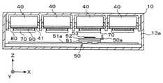
図2及び図3はそれぞれ、本実施形態にかかる検査装置の構成の概略を示す上面横断面図及び正面縦断面図である。 2 and 3 are a top sectional view and a front vertical sectional view showing an outline of the configuration of the inspection device according to the present embodiment, respectively.
図2及び図3の検査装置1は、基板としてのウェハWを検査するものであり、具体的には、ウェハWに形成された検査対象デバイスとしての半導体デバイスの電気的特性検査を行うものである。検査装置1は、筐体10を有し、該筐体10には、搬入出領域11、搬送領域12、検査領域13が設けられている。搬入出領域11は、検査装置1に対してウェハWの搬入出が行われる領域である。搬送領域12は、搬入出領域11と検査領域13とを接続する領域である。また、検査領域13は、ウェハWに形成された半導体デバイスの電気的特性検査が行われる領域である。 The
搬入出領域11には、複数のウェハWを収容したカセットCを受け入れるポート20、後述のプローブカードを収容するローダ21、検査装置1の各構成要素を制御する制御部22が設けられている。制御部22は、例えばCPUやメモリ等を備えたコンピュータにより構成され、プログラム格納部(図示せず)を有している。プログラム格納部には、検査装置1における各種処理を制御するプログラムが格納されている。なお、上記プログラムは、コンピュータに読み取り可能な記憶媒体に記録されていたものであって、当該記憶媒体から制御部22にインストールされたものであってもよい。プログラムの一部または全ては専用ハードウェア(回路基板)で実現してもよい。 The carry-in /
搬送領域12には、ウェハW等を保持した状態で自在に移動可能な搬送装置30が配置されている。この搬送装置30は、搬入出領域11のポート20内のカセットCと、検査領域13との間でウェハWの搬送を行う。また、搬送装置30は、検査領域13内の後述のポゴフレームに固定されたプローブカードのうちメンテナンスを必要とするものを搬入出領域11のローダ21へ搬送する。さらに、搬送装置30は、新規な又はメンテナンス済みのプローブカードをローダ21から検査領域13内の上記ポゴフレームへ搬送する。 In the
検査領域13は、テスタ40が複数設けられている。具体的には、検査領域13は、図3に示すように、鉛直方向に3つに分割され、各分割領域13aには、水平方向(図のX方向)に配列された複数(図の例では4つ)のテスタ40からなるテスタ列が設けられている。また、各分割領域13aには、1つの位置合わせ機構としてのアライナ50と、1つのカメラ60が設けられている。つまり、各分割領域13aでは、1つのアライナ50及び1つのカメラ60が複数のテスタ40に対し共通に用いられる。後述のように、各テスタ40に対して、プローブカードが設けられるため、1つのアライナ50及び1つのカメラ60は複数のプローブカードに対し共通に用いられる。なお、テスタ40、アライナ50、カメラ60の数や配置は任意に選択できる。 A plurality of
テスタ40は、電気的特性検査用の電気信号をウェハWとの間で送受するものである。
アライナ50は、ウェハWが載置される載置部材としてのチャックトップ70を保持して、左右方向(図2のX方向)、前後方向(図2のY方向)及び上下方向(図2のZ方向)移動させるものである。このアライナ50により、チャックトップ70に載置されたウェハWと後述のプローブカードのプローブとの位置合わせを行うことができる。なお、アライナ50には、後述のプローブカードを撮像するカメラ50aが設けられている。The
The
カメラ60は、水平に移動し、当該カメラ60が設けられた分割領域13a内の各テスタ40の前に位置して、アライナ50上のチャックトップ70に載置されたウェハWを撮像する。
カメラ60の撮像結果とアライナ50に設けられたカメラ50aの撮像結果は、プローブカードのプローブとチャックトップ70上のウェハWに形成された半導体デバイスの電極との位置合わせに用いられる。The
The image pickup result of the
チャックトップ70は、載置されたウェハWを吸着等により保持することができる。 The
この検査装置1では、搬送装置30が一のテスタ40へ向けてウェハWを搬送している間に、他のテスタ40は他のウェハWに形成された電子デバイスの電気的特性の検査を行うことができる。 In this
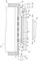
続いて、図4及び図5を用いて、アライナ50の構成及びテスタ40の周囲の構成について説明する。図4は、各分割領域13a内の構成を示す正面縦断面図である。図5は、図4の部分拡大図である。 Subsequently, the configuration of the
アライナ50は、図4に示すように、例えばXステージ51、Yステージ52及びZステージ53を有する。Xステージ51は、ガイドレール51aに沿って左右方向(図4のX方向)に移動する。Yステージ52は、Xステージ51上を前後方向(図4のY方向)に移動する。Zステージ53は、Yステージ52に対し上下方向(図4のZ方向)に移動する。また、このZステージ53上にチャックトップ70が着脱自在に吸着保持される。Zステージ53によるチャックトップ70の吸着保持は、吸着保持機構(図示せず)による真空吸着等により行われる。 As shown in FIG. 4, the
上述のような構成により、アライナ50は、ウェハWが載置されたチャックトップ70を保持して、左右方向(図4のX方向)、前後方向(図4のY方向)及び上下方向(図4のZ方向)移動させることができる。 With the above configuration, the
また、アライナ50のZステージ53には、図5に示すように、変位センサ53aが複数設けられている。変位センサ53aは、例えば、チャックトップ70に対するアライナ50の位置を検出するためのセンサとして用いられる。この変位センサ53aは、アライナ50とチャックトップ70との距離を検出する。具体的には、変位センサ53aは、アライナ50のZステージ53の上面すなわちチャックトップ70を保持する面とチャックトップ70の下面との距離を検出する。 Further, as shown in FIG. 5, a plurality of
さらに、アライナ50には、当該アライナ50とチャックトップ70との相対的な傾きを調整する傾き調整機構(図示せず)が設けられている。 Further, the
なお、アライナ50は、制御部22により制御され、また、変位センサ53aによる検出結果は制御部22に出力される。 The
テスタ40は、図5に示すように、水平に設けられたテスタマザーボード41を底部に有する。テスタマザーボード41には、複数の検査回路基板(図示せず)が立設状態で装着されている。また、テスタマザーボード41の底面には複数の電極(図示せず)が設けられている。
さらに、テスタ40の下方には、ポゴフレーム80とプローブカード90とがそれぞれ1つずつ上側からこの順で設けられている。As shown in FIG. 5, the
Further, below the
ポゴフレーム80は、プローブカード90を支持すると共に、当該プローブカード90とテスタ40とを電気的に接続するものであり、テスタ40とプローブカード90との間に位置するように配設されている。このポゴフレーム80は、テスタ40とプローブカード90とを電気的に接続するポゴピン81を有し、具体的には、多数のポゴピン81を保持するポゴブロック82を有する。また、ポゴフレーム80は、ポゴブロック82が挿篏されることによりポゴピン81が取り付けられる取り付け孔83aが形成されたフレーム本体83を有する。 The
ポゴフレーム80の下面には、プローブカード90が、所定の位置に位置合わせされた状態で支持される。 A
なお、排気機構(図示せず)によって、テスタマザーボード41はポゴフレーム80に真空吸着され、プローブカード90は、ポゴフレーム80に真空吸着される。これら真空吸着を行うための真空吸引力により、ポゴフレーム80の各ポゴピン81の下端は、プローブカード90の後述のカード本体91の上面における、対応する電極パッドに接触し、各ポゴピン81の上端は、テスタマザーボード41の下面の対応する電極に押し付けられる。 By the exhaust mechanism (not shown), the
プローブカード90は、複数の電極パッドが上面に設けられた円板状のカード本体91を有する。カード本体91の下面には、下方へ向けて延びる針状の接触端子であるプローブ92が複数設けられている。
カード本体91の上面に設けられた上述の複数の電極パッドはそれぞれ対応するプローブ92と電気的に接続されている。また、検査時には、プローブ92はそれぞれ、ウェハWに形成された半導体デバイスの電極と接触する。したがって、電気的特性検査時には、ポゴピン81、カード本体91の上面に設けられた電極パッド及びプローブ92を介して、テスタマザーボード41とウェハW上の半導体デバイスとの間で、検査にかかる電気信号が送受される。
なお、検査装置1は、ウェハWに形成された複数の半導体デバイスの電気的特性検査を一括で行うために、プローブ92は、カード本体91の下面略全体を覆うように多数設けられている。The
The plurality of electrode pads provided on the upper surface of the
The
また、ポゴフレーム80の下面には、筒状部材としてのベローズ84が取り付けられている。ベローズ84は、プローブカード90を囲繞するように垂下する筒状の伸縮自在な部材である。ベローズ84の下端には、環状の当接部84aが設けられている。 Further, a bellows 84 as a tubular member is attached to the lower surface of the
ベローズ84は、プローブカード90の下方の位置に、シール部としてのリップシール100を介してチャックトップ70を吸着保持する。 The bellows 84 attracts and holds the
リップシール100は弾性を有しており、例えば樹脂材料から形成される。リップシール100は、チャックトップ70に載置されたウェハWを囲み、且つ、ベローズ84に対向するように、チャックトップ70の上面に設けられる。リップシール100は、上方に向けて開口しており、ベローズ84の当接部84aと当接する。リップシール100は、リップシール100とベローズ84とで囲まれる封止空間Pを形成する。具体的には、リップシール100は、リップシール100とベローズ84の当接部84aとで囲まれる封止空間Pを形成する。封止空間Pは、チャックトップ70に形成された排気路70aの一端に連通している。排気路70aの他端には、減圧機構110と大気開放機構120とが接続されている。 The
減圧機構110は、封止空間Pを減圧する。これにより、チャックトップ70がリップシール100を介してベローズ84に吸着され保持される。つまり、減圧機構110は、リップシール100を介してチャックトップ70をベローズ84で吸着保持する吸着保持力を生じさせる。減圧機構110は、封止空間Pを排気する真空ポンプや真空ポンプによる排気の開始と停止を切り換える切換弁等を有し、制御部22により制御される。 The
大気開放機構120は、チャックトップ70をベローズ84から取り外すための機構すなわちベローズ84によるチャックトップ70の吸着保持を停止させる機構であり、封止空間Pに大気を導入する。大気開放機構120は、封止空間Pへの大気導入の開始と停止を切り換える切換弁等を有し、制御部22により制御される。
ベローズ84からのチャックトップ70の取り外しのために、大気を導入する代わりに不活性ガス等を導入するようにしてもよい。The
In order to remove the chuck top 70 from the
また、ベローズ84は、リップシール100を介してチャックトップ70を吸着保持することにより、プローブカード90を含むポゴフレーム80、ベローズ84、リップシール100及びチャックトップ70で囲まれる密閉空間Sを形成する。密閉空間Sは、ポゴフレーム80のフレーム本体83に形成された排気路83bの一端に連通している。排気路83bの他端には、減圧機構130と大気開放機構140とが接続されている。 Further, the
減圧機構130は、密閉空間Sを減圧する。これにより、ウェハWとプローブ92との接触状態が維持される。減圧機構130は、密閉空間Sを排気する真空ポンプや真空ポンプによる排気の開始と停止を切り換える切換弁等を有し、制御部22により制御される。 The
大気開放機構140は、密閉空間Sを大気圧に戻すための機構であり、密閉空間Sに大気を導入する。大気開放機構140は、封止空間Pへの大気導入の開始と停止を切り換える切換弁等を有し、制御部22により制御される。
密閉空間Sを大気圧に戻すために、大気を導入する代わりに不活性ガス等を導入するようにしてもよい。The
In order to return the enclosed space S to atmospheric pressure, an inert gas or the like may be introduced instead of introducing the atmosphere.
なお、ポゴフレーム80のフレーム本体83の下面には、ポゴフレーム80に対するチャックトップ70の位置を検出するためのセンサとして変位センサ85が複数設けられている。変位センサ85は、ポゴフレーム80からチャックトップ70までの距離、具体的には、変位センサ85からチャックトップ70の上面までの距離を検出する。変位センサ85による検出結果は制御部22に出力される。 A plurality of
次に検査装置1を用いた検査処理について説明する。 Next, the inspection process using the
(搬入及び位置合わせ)
まず、検査対象のウェハWの搬入と、当該ウェハWとプローブカード90との位置合わせが行われる。
具体的には、搬送装置30等が制御部22により制御され、搬入出領域11のポート20内のカセットCからウェハWが取り出されて、検査領域13内に搬入され、アライナ50に吸着保持されたチャックトップ70上に載置される。次いで、カメラ60でのチャックトップ70上のウェハWの撮像結果とカメラ50aによるプローブ92の撮像結果とに基づいて、アライナ50が、制御部22により制御され、チャックトップ70上のウェハWとプローブ92との水平方向にかかる位置合わせが行われる。(Delivery and alignment)
First, the wafer W to be inspected is carried in, and the wafer W and the
Specifically, the
(チャックトップ70の吸着保持及びプローブ92の押圧接触)
続いて、チャックトップ70をベローズ84に吸着保持させると共に、ウェハWにプローブ92を押圧して接触させる。
具体的には、例えば、チャックトップ70を吸着保持したアライナ50のZステージ53を上昇させることにより、チャックトップ70を上昇させ、ベローズ84の当接部84aとリップシール100とを当接させる。これにより、当接部84aとリップシール100とで囲まれる封止空間Pを形成する。次いで、減圧機構110によって封止空間Pが減圧され、これにより、チャックトップ70がリップシール100を介してベローズ84に吸着保持されると共に、ポゴフレーム80、ベローズ84、リップシール100及びチャックトップ70で囲まれる密閉空間Sが形成される。(Adsorption holding of
Subsequently, the
Specifically, for example, by raising the
その後も、アライナ50のZステージ53の上昇によるチャックトップ70の上昇を継続させ、プローブカード90のプローブ92とウェハWに形成された半導体デバイスの電極とを当接させる。
当接後も、アライナ50のZステージ53の上昇によるチャックトップ70の上昇を継続させ、チャックトップ70上のウェハWの電極にプローブ92を押圧して接触させる。なお、プローブ92とウェハWの電極との当接後にチャックトップ70を上昇させた量を、以下では「オーバードライブ量」という。次いで、減圧機構130によって密閉空間Sが所定の圧力まで減圧され、チャックトップ70がプローブカード90に引きつけられる。After that, the
Even after the contact, the
次いで、アライナ50のZステージ53によるチャックトップ70の吸着保持を解除すると共に、Zステージ53を下降させる。このとき、密閉空間Sが所定の圧力まで減圧されているため、チャックトップ70は、Zステージ53から切り離され、プローブカード90に引きつけられ続け、チャックトップ70上のウェハWの電極にプローブ92が押圧された状態で接触され続ける。このとき、封止空間Pの減圧は継続されている。これにより、密閉空間Sを確実に密閉し続けることができる。 Next, the suction holding of the
(検査)
チャックトップ70とアライナ50のZステージ53との切り離し後、テスタ40からポゴピン81等を介してプローブ92に電気的特性検査用の電気信号が入力され、ウェハWに形成された電子デバイスの電気的特性検査が行われる。(test)
After disconnecting the
(プローブ92の接触の解除及びチャックトップ70の取り外し)
電気的特性検査が完了すると、検査後のウェハWとプローブ92との接触が解除されると共に、検査後のウェハWが載置されたチャックトップ70が、ベローズ84から取り外され、アライナ50に支持される。この工程における、ベローズ84からのチャックトップ70の取り外しを含む、ウェハWとプローブ92との接触を解除する方法(以下、「接触解除・取り外し方法」という。)の詳細については後述する。(Release of contact of
When the electrical characteristic inspection is completed, the contact between the inspected wafer W and the
(搬出)
その後、検査後のウェハWが搬出される。
具体的には、搬送装置30等が制御部22により制御され、アライナ50に保持されたチャックトップ70上の検査後のウェハWが、検査領域13から搬出され、搬入出領域11のポート20内のカセットCに戻される。
なお、一のテスタ40での検査中、アライナ50によって、他のテスタ40への検査対象のウェハWの搬送や他のテスタ40からの検査後のウェハWの回収が行われる。(Carrying out)
After that, the inspected wafer W is carried out.
Specifically, the
During the inspection by one
次に、上述の接触解除・取り外し方法について図6及び図7を用いて説明する。図6は、上記接触解除・取り外し方法の一例を説明するためのフローチャートであり、図7は、当該方法の各工程でのチャックトップ70やアライナ50等の状態を示す図である。 Next, the above-mentioned contact release / removal method will be described with reference to FIGS. 6 and 7. FIG. 6 is a flowchart for explaining an example of the contact release / removal method, and FIG. 7 is a diagram showing a state of the
本例では、変位センサ53aによる検出結果が用いられるところ、まず、変位センサ53aによる検出値の較正が行われる(ステップS1)。
具体的には、まず、アライナ50のZステージ53を、ベローズ84に支持されたチャックトップ70の下方の空間に、Xステージ51及びYステージ52によって移動させた後、所定量Δh(例えば100μm)上昇させる。この上昇前後で、アライナ50のZステージ53の上面からチャックトップ70の下面までの距離を変位センサ53aで検出しておき、これら検出結果と、Zステージ53の上昇量すなわち上記所定量Δhとに基づいて、制御部22が、変位センサ53aによる検出値を較正する。変位センサ53aは複数設けられており、上述の較正は変位センサ53a毎に行われる。In this example, where the detection result by the
Specifically, first, the
続いて、アライナ50とチャックトップ70とが相対的に傾いているか否かの判定が行われる(ステップS2)。
具体的には、例えば、制御部22が、アライナ50のZステージ53の上面からチャックトップ70の下面までの距離を複数の変位センサ53aに検出させ、これら検出結果に基づいて、アライナ50のZステージ53とチャックトップ70との相対的な傾きを算出する。そして、制御部22が、算出した上記相対的なの傾きが所定値を超えているか否か判定する。
判定の結果、所定値を超えている場合、すなわち、アライナ50とチャックトップ70とが相対的に傾いている場合(YESの場合)、アライナ50に設けられた傾き調整機構(図示せず)を用いてアライナ50とチャックトップ70との相対的な傾きの調整が行われる(ステップS3)。なお、算出された傾きが所定値を超えていない場合、すなわち、アライナ50とチャックトップ70とが相対的に傾いていない場合(NOの場合)は、ステップS3の傾き調整工程は省略される。Subsequently, it is determined whether or not the
Specifically, for example, the
As a result of the determination, when the predetermined value is exceeded, that is, when the
次に、図7(A)に示すように、アライナ50を、予め定められた開放位置まで上昇させ、密閉空間Sを形成しているチャックトップ70に近づける(ステップS4)。
具体的には、アライナ50のZステージ53を上記開放位置まで徐々に上昇させ、Zステージ53の上面を、密閉空間Sを形成しているチャックトップ70の下面に徐々に近づける。上記開放位置は、例えば、変位センサ53aによって検出される、アライナ50のZステージ53の上面からチャックトップ70の下面までの距離Lが、前述のオーバードライブ量OD未満となる位置であり、より具体的には、上記距離Lが60μm以下となる位置であり、より好ましくは、上記距離Lが30μm以下となる位置である。Next, as shown in FIG. 7A, the
Specifically, the
続いて、アライナ50によるチャックトップ70の吸着動作を開始させる(ステップS5)。
具体的には、制御部22が、アライナ50に対し設けられた吸着保持機構(図示せず)を制御し、アライナ50のZステージ53によるチャックトップ70の吸着動作を開始させる。ただし、この時点においては、チャックトップ70は、Zステージ53から離間しているため、実際にはZステージ53には吸着保持されない。Subsequently, the suction operation of the
Specifically, the
次に、密閉空間Sの減圧を停止すると共に密閉空間Sを大気圧に戻す(ステップS6)。
具体的には、制御部22が、減圧機構110及び大気開放機構120を制御し、プローブカード90を含むポゴフレーム80、ベローズ84、リップシール100及びチャックトップ70で囲まれる密閉空間Sの減圧を停止し、当該密閉空間Sを排気路83bを介して大気開放する。
このとき、チャックトップ70及びチャックトップ70に載置されているウェハWは、ウェハWに押圧されているプローブ92の反力及び自重により、図7(B)に示すように、下降する。ただし、アライナ50のZステージ53が上記開放位置に位置するため、密閉空間Sを大気開放しても、ウェハWに対するプローブ92の押圧された状態での接触が解除されない程度に、Zステージ53とチャックトップ70とが近接している。したがって、密閉空間Sを大気開放することによって、チャックトップ70の中心周りのモーメントがチャックトップ70に生じても、チャックトップ70は大きく傾かずに、Zステージ53に支持される。Next, the depressurization of the closed space S is stopped and the closed space S is returned to the atmospheric pressure (step S6).
Specifically, the
At this time, the wafer W placed on the
チャックトップ70は、Zステージ53に支持されると、上述のように吸着動作が既に開始されているため、Zステージ53に吸着保持される。なお、チャックトップ70は、ベローズ84にもリップシール100を介して引き続き吸着保持されている。 When the
続いて、チャックトップ70を吸着保持したアライナ50のZステージ53を下降させ、図7(C)に示すように、ウェハWとプローブ92との押圧された状態での接触を解除する(ステップS7)。
このとき、Zステージ53の下降量は、少なくともオーバードライブ量OD以上であり、例えば200〜500μmである。これにより、ウェハWとプローブ92との押圧された状態での接触を確実に解除することができ、より具体的には、ウェハWとプローブ92とを確実に離間させることができる。
なお、この工程におけるZステージ53の下降量は、プローブカード90の反り等を考慮して設定することが好ましい。Subsequently, the
At this time, the amount of descent of the
The amount of descent of the
次に、リップシール100を介したベローズ84によるチャックトップ70の吸着保持が停止され、図7(D)に示すように、チャックトップ70がベローズ84から取り外される(ステップS8)。
具体的には、制御部22が、減圧機構130及び大気開放機構140を制御し、リップシール100とベローズ84とで囲まれる封止空間Pの減圧を停止させると共に、排気路70aを介して封止空間Pを大気圧に戻す。これにより、リップシール100を介したベローズ84によるチャックトップ70の吸着保持が解除され、チャックトップ70が、ベローズ84から取り外され、アライナ50のZステージ53のみで支持される。
そして、制御部22が、アライナ50のZステージ53を所定の位置まで下降させる。Next, the suction and holding of the
Specifically, the
Then, the
リップシール100を介したベローズ84によるチャックトップ70の吸着保持が解除されると、当該吸着保持時に変形していたリップシール100からの反力により、チャックトップ70が水平方向に移動すること、すなわち、水平方向にずれることがある。このように水平方向にずれが生じたとしても、ステップS7によりウェハWとプローブ92とが離間しているため、プローブ92がウェハW上を摺動することがない。したがって、リップシール100からの反力に起因して、ウェハW上にプローブ92による長い接触痕が形成されることがない。 When the suction holding of the
次に、チャックトップ70を吸着保持したアライナ50のZステージ53の下降がさらに行われる(ステップS9)。 Next, the
その後、チャックトップ70の位置をリセットするか否かの判定が行われる(ステップS10)。
具体的には、例えば、制御部22が、複数の変位センサ53aでの検出結果に基づいて、アライナ50のZステージ53に保持されたチャックトップ70の、Zステージ53に対する傾きを算出し、算出したチャックトップ70の傾きが所定値を超えているか否か判定する。
判定の結果、所定値を超えている場合、すなわち、チャックトップ70がZステージ53における所望の位置に載置されておらず傾いている場合(YESの場合)、チャックトップ70の位置のリセット動作が行われる(ステップS11)。上記リセット動作は、例えば、Xステージ51及びYステージ52の少なくともいずれか一方を振動させる動作である。なお、算出されたチャックトップ70の傾きが所定値を超えていない場合、すなわち、チャックトップ70が傾いていない場合(NOの場合)は、ステップS11のリセット工程は省略される。After that, it is determined whether or not to reset the position of the chuck top 70 (step S10).
Specifically, for example, the
As a result of the determination, when the predetermined value is exceeded, that is, when the
以上のように、本実施形態にかかる、プローブ92とウェハWとの接触の解除方法は、アライナ50を予め定められた解除位置まで上昇させ、密閉空間Sを形成しベローズ84に吸着保持されているチャックトップ70に近づける工程と、その後、密閉空間Sの減圧を停止し、ウェハWに対するプローブ92の押圧された状態での接触が解除されないように、上記解除位置のアライナ50でチャックトップ70を支持する工程と、を含む。そのため、密閉空間Sを大気開放することによって、チャックトップ70の中心周りのモーメントがチャックトップ70に生じても、チャックトップ70は大きく傾かずに、Zステージ53に支持される。したがって、密閉空間Sを大気開放したときに、プローブ92が相対的にチャックトップ70に保持されたウェハWの上面に沿って大きく移動することがない。つまり、密閉空間Sを開放したときに、ウェハWにプローブ92による長い接触痕が形成されることがない。 As described above, in the method for releasing the contact between the
また、本実施形態にかかる方法は、アライナ50でチャックトップ70を支持する工程後、チャックトップ70を吸着保持したアライナ50を下降させ、ウェハWに対するプローブ92の押圧された状態での接触を解除する工程と、その後、リップシール100を介したベローズ84によるチャックトップ70の吸着保持を停止する工程と、を含む。すなわち、本実施形態にかかる方法では、ウェハWとプローブ92とが離間された状態で、リップシール100を介したベローズ84によるチャックトップ70の吸着保持が解除される。そのため、上記吸着保持を解除したときに、リップシール100の反力により、プローブ92に対しチャックトップ70が水平方向にずれても、チャックトップ70に載置されているウェハWに、プローブ92による長い接触痕が形成されることがない。 Further, in the method according to the present embodiment, after the step of supporting the
このように、本実施形態によれば、ウェハWとプローブとの接触を解除するときに長い接触痕が生じるのを防ぐことができる。また、このように防止するためにプローブ502aのウェハWへの押圧力を低下させる必要がない。 As described above, according to the present embodiment, it is possible to prevent long contact marks from being generated when the contact between the wafer W and the probe is released. Further, in order to prevent this, it is not necessary to reduce the pressing force of the
以上の例では、ステップS4において、アライナ50を開放位置まで徐々に上昇させており、また、変位センサ53aによって検出される、アライナ50のZステージ53の上面からチャックトップ70の下面までの距離Lが予め定められた値以下となる位置を、上記開放位置としている。これに代えて、例えば、ステップS4において、アライナ50を開放位置まで段階的に上昇させ、一段階での上昇量に比べ、変位センサで検出される上記距離Lの変化量が小さくなる位置を、上記開放位置としてもよい。また、ステップS4において、アライナ50を開放位置まで徐々に上昇させる際、変位センサ85で検出される、ポゴフレーム80からチャックトップ70までの距離に変化(例えば数μmの変化)が生じた位置を、上記開放位置としてもよい。 In the above example, in step S4, the
また、以上の例では、リップシール100はチャックトップ70の上面に設けられていた。リップシールは、ベローズ84の当接部84aの下面に設けられていてもよい。この場合も、リップシールと当該リップシールが接触するチャックトップ70の上面とで囲まれる封止空間を減圧することにより、リップシールを介してチャックトップ70をベローズ84で吸着保持することができる。 Further, in the above example, the
なお、以上の例では、リップシール100を介したベローズ84によるチャックトップ70の吸着保持を真空吸着により行っていた。これに代えて、例えば、ベローズ84の当接部84aとチャックトップ70の上面との静電吸着により、上記吸着保持を行うようにしてもよい。 In the above example, the suction and holding of the
今回開示された実施形態はすべての点で例示であって制限的なものではないと考えられるべきである。上記の実施形態は、添付の請求の範囲及びその主旨を逸脱することなく、様々な形態で省略、置換、変更されてもよい。 The embodiments disclosed this time should be considered to be exemplary and not restrictive in all respects. The above embodiments may be omitted, replaced or modified in various forms without departing from the scope of the appended claims and their gist.
1 検査装置
22 制御部
50 アライナ
70 チャックトップ
84 ベローズ
90 プローブカード
92 プローブ
100 リップシール
110 減圧機構
130 減圧機構
S 密閉空間
W ウェハ1
Claims (7)
Translated fromJapanese前記検査装置は、
基板が載置される板状の載置部材と、
前記載置部材を保持し移動させ、前記載置部材に載置された基板と前記プローブとの位置合わせを行うように構成された位置合わせ機構と、
前記プローブが複数設けられたプローブカードを囲繞するように垂下する筒状の伸縮自在な筒状部材と、を備え、
基板に対し前記プローブが押圧されて接触した状態で、前記載置部材、前記筒状部材及び前記プローブカードで囲まれる検査空間が減圧され、且つ、弾性を有するシール部を介して前記載置部材が前記筒状部材に吸着保持され、
当該方法は、
前記位置合わせ機構を予め定められた位置まで上昇させ、前記検査空間を形成している前記載置部材に近づける工程と、
その後、前記検査空間の減圧を停止し、前記プローブの、基板に対する押圧された状態での接触が解除されないように、前記予め定められた位置の前記位置合わせ機構で前記載置部材を支持する工程と、
その後、前記載置部材を保持した前記位置合わせ機構を下降させ、前記プローブの、基板に対する押圧された状態での接触を解除する工程と、
その後、前記シール部を介した前記筒状部材による前記載置部材の吸着保持を停止する工程と、を含む、接触解除方法。It is a method of breaking the contact between the inspection probe and the substrate in the inspection device for inspecting the substrate.
The inspection device is
A plate-shaped mounting member on which the substrate is mounted, and
An alignment mechanism configured to hold and move the previously described mounting member to align the substrate mounted on the previously described mounting member with the probe.
A cylindrical telescopic tubular member that hangs down so as to surround a probe card provided with a plurality of the probes is provided.
In a state where the probe is pressed against the substrate and is in contact with the substrate, the inspection space surrounded by the previously described member, the tubular member, and the probe card is decompressed, and the previously described member is placed through an elastic seal portion. Is adsorbed and held by the tubular member,
The method is
A step of raising the alignment mechanism to a predetermined position and bringing it closer to the previously described placing member forming the inspection space.
After that, the step of stopping the depressurization of the inspection space and supporting the above-mentioned placement member by the alignment mechanism at the predetermined position so that the contact of the probe with respect to the substrate in a pressed state is not released. When,
After that, the step of lowering the alignment mechanism holding the above-mentioned mounting member to release the contact of the probe with respect to the substrate in a pressed state, and
A method for releasing contact, comprising a step of stopping the suction and holding of the previously described member by the tubular member via the seal portion.
前記予め定められた位置は、前記位置合わせ機構から前記載置部材までの距離が、前記プローブと基板とが当接した後に前記載置部材を上昇させた量未満となる位置である、請求項1〜5のいずれか1項に記載の接触解除方法。In the alignment mechanism, when the probe is raised to bring the probe into contact with the substrate, the probe and the substrate are brought into contact with each other, and then the preceding member is further raised.
The predetermined position is a position where the distance from the alignment mechanism to the previously described member is less than the amount by which the previously described member is raised after the probe and the substrate come into contact with each other. The contact release method according to any one of 1 to 5.
基板が載置される板状の載置部材と、
前記載置部材を保持し移動させ、前記載置部材に載置された基板と検査用のプローブとの位置合わせを行うように構成された位置合わせ機構と、
前記プローブが複数設けられたプローブカードを囲繞するように垂下する筒状の伸縮自在な筒状部材と、
前記載置部材、前記筒状部材及び前記プローブカードで囲まれる検査空間を減圧する減圧機構と、
弾性を有するシール部を介して前記載置部材を前記筒状部材で吸着保持する吸着保持力を生じる吸着保持機構と、
制御部と、を備え、
前記制御部は、
基板に対し前記プローブが押圧されて接触した状態で前記検査空間が減圧され前記載置部材が前記シール部を介して前記筒状部材に吸着保持されているときに、前記位置合わせ機構を予め定められた位置まで上昇させ、前記検査空間を形成している前記載置部材に近づける工程と、
その後、前記検査空間の減圧を停止し、前記プローブの、基板に対する押圧された状態での接触が解除されないように、前記予め定められた位置の前記位置合わせ機構で前記載置部材を支持する工程と、
その後、前記載置部材を保持した前記位置合わせ機構を下降させ、前記プローブの、基板に対する押圧された状態での接触を解除する工程と、
その後、前記シール部を介した前記筒状部材による前記載置部材の吸着保持を停止する工程と、が実行されるよう制御信号を出力する、検査装置。
An inspection device that inspects the board
A plate-shaped mounting member on which the substrate is mounted, and
An alignment mechanism configured to hold and move the previously described mounting member to align the substrate mounted on the previously described mounting member with the inspection probe.
A tubular member that hangs down so as to surround a probe card provided with a plurality of probes, and a tubular member that can be expanded and contracted.
A decompression mechanism for reducing the pressure in the inspection space surrounded by the above-mentioned mounting member, the tubular member, and the probe card,
A suction holding mechanism that generates a suction holding force that sucks and holds the previously described member with the tubular member via an elastic sealing portion.
With a control unit,
The control unit
The alignment mechanism is predetermined when the inspection space is decompressed and the previously described member is adsorbed and held by the tubular member via the seal portion in a state where the probe is pressed against the substrate and is in contact with the substrate. The process of raising the inspection space to the designated position and bringing it closer to the previously described mounting member forming the inspection space.
After that, the step of stopping the depressurization of the inspection space and supporting the above-mentioned placement member by the alignment mechanism at the predetermined position so that the contact of the probe with respect to the substrate in a pressed state is not released. When,
After that, the step of lowering the alignment mechanism holding the above-mentioned mounting member to release the contact of the probe with respect to the substrate in a pressed state, and
After that, an inspection device that outputs a control signal so that the step of stopping the suction and holding of the previously described member by the tubular member via the seal portion is executed.
Priority Applications (4)
| Application Number | Priority Date | Filing Date | Title |
|---|---|---|---|
| JP2020106054AJP7485552B2 (en) | 2020-06-19 | 2020-06-19 | Contact release method for inspection device and inspection device |
| KR1020210073891AKR102604346B1 (en) | 2020-06-19 | 2021-06-08 | Contact release method in inspection apparatus and inspection apparatus |
| CN202110642553.7ACN113823577B (en) | 2020-06-19 | 2021-06-09 | Contact releasing method in inspection device and inspection device |
| US17/347,325US11467208B2 (en) | 2020-06-19 | 2021-06-14 | Contact release method in inspection apparatus and inspection apparatus |
Applications Claiming Priority (1)
| Application Number | Priority Date | Filing Date | Title |
|---|---|---|---|
| JP2020106054AJP7485552B2 (en) | 2020-06-19 | 2020-06-19 | Contact release method for inspection device and inspection device |
Publications (2)
| Publication Number | Publication Date |
|---|---|
| JP2022000878Atrue JP2022000878A (en) | 2022-01-04 |
| JP7485552B2 JP7485552B2 (en) | 2024-05-16 |
Family
ID=78912522
Family Applications (1)
| Application Number | Title | Priority Date | Filing Date |
|---|---|---|---|
| JP2020106054AActiveJP7485552B2 (en) | 2020-06-19 | 2020-06-19 | Contact release method for inspection device and inspection device |
Country Status (4)
| Country | Link |
|---|---|
| US (1) | US11467208B2 (en) |
| JP (1) | JP7485552B2 (en) |
| KR (1) | KR102604346B1 (en) |
| CN (1) | CN113823577B (en) |
Families Citing this family (1)
| Publication number | Priority date | Publication date | Assignee | Title |
|---|---|---|---|---|
| CN117199895B (en)* | 2023-11-06 | 2024-01-26 | 河南溪亭电力设备有限公司 | Wiring mechanism for mutual inductor detection |
Citations (2)
| Publication number | Priority date | Publication date | Assignee | Title |
|---|---|---|---|---|
| JP2016058506A (en)* | 2014-09-09 | 2016-04-21 | 東京エレクトロン株式会社 | Pressure set point determination method for inspection in wafer inspection device |
| JP2017183423A (en)* | 2016-03-29 | 2017-10-05 | 株式会社東京精密 | Prober and probe contact method |
Family Cites Families (13)
| Publication number | Priority date | Publication date | Assignee | Title |
|---|---|---|---|---|
| KR20040076114A (en)* | 2003-02-24 | 2004-08-31 | 삼성전자주식회사 | Probe needle for probe card |
| JP4156968B2 (en)* | 2003-04-25 | 2008-09-24 | 株式会社オクテック | Probe apparatus and alignment method |
| JP2009099630A (en)* | 2007-10-12 | 2009-05-07 | Japan Electronic Materials Corp | Semiconductor inspection equipment |
| JP5317330B2 (en)* | 2008-09-02 | 2013-10-16 | ルネサスエレクトロニクス株式会社 | Manufacturing method of semiconductor integrated circuit device |
| JP5789206B2 (en)* | 2011-12-08 | 2015-10-07 | 東京エレクトロン株式会社 | Wafer inspection interface and wafer inspection apparatus |
| JP6099347B2 (en) | 2012-10-03 | 2017-03-22 | 東京エレクトロン株式会社 | Wafer mounting method and wafer inspection apparatus |
| JP5571224B2 (en)* | 2013-04-25 | 2014-08-13 | 東京エレクトロン株式会社 | Needle tip position detection device and probe device |
| JP6333112B2 (en)* | 2014-08-20 | 2018-05-30 | 東京エレクトロン株式会社 | Wafer inspection equipment |
| WO2017014060A1 (en)* | 2015-07-23 | 2017-01-26 | 株式会社東京精密 | Prober and probe contact method |
| JP6655514B2 (en)* | 2016-09-21 | 2020-02-26 | 東京エレクトロン株式会社 | Substrate inspection method and substrate inspection device |
| JP6655516B2 (en)* | 2016-09-23 | 2020-02-26 | 東京エレクトロン株式会社 | Board inspection equipment |
| JP6823986B2 (en)* | 2016-09-28 | 2021-02-03 | 東京エレクトロン株式会社 | Board inspection equipment and board inspection method |
| JP6895772B2 (en)* | 2017-03-07 | 2021-06-30 | 東京エレクトロン株式会社 | Inspection equipment and contact method |
- 2020
- 2020-06-19JPJP2020106054Apatent/JP7485552B2/enactiveActive
- 2021
- 2021-06-08KRKR1020210073891Apatent/KR102604346B1/enactiveActive
- 2021-06-09CNCN202110642553.7Apatent/CN113823577B/enactiveActive
- 2021-06-14USUS17/347,325patent/US11467208B2/enactiveActive
Patent Citations (2)
| Publication number | Priority date | Publication date | Assignee | Title |
|---|---|---|---|---|
| JP2016058506A (en)* | 2014-09-09 | 2016-04-21 | 東京エレクトロン株式会社 | Pressure set point determination method for inspection in wafer inspection device |
| JP2017183423A (en)* | 2016-03-29 | 2017-10-05 | 株式会社東京精密 | Prober and probe contact method |
Also Published As
| Publication number | Publication date |
|---|---|
| CN113823577A (en) | 2021-12-21 |
| KR20210157324A (en) | 2021-12-28 |
| KR102604346B1 (en) | 2023-11-20 |
| JP7485552B2 (en) | 2024-05-16 |
| CN113823577B (en) | 2024-01-05 |
| US20210396803A1 (en) | 2021-12-23 |
| US11467208B2 (en) | 2022-10-11 |
Similar Documents
| Publication | Publication Date | Title |
|---|---|---|
| KR102282694B1 (en) | Inspection devices and contact methods | |
| JP6031292B2 (en) | Board contact method to probe card | |
| KR102479608B1 (en) | Contact accuracy assurance method, contact accuracy assurance mechanism, and inspection device | |
| JP7153556B2 (en) | Temperature measurement member, inspection device and temperature measurement method | |
| TW201625969A (en) | Method for determining set value of pressure for inspection in wafer inspection apparatus | |
| CN109863414B (en) | Substrate inspection apparatus and substrate inspection method | |
| JP2016032110A (en) | Probing device and probe contact method | |
| WO2018225384A1 (en) | Inspection apparatus, inspection system, and aligning method | |
| KR102796484B1 (en) | Inspection apparatus and inspection method | |
| WO2018056022A1 (en) | Substrate inspection method and substrate inspection device | |
| JP2022000878A (en) | Contact release method in inspection device and inspection device | |
| CN111446183A (en) | Chuck top, inspection device and method for recovering chuck top | |
| JP7267058B2 (en) | inspection equipment | |
| JP2002076073A (en) | Apparatus and method for testing wafer | |
| JP2021038999A (en) | Electric connection device, inspection device, and electric connection method between contact object and contact piece | |
| JP2021097086A (en) | Prober and probe inspection method | |
| JP7597462B2 (en) | Substrate holding mechanism and substrate mounting method | |
| JP7737852B2 (en) | Inspection device and inspection method |
Legal Events
| Date | Code | Title | Description |
|---|---|---|---|
| A621 | Written request for application examination | Free format text:JAPANESE INTERMEDIATE CODE: A621 Effective date:20230206 | |
| A977 | Report on retrieval | Free format text:JAPANESE INTERMEDIATE CODE: A971007 Effective date:20231109 | |
| A131 | Notification of reasons for refusal | Free format text:JAPANESE INTERMEDIATE CODE: A131 Effective date:20231212 | |
| A521 | Request for written amendment filed | Free format text:JAPANESE INTERMEDIATE CODE: A523 Effective date:20240111 | |
| TRDD | Decision of grant or rejection written | ||
| A01 | Written decision to grant a patent or to grant a registration (utility model) | Free format text:JAPANESE INTERMEDIATE CODE: A01 Effective date:20240409 | |
| A61 | First payment of annual fees (during grant procedure) | Free format text:JAPANESE INTERMEDIATE CODE: A61 Effective date:20240502 | |
| R150 | Certificate of patent or registration of utility model | Ref document number:7485552 Country of ref document:JP Free format text:JAPANESE INTERMEDIATE CODE: R150 |