JP2021511750A - Methods and equipment for packaging ultrasonic on-chips - Google Patents
Methods and equipment for packaging ultrasonic on-chipsDownload PDFInfo
- Publication number
- JP2021511750A JP2021511750AJP2020540804AJP2020540804AJP2021511750AJP 2021511750 AJP2021511750 AJP 2021511750AJP 2020540804 AJP2020540804 AJP 2020540804AJP 2020540804 AJP2020540804 AJP 2020540804AJP 2021511750 AJP2021511750 AJP 2021511750A
- Authority
- JP
- Japan
- Prior art keywords
- ultrasonic
- chip
- interposer
- pcb
- heat sink
- Prior art date
- Legal status (The legal status is an assumption and is not a legal conclusion. Google has not performed a legal analysis and makes no representation as to the accuracy of the status listed.)
- Pending
Links
Images


Classifications
- A—HUMAN NECESSITIES
- A61—MEDICAL OR VETERINARY SCIENCE; HYGIENE
- A61B—DIAGNOSIS; SURGERY; IDENTIFICATION
- A61B8/00—Diagnosis using ultrasonic, sonic or infrasonic waves
- A61B8/44—Constructional features of the ultrasonic, sonic or infrasonic diagnostic device
- A61B8/4483—Constructional features of the ultrasonic, sonic or infrasonic diagnostic device characterised by features of the ultrasound transducer
- A61B8/4494—Constructional features of the ultrasonic, sonic or infrasonic diagnostic device characterised by features of the ultrasound transducer characterised by the arrangement of the transducer elements
- A—HUMAN NECESSITIES
- A61—MEDICAL OR VETERINARY SCIENCE; HYGIENE
- A61B—DIAGNOSIS; SURGERY; IDENTIFICATION
- A61B8/00—Diagnosis using ultrasonic, sonic or infrasonic waves
- A61B8/54—Control of the diagnostic device
- A61B8/546—Control of the diagnostic device involving monitoring or regulation of device temperature
- A—HUMAN NECESSITIES
- A61—MEDICAL OR VETERINARY SCIENCE; HYGIENE
- A61B—DIAGNOSIS; SURGERY; IDENTIFICATION
- A61B8/00—Diagnosis using ultrasonic, sonic or infrasonic waves
- A61B8/56—Details of data transmission or power supply
- B—PERFORMING OPERATIONS; TRANSPORTING
- B06—GENERATING OR TRANSMITTING MECHANICAL VIBRATIONS IN GENERAL
- B06B—METHODS OR APPARATUS FOR GENERATING OR TRANSMITTING MECHANICAL VIBRATIONS OF INFRASONIC, SONIC, OR ULTRASONIC FREQUENCY, e.g. FOR PERFORMING MECHANICAL WORK IN GENERAL
- B06B1/00—Methods or apparatus for generating mechanical vibrations of infrasonic, sonic, or ultrasonic frequency
- B06B1/02—Methods or apparatus for generating mechanical vibrations of infrasonic, sonic, or ultrasonic frequency making use of electrical energy
- B06B1/0292—Electrostatic transducers, e.g. electret-type
- B—PERFORMING OPERATIONS; TRANSPORTING
- B06—GENERATING OR TRANSMITTING MECHANICAL VIBRATIONS IN GENERAL
- B06B—METHODS OR APPARATUS FOR GENERATING OR TRANSMITTING MECHANICAL VIBRATIONS OF INFRASONIC, SONIC, OR ULTRASONIC FREQUENCY, e.g. FOR PERFORMING MECHANICAL WORK IN GENERAL
- B06B1/00—Methods or apparatus for generating mechanical vibrations of infrasonic, sonic, or ultrasonic frequency
- B06B1/02—Methods or apparatus for generating mechanical vibrations of infrasonic, sonic, or ultrasonic frequency making use of electrical energy
- B06B1/06—Methods or apparatus for generating mechanical vibrations of infrasonic, sonic, or ultrasonic frequency making use of electrical energy operating with piezoelectric effect or with electrostriction
- B06B1/0607—Methods or apparatus for generating mechanical vibrations of infrasonic, sonic, or ultrasonic frequency making use of electrical energy operating with piezoelectric effect or with electrostriction using multiple elements
- B06B1/0622—Methods or apparatus for generating mechanical vibrations of infrasonic, sonic, or ultrasonic frequency making use of electrical energy operating with piezoelectric effect or with electrostriction using multiple elements on one surface
- B—PERFORMING OPERATIONS; TRANSPORTING
- B81—MICROSTRUCTURAL TECHNOLOGY
- B81B—MICROSTRUCTURAL DEVICES OR SYSTEMS, e.g. MICROMECHANICAL DEVICES
- B81B7/00—Microstructural systems; Auxiliary parts of microstructural devices or systems
- B81B7/0032—Packages or encapsulation
- B81B7/0045—Packages or encapsulation for reducing stress inside of the package structure
- B81B7/0048—Packages or encapsulation for reducing stress inside of the package structure between the MEMS die and the substrate
- B—PERFORMING OPERATIONS; TRANSPORTING
- B81—MICROSTRUCTURAL TECHNOLOGY
- B81C—PROCESSES OR APPARATUS SPECIALLY ADAPTED FOR THE MANUFACTURE OR TREATMENT OF MICROSTRUCTURAL DEVICES OR SYSTEMS
- B81C1/00—Manufacture or treatment of devices or systems in or on a substrate
- B81C1/00015—Manufacture or treatment of devices or systems in or on a substrate for manufacturing microsystems
- B81C1/00261—Processes for packaging MEMS devices
- G—PHYSICS
- G01—MEASURING; TESTING
- G01N—INVESTIGATING OR ANALYSING MATERIALS BY DETERMINING THEIR CHEMICAL OR PHYSICAL PROPERTIES
- G01N29/00—Investigating or analysing materials by the use of ultrasonic, sonic or infrasonic waves; Visualisation of the interior of objects by transmitting ultrasonic or sonic waves through the object
- G01N29/04—Analysing solids
- G01N29/06—Visualisation of the interior, e.g. acoustic microscopy
- G01N29/0654—Imaging
- H—ELECTRICITY
- H10—SEMICONDUCTOR DEVICES; ELECTRIC SOLID-STATE DEVICES NOT OTHERWISE PROVIDED FOR
- H10N—ELECTRIC SOLID-STATE DEVICES NOT OTHERWISE PROVIDED FOR
- H10N39/00—Integrated devices, or assemblies of multiple devices, comprising at least one piezoelectric, electrostrictive or magnetostrictive element covered by groups H10N30/00 – H10N35/00
- A—HUMAN NECESSITIES
- A61—MEDICAL OR VETERINARY SCIENCE; HYGIENE
- A61B—DIAGNOSIS; SURGERY; IDENTIFICATION
- A61B2562/00—Details of sensors; Constructional details of sensor housings or probes; Accessories for sensors
- A61B2562/16—Details of sensor housings or probes; Details of structural supports for sensors
- A61B2562/166—Details of sensor housings or probes; Details of structural supports for sensors the sensor is mounted on a specially adapted printed circuit board
- A—HUMAN NECESSITIES
- A61—MEDICAL OR VETERINARY SCIENCE; HYGIENE
- A61B—DIAGNOSIS; SURGERY; IDENTIFICATION
- A61B2562/00—Details of sensors; Constructional details of sensor housings or probes; Accessories for sensors
- A61B2562/22—Arrangements of medical sensors with cables or leads; Connectors or couplings specifically adapted for medical sensors
- A61B2562/225—Connectors or couplings
- A—HUMAN NECESSITIES
- A61—MEDICAL OR VETERINARY SCIENCE; HYGIENE
- A61B—DIAGNOSIS; SURGERY; IDENTIFICATION
- A61B8/00—Diagnosis using ultrasonic, sonic or infrasonic waves
- A61B8/54—Control of the diagnostic device
- B—PERFORMING OPERATIONS; TRANSPORTING
- B06—GENERATING OR TRANSMITTING MECHANICAL VIBRATIONS IN GENERAL
- B06B—METHODS OR APPARATUS FOR GENERATING OR TRANSMITTING MECHANICAL VIBRATIONS OF INFRASONIC, SONIC, OR ULTRASONIC FREQUENCY, e.g. FOR PERFORMING MECHANICAL WORK IN GENERAL
- B06B2201/00—Indexing scheme associated with B06B1/0207 for details covered by B06B1/0207 but not provided for in any of its subgroups
- B06B2201/70—Specific application
- B06B2201/76—Medical, dental
- G—PHYSICS
- G01—MEASURING; TESTING
- G01N—INVESTIGATING OR ANALYSING MATERIALS BY DETERMINING THEIR CHEMICAL OR PHYSICAL PROPERTIES
- G01N29/00—Investigating or analysing materials by the use of ultrasonic, sonic or infrasonic waves; Visualisation of the interior of objects by transmitting ultrasonic or sonic waves through the object
- G01N29/04—Analysing solids
- G01N29/06—Visualisation of the interior, e.g. acoustic microscopy
- G01N29/0654—Imaging
- G01N29/0672—Imaging by acoustic tomography
- G—PHYSICS
- G01—MEASURING; TESTING
- G01N—INVESTIGATING OR ANALYSING MATERIALS BY DETERMINING THEIR CHEMICAL OR PHYSICAL PROPERTIES
- G01N29/00—Investigating or analysing materials by the use of ultrasonic, sonic or infrasonic waves; Visualisation of the interior of objects by transmitting ultrasonic or sonic waves through the object
- G01N29/22—Details, e.g. general constructional or apparatus details
- G01N29/24—Probes
- H—ELECTRICITY
- H01—ELECTRIC ELEMENTS
- H01L—SEMICONDUCTOR DEVICES NOT COVERED BY CLASS H10
- H01L23/00—Details of semiconductor or other solid state devices
- H01L23/34—Arrangements for cooling, heating, ventilating or temperature compensation ; Temperature sensing arrangements
- H01L23/36—Selection of materials, or shaping, to facilitate cooling or heating, e.g. heatsinks
- H01L23/367—Cooling facilitated by shape of device
- H01L23/3677—Wire-like or pin-like cooling fins or heat sinks
- H—ELECTRICITY
- H01—ELECTRIC ELEMENTS
- H01L—SEMICONDUCTOR DEVICES NOT COVERED BY CLASS H10
- H01L23/00—Details of semiconductor or other solid state devices
- H01L23/48—Arrangements for conducting electric current to or from the solid state body in operation, e.g. leads, terminal arrangements ; Selection of materials therefor
- H01L23/488—Arrangements for conducting electric current to or from the solid state body in operation, e.g. leads, terminal arrangements ; Selection of materials therefor consisting of soldered or bonded constructions
- H01L23/498—Leads, i.e. metallisations or lead-frames on insulating substrates, e.g. chip carriers
- H01L23/49827—Via connections through the substrates, e.g. pins going through the substrate, coaxial cables
- H—ELECTRICITY
- H10—SEMICONDUCTOR DEVICES; ELECTRIC SOLID-STATE DEVICES NOT OTHERWISE PROVIDED FOR
- H10N—ELECTRIC SOLID-STATE DEVICES NOT OTHERWISE PROVIDED FOR
- H10N30/00—Piezoelectric or electrostrictive devices
- H10N30/01—Manufacture or treatment
- H10N30/03—Assembling devices that include piezoelectric or electrostrictive parts
Landscapes
- Health & Medical Sciences (AREA)
- Life Sciences & Earth Sciences (AREA)
- Engineering & Computer Science (AREA)
- Physics & Mathematics (AREA)
- General Health & Medical Sciences (AREA)
- Pathology (AREA)
- Surgery (AREA)
- Public Health (AREA)
- Biophysics (AREA)
- Nuclear Medicine, Radiotherapy & Molecular Imaging (AREA)
- Veterinary Medicine (AREA)
- Radiology & Medical Imaging (AREA)
- Biomedical Technology (AREA)
- Heart & Thoracic Surgery (AREA)
- Medical Informatics (AREA)
- Molecular Biology (AREA)
- Animal Behavior & Ethology (AREA)
- Microelectronics & Electronic Packaging (AREA)
- Gynecology & Obstetrics (AREA)
- Manufacturing & Machinery (AREA)
- Computer Networks & Wireless Communication (AREA)
- Mechanical Engineering (AREA)
- Computer Hardware Design (AREA)
- Chemical & Material Sciences (AREA)
- Analytical Chemistry (AREA)
- Biochemistry (AREA)
- General Physics & Mathematics (AREA)
- Immunology (AREA)
- Acoustics & Sound (AREA)
- Transducers For Ultrasonic Waves (AREA)
- Ultra Sonic Daignosis Equipment (AREA)
- Cooling Or The Like Of Semiconductors Or Solid State Devices (AREA)
Abstract
Translated fromJapaneseDescription
Translated fromJapanese関連出願の相互参照
[0001] 本開示は、米国特許法第119条(e)の下で代理人整理番号B1348.70073US00の下で2018年1月30日付けで出願された「METHODS AND APPARATUSES FOR PACKAGING AN ULTRASOUND-ON-A-CHIP」と題する米国仮特許出願第62/623,948号の利益を主張するものであり、この米国仮特許出願は全体的に参照により本明細書に援用される。Cross-reference of related applications
[0001] This disclosure is "METHODS AND APPARATUSES FOR PACKAGING AN ULTRASOUND-ON" filed on January 30, 2018 under 35 USC 119 (e) under Agent Reference Number B1348.70073US00. -A-CHIP "claims the interests of 35 USC 62 / 623,948, which is incorporated herein by reference in its entirety.
分野
[0002] 一般に、本明細書に記載される技術の態様は、超音波システムに関する。幾つかの態様は超音波オンチップ(ultrasound-on-a-chip)のパッケージングに関する。Field
[0002] In general, aspects of the technique described herein relate to ultrasonic systems. Some aspects relate to the packaging of ultrasonic on-chips.
背景
[0003] 超音波デバイスは、人間にとって可聴な周波数よりも高い周波数を有する音波を使用しての診断撮像及び/又は処置の実行に使用し得る。超音波撮像は、例えば、疾病の原因を見つけるため又は任意の病理を除外するために、内部軟組織人体構造を見るのに使用し得る。超音波パルスが組織に伝達されると(例えば、超音波撮像デバイスを使用することにより)、音波は組織から反射され、異なる組織は異なる程度の音を反射する。次に、これらの反射された音波は記録され、超音波像としてオペレータに表示し得る。音信号の強度(振幅)及び音波が人体を通って移動するのにかかる時間は、超音波像の生成に使用される情報を提供する。リアルタイム像を含め、超音波デバイスを使用して多くの異なるタイプの像を形成することができる。例えば、組織の二次元断面、血流、組織の経時運動、血液の場所、特定の分子の存在、組織の剛性、又は三次元領域の解剖学的構造を示す像を生成することができる。background
[0003] Ultrasound devices can be used to perform diagnostic imaging and / or treatment using sound waves that have frequencies higher than those audible to humans. Ultrasound imaging can be used, for example, to look at the internal soft tissue anatomy to find the cause of the disease or to rule out any pathology. When an ultrasonic pulse is transmitted to the tissue (eg, by using an ultrasound imaging device), the sound wave is reflected from the tissue and different tissues reflect different degrees of sound. These reflected sound waves can then be recorded and displayed to the operator as an ultrasonic image. The intensity (amplitude) of the sound signal and the time it takes for the sound wave to travel through the human body provide the information used to generate the ultrasonic image. Ultrasound devices can be used to form many different types of images, including real-time images. For example, images can be generated showing a two-dimensional cross section of a tissue, blood flow, movement of the tissue over time, the location of blood, the presence of specific molecules, the rigidity of the tissue, or the anatomical structure of a three-dimensional region.
概要
[0004] 一態様によれば、装置は、シリコン貫通ビア(TSV)を有する超音波オンチップと、超音波オンチップに結合され、ビアを含むインタポーザとを有し、超音波オンチップは、超音波オンチップにおけるTSVがインタポーザにおけるビアに電気的に接続されるようにインタポーザに結合される。Overview
[0004] According to one aspect, the device has an ultrasonic on-chip with a silicon penetrating via (TSV) and an interposer coupled to the ultrasonic on-chip and containing the via, the ultrasonic on-chip is ultrasonic. The TSV in the ultrasonic on-chip is coupled to the interposer so that it is electrically connected to the vias in the interposer.
[0005] 幾つかの実施形態では、超音波オンチップの厚さは、約200μm〜約300μmである。幾つかの実施形態では、インタポーザはヒートシンク部分を有する。幾つかの実施形態では、ヒートシンク部分はセラミック材料を含む。幾つかの実施形態では、セラミック材料は窒化アルミニウムである。幾つかの実施形態では、インタポーザは、ビアを含む電気的接続部分を更に含む。幾つかの実施形態では、電気的接続部分は、有機材料、ガラス材料、及び/又はシリコン材料を含む。幾つかの実施形態では、インタポーザは、インタポーザの面から超音波オンチップに向けて突出する銅パターンを含む。幾つかの実施形態では、超音波オンチップ及びインタポーザは、表面実装技術(SMT)プロセスを使用して一緒に結合される。幾つかの実施形態では、アンダーフィルが、超音波オンチップとインタポーザとの間の境界面の実質的に全てに沿って配置される。幾つかの実施形態では、接着剤が、超音波オンチップとインタポーザとの間の境界面の一部に沿って配置される。幾つかの実施形態では、空の空間が、超音波オンチップとインタポーザとの間の境界面の一部に沿って存在する。幾つかの実施形態では、超音波オンチップの上面のサイズは、本装置の上面のサイズと概ね同じである。幾つかの実施形態では、本装置は、回路及び/又はトレースを含むプリント回路基板を更に含み、プリント回路基板は、インタポーザにおけるビアがプリント回路基板における回路及び/又はトレースに電気的に接続されるようにインタポーザに結合される。 [0005] In some embodiments, the thickness of the ultrasonic on-chip is from about 200 μm to about 300 μm. In some embodiments, the interposer has a heat sink portion. In some embodiments, the heat sink portion comprises a ceramic material. In some embodiments, the ceramic material is aluminum nitride. In some embodiments, the interposer further includes an electrical connection portion that includes a via. In some embodiments, the electrical connection portion comprises an organic material, a glass material, and / or a silicon material. In some embodiments, the interposer comprises a copper pattern that projects from the surface of the interposer towards the ultrasonic on-chip. In some embodiments, the ultrasonic on-chip and interposer are coupled together using a surface mount technology (SMT) process. In some embodiments, the underfill is placed along virtually all of the interface between the ultrasonic on-chip and the interposer. In some embodiments, the adhesive is placed along a portion of the interface between the ultrasonic on-chip and the interposer. In some embodiments, an empty space exists along a portion of the interface between the ultrasonic on-chip and the interposer. In some embodiments, the size of the top surface of the ultrasonic on-chip is approximately the same as the size of the top surface of the device. In some embodiments, the device further comprises a printed circuit board containing circuits and / or traces, in which the vias in the interposer are electrically connected to the circuits and / or traces in the printed circuit board. It is bound to the interposer like this.
[0006] 別の態様によれば、装置は、第1の接合パッドを含む超音波オンチップと、第2のボンドパッドを含み、超音波オンチップに結合されるインタポーザと、超音波オンチップ上の第1のボンドパッドからインタポーザ上の第2のボンドパッドに延びるワイヤボンドとを含む。 [0006] According to another aspect, the device comprises an ultrasonic on-chip including a first bonding pad, an interposer including a second bond pad and coupled to the ultrasonic on-chip, and on the ultrasonic on-chip. Includes a wire bond extending from the first bond pad of the interposer to the second bond pad on the interposer.
[0007] 幾つかの実施形態では、超音波オンチップの厚さは、約200μm〜約300μmである。幾つかの実施形態では、インタポーザはヒートシンク部分を有する。幾つかの実施形態では、ヒートシンク部分はセラミック材料を含む。幾つかの実施形態では、セラミック材料は窒化アルミニウムである。幾つかの実施形態では、インタポーザは、ビアを含む電気的接続部分を更に含む。幾つかの実施形態では、電気的接続部分は、有機材料、ガラス材料、及び/又はシリコン材料を含む。幾つかの実施形態では、インタポーザは、インタポーザの面から超音波オンチップに向けて突出する銅パターンを有する。幾つかの実施形態では、超音波オンチップ及びインタポーザは、接着剤を通して一緒に結合される。幾つかの実施形態では、本装置は、回路及び/又はトレースを含むプリント回路基板を更に含み、インタポーザはビアを更に含み、プリント回路基板は、インタポーザにおけるビアがプリント回路基板における回路及び/又はトレースに電気的に接続されるようにインタポーザに結合される。 [0007] In some embodiments, the thickness of the ultrasonic on-chip is from about 200 μm to about 300 μm. In some embodiments, the interposer has a heat sink portion. In some embodiments, the heat sink portion comprises a ceramic material. In some embodiments, the ceramic material is aluminum nitride. In some embodiments, the interposer further includes an electrical connection portion that includes a via. In some embodiments, the electrical connection portion comprises an organic material, a glass material, and / or a silicon material. In some embodiments, the interposer has a copper pattern that projects from the surface of the interposer toward the ultrasonic on-chip. In some embodiments, the ultrasonic on-chip and interposer are bonded together through an adhesive. In some embodiments, the device further comprises a printed circuit board containing circuits and / or traces, the interposer further comprises vias, and the printed circuit board has vias in the interposer circuit and / or traces in the printed circuit board. It is coupled to the interposer so that it is electrically connected to.
図面の簡単な説明
[0008] 種々の態様及び実施形態について以下の例示的で非限定的な図を参照して説明する。図が必ずしも一定の縮尺で描かれているわけではないことを理解されたい。複数の図に現れるアイテムは、現れる全ての図において同じ又は同様の参照番号で示される。A brief description of the drawing
[0008] Various embodiments and embodiments will be described with reference to the following exemplary and non-limiting figures. It should be understood that the figures are not always drawn to a constant scale. Items appearing in multiple figures are indicated by the same or similar reference numbers in all appearing figures.
詳細な説明
[0041] 従来の超音波システムは、通常、大きな金融リソースを有する大きな医療施設によってのみ購入される大きく、複雑で、高価なシステムである。近年、より安価で可搬性があり、複雑性がより低い超音波撮像デバイスが導入された。そのような撮像デバイスは、1つの半導体超音波オンチップにモノリシックに集積されて、モノリシック超音波デバイスを形成する超音波トランスデューサを含み得る。そのような超音波オンチップデバイスの態様は、2017年1月25日付けで出願され(本願の譲受人に譲渡され)、米国特許公開第2017/0360397号として公開された「UNIVERSAL ULTRASOUND DEVICE AND RELATED APPARATUS AND METHODS」と題する米国特許出願第15/415,434号に記載されており、この米国特許出願は全体的に参照により本明細書に援用される。Detailed explanation
[0041] Traditional ultrasonic systems are large, complex, and expensive systems that are usually purchased only by large medical facilities with large financial resources. In recent years, cheaper, more portable, and less complex ultrasonic imaging devices have been introduced. Such an imaging device may include an ultrasound transducer that is monolithically integrated into one semiconductor ultrasound on-chip to form a monolithic ultrasound device. An embodiment of such an ultrasonic on-chip device was filed on January 25, 2017 (transferred to the transferee of the present application) and published as US Patent Publication No. 2017/03603397, "UNIVERSAL ULTRASOUND DEVICE AND RELATED." It is described in US Patent Application No. 15 / 415,434 entitled "APPARATUS AND METHODS", which is incorporated herein by reference in its entirety.
[0042] そのような超音波オンチップのパッケージに有用であり得る特徴を本発明者らは認識した。幾つかの特徴は、超音波デバイスに関連する電気的考慮事項、熱的考慮事項、及び/又は音響的考慮事項に役立ち得る。例えば、外部環境に超音波オンチップを電気的に接続するために超音波オンチップにおいてシリコン貫通ビア(TSV)を実装することが、後述する幾つかの理由で有用であり得ることを本発明者らは認識した。超音波オンチップをヒートシンクに結合することが有用であり得ることを本発明者らはまた認識した。例えば、ヒートシンクは窒化アルミニウム等のセラミック材料を含み得る。超音波オンチップがTSVを含む実施形態では、ヒートシンクはビアを含み得、又はビアを含むデバイスの一部であり得る。そのような実施形態では、ヒートシンク又はヒートシンクを含むデバイスは、インタポーザが電気信号を超音波オンチップからルーティングするという点で、インタポーザと見なし得る。幾つかの実施形態では、インタポーザはヒートシンク部分及び電気的接続部分を含み得る。電気的接続部分は有機材料、ガラス材料、又はシリコン材料で作られ得、上面から下面に貫通する電気ビアを含み得る。そのようなインタポーザは、別個の電気的接続部分及び別個のヒートシンク部分を含むという点で、ハイブリッドインタポーザと見なし得、電気的接続解決策及び熱的解決策を提供する統合解決策と見なし得る。インタポーザのビアがハイブリッドインタポーザのヒートシンクを通るか、それとも電気的接続部分を通るかに関係なく、超音波オンチップのTSVはインタポーザのビアに電気的に接続し得、インタポーザは、インタポーザが電気信号を超音波オンチップからPCBにルーティングするように、プリント回路基板(PCB)に結合し得る。超音波オンチップが結合されるヒートシンクがセラミック材料を含む実施形態では、セラミック材料は、超音波オンチップのヒートシンクとして機能できるようにする、許容可能に高い熱伝導性を有し得る。さらに、セラミック材料は、許容可能な程度までシリコンの熱膨張係数に一致した熱膨張係数を有し得、それにより、超音波オンチップ(シリコンを含む)及びインタポーザの歪みを許容可能な程度まで低減し得る。 [0042] We have recognized features that may be useful in such ultrasonic on-chip packaging. Some features may be useful for electrical, thermal, and / or acoustic considerations associated with ultrasonic devices. For example, the present inventor finds that mounting silicon penetration vias (TSVs) in an ultrasonic on-chip to electrically connect an ultrasonic on-chip to an external environment can be useful for several reasons described below. Recognized. We have also recognized that it may be useful to couple the ultrasonic on-chip to a heat sink. For example, the heat sink may include a ceramic material such as aluminum nitride. In embodiments where the ultrasonic on-chip comprises a TSV, the heat sink may contain vias or may be part of a device containing vias. In such embodiments, the heatsink or device containing the heatsink can be considered an interposer in that the interposer routes electrical signals from the ultrasonic on-chip. In some embodiments, the interposer may include a heat sink portion and an electrical connection portion. The electrical connection can be made of an organic material, glass material, or silicon material and can include electrical vias that penetrate from top to bottom. Such an interposer can be considered a hybrid interposer in that it includes a separate electrical connection portion and a separate heat sink portion, and can be considered an integrated solution that provides an electrical connection solution and a thermal solution. Whether the interposer vias pass through the heatsink of the hybrid interposer or through electrical connections, the ultrasonic on-chip TSV can electrically connect to the interposer vias, and the interposer allows the interposer to transmit electrical signals. It can be coupled to a printed circuit board (PCB) so that it routes from the ultrasonic on-chip to the PCB. In embodiments where the heat sink to which the ultrasonic on-chip is bonded comprises a ceramic material, the ceramic material may have an acceptablely high thermal conductivity that allows it to function as a heat sink for the ultrasonic on-chip. In addition, the ceramic material can have a coefficient of thermal expansion that matches the coefficient of thermal expansion of silicon to an acceptable degree, thereby reducing the strain on the ultrasonic on-chip (including silicon) and the interposer to an acceptable degree. Can be done.
[0043] 超音波オンチップデバイスにおけるTSVは、以下の理由で有用であり得る。 [0043] TSVs in ultrasonic on-chip devices can be useful for the following reasons:
[0044] 1.長い電気路を必要とし得る、超音波オンチップを外部環境に電気的に接続する他の相互接続と比較して、TSVはより低い寄生インダクタンス及び抵抗を呈し得、より高い電力効率及びより低い加熱の超音波デバイスに繋がる。 [0044] 1. Compared to other interconnects that electrically connect ultrasonic on-chips to the external environment, which may require long electrical paths, TSVs can exhibit lower parasitic inductance and resistance, higher power efficiency and lower heating. Connect to the ultrasonic device of.
[0045] 2.TSVの使用により、超音波オンチップをインタポーザに結合する表面実装技術(SMT)プロセスの使用を促進し得る。インタポーザのはんだバンプの大半又は全てを超音波オンチップのはんだバンプに一度にはんだ接合することが可能であり得、1つの機械を使用して、複数の超音波オンチップを複数のインタポーザに一度にはんだ接合することが可能であり得る。換言すれば、TSVの使用は、高容量の超音波オンチップのパッケージにより適し得る高スループットパッケージプロセスを促進し得る。 [0045] 2. The use of TSVs can facilitate the use of surface mount technology (SMT) processes that couple ultrasonic on-chips to interposers. It may be possible to solder most or all of the solder bumps on the interposer to the solder bumps on the ultrasonic on-chip at once, using one machine to transfer multiple ultrasonic on-chips to multiple interposers at once. It may be possible to solder joint. In other words, the use of TSVs can facilitate a high throughput packaging process that may be more suitable for high capacity ultrasonic on-chip packaging.
[0046] 3.超音波撮像中、超音波オンチップの上面は被験者に押しつけられ得る。(撮像中、音響レンズ等の1つ又は複数の構造が超音波オンチップの上面と被験者との間に配置され得ることに留意されたい)。TSVは超音波オンチップの上面近傍に配置されず、したがって、この圧力に起因して破損を受ける程度をより低くし得る。 [0046] 3. During ultrasound imaging, the top surface of the ultrasound-on-chip can be pressed against the subject. (Note that during imaging, one or more structures, such as an acoustic lens, may be placed between the top surface of the ultrasound on-chip and the subject). The TSVs are not located near the top surface of the ultrasonic on-chip and can therefore be less likely to be damaged due to this pressure.
[0047] 4.超音波オンチップに電気的に接続する他の相互接続構造は、超音波オンチップの上面から側方に延び得る。したがって、パッケージされた超音波オンチップの上面のサイズは、この側方延長に起因して超音波オンチップ自体の上面よりも大きくなり得る。(これらのサイズを測定するために、パッケージされた超音波オンチップを鳥瞰図から下に見得る。パッケージされた超音波オンチップの上面のサイズは、超音波オンチップを下に見た場合、鳥瞰図から見えるパッケージされた超音波オンチップの総面積であり得る。超音波オンチップの上面のサイズはちょうど、超音波オンチップを下に見た場合、任意の相互接続又は他のパッケージを除いた、鳥瞰図から見える超音波オンチップの面積であり得る)。上述したように、TSVは超音波オンチップの上面近傍に配置されず、したがって、超音波オンチップの上面のサイズにはあまり寄与しない。幾つかの実施形態では、パッケージされた超音波オンチップの上面のサイズは、パッケージされていない超音波オンチップの上面のサイズと概ね同じであり得る。(例えば、パッケージされた超音波オンチップの上面のサイズは、パッケージされていない超音波オンチップの上面のサイズの100%〜101%、100%〜105%、100%〜110%、100%〜120%、100%〜125%、100%〜130%、100%〜140%、又は100%〜150%、又はそれらの間であり得る)。 [0047] 4. Other interconnect structures that electrically connect to the ultrasonic on-chip may extend laterally from the top surface of the ultrasonic on-chip. Therefore, the size of the upper surface of the packaged ultrasonic on-chip can be larger than the upper surface of the ultrasonic on-chip itself due to this lateral extension. (To measure these sizes, the packaged ultrasound on-chip can be seen below from the bird's-eye view. The size of the top surface of the packaged ultrasound on-chip is the bird's-eye view when the ultrasound on-chip is viewed below. It can be the total area of the packaged ultrasonic on-chip visible from. The size of the top surface of the ultrasonic on-chip is just the size of the top surface of the ultrasonic on-chip, excluding any interconnects or other packages, when looking down on the ultrasonic on-chip. It can be the area of the ultrasound on-chip seen from a bird's-eye view). As mentioned above, the TSVs are not located near the top surface of the ultrasonic on-chip and therefore do not contribute much to the size of the top surface of the ultrasonic on-chip. In some embodiments, the size of the top surface of the packaged ultrasound on-chip can be approximately the same as the size of the top surface of the unpackaged ultrasound-on-chip. (For example, the size of the top surface of the packaged ultrasonic on-chip is 100% to 101%, 100% to 105%, 100% to 110%, 100% to the size of the top surface of the unpackaged ultrasonic on-chip. 120%, 100% -125%, 100% -130%, 100% -140%, or 100% -150%, or between them).
[0048] 相互接続を有するパッケージされた超音波オンチップの上面のサイズ増大の回避は、超音波デバイスの全体サイズの低減に役立ち得、超音波パッチ等の超音波デバイスのフォームファクタを可能にし得る。超音波デバイスの全体サイズの低減はまた、超音波デバイスの製造コストを下げることもできる。さらに、相互接続を有するパッケージされた超音波オンチップの上面のサイズ増大の回避は、例えば、撮像中、パッケージされた超音波オンチップの上面が被験者の肋骨間に嵌まるのに役立ち得る。これは特に、心臓撮像に有用であり得る。さらに、相互接続を有するパッケージされた超音波オンチップの上面のサイズ増大の回避は、パッケージされた超音波オンチップの上面に堆積する音響レンズ材料量の低減に役立ち得る。特に、音響レンズ材料の厚さの低減は、超音波デバイスにより生成される圧力波の減衰の低減に役立ち得る。 Avoiding an increase in the size of the top surface of a packaged ultrasound on-chip with interconnects can help reduce the overall size of the ultrasound device and allow form factors for ultrasound devices such as ultrasound patches. .. Reducing the overall size of the ultrasonic device can also reduce the manufacturing cost of the ultrasonic device. In addition, avoiding an increase in the size of the top surface of the packaged ultrasound-on-chip with interconnects can help, for example, to fit the top surface of the packaged ultrasound-on-chip between the ribs of the subject during imaging. This can be particularly useful for cardiac imaging. In addition, avoiding an increase in the size of the top surface of the packaged ultrasound-on-chip with interconnects can help reduce the amount of acoustic lens material deposited on the top surface of the packaged ultrasound-on-chip. In particular, reducing the thickness of the acoustic lens material can help reduce the attenuation of the pressure waves produced by the ultrasonic device.
[0049] 超音波オンチップの幾つかの実施形態はTSVを含まない。そのような実施形態では、超音波オンチップから延びるワイヤボンドが、信号を超音波オンチップからPCBにルーティングし得る。幾つかの実施形態では、超音波オンチップからのワイヤボンドは、超音波オンチップに結合されたインタポーザ及びPCBまで延び得る。インタポーザは、PCBに電気的に接続されるビアを含む上述した実施形態の1つであり得る。超音波オンチップからインタポーザに延びるワイヤボンドは、超音波オンチップからPCBに延びるワイヤボンドよりも短い長さであり得る。ワイヤボンドが短いほど、パッケージされた超音波オンチップの上面は小さくなり得、上述したように、超音波デバイスの全体サイズの低減に役立ち得、撮像中、被験者の肋骨間にパッケージされた超音波オンチップの上面を嵌めるのに役立ち得、パッケージされた超音波オンチップの上面に堆積する音響レンズ材料量の低減に役立ち得る。幾つかの実施形態では、超音波オンチップからのワイヤボンドはPCBに延び得る。そのような実施形態では、超音波オンチップに結合されたヒートシンクはビアを含まないことがある。 [0049] Some embodiments of ultrasonic on-chip do not include TSVs. In such an embodiment, a wire bond extending from the ultrasonic on-chip can route the signal from the ultrasonic on-chip to the PCB. In some embodiments, the wire bond from the ultrasonic on-chip can extend to the interposer and PCB coupled to the ultrasonic on-chip. The interposer can be one of the above-described embodiments that include vias that are electrically connected to the PCB. The wire bond extending from the ultrasonic on-chip to the interposer can be shorter than the wire bond extending from the ultrasonic on-chip to the PCB. The shorter the wire bond, the smaller the top surface of the packaged ultrasound on-chip can be, which, as mentioned above, can help reduce the overall size of the ultrasound device, and the ultrasound packaged between the subject's ribs during imaging. It can help fit the top surface of the on-chip and help reduce the amount of acoustic lens material that deposits on the top surface of the packaged ultrasonic on-chip. In some embodiments, the wire bond from the ultrasonic on-chip can extend to the PCB. In such embodiments, the heat sink coupled to the ultrasonic on-chip may not contain vias.
[0050] 超音波オンチップの厚さを低減することが有用であり得ることも本発明者らは認識した。幾つかの実施形態では、薄化した超音波オンチップを含む超音波デバイスは、超音波の長波長成分を超音波オンチップとインタポーザとの間の境界面において超音波オンチップから強制的に出し得、したがって、超音波オンチップに戻る疑似音響反射及び干渉を低減する。超音波オンチップとインタポーザとの間の境界面における音響整合(例えば、裏当て材料を使用した)は、超音波オンチップが述べたように薄化された場合、超音波の長波長成分を強制的に出すのに必要ではないことがある。幾つかの実施形態では、超音波オンチップは薄化されないことがあり、パッケージ中、超音波オンチップのより容易な取り扱いを促進し得る。 [0050] We also recognized that reducing the thickness of the ultrasonic on-chip could be useful. In some embodiments, the ultrasonic device, including the thinned ultrasonic on-chip, forces the long wavelength component of the ultrasonic wave from the ultrasonic on-chip at the interface between the ultrasonic on-chip and the interposer. Gain and therefore reduce pseudo-acoustic reflection and interference back to the ultrasonic on-chip. Acoustic matching at the interface between the ultrasonic on-chip and the interposer (eg, using a backing material) forces the long wavelength component of the ultrasonic when diluted as the ultrasonic on-chip mentioned. It may not be necessary to get the target. In some embodiments, the ultrasonic on-chip may not be diluted, which may facilitate easier handling of the ultrasonic on-chip in the package.
[0051] 本明細書に記載される実施形態が任意の多くの方法で実施可能なことを理解されたい。例示のみを目的として、具体的な実施の例を以下に提供する。これらの実施形態及び提供される特徴/性能が個々に、全て一緒に、又は2つ以上の任意の組合せで使用可能であり、本明細書に記載される技術の態様がこれに関して限定されないことを理解されたい。 It should be understood that the embodiments described herein can be implemented in any number of ways. Specific examples of implementation are provided below for purposes of illustration only. It is noted that these embodiments and the features / performances provided may be used individually, all together, or in any combination of two or more, and the aspects of the techniques described herein are not limited in this regard. I want to be understood.
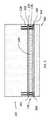
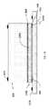
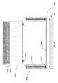
[0052] 図1〜図3は、本明細書に記載される特定の実施形態による、パッケージ中の一例の超音波デバイスの断面図を示す。図1は、超音波オンチップ100、インタポーザ106、及びプリント回路基板(PCB)160を示す。超音波オンチップ100は、シリコン貫通ビア(TSV)128及びはんだバンプ132を含む。簡潔にするために、集積回路及び超音波トランスデューサ等の超音波オンチップ100の他の構成要素は示されていない。インタポーザ106は、ヒートシンク部分140、ビア136、はんだバンプ134、及びはんだバンプ146を含む。PCB160ははんだバンプ162を含む。超音波オンチップ100(及び本明細書に記載される他の全ての超音波オンチップ)が示されるよりも多数のTSV128及びはんだバンプ132を有し得、インタポーザ106(及び本明細書に記載される他の全てのインタポーザ)が示されるよりも多数のビア136、はんだバンプ134、及びはんだバンプ146を有し得、PCB160(及び本明細書に記載される他の全てのPCB)が示されるよりも多数のはんだバンプ162を有し得ることを理解されたい。 [0052] FIGS. 1 to 3 show cross-sectional views of an example ultrasonic device in a package according to the particular embodiments described herein. FIG. 1 shows an ultrasonic on-
[0053] 超音波オンチップ100のTSV128は、超音波オンチップ100のバルクシリコン層(図1に示されず)を貫通し得るビアである。TSV128は超音波オンチップ100における1つ又は複数の集積回路及び/又は相互接続(図1に示されず)をはんだバンプ132に電気的に接続し得、はんだバンプ132は超音波オンチップ100の下面にあり、外部電気接点であり得る。TSV128は、例えば、銅、ドープポリシリコン、又はタングステンから形成し得る。超音波オンチップ100の一例は図29に見られ得る。超音波オンチップに関する追加の情報は、例えば、2015年6月30日付けで認められ(本願の譲受人に譲渡され)た「MICROFABRICATED ULTRASONIC TRANSDUCERS AND RELATED APPARATUS AND METHODS」と題する米国特許第9,067,779号に見出し得、これは全体的に参照により本明細書に援用される。 [0053] The TSV128 of the ultrasonic on-
[0054] 図1の超音波デバイスでは、超音波オンチップ100の高さ101は、製作後、パッケージ前、低減されている(例えば、研磨又はエッチングを使用して)。そのような実施形態では、超音波オンチップ100の高さは、約760μm〜800μmに等しい値又はそれらの間の値から約200μm〜300μmに等しい値又はそれらの間の値に低減し得る。超音波オンチップ100の薄化は、使用中、超音波の長波長成分を超音波オンチップ100とインタポーザ106との間の境界面において超音波オンチップ100から強制的に出すのに役立ち得、したがって、超音波オンチップ100に戻る疑似音響反射及び干渉を低減する。超音波オンチップ100とインタポーザ106との間の境界面における音響整合(例えば、裏当て材料を使用した)は、超音波オンチップ100が述べたように薄化された場合、超音波の長波長成分を強制的に出すのに必要ではないことがある。 In the ultrasonic device of FIG. 1, the
[0055] インタポーザ106のヒートシンク部分140は、窒化アルミニウム、酸化アルミニウム、ベリリウム、及び/又は低温同時焼成セラミック(LTCC)等のセラミック材料を含み得る。ヒートシンク部分140は、超音波オンチップ100から離れて熱を伝導するのに役立ち得る。例えば、セラミック材料は、超音波オンチップ100のヒートシンクとして機能できるようにするのに許容可能に高い熱伝導性を有し得る。さらに、セラミック材料は、許容可能な程度までシリコンの熱膨張係数に一致する熱膨張係数を有し得、超音波オンチップ100(シリコンを含む)及びインタポーザ106の歪みを共用可能な程度まで低減し得る。 [0055] The
[0056] はんだバンプ134はインタポーザ106の上面にあり、はんだバンプ146はインタポーザ106の下面にある。ビアははんだバンプ134をはんだバンプ146に電気的に接続する。ビア136はレーザ穴開け及びめっきにより形成し得る。 [0056] The solder bumps 134 are on the upper surface of the
[0057] PCB160は、例えば、FR4又はBTを含み得る。はんだバンプ162はPCB160の上面にあり、PCB160上又はPCB160内のトレース及び/又は回路(図1に示されず)に電気的に接続し得る。 [0057]
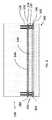
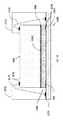
[0058] 図2では、インタポーザ106及びPCB160は一緒に結合される。インタポーザ106は、表面実装技術(SMT)プロセスを使用してPCB160に接合し得る。特に、インタポーザ106の下面におけるはんだバンプ146は、PCB160の上面におけるはんだバンプ162にはんだ接合し得る。したがって、PCB160における回路及び/又はトレースは、はんだバンプ162及び146並びにビア136を通してインタポーザ106の上面におけるはんだバンプ134に電気的に接続し得る。図2は、インタポーザ106とPCB160との間に堆積したアンダーフィル264を更に示す。アンダーフィル264は、インタポーザ106とPCB160との間のはんだボンドの機械的特性及び熱的特性の改善に役立ち得る。 [0058] In FIG. 2, the
[0059] 図3では、超音波オンチップ100及びインタポーザ106は一緒に結合される。超音波オンチップ100は、表面実装技術(SMT)プロセスを使用してインタポーザ106に接合し得る。特に、インタポーザ106の上面におけるはんだバンプ134は、超音波オンチップ100の下面におけるはんだバンプ132にはんだ接合し得る。したがって、超音波オンチップ100における集積回路及び/又は相互接続は、TSV128、はんだバンプ132及び134、ビア136、並びにはんだバンプ146及び162を通してPCB160における回路及び/又はトレースに電気的に接続し得る。図3は、超音波オンチップ100とインタポーザ106との間の境界面の全て又は実質的に全て(例えば、95%、90%、85%、80%、75%)に沿って堆積し、はんだバンプ146及び162を封入するアンダーフィル366を更に示す。アンダーフィル366は、超音波オンチップ100とインタポーザ106との間のはんだボンドの機械的特性及び熱的特性の改善に役立ち得る。 [0059] In FIG. 3, the ultrasonic on-
[0060] 幾つかの実施形態では、インタポーザ106をPCB160に結合する前、インタポーザ106を超音波オンチップ100に結合し得ることを理解されたい。 [0060] It should be understood that in some embodiments, the
[0061] 図4は、本明細書に記載される特定の実施形態による、別の例の超音波デバイスの断面図を示す。図4の超音波デバイスは、アンダーフィル366がはんだバンプ146及び162のみを封入し、超音波オンチップ100とインタポーザ106との間の境界面の残りの部分は空であるという点で図3の超音波デバイスと異なる。幾つかの実施形態では、超音波オンチップ100とインタポーザ106との間の境界面の残りの部分の実質的に全て(例えば、95%、90%、85%、80%、75%等)は空であり得る。幾つかの実施形態では、超音波オンチップ100とインタポーザ106との間の境界面の一部は空であり得る。 [0061] FIG. 4 shows a cross-sectional view of another example ultrasonic device according to the particular embodiment described herein. In the ultrasonic device of FIG. 4, the
[0062] 図5は、本明細書に記載される特定の実施形態による、別の例の超音波デバイスの断面図を示す。図5の超音波デバイスは、アンダーフィル366がはんだバンプ146及び162のみを封入し、接着剤568が超音波オンチップ100とインタポーザ106との間の境界面の残りの部分に沿って堆積するという点で図3の超音波デバイスと異なる。幾つかの実施形態では、接着剤568は、超音波オンチップ100とインタポーザ106との間の境界面の残りの部分の実質的に全て(例えば、95%、90%、85%、80%、75%等)に沿って堆積し得る。幾つかの実施形態では、接着剤568は、超音波オンチップ100とインタポーザ106との間の境界面の一部に沿って堆積し得る。接着剤568は、超音波オンチップデバイス100を出る超音波の減衰及び/又は超音波オンチップデバイス100から離れる熱伝導に役立ち得る。 [0062] FIG. 5 shows a cross-sectional view of another example ultrasonic device according to the particular embodiment described herein. In the ultrasonic device of FIG. 5, the
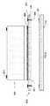
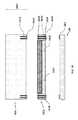
[0063] 図6は、本明細書に記載される特定の実施形態による、パッケージ中の別の例の超音波デバイスの断面図を示す。図6は、超音波オンチップ100、インタポーザ606、及びPCB160を示す。インタポーザ606は、ヒートシンク部分640、ビア636、はんだバンプ634、及びはんだバンプ646を含む。インタポーザ606は、インタポーザ606が電気的接続部分638を含むという点でインタポーザ106と異なる。したがって、インタポーザ606は、電気的接続部分638及びヒートシンク部分640を含むという点でハイブリッドインタポーザと見なし得る。電気的接続部分638はビア636、はんだバンプ634、及びはんだバンプ646を含む。電気的接続部分638は有機材料、ガラス材料、又はシリコン材料で作り得る。例えば、電気的接続部分638は、プリント回路基板の形成に標準的なプロセス及び材料(例えば、FR4又はBT)を使用して形成し得る。はんだバンプ634はインタポーザ606の上面にあり、はんだバンプ646はインタポーザ606の下面にある。ビア636は、はんだバンプ634をはんだバンプ646に電気的に接続する。ヒートシンク部分640は、電気的接続部分638に埋め込まれ得、窒化アルミニウム、酸化アルミニウム、ベリリウム、及び/又は低温同時焼成セラミック(LTCC)を含み得る。図LLLでは、アンダーフィル366ははんだバンプ132及び634を封入し、超音波オンチップ100とインタポーザ606との間の境界面の全てに沿って堆積する。しかしながら、幾つかの実施形態では、アンダーフィル366ははんだバンプ132及び634のみを封入し得、境界面の他の領域は空であり得(図4と同様に)、又は境界面のこれらの領域に沿って接着剤568が堆積し得る(図5と同様に)。 [0063] FIG. 6 shows a cross-sectional view of another example ultrasonic device in a package according to the particular embodiment described herein. FIG. 6 shows the ultrasonic on-
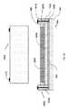
[0064] 図7は、本明細書に記載される特定の実施形態による、パッケージ中の別の例の超音波デバイスの断面図を示す。図7は、超音波オンチップ100、インタポーザ706、及びPCB160を示す。インタポーザ706は、ヒートシンク部分740、ビア736、はんだバンプ734、及びはんだバンプ746を含む。インタポーザ706は、インタポーザ706が銅パターン790、銅パターン794、及びビア792を含むという点でインタポーザ106と異なる。銅パターン790は、インタポーザ706の上面にめっきされた銅のパターンであり得る。銅パターン794は、インタポーザ706の上面にめっきされた銅のパターンであり得る。ビア736はインタポーザ706を貫通し、銅パターン790を銅パターン794に接続する。銅パターン790は超音波オンチップ100に向かって上方に突出し得、超音波オンチップ100への近さに起因して、超音波オンチップ100から離れた熱伝導の改善に役立ち得る。例えば、接合されたはんだバンプ132及び734の高さが50μmである場合、銅パターン790は高さ25μmを有し得、それにより、特定の領域における超音波オンチップ100とインタポーザ706との間のギャップを低減し得る。銅パターン790、銅パターン794、及びビア792はまた、インタポーザ706のヒートシンク部分740の強化にも役立ち得る。これは、銅パターン790が超音波オンチップ100に接触せず、超音波オンチップ100に戻る超音波反射を低減するのに有用であり得る。インタポーザ706はダイレクトプレーティング銅(DPC)インタポーザ706と見なし得る。銅パターン790、銅パターン794、及びビア792が、本明細書に記載される任意のインタポーザ又はヒートシンクに使用可能なことを理解されたい。インタポーザ706が示されるよりも多数の銅パターン790、銅パターン794、及びビア792を含み得ることも理解されたい。 [0064] FIG. 7 shows a cross-sectional view of another example ultrasonic device in a package according to the particular embodiment described herein. FIG. 7 shows the ultrasonic on-
[0065] 図1〜図7はTSVを含む超音波オンチップを示す。電気信号は、超音波オンチップからTSV、超音波オンチップに結合されたインタポーザにおけるビアを通り、PCBまで送信し得る。超音波オンチップデバイスにおけるTSVは以下の理由で有用であり得る。 [0065] FIGS. 1 to 7 show an ultrasonic on-chip containing a TSV. The electrical signal can be transmitted from the ultrasonic on-chip through the TSV, vias in the interposer coupled to the ultrasonic on-chip, to the PCB. TSVs in ultrasonic on-chip devices can be useful for the following reasons:
[0066] 1.長い電気路を必要とし得る、超音波オンチップを外部環境に電気的に接続する他の相互接続と比較して、TSVはより低い寄生インダクタンス及び抵抗を呈し得、より高い電力効率及びより低い加熱の超音波デバイスに繋がる。 [0066] 1. Compared to other interconnects that electrically connect ultrasonic on-chips to the external environment, which may require long electrical paths, TSVs can exhibit lower parasitic inductance and resistance, higher power efficiency and lower heating. Connect to the ultrasonic device of.
[0067] 2.TSVの使用により、超音波オンチップをインタポーザに結合する表面実装技術(SMT)プロセスの使用を促進し得る。インタポーザのはんだバンプの大半又は全てを超音波オンチップのはんだバンプに一度にはんだ接合することが可能であり得、1つの機械を使用して、複数の超音波オンチップを複数のインタポーザに一度にはんだ接合することが可能であり得る。換言すれば、TSVの使用は、高容量の超音波オンチップのパッケージにより適し得る高スループットパッケージプロセスを促進し得る。 [0067] 2. The use of TSVs can facilitate the use of surface mount technology (SMT) processes that couple ultrasonic on-chips to interposers. It may be possible to solder most or all of the solder bumps on the interposer to the solder bumps on the ultrasonic on-chip at once, using one machine to transfer multiple ultrasonic on-chips to multiple interposers at once. It may be possible to solder joint. In other words, the use of TSVs can facilitate a high throughput packaging process that may be more suitable for high capacity ultrasonic on-chip packaging.
[0068] 3.超音波撮像中、超音波オンチップの上面は被験者に押しつけられ得る。(撮像中、音響レンズ等の1つ又は複数の構造が超音波オンチップの上面と被験者との間に配置され得ることに留意されたい)。TSVは超音波オンチップの上面近傍に配置されず、したがって、この圧力に起因して破損を受ける程度をより低くし得る。 [0068] 3. During ultrasound imaging, the top surface of the ultrasound-on-chip can be pressed against the subject. (Note that during imaging, one or more structures, such as an acoustic lens, may be placed between the top surface of the ultrasound on-chip and the subject). The TSVs are not located near the top surface of the ultrasonic on-chip and can therefore be less likely to be damaged due to this pressure.
[0069] 4.超音波オンチップに電気的に接続する他の相互接続構造は、超音波オンチップの上面から側方に延び得る。したがって、パッケージされた超音波オンチップの上面のサイズは、この側方延長に起因して超音波オンチップ自体の上面よりも大きくなり得る。(これらのサイズを測定するために、パッケージされた超音波オンチップを鳥瞰図から下に見得る。パッケージされた超音波オンチップの上面のサイズは、超音波オンチップを下に見た場合、鳥瞰図から見えるパッケージされた超音波オンチップの総面積であり得る。超音波オンチップの上面のサイズはちょうど、超音波オンチップを下に見た場合、任意の相互接続又は他のパッケージを除いた、鳥瞰図から見える超音波オンチップの面積であり得る)。上述したように、TSVは超音波オンチップの上面近傍に配置されず、したがって、超音波オンチップの上面のサイズにはあまり寄与しない。幾つかの実施形態では、パッケージされた超音波オンチップの上面のサイズは、パッケージされていない超音波オンチップの上面のサイズと概ね同じであり得る。(例えば、パッケージされた超音波オンチップの上面のサイズは、パッケージされていない超音波オンチップの上面のサイズの100%〜101%、100%〜105%、100%〜110%、100%〜120%、100%〜125%、100%〜130%、100%〜140%、又は100%〜150%であり得る)。 [0069] 4. Other interconnect structures that electrically connect to the ultrasonic on-chip may extend laterally from the top surface of the ultrasonic on-chip. Therefore, the size of the upper surface of the packaged ultrasonic on-chip can be larger than the upper surface of the ultrasonic on-chip itself due to this lateral extension. (To measure these sizes, the packaged ultrasound on-chip can be seen below from the bird's-eye view. The size of the top surface of the packaged ultrasound on-chip is the bird's-eye view when the ultrasound on-chip is viewed below. It can be the total area of the packaged ultrasonic on-chip visible from. The size of the top surface of the ultrasonic on-chip is just the size of the top surface of the ultrasonic on-chip, excluding any interconnects or other packages, when looking down on the ultrasonic on-chip. It can be the area of the ultrasound on-chip seen from a bird's-eye view). As mentioned above, the TSVs are not located near the top surface of the ultrasonic on-chip and therefore do not contribute much to the size of the top surface of the ultrasonic on-chip. In some embodiments, the size of the top surface of the packaged ultrasound on-chip can be approximately the same as the size of the top surface of the unpackaged ultrasound-on-chip. (For example, the size of the top surface of the packaged ultrasonic on-chip is 100% to 101%, 100% to 105%, 100% to 110%, 100% to the size of the top surface of the unpackaged ultrasonic on-chip. It can be 120%, 100% to 125%, 100% to 130%, 100% to 140%, or 100% to 150%).
[0070] 相互接続を有するパッケージされた超音波オンチップの上面のサイズ増大の回避は、超音波デバイスの全体サイズの低減に役立ち得、超音波パッチ等の超音波デバイスのフォームファクタを可能にし得る。さらに、相互接続を有するパッケージされた超音波オンチップの上面のサイズ増大の回避は、例えば、撮像中、パッケージされた超音波オンチップの上面が被験者の肋骨間に嵌まるのに役立ち得る。これは特に、心臓撮像に有用であり得る。さらに、相互接続を有するパッケージされた超音波オンチップの上面のサイズ増大の回避は、パッケージされた超音波オンチップの上面に堆積する音響レンズ材料量の低減に役立ち得る。特に、音響レンズ材料の厚さの低減は、超音波デバイスにより生成される圧力波の減衰の低減に役立ち得る。 Avoiding an increase in the size of the top surface of a packaged ultrasound-on-chip with interconnects can help reduce the overall size of the ultrasound device and allow form factors for ultrasound devices such as ultrasound patches. .. In addition, avoiding an increase in the size of the top surface of the packaged ultrasound-on-chip with interconnects can help, for example, to fit the top surface of the packaged ultrasound-on-chip between the ribs of the subject during imaging. This can be particularly useful for cardiac imaging. In addition, avoiding an increase in the size of the top surface of the packaged ultrasound-on-chip with interconnects can help reduce the amount of acoustic lens material deposited on the top surface of the packaged ultrasound-on-chip. In particular, reducing the thickness of the acoustic lens material can help reduce the attenuation of the pressure waves produced by the ultrasonic device.
[0071] 本明細書に記載される任意のインタポーザ又はヒートシンクでは、インタポーザの外側部分は内側部分よりも厚くし得、溝を形成する。例えば、幾つかの実施形態では、インタポーザ606の電気的接続部分638はヒートシンク部分640よりも厚くし得る。溝は空であってもよく、又は例えば超音波オンチップとインタポーザとの境界面においてアンダーフィル若しくは接着剤を充填してもよい。 [0071] With any interposer or heat sink described herein, the outer portion of the interposer can be thicker than the inner portion, forming grooves. For example, in some embodiments, the
[0072] 図8〜図11は、本明細書に記載される特定の実施形態による、パッケージ中の別の例の超音波デバイスの断面図を示す。図8は、超音波オンチップ800、インタポーザ806、接着剤868、及びPCB160を含む。超音波オンチップ800は、超音波オンチップ800が上面にボンドパッド872を含み、TSV128を有さないという点で超音波オンチップ100と異なる。ボンドパッド872は、超音波オンチップ800内の回路及び/又は相互接続(図8では見えず)に電気的に接続し得る。インタポーザ806は、ヒートシンク部分840、ビア836、及び下面にはんだバンプ846を含む。インタポーザ806は、インタポーザ806がインタポーザ806の上部にはんだバンプを有さず、インタポーザ806の上面にボンドパッド878を更に含むという点でインタポーザ106と異なる。ビア836はボンドパッド878をはんだバンプ846に電気的に接続する。 [0072] FIGS. 8-11 show cross-sectional views of another example ultrasonic device in a package according to the particular embodiment described herein. FIG. 8 includes an ultrasonic on-
[0073] 図9では、インタポーザ806及びPCB160は一緒に結合される。インタポーザ806は、表面実装技術(SMT)プロセスを使用してPCB160に接合し得る。特に、インタポーザ806の下面におけるはんだバンプ846は、PCB160の上面におけるはんだバンプ162にはんだ接合し得る。図8は、インタポーザ806とPCB160との間に堆積したアンダーフィル264を更に示す。アンダーフィル264は、インタポーザ806とPCB160との間のはんだボンドの機械的特性及び熱的特性の改善に役立ち得る。 [0073] In FIG. 9, the
[0074] 図10では、超音波オンチップ800及びインタポーザ806は一緒に結合される。超音波オンチップ800は、接着剤868を通してインタポーザ806に接着される。幾つかの実施形態では、インタポーザ806がPCB160に結合される前、インタポーザ806を超音波オンチップ800に結合し得ることを理解されたい。 [0074] In FIG. 10, the ultrasonic on-
[0075] 図11では、超音波オンチップ800はインタポーザ806にワイヤ接合される。図11は、ワイヤボンド1174及び封入1176を含む。ワイヤボンド1174は、超音波オンチップ800上のボンドパッド872とインタポーザ806上のボンドパッド878との間に延びる。したがって、超音波オンチップ800における回路及び/又は相互接続は、ボンドパッド872、ワイヤボンド1174、ボンドパッド878、ビア836、並びにはんだバンプ846及び162を通してPCB160内の回路及び/又はトレースに電気的に接続し得る。封入1176は、ワイヤボンド1174を封入し、ワイヤボンド1174の保護及び絶縁を行うように機能し得る。示されるよりも多数のワイヤボンド1174が存在可能なことを理解されたい。 [0075] In FIG. 11, the ultrasonic on-
[0076] ワイヤボンド1174が超音波オンチップ800からインタポーザ806に延びる場合、ワイヤボンド1174は超音波オンチップ800からPCB860に延びるワイヤボンドよりも短い長さであり得る。ワイヤボンド1174が短いほど、パッケージされた超音波オンチップ800の上面を小さくし得、超音波デバイスの全体サイズの低減に役立ち得、撮像中、パッケージされた超音波オンチップ800の上面が被験者の肋骨間に嵌まるのに役立ち得、パッケージされた超音波オンチップ800の上面に堆積する音響レンズ材料量の低減に役立ち得る。 [0076] If the
[0077] 図12〜図15は、本明細書に記載される特定の実施形態による、パッケージ中の別の例の超音波デバイスの断面図を示す。図12は、超音波オンチップ800、ヒートシンク1206、接着剤868、及びPCB1260を含む。ヒートシンク1206は、ヒートシンク部分1240及び下面にはんだバンプ1246を含む。ヒートシンク1206は、ヒートシンク1206がビア836及びヒートシンク1206の上面にボンドパッド878を有さないという点でインタポーザ806と異なる。PCB1260は上面にはんだバンプ1262を含む。PCB1260は、PCB1260が上面にボンドパッド1270を含むという点でPCB160と異なる。ボンドパッド1270は、PCB1260内の回路及び/又はトレース(図12では見られず)に電気的に接続し得る。 [0077] FIGS. 12-15 show cross-sectional views of another example ultrasonic device in a package according to the particular embodiment described herein. FIG. 12 includes an ultrasonic on-
[0078] 図13では、ヒートシンク1206及びPCB1260は一緒に結合される。ヒートシンク1206は、表面実装技術(SMT)プロセスを使用してPCB1260に接合し得る。特に、ヒートシンク1206の下面におけるはんだバンプ1246は、PCB1260の上面におけるはんだバンプ1262にはんだ接合し得る。図13は、ヒートシンク1206とPCB1260との間に堆積したアンダーフィル264を更に示す。アンダーフィル264は、ヒートシンク1206とPCB1260との間のはんだボンドの機械的特性及び熱的特性の改善に役立ち得る。 [0078] In FIG. 13, the
[0079] 図14では、本明細書に記載される特定の実施形態によれば、超音波オンチップ800及びヒートシンク1206は一緒に結合される。超音波オンチップ800は、接着剤868を通してヒートシンク1206に接着される。幾つかの実施形態では、インタポーザ806がPCB1260に結合される前、ヒートシンク1206を超音波オンチップ800に結合し得ることを理解されたい。 [0079] In FIG. 14, according to the particular embodiments described herein, the ultrasonic on-
[0080] 図15では、超音波オンチップ800はPCB1260にワイヤ接合される。図15はワイヤボンド1574及び封入1576を含む。ワイヤボンド1574は、超音波オンチップ800におけるボンドパッド872とPCB1260におけるボンドパッド1270との間に延びる。したがって、超音波オンチップ800における回路及び/又は相互接続は、ボンドパッド872、ワイヤボンド1574、及びボンドパッド1270を通してPCB1260内の回路及び/又はトレースに電気的に接続し得る。封入1576はワイヤボンド1574を封入し、ワイヤボンド1574の保護及び絶縁を行うように機能し得る。示されるよりも多数のワイヤボンド1574があり得ることを理解されたい。 [0080] In FIG. 15, the ultrasonic on-
[0081] 図12〜図15において見て取ることができるように、ワイヤボンド1574が超音波オンチップ800からPCB1260に延びる場合、ヒートシンク1266は、本明細書に記載される他のインタポーザのようにビアを含まないことがある。 [0081] As can be seen in FIGS. 12-15, when the
[0082] 図16〜図18は、本明細書に記載される特定の実施形態による、パッケージ中の超音波デバイスの別の例の断面図を示す。図16は超音波オンチップ1600、インタポーザ1606、及びプリント回路基板(PCB)160を示す。 [0082] FIGS. 16-18 show cross-sectional views of another example of an ultrasonic device in a package according to the particular embodiment described herein. FIG. 16 shows an ultrasonic on-
[0083] 超音波オンチップ1600は、シリコン貫通ビア(TSV)1628及びはんだバンプ1632を含む。超音波オンチップ1600は、超音波オンチップ1600の高さ1601が、製作後、パッケージ前、低減されないという点で超音波オンチップ100と異なる。したがって、超音波オンチップ1600の高さは約760μm〜800μmに等しい値又はそれらの間の値であり得る。 [0083] The ultrasonic on-
[0084] インタポーザ1606は、ヒートシンク部分1640、電気的接続部分1638、ビア1636、はんだバンプ1634、及びはんだバンプ1646を含む。インタポーザ1606は、電気的接続部分1638がヒートシンク部分1640よりも厚く、裏当て材料1604のための溝を形成するという点でインタポーザ606と異なる。 The
[0085] 裏当て材料1604はインタポーザ1606の上面に結合される。しかしながら、幾つかの実施形態では、裏当て材料1604は超音波オンチップ1600の下面に結合し得る。幾つかの実施形態では、裏当て材料1604の厚さは約400μm〜600μmに等しい値又はそれらの間の値であり得る。幾つかの実施形態では、裏当て材料1604はタングステン含有エポキシを含み得る。幾つかの実施形態では、エポキシは2段階エポキシであり得、第1の硬化段階は、裏当て材料1604をインタポーザ1606に結合するために実行し得、第2の硬化段階は、超音波オンチップ1600を裏当て材料1604に結合するために実行し得る。幾つかの実施形態では、裏当て材料1604は、インタポーザ1606の上面が、重力により裏当て材料1604がインタポーザ1606上に定まるように上方に面する場合、インタポーザ1606にスクリーンプリントし得る。幾つかの実施形態では、裏当て材料1604は超音波オンチップ1600の下面に結合し得、裏当て材料1604は、インタポーザ1606の下面が、重力により裏当て材料1604が超音波オンチップ1600上に定まるように上面に面する場合、超音波オンチップ1600にスクリーンプリントし得る。 [0085] The
[0086] 上述したように、超音波オンチップ1600の高さは、製作後、低減されない(例えば、研磨又はエッチングを使用して)。したがって、超音波オンチップ1600の高さは約760μm〜800μmに等しい値又はそれらの間の値であり得る。超音波オンチップ1600とインタポーザ1606との間の境界面における裏当て材料1604は、音響整合機能を提供し得、超音波の長波長成分を裏当て材料1604を通して超音波オンチップから強制的に出し得、裏当て材料1604において減衰させ得、したがって、超音波オンチップ1600に戻る疑似音響反射及び干渉を低減する。超音波オンチップ1600の高さを維持する(薄化させるのではなく)ことは、パッケージ中、超音波デバイスの取り扱いに有用であり得る。 [0086] As mentioned above, the height of the ultrasonic on-
[0087] 幾つかの実施形態では、裏当て材料1604は超音波オンチップ1600とインタポーザ1606との間に配置されるため、インタポーザ1606の高さ、ひいてはインタポーザ1606におけるビア1636の高さは、裏当て材料1604の厚さに依存し得る。ビア1636が長いほど、超音波オンチップ1600からインタポーザ1606及びPCB160への高インダクタンス及び/又は高抵抗の電気接続の一因になり得る。高インダクタンスの回避は特に、超音波信号の生成に必要であり得る電流の大きなスパイクに起因して、超音波オンチップ1600において有用であり得る。幾つかの実施形態では、裏当て材料1604の厚さの選択は、音響減衰、インタポーザ1606のヒートシンク部分1640への熱伝導効率、及びインダクタンス間のトレードオフを含み得る。例えば、幾つかの実施形態では、音響減衰は裏当て材料1604の厚さ増大に伴って増大し得、インタポーザ1606のヒートシンク部分1640への熱伝導効率は、裏当て材料1604の厚さ増大に伴って低減し得、インダクタンス及び/又は抵抗は、裏当て材料1604の厚さ増大に伴って増大し得る。 [0087] In some embodiments, the
[0088] 図17では、インタポーザ1606及びPCB160は一緒に結合される。インタポーザ1606は、表面実装技術(SMT)プロセスを使用してPCB160に接合し得る。特に、インタポーザ1606の下面におけるはんだバンプ1646は、PCB160の上面におけるはんだバンプ162にはんだ接合し得る。したがって、PCB160における回路及び/又はトレースは、はんだバンプ162及び1646並びにビア1636を通してインタポーザ1606の上面におけるはんだバンプ1634に電気的に接続し得る。図17は、インタポーザ1606とPCB160との間に堆積したアンダーフィル264を更に示す。アンダーフィル264は、インタポーザ1606とPCB160との間のはんだボンドの機械的特性及び熱的特性の改善に役立ち得る。 [0088] In FIG. 17, the
[0089] 図18では、超音波オンチップ1600及びインタポーザ1606は一緒に結合される。超音波オンチップ1600は、表面実装技術(SMT)プロセスを使用してインタポーザ1806に接合し得る。特に、インタポーザ1606の上面におけるはんだバンプ1634は、超音波オンチップ1600の下面におけるはんだバンプ1632にはんだ接合し得る。したがって、超音波オンチップ1600における集積回路及び/又は相互接続は、TSV1628、はんだバンプ1632及び1634、ビア1636、並びにはんだバンプ1646及び162を通してPCB160における回路及び/又はトレースに電気的に接続し得る。上述したように、裏当て材料1604の第2の硬化段階を実行して、超音波オンチップ1600をインタポーザ1606における裏当て材料1604に結合し得る。図18は、はんだバンプ1634と1636との間の境界面において超音波オンチップ1600とインタポーザ1606との間に堆積したアンダーフィル366を更に示す。アンダーフィル366は、超音波オンチップ1600とインタポーザ1606との間のはんだボンドの機械的特性及び熱的特性の改善に役立ち得る。裏当て材料1604は、境界面の他の部分において超音波オンチップ1600とインタポーザ1606との間に堆積する。見て取ることができるように、超音波オンチップ1600は、超音波オンチップ1600及びインタポーザ1606が一緒に結合される場合、インタポーザ1606のヒートシンク部分1640上に置かれる。特に、裏当て材料1604の下面の実質的に全て(例えば、100%、99%、95%、90%、又は75%)は、超音波オンチップ1600及びインタポーザ1606が一緒に結合される場合、熱伝導性接着剤を通してインタポーザ1606のヒートシンク部分1640に結合し得る。インタポーザ1606は、超音波オンチップ1600から裏当て材料1604、ヒートシンク部分1640を通して、パッケージされた超音波オンチップ1600の底及び横から出る熱伝導の確立に寄与するように構成し得る。幾つかの実施形態では、インタポーザ1606がPCB160に結合される前、インタポーザ1606を超音波オンチップ1600に結合し得ることを理解されたい。 [0089] In FIG. 18, the ultrasonic on-
[0090] 図16〜図18は、TSVを含む超音波オンチップデバイスを示す。これらのTSVは、図1〜図7を参照して上述した理由と同じ理由で有用であり得る。 [0090] FIGS. 16-18 show ultrasonic on-chip devices including TSVs. These TSVs may be useful for the same reasons as described above with reference to FIGS. 1-7.
[0091] 図19〜図22は、本明細書に記載される特定の実施形態による、パッケージ中の別の例の超音波デバイスの断面図を示す。図19は超音波オンチップ1900、インタポーザ1906、裏当て材料1604、及びPCB160を示す。超音波オンチップ1900は、超音波オンチップ1900が超音波オンチップ1900の上面にボンドパッド1972を含み、超音波オンチップ1900にビアを有さず、超音波オンチップ1900の下面にはんだバンプを有さないという点で超音波オンチップ1600と異なる。インタポーザ1906は、電気的接続部分1938、ヒートシンク部分1940、ビア1936、及びインタポーザ1906の下面におけるはんだバンプ1946を含む。インタポーザ1906は、インタポーザ1906が電気的接続部分1938から内側に延びるレッジ1980を更に含み、インタポーザ1906の上面にボンドパッド1978を含み、インタポーザ1906の上面にはんだバンプを有さないという点でインタポーザ1606と異なる。ビア1936は、ボンドパッド1978をはんだバンプ1946に電気的に接続する。 [0091] FIGS. 19-22 show cross-sectional views of another example ultrasonic device in a package according to the particular embodiment described herein. FIG. 19 shows an ultrasonic on-
[0092] 図20では、インタポーザ1906及びPCB160は一緒に結合される。インタポーザ1906は、表面実装技術(SMT)プロセスを使用してPCB160に接合し得る。特に、インタポーザ1906の下面におけるはんだバンプ1946は、PCB160の上面におけるはんだバンプ162にはんだ接合し得る。したがって、PCB160における回路及び/又はトレースは、はんだバンプ162及び1946並びにビア1936を通してインタポーザ1906の上面におけるボンドパッド1978に電気的に接続し得る。図20は、インタポーザ1906とPCB160との間に堆積したアンダーフィル264を更に示す。アンダーフィル264は、インタポーザ1906とPCB160との間のはんだボンドの機械的特性及び熱的特性の改善に役立ち得る。 [0092] In FIG. 20, the
[0093] 図21では、超音波オンチップ1900及びインタポーザ1906は一緒に結合される。超音波オンチップ1900はレッジ1980上に静止する。幾つかの実施形態では、超音波オンチップ1900は、レッジ1980上の接着剤に結合し得る。これは、超音波オンチップ1900とインタポーザ1906との間にはんだ接合がない場合、超音波デバイスの構造的整合性を保証し得る。超音波オンチップ1900はまた、裏当て材料1604に結合することもできる。幾つかの実施形態では、インタポーザ1906がPCB160に結合される前、インタポーザ1906を超音波オンチップ1900に結合し得ることを理解されたい。 [0093] In FIG. 21, the ultrasonic on-
[0094] 図22では、超音波オンチップ1900はインタポーザ1906にワイヤ接合される。図22はワイヤボンド2274及び封入2276を含む。ワイヤボンド2274は、超音波オンチップ1900におけるボンドパッド1972とインタポーザ1906におけるボンドパッド1978との間に延びる。したがって、超音波オンチップ1900における回路及び/又は相互接続は、ボンドパッド1972、ワイヤボンド2274、ボンドパッド1978、ビア1936、並びにはんだバンプ1946及び162を通してPCB160内の回路及び/又はトレースに電気的に接続し得る。封入2276はワイヤボンド2274を封入し、ワイヤボンド2274の保護及び絶縁を行うように機能し得る。示されるよりも多数のワイヤボンド2274が存在可能なことを理解されたい。 [0094] In FIG. 22, the ultrasonic on-
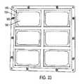
[0095] 図23は、本明細書に記載される特定の実施形態によるインタポーザ1906の一例の鳥瞰図を示す。特に、図23は6つのハイブリッドインタポーザ1906を示し、各ハイブリッドインタポーザは、電気的接続部分1938、ヒートシンク部分1940(例えば、窒化アルミニウム、酸化アルミニウム、ベリリウム、及び/又は低温同時焼成セラミック(LTCC))、及び電気的接続部分1938から内側に延びるレッジ1980を含む。超音波オンチップ1900をインタポーザ1906に結合するために、超音波オンチップ1900は、図23において見えるインタポーザ1906の上面に下降し得る。 [0095] FIG. 23 shows a bird's-eye view of an example of
[0096] 図24〜図28は、本明細書に記載される特定の実施形態による別の例の超音波デバイスの断面図を示す。図24は、超音波オンチップ1900、裏当て材料1604、ヒートシンク2482、インタポーザ2406、ライナー2484、及びPCB160を示す。超音波オンチップ1900は、図19の向きから垂直方向において反転されて示されている。裏当て材料1604は超音波オンチップ1900に結合され(例えば、図24において見えない接着剤を通して)、ヒートシンク2482は裏当て材料1604に結合される(例えば、図24において見えない接着剤を通して)。ヒートシンク2482は、窒化アルミニウム、酸化アルミニウム、ベリリウム、及び/又は低温同時焼成セラミック(LTCC)等のセラミック材料を含み得る。インタポーザ2406は、ビア2436及びボンドパッド2478を含む。ビア2436はボンドパッド2478に電気的に接続される。インタポーザ2406は有機材料、ガラス材料、又はシリコン材料で作られ得る。ライナー2484はボンドパッド2478を保護し得る。ライナー2484は、残留物なしの取り外し可能なライナーであり得、例えば、ポリイミドテープ、フィルム、又はシートを含み得る。幾つかの実施形態では、ライナー2484は静電放電散逸性であり得る。インタポーザ2406は、図24では2つの接続されていない部分として現れるが、図24では見えないインタポーザ2406の他の部分はこれらの2つの部分を一緒に接続し得る。幾つかの実施形態では、インタポーザ2406は額縁に類似し得る。 [0096] FIGS. 24 to 28 show cross-sectional views of another example ultrasonic device according to the particular embodiment described herein. FIG. 24 shows an ultrasonic on-
[0097] 図25では、超音波オンチップ1900はインタポーザ2406に結合される。超音波オンチップ1900は、ボンドパッド1972を含む超音波オンチップ1900の面がライナー2484に面するようにインタポーザ2406に挿入される。超音波オンチップ1900は、接着剤2488を用いてインタポーザ2406に接着される。ライナー2486は、ライナー2484によりまだ覆われていない超音波超音波オンチップ1900及びインタポーザ2406の面を覆って配置される。 [0097] In FIG. 25, the ultrasonic on-
[0098] 図26では、超音波オンチップ1900はインタポーザ2406にワイヤ接合される。PCB160を除く図26における全ての要素は、図25の向きから垂直において反転されて示されている。図26はワイヤボンド2674及び封入2676を含む。ライナー2484は除去されている。ワイヤボンド2674は、超音波オンチップ1900におけるボンドパッド1972とインタポーザ2406におけるボンドパッド2478との間に延びる。封入2676はワイヤボンド2674を封入し、ワイヤボンド2674の保護及び絶縁を行うように機能し得る。示されるよりも多数のワイヤボンド2674が存在し得ることを理解されたい。 [0098] In FIG. 26, the ultrasonic on-
[0099] 図27では、ライナー186は除去されている。はんだバンプ2746は、はんだバンプ2746がビア2436に電気的に接続されるようにインタポーザ2406に配置されている。したがって、ビア2436はボンドパッド2478をはんだバンプ2746に電気的に接続する。 [0099] In FIG. 27, the liner 186 has been removed. The solder bumps 2746 are arranged on the
[00100] 図28では、インタポーザ2406はPCB160に結合される。インタポーザ2406は、表面実装技術(SMT)プロセスを使用してPCB160に接合し得る。特に、インタポーザ2406の下面におけるはんだバンプ2746は、PCB160の上面におけるはんだバンプ162にはんだ接合し得る。したがって、PCB160における回路及び/又はトレースは、はんだバンプ162及び146、ビア2436、ボンドパッド2478、ワイヤボンド2674、並びにボンドパッド1972を通して超音波オンチップ1900における回路及び/又は相互接続に電気的に接続し得る。図28は、インタポーザ2406とPCB160との間に堆積したアンダーフィル264を更に示す。アンダーフィル264は、インタポーザ2406とPCB160との間のはんだボンドの機械的特性及び熱的特性の改善に役立ち得る。 [00100] In FIG. 28, the
[00101] 図29は、本明細書に記載される特定の実施形態による一例の超音波オンチップ2900を示す。超音波オンチップ2900は、相補型金属酸化膜半導体(CMOS)基板等の集積回路基板2903に接合された超音波トランスデューサ基板2902を含む。超音波トランスデューサ基板2902は、複数のキャビティ2914、第1のシリコンデバイス層2918、第2のシリコンデバイス層2912、酸化シリコン層2920、パッシベーション層2908、酸化シリコン部分2916、及びメタライゼーション2910を含む。キャビティ2914は、第1のシリコンデバイス層2918と第2のシリコンデバイス層2912との間に形成される。酸化シリコン層2920(例えば、シリコンの熱酸化により形成される酸化シリコン等の熱酸化シリコン)は、キャビティ2914が形成された状態で第1のシリコンデバイス層2918と第2のシリコンデバイス層2912との間に形成される。キャビティ2914は、酸化シリコンを含む2つの基板を一緒に接合することにより形成し得る。酸化シリコン部分2916は、接合前、他方の基板にあった酸化シリコン層2920に接合された一方の基板上の酸化シリコン層を表し得る。この非限定的な例では、第1のシリコンデバイス層2918は下部電極として構成し得、第2のシリコンデバイス層2912はメンブレンとして構成し得る。したがって、第1のシリコンデバイス層2918、第2のシリコンデバイス層2912、及びキャビティ2914の組合せは、超音波トランスデューサ(例えば、容量性微細加工超音波トランスデューサ(CMUT))を形成し得、そのうちの6つがこの非限定的な断面図に示されている。下部電極又はメンブレンとしての動作を促進するために、第1のシリコンデバイス層2918及び第2のシリコンデバイス層2912の一方又は両方は、導体として機能するようにドープし得、幾つかの場合、高ドープ(例えば、1015ドーパント/cm3を超えるドープ濃度又はそれを超えるドープ濃度を有する)し得る。パッシベーション層2908は、第1のシリコンデバイス層2918をパッシベートする。メタライゼーション2910は、外部電気接点を超音波トランスデューサに提供する。超音波オンチップの上面2944は、撮像のために超音波エネルギーを超音波トランスデューサから送る面を表す。したがって、上面2944は、超音波オンチップ2900が一部である超音波デバイスのセンサ面を表す。[00101] FIG. 29 shows an example ultrasonic on-
[00102] 集積回路基板2903は、メタライゼーション2942、絶縁層2922、バルクシリコン層2930、シリコン貫通ビア(TSV)2928、及びはんだバンプ2932を含む。(本明細書に記載されるはんだバンプはめっきされ、次に、アニーリングされて、ハーフドーム基板を形成し得る)。メタライゼーション2942は、アルミニウム、銅、又は任意の他の適したメタライゼーション材料で形成し得、集積回路基板2903に形成される集積回路の少なくとも一部を表し得る。例えば、メタライゼーション2942は、ルーティング層として機能し得、1つ若しくは複数の電極を形成するようにパターニングし得、又は他の機能に利用し得る。実際には、集積回路基板2903は2つ以上のメタライゼーション層を含み得るが、簡潔にするために、1つのみのメタライゼーション2942が示されている。 [00102] The integrated
[00103] TSV2928は、バルクシリコン層2930を貫通するビアである。TSV2928は、集積回路基板2903に含まれる1つ又は複数の集積回路と、超音波オンチップ2900の下面2948(すなわち、上面2944の逆の表面)にあり、外部電気接点であり得るはんだバンプ2932との間で電気信号を伝送し得る。TSV2928は、例えば、銅、ドープポリシリコン、又はタングステンから形成し得る。(TSV2928と集積回路基板2903における集積回路との間の電気接続は図29に示されていない)。幾つかの実施形態では、TSV2928及びはんだバンプ2932はなくてもよい。 [00103] TSV2928 is a via that penetrates the
[00104] 超音波オンチップ2900は、接合構造2926及び接合構造2926を形成する準備として形成されるパッシベーション層2924を更に含む。接合構造2926は、超音波トランスデューサ基板2902を集積回路基板2903に電気的に接続する。したがって、電気信号は、集積回路基板2903から接合構造2926を通り超音波トランスデューサ基板2902まで送信し得、この逆も同様である。 [00104] The ultrasonic on-
[00105] 本明細書に記載される特定の実施形態により、超音波オンチップ2900の高さ2901が低減される場合、これは、バルクシリコン層2930の高さを低減することにより達成し得ることを理解されたい。 [00105] If the
[00106] CMOSウェーハを有するCMUTの製作及び集積に関する追加の情報は、例えば、2015年6月30日付けで認められ(本願の譲受人に譲渡され)た「MICROFABRICATED ULTRASONIC TRANSDUCERS AND RELATED APPARATUS AND METHODS」と題する米国特許第9,067,779号に見出し得る。しかしながら、図29に示される実施形態が、超音波オンチップ2900に可能な構成の単なる1つを表すことを理解されたい。限定ではなく、トランスデューサ及び集積回路が同じ基板に形成されるサイドバイサイド配置並びに圧電性微細加工超音波トランスデューサ(PMUT)から形成されるアレイ、又は他の適したタイプの超音波トランスデューサを含め、他の構成も可能である。更に他の実施形態では、超音波オンチップデバイス2900は、それ自体で超音波トランスデューサアレイを含み得(すなわち、超音波トランスデューサチップ)、集積回路は異なる基板に配置され、又は一緒に回路基板に配置される。 [00106] Additional information regarding the fabrication and integration of CMUTs with CMOS wafers is, for example, "MICRO FABRICATED ULTRASONIC TRANSDUCERS AND RELATED APPARATUS AND METHODS" approved (assigned to the assignee of the present application) on June 30, 2015. Can be found in US Pat. No. 9,067,779, entitled. However, it should be understood that the embodiment shown in FIG. 29 represents just one of the possible configurations for the ultrasonic on-
[00107] 図30は、本明細書に記載される特定の実施形態による超音波オンチップをパッケージする一例のプロセス3000を示す。プロセス3000の更なる説明は、図1〜図7及び図16〜図18を参照して見出し得る。 [00107] FIG. 30 shows an
[00108] 動作3002において、超音波オンチップは厚さ低減される。特に、超音波オンチップ100の高さが、製作後、パッケージに先立って低減される(例えば、研磨又はエッチングを使用して)。そのような実施形態では、超音波オンチップの高さは、約760μm〜800μmに等しい値又はそれらの間の値から約200μm〜300μmに等しい値又はそれらの間の値に低減し得る。超音波オンチップの薄化は、使用中、超音波の長波長成分を超音波オンチップから強制的に出すのに役立ち得、したがって、超音波オンチップに戻る疑似音響反射及び干渉を低減する。幾つかの実施形態では、動作3002はなくてもよく、超音波オンチップの厚さは低減されない。幾つかの実施形態では、超音波オンチップは、裏当て材料に結合されていてもよい。裏当て材料1604の厚さは約400μm〜600μmに等しい値又はそれらの間の値であり得、タングステンを含むエポキシを含み得、超音波オンチップ又はインタポーザにスクリーンプリントし得る(後述するように)。プロセス3000は動作3002から動作3004に進む。 [00108] In
[00109] 動作3004において、インタポーザは、インタポーザ内のビアがPCBに電気的に接続されるようにプリント回路基板に結合される。例えば、インタポーザ内のビアに電気的に接続されたインタポーザ上のはんだバンプをPCB上のはんだバンプに接合し得る。幾つかの実施形態では、インタポーザは、窒化アルミニウム、酸化アルミニウム、ベリリウム、及び/又は低温同時焼成セラミック(LTCC)等のセラミック材料を含むヒートシンク部分を含み、ビアはヒートシンク部分を貫通する。幾つかの実施形態では、インタポーザはヒートシンク部分及び電気的接続部分の両方を含み、電気的接続部分は有機材料、ガラス材料、又はシリコン材料を含み、ビアは電気的接続部分を貫通する。裏当て材料を含む実施形態では、裏当て材料は超音波オンチップとインタポーザとの間に配置し得る。プロセス3000は動作3004から動作3006に進む。 [00109] In
[00110] 動作3006において、超音波オンチップは、超音波オンチップ内のTSVがインタポーザ内のビアに電気的に接続されるようにインタポーザに結合される。例えば、超音波オンチップ内のTSVに電気的に接続された超音波オンチップ上のはんだバンプは、インタポーザ内のビアに電気的に接続されたインタポーザ上のはんだバンプに接合し得る。 [00110] In
[00111] 超音波オンチップデバイスにおけるTSVは以下の理由で有用であり得る。 [00111] TSVs in ultrasonic on-chip devices can be useful for the following reasons:
[00112] 1.長い電気路を必要とし得る、超音波オンチップを外部環境に電気的に接続する他の相互接続と比較して、TSVはより低い寄生インダクタンス及び抵抗を呈し得、より高い電力効率及びより低い加熱の超音波デバイスに繋がる。 [00112] 1. Compared to other interconnects that electrically connect ultrasonic on-chips to the external environment, which may require long electrical paths, TSVs can exhibit lower parasitic inductance and resistance, higher power efficiency and lower heating. Connect to the ultrasonic device of.
[00113] 2.TSVの使用により、超音波オンチップをインタポーザに結合する表面実装技術(SMT)プロセスの使用を促進し得る。インタポーザのはんだバンプの大半又は全てを超音波オンチップのはんだバンプに一度にはんだ接合することが可能であり得、1つの機械を使用して、複数の超音波オンチップを複数のインタポーザに一度にはんだ接合することが可能であり得る。換言すれば、TSVの使用は、高容量の超音波オンチップのパッケージにより適し得る高スループットパッケージプロセスを促進し得る。 [00113] 2. The use of TSVs can facilitate the use of surface mount technology (SMT) processes that couple ultrasonic on-chips to interposers. It may be possible to solder most or all of the solder bumps on the interposer to the solder bumps on the ultrasonic on-chip at once, using one machine to transfer multiple ultrasonic on-chips to multiple interposers at once. It may be possible to solder joint. In other words, the use of TSVs can facilitate a high throughput packaging process that may be more suitable for high capacity ultrasonic on-chip packaging.
[00114] 3.超音波撮像中、超音波オンチップの上面は被験者に押しつけられ得る。(撮像中、音響レンズ等の1つ又は複数の構造が超音波オンチップの上面と被験者との間に配置され得ることに留意されたい)。TSVは超音波オンチップの上面近傍に配置されず、したがって、この圧力に起因して破損を受ける程度をより低くし得る。 [00114] 3. During ultrasound imaging, the top surface of the ultrasound-on-chip can be pressed against the subject. (Note that during imaging, one or more structures, such as an acoustic lens, may be placed between the top surface of the ultrasound on-chip and the subject). The TSVs are not located near the top surface of the ultrasonic on-chip and can therefore be less likely to be damaged due to this pressure.
[00115] 4.超音波オンチップに電気的に接続する他の相互接続構造は、超音波オンチップの上面から側方に延び得る。したがって、パッケージされた超音波オンチップの上面のサイズは、この側方延長に起因して超音波オンチップ自体の上面よりも大きくなり得る。上述したように、TSVは超音波オンチップの上面近傍に配置されず、したがって、超音波オンチップの上面のサイズにはあまり寄与しない。相互接続を有するパッケージされた超音波オンチップの上面のサイズ増大の回避は、超音波デバイスの全体サイズの低減に役立ち得、超音波パッチ等の超音波デバイスのフォームファクタを可能にし得る。さらに、相互接続を有するパッケージされた超音波オンチップの上面のサイズ増大の回避は、例えば、撮像中、パッケージされた超音波オンチップの上面が被験者の肋骨間に嵌まるのに役立ち得る。これは特に、心臓撮像に有用であり得る。さらに、相互接続を有するパッケージされた超音波オンチップの上面のサイズ増大の回避は、パッケージされた超音波オンチップの上面に堆積する音響レンズ材料量の低減に役立ち得る。特に、音響レンズ材料の厚さの低減は、超音波デバイスにより生成される圧力波の減衰の低減に役立ち得る。 [00115] 4. Other interconnect structures that electrically connect to the ultrasonic on-chip may extend laterally from the top surface of the ultrasonic on-chip. Therefore, the size of the upper surface of the packaged ultrasonic on-chip can be larger than the upper surface of the ultrasonic on-chip itself due to this lateral extension. As mentioned above, the TSVs are not located near the top surface of the ultrasonic on-chip and therefore do not contribute much to the size of the top surface of the ultrasonic on-chip. Avoiding an increase in the size of the top surface of a packaged ultrasound on-chip with interconnects can help reduce the overall size of the ultrasound device and allow form factors for ultrasound devices such as ultrasound patches. In addition, avoiding an increase in the size of the top surface of the packaged ultrasound on-chip with interconnects can help, for example, to fit the top surface of the packaged ultrasound-on-chip between the ribs of the subject during imaging. This can be particularly useful for cardiac imaging. In addition, avoiding an increase in the size of the top surface of the packaged ultrasound-on-chip with interconnects can help reduce the amount of acoustic lens material deposited on the top surface of the packaged ultrasound-on-chip. In particular, reducing the thickness of the acoustic lens material can help reduce the attenuation of the pressure waves produced by the ultrasonic device.
[00116] 幾つかの実施形態では、動作3006は動作3004に先だって実行し得る。換言すれば、インタポーザは、PCBに結合される前、超音波オンチップに結合し得る。幾つかの実施形態では、動作3004はなくてもよく、そのような実施形態では、インタポーザは別のタイプのデバイスに結合し得、又は別のデバイスに結合されない。 [00116] In some embodiments,
[00117] 図31は、本明細書に記載される特定の実施形態による超音波オンチップをパッケージする別の例のプロセス3100を示す。プロセス3100の更なる説明は、図8〜図11、図19〜図22、及び図24〜図28を参照して見出し得る。 [00117] FIG. 31 shows another
[00118] 動作3102において、超音波オンチップは厚さ低減される。動作3102の更なる説明は動作3002を参照して見出し得る。上述したように、幾つかの実施形態では、動作3102はなくてもよい。プロセス3100は動作3102から動作3104に進む。 [00118] In
[00119] 動作3104において、インタポーザは、インタポーザ内のビアがPCBに電気的に接続されるようにプリント回路基板に結合される。動作3104の更なる説明は動作3004を参照して見出し得る。プロセス3100は動作3104から動作3106に進む。 [00119] In
[00120] 動作3106において、超音波オンチップはインタポーザに結合される。例えば、超音波オンチップは接着剤を通してインタポーザに結合し得る。プロセス3100は動作3106から動作3108に進む。 [00120] In
[00121] 幾つかの実施形態では、動作3106は動作3104に先立って実行し得る。換言すれば、インタポーザは、PCBに結合される前、超音波オンチップに結合し得る。幾つかの実施形態では、動作3104はなくてもよく、そのような実施形態では、インタポーザは別のタイプのデバイスに結合し得、又は別のデバイスに結合されない。 [00121] In some embodiments, the
[00122] 動作3108において、超音波オンチップはインタポーザにワイヤ接合される。例えば、ワイヤボンドは、超音波オンチップ上のボンドパッドからインタポーザ上のボンドパッドに延び得る。ワイヤボンドが超音波オンチップからインタポーザに延びる場合、ワイヤボンドは、超音波オンチップからPCBまで延びるワイヤボンドよりも短い長さであり得る。ワイヤボンドが短いほど、パッケージされた超音波オンチップの上面は小さくなり得、超音波デバイスの全体サイズの低減に役立ち得、撮像中、被験者の肋骨間にパッケージされた超音波オンチップの上面を嵌めるのに役立ち得、パッケージされた超音波オンチップの上面に堆積する音響レンズ材料量の低減に役立ち得る。 [00122] In
[00123] 図32は、本明細書に記載される特定の実施形態による超音波オンチップをパッケージする別の例のプロセス3100を示す。プロセス3200の更なる説明は図12〜図15を参照して見出し得る。 [00123] FIG. 32 shows another
[00124] 動作3202において、超音波オンチップは厚さ低減される。動作3202の更なる説明は動作3002を参照して見出し得る。プロセス3200は動作3202から動作3204に進む。 [00124] In
[00125] 動作3204において、ヒートシンクはプリント回路基板(PCB)に結合される。例えば、ヒートシンクは、表面実装技術によりプリント回路基板に結合し得る。プロセス3200は動作3204から動作3206に進む。 [00125] In
[00126] 動作3206において、超音波オンチップはヒートシンクに結合される。例えば、超音波オンチップは、接着剤又は表面実装技術によりヒートシンクに結合し得る。ヒートシンクは、窒化アルミニウム、酸化アルミニウム、ベリリウム、及び/又は低温同時焼成セラミック(LTCC)等のセラミック材料を含み得る。プロセス3200は動作3206から動作3208に進む。 [00126] In
[00127] 幾つかの実施形態では、動作3206は動作3204に先立って実行し得る。換言すれば、ヒートシンクは、PCBに結合される前、超音波オンチップに結合し得る。幾つかの実施形態では、動作3204はなくてもよく、ヒートシンクは別のタイプのデバイスに結合し得、又は別のデバイスに結合されない。 [00127] In some embodiments, the
[00128] 動作3208において、超音波オンチップはPCBにワイヤ接続される。例えば、ワイヤボンドは、超音波オンチップ上のボンドパッドからPCB上のボンドパッドに延び得る。ワイヤボンドが超音波オンチップからPCBに延びる場合、ヒートシンクは、プロセス3000及び3100を参照して説明したインタポーザ等の他のインタポーザのようにはビアを含まなくてよい。 [00128] In
[00129] 上記説明は、超音波オンチップに使用し得るパッケージ方式を説明したが、パッケージ方式が他のタイプのダイにも同様に使用可能なことを理解されたい。例えば、本明細書に記載される任意のインタポーザは、他のタイプのダイと組み合わせて使用し得る。 [00129] Although the above description has described a packaging scheme that can be used for ultrasonic on-chip, it should be understood that the packaging scheme can be used for other types of dies as well. For example, any interposer described herein can be used in combination with other types of dies.
[00130] 本開示の種々の態様は、単独で、組み合わせて、又は上述した実施形態において特に考察されていない多種多様な構成で使用し得、したがって、用途は、上記説明に記載され、又は図面に示される構成要素の詳細及び構成に限定されない。例えば、一実施形態に記載された態様は、他の実施形態に記載された態様と任意の様式で組合せ得る。 [00130] The various aspects of the present disclosure may be used alone, in combination, or in a wide variety of configurations not specifically discussed in the embodiments described above, and thus the applications are described in the above description or in the drawings. It is not limited to the details and composition of the components shown in. For example, the embodiments described in one embodiment may be combined with the embodiments described in other embodiments in any manner.
[00131] 不定冠詞「a」及び「an」は、本明細書及び特許請求の範囲で使用される場合、逆のことが明記される場合を除き、「少なくとも1つ」を意味するものと理解されたい。 [00131] The indefinite articles "a" and "an" are understood to mean "at least one" when used herein and in the claims, unless otherwise specified. I want to be.
[00132] 句「及び/又は」は、本明細書及び特許請求の範囲で使用される場合、そうして等位接続される要素の「何れか又は両方」、すなわち、結合的に存在することもあれば、分離して存在することもある要素を意味するものと理解されたい。「及び/又は」を用いて列記される複数の要素は、同一様式、すなわち、そのように等位接続される要素の「1つ又は複数」として解釈されるべきである。「及び/又は」節により特に識別される要素以外の他の要素が、任意選択的に、特に識別される要素に関係するか、それとも無関係であるかに関係なく、存在し得る。したがって、非限定的な例として、「A及び/又はB」への参照は、「含む」等のオープンエンド型の語と併用される場合、一実施形態では、Aのみ(任意選択的にB以外の要素を含む);別の実施形態では、Bのみ(任意選択的にA以外の要素を含む);更に別の実施形態では、A及びBの両方(任意選択的に他の要素を含む)等を指すことができる。 [00132] The phrase "and / or", as used herein and in the claims, is "either or both" of the elements so coordinating, i.e., present in combination. It should be understood that it means an element that may or may exist separately. Multiple elements listed using "and / or" should be construed as "one or more" of the elements coordinating in the same manner, i.e., coordinating in that way. Other elements other than those specifically identified by the "and / or" clause may optionally exist, regardless of whether they are related to or unrelated to the specifically identified elements. Therefore, as a non-limiting example, when the reference to "A and / or B" is used in combination with an open-ended word such as "contains", in one embodiment, only A (optionally B). (Includes elements other than); in another embodiment, only B (optionally includes elements other than A); in yet another embodiment, both A and B (optionally includes other elements). ) Etc. can be pointed out.
[00133] 本明細書及び特許請求の範囲において使用される場合、1つ又は複数の要素の列記を参照する句「少なくとも1つ」は、要素の列記における要素の何れか1つ又は複数から選択される少なくとも1つの要素を意味するが、必ずしも、要素の列記内で特に列記されるありとあらゆる要素の少なくとも1つを含むわけではなく、要素の列記における要素の任意の組合せを除外しないと理解されたい。この定義はまた、特に識別される要素に関連するか、それとも無関係であるかに関係なく、句「少なくとも1つ」が指す要素の列記内で特に識別される要素以外の要素が任意選択的に存在し得ることも可能とする。したがって、非限定的な例として、「A及びBの少なくとも1つ」(又は、同義で「A又はBの少なくとも1つ」、又は同義で「A及び/又はBの少なくとも1つ」)は、一実施形態では、少なくとも1つ、任意選択的に2つ以上のAを含み、Bは存在しない(及び任意選択的にB以外の要素を含む)こと;別の実施形態では、少なくとも1つ、任意選択的に2つ以上のBを含み、Aは存在しない(及び任意選択的にA以外の要素を含む)こと;更に別の実施形態では、少なくとも1つ、任意選択的に2つ以上のA及び少なくとも1つ、任意選択的に2つ以上のBを含む(及び任意選択的に他の要素を含む)こと等を指すことができる。 [00133] As used herein and in the claims, the phrase "at least one" that refers to a list of one or more elements is selected from any one or more of the elements in the list of elements. It means at least one element to be, but it should be understood that it does not necessarily include at least one of every element specifically listed in the list of elements and does not exclude any combination of elements in the list of elements. .. This definition also optionally refers to elements other than those specifically identified in the list of elements pointed to by the phrase "at least one", whether related to or unrelated to the specifically identified elements. It is also possible that it can exist. Thus, as a non-limiting example, "at least one of A and B" (or synonymously "at least one of A or B" or synonymously "at least one of A and / or B") In one embodiment, at least one, optionally two or more A's are included, and B is absent (and optionally includes elements other than B); in another embodiment, at least one, Optionally containing two or more B's and A does not exist (and optionally contains elements other than A); in yet another embodiment, at least one, optionally two or more. It can refer to A and at least one, optionally including two or more Bs (and optionally including other elements), and the like.
[00134] クレーム要素を修飾するための特許請求の範囲における「第1の」、「第2の」、「第3の」等の序数詞の使用はそれ自体で、あるクレーム要素の別のクレーム要素へのいかなる優先、優位、若しくは順序、又は方法の動作が実行される時間順も含意せず、単に、クレーム要素を区別するために、特定の名称を有するあるクレーム要素を同じ名称(序数詞の使用を除く)を有する別の要素から区別するためのラベルとして使用される。 [00134] The use of ordinal numbers such as "first," "second," and "third" in the claims to modify a claim element is itself another claim element of one claim element. It does not imply any priority, superiority, or order, or chronological order in which the action of the method is performed, and simply to distinguish the claim elements, one claim element with a particular name has the same name (use of ordinal numbers) Used as a label to distinguish it from other elements that have).
[00135] 本明細書で使用される場合、2つの終止点間の数値への参照は、数値が終止点の何れかをとることができる状況を包含すると理解されたい。例えば、特性がAとBとの間の値又は約Aと約Bとの間の値を有するとの記載は、別段のことが示される場合を除き、示された範囲が終止点A及びBを包含することを意味すると理解されたい。 [00135] As used herein, reference to a number between two end points is to be understood to include situations where the number can take any of the end points. For example, the statement that a property has a value between A and B or a value between about A and about B is that the range shown is the end points A and B, unless otherwise indicated. It should be understood that it means to include.
[00136] 「概ね」及び「約」という用語は、幾つかの実施形態では標的値の±20%以内、幾つかの実施形態では標的値の±10%以内、幾つかの実施形態では標的値の±5%以内、さらには幾つかの実施形態では標的値の±2%以内を意味するのに使用し得る。「概ね」及び「約」という用語は標的値を含み得る。 [00136] The terms "generally" and "about" are within ± 20% of the target value in some embodiments, within ± 10% of the target value in some embodiments, and within ± 10% of the target value in some embodiments. Can be used to mean within ± 5% of, and in some embodiments within ± 2% of the target value. The terms "generally" and "about" can include target values.
[00137] また、本明細書において使用される表現及び用語は、説明を目的としたものであり、限定として見なされるべきではない。本明細書における「含む(including)」、「含む(comprising)」、又は「有する」、「含む(containing)」、「関わる(involving)」、及びそれらの変形の使用は、その後に列記される項目、それらの均等物、及び追加の項目の包含を意味する。 [00137] Also, the expressions and terms used herein are for illustration purposes only and should not be considered limiting. The use of "including," "comprising," or "having," "containing," "involving," and variations thereof herein are listed below. Means the inclusion of items, their equivalents, and additional items.
[00138] 少なくとも1つの実施形態の幾つかの態様を上述したが、種々の改変、変更、及び改善を当業者が容易に思い付くことを理解されたい。そのような改変、変更、及び改善は本開示の目的であることが意図される。したがって、上記説明及び図面は単なる例である。 [00138] Although some aspects of at least one embodiment have been described above, it should be appreciated that those skilled in the art can easily come up with various modifications, changes and improvements. Such modifications, changes, and improvements are intended for the purposes of this disclosure. Therefore, the above description and drawings are merely examples.
Claims (24)
Translated fromJapanese前記超音波オンチップに結合され、ビアを有するインタポーザと、
を有し、
前記超音波オンチップは、前記超音波オンチップにおける前記TSVが前記インタポーザにおける前記ビアに電気的に接続されるように前記インタポーザに結合される、装置。Ultrasonic on-chip with silicon penetration vias (TSV),
With an interposer coupled to the ultrasonic on-chip and having vias,
Have,
The ultrasonic on-chip is an apparatus in which the TSV in the ultrasonic on-chip is coupled to the interposer so as to be electrically connected to the via in the interposer.
第2のボンドパッドを有し、前記超音波オンチップに結合されるインタポーザと、
前記超音波オンチップ上の前記第1のボンドパッドから前記インタポーザ上の前記第2のボンドパッドに延びるワイヤボンドと、
を有する装置。Ultrasonic on-chip including first bonding pad,
An interposer having a second bond pad and coupled to the ultrasonic on-chip,
A wire bond extending from the first bond pad on the ultrasonic on-chip to the second bond pad on the interposer.
A device having.
前記インタポーザはビアを更に有し、
前記プリント回路基板は、前記インタポーザにおける前記ビアが前記プリント回路基板における前記回路及び/又はトレースに電気的に接続されるように前記インタポーザに結合される、請求項15に記載の装置。Further having a printed circuit board with circuits and / or traces,
The interposer also has vias
15. The apparatus of claim 15, wherein the printed circuit board is coupled to the interposer such that the vias in the interposer are electrically connected to the circuits and / or traces in the printed circuit board.
Applications Claiming Priority (3)
| Application Number | Priority Date | Filing Date | Title |
|---|---|---|---|
| US201862623948P | 2018-01-30 | 2018-01-30 | |
| US62/623,948 | 2018-01-30 | ||
| PCT/US2019/015518WO2019152340A1 (en) | 2018-01-30 | 2019-01-29 | Methods and apparatuses for packaging an ultrasound-on-a-chip |
Publications (2)
| Publication Number | Publication Date |
|---|---|
| JP2021511750Atrue JP2021511750A (en) | 2021-05-06 |
| JPWO2019152340A5 JPWO2019152340A5 (en) | 2022-02-04 |
Family
ID=67391191
Family Applications (1)
| Application Number | Title | Priority Date | Filing Date |
|---|---|---|---|
| JP2020540804APendingJP2021511750A (en) | 2018-01-30 | 2019-01-29 | Methods and equipment for packaging ultrasonic on-chips |
Country Status (7)
| Country | Link |
|---|---|
| US (2) | US11389137B2 (en) |
| EP (1) | EP3745961B1 (en) |
| JP (1) | JP2021511750A (en) |
| KR (1) | KR20200115558A (en) |
| CN (1) | CN111683603A (en) |
| TW (1) | TW201935639A (en) |
| WO (1) | WO2019152340A1 (en) |
Families Citing this family (17)
| Publication number | Priority date | Publication date | Assignee | Title |
|---|---|---|---|---|
| JP2021511750A (en) | 2018-01-30 | 2021-05-06 | バタフライ ネットワーク,インコーポレイテッド | Methods and equipment for packaging ultrasonic on-chips |
| US11986349B2 (en) | 2018-05-03 | 2024-05-21 | Bfly Operations, Inc. | Ultrasound devices |
| EP3788798B1 (en) | 2018-05-03 | 2023-07-05 | BFLY Operations, Inc. | Ultrasonic transducers with pressure ports |
| KR20210030951A (en) | 2018-07-06 | 2021-03-18 | 버터플라이 네트워크, 인크. | Method and apparatus for packaging ultrasonic-on-chip |
| AU2019350989A1 (en) | 2018-09-28 | 2021-03-25 | Butterfly Network, Inc. | Fabrication techniques and structures for gettering materials in ultrasonic transducer cavities |
| US11638931B2 (en) | 2018-11-13 | 2023-05-02 | Bfly Operations, Inc. | Getter technology for micromachined ultrasonic transducer cavities |
| WO2020102492A1 (en) | 2018-11-15 | 2020-05-22 | Butterfly Network, Inc. | Anti-stiction bottom cavity surface for micromachined ultrasonic transducer devices |
| CA3121805A1 (en) | 2018-12-07 | 2020-06-11 | Octant, Inc. | Systems for protein-protein interaction screening |
| TW202045099A (en) | 2019-02-07 | 2020-12-16 | 美商蝴蝶網路公司 | Bi-layer metal electrode for micromachined ultrasonic transducer devices |
| EP3930923A4 (en) | 2019-02-25 | 2023-01-11 | Bfly Operations, Inc. | Adaptive cavity thickness control for micromachined ultrasonic transducer devices |
| WO2020210470A1 (en) | 2019-04-12 | 2020-10-15 | Butterfly Network, Inc. | Bottom electrode via structures for micromachined ultrasonic transducer devices |
| US11501562B2 (en) | 2019-04-30 | 2022-11-15 | Bfly Operations, Inc. | Ultrasound face scanning and identification apparatuses and methods |
| US11684951B2 (en) | 2019-08-08 | 2023-06-27 | Bfly Operations, Inc. | Micromachined ultrasonic transducer devices having truncated circle shaped cavities |
| US11988640B2 (en) | 2020-03-11 | 2024-05-21 | Bfly Operations, Inc. | Bottom electrode material stack for micromachined ultrasonic transducer devices |
| TW202240165A (en) | 2021-03-04 | 2022-10-16 | 美商蝴蝶營運公司 | Micromachined ultrasound transducer with pedestal |
| TW202239483A (en) | 2021-03-04 | 2022-10-16 | 美商蝴蝶營運公司 | Capacitive micromachined ultrasonic transducers (cmuts) having non-uniform pedestals |
| CN113441379B (en)* | 2021-08-27 | 2021-11-23 | 南京声息芯影科技有限公司 | PMUT-on-CMOS unit suitable for high-density integration, array chip and manufacturing method |
Citations (5)
| Publication number | Priority date | Publication date | Assignee | Title |
|---|---|---|---|---|
| JP2003297966A (en)* | 2002-03-29 | 2003-10-17 | Mitsubishi Electric Corp | Semiconductor device |
| JP2007129191A (en)* | 2005-09-01 | 2007-05-24 | E I Du Pont De Nemours & Co | Low temperature co-fired ceramic (LTCC) tape composition, light emitting diode (LED) module, lighting device, and method for forming them |
| JP2009044718A (en)* | 2007-06-25 | 2009-02-26 | General Electric Co <Ge> | Ultrasound system with through via interconnect structure |
| JP2009065009A (en)* | 2007-09-07 | 2009-03-26 | Mitsubishi Plastics Inc | Multilayer wiring board |
| JP2017069652A (en)* | 2015-09-28 | 2017-04-06 | キヤノン株式会社 | Ultrasonic transducer and subject information acquisition apparatus having the same |
Family Cites Families (22)
| Publication number | Priority date | Publication date | Assignee | Title |
|---|---|---|---|---|
| US7687976B2 (en)* | 2007-01-31 | 2010-03-30 | General Electric Company | Ultrasound imaging system |
| US20110055447A1 (en) | 2008-05-07 | 2011-03-03 | Signostics Limited | Docking system for medical diagnostic scanning using a handheld device |
| US8426961B2 (en) | 2010-06-25 | 2013-04-23 | Taiwan Semiconductor Manufacturing Company, Ltd. | Embedded 3D interposer structure |
| US8575558B2 (en)* | 2010-11-30 | 2013-11-05 | General Electric Company | Detector array with a through-via interposer |
| US8659148B2 (en)* | 2010-11-30 | 2014-02-25 | General Electric Company | Tileable sensor array |
| KR20140004667A (en)* | 2010-12-03 | 2014-01-13 | 리써치 트라이앵글 인스티튜트 | Ultrasound device, and associated cable assembly |
| US8938136B2 (en)* | 2012-08-08 | 2015-01-20 | Avago Technologies General Ip (Singapore) Pte. Ltd. | Opto-electronic system having flip-chip substrate mounting |
| US9533873B2 (en) | 2013-02-05 | 2017-01-03 | Butterfly Network, Inc. | CMOS ultrasonic transducers and related apparatus and methods |
| EP4122609B1 (en) | 2013-03-15 | 2024-11-06 | BFLY Operations, Inc. | Complementary metal oxide semiconductor (cmos) ultrasonic transducers and methods for forming the same |
| KR20150065067A (en)* | 2013-12-04 | 2015-06-12 | 삼성전자주식회사 | Capacitive micromachined ultrasonic transducer and method of fabricating the same |
| US9067779B1 (en) | 2014-07-14 | 2015-06-30 | Butterfly Network, Inc. | Microfabricated ultrasonic transducers and related apparatus and methods |
| US9472483B2 (en)* | 2014-12-17 | 2016-10-18 | International Business Machines Corporation | Integrated circuit cooling apparatus |
| US20160009544A1 (en) | 2015-03-02 | 2016-01-14 | Butterfly Network, Inc. | Microfabricated ultrasonic transducers and related apparatus and methods |
| JP6625441B2 (en) | 2015-06-26 | 2019-12-25 | キヤノンメディカルシステムズ株式会社 | Ultrasonic probe |
| KR20170019676A (en)* | 2015-08-12 | 2017-02-22 | 삼성전자주식회사 | Fabricating method of a semiconductor device |
| US10856840B2 (en) | 2016-06-20 | 2020-12-08 | Butterfly Network, Inc. | Universal ultrasound device and related apparatus and methods |
| US11712221B2 (en)* | 2016-06-20 | 2023-08-01 | Bfly Operations, Inc. | Universal ultrasound device and related apparatus and methods |
| US10196261B2 (en)* | 2017-03-08 | 2019-02-05 | Butterfly Network, Inc. | Microfabricated ultrasonic transducers and related apparatus and methods |
| WO2018236956A1 (en) | 2017-06-21 | 2018-12-27 | Butterfly Network, Inc. | MICROFABRICATED ULTRASONIC TRANSDUCER HAVING INDIVIDUAL CELLS HAVING ELECTRICALLY ISOLATED ELECTRODE SECTIONS |
| EP3709894A4 (en) | 2017-11-15 | 2021-08-04 | Butterfly Network, Inc. | ULTRASONIC DEVICES AND METHOD FOR MANUFACTURING ULTRASONIC DEVICES |
| JP2021511750A (en) | 2018-01-30 | 2021-05-06 | バタフライ ネットワーク,インコーポレイテッド | Methods and equipment for packaging ultrasonic on-chips |
| TW201947717A (en)* | 2018-05-03 | 2019-12-16 | 美商蝴蝶網路公司 | Vertical packaging for ultrasound-on-a-chip and related methods |
- 2019
- 2019-01-29JPJP2020540804Apatent/JP2021511750A/enactivePending
- 2019-01-29USUS16/260,242patent/US11389137B2/enactiveActive
- 2019-01-29EPEP19747685.6Apatent/EP3745961B1/enactiveActive
- 2019-01-29WOPCT/US2019/015518patent/WO2019152340A1/ennot_activeCeased
- 2019-01-29CNCN201980010690.XApatent/CN111683603A/enactivePending
- 2019-01-29TWTW108103259Apatent/TW201935639A/enunknown
- 2019-01-29KRKR1020207024309Apatent/KR20200115558A/ennot_activeCeased
- 2022
- 2022-06-29USUS17/853,835patent/US12178648B2/enactiveActive
Patent Citations (5)
| Publication number | Priority date | Publication date | Assignee | Title |
|---|---|---|---|---|
| JP2003297966A (en)* | 2002-03-29 | 2003-10-17 | Mitsubishi Electric Corp | Semiconductor device |
| JP2007129191A (en)* | 2005-09-01 | 2007-05-24 | E I Du Pont De Nemours & Co | Low temperature co-fired ceramic (LTCC) tape composition, light emitting diode (LED) module, lighting device, and method for forming them |
| JP2009044718A (en)* | 2007-06-25 | 2009-02-26 | General Electric Co <Ge> | Ultrasound system with through via interconnect structure |
| JP2009065009A (en)* | 2007-09-07 | 2009-03-26 | Mitsubishi Plastics Inc | Multilayer wiring board |
| JP2017069652A (en)* | 2015-09-28 | 2017-04-06 | キヤノン株式会社 | Ultrasonic transducer and subject information acquisition apparatus having the same |
Also Published As
| Publication number | Publication date |
|---|---|
| CN111683603A (en) | 2020-09-18 |
| TW201935639A (en) | 2019-09-01 |
| US20190231312A1 (en) | 2019-08-01 |
| EP3745961B1 (en) | 2025-10-01 |
| EP3745961A4 (en) | 2021-11-10 |
| KR20200115558A (en) | 2020-10-07 |
| EP3745961A1 (en) | 2020-12-09 |
| US12178648B2 (en) | 2024-12-31 |
| US20220395254A1 (en) | 2022-12-15 |
| WO2019152340A1 (en) | 2019-08-08 |
| US11389137B2 (en) | 2022-07-19 |
Similar Documents
| Publication | Publication Date | Title |
|---|---|---|
| JP2021511750A (en) | Methods and equipment for packaging ultrasonic on-chips | |
| US11426143B2 (en) | Vertical packaging for ultrasound-on-a-chip and related methods | |
| CN101517737B (en) | Flip Chip Interconnection Through Chip Vias | |
| JP4551255B2 (en) | Semiconductor device | |
| KR20200130375A (en) | Ultrasonic transducer devices and methods for manufacturing ultrasonic transducer devices | |
| JP4575782B2 (en) | Manufacturing method of three-dimensional device | |
| JP5955537B2 (en) | Tileable sensor array | |
| TWI616990B (en) | An integrated circuit system of high density 3d package | |
| US20230034707A1 (en) | Packaging structures and packaging methods for ultrasound-on-chip devices | |
| KR20130076530A (en) | Ultrasonic transducer structure, ultrasonic transducer and method of manufacturing ultrasonic transducer | |
| KR20010098592A (en) | Semiconductor package and semiconductor package fabrication method | |
| TW201203492A (en) | Die package and related die package structure manufacturing method | |
| US9437584B2 (en) | Electronic apparatus | |
| US20130020907A1 (en) | Wire bond free connection of high frequency piezoelectric ultrasound transducer arrays | |
| CN116671130A (en) | Multi-transducer Chip Ultrasound Device | |
| TWI311365B (en) | Chip package and method for fabricating the same |
Legal Events
| Date | Code | Title | Description |
|---|---|---|---|
| A521 | Request for written amendment filed | Free format text:JAPANESE INTERMEDIATE CODE: A523 Effective date:20220127 | |
| A621 | Written request for application examination | Free format text:JAPANESE INTERMEDIATE CODE: A621 Effective date:20220127 | |
| A977 | Report on retrieval | Free format text:JAPANESE INTERMEDIATE CODE: A971007 Effective date:20230124 | |
| A131 | Notification of reasons for refusal | Free format text:JAPANESE INTERMEDIATE CODE: A131 Effective date:20230127 | |
| A02 | Decision of refusal | Free format text:JAPANESE INTERMEDIATE CODE: A02 Effective date:20230815 |