JP2021180009A - Information processing equipment - Google Patents
Information processing equipmentDownload PDFInfo
- Publication number
- JP2021180009A JP2021180009AJP2021110591AJP2021110591AJP2021180009AJP 2021180009 AJP2021180009 AJP 2021180009AJP 2021110591 AJP2021110591 AJP 2021110591AJP 2021110591 AJP2021110591 AJP 2021110591AJP 2021180009 AJP2021180009 AJP 2021180009A
- Authority
- JP
- Japan
- Prior art keywords
- housing
- information processing
- display unit
- processing apparatus
- folded
- Prior art date
- Legal status (The legal status is an assumption and is not a legal conclusion. Google has not performed a legal analysis and makes no representation as to the accuracy of the status listed.)
- Granted
Links
Images


Classifications
- G—PHYSICS
- G06—COMPUTING OR CALCULATING; COUNTING
- G06F—ELECTRIC DIGITAL DATA PROCESSING
- G06F3/00—Input arrangements for transferring data to be processed into a form capable of being handled by the computer; Output arrangements for transferring data from processing unit to output unit, e.g. interface arrangements
- G06F3/01—Input arrangements or combined input and output arrangements for interaction between user and computer
- G06F3/03—Arrangements for converting the position or the displacement of a member into a coded form
- G06F3/041—Digitisers, e.g. for touch screens or touch pads, characterised by the transducing means
- G06F3/044—Digitisers, e.g. for touch screens or touch pads, characterised by the transducing means by capacitive means
- G06F3/0446—Digitisers, e.g. for touch screens or touch pads, characterised by the transducing means by capacitive means using a grid-like structure of electrodes in at least two directions, e.g. using row and column electrodes
- G—PHYSICS
- G06—COMPUTING OR CALCULATING; COUNTING
- G06F—ELECTRIC DIGITAL DATA PROCESSING
- G06F1/00—Details not covered by groups G06F3/00 - G06F13/00 and G06F21/00
- G06F1/16—Constructional details or arrangements
- G06F1/1613—Constructional details or arrangements for portable computers
- G06F1/1626—Constructional details or arrangements for portable computers with a single-body enclosure integrating a flat display, e.g. Personal Digital Assistants [PDAs]
- G—PHYSICS
- G06—COMPUTING OR CALCULATING; COUNTING
- G06F—ELECTRIC DIGITAL DATA PROCESSING
- G06F1/00—Details not covered by groups G06F3/00 - G06F13/00 and G06F21/00
- G06F1/16—Constructional details or arrangements
- G06F1/1613—Constructional details or arrangements for portable computers
- G06F1/1633—Constructional details or arrangements of portable computers not specific to the type of enclosures covered by groups G06F1/1615 - G06F1/1626
- G06F1/1637—Details related to the display arrangement, including those related to the mounting of the display in the housing
- G06F1/1641—Details related to the display arrangement, including those related to the mounting of the display in the housing the display being formed by a plurality of foldable display components
- G—PHYSICS
- G06—COMPUTING OR CALCULATING; COUNTING
- G06F—ELECTRIC DIGITAL DATA PROCESSING
- G06F1/00—Details not covered by groups G06F3/00 - G06F13/00 and G06F21/00
- G06F1/16—Constructional details or arrangements
- G06F1/1613—Constructional details or arrangements for portable computers
- G06F1/1633—Constructional details or arrangements of portable computers not specific to the type of enclosures covered by groups G06F1/1615 - G06F1/1626
- G06F1/1637—Details related to the display arrangement, including those related to the mounting of the display in the housing
- G06F1/1643—Details related to the display arrangement, including those related to the mounting of the display in the housing the display being associated to a digitizer, e.g. laptops that can be used as penpads
- G—PHYSICS
- G06—COMPUTING OR CALCULATING; COUNTING
- G06F—ELECTRIC DIGITAL DATA PROCESSING
- G06F1/00—Details not covered by groups G06F3/00 - G06F13/00 and G06F21/00
- G06F1/16—Constructional details or arrangements
- G06F1/1613—Constructional details or arrangements for portable computers
- G06F1/1633—Constructional details or arrangements of portable computers not specific to the type of enclosures covered by groups G06F1/1615 - G06F1/1626
- G06F1/1675—Miscellaneous details related to the relative movement between the different enclosures or enclosure parts
- G06F1/1677—Miscellaneous details related to the relative movement between the different enclosures or enclosure parts for detecting open or closed state or particular intermediate positions assumed by movable parts of the enclosure, e.g. detection of display lid position with respect to main body in a laptop, detection of opening of the cover of battery compartment
- G—PHYSICS
- G06—COMPUTING OR CALCULATING; COUNTING
- G06F—ELECTRIC DIGITAL DATA PROCESSING
- G06F3/00—Input arrangements for transferring data to be processed into a form capable of being handled by the computer; Output arrangements for transferring data from processing unit to output unit, e.g. interface arrangements
- G06F3/01—Input arrangements or combined input and output arrangements for interaction between user and computer
- G06F3/03—Arrangements for converting the position or the displacement of a member into a coded form
- G06F3/041—Digitisers, e.g. for touch screens or touch pads, characterised by the transducing means
- G06F3/0412—Digitisers structurally integrated in a display
- G—PHYSICS
- G06—COMPUTING OR CALCULATING; COUNTING
- G06F—ELECTRIC DIGITAL DATA PROCESSING
- G06F3/00—Input arrangements for transferring data to be processed into a form capable of being handled by the computer; Output arrangements for transferring data from processing unit to output unit, e.g. interface arrangements
- G06F3/14—Digital output to display device ; Cooperation and interconnection of the display device with other functional units
- G06F3/1423—Digital output to display device ; Cooperation and interconnection of the display device with other functional units controlling a plurality of local displays, e.g. CRT and flat panel display
- G06F3/1431—Digital output to display device ; Cooperation and interconnection of the display device with other functional units controlling a plurality of local displays, e.g. CRT and flat panel display using a single graphics controller
- G—PHYSICS
- G06—COMPUTING OR CALCULATING; COUNTING
- G06F—ELECTRIC DIGITAL DATA PROCESSING
- G06F3/00—Input arrangements for transferring data to be processed into a form capable of being handled by the computer; Output arrangements for transferring data from processing unit to output unit, e.g. interface arrangements
- G06F3/14—Digital output to display device ; Cooperation and interconnection of the display device with other functional units
- G06F3/1423—Digital output to display device ; Cooperation and interconnection of the display device with other functional units controlling a plurality of local displays, e.g. CRT and flat panel display
- G06F3/1446—Digital output to display device ; Cooperation and interconnection of the display device with other functional units controlling a plurality of local displays, e.g. CRT and flat panel display display composed of modules, e.g. video walls
- G—PHYSICS
- G09—EDUCATION; CRYPTOGRAPHY; DISPLAY; ADVERTISING; SEALS
- G09G—ARRANGEMENTS OR CIRCUITS FOR CONTROL OF INDICATING DEVICES USING STATIC MEANS TO PRESENT VARIABLE INFORMATION
- G09G2300/00—Aspects of the constitution of display devices
- G09G2300/04—Structural and physical details of display devices
- G09G2300/0421—Structural details of the set of electrodes
- G09G2300/0426—Layout of electrodes and connections
- G—PHYSICS
- G09—EDUCATION; CRYPTOGRAPHY; DISPLAY; ADVERTISING; SEALS
- G09G—ARRANGEMENTS OR CIRCUITS FOR CONTROL OF INDICATING DEVICES USING STATIC MEANS TO PRESENT VARIABLE INFORMATION
- G09G2330/00—Aspects of power supply; Aspects of display protection and defect management
- G09G2330/04—Display protection
- G—PHYSICS
- G09—EDUCATION; CRYPTOGRAPHY; DISPLAY; ADVERTISING; SEALS
- G09G—ARRANGEMENTS OR CIRCUITS FOR CONTROL OF INDICATING DEVICES USING STATIC MEANS TO PRESENT VARIABLE INFORMATION
- G09G2340/00—Aspects of display data processing
- G09G2340/04—Changes in size, position or resolution of an image
- G09G2340/0442—Handling or displaying different aspect ratios, or changing the aspect ratio
- G—PHYSICS
- G09—EDUCATION; CRYPTOGRAPHY; DISPLAY; ADVERTISING; SEALS
- G09G—ARRANGEMENTS OR CIRCUITS FOR CONTROL OF INDICATING DEVICES USING STATIC MEANS TO PRESENT VARIABLE INFORMATION
- G09G2354/00—Aspects of interface with display user
- G—PHYSICS
- G09—EDUCATION; CRYPTOGRAPHY; DISPLAY; ADVERTISING; SEALS
- G09G—ARRANGEMENTS OR CIRCUITS FOR CONTROL OF INDICATING DEVICES USING STATIC MEANS TO PRESENT VARIABLE INFORMATION
- G09G2380/00—Specific applications
- G09G2380/02—Flexible displays
- Y—GENERAL TAGGING OF NEW TECHNOLOGICAL DEVELOPMENTS; GENERAL TAGGING OF CROSS-SECTIONAL TECHNOLOGIES SPANNING OVER SEVERAL SECTIONS OF THE IPC; TECHNICAL SUBJECTS COVERED BY FORMER USPC CROSS-REFERENCE ART COLLECTIONS [XRACs] AND DIGESTS
- Y02—TECHNOLOGIES OR APPLICATIONS FOR MITIGATION OR ADAPTATION AGAINST CLIMATE CHANGE
- Y02E—REDUCTION OF GREENHOUSE GAS [GHG] EMISSIONS, RELATED TO ENERGY GENERATION, TRANSMISSION OR DISTRIBUTION
- Y02E10/00—Energy generation through renewable energy sources
- Y02E10/50—Photovoltaic [PV] energy
- Y02E10/549—Organic PV cells
Landscapes
- Engineering & Computer Science (AREA)
- Theoretical Computer Science (AREA)
- General Engineering & Computer Science (AREA)
- Physics & Mathematics (AREA)
- General Physics & Mathematics (AREA)
- Human Computer Interaction (AREA)
- Computer Hardware Design (AREA)
- Computer Graphics (AREA)
- Multimedia (AREA)
- Devices For Indicating Variable Information By Combining Individual Elements (AREA)
- User Interface Of Digital Computer (AREA)
- Telephone Set Structure (AREA)
- Controls And Circuits For Display Device (AREA)
- Telephone Function (AREA)
- Electroluminescent Light Sources (AREA)
- Optical Filters (AREA)
- Power Sources (AREA)
Abstract
Translated fromJapaneseDescription
Translated fromJapanese本発明は、物、方法、または、製造方法に関する。または、本発明は、プロセス、マシン
、マニュファクチャ、または、組成物(コンポジション・オブ・マター)に関する。特に
、本発明は、例えば、ヒューマンインターフェース、半導体装置、表示装置、発光装置、
蓄電装置、それらの駆動方法、または、それらの製造方法に関する。特に、本発明は、例
えば、画像情報の処理および表示方法、プログラムおよびプログラムが記録された記録媒
体を有する装置に関する。特に、本発明は、例えば、表示部を備える情報処理装置に処理
された情報を含む画像を表示する画像情報の処理、表示方法および表示部を備える情報処
理装置に処理された情報を含む画像を表示させるプログラム並びに当該プログラムが記録
された記録媒体を有する情報処理装置に関する。The present invention relates to a product, a method, or a manufacturing method. Alternatively, the invention relates to a process, machine, manufacture, or composition (composition of matter). In particular, the present invention relates to, for example, a human interface, a semiconductor device, a display device, a light emitting device, and the like.
The present invention relates to a power storage device, a method for driving them, or a method for manufacturing them. In particular, the present invention relates to, for example, a method for processing and displaying image information, a program, and an apparatus having a recording medium on which the program is recorded. In particular, the present invention relates to, for example, processing of image information for displaying an image including information processed by an information processing apparatus including a display unit, a display method, and an image including information processed by an information processing apparatus including the display unit. The present invention relates to a program to be displayed and an information processing apparatus having a recording medium on which the program is recorded.
情報伝達手段に係る社会基盤が充実されている。これにより、多様で潤沢な情報を職場や
自宅だけでなく外出先でも情報処理装置を用いて取得、加工または発信できるようになっ
ている。The social infrastructure related to information transmission means is substantial. This makes it possible to acquire, process, or transmit diverse and abundant information not only at work or at home but also on the go using an information processing device.
このような背景において、携帯可能な情報処理装置が盛んに開発されている。Against this background, portable information processing devices have been actively developed.
例えば、携帯可能な情報処理装置は屋外で使用されることが多く、落下により思わぬ力が
情報処理装置およびそれに用いられる表示装置に加わることがある。破壊されにくい表示
装置の一例として、発光層を分離する構造体と第2の電極層との密着性が高められた構成
が知られている(特許文献1)。For example, a portable information processing device is often used outdoors, and an unexpected force may be applied to the information processing device and the display device used thereof due to a fall. As an example of a display device that is not easily destroyed, a configuration in which the structure for separating the light emitting layer and the second electrode layer have improved adhesion is known (Patent Document 1).
また、電子デバイスの第1の部分に結合された第1のセンサから第1の加速度データを受
信する機能を含むマルチパネル電子デバイスが知られている。また、電子デバイスの第2
の部分に結合された第2のセンサから第2の加速度データを受信する機能をさらに含み、
第1の部分の位置は第2の部分の位置に対して可動であるマルチパネル電子デバイスが知
られている。また、第1の加速度データと第2の加速度データとに少なくとも部分的に基
づいて電子デバイスの構成を判断する機能をさらに含むマルチパネル電子デバイスが知ら
れている(特許文献2)。Also known are multi-panel electronic devices that include the ability to receive first acceleration data from a first sensor coupled to a first portion of the electronic device. Also, the second electronic device
Further includes the function of receiving the second acceleration data from the second sensor coupled to the part of
Multi-panel electronic devices are known in which the position of the first portion is movable with respect to the position of the second portion. Further, there is known a multi-panel electronic device further including a function of determining a configuration of an electronic device based on at least a part of a first acceleration data and a second acceleration data (Patent Document 2).
大きな画面を備え、多くの情報を表示することができる表示装置は一覧性に優れる。よっ
て、情報処理装置に好適である。A display device having a large screen and capable of displaying a large amount of information is excellent in listability. Therefore, it is suitable for an information processing device.
一方で、大きな画面を備える表示装置は小さな画面を備えるものに比べて可搬性が劣る。On the other hand, a display device having a large screen is inferior in portability to a display device having a small screen.
本発明の一態様は、このような技術的背景のもとでなされたものである。したがって、一
覧性に優れた情報処理装置を提供することを課題の一とする。または、可搬性に優れた情
報処理装置を提供することを課題の一とする。One aspect of the present invention has been made under such a technical background. Therefore, one of the issues is to provide an information processing apparatus having excellent listability. Alternatively, one of the issues is to provide an information processing device having excellent portability.
なお、これらの課題の記載は、他の課題の存在を妨げるものではない。なお、本発明の一
態様は、これらの課題の全てを解決する必要はないものとする。なお、これら以外の課題
は、明細書、図面、請求項などの記載から、自ずと明らかとなるものであり、明細書、図
面、請求項などの記載から、これら以外の課題を抽出することが可能である。The description of these issues does not preclude the existence of other issues. It should be noted that one aspect of the present invention does not need to solve all of these problems. Issues other than these are self-evident from the description of the description, drawings, claims, etc., and it is possible to extract problems other than these from the description of the specification, drawings, claims, etc. Is.
本発明の一態様は、折り畳み情報を供給し、画像情報が供給される入出力装置と、折り畳
み情報が供給され、画像情報を供給する演算装置と、を有する情報処理装置である。そし
て、入出力装置は、展開された状態または2以上の異なる折り畳まれた状態にすることが
できる表示部および表示部の状態を検知して折り畳み情報を供給することができる検知部
を備える。また、その演算装置は、演算部および演算部に処理を実行させるプログラムを
記憶する記憶部を備える。また、プログラムは、折り畳み情報に応じて異なる処理を演算
部に実行させる。One aspect of the present invention is an information processing apparatus having an input / output device for supplying folding information and supplying image information, and an arithmetic unit for supplying folding information and supplying image information. The input / output device includes a display unit that can be in an expanded state or two or more different folded states, and a detection unit that can detect the state of the display unit and supply the folding information. Further, the arithmetic unit includes a arithmetic unit and a storage unit for storing a program for causing the arithmetic unit to execute a process. In addition, the program causes the arithmetic unit to execute different processes according to the folding information.
また、本発明の一態様の情報処理装置が記憶するプログラムは、折り畳まれた状態を折り
畳み情報に基づいて特定する第1のステップと、折り畳まれた状態に割り当てられた処理
用アプリケーションをロードする第2のステップと、割り込み処理を許可する第3のステ
ップと、割り込み処理を実行し、且つ情報を処理する第4のステップと、終了命令が供給
される場合は第6のステップに進み、終了命令が供給されない場合は第1のステップに進
む第5のステップと、終了する第6のステップと、を有する。そして、割り込み処理が、
折り畳まれた状態を折り畳み情報に基づいて特定する第7のステップと、折り畳まれた状
態が変化した場合は第9のステップに進み、折り畳まれた状態が変化していない場合は第
10のステップに進む第8のステップと、アプリケーションを終了する第9のステップと
、割り込み処理から復帰する第10のステップと、を備える。Further, the program stored in the information processing apparatus of one aspect of the present invention has a first step of specifying the folded state based on the folded state and a first step of loading a processing application assigned to the folded state. The second step, the third step for permitting interrupt processing, the fourth step for executing interrupt processing and processing information, and the sixth step when an end instruction is supplied, proceed to the end instruction. Has a fifth step to proceed to the first step and a sixth step to end if is not supplied. And interrupt processing,
Proceed to the 7th step to identify the folded state based on the folding information, the 9th step if the folded state has changed, and the 10th step if the folded state has not changed. It includes an eighth step to proceed, a ninth step to terminate the application, and a tenth step to return from interrupt processing.
上記本発明の一態様の情報処理装置は、展開および折り畳むことができる表示部並びにそ
の状態を検知して折り畳み情報を供給することができる検知部を備える入出力装置と、折
り畳み情報に応じて異なる処理を実行させるプログラムを記憶する演算装置と、を含んで
構成される。これにより、一覧性に優れた情報処理装置を提供することができる。または
、可搬性に優れた情報処理装置を提供することができる。The information processing device of one aspect of the present invention differs from an input / output device having a display unit that can be expanded and folded and a detection unit that can detect the state and supply folding information, depending on the folding information. It is configured to include an arithmetic unit that stores a program for executing processing. This makes it possible to provide an information processing apparatus having excellent listability. Alternatively, it is possible to provide an information processing device having excellent portability.
また、本発明の一態様は、第1の面および第1の面に対向する第2の面を備える連結筐体
と、連結筐体の第1の面に近接することができる第1の標識および第2の標識並びに第2
の面に近接することができる第3の標識および第4の標識を識別する検知部と、第1の面
が連結筐体の第1の面に向き合う位置から、第1の面に対向する第2の面が連結筐体の第
2の面に向き合う位置まで回動可能に、連結筐体と接続される第1の筐体と、第1の面が
連結筐体の第1の面に向き合う位置から、第1の面に対向する第2の面が連結筐体の第2
の面に向き合う位置まで回動可能に、連結筐体と接続される第2の筐体と、を有する情報
処理装置である。そして、連結筐体、第1の筐体および第2の筐体は、可撓性を有する表
示部を折り畳み可能に支持し、第1の筐体は、第1の標識を第1の面に、第3の標識を第
2の面に備え、第2の筐体は、第2の標識を第1の面に、第4の標識を第2の面に備える
。Further, one aspect of the present invention is a connecting housing provided with a first surface and a second surface facing the first surface, and a first marker capable of being close to the first surface of the connecting housing. And the second sign and the second
A detection unit that identifies a third marker and a fourth indicator that can be close to the surface of the surface, and a position facing the first surface from a position where the first surface faces the first surface of the connecting housing. The first housing connected to the connecting housing and the first surface facing the first surface of the connecting housing so that the two surfaces can rotate to a position facing the second surface of the connecting housing. From the position, the second surface facing the first surface is the second surface of the connecting housing.
It is an information processing apparatus having a second housing connected to a connecting housing so as to be rotatable to a position facing the surface of the above. The connecting housing, the first housing, and the second housing foldably support the flexible display portion, and the first housing has the first sign on the first surface. , The third marker is provided on the second surface, and the second housing is provided with the second indicator on the first surface and the fourth indicator on the second surface.
また、本発明の一態様は、第2の筐体は、第5の標識を第1の面に、第6の標識を第2の
面に備え、検知部が、第1の筐体の第1の面に近接する第6の標識並びに第1の筐体の第
2の面に近接する第5の標識を識別する上記の情報処理装置である。Further, in one aspect of the present invention, the second housing is provided with the fifth sign on the first surface and the sixth sign on the second surface, and the detection unit is the first of the first housing. The above-mentioned information processing apparatus for identifying a sixth sign close to a
上記本発明の一態様の情報処理装置は、展開および折り畳むことができる表示部並びにそ
の状態を検知して折り畳み情報を供給することができる検知部を備える。これにより、一
覧性に優れた情報処理装置を提供することができる。または、可搬性に優れた情報処理装
置を提供することができる。The information processing apparatus according to one aspect of the present invention includes a display unit that can be expanded and folded, and a detection unit that can detect the state and supply folding information. This makes it possible to provide an information processing apparatus having excellent listability. Alternatively, it is possible to provide an information processing device having excellent portability.
本発明の一態様によれば、一覧性に優れた情報処理装置を提供できる。または、可搬性に
優れた情報処理装置を提供できる。According to one aspect of the present invention, it is possible to provide an information processing apparatus having excellent listability. Alternatively, it is possible to provide an information processing device having excellent portability.
以下に説明する実施の形態には、2以上の異なる折り畳まれた状態にすることができる表
示部と、折り畳まれた状態を検知する検知部を備える入出力装置に着眼して創作された本
発明の一態様が含まれる。In the embodiment described below, the present invention was created by focusing on an input / output device including a display unit capable of making two or more different folded states and a detection unit for detecting the folded state. One aspect is included.
本発明の一態様の情報処理装置は、展開および折り畳むことができる表示部並びにその状
態を検知して折り畳み情報を供給することができる検知部を備える入出力装置と、折り畳
み情報に応じて異なる処理を実行させるプログラムを記憶する演算装置と、を含む。The information processing device of one aspect of the present invention is an input / output device including a display unit that can be expanded and folded and a detection unit that can detect the state and supply folding information, and different processing depending on the folding information. Includes an arithmetic unit that stores a program to execute.
上記本発明の一態様の情報処理装置によれば、折り畳まれた状態に応じて、異なる処理を
演算装置に実行させることができる。これにより、一覧性に優れた情報処理装置を提供す
ることができる。または、可搬性に優れた情報処理装置を提供することができる。According to the information processing apparatus of one aspect of the present invention, it is possible to cause the arithmetic unit to execute different processes depending on the folded state. This makes it possible to provide an information processing apparatus having excellent listability. Alternatively, it is possible to provide an information processing device having excellent portability.
実施の形態について、図面を用いて詳細に説明する。但し、本発明は以下の説明に限定さ
れず、本発明の趣旨及びその範囲から逸脱することなくその形態及び詳細を様々に変更し
得ることは当業者であれば容易に理解される。従って、本発明は以下に示す実施の形態の
記載内容に限定して解釈されるものではない。なお、以下に説明する発明の構成において
、同一部分又は同様な機能を有する部分には同一の符号を異なる図面間で共通して用い、
その繰り返しの説明は省略する。The embodiments will be described in detail with reference to the drawings. However, the present invention is not limited to the following description, and it is easily understood by those skilled in the art that the form and details of the present invention can be variously changed without departing from the spirit and scope of the present invention. Therefore, the present invention is not construed as being limited to the description of the embodiments shown below. In the configuration of the invention described below, the same reference numerals are commonly used between different drawings for the same parts or parts having similar functions.
The explanation of the repetition will be omitted.
(実施の形態1)
本実施の形態では、本発明の一態様の情報処理装置の構成について、図1および図2を参
照しながら説明する。(Embodiment 1)
In the present embodiment, the configuration of the information processing apparatus according to one aspect of the present invention will be described with reference to FIGS. 1 and 2.
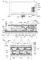
図1(A)は本発明の一態様の情報処理装置100の構成を説明するブロック図である。FIG. 1A is a block diagram illustrating a configuration of an information processing apparatus 100 according to an aspect of the present invention.
図1(B−1)および図1(B−2)は、本発明の一態様の情報処理装置100の構成を
説明する模式図である。1 (B-1) and 1 (B-2) are schematic views illustrating the configuration of the information processing apparatus 100 according to one aspect of the present invention.
図1(C−1)および図1(C−2)は、本発明の一態様の情報処理装置100が折り畳
まれる動作を説明する模式図である。1 (C-1) and 1 (C-2) are schematic views illustrating an operation in which the information processing apparatus 100 according to one aspect of the present invention is folded.
図2は本発明の一態様の情報処理装置100の演算部に実行させるプログラムを説明する
フロー図である。図2(A)は、主要な処理を説明するフロー図であり、図2(B)は、
割り込み処理を説明するフロー図である。FIG. 2 is a flow chart illustrating a program to be executed by the arithmetic unit of the information processing apparatus 100 according to one aspect of the present invention. FIG. 2A is a flow chart illustrating the main processing, and FIG. 2B is a flow diagram.
It is a flow diagram explaining interrupt processing.
本実施の形態で説明する情報処理装置100は、折り畳み情報SENSを供給し、画像情
報VIDEOが供給される入出力装置120と、折り畳み情報SENSが供給され、画像
情報VIDEOを供給する演算装置110と、を有する(図1(A)参照)。The information processing apparatus 100 described in the present embodiment includes an input /
入出力装置120は、展開された状態または2以上の異なる折り畳まれた状態にすること
ができる表示部122および表示部122の状態を検知して折り畳み情報SENSを供給
することができる検知部123を備える。The input /
演算装置110は、演算部111および演算部111に処理を実行させるプログラムを記
憶する記憶部112を備え、当該プログラムは、折り畳み情報SENSに応じて異なる処
理を演算部111に実行させる。The arithmetic unit 110 includes a
本実施の形態で説明する情報処理装置100は、展開および折り畳むことができる表示部
122並びにその状態を検知して折り畳み情報SENSを供給することができる検知部1
23を備える入出力装置120と、折り畳み情報SENSに応じて異なる処理を実行させ
るプログラムを記憶する演算装置110と、を含んで構成される。これにより、表示部1
22を展開して用いることができる。その結果、一覧性に優れた情報処理装置を提供する
ことができる。または、表示部122を折り畳むことができる。その結果、可搬性に優れ
た情報処理装置を提供することができる。The information processing apparatus 100 described in this embodiment has a
The input /
22 can be expanded and used. As a result, it is possible to provide an information processing apparatus having excellent listability. Alternatively, the
なお、本実施の形態で例示して説明する演算装置110は、入出力インターフェース11
5および伝送路114を備える(図1(A)参照)。The arithmetic unit 110 exemplified and described in this embodiment is an input / output interface 11.
5 and a transmission line 114 (see FIG. 1A).
入出力インターフェース115は、情報を入出力装置120に供給することができ、入出
力装置120から情報が供給される。The input /
伝送路114は、情報を演算部111、記憶部112および入出力インターフェース11
5に供給することができる。また、演算部111、記憶部112および入出力インターフ
ェース115は、情報を伝送路114に供給することができる。The
Can be supplied to 5. Further, the
入出力装置120は、入力手段121、標識129および通信部125等を備える。The input /
入力手段121は、終了命令を含む操作命令INPUT等を供給することができる。なお
、終了命令はプログラムを終了する命令である。The input means 121 can supply an operation instruction INPUT and the like including an end instruction. The end instruction is an instruction to end the program.
標識129は、表示部122の近傍に配置され、検知部123を用いて検知される。これ
により、表示部の折り畳まれた状態を知ることができる。The
なお、これらの構成は明確に分離できず、一つの構成が他の構成を兼ねる場合や他の構成
の一部を含む場合がある。例えば、表示部およびタッチセンサが重ねられたタッチパネル
は、表示部122であるとともに入力手段121でもある。It should be noted that these configurations cannot be clearly separated, and one configuration may serve as another configuration or may include a part of another configuration. For example, the touch panel on which the display unit and the touch sensor are superposed is not only the
また、本実施の形態で例示して説明する情報処理装置100は、以下のステップを含むプ
ログラムを記憶する記憶部112を備える(図2参照)。Further, the information processing apparatus 100 exemplified and described in the present embodiment includes a
《プログラム》
第1のステップにおいて、表示部122の折り畳まれた状態を折り畳み情報SENSから
特定する(図2(A)(S1)参照)。"program"
In the first step, the folded state of the
折り畳み情報SENSから表示部122の折り畳まれた状態を特定する方法については、
実施の形態2で詳細に説明する。For the method of specifying the folded state of the
This will be described in detail in the second embodiment.
第2のステップにおいて、折り畳まれた状態に割り当てられた処理用アプリケーションを
ロードする(図2(A)(S2)参照)。In the second step, the processing application assigned to the folded state is loaded (see FIGS. 2A and 2S).
なお、折り畳まれた状態に割り当てる処理用のアプリケーションとしては、例えば、情報
処理装置を、電子書籍の閲覧、音楽の再生、放送または動画の閲覧、ゲーム、カメラ等に
用いるためのアプリケーションを挙げることができる。Examples of the application for processing to be assigned to the folded state include an application for using an information processing device for browsing electronic books, playing music, watching broadcasts or videos, games, cameras, and the like. can.
第3のステップにおいて、割り込み処理を許可する(図2(A)(S3)参照)。In the third step, interrupt processing is permitted (see FIGS. 2A and 2S).
第4のステップにおいて、割り込み処理を実行し、且つ所定の情報を処理する(図2(A
)(S4)参照)。In the fourth step, interrupt processing is executed and predetermined information is processed (FIG. 2 (A).
) (S4).
なお、第4のステップでする情報の処理としては、例えば、記憶部112にある情報を入
出力装置120に出力する処理等を挙げることができる。具体的には、記憶部112に圧
縮されて記憶された画像情報を伸張して表示部122に表示する処理、圧縮されて記憶さ
れた音声情報を伸張してスピーカ等に出力する処理、文字情報をレイアウト情報に基づい
て調整して表示する処理などが挙げられる。Examples of the information processing performed in the fourth step include processing for outputting the information in the
第5のステップにおいて、終了命令が供給される場合は第6のステップに進み、終了命令
が供給されない場合は第1のステップに進む(図2(A)(S5)参照)。In the fifth step, if the end command is supplied, the process proceeds to the sixth step, and if the end command is not supplied, the process proceeds to the first step (see FIGS. 2A and 2S).
第6のステップにおいて、終了する(図2(A)(S6)参照)。The sixth step ends (see FIGS. 2 (A) and 2 (S6)).
割り込み処理について説明する(図2(B)参照)。なお、割り込み処理が許可された演
算部は、割り込み処理についての実行命令を受けつけることができる。そして、割り込み
処理についての実行命令を受けつけた演算部は、主の処理を中断し、割り込み処理を実行
する。例えば、割り込み処理についての実行命令に関連付けられたイベントを供給された
演算部は、割り込み処理を実行し、実行結果を記憶部に格納する。その後、割り込み処理
から主の処理に復帰した演算部は、主の処理を、割り込み処理の実行結果に基づいて再開
することができる。Interrupt processing will be described (see FIG. 2B). The arithmetic unit for which interrupt processing is permitted can receive an execution instruction for interrupt processing. Then, the arithmetic unit that receives the execution instruction for the interrupt processing interrupts the main processing and executes the interrupt processing. For example, the arithmetic unit supplied with the event associated with the execution instruction for the interrupt processing executes the interrupt processing and stores the execution result in the storage unit. After that, the arithmetic unit that has returned from the interrupt processing to the main processing can restart the main processing based on the execution result of the interrupt processing.
割り込み処理は、第7のステップにおいて、折り畳まれた状態を折り畳み情報SENSか
ら特定する(図2(B)(T7)参照)。In the interrupt processing, in the seventh step, the folded state is specified from the folding information SENS (see FIGS. 2B and T7).
第8のステップにおいて、折り畳まれた状態が変化した場合は第9のステップに進み、折
り畳まれた状態が変化していない場合は第10のステップに進む(図2(B)(T8)参
照)。In the eighth step, if the folded state has changed, the process proceeds to the ninth step, and if the folded state has not changed, the process proceeds to the tenth step (see FIGS. 2B and T8). ..
なお、折り畳まれた状態の変化は、第1のステップにおいて特定された折り畳まれた状態
と比較することにより判断することができる。The change in the folded state can be determined by comparing with the folded state specified in the first step.
第9のステップにおいて、アプリケーションを終了する(図2(B)(T9)参照)。In the ninth step, the application is terminated (see FIGS. 2B (T9)).
第10のステップにおいて、割り込み処理から復帰する(図2(B)(T10)参照)。In the tenth step, the interrupt processing is restored (see FIG. 2B (T10)).
以下に、本発明の一態様の情報処理装置100を構成する個々の要素について説明する。Hereinafter, individual elements constituting the information processing apparatus 100 according to one aspect of the present invention will be described.
《入出力装置》
入出力装置120は、入出力インターフェース115を介して伝送路114に接続される
。入出力装置120は外部の情報を情報処理装置100に供給することができる。また、
情報処理装置100の内部の情報を外部に供給することができる。<< Input / output device >>
The input /
Information inside the information processing apparatus 100 can be supplied to the outside.
《検知部および標識》
検知部123は、少なくとも表示部122の折り畳まれた状態を検知して折り畳み情報S
ENSを供給する。<< Detector and sign >>
The
Supply ENS.
検知部123は、表示部122の近傍に配置された標識129を検知するセンサを備える
。これにより、検知部123は、表示部122の折り畳まれた状態に応じた折り畳み信号
を供給することができる。The
標識129に用いることができるものは、例えば、突起物等の物の形状や配置、光、電波
または磁力等の電磁波等を挙げることができる。具体的には、異なる極性(例えば磁石の
S極とN極)を有するもの、異なる信号(例えば異なる方法で変調された電磁波)を有す
るもの等が挙げられる。Examples of the
検知部123に用いることができるセンサは、標識129を識別できるものを選択して用
いる。As the sensor that can be used for the
具体的には、標識129に形状または配置が異なる構造(例えば突起物)を用いる場合は
、その構造を識別できるように異なる形状または配置を備える開閉器等をセンサに用いる
ことができる。または、標識129に光を用いる場合は、光電変換素子等をセンサに用い
ることができる。または、標識129に電波を用いる場合は、アンテナ等をセンサに用い
ることができる。または、標識129に磁力を用いる場合は、磁気センサ等をセンサに用
いることができる。Specifically, when a structure having a different shape or arrangement (for example, a protrusion) is used for the
標識を検知したセンサが供給する信号から、表示部122の折り畳まれた状態を特定する
方法については、実施の形態2で詳細に説明する。A method of identifying the folded state of the
なお、検知部123は、加速度、方位、GPS(Global positioning
System)信号、温度または湿度等を検知して、その情報を供給してもよい。The
System) A signal, temperature, humidity, etc. may be detected and the information may be supplied.
《入力手段》
入力手段121として、さまざまなヒューマンインターフェース等を用いることができる
。具体的には、キーボード、マウス、タッチセンサ、マイクまたはカメラ等を用いること
ができる。特に、ポインタを用いる操作命令の供給方法は、直感的な操作を可能にするた
め便利である。<< Input means >>
Various human interfaces and the like can be used as the input means 121. Specifically, a keyboard, a mouse, a touch sensor, a microphone, a camera, or the like can be used. In particular, the method of supplying operation commands using pointers is convenient because it enables intuitive operations.
例えば、表示部に重ねて一体に設けられた入力手段121にタッチパネルを適用する場合
、情報処理装置100の使用者は、タッチパネルに触れた指をポインタに用いてするジェ
スチャー(タップ、ドラッグ、スワイプまたはピンチイン等)で、終了命令を含む操作命
令INPUT等を入力することができる。For example, when the touch panel is applied to the input means 121 integrally provided on the display unit, the user of the information processing apparatus 100 uses a finger touching the touch panel as a pointer (tap, drag, swipe, or gesture). It is possible to input an operation command INPUT or the like including an end command by pinching in or the like).
《表示部》
表示部122は可撓性を有する。表示部122は可撓性を有するため、折り畳むことがで
きる。《Display part》
The
表示部122が平面状に広げられた状態の第1の面(表面ともいう)を図1(B−1)に
示す。第1の面に対向する第2の面(裏面ともいう)を図1(B−2)に示す。FIG. 1 (B-1) shows a first surface (also referred to as a surface) in which the
表示部122が折り畳まれた状態を図1(C−1)および図1(C−2)に示す。The folded state of the
なお、本実施の形態に適用することができる可撓性を有する表示部の構成については、実
施の形態4または実施の形態5で詳細に説明する。The configuration of the flexible display unit applicable to the present embodiment will be described in detail in the fourth or fifth embodiment.
なお、本実施の形態で説明する情報処理装置100は、3つに折り畳むことができる表示
部122を備えるがこれに限られない。具体的には、表示部は、2つに折り畳むことがで
きる構成であっても、4つ以上に折り畳むことができる構成であってもよい。折り畳むこ
とができる数が多いほど、一覧性に優れた情報処理装置を提供することができる。または
、可搬性に優れた情報処理装置を提供することができる。The information processing apparatus 100 described in this embodiment includes, but is not limited to, a
《通信部》
通信部125は、外部のネットワークと情報処理装置100を接続する。情報処理装置1
00は、情報COMを外部から取得、または外部に供給することができる。具体的には、
ネットワーク接続機器またはモデム等を通信部125に用いることができる。<< Communication Department >>
The
00 can acquire the information COM from the outside or supply it to the outside. In particular,
A network connection device, a modem, or the like can be used for the
《その他》
入出力装置120として、例えばカメラ、マイク、読み取り専用の外部記憶部、外部記憶
部、通信機器、スキャナー、スピーカ、プリンタ等を用いることができる。"others"
As the input /
具体的には、カメラとして、デジタルカメラ、デジタルビデオカメラ等を用いることがで
きる。Specifically, as the camera, a digital camera, a digital video camera, or the like can be used.
外部記憶部としては、ハードディスク、リムーバブルメモリなどを用いることができる。
また、読み取り専用の外部記憶部としては、CDROM、DVDROMなどを用いること
ができる。As the external storage unit, a hard disk, a removable memory, or the like can be used.
Further, as the read-only external storage unit, a CDROM, a DVDROM, or the like can be used.
なお、本実施の形態は、本明細書で示す他の実施の形態と適宜組み合わせることができる
。It should be noted that this embodiment can be appropriately combined with other embodiments shown in the present specification.
(実施の形態2)
本実施の形態では、本発明の一態様の情報処理装置の構成について、図1および図3を参
照しながら説明する。(Embodiment 2)
In the present embodiment, the configuration of the information processing apparatus according to one aspect of the present invention will be described with reference to FIGS. 1 and 3.
具体的には、折り畳み可能な表示部122と、表示部122を支持する折り畳み可能な筐
体と、筐体に配置された標識129と、標識129を検知する検知部123と、を有する
情報処理装置100について説明する。また、情報処理装置100の折り畳まれた状態に
応じて検知部123が供給する折り畳み信号について、説明する。Specifically, information processing including a
図3は、本発明の一態様の情報処理装置100の表示部122およびそれを支持する筐体
が折り畳まれた状態を説明する模式図である。具体的には、展開された状態と10種類の
異なる折り畳まれた状態を説明する模式図である。FIG. 3 is a schematic diagram illustrating a state in which the
本実施の形態で説明する情報処理装置100は、第1の面(表面ともいう。図1(B−1
)参照)および第1の面に対向する第2の面(裏面ともいう。図1(B−2)参照)を備
える連結筐体Cを有する。The information processing apparatus 100 described in this embodiment has a first surface (also referred to as a surface, FIG. 1 (B-1).
) And a second surface facing the first surface (also referred to as a back surface; see FIG. 1 (B-2)).
また、情報処理装置100は、連結筐体Cの第1の面に近接することができる第1の標識
129(1)および第2の標識129(2)並びに第2の面に近接することができる第3
の標識129(3)および第4の標識129(4)を識別する検知部123を有する。な
お、検知部123は、センサ123Lを含む。Further, the information processing apparatus 100 may be close to the first label 129 (1) and the second marker 129 (2) and the second surface which can be close to the first surface of the connecting housing C. The third that can be done
It has a
また、情報処理装置100は、第1の面が連結筐体Cの第1の面に向き合う位置から第1
の面に対向する第2の面が連結筐体Cの第2の面に向き合う位置まで回動可能に、連結筐
体Cと接続される第1の筐体Lを有する(図1(C−1)参照)。Further, the information processing apparatus 100 is first from a position where the first surface faces the first surface of the connecting housing C.
Has a first housing L connected to the connecting housing C so that the second surface facing the surface of the connecting housing C can rotate to a position facing the second surface of the connecting housing C (FIG. 1 (C-). See 1)).
また、情報処理装置100は、第1の面が連結筐体Cの第1の面に向き合う位置から第1
の面に対向する第2の面が連結筐体Cの第2の面に向き合う位置まで回動可能に、連結筐
体Cと接続される第2の筐体Rを有する(図1(C−2)参照)。Further, the information processing apparatus 100 is first from a position where the first surface faces the first surface of the connecting housing C.
Has a second housing R connected to the connecting housing C so that the second surface facing the surface of the connecting housing C can rotate to a position facing the second surface of the connecting housing C (FIG. 1 (C-). 2)).
また、連結筐体C、第1の筐体Lおよび第2の筐体Rは、可撓性を有する表示部122を
折り畳み可能に支持する。Further, the connecting housing C, the first housing L and the second housing R support the
また、第1の筐体Lは、第1の標識129(1)を第1の面に、第3の標識129(3)
を第2の面に備える。Further, in the first housing L, the first sign 129 (1) is placed on the first surface, and the third sign 129 (3) is used.
Is prepared for the second surface.
また、第2の筐体Rは、第2の標識129(2)を第1の面に、第4の標識129(4)
を第2の面に備える。Further, the second housing R has the second sign 129 (2) on the first surface and the fourth sign 129 (4).
Is prepared for the second surface.
本実施の形態で説明する情報処理装置100は、展開および折り畳むことができる表示部
122並びにその状態を検知して折り畳み情報を供給することができる検知部123を備
える。これにより、一覧性に優れた情報処理装置を提供することができる。または、可搬
性に優れた情報処理装置を提供することができる。The information processing apparatus 100 described in this embodiment includes a
また、本実施の形態で説明する情報処理装置100は、第2の筐体Rが、第5の標識12
9(5)を第1の面に、第6の標識129(6)を第2の面に備える。また、検知部12
3が、第1の筐体Lの第1の面に近接する第6の標識129(6)並びに第1の筐体Lの
第2の面に近接する第5の標識129(5)を識別する。なお、検知部123は、センサ
123Uを含む。Further, in the information processing apparatus 100 described in the present embodiment, the second housing R is the fifth marker 12.
A 9 (5) is provided on the first surface and a sixth marker 129 (6) is provided on the second surface. Further, the detection unit 12
3 identifies a sixth sign 129 (6) close to the first surface of the first housing L and a fifth sign 129 (5) close to the second surface of the first housing L. do. The
本実施の形態で説明する情報処理装置100は、表示部122の展開または折り畳まれた
状態を検知して折り畳み情報SENSを供給することができる。具体的には、情報処理装
置100を展開された状態または10種類の折り畳まれた状態にすることができ、検知部
はその状態毎に異なる折り畳み情報SENSを供給することができる。これにより、異な
る処理を実行させるプログラムを11種類の状態毎に割り当てることができる。その結果
、折り畳む方法を変えることにより、簡単に多様な機能を選択して使用することができる
情報処理装置を提供できる。The information processing apparatus 100 described in this embodiment can detect the expanded or folded state of the
情報処理装置100の表示部122の2以上の異なる折り畳まれた状態を、図3を用いて
説明する。Two or more different folded states of the
検知部123は、センサ123Lを連結筐体Cに備え、センサ123Uを第1の筐体Lに
備える。なお、センサ123Lおよびセンサ123Uは、いずれも第1の面に近接する標
識129と第2の面に近接する標識129を識別することができる。The
検知部123は、センサ123Lおよびセンサ123Uが供給する信号の組み合わせから
、表示部122の折り畳まれた状態を特定することができる折り畳み情報SENSを生成
して供給する。The
なお、センサ123Lおよびセンサ123Uは、第1の面に標識129(x)が近接し、
第2の面に標識129(y)が近接した場合に、信号(x,y)を供給するものとする。
また、標識129が近接しない状態では信号(0,0)を供給するものとする。なお、こ
の表記は説明の便宜のためのものであり、信号の形式は近接する標識129が識別できる
ものであればこれに限定されない。In the
It is assumed that the signal (x, y) is supplied when the sign 129 (y) is close to the second surface.
Further, it is assumed that the signal (0,0) is supplied when the
<展開された状態>
情報処理装置100の連結筐体C、第1の筐体Lおよび第2の筐体Rが、展開された状態
を図3(A−1)および図3(A−2)に示す。なお、図3(A−1)は第1の面(表面
ともいう)から見た模式図であり、図3(A−2)は第1の面と対向する第2の面(裏面
ともいう)から見た模式図である。<Expanded state>
FIGS. 3 (A-1) and 3 (A-2) show the expanded states of the connecting housing C, the first housing L, and the second housing R of the information processing apparatus 100. Note that FIG. 3 (A-1) is a schematic view seen from the first surface (also referred to as a front surface), and FIG. 3 (A-2) is a second surface (also referred to as a back surface) facing the first surface. ) Is a schematic diagram.
なお、煩雑な図が発明の理解を妨げないように、図3(B−1)乃至図3(F−2)にお
いて、標識129(1)乃至標識129(6)、表示部122、センサ123Lおよびセ
ンサ123Uを省略する。これらの図は、図3(A−1)および図3(A−2)と対比し
て参照することにより、当業者であれば容易に理解することができる。In addition, in FIGS. 3 (B-1) to 3 (F-2), the signs 129 (1) to 129 (6), the
情報処理装置100の連結筐体C、第1の筐体Lおよび第2の筐体Rが、展開された状態
において、センサ123Uおよびセンサ123Lはいずれの標識も検知しない。これによ
り、センサ123Uは信号(0,0)を供給し、センサ123Lは信号(0,0)を供給
する。When the connected housing C, the first housing L, and the second housing R of the information processing apparatus 100 are deployed, the
<2つ折りにされた状態>
情報処理装置100の第1の筐体Lが第2の面に折り畳まれた場合、センサ123Lは、
第1の筐体Lの第2の面に配置された第3の標識129(3)を検知し、信号(0,3)
を供給する(図3(B−1)参照)。<Folded in half>
When the first housing L of the information processing apparatus 100 is folded to the second surface, the
The third sign 129 (3) arranged on the second surface of the first housing L is detected, and the signal (0, 3) is detected.
(See FIG. 3 (B-1)).
情報処理装置100の第1の筐体Lが第1の面に折り畳まれた場合、センサ123Lは、
第1の筐体Lの第1の面に配置された第1の標識129(1)を検知し、信号(1,0)
を供給する(図3(B−2)参照)。When the first housing L of the information processing apparatus 100 is folded to the first surface, the
The first sign 129 (1) arranged on the first surface of the first housing L is detected, and the signal (1,0) is detected.
(See FIG. 3 (B-2)).
情報処理装置100の第2の筐体Rが第2の面に折り畳まれた場合、センサ123Lは、
第2の筐体Rの第2の面に配置された第4の標識129(4)を検知し、信号(0,4)
を供給する(図3(C−1)参照)。When the second housing R of the information processing apparatus 100 is folded to the second surface, the
The fourth sign 129 (4) arranged on the second surface of the second housing R is detected, and the signal (0, 4) is detected.
(See FIG. 3 (C-1)).
情報処理装置100の第2の筐体Rが第1の面に折り畳まれた場合、センサ123Lは、
第2の筐体Rの第1の面に配置された第2の標識129(2)を検知し、信号(2,0)
を供給する(図3(C−2)参照)。When the second housing R of the information processing apparatus 100 is folded to the first surface, the
The second sign 129 (2) arranged on the first surface of the second housing R is detected, and the signal (2,0) is detected.
(See FIG. 3 (C-2)).
なお、2つ折りの状態において、センサ123Uはいずれの標識も検知しない。これによ
り、センサ123Uは信号(0,0)を供給する。In the folded state, the
<3つ折りにされた状態>
情報処理装置100の第1の筐体Lが第2の面に折り畳まれ、且つ第2の筐体Rが第1の
面に折り畳まれた場合、センサ123Lは、第1の筐体Lの第2の面に配置された第3の
標識129(3)および第2の筐体Rの第1の面に配置された第2の標識129(2)を
検知し、信号(2,3)を供給する(図3(D−1)参照)。<Folded in three>
When the first housing L of the information processing apparatus 100 is folded to the second surface and the second housing R is folded to the first surface, the
なお、連結筐体Cは、第1の筐体Lに配置されたセンサ123Uと第2の筐体Rの第1の
面に配置された第5の標識129(5)の間にある。これにより、センサ123Uは信号
(0,0)を供給する。The connecting housing C is located between the
情報処理装置100の第1の筐体Lが第1の面に折り畳まれ、且つ第2の筐体Rが第2の
面に折り畳まれた場合、センサ123Lは、第1の筐体Lの第1の面に配置された第1の
標識129(1)および第2の筐体Rの第2の面に配置された第4の標識129(4)を
検知し、信号(1,4)を供給する(図3(D−2)参照)。When the first housing L of the information processing apparatus 100 is folded to the first surface and the second housing R is folded to the second surface, the
なお、連結筐体Cが、第1の筐体Lに配置されたセンサ123Uと第2の筐体Rの第2の
面に配置された第6の標識129(6)の間にある。これにより、センサ123Uは信号
(0,0)を供給する。The connecting housing C is located between the
情報処理装置100の第1の筐体Lが第2の面に折り畳まれ、第1の筐体Lに重ねて第2
の筐体Rが第2の面に折り畳まれた場合、センサ123Lは、第1の筐体Lの第2の面に
配置された第3の標識129(3)を検知し、信号(0,3)を供給する(図3(E−1
)参照)。また、センサ123Uは、第2の筐体Rの第2の面に配置された第6の標識1
29(6)を検知し、信号(6,0)を供給する。The first housing L of the information processing apparatus 100 is folded on the second surface and overlapped with the first housing L.
When the housing R of the housing R is folded to the second surface, the
)reference). Further, the
29 (6) is detected and a signal (6,0) is supplied.
情報処理装置100の第2の筐体Rが第2の面に折り畳まれ、第2の筐体Rに重ねて第1
の筐体Lが第2の面に折り畳まれた場合、センサ123Lは、第2の筐体Rの第2の面に
配置された第4の標識129(4)を検知し、信号(0,4)を供給する(図3(E−2
)参照)。また、センサ123Uは、第2の筐体Rの第1の面に配置された第5の標識1
29(5)を検知し、信号(0,5)を供給する。The second housing R of the information processing apparatus 100 is folded on the second surface and overlapped with the second housing R.
When the housing L of the housing L is folded to the second surface, the
)reference). Further, the
29 (5) is detected and a signal (0, 5) is supplied.
情報処理装置100の第1の筐体Lが第1の面に折り畳まれ、第1の筐体Lに重ねて第2
の筐体Rが第1の面に折り畳まれた場合、センサ123Lは、第1の筐体Lの第1の面に
配置された第1の標識129(1)を検知し、信号(1,0)を供給する(図3(F−1
)参照)。また、センサ123Uは、第2の筐体Rの第1の面に配置された第5の標識1
29(5)を検知し、信号(0,5)を供給する。The first housing L of the information processing apparatus 100 is folded on the first surface and overlapped with the first housing L to form a second housing L.
When the housing R of the housing R is folded to the first surface, the
)reference). Further, the
29 (5) is detected and a signal (0, 5) is supplied.
情報処理装置100の第2の筐体Rが第1の面に折り畳まれ、第2の筐体Rに重ねて第1
の筐体Lが第1の面に折り畳まれた場合、センサ123Lは、第2の筐体Rの第1の面に
配置された第2の標識129(2)を検知し、信号(2,0)を供給する(図3(F−2
)参照)。また、センサ123Uは、第2の筐体Rの第2の面に配置された第6の標識1
29(6)を検知し、信号(6,0)を供給する。The second housing R of the information processing apparatus 100 is folded on the first surface and overlapped with the second housing R.
When the housing L of the housing L is folded to the first surface, the
)reference). Further, the
29 (6) is detected and a signal (6,0) is supplied.
なお、本実施の形態は、本明細書で示す他の実施の形態と適宜組み合わせることができる
。It should be noted that this embodiment can be appropriately combined with other embodiments shown in the present specification.
(実施の形態3)
本実施の形態では、本発明の一態様の情報処理装置200の構成について、図4乃至図7
を参照しながら説明する。(Embodiment 3)
In the present embodiment, FIGS. 4 to 7 show the configuration of the
Will be explained with reference to.
図4(A)は、展開された状態の本発明の一態様の情報処理装置200の構造を説明する
上面図であり、図4(B)はその側面図である。FIG. 4A is a top view illustrating the structure of the
図5(A)は、2つに折り畳まれた状態の本発明の一態様の情報処理装置200の構造を
説明する上面図であり、図5(B)はその側面図である。また、図5(C)は、図5(A
)とは異なる方法で2つに折り畳まれた本発明の一態様の情報処理装置200の構造を説
明する上面図であり、図5(D)はその側面図である。FIG. 5A is a top view illustrating the structure of the
It is a top view illustrating the structure of the
図6(A)は、図5(A)と図5(C)とは異なる方法で2つに折り畳まれた本発明の一
態様の情報処理装置200の構造を説明する上面図であり、図6(B)はその側面図であ
る。また、図6(C)は、図6(A)とは異なる方法で2つに折り畳まれた本発明の一態
様の情報処理装置200の構造を説明する上面図であり、図6(D)はその側面図である
。6 (A) is a top view illustrating the structure of the
図7(A−1)は、3つに折り畳まれた本発明の一態様の情報処理装置200の構造を説
明する上面図であり、図7(A−2)はその側面図である。FIG. 7 (A-1) is a top view illustrating the structure of the
図7(B−1)は、図7(A−1)とは異なる方法で3つに折り畳まれた本発明の一態様
の情報処理装置200の構造を説明する上面図であり、図7(B−2)はその側面図であ
る。FIG. 7 (B-1) is a top view illustrating the structure of the
図7(C−1)は、図7(A−1)および図7(B−1)とは異なる方法で3つに折り畳
まれた本発明の一態様の情報処理装置200の構造を説明する上面図であり、図7(C−
2)はその側面図である。FIG. 7 (C-1) describes the structure of the
2) is a side view thereof.
本実施の形態で例示して説明する情報処理装置200は、連結筐体Cを有する。連結筐体
Cは、近接する標識を識別するセンサ123Lを備える(図4(A)参照)。The
情報処理装置200は、第1の筐体Lを有する。第1の筐体Lは、連結筐体Cとリンク2
11を介して連結されている。これにより、第1の筐体Lは、第1の面が連結筐体Cの第
1の面に向き合う位置から、第1の面に対向する第2の面が連結筐体Cの第2の面に向き
合う位置まで回動することができる(図4(B)参照)。その結果、情報処理装置200
は折り畳むことができる。The
It is connected via 11. As a result, in the first housing L, the second surface facing the first surface is the second surface of the connecting housing C from the position where the first surface faces the first surface of the connecting housing C. It can rotate to a position facing the surface (see FIG. 4B). As a result, the
Can be folded.
また、第1の筐体Lは、センサ123Uを備える。また、第1の筐体Lは、第1の標識1
29(1)を第1の面に、第3の標識129(3)を第2の面に備える。Further, the first housing L includes a
29 (1) is provided on the first surface and a third marker 129 (3) is provided on the second surface.
情報処理装置200は、第2の筐体Rを有する。第2の筐体Rは、連結筐体Cとリンク2
12を介して連結されている。これにより、第2の筐体Rは、第1の面が連結筐体Cの第
1の面に向き合う位置から、第1の面に対向する第2の面が連結筐体Cの第2の面に向き
合う位置まで回動することができる。その結果、情報処理装置200は折り畳むことがで
きる。The
It is connected via 12. As a result, in the second housing R, the second surface facing the first surface is the second surface of the connecting housing C from the position where the first surface faces the first surface of the connecting housing C. It can rotate to a position facing the surface. As a result, the
また、第2の筐体Rは、第2の標識129(2)および第5の標識129(5)を第1の
面に、第4の標識129(4)および第6の標識129(6)を第2の面に備える。Further, the second housing R has the second label 129 (2) and the fifth label 129 (5) on the first surface, and the fourth label 129 (4) and the sixth label 129 (6). ) Is provided on the second surface.
情報処理装置200は、センサ123Lとセンサ123Uを含む検知部を備える。The
センサ123Lは、連結筐体Cの第1の面に近接する第1の標識129(1)および第2
の標識129(2)を識別し、第2の面に近接する第3の標識129(3)および第4の
標識129(4)を識別する。The
129 (2) of the third label 129 (3) and the fourth label 129 (4) adjacent to the second surface are identified.
センサ123Uは、第1の筐体の第1の面に近接する第6の標識129(6)および第2
の面に近接する第5の標識129(5)を識別する。The
Identifies a fifth marker 129 (5) in close proximity to the plane of.
情報処理装置200の連結筐体C、第1の筐体Lおよび第2の筐体Rは、可撓性を有する
表示部222を支持する。なお、図中の矢印は表示部222が画像を表示する方向を示す
。The connecting housing C, the first housing L, and the second housing R of the
本実施の形態で説明する情報処理装置200は、展開および折り畳むことができる表示部
222並びにその状態を検知して折り畳み情報を供給することができる検知部123を備
える。これにより、一覧性に優れた情報処理装置を提供することができる。または、可搬
性に優れた情報処理装置を提供することができる。The
<展開された状態>
情報処理装置200の連結筐体C、第1の筐体Lおよび第2の筐体Rが、展開された状態
において、センサ123Uおよびセンサ123Lはいずれの標識も検知しない。これによ
り、センサ123Uは信号(0,0)を供給し、センサ123Lは信号(0,0)を供給
する(図4(A)参照)。<Expanded state>
When the connected housing C, the first housing L, and the second housing R of the
<2つ折りにされた状態>
情報処理装置200の第1の筐体Lが第1の面に折り畳まれた場合、センサ123Lは、
第1の筐体Lの第1の面に配置された第1の標識129(1)を検知し、信号(0,1)
を供給する(図5(A)および図5(B)参照)。<Folded in half>
When the first housing L of the
The first sign 129 (1) arranged on the first surface of the first housing L is detected, and the signal (0, 1) is detected.
(See FIGS. 5 (A) and 5 (B)).
情報処理装置200は、図5(A)および図5(B)に示すように、第1の筐体Lを第1
の面に折り畳み、第1の筐体Lの第2の面および第2の筐体Rの第1の面を使用者に向け
て使用することができる。As shown in FIGS. 5A and 5B, the
The second surface of the first housing L and the first surface of the second housing R can be used toward the user.
なお、第1の筐体Lの第2の面に入力手段(例えばキーボード121K)を設けることが
できる(図5(A)参照)。An input means (for example, a
例えば、この状態に折り畳まれた場合に検知部が供給する折り畳み信号を、電子メールを
処理するアプリケーションに関連付けることができる。これにより、使用者は情報処理装
置200を図5(A)および図5(B)に示すように折り畳むことにより、電子メールを
処理することができる。具体的には、第2の筐体Rに支持された部分の表示部222を使
用しながら、文字情報等をキーボード121Kから入力することができる。また、第1の
筐体Lと連結筐体Cに支持された部分の表示部222の表示を停止して、消費電力を低減
することができる。For example, the folding signal supplied by the detector when folded in this state can be associated with an application that processes e-mail. Thereby, the user can process the e-mail by folding the
情報処理装置200の第1の筐体Lが第2の面に折り畳まれた場合、センサ123Lは、
第1の筐体Lの第2の面に配置された第3の標識129(3)を検知し、信号(0,3)
を供給する(図5(C)および図5(D)参照)。When the first housing L of the
The third sign 129 (3) arranged on the second surface of the first housing L is detected, and the signal (0, 3) is detected.
(See FIGS. 5 (C) and 5 (D)).
図5(C)および図5(D)に示すように第1の筐体Lを第2の面に折り畳むことにより
、情報処理装置200を連結筐体Cおよび第2の筐体Rの第1の面を使用者に向けて使用
することができる。By folding the first housing L to the second surface as shown in FIGS. 5C and 5D, the
例えば、この状態に折り畳まれた場合に検知部が供給する折り畳み信号を、電子書籍の閲
覧をするためのアプリケーションに関連付けることができる。これにより、使用者は情報
処理装置200を図5(C)および図5(D)に示すように折り畳むことにより、電子書
籍を閲覧することができる。For example, the folding signal supplied by the detector when folded in this state can be associated with an application for browsing an electronic book. As a result, the user can browse the electronic book by folding the
また、この状態に折り畳まれた情報処理装置200の表示部222のうち、第1の筐体L
に支持された部分は、使用者に向けられていないため、表示を停止することができる。こ
れにより、消費電力を低減することができる。Further, among the
Since the part supported by is not directed to the user, the display can be stopped. As a result, power consumption can be reduced.
表示部222の使用者に向けられていない部分にタッチパネルが重ねて設けられている場
合は、当該部分のタッチパネルを入力手段に用いてもよい。これにより、情報処理装置2
00を、使用者側にある親指と使用者に向けられていない側にある指で支持し、また操作
することができる。When the touch panel is provided on the portion of the
00 can be supported and operated with the thumb on the user side and the finger on the side not facing the user.
情報処理装置200の第2の筐体Rが第1の面に折り畳まれた場合、センサ123Lは、
第2の筐体Rの第1の面に配置された第2の標識129(2)を検知し、信号(0,2)
を供給する(図6(A)および図6(B)参照)。When the second housing R of the
The second sign 129 (2) arranged on the first surface of the second housing R is detected, and the signal (0, 2) is detected.
(See FIGS. 6 (A) and 6 (B)).
なお、第2の筐体Rの第2の面に入力手段(例えばコントロールボタン121B)を設け
ることができる(図6(A)参照)。An input means (for example,
例えば、この状態に折り畳まれた場合に検知部が供給する折り畳み信号を、ゲームのアプ
リケーションに関連付けることができる。これにより、使用者は情報処理装置200を図
6(A)および図6(B)に示すように折り畳むことにより、ゲームをすることができる
。具体的には、第1の筐体Lに支持された部分の表示部222を使用しながら、キャラク
ター等の操作をコントロールボタン121Bから入力することができる。また、第2の筐
体Rと連結筐体Cに支持された部分の表示部222の表示を停止して、消費電力を低減す
ることができる。For example, a folding signal supplied by the detector when folded in this state can be associated with a game application. As a result, the user can play the game by folding the
情報処理装置200の第2の筐体Rが第1の面に折り畳まれた場合、センサ123Rは、
第2の筐体Rの第2の面に配置された第4の標識129(4)を検知し、信号(0,4)
を供給する(図6(C)および図6(D)参照)。When the second housing R of the
The fourth sign 129 (4) arranged on the second surface of the second housing R is detected, and the signal (0, 4) is detected.
(See FIGS. 6 (C) and 6 (D)).
例えば、この状態に折り畳まれた場合に検知部が供給する折り畳み信号を、インターネッ
トのウエブサイトを閲覧するためのアプリケーションに関連付けることができる。これに
より、使用者は情報処理装置200を図6(C)および図6(D)に示すように折り畳む
ことにより、ウエブサイトを閲覧することができる。For example, the folding signal supplied by the detector when folded in this state can be associated with an application for browsing an Internet website. As a result, the user can browse the website by folding the
なお、図5に示すように折り畳まれた情報処理装置200に割り当てるアプリケーション
と、図6に示すように折り畳まれた情報処理装置200に割り当てるアプリケーションを
、使用者が選択できるようにしてもよい。例えば、使用者が右利きか、左利きかによって
、割り当てるアプリケーションを変えてもよい。The user may be able to select an application to be assigned to the folded
<3つ折りにされた状態>
情報処理装置200の第1の筐体Lが第2の面に折り畳まれ、第1の筐体Lに重ねて第2
の筐体Rが第2の面に折り畳まれた場合、センサ123Lは、第1の筐体Lの第2の面に
配置された第3の標識129(3)を検知し、信号(0,3)を供給する(図7(A−1
)および図7(A−2)参照)。また、図示されていないセンサ123Uは、第2の筐体
Rの第2の面に配置された第6の標識129(6)を検知し、信号(6,0)を供給する
。<Folded in three>
The first housing L of the
When the housing R of the housing R is folded to the second surface, the
) And FIG. 7 (A-2)). Further, the
情報処理装置200の第1の筐体Lが第2の面に折り畳まれ、且つ第2の筐体Rが第1の
面に折り畳まれた場合、センサ123Lは、第1の筐体Lの第2の面に配置された第3の
標識129(3)および第2の筐体Rの第1の面に配置された第2の標識129(2)を
検知し、信号(2,3)を供給する(図7(B−1)および図7(B−2)参照)。また
、図示されていないが、連結筐体Cが、第1の筐体Lに設けられたセンサ123Uと第2
の筐体Rの第1の面に設けられた第5の標識129(5)の間にある。これにより、セン
サ123Uは信号(0,0)を供給する。When the first housing L of the
It is between the fifth sign 129 (5) provided on the first surface of the housing R of the above. As a result, the
なお、第2の筐体Rの第2の面に入力手段(例えばカメラ121C)を設けることができ
る(図7(B−1)参照)。An input means (for example, camera 121C) can be provided on the second surface of the second housing R (see FIG. 7 (B-1)).
例えば、この状態に折り畳まれた場合に検知部が供給する折り畳み信号を、映像を取り込
むアプリケーションに関連付けることができる。これにより、使用者は情報処理装置20
0を図7(B−1)および図7(B−2)に示すように折り畳むことにより、映像を取り
込むことができる。具体的には、第1の筐体Lに支持された部分の表示部222を使用し
ながら、映像をカメラ121Cから取り込むことができる。また、第2の筐体Rと連結筐
体Cに支持された部分の表示部222の表示を停止して、消費電力を低減することができ
る。For example, the folding signal supplied by the detector when folded in this state can be associated with an application that captures video. As a result, the user can use the information processing device 20.
Images can be captured by folding 0 as shown in FIGS. 7 (B-1) and 7 (B-2). Specifically, the image can be captured from the camera 121C while using the
情報処理装置200の第2の筐体Rが第1の面に折り畳まれ、第2の筐体Rに重ねて第1
の筐体Lが第1の面に折り畳まれた場合、センサ123Lは、第2の筐体Rの第1の面に
配置された第2の標識129(2)を検知し、信号(2,0)を供給する(図7(C−1
)および図7(C−2)参照)。また、センサ123Uは、第2の筐体Rの第2の面に配
置された第6の標識129(6)を検知し、信号(6,0)を供給する。The second housing R of the
When the housing L of the housing L is folded to the first surface, the
) And FIG. 7 (C-2)). Further, the
例えば、この状態に折り畳まれた場合に検知部が供給する折り畳み信号を、情報処理装置
を待機状態に移行させる命令と関連付けることができる。これにより、使用者は情報処理
装置200を図7(C−1)および図7(C−2)に示すように折り畳むことにより、表
示部222の表示を停止して、消費電力を低減することができる。For example, the folding signal supplied by the detection unit when folded in this state can be associated with an instruction to shift the information processing apparatus to the standby state. As a result, the user can fold the
なお、本実施の形態は、本明細書で示す他の実施の形態と適宜組み合わせることができる
。It should be noted that this embodiment can be appropriately combined with other embodiments shown in the present specification.
(実施の形態4)
本実施の形態では、本発明の一態様の情報処理装置に適用することができる入出力装置の
構成について、図8を参照しながら説明する。(Embodiment 4)
In the present embodiment, the configuration of the input / output device that can be applied to the information processing device of one aspect of the present invention will be described with reference to FIG.
図8(A)は本発明の一態様の情報処理装置に適用可能な入出力装置の構造を説明する上
面図である。FIG. 8A is a top view illustrating the structure of the input / output device applicable to the information processing device of one aspect of the present invention.
図8(B)は図8(A)の切断線A−Bおよび切断線C−Dにおける断面図である。8 (B) is a cross-sectional view taken along the cutting line AB and the cutting line CD of FIG. 8 (A).
図8(C)は図8(A)の切断線E−Fにおける断面図である。8 (C) is a cross-sectional view taken along the cutting line EF of FIG. 8 (A).
<上面図の説明>
本実施の形態で例示する入出力装置300は表示部301を有する(図8(A)参照)。<Explanation of top view>
The input /
表示部301は、複数の画素302と複数の撮像画素308を備える。撮像画素308は
表示部301に触れる指等を検知することができる。これにより、撮像画素308を用い
てタッチセンサを構成することができる。The
画素302は、複数の副画素(例えば副画素302R)を備え、副画素は発光素子および
発光素子を駆動する電力を供給することができる画素回路を備える。The
画素回路は、選択信号を供給することができる配線および画像信号を供給することができ
る配線と、電気的に接続される。The pixel circuit is electrically connected to a wiring capable of supplying a selection signal and a wiring capable of supplying an image signal.
また、入出力装置300は選択信号を画素302に供給することができる走査線駆動回路
303g(1)と、画像信号を画素302に供給することができる画像信号線駆動回路3
03s(1)を備える。なお、折り曲げられる部分を避けて画像信号線駆動回路303s
(1)を配置すると、不具合の発生を低減できる。Further, the input /
03s (1) is provided. The image signal
By arranging (1), the occurrence of defects can be reduced.
撮像画素308は、光電変換素子および光電変換素子を駆動する撮像画素回路を備える。The
撮像画素回路は、制御信号を供給することができる配線および電源電位を供給することが
できる配線と電気的に接続される。The image pickup pixel circuit is electrically connected to a wiring capable of supplying a control signal and a wiring capable of supplying a power supply potential.
制御信号としては、例えば記録された撮像信号を読み出す撮像画素回路を選択することが
できる信号、撮像画素回路を初期化することができる信号、および撮像画素回路が光を検
知する時間を決定することができる信号などを挙げることができる。As the control signal, for example, a signal capable of selecting an image pickup pixel circuit for reading the recorded image pickup signal, a signal capable of initializing the image pickup pixel circuit, and a time for the image pickup pixel circuit to detect light are determined. Can be mentioned as a signal that can be generated.
入出力装置300は制御信号を撮像画素308に供給することができる撮像画素駆動回路
303g(2)と、撮像信号を読み出す撮像信号線駆動回路303s(2)を備える。な
お、撮像信号線駆動回路303s(2)を折り曲げられる部分を避けて配置すると、不具
合の発生を低減できる。The input /
<断面図の説明>
入出力装置300は、基板310および基板310に対向する対向基板370を有する(
図8(B)参照)。<Explanation of cross section>
The input /
See FIG. 8 (B)).
基板310は、可撓性を有する基板310b、意図しない不純物の発光素子への拡散を防
ぐバリア膜310aおよび基板310bとバリア膜310aを貼り合わせる接着層310
cが積層された積層体である。The
It is a laminated body in which c is laminated.
対向基板370は、可撓性を有する基板370b、意図しない不純物の発光素子への拡散
を防ぐバリア膜370aおよび基板370bとバリア膜370aを貼り合わせる接着層3
70cの積層体である(図8(B)参照)。The facing
It is a laminated body of 70c (see FIG. 8B).
封止材360は対向基板370と基板310を貼り合わせている。また、封止材360は
空気より大きい屈折率を備え、光学接合層を兼ねる。画素回路および発光素子(例えば第
1の発光素子350R)並びに撮像画素回路および光電変換素子(例えば光電変換素子3
08p)は基板310と対向基板370の間にある。As the sealing
08p) is between the
《画素の構成》
画素302は、副画素302R、副画素302Gおよび副画素302Bを有する(図8(
C)参照)。また、副画素302Rは発光モジュール380Rを備え、副画素302Gは
発光モジュール380Gを備え、副画素302Bは発光モジュール380Bを備える。<< Pixel composition >>
The
See C). Further, the sub-pixel 302R includes a
例えば副画素302Rは、第1の発光素子350Rおよび第1の発光素子350Rに電力
を供給することができるトランジスタ302tを含む画素回路を備える(図8(B)参照
)。また、発光モジュール380Rは第1の発光素子350Rおよび光学素子(例えば第
1の着色層367R)を備える。For example, the sub-pixel 302R includes a pixel circuit including a
発光素子350Rは、第1の下部電極351R、上部電極352、下部電極351Rと上
部電極352の間に発光性の有機化合物を含む層353を有する(図8(C)参照)。The
発光性の有機化合物を含む層353は、発光ユニット353a、発光ユニット353bお
よび発光ユニット353aと発光ユニット353bの間に中間層354を備える。The layer 353 containing the luminescent organic compound includes a light emitting unit 353a, a
発光モジュール380Rは、第1の着色層367Rを対向基板370に有する。着色層は
特定の波長を有する光を透過するものであればよく、例えば赤色、緑色または青色等を呈
する光を選択的に透過するものを用いることができる。または、発光素子の発する光をそ
のまま透過する領域を設けてもよい。The
例えば、発光モジュール380Rは、第1の発光素子350Rと第1の着色層367Rに
接する封止材360を有する。For example, the
第1の着色層367Rは第1の発光素子350Rと重なる位置にある。これにより、発光
素子350Rが発する光の一部は、光学接合層を兼ねる封止材360および第1の着色層
367Rを透過して、図中の矢印に示すように発光モジュール380Rの外部に射出され
る。The first
《入出力装置の構成》
入出力装置300は、遮光層367BMを対向基板370に有する。遮光層367BMは
、着色層(例えば第1の着色層367R)を囲むように設けられている。<< Configuration of input / output device >>
The input /
入出力装置300は、反射防止層367pを表示部301に重なる位置に備える。反射防
止層367pとして、例えば円偏光板を用いることができる。The input /
入出力装置300は、絶縁膜321を備える。絶縁膜321はトランジスタ302tを覆
っている。なお、絶縁膜321は画素回路に起因する凹凸を平坦化するための層として用
いることができる。また、不純物のトランジスタ302t等への拡散を抑制することがで
きる層が積層された絶縁膜を、絶縁膜321に適用することができる。The input /
入出力装置300は、発光素子(例えば第1の発光素子350R)を絶縁膜321上に有
する。The input /
入出力装置300は、第1の下部電極351Rの端部に重なる隔壁328を絶縁膜321
上に有する(図8(C)参照)。また、基板310と対向基板370の間隔を制御するス
ペーサ329を、隔壁328上に有する。The input /
Have on top (see FIG. 8 (C)). Further, a
《画像信号線駆動回路の構成》
画像信号線駆動回路303s(1)は、トランジスタ303tおよび容量303cを含む
。なお、画像信号線駆動回路303s(1)は画素回路と同一の工程で同一基板上に形成
することができる。<< Configuration of image signal line drive circuit >>
The image signal
《撮像画素の構成》
撮像画素308は、光電変換素子308pおよび光電変換素子308pに照射された光を
検知するための撮像画素回路を備える。また、撮像画素回路は、トランジスタ308tを
含む。<< Configuration of imaging pixels >>
The
例えばpin型のフォトダイオードを光電変換素子308pに用いることができる。For example, a pin type photodiode can be used for the
《他の構成》
入出力装置300は、信号を供給することができる配線311を備え、端子319が配線
311に設けられている。なお、画像信号および同期信号等の信号を供給することができ
るFPC309(1)が端子319に電気的に接続されている。また、好ましくは、入出
力装置300の折り曲げられる部分を避けてFPC309(1)を配置する。また、表示
部301を囲む領域から選ばれた一辺、特に折り畳まれる辺(図では長い辺)のおよそ中
央にFPC309(1)を配置すると好ましい。これにより、入出力装置300と入出力
装置300を駆動する外部回路の距離を短くすることができ、接続が容易になる。また、
外部回路の重心を入出力装置300の重心におよそ一致させることができる。その結果、
情報処理装置の取り扱いが容易になり、誤って落としてしまう等の不具合の発生を予防す
ることができる。<< Other configurations >>
The input /
The center of gravity of the external circuit can be made to approximately match the center of gravity of the input /
The information processing device can be easily handled, and problems such as accidental dropping can be prevented.
なお、FPC309(1)にはプリント配線基板(PWB)が取り付けられていても良い
。A printed wiring board (PWB) may be attached to the FPC 309 (1).
なお、本実施の形態は、本明細書で示す他の実施の形態と適宜組み合わせることができる
。It should be noted that this embodiment can be appropriately combined with other embodiments shown in the present specification.
(実施の形態5)
本実施の形態では、入力手段としてタッチセンサ(接触検出装置)が表示部に重ねて設け
られ、折り曲げることができるタッチパネルの構成について、図9及び図10を参照しな
がら説明する。(Embodiment 5)
In the present embodiment, a touch panel (contact detection device) is provided on the display unit as an input means, and a structure of a touch panel that can be bent will be described with reference to FIGS. 9 and 10.
図9(A)は、本実施の形態で例示するタッチパネル500の斜視概略図である。なお明
瞭化のため、代表的な構成要素を図9に示す。図9(B)は、タッチパネル500を展開
した斜視概略図である。FIG. 9A is a schematic perspective view of the
図10は、図9(A)に示すタッチパネル500のX1−X2における断面図である。FIG. 10 is a cross-sectional view of the
タッチパネル500は、表示部501とタッチセンサ595を備える(図9(B)参照)
。また、タッチパネル500は、基板510、基板570および基板590を有する。な
お、基板510、基板570および基板590はいずれも可撓性を有する。The
.. Further, the
表示部501は、基板510、基板510上に複数の画素および画素に信号を供給するこ
とができる複数の配線511を備える。複数の配線511は、基板510の外周部にまで
引き回され、その一部が端子519を構成している。端子519はFPC509(1)と
電気的に接続する。The
<タッチセンサ>
基板590には、タッチセンサ595と、タッチセンサ595と電気的に接続する複数の
配線598を備える。複数の配線598は基板590の外周部に引き回され、その一部が
FPC509(2)と電気的に接続するための端子を構成している。なお、図9(B)で
は明瞭化のため、基板590の裏面側(紙面奥側)に設けられるタッチセンサ595の電
極や配線等を実線で示している。<Touch sensor>
The
タッチセンサ595に用いるタッチセンサとしては、静電容量方式のタッチセンサが好ま
しい。静電容量方式としては、表面型静電容量方式、投影型静電容量方式等があり、投影
型静電容量方式としては、主に駆動方式の違いから自己容量方式、相互容量方式などがあ
る。相互容量方式を用いると同時多点検出が可能となるため好ましい。As the touch sensor used for the
以下では、投影型静電容量方式のタッチセンサを適用する場合について、図9(B)を用
いて説明するが、指等の検知対象の近接または接触を検知することができるさまざまなセ
ンサを適用することができる。In the following, the case of applying the projection type capacitance type touch sensor will be described with reference to FIG. 9B, but various sensors capable of detecting the proximity or contact of the detection target such as a finger are applied. can do.
投影型静電容量方式のタッチセンサ595は、電極591と電極592を有する。電極5
91は複数の配線598のいずれかと電気的に接続し、電極592は複数の配線598の
他のいずれかと電気的に接続する。The projection type capacitance
91 is electrically connected to any one of the plurality of
電極592は、図9(A)、(B)に示すように、複数の四辺形が一方向に連続した形状
を有する。また、電極591は四辺形である。配線594は、電極592が延在する方向
と交差する方向に並んだ二つの電極591を電気的に接続している。このとき、電極59
2と配線594の交差部の面積ができるだけ小さくなる形状が好ましい。これにより、電
極が設けられていない領域の面積を低減でき、透過率のムラを低減できる。その結果、タ
ッチセンサ595を透過する光の輝度ムラを低減することができる。As shown in FIGS. 9A and 9B, the
A shape in which the area of the intersection between 2 and the
なお、電極591、電極592の形状はこれに限られず、様々な形状を取りうる。例えば
、複数の電極591をできるだけ隙間が生じないように配置し、絶縁層を介して電極59
2を、電極591と重ならない領域ができるように離間して複数設ける構成としてもよい
。このとき、隣接する2つの電極592の間に、これらとは電気的に絶縁されたダミー電
極を設けると、透過率の異なる領域の面積を低減できるため好ましい。The shapes of the
A plurality of 2 may be provided apart from each other so as to form a region that does not overlap with the
タッチパネル500の構成を、図10を用いて説明する。The configuration of the
タッチセンサ595は、基板590、基板590上に千鳥状に配置された電極591及び
電極592、電極591及び電極592を覆う絶縁層593並びに隣り合う電極591を
電気的に接続する配線594を備える。The
接着層597は、タッチセンサ595と表示部501が重なるように基板590と基板5
70を貼り合わせている。The
70 is pasted together.
電極591及び電極592は、透光性を有する導電材料を用いて形成する。透光性を有す
る導電性材料としては、酸化インジウム、インジウム錫酸化物、インジウム亜鉛酸化物、
酸化亜鉛、ガリウムを添加した酸化亜鉛などの導電性酸化物を用いることができる。The
Conductive oxides such as zinc oxide and zinc oxide to which gallium is added can be used.
透光性を有する導電性材料を基板590上にスパッタリング法により成膜した後、フォト
リソグラフィ法等の公知のパターニング技術により、不要な部分を除去して、電極591
及び電極592を形成することができる。After a conductive material having translucency is formed on the
And the
また、絶縁層593は電極591及び電極592を覆う。絶縁層593に用いる材料とし
ては、例えば、アクリル、エポキシなどの樹脂、シロキサン結合を有する樹脂の他、酸化
シリコン、酸化窒化シリコン、酸化アルミニウムなどの無機絶縁材料を用いることもでき
る。Further, the insulating
また、電極591に達する開口が絶縁層593に設けられ、配線594が隣接する電極5
91を電気的に接続する。透光性の導電性材料を用いて形成された配線594は、タッチ
パネルの開口率を高まることができるため好ましい。また、電極591及び電極592よ
り導電性の高い材料を配線594に用いることが好ましい。Further, an opening reaching the
The 91 is electrically connected. Wiring 594 formed using a translucent conductive material is preferable because it can increase the aperture ratio of the touch panel. Further, it is preferable to use a material having higher conductivity than the
一の電極592は一方向に延在し、複数の電極592がストライプ状に設けられている。One
配線594は電極592と交差して設けられている。The
一対の電極591が一の電極592を挟んで設けられ、配線594に電気的に接続されて
いる。A pair of
なお、複数の電極591は、一の電極592と必ずしも直交する方向に配置される必要は
なく、90度未満の角度をなすように配置されてもよい。The plurality of
一の配線598は、電極591又は電極592と電気的に接続される。配線598の一部
は、端子として機能する。配線598としては、例えば、アルミニウム、金、白金、銀、
ニッケル、チタン、タングステン、クロム、モリブデン、鉄、コバルト、銅、又はパラジ
ウム等の金属材料や、該金属材料を含む合金材料を用いることができる。One
A metal material such as nickel, titanium, tungsten, chromium, molybdenum, iron, cobalt, copper, or palladium, or an alloy material containing the metal material can be used.
なお、絶縁層593及び配線594を覆う絶縁層を設けて、タッチセンサ595を保護す
ることができる。The
また、接続層599は、配線598とFPC509(2)を電気的に接続する。Further, the
接続層599としては、公知の異方性導電フィルム(ACF:Anisotropic
Conductive Film)や、異方性導電ペースト(ACP:Anisotro
pic Conductive Paste)などを用いることができる。The connecting
Conducive Film) and anisotropic conductive paste (ACP: Anisotro)
A pic Conductive Paste) or the like can be used.
接着層597は、透光性を有する。例えば、熱硬化性樹脂や紫外線硬化樹脂を用いること
ができ、具体的には、アクリル、ウレタン、エポキシ、またはシロキサン結合を有する樹
脂などの樹脂を用いることができる。The
<表示部>
タッチパネル500は、マトリクス状に配置された複数の画素を備える。画素は表示素子
と表示素子を駆動する画素回路を備える。<Display unit>
The
本実施の形態では、白色の有機エレクトロルミネッセンス素子を表示素子に適用する場合
について説明するが、表示素子はこれに限られない。In the present embodiment, a case where a white organic electroluminescence element is applied to a display element will be described, but the display element is not limited to this.
例えば、表示素子として、有機エレクトロルミネッセンス素子の他、電気泳動方式や電子
粉流体方式などにより表示を行う表示素子(電子インクともいう)、シャッター方式のM
EMS表示素子、光干渉方式のMEMS表示素子など、様々な表示素子を用いることがで
きる。なお、適用する表示素子に好適な構成を、公知の画素回路から選択して用いること
ができる。For example, as a display element, in addition to an organic electroluminescence element, a display element (also referred to as an electronic ink) that displays by an electrophoresis method, an electronic powder fluid method, or the like, and a shutter type M.
Various display elements such as an EMS display element and an optical interference type MEMS display element can be used. A configuration suitable for the display element to be applied can be selected from known pixel circuits and used.
基板510は、可撓性を有する基板510b、意図しない不純物の発光素子への拡散を防
ぐバリア膜510aおよび基板510bとバリア膜510aを貼り合わせる接着層510
cが積層された積層体である。The
It is a laminated body in which c is laminated.
基板570は、可撓性を有する基板570b、意図しない不純物の発光素子への拡散を防
ぐバリア膜570aおよび基板570bとバリア膜570aを貼り合わせる接着層570
cの積層体である。The
It is a laminated body of c.
封止材560は基板570と基板510を貼り合わせている。また、封止材560は空気
より大きい屈折率を備え、光学接合層を兼ねる。画素回路および発光素子(例えば第1の
発光素子550R)は基板510と基板570の間にある。As the sealing
《画素の構成》
画素は、副画素502Rを含み、副画素502Rは発光モジュール580Rを備える。<< Pixel composition >>
The pixel includes a sub-pixel 502R, and the sub-pixel 502R includes a
副画素502Rは、第1の発光素子550Rおよび第1の発光素子550Rに電力を供給
することができるトランジスタ502tを含む画素回路を備える。また、発光モジュール
580Rは第1の発光素子550Rおよび光学素子(例えば第1の着色層567R)を備
える。The sub-pixel 502R includes a pixel circuit including a
発光素子550Rは、下部電極、上部電極、下部電極と上部電極の間に発光性の有機化合
物を含む層を有する。The
発光モジュール580Rは、第1の着色層567Rを基板570に有する。着色層は特定
の波長を有する光を透過するものであればよく、例えば赤色、緑色または青色等を呈する
光を選択的に透過するものを用いることができる。または、発光素子の発する光をそのま
ま透過する領域を設けてもよい。The
発光モジュール580Rは、第1の発光素子550Rと第1の着色層567Rに接する封
止材560を有する。The
第1の着色層567Rは第1の発光素子550Rと重なる位置にある。これにより、発光
素子550Rが発する光の一部は、光学接合層を兼ねる封止材560および第1の着色層
567Rを透過して、図中の矢印に示すように発光モジュール580Rの外部に射出され
る。The first
《表示部の構成》
表示部501は、遮光層567BMを基板570に有する。遮光層567BMは、着色層
(例えば第1の着色層567R)を囲むように設けられている。<< Configuration of display unit >>
The
表示部501は、反射防止層567pを画素に重なる位置に備える。反射防止層567p
として、例えば円偏光板を用いることができる。The
For example, a circularly polarizing plate can be used.
表示部501は、絶縁膜521を備える。絶縁膜521はトランジスタ502tを覆って
いる。なお、絶縁膜521は画素回路に起因する凹凸を平坦化するための層として用いる
ことができる。また、不純物のトランジスタ502t等への拡散を抑制することができる
層が積層された絶縁膜を、絶縁膜521に適用することができる。The
表示部501は、発光素子(例えば第1の発光素子550R)を絶縁膜521上に有する
。The
表示部501は、第1の下部電極の端部に重なる隔壁528を絶縁膜521上に有する。
また、基板510と基板570の間隔を制御するスペーサを、隔壁528上に有する。The
Further, a spacer for controlling the distance between the
《画像信号線駆動回路の構成》
画像信号線駆動回路503s(1)は、トランジスタ503tおよび容量503cを含む
。なお、画像信号線駆動回路503s(1)は画素回路と同一の工程で同一基板上に形成
することができる。<< Configuration of image signal line drive circuit >>
The image signal
《他の構成》
表示部501は、信号を供給することができる配線511を備え、端子519が配線51
1に設けられている。なお、画像信号および同期信号等の信号を供給することができるF
PC509(1)が端子519に電気的に接続されている。<< Other configurations >>
The
It is provided in 1. In addition, F which can supply signals such as an image signal and a synchronization signal
The PC 509 (1) is electrically connected to the terminal 519.
なお、FPC509(1)にはプリント配線基板(PWB)が取り付けられていても良い
。A printed wiring board (PWB) may be attached to the FPC 509 (1).
なお、本実施の形態は、本明細書で示す他の実施の形態と適宜組み合わせることができる
。It should be noted that this embodiment can be appropriately combined with other embodiments shown in the present specification.
100 情報処理装置
110 演算装置
111 演算部
112 記憶部
114 伝送路
115 入出力インターフェース
120 入出力装置
121 入力手段
121B コントロールボタン
121C カメラ
121K キーボード
122 表示部
123 検知部
123L センサ
123R センサ
123U センサ
125 通信部
129 標識
200 情報処理装置
211 リンク
212 リンク
222 表示部
300 入出力装置
301 表示部
302 画素
302B 副画素
302G 副画素
302R 副画素
302t トランジスタ
303c 容量
303g(1) 走査線駆動回路
303g(2) 撮像画素駆動回路
303s(1) 画像信号線駆動回路
303s(2) 撮像信号線駆動回路
303t トランジスタ
308 撮像画素
308p 光電変換素子
308t トランジスタ
309 FPC
310 基板
310a バリア膜
310b 基板
310c 接着層
311 配線
319 端子
321 絶縁膜
328 隔壁
329 スペーサ
350R 発光素子
351R 下部電極
352 上部電極
353 層
353a 発光ユニット
353b 発光ユニット
354 中間層
360 封止材
367BM 遮光層
367p 反射防止層
367R 着色層
370 対向基板
370a バリア膜
370b 基板
370c 接着層
380B 発光モジュール
380G 発光モジュール
380R 発光モジュール
500 タッチパネル
501 表示部
502R 副画素
502t トランジスタ
503c 容量
503s 画像信号線駆動回路
503t トランジスタ
509 FPC
510 基板
510a バリア膜
510b 基板
510c 接着層
511 配線
519 端子
521 絶縁膜
528 隔壁
550R 発光素子
560 封止材
567BM 遮光層
567p 反射防止層
567R 着色層
570 基板
570a バリア膜
570b 基板
570c 接着層
580R 発光モジュール
590 基板
591 電極
592 電極
593 絶縁層
594 配線
595 タッチセンサ
597 接着層
598 配線
599 接続層
C 連結筐体
L 第1の筐体
R 第2の筐体100 Information processing device 110
310
510
Claims (4)
Translated fromJapanese第2の筐体を有し、
折り畳み可能であって、前記第1の筐体の第1の面から前記第2の筐体の第1の面にわたって設けられた1つの表示部を有し、
前記第1の筐体の前記第1の面の裏面である第2の面に、前記表示部に重ねて設けられた入力手段を有し、
前記第1の筐体が前記第1の面側に折り畳まれているとき、前記表示部のうち使用者に視認されない部分の表示が停止されるとともに、前記表示部のうち前記使用者から視認される部分に、前記入力手段により入力可能である、情報処理装置。Has a first housing,
Has a second housing,
It is foldable and has one display unit provided from the first surface of the first housing to the first surface of the second housing.
The input means provided on the second surface, which is the back surface of the first surface of the first housing, is overlapped with the display unit.
When the first housing is folded toward the first surface side, the display of the portion of the display unit that is not visible to the user is stopped, and the display unit is visually recognized by the user. An information processing device that can be input by the input means.
第2の筐体を有し、
折り畳み可能であって、前記第1の筐体の第1の面から前記第2の筐体の第1の面にわたって設けられた1つの表示部を有し、
前記第1の筐体の前記第1の面の裏面である第2の面に、前記表示部に重ねて設けられた入力手段を有し、
前記第1の筐体が前記第1の面側に折り畳まれて、前記第1の筐体の前記第2の面および前記第2の筐体の前記第1の面が、使用者から視認されるとき、前記表示部のうち使用者に視認されない部分の表示が停止されるとともに、前記表示部のうち前記使用者から視認される部分に、前記入力手段により入力可能である、情報処理装置。Has a first housing,
Has a second housing,
It is foldable and has one display unit provided from the first surface of the first housing to the first surface of the second housing.
The input means provided on the second surface, which is the back surface of the first surface of the first housing, is overlapped with the display unit.
The first housing is folded toward the first surface side, and the second surface of the first housing and the first surface of the second housing are visually recognized by the user. At this time, the display of the portion of the display unit that is not visible to the user is stopped, and the information processing device is capable of inputting to the portion of the display unit that is visible to the user by the input means.
第2の筐体を有し、
前記第1の筐体と前記第2の筐体を連結する連結筐体を有し、
折り畳み可能であって、前記第1の筐体の第1の面から、前期連結筐体の第1の面および前記第2の筐体の第1の面にわたって設けられた1つの表示部を有し、
前記第1の筐体の前記第1の面の裏面である第2の面に、前記表示部に重ねて設けられた入力手段を有し、
前記第1の筐体が前記第1の面側に折り畳まれているとき、前記第1の筐体にある前記表示部および前記連結筐体にある前記表示部の表示が停止されるとともに、前記入力手段により前記第2の筐体にある前記表示部に入力可能である、情報処理装置。Has a first housing,
Has a second housing,
It has a connecting housing that connects the first housing and the second housing.
It is foldable and has one display unit provided from the first surface of the first housing to the first surface of the early connection housing and the first surface of the second housing. death,
The input means provided on the second surface, which is the back surface of the first surface of the first housing, is overlapped with the display unit.
When the first housing is folded toward the first surface side, the display of the display unit in the first housing and the display unit in the connecting housing is stopped, and the display is stopped. An information processing device that can be input to the display unit in the second housing by an input means.
第2の筐体を有し、
前記第1の筐体と前記第2の筐体を連結する連結筐体を有し、
折り畳み可能であって、前記第1の筐体の第1の面から、前期連結筐体の第1の面、前記第2の筐体の第1の面にわたって設けられた1つの表示部を有し、
前記第1の筐体の前記第1の面の裏面である第2の面に、前記表示部に重ねて設けられた入力手段を有し、
前記第1の筐体が前記第1の面側に折り畳まれて、前記第1の筐体の前記第1の面と前記連結筐体の前記第1の面が重なり、前記第1の筐体の前記第2の面および前記第2の筐体の前記第1の面が、使用者に視認されるとき、前記表示部のうち使用者に視認されない部分の表示が停止されるとともに、前記表示部のうち前記使用者から視認される部分に、前記入力手段により入力可能である、情報処理装置。Has a first housing,
Has a second housing,
It has a connecting housing that connects the first housing and the second housing.
It is foldable and has one display unit provided from the first surface of the first housing to the first surface of the early connection housing and the first surface of the second housing. death,
The input means provided on the second surface, which is the back surface of the first surface of the first housing, is overlapped with the display unit.
The first housing is folded toward the first surface side, the first surface of the first housing and the first surface of the connecting housing overlap each other, and the first housing When the second surface of the above and the first surface of the second housing are visually recognized by the user, the display of the portion of the display unit that is not visible to the user is stopped and the display is displayed. An information processing device that can be input by the input means to a portion of the unit that is visible to the user.
Priority Applications (3)
| Application Number | Priority Date | Filing Date | Title |
|---|---|---|---|
| JP2022184662AJP7378565B2 (en) | 2013-07-02 | 2022-11-18 | information processing equipment |
| JP2023186253AJP7556119B2 (en) | 2013-07-02 | 2023-10-31 | Information processing device |
| JP2024157254AJP7717243B2 (en) | 2013-07-02 | 2024-09-11 | display device |
Applications Claiming Priority (3)
| Application Number | Priority Date | Filing Date | Title |
|---|---|---|---|
| JP2013138895 | 2013-07-02 | ||
| JP2013138895 | 2013-07-02 | ||
| JP2020078974AJP2020144892A (en) | 2013-07-02 | 2020-04-28 | Information processor |
Related Parent Applications (1)
| Application Number | Title | Priority Date | Filing Date |
|---|---|---|---|
| JP2020078974ADivisionJP2020144892A (en) | 2013-07-02 | 2020-04-28 | Information processor |
Related Child Applications (1)
| Application Number | Title | Priority Date | Filing Date |
|---|---|---|---|
| JP2022184662ADivisionJP7378565B2 (en) | 2013-07-02 | 2022-11-18 | information processing equipment |
Publications (2)
| Publication Number | Publication Date |
|---|---|
| JP2021180009Atrue JP2021180009A (en) | 2021-11-18 |
| JP7181969B2 JP7181969B2 (en) | 2022-12-01 |
Family
ID=52132461
Family Applications (7)
| Application Number | Title | Priority Date | Filing Date |
|---|---|---|---|
| JP2014126982AActiveJP6530894B2 (en) | 2013-07-02 | 2014-06-20 | Information processing device |
| JP2019094682AActiveJP6698915B2 (en) | 2013-07-02 | 2019-05-20 | Information processing equipment |
| JP2020078974AWithdrawnJP2020144892A (en) | 2013-07-02 | 2020-04-28 | Information processor |
| JP2021110591AActiveJP7181969B2 (en) | 2013-07-02 | 2021-07-02 | Information processing equipment |
| JP2022184662AActiveJP7378565B2 (en) | 2013-07-02 | 2022-11-18 | information processing equipment |
| JP2023186253AActiveJP7556119B2 (en) | 2013-07-02 | 2023-10-31 | Information processing device |
| JP2024157254AActiveJP7717243B2 (en) | 2013-07-02 | 2024-09-11 | display device |
Family Applications Before (3)
| Application Number | Title | Priority Date | Filing Date |
|---|---|---|---|
| JP2014126982AActiveJP6530894B2 (en) | 2013-07-02 | 2014-06-20 | Information processing device |
| JP2019094682AActiveJP6698915B2 (en) | 2013-07-02 | 2019-05-20 | Information processing equipment |
| JP2020078974AWithdrawnJP2020144892A (en) | 2013-07-02 | 2020-04-28 | Information processor |
Family Applications After (3)
| Application Number | Title | Priority Date | Filing Date |
|---|---|---|---|
| JP2022184662AActiveJP7378565B2 (en) | 2013-07-02 | 2022-11-18 | information processing equipment |
| JP2023186253AActiveJP7556119B2 (en) | 2013-07-02 | 2023-10-31 | Information processing device |
| JP2024157254AActiveJP7717243B2 (en) | 2013-07-02 | 2024-09-11 | display device |
Country Status (6)
| Country | Link |
|---|---|
| US (6) | US9753495B2 (en) |
| JP (7) | JP6530894B2 (en) |
| KR (5) | KR102398137B1 (en) |
| CN (4) | CN105339887B (en) |
| TW (4) | TWI702592B (en) |
| WO (1) | WO2015002037A1 (en) |
Families Citing this family (61)
| Publication number | Priority date | Publication date | Assignee | Title |
|---|---|---|---|---|
| KR20220025259A (en) | 2013-07-19 | 2022-03-03 | 가부시키가이샤 한도오따이 에네루기 켄큐쇼 | Semiconductor device |
| TWI667644B (en) | 2013-07-19 | 2019-08-01 | 日商半導體能源研究所股份有限公司 | Data processing device |
| US9356049B2 (en) | 2013-07-26 | 2016-05-31 | Semiconductor Energy Laboratory Co., Ltd. | Display device with a transistor on an outer side of a bent portion |
| CN105452981B (en) | 2013-08-02 | 2021-08-24 | 株式会社半导体能源研究所 | display device |
| WO2015071800A1 (en) | 2013-11-15 | 2015-05-21 | Semiconductor Energy Laboratory Co., Ltd. | Data processor |
| KR102239367B1 (en) | 2013-11-27 | 2021-04-09 | 가부시키가이샤 한도오따이 에네루기 켄큐쇼 | Touch panel |
| TWI676125B (en) | 2013-11-28 | 2019-11-01 | 日商半導體能源研究所股份有限公司 | Electronic device and driving method thereof |
| KR20250002802A (en) | 2013-11-29 | 2025-01-07 | 가부시키가이샤 한도오따이 에네루기 켄큐쇼 | Data processing device and driving method thereof |
| US9229481B2 (en) | 2013-12-20 | 2016-01-05 | Semiconductor Energy Laboratory Co., Ltd. | Semiconductor device |
| US9711994B2 (en)* | 2014-01-31 | 2017-07-18 | Semiconductor Energy Laboratory Co., Ltd. | Electronic device and its operation system |
| KR20250083577A (en) | 2014-02-28 | 2025-06-10 | 가부시키가이샤 한도오따이 에네루기 켄큐쇼 | Electronic device |
| US9891743B2 (en) | 2014-05-02 | 2018-02-13 | Semiconductor Energy Laboratory Co., Ltd. | Driving method of an input device |
| US10073571B2 (en) | 2014-05-02 | 2018-09-11 | Semiconductor Energy Laboratory Co., Ltd. | Touch sensor and touch panel including capacitor |
| TWI679624B (en) | 2014-05-02 | 2019-12-11 | 日商半導體能源研究所股份有限公司 | Semiconductor device |
| CN105183203A (en)* | 2014-06-13 | 2015-12-23 | 宝宸(厦门)光学科技有限公司 | Touch control panel and touch control type electronic device |
| KR20190006101A (en) | 2014-10-28 | 2019-01-16 | 가부시키가이샤 한도오따이 에네루기 켄큐쇼 | Light-emitting device and electronic device |
| KR102471237B1 (en)* | 2015-01-21 | 2022-11-28 | 삼성디스플레이 주식회사 | Folderable display device |
| WO2016151426A1 (en)* | 2015-03-23 | 2016-09-29 | 株式会社半導体エネルギー研究所 | Display device, electronic equipment, and system |
| US11676518B2 (en) | 2015-04-29 | 2023-06-13 | Intel Corporation | Imaging for foldable displays |
| CN106325700B (en)* | 2015-06-30 | 2023-10-27 | 联想(北京)有限公司 | Electronic equipment and control method thereof |
| CN106325374B (en)* | 2015-06-30 | 2024-06-18 | 联想(北京)有限公司 | Electronic device and display processing method |
| CN106325728B (en)* | 2015-06-30 | 2024-05-28 | 联想(北京)有限公司 | Electronic apparatus and control method thereof |
| CN106325371B (en)* | 2015-06-30 | 2024-10-22 | 联想(北京)有限公司 | Electronic device and mode switching method |
| CN106325369B (en)* | 2015-06-30 | 2024-09-17 | 联想(北京)有限公司 | Electronic equipment and mode switching method |
| CN106325373B (en)* | 2015-06-30 | 2024-06-21 | 联想(北京)有限公司 | Electronic device and information processing method |
| CN106325372A (en) | 2015-06-30 | 2017-01-11 | 联想(北京)有限公司 | Electronic equipment and mode switching method |
| US9557772B1 (en) | 2015-07-21 | 2017-01-31 | Lenovo (Beijing) Co., Ltd. | Electronic device |
| CN106249850B (en)* | 2015-09-11 | 2020-03-17 | 北京智谷睿拓技术服务有限公司 | Interaction method and interaction device based on deformable equipment and user equipment |
| CN107024974B (en)* | 2015-09-11 | 2020-12-29 | 北京智谷睿拓技术服务有限公司 | Interaction method and interaction device based on deformable equipment and user equipment |
| US10503211B2 (en)* | 2015-09-13 | 2019-12-10 | Intel Corporation | Multi-orientation display device |
| US10481638B2 (en) | 2015-11-18 | 2019-11-19 | Semiconductor Energy Laboratory Co., Ltd. | Electronic device |
| KR102510395B1 (en)* | 2015-12-01 | 2023-03-16 | 삼성디스플레이 주식회사 | Display apparatus system |
| US10558265B2 (en) | 2015-12-11 | 2020-02-11 | Semiconductor Energy Laboratory Co., Ltd. | Input device and system of input device |
| WO2017111837A1 (en) | 2015-12-26 | 2017-06-29 | Intel Corporation | Bendable and foldable display screen to provide continuous display |
| KR102436383B1 (en)* | 2016-01-04 | 2022-08-25 | 삼성전자주식회사 | Electronic device and method of operating the same |
| CN106249864B (en)* | 2016-02-04 | 2019-01-04 | 北京智谷睿拓技术服务有限公司 | Exchange method, interactive device and user equipment |
| JP6918560B2 (en) | 2016-04-28 | 2021-08-11 | 株式会社半導体エネルギー研究所 | Information processing device |
| US10528079B2 (en)* | 2016-08-26 | 2020-01-07 | Semiconductor Energy Laboratory Co., Ltd. | Data processing device, display method, input/output method, server system, and computer program |
| US10627868B2 (en) | 2016-09-13 | 2020-04-21 | Sharp Kabushiki Kaisha | Flexible device |
| US10775849B2 (en) | 2016-09-20 | 2020-09-15 | Sharp Kabushiki Kaisha | Flexible device and method for manufacturing same |
| KR20180039342A (en)* | 2016-10-10 | 2018-04-18 | 삼성전자주식회사 | the Electronic Device including the Flexible Display |
| CN106504645B (en)* | 2016-10-24 | 2019-09-27 | 武汉华星光电技术有限公司 | Flexible display panels and flexible display device |
| JP7091601B2 (en)* | 2016-11-07 | 2022-06-28 | 富士フイルムビジネスイノベーション株式会社 | Display devices and programs |
| CN106657481A (en)* | 2017-02-22 | 2017-05-10 | 苏省玫 | Three-folding screen mobile phone and control method thereof |
| US11227543B2 (en) | 2017-03-10 | 2022-01-18 | Semiconductor Energy Laboratory Co., Ltd. | Touch panel system, electronic device, and semiconductor device having a neural network |
| KR102361436B1 (en)* | 2017-06-13 | 2022-02-11 | 삼성디스플레이 주식회사 | Display apparatus |
| CN108377277A (en)* | 2018-01-18 | 2018-08-07 | 努比亚技术有限公司 | Terminal |
| CN108766249B (en)* | 2018-08-09 | 2020-12-29 | 武汉天马微电子有限公司 | Foldable display panel and foldable display device |
| KR102609460B1 (en)* | 2018-11-20 | 2023-12-05 | 삼성디스플레이 주식회사 | Foldable display device and driving method of the same |
| TWI872058B (en) | 2019-04-19 | 2025-02-11 | 日商半導體能源研究所股份有限公司 | Flexible member support tool and display device |
| TWI703428B (en) | 2019-05-21 | 2020-09-01 | 兆利科技工業股份有限公司 | A folding-length-difference compensatory mechanism for the multi-step foldable device |
| KR102681664B1 (en)* | 2019-06-12 | 2024-07-05 | 엘지디스플레이 주식회사 | Foldable display and driving method thereof |
| JP6805308B2 (en)* | 2019-09-17 | 2020-12-23 | 株式会社半導体エネルギー研究所 | Display device |
| US11610877B2 (en)* | 2019-11-21 | 2023-03-21 | Semiconductor Energy Laboratory Co., Ltd. | Functional panel, display device, input/output device, and data processing device |
| CN112987957B (en)* | 2019-12-17 | 2025-09-05 | 群创光电股份有限公司 | electronic devices |
| CN112102729B (en)* | 2020-09-30 | 2022-05-20 | 武汉天马微电子有限公司 | Display device |
| KR20220099180A (en) | 2021-01-05 | 2022-07-13 | 삼성디스플레이 주식회사 | Display apparatus |
| TWI775547B (en)* | 2021-07-29 | 2022-08-21 | 宏碁股份有限公司 | Foldable electronic device and controlling method thereof |
| KR20230073404A (en)* | 2021-11-18 | 2023-05-26 | 삼성디스플레이 주식회사 | Display device and method of driving display device |
| US11775026B1 (en)* | 2022-08-01 | 2023-10-03 | Qualcomm Incorporated | Mobile device fold detection |
| WO2025028754A2 (en)* | 2023-07-31 | 2025-02-06 | 삼성전자 주식회사 | Electronic device, method, and storage medium for setting application displayed on display |
Citations (4)
| Publication number | Priority date | Publication date | Assignee | Title |
|---|---|---|---|---|
| JP2011003537A (en)* | 2009-05-21 | 2011-01-06 | Semiconductor Energy Lab Co Ltd | Manufacturing method for light-emitting device |
| JP2011518391A (en)* | 2008-04-22 | 2011-06-23 | ポリマー、ビジョン、リミテッド | Electronic device with a flexible display having a body allowing further functionality |
| JP2012502321A (en)* | 2008-09-08 | 2012-01-26 | クゥアルコム・インコーポレイテッド | Multi-panel device with configurable interface |
| US20120307423A1 (en)* | 2011-06-03 | 2012-12-06 | Microsoft Corporation | Flexible display flexure assembly |
Family Cites Families (113)
| Publication number | Priority date | Publication date | Assignee | Title |
|---|---|---|---|---|
| EP1058181A4 (en) | 1998-02-25 | 2002-09-11 | Sharp Kk | Display device |
| JP3461716B2 (en) | 1998-03-23 | 2003-10-27 | シャープ株式会社 | Display device |
| EP1168143A1 (en) | 2000-06-27 | 2002-01-02 | Koninklijke Philips Electronics N.V. | Portable computer comprising a plurality of display modules with at least one display module foldable over a main display module |
| US7430025B2 (en) | 2000-08-23 | 2008-09-30 | Semiconductor Energy Laboratory Co., Ltd. | Portable electronic device |
| US6747290B2 (en) | 2000-12-12 | 2004-06-08 | Semiconductor Energy Laboratory Co., Ltd. | Information device |
| JP2002287900A (en) | 2000-12-12 | 2002-10-04 | Semiconductor Energy Lab Co Ltd | Information devices |
| US20130080909A1 (en) | 2011-09-27 | 2013-03-28 | Paul E. Reeves | Unified desktop docking behaviour for an auxillary monitor |
| US9152582B2 (en) | 2010-10-01 | 2015-10-06 | Z124 | Auto-configuration of a docked system in a multi-OS environment |
| US20130024812A1 (en) | 2011-07-13 | 2013-01-24 | Z124 | Foreground/background assortment of hidden windows |
| US20130080143A1 (en) | 2011-09-27 | 2013-03-28 | Paul E. Reeves | Unified desktop docking behavior with device as master |
| US8966379B2 (en) | 2010-10-01 | 2015-02-24 | Z124 | Dynamic cross-environment application configuration/orientation in an active user environment |
| US8990712B2 (en) | 2011-08-24 | 2015-03-24 | Z124 | Unified desktop triad control user interface for file manager |
| US20030167318A1 (en) | 2001-10-22 | 2003-09-04 | Apple Computer, Inc. | Intelligent synchronization of media player with host computer |
| US20080086494A1 (en) | 2006-09-11 | 2008-04-10 | Apple Computer, Inc. | Transfer and synchronization of media data |
| US8151259B2 (en) | 2006-01-03 | 2012-04-03 | Apple Inc. | Remote content updates for portable media devices |
| US9715500B2 (en) | 2004-04-27 | 2017-07-25 | Apple Inc. | Method and system for sharing playlists |
| US20060235864A1 (en) | 2005-04-14 | 2006-10-19 | Apple Computer, Inc. | Audio sampling and acquisition system |
| US20050203959A1 (en) | 2003-04-25 | 2005-09-15 | Apple Computer, Inc. | Network-based purchase and distribution of digital media items |
| US9213365B2 (en) | 2010-10-01 | 2015-12-15 | Z124 | Method and system for viewing stacked screen displays using gestures |
| US20040215534A1 (en) | 2003-04-25 | 2004-10-28 | Apple Computer, Inc. | Method and system for network-based allowance control |
| US20130198867A1 (en) | 2011-12-09 | 2013-08-01 | Z124 | A Docking Station for Portable Devices Providing Authorized Power Transfer and Facility Access |
| US20120081315A1 (en) | 2010-10-01 | 2012-04-05 | Imerj LLC | Keyboard spanning multiple screens |
| US7627343B2 (en) | 2003-04-25 | 2009-12-01 | Apple Inc. | Media player system |
| US8504936B2 (en) | 2010-10-01 | 2013-08-06 | Z124 | Changing stack when swapping |
| JP2005108825A (en)* | 2003-09-12 | 2005-04-21 | Semiconductor Energy Lab Co Ltd | Light emitting apparatus and method of manufacturing the same |
| US7816863B2 (en) | 2003-09-12 | 2010-10-19 | Semiconductor Energy Laboratory Co., Ltd. | Light emitting device and method for manufacturing the same |
| JP2005115536A (en) | 2003-10-06 | 2005-04-28 | Hitachi Medical Corp | Portable information terminal |
| JP2006053678A (en) | 2004-08-10 | 2006-02-23 | Toshiba Corp | Electronic equipment with universal human interface |
| US7706637B2 (en) | 2004-10-25 | 2010-04-27 | Apple Inc. | Host configured for interoperation with coupled portable media player device |
| US7714801B2 (en)* | 2005-01-05 | 2010-05-11 | Nokia Corporation | Foldable electronic device and a flexible display device |
| US11314378B2 (en) | 2005-01-07 | 2022-04-26 | Apple Inc. | Persistent group of media items for a media device |
| US7536565B2 (en) | 2005-01-07 | 2009-05-19 | Apple Inc. | Techniques for improved playlist processing on media devices |
| US7823214B2 (en) | 2005-01-07 | 2010-10-26 | Apple Inc. | Accessory authentication for electronic devices |
| JP2006243621A (en)* | 2005-03-07 | 2006-09-14 | Canon Inc | Display device |
| JP2006287982A (en)* | 2005-07-13 | 2006-10-19 | Columbus No Tamagotachi:Kk | Portable communication terminal with flexible display |
| JP3911515B2 (en) | 2005-10-13 | 2007-05-09 | パイオニア株式会社 | Display control apparatus, display method, display program, and recording medium |
| US20070097014A1 (en)* | 2005-10-31 | 2007-05-03 | Solomon Mark C | Electronic device with flexible display screen |
| US8706159B2 (en) | 2006-01-03 | 2014-04-22 | Apple Inc. | Media data transfer |
| US20120259876A1 (en) | 2006-05-15 | 2012-10-11 | Mathai Aji K | Database for Managing Contracts were Multiple Existing or Expiring Contracts are Replaced with a Combined Contract |
| AU2007336816C1 (en) | 2006-12-22 | 2011-10-06 | Apple Inc. | Tagging media assets, locations, and advertisements |
| US7787917B2 (en) | 2006-12-28 | 2010-08-31 | Intel Corporation | Folding electronic device with continuous display |
| JP2008294490A (en)* | 2007-05-22 | 2008-12-04 | Nec Tokin Corp | Folding electronic equipment, and case position detecting method of folding electronic equipment |
| JP4957507B2 (en) | 2007-10-25 | 2012-06-20 | 日本電気株式会社 | Mobile communication terminal |
| JP5028585B2 (en)* | 2007-12-28 | 2012-09-19 | 富士通モバイルコミュニケーションズ株式会社 | Electronics |
| KR100978929B1 (en) | 2008-06-24 | 2010-08-30 | 한국전자통신연구원 | Method of registering reference gesture data, driving method of mobile terminal and mobile terminal performing the same |
| JP5092951B2 (en)* | 2008-07-09 | 2012-12-05 | ヤマハ株式会社 | Portable device |
| KR101472021B1 (en) | 2008-09-02 | 2014-12-24 | 엘지전자 주식회사 | Mobile terminal equipped with flexible display and controlling method thereof |
| US8773336B2 (en)* | 2008-09-05 | 2014-07-08 | Ketra, Inc. | Illumination devices and related systems and methods |
| US9009984B2 (en) | 2008-09-08 | 2015-04-21 | Qualcomm Incorporated | Multi-panel electronic device |
| US8947320B2 (en) | 2008-09-08 | 2015-02-03 | Qualcomm Incorporated | Method for indicating location and direction of a graphical user interface element |
| US8866840B2 (en) | 2008-09-08 | 2014-10-21 | Qualcomm Incorporated | Sending a parameter based on screen size or screen resolution of a multi-panel electronic device to a server |
| US8860765B2 (en)* | 2008-09-08 | 2014-10-14 | Qualcomm Incorporated | Mobile device with an inclinometer |
| US8863038B2 (en) | 2008-09-08 | 2014-10-14 | Qualcomm Incorporated | Multi-panel electronic device |
| US8933874B2 (en) | 2008-09-08 | 2015-01-13 | Patrik N. Lundqvist | Multi-panel electronic device |
| US8803816B2 (en)* | 2008-09-08 | 2014-08-12 | Qualcomm Incorporated | Multi-fold mobile device with configurable interface |
| US8860632B2 (en) | 2008-09-08 | 2014-10-14 | Qualcomm Incorporated | Multi-panel device with configurable interface |
| JP2010140410A (en) | 2008-12-15 | 2010-06-24 | Sharp Corp | Mobile apparatus and method of controlling the same |
| CN104597651B (en) | 2009-05-02 | 2017-12-05 | 株式会社半导体能源研究所 | Display device |
| KR101505705B1 (en)* | 2009-09-03 | 2015-03-24 | 퀄컴 인코포레이티드 | Method for indicating location and direction of a graphical user interface element |
| US9000442B2 (en) | 2010-01-20 | 2015-04-07 | Semiconductor Energy Laboratory Co., Ltd. | Light-emitting device, flexible light-emitting device, electronic device, and method for manufacturing light-emitting device and flexible-light emitting device |
| JP5515951B2 (en) | 2010-03-29 | 2014-06-11 | 日本電気株式会社 | Information processing apparatus, input control method, program, and recording medium |
| US20110241998A1 (en) | 2010-03-30 | 2011-10-06 | Mckinney Susan | Flexible portable communication device |
| TWM395340U (en)* | 2010-08-04 | 2010-12-21 | Micro Star Int Co Ltd | Foldable electronic apparatus |
| US9046992B2 (en) | 2010-10-01 | 2015-06-02 | Z124 | Gesture controls for multi-screen user interface |
| US20120218202A1 (en) | 2010-10-01 | 2012-08-30 | Sanjiv Sirpal | Windows position control for phone applications |
| US20130050265A1 (en) | 2011-08-31 | 2013-02-28 | Z124 | Gravity drop |
| US20120225694A1 (en) | 2010-10-01 | 2012-09-06 | Sanjiv Sirpal | Windows position control for phone applications |
| US8979159B2 (en) | 2011-11-16 | 2015-03-17 | Flextronics Ap, Llc | Configurable hardware unit for car systems |
| US9001149B2 (en) | 2010-10-01 | 2015-04-07 | Z124 | Max mode |
| US20120290946A1 (en) | 2010-11-17 | 2012-11-15 | Imerj LLC | Multi-screen email client |
| EP2456175B1 (en)* | 2010-11-19 | 2014-01-15 | BlackBerry Limited | Portable electronic device including flexible display |
| CN102645954A (en)* | 2011-02-16 | 2012-08-22 | 索尼爱立信移动通讯有限公司 | Portable terminal |
| KR102010429B1 (en) | 2011-02-25 | 2019-08-13 | 가부시키가이샤 한도오따이 에네루기 켄큐쇼 | Light-emitting device and electronic device using light-emitting device |
| EP2500898B1 (en) | 2011-03-18 | 2023-01-18 | BlackBerry Limited | System and method for foldable display |
| US9812074B2 (en)* | 2011-03-18 | 2017-11-07 | Blackberry Limited | System and method for foldable display |
| KR101878251B1 (en) | 2011-04-08 | 2018-07-13 | 삼성전자주식회사 | Bending sensor and fabrication method thereof |
| TWI438740B (en)* | 2011-04-13 | 2014-05-21 | Wistron Corp | Flexible electronic device |
| JP5620331B2 (en) | 2011-04-26 | 2014-11-05 | 京セラ株式会社 | Portable electronic device, control method, and control program |
| JP5661547B2 (en)* | 2011-04-26 | 2015-01-28 | 京セラ株式会社 | Portable terminal device and program |
| KR101794652B1 (en)* | 2011-04-28 | 2017-11-07 | 엘지디스플레이 주식회사 | Display device and manufacturing method of display panel |
| CN202058412U (en)* | 2011-06-01 | 2011-11-30 | 北京京东方光电科技有限公司 | Foldable display |
| KR101832958B1 (en) | 2011-06-01 | 2018-02-28 | 엘지전자 주식회사 | Mobile terminal and 3d image displaying method thereof |
| KR101789625B1 (en) | 2011-06-23 | 2017-10-25 | 엘지전자 주식회사 | Apparatus having flexible display and method for controlling thereof |
| US8787016B2 (en)* | 2011-07-06 | 2014-07-22 | Apple Inc. | Flexible display devices |
| KR101900847B1 (en) | 2011-07-08 | 2018-09-20 | 가부시키가이샤 한도오따이 에네루기 켄큐쇼 | Display device |
| US20130268559A1 (en) | 2011-07-13 | 2013-10-10 | Z124 | Virtual file system remote search |
| JP2013025617A (en)* | 2011-07-22 | 2013-02-04 | Panasonic Corp | Image display device |
| EP2565751A1 (en) | 2011-08-31 | 2013-03-06 | Z124 | Multi-screen display control |
| US20160054757A1 (en) | 2012-02-29 | 2016-02-25 | Z124 | Unified desktop docking flow |
| US9182935B2 (en) | 2011-09-27 | 2015-11-10 | Z124 | Secondary single screen mode activation through menu option |
| TWM430653U (en)* | 2011-11-11 | 2012-06-01 | xi-yao Wu | Folding touch-control input device |
| JP2013105312A (en)* | 2011-11-14 | 2013-05-30 | Sony Corp | Information processing device, control method, and program |
| US20130203400A1 (en) | 2011-11-16 | 2013-08-08 | Flextronics Ap, Llc | On board vehicle presence reporting module |
| US20160189544A1 (en) | 2011-11-16 | 2016-06-30 | Autoconnect Holdings Llc | Method and system for vehicle data collection regarding traffic |
| US20130282946A1 (en) | 2012-04-23 | 2013-10-24 | Flextronics Ap, Llc | Controller area network bus |
| US20130200991A1 (en) | 2011-11-16 | 2013-08-08 | Flextronics Ap, Llc | On board vehicle media controller |
| US20130219039A1 (en) | 2011-11-16 | 2013-08-22 | Flextronics Ap, Llc | Network selector in a vehicle infotainment system |
| US20140143839A1 (en) | 2011-11-16 | 2014-05-22 | Flextronics Ap, Llc. | On board vehicle remote control module |
| US8949823B2 (en) | 2011-11-16 | 2015-02-03 | Flextronics Ap, Llc | On board vehicle installation supervisor |
| WO2013074899A1 (en) | 2011-11-16 | 2013-05-23 | Flextronics Ap, Llc | Configurable dash display |
| US9164544B2 (en) | 2011-12-09 | 2015-10-20 | Z124 | Unified desktop: laptop dock, hardware configuration |
| US20140310075A1 (en) | 2013-04-15 | 2014-10-16 | Flextronics Ap, Llc | Automatic Payment of Fees Based on Vehicle Location and User Detection |
| US20160086391A1 (en) | 2012-03-14 | 2016-03-24 | Autoconnect Holdings Llc | Fleetwide vehicle telematics systems and methods |
| US20160070527A1 (en) | 2012-03-14 | 2016-03-10 | Autoconnect Holdings Llc | Network connected vehicle and associated controls |
| US20170247000A1 (en) | 2012-03-14 | 2017-08-31 | Autoconnect Holdings Llc | User interface and virtual personality presentation based on user profile |
| TWI670553B (en) | 2012-05-16 | 2019-09-01 | 日商半導體能源研究所股份有限公司 | Semiconductor device and touch panel |
| CN103050064B (en) | 2013-01-09 | 2015-04-08 | 深圳市维世科技有限公司 | A freely foldable flexible LED screen |
| JP2016129271A (en)* | 2013-04-26 | 2016-07-14 | 京セラ株式会社 | Electronic apparatus |
| US10628103B2 (en) | 2013-06-07 | 2020-04-21 | Semiconductor Energy Laboratory Co., Ltd. | Information processor and program |
| DE102014212911A1 (en) | 2013-07-12 | 2015-01-15 | Semiconductor Energy Laboratory Co., Ltd. | Data processing device and data processing system |
| KR102790055B1 (en) | 2013-07-12 | 2025-04-03 | 가부시키가이샤 한도오따이 에네루기 켄큐쇼 | Light-emitting device |
| TWI667644B (en) | 2013-07-19 | 2019-08-01 | 日商半導體能源研究所股份有限公司 | Data processing device |
| KR20220025259A (en) | 2013-07-19 | 2022-03-03 | 가부시키가이샤 한도오따이 에네루기 켄큐쇼 | Semiconductor device |
- 2014
- 2014-06-18KRKR1020217018266Apatent/KR102398137B1/enactiveActive
- 2014-06-18KRKR1020227015486Apatent/KR102494178B1/enactiveActive
- 2014-06-18KRKR1020237038489Apatent/KR102865522B1/enactiveActive
- 2014-06-18CNCN201480037540.5Apatent/CN105339887B/enactiveActive
- 2014-06-18CNCN202310537593.4Apatent/CN116560607A/enactivePending
- 2014-06-18CNCN202210133259.8Apatent/CN114489254B/enactiveActive
- 2014-06-18KRKR1020237000722Apatent/KR102601782B1/enactiveActive
- 2014-06-18KRKR1020167001993Apatent/KR20160028453A/ennot_activeCeased
- 2014-06-18CNCN201910041998.2Apatent/CN109783042B/ennot_activeExpired - Fee Related
- 2014-06-18WOPCT/JP2014/066751patent/WO2015002037A1/ennot_activeApplication Discontinuation
- 2014-06-20JPJP2014126982Apatent/JP6530894B2/enactiveActive
- 2014-06-23USUS14/311,842patent/US9753495B2/enactiveActive
- 2014-06-24TWTW103121720Apatent/TWI702592B/enactive
- 2014-06-24TWTW109106551Apatent/TWI736156B/ennot_activeIP Right Cessation
- 2014-06-24TWTW110103543Apatent/TW202121159A/enunknown
- 2014-06-24TWTW112133230Apatent/TW202427110A/enunknown
- 2017
- 2017-09-05USUS15/695,195patent/US10452104B2/enactiveActive
- 2019
- 2019-05-20JPJP2019094682Apatent/JP6698915B2/enactiveActive
- 2019-09-17USUS16/572,908patent/US11221720B2/enactiveActive
- 2020
- 2020-04-28JPJP2020078974Apatent/JP2020144892A/ennot_activeWithdrawn
- 2021
- 2021-07-02JPJP2021110591Apatent/JP7181969B2/enactiveActive
- 2022
- 2022-01-06USUS17/569,640patent/US11720218B2/enactiveActive
- 2022-11-18JPJP2022184662Apatent/JP7378565B2/enactiveActive
- 2023
- 2023-08-02USUS18/229,228patent/US12067204B2/enactiveActive
- 2023-10-31JPJP2023186253Apatent/JP7556119B2/enactiveActive
- 2024
- 2024-08-14USUS18/804,189patent/US12429989B2/enactiveActive
- 2024-09-11JPJP2024157254Apatent/JP7717243B2/enactiveActive
Patent Citations (4)
| Publication number | Priority date | Publication date | Assignee | Title |
|---|---|---|---|---|
| JP2011518391A (en)* | 2008-04-22 | 2011-06-23 | ポリマー、ビジョン、リミテッド | Electronic device with a flexible display having a body allowing further functionality |
| JP2012502321A (en)* | 2008-09-08 | 2012-01-26 | クゥアルコム・インコーポレイテッド | Multi-panel device with configurable interface |
| JP2011003537A (en)* | 2009-05-21 | 2011-01-06 | Semiconductor Energy Lab Co Ltd | Manufacturing method for light-emitting device |
| US20120307423A1 (en)* | 2011-06-03 | 2012-12-06 | Microsoft Corporation | Flexible display flexure assembly |
Also Published As
Similar Documents
| Publication | Publication Date | Title |
|---|---|---|
| JP7378565B2 (en) | information processing equipment | |
| JP2021099821A (en) | Electronic apparatus | |
| JP2025156383A (en) | Information processing device | |
| KR20250150150A (en) | Data processing device |
Legal Events
| Date | Code | Title | Description |
|---|---|---|---|
| A621 | Written request for application examination | Free format text:JAPANESE INTERMEDIATE CODE: A621 Effective date:20210715 | |
| A521 | Request for written amendment filed | Free format text:JAPANESE INTERMEDIATE CODE: A523 Effective date:20210803 | |
| A131 | Notification of reasons for refusal | Free format text:JAPANESE INTERMEDIATE CODE: A131 Effective date:20220621 | |
| A521 | Request for written amendment filed | Free format text:JAPANESE INTERMEDIATE CODE: A523 Effective date:20220719 | |
| TRDD | Decision of grant or rejection written | ||
| A01 | Written decision to grant a patent or to grant a registration (utility model) | Free format text:JAPANESE INTERMEDIATE CODE: A01 Effective date:20221101 | |
| A61 | First payment of annual fees (during grant procedure) | Free format text:JAPANESE INTERMEDIATE CODE: A61 Effective date:20221118 | |
| R150 | Certificate of patent or registration of utility model | Ref document number:7181969 Country of ref document:JP Free format text:JAPANESE INTERMEDIATE CODE: R150 |