JP2021129059A - Electronic apparatus - Google Patents
Electronic apparatusDownload PDFInfo
- Publication number
- JP2021129059A JP2021129059AJP2020023827AJP2020023827AJP2021129059AJP 2021129059 AJP2021129059 AJP 2021129059AJP 2020023827 AJP2020023827 AJP 2020023827AJP 2020023827 AJP2020023827 AJP 2020023827AJP 2021129059 AJP2021129059 AJP 2021129059A
- Authority
- JP
- Japan
- Prior art keywords
- substrate
- heat
- electronic component
- radiating member
- heat radiating
- Prior art date
- Legal status (The legal status is an assumption and is not a legal conclusion. Google has not performed a legal analysis and makes no representation as to the accuracy of the status listed.)
- Pending
Links
Images


Classifications
- H—ELECTRICITY
- H05—ELECTRIC TECHNIQUES NOT OTHERWISE PROVIDED FOR
- H05K—PRINTED CIRCUITS; CASINGS OR CONSTRUCTIONAL DETAILS OF ELECTRIC APPARATUS; MANUFACTURE OF ASSEMBLAGES OF ELECTRICAL COMPONENTS
- H05K7/00—Constructional details common to different types of electric apparatus
- H05K7/20—Modifications to facilitate cooling, ventilating, or heating
- H05K7/2039—Modifications to facilitate cooling, ventilating, or heating characterised by the heat transfer by conduction from the heat generating element to a dissipating body
- H05K7/20436—Inner thermal coupling elements in heat dissipating housings, e.g. protrusions or depressions integrally formed in the housing
- H05K7/20445—Inner thermal coupling elements in heat dissipating housings, e.g. protrusions or depressions integrally formed in the housing the coupling element being an additional piece, e.g. thermal standoff
- H05K7/20472—Sheet interfaces
- H05K7/20481—Sheet interfaces characterised by the material composition exhibiting specific thermal properties
- H—ELECTRICITY
- H05—ELECTRIC TECHNIQUES NOT OTHERWISE PROVIDED FOR
- H05K—PRINTED CIRCUITS; CASINGS OR CONSTRUCTIONAL DETAILS OF ELECTRIC APPARATUS; MANUFACTURE OF ASSEMBLAGES OF ELECTRICAL COMPONENTS
- H05K7/00—Constructional details common to different types of electric apparatus
- H05K7/20—Modifications to facilitate cooling, ventilating, or heating
- H05K7/2039—Modifications to facilitate cooling, ventilating, or heating characterised by the heat transfer by conduction from the heat generating element to a dissipating body
- H05K7/205—Heat-dissipating body thermally connected to heat generating element via thermal paths through printed circuit board [PCB]
- G—PHYSICS
- G06—COMPUTING OR CALCULATING; COUNTING
- G06F—ELECTRIC DIGITAL DATA PROCESSING
- G06F1/00—Details not covered by groups G06F3/00 - G06F13/00 and G06F21/00
- G06F1/16—Constructional details or arrangements
- G06F1/20—Cooling means
- H—ELECTRICITY
- H01—ELECTRIC ELEMENTS
- H01L—SEMICONDUCTOR DEVICES NOT COVERED BY CLASS H10
- H01L23/00—Details of semiconductor or other solid state devices
- H01L23/34—Arrangements for cooling, heating, ventilating or temperature compensation ; Temperature sensing arrangements
- H01L23/36—Selection of materials, or shaping, to facilitate cooling or heating, e.g. heatsinks
- H01L23/367—Cooling facilitated by shape of device
- H—ELECTRICITY
- H01—ELECTRIC ELEMENTS
- H01L—SEMICONDUCTOR DEVICES NOT COVERED BY CLASS H10
- H01L23/00—Details of semiconductor or other solid state devices
- H01L23/34—Arrangements for cooling, heating, ventilating or temperature compensation ; Temperature sensing arrangements
- H01L23/36—Selection of materials, or shaping, to facilitate cooling or heating, e.g. heatsinks
- H01L23/373—Cooling facilitated by selection of materials for the device or materials for thermal expansion adaptation, e.g. carbon
- H01L23/3735—Laminates or multilayers, e.g. direct bond copper ceramic substrates
- H—ELECTRICITY
- H01—ELECTRIC ELEMENTS
- H01L—SEMICONDUCTOR DEVICES NOT COVERED BY CLASS H10
- H01L23/00—Details of semiconductor or other solid state devices
- H01L23/34—Arrangements for cooling, heating, ventilating or temperature compensation ; Temperature sensing arrangements
- H01L23/36—Selection of materials, or shaping, to facilitate cooling or heating, e.g. heatsinks
- H01L23/367—Cooling facilitated by shape of device
- H01L23/3677—Wire-like or pin-like cooling fins or heat sinks
Landscapes
- Engineering & Computer Science (AREA)
- Physics & Mathematics (AREA)
- Microelectronics & Electronic Packaging (AREA)
- Chemical & Material Sciences (AREA)
- General Physics & Mathematics (AREA)
- Condensed Matter Physics & Semiconductors (AREA)
- Materials Engineering (AREA)
- Computer Hardware Design (AREA)
- Power Engineering (AREA)
- Thermal Sciences (AREA)
- Theoretical Computer Science (AREA)
- Ceramic Engineering (AREA)
- General Engineering & Computer Science (AREA)
- Human Computer Interaction (AREA)
- Cooling Or The Like Of Electrical Apparatus (AREA)
- Cooling Or The Like Of Semiconductors Or Solid State Devices (AREA)
- Telephone Set Structure (AREA)
Abstract
Description
Translated fromJapanese本発明は、電子機器に関する。 The present invention relates to electronic devices.
近年、電子機器、特にスマートフォンに代表される小型かつ薄型の電子機器について、その高性能化に伴い、使用時等における電子機器の筐体表面の温度上昇の懸念が高まっている。特に、5G通信または8Kカメラ録画のような新規のユースケースでは、CPU,GPU等の消費電力が特に大きくなるため、電子機器が局所的に高温になってしまい、いわゆるヒートスポットが発生する。ヒートスポットの発生により、電子機器の通信スループットや、カメラの録画品位が低下するなどの問題が生じる。 In recent years, with the improvement of the performance of electronic devices, particularly small and thin electronic devices represented by smartphones, there is a growing concern that the temperature of the housing surface of the electronic device will rise during use. In particular, in new use cases such as 5G communication or 8K camera recording, the power consumption of the CPU, GPU, etc. becomes particularly large, so that the electronic device becomes locally hot, and so-called heat spots occur. The occurrence of heat spots causes problems such as deterioration of communication throughput of electronic devices and recording quality of cameras.
このため、電子機器においては、ヒートスポットの発生を防ぐための様々な工夫がなされている。 For this reason, in electronic devices, various measures have been taken to prevent the occurrence of heat spots.
例えば、特許文献1では、図6に示すように、基板110と基板110に実装された電子部品112を覆うSUS(ステンレス鋼)シールド114が使用される。電子部品112とSUSシールド114の間には、TIM(thermal interface material)113を介在させ、電子部品112で発生した熱を、TIM113を介して、筐体130の外に放熱する構成としている。 For example, in Patent Document 1, as shown in FIG. 6, a SUS (stainless steel)
しかしながら、特許文献1に開示された電子機器の構成では、SUSシールド114の熱伝導率が低いため、電子部品112から伝わった熱がSUSシールド114内で拡散し難い。したがって、電子部品112で発生した熱は、TIM113を介して、SUSシールド114の電子部品112に対向する領域に局所的に伝わってしまう。更には、筐体130の電子部品112に対向する領域にも、電子部品112で発生した熱が局所的に伝わり、ヒートスポット(HS)が生じてしまう。その結果、電子機器1の性能が大きく低下してしまうという問題があった。 However, in the configuration of the electronic device disclosed in Patent Document 1, since the thermal conductivity of the
本発明の一態様は、上記の各問題点に鑑みてなされたものであり、その目的は、電子機器に搭載された電子部品から発生する熱により、電子機器の温度が上昇することを抑制し、温度上昇による電気機器の性能低下を防止することにある。 One aspect of the present invention has been made in view of each of the above problems, and an object of the present invention is to suppress an increase in the temperature of an electronic device due to heat generated from an electronic component mounted on the electronic device. The purpose is to prevent the performance of electrical equipment from deteriorating due to temperature rise.
上記の課題を解決するために、本発明の一態様に係る電子機器は、熱源となり得る電子部品と、当該電子部品が配置された基板とを備えた電子機器であって、
前記基板において前記電子部品が配置された箇所を含む領域であって前記基板の表側又は裏側の領域を、断熱層を介して覆うと共に、前記基板に接続された放熱部材を備え、前記放熱部材は、前記基板の熱伝導率以上の熱伝導率を有する材料から構成されている。In order to solve the above problems, the electronic device according to one aspect of the present invention is an electronic device including an electronic component that can be a heat source and a substrate on which the electronic component is arranged.
A region including a portion of the substrate on which the electronic components are arranged, the front side or the back side region of the substrate is covered with a heat insulating layer, and a heat radiating member connected to the substrate is provided. , It is composed of a material having a thermal conductivity equal to or higher than the thermal conductivity of the substrate.
本発明の一態様によれば、電子機器に搭載された電子部品から発生する熱により、電子機器の温度が上昇することを抑制し、温度上昇による電気機器の性能低下を防止することができる。 According to one aspect of the present invention, it is possible to suppress an increase in the temperature of an electronic device due to heat generated from an electronic component mounted on the electronic device, and to prevent a deterioration in the performance of the electric device due to the temperature increase.
〔実施形態〕
<電子機器の構成>
以下、本発明の実施の形態について、図1および図2を参照しながら、詳細に説明する。なお、本発明の一態様に係る電子機器の一例としては、スマートフォンが挙げられる。但し、本発明の一態様に係る電子機器としては、スマートフォンの他、パーソナルコンピュータ、ゲーム機、タブレット端末、冷蔵庫等の家電製品などの各種製品が想定される。[Embodiment]
<Configuration of electronic devices>
Hereinafter, embodiments of the present invention will be described in detail with reference to FIGS. 1 and 2. An example of an electronic device according to one aspect of the present invention is a smartphone. However, as the electronic device according to one aspect of the present invention, various products such as personal computers, game machines, tablet terminals, home appliances such as refrigerators, etc. are assumed in addition to smartphones.
図1は本発明の本実施形態に係る電子機器1の断面図である。図1に示すように、電子機器1は、基板10、電子部品12、放熱部材14、および筐体30を備えている。 FIG. 1 is a cross-sectional view of an electronic device 1 according to an embodiment of the present invention. As shown in FIG. 1, the electronic device 1 includes a
基板10は、一例として、リジット基板である。基板10の具体的構成例については参照する図面を替えて後述する。 The
(電子部品)
電子部品12は、熱源となり得る電子部品であり、基板10上に配置される。電子部品12の発熱の有無・程度は、それぞれの使用態様に応じて変化する。(Electronic components)
The
電子部品12は、一例として、CPU(Central Processing Unit)やGPU(Graphical Processing Unit)等の集積回路を含むSoC(System on Chip)を備えて構成される。ただし、これは本実施形態を限定するものではなく、使用態様に応じて熱源となり得る他の電子部品であってもよい。電子部品12の具体的構成例については、参照する図面を替えて後述する。 As an example, the
なお、図1において、基板10上の電子部品12の大きさおよび配置はあくまで一例に過ぎず、本実施形態を限定するものではない。 Note that, in FIG. 1, the size and arrangement of the
(放熱部材及び断熱層)
電子機器1は、さらに、基板10において電子部品12が配置された箇所を含む領域であって基板10の表側又は裏側の領域を、断熱層13を介して覆うと共に、基板10に接続された放熱部材14を備える。(Heat dissipation member and heat insulating layer)
The electronic device 1 further covers a region on the
放熱部材14は、一例として板状の部材である。ここで、基板10において電子部品12が配置されている面を表側の面と呼び、電子部品12が配置されていない面を裏側の面と呼んだとすると、図1の例では、放熱部材14は、基板10の表側を覆っている。ただし、これは本実施形態を限定するものではなく、放熱部材14は、基板10の裏側を覆う構成としてもよい。より具体的には、図1において、電子部品12を、基板10において、図1に図示されている放熱部材14とは反対側の面に配置する構成としてもよい。 The
また、放熱部材14を構成する材料としては、基板10の熱伝導率以上の熱伝導率を有する材料から構成されている。ここで、基板10の熱伝導率とは、主として樹脂から構成される基板10の本体、及び基板10内に設けられた金属製の配線全体を含む熱伝導率をいい、典型的には、おおよそ、20W/mK程度である。 Further, the material constituting the
後述するように、基板10の電子部品12付近には、電気伝導率および熱伝導率の高い材料から構成される配線およびビア(サーマルビア)が多く設けられるため、基板10全体の熱伝導率より、電子部品12から放熱部材14までの熱伝導率は高くなる。基板10の電子部品12から放熱部材14までの熱伝導率は、基板全体の伝導率の3倍以上、更に基板に銅をふんだんに使う、サーマルビアを可能な限り多く設けるなどの構造上の工夫をすることによっては基板全体の熱伝導率の5〜10倍になる。したがって、より好ましくは、放熱部材14を構成する材料は、基板10の電子部品12から放熱部材14までの熱伝導率以上の熱伝導率を有する材料で構成されてもよい。例えば、放熱部材14は熱伝導率が50W/mK以上である材料から構成されていてもよい。前記放熱部材14の具体的な材料としては、例えば、銅、金、銀、アルミニウム等を含む材料が挙げられるが、これらに限定されない。 As will be described later, since many wirings and vias (thermal vias) made of a material having high electric conductivity and thermal conductivity are provided in the vicinity of the
また、電子部品12と放熱部材14の間に介在する断熱層13は、空気層および断熱部材の少なくとも何れかを含んでいる。断熱層13は、一例として空気である。断熱層が空気層である場合には、空気層の厚みとしては、例えば、0.3mm以上もしくは0.5mm以上であることが好ましい。但し、空気層の厚みが0.3mm以下であってもよい。断熱層13の他の例として断熱部材を用いることが挙げられる。より具体的には、電子部品12と放熱部材14の間に、断熱性を有する断熱部材を配置する構成としてもよい。また、断熱層13が、断熱部材及び空気層の双方を含む構成としてもよい。 Further, the
図1には、電子部品12から発生した熱の拡がりを矢印で示している。電子部品12から発生した熱は、基板10内を主に内部に配置される配線を通して拡がり、基板10から放熱される。更に、基板10に拡がった熱は、基板10と放熱部材14との接続部分から放熱部材14全体へと拡がっていく。放熱部材14全体に亘って拡がった熱は、筐体30の広い領域に拡がり、筐体30からも放熱される。 In FIG. 1, the spread of heat generated from the
放熱部材14は、上述したように、熱伝導率の高い材料で構成されているため、放熱部材14に伝わった熱は、放熱部材14中に素早く平滑に拡がるため、放熱部材14の温度が電子部品12に対向する領域で局所的に上昇するのを抑制することができる。したがって、筐体30においても、電子部品12に近い領域でヒートスポット(HS)が発生するのを抑制することができる。 As described above, the
また、断熱層13が電子部品12と放熱部材14との間に介在することによって、電子部品12で発生する熱が、電子部品に近い領域の放熱部材14、更には、筐体30に局所的に伝わるのを抑制することができ、電子部品12に近い領域でのヒートスポット(HS)の発生を防ぐことができる。 Further, since the
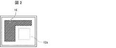
(絶縁シート)
図2には、図1の電子機器1のうち領域B部分の放熱部材14の、基板10側の面から見た平面図を示す。図2に示すように、放熱部材14の基板10側の面において、電子部品12に対向する領域以外の領域に絶縁シート16を備える。絶縁シート16により、基板の実装部品と放熱部材14との電気的導通を避けることができる。ただし、電子部品12に対向する領域においては、電子部品12と放熱部材14との間の断熱層13の厚みを充分に取るために絶縁シート16を設けない。絶縁シート16を設けず、電子部品12と放熱部材14との間の断熱層13の厚みを充分に取ることによって、放熱部材14および筐体30に電子部品12から発生した熱が伝わるのを抑制することができる。(Insulating sheet)
FIG. 2 shows a plan view of the
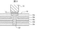
(基板10と放熱部材14との接続)
続いて、図3を参照して、基板10と放熱部材14との接続のされ方の一例について説明する。(Connection between the
Subsequently, an example of how the
図3は、図1における丸印A1で示した範囲の拡大断面図である。図2における丸印A2で示した範囲も同様の構成を有する。 FIG. 3 is an enlarged cross-sectional view of the range indicated by the circle A1 in FIG. The range indicated by the circle A2 in FIG. 2 has a similar configuration.
図3に示すように、基板10は、配線層10bとグラウンド層10dとを含む多層型基板であり、グラウンド層10dと放熱部材14とを接続する1又は複数のビア(特に放熱効果を向上させるビアをサーマルビアとも呼ぶ)10fを備えていてもよい。具体的には、基板10は、第1の樹脂層10a、配線層10b、第2の樹脂層10c、グラウンド層10d、及び第3の樹脂層10eが積層されて構成される。 As shown in FIG. 3, the
配線層10bは、基板10に実装される電子部品12や素子を互いに電気的に接続するための配線が配置されている層である。配線層10bは、例えば銅のような伝導性を有する材料によって構成される。また、図3に示すように、配線層10bは、第1の樹脂層10aと第2の樹脂層10cとの間に配置される。 The
グラウンド層10dは、基板10に実装される電子部品12や素子に接続されるグラウンド(接地)が配置されている層である。グラウンド層10dは、例えば銅のような伝導性を有する材料によって構成される。また、図3に示すように、グラウンド層10dは第2の樹脂層10cと第3の樹脂層10eとの間に配置される。但し、図3に示した構造は多層基板の構造の一例であって、樹脂層、配線層、グラウンド層の構造的順序や層数などは、図3に示した構造に限定されない。 The
ビア10fでは、基板10の裏面と表面とを接続するホールの内側に電気伝導度及び熱伝導度の高い材料、例えば銅等の金属が充填されている。ここで、ビア10fは、基板10の裏面から表面までを貫くスルーホール(スルーホールビア)であってもよい。スルーホールは、一例として銅のように電気伝導性及び熱伝導性を有する材料によって内側表面が覆われる構成であってもよい。 In the via 10f, the inside of the hole connecting the back surface and the front surface of the
図3に示すように、ビア10fは、グラウンド層10dに対して接触し、配線層10bの配線に接しないように配置されている。 As shown in FIG. 3, the via 10f is arranged so as to be in contact with the
また、基板10の表側の面における、ビア10fの端部は、放熱部材14に接触している。また、一例として、ビア10fの当該端部と放熱部材14とは半田15によって互いに固定される。 Further, the end portion of the via 10f on the front surface of the
上記構成によれば、電子部品12で発生した熱を基板10内に設けたグラウンド層10dに伝達させ、グラウンド層10dからビア10fを介して、放熱部材14に効率よく伝熱することができる。したがって、前述したように、基板10の電子部品12付近は配線もビア10fも多く設けられるため、基板10全体の熱伝導率より、電子部品12から放熱部材14までの熱伝導率は高くなる。なお、基板10におけるビア10fの数が多いほど、基板10全体の熱伝導率が向上し、放熱効果も高い。したがって、ビア10fの数をなるべく多くすることが好適である。 According to the above configuration, the heat generated by the
なお、基板10の電子部品12付近には、電気伝導率および熱伝導率の高い材料から構成される配線およびビア(サーマルビア)10fが多く設けられるため、基板10全体の熱伝導率より、電子部品12から放熱部材14までの領域の熱伝導率は高くなる。したがって、前述したように、放熱部材14の材料としては、基板10の電子部品12から放熱部材14までの熱伝導率以上の熱伝導率を有する材料で構成されることが好ましい。 Since many wirings and vias (thermal vias) 10f made of a material having high electric conductivity and thermal conductivity are provided in the vicinity of the
(電子部品の構成)
図4は、電子部品12の一例の断面図を示す。電子部品12は、少なくとも集積回路が形成されている集積回路層12aと、集積回路層12aよりも基板10から遠い側に、少なくともメモリが形成されているメモリ層12bと備えていてもよい。集積回路層12aとしては、例えば、SOC(System on Chip)であってもよい。集積回路層12aおよびメモリ層12bは、熱伝導率の低い樹脂層12cに囲まれている。したがって、上記構成では、集積回路層12aで発生した熱は、樹脂層12cおよびメモリ層12bに阻まれて、基板10と反対側からは放熱し難い。(Composition of electronic components)
FIG. 4 shows a cross-sectional view of an example of the
しかし、本実施形態の構成によれば、電子部品12から発生した熱を基板10側から好適に熱を除くことができる。したがって、上記のような電子部品であっても、電子機器での温度上昇を抑制することができる。 However, according to the configuration of the present embodiment, the heat generated from the
(電子機器の構成)
図5には、本発明の電子機器1の一例の側面断面図を示す。電子機器1は、基板10及び放熱部材14を少なくとも収容する筐体と、筐体のある一面側に配置された表示パネル50とを備え、表示パネル50とは反対側に配置されている筐体の部分から電子部品12の熱を放熱する。即ち、放熱部材14は、基板10から見て表示パネル50とは反対側に配置されてもよい。(Configuration of electronic devices)
FIG. 5 shows a side sectional view of an example of the electronic device 1 of the present invention. The electronic device 1 includes a housing that houses at least a
図5に示すように、本例に係る電子機器1は、筐体30を第1の筐体として備えており、更に、筐体40を第2の筐体として備えている。第2の筐体40の材料は、筐体30と同様の構成材料であってもよい。第1の筐体30および第2の筐体40の材料としては、金属、樹脂その他の材料が用いられてもよい。また、第2の筐体40には開口部か形成されており、当該開口部に表示パネル50が配置されている。 As shown in FIG. 5, the electronic device 1 according to this example includes a
なお、図5において、基板10から見て第2の筐体40側には部品を示していないが、これは本実施形態を限定するものではなく、本例に係る電子機器1は、基板10から見て第2の筐体40側に1又は複数の部品を備えていてもよい。 Note that, in FIG. 5, no component is shown on the
上記構成によれば、電子部品12で発生した熱は、放熱部材14を介して第1の筐体30(図5における右側)から広い範囲で放熱させることができる。したがって、通常ユーザの持ち手となる第1の筐体30から、ヒートスポットを発生させることなく、放熱させることができる。このように上記の例によれば、持ち手側の第1の筐体30にヒートスポットが生じることを抑制し、電子部品12から発生する熱を好適に放熱することができる。 According to the above configuration, the heat generated in the
〔まとめ〕
〔態様1〕
本発明の電子機器は、熱源となり得る電子部品と、当該電子部品が配置された基板とを備えた電子機器であって、前記基板において前記電子部品が配置された箇所を含む領域であって前記基板の表側又は裏側の領域を、断熱層を介して覆うと共に、前記基板に接続された放熱部材を備え、前記放熱部材は、前記基板の熱伝導率以上の熱伝導率を有する材料から構成されている。〔summary〕
[Aspect 1]
The electronic device of the present invention is an electronic device including an electronic component that can be a heat source and a substrate on which the electronic component is arranged, and is a region including a portion of the substrate on which the electronic component is arranged. The area on the front side or the back side of the substrate is covered with a heat insulating layer, and a heat radiating member connected to the substrate is provided. ing.
〔態様2〕
本発明の電子機器において、前記放熱部材は熱伝導率が50W/mK以上である材料から構成されていてもよい。[Aspect 2]
In the electronic device of the present invention, the heat radiating member may be made of a material having a thermal conductivity of 50 W / mK or more.
前記構成によれば、電子部品で発生した熱が、効率よく放熱部材に伝わり、局所的に温度上昇が生じるのを防ぐことができる。更に、電子部品と放熱部材の間に、断熱層を設けることにより、電子部品で発生した熱が局所的に放熱部材に伝わることを抑制することができる。したがって、電子機器内で、ヒートスポットが発生するのを防ぐことができる。 According to the above configuration, the heat generated in the electronic component is efficiently transferred to the heat radiating member, and it is possible to prevent the temperature from rising locally. Further, by providing a heat insulating layer between the electronic component and the heat radiating member, it is possible to suppress the heat generated by the electronic component from being locally transferred to the heat radiating member. Therefore, it is possible to prevent heat spots from occurring in the electronic device.
〔態様3〕
本発明の電子機器において、前記放熱部材の材料は銅を含んでもよい。[Aspect 3]
In the electronic device of the present invention, the material of the heat radiating member may contain copper.
前記構成によれば、電気伝導度、及び熱伝導性が共に高く、安価な銅を放熱部材として用いることにより、電子機器の温度上昇を抑制することができる。 According to the above configuration, the temperature rise of the electronic device can be suppressed by using inexpensive copper having high electrical conductivity and thermal conductivity as the heat radiating member.
〔態様4〕
本発明の電子機器において、前記断熱層は、空気層および断熱部材の少なくとも何れかを含んでいてもよい。[Aspect 4]
In the electronic device of the present invention, the heat insulating layer may include at least one of an air layer and a heat insulating member.
前記構成によれば、電子部品と放熱部材の間に何も設置せず空気層とする、または、熱伝導率の低い断熱部材を設置することによって、電子部品から放熱部材に局所的に熱が伝わるのを抑制し、電子機器におけるヒートスポットの発生を防止することができる。 According to the above configuration, heat is locally generated from the electronic component to the heat radiating member by forming an air layer without installing anything between the electronic component and the heat radiating member, or by installing a heat insulating member having low thermal conductivity. It is possible to suppress transmission and prevent the generation of heat spots in electronic devices.
〔態様5〕
本発明の電子機器において、前記放熱部材の前記基板側の面において、前記電子部品に対向する領域以外の領域に絶縁シートを備えてもよい。[Aspect 5]
In the electronic device of the present invention, an insulating sheet may be provided on the surface of the heat radiating member on the substrate side in a region other than the region facing the electronic component.
前記構成によれば、絶縁シートによって基板に配置された実装部品と放熱部材の間の電気的導通を防ぐことができるとともに、発熱性の電子部品と放熱部材の間には絶縁シートを設けないことによって、電子部品と放熱部材の間に充分な厚さの断熱層を設けることができる。 According to the above configuration, the insulating sheet can prevent electrical conduction between the mounting component and the heat radiating member arranged on the substrate, and the insulating sheet is not provided between the heat generating electronic component and the heat radiating member. Therefore, a heat insulating layer having a sufficient thickness can be provided between the electronic component and the heat radiating member.
〔態様6〕
本発明の電子機器において、前記基板は、配線層とグラウンド層とを含む多層型基板であり、前記グラウンド層と前記放熱部材とを接続する1又は複数のビアを備えていてもよい。[Aspect 6]
In the electronic device of the present invention, the substrate is a multilayer substrate including a wiring layer and a ground layer, and may include one or a plurality of vias connecting the ground layer and the heat radiating member.
前記構成によれば、電子部品に発生した熱を、ビアから放熱部材に効率的に伝達することができる。 According to the above configuration, the heat generated in the electronic component can be efficiently transferred from the via to the heat radiating member.
〔態様7〕
本発明の電子機器において、前記電子部品は、少なくとも集積回路が形成されている集積回路層と、前記集積回路層よりも前記基板から遠い側に、少なくともメモリが形成されているメモリ層と備えていてもよい。[Aspect 7]
In the electronic device of the present invention, the electronic component includes at least an integrated circuit layer in which an integrated circuit is formed, and a memory layer in which at least a memory is formed on a side farther from the substrate than the integrated circuit layer. You may.
前記構成によれば、放熱にとって妨げとなるものが存在しない基板側から、電子部品に発生した熱を効率よく発散させることができる。 According to the above configuration, the heat generated in the electronic component can be efficiently dissipated from the substrate side where there is no obstacle to heat dissipation.
〔態様8〕
本発明の電子機器において、前記基板及び前記放熱部材を少なくとも収容する筐体と、前記筐体のある一面側に配置された表示パネルとを備え、前記表示パネルとは反対側に配置されている筐体の部分から前記電子部品の熱を放熱してもよい。[Aspect 8]
The electronic device of the present invention includes a housing that houses at least the substrate and the heat radiating member, and a display panel arranged on one side of the housing, and is arranged on the opposite side of the display panel. The heat of the electronic component may be dissipated from the housing portion.
前記構成によれば、通常ユーザが電子機器を持つ側、即ち、表示パネルとは反対側から広い範囲に亘って熱を発散させることができる。したがって、ユーザの持ち手が熱くなる等の問題を防ぐことができる。 According to the above configuration, heat can be dissipated over a wide range from the side where the user usually holds the electronic device, that is, the side opposite to the display panel. Therefore, it is possible to prevent problems such as the user's handle becoming hot.
本発明は上述した各実施形態に限定されるものではなく、請求項に示した範囲で種々の変更が可能であり、異なる実施形態にそれぞれ開示された技術的手段を適宜組み合わせて得られる実施形態についても本発明の技術的範囲に含まれる。さらに、各実施形態にそれぞれ開示された技術的手段を組み合わせることにより、新しい技術的特徴を形成することができる。 The present invention is not limited to the above-described embodiments, and various modifications can be made within the scope of the claims, and the embodiments obtained by appropriately combining the technical means disclosed in the different embodiments. Is also included in the technical scope of the present invention. Furthermore, new technical features can be formed by combining the technical means disclosed in each embodiment.
1 電子機器
10 基板
10b 配線層
10a 第1の樹脂層
10c 第2の樹脂層
10d グラウンド層
10e 第3の樹脂層
10f ビア
12 電子部品
12a 集積回路層
12b メモリ層
12c 樹脂層
13 断熱層
14 放熱部材
15 半田
16 絶縁シート
30 第1の筐体
40 第2の筐体
50 表示パネル1
Claims (8)
Translated fromJapanese前記基板において前記電子部品が配置された箇所を含む領域であって前記基板の表側又は裏側の領域を、断熱層を介して覆うと共に、前記基板に接続された放熱部材を備え、
前記放熱部材は、前記基板の熱伝導率以上の熱伝導率を有する材料から構成されている、
電子機器。An electronic device including an electronic component that can be a heat source and a substrate on which the electronic component is arranged.
A region including a portion of the substrate on which the electronic components are arranged, the front side or the back side region of the substrate is covered with a heat insulating layer, and a heat radiating member connected to the substrate is provided.
The heat radiating member is made of a material having a thermal conductivity equal to or higher than the thermal conductivity of the substrate.
Electronics.
請求項1に記載の電子機器。The heat radiating member is made of a material having a thermal conductivity of 50 W / mK or more.
The electronic device according to claim 1.
請求項1又は2に記載の電子機器。The electronic device according to claim 1 or 2, wherein the material of the heat radiating member contains copper.
請求項1から3の何れか1項に記載の電子機器。The electronic device according to any one of claims 1 to 3, wherein the heat insulating layer includes at least one of an air layer and a heat insulating member.
請求項1から4の何れか1項に電子機器。The electronic device according to any one of claims 1 to 4, wherein an insulating sheet is provided in a region other than the region facing the electronic component on the surface of the heat radiating member on the substrate side.
配線層とグラウンド層とを含む多層型基板であり、
前記グラウンド層と前記放熱部材とを接続する1又は複数のビアを備えている
請求項1から5の何れか1項に記載の電子機器。The substrate is
It is a multi-layer board including a wiring layer and a ground layer.
The electronic device according to any one of claims 1 to 5, further comprising one or a plurality of vias connecting the ground layer and the heat radiating member.
少なくとも集積回路が形成されている集積回路層と、
前記集積回路層よりも前記基板から遠い側に、少なくともメモリが形成されているメモリ層と備えている
請求項1から6の何れか1項に記載の電子機器。The electronic component is
At least the integrated circuit layer on which the integrated circuit is formed,
The electronic device according to any one of claims 1 to 6, further comprising a memory layer in which at least a memory is formed on a side farther from the substrate than the integrated circuit layer.
前記筐体のある一面側に配置された表示パネルと、を備え、
前記表示パネルとは反対側に配置されている筐体の部分から前記電子部品の熱を放熱する
ことを特徴とする請求項1から7の何れか1項に記載の電子機器。A housing that houses at least the substrate and the heat radiating member,
A display panel arranged on one side of the housing is provided.
The electronic device according to any one of claims 1 to 7, wherein heat of the electronic component is dissipated from a portion of a housing arranged on the side opposite to the display panel.
Priority Applications (3)
| Application Number | Priority Date | Filing Date | Title |
|---|---|---|---|
| JP2020023827AJP2021129059A (en) | 2020-02-14 | 2020-02-14 | Electronic apparatus |
| CN202110185172.0ACN113268127A (en) | 2020-02-14 | 2021-02-10 | Electronic device |
| US17/174,648US20210259136A1 (en) | 2020-02-14 | 2021-02-12 | Electronic device |
Applications Claiming Priority (1)
| Application Number | Priority Date | Filing Date | Title |
|---|---|---|---|
| JP2020023827AJP2021129059A (en) | 2020-02-14 | 2020-02-14 | Electronic apparatus |
Publications (1)
| Publication Number | Publication Date |
|---|---|
| JP2021129059Atrue JP2021129059A (en) | 2021-09-02 |
Family
ID=77228182
Family Applications (1)
| Application Number | Title | Priority Date | Filing Date |
|---|---|---|---|
| JP2020023827APendingJP2021129059A (en) | 2020-02-14 | 2020-02-14 | Electronic apparatus |
Country Status (3)
| Country | Link |
|---|---|
| US (1) | US20210259136A1 (en) |
| JP (1) | JP2021129059A (en) |
| CN (1) | CN113268127A (en) |
Families Citing this family (2)
| Publication number | Priority date | Publication date | Assignee | Title |
|---|---|---|---|---|
| CN114356058B (en)* | 2021-12-31 | 2024-11-08 | 北京有竹居网络技术有限公司 | Internal cavity structure of electronic equipment |
| TWI799339B (en)* | 2022-08-22 | 2023-04-11 | 華碩電腦股份有限公司 | Handheld electronic device |
Citations (12)
| Publication number | Priority date | Publication date | Assignee | Title |
|---|---|---|---|---|
| JP2000277976A (en)* | 1999-03-24 | 2000-10-06 | Matsushita Electric Ind Co Ltd | Heat dissipation device for electric circuit |
| JP2006210940A (en)* | 2006-03-23 | 2006-08-10 | Mitsubishi Electric Corp | Communication equipment |
| JP2008277432A (en)* | 2007-04-26 | 2008-11-13 | Kaneka Corp | Heat dissipation structure |
| JP2010103375A (en)* | 2008-10-24 | 2010-05-06 | Nec Saitama Ltd | Mounting structure for shield cover, shield cover, and shield frame |
| JP2012160651A (en)* | 2011-02-02 | 2012-08-23 | Mitsubishi Electric Corp | Electronic apparatus |
| JP2013097224A (en)* | 2011-11-02 | 2013-05-20 | Sharp Corp | Portable communication terminal |
| JP2014060285A (en)* | 2012-09-18 | 2014-04-03 | Fujitsu Ltd | Electronic apparatus |
| JP2014106917A (en)* | 2012-11-29 | 2014-06-09 | Canon Inc | Information processing unit, control method thereof and program |
| WO2015137257A1 (en)* | 2014-03-14 | 2015-09-17 | 株式会社カネカ | Electronic terminal device and method for assembling same |
| WO2016031807A1 (en)* | 2014-08-26 | 2016-03-03 | 三菱電機株式会社 | High-frequency module |
| JP2016114646A (en)* | 2014-12-11 | 2016-06-23 | 日本精機株式会社 | Display device |
| JP2018014485A (en)* | 2016-05-31 | 2018-01-25 | Jx金属株式会社 | Structure with metal material for heat dissipation, printed circuit board, electronic equipment and metal material for heat dissipation |
Family Cites Families (5)
| Publication number | Priority date | Publication date | Assignee | Title |
|---|---|---|---|---|
| WO2001095687A1 (en)* | 2000-06-06 | 2001-12-13 | Mitsubishi Denki Kabushiki Kaisha | Cooling structure of communication device |
| US20030112603A1 (en)* | 2001-12-13 | 2003-06-19 | Roesner Arlen L. | Thermal interface |
| JP5665948B1 (en)* | 2013-11-14 | 2015-02-04 | 株式会社フジクラ | Cooling structure for portable electronic devices |
| CN203884130U (en)* | 2014-06-17 | 2014-10-15 | 奇鋐科技股份有限公司 | Electronic substrate heat radiation structure |
| JP6665864B2 (en)* | 2015-11-17 | 2020-03-13 | 株式会社村田製作所 | Multilayer substrate and electronic equipment |
- 2020
- 2020-02-14JPJP2020023827Apatent/JP2021129059A/enactivePending
- 2021
- 2021-02-10CNCN202110185172.0Apatent/CN113268127A/enactivePending
- 2021-02-12USUS17/174,648patent/US20210259136A1/ennot_activeAbandoned
Patent Citations (12)
| Publication number | Priority date | Publication date | Assignee | Title |
|---|---|---|---|---|
| JP2000277976A (en)* | 1999-03-24 | 2000-10-06 | Matsushita Electric Ind Co Ltd | Heat dissipation device for electric circuit |
| JP2006210940A (en)* | 2006-03-23 | 2006-08-10 | Mitsubishi Electric Corp | Communication equipment |
| JP2008277432A (en)* | 2007-04-26 | 2008-11-13 | Kaneka Corp | Heat dissipation structure |
| JP2010103375A (en)* | 2008-10-24 | 2010-05-06 | Nec Saitama Ltd | Mounting structure for shield cover, shield cover, and shield frame |
| JP2012160651A (en)* | 2011-02-02 | 2012-08-23 | Mitsubishi Electric Corp | Electronic apparatus |
| JP2013097224A (en)* | 2011-11-02 | 2013-05-20 | Sharp Corp | Portable communication terminal |
| JP2014060285A (en)* | 2012-09-18 | 2014-04-03 | Fujitsu Ltd | Electronic apparatus |
| JP2014106917A (en)* | 2012-11-29 | 2014-06-09 | Canon Inc | Information processing unit, control method thereof and program |
| WO2015137257A1 (en)* | 2014-03-14 | 2015-09-17 | 株式会社カネカ | Electronic terminal device and method for assembling same |
| WO2016031807A1 (en)* | 2014-08-26 | 2016-03-03 | 三菱電機株式会社 | High-frequency module |
| JP2016114646A (en)* | 2014-12-11 | 2016-06-23 | 日本精機株式会社 | Display device |
| JP2018014485A (en)* | 2016-05-31 | 2018-01-25 | Jx金属株式会社 | Structure with metal material for heat dissipation, printed circuit board, electronic equipment and metal material for heat dissipation |
Also Published As
| Publication number | Publication date |
|---|---|
| CN113268127A (en) | 2021-08-17 |
| US20210259136A1 (en) | 2021-08-19 |
Similar Documents
| Publication | Publication Date | Title |
|---|---|---|
| EP3107361B1 (en) | Heat dissipation assembly and electronic device | |
| CN100505781C (en) | Mobile terminal device and method for radiating heat therefrom | |
| JP6707960B2 (en) | Electronics | |
| US7623349B2 (en) | Thermal management apparatus and method for a circuit substrate | |
| JP2008140924A (en) | Electronics | |
| EP3104407B1 (en) | Mobile terminal | |
| KR102674888B1 (en) | Printed circuit board assembly | |
| JP2012238794A (en) | Electronic apparatus and power conversion apparatus provided with the same | |
| JPH10260230A (en) | Apparatus for cooling heat-generating body | |
| WO2017022221A1 (en) | Heat dissipating structure and electronic apparatus | |
| JP2021129059A (en) | Electronic apparatus | |
| JP2008218618A (en) | Printed wiring board | |
| TW201902310A (en) | Circuit board having a heat conducting and heat dissipating function including a first heat insulating and dissipating material coated on the board body | |
| TW200423345A (en) | Thermal-conductive substrate package | |
| JP6311222B2 (en) | Electronic device and heat dissipation method | |
| US20210259137A1 (en) | Electronic device | |
| KR102444136B1 (en) | Millimeter wave transceiver with improved heat dissipation | |
| JP2007174526A (en) | Heat dissipation structure for portable electronic devices | |
| JP5533787B2 (en) | Heat dissipation device | |
| US8363398B2 (en) | Electronic device with heat dissipation casing | |
| CN105050369B (en) | A kind of intelligent terminal | |
| JP2007049015A (en) | Electronic device structure and electronic device using the same | |
| JP2007115097A (en) | Electronic equipment and board unit | |
| JP2006054318A (en) | Electric component module and its manufacturing method | |
| JP2008091567A (en) | Heat sink and heat sink mounting structure |
Legal Events
| Date | Code | Title | Description |
|---|---|---|---|
| A621 | Written request for application examination | Free format text:JAPANESE INTERMEDIATE CODE: A621 Effective date:20220921 | |
| A977 | Report on retrieval | Free format text:JAPANESE INTERMEDIATE CODE: A971007 Effective date:20230621 | |
| A131 | Notification of reasons for refusal | Free format text:JAPANESE INTERMEDIATE CODE: A131 Effective date:20230627 | |
| A02 | Decision of refusal | Free format text:JAPANESE INTERMEDIATE CODE: A02 Effective date:20231219 |