JP2021119635A - Semiconductor device - Google Patents
Semiconductor deviceDownload PDFInfo
- Publication number
- JP2021119635A JP2021119635AJP2021078512AJP2021078512AJP2021119635AJP 2021119635 AJP2021119635 AJP 2021119635AJP 2021078512 AJP2021078512 AJP 2021078512AJP 2021078512 AJP2021078512 AJP 2021078512AJP 2021119635 AJP2021119635 AJP 2021119635A
- Authority
- JP
- Japan
- Prior art keywords
- film
- oxide semiconductor
- wiring
- insulating film
- transistor
- Prior art date
- Legal status (The legal status is an assumption and is not a legal conclusion. Google has not performed a legal analysis and makes no representation as to the accuracy of the status listed.)
- Withdrawn
Links
Images


Classifications
- H—ELECTRICITY
- H10—SEMICONDUCTOR DEVICES; ELECTRIC SOLID-STATE DEVICES NOT OTHERWISE PROVIDED FOR
- H10D—INORGANIC ELECTRIC SEMICONDUCTOR DEVICES
- H10D86/00—Integrated devices formed in or on insulating or conducting substrates, e.g. formed in silicon-on-insulator [SOI] substrates or on stainless steel or glass substrates
- H10D86/40—Integrated devices formed in or on insulating or conducting substrates, e.g. formed in silicon-on-insulator [SOI] substrates or on stainless steel or glass substrates characterised by multiple TFTs
- H10D86/60—Integrated devices formed in or on insulating or conducting substrates, e.g. formed in silicon-on-insulator [SOI] substrates or on stainless steel or glass substrates characterised by multiple TFTs wherein the TFTs are in active matrices
- G—PHYSICS
- G06—COMPUTING OR CALCULATING; COUNTING
- G06F—ELECTRIC DIGITAL DATA PROCESSING
- G06F3/00—Input arrangements for transferring data to be processed into a form capable of being handled by the computer; Output arrangements for transferring data from processing unit to output unit, e.g. interface arrangements
- G06F3/01—Input arrangements or combined input and output arrangements for interaction between user and computer
- G06F3/03—Arrangements for converting the position or the displacement of a member into a coded form
- G06F3/041—Digitisers, e.g. for touch screens or touch pads, characterised by the transducing means
- H—ELECTRICITY
- H10—SEMICONDUCTOR DEVICES; ELECTRIC SOLID-STATE DEVICES NOT OTHERWISE PROVIDED FOR
- H10D—INORGANIC ELECTRIC SEMICONDUCTOR DEVICES
- H10D30/00—Field-effect transistors [FET]
- H10D30/60—Insulated-gate field-effect transistors [IGFET]
- H10D30/67—Thin-film transistors [TFT]
- H10D30/6729—Thin-film transistors [TFT] characterised by the electrodes
- H10D30/673—Thin-film transistors [TFT] characterised by the electrodes characterised by the shapes, relative sizes or dispositions of the gate electrodes
- H—ELECTRICITY
- H10—SEMICONDUCTOR DEVICES; ELECTRIC SOLID-STATE DEVICES NOT OTHERWISE PROVIDED FOR
- H10D—INORGANIC ELECTRIC SEMICONDUCTOR DEVICES
- H10D30/00—Field-effect transistors [FET]
- H10D30/60—Insulated-gate field-effect transistors [IGFET]
- H10D30/67—Thin-film transistors [TFT]
- H10D30/6729—Thin-film transistors [TFT] characterised by the electrodes
- H10D30/6737—Thin-film transistors [TFT] characterised by the electrodes characterised by the electrode materials
- H10D30/6739—Conductor-insulator-semiconductor electrodes
- H—ELECTRICITY
- H10—SEMICONDUCTOR DEVICES; ELECTRIC SOLID-STATE DEVICES NOT OTHERWISE PROVIDED FOR
- H10D—INORGANIC ELECTRIC SEMICONDUCTOR DEVICES
- H10D30/00—Field-effect transistors [FET]
- H10D30/60—Insulated-gate field-effect transistors [IGFET]
- H10D30/67—Thin-film transistors [TFT]
- H10D30/674—Thin-film transistors [TFT] characterised by the active materials
- H10D30/6755—Oxide semiconductors, e.g. zinc oxide, copper aluminium oxide or cadmium stannate
- H—ELECTRICITY
- H10—SEMICONDUCTOR DEVICES; ELECTRIC SOLID-STATE DEVICES NOT OTHERWISE PROVIDED FOR
- H10D—INORGANIC ELECTRIC SEMICONDUCTOR DEVICES
- H10D86/00—Integrated devices formed in or on insulating or conducting substrates, e.g. formed in silicon-on-insulator [SOI] substrates or on stainless steel or glass substrates
- H10D86/01—Manufacture or treatment
- H10D86/021—Manufacture or treatment of multiple TFTs
- H10D86/0231—Manufacture or treatment of multiple TFTs using masks, e.g. half-tone masks
- H—ELECTRICITY
- H10—SEMICONDUCTOR DEVICES; ELECTRIC SOLID-STATE DEVICES NOT OTHERWISE PROVIDED FOR
- H10D—INORGANIC ELECTRIC SEMICONDUCTOR DEVICES
- H10D86/00—Integrated devices formed in or on insulating or conducting substrates, e.g. formed in silicon-on-insulator [SOI] substrates or on stainless steel or glass substrates
- H10D86/40—Integrated devices formed in or on insulating or conducting substrates, e.g. formed in silicon-on-insulator [SOI] substrates or on stainless steel or glass substrates characterised by multiple TFTs
- H10D86/421—Integrated devices formed in or on insulating or conducting substrates, e.g. formed in silicon-on-insulator [SOI] substrates or on stainless steel or glass substrates characterised by multiple TFTs having a particular composition, shape or crystalline structure of the active layer
- H10D86/423—Integrated devices formed in or on insulating or conducting substrates, e.g. formed in silicon-on-insulator [SOI] substrates or on stainless steel or glass substrates characterised by multiple TFTs having a particular composition, shape or crystalline structure of the active layer comprising semiconductor materials not belonging to the Group IV, e.g. InGaZnO
- H—ELECTRICITY
- H10—SEMICONDUCTOR DEVICES; ELECTRIC SOLID-STATE DEVICES NOT OTHERWISE PROVIDED FOR
- H10D—INORGANIC ELECTRIC SEMICONDUCTOR DEVICES
- H10D86/00—Integrated devices formed in or on insulating or conducting substrates, e.g. formed in silicon-on-insulator [SOI] substrates or on stainless steel or glass substrates
- H10D86/40—Integrated devices formed in or on insulating or conducting substrates, e.g. formed in silicon-on-insulator [SOI] substrates or on stainless steel or glass substrates characterised by multiple TFTs
- H10D86/441—Interconnections, e.g. scanning lines
- H—ELECTRICITY
- H10—SEMICONDUCTOR DEVICES; ELECTRIC SOLID-STATE DEVICES NOT OTHERWISE PROVIDED FOR
- H10D—INORGANIC ELECTRIC SEMICONDUCTOR DEVICES
- H10D86/00—Integrated devices formed in or on insulating or conducting substrates, e.g. formed in silicon-on-insulator [SOI] substrates or on stainless steel or glass substrates
- H10D86/40—Integrated devices formed in or on insulating or conducting substrates, e.g. formed in silicon-on-insulator [SOI] substrates or on stainless steel or glass substrates characterised by multiple TFTs
- H10D86/451—Integrated devices formed in or on insulating or conducting substrates, e.g. formed in silicon-on-insulator [SOI] substrates or on stainless steel or glass substrates characterised by multiple TFTs characterised by the compositions or shapes of the interlayer dielectrics
- G—PHYSICS
- G02—OPTICS
- G02F—OPTICAL DEVICES OR ARRANGEMENTS FOR THE CONTROL OF LIGHT BY MODIFICATION OF THE OPTICAL PROPERTIES OF THE MEDIA OF THE ELEMENTS INVOLVED THEREIN; NON-LINEAR OPTICS; FREQUENCY-CHANGING OF LIGHT; OPTICAL LOGIC ELEMENTS; OPTICAL ANALOGUE/DIGITAL CONVERTERS
- G02F1/00—Devices or arrangements for the control of the intensity, colour, phase, polarisation or direction of light arriving from an independent light source, e.g. switching, gating or modulating; Non-linear optics
- G02F1/01—Devices or arrangements for the control of the intensity, colour, phase, polarisation or direction of light arriving from an independent light source, e.g. switching, gating or modulating; Non-linear optics for the control of the intensity, phase, polarisation or colour
- G02F1/13—Devices or arrangements for the control of the intensity, colour, phase, polarisation or direction of light arriving from an independent light source, e.g. switching, gating or modulating; Non-linear optics for the control of the intensity, phase, polarisation or colour based on liquid crystals, e.g. single liquid crystal display cells
- G02F1/133—Constructional arrangements; Operation of liquid crystal cells; Circuit arrangements
- G02F1/13306—Circuit arrangements or driving methods for the control of single liquid crystal cells
- G—PHYSICS
- G02—OPTICS
- G02F—OPTICAL DEVICES OR ARRANGEMENTS FOR THE CONTROL OF LIGHT BY MODIFICATION OF THE OPTICAL PROPERTIES OF THE MEDIA OF THE ELEMENTS INVOLVED THEREIN; NON-LINEAR OPTICS; FREQUENCY-CHANGING OF LIGHT; OPTICAL LOGIC ELEMENTS; OPTICAL ANALOGUE/DIGITAL CONVERTERS
- G02F1/00—Devices or arrangements for the control of the intensity, colour, phase, polarisation or direction of light arriving from an independent light source, e.g. switching, gating or modulating; Non-linear optics
- G02F1/01—Devices or arrangements for the control of the intensity, colour, phase, polarisation or direction of light arriving from an independent light source, e.g. switching, gating or modulating; Non-linear optics for the control of the intensity, phase, polarisation or colour
- G02F1/13—Devices or arrangements for the control of the intensity, colour, phase, polarisation or direction of light arriving from an independent light source, e.g. switching, gating or modulating; Non-linear optics for the control of the intensity, phase, polarisation or colour based on liquid crystals, e.g. single liquid crystal display cells
- G02F1/133—Constructional arrangements; Operation of liquid crystal cells; Circuit arrangements
- G02F1/1333—Constructional arrangements; Manufacturing methods
- G02F1/133345—Insulating layers
- G—PHYSICS
- G02—OPTICS
- G02F—OPTICAL DEVICES OR ARRANGEMENTS FOR THE CONTROL OF LIGHT BY MODIFICATION OF THE OPTICAL PROPERTIES OF THE MEDIA OF THE ELEMENTS INVOLVED THEREIN; NON-LINEAR OPTICS; FREQUENCY-CHANGING OF LIGHT; OPTICAL LOGIC ELEMENTS; OPTICAL ANALOGUE/DIGITAL CONVERTERS
- G02F1/00—Devices or arrangements for the control of the intensity, colour, phase, polarisation or direction of light arriving from an independent light source, e.g. switching, gating or modulating; Non-linear optics
- G02F1/01—Devices or arrangements for the control of the intensity, colour, phase, polarisation or direction of light arriving from an independent light source, e.g. switching, gating or modulating; Non-linear optics for the control of the intensity, phase, polarisation or colour
- G02F1/13—Devices or arrangements for the control of the intensity, colour, phase, polarisation or direction of light arriving from an independent light source, e.g. switching, gating or modulating; Non-linear optics for the control of the intensity, phase, polarisation or colour based on liquid crystals, e.g. single liquid crystal display cells
- G02F1/133—Constructional arrangements; Operation of liquid crystal cells; Circuit arrangements
- G02F1/1333—Constructional arrangements; Manufacturing methods
- G02F1/13338—Input devices, e.g. touch panels
- G—PHYSICS
- G02—OPTICS
- G02F—OPTICAL DEVICES OR ARRANGEMENTS FOR THE CONTROL OF LIGHT BY MODIFICATION OF THE OPTICAL PROPERTIES OF THE MEDIA OF THE ELEMENTS INVOLVED THEREIN; NON-LINEAR OPTICS; FREQUENCY-CHANGING OF LIGHT; OPTICAL LOGIC ELEMENTS; OPTICAL ANALOGUE/DIGITAL CONVERTERS
- G02F1/00—Devices or arrangements for the control of the intensity, colour, phase, polarisation or direction of light arriving from an independent light source, e.g. switching, gating or modulating; Non-linear optics
- G02F1/01—Devices or arrangements for the control of the intensity, colour, phase, polarisation or direction of light arriving from an independent light source, e.g. switching, gating or modulating; Non-linear optics for the control of the intensity, phase, polarisation or colour
- G02F1/13—Devices or arrangements for the control of the intensity, colour, phase, polarisation or direction of light arriving from an independent light source, e.g. switching, gating or modulating; Non-linear optics for the control of the intensity, phase, polarisation or colour based on liquid crystals, e.g. single liquid crystal display cells
- G02F1/133—Constructional arrangements; Operation of liquid crystal cells; Circuit arrangements
- G02F1/1333—Constructional arrangements; Manufacturing methods
- G02F1/1343—Electrodes
- G02F1/134309—Electrodes characterised by their geometrical arrangement
- G02F1/134336—Matrix
- G—PHYSICS
- G02—OPTICS
- G02F—OPTICAL DEVICES OR ARRANGEMENTS FOR THE CONTROL OF LIGHT BY MODIFICATION OF THE OPTICAL PROPERTIES OF THE MEDIA OF THE ELEMENTS INVOLVED THEREIN; NON-LINEAR OPTICS; FREQUENCY-CHANGING OF LIGHT; OPTICAL LOGIC ELEMENTS; OPTICAL ANALOGUE/DIGITAL CONVERTERS
- G02F1/00—Devices or arrangements for the control of the intensity, colour, phase, polarisation or direction of light arriving from an independent light source, e.g. switching, gating or modulating; Non-linear optics
- G02F1/01—Devices or arrangements for the control of the intensity, colour, phase, polarisation or direction of light arriving from an independent light source, e.g. switching, gating or modulating; Non-linear optics for the control of the intensity, phase, polarisation or colour
- G02F1/13—Devices or arrangements for the control of the intensity, colour, phase, polarisation or direction of light arriving from an independent light source, e.g. switching, gating or modulating; Non-linear optics for the control of the intensity, phase, polarisation or colour based on liquid crystals, e.g. single liquid crystal display cells
- G02F1/133—Constructional arrangements; Operation of liquid crystal cells; Circuit arrangements
- G02F1/136—Liquid crystal cells structurally associated with a semi-conducting layer or substrate, e.g. cells forming part of an integrated circuit
- G02F1/1362—Active matrix addressed cells
- G02F1/136286—Wiring, e.g. gate line, drain line
- G—PHYSICS
- G02—OPTICS
- G02F—OPTICAL DEVICES OR ARRANGEMENTS FOR THE CONTROL OF LIGHT BY MODIFICATION OF THE OPTICAL PROPERTIES OF THE MEDIA OF THE ELEMENTS INVOLVED THEREIN; NON-LINEAR OPTICS; FREQUENCY-CHANGING OF LIGHT; OPTICAL LOGIC ELEMENTS; OPTICAL ANALOGUE/DIGITAL CONVERTERS
- G02F1/00—Devices or arrangements for the control of the intensity, colour, phase, polarisation or direction of light arriving from an independent light source, e.g. switching, gating or modulating; Non-linear optics
- G02F1/01—Devices or arrangements for the control of the intensity, colour, phase, polarisation or direction of light arriving from an independent light source, e.g. switching, gating or modulating; Non-linear optics for the control of the intensity, phase, polarisation or colour
- G02F1/13—Devices or arrangements for the control of the intensity, colour, phase, polarisation or direction of light arriving from an independent light source, e.g. switching, gating or modulating; Non-linear optics for the control of the intensity, phase, polarisation or colour based on liquid crystals, e.g. single liquid crystal display cells
- G02F1/133—Constructional arrangements; Operation of liquid crystal cells; Circuit arrangements
- G02F1/136—Liquid crystal cells structurally associated with a semi-conducting layer or substrate, e.g. cells forming part of an integrated circuit
- G02F1/1362—Active matrix addressed cells
- G02F1/1368—Active matrix addressed cells in which the switching element is a three-electrode device
- G—PHYSICS
- G02—OPTICS
- G02F—OPTICAL DEVICES OR ARRANGEMENTS FOR THE CONTROL OF LIGHT BY MODIFICATION OF THE OPTICAL PROPERTIES OF THE MEDIA OF THE ELEMENTS INVOLVED THEREIN; NON-LINEAR OPTICS; FREQUENCY-CHANGING OF LIGHT; OPTICAL LOGIC ELEMENTS; OPTICAL ANALOGUE/DIGITAL CONVERTERS
- G02F2201/00—Constructional arrangements not provided for in groups G02F1/00 - G02F7/00
- G02F2201/12—Constructional arrangements not provided for in groups G02F1/00 - G02F7/00 electrode
- G02F2201/123—Constructional arrangements not provided for in groups G02F1/00 - G02F7/00 electrode pixel
- G—PHYSICS
- G06—COMPUTING OR CALCULATING; COUNTING
- G06F—ELECTRIC DIGITAL DATA PROCESSING
- G06F2203/00—Indexing scheme relating to G06F3/00 - G06F3/048
- G06F2203/041—Indexing scheme relating to G06F3/041 - G06F3/045
- G06F2203/04103—Manufacturing, i.e. details related to manufacturing processes specially suited for touch sensitive devices
Landscapes
- Engineering & Computer Science (AREA)
- General Engineering & Computer Science (AREA)
- Theoretical Computer Science (AREA)
- Human Computer Interaction (AREA)
- Physics & Mathematics (AREA)
- General Physics & Mathematics (AREA)
- Thin Film Transistor (AREA)
- Internal Circuitry In Semiconductor Integrated Circuit Devices (AREA)
- Liquid Crystal (AREA)
- Semiconductor Integrated Circuits (AREA)
Abstract
Description
Translated fromJapanese 酸化物半導体膜を用いたトランジスタを有する半導体装置に関する。また該半導体装置
を用いた表示装置に関する。The present invention relates to a semiconductor device having a transistor using an oxide semiconductor film. The present invention also relates to a display device using the semiconductor device.
基板上に形成された半導体薄膜を用いてトランジスタ(薄膜トランジスタ(TFT)と
もいう。)を構成する技術が注目されている。該トランジスタは、集積回路(IC)や画
像表示装置(表示装置)のような電子デバイスに広く応用されている。トランジスタに適
用可能な半導体薄膜としてシリコン系半導体材料が広く知られているが、その他の材料と
して酸化物半導体が注目されている。Attention is being paid to a technique for forming a transistor (also referred to as a thin film transistor (TFT)) using a semiconductor thin film formed on a substrate. The transistor is widely applied to electronic devices such as integrated circuits (ICs) and image display devices (display devices). Silicon-based semiconductor materials are widely known as semiconductor thin films applicable to transistors, but oxide semiconductors are attracting attention as other materials.
例えば、トランジスタの活性層として、インジウム(In)、ガリウム(Ga)及び亜
鉛(Zn)を含む酸化物半導体を用いたトランジスタが開示されている(特許文献1及び
特許文献2参照)。For example, a transistor using an oxide semiconductor containing indium (In), gallium (Ga) and zinc (Zn) as an active layer of the transistor is disclosed (see
また、近年では電子機器の高性能化、小型化、または軽量化に伴い、微細化されたトラ
ンジスタまたは接続配線等を高密度に集積して駆動回路を形成し、該駆動回路と表示装置
を同一基板上に設ける駆動回路一体型の表示装置の要求が高まっている。Further, in recent years, with the increase in performance, miniaturization, or weight reduction of electronic devices, miniaturized transistors or connection wirings and the like are integrated at high density to form a drive circuit, and the drive circuit and the display device are the same. There is an increasing demand for a display device with an integrated drive circuit provided on a substrate.
酸化物半導体膜を有する半導体装置において、トランジスタ及び該トランジスタに電気
的に接続された電源線または信号線等の配線を高密度に集積した場合、該配線の接続部に
不良が生じる場合がある。In a semiconductor device having an oxide semiconductor film, when wiring such as a transistor and a power supply line or a signal line electrically connected to the transistor is integrated at a high density, a defect may occur in the connection portion of the wiring.
例えば、配線間の間隔が高密度の場合、または配線の段差の凹凸が大きい場合等は、配
線間を接続する導電膜の断線や、配線間を接続する導電膜の被覆不良により接続部で正常
な導通を確保できない。このような接続部を有する半導体装置を、例えば表示装置に適用
した場合、該接続部の異常により表示装置の歩留まりの低下が発生していた。For example, when the distance between the wirings is high, or when the unevenness of the steps of the wiring is large, the connection part is normal due to the disconnection of the conductive film connecting the wirings or the poor coating of the conductive film connecting the wirings. It is not possible to secure sufficient continuity. When a semiconductor device having such a connecting portion is applied to, for example, a display device, an abnormality in the connecting portion causes a decrease in the yield of the display device.
上記課題に鑑み、本発明の一態様では、トランジスタ及び接続部を有する半導体装置で
あって、トランジスタ及び接続部が有する配線形状を特定の構造とすることで、電気特性
の優れたトランジスタ及び電気特性の優れた接続部を有する半導体装置を提供することを
課題の一つとする。In view of the above problems, in one aspect of the present invention, a semiconductor device having a transistor and a connection portion has a transistor and a connection portion having a specific structure so that the transistor and the connection portion have a specific structure. One of the problems is to provide a semiconductor device having an excellent connection portion of the above.
また、本発明の一態様は、酸化物半導体を用いた半導体装置に良好な電気特性を付与す
ることを課題の一つとする。または、本発明の一態様は、酸化物半導体を用いた半導体装
置の電気特性の変動を抑制し、信頼性の高い半導体装置を提供することを課題の一つとす
る。または、本発明の一態様は、微細化に適した半導体装置を提供することを課題の一つ
とする。または、本発明の一態様は、生産性の優れた半導体装置を提供することを課題の
一つとする。Another object of one aspect of the present invention is to impart good electrical characteristics to a semiconductor device using an oxide semiconductor. Another object of one aspect of the present invention is to suppress fluctuations in the electrical characteristics of a semiconductor device using an oxide semiconductor and to provide a highly reliable semiconductor device. Alternatively, one aspect of the present invention is to provide a semiconductor device suitable for miniaturization. Alternatively, one aspect of the present invention is to provide a semiconductor device having excellent productivity.
なお、これらの課題の記載は、他の課題の存在を妨げるものではない。なお、本発明の
一態様は、これらの課題の全てを解決する必要はないものとする。なお、これら以外の課
題は、明細書、図面、請求項などの記載から、自ずと明らかとなるものであり、明細書、
図面、請求項などの記載から、これら以外の課題を抽出することが可能である。The description of these issues does not prevent the existence of other issues. It should be noted that one aspect of the present invention does not need to solve all of these problems. Issues other than these are naturally clarified from the description of the description, drawings, claims, etc.
It is possible to extract problems other than these from the drawings, claims, and the like.
本発明の一態様は、トランジスタ及び接続部を有する半導体装置であって、トランジス
タは、ゲート電極と、ゲート電極上に形成される第1の絶縁膜と、第1の絶縁膜上に形成
され、ゲート電極と重畳する位置に形成される酸化物半導体膜と、酸化物半導体膜と電気
的に接続されるソース電極及びドレイン電極と、を有し、接続部は、ゲート電極と同一表
面上に形成される第1の配線と、ソース電極及びドレイン電極と同一表面上に形成される
第2の配線と、第1の配線と第2の配線を接続する第3の配線と、を有し、第2の配線の
端部は、ソース電極及びドレイン電極の端部よりも上端部と下端部の距離が長いことを特
徴とする半導体装置である。One aspect of the present invention is a semiconductor device having a transistor and a connection portion, and the transistor is formed on a gate electrode, a first insulating film formed on the gate electrode, and a first insulating film. It has an oxide semiconductor film formed at a position overlapping the gate electrode, and a source electrode and a drain electrode electrically connected to the oxide semiconductor film, and the connection portion is formed on the same surface as the gate electrode. It has a first wiring to be formed, a second wiring formed on the same surface as the source electrode and the drain electrode, and a third wiring connecting the first wiring and the second wiring. The end portion of the wiring of No. 2 is a semiconductor device characterized in that the distance between the upper end portion and the lower end portion is longer than the end portions of the source electrode and the drain electrode.
第2の配線の端部をソース電極及びドレイン電極の端部よりも上端部と下端部の距離を
長くすることによって、第2の配線に起因する段差を低減することができる。第2の配線
に起因する段差を低減することによって、該第2の配線の上方に形成される絶縁膜または
導電膜の被覆性を向上させることができる。これによって、電気特性の優れた、別言する
と導通不良が低減された接続部とすることができる。By making the distance between the upper end and the lower end of the second wiring longer than that of the ends of the source electrode and the drain electrode, it is possible to reduce the step caused by the second wiring. By reducing the step caused by the second wiring, the covering property of the insulating film or the conductive film formed above the second wiring can be improved. As a result, it is possible to obtain a connection portion having excellent electrical characteristics, in other words, a connection portion in which conduction failure is reduced.
また、トランジスタが有するソース電極及びドレイン電極の端部は、第2の配線の端部
よりも上端部と下端部の距離が短い。このような構造とすることで、該トランジスタに良
好な電気特性を付与することができる。例えば、該トランジスタがチャネルエッチ型のト
ランジスタ構造の場合、ソース電極及びドレイン電極の形成時において、半導体層である
酸化物半導体膜にソース電極及びドレイン電極の形成時のダメージが入り得る。しかしな
がら、ソース電極及びドレイン電極の形状を上述した構造とすることで、酸化物半導体膜
に入り得るダメージを最小限にすることができる。また、ソース電極及びドレイン電極の
端部の形状を上述した構造とすることで、チャネル領域として機能する酸化物半導体膜に
好適に電界を印加することが可能となる。Further, the distance between the upper end and the lower end of the end of the source electrode and the drain electrode of the transistor is shorter than that of the end of the second wiring. With such a structure, good electrical characteristics can be imparted to the transistor. For example, when the transistor has a channel-etched transistor structure, the oxide semiconductor film, which is a semiconductor layer, may be damaged during the formation of the source electrode and the drain electrode when the source electrode and the drain electrode are formed. However, by making the shapes of the source electrode and the drain electrode have the above-mentioned structure, the damage that can enter the oxide semiconductor film can be minimized. Further, by forming the shapes of the ends of the source electrode and the drain electrode into the above-described structure, it is possible to suitably apply an electric field to the oxide semiconductor film that functions as a channel region.
また、本発明の他の一態様は、トランジスタ及び接続部を有する半導体装置であって、
トランジスタは、ゲート電極と、ゲート電極上に形成される第1の絶縁膜と、第1の絶縁
膜上に形成され、ゲート電極と重畳する位置に形成される酸化物半導体膜と、酸化物半導
体膜と電気的に接続されるソース電極及びドレイン電極と、を有し、接続部は、ゲート電
極と同一表面上に形成される第1の配線と、第1の配線上の第1の絶縁膜と、第1の絶縁
膜に設けられる第1の開口と、ソース電極及びドレイン電極と同一表面上に形成される第
2の配線と、第2の配線上の第2の絶縁膜と、第2の絶縁膜に設けられる第2の開口と、
第1の開口と第2の開口を覆うように形成され、且つ第1の配線と第2の配線を接続する
第3の配線と、を有し、第2の配線の端部は、ソース電極及びドレイン電極の端部よりも
上端部と下端部の距離が長いことを特徴とする半導体装置である。Another aspect of the present invention is a semiconductor device having a transistor and a connection portion.
The transistor includes a gate electrode, a first insulating film formed on the gate electrode, an oxide semiconductor film formed on the first insulating film and formed at a position overlapping the gate electrode, and an oxide semiconductor. It has a source electrode and a drain electrode that are electrically connected to the film, and the connection portion has a first wiring formed on the same surface as the gate electrode and a first insulating film on the first wiring. A first opening provided in the first insulating film, a second wiring formed on the same surface as the source electrode and the drain electrode, a second insulating film on the second wiring, and a second The second opening provided in the insulating film of
It is formed so as to cover the first opening and the second opening, and has a third wiring that connects the first wiring and the second wiring, and the end of the second wiring is a source electrode. The semiconductor device is characterized in that the distance between the upper end portion and the lower end portion is longer than that of the end portion of the drain electrode.
本発明の一態様により、電気特性の優れたトランジスタ及び電気特性の優れた接続部を
有する半導体装置を提供することができる。According to one aspect of the present invention, it is possible to provide a semiconductor device having a transistor having excellent electrical characteristics and a connection portion having excellent electrical characteristics.
以下では、本発明の実施の形態について図面を用いて詳細に説明する。ただし、本発明
は以下の説明に限定されず、本発明の趣旨及びその範囲から逸脱することなくその形態及
び詳細を様々に変更し得ることは、当業者であれば容易に理解される。従って、本発明は
、以下に示す実施の形態及び実施例の記載内容に限定して解釈されるものではない。また
、以下に説明する実施の形態及び実施例において、同一部分または同様の機能を有する部
分には、同一の符号または同一のハッチパターンを異なる図面間で共通して用い、その繰
り返しの説明は省略する。Hereinafter, embodiments of the present invention will be described in detail with reference to the drawings. However, the present invention is not limited to the following description, and it is easily understood by those skilled in the art that the form and details of the present invention can be variously changed without departing from the spirit and scope of the present invention. Therefore, the present invention is not construed as being limited to the description of the embodiments and examples shown below. Further, in the embodiments and examples described below, the same reference numerals or the same hatch patterns are commonly used between different drawings for the same parts or parts having the same functions, and the repeated description thereof is omitted. do.
なお、本明細書で説明する各図において、各構成の大きさ、膜の厚さ、または領域は、
明瞭化のために誇張されている場合がある。よって、必ずしもそのスケールに限定されな
い。In addition, in each figure described in this specification, the size of each composition, the thickness of a film, or a region is defined as a region.
May be exaggerated for clarity. Therefore, it is not necessarily limited to that scale.
また、本明細書にて用いる第1、第2、第3などの用語は、構成要素の混同を避けるた
めに付したものであり、数的に限定するものではない。そのため、例えば、「第1の」を
「第2の」または「第3の」などと適宜置き換えて説明することができる。In addition, terms such as first, second, and third used in the present specification are added to avoid confusion of components, and are not limited in number. Therefore, for example, the "first" can be appropriately replaced with the "second" or "third" for explanation.
また、「ソース」や「ドレイン」の機能は、回路動作において電流の方向が変化する場
合などには入れ替わることがある。このため、本明細書においては、「ソース」や「ドレ
イン」の用語は、入れ替えて用いることができるものとする。Further, the functions of "source" and "drain" may be replaced when the direction of the current changes in the circuit operation. Therefore, in the present specification, the terms "source" and "drain" may be used interchangeably.
本明細書において、フォトリソグラフィ工程を行った後にエッチング工程を行う場合は
、フォトリソグラフィ工程で形成したマスクは除去するものとする。In the present specification, when the etching step is performed after the photolithography step, the mask formed in the photolithography step shall be removed.
(実施の形態1)
本実施の形態では、本発明の一態様の半導体装置について、図1乃至図3を用いて説明
する。(Embodiment 1)
In the present embodiment, the semiconductor device of one aspect of the present invention will be described with reference to FIGS. 1 to 3.
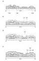
<半導体装置の構成例>
図1(A)は、本発明の一態様の半導体装置の上面図であり、図1(B)は、図1(A
)の一点鎖線A−B間及び一点鎖線C−D間における切断面の断面図に相当する。なお、
図1(A)において、煩雑になることを避けるため、半導体装置の構成要素の一部(ゲー
ト絶縁膜として機能する絶縁膜等)を省略して図示している。<Semiconductor device configuration example>
FIG. 1 (A) is a top view of the semiconductor device according to one aspect of the present invention, and FIG. 1 (B) is FIG. 1 (A).
) Corresponds to the cross-sectional view of the cut surface between the alternate long and short dash lines AB and between the alternate long and short dash lines CD. note that,
In FIG. 1A, in order to avoid complication, a part of the components of the semiconductor device (an insulating film that functions as a gate insulating film, etc.) is omitted.
図1(A)、(B)に示す半導体装置は、トランジスタ150と、接続部160とを有
する。The semiconductor device shown in FIGS. 1A and 1B has a
トランジスタ150は、基板102上のゲート電極104aと、ゲート電極104a上
に形成される第1の絶縁膜108と、第1の絶縁膜108上に形成され、ゲート電極10
4aと重畳する位置に形成される酸化物半導体膜110と、酸化物半導体膜110と電気
的に接続されるソース電極112a及びドレイン電極112bとを有している。The
It has an
また、図1(B)においては、第1の絶縁膜108は、絶縁膜106と絶縁膜107の
2層の積層構造を例示している。なお、第1の絶縁膜108の構造はこれに限定されず、
例えば、単層構造または3層以上の積層構造としてもよい。Further, in FIG. 1B, the first insulating
For example, it may be a single-layer structure or a laminated structure of three or more layers.
また、トランジスタ150上、より詳しくは酸化物半導体膜110、ソース電極112
a、及びドレイン電極112b上に第2の絶縁膜120が形成されている。図1(B)に
おいては、第2の絶縁膜120として、絶縁膜114、116、118の3層の積層構造
を例示している。なお、第2の絶縁膜120の構造はこれに限定されず、例えば、単層構
造、2層の積層構造、または4層以上の積層構造としてもよい。Further, on the
A second
また、第2の絶縁膜120には、ドレイン電極112bに達する開口142aが形成さ
れている。また、第2の絶縁膜120上に開口142aを覆うように画素電極として機能
する導電膜122aが形成されている。なお、導電膜122aは、トランジスタ150の
ドレイン電極112bと接続される。Further, the second
接続部160は、基板102上の第1の配線104bと、第1の配線104b上の第1
の絶縁膜108と、第1の絶縁膜108に設けられる開口142bと、第1の絶縁膜10
8上の第2の配線112cと、第2の配線112c上の第2の絶縁膜120と、第2の絶
縁膜120に設けられる開口140と、開口142b及び開口140を覆うように形成さ
れ、且つ第1の配線104bと第2の配線112cを接続する第3の配線として機能する
導電膜122bと、を有する。なお、図1(B)において、第1の配線104b上の開口
は、開口140と開口142bの2段階の開口形状について例示したが、これに限定され
ない。例えば、開口142bの工程で一括して開口し第1の配線104bに達する開口を
形成してもよい。The
The insulating
It is formed so as to cover the
なお、第1の配線104bは、トランジスタ150のゲート電極104aと同一工程で
形成される。別言すると、第1の配線104bは、トランジスタ150のゲート電極10
4aと同一表面上に形成される。また、第2の配線112cは、トランジスタ150のソ
ース電極112a及びドレイン電極112bと同一工程で形成される。別言すると、第2
の配線112cは、トランジスタ150のソース電極112a及びドレイン電極112b
と同一表面上に形成される。The
It is formed on the same surface as 4a. Further, the
The
Is formed on the same surface as.
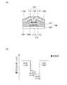
ここで、図1(B)に示す半導体装置のトランジスタ150及び接続部160の一部を
拡大した図を図2(A)、(B)に示す。図2(A)は、トランジスタ150のソース電
極112a及びドレイン電極112bの一部の拡大図を示し、図2(B)は、接続部16
0の第2の配線112cの一部の拡大図を示している。Here, FIGS. 2 (A) and 2 (B) show enlarged views of a part of the
An enlarged view of a part of the
図2(A)に示すようにトランジスタ150のソース電極112a及びドレイン電極1
12bの端部は、下端部α1と上端部α2を有している。なお、図2(A)において、ソ
ース電極112aにのみ下端部α1と上端部α2を図示しているが、ドレイン電極112
bも同様の構成である。As shown in FIG. 2A, the
The end portion of 12b has a lower end portion α1 and an upper end portion α2 . In FIG. 2A, the lower end portion α1 and the upper end portion α2 are shown only on the
b also has the same configuration.
また、図2(B)に示すように接続部160の第2の配線112cの端部は、下端部β
1と上端部β2を有している。なお、図2(B)において、第2の配線112cの端部の
一方のみ下端部β1と上端部β2を図示しているが、第2の配線112cの他方の端部も
同様の構成である。ただし、第2の配線112cの端部の形状は、図2(B)に示す構造
に限定されず、例えば、第2の配線112cのいずれか一方の端部のみ図2(B)に示す
構成と同様であればよい。Further, as shown in FIG. 2B, the end portion of the
It has 1 and the upper end β2 . In FIG. 2B, only one of the ends of the
図2(A)、(B)に示すように、トランジスタ150が有するソース電極112a及
びドレイン電極112bの端部の距離(α1−α2間の距離)よりも、接続部160が有
する第2の配線112cが有する端部の距離(β1−β2間の距離)の方が長い。As shown in FIGS. 2A and 2B, the distance between the ends of the
第2の配線112cの端部をソース電極112a及びドレイン電極112bの端部より
も上端部と下端部の距離を長くすることによって、第2の配線112cに起因する段差を
低減することができる。第2の配線112cに起因する段差を低減することによって、第
2の配線112cの上方に形成される絶縁膜114、116、118及び/または第3の
配線として機能する導電膜122bの被覆性を向上させることができる。これによって、
第2の配線112cと第3の配線として機能する導電膜122bの接触不良を低減するこ
とができる。By making the distance between the upper end and the lower end of the
It is possible to reduce poor contact between the
また、トランジスタ150が有するソース電極112a及びドレイン電極112bの端
部は、第2の配線112cの端部よりも上端部と下端部の距離が短い。このような構造と
することで、該トランジスタに良好な電気特性を付与することができる。図1(B)及び
図2(A)に示すようにトランジスタ150がチャネルエッチ型のトランジスタ構造の場
合、ソース電極112a及びドレイン電極112bの形成時において、酸化物半導体膜1
10にダメージが入り得る。Further, the distance between the upper end and the lower end of the
10 can be damaged.
例えば、ソース電極112a及びドレイン電極112b、並びに第2の配線112cの
形成時において、エッチング条件を調整することによって、ソース電極112a及びドレ
イン電極112b、並びに第2の配線112cの各端部の形状を調整することが可能とな
るが、ソース電極112a及びドレイン電極112bの端部の形状を第2の配線112c
と同様の端部の形状とすることで、エッチング時間が長くなり酸化物半導体膜110にダ
メージが入り得る。したがって、ダメージが入った酸化物半導体膜110を有するトラン
ジスタ150は、安定した電気特性が得られない場合がある。また、ソース電極112a
及びドレイン電極112bの間の距離によって、トランジスタ150のチャネル長(L)
が決まるため、ソース電極112a及びドレイン電極112bの端部の形状を調整するこ
とで、基板面内でのチャネル長(L)がばらつく要因となる場合がある。For example, when the
By making the shape of the end portion similar to the above, the etching time becomes long and the
And the channel length (L) of the
Therefore, adjusting the shapes of the ends of the
しかしながら、本発明の一態様の半導体装置においては、トランジスタが有するソース
電極及びドレイン電極の端部の形状と、接続部が有する配線の端部の形状を異ならせるこ
とで、トランジスタの安定した電気特性と、接続部の良好な接触抵抗とを両方満たすこと
が可能となる。これは、本発明の一態様の半導体装置で得られる優れた効果である。However, in the semiconductor device of one aspect of the present invention, the shape of the end of the source electrode and the drain electrode of the transistor is different from the shape of the end of the wiring of the connection, so that the stable electrical characteristics of the transistor are stable. And good contact resistance of the connection part can be satisfied. This is an excellent effect obtained by the semiconductor device of one aspect of the present invention.
また、本発明の一態様の半導体装置においては、トランジスタのソース電極及びドレイ
ン電極の形成と、接続部の配線の形成を同一のマスクを用いて、一括して形成することが
できる。したがって、生産性の優れた半導体装置を提供することができる。Further, in the semiconductor device of one aspect of the present invention, the formation of the source electrode and the drain electrode of the transistor and the formation of the wiring of the connection portion can be collectively formed by using the same mask. Therefore, it is possible to provide a semiconductor device having excellent productivity.
ここで、図2(B)に示す接続部160の変形例について、図2(C)、(D)を用い
て説明を行う。Here, a modified example of the
図2(C)は、図2(B)に示す接続部の変形例であり、第2の配線112cの端部の
形状が異なる。また、第2の配線112cの端部の形状の違いに伴い、上方に形成される
絶縁膜114、116、118の形状も異なる。FIG. 2C is a modified example of the connection portion shown in FIG. 2B, and the shape of the end portion of the
図2(C)に示す接続部160の端部は、下端部β3と上端部β5の間に、中端部β4
を有する。このように、第2の配線112cの端部の形状は、複数の角度を持った階段状
の形状としてもよい。このように複数の角度を持った階段状の形状とすることによって、
上方に形成される絶縁膜114、116、118の被覆性をさらに向上させることができ
る。The end of the
Have. As described above, the shape of the end portion of the
The coverage of the insulating
また、図2(C)に示す接続部160の端部においては、中端部β4と上端部β5は、
曲率を有する。このように、端部において曲率を有する構造とすることで、上方に形成さ
れる絶縁膜114、116、118の被覆性をさらに向上させることができる。Further, in the end portion of the
Has a curvature. As described above, by forming the structure having a curvature at the end portion, the covering property of the insulating
次に、図2(D)は、図2(B)に示す接続部の変形例であり、第2の配線112cの
端部の形状が異なる。また、第2の配線112cの端部の形状の違いに伴い、上方に形成
される絶縁膜114、116、118の形状も異なる。Next, FIG. 2D is a modified example of the connection portion shown in FIG. 2B, and the shape of the end portion of the
図2(D)に示す接続部160の端部は、下端部β6と上端部β11の間に、中端部β
7、β8、β9、β10とを有する。例えば、第2の配線112cの積層構造が、図2(
D)に示すように、第2の配線112c_1、第2の配線112c_2、第2の配線11
2c_3の3層の積層構造とすることで、下端部β6と上端部β11の間に、中端部β7
、β8、β9、β10とを有する構造とすることができる。このように、第2の配線11
2cとしては、少なくとも2層以上の積層構造とすると好ましい。The end of the
It has 7 , β8 , β9 , and β10 . For example, the laminated structure of the
As shown in D), the second wiring 112c_1, the second wiring 112c_2, and the
By forming a three-layer laminated structure of 2c_3, the middle end β7 islocated between the lower end β 6 and the upper end β11.
, Β8 , β9 , and β10 can be formed. In this way, the
As 2c, it is preferable to have a laminated structure of at least two layers or more.
図2(A)、(B)、(C)、(D)に示すように、本発明の一態様の半導体装置は、
少なくともトランジスタ150が有するソース電極112a及びドレイン電極112bの
上端部と下端部の距離(α1−α2の距離)よりも、接続部160が有する第2の配線1
12cの上端部と下端部の距離(β1−β2の距離、β3−β5の距離、またはβ6−β
11の距離)の方が、長ければよい。As shown in FIGS. 2 (A), 2 (B), (C), and (D), the semiconductor device according to one aspect of the present invention is
The
The distance between the upper and lower ends of 12c (distance of β1- β2 , distance of β3- β5 , or β6- β
The distance of 11 ) should be longer.
ただし、図2(A)乃至(D)に示すようにソース電極112a及びドレイン電極11
2b、並びに第2の配線112cにおいて、上端部は下端部よりも内側に設けられている
必要がある。However, as shown in FIGS. 2A to 2D, the
In 2b and the
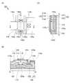
<接続部の上面形状(変形例)>
ここで、図1(A)に示す接続部160の上面形状の変形例について、図3を用いて説
明を行う。<Top surface shape of connection part (deformation example)>
Here, a modified example of the upper surface shape of the connecting
図3(A)は、第1の配線104bと、第2の配線112cが第3の配線として機能す
る導電膜122bを介して接続している。In FIG. 3A, the
図3(A)に示すように、第1の配線104b及び第2の配線112cの先端の上面形
状を円形とすることもできる。また、図示しないが、円形以外にも楕円または多角形の形
状と直線とを組み合わせた上面形状としてもよい。As shown in FIG. 3A, the upper surface shape of the tip of the
図3(A)に示すように、第1の配線104b及び第2の配線112cの先端の上面形
状を円形とすることで、半導体装置の作製工程中で生じうるゴミ(パーティクルともいう
)が端部に溜まることを抑制することが可能となる。したがって、第3の配線として機能
する第2の配線112cが開口140、142b、142cを良好に被覆することが可能
となる。As shown in FIG. 3A, by making the upper surface shape of the tip of the
また、図1(A)、及び図3(A)においては、第1の配線104bと第2の配線11
2cを互いに平行に延伸するような構成を例示していたが、図3(B)に示すように、第
1の配線104bと第2の配線112cを互いに対向するように配置してもよい。また、
図3(C)に示すように、第1の配線104bと第2の配線112cを互いに直角に対峙
するように配置してもよい。図3(A)、(B)、(C)に示すように第1の配線104
bと第2の配線112cの上面形状及び配置方法については、実施者が適宜最適な上面形
状及び配置とすればよい。Further, in FIGS. 1 (A) and 3 (A), the
Although the configuration in which the 2c is extended in parallel with each other has been illustrated, the
As shown in FIG. 3C, the
Regarding the top surface shape and arrangement method of b and the
また、図3(B)、(C)において、第2の配線112cの上方に、それぞれ領域14
4a、及び領域144bを配置する構成を例示している。Further, in FIGS. 3B and 3C, the regions 14 are located above the
The configuration in which the 4a and the
図3(B)、(C)に示す領域144a、144bは、第2の配線112cの端部の一
部の上端部と下端部の距離がトランジスタ150が有するソース電極112a及びドレイ
ン電極112bの端部の上端部と下端部の距離よりも長くなる領域である。例えば、第2
の配線112c形成時において、フォトリソグラフィ工程により、グレートーンマスク等
の露光マスクを用いて、第2の配線112cを加工することによって、第2の配線112
cの端部の一部の形状を図1(B)、及び図2(B)、(C)、(D)に示す構造とする
ことができる。In the
When the
The shape of a part of the end portion of c can be the structure shown in FIGS. 1 (B) and 2 (B), (C), and (D).
なお、図1(A)、(B)に示す本発明の一態様の半導体装置の詳細については、半導
体装置の作製方法にその詳細を記載する。The details of the semiconductor device according to one aspect of the present invention shown in FIGS. 1A and 1B will be described in the method for manufacturing the semiconductor device.
<半導体装置の作製方法>
図1(A)、(B)に示す本発明の一態様の半導体装置の作製方法について、図4乃至
図6を用いて以下詳細に説明する。<Method of manufacturing semiconductor devices>
The method for manufacturing the semiconductor device according to one aspect of the present invention shown in FIGS. 1 (A) and 1 (B) will be described in detail below with reference to FIGS. 4 to 6.
まず、基板102を準備する。基板102としては、アルミノシリケートガラス、アル
ミノホウケイ酸ガラス、バリウムホウケイ酸ガラスなどのガラス材料を用いる。量産する
上では、基板102は、第8世代(2160mm×2460mm)、第9世代(2400
mm×2800mm、または2450mm×3050mm)、第10世代(2950mm
×3400mm)等のマザーガラスを用いることが好ましい。マザーガラスは、処理温度
が高く、処理時間が長いと大幅に収縮するため、マザーガラスを使用して量産を行う場合
、作製工程の加熱処理は、好ましくは600℃以下、さらに好ましくは450℃以下、さ
らに好ましくは350℃以下とすることが望ましい。First, the
mm x 2800 mm, or 2450 mm x 3050 mm), 10th generation (2950 mm)
It is preferable to use a mother glass (× 3400 mm) or the like. Since mother glass shrinks significantly when the treatment temperature is high and the treatment time is long, when mass production is performed using mother glass, the heat treatment in the manufacturing process is preferably 600 ° C. or lower, more preferably 450 ° C. or lower. More preferably, the temperature is 350 ° C. or lower.
次に、基板102上に導電膜を形成し、該導電膜を所望の領域に加工することで、ゲー
ト電極104a、及び第1の配線104bを形成する。その後、基板102、ゲート電極
104a、及び第1の配線104b上に絶縁膜106及び絶縁膜107を含む第1の絶縁
膜108を形成する(図4(A)参照)。Next, a conductive film is formed on the
なお、ゲート電極104a及び第1の配線104bを形成する工程は、第1のパターニ
ング工程となる。The step of forming the
ゲート電極104a及び第1の配線104bに用いる材料としては、アルミニウム、ク
ロム、銅、タンタル、チタン、モリブデン、タングステンから選ばれた金属元素、または
上述した金属元素を成分とする合金か、上述した金属元素を組み合わせた合金等を用いて
形成することができる。また、ゲート電極104a及び第1の配線104bに用いる材料
は、単層構造でも、二層以上の積層構造としてもよい。例えば、アルミニウム膜上にチタ
ン膜を積層する二層構造、窒化チタン膜上にチタン膜を積層する二層構造、窒化チタン膜
上にタングステン膜を積層する二層構造、窒化タンタル膜または窒化タングステン膜上に
タングステン膜を積層する二層構造、チタン膜と、そのチタン膜上にアルミニウム膜を積
層し、さらにその上にチタン膜を形成する三層構造等がある。また、アルミニウムに、チ
タン、タンタル、タングステン、モリブデン、クロム、ネオジム、スカンジウムから選ば
れた元素の膜、または複数組み合わせた合金膜、もしくは窒化膜を用いてもよい。また、
ゲート電極104a及び第1の配線104bに用いる材料としては、例えば、スパッタリ
ング法を用いて形成することができる。The material used for the
The material used for the
絶縁膜106としては、例えば、窒化酸化シリコン膜、窒化シリコン膜、酸化アルミニ
ウム膜などを用いればよく、PE−CVD装置を用いて積層または単層で設ける。また、
絶縁膜106を積層構造とした場合、第1の窒化シリコン膜として、欠陥が少ない窒化シ
リコン膜とし、第1の窒化シリコン膜上に、第2の窒化シリコン膜として、水素放出量及
びアンモニア放出量の少ない窒化シリコン膜を設けると好適である。この結果、絶縁膜1
06に含まれる水素及び窒素が、後に形成される酸化物半導体膜110へ移動または拡散
することを抑制できる。As the insulating
When the insulating
It is possible to prevent hydrogen and nitrogen contained in 06 from moving or diffusing to the
絶縁膜107としては、酸化シリコン膜、酸化窒化シリコン膜などを用いればよく、P
E−CVD装置を用いて積層または単層で設ける。As the insulating
It is provided in a laminated or single layer using an E-CVD apparatus.
また、第1の絶縁膜108としては、絶縁膜106として、例えば、厚さ400nmの
窒化シリコン膜を形成し、その後、絶縁膜107として、厚さ50nmの酸化窒化シリコ
ン膜を形成する積層構造を用いることができる。該窒化シリコン膜と、該酸化窒化シリコ
ン膜は、真空中で連続して形成すると不純物の混入が抑制され好ましい。なお、ゲート電
極104aと重畳する位置の第1の絶縁膜108は、トランジスタ150のゲート絶縁膜
として機能する。また、窒化酸化シリコンとは、窒素の含有量が酸素の含有量より大きい
絶縁材料であり、他方、酸化窒化シリコンとは、酸素の含有量が窒素の含有量より大きな
絶縁材料のことをいう。Further, as the first insulating
ゲート絶縁膜として、上記のような構成とすることで、例えば以下のような効果を得る
ことができる。窒化シリコン膜は、酸化シリコン膜と比較して比誘電率が高く、同等の静
電容量を得るのに必要な膜厚が大きいため、ゲート絶縁膜を物理的に厚膜化することがで
きる。よって、トランジスタ150の絶縁耐圧の低下を抑制、さらには絶縁耐圧を向上さ
せて、トランジスタ150の静電破壊を抑制することができる。By forming the gate insulating film as described above, for example, the following effects can be obtained. Since the silicon nitride film has a higher relative permittivity than the silicon oxide film and the film thickness required to obtain the same capacitance is large, the gate insulating film can be physically thickened. Therefore, it is possible to suppress a decrease in the withstand voltage of the
次に、第1の絶縁膜108上に酸化物半導体膜を形成し、該酸化物半導体膜を所望の領
域に加工することで、酸化物半導体膜110を形成する(図4(B)参照)。Next, an oxide semiconductor film is formed on the first insulating
なお、酸化物半導体膜110を形成する工程は、第2のパターニング工程となる。 The step of forming the
酸化物半導体膜110としては、少なくともインジウム(In)、亜鉛(Zn)及びM
(Al、Ga、Ge、Y、Zr、Sn、La、CeまたはHf等の金属)を含むIn−M
−Zn酸化物で表記される膜を含むことが好ましい。または、InとZnの双方を含むこ
とが好ましい。また、該酸化物半導体を用いたトランジスタの電気特性のばらつきを減ら
すため、それらと共に、スタビライザーを含むことが好ましい。The
In-M containing (metals such as Al, Ga, Ge, Y, Zr, Sn, La, Ce or Hf)
It is preferable to include a film represented by −Zn oxide. Alternatively, it is preferable to contain both In and Zn. Further, in order to reduce variations in the electrical characteristics of the transistor using the oxide semiconductor, it is preferable to include a stabilizer together with them.
スタビライザーとしては、ガリウム(Ga)、スズ(Sn)、ハフニウム(Hf)、ア
ルミニウム(Al)、またはジルコニウム(Zr)等がある。また、他のスタビライザー
としては、ランタノイドである、ランタン(La)、セリウム(Ce)、プラセオジム(
Pr)、ネオジム(Nd)、サマリウム(Sm)、ユウロピウム(Eu)、ガドリニウム
(Gd)、テルビウム(Tb)、ジスプロシウム(Dy)、ホルミウム(Ho)、エルビ
ウム(Er)、ツリウム(Tm)、イッテルビウム(Yb)、ルテチウム(Lu)等があ
る。Examples of the stabilizer include gallium (Ga), tin (Sn), hafnium (Hf), aluminum (Al), zirconium (Zr) and the like. Other stabilizers include lanthanoids such as lanthanum (La), cerium (Ce), and praseodymium (
Pr), Neogym (Nd), Samarium (Sm), Europium (Eu), Gadolinium (Gd), Terbium (Tb), Dysprosium (Dy), Holmium (Ho), Elbium (Er), Thulium (Tm), Ytterbium (Tm) There are Yb), lutetium (Lu) and the like.
酸化物半導体膜110を構成する酸化物半導体として、例えば、In−Ga−Zn系酸
化物、In−Al−Zn系酸化物、In−Sn−Zn系酸化物、In−Hf−Zn系酸化
物、In−La−Zn系酸化物、In−Ce−Zn系酸化物、In−Pr−Zn系酸化物
、In−Nd−Zn系酸化物、In−Sm−Zn系酸化物、In−Eu−Zn系酸化物、
In−Gd−Zn系酸化物、In−Tb−Zn系酸化物、In−Dy−Zn系酸化物、I
n−Ho−Zn系酸化物、In−Er−Zn系酸化物、In−Tm−Zn系酸化物、In
−Yb−Zn系酸化物、In−Lu−Zn系酸化物、In−Sn−Ga−Zn系酸化物、
In−Hf−Ga−Zn系酸化物、In−Al−Ga−Zn系酸化物、In−Sn−Al
−Zn系酸化物、In−Sn−Hf−Zn系酸化物、In−Hf−Al−Zn系酸化物を
用いることができる。Examples of the oxide semiconductor constituting the
In-Gd-Zn-based oxide, In-Tb-Zn-based oxide, In-Dy-Zn-based oxide, I
n-Ho-Zn-based oxide, In-Er-Zn-based oxide, In-Tm-Zn-based oxide, In
-Yb-Zn-based oxide, In-Lu-Zn-based oxide, In-Sn-Ga-Zn-based oxide,
In-Hf-Ga-Zn-based oxide, In-Al-Ga-Zn-based oxide, In-Sn-Al
-Zn-based oxides, In-Sn-Hf-Zn-based oxides, and In-Hf-Al-Zn-based oxides can be used.
なお、ここで、In−Ga−Zn系酸化物とは、InとGaとZnを主成分として有す
る酸化物という意味であり、InとGaとZnの比率は問わない。また、InとGaとZ
n以外の金属元素が入っていてもよい。Here, the In-Ga-Zn-based oxide means an oxide containing In, Ga, and Zn as main components, and the ratio of In, Ga, and Zn does not matter. Also, In, Ga and Z
A metal element other than n may be contained.
酸化物半導体膜110の成膜方法は、スパッタリング法、MBE(Molecular
Beam Epitaxy)法、CVD法、パルスレーザ堆積法、ALD(Atomi
c Layer Deposition)法等を適宜用いることができる。とくに、酸化
物半導体膜110を成膜する際、スパッタリング法を用いると緻密な膜が形成されるため
、好適である。The film forming method of the
Beam Epitaxy) method, CVD method, pulse laser deposition method, ALD (Atomi)
c Layer Deposition) method or the like can be appropriately used. In particular, when the
酸化物半導体膜110として、酸化物半導体膜を成膜する際、できる限り膜中に含まれ
る水素濃度を低減させることが好ましい。水素濃度を低減させるには、例えば、スパッタ
リング法を用いて成膜を行う場合には、成膜室内を高真空排気するのみならずスパッタガ
スの高純度化も必要である。スパッタガスとして用いる酸素ガスやアルゴンガスは、露点
が−40℃以下、好ましくは−80℃以下、より好ましくは−100℃以下、より好まし
くは−120℃以下にまで高純度化したガスを用いることで酸化物半導体膜に水分等が取
り込まれることを可能な限り防ぐことができる。When forming the oxide semiconductor film as the
また、成膜室内の残留水分を除去するためには、吸着型の真空ポンプ、例えば、クライ
オポンプ、イオンポンプ、チタンサブリメーションポンプを用いることが好ましい。また
、ターボ分子ポンプにコールドトラップを加えたものであってもよい。クライオポンプは
、例えば、水素分子、水(H2O)など水素原子を含む化合物、炭素原子を含む化合物等
の排気能力が高いため、クライオポンプを用いて排気した成膜室で成膜した膜中に含まれ
る不純物の濃度を低減できる。Further, in order to remove residual moisture in the film forming chamber, it is preferable to use an adsorption type vacuum pump, for example, a cryopump, an ion pump, or a titanium sublimation pump. Further, a turbo molecular pump to which a cold trap is added may be used. Cryopump, a compound containing hydrogen molecules, such as water (H 2O) a hydrogen atom, have high evacuation capability, such as a compound containing a carbon atom, a film was formed in the deposition chamber evacuated using a cryopump The concentration of impurities contained therein can be reduced.
また、酸化物半導体膜110として、酸化物半導体膜をスパッタリング法で成膜する場
合、成膜に用いる金属酸化物ターゲットの相対密度(充填率)は90%以上100%以下
、好ましくは95%以上100%以下とする。相対密度の高い金属酸化物ターゲットを用
いることにより、成膜される膜を緻密な膜とすることができる。When the
なお、基板102を高温に保持した状態で酸化物半導体膜110として、酸化物半導体
膜を形成することも、酸化物半導体膜中に含まれうる不純物濃度を低減するのに有効であ
る。基板102を加熱する温度としては、150℃以上450℃以下とすればよく、好ま
しくは基板温度が200℃以上350℃以下とすればよい。Forming the oxide semiconductor film as the
次に、第1の加熱処理を行うことが好ましい。第1の加熱処理は、250℃以上650
℃以下、好ましくは300℃以上500℃以下の温度で、不活性ガス雰囲気、酸化性ガス
を10ppm以上含む雰囲気、または減圧状態で行えばよい。また、第1の加熱処理の雰
囲気は、不活性ガス雰囲気で加熱処理した後に、脱離した酸素を補うために酸化性ガスを
10ppm以上含む雰囲気で行ってもよい。第1の加熱処理によって、酸化物半導体膜1
10に用いる酸化物半導体の結晶性を高め、さらに第1の絶縁膜108及び酸化物半導体
膜110から水素や水などの不純物を除去することができる。なお、酸化物半導体膜11
0を島状に加工する前に第1の加熱工程を行ってもよい。Next, it is preferable to perform the first heat treatment. The first heat treatment is 250 ° C. or higher and 650 ° C.
The operation may be carried out at a temperature of ° C. or lower, preferably 300 ° C. or higher and 500 ° C. or lower, in an atmosphere of an inert gas, an atmosphere containing 10 ppm or more of an oxidizing gas, or a reduced pressure state. Further, the atmosphere of the first heat treatment may be an atmosphere containing 10 ppm or more of an oxidizing gas in order to supplement the desorbed oxygen after the heat treatment in an inert gas atmosphere. By the first heat treatment, the
The crystallinity of the oxide semiconductor used in No. 10 can be enhanced, and impurities such as hydrogen and water can be removed from the first insulating
The first heating step may be performed before processing 0 into an island shape.
次に、第1の絶縁膜108及び酸化物半導体膜110上にソース電極112a、ドレイ
ン電極112b、及び第2の配線112cとなる導電膜112を形成する(図4(C)参
照)。Next, a
ソース電極112a、ドレイン電極112b、及び第2の配線112cに用いることの
できる導電膜112の材料としては、アルミニウム、チタン、クロム、ニッケル、銅、イ
ットリウム、ジルコニウム、モリブデン、銀、タンタル、またはタングステンからなる単
体金属、またはこれを主成分とする合金を単層構造または積層構造として用いることがで
きる。とくに、アルミニウム、クロム、銅、タンタル、チタン、モリブデン、タングステ
ンの中から選択される一以上の元素を含むと好ましい。例えば、アルミニウム膜上にチタ
ン膜を積層する二層構造、タングステン膜上にチタン膜を積層する二層構造、銅−マグネ
シウム−アルミニウム合金膜上に銅膜を積層する二層構造、チタン膜または窒化チタン膜
と、そのチタン膜または窒化チタン膜上に重ねてアルミニウム膜または銅膜を積層し、さ
らにその上にチタン膜または窒化チタン膜を形成する三層構造、モリブデン膜または窒化
モリブデン膜と、そのモリブデン膜または窒化モリブデン膜上に重ねてアルミニウム膜ま
たは銅膜を積層し、さらにその上にモリブデン膜または窒化モリブデン膜を形成する三層
構造等がある。なお、酸化インジウム、酸化錫または酸化亜鉛を含む透明導電材料を用い
てもよい。また、導電膜は、例えば、スパッタリング法を用いて形成することができる。The material of the
次に、導電膜112上の所望の領域にレジストマスク148a、148b、148cを
形成する(図4(D)参照)。Next, resist
レジストマスク148a、148b、148cについては、感光性の樹脂を導電膜11
2上に形成した後、グレートーンマスクまたはハーフトーンマスクを用いて露光すること
で、第2の配線112cとなる領域のレジストマスク148cのみ階段状の形状とするこ
とができる。For the resist
After forming on the two, by exposing with a gray tone mask or a halftone mask, only the resist
グレートーンマスクまたはハーフトーンマスクとしては、例えば、図3(B)、(C)
に示すような領域144a、144bに位置する領域に適用することができる。Examples of the gray tone mask or halftone mask include FIGS. 3 (B) and 3 (C).
It can be applied to the region located in the
次に、レジストマスク148a、148b、148c上から導電膜112のエッチング
処理を行い、エッチング後にレジストマスク148a、148b、148cを除去するこ
とで、ソース電極112a、ドレイン電極112b、及び第2の配線112cを形成する
(図5(A)参照)。Next, the
なお、ソース電極112a、ドレイン電極112b、及び第2の配線112cを形成す
る工程は、第3のパターニング工程となる。The step of forming the
このように、ソース電極112a、ドレイン電極112b、及び第2の配線112cを
同一の工程で形成し、且つソース電極112a及びドレイン電極112bと、第2の配線
112cの端部を異なる形状とすることができる。In this way, the
また、本実施の形態においては、導電膜112のエッチングには、ドライエッチング法
を用いる。Further, in the present embodiment, a dry etching method is used for etching the
なお、導電膜112のエッチングの際に、酸化物半導体膜110の一部が消失し、凹部
を有する酸化物半導体膜110となる場合がある。When the
また、酸化物半導体膜110上にソース電極112a及びドレイン電極112bが形成
された段階で、トランジスタ150が形成される。Further, the
次に、第1の絶縁膜108、酸化物半導体膜110、ソース電極112a、ドレイン電
極112b、及び第2の配線112c上に絶縁膜114、116を形成する(図5(B)
参照)。Next, the insulating
reference).
絶縁膜114、116としては、酸化物半導体膜110として用いる酸化物半導体との
界面特性を向上させるため、酸素を含む無機絶縁材料を用いることができる。酸素を含む
無機絶縁材料としては、例えば酸化シリコン膜、または酸化窒化シリコン膜等が挙げられ
る。また、絶縁膜114、116としては、例えば、PE−CVD法を用いて形成するこ
とができる。As the insulating
絶縁膜114の厚さは、5nm以上150nm以下、好ましくは5nm以上50nm以
下、好ましくは10nm以上30nm以下とすることができる。絶縁膜116の厚さは、
30nm以上500nm以下、好ましくは150nm以上400nm以下とすることがで
きる。The thickness of the insulating
It can be 30 nm or more and 500 nm or less, preferably 150 nm or more and 400 nm or less.
また、絶縁膜114、116は、同種の材料の絶縁膜を用いることができるため、絶縁
膜114と絶縁膜116の界面が明確に確認できない場合がある。したがって、本実施の
形態においては、絶縁膜114と絶縁膜116の界面は、破線で図示している。なお、本
実施の形態においては、絶縁膜114と絶縁膜116の2層構造について、説明したが、
これに限定されず、例えば、絶縁膜114の単層構造、絶縁膜116の単層構造、または
3層以上の積層構造としてもよい。Further, since the insulating
The present invention is not limited to this, and for example, a single-layer structure of the insulating
次に、絶縁膜114、116の所望の領域を加工することで、開口140を形成する(
図5(C)参照)。Next, the
(See FIG. 5 (C)).
なお、開口140を形成する工程は、第4のパターニング工程となる。 The step of forming the
なお、開口140としては、少なくとも絶縁膜107が露出するように形成する。本実
施の形態においては、開口140によって、絶縁膜107の表面の一部が露出している。
開口140の形成方法としては、例えば、ドライエッチング法を用いることができる。た
だし、開口140の形成方法としては、これに限定されず、ウェットエッチング法、また
はドライエッチング法とウェットエッチング法を組み合わせた形成方法としてもよい。The
As a method for forming the
次に、絶縁膜116上、及び開口140を覆うように絶縁膜118を形成する。絶縁膜
118の形成によって、トランジスタ150上に絶縁膜114、116、118を含む第
2の絶縁膜120が形成される(図5(D)参照)。Next, the insulating
絶縁膜118は、外部からの不純物、例えば、水、アルカリ金属、アルカリ土類金属等
が、酸化物半導体膜110へ拡散するのを防ぐ材料で形成される膜であり、更には水素を
含む。The insulating
絶縁膜118の一例としては、厚さ150nm以上400nm以下の窒化シリコン膜、
窒化酸化シリコン膜等を用いることができる。本実施の形態においては、絶縁膜118と
して、厚さ150nmの窒化シリコン膜を用いる。As an example of the insulating
A silicon nitride film or the like can be used. In the present embodiment, a silicon nitride film having a thickness of 150 nm is used as the insulating
また、上記窒化シリコン膜は、不純物等からのブロック性を高めるために、高温で成膜
されることが好ましく、例えば基板温度100℃以上基板の歪み点以下、より好ましくは
300℃以上400℃以下の温度で加熱して成膜することが好ましい。また高温で成膜す
る場合は、酸化物半導体膜110として用いる酸化物半導体から酸素が脱離し、キャリア
濃度が上昇する現象が発生することがあるため、このような現象が発生しない温度とする
。Further, the silicon nitride film is preferably formed at a high temperature in order to improve the blocking property from impurities and the like. For example, the substrate temperature is 100 ° C. or higher and the strain point of the substrate or lower, more preferably 300 ° C. or higher and 400 ° C. or lower. It is preferable to heat the film at the above temperature to form a film. Further, when the film is formed at a high temperature, oxygen may be desorbed from the oxide semiconductor used as the
なお、図5(D)において、図示しないが、絶縁膜118の上方にさらに、絶縁膜を形
成してもよい。該絶縁膜としては、例えば、有機シランガスを用いたPE−CVD法によ
り形成した酸化シリコン膜を用いることができる。当該酸化シリコン膜は300nm以上
600nm以下で設けることができる。有機シランガスとしては、珪酸エチル(TEOS
:化学式Si(OC2H5)4)、テトラメチルシラン(TMS:化学式Si(CH3)
4)、テトラメチルシクロテトラシロキサン(TMCTS)、オクタメチルシクロテトラ
シロキサン(OMCTS)、ヘキサメチルジシラザン(HMDS)、トリエトキシシラン
(SiH(OC2H5)3)、トリスジメチルアミノシラン(SiH(N(CH3)2)
3)などのシリコン含有化合物を用いることができる。また、上記酸化シリコン膜は、例
えば、有機シランガスと酸素を用い、基板温度を200℃以上550℃以下、好ましくは
220℃以上500℃以下、より好ましくは300℃以上450℃以下としたPE−CV
D法により形成することができる。Although not shown in FIG. 5D, an insulating film may be further formed above the insulating
: Chemical formula Si (OC2 H5 )4 ), Tetramethylsilane (TMS: Chemical formula Si (CH3 ))
4), tetramethylcyclotetrasiloxane (TMCTS), octamethylcyclotetrasiloxane (OMCTS), hexamethyldisilazane (HMDS), triethoxysilane(SiH (OC 2 H 5) 3), trisdimethylaminosilane (SiH (N (CH3 )2 )
Silicon-containing compounds such as3) can be used. Further, the silicon oxide film uses, for example, organic silane gas and oxygen, and the substrate temperature is 200 ° C. or higher and 550 ° C. or lower, preferably 220 ° C. or higher and 500 ° C. or lower, and more preferably 300 ° C. or higher and 450 ° C. or lower.
It can be formed by the D method.
絶縁膜118上にさらに上述した絶縁膜を形成することによって、トランジスタ150
等に起因する凹凸を平坦化することが可能となる。また、上述した絶縁膜は無機材料によ
り形成されるため、有機材料を用いる平坦化樹脂膜等と比較し、酸化物半導体膜110に
影響を与える不純物が少ないので好適である。By further forming the above-mentioned insulating film on the insulating
It is possible to flatten the unevenness caused by the above. Further, since the above-mentioned insulating film is formed of an inorganic material, it is suitable because it has less impurities affecting the
次に、絶縁膜114、116、118の所望の領域を加工することで、開口142a、
142b、142cを形成する(図6(A)参照)。Next, by processing the desired regions of the insulating
142b and 142c are formed (see FIG. 6 (A)).
なお、開口142a、142b、142cを形成する工程は、第5のパターニング工程
となる。The step of forming the
開口142aとしては、ドレイン電極112bの一部が露出するように形成する。また
、開口142bとしては、第1の配線104bの一部が露出するように形成する。また、
開口142cとしては、第2の配線112cの一部が露出するように形成する。なお、開
口142a、142b、142cの形成方法としては、例えば、ドライエッチング法を用
いることができる。ただし、開口142a、142b、142cの形成方法としては、こ
れに限定されず、ウェットエッチング法、またはドライエッチング法とウェットエッチン
グ法を組み合わせた形成方法としてもよい。The
The
次に、開口142a、142b、142cを覆うように絶縁膜118上に導電膜を形成
し、該導電膜を所望の領域に加工することで画素電極として機能する導電膜122a、及
び第3の配線として機能する導電膜122bを形成する。なお、この段階で接続部160
が形成される(図6(B)参照)。Next, a
Is formed (see FIG. 6B).
なお、導電膜122a、122bを形成する工程は、第6のパターニング工程となる。 The step of forming the
また、接続部160において、第2の配線110cの端部の上端部と下端部との距離が
、トランジスタ150が有するソース電極112a及びドレイン電極112bの端部の上
端部と下端部との距離よりも長い。別言すると、第2の配線110cの端部の形状は、ソ
ース電極112a及びドレイン電極112bよりもテーパー角が小さい。ここで、テーパ
ー角とは、ソース電極112a、ドレイン電極112b、及び第2の配線112cを、そ
の断面に垂直な方向から観察した際に、ソース電極112a、ドレイン電極112b、及
び第2の配線112cの底面と側面がなす傾斜角を表す。また、例えば、側面が連続した
曲率を持った形状のテーパー角は、ソース電極、ドレイン電極、及び第2の配線の底面と
曲率を持った形状の任意の点がなす傾斜角を表す。Further, in the
第2の配線112cの形状を上述の形状とすることによって、第3の配線として機能す
る導電膜122bの被覆性を向上させることができる。By making the shape of the
また、接続部160において、第1の配線104bと第2の配線110cは、第3の配
線として機能する導電膜122bを介して接続される。Further, in the
導電膜122a、122bに用いることのできる導電膜としては、インジウムを含む酸
化物を用いればよい。例えば、酸化タングステンを含むインジウム酸化物、酸化タングス
テンを含むインジウム亜鉛酸化物、酸化チタンを含むインジウム酸化物、酸化チタンを含
むインジウム錫酸化物、インジウム錫酸化物(以下、ITOと示す。)、インジウム亜鉛
酸化物、酸化ケイ素を添加したインジウム錫酸化物などの透光性を有する導電性材料を用
いることができる。また、導電膜122a、122bに用いることのできる導電膜として
は、例えば、スパッタリング法を用いて形成することができる。As the conductive film that can be used for the
以上の工程で基板102上のトランジスタ150と接続部160が形成できる。 By the above steps, the
なお、本発明の一態様の半導体装置は、トランジスタ150と接続部160を同一基板
上に6枚のマスク枚数(6回のパターニング工程)で作製することができる。したがって
、生産性の優れた半導体装置を提供することができる。In the semiconductor device of one aspect of the present invention, the
次に、図1(A)、(B)に示す本発明の一態様の半導体装置の変形例について、図1
5(A)、(B)、(C)を用いて以下説明する。なお、図1(A)、(B)に示す同様
の箇所、または同様の機能を有する箇所については、同様の符号を付し、その繰り返しの
説明は省略する。Next, with respect to a modification of the semiconductor device of one aspect of the present invention shown in FIGS. 1A and 1B, FIG. 1
5 (A), (B), and (C) will be described below. The same parts shown in FIGS. 1 (A) and 1 (B) or the parts having the same functions are designated by the same reference numerals, and the repeated description thereof will be omitted.
<半導体装置の構成例(変形例)>
図15(A)は、本発明の一態様の半導体装置の上面図であり、図15(B)は、図1
5(A)の一点鎖線A−B間及び一点鎖線C−D間における切断面の断面図に相当する。
また、図15(C)は、図15(A)の一点鎖線E−F間における切断面の断面図に相当
する。なお、図15(A)において、煩雑になることを避けるため、半導体装置の構成要
素の一部(ゲート絶縁膜として機能する絶縁膜等)を省略して図示している。<Semiconductor device configuration example (modification example)>
FIG. 15 (A) is a top view of the semiconductor device according to one aspect of the present invention, and FIG. 15 (B) is FIG.
It corresponds to the cross-sectional view of the cut surface between the alternate long and short dash lines AB and the alternate long and short dash line CD of 5 (A).
Further, FIG. 15C corresponds to a cross-sectional view of a cut surface between the alternate long and short dash lines EF in FIG. 15A. In FIG. 15A, a part of the components of the semiconductor device (an insulating film that functions as a gate insulating film, etc.) is omitted in order to avoid complication.
図15(A)、(B)、(C)に示す半導体装置は、トランジスタ450と、接続部4
60とを有する。The semiconductor device shown in FIGS. 15A, 15B, and C has a
Has 60 and.
トランジスタ450は、基板102上のゲート電極104aと、ゲート電極104a上
に形成される第1の絶縁膜108と、第1の絶縁膜108上に形成され、ゲート電極10
4aと重畳する位置に形成される酸化物半導体膜410aと、酸化物半導体膜410aと
電気的に接続されるソース電極412a及びドレイン電極412bとを有している。The
It has an
また、図15(B)、(C)においては、第1の絶縁膜108は、絶縁膜106と絶縁
膜107の2層の積層構造を例示している。Further, in FIGS. 15B and 15C, the first insulating
また、トランジスタ450上、より詳しくは酸化物半導体膜410a、ソース電極41
2a、及びドレイン電極412b上に第2の絶縁膜120が形成されている。図15(B
)、(C)においては、第2の絶縁膜120として、絶縁膜114、116、118の3
層の積層構造を例示している。Further, on the
A second
), (C), as the second
The laminated structure of layers is illustrated.
また、第2の絶縁膜120には、ドレイン電極412bに達する開口142aが形成さ
れている。また、第2の絶縁膜120上に開口142aを覆うように画素電極として機能
する導電膜122aが形成されている。なお、導電膜122aは、トランジスタ450の
ドレイン電極412bと接続される。Further, the second
接続部460は、基板102上の第1の配線104bと、第1の配線104b上の第1
の絶縁膜108と、第1の絶縁膜108に設けられる開口142bと、第1の絶縁膜10
8上の酸化物半導体膜410bと、酸化物半導体膜410b上の第2の配線412cと、
第2の配線412c上の第2の絶縁膜120と、第2の絶縁膜120に設けられる開口1
40と、開口142b及び開口140を覆うように形成され、且つ第1の配線104bと
第2の配線412cを接続する第3の配線として機能する導電膜122bと、を有する。The
The insulating
The
A second
It has 40 and a
なお、第1の配線104bは、トランジスタ450のゲート電極104aと同一工程で
形成される。別言すると、第1の配線104bは、トランジスタ450のゲート電極10
4aと同一表面上に形成される。また、第2の配線412cは、トランジスタ450のソ
ース電極412a及びドレイン電極412bと同一工程で形成される。別言すると、第2
の配線412cは、トランジスタ450のソース電極412a及びドレイン電極412b
と同一表面上に形成される。The
It is formed on the same surface as 4a. Further, the
The
Is formed on the same surface as.
図15(A)、(B)、(C)に示す半導体装置の図1(A)、(B)に示す半導体装
置と異なる構造としては、酸化物半導体膜410a、酸化物半導体膜410b、ソース電
極412a、ドレイン電極412b、及び第2の配線412cである。ただし、酸化物半
導体膜410a、410bに用いることのできる材料としては、図1(A)、(B)に示
す半導体装置の酸化物半導体膜110と同様の材料を援用することができる。また、ソー
ス電極412a、ドレイン電極412b、及び第2の配線412cに用いることのできる
材料としては、図1(A)、(B)に示す半導体装置のソース電極112a、ドレイン電
極112b、及び第2の配線112cに用いることのできる材料を援用することができる
。The semiconductor devices shown in FIGS. 15 (A), 15 (B), and (C) have different structures from the semiconductor devices shown in FIGS. 1 (A) and 1 (B), such as an
図15(A)、(B)、(C)に示す半導体装置については、酸化物半導体膜410a
、410bとなる酸化物半導体膜と、ソース電極412a、ドレイン電極412b、及び
第2の配線412cとなる導電膜を同一工程で形成することで、マスク枚数を減らし、製
造コストを低減させることができる。Regarding the semiconductor device shown in FIGS. 15 (A), 15 (B), and (C), the
By forming the oxide semiconductor film to be 410b and the conductive film to be the
<半導体装置の作製方法(変形例)>
図15(A)、(B)、(C)に示す本発明の一態様の半導体装置の作製方法について
、図16及び図17を用いて以下説明する。<Method of manufacturing semiconductor devices (modification example)>
A method for manufacturing the semiconductor device according to one aspect of the present invention shown in FIGS. 15 (A), 15 (B), and (C) will be described below with reference to FIGS. 16 and 17.
まず、基板102上に導電膜を形成し、該導電膜を第1のパターニング工程及びエッチ
ング工程により加工し、ゲート電極104a及び第1の配線104bを形成する。その後
、ゲート電極104a及び第1の配線104b上に絶縁膜106、107を含む第1の絶
縁膜108を形成する。なお、ここまでの工程は、図4(A)に示す工程と同様である。First, a conductive film is formed on the
次に、絶縁膜107上に酸化物半導体膜410と導電膜412を形成する(図16(A
)参照)。Next, the
)reference).
次に、導電膜412上の所望の領域にレジストマスク448a、448bを形成する(
図16(B)参照)。Next, resist
See FIG. 16 (B)).
レジストマスク448a、448bについては、感光性の樹脂を導電膜412上に形成
した後、グレートーンマスクまたはハーフトーンマスクを用いて露光する。レジストマス
ク448a、448bを用いることで、チャネル形成領域となる酸化物半導体膜とソース
電極及びドレイン電極を同時に形成することができる。また、第2の配線412cとなる
領域のレジストマスク448bを階段状の形状とすることができる。なお、レジストマス
ク448a、448bについては、ネガ型またはポジ型の感光性の樹脂を用いることがで
きる。ただし、ポジ型の感光性の樹脂を用いる方が、微細な形状を得られるため好適であ
る。For the resist
ここで、図18を用いてレジストマスク448a、448bを形成することのできるグ
レートーンマスクについて説明を行う。図18は、グレートーンマスクの上面の模式図を
表している。例えば、グレートーンマスクは、トランジスタ部470と接続部472を有
する。トランジスタ部470においては、領域474と、領域475と、領域476と、
を有し、接続部472においては領域474と、領域475と、領域478と、を有する
。Here, a gray tone mask capable of forming the resist
The
例えば、領域474を遮光領域とし、領域475を透過領域とし、領域476を第1の
半透過領域とし、領域478を第2の半透過領域とする。また、光の透過率としては、領
域475>領域476>領域478>領域474とすることで、図16(B)に示すよう
なレジストマスク448a、448bを形成することができる。なお、レジストマスク4
48a、448bに照射する光としてはi線(波長365nm)、及び/又はg線(波長
436nm)等が挙げられる。なお、i線よりも短波長側の波長のArFエキシマレーザ
ー、KrFエキシマレーザー等を用いてもよい。For example, the
Examples of the light irradiating 48a and 448b include i-line (wavelength 365 nm) and / or g-line (wavelength 436 nm). An ArF excimer laser, a KrF excimer laser, or the like having a wavelength shorter than that of the i-ray may be used.
次に、レジストマスク448a、448b上から導電膜412及び酸化物半導体膜41
0のエッチング処理を行う。該エッチング処理中にレジストマスク448aが後退または
縮小し、レジストマスク448c、448dに分離される。また、レジストマスク448
bが後退または縮小し、レジストマスク448eとなる。なおこの段階で酸化物半導体膜
410が分離され酸化物半導体膜410a、410bが形成される(図16(C)参照)
。その後、続けて導電膜412のエッチング処理を行い、エッチング後にレジストマスク
448c、448d、448eを除去することで、ソース電極412a、ドレイン電極4
12b、及び第2の配線412cを形成する(図16(D)参照)。Next, the
Etching process of 0 is performed. During the etching process, the resist
b recedes or shrinks to become a resist
.. After that, the
12b and the
なお、酸化物半導体膜410a、410b、ソース電極412a、ドレイン電極412
b、及び第2の配線412cを形成する工程は、第2のパターニング工程となる。The
The step of forming b and the
このように、酸化物半導体膜410a、410b、ソース電極412a、ドレイン電極
412b、及び第2の配線412cを形成する際に、グレートーンマスクまたはハーフト
ーンマスクを用いてレジストを形成することで、マスク枚数を1枚削減することが可能と
なる。As described above, when forming the
また、レジストマスク448aとレジストマスク448bの形状を変えることで、ソー
ス電極412a及びドレイン電極412bと、第2の配線412cの端部の形状を異なる
形状とすることができる。Further, by changing the shapes of the resist
また、本実施の形態においては、酸化物半導体膜410及び導電膜412のエッチング
には、ドライエッチング法を用いる。Further, in the present embodiment, a dry etching method is used for etching the
なお、酸化物半導体膜410及び導電膜412のエッチングの際に、レジストマスク4
48aの膜厚または形状によっては、酸化物半導体膜410aの一部が消失し、凹部を有
する酸化物半導体膜410aとなる場合がある。When etching the
Depending on the film thickness or shape of 48a, a part of the
この段階で、トランジスタ450が形成される。 At this stage, the
次に、第1の絶縁膜108、酸化物半導体膜410a、ソース電極412a、ドレイン
電極412b、及び第2の配線412c上に絶縁膜114、116を形成する(図16(
E)参照)。Next, the insulating
E) See).
次に、絶縁膜114、116の所望の領域を加工することで、開口140を形成する(
図17(A)参照)。Next, the
(See FIG. 17 (A)).
なお、開口140を形成する工程は、第3のパターニング工程となる。 The step of forming the
次に、絶縁膜116上、及び開口140を覆うように絶縁膜118を形成する。絶縁膜
118の形成によって、トランジスタ450上に絶縁膜114、116、118を含む第
2の絶縁膜120が形成される(図17(B)参照)。Next, the insulating
次に、絶縁膜114、116、118の所望の領域を加工することで、開口142a、
142b、142cを形成する(図17(C)参照)。Next, by processing the desired regions of the insulating
142b and 142c are formed (see FIG. 17C).
なお、開口142a、142b、142cを形成する工程は、第4のパターニング工程
となる。The step of forming the
次に、開口142a、142b、142cを覆うように絶縁膜118上に導電膜を形成
し、該導電膜を所望の領域に加工することで画素電極として機能する導電膜122a、及
び第3の配線として機能する導電膜122bを形成する。なお、この段階で接続部460
が形成される(図17(D)参照)。Next, a
Is formed (see FIG. 17 (D)).
なお、導電膜122a、122bを形成する工程は、第5のパターニング工程となる。 The step of forming the
また、接続部460において、第2の配線410cの端部の上端部と下端部との距離が
、トランジスタ450が有するソース電極412a及びドレイン電極412bの端部の上
端部と下端部との距離よりも長い。別言すると、第2の配線410cの端部の形状は、ソ
ース電極412a及びドレイン電極412bよりもテーパー角が小さい。Further, in the
第2の配線412cの形状を上述の形状とすることによって、第3の配線として機能す
る導電膜122bの被覆性を向上させることができる。By making the shape of the
また、接続部460において、第1の配線104bと第2の配線410cは、第3の配
線として機能する導電膜122bを介して接続される。Further, in the
以上の工程で基板102上のトランジスタ450と接続部460が形成できる。 By the above steps, the
なお、本発明の一態様の半導体装置は、トランジスタ450と接続部460を同一基板
上に5枚のマスク枚数(5回のパターニング工程)で作製することができる。したがって
、生産性の優れた半導体装置を提供することができる。In the semiconductor device of one aspect of the present invention, the
なお、本実施の形態は、本明細書で示す他の実施の形態と適宜組み合わせることができ
る。It should be noted that this embodiment can be appropriately combined with other embodiments shown in the present specification.
(実施の形態2)
本実施の形態では、本発明の一態様の半導体装置について、図7乃至図9を用いて説明
する。なお、図1乃至図6で示した符号については、同様の符号を用い、その繰り返しの
説明は省略する。(Embodiment 2)
In the present embodiment, the semiconductor device of one aspect of the present invention will be described with reference to FIGS. 7 to 9. The same reference numerals are used for the reference numerals shown in FIGS. 1 to 6, and the repetition thereof will be omitted.
図7に示す半導体装置は、実施の形態1に示すトランジスタ150に、容量素子170
を接続した構成の一例である。In the semiconductor device shown in FIG. 7, the
This is an example of a configuration in which
トランジスタ150は、基板102上のゲート電極104aと、ゲート電極104a上
に形成される第1の絶縁膜108と、第1の絶縁膜108上に形成され、ゲート電極10
4aと重畳する位置に形成される酸化物半導体膜110と、酸化物半導体膜110と電気
的に接続されるソース電極112a及びドレイン電極112bとを有している。The
It has an
また、トランジスタ150上、より詳しくは酸化物半導体膜110、ソース電極112
a、及びドレイン電極112b上に第2の絶縁膜120が形成されている。図7において
は、第2の絶縁膜120は、絶縁膜114、116、118の3層の積層構造を例示して
いる。Further, on the
A second
また、第2の絶縁膜120には、ドレイン電極112bに達する開口142aが設けら
れている。また、第2の絶縁膜120上に形成され、開口142aを覆うように画素電極
として機能する導電膜122aが形成されている。導電膜122aは、トランジスタ15
0のドレイン電極112bと接続される。Further, the second
It is connected to the
容量素子170は、酸化物半導体膜110aと、酸化物半導体膜110aの端部の一部
に重畳して形成される絶縁膜114、116と、絶縁膜116及び酸化物半導体膜110
a上に形成される絶縁膜118と、絶縁膜118上に形成される導電膜122aと、を有
している。The
It has an insulating
容量素子170は、一対の電極間に誘電体膜を有する構造である。具体的には、一対の
電極の一方として、酸化物半導体膜110aが導電膜として機能し、一対の電極の他方と
して、導電膜122aが機能する。酸化物半導体膜110aは、トランジスタ150の酸
化物半導体膜110と同一の工程、別言すると酸化物半導体膜110と同一表面上に形成
される。また、導電膜122aは、画素電極としての機能と容量素子の電極としての機能
を有する。また、容量素子170の誘電体膜としては、トランジスタ150の第2の絶縁
膜の一部として機能する絶縁膜118を用いる。The
このように、トランジスタ150と容量素子170は、同時に作製することが可能であ
る。トランジスタ150に容量素子170を接続する構成とすることで、本発明の一態様
の半導体装置を、例えば液晶表示装置の画素部に用いることができる。In this way, the
また、図7において図示していないが、図1で示す接続部160をトランジスタ150
と容量素子170と同時に形成してもよい。Further, although not shown in FIG. 7, the
And the
また、容量素子170は、透光性を有する。具体的には、一対の電極の一方として機能
する酸化物半導体膜110a、一対の電極の他方として機能する導電膜122a、及び誘
電体膜として機能する絶縁膜118の構成が透光性を有する酸化物半導体膜、導電膜また
は絶縁膜で構成される。このように、容量素子170が透光性を有することによって、容
量素子170を大面積に形成することが可能となる。Further, the
ここで、図7に示す半導体装置の作製方法について、図8及び図9を用いて説明を行う
。Here, the method of manufacturing the semiconductor device shown in FIG. 7 will be described with reference to FIGS. 8 and 9.
まず、基板102を準備する。次に、基板102上に導電膜を形成し、該導電膜を所望
の領域に加工することで、ゲート電極104aを形成する。その後、基板102、及びゲ
ート電極104a上に絶縁膜106及び絶縁膜107を含む第1の絶縁膜108を形成す
る。その後、第1の絶縁膜108上に酸化物半導体膜110及び酸化物半導体膜110a
を形成する(図8(A)参照)。First, the
(See FIG. 8 (A)).
なお、ゲート電極104aを形成する工程は、第1のパターニング工程となる。また、
酸化物半導体膜110及び酸化物半導体膜110aを形成する工程は、第2のパターニン
グ工程となる。The step of forming the
The step of forming the
次に、第1の絶縁膜108、酸化物半導体膜110、及び酸化物半導体膜110a上に
導電膜を形成し、該導電膜を所望の領域に加工することで、ソース電極112a、及びド
レイン電極112bを形成する(図8(B)参照)。Next, a conductive film is formed on the first insulating
なお、ソース電極112a、及びドレイン電極112bを形成する工程は、第3のパタ
ーニング工程となる。The step of forming the
また、酸化物半導体膜110上にソース電極112a及びドレイン電極112bが形成
された段階で、トランジスタ150が形成される。Further, the
次に、第1の絶縁膜108、酸化物半導体膜110、酸化物半導体膜110a、ソース
電極112a、及びドレイン電極112b上に絶縁膜114、116を形成する(図8(
C)参照)。Next, the insulating
See C)).
次に、絶縁膜114、116の所望の領域を加工することで、開口140aを形成する
(図8(D)参照)。Next, the desired regions of the insulating
なお、開口140aを形成する工程は、第4のパターニング工程となる。また、開口1
40aを形成する工程は、図5(C)に示す開口140の形成時と同時に行うことができ
る。The step of forming the
The step of forming the 40a can be performed at the same time as the formation of the
なお、開口140aは、少なくとも酸化物半導体膜110aの一部が露出するように形
成する。本実施の形態においては、開口140aによって、酸化物半導体膜110aの表
面の一部が露出している。開口140aの形成方法としては、例えば、ドライエッチング
法を用いることができる。ただし、開口140aの形成方法としては、これに限定されず
、ウェットエッチング法、またはドライエッチング法とウェットエッチング法を組み合わ
せた形成方法としてもよい。The
次に、開口140aを覆うように、絶縁膜116及び酸化物半導体膜110a上に絶縁
膜118を形成する。絶縁膜118の形成によって、トランジスタ150上に第2の絶縁
膜120が形成される(図9(A)参照)。Next, the insulating
絶縁膜118は、外部からの不純物、例えば、水、アルカリ金属、アルカリ土類金属等
が、酸化物半導体膜110へ拡散するのを防ぐ材料で形成される膜であり、更には水素を
含む。このため、絶縁膜118の水素が酸化物半導体膜110aに拡散すると、酸化物半
導体膜110aにおいて水素は酸素と結合する、または水素は酸素欠損と結合しキャリア
である電子が生成される。この結果、酸化物半導体膜110aは、導電性が高くなり透光
性を有する導電膜となる。The insulating
なお、本実施の形態においては、酸化物半導体膜110aに接して絶縁膜118から、
水素を導入する方法について、例示したがこれに限定されない。例えば、トランジスタ1
50のチャネルとして機能する酸化物半導体膜110上にマスクを設け、該マスクに覆わ
れていない領域に、水素を導入してもよい。例えば、イオンドーピング装置等を用いて、
酸化物半導体膜110aに水素を導入することができる。In the present embodiment, the insulating
The method for introducing hydrogen has been illustrated, but is not limited thereto. For example,
A mask may be provided on the
Hydrogen can be introduced into the
次に、絶縁膜114、116、118の所望の領域を加工することで、開口142aを
形成する(図9(B)参照)。Next, the desired regions of the insulating
なお、開口142aを形成する工程は、第5のパターニング工程となる。 The step of forming the
開口142aとしては、ドレイン電極112bの一部が露出するように形成する。なお
、開口142aの形成方法としては、例えば、ドライエッチング法を用いることができる
。ただし、開口142aの形成方法としては、これに限定されず、ウェットエッチング法
、またはドライエッチング法とウェットエッチング法を組み合わせた形成方法としてもよ
い。The
次に、開口142aを覆うように絶縁膜118上に導電膜を形成し、該導電膜を所望の
領域に加工することで画素電極及び容量素子の電極として機能する導電膜122aを形成
する。なお、この段階で容量素子170が形成される(図9(C)参照)。Next, a conductive film is formed on the insulating
なお、導電膜122aを形成する工程は、第6のパターニング工程となる。 The step of forming the
以上の工程で基板102上のトランジスタ150と容量素子170が形成できる。 By the above steps, the
なお、本発明の一態様の半導体装置は、トランジスタ150と容量素子170を同一基
板上に6枚のマスク枚数(6回のパターニング工程)で作製することができる。したがっ
て、生産性の優れた半導体装置を提供することができる。In the semiconductor device of one aspect of the present invention, the
なお、本実施の形態は、本明細書で示す他の実施の形態と適宜組み合わせることができ
る。It should be noted that this embodiment can be appropriately combined with other embodiments shown in the present specification.
(実施の形態3)
本実施の形態では、本発明の一態様である半導体装置として、用いることのできるトラ
ンジスタの構造について、図10を用いて説明する。(Embodiment 3)
In the present embodiment, the structure of a transistor that can be used as a semiconductor device according to an aspect of the present invention will be described with reference to FIG.
図10(A)に示す半導体装置は、先に説明した半導体装置に含まれるトランジスタ1
50の酸化物半導体膜110を、酸化物半導体膜111a及び酸化物膜111bの積層構
造とした例である。したがって、その他の構成は、トランジスタ150と同じであり、先
の説明を参酌することができる。The semiconductor device shown in FIG. 10A is a
This is an example in which the
ここで、酸化物半導体膜111a及び酸化物膜111bの詳細について以下説明する。 Here, the details of the
酸化物半導体膜111aと酸化物膜111bは、少なくとも一の同じ構成元素を有する
金属酸化物を用いることが好ましい。または、酸化物半導体膜111aと酸化物膜111
bの構成元素を同一とし、両者の組成を異ならせてもよい。As the
The constituent elements of b may be the same, and the compositions of both may be different.
酸化物半導体膜111aがIn−M−Zn酸化物(MはAl、Ga、Ge、Y、Zr、
Sn、La、CeまたはHf)の場合、In−M−Zn酸化物を成膜するために用いるス
パッタリングターゲットの金属元素の原子数比は、In≧M、Zn≧Mを満たすことが好
ましい。このようなスパッタリングターゲットの金属元素の原子数比として、In:M:
Zn=1:1:1、In:M:Zn=5:5:6(1:1:1.2)、In:M:Zn=
3:1:2等が好ましい。なお、成膜される酸化物半導体膜111aの原子数比はそれぞ
れ、誤差として上記のスパッタリングターゲットに含まれる金属元素の原子数比のプラス
マイナス20%の変動を含む。The
In the case of Sn, La, Ce or Hf), the atomic number ratio of the metal element of the sputtering target used for forming the In—M—Zn oxide preferably satisfies In ≧ M and Zn ≧ M. The atomic number ratio of the metal element of such a sputtering target is In: M :.
Zn = 1: 1: 1, In: M: Zn = 5: 5: 6 (1: 1: 1.2), In: M: Zn =
3: 1: 2 and the like are preferable. The atomic number ratio of the
なお、酸化物半導体膜111aがIn−M−Zn酸化物であるとき、ZnおよびOを除
いてのInとMの原子数比率は、好ましくはInが25atomic%以上、Mが75a
tomic%未満、さらに好ましくはInが34atomic%以上、Mが66atom
ic%未満とする。When the
Less than toxic%, more preferably In is 34atomic% or more, M is 66atom
It shall be less than ic%.
酸化物半導体膜111aは、エネルギーギャップが2eV以上、好ましくは2.5eV
以上、より好ましくは3eV以上である。このように、エネルギーギャップの広い酸化物
半導体を用いることで、トランジスタのオフ電流を低減することができる。The
Above, more preferably 3 eV or more. As described above, by using an oxide semiconductor having a wide energy gap, the off-current of the transistor can be reduced.
酸化物半導体膜111aの厚さは、3nm以上200nm以下、好ましくは3nm以上
100nm以下、さらに好ましくは3nm以上50nm以下とする。The thickness of the
酸化物膜111bは、代表的には、In−Ga酸化物、In−Zn酸化物、In−M−
Zn酸化物(MはAl、Ga、Ge、Y、Zr、Sn、La、CeまたはHf)であり、
且つ酸化物半導体膜111aよりも伝導帯の下端のエネルギーが真空準位に近く、代表的
には、酸化物膜111bの伝導帯の下端のエネルギーと、酸化物半導体膜111aの伝導
帯の下端のエネルギーとの差が、0.05eV以上、0.07eV以上、0.1eV以上
、または0.15eV以上、且つ2eV以下、1eV以下、0.5eV以下、または0.
4eV以下である。即ち、酸化物膜111bの電子親和力と、酸化物半導体膜111aの
電子親和力との差が、0.05eV以上、0.07eV以上、0.1eV以上、または0
.15eV以上、且つ2eV以下、1eV以下、0.5eV以下、または0.4eV以下
である。The
Zn oxide (M is Al, Ga, Ge, Y, Zr, Sn, La, Ce or Hf).
Moreover, the energy at the lower end of the conduction band is closer to the vacuum level than the
It is 4 eV or less. That is, the difference between the electron affinity of the
.. It is 15 eV or more and 2 eV or less, 1 eV or less, 0.5 eV or less, or 0.4 eV or less.
酸化物膜111bが、前述のMをInより高い原子数比で有することで、以下の効果を
有する場合がある。(1)酸化物膜111bのエネルギーギャップを大きくする。(2)
酸化物膜111bの電子親和力を小さくする。(3)外部からの不純物を遮蔽する。(4
)酸化物半導体膜111aと比較して、絶縁性が高くなる。また、元素Mは酸素との結合
力が強い金属元素であるため、MをInより高い原子数比で有することで、酸素欠損が生
じにくくなる。The
The electron affinity of the
) Compared with the
酸化物膜111bがIn−M−Zn酸化物であるとき、ZnおよびOを除いてのInと
Mの原子数比率は、好ましくは、Inが50atomic%未満、Mが50atomic
%以上、さらに好ましくは、Inが25atomic%未満、Mが75atomic%以
上とする。When the
% Or more, more preferably In is less than 25 atomic%, and M is 75 atomic% or more.
また、酸化物半導体膜111a、及び酸化物膜111bがIn−M−Zn酸化物(Mは
Al、Ga、Ge、Y、Zr、Sn、La、CeまたはHf)の場合、酸化物半導体膜1
11aと比較して、酸化物膜111bに含まれるMの原子数比が大きく、代表的には、酸
化物半導体膜111aに含まれる上記原子と比較して、1.5倍以上、好ましくは2倍以
上、さらに好ましくは3倍以上高い原子数比である。When the
The atomic number ratio of M contained in the
また、酸化物膜111bをIn:M:Zn=x1:y1:z1[原子数比]、酸化物半
導体膜111aをIn:M:Zn=x2:y2:z2[原子数比]とすると、y1/x1
がy2/x2よりも大きく、好ましくは、y1/x1がy2/x2よりも1.5倍以上で
ある。さらに好ましくは、y1/x1がy2/x2よりも2倍以上大きく、より好ましく
は、y1/x1がy2/x2よりも3倍以上大きい。このとき、酸化物半導体膜111a
において、y2がx2以上であると、酸化物半導体を用いたトランジスタに安定した電気
特性を付与できるため好ましい。ただし、y2がx2の3倍以上になると、酸化物半導体
を用いたトランジスタの電界効果移動度が低下してしまうため、y2はx2の3倍未満で
あると好ましい。Further, the
Isgreater than y 2 / x2 , preferably y1 / x1 is 1.5 times or more greater thany 2 / x2. More preferably, y1 / x1 is more than twice as large asy 2 / x2, and more preferably y 1 / x1 is more than three times larger thany 2 / x2. At this time, the
When y2 is x2 or more, stable electrical characteristics can be imparted to the transistor using the oxide semiconductor, which is preferable. However, when y2 is3 times or more of x 2 , the field effect mobility of the transistor using the oxide semiconductor is lowered, so that y2 is preferably less than 3 timesx 2.
酸化物半導体膜111a及び酸化物膜111bがIn−M−Zn酸化物の場合、In−
M−Zn酸化物を成膜するために用いるスパッタリングターゲットの金属元素の原子数比
は、M>In、Zn≧Mを満たすことが好ましい。このようなスパッタリングターゲット
の金属元素の原子数比として、In:Ga:Zn=1:3:2、In:Ga:Zn=1:
3:3、In:Ga:Zn=1:3:4、In:Ga:Zn=1:3:5、In:Ga:
Zn=1:3:6、In:Ga:Zn=1:3:7、In:Ga:Zn=1:3:8、I
n:Ga:Zn=1:3:9、In:Ga:Zn=1:3:10、In:Ga:Zn=1
:6:4、In:Ga:Zn=1:6:5、In:Ga:Zn=1:6:6、In:Ga
:Zn=1:6:7、In:Ga:Zn=1:6:8、In:Ga:Zn=1:6:9、
In:Ga:Zn=1:6:10が好ましい。なお、上記スパッタリングターゲットを用
いて成膜された酸化物半導体膜111a及び酸化物膜111bに含まれる金属元素の原子
数比はそれぞれ、誤差として上記スパッタリングターゲットに含まれる金属元素の原子数
比のプラスマイナス20%の変動を含む。When the
The atomic number ratio of the metal element of the sputtering target used for forming the M—Zn oxide preferably satisfies M> In and Zn ≧ M. The atomic number ratio of the metal element of such a sputtering target is In: Ga: Zn = 1: 3: 2, In: Ga: Zn = 1:
3: 3, In: Ga: Zn = 1: 3: 4, In: Ga: Zn = 1: 3: 5, In: Ga:
Zn = 1: 3: 6, In: Ga: Zn = 1: 3: 7, In: Ga: Zn = 1: 3: 8, I
n: Ga: Zn = 1: 3: 9, In: Ga: Zn = 1: 3:10, In: Ga: Zn = 1
: 6: 4, In: Ga: Zn = 1: 6: 5, In: Ga: Zn = 1: 6: 6, In: Ga
: Zn = 1: 6: 7, In: Ga: Zn = 1: 6: 8, In: Ga: Zn = 1: 6: 9,
In: Ga: Zn = 1: 6: 10 is preferable. The atomic number ratios of the metal elements contained in the
なお、これらに限られず、必要とするトランジスタの半導体特性及び電気特性(電界効
果移動度、しきい値電圧等)に応じて適切な組成のものを用いればよい。また、必要とす
るトランジスタの半導体特性を得るために、酸化物半導体膜111aのキャリア密度や不
純物濃度、欠陥密度、金属元素と酸素の原子数比、原子間距離、密度等を適切なものとす
ることが好ましい。Not limited to these, a transistor having an appropriate composition may be used according to the required semiconductor characteristics and electrical characteristics (field effect mobility, threshold voltage, etc.) of the transistor. Further, in order to obtain the required semiconductor characteristics of the transistor, the carrier density, impurity concentration, defect density, atomic number ratio of metal element and oxygen, interatomic distance, density, etc. of the
酸化物膜111bは、後に形成する絶縁膜114または絶縁膜116を形成する際の、
酸化物半導体膜111aへのダメージ緩和膜としても機能する。酸化物膜111bの厚さ
は、3nm以上100nm以下、好ましくは3nm以上50nm以下とする。The
It also functions as a damage mitigating film for the
酸化物半導体膜111aにおいて、第14族元素の一つであるシリコンや炭素が含まれ
ると、酸化物半導体膜111aにおいて酸素欠損が増加し、n型化してしまう。このため
、酸化物半導体膜111aにおけるシリコンや炭素の濃度、または酸化物膜111bと、
酸化物半導体膜111aとの界面近傍のシリコンや炭素の濃度(二次イオン質量分析法に
より得られる濃度)を、2×10¹⁸atoms/cm3以下、好ましくは2×1017
atoms/cm3以下とする。When silicon or carbon, which is one of the Group 14 elements, is contained in the
The concentration of silicon and carbon near the interface with the
Atoms / cm3 or less.
また、酸化物半導体膜111aにおいて、二次イオン質量分析法により得られるアルカ
リ金属またはアルカリ土類金属の濃度を、1×10¹⁸atoms/cm3以下、好まし
くは2×10¹⁶atoms/cm3以下にする。アルカリ金属及びアルカリ土類金属は
、酸化物半導体と結合するとキャリアを生成する場合があり、トランジスタのオフ電流が
増大してしまうことがある。このため、酸化物半導体膜111aのアルカリ金属またはア
ルカリ土類金属の濃度を低減することが好ましい。Further, in the
また、酸化物半導体膜111aに窒素が含まれていると、キャリアである電子が生じ、
キャリア密度が増加し、n型化しやすい。この結果、窒素が含まれている酸化物半導体を
用いたトランジスタはノーマリーオン特性となりやすい。従って、酸化物半導体膜111
aにおいて、窒素はできる限り低減されていることが好ましい、例えば、二次イオン質量
分析法により得られる窒素濃度は、5×10¹⁸atoms/cm3以下にすることが好
ましい。Further, when nitrogen is contained in the
The carrier density increases and it is easy to form n-type. As a result, a transistor using an oxide semiconductor containing nitrogen tends to have a normally-on characteristic. Therefore, the oxide semiconductor film 111
In a, nitrogen is preferably reduced as much as possible, for example, the nitrogen concentration obtained by secondary ion mass spectrometry is preferably 5 × 10¹⁸ atoms / cm3 or less.
なお、酸化物半導体膜111a及び酸化物膜111bは、各層を単に積層するのではな
く連続接合(ここでは特に伝導帯の下端のエネルギーが各膜の間で連続的に変化する構造
)が形成されるように作製する。すなわち、各膜の界面において、トラップ中心や再結合
中心のような欠陥準位を形成するような不純物が存在しないような積層構造とする。仮に
、積層された酸化物半導体膜111a及び酸化物膜111bの間に不純物が混在している
と、エネルギーバンドの連続性が失われ、界面でキャリアがトラップされ、あるいは再結
合して、消滅してしまう。The
連続接合を形成するためには、ロードロック室を備えたマルチチャンバー方式の成膜装
置(スパッタリング装置)を用いて各膜を大気に触れさせることなく連続して積層するこ
とが必要となる。スパッタリング装置における各チャンバーは、酸化物半導体膜にとって
不純物となる水等を可能な限り除去すべくクライオポンプのような吸着式の真空排気ポン
プを用いて高真空排気(5×10⁻⁷Pa〜1×10⁻⁴Pa程度まで)することが好ま
しい。または、ターボ分子ポンプとコールドトラップを組み合わせて排気系からチャンバ
ー内に気体、特に炭素または水素を含む気体が逆流しないようにしておくことが好ましい
。In order to form a continuous junction, it is necessary to continuously laminate each film without exposing it to the atmosphere by using a multi-chamber type film forming apparatus (sputtering apparatus) equipped with a load lock chamber. Each chamber in the sputtering apparatus uses a suction-type vacuum exhaust pump such as a cryopump to remove water and the like, which are impurities for the oxide semiconductor film, as much as possible, and high vacuum exhaust (5 ×10⁻⁷ Pa to 1). (Up to about × 10-4 Pa) is preferable. Alternatively, it is preferable to combine a turbo molecular pump and a cold trap to prevent gas, particularly a gas containing carbon or hydrogen, from flowing back from the exhaust system into the chamber.
ここで、トランジスタ150に含まれる積層構造のバンド構造について、図10(B)
を用いて説明する。Here, the band structure of the laminated structure included in the
Will be described with reference to.
図10(B)は、トランジスタ150に含まれるバンド構造の一部を模式的に示してい
る。ここでは、絶縁膜107及び絶縁膜114として酸化シリコン膜を設けた場合につい
て説明する。なお、図10(B)に表すEcI1は絶縁膜107として用いる酸化シリコ
ン層の伝導帯下端のエネルギーを示し、EcS1は酸化物半導体膜111aの伝導帯下端
のエネルギーを示し、EcS2は酸化物膜111bの伝導帯下端のエネルギーを示し、E
cI2は絶縁膜114として用いる酸化シリコン膜の伝導帯下端のエネルギーを示す。FIG. 10B schematically shows a part of the band structure included in the
cI2 indicates the energy at the lower end of the conduction band of the silicon oxide film used as the insulating
図10(B)に示すように、酸化物半導体膜111a及び酸化物膜111bにおいて、
伝導帯下端のエネルギーは障壁が無くなだらかに変化する。換言すると、連続的に変化す
るともいうことができる。これは、酸化物半導体膜111aと酸化物膜111bが共通の
元素を含み、酸化物半導体膜111a及び酸化物膜111bの間で、酸素が相互に移動す
ることで混合層が形成されるためであるということができる。As shown in FIG. 10B, in the
The energy at the bottom of the conduction band changes gently without barriers. In other words, it can be said that it changes continuously. This is because the
図10(B)より、酸化物半導体膜111aがウェル(井戸)となり、チャネル領域が
酸化物半導体膜111aに形成されることがわかる。なお、酸化物半導体膜111a及び
酸化物膜111bは、伝導帯下端のエネルギーが連続的に変化しているため、酸化物半導
体膜111aと酸化物膜111bが連続接合している、ともいえる。From FIG. 10B, it can be seen that the
なお、図10(B)に示すように、酸化物膜111bと、絶縁膜114との界面近傍に
は、絶縁膜114の構成元素であるシリコンまたは炭素等の不純物や欠陥に起因したトラ
ップ準位が形成され得るものの、酸化物膜111bが設けられることにより、酸化物半導
体膜111aと該トラップ準位とを遠ざけることができる。ただし、EcS1とEcS2
とのエネルギー差が小さい場合、酸化物半導体膜111aの電子が該エネルギー差を超え
てトラップ準位に達することがある。トラップ準位に電子が捕獲されることで、絶縁膜界
面にマイナスの固定電荷が生じ、トランジスタのしきい値電圧はプラス方向にシフトして
しまう。したがって、EcS1とEcS2とのエネルギー差を、0.1eV以上、好まし
くは0.15eV以上とすると、トランジスタのしきい値電圧の変動が低減され、安定し
た電気特性となるため好適である。As shown in FIG. 10B, in the vicinity of the interface between the
When the energy difference from the
なお、本実施の形態は、本明細書で示す他の実施の形態と適宜組み合わせることができ
る。It should be noted that this embodiment can be appropriately combined with other embodiments shown in the present specification.
(実施の形態4)
本実施の形態では、本発明の一態様である半導体装置として、用いることのできるトラ
ンジスタの構造について、図11を用いて説明する。(Embodiment 4)
In the present embodiment, the structure of a transistor that can be used as a semiconductor device according to an aspect of the present invention will be described with reference to FIG.
図11(A)乃至図11(C)に、半導体装置が有するトランジスタ151の上面図及
び断面図を示す。図11(A)はトランジスタ151の上面図であり、図11(B)は、
図11(A)の一点鎖線A−B間の切断面の断面図に相当し、図11(C)は、図11(
A)の一点鎖線C−D間の切断面の断面図に相当する。なお、図11(A)では、明瞭化
のため、構成要素の一部を省略して図示している。11 (A) to 11 (C) show a top view and a cross-sectional view of the
It corresponds to the cross-sectional view of the cut surface between the alternate long and short dash lines AB in FIG. 11 (A), and FIG. 11 (C) is shown in FIG. 11 (C).
It corresponds to the cross-sectional view of the cut surface between the alternate long and short dash lines CD (A). In FIG. 11A, some of the components are omitted for clarity.
図11(B)及び図11(C)に示すトランジスタ151は、チャネルエッチ型のトラ
ンジスタであり、基板102上に設けられるゲート電極104aと、基板102及びゲー
ト電極104a上に形成される絶縁膜106及び絶縁膜107を含む第1の絶縁膜108
と、第1の絶縁膜108を介して、ゲート電極104aと重なる酸化物半導体膜110と
、酸化物半導体膜110に接するソース電極112a及びドレイン電極112bとを有す
る。また、第1の絶縁膜108、酸化物半導体膜110、ソース電極112a及びドレイ
ン電極112b上に、絶縁膜114、116、118を含む第2の絶縁膜120と、第2
の絶縁膜120上に形成されるゲート電極122cとを有する。ゲート電極122cは、
第1の絶縁膜108及び第2の絶縁膜120に設けられる開口142d、142eにおい
て、ゲート電極104aと接続する。The
It has an
It has a
The
なお、第1の絶縁膜108は、トランジスタ151の第1のゲート絶縁膜として機能し
、第2の絶縁膜120は、トランジスタ151の第2のゲート絶縁膜として機能する。ま
た、導電膜122aは、画素電極として機能する。The first
本実施の形態に示すトランジスタ151は、ゲート電極104a及びゲート電極122
cの間に、第1の絶縁膜108及び第2の絶縁膜120を介して酸化物半導体膜110が
設けられている。また、ゲート電極104aは図11(A)に示すように、上面形状にお
いて、第1の絶縁膜108を介して酸化物半導体膜110の側面と重なる。The
An
第1の絶縁膜108及び第2の絶縁膜120には複数の開口を有する。代表的には、図
11(B)に示すように、ドレイン電極112bの一部が露出する開口142aを有する
。また、図11(C)に示すように、チャネル幅方向において、酸化物半導体膜110を
挟む開口142d、142eを有する。すなわち、酸化物半導体膜110の側面の外側に
開口142d、142eを有する。開口142aにおいて、ドレイン電極112bと導電
膜122aが接続する。また、開口142d、142eにおいて、ゲート電極104a及
びゲート電極122cが接続する。すなわち、チャネル幅方向において、ゲート電極10
4a及びゲート電極122cは、第1の絶縁膜108及び第2の絶縁膜120を介して酸
化物半導体膜110を囲む。また、開口142d、142eの側面において、ゲート電極
122cは酸化物半導体膜110の側面と対向する。The first
The 4a and the
ゲート電極104a及びゲート電極122cを有し、且つゲート電極104a及びゲー
ト電極122cを同電位とし、且つ酸化物半導体膜110の側面がゲート電極122cと
対向することで、さらには、チャネル幅方向において、ゲート電極104a及びゲート電
極122cが、第1の絶縁膜108及び第2の絶縁膜120を介して酸化物半導体膜11
0を囲むことで、酸化物半導体膜110においてキャリアの流れる領域が、第1の絶縁膜
108と酸化物半導体膜110との界面、及び第2の絶縁膜120と酸化物半導体膜11
0との界面のみでなく、酸化物半導体膜110の広い範囲においてキャリアが流れるため
、トランジスタ151におけるキャリアの移動量が増加する。By having the
By surrounding 0, the region in which the carrier flows in the
Since carriers flow not only at the interface with 0 but also in a wide range of the
この結果、トランジスタ151のオン電流が大きくなる共に、電界効果移動度が高くな
り、代表的には電界効果移動度が10cm2/V・s以上、さらには20cm2/V・s
以上となる。なお、ここでの電界効果移動度は、酸化物半導体膜の物性値としての移動度
の近似値ではなく、トランジスタの飽和領域における電流駆動力の指標であり、見かけ上
の電界効果移動度である。なお、トランジスタのチャネル長(L長ともいう。)を0.5
μm以上6.5μm以下、好ましくは1μmより大きく6μm未満、より好ましくは1μ
mより大きく4μm以下、より好ましくは1μmより大きく3.5μm以下、より好まし
くは1μmより大きく2.5μm以下とすることで、電界効果移動度の増加が顕著である
。また、チャネル長が0.5μm以上6.5μm以下のように小さいことで、チャネル幅
も小さくすることが可能である。As a result, as the on-current of the
That is all. The field effect mobility here is not an approximate value of the mobility as a physical property value of the oxide semiconductor film, but an index of the current driving force in the saturation region of the transistor, and is an apparent field effect mobility. .. The channel length (also referred to as L length) of the transistor is 0.5.
μm or more and 6.5 μm or less, preferably larger than 1 μm and less than 6 μm, more preferably 1 μm
By making it larger than m and 4 μm or less, more preferably larger than 1 μm and 3.5 μm or less, more preferably larger than 1 μm and 2.5 μm or less, the increase in electric field mobility is remarkable. Further, when the channel length is as small as 0.5 μm or more and 6.5 μm or less, the channel width can also be reduced.
このため、ゲート電極104a及びゲート電極122cの接続部となる領域を複数設け
ても、トランジスタ151の面積を縮小することが可能である。Therefore, the area of the
また、エッチング等で加工された酸化物半導体膜110の端部においては、加工におけ
るダメージにより欠陥が形成されると共に、不純物付着などにより汚染される。このため
、トランジスタ151においてゲート電極104a及びゲート電極122cの一方のみ形
成される場合、酸化物半導体膜110が真性または実質的に真性であっても、電界などの
ストレスが与えられることによって酸化物半導体膜110の端部は活性化され、n型(低
抵抗領域)となりやすい。Further, at the end portion of the
また、上記n型の端部が、ソース電極112aとドレイン電極112bの間に設けられ
ると、n型の領域がキャリアのパスとなってしまい、寄生チャネルが形成される。この結
果、しきい値電圧におけるドレイン電流の上昇が段階的であり、且つしきい値電圧がマイ
ナスシフトしたトランジスタとなってしまう。しかしながら、図11(C)に示すように
、同電位であるゲート電極104a及びゲート電極122cを有し、チャネル幅方向にお
いて、ゲート電極122cが、第2の絶縁膜120の側面において、酸化物半導体膜11
0の側面と対向することで、ゲート電極122cの電界が酸化物半導体膜110の側面か
らも影響する。この結果、酸化物半導体膜110の側面、または側面及びその近傍を含む
端部における寄生チャネルの発生が抑制される。この結果、しきい値電圧におけるドレイ
ン電流の上昇が急峻である、電気特性の優れたトランジスタとなる。Further, when the n-type end is provided between the
By facing the side surface of 0, the electric field of the
また、ゲート電極104a及びゲート電極122cを有することで、それぞれが外部か
らの電界を遮蔽する機能を有するため、基板102及びゲート電極104aの間、ゲート
電極122c上に設けられる荷電粒子等の電荷が、酸化物半導体膜110に影響しない。
この結果、ストレス試験(例えば、ゲート電極にマイナスの電位を印加する−GBT(G
ate Bias−Temperature)ストレス試験)の劣化が抑制されると共に
、異なるドレイン電圧におけるオン電流の立ち上がり電圧の変動を抑制することができる
。Further, since each of the
As a result, a stress test (for example, applying a negative potential to the gate electrode-GBT (G)
Deterioration of the ate Bias-Temperature) stress test) can be suppressed, and fluctuations in the rising voltage of the on-current at different drain voltages can be suppressed.
なお、BTストレス試験は加速試験の一種であり、長期間の使用によって起こるトラン
ジスタの特性変化(即ち、経年変化)を、短時間で評価することができる。特に、BTス
トレス試験前後におけるトランジスタのしきい値電圧の変動量は、信頼性を調べるための
重要な指標となる。BTストレス試験前後において、しきい値電圧の変動量が少ないほど
、信頼性が高いトランジスタであるといえる。The BT stress test is a kind of accelerated test, and changes in transistor characteristics (that is, changes over time) caused by long-term use can be evaluated in a short time. In particular, the fluctuation amount of the threshold voltage of the transistor before and after the BT stress test is an important index for examining the reliability. Before and after the BT stress test, it can be said that the smaller the fluctuation amount of the threshold voltage is, the higher the reliability of the transistor is.
なお、トランジスタ151の作製方法としては、以下の通りである。 The method for manufacturing the
図11(B)、(C)に示す開口142d、142eについては、開口142aと同一
の工程、つまり開口142aと同時に形成することができる。また、ゲート電極122c
は、画素電極としての機能を有する導電膜122aと同一の工程、つまり導電膜122a
と同時に形成することができる。The
Is the same process as the
It can be formed at the same time.
開口142d、142e、及びゲート電極122c以外の作製工程については、実施の
形態1のトランジスタ150の作製方法と同様であるため、ここでの説明は省略する。Since the manufacturing steps other than the
このように、酸化物半導体膜を有するトランジスタを有する半導体装置において、電気
特性の優れた半導体装置を得ることができる。また、酸化物半導体膜を有するトランジス
タを有する半導体装置において、信頼性の高い半導体装置を得ることができる。As described above, in a semiconductor device having a transistor having an oxide semiconductor film, a semiconductor device having excellent electrical characteristics can be obtained. Further, in a semiconductor device having a transistor having an oxide semiconductor film, a highly reliable semiconductor device can be obtained.
なお、本実施の形態に示す構成及び方法などは、他の実施の形態に示す構成及び方法な
どと適宜組み合わせて用いることができる。The configuration and method shown in this embodiment can be used in combination with the configuration and method shown in other embodiments as appropriate.
(実施の形態5)
本実施の形態では、実施の形態1のトランジスタ150に適用可能な酸化物半導体膜の
一例について説明する。(Embodiment 5)
In this embodiment, an example of an oxide semiconductor film applicable to the
<酸化物半導体膜の結晶性><Crystallinity of oxide semiconductor film>
以下では、酸化物半導体膜の構造について説明する。 Hereinafter, the structure of the oxide semiconductor film will be described.
酸化物半導体膜は、非単結晶酸化物半導体膜と単結晶酸化物半導体膜とに大別される。
非単結晶酸化物半導体膜とは、CAAC−OS(C Axis Aligned Cry
stalline Oxide Semiconductor)膜、多結晶酸化物半導体
膜、微結晶酸化物半導体膜、非晶質酸化物半導体膜などをいう。The oxide semiconductor film is roughly classified into a non-single crystal oxide semiconductor film and a single crystal oxide semiconductor film.
The non-single crystal oxide semiconductor film is CAAC-OS (C Axis Aligned Cry).
stalline Oxide Semiconductor) film, polycrystalline oxide semiconductor film, microcrystalline oxide semiconductor film, amorphous oxide semiconductor film, etc.
まずは、CAAC−OS膜について説明する。 First, the CAAC-OS film will be described.
CAAC−OS膜は、複数の結晶部を有する酸化物半導体膜の一つであり、ほとんどの
結晶部は、一辺が100nm未満の立方体内に収まる大きさである。従って、CAAC−
OS膜に含まれる結晶部は、一辺が10nm未満、5nm未満または3nm未満の立方体
内に収まる大きさの場合も含まれる。The CAAC-OS film is one of oxide semiconductor films having a plurality of crystal portions, and most of the crystal portions have a size that fits in a cube having a side of less than 100 nm. Therefore, CAAC-
The crystal portion contained in the OS film also includes a case where one side is less than 10 nm and has a size of less than 5 nm or less than 3 nm so as to fit in a cube.
CAAC−OS膜を透過型電子顕微鏡(TEM:Transmission Elec
tron Microscope)によって観察すると、明確な結晶部同士の境界、即ち
結晶粒界(グレインバウンダリーともいう。)を確認することができない。そのため、C
AAC−OS膜は、結晶粒界に起因する電子移動度の低下が起こりにくいといえる。Transmission electron microscope (TEM: Transmission Elec) with CAAC-OS membrane
When observed by a TRON Microscope), a clear boundary between crystal portions, that is, a grain boundary (also referred to as a grain boundary) cannot be confirmed. Therefore, C
It can be said that the AAC-OS film is unlikely to cause a decrease in electron mobility due to grain boundaries.
CAAC−OS膜を、試料面と概略平行な方向からTEMによって観察(断面TEM観
察)すると、結晶部において、金属原子が層状に配列していることを確認できる。金属原
子の各層は、CAAC−OS膜の膜を形成する面(被形成面ともいう。)または上面の凹
凸を反映した形状であり、CAAC−OS膜の被形成面または上面と平行に配列する。When the CAAC-OS film is observed by TEM from a direction substantially parallel to the sample surface (cross-section TEM observation), it can be confirmed that the metal atoms are arranged in layers in the crystal portion. Each layer of the metal atom has a shape that reflects the unevenness of the surface (also referred to as the surface to be formed) or the upper surface on which the film of the CAAC-OS film is formed, and is arranged parallel to the surface to be formed or the upper surface of the CAAC-OS film. ..
なお、本明細書において、「平行」とは、二つの直線が−10°以上10°以下の角度
で配置されている状態をいう。従って、−5°以上5°以下の場合も含まれる。また、「
垂直」とは、二つの直線が80°以上100°以下の角度で配置されている状態をいう。
従って、85°以上95°以下の場合も含まれる。In the present specification, "parallel" means a state in which two straight lines are arranged at an angle of −10 ° or more and 10 ° or less. Therefore, the case of −5 ° or more and 5 ° or less is also included. also,"
"Vertical" means a state in which two straight lines are arranged at an angle of 80 ° or more and 100 ° or less.
Therefore, the case of 85 ° or more and 95 ° or less is also included.
一方、CAAC−OS膜を、試料面と概略垂直な方向からTEMによって観察(平面T
EM観察)すると、結晶部において、金属原子が三角形状または六角形状に配列している
ことを確認できる。しかしながら、異なる結晶部間で、金属原子の配列に規則性は見られ
ない。On the other hand, the CAAC-OS film is observed by TEM from a direction substantially perpendicular to the sample surface (plane T).
By EM observation), it can be confirmed that the metal atoms are arranged in a triangular or hexagonal shape in the crystal portion. However, there is no regularity in the arrangement of metal atoms between different crystal parts.
断面TEM観察および平面TEM観察より、CAAC−OS膜の結晶部は配向性を有し
ていることがわかる。From the cross-sectional TEM observation and the planar TEM observation, it can be seen that the crystal portion of the CAAC-OS film has orientation.
CAAC−OS膜に対し、X線回折(XRD:X−Ray Diffraction)
装置を用いて構造解析を行うと、例えばInGaZnO4の結晶を有するCAAC−OS
膜のout−of−plane法による解析では、回折角(2θ)が31°近傍にピーク
が現れる場合がある。このピークは、InGaZnO4の結晶の(009)面に帰属され
ることから、CAAC−OS膜の結晶がc軸配向性を有し、c軸が被形成面または上面に
概略垂直な方向を向いていることが確認できる。X-ray diffraction (XRD: X-Ray Diffraction) with respect to the CAAC-OS film
When structural analysis is performed using the device, for example, CAAC-OS having crystals ofInGaZnO 4
In the analysis of the film by the out-of-plane method, a peak may appear in the vicinity of the diffraction angle (2θ) of 31 °. Since this peak isattributed to the (009) plane of the InGaZnO 4 crystal, the crystal of the CAAC-OS film has c-axis orientation, and the c-axis is oriented substantially perpendicular to the surface to be formed or the upper surface. It can be confirmed that
一方、CAAC−OS膜に対し、c軸に概略垂直な方向からX線を入射させるin−p
lane法による解析では、2θが56°近傍にピークが現れる場合がある。このピーク
は、InGaZnO4の結晶の(110)面に帰属される。InGaZnO4の単結晶酸
化物半導体膜であれば、2θを56°近傍に固定し、試料面の法線ベクトルを軸(φ軸)
として試料を回転させながら分析(φスキャン)を行うと、(110)面と等価な結晶面
に帰属されるピークが6本観察される。これに対し、CAAC−OS膜の場合は、2θを
56°近傍に固定してφスキャンした場合でも、明瞭なピークが現れない。On the other hand, in-p in which X-rays are incident on the CAAC-OS film from a direction approximately perpendicular to the c-axis.
In the analysis by the lane method, a peak may appear in the vicinity of 2θ at 56 °. This peak is attributed to the (110) plane ofthe InGaZnO 4 crystal. In the case ofa single crystal oxide semiconductor film of InGaZnO 4 , 2θ is fixed in the vicinity of 56 °, and the normal vector of the sample surface is the axis (φ axis).
When the analysis (φ scan) is performed while rotating the sample, six peaks attributed to the crystal plane equivalent to the (110) plane are observed. On the other hand, in the case of the CAAC-OS film, a clear peak does not appear even when 2θ is fixed in the vicinity of 56 ° and φ scan is performed.
以上のことから、CAAC−OS膜では、異なる結晶部間ではa軸およびb軸の配向は
不規則であるが、c軸配向性を有し、かつc軸が被形成面または上面の法線ベクトルに平
行な方向を向いていることがわかる。従って、前述の断面TEM観察で確認された層状に
配列した金属原子の各層は、結晶のab面に平行な面である。From the above, in the CAAC-OS film, the a-axis and b-axis orientations are irregular between different crystal portions, but they have c-axis orientation and the c-axis is the normal of the surface to be formed or the upper surface. It can be seen that the direction is parallel to the vector. Therefore, each layer of the metal atoms arranged in layers confirmed by the above-mentioned cross-sectional TEM observation is a plane parallel to the ab plane of the crystal.
なお、結晶部は、CAAC−OS膜を成膜した際、または加熱処理などの結晶化処理を
行った際に形成される。上述したように、結晶のc軸は、CAAC−OS膜の被形成面ま
たは上面の法線ベクトルに平行な方向に配向する。従って、例えば、CAAC−OS膜の
形状をエッチングなどによって変化させた場合、結晶のc軸がCAAC−OS膜の被形成
面または上面の法線ベクトルと平行にならないこともある。The crystal portion is formed when a CAAC-OS film is formed or when a crystallization treatment such as heat treatment is performed. As described above, the c-axis of the crystal is oriented in a direction parallel to the normal vector of the surface to be formed or the upper surface of the CAAC-OS film. Therefore, for example, when the shape of the CAAC-OS film is changed by etching or the like, the c-axis of the crystal may not be parallel to the normal vector of the surface to be formed or the upper surface of the CAAC-OS film.
また、CAAC−OS膜中の結晶化度が均一でなくてもよい。例えば、CAAC−OS
膜の結晶部が、CAAC−OS膜の上面近傍からの結晶成長によって形成される場合、上
面近傍の領域は、被形成面近傍の領域よりも結晶化度が高くなることがある。また、CA
AC−OS膜に不純物を添加する場合、不純物が添加された領域の結晶化度が変化し、部
分的に結晶化度の異なる領域が形成されることもある。Further, the crystallinity in the CAAC-OS film does not have to be uniform. For example, CAAC-OS
When the crystal part of the film is formed by crystal growth from the vicinity of the upper surface of the CAAC-OS film, the region near the upper surface may have a higher crystallinity than the region near the surface to be formed. Also, CA
When an impurity is added to the AC-OS film, the crystallinity of the region to which the impurity is added changes, and a region having a partially different crystallinity may be formed.
なお、InGaZnO4の結晶を有するCAAC−OS膜のout−of−plane
法による解析では、2θが31°近傍のピークの他に、2θが36°近傍にもピークが現
れる場合がある。2θが36°近傍のピークは、CAAC−OS膜中の一部に、c軸配向
性を有さない結晶が含まれることを示している。CAAC−OS膜は、2θが31°近傍
にピークを示し、2θが36°近傍にピークを示さないことが好ましい。The out-of-plane of the CAAC-OS film having InGaZnO4 crystals.
In the analysis by the method, in addition to the peak where 2θ is in the vicinity of 31 °, the peak may appear in the vicinity where 2θ is in the vicinity of 36 °. The peak in which 2θ is in the vicinity of 36 ° indicates that a part of the CAAC-OS film contains crystals having no c-axis orientation. In the CAAC-OS film, it is preferable that 2θ shows a peak near 31 ° and 2θ does not show a peak near 36 °.
なお、本明細書において、結晶が三方晶または菱面体晶である場合、六方晶系として表
す。In the present specification, when the crystal is a trigonal crystal or a rhombohedral crystal, it is represented as a hexagonal system.
CAAC−OS膜は、不純物濃度の低い酸化物半導体膜である。不純物は、水素、炭素
、シリコン、遷移金属元素などの酸化物半導体膜の主成分以外の元素である。特に、シリ
コンなどの、酸化物半導体膜を構成する金属元素よりも酸素との結合力の強い元素は、酸
化物半導体膜から酸素を奪うことで酸化物半導体膜の原子配列を乱し、結晶性を低下させ
る要因となる。また、鉄やニッケルなどの重金属、アルゴン、二酸化炭素などは、原子半
径(または分子半径)が大きいため、酸化物半導体膜内部に含まれると、酸化物半導体膜
の原子配列を乱し、結晶性を低下させる要因となる。なお、酸化物半導体膜に含まれる不
純物は、キャリアトラップやキャリア発生源となる場合がある。The CAAC-OS film is an oxide semiconductor film having a low impurity concentration. Impurities are elements other than the main components of the oxide semiconductor film, such as hydrogen, carbon, silicon, and transition metal elements. In particular, elements such as silicon, which have a stronger bond with oxygen than the metal elements constituting the oxide semiconductor film, disturb the atomic arrangement of the oxide semiconductor film by depriving the oxide semiconductor film of oxygen and are crystalline. It becomes a factor to reduce. In addition, heavy metals such as iron and nickel, argon, carbon dioxide, etc. have a large atomic radius (or molecular radius), so if they are contained inside the oxide semiconductor film, they disturb the atomic arrangement of the oxide semiconductor film and are crystalline. It becomes a factor to reduce. The impurities contained in the oxide semiconductor film may serve as a carrier trap or a carrier generation source.
また、CAAC−OS膜は、欠陥準位密度の低い酸化物半導体膜である。 The CAAC-OS film is an oxide semiconductor film having a low defect level density.
また、CAAC−OS膜を用いたトランジスタは、可視光や紫外光の照射による電気特
性の変動が小さい。Further, the transistor using the CAAC-OS film has a small fluctuation in electrical characteristics due to irradiation with visible light or ultraviolet light.
次に、微結晶酸化物半導体膜について説明する。 Next, the microcrystalline oxide semiconductor film will be described.
微結晶酸化物半導体膜は、TEMによる観察像では、明確に結晶部を確認することがで
きない場合がある。微結晶酸化物半導体膜に含まれる結晶部は、1nm以上100nm以
下、または1nm以上10nm以下の大きさであることが多い。特に、1nm以上10n
m以下、または1nm以上3nm以下の微結晶であるナノ結晶(nc:nanocrys
tal)を有する酸化物半導体膜を、nc−OS(nanocrystalline O
xide Semiconductor)膜と呼ぶ。また、nc−OS膜は、例えば、T
EMによる観察像では、結晶粒界を明確に確認できない場合がある。In the microcrystalline oxide semiconductor film, the crystal portion may not be clearly confirmed in the observation image by TEM. The crystal portion contained in the microcrystalline oxide semiconductor film often has a size of 1 nm or more and 100 nm or less, or 1 nm or more and 10 nm or less. In particular, 1 nm or more and 10 n
Nanocrystals (nc: nanocrys) that are microcrystals of m or less, or 1 nm or more and 3 nm or less.
An oxide semiconductor film having tal) is used as an nc-OS (nanocrystalline O).
It is called a xide Semiconductor) membrane. Further, the nc-OS film is, for example, T.
In the observation image by EM, the crystal grain boundaries may not be clearly confirmed.
nc−OS膜は、微小な領域(例えば、1nm以上10nm以下の領域、特に1nm以
上3nm以下の領域)において原子配列に周期性を有する。また、nc−OS膜は、異な
る結晶部間で結晶方位に規則性が見られない。そのため、膜全体で配向性が見られない。
従って、nc−OS膜は、分析方法によっては、非晶質酸化物半導体膜と区別が付かない
場合がある。例えば、nc−OS膜に対し、結晶部よりも大きい径のX線を用いるXRD
装置を用いて構造解析を行うと、out−of−plane法による解析では、結晶面を
示すピークが検出されない。また、nc−OS膜に対し、結晶部よりも大きいプローブ径
(例えば50nm以上)の電子線を用いる電子線回折(制限視野電子線回折ともいう。)
を行うと、ハローパターンのような回折パターンが観測される。一方、nc−OS膜に対
し、結晶部の大きさと近いか結晶部より小さいプローブ径(例えば1nm以上30nm以
下)の電子線を用いる電子線回折(ナノビーム電子線回折ともいう。)を行うと、スポッ
トが観測される。また、nc−OS膜に対しナノビーム電子線回折を行うと、円を描くよ
うに(リング状に)輝度の高い領域が観測される場合がある。また、nc−OS膜に対し
ナノビーム電子線回折を行うと、リング状の領域内に複数のスポットが観測される場合が
ある。The nc-OS film has periodicity in the atomic arrangement in a minute region (for example, a region of 1 nm or more and 10 nm or less, particularly a region of 1 nm or more and 3 nm or less). In addition, the nc-OS film does not show regularity in crystal orientation between different crystal portions. Therefore, no orientation is observed in the entire film.
Therefore, the nc-OS film may be indistinguishable from the amorphous oxide semiconductor film depending on the analysis method. For example, an XRD that uses X-rays having a diameter larger than that of the crystal portion for the nc-OS film.
When the structural analysis is performed using the apparatus, the peak indicating the crystal plane is not detected in the analysis by the out-of-plane method. Further, electron diffraction using an electron beam having a probe diameter (for example, 50 nm or more) larger than that of the crystal portion with respect to the nc-OS film (also referred to as selected area electron diffraction).
When this is done, a diffraction pattern such as a halo pattern is observed. On the other hand, when electron diffraction (also referred to as nanobeam electron diffraction) is performed on the nc-OS film using an electron beam having a probe diameter (for example, 1 nm or more and 30 nm or less) that is close to the size of the crystal portion or smaller than the crystal portion. Spots are observed. Further, when nanobeam electron diffraction is performed on the nc-OS film, a region having high brightness (in a ring shape) may be observed in a circular motion. Further, when nanobeam electron diffraction is performed on the nc-OS film, a plurality of spots may be observed in the ring-shaped region.
nc−OS膜は、非晶質酸化物半導体膜よりも規則性の高い酸化物半導体膜である。そ
のため、nc−OS膜は、非晶質酸化物半導体膜よりも欠陥準位密度が低くなる。ただし
、nc−OS膜は、異なる結晶部間で結晶方位に規則性が見られない。そのため、nc−
OS膜は、CAAC−OS膜と比べて欠陥準位密度が高くなる。The nc-OS film is an oxide semiconductor film having higher regularity than the amorphous oxide semiconductor film. Therefore, the nc-OS film has a lower defect level density than the amorphous oxide semiconductor film. However, in the nc-OS film, there is no regularity in the crystal orientation between different crystal portions. Therefore, nc-
The OS film has a higher defect level density than the CAAC-OS film.
なお、酸化物半導体膜は、例えば、非晶質酸化物半導体膜、微結晶酸化物半導体膜、C
AAC−OS膜のうち、二種以上を有する積層膜であってもよい。The oxide semiconductor film includes, for example, an amorphous oxide semiconductor film, a microcrystalline oxide semiconductor film, and C.
A laminated film having two or more kinds of AAC-OS films may be used.
<CAAC−OS膜の成膜方法>
CAAC−OS膜は、例えば、多結晶である酸化物半導体スパッタリング用ターゲット
を用い、スパッタリング法によって成膜する。当該スパッタリング用ターゲットにイオン
が衝突すると、スパッタリング用ターゲットに含まれる結晶領域がa−b面から劈開し、
a−b面に平行な面を有する平板状またはペレット状のスパッタリング粒子として剥離す
ることがある。この場合、当該平板状またはペレット状のスパッタリング粒子が、結晶状
態を維持したまま基板に到達することで、CAAC−OS膜を成膜することができる。<Method of forming CAAC-OS film>
The CAAC-OS film is formed by a sputtering method using, for example, a polycrystalline oxide semiconductor sputtering target. When ions collide with the sputtering target, the crystal region contained in the sputtering target is cleaved from the ab plane.
It may be peeled off as flat plate-shaped or pellet-shaped sputtering particles having a plane parallel to the ab plane. In this case, the CAAC-OS film can be formed by the flat plate-shaped or pellet-shaped sputtering particles reaching the substrate while maintaining the crystalline state.
平板状またはペレット状のスパッタリング粒子は、例えば、a−b面に平行な面の円相
当径が3nm以上10nm以下、厚さ(a−b面に垂直な方向の長さ)が0.7nm以上
1nm未満である。なお、平板状またはペレット状のスパッタリング粒子は、a−b面に
平行な面が正三角形または正六角形であってもよい。ここで、面の円相当径とは、面の面
積と等しい正円の直径をいう。The flat or pellet-shaped sputtering particles have, for example, a circle-equivalent diameter of a surface parallel to the ab plane of 3 nm or more and 10 nm or less, and a thickness (length in the direction perpendicular to the ab plane) of 0.7 nm or more. It is less than 1 nm. The plate-shaped or pellet-shaped sputtering particles may have a plane parallel to the ab plane a regular triangle or a regular hexagon. Here, the circle-equivalent diameter of a surface means the diameter of a perfect circle equal to the area of the surface.
また、CAAC−OS膜を成膜するために、以下の条件を適用することが好ましい。 Further, it is preferable to apply the following conditions in order to form a CAAC-OS film.
成膜時の基板温度を高めることで、基板到達後にスパッタリング粒子のマイグレーショ
ンが起こる。具体的には、基板温度を100℃以上740℃以下、好ましくは200℃以
上500℃以下として成膜する。成膜時の基板温度を高めることで、平板状またはペレッ
ト状のスパッタリング粒子が基板に到達した場合、基板上でマイグレーションが起こり、
スパッタリング粒子の平らな面が基板に付着する。このとき、スパッタリング粒子が正に
帯電することで、スパッタリング粒子同士が反発しながら基板に付着するため、スパッタ
リング粒子が偏って不均一に重なることがなく、厚さの均一なCAAC−OS膜を成膜す
ることができる。By raising the substrate temperature at the time of film formation, migration of sputtering particles occurs after reaching the substrate. Specifically, the film is formed with the substrate temperature set to 100 ° C. or higher and 740 ° C. or lower, preferably 200 ° C. or higher and 500 ° C. or lower. By raising the substrate temperature during film formation, when flat plate-shaped or pellet-shaped sputtering particles reach the substrate, migration occurs on the substrate and migration occurs.
The flat surface of the sputtering particles adheres to the substrate. At this time, since the sputtering particles are positively charged, the sputtering particles repel each other and adhere to the substrate, so that the sputtering particles do not become unevenly overlapped and form a CAAC-OS film having a uniform thickness. Can be filmed.
成膜時の不純物混入を低減することで、不純物によって結晶状態が崩れることを抑制で
きる。例えば、成膜室内に存在する不純物濃度(水素、水、二酸化炭素及び窒素など)を
低減すればよい。また、成膜ガス中の不純物濃度を低減すればよい。具体的には、露点が
−80℃以下、好ましくは−100℃以下である成膜ガスを用いる。By reducing the mixing of impurities during film formation, it is possible to prevent the crystal state from being disrupted by impurities. For example, the concentration of impurities (hydrogen, water, carbon dioxide, nitrogen, etc.) existing in the film forming chamber may be reduced. Further, the concentration of impurities in the film-forming gas may be reduced. Specifically, a film-forming gas having a dew point of −80 ° C. or lower, preferably −100 ° C. or lower is used.
また、成膜ガス中の酸素割合を高め、電力を最適化することで成膜時のプラズマダメー
ジを軽減すると好ましい。成膜ガス中の酸素割合は、30体積%以上、好ましくは100
体積%とする。Further, it is preferable to reduce the plasma damage during film formation by increasing the oxygen ratio in the film formation gas and optimizing the electric power. The oxygen ratio in the film-forming gas is 30% by volume or more, preferably 100.
The volume is%.
または、CAAC−OS膜は、以下の方法により形成する。 Alternatively, the CAAC-OS film is formed by the following method.
まず、第1の酸化物半導体膜を1nm以上10nm未満の厚さで成膜する。第1の酸化
物半導体膜はスパッタリング法を用いて成膜する。具体的には、基板温度を100℃以上
500℃以下、好ましくは150℃以上450℃以下とし、成膜ガス中の酸素割合を30
体積%以上、好ましくは100体積%として成膜する。First, a first oxide semiconductor film is formed with a thickness of 1 nm or more and less than 10 nm. The first oxide semiconductor film is formed by a sputtering method. Specifically, the substrate temperature is 100 ° C. or higher and 500 ° C. or lower, preferably 150 ° C. or higher and 450 ° C. or lower, and the oxygen ratio in the film-forming gas is 30.
The film is formed in an amount of 100% by volume or more, preferably 100% by volume.
次に、加熱処理を行い、第1の酸化物半導体膜を結晶性の高い第1のCAAC−OS膜
とする。加熱処理の温度は、350℃以上740℃以下、好ましくは450℃以上650
℃以下とする。また、加熱処理の時間は1分以上24時間以下、好ましくは6分以上4時
間以下とする。また、加熱処理は、不活性雰囲気または酸化性雰囲気で行えばよい。好ま
しくは、不活性雰囲気で加熱処理を行った後、酸化性雰囲気で加熱処理を行う。不活性雰
囲気での加熱処理により、第1の酸化物半導体膜の不純物濃度を短時間で低減することが
できる。一方、不活性雰囲気での加熱処理により第1の酸化物半導体膜に酸素欠損が生成
されることがある。その場合、酸化性雰囲気での加熱処理によって該酸素欠損を低減する
ことができる。なお、加熱処理は1000Pa以下、100Pa以下、10Pa以下また
は1Pa以下の減圧下で行ってもよい。減圧下では、第1の酸化物半導体膜の不純物濃度
をさらに短時間で低減することができる。Next, heat treatment is performed to obtain the first oxide semiconductor film as the first CAAC-OS film having high crystallinity. The temperature of the heat treatment is 350 ° C. or higher and 740 ° C. or lower, preferably 450 ° C. or higher and 650 ° C. or higher.
The temperature should be below ° C. The heat treatment time is 1 minute or more and 24 hours or less, preferably 6 minutes or more and 4 hours or less. The heat treatment may be carried out in an inert atmosphere or an oxidizing atmosphere. Preferably, the heat treatment is carried out in an inert atmosphere and then in an oxidizing atmosphere. By the heat treatment in the inert atmosphere, the impurity concentration of the first oxide semiconductor film can be reduced in a short time. On the other hand, oxygen deficiency may be generated in the first oxide semiconductor film by heat treatment in an inert atmosphere. In that case, the oxygen deficiency can be reduced by heat treatment in an oxidizing atmosphere. The heat treatment may be performed under reduced pressure of 1000 Pa or less, 100 Pa or less, 10 Pa or less, or 1 Pa or less. Under reduced pressure, the impurity concentration of the first oxide semiconductor film can be further reduced in a shorter time.
第1の酸化物半導体膜は、厚さが1nm以上10nm未満であることにより、厚さが1
0nm以上である場合と比べ、加熱処理によって容易に結晶化させることができる。The thickness of the first oxide semiconductor film is 1 because the thickness is 1 nm or more and less than 10 nm.
It can be easily crystallized by heat treatment as compared with the case of 0 nm or more.
次に、第1の酸化物半導体膜と同じ組成である第2の酸化物半導体膜を10nm以上5
0nm以下の厚さで成膜する。第2の酸化物半導体膜はスパッタリング法を用いて成膜す
る。具体的には、基板温度を100℃以上500℃以下、好ましくは150℃以上450
℃以下とし、成膜ガス中の酸素割合を30体積%以上、好ましくは100体積%として成
膜する。Next, the second oxide semiconductor film having the same composition as the first oxide semiconductor film is 10 nm or more and 5
A film is formed with a thickness of 0 nm or less. The second oxide semiconductor film is formed by a sputtering method. Specifically, the substrate temperature is 100 ° C. or higher and 500 ° C. or lower, preferably 150 ° C. or higher and 450 ° C.
The temperature is set to ℃ or less, and the oxygen ratio in the film-forming gas is 30% by volume or more, preferably 100% by volume.
次に、加熱処理を行い、第2の酸化物半導体膜を第1のCAAC−OS膜から固相成長
させることで、結晶性の高い第2のCAAC−OS膜とする。加熱処理の温度は、350
℃以上740℃以下、好ましくは450℃以上650℃以下とする。また、加熱処理の時
間は1分以上24時間以下、好ましくは6分以上4時間以下とする。また、加熱処理は、
不活性雰囲気または酸化性雰囲気で行えばよい。好ましくは、不活性雰囲気で加熱処理を
行った後、酸化性雰囲気で加熱処理を行う。不活性雰囲気での加熱処理により、第2の酸
化物半導体膜の不純物濃度を短時間で低減することができる。一方、不活性雰囲気での加
熱処理により第2の酸化物半導体膜に酸素欠損が生成されることがある。その場合、酸化
性雰囲気での加熱処理によって該酸素欠損を低減することができる。なお、加熱処理は1
000Pa以下、100Pa以下、10Pa以下または1Pa以下の減圧下で行ってもよ
い。減圧下では、第2の酸化物半導体膜の不純物濃度をさらに短時間で低減することがで
きる。Next, heat treatment is performed to grow the second oxide semiconductor film in a solid phase from the first CAAC-OS film to obtain a second CAAC-OS film having high crystallinity. The heat treatment temperature is 350
° C. or higher and 740 ° C. or lower, preferably 450 ° C. or higher and 650 ° C. or lower. The heat treatment time is 1 minute or more and 24 hours or less, preferably 6 minutes or more and 4 hours or less. In addition, heat treatment
It may be carried out in an inert atmosphere or an oxidizing atmosphere. Preferably, the heat treatment is carried out in an inert atmosphere and then in an oxidizing atmosphere. By the heat treatment in the inert atmosphere, the impurity concentration of the second oxide semiconductor film can be reduced in a short time. On the other hand, oxygen deficiency may be generated in the second oxide semiconductor film by the heat treatment in the inert atmosphere. In that case, the oxygen deficiency can be reduced by heat treatment in an oxidizing atmosphere. The heat treatment is 1
It may be carried out under reduced pressure of 000 Pa or less, 100 Pa or less, 10 Pa or less, or 1 Pa or less. Under reduced pressure, the impurity concentration of the second oxide semiconductor film can be further reduced in a shorter time.
以上のようにして、合計の厚さが10nm以上であるCAAC−OS膜を形成すること
ができる。当該CAAC−OS膜を、酸化物積層における酸化物半導体膜として好適に用
いることができる。As described above, a CAAC-OS film having a total thickness of 10 nm or more can be formed. The CAAC-OS film can be suitably used as an oxide semiconductor film in oxide lamination.
次に、例えば、基板加熱しないことなどにより被形成面が低温(例えば、130℃未満
、100℃未満、70℃未満または室温(20℃〜25℃)程度)である場合の酸化物膜
の形成方法について説明する。Next, for example, formation of an oxide film when the surface to be formed is at a low temperature (for example, less than 130 ° C., less than 100 ° C., less than 70 ° C. or room temperature (20 ° C. to 25 ° C.)) by not heating the substrate. The method will be described.
被形成面が低温の場合、スパッタ粒子は被成膜面に不規則に降り注ぐ。スパッタ粒子は
、例えば、マイグレーションをしないため、既に他のスパッタ粒子が堆積している領域も
含め、無秩序に堆積していく。即ち、堆積して得られる酸化物膜は、例えば、厚さが均一
でなく、結晶の配向も無秩序になる場合がある。このようにして得られた酸化物膜は、ス
パッタ粒子の結晶性を、ある程度維持するため、結晶部(ナノ結晶)を有する。When the surface to be formed has a low temperature, the sputtered particles irregularly fall on the surface to be formed. Since the sputtered particles do not migrate, for example, they are randomly deposited including the region where other sputtered particles are already deposited. That is, the oxide film obtained by deposition may have a non-uniform thickness and the crystal orientation may be disordered. The oxide film thus obtained has a crystal portion (nanocrystal) in order to maintain the crystallinity of the sputtered particles to some extent.
また、例えば、成膜時の圧力が高い場合、飛翔中のスパッタ粒子は、アルゴンなどの他
の粒子(原子、分子、イオン、ラジカルなど)と衝突する頻度が高まる。スパッタ粒子は
、飛翔中に他の粒子と衝突する(再スパッタされる)ことで、結晶構造が崩れる場合があ
る。例えば、スパッタ粒子は、他の粒子と衝突することで、平板状またはペレット状の形
状を維持することができず、細分化(例えば各原子に分かれた状態)される場合がある。
このとき、スパッタ粒子から分かれた各原子が被形成面に堆積していくことで、非晶質酸
化物膜が形成される場合がある。Further, for example, when the pressure at the time of film formation is high, the sputtered particles in flight increase the frequency of collision with other particles (atoms, molecules, ions, radicals, etc.) such as argon. Sputtered particles may collide with other particles (resputter) during flight, resulting in a collapse of the crystal structure. For example, sputtered particles may not be able to maintain a flat plate-like or pellet-like shape by colliding with other particles, and may be subdivided (for example, in a state of being separated into each atom).
At this time, an amorphous oxide film may be formed by accumulating each atom separated from the sputtered particles on the surface to be formed.
また、出発点に多結晶酸化物を有するターゲットを用いたスパッタリング法ではなく、
液体を用いて成膜する方法の場合、またはターゲットなどの固体を気体化することで成膜
する方法の場合、各原子に分かれた状態で飛翔して被形成面に堆積するため、非晶質酸化
物膜が形成される場合がある。また、例えば、レーザアブレーション法では、ターゲット
から放出された原子、分子、イオン、ラジカル、クラスターなどが飛翔して被形成面に堆
積するため、非晶質酸化物膜が形成される場合がある。Also, instead of the sputtering method using a target having a polycrystalline oxide as a starting point,
In the case of the method of forming a film using a liquid or the method of forming a film by gasifying a solid such as a target, it is amorphous because it flies in a state of being separated into each atom and is deposited on the surface to be formed. An oxide film may be formed. Further, for example, in the laser ablation method, atoms, molecules, ions, radicals, clusters and the like emitted from the target fly and are deposited on the surface to be formed, so that an amorphous oxide film may be formed.
本発明の一態様の抵抗素子及びトランジスタに含まれる酸化物半導体膜は、上述のいず
れの結晶状態の酸化物半導体膜を適用してもよい。また、積層構造の酸化物半導体膜を含
む場合、各酸化物半導体膜の結晶状態が異なっていてもよい。但し、トランジスタのチャ
ネルとして機能する酸化物半導体膜には、CAAC−OS膜を適用することが好ましい。
また、抵抗素子に含まれる酸化物半導体膜は、トランジスタに含まれる酸化物半導体膜よ
りも不純物濃度が高いため、結晶性が低減する場合がある。As the oxide semiconductor film contained in the resistance element and the transistor according to one aspect of the present invention, the oxide semiconductor film in any of the above crystalline states may be applied. Further, when the oxide semiconductor film having a laminated structure is included, the crystal state of each oxide semiconductor film may be different. However, it is preferable to apply a CAAC-OS film to the oxide semiconductor film that functions as a transistor channel.
Further, since the oxide semiconductor film contained in the resistance element has a higher impurity concentration than the oxide semiconductor film contained in the transistor, the crystallinity may be reduced.
以上、本実施の形態で示す構成、方法などは、他の実施の形態に示す構成、方法などと
適宜組み合わせて用いることができる。As described above, the configurations and methods shown in this embodiment can be used in appropriate combination with the configurations and methods shown in other embodiments.
(実施の形態6)
本実施の形態では、本発明の一態様である半導体装置を表示装置に適用した一例につい
て、図面を用いて説明する。なお、先の実施の形態に示す符号と同様の箇所、または同様
の機能を有する部分については、同様の符号を付し、その詳細の説明は省略する。(Embodiment 6)
In the present embodiment, an example in which the semiconductor device, which is one aspect of the present invention, is applied to a display device will be described with reference to the drawings. The same parts as those shown in the above-described embodiment or the parts having the same functions are designated by the same reference numerals, and detailed description thereof will be omitted.
図12(A)に、表示装置の一例を示す。図12(A)に示す表示装置は、画素部20
0と、走査線駆動回路204と、信号線駆動回路206と、各々が平行または略平行に配
設され、且つ走査線駆動回路204によって電位が制御されるm本の走査線207と、各
々が平行または略平行に配設され、且つ信号線駆動回路206によって電位が制御される
n本の信号線209と、を有する。さらに、画素部200はマトリクス状に配設された複
数の画素301を有する。また、走査線207に沿って、各々が平行または略平行に配設
された容量線215を有する。なお、容量線215は、信号線209に沿って、各々が平
行または略平行に配設されていてもよい。また、走査線駆動回路204及び信号線駆動回
路206をまとめて駆動回路部という場合がある。FIG. 12A shows an example of a display device. The display device shown in FIG. 12 (A) has a pixel unit 20.
0, the scanning
各走査線207は、画素部200においてm行n列に配設された画素202のうち、い
ずれかの行に配設されたn個の画素301と電気的に接続される。また、各信号線209
は、m行n列に配設された画素301のうち、いずれかの列に配設されたm個の画素30
1に電気的と接続される。m、nは、ともに1以上の整数である。また、各容量線215
は、m行n列に配設された画素301のうち、いずれかの行に配設されたn個の画素30
1と電気的に接続される。なお、容量線215が、信号線209に沿って、各々が平行ま
たは略平行に配設されている場合は、m行n列に配設された画素301のうち、いずれか
の列に配設されたm個の画素301に電気的と接続される。Each
Is m pixels 30 arranged in any of the
1 is electrically connected. Both m and n are integers of 1 or more. In addition, each
Of the
It is electrically connected to 1. When the
実施の形態1に示す半導体装置は、図12(A)に示す画素301、走査線駆動回路2
04、及び信号線駆動回路206に用いることができる。とくに、走査線駆動回路204
、及び信号線駆動回路206の接続部においては、実施の形態1に示す接続部160を有
する構成とすると好適である。また、画素301においては、実施の形態2に示すトラン
ジスタ150、及び容量素子170を適用すると好適である。The semiconductor device shown in the first embodiment includes the
It can be used for 04 and the signal
, And the connection portion of the signal
また、図12(B)は、図12(A)に示す表示装置の画素301に用いることができ
る回路構成の一例を示している。Further, FIG. 12B shows an example of a circuit configuration that can be used for the
図12(B)に示す画素301は、液晶素子322と、トランジスタ150と、容量素
子170とを有する。The
液晶素子322の一対の電極の一方の電位は、画素301の仕様に応じて適宜設定され
る。液晶素子322は、書き込まれるデータにより配向状態が設定される。また、複数の
画素301のそれぞれが有する液晶素子322の一対の電極の一方に共通の電位(コモン
電位)を与えてもよい。また、各行の画素301毎の液晶素子322の一対の電極の一方
に異なる電位を与えてもよい。The potential of one of the pair of electrodes of the
なお、液晶素子322は、液晶の光学的変調作用によって光の透過または非透過を制御
する素子である。なお、液晶の光学的変調作用は、液晶にかかる電界(横方向の電界、縦
方向の電界又は斜め方向の電界を含む)によって制御される。なお、液晶素子322とし
ては、ネマチック液晶、コレステリック液晶、スメクチック液晶、ディスコチック液晶、
サーモトロピック液晶、ライオトロピック液晶、リオトロピック液晶、低分子液晶、高分
子液晶、強誘電液晶、反強誘電液晶、主鎖型液晶、側鎖型高分子液晶、バナナ型液晶等が
挙げられる。The
Examples thereof include thermotropic liquid crystal, liotropic liquid crystal, liotropic liquid crystal, low molecular weight liquid crystal, polymer liquid crystal, strong dielectric liquid crystal, anti-strong dielectric liquid crystal, main chain type liquid crystal, side chain type polymer liquid crystal, banana type liquid crystal and the like.
液晶素子322を有する表示装置の駆動方法としては、例えば、TNモード、STNモ
ード、VAモード、ASM(Axially Symmetric Aligned M
icro−cell)モード、OCB(Optically Compensated
Birefringence)モード、FLC(Ferroelectric Liqu
id Crystal)モード、AFLC(AntiFerroelectric Li
quid Crystal)モード、MVAモード、PVA(Patterned Ve
rtical Alignment)モード、IPSモード、FFSモード、またはTB
A(Transverse Bend Alignment)モードなどを用いてもよい
。また、表示装置の駆動方法としては、上述した駆動方法の他、ECB(Electri
cally Controlled Birefringence)モード、PDLC(
Polymer Dispersed Liquid Crystal)モード、PNL
C(Polymer Network Liquid Crystal)モード、ゲスト
ホストモードなどがある。ただし、これに限定されず、液晶素子及びその駆動方式として
様々なものを用いることができる。Examples of the driving method of the display device having the
icro-cell) mode, OCB (Optically Compensated)
Birefringence mode, FLC (Ferroelectric Liqu)
id Crystal) mode, AFLC (Antiferroelectric Li)
Quad Crystal) mode, MVA mode, PVA (Patterned Ve)
ritical Element) mode, IPS mode, FFS mode, or TB
A (Transverse Bend Alignment) mode or the like may be used. In addition to the above-mentioned driving method, the display device can be driven by ECB (Electri).
cally Controlled Birefringence) mode, PDLC (
Polymer Dispersed Liquid Crystal) mode, PNL
There are C (Polymer Network Liquid Crystal) mode, guest host mode and the like. However, the present invention is not limited to this, and various liquid crystal elements and various driving methods thereof can be used.
また、ブルー相(Blue Phase)を示す液晶とカイラル剤とを含む液晶組成物
により液晶素子を構成してもよい。ブルー相を示す液晶は、応答速度が1msec以下と
短く、光学的等方性であるため、配向処理が不要であり、視野角依存性が小さい。Further, the liquid crystal element may be composed of a liquid crystal composition containing a liquid crystal exhibiting a blue phase and a chiral agent. The liquid crystal showing the blue phase has a short response speed of 1 msec or less and is optically isotropic, so that no orientation treatment is required and the viewing angle dependence is small.
図12(B)に示す画素301の構成において、トランジスタ150のソース電極及び
ドレイン電極の一方は、信号線209に電気的に接続され、他方は液晶素子322の一対
の電極の他方に電気的に接続される。また、トランジスタ150のゲート電極は、走査線
207に電気的に接続される。トランジスタ150は、オン状態またはオフ状態になるこ
とにより、データ信号のデータの書き込みを制御する機能を有する。In the configuration of the
図12(B)に示す画素301の構成において、容量素子170の一対の電極の一方は
、電位が供給される容量線215に電気的に接続され、他方は、液晶素子322の一対の
電極の他方に電気的に接続される。なお、容量線215の電位の値は、画素301の仕様
に応じて適宜設定される。容量素子170は、書き込まれたデータを保持する保持容量と
しての機能を有する。In the configuration of the
例えば、図12(B)の画素301を有する表示装置では、走査線駆動回路204によ
り各行の画素301を順次選択し、トランジスタ150をオン状態にしてデータ信号のデ
ータを書き込む。For example, in the display device having the
データが書き込まれた画素301は、トランジスタ150がオフ状態になることで保持
状態になる。これを行毎に順次行うことにより、画像を表示できる。The
以上、本実施の形態で示す構成、方法などは、他の実施の形態に示す構成、方法などと
適宜組み合わせて用いることができる。As described above, the configurations and methods shown in this embodiment can be used in appropriate combination with the configurations and methods shown in other embodiments.
(実施の形態7)
本実施の形態では、本発明の一態様の半導体装置を適用した表示モジュール及び電子機
器について、図13及び図14を用いて説明を行う。(Embodiment 7)
In the present embodiment, the display module and the electronic device to which the semiconductor device of one aspect of the present invention is applied will be described with reference to FIGS. 13 and 14.
図13に示す表示モジュール8000は、上部カバー8001と下部カバー8002と
の間に、FPC8003に接続されたタッチパネル8004、FPC8005に接続され
た表示パネル8006、バックライト8007、フレーム8009、プリント基板801
0、バッテリー8011を有する。The
0, has
本発明の一態様の半導体装置は、例えば、表示パネル8006に用いることができる。 The semiconductor device of one aspect of the present invention can be used, for example, in the
上部カバー8001及び下部カバー8002は、タッチパネル8004及び表示パネル
8006のサイズに合わせて、形状や寸法を適宜変更することができる。The shape and dimensions of the
タッチパネル8004は、抵抗膜方式または静電容量方式のタッチパネルを表示パネル
8006に重畳して用いることができる。また、表示パネル8006の対向基板(封止基
板)に、タッチパネル機能を持たせるようにすることも可能である。また、表示パネル8
006の各画素内に光センサを設け、光学式のタッチパネルとすることも可能である。The
It is also possible to provide an optical sensor in each pixel of 006 to form an optical touch panel.
バックライト8007は、光源8008を有する。光源8008をバックライト800
7の端部に設け、光拡散板を用いる構成としてもよい。The
It may be provided at the end of No. 7 and a light diffusing plate may be used.
フレーム8009は、表示パネル8006の保護機能の他、プリント基板8010の動
作により発生する電磁波を遮断するための電磁シールドとしての機能を有する。またフレ
ーム8009は、放熱板としての機能を有していてもよい。The
プリント基板8010は、電源回路、ビデオ信号及びクロック信号を出力するための信
号処理回路を有する。電源回路に電力を供給する電源としては、外部の商用電源であって
も良いし、別途設けたバッテリー8011による電源であってもよい。バッテリー801
1は、商用電源を用いる場合には、省略可能である。The printed
1 can be omitted when a commercial power source is used.
また、表示モジュール8000には、偏光板、位相差板、プリズムシートなどの部材を
追加して設けてもよい。Further, the
図14(A)乃至図14(H)は、電子機器を示す図である。これらの電子機器は、筐
体5000、表示部5001、スピーカ5003、LEDランプ5004、操作キー50
05(電源スイッチ、又は操作スイッチを含む)、接続端子5006、センサ5007(
力、変位、位置、速度、加速度、角速度、回転数、距離、光、液、磁気、温度、化学物質
、音声、時間、硬度、電場、電流、電圧、電力、放射線、流量、湿度、傾度、振動、にお
い又は赤外線を測定する機能を含むもの)、マイクロフォン5008、等を有することが
できる。14 (A) to 14 (H) are diagrams showing electronic devices. These electronic devices include a
05 (including power switch or operation switch),
Force, displacement, position, speed, acceleration, angular velocity, rotation speed, distance, light, liquid, magnetism, temperature, chemical substance, voice, time, hardness, electric field, current, voltage, power, radiation, flow rate, humidity, gradient, It can have a function of measuring vibration, odor or infrared rays), a
図14(A)はモバイルコンピュータであり、上述したものの他に、スイッチ5009
、赤外線ポート5010、等を有することができる。図14(B)は記録媒体を備えた携
帯型の画像再生装置(たとえば、DVD再生装置)であり、上述したものの他に、第2表
示部5002、記録媒体読込部5011、等を有することができる。図14(C)はゴー
グル型ディスプレイであり、上述したものの他に、第2表示部5002、支持部5012
、イヤホン5013、等を有することができる。図14(D)は携帯型遊技機であり、上
述したものの他に、記録媒体読込部5011、等を有することができる。図14(E)は
テレビ受像機能付きデジタルカメラであり、上述したものの他に、アンテナ5014、シ
ャッターボタン5015、受像部5016、等を有することができる。図14(F)は携
帯型遊技機であり、上述したものの他に、第2表示部5002、記録媒体読込部5011
、等を有することができる。図14(G)はテレビ受像器であり、上述したものの他に、
チューナ、画像処理部、等を有することができる。図14(H)は持ち運び型テレビ受像
器であり、上述したものの他に、信号の送受信が可能な充電器5017、等を有すること
ができる。FIG. 14 (A) is a mobile computer, in addition to the one described above,
,
,
, Etc. can be possessed. FIG. 14 (G) shows a television receiver, in addition to the one described above.
It can have a tuner, an image processing unit, and the like. FIG. 14 (H) is a portable television receiver, and in addition to the above-mentioned one, a
図14(A)乃至図14(H)に示す電子機器は、様々な機能を有することができる。
例えば、様々な情報(静止画、動画、テキスト画像など)を表示部に表示する機能、タッ
チパネル機能、カレンダー、日付又は時刻などを表示する機能、様々なソフトウェア(プ
ログラム)によって処理を制御する機能、無線通信機能、無線通信機能を用いて様々なコ
ンピュータネットワークに接続する機能、無線通信機能を用いて様々なデータの送信又は
受信を行う機能、記録媒体に記録されているプログラム又はデータを読み出して表示部に
表示する機能、等を有することができる。さらに、複数の表示部を有する電子機器におい
ては、一つの表示部を主として画像情報を表示し、別の一つの表示部を主として文字情報
を表示する機能、または、複数の表示部に視差を考慮した画像を表示することで立体的な
画像を表示する機能、等を有することができる。さらに、受像部を有する電子機器におい
ては、静止画を撮影する機能、動画を撮影する機能、撮影した画像を自動または手動で補
正する機能、撮影した画像を記録媒体(外部又はカメラに内蔵)に保存する機能、撮影し
た画像を表示部に表示する機能、等を有することができる。なお、図14(A)乃至図1
4(H)に示す電子機器が有することのできる機能はこれらに限定されず、様々な機能を
有することができる。The electronic devices shown in FIGS. 14 (A) to 14 (H) can have various functions.
For example, a function to display various information (still images, moving images, text images, etc.) on the display unit, a touch panel function, a function to display a calendar, date or time, etc., a function to control processing by various software (programs), Wireless communication function, function to connect to various computer networks using wireless communication function, function to transmit or receive various data using wireless communication function, read and display program or data recorded on recording medium It can have a function of displaying on a unit, and the like. Further, in an electronic device having a plurality of display units, one display unit mainly displays image information and another display unit mainly displays character information, or parallax is considered in a plurality of display units. It is possible to have a function of displaying a three-dimensional image by displaying the image. Further, in an electronic device having an image receiving unit, a function of shooting a still image, a function of shooting a moving image, a function of automatically or manually correcting a shot image, and a function of recording the shot image as a recording medium (external or built in a camera). It can have a function of saving, a function of displaying a captured image on a display unit, and the like. It should be noted that FIGS. 14 (A) to 1
The functions that the electronic device shown in 4 (H) can have are not limited to these, and can have various functions.
本実施の形態に示す構成は、他の実施の形態に示す構成と適宜組み合わせて用いること
ができる。The configuration shown in this embodiment can be used in combination with the configuration shown in other embodiments as appropriate.
本実施例においては、本発明の一態様である半導体装置として試料1を作製し、試料1
の断面の観察を行った。また、比較用の半導体装置として試料2を作製し、試料2の断面
観察を行った。まず、試料1及び試料2について、以下説明を行う。In this embodiment,
The cross section of was observed. In addition,
図19(A)に試料1の断面図を、図19(B)に試料2の断面図をそれぞれ示す。 FIG. 19 (A) shows a cross-sectional view of
(試料1)
図19(A)に示す半導体装置は、トランジスタ550と、接続部560とを有する。(Sample 1)
The semiconductor device shown in FIG. 19A has a
トランジスタ550は、基板502上のゲート電極504aと、ゲート電極504a上
に形成される第1の絶縁膜508と、第1の絶縁膜508上に形成され、ゲート電極50
4aと重畳する位置に形成される酸化物半導体膜510と、酸化物半導体膜510と電気
的に接続されるソース電極512a及びドレイン電極512bとを有する。The
It has an
また、第1の絶縁膜508は、絶縁膜506と絶縁膜507により形成した。 Further, the first insulating
また、トランジスタ550上、より詳しくは酸化物半導体膜510、ソース電極512
a、及びドレイン電極512b上に第2の絶縁膜520を形成した。第2の絶縁膜520
としては、絶縁膜514、516、518の3層の積層構造とした。Further, on the
A second
As a result, a three-layer laminated structure of insulating
また、第2の絶縁膜520には、ドレイン電極512bに達する開口542aを形成し
た。また、第2の絶縁膜520上に開口542aを覆うように画素電極として機能する導
電膜522aを形成した。なお、導電膜522aは、トランジスタ550のドレイン電極
512bと接続される。Further, the second
接続部560は、基板502上の第1の配線504bと、第1の配線504b上の第1
の絶縁膜508と、第1の絶縁膜508に設けられる開口542bと、第1の絶縁膜50
8上の第2の配線512cと、第2の配線512c上の第2の絶縁膜520と、第2の絶
縁膜520に設けられる開口540と、開口542b及び開口540を覆うように形成さ
れ、且つ第1の配線504bと第2の配線512cを接続する第3の配線として機能する
導電膜522bと、を有する。The
The insulating
It is formed so as to cover the
なお、第1の配線504bは、トランジスタ550のゲート電極504aと同一工程で
形成した。また、第2の配線512cは、トランジスタ550のソース電極512a及び
ドレイン電極512bと同一工程で形成した。The
(試料2)
図19(B)に示す半導体装置は、トランジスタ550と、接続部570とを有する。(Sample 2)
The semiconductor device shown in FIG. 19B has a
トランジスタ550は、試料1のトランジスタ550と同様の構造である。 The
接続部570は、基板502上の第1の配線504bと、第1の配線504b上の第1
の絶縁膜508と、第1の絶縁膜508に設けられる開口542bと、第1の絶縁膜50
8上の第2の配線512dと、第2の配線512d上の第2の絶縁膜520と、第2の絶
縁膜520に設けられる開口540と、開口542b及び開口540を覆うように形成さ
れ、且つ第1の配線504bと第2の配線512dを接続する第3の配線として機能する
導電膜522bと、を有する。The
The insulating
It is formed so as to cover the
図19(A)に示す半導体装置(試料1)と、図19(B)に示す半導体装置(試料2
)の違いとしては、第2の配線512c及び第2の配線512dの形成方法、及び断面形
状が異なる。試料1及び試料2の作製方法について、以下説明を行う。なお、試料1と試
料2の作製方法は、第2の配線512c及び第2の配線512d以外の作製方法は同じで
あるため、共通の作製方法は同様に説明し、その繰り返しの説明は省略する。The semiconductor device (sample 1) shown in FIG. 19 (A) and the semiconductor device (sample 2) shown in FIG. 19 (B).
), The method of forming the
(試料1の作製方法)
まず、基板502を準備した。基板502としては、ガラス基板を用いた。その後、基
板502上にゲート電極504a及び第1の配線504bとなる導電膜を形成した。該導
電膜としては、スパッタリング法によりタングステン膜(W)を200nm形成した。そ
の後、第1のパターニング工程及びエッチング工程を行い、ゲート電極504a及び第1
の配線504bを形成した。(Method for preparing sample 1)
First, the
次に、基板502、ゲート電極504a、及び第1の配線504b上に絶縁膜506、
507を形成した。絶縁膜506としては、厚さ400nmの窒化シリコン膜を形成した
。絶縁膜507としては、厚さ50nmの酸化窒化シリコン膜(SiON(1))を形成
した。なお、窒化シリコン膜は、第1の窒化シリコン膜(SiN(1))、第2の窒化シ
リコン膜(SiN(2))、及び第3の窒化シリコン膜(SiN(3))の3層積層構造
とした。第1の窒化シリコン膜(SiN(1))としては、流量200sccmのシラン
、流量2000sccmの窒素、及び流量100sccmのアンモニアガスを原料ガスと
してプラズマCVD装置の反応室に供給し、反応室内の圧力を100Paに制御し、27
.12MHzの高周波電源を用いて2000Wの電力を供給して、厚さが50nmとなる
ように形成した。第2の窒化シリコン膜(SiN(2))としては、流量200sccm
のシラン、流量2000sccmの窒素、及び流量2000sccmのアンモニアガスを
原料ガスとしてプラズマCVD装置の反応室に供給し、反応室内の圧力を100Paに制
御し、27.12MHzの高周波電源を用いて2000Wの電力を供給して、厚さが30
0nmとなるように形成した。第3の窒化シリコン膜(SiN(3))としては、流量2
00sccmのシラン、及び流量5000sccmの窒素を原料ガスとしてプラズマCV
D装置の反応室に供給し、反応室内の圧力を100Paに制御し、27.12MHzの高
周波電源を用いて2000Wの電力を供給して、厚さが50nmとなるように形成した。
なお、第1の窒化シリコン膜(SiN(1))、第2の窒化シリコン膜(SiN(2))
、及び第3の窒化シリコン膜(SiN(3))形成時の基板温度は350℃とした。Next, the insulating
507 was formed. As the insulating
.. It was formed so as to have a thickness of 50 nm by supplying 2000 W of electric power using a high frequency power supply of 12 MHz. As the second silicon nitride film (SiN (2)), the flow rate is 200 sccm.
Silane, nitrogen with a flow rate of 2000 sccm, and ammonia gas with a flow rate of 2000 sccm are supplied to the reaction chamber of the plasma CVD apparatus as raw material gas, the pressure in the reaction chamber is controlled to 100 Pa, and a power source of 2000 W is used using a high frequency power supply of 27.12 MHz. Supply, the thickness is 30
It was formed so as to be 0 nm. As the third silicon nitride film (SiN (3)), the flow rate is 2
Plasma CV using silane of 00 sccm and nitrogen of flow rate of 5000 sccm as raw material gas
It was formed so as to have a thickness of 50 nm by supplying power to the reaction chamber of the D apparatus, controlling the pressure in the reaction chamber to 100 Pa, and supplying 2000 W of electric power using a high frequency power supply of 27.12 MHz.
The first silicon nitride film (SiN (1)) and the second silicon nitride film (SiN (2))
The substrate temperature at the time of forming the third silicon nitride film (SiN (3)) was 350 ° C.
絶縁膜507として用いた酸化窒化シリコン膜(SiON(1))としては、流量20
sccmのシラン、流量3000sccmの一酸化二窒素を原料ガスとしてプラズマCV
D装置の反応室に供給し、反応室内の圧力を40Paに制御し、27.12MHzの高周
波電源を用いて100Wの電力を供給して、酸化窒化シリコン膜(SiON(1))を形
成した。なお、酸化窒化シリコン膜(SiON(1))形成時の基板温度は350℃とし
た。The silicon oxide film (SiON (1)) used as the insulating
Plasma CV using sccm silane and nitrous oxide with a flow rate of 3000 sccm as raw material gas
It was supplied to the reaction chamber of the D apparatus, the pressure in the reaction chamber was controlled to 40 Pa, and 100 W of electric power was supplied using a high frequency power supply of 27.12 MHz to form a silicon nitride film (SiON (1)). The substrate temperature at the time of forming the silicon oxide nitride film (SiON (1)) was 350 ° C.
次に、絶縁膜506、507を介してゲート電極504aに重なる位置に酸化物半導体
膜510を形成した。ここでは、絶縁膜507上に厚さ35nmの酸化物半導体膜をスパ
ッタリング法で形成した。なお、酸化物半導体膜510として、第2のパターニング工程
及びエッチング工程により形状を加工した。Next, the
酸化物半導体膜は、スパッタリングターゲットをIn:Ga:Zn=1:1:1(原子
数比)のターゲットとし、流量100sccmの酸素及び流量100sccmのアルゴン
をスパッタリングガスとしてスパッタリング装置の反応室内に供給し、反応室内の圧力を
0.6Paに制御し、2.5kWの交流電力を供給して形成した。なお、酸化物半導体膜
を形成する際の基板温度を170℃とした。The oxide semiconductor film uses a sputtering target of In: Ga: Zn = 1: 1: 1 (atomic number ratio), and supplies oxygen having a flow rate of 100 sccm and argon having a flow rate of 100 sccm as a sputtering gas into the reaction chamber of the sputtering apparatus. , The pressure in the reaction chamber was controlled to 0.6 Pa, and 2.5 kW of AC power was supplied to form the mixture. The substrate temperature at which the oxide semiconductor film was formed was set to 170 ° C.
次に、酸化物半導体膜510に接するソース電極512a及びドレイン電極512bを
形成した。また、絶縁膜507上に第2の配線512cを形成した。なお、ソース電極5
12a、ドレイン電極512b、及び第2の配線512cとして、第3のパターニング工
程及びエッチング工程により形状を加工した。また、第3のパターニング工程の際に、ソ
ース電極512a及びドレイン電極512bとしては、図4(D)に示すレジストマスク
148a、148bと同様の形状のレジストマスクを用いた。また、第2の配線512c
としては、図4(D)に示したレジストマスク148cと同様の形状のレジストマスクを
用いた。なお、第2の配線512cの領域のレジストマスクについては、グレートーンマ
スクを用いた。Next, a
The shapes of 12a, the
As, a resist mask having the same shape as the resist
ソース電極512a、ドレイン電極512b、及び第2の配線512cとして、厚さ5
0nmのタングステン膜(W)上に厚さ400nmのアルミニウム膜(Al)を形成し、
アルミニウム膜(Al)上に厚さ200nmのチタン膜(Ti)を形成した。なお、タン
グステン膜(W)、アルミニウム膜(Al)、及びチタン膜(Ti)については、それぞ
れスパッタリング法を用いて形成した。The
An aluminum film (Al) having a thickness of 400 nm is formed on a tungsten film (W) having a thickness of 0 nm, and an aluminum film (Al) having a thickness of 400 nm is formed.
A titanium film (Ti) having a thickness of 200 nm was formed on the aluminum film (Al). The tungsten film (W), the aluminum film (Al), and the titanium film (Ti) were each formed by a sputtering method.
次に、減圧された反応室に基板を移動し、350℃で加熱した後、反応室に設けられる
上部電極に27.12MHzの高周波電源を用いて150Wの高周波電力を供給して、一
酸化二窒素雰囲気で発生させた酸素プラズマに酸化物半導体膜510を曝した。Next, the substrate is moved to a reduced pressure reaction chamber, heated at 350 ° C., and then 150 W of high frequency power is supplied to the upper electrode provided in the reaction chamber using a 27.12 MHz high frequency power supply to generate nitrous oxide. The
次に、酸化物半導体膜510、ソース電極512a、ドレイン電極512b、及び第2
の配線512cを覆うように絶縁膜514、516を形成した。絶縁膜514として、第
1の酸化物絶縁膜を形成した。絶縁膜516として、第2の酸化物絶縁膜を形成した。Next, the
Insulating
まず、上記酸素プラズマ処理の後、大気に曝すことなく、連続的に第1の酸化物絶縁膜
及び第2の酸化物絶縁膜を形成した。第1の酸化物絶縁膜として厚さ50nmの酸化窒化
シリコン膜(SiON(2))を形成し、第2の酸化物絶縁膜として厚さ400nmの酸
化窒化シリコン膜(SiON(3))を形成した。なお、断面形状において、酸化窒化シ
リコン膜(SiON(2))と、酸化窒化シリコン膜(SiON(3))については、同
種の成膜ガスにより形成しているため、その界面が明確にわからない場合がある。First, after the oxygen plasma treatment, the first oxide insulating film and the second oxide insulating film were continuously formed without being exposed to the atmosphere. A silicon oxide nitride film (SiON (2)) having a thickness of 50 nm is formed as the first oxide insulating film, and a silicon oxide film (SiON (3)) having a thickness of 400 nm is formed as the second oxide insulating film. did. In the cross-sectional shape, the silicon oxide film (SiON (2)) and the silicon oxide film (SiON (3)) are formed by the same type of film-forming gas, so that the interface between them is not clearly known. There is.
第1の酸化物絶縁膜は、流量20sccmのシラン及び流量3000sccmの一酸化
二窒素を原料ガスとし、反応室の圧力を200Pa、基板温度を350℃とし、100W
の高周波電力を平行平板電極に供給したプラズマCVD法により形成した。The first oxide insulating film uses silane having a flow rate of 20 sccm and nitrous oxide having a flow rate of 3000 sccm as raw material gases, a reaction chamber pressure of 200 Pa, a substrate temperature of 350 ° C., and 100 W.
It was formed by the plasma CVD method in which the high-frequency power of the above was supplied to the parallel plate electrode.
第2の酸化物絶縁膜は、流量160sccmのシラン及び流量4000sccmの一酸
化二窒素を原料ガスとし、反応室の圧力を200Pa、基板温度を220℃とし、150
0Wの高周波電力を平行平板電極に供給したプラズマCVD法により形成した。当該条件
により、化学量論的組成を満たす酸素よりも多くの酸素を含み、加熱により酸素の一部が
脱離する酸化窒化シリコン膜を形成することができる。The second oxide insulating film uses silane with a flow rate of 160 sccm and nitrous oxide with a flow rate of 4000 sccm as raw material gases, the pressure in the reaction chamber is 200 Pa, the substrate temperature is 220 ° C, and 150.
It was formed by a plasma CVD method in which a high frequency power of 0 W was supplied to a parallel plate electrode. Under these conditions, it is possible to form a silicon oxide film containing more oxygen than oxygen satisfying the stoichiometric composition and desorbing a part of oxygen by heating.
次に、加熱処理を行い、第1の酸化物絶縁膜及び第2の酸化物絶縁膜から水、窒素、水
素等を脱離させると共に、第2の酸化物絶縁膜に含まれる酸素の一部を酸化物半導体膜5
10へ供給した。ここでは、窒素及び酸素雰囲気で、350℃、1時間の加熱処理を行っ
た。Next, heat treatment is performed to desorb water, nitrogen, hydrogen, etc. from the first oxide insulating film and the second oxide insulating film, and a part of oxygen contained in the second oxide insulating film. The oxide semiconductor film 5
It was supplied to 10. Here, heat treatment was performed at 350 ° C. for 1 hour in a nitrogen and oxygen atmosphere.
次に、絶縁膜514、516の所望の領域に開口540を形成した。なお、開口540
の形成としては、第4のパターニング工程及びエッチング工程により形状を加工した。ま
た、開口540の形成方法としては、ドライエッチング法を用いた。Next, an
As for the formation of the above, the shape was processed by the fourth patterning step and the etching step. Further, as a method for forming the
次に、絶縁膜516上に、開口540を覆うように、絶縁膜518を形成した。絶縁膜
518としては、厚さ100nmの窒化物絶縁膜を形成した。窒化物絶縁膜は、流量50
sccmのシラン、流量5000sccmの窒素、及び流量100sccmのアンモニア
ガスを原料ガスとし、反応室の圧力を100Pa、基板温度を350℃とし、1000W
の高周波電力を平行平板電極に供給したプラズマCVD法により形成した。Next, an insulating
Using sccm silane, nitrogen with a flow rate of 5000 sccm, and ammonia gas with a flow rate of 100 sccm as raw material gases, the pressure in the reaction chamber is 100 Pa, the substrate temperature is 350 ° C, and 1000 W.
It was formed by the plasma CVD method in which the high-frequency power of the above was supplied to the parallel plate electrode.
次に、絶縁膜514、516、518にドレイン電極512bに達する開口542aと
、絶縁膜506、507に第1の配線504bに達する開口542bと、絶縁膜514、
516、518に第2の配線512cに達する開口542cとを同時に形成した。なお、
開口542a、542b、542cの形成としては、第5のパターニング工程及びエッチ
ング工程により形状を加工した。また、開口542a、542b、542cの形成方法と
しては、ドライエッチング法を用いた。Next, the insulating
An
To form the
次に、絶縁膜518上に、開口542aを覆うように導電膜522aを形成した。また
、絶縁膜518上に、開口542b、542cを覆うように第3の配線として機能する導
電膜522bを形成した。なお、導電膜522a、522bとしては、第6のパターニン
グ工程及びエッチング工程により形状を加工した。Next, a
また、導電膜522a、522bとしては、スパッタリング法により厚さ100nmの
酸化シリコンを含む酸化インジウム−酸化スズ化合物(ITO−SiO2、以下ITSO
)の導電膜を形成した。なお、該導電膜に用いたターゲットの組成は、In2O3:Sn
O2:SiO2=85:10:5[重量%]とした。また、導電膜522a、522bの
形成方法としては、ウエットエッチング法を用いた。Further, as the
) Formed a conductive film. The composition of the target used for the conductive film is In2 O3 : Sn.
O2 : SiO2 = 85:10: 5 [% by weight]. A wet etching method was used as a method for forming the
以上の工程で本発明の一態様の試料1を作製した。 A
(試料2の作製方法)
試料2の作製方法としては、試料1の作製方法と比較して、以下の点のみ異なる。(Method for preparing sample 2)
The method for producing
酸化物半導体膜510を形成した後、酸化物半導体膜510に接するソース電極512
a及びドレイン電極512bを形成した。また、絶縁膜507上に第2の配線512dを
形成した。なお、ソース電極512a、ドレイン電極512b、及び第2の配線512d
として、第3のパターニング工程及びエッチング工程により形状を加工した。また、ソー
ス電極512a、ドレイン電極512b、第2の配線512dは通常のマスクを用いた。After forming the
a and the
As a result, the shape was processed by the third patterning step and the etching step. Further, a normal mask was used for the
以上の工程で比較用の試料2を作製した。
図20(A)、(B)に試料1及び試料2の断面観察結果を示す。 20 (A) and 20 (B) show the cross-sectional observation results of
なお、本実施例においては、図20(A)、(B)に示す接続部560及び接続部57
0について、断面観察を行った。なお、図20(A)、(B)に示す断面観察結果は、S
TEM(Scanning Transmission Electron Micro
scopy)法によって観測した結果である。なお、図20(A)、(B)において、図
中のCは、STEM観察時に使用した炭素(C)コーティングを表し、図中のPtは、S
TEM観察時に使用したプラチナ(Pt)コーティングを表す。In this embodiment, the
Cross-section observation was performed for 0. The cross-sectional observation results shown in FIGS. 20 (A) and 20 (B) are shown in S.
TEM (Scanning Transmission Electron Micro)
It is the result observed by the scopy) method. In FIGS. 20A and 20B, C in the figure represents the carbon (C) coating used during STEM observation, and Pt in the figure is S.
Represents the platinum (Pt) coating used during TEM observation.
図20(A)の結果より、試料1の第2の配線512cとして用いたタングステン膜(
W)、アルミニウム膜(Al)、チタン膜(Ti)の断面形状のテーパー角が小さいこと
が分かる。なお、本実施例において、テーパー角とは、試料を、断面(基板の表面と直行
する面)方向から観察した際に、SiON(1)の上面とアルミニウム膜(Al)、また
はチタン膜(Ti)の側面がなす角度を示す。また、アルミニウム膜(Al)よりもチタ
ン膜(Ti)が後退していることが分かる。第2の配線512cの断面形状を図20(A
)に示すような形状とすることで、第2の配線512cの上方に形成される膜、図20(
A)においては、SiON(2)、SiON(3)、SiN(4)、ITSOの被覆性が
良好であることが確認できる。From the result of FIG. 20 (A), the tungsten film used as the
It can be seen that the taper angles of the cross-sectional shapes of the W), the aluminum film (Al), and the titanium film (Ti) are small. In this embodiment, the taper angle refers to the upper surface of SiON (1) and the aluminum film (Al) or titanium film (Ti) when the sample is observed from the cross-sectional direction (the surface orthogonal to the surface of the substrate). ) Indicates the angle formed by the sides. It can also be seen that the titanium film (Ti) is recessed from the aluminum film (Al). The cross-sectional shape of the
A film formed above the
In A), it can be confirmed that the coverage of SiON (2), SiON (3), SiN (4), and ITSO is good.
一方、図20(B)の結果より、試料2の第2の配線512dとして用いたタングステ
ン膜(W)、アルミニウム膜(Al)、チタン膜(Ti)の断面形状のテーパー角が試料
1よりも大きいことが分かる。第2の配線512dの断面形状を図20(B)に示すよう
な形状とすることで、第2の配線512dの上方に形成される膜、図20(B)において
は、SiON(2)、SiON(3)、SiN(4)、ITSOの被覆性が悪く、特にS
iN(4)、及びITSOに関しては、逆テーパー形状の領域に被覆されている。On the other hand, from the result of FIG. 20B, the taper angle of the cross-sectional shape of the tungsten film (W), the aluminum film (Al), and the titanium film (Ti) used as the
For iN (4) and ITSO, the area of the reverse taper shape is covered.
本実施例に示す構成は、他の実施の形態と適宜組み合わせて用いることが出来る。 The configuration shown in this embodiment can be used in combination with other embodiments as appropriate.
102 基板
104a ゲート電極
104b 配線
106 絶縁膜
107 絶縁膜
108 絶縁膜
110 酸化物半導体膜
110a 酸化物半導体膜
110c 配線
111a 酸化物半導体膜
111b 酸化物膜
112 導電膜
112_2 配線
112_3 配線
112a ソース電極
112b ドレイン電極
112c 配線
112c_1 配線
114 絶縁膜
116 絶縁膜
118 絶縁膜
120 絶縁膜
122a 導電膜
122b 導電膜
122c ゲート電極
140 開口
140a 開口
142a 開口
142b 開口
142c 開口
142d 開口
142e 開口
144a 領域
144b 領域
148a レジストマスク
148b レジストマスク
148c レジストマスク
150 トランジスタ
151 トランジスタ
160 接続部
170 容量素子
200 画素部
202 画素
204 走査線駆動回路
206 信号線駆動回路
207 走査線
209 信号線
215 容量線
301 画素
322 液晶素子
410 酸化物半導体膜
410a 酸化物半導体膜
410b 酸化物半導体膜
410c 配線
412 導電膜
412a ソース電極
412b ドレイン電極
412c 配線
448a レジストマスク
448b レジストマスク
448c レジストマスク
448d レジストマスク
448e レジストマスク
450 トランジスタ
470 トランジスタ部
472 接続部
474 領域
475 領域
476 領域
478 領域
460 接続部
502 基板
504a ゲート電極
504b 配線
506 絶縁膜
507 絶縁膜
508 絶縁膜
510 酸化物半導体膜
512a ソース電極
512b ドレイン電極
512c 配線
512d 配線
514 絶縁膜
516 絶縁膜
518 絶縁膜
520 絶縁膜
522a 導電膜
522b 導電膜
540 開口
542a 開口
542b 開口
542c 開口
550 トランジスタ
560 接続部
570 接続部
5000 筐体
5001 表示部
5002 表示部
5003 スピーカ
5004 LEDランプ
5005 操作キー
5006 接続端子
5007 センサ
5008 マイクロフォン
5009 スイッチ
5010 赤外線ポート
5011 記録媒体読込部
5012 支持部
5013 イヤホン
5014 アンテナ
5015 シャッターボタン
5016 受像部
5017 充電器
8000 表示モジュール
8001 上部カバー
8002 下部カバー
8003 FPC
8004 タッチパネル
8005 FPC
8006 表示パネル
8007 バックライト
8008 光源
8009 フレーム
8010 プリント基板
8011 バッテリー102 Substrate 104a Gate electrode 104b Wiring 106 Insulation film 107 Insulation film 108 Insulation film 110 Oxide semiconductor film 110a Oxide semiconductor film 110c Wiring 111a Oxide semiconductor film 111b Oxide film 112 Conductive film 112_2 Wiring 112_3 Wiring 112a Source electrode 112b Drain electrode 112c Wiring 112c_1 Wiring 114 Insulation film 116 Insulation film 118 Insulation film 120 Insulation film 122a Conductive 122b Conductive 122c Gate electrode 140 Opening 140a Opening 142a Opening 142b Opening 142c Opening 142d Opening 142e Opening 144a Region 144b Region 148a Resist mask 148b Resist mask 150 Transistor 151 Transistor 160 Connection part 170 Capacitive element 200 Pixel part 202 Pixel 204 Scan line drive circuit 206 Signal line drive circuit 207 Scan line 209 Signal line 215 Capacitive line 301 Pixel 322 Liquid crystal element 410 Oxide semiconductor film 410a Oxide semiconductor Film 410b Oxide semiconductor film 410c Wiring 412 Conductive 412a Source electrode 412b Drain electrode 412c Wiring 448a Resist mask 448b Resist mask 448c Resist mask 448d Resist mask 448e Resist mask 450 Transistor 470 Transistor 472 Connection 474 Region 475 Region 476 Region 478 Region 460 Connection 502 Substrate 504a Gate electrode 504b Wiring 506 Insulation film 507 Insulation film 508 Insulation film 510 Oxide semiconductor film 512a Source electrode 512b Drain electrode 512c Wiring 512d Wiring 514 Insulation film 516 Insulation film 518 Insulation film 520 Insulation film 522a Conduction 522b Conductive 540 Opening 542a Opening 542b Opening 542c Opening 550 Transistor 560 Connection part 570 Connection part 5000 Housing 5001 Display part 5002 Display part 5003 Speaker 5004 LED lamp 5005 Operation key 5006 Connection terminal 5007 Sensor 5008 Microphone 5009 Switch 5010 Infrared port 5011 Recording medium Reading part 5012 Support part 5013 Earphone 5014 Antenna 5015 Shutter button 5016 Image receiving part 5017 Charger 8000 Display module 8001 Top cover 8002 Bottom cover 8003 FP C
8004
8006
Claims (1)
Translated fromJapanese前記基板の上のゲート電極と、
前記基板の上の第1の導電膜と、
前記ゲート電極と重なる領域を有する酸化物半導体膜と、
前記酸化物半導体膜と接する領域を有し、且つ前記第1の導電膜の上の第1の絶縁膜と、
前記第1の絶縁膜の上の第2の絶縁膜と、
前記第2の絶縁膜の上の第3の絶縁膜と、
前記第3の絶縁膜の上の第2の導電膜と、を有し、
前記第1の絶縁膜は、前記第1の導電膜と重なる領域に第1の開口を有し、
前記第2の絶縁膜は、前記第1の導電膜と重なる領域に第2の開口を有し、
前記第2の開口において、前記第3の絶縁膜の下面は、前記第1の絶縁膜の上面と接する領域を有し、
前記第2の開口において、前記第3の絶縁膜の下面は、前記第2の絶縁膜の側面と接する領域を有し、
前記ゲート電極は、チタンと銅との積層であり、
前記第1の導電膜は、前記第1の導電膜と同じ金属元素を含み、
前記第2の導電膜は、前記第1及び第2の開口を介して前記第1の導電膜と接する領域を有し、
前記第2の導電膜は、透光性を有する半導体装置。With the board
With the gate electrode on the substrate,
With the first conductive film on the substrate,
An oxide semiconductor film having a region overlapping the gate electrode and
A first insulating film having a region in contact with the oxide semiconductor film and on the first conductive film,
With the second insulating film on the first insulating film,
With a third insulating film on the second insulating film,
It has a second conductive film on the third insulating film, and has.
The first insulating film has a first opening in a region overlapping the first conductive film.
The second insulating film has a second opening in a region overlapping the first conductive film.
In the second opening, the lower surface of the third insulating film has a region in contact with the upper surface of the first insulating film.
In the second opening, the lower surface of the third insulating film has a region in contact with the side surface of the second insulating film.
The gate electrode is a laminate of titanium and copper.
The first conductive film contains the same metal element as the first conductive film and contains the same metal element.
The second conductive film has a region in contact with the first conductive film through the first and second openings.
The second conductive film is a translucent semiconductor device.
Priority Applications (3)
| Application Number | Priority Date | Filing Date | Title |
|---|---|---|---|
| JP2023001040AJP7458517B2 (en) | 2013-07-10 | 2023-01-06 | Semiconductor Device |
| JP2024042473AJP2024081684A (en) | 2013-07-10 | 2024-03-18 | Semiconductor Device |
| JP2025100294AJP2025131839A (en) | 2013-07-10 | 2025-06-16 | Semiconductor Devices |
Applications Claiming Priority (5)
| Application Number | Priority Date | Filing Date | Title |
|---|---|---|---|
| JP2013144824 | 2013-07-10 | ||
| JP2013144824 | 2013-07-10 | ||
| JP2013160047 | 2013-08-01 | ||
| JP2013160047 | 2013-08-01 | ||
| JP2019173907AJP6882403B2 (en) | 2013-07-10 | 2019-09-25 | Semiconductor device |
Related Parent Applications (1)
| Application Number | Title | Priority Date | Filing Date |
|---|---|---|---|
| JP2019173907ADivisionJP6882403B2 (en) | 2013-07-10 | 2019-09-25 | Semiconductor device |
Related Child Applications (1)
| Application Number | Title | Priority Date | Filing Date |
|---|---|---|---|
| JP2023001040ADivisionJP7458517B2 (en) | 2013-07-10 | 2023-01-06 | Semiconductor Device |
Publications (1)
| Publication Number | Publication Date |
|---|---|
| JP2021119635Atrue JP2021119635A (en) | 2021-08-12 |
Family
ID=52276431
Family Applications (8)
| Application Number | Title | Priority Date | Filing Date |
|---|---|---|---|
| JP2014140256AActiveJP6460589B2 (en) | 2013-07-10 | 2014-07-08 | Semiconductor device and display device using the semiconductor device |
| JP2018085083AWithdrawnJP2018157216A (en) | 2013-07-10 | 2018-04-26 | Liquid crystal display unit |
| JP2018240438AActiveJP6595084B2 (en) | 2013-07-10 | 2018-12-24 | Semiconductor device |
| JP2019173907AActiveJP6882403B2 (en) | 2013-07-10 | 2019-09-25 | Semiconductor device |
| JP2021078512AWithdrawnJP2021119635A (en) | 2013-07-10 | 2021-05-06 | Semiconductor device |
| JP2023001040AActiveJP7458517B2 (en) | 2013-07-10 | 2023-01-06 | Semiconductor Device |
| JP2024042473AWithdrawnJP2024081684A (en) | 2013-07-10 | 2024-03-18 | Semiconductor Device |
| JP2025100294APendingJP2025131839A (en) | 2013-07-10 | 2025-06-16 | Semiconductor Devices |
Family Applications Before (4)
| Application Number | Title | Priority Date | Filing Date |
|---|---|---|---|
| JP2014140256AActiveJP6460589B2 (en) | 2013-07-10 | 2014-07-08 | Semiconductor device and display device using the semiconductor device |
| JP2018085083AWithdrawnJP2018157216A (en) | 2013-07-10 | 2018-04-26 | Liquid crystal display unit |
| JP2018240438AActiveJP6595084B2 (en) | 2013-07-10 | 2018-12-24 | Semiconductor device |
| JP2019173907AActiveJP6882403B2 (en) | 2013-07-10 | 2019-09-25 | Semiconductor device |
Family Applications After (3)
| Application Number | Title | Priority Date | Filing Date |
|---|---|---|---|
| JP2023001040AActiveJP7458517B2 (en) | 2013-07-10 | 2023-01-06 | Semiconductor Device |
| JP2024042473AWithdrawnJP2024081684A (en) | 2013-07-10 | 2024-03-18 | Semiconductor Device |
| JP2025100294APendingJP2025131839A (en) | 2013-07-10 | 2025-06-16 | Semiconductor Devices |
Country Status (3)
| Country | Link |
|---|---|
| US (3) | US9293480B2 (en) |
| JP (8) | JP6460589B2 (en) |
| KR (4) | KR102112187B1 (en) |
Families Citing this family (84)
| Publication number | Priority date | Publication date | Assignee | Title |
|---|---|---|---|---|
| KR102680781B1 (en) | 2012-12-25 | 2024-07-04 | 가부시키가이샤 한도오따이 에네루기 켄큐쇼 | Semiconductor device |
| US9293480B2 (en)* | 2013-07-10 | 2016-03-22 | Semiconductor Energy Laboratory Co., Ltd. | Semiconductor device and display device including the semiconductor device |
| KR102244553B1 (en) | 2013-08-23 | 2021-04-23 | 가부시키가이샤 한도오따이 에네루기 켄큐쇼 | Capacitor and semiconductor device |
| JP2015179247A (en) | 2013-10-22 | 2015-10-08 | 株式会社半導体エネルギー研究所 | display device |
| US9882014B2 (en) | 2013-11-29 | 2018-01-30 | Semiconductor Energy Laboratory Co., Ltd. | Semiconductor device and method for manufacturing the same |
| KR102653836B1 (en)* | 2015-03-03 | 2024-04-03 | 가부시키가이샤 한도오따이 에네루기 켄큐쇼 | Semiconductor device, method for manufacturing the same, or display device including the same |
| US10008609B2 (en)* | 2015-03-17 | 2018-06-26 | Semiconductor Energy Laboratory Co., Ltd. | Semiconductor device, method for manufacturing the same, or display device including the same |
| US9842938B2 (en)* | 2015-03-24 | 2017-12-12 | Semiconductor Energy Laboratory Co., Ltd. | Semiconductor device and display device including semiconductor device |
| JP2017041536A (en)* | 2015-08-20 | 2017-02-23 | 株式会社ジャパンディスプレイ | Semiconductor device and manufacturing method of semiconductor device |
| KR102233786B1 (en) | 2016-01-18 | 2021-03-29 | 가부시키가이샤 한도오따이 에네루기 켄큐쇼 | Metal oxide film, semiconductor device, and display device |
| US10142754B2 (en)* | 2016-02-22 | 2018-11-27 | Sonos, Inc. | Sensor on moving component of transducer |
| US9947316B2 (en) | 2016-02-22 | 2018-04-17 | Sonos, Inc. | Voice control of a media playback system |
| US9826306B2 (en) | 2016-02-22 | 2017-11-21 | Sonos, Inc. | Default playback device designation |
| US10264030B2 (en) | 2016-02-22 | 2019-04-16 | Sonos, Inc. | Networked microphone device control |
| US9965247B2 (en) | 2016-02-22 | 2018-05-08 | Sonos, Inc. | Voice controlled media playback system based on user profile |
| US10095470B2 (en) | 2016-02-22 | 2018-10-09 | Sonos, Inc. | Audio response playback |
| US9811314B2 (en) | 2016-02-22 | 2017-11-07 | Sonos, Inc. | Metadata exchange involving a networked playback system and a networked microphone system |
| US9978390B2 (en) | 2016-06-09 | 2018-05-22 | Sonos, Inc. | Dynamic player selection for audio signal processing |
| US10152969B2 (en) | 2016-07-15 | 2018-12-11 | Sonos, Inc. | Voice detection by multiple devices |
| US10134399B2 (en) | 2016-07-15 | 2018-11-20 | Sonos, Inc. | Contextualization of voice inputs |
| US10115400B2 (en) | 2016-08-05 | 2018-10-30 | Sonos, Inc. | Multiple voice services |
| US9942678B1 (en) | 2016-09-27 | 2018-04-10 | Sonos, Inc. | Audio playback settings for voice interaction |
| US9743204B1 (en) | 2016-09-30 | 2017-08-22 | Sonos, Inc. | Multi-orientation playback device microphones |
| TWI880886B (en) | 2016-10-07 | 2025-04-21 | 日商半導體能源研究所股份有限公司 | Display device and electronic device |
| US9806191B1 (en) | 2016-10-11 | 2017-10-31 | United Microelectronics Corp. | Vertical channel oxide semiconductor field effect transistor and method for fabricating the same |
| US10181323B2 (en) | 2016-10-19 | 2019-01-15 | Sonos, Inc. | Arbitration-based voice recognition |
| US11183181B2 (en) | 2017-03-27 | 2021-11-23 | Sonos, Inc. | Systems and methods of multiple voice services |
| US10475449B2 (en) | 2017-08-07 | 2019-11-12 | Sonos, Inc. | Wake-word detection suppression |
| JP2019047026A (en)* | 2017-09-05 | 2019-03-22 | 株式会社ジャパンディスプレイ | Display |
| US10048930B1 (en) | 2017-09-08 | 2018-08-14 | Sonos, Inc. | Dynamic computation of system response volume |
| US10446165B2 (en) | 2017-09-27 | 2019-10-15 | Sonos, Inc. | Robust short-time fourier transform acoustic echo cancellation during audio playback |
| US10051366B1 (en) | 2017-09-28 | 2018-08-14 | Sonos, Inc. | Three-dimensional beam forming with a microphone array |
| US10621981B2 (en) | 2017-09-28 | 2020-04-14 | Sonos, Inc. | Tone interference cancellation |
| US10482868B2 (en) | 2017-09-28 | 2019-11-19 | Sonos, Inc. | Multi-channel acoustic echo cancellation |
| US10466962B2 (en) | 2017-09-29 | 2019-11-05 | Sonos, Inc. | Media playback system with voice assistance |
| JP7068800B2 (en)* | 2017-10-30 | 2022-05-17 | 株式会社ジャパンディスプレイ | Display device |
| US10880650B2 (en) | 2017-12-10 | 2020-12-29 | Sonos, Inc. | Network microphone devices with automatic do not disturb actuation capabilities |
| US10818290B2 (en) | 2017-12-11 | 2020-10-27 | Sonos, Inc. | Home graph |
| US11343614B2 (en) | 2018-01-31 | 2022-05-24 | Sonos, Inc. | Device designation of playback and network microphone device arrangements |
| US11574982B2 (en)* | 2018-01-31 | 2023-02-07 | Sharp Kabushiki Kaisha | Display device |
| JP6706638B2 (en)* | 2018-03-07 | 2020-06-10 | シャープ株式会社 | Semiconductor device and manufacturing method thereof |
| US11175880B2 (en) | 2018-05-10 | 2021-11-16 | Sonos, Inc. | Systems and methods for voice-assisted media content selection |
| US10847178B2 (en) | 2018-05-18 | 2020-11-24 | Sonos, Inc. | Linear filtering for noise-suppressed speech detection |
| US10959029B2 (en) | 2018-05-25 | 2021-03-23 | Sonos, Inc. | Determining and adapting to changes in microphone performance of playback devices |
| US10681460B2 (en) | 2018-06-28 | 2020-06-09 | Sonos, Inc. | Systems and methods for associating playback devices with voice assistant services |
| US10461710B1 (en) | 2018-08-28 | 2019-10-29 | Sonos, Inc. | Media playback system with maximum volume setting |
| US11076035B2 (en) | 2018-08-28 | 2021-07-27 | Sonos, Inc. | Do not disturb feature for audio notifications |
| US10878811B2 (en) | 2018-09-14 | 2020-12-29 | Sonos, Inc. | Networked devices, systems, and methods for intelligently deactivating wake-word engines |
| US10587430B1 (en) | 2018-09-14 | 2020-03-10 | Sonos, Inc. | Networked devices, systems, and methods for associating playback devices based on sound codes |
| US11024331B2 (en) | 2018-09-21 | 2021-06-01 | Sonos, Inc. | Voice detection optimization using sound metadata |
| US10811015B2 (en) | 2018-09-25 | 2020-10-20 | Sonos, Inc. | Voice detection optimization based on selected voice assistant service |
| US11100923B2 (en) | 2018-09-28 | 2021-08-24 | Sonos, Inc. | Systems and methods for selective wake word detection using neural network models |
| US10692518B2 (en) | 2018-09-29 | 2020-06-23 | Sonos, Inc. | Linear filtering for noise-suppressed speech detection via multiple network microphone devices |
| US11899519B2 (en) | 2018-10-23 | 2024-02-13 | Sonos, Inc. | Multiple stage network microphone device with reduced power consumption and processing load |
| EP3654249A1 (en) | 2018-11-15 | 2020-05-20 | Snips | Dilated convolutions and gating for efficient keyword spotting |
| US11183183B2 (en) | 2018-12-07 | 2021-11-23 | Sonos, Inc. | Systems and methods of operating media playback systems having multiple voice assistant services |
| US11132989B2 (en) | 2018-12-13 | 2021-09-28 | Sonos, Inc. | Networked microphone devices, systems, and methods of localized arbitration |
| US10602268B1 (en) | 2018-12-20 | 2020-03-24 | Sonos, Inc. | Optimization of network microphone devices using noise classification |
| US10867604B2 (en) | 2019-02-08 | 2020-12-15 | Sonos, Inc. | Devices, systems, and methods for distributed voice processing |
| US11315556B2 (en) | 2019-02-08 | 2022-04-26 | Sonos, Inc. | Devices, systems, and methods for distributed voice processing by transmitting sound data associated with a wake word to an appropriate device for identification |
| US11120794B2 (en) | 2019-05-03 | 2021-09-14 | Sonos, Inc. | Voice assistant persistence across multiple network microphone devices |
| US10586540B1 (en) | 2019-06-12 | 2020-03-10 | Sonos, Inc. | Network microphone device with command keyword conditioning |
| US11200894B2 (en) | 2019-06-12 | 2021-12-14 | Sonos, Inc. | Network microphone device with command keyword eventing |
| US11361756B2 (en) | 2019-06-12 | 2022-06-14 | Sonos, Inc. | Conditional wake word eventing based on environment |
| US10871943B1 (en) | 2019-07-31 | 2020-12-22 | Sonos, Inc. | Noise classification for event detection |
| US11138975B2 (en) | 2019-07-31 | 2021-10-05 | Sonos, Inc. | Locally distributed keyword detection |
| US11138969B2 (en) | 2019-07-31 | 2021-10-05 | Sonos, Inc. | Locally distributed keyword detection |
| CN110649040B (en)* | 2019-09-19 | 2022-04-26 | 武汉华星光电半导体显示技术有限公司 | array substrate |
| US11189286B2 (en) | 2019-10-22 | 2021-11-30 | Sonos, Inc. | VAS toggle based on device orientation |
| US11200900B2 (en) | 2019-12-20 | 2021-12-14 | Sonos, Inc. | Offline voice control |
| US11562740B2 (en) | 2020-01-07 | 2023-01-24 | Sonos, Inc. | Voice verification for media playback |
| US11556307B2 (en) | 2020-01-31 | 2023-01-17 | Sonos, Inc. | Local voice data processing |
| US11308958B2 (en) | 2020-02-07 | 2022-04-19 | Sonos, Inc. | Localized wakeword verification |
| CN111584426B (en)* | 2020-05-14 | 2023-03-28 | 深圳市华星光电半导体显示技术有限公司 | Preparation method of display panel, display panel and display device |
| US11308962B2 (en) | 2020-05-20 | 2022-04-19 | Sonos, Inc. | Input detection windowing |
| US11482224B2 (en) | 2020-05-20 | 2022-10-25 | Sonos, Inc. | Command keywords with input detection windowing |
| US11727919B2 (en) | 2020-05-20 | 2023-08-15 | Sonos, Inc. | Memory allocation for keyword spotting engines |
| US12387716B2 (en) | 2020-06-08 | 2025-08-12 | Sonos, Inc. | Wakewordless voice quickstarts |
| US11698771B2 (en) | 2020-08-25 | 2023-07-11 | Sonos, Inc. | Vocal guidance engines for playback devices |
| US12283269B2 (en) | 2020-10-16 | 2025-04-22 | Sonos, Inc. | Intent inference in audiovisual communication sessions |
| US11984123B2 (en) | 2020-11-12 | 2024-05-14 | Sonos, Inc. | Network device interaction by range |
| US11551700B2 (en) | 2021-01-25 | 2023-01-10 | Sonos, Inc. | Systems and methods for power-efficient keyword detection |
| EP4409933A1 (en) | 2021-09-30 | 2024-08-07 | Sonos, Inc. | Enabling and disabling microphones and voice assistants |
| US12327549B2 (en) | 2022-02-09 | 2025-06-10 | Sonos, Inc. | Gatekeeping for voice intent processing |
Citations (3)
| Publication number | Priority date | Publication date | Assignee | Title |
|---|---|---|---|---|
| JP2011029627A (en)* | 2009-06-30 | 2011-02-10 | Semiconductor Energy Lab Co Ltd | Method of manufacturing semiconductor device |
| JP2012023356A (en)* | 2010-06-18 | 2012-02-02 | Semiconductor Energy Lab Co Ltd | Manufacturing method of semiconductor device |
| JP2012248829A (en)* | 2011-05-05 | 2012-12-13 | Semiconductor Energy Lab Co Ltd | Semiconductor device and manufacturing method for the same |
Family Cites Families (145)
| Publication number | Priority date | Publication date | Assignee | Title |
|---|---|---|---|---|
| JPS60198861A (en) | 1984-03-23 | 1985-10-08 | Fujitsu Ltd | Thin film transistor |
| JPH0244256B2 (en) | 1987-01-28 | 1990-10-03 | Kagaku Gijutsucho Mukizaishitsu Kenkyushocho | INGAZN2O5DESHIMESARERUROTSUHOSHOKEINOSOJOKOZOOJUSURUKAGOBUTSUOYOBISONOSEIZOHO |
| JPH0244258B2 (en) | 1987-02-24 | 1990-10-03 | Kagaku Gijutsucho Mukizaishitsu Kenkyushocho | INGAZN3O6DESHIMESARERUROTSUHOSHOKEINOSOJOKOZOOJUSURUKAGOBUTSUOYOBISONOSEIZOHO |
| JPH0244260B2 (en) | 1987-02-24 | 1990-10-03 | Kagaku Gijutsucho Mukizaishitsu Kenkyushocho | INGAZN5O8DESHIMESARERUROTSUHOSHOKEINOSOJOKOZOOJUSURUKAGOBUTSUOYOBISONOSEIZOHO |
| JPS63210023A (en) | 1987-02-24 | 1988-08-31 | Natl Inst For Res In Inorg Mater | Compound having a hexagonal layered structure represented by InGaZn↓4O↓7 and its manufacturing method |
| JPH0244262B2 (en) | 1987-02-27 | 1990-10-03 | Kagaku Gijutsucho Mukizaishitsu Kenkyushocho | INGAZN6O9DESHIMESARERUROTSUHOSHOKEINOSOJOKOZOOJUSURUKAGOBUTSUOYOBISONOSEIZOHO |
| JPH0244263B2 (en) | 1987-04-22 | 1990-10-03 | Kagaku Gijutsucho Mukizaishitsu Kenkyushocho | INGAZN7O10DESHIMESARERUROTSUHOSHOKEINOSOJOKOZOOJUSURUKAGOBUTSUOYOBISONOSEIZOHO |
| JPH05251705A (en) | 1992-03-04 | 1993-09-28 | Fuji Xerox Co Ltd | Thin-film transistor |
| JPH0621455A (en)* | 1992-06-30 | 1994-01-28 | Sanyo Electric Co Ltd | Thin-film transistor |
| JP3479375B2 (en) | 1995-03-27 | 2003-12-15 | 科学技術振興事業団 | Metal oxide semiconductor device in which a pn junction is formed with a thin film transistor made of a metal oxide semiconductor such as cuprous oxide, and methods for manufacturing the same |
| KR100394896B1 (en) | 1995-08-03 | 2003-11-28 | 코닌클리케 필립스 일렉트로닉스 엔.브이. | A semiconductor device including a transparent switching element |
| JP3663261B2 (en)* | 1995-10-05 | 2005-06-22 | 株式会社東芝 | Array substrate for display device and manufacturing method thereof |
| JP3625598B2 (en) | 1995-12-30 | 2005-03-02 | 三星電子株式会社 | Manufacturing method of liquid crystal display device |
| JP3208658B2 (en)* | 1997-03-27 | 2001-09-17 | 株式会社アドバンスト・ディスプレイ | Manufacturing method of electro-optical element |
| JP3780653B2 (en)* | 1997-09-26 | 2006-05-31 | セイコーエプソン株式会社 | Manufacturing method of liquid crystal display panel |
| JP4170454B2 (en) | 1998-07-24 | 2008-10-22 | Hoya株式会社 | Article having transparent conductive oxide thin film and method for producing the same |
| JP2000150861A (en) | 1998-11-16 | 2000-05-30 | Tdk Corp | Oxide thin film |
| JP3276930B2 (en) | 1998-11-17 | 2002-04-22 | 科学技術振興事業団 | Transistor and semiconductor device |
| TW460731B (en) | 1999-09-03 | 2001-10-21 | Ind Tech Res Inst | Electrode structure and production method of wide viewing angle LCD |
| JP2001242483A (en)* | 2000-02-25 | 2001-09-07 | Hitachi Ltd | Liquid crystal display device and its wiring structure |
| JP2001308182A (en)* | 2000-04-27 | 2001-11-02 | Nec Corp | Method for forming contact with chromium film |
| JP2001324725A (en)* | 2000-05-12 | 2001-11-22 | Hitachi Ltd | Liquid crystal display device and manufacturing method thereof |
| JP4089858B2 (en) | 2000-09-01 | 2008-05-28 | 国立大学法人東北大学 | Semiconductor device |
| JP3743273B2 (en)* | 2000-09-27 | 2006-02-08 | セイコーエプソン株式会社 | Manufacturing method of electro-optical device |
| KR20020038482A (en) | 2000-11-15 | 2002-05-23 | 모리시타 요이찌 | Thin film transistor array, method for producing the same, and display panel using the same |
| JP3997731B2 (en) | 2001-03-19 | 2007-10-24 | 富士ゼロックス株式会社 | Method for forming a crystalline semiconductor thin film on a substrate |
| JP2002289859A (en) | 2001-03-23 | 2002-10-04 | Minolta Co Ltd | Thin film transistor |
| JP4090716B2 (en) | 2001-09-10 | 2008-05-28 | 雅司 川崎 | Thin film transistor and matrix display device |
| JP3925839B2 (en) | 2001-09-10 | 2007-06-06 | シャープ株式会社 | Semiconductor memory device and test method thereof |
| WO2003040441A1 (en) | 2001-11-05 | 2003-05-15 | Japan Science And Technology Agency | Natural superlattice homologous single crystal thin film, method for preparation thereof, and device using said single crystal thin film |
| JP4164562B2 (en) | 2002-09-11 | 2008-10-15 | 独立行政法人科学技術振興機構 | Transparent thin film field effect transistor using homologous thin film as active layer |
| JP2003224138A (en)* | 2002-01-30 | 2003-08-08 | Matsushita Electric Ind Co Ltd | Method for manufacturing liquid crystal display element and liquid crystal display device using the same |
| JP4083486B2 (en) | 2002-02-21 | 2008-04-30 | 独立行政法人科学技術振興機構 | Method for producing LnCuO (S, Se, Te) single crystal thin film |
| CN1445821A (en) | 2002-03-15 | 2003-10-01 | 三洋电机株式会社 | Forming method of ZnO film and ZnO semiconductor layer, semiconductor element and manufacturing method thereof |
| JP3933591B2 (en) | 2002-03-26 | 2007-06-20 | 淳二 城戸 | Organic electroluminescent device |
| KR100456151B1 (en)* | 2002-04-17 | 2004-11-09 | 엘지.필립스 엘시디 주식회사 | Thin film transistor array substrate and method of manufacturing the same |
| US6933568B2 (en) | 2002-05-17 | 2005-08-23 | Samsung Electronics Co., Ltd. | Deposition method of insulating layers having low dielectric constant of semiconductor device, a thin film transistor substrate using the same and a method of manufacturing the same |
| US7339187B2 (en) | 2002-05-21 | 2008-03-04 | State Of Oregon Acting By And Through The Oregon State Board Of Higher Education On Behalf Of Oregon State University | Transistor structures |
| JP2004022625A (en) | 2002-06-13 | 2004-01-22 | Murata Mfg Co Ltd | Semiconductor device and method of manufacturing the semiconductor device |
| US7105868B2 (en) | 2002-06-24 | 2006-09-12 | Cermet, Inc. | High-electron mobility transistor with zinc oxide |
| US7067843B2 (en) | 2002-10-11 | 2006-06-27 | E. I. Du Pont De Nemours And Company | Transparent oxide semiconductor thin film transistors |
| JP4166105B2 (en) | 2003-03-06 | 2008-10-15 | シャープ株式会社 | Semiconductor device and manufacturing method thereof |
| JP2004273732A (en) | 2003-03-07 | 2004-09-30 | Sharp Corp | Active matrix substrate and manufacturing method thereof |
| JP4108633B2 (en) | 2003-06-20 | 2008-06-25 | シャープ株式会社 | THIN FILM TRANSISTOR, MANUFACTURING METHOD THEREOF, AND ELECTRONIC DEVICE |
| US7262463B2 (en) | 2003-07-25 | 2007-08-28 | Hewlett-Packard Development Company, L.P. | Transistor including a deposited channel region having a doped portion |
| KR100499376B1 (en)* | 2003-10-10 | 2005-07-04 | 엘지.필립스 엘시디 주식회사 | Thin film transistor array substrate and manufacturing method of the same |
| CN1998087B (en) | 2004-03-12 | 2014-12-31 | 独立行政法人科学技术振兴机构 | Amorphous oxide and thin film transistor |
| US7297977B2 (en) | 2004-03-12 | 2007-11-20 | Hewlett-Packard Development Company, L.P. | Semiconductor device |
| US7145174B2 (en) | 2004-03-12 | 2006-12-05 | Hewlett-Packard Development Company, Lp. | Semiconductor device |
| US7282782B2 (en) | 2004-03-12 | 2007-10-16 | Hewlett-Packard Development Company, L.P. | Combined binary oxide semiconductor device |
| US7211825B2 (en) | 2004-06-14 | 2007-05-01 | Yi-Chi Shih | Indium oxide-based thin film transistors and circuits |
| JP2006100760A (en) | 2004-09-02 | 2006-04-13 | Casio Comput Co Ltd | Thin film transistor and manufacturing method thereof |
| US7285501B2 (en) | 2004-09-17 | 2007-10-23 | Hewlett-Packard Development Company, L.P. | Method of forming a solution processed device |
| US7298084B2 (en) | 2004-11-02 | 2007-11-20 | 3M Innovative Properties Company | Methods and displays utilizing integrated zinc oxide row and column drivers in conjunction with organic light emitting diodes |
| US7863611B2 (en) | 2004-11-10 | 2011-01-04 | Canon Kabushiki Kaisha | Integrated circuits utilizing amorphous oxides |
| KR100953596B1 (en) | 2004-11-10 | 2010-04-21 | 캐논 가부시끼가이샤 | Light emitting device |
| AU2005302964B2 (en) | 2004-11-10 | 2010-11-04 | Canon Kabushiki Kaisha | Field effect transistor employing an amorphous oxide |
| US7791072B2 (en) | 2004-11-10 | 2010-09-07 | Canon Kabushiki Kaisha | Display |
| US7829444B2 (en) | 2004-11-10 | 2010-11-09 | Canon Kabushiki Kaisha | Field effect transistor manufacturing method |
| JP5126729B2 (en) | 2004-11-10 | 2013-01-23 | キヤノン株式会社 | Image display device |
| US7453065B2 (en) | 2004-11-10 | 2008-11-18 | Canon Kabushiki Kaisha | Sensor and image pickup device |
| EP2453481B1 (en) | 2004-11-10 | 2017-01-11 | Canon Kabushiki Kaisha | Field effect transistor with amorphous oxide |
| KR101139522B1 (en)* | 2004-12-04 | 2012-05-07 | 엘지디스플레이 주식회사 | Thin Film Transistor Substrate of Transflective Type And Method for Fabricating The Same |
| KR101107245B1 (en)* | 2004-12-24 | 2012-01-25 | 엘지디스플레이 주식회사 | Horizontal field thin film transistor substrate and its manufacturing method |
| US7579224B2 (en) | 2005-01-21 | 2009-08-25 | Semiconductor Energy Laboratory Co., Ltd. | Method for manufacturing a thin film semiconductor device |
| TWI445178B (en) | 2005-01-28 | 2014-07-11 | Semiconductor Energy Lab | Semiconductor device, electronic device, and method of manufacturing semiconductor device |
| TWI505473B (en) | 2005-01-28 | 2015-10-21 | Semiconductor Energy Lab | Semiconductor device, electronic device, and method of manufacturing semiconductor device |
| US7858451B2 (en) | 2005-02-03 | 2010-12-28 | Semiconductor Energy Laboratory Co., Ltd. | Electronic device, semiconductor device and manufacturing method thereof |
| US7948171B2 (en) | 2005-02-18 | 2011-05-24 | Semiconductor Energy Laboratory Co., Ltd. | Light emitting device |
| US20060197092A1 (en) | 2005-03-03 | 2006-09-07 | Randy Hoffman | System and method for forming conductive material on a substrate |
| US8681077B2 (en) | 2005-03-18 | 2014-03-25 | Semiconductor Energy Laboratory Co., Ltd. | Semiconductor device, and display device, driving method and electronic apparatus thereof |
| US7544967B2 (en) | 2005-03-28 | 2009-06-09 | Massachusetts Institute Of Technology | Low voltage flexible organic/transparent transistor for selective gas sensing, photodetecting and CMOS device applications |
| US7645478B2 (en) | 2005-03-31 | 2010-01-12 | 3M Innovative Properties Company | Methods of making displays |
| US8300031B2 (en) | 2005-04-20 | 2012-10-30 | Semiconductor Energy Laboratory Co., Ltd. | Semiconductor device comprising transistor having gate and drain connected through a current-voltage conversion element |
| JP2006344849A (en) | 2005-06-10 | 2006-12-21 | Casio Comput Co Ltd | Thin film transistor |
| US7691666B2 (en) | 2005-06-16 | 2010-04-06 | Eastman Kodak Company | Methods of making thin film transistors comprising zinc-oxide-based semiconductor materials and transistors made thereby |
| US7402506B2 (en) | 2005-06-16 | 2008-07-22 | Eastman Kodak Company | Methods of making thin film transistors comprising zinc-oxide-based semiconductor materials and transistors made thereby |
| US7507618B2 (en) | 2005-06-27 | 2009-03-24 | 3M Innovative Properties Company | Method for making electronic devices using metal oxide nanoparticles |
| KR101168728B1 (en)* | 2005-07-15 | 2012-07-26 | 삼성전자주식회사 | Wire and method for fabricating interconnection line and thin film transistor substrate and method for fabricating the same |
| KR100711890B1 (en) | 2005-07-28 | 2007-04-25 | 삼성에스디아이 주식회사 | OLED display and manufacturing method thereof |
| JP2007059128A (en) | 2005-08-23 | 2007-03-08 | Canon Inc | Organic EL display device and manufacturing method thereof |
| JP2007073705A (en) | 2005-09-06 | 2007-03-22 | Canon Inc | Oxide semiconductor channel thin film transistor and method for manufacturing the same |
| JP4850457B2 (en) | 2005-09-06 | 2012-01-11 | キヤノン株式会社 | Thin film transistor and thin film diode |
| JP4280736B2 (en) | 2005-09-06 | 2009-06-17 | キヤノン株式会社 | Semiconductor element |
| JP5116225B2 (en) | 2005-09-06 | 2013-01-09 | キヤノン株式会社 | Manufacturing method of oxide semiconductor device |
| EP1770788A3 (en) | 2005-09-29 | 2011-09-21 | Semiconductor Energy Laboratory Co., Ltd. | Semiconductor device having oxide semiconductor layer and manufacturing method thereof |
| JP5078246B2 (en) | 2005-09-29 | 2012-11-21 | 株式会社半導体エネルギー研究所 | Semiconductor device and manufacturing method of semiconductor device |
| JP5037808B2 (en) | 2005-10-20 | 2012-10-03 | キヤノン株式会社 | Field effect transistor using amorphous oxide, and display device using the transistor |
| CN101577231B (en) | 2005-11-15 | 2013-01-02 | 株式会社半导体能源研究所 | Semiconductor device and method of manufacturing the same |
| TWI292281B (en) | 2005-12-29 | 2008-01-01 | Ind Tech Res Inst | Pixel structure of active organic light emitting diode and method of fabricating the same |
| US7867636B2 (en) | 2006-01-11 | 2011-01-11 | Murata Manufacturing Co., Ltd. | Transparent conductive film and method for manufacturing the same |
| JP4977478B2 (en) | 2006-01-21 | 2012-07-18 | 三星電子株式会社 | ZnO film and method of manufacturing TFT using the same |
| US7576394B2 (en) | 2006-02-02 | 2009-08-18 | Kochi Industrial Promotion Center | Thin film transistor including low resistance conductive thin films and manufacturing method thereof |
| US7977169B2 (en) | 2006-02-15 | 2011-07-12 | Kochi Industrial Promotion Center | Semiconductor device including active layer made of zinc oxide with controlled orientations and manufacturing method thereof |
| KR20070101595A (en) | 2006-04-11 | 2007-10-17 | 삼성전자주식회사 | ZnO TFT |
| US20070252928A1 (en) | 2006-04-28 | 2007-11-01 | Toppan Printing Co., Ltd. | Structure, transmission type liquid crystal display, reflection type display and manufacturing method thereof |
| JP5028033B2 (en) | 2006-06-13 | 2012-09-19 | キヤノン株式会社 | Oxide semiconductor film dry etching method |
| JP4609797B2 (en) | 2006-08-09 | 2011-01-12 | Nec液晶テクノロジー株式会社 | Thin film device and manufacturing method thereof |
| JP4999400B2 (en) | 2006-08-09 | 2012-08-15 | キヤノン株式会社 | Oxide semiconductor film dry etching method |
| JP4332545B2 (en) | 2006-09-15 | 2009-09-16 | キヤノン株式会社 | Field effect transistor and manufacturing method thereof |
| JP4274219B2 (en) | 2006-09-27 | 2009-06-03 | セイコーエプソン株式会社 | Electronic devices, organic electroluminescence devices, organic thin film semiconductor devices |
| JP5164357B2 (en) | 2006-09-27 | 2013-03-21 | キヤノン株式会社 | Semiconductor device and manufacturing method of semiconductor device |
| US7622371B2 (en) | 2006-10-10 | 2009-11-24 | Hewlett-Packard Development Company, L.P. | Fused nanocrystal thin film semiconductor and method |
| US7772021B2 (en) | 2006-11-29 | 2010-08-10 | Samsung Electronics Co., Ltd. | Flat panel displays comprising a thin-film transistor having a semiconductive oxide in its channel and methods of fabricating the same for use in flat panel displays |
| JP2008140684A (en) | 2006-12-04 | 2008-06-19 | Toppan Printing Co Ltd | Color EL display and manufacturing method thereof |
| KR101303578B1 (en) | 2007-01-05 | 2013-09-09 | 삼성전자주식회사 | Etching method of thin film |
| US8207063B2 (en) | 2007-01-26 | 2012-06-26 | Eastman Kodak Company | Process for atomic layer deposition |
| KR100851215B1 (en) | 2007-03-14 | 2008-08-07 | 삼성에스디아이 주식회사 | Thin film transistor and organic light emitting display device using same |
| JP2008244205A (en)* | 2007-03-28 | 2008-10-09 | Epson Imaging Devices Corp | Etching solution composition, method of forming a predetermined pattern on a substrate, and array substrate created by a method of forming a predetermined pattern on the substrate |
| US7795613B2 (en) | 2007-04-17 | 2010-09-14 | Toppan Printing Co., Ltd. | Structure with transistor |
| KR101325053B1 (en) | 2007-04-18 | 2013-11-05 | 삼성디스플레이 주식회사 | Thin film transistor substrate and manufacturing method thereof |
| KR20080094300A (en) | 2007-04-19 | 2008-10-23 | 삼성전자주식회사 | Thin film transistors and methods of manufacturing the same and flat panel displays comprising thin film transistors |
| KR101334181B1 (en) | 2007-04-20 | 2013-11-28 | 삼성전자주식회사 | Thin Film Transistor having selectively crystallized channel layer and method of manufacturing the same |
| CN101663762B (en) | 2007-04-25 | 2011-09-21 | 佳能株式会社 | Oxynitride semiconductor |
| KR101345376B1 (en) | 2007-05-29 | 2013-12-24 | 삼성전자주식회사 | Fabrication method of ZnO family Thin film transistor |
| KR101375831B1 (en)* | 2007-12-03 | 2014-04-02 | 삼성전자주식회사 | Display device using oxide semiconductor thin film transistor |
| JP5377940B2 (en)* | 2007-12-03 | 2013-12-25 | 株式会社半導体エネルギー研究所 | Semiconductor device |
| US8202365B2 (en) | 2007-12-17 | 2012-06-19 | Fujifilm Corporation | Process for producing oriented inorganic crystalline film, and semiconductor device using the oriented inorganic crystalline film |
| KR101512818B1 (en)* | 2008-02-01 | 2015-05-20 | 삼성전자주식회사 | Oxide semiconductor transistor and manufacturing method thereof |
| JP2009265326A (en)* | 2008-04-24 | 2009-11-12 | Hitachi Displays Ltd | Display and manufacturing method therefor |
| JP4623179B2 (en) | 2008-09-18 | 2011-02-02 | ソニー株式会社 | Thin film transistor and manufacturing method thereof |
| CN102160184B (en)* | 2008-09-19 | 2014-07-09 | 株式会社半导体能源研究所 | Display device |
| JP5451280B2 (en) | 2008-10-09 | 2014-03-26 | キヤノン株式会社 | Wurtzite crystal growth substrate, manufacturing method thereof, and semiconductor device |
| US8741702B2 (en)* | 2008-10-24 | 2014-06-03 | Semiconductor Energy Laboratory Co., Ltd. | Method for manufacturing semiconductor device |
| EP2515337B1 (en) | 2008-12-24 | 2016-02-24 | Semiconductor Energy Laboratory Co., Ltd. | Driver circuit and semiconductor device |
| KR101791370B1 (en)* | 2009-07-10 | 2017-10-27 | 가부시키가이샤 한도오따이 에네루기 켄큐쇼 | Semiconductor device |
| WO2011027664A1 (en)* | 2009-09-04 | 2011-03-10 | Semiconductor Energy Laboratory Co., Ltd. | Liquid crystal display device and method for manufacturing the same |
| CN102714221A (en) | 2010-01-21 | 2012-10-03 | 夏普株式会社 | Circuit board, display device, and process for production of circuit board |
| KR20180006507A (en)* | 2010-02-05 | 2018-01-17 | 가부시키가이샤 한도오따이 에네루기 켄큐쇼 | Semiconductor device and method for manufacturing the same |
| US8785241B2 (en)* | 2010-07-16 | 2014-07-22 | Semiconductor Energy Laboratory Co., Ltd. | Semiconductor device and manufacturing method thereof |
| TWI432865B (en)* | 2010-12-01 | 2014-04-01 | Au Optronics Corp | Pixel structure and its making method |
| JP5490314B2 (en)* | 2011-04-18 | 2014-05-14 | シャープ株式会社 | Thin film transistor, display panel, and method of manufacturing thin film transistor |
| KR20130105392A (en) | 2012-03-14 | 2013-09-25 | 가부시키가이샤 한도오따이 에네루기 켄큐쇼 | Semiconductor device |
| JP2014045175A (en) | 2012-08-02 | 2014-03-13 | Semiconductor Energy Lab Co Ltd | Semiconductor device |
| TWI607510B (en) | 2012-12-28 | 2017-12-01 | 半導體能源研究所股份有限公司 | Semiconductor device and method of manufacturing semiconductor device |
| US8981374B2 (en)* | 2013-01-30 | 2015-03-17 | Semiconductor Energy Laboratory Co., Ltd. | Semiconductor device |
| TWI620324B (en) | 2013-04-12 | 2018-04-01 | 半導體能源研究所股份有限公司 | Semiconductor device |
| TWI742574B (en) | 2013-05-16 | 2021-10-11 | 日商半導體能源研究所股份有限公司 | Semiconductor device |
| TWI809474B (en) | 2013-05-16 | 2023-07-21 | 日商半導體能源研究所股份有限公司 | Semiconductor device |
| US9343579B2 (en) | 2013-05-20 | 2016-05-17 | Semiconductor Energy Laboratory Co., Ltd. | Semiconductor device |
| CN109888022A (en) | 2013-05-20 | 2019-06-14 | 株式会社半导体能源研究所 | semiconductor device |
| JP2015195327A (en) | 2013-06-05 | 2015-11-05 | 株式会社半導体エネルギー研究所 | semiconductor device |
| TWI624936B (en) | 2013-06-05 | 2018-05-21 | 半導體能源研究所股份有限公司 | Display device |
| JP6475424B2 (en) | 2013-06-05 | 2019-02-27 | 株式会社半導体エネルギー研究所 | Semiconductor device |
| US9293480B2 (en)* | 2013-07-10 | 2016-03-22 | Semiconductor Energy Laboratory Co., Ltd. | Semiconductor device and display device including the semiconductor device |
- 2014
- 2014-07-03USUS14/323,341patent/US9293480B2/enactiveActive
- 2014-07-07KRKR1020140084722Apatent/KR102112187B1/enactiveActive
- 2014-07-08JPJP2014140256Apatent/JP6460589B2/enactiveActive
- 2016
- 2016-03-21USUS15/075,765patent/US9490268B2/enactiveActive
- 2016-10-27USUS15/335,510patent/US9899423B2/enactiveActive
- 2018
- 2018-04-26JPJP2018085083Apatent/JP2018157216A/ennot_activeWithdrawn
- 2018-12-24JPJP2018240438Apatent/JP6595084B2/enactiveActive
- 2019
- 2019-09-25JPJP2019173907Apatent/JP6882403B2/enactiveActive
- 2020
- 2020-05-12KRKR1020200056491Apatent/KR102256372B1/enactiveActive
- 2021
- 2021-05-06JPJP2021078512Apatent/JP2021119635A/ennot_activeWithdrawn
- 2021-05-20KRKR1020210064646Apatent/KR20210060420A/ennot_activeCeased
- 2022
- 2022-07-28KRKR1020220093884Apatent/KR20220110701A/ennot_activeCeased
- 2023
- 2023-01-06JPJP2023001040Apatent/JP7458517B2/enactiveActive
- 2024
- 2024-03-18JPJP2024042473Apatent/JP2024081684A/ennot_activeWithdrawn
- 2025
- 2025-06-16JPJP2025100294Apatent/JP2025131839A/enactivePending
Patent Citations (3)
| Publication number | Priority date | Publication date | Assignee | Title |
|---|---|---|---|---|
| JP2011029627A (en)* | 2009-06-30 | 2011-02-10 | Semiconductor Energy Lab Co Ltd | Method of manufacturing semiconductor device |
| JP2012023356A (en)* | 2010-06-18 | 2012-02-02 | Semiconductor Energy Lab Co Ltd | Manufacturing method of semiconductor device |
| JP2012248829A (en)* | 2011-05-05 | 2012-12-13 | Semiconductor Energy Lab Co Ltd | Semiconductor device and manufacturing method for the same |
Also Published As
| Publication number | Publication date |
|---|---|
| US9293480B2 (en) | 2016-03-22 |
| KR20210060420A (en) | 2021-05-26 |
| US20160225796A1 (en) | 2016-08-04 |
| JP2019068098A (en) | 2019-04-25 |
| KR102256372B1 (en) | 2021-05-27 |
| KR20200054158A (en) | 2020-05-19 |
| US20170047354A1 (en) | 2017-02-16 |
| JP2025131839A (en) | 2025-09-09 |
| JP2023052246A (en) | 2023-04-11 |
| US20150014680A1 (en) | 2015-01-15 |
| JP2024081684A (en) | 2024-06-18 |
| US9490268B2 (en) | 2016-11-08 |
| JP6882403B2 (en) | 2021-06-02 |
| US9899423B2 (en) | 2018-02-20 |
| KR102112187B1 (en) | 2020-05-18 |
| JP2020036016A (en) | 2020-03-05 |
| JP6460589B2 (en) | 2019-01-30 |
| JP2015046581A (en) | 2015-03-12 |
| JP2018157216A (en) | 2018-10-04 |
| KR20150007231A (en) | 2015-01-20 |
| JP6595084B2 (en) | 2019-10-23 |
| KR20220110701A (en) | 2022-08-09 |
| JP7458517B2 (en) | 2024-03-29 |
Similar Documents
| Publication | Publication Date | Title |
|---|---|---|
| JP6882403B2 (en) | Semiconductor device | |
| JP6778776B2 (en) | Display device | |
| JP7068257B2 (en) | Semiconductor device | |
| JP2024016072A (en) | display device | |
| JP2024012335A (en) | display device | |
| JP2020170858A (en) | Semiconductor device | |
| JP6775057B2 (en) | Display device | |
| JP2015188080A (en) | Semiconductor device, display device having semiconductor device, display module having display device, and electronic equipment having semiconductor device, display device and display module | |
| JP2019165251A (en) | Semiconductor device |
Legal Events
| Date | Code | Title | Description |
|---|---|---|---|
| A621 | Written request for application examination | Free format text:JAPANESE INTERMEDIATE CODE: A621 Effective date:20210525 | |
| A977 | Report on retrieval | Free format text:JAPANESE INTERMEDIATE CODE: A971007 Effective date:20220330 | |
| A131 | Notification of reasons for refusal | Free format text:JAPANESE INTERMEDIATE CODE: A131 Effective date:20220426 | |
| A521 | Request for written amendment filed | Free format text:JAPANESE INTERMEDIATE CODE: A523 Effective date:20220607 | |
| A521 | Request for written amendment filed | Free format text:JAPANESE INTERMEDIATE CODE: A523 Effective date:20220609 | |
| A02 | Decision of refusal | Free format text:JAPANESE INTERMEDIATE CODE: A02 Effective date:20221018 | |
| A521 | Request for written amendment filed | Free format text:JAPANESE INTERMEDIATE CODE: A523 Effective date:20230106 | |
| C60 | Trial request (containing other claim documents, opposition documents) | Free format text:JAPANESE INTERMEDIATE CODE: C60 Effective date:20230106 | |
| A911 | Transfer to examiner for re-examination before appeal (zenchi) | Free format text:JAPANESE INTERMEDIATE CODE: A911 Effective date:20230116 | |
| C21 | Notice of transfer of a case for reconsideration by examiners before appeal proceedings | Free format text:JAPANESE INTERMEDIATE CODE: C21 Effective date:20230117 | |
| A912 | Re-examination (zenchi) completed and case transferred to appeal board | Free format text:JAPANESE INTERMEDIATE CODE: A912 Effective date:20230324 | |
| C211 | Notice of termination of reconsideration by examiners before appeal proceedings | Free format text:JAPANESE INTERMEDIATE CODE: C211 Effective date:20230328 | |
| A761 | Written withdrawal of application | Free format text:JAPANESE INTERMEDIATE CODE: A761 Effective date:20231004 |