JP2021118271A - Laser oscillator and laser machining method - Google Patents
Laser oscillator and laser machining methodDownload PDFInfo
- Publication number
- JP2021118271A JP2021118271AJP2020010979AJP2020010979AJP2021118271AJP 2021118271 AJP2021118271 AJP 2021118271AJP 2020010979 AJP2020010979 AJP 2020010979AJP 2020010979 AJP2020010979 AJP 2020010979AJP 2021118271 AJP2021118271 AJP 2021118271A
- Authority
- JP
- Japan
- Prior art keywords
- laser
- current source
- laser beam
- diode
- wavelength
- Prior art date
- Legal status (The legal status is an assumption and is not a legal conclusion. Google has not performed a legal analysis and makes no representation as to the accuracy of the status listed.)
- Pending
Links
Images


Classifications
- H—ELECTRICITY
- H01—ELECTRIC ELEMENTS
- H01S—DEVICES USING THE PROCESS OF LIGHT AMPLIFICATION BY STIMULATED EMISSION OF RADIATION [LASER] TO AMPLIFY OR GENERATE LIGHT; DEVICES USING STIMULATED EMISSION OF ELECTROMAGNETIC RADIATION IN WAVE RANGES OTHER THAN OPTICAL
- H01S5/00—Semiconductor lasers
- H01S5/40—Arrangement of two or more semiconductor lasers, not provided for in groups H01S5/02 - H01S5/30
- H01S5/4012—Beam combining, e.g. by the use of fibres, gratings, polarisers, prisms
- B—PERFORMING OPERATIONS; TRANSPORTING
- B23—MACHINE TOOLS; METAL-WORKING NOT OTHERWISE PROVIDED FOR
- B23K—SOLDERING OR UNSOLDERING; WELDING; CLADDING OR PLATING BY SOLDERING OR WELDING; CUTTING BY APPLYING HEAT LOCALLY, e.g. FLAME CUTTING; WORKING BY LASER BEAM
- B23K26/00—Working by laser beam, e.g. welding, cutting or boring
- B23K26/02—Positioning or observing the workpiece, e.g. with respect to the point of impact; Aligning, aiming or focusing the laser beam
- B23K26/06—Shaping the laser beam, e.g. by masks or multi-focusing
- B23K26/0604—Shaping the laser beam, e.g. by masks or multi-focusing by a combination of beams
- B23K26/0608—Shaping the laser beam, e.g. by masks or multi-focusing by a combination of beams in the same heat affected zone [HAZ]
- H—ELECTRICITY
- H01—ELECTRIC ELEMENTS
- H01S—DEVICES USING THE PROCESS OF LIGHT AMPLIFICATION BY STIMULATED EMISSION OF RADIATION [LASER] TO AMPLIFY OR GENERATE LIGHT; DEVICES USING STIMULATED EMISSION OF ELECTROMAGNETIC RADIATION IN WAVE RANGES OTHER THAN OPTICAL
- H01S5/00—Semiconductor lasers
- H01S5/04—Processes or apparatus for excitation, e.g. pumping, e.g. by electron beams
- H01S5/042—Electrical excitation ; Circuits therefor
- H01S5/0428—Electrical excitation ; Circuits therefor for applying pulses to the laser
- B—PERFORMING OPERATIONS; TRANSPORTING
- B23—MACHINE TOOLS; METAL-WORKING NOT OTHERWISE PROVIDED FOR
- B23K—SOLDERING OR UNSOLDERING; WELDING; CLADDING OR PLATING BY SOLDERING OR WELDING; CUTTING BY APPLYING HEAT LOCALLY, e.g. FLAME CUTTING; WORKING BY LASER BEAM
- B23K26/00—Working by laser beam, e.g. welding, cutting or boring
- B23K26/0006—Working by laser beam, e.g. welding, cutting or boring taking account of the properties of the material involved
- B—PERFORMING OPERATIONS; TRANSPORTING
- B23—MACHINE TOOLS; METAL-WORKING NOT OTHERWISE PROVIDED FOR
- B23K—SOLDERING OR UNSOLDERING; WELDING; CLADDING OR PLATING BY SOLDERING OR WELDING; CUTTING BY APPLYING HEAT LOCALLY, e.g. FLAME CUTTING; WORKING BY LASER BEAM
- B23K26/00—Working by laser beam, e.g. welding, cutting or boring
- B23K26/02—Positioning or observing the workpiece, e.g. with respect to the point of impact; Aligning, aiming or focusing the laser beam
- B23K26/06—Shaping the laser beam, e.g. by masks or multi-focusing
- B23K26/0604—Shaping the laser beam, e.g. by masks or multi-focusing by a combination of beams
- B23K26/0613—Shaping the laser beam, e.g. by masks or multi-focusing by a combination of beams having a common axis
- B—PERFORMING OPERATIONS; TRANSPORTING
- B23—MACHINE TOOLS; METAL-WORKING NOT OTHERWISE PROVIDED FOR
- B23K—SOLDERING OR UNSOLDERING; WELDING; CLADDING OR PLATING BY SOLDERING OR WELDING; CUTTING BY APPLYING HEAT LOCALLY, e.g. FLAME CUTTING; WORKING BY LASER BEAM
- B23K26/00—Working by laser beam, e.g. welding, cutting or boring
- B23K26/02—Positioning or observing the workpiece, e.g. with respect to the point of impact; Aligning, aiming or focusing the laser beam
- B23K26/06—Shaping the laser beam, e.g. by masks or multi-focusing
- B23K26/062—Shaping the laser beam, e.g. by masks or multi-focusing by direct control of the laser beam
- B23K26/0622—Shaping the laser beam, e.g. by masks or multi-focusing by direct control of the laser beam by shaping pulses
- B—PERFORMING OPERATIONS; TRANSPORTING
- B23—MACHINE TOOLS; METAL-WORKING NOT OTHERWISE PROVIDED FOR
- B23K—SOLDERING OR UNSOLDERING; WELDING; CLADDING OR PLATING BY SOLDERING OR WELDING; CUTTING BY APPLYING HEAT LOCALLY, e.g. FLAME CUTTING; WORKING BY LASER BEAM
- B23K26/00—Working by laser beam, e.g. welding, cutting or boring
- B23K26/02—Positioning or observing the workpiece, e.g. with respect to the point of impact; Aligning, aiming or focusing the laser beam
- B23K26/06—Shaping the laser beam, e.g. by masks or multi-focusing
- B23K26/064—Shaping the laser beam, e.g. by masks or multi-focusing by means of optical elements, e.g. lenses, mirrors or prisms
- B23K26/0648—Shaping the laser beam, e.g. by masks or multi-focusing by means of optical elements, e.g. lenses, mirrors or prisms comprising lenses
- B—PERFORMING OPERATIONS; TRANSPORTING
- B23—MACHINE TOOLS; METAL-WORKING NOT OTHERWISE PROVIDED FOR
- B23K—SOLDERING OR UNSOLDERING; WELDING; CLADDING OR PLATING BY SOLDERING OR WELDING; CUTTING BY APPLYING HEAT LOCALLY, e.g. FLAME CUTTING; WORKING BY LASER BEAM
- B23K26/00—Working by laser beam, e.g. welding, cutting or boring
- B23K26/08—Devices involving relative movement between laser beam and workpiece
- B23K26/083—Devices involving movement of the workpiece in at least one axial direction
- B23K26/0853—Devices involving movement of the workpiece in at least in two axial directions, e.g. in a plane
- B—PERFORMING OPERATIONS; TRANSPORTING
- B23—MACHINE TOOLS; METAL-WORKING NOT OTHERWISE PROVIDED FOR
- B23K—SOLDERING OR UNSOLDERING; WELDING; CLADDING OR PLATING BY SOLDERING OR WELDING; CUTTING BY APPLYING HEAT LOCALLY, e.g. FLAME CUTTING; WORKING BY LASER BEAM
- B23K26/00—Working by laser beam, e.g. welding, cutting or boring
- B23K26/352—Working by laser beam, e.g. welding, cutting or boring for surface treatment
- B23K26/359—Working by laser beam, e.g. welding, cutting or boring for surface treatment by providing a line or line pattern, e.g. a dotted break initiation line
- B—PERFORMING OPERATIONS; TRANSPORTING
- B23—MACHINE TOOLS; METAL-WORKING NOT OTHERWISE PROVIDED FOR
- B23K—SOLDERING OR UNSOLDERING; WELDING; CLADDING OR PLATING BY SOLDERING OR WELDING; CUTTING BY APPLYING HEAT LOCALLY, e.g. FLAME CUTTING; WORKING BY LASER BEAM
- B23K26/00—Working by laser beam, e.g. welding, cutting or boring
- B23K26/36—Removing material
- B23K26/38—Removing material by boring or cutting
- B—PERFORMING OPERATIONS; TRANSPORTING
- B23—MACHINE TOOLS; METAL-WORKING NOT OTHERWISE PROVIDED FOR
- B23K—SOLDERING OR UNSOLDERING; WELDING; CLADDING OR PLATING BY SOLDERING OR WELDING; CUTTING BY APPLYING HEAT LOCALLY, e.g. FLAME CUTTING; WORKING BY LASER BEAM
- B23K26/00—Working by laser beam, e.g. welding, cutting or boring
- B23K26/70—Auxiliary operations or equipment
- H—ELECTRICITY
- H01—ELECTRIC ELEMENTS
- H01S—DEVICES USING THE PROCESS OF LIGHT AMPLIFICATION BY STIMULATED EMISSION OF RADIATION [LASER] TO AMPLIFY OR GENERATE LIGHT; DEVICES USING STIMULATED EMISSION OF ELECTROMAGNETIC RADIATION IN WAVE RANGES OTHER THAN OPTICAL
- H01S5/00—Semiconductor lasers
- H01S5/04—Processes or apparatus for excitation, e.g. pumping, e.g. by electron beams
- H01S5/042—Electrical excitation ; Circuits therefor
- H01S5/0427—Electrical excitation ; Circuits therefor for applying modulation to the laser
- H—ELECTRICITY
- H01—ELECTRIC ELEMENTS
- H01S—DEVICES USING THE PROCESS OF LIGHT AMPLIFICATION BY STIMULATED EMISSION OF RADIATION [LASER] TO AMPLIFY OR GENERATE LIGHT; DEVICES USING STIMULATED EMISSION OF ELECTROMAGNETIC RADIATION IN WAVE RANGES OTHER THAN OPTICAL
- H01S5/00—Semiconductor lasers
- H01S5/10—Construction or shape of the optical resonator, e.g. extended or external cavity, coupled cavities, bent-guide, varying width, thickness or composition of the active region
- H01S5/14—External cavity lasers
- H01S5/141—External cavity lasers using a wavelength selective device, e.g. a grating or etalon
- H01S5/143—Littman-Metcalf configuration, e.g. laser - grating - mirror
- H—ELECTRICITY
- H01—ELECTRIC ELEMENTS
- H01S—DEVICES USING THE PROCESS OF LIGHT AMPLIFICATION BY STIMULATED EMISSION OF RADIATION [LASER] TO AMPLIFY OR GENERATE LIGHT; DEVICES USING STIMULATED EMISSION OF ELECTROMAGNETIC RADIATION IN WAVE RANGES OTHER THAN OPTICAL
- H01S5/00—Semiconductor lasers
- H01S5/40—Arrangement of two or more semiconductor lasers, not provided for in groups H01S5/02 - H01S5/30
- H01S5/4025—Array arrangements, e.g. constituted by discrete laser diodes or laser bar
- H01S5/4031—Edge-emitting structures
- H01S5/4062—Edge-emitting structures with an external cavity or using internal filters, e.g. Talbot filters
- H—ELECTRICITY
- H01—ELECTRIC ELEMENTS
- H01S—DEVICES USING THE PROCESS OF LIGHT AMPLIFICATION BY STIMULATED EMISSION OF RADIATION [LASER] TO AMPLIFY OR GENERATE LIGHT; DEVICES USING STIMULATED EMISSION OF ELECTROMAGNETIC RADIATION IN WAVE RANGES OTHER THAN OPTICAL
- H01S5/00—Semiconductor lasers
- H01S5/40—Arrangement of two or more semiconductor lasers, not provided for in groups H01S5/02 - H01S5/30
- H01S5/4025—Array arrangements, e.g. constituted by discrete laser diodes or laser bar
- H01S5/4087—Array arrangements, e.g. constituted by discrete laser diodes or laser bar emitting more than one wavelength
- B—PERFORMING OPERATIONS; TRANSPORTING
- B23—MACHINE TOOLS; METAL-WORKING NOT OTHERWISE PROVIDED FOR
- B23K—SOLDERING OR UNSOLDERING; WELDING; CLADDING OR PLATING BY SOLDERING OR WELDING; CUTTING BY APPLYING HEAT LOCALLY, e.g. FLAME CUTTING; WORKING BY LASER BEAM
- B23K2101/00—Articles made by soldering, welding or cutting
- B23K2101/36—Electric or electronic devices
- B23K2101/40—Semiconductor devices
- B—PERFORMING OPERATIONS; TRANSPORTING
- B23—MACHINE TOOLS; METAL-WORKING NOT OTHERWISE PROVIDED FOR
- B23K—SOLDERING OR UNSOLDERING; WELDING; CLADDING OR PLATING BY SOLDERING OR WELDING; CUTTING BY APPLYING HEAT LOCALLY, e.g. FLAME CUTTING; WORKING BY LASER BEAM
- B23K2103/00—Materials to be soldered, welded or cut
- B23K2103/50—Inorganic material, e.g. metals, not provided for in B23K2103/02 – B23K2103/26
- B23K2103/56—Inorganic material, e.g. metals, not provided for in B23K2103/02 – B23K2103/26 semiconducting
- B—PERFORMING OPERATIONS; TRANSPORTING
- B23—MACHINE TOOLS; METAL-WORKING NOT OTHERWISE PROVIDED FOR
- B23K—SOLDERING OR UNSOLDERING; WELDING; CLADDING OR PLATING BY SOLDERING OR WELDING; CUTTING BY APPLYING HEAT LOCALLY, e.g. FLAME CUTTING; WORKING BY LASER BEAM
- B23K26/00—Working by laser beam, e.g. welding, cutting or boring
- B23K26/50—Working by transmitting the laser beam through or within the workpiece
- B23K26/53—Working by transmitting the laser beam through or within the workpiece for modifying or reforming the material inside the workpiece, e.g. for producing break initiation cracks
- H—ELECTRICITY
- H01—ELECTRIC ELEMENTS
- H01S—DEVICES USING THE PROCESS OF LIGHT AMPLIFICATION BY STIMULATED EMISSION OF RADIATION [LASER] TO AMPLIFY OR GENERATE LIGHT; DEVICES USING STIMULATED EMISSION OF ELECTROMAGNETIC RADIATION IN WAVE RANGES OTHER THAN OPTICAL
- H01S5/00—Semiconductor lasers
- H01S5/02—Structural details or components not essential to laser action
- H01S5/022—Mountings; Housings
- H01S5/023—Mount members, e.g. sub-mount members
- H01S5/02325—Mechanically integrated components on mount members or optical micro-benches
- H01S5/02326—Arrangements for relative positioning of laser diodes and optical components, e.g. grooves in the mount to fix optical fibres or lenses
- H—ELECTRICITY
- H01—ELECTRIC ELEMENTS
- H01S—DEVICES USING THE PROCESS OF LIGHT AMPLIFICATION BY STIMULATED EMISSION OF RADIATION [LASER] TO AMPLIFY OR GENERATE LIGHT; DEVICES USING STIMULATED EMISSION OF ELECTROMAGNETIC RADIATION IN WAVE RANGES OTHER THAN OPTICAL
- H01S5/00—Semiconductor lasers
- H01S5/40—Arrangement of two or more semiconductor lasers, not provided for in groups H01S5/02 - H01S5/30
- H01S5/4025—Array arrangements, e.g. constituted by discrete laser diodes or laser bar
Landscapes
- Physics & Mathematics (AREA)
- Optics & Photonics (AREA)
- Engineering & Computer Science (AREA)
- Condensed Matter Physics & Semiconductors (AREA)
- General Physics & Mathematics (AREA)
- Electromagnetism (AREA)
- Plasma & Fusion (AREA)
- Mechanical Engineering (AREA)
- Semiconductor Lasers (AREA)
- Laser Beam Processing (AREA)
Abstract
Translated fromJapaneseDescription
Translated fromJapanese本開示は、レーザ発振器及びレーザ加工方法に関する。 The present disclosure relates to a laser oscillator and a laser processing method.
産業分野の加工においてレーザ発振器を用いた溶接や切断などのレーザ加工が注目されている。レーザ光を用いることにより微細でスパッタが出にくい高精細な加工が可能となる。レーザ加工機は、一般的に、ガスレーザ、ファイバーレーザ、ダイオードレーザ(半導体レーザ)などを光源として、これらをそれぞれ複数用いてレーザ光を重ね合わせて高出力なビームを形成する発振器と、ビームを導波する光学系及び光ファイバーと、ビームを加工対象に出射するヘッドと、ヘッドからのビームを加工対象の所望の位置に移動させるロボットアームを有する。 Laser machining such as welding and cutting using a laser oscillator is attracting attention in machining in the industrial field. By using a laser beam, it is possible to perform high-definition processing that is fine and less likely to cause spatter. A laser processing machine generally uses a gas laser, a fiber laser, a diode laser (semiconductor laser), or the like as a light source, and guides the beam with an oscillator that superimposes laser beams to form a high-power beam by using a plurality of these as light sources. It has a wave optical system and an optical fiber, a head that emits a beam to a processing target, and a robot arm that moves a beam from the head to a desired position of the processing target.
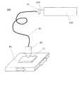
レーザ発振器を用いて加工される電子部品として、例えば、図1に示すような薄膜のチップ抵抗器R1がある。チップ抵抗器R1は、絶縁基板11、上面電極層12、薄膜抵抗体層14、保護膜層16、及び、端面電極層17を備える。絶縁基板11には、例えばアルミナセラミック製の基板等が用いられる。なお、最終形態としてのチップ抵抗器R1の個片化には、絶縁基板11を個別に分割する必要があり、この分割工程を、レーザ光を用いて行うことができる。 As an electronic component processed by using a laser oscillator, for example, there is a thin film chip resistor R1 as shown in FIG. The chip resistor R1 includes an
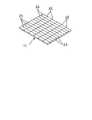
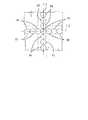
図2のように、個片化される前の絶縁基板11に格子状の分割ラインに沿ってブレイク溝22、23を形成する。次に、絶縁基板11をブレイク溝22、23に沿って「折る」又は「割る」といった操作を行うことにより、個片に分割する。ブレイク溝22、23を形成する際に、レーザが用いられる(以降、この方法をレーザダイシングと称す)。ブレイク溝22、23は、レーザダイシング時に発生するデブリが電極層等に付着することを防ぐために、電極層等を形成する前に、あらかじめ絶縁基板11に形成される。連続したブレイク溝を形成する際に、絶縁基板11がブレイク溝に沿って割れてしまうのを防ぐため、特許文献1では、図3、図4に示すように、複数の比較的浅い第1の穴30と複数の比較的深い第2の穴31とからなるブレイク溝を、ブレイクライン32,33に沿って形成している。特許文献1では、ガルバノミラー式レーザを用い、穴の深さをレーザ光のエネルギーやショット数を変えることにより制御して第1の穴及び第2の穴を形成している。 As shown in FIG. 2,
このような特許文献1の方法では、ガルバノミラーでレーザ光を一定の速度で走査しながら、適宜レーザ発振器のエネルギーを変えたり、ショット数を変えたりする必要がある。しかし、レーザ発振器のエネルギーやパルス数を短時間で切り替えることは難しい。 In such a method of
そこで、特許文献2では、図5に示すように、所定の基本周波数を有する基本波レーザ光と基本周波数の整数倍の周波数を有する1種以上の高調波レーザ光とを同軸上に重畳する方法を用いている。この方法では、レーザ発振器の発振条件を変更することなく、ブレイク溝を形成することができる。 Therefore, in Patent Document 2, as shown in FIG. 5, a method of coaxially superimposing a fundamental wave laser light having a predetermined fundamental frequency and one or more harmonic laser lights having a frequency that is an integral multiple of the fundamental frequency. Is used. In this method, the break groove can be formed without changing the oscillation conditions of the laser oscillator.
しかしながら、特許文献2の装置は、2種類以上のレーザ発振器を有するため、レーザ加工装置が大型になる問題がある。また、異なる波長のレーザ光を、その偏光や波長特性を利用し同軸上に重畳するため、光学系も高価で複雑になり、更に大型化し、光学調整も煩雑になるおそれがある。 However, since the apparatus of Patent Document 2 has two or more types of laser oscillators, there is a problem that the laser processing apparatus becomes large. Further, since laser beams having different wavelengths are superimposed on the same axis by utilizing their polarization and wavelength characteristics, the optical system becomes expensive and complicated, the size is further increased, and the optical adjustment may be complicated.
本開示の目的は、優れた発振効率を有するとともに、小型のレーザ加工装置を実現しうるレーザ発振器及びレーザ加工方法を提供することである。 An object of the present disclosure is to provide a laser oscillator and a laser processing method which have excellent oscillation efficiency and can realize a small-sized laser processing apparatus.
本開示のレーザ発振器は、第1レーザ光を出射する第1レーザダイオードと、前記第1レーザ光とは波長の異なる第2レーザ光を出射する第2レーザダイオードと、前記第1レーザダイオードを駆動する第1電流源と、前記第2レーザダイオードを駆動する第2電流源と、前記第1レーザ光及び前記第2レーザ光を重畳させる合成手段と、前記合成手段によって合成されたレーザ光を外部へ出射する出力鏡と、を備える。 The laser oscillator of the present disclosure drives a first laser diode that emits a first laser beam, a second laser diode that emits a second laser beam having a wavelength different from that of the first laser beam, and the first laser diode. A first current source, a second current source for driving the second laser diode, a synthesizing means for superimposing the first laser beam and the second laser beam, and a laser beam synthesized by the synthesizing means are externally combined. It is equipped with an output mirror that emits light to.
本開示のレーザ加工方法は、前記レーザ発振器を備えるレーザ加工装置を用いたレーザ加工方法であって、前記第1電流源が、前記第1レーザダイオードをパルス波形で発振させることと、前記第2電流源が、前記第2レーザダイオードをパルス波形で発振させることと、を含む。 The laser processing method of the present disclosure is a laser processing method using a laser processing apparatus including the laser oscillator, wherein the first current source oscillates the first laser diode with a pulse waveform, and the second. The current source includes oscillating the second laser diode with a pulse waveform.
本開示のレーザ加工方法は、前記レーザ発振器を備えるレーザ加工装置を用いたレーザ加工方法であって、前記第1電流源が、前記第1レーザダイオードを連続波形で発振させることと、前記第2電流源が、前記第2レーザダイオードをパルス波形で発振させることと、を含む。 The laser processing method of the present disclosure is a laser processing method using a laser processing apparatus including the laser oscillator, wherein the first current source oscillates the first laser diode in a continuous waveform, and the second. The current source includes oscillating the second laser diode with a pulse waveform.
本開示のレーザ発振器及びレーザ加工方法によれば、加工効率を高めることができる。 According to the laser oscillator and the laser processing method of the present disclosure, the processing efficiency can be improved.
本開示のレーザ発振器は、第1レーザダイオードと、第2レーザダイオードと、第1電流源と、第2電流源と、合成手段と、出力鏡と、を備える。第1レーザダイオードは第1レーザ光を出射する。第2レーザダイオードは、第2レーザ光を出射する。第1電流源は、第1レーザダイオードを駆動する。第2電流源は、第2レーザダイオードを駆動する。合成手段は、第1レーザ光及び第2レーザ光を重畳させる。出力鏡は、合成されたレーザ光を外部へ出射する。第1レーザ光の波長と第2レーザ光の波長とは異なる。 The laser oscillator of the present disclosure includes a first laser diode, a second laser diode, a first current source, a second current source, a synthesis means, and an output mirror. The first laser diode emits the first laser beam. The second laser diode emits the second laser beam. The first current source drives the first laser diode. The second current source drives the second laser diode. The synthesizing means superimposes the first laser beam and the second laser beam. The output mirror emits the combined laser beam to the outside. The wavelength of the first laser beam and the wavelength of the second laser beam are different.
本開示のレーザ発振器は、1つのレーザ発振器内に第1電流源と第2電流源を有する。このため、レーザ加工装置は、電流ごとに複数のレーザ発振器を使用しなくてもよい。これにより、小型のレーザ加工装置を実現することができる。また、波長の異なるレーザ光を出射する第1レーザダイオードと第2レーザダイオードとを別の電流源で制御するため、それぞれのレーザダイオードの発振形態、エネルギー量、パワー、及びパルス幅等を効率よく調整することができる。このため、本開示のレーザ発振器を用いたレーザ加工装置では、被加工物の特性及び加工方法に応じてレーザ光を容易に最適化できる。 The laser oscillator of the present disclosure has a first current source and a second current source in one laser oscillator. Therefore, the laser processing apparatus does not have to use a plurality of laser oscillators for each current. As a result, a small laser processing device can be realized. Further, since the first laser diode and the second laser diode that emit laser light having different wavelengths are controlled by different current sources, the oscillation form, energy amount, power, pulse width, etc. of each laser diode are efficiently controlled. Can be adjusted. Therefore, in the laser processing apparatus using the laser oscillator of the present disclosure, the laser beam can be easily optimized according to the characteristics of the workpiece and the processing method.
また、一つの電流源のみで波長の異なるレーザ光を出射する2つのレーザダイオードを制御した場合には、電流ロスが発生する場合がある。例えば、950nm付近の発振波長をもつレーザダイオードと450nm付近の発振波長をもつレーザダイオードとでは、デバイス構造が異なるため、レーザが発振する電流値の閾値が異なる。一つの電源を用いると、最大の電流閾値を持つレーザダイオードに電流源の仕様を合わせる必要がある。しかし、2つ以上の電流源を用いることで、それぞれの発振波長のレーザダイオードに合わせた制御を行うことができ、電流ロスを低減することができる。 Further, when two laser diodes that emit laser light having different wavelengths are controlled by only one current source, a current loss may occur. For example, a laser diode having an oscillation wavelength of about 950 nm and a laser diode having an oscillation wavelength of about 450 nm have different device structures, so that the threshold value of the current value oscillated by the laser is different. With one power source, it is necessary to match the specifications of the current source to the laser diode with the maximum current threshold. However, by using two or more current sources, it is possible to perform control according to the laser diode of each oscillation wavelength, and it is possible to reduce the current loss.
さらに、レーザ加工装置では、レーザダイオード(以下、LDとも称する)を必要に応じでパルス発振させたり、連続(CW)発振させたりするが、パルス発振に比べ、連続(CW)発振の電流源は、発熱量が大きい。このため、連続(CW)発振を行う電流源やレーザダイオードに対して十分な冷却が必要となる。2つ以上の電流源を用いることで、パルス専用とCW専用とで電源を分けて制御できるため、冷却の負荷を抑制することができる。 Further, in the laser processing apparatus, a laser diode (hereinafter, also referred to as LD) is pulse-oscillated or continuously (CW) oscillated as needed, but the current source of continuous (CW) oscillation is higher than that of pulse oscillation. , The amount of heat generated is large. Therefore, sufficient cooling is required for the current source and the laser diode that perform continuous (CW) oscillation. By using two or more current sources, it is possible to control the power supply separately for the pulse dedicated and the CW dedicated, so that the cooling load can be suppressed.
以上のように、本開示のレーザ発振器では、異なる電流源を用いて2つのレーザダイオードを制御しているため、電流ロスを低減することができ、優れた発振効率を実現することができる。したがって、本開示のレーザ発振器を用いたレーザ加工装置は、小型であっても高い加工効率を有することができる。 As described above, in the laser oscillator of the present disclosure, since the two laser diodes are controlled by using different current sources, the current loss can be reduced and excellent oscillation efficiency can be realized. Therefore, the laser processing apparatus using the laser oscillator of the present disclosure can have high processing efficiency even if it is small.
<レーザ発振器>
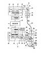
以下、本開示の一実施形態に係るレーザ発振器を、図6及び7を参照して詳細に説明する。本実施形態に係るレーザ発振器130は、第1レーザダイオード(以下、第1LDとも称する)1a〜1bと、第2レーザダイオード(以下、第2LDとも称する)1c〜1eと、第1電流源6と、第2電流源7と、合成手段5と、出力鏡10と、を有する。<Laser oscillator>
Hereinafter, the laser oscillator according to the embodiment of the present disclosure will be described in detail with reference to FIGS. 6 and 7. The
本実施形態に係るレーザ発振器130では、複数のLD1a〜1eから出射される複数のレーザ光が、回折格子などの合成手段5によって重畳され、一本のレーザビームとして集光される。複数のLD1a〜1eから出射されるレーザ光のそれぞれは、合成手段5によって光の伝播方向が変更される。複数のLD1a〜1eのそれぞれは、図6に示すように、離間して配置されているため、合成手段5に入射するレーザ光の入射角がLDごとに異なる。その結果、例えば合成手段5が回折格子である場合、レーザ光の波長が同じであれば、回折格子からの回折強度が極大となる回折角もLDごとに異なる。同様に、例えば合成手段がプリズムである場合、レーザ光の波長が同じであれば、屈折後の透過角もLDごとに異なる。 In the
しかしながら、回折角及び透過角は、レーザ光の波長にも依存する。よって、LDのそれぞれについて、出射されるレーザ光の波長を調整することで、合成手段5からの回折角又は透過角を一定にすることができる。これにより、複数のLD1a〜1eから発するレーザ光は一本のビームにまとめられ、LDの配置に依存せず、特定の方向に集光することができる。その結果、合成手段5によって一本のビームとして集光されたレーザ光は、LDのそれぞれに対応する複数の波長(ロック波長)を有する。 However, the diffraction angle and transmission angle also depend on the wavelength of the laser beam. Therefore, by adjusting the wavelength of the emitted laser light for each of the LDs, the diffraction angle or transmission angle from the synthesis means 5 can be made constant. As a result, the laser light emitted from the plurality of LD1a to 1e can be combined into one beam and focused in a specific direction regardless of the arrangement of the LDs. As a result, the laser beam focused as one beam by the synthesis means 5 has a plurality of wavelengths (lock wavelengths) corresponding to each of the LDs.
図6は、本実施形態に係るレーザ発振器130のレーザ光生成部分を示す概略図である。本実施形態では、DDL方式によるレーザ光生成を用いている。本実施形態では、LD1a〜1eのそれぞれから出射されたレーザ光は、第1コリメータ2a〜2e、回転素子3a〜3e、第2コリメータ4a〜4e、及び合成手段5を介して一本のレーザ光として集光される。集光されたレーザ光は、出力鏡10を介して、外部に向けて出射される。第1コリメータ2a〜2e、回転素子3a〜3e、第2コリメータ4a〜4e、及び、合成手段5が、レーザ光合成部120を構成している。 FIG. 6 is a schematic view showing a laser beam generating portion of the
(レーザダイオード(LD))
LD1a〜1eは、レーザ光を生成し出射する。LDは、例えば、チップ形状のLDチップである。LDチップとしては、端面発光型(EEL:Edge Emitting Laser)のLDチップが好ましく用いられる。端面発光型のLDチップでは、例えば、長尺のバー形状の共振器が、チップ内において基板面と平行に形成されている。共振器の長手方向の一方の端面は光がほぼ全反射するように高反射率の膜で覆われている。一方、共振器の長手方向の他方の端面にも高反射率の膜で覆われているが、反射率は一方の端面に設けられた反射膜よりも小さい。よって、両端面からの反射により増幅され位相の揃ったレーザビームが他方の端面から出射される。共振器の長手方向の長さは、共振器長(CL:Cavity Length)と呼ばれる。(Laser diode (LD))
LD1a to 1e generate and emit laser light. The LD is, for example, a chip-shaped LD chip. As the LD chip, an end face emitting type (EEL: Edge Emitting Laser) LD chip is preferably used. In the end face light emitting type LD chip, for example, a long bar-shaped resonator is formed in the chip in parallel with the substrate surface. One end face in the longitudinal direction of the resonator is covered with a high-reflectance film so that light is almost totally reflected. On the other hand, the other end face in the longitudinal direction of the resonator is also covered with a highly reflective film, but the reflectance is smaller than that of the reflective film provided on one end face. Therefore, the laser beam amplified by the reflection from both end faces and having the same phase is emitted from the other end face. The length of the resonator in the longitudinal direction is called the resonator length (CL: Capacity Length).
LDチップ内に共振器が複数設けられる場合、レーザビームは、他方の端面の複数の箇所から出射され得る。この場合、LDは複数の発光点を有し得る。発光点は、共振器の他方の端面であるチップの端面に沿って、一次元的に整列し得る。 When a plurality of resonators are provided in the LD chip, the laser beam can be emitted from a plurality of locations on the other end face. In this case, the LD may have a plurality of light emitting points. The emission points can be aligned one-dimensionally along the end face of the chip, which is the other end face of the resonator.
上述したように、LD1a〜1eから出射されるレーザ光は、高い出力(利得)が得られる波長帯域にある程度の幅を有する。また、この高出力(利得)が得られる波長帯域は、LDチップの温度に依存して(すなわち、LD1a〜1eを駆動させた期間の長さによって)変化し得る。なお、本実施形態では、LD1a〜1eの駆動開始から十分時間が経過し、LD1a〜1eから発するレーザ光の出力が安定した時点において高出力(利得)が得られる波長帯域内に上述のロック波長が存在するように、LD1a〜1eのそれぞれが構成されている。 As described above, the laser light emitted from the LD1a to 1e has a certain width in the wavelength band in which a high output (gain) can be obtained. Further, the wavelength band in which this high output (gain) is obtained can change depending on the temperature of the LD chip (that is, depending on the length of the period during which the LD1a to 1e are driven). In the present embodiment, the above-mentioned lock wavelength is within the wavelength band in which a high output (gain) can be obtained when a sufficient time has passed from the start of driving the LD1a to 1e and the output of the laser beam emitted from the LD1a to 1e is stable. Each of LD1a to 1e is configured so that
本実施形態では、LD1a〜1bが第1レーザダイオードを構成し、LD1c〜1eが第2レーザダイオードを構成している。すなわち、レーザ発振器130は、2つの第1レーザダイオードと3つの第2レーザダイオードとを有する。しかし、レーザダイオードの個数はこれに限られず、レーザ発振器130は、波長の異なるレーザ光を出射するすくなくとも2つのレーザダイオードを有していればよい。例えば、レーザ発振器130は、1つの第1レーザダイオードと1つの第2レーザダイオードとを有していてもよく、1つの第1レーザダイオードと2つ以上の第2レーザダイオードとを有していてもよく、2つ以上の第1レーザダイオードと1つの第2レーザダイオードとを有していてもよく、2つ以上の第1レーザダイオードと2つ以上の第2レーザダイオードとを有していてもよい。LDの個数は、所望のレーザ出力に応じて調整すればよい。 In the present embodiment, LD1a to 1b constitute a first laser diode, and LD1c to 1e constitute a second laser diode. That is, the
レーザ発振器130が、複数の第1レーザダイオードを有する場合、複数の第1レーザダイオードから出射される複数の第1レーザ光の波長の平均波長をλ1としたときに、複数の第1レーザ光の各々の波長は、λ1±50nmの範囲内であることが好ましい。すなわち、本実施形態では、LD1a〜1bのそれぞれから出射されるレーザ光の平均波長をλ1としたときに、LD1a〜1bのそれぞれから出射されるレーザ光の波長は、λ1±50nmの範囲内であることが好ましい。この場合、レーザ発振器130が複数の第1レーザダイオードを有していても、第1電流源6を用いて効率よくLDの発振を制御することが出来る。When the
レーザ発振器130が、複数の第2レーザダイオードを有する場合、複数の第2レーザダイオードから出射される複数の第2レーザ光の波長の平均波長をλ2としたときに、複数の第2レーザ光の各々の波長は、λ2±50nmの範囲内であることが好ましい。すなわち、本実施形態では、LD1c〜1eのそれぞれから出射されるレーザ光の平均波長をλ2としたときに、LD1c〜1eのそれぞれから出射されるレーザ光の波長は、λ2±50nmの範囲内であることが好ましい。この場合、レーザ発振器130が複数の第2レーザダイオードを有していても、第2電流源7を用いて効率よくLDの発振を制御することが出来る。When the
第1レーザ光及び第2レーザ光の波長は特に限定されず、例えば、ピーク波長が975±25nm又は895±25nmである赤外レーザ、又は、ピーク波長が400〜450nmである青色レーザなどを用いることができる。 The wavelengths of the first laser beam and the second laser beam are not particularly limited, and for example, an infrared laser having a peak wavelength of 975 ± 25 nm or 895 ± 25 nm, a blue laser having a peak wavelength of 400 to 450 nm, or the like is used. be able to.
例えば、第1レーザ光の波長は、380nm以上500nm以下の範囲内であってよい。また、例えば、第2レーザ光の波長は、700nm以上1100nm以下の範囲内であってよい。このように、第1レーザ光の波長と第2レーザ光の波長とが異なることで、被加工物の物性に応じて最適な加工を行うことができる。赤色のレーザ光と比較して青色のレーザ光を、約6倍の吸収率で吸収する銅等の材料の場合、加工の初期段階において青色レーザビームを用いて材料を溶融させ、その後、赤色レーザビームの吸収率が増大したところで、赤色レーザビームで高出力の照射を行うことができる。この場合、材料に対して、過剰なパワーやエネルギーの入力を抑え、精度の高い加工が実現できる。 For example, the wavelength of the first laser beam may be in the range of 380 nm or more and 500 nm or less. Further, for example, the wavelength of the second laser beam may be in the range of 700 nm or more and 1100 nm or less. As described above, since the wavelength of the first laser beam and the wavelength of the second laser beam are different, optimum processing can be performed according to the physical properties of the workpiece. In the case of a material such as copper that absorbs blue laser light at about 6 times the absorption rate compared to red laser light, the material is melted using a blue laser beam in the initial stage of processing, and then the red laser is used. When the absorption rate of the beam is increased, high-power irradiation can be performed with the red laser beam. In this case, it is possible to suppress an excessive input of power or energy to the material and realize highly accurate processing.
レーザ発振器130は、第1レーザダイオード及び第2レーザダイオード以外のレーザダイオードを有していてもよい。例えば、レーザ発振器130は、第1レーザ光及び第2レーザ光と波長の異なる第3レーザ光を出射する第3レーザダイオードを有してもよい。この場合でも、第3レーザダイオードを、第1電流源及び第2電流源と異なる第3電流源で駆動させることで、電流ロスが少なく優れた発振効率を有するレーザ発振器を得ることができる。なお、レーザ発振器130が、第3レーザダイオードを有する場合、第3レーザダイオードの個数は1つであってもよく、2つ以上であってもよい。 The
(電流源)
レーザ発振器130は、図7に示すように、第1レーザダイオード1a〜1bを駆動する第1電流源6と、第2レーザダイオード1c〜1eを駆動する第2電流源7と、を有する。本実施形態では、図7に示すように、LD1a〜1eは電流源6,7に直列で接続されているが、並列で接続されていてもよい。(Current source)
As shown in FIG. 7, the
本実施形態では、第1レーザダイオード1a〜1bが第1電流源6に接続されているが、第1レーザダイオード1a〜1bがそれぞれ別の第1電流源6に接続されていてもよい。すなわち、レーザ発振器130が2つの第1電流源6を有し、一つの第1電流源6に第1レーザダイオード1aが接続され、他方の第1電流源6に第1レーザダイオード1bが接続されていてもよい。 In the present embodiment, the first laser diodes 1a to 1b are connected to the first
本実施形態では、第2レーザダイオード1c〜1eが第2電流源7に接続されているが、第2レーザダイオード1c〜1eがそれぞれ別の第2電流源7に接続されていてもよい。すなわち、レーザ発振器130が3つの第2電流源7を有し、それぞれが第2レーザダイオード1c〜1eのうちの一つに接続されていてもよい。もちろん、レーザ発振器130が2つの第2電流源7を有し、一方の第2電流源7が第2レーザダイオード1c〜1eのうちの二つに接続され、他方の第2電流源7が第2レーザダイオード1c〜1eのうちの残りの一つに接続されていてもよい。 In the present embodiment, the
第1電流源6は、第1レーザダイオード1a〜1bをパルス波形及び連続波形の少なくとも一方で発振させる。すなわち、第1電流源6は、第1レーザダイオード1a〜1bをパルス発振する制御を行ってもよく、連続発振する制御を行ってもよく、パルス発振及び連続発振の両方の制御を行ってもよい。パルス発振とは、第1レーザダイオード1a〜1bがレーザ光を連続的に発振するのではなく、短時間の発振を断続的に繰り返すことを意味する。連続発振とは、第1レーザダイオード1a〜1bがレーザ光を連続的に発振することを意味する。 The first
第2電流源7は、第2レーザダイオード1c〜1eをパルス波形及び連続波形の少なくとも一方で発振させる。すなわち、第2電流源7は、第2レーザダイオード1c〜1eをパルス発振する制御を行ってもよく、連続発振する制御を行ってもよく、パルス発振及び連続発振の両方の制御を行ってもよい。 The second
(第1コリメータ)
本実施形態では、LD1a〜1eから出射される光は、第1コリメータ2a〜2eによってそれぞれ整形されている。LD1a〜1eのそれぞれから出射されるレーザ光は、伝播に伴い拡散し、ビーム幅が広がる。第1コリメータ2a〜2eは、LD1a〜1eから出射されるレーザ光を第1方向に平行光化する。すなわち、第1コリメータ2a〜2eは、LD1a〜1eから出射されるレーザ光の第1方向におけるビーム幅を縮小し、レーザ光を平行光化する。これにより、第1方向におけるビーム幅が狭められる。なお、第1方向とは、ビーム幅の広がりが最も大きくなる方向を意味する。すなわち、第1方向とは、LDチップの基板面に垂直な方向である。LDチップの基板面に垂直な方向は、一般に、LDチップから発するレーザ光の速軸の方向であり得る。これに対し、LDチップの基板面に平行で且つ光の出射面に沿う方向は、一般に、LDチップから出射されるレーザ光の遅軸の方向であり得る。第1コリメータ2a〜2eの種類は特に限定されず、例えば凸レンズであってよい。(1st collimator)
In the present embodiment, the light emitted from the LD1a to 1e is shaped by the
なお、本実施形態では、レーザ発振器130が第1コリメータ2a〜2eを有する態様であるが、これに限られず、レーザ発振器130は第1コリメータ2a〜2eを有していなくてもよい。また、レーザ発振器130中のLDのいくつかのみに対応する第1コリメータ2a〜2eを有していてもよい。 In the present embodiment, the
(回転素子)
本実施形態では、LD1a〜1eから出射される光は、回転素子3a〜3eによってそれぞれ回転させられる。すなわち、回転素子3a〜3eは、第1コリメータ2a〜2eによって整形されたレーザ光を回転させる。なお、光を回転させる、とは、光(ビーム)の伝播方向に垂直な面における断面形状を回転させることを意味する。(Rotating element)
In the present embodiment, the light emitted from the LD1a to 1e is rotated by the
LD1a〜1eが複数の発光点を有するLDチップである場合、発光点に対応する複数のレーザ光が生成及び出射され、伝播に伴い拡散し、ビーム幅が広がる。このとき、回転素子3a〜3eは、発光点の異なるレーザ光のビーム同士の重なりが低減されるように、それぞれのレーザビームの断面形状を回転させる。これにより、高出力のレーザビームが得られる。 When the LD1a to 1e are LD chips having a plurality of light emitting points, a plurality of laser beams corresponding to the light emitting points are generated and emitted, diffused with propagation, and the beam width is widened. At this time, the
回転素子3a〜3eを通過する前において、発光点の異なる複数のレーザ光のビーム断面は、LDチップの基板面に平行で且つ光の出射面(チップ端面)に沿う方向に整列している。また、第1コリメータ2a〜2eによる平行光化を受けているので、それぞれのレーザ光のビーム形状は、第1方向を短軸とする扁平な形状(例えば、楕円又は方形)となっている。回転素子3a〜3eは、例えば、楕円形状のビームの長軸方向と基板面とのなす角が直角に近づくように(すなわち、短軸方向と基板面とのなす角が0°に近づくように)、楕円形状のビームを回転させる。例えば、第1方向がLDチップの基板面に垂直な方向である場合、レーザ光は回転素子3a〜3eによって90°回転され得る。回転素子3a〜3eの種類は特に限定されず、例えば凸レンズであってよい。回転素子3a〜3eは、レーザ光の出射方向に垂直であって且つ基板面に対し例えば45°傾いた軸を有する円柱レンズを発光点の整列方向に沿って配列させることで設けることができる。 Before passing through the
第1コリメータ2a〜2e及び回転素子3a〜3eは、それぞれ、対応するLD1a〜1eに取り付けられていてよい。すなわち、LD1a〜1eと、対応する第1コリメータ2a〜2eと、対応する回転素子3a〜3eとが一体化された部品を用いてもよい。 The
なお、本実施形態では、レーザ発振器130が回転素子3a〜3eを有する態様であるが、これに限られず、レーザ発振器130は回転素子を有していなくてもよい。また、レーザ発振器130中のLDのいくつかのみに対応する回転素子を有していてもよい。 In the present embodiment, the
(第2コリメータ)
本実施形態では、LD1a〜1eから出射される光は、第2コリメータ4a〜4eによってそれぞれ整形されている。第2コリメータ4a〜4eは、第1コリメータ2a〜2eによって整形され、回転素子3a〜3eによって回転された光を、第2方向において平行化する。すなわち、第2コリメータ4a〜4eは、レーザ光の第2方向におけるビーム幅を縮小し、レーザ光を平行光化する。これにより、第2方向におけるビーム幅が狭められる。回転素子3a〜3eを設けない場合、第2方向は、第1方向と異なる方向、例えば第1方向に垂直な方向である。回転素子3a〜3eが設けられる場合、第2方向は、回転後の第1方向と異なる方向、例えば回転後の第1方向に垂直な方向である。回転素子3a〜3eがレーザ光を90°回転させる場合、第1方向と第2方向とは平行であり得る。第2方向は、LDチップから発するレーザ光の遅軸の方向であり得る。第2コリメータ4a〜4eの種類は特に限定されず、例えば凸レンズであってよい。(2nd collimator)
In the present embodiment, the light emitted from the LD1a to 1e is shaped by the
なお、本実施形態では、レーザ発振器130が第2コリメータ4a〜4eを有する態様であるが、これに限られず、レーザ発振器130は第2コリメータを有していなくてもよい。また、レーザ発振器130中のLDのいくつかのみに対応する第2コリメータを有していてもよい。 In the present embodiment, the
(合成手段)
レーザ発振器130は、第1レーザ光及び第2レーザ光を重畳させる合成手段5を有する。本実施形態では、合成手段5は、回折格子であり、LD1a〜1eから出射され、第1コリメータ2a〜2e、回転素子3a〜3e、及び第2コリメータ4a〜4eを通過したレーザ光を、特定の方向に向けて集光する。回折格子は、反射型であってもよく、透過型であってもよい。(Synthesis means)
The
LD1a〜1eは、レーザ発振器130内で互いに離間して配置される。このため、回折格子に入射されるレーザ光の入射角がLD1a〜1eごとに異なる。一般に、回折強度が極大となる回折角は入射角に依存するので、LDから出射されるレーザ光の波長を同じとすれば、回折角もLDごとに異なり、同一方向への集光が難しい。 The LD1a to 1e are arranged apart from each other in the
しかしながら、回折角は波長にも依存するため、LD1a〜1eが出射するレーザ光の波長を互いに異ならせておくことで、回折格子への入射角がLD1a〜1eごとに異なる場合であっても、回折角を一定とし、LD1a〜1eから出射されたレーザ光を特定の方向に集光することができる。この特定の方向に、LD1a〜1eのそれぞれから出射されたレーザ光が回折するときの波長をロック波長と呼ぶ。ロック波長は、LD1a〜1eごとに異なる。 However, since the diffraction angle also depends on the wavelength, by making the wavelengths of the laser beams emitted by the LD1a to 1e different from each other, even if the angle of incidence on the diffraction grating is different for each of the LD1a to 1e. The diffraction angle is constant, and the laser light emitted from the LD1a to 1e can be focused in a specific direction. The wavelength at which the laser light emitted from each of the LD1a to 1e is diffracted in this specific direction is called a lock wavelength. The lock wavelength is different for each of LD1a to 1e.
よって、回折格子により集光されたレーザ光は、LD1a〜1eごとに異なる複数の波長(ロック波長)を有する。すなわち、回折格子により集光されたレーザ光には、それぞれが異なるロック波長をピークに持つ波長分布を有する複数のレーザ光が重畳されている。 Therefore, the laser light focused by the diffraction grating has a plurality of different wavelengths (lock wavelengths) for each of the LD1a to 1e. That is, a plurality of laser beams having a wavelength distribution having different lock wavelengths as peaks are superimposed on the laser light focused by the diffraction grating.
なお、合成手段5は回折格子に限定されず、波長の違いを用いた合成手段、偏光特性を用いた合成手段、及び空間合成手段を用いればよい。波長の違いを用いた合成手段では、例えば、ダイクロックミラーやプリズムを用いて波長の異なるレーザ光を結合することができる。レーザ光の偏光特性を用いた合成手段では、例えば、一つのレーザ光の偏光方向と他のレーザ光の偏光方向とのなす角が90度となるようにし、偏光ビームスプリッターを用いてレーザ光を結合することができる。空間合成手段では、例えば、集光レンズやミラーを用いて空間的にレーザ光を結合することができる。 The synthesis means 5 is not limited to the diffraction grating, and a synthesis means using a difference in wavelength, a synthesis means using polarization characteristics, and a spatial synthesis means may be used. In the synthesis means using different wavelengths, for example, a dichroic mirror or a prism can be used to combine laser beams having different wavelengths. In the synthesis means using the polarization characteristics of the laser beam, for example, the angle between the polarization direction of one laser beam and the polarization direction of the other laser beam is set to 90 degrees, and the laser beam is split by using a polarizing beam splitter. Can be combined. In the spatial synthesis means, for example, the laser beam can be spatially coupled by using a condenser lens or a mirror.
(出力鏡)
出力鏡10は、合成手段に5によって重畳され集光されたレーザ光を、その一部を除いて反射させ、LD1a〜1e側に戻す。これにより、レーザ発振器130内において、レーザ光を外部共振させる。外部共振により出力が高められたレーザ光の一部は、出力鏡10を透過し、外部に出射される。(Output mirror)
The
<レーザ加工装置>
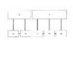
図8は、本開示のレーザ発振器130を用いたレーザ加工装置200を示す概略図である。レーザ発振器130から射出された射出レーザ光140は、入射集光光学系81により集光され、伝送用光ファイバー82に導入される。さらに伝送用光ファイバー82により、射出集光光学系83まで導かれ、集光されたレーザ光が被加工物である絶縁基板11に照射される。絶縁基板11はXY移動テーブル84により一定速度で走査され、加工が行われる。<Laser processing equipment>
FIG. 8 is a schematic view showing a
なお、本実施形態では、被加工物として絶縁基板11を用いているが、これに限定されず、レーザ加工装置200によって加工可能な被加工物の加工を行うことができる。 In the present embodiment, the insulating
<レーザ加工方法>
本開示のレーザ発振器130を備えるレーザ加工装置200を用いたレーザ加工方法について、説明する。<Laser processing method>
A laser processing method using a
(レーザ加工方法の第一実施形態)
図9〜図11を用いて、本開示の第一実施形態に係るレーザ加工方法を説明する。図9は、レーザ発振器130の制御方法において、LD1a〜1eを駆動させる電流源6,7の駆動方法を示す。電流源6、7にパルス駆動の電流が印加されることにより、LD1a〜1eは、パルス化されたレーザ光を発振する。91のパルス波形、92のパルス波形は、それぞれ電流源6,7に印加される電流のパルス波形を表す。印加される電流値に応じて、LD1a〜1eから発振されるレーザ光の出力を変えることができる。また、発振されるパルスの経過時間をパルス幅(μs)、隣り合うパルスの間隔を周期(μs)と呼ぶ。(First Embodiment of Laser Machining Method)
The laser processing method according to the first embodiment of the present disclosure will be described with reference to FIGS. 9 to 11. FIG. 9 shows a method of driving the
図9において、第1電流源6に印加される電流値をA1(A)としたときのLD1a、LD1bから発振されるレーザ出力をW1(W)、パルス幅t1(μs)とすると、LD1a、LD1bから発振されるレーザのエネルギーE1は、E1=W1/t1(J)となる。同様に第2電流源7に印加される電流値をA2(A)としたときのLD1c〜LD1eから発振されるレーザ出力をW2(W)、パルス幅t2(μs)とすると、LD1c〜LD1eから発振されるレーザのエネルギーE2は、E2=W2/t2(J)となる。なお、第1電流源6には2個のLD、第2電流源7には3個のLDが接続されているので、第1電流源6に接続されたLDから発振されるレーザエネルギーはE1×2(J)、電源流7に接続されたLDから発振されるレーザエネルギーは、E2×3(J)となる。 In FIG. 9, when the laser output oscillated from LD1a and LD1b is W1 (W) and the pulse width is t1 (μs) when the current value applied to the first
図10及び11は、図8のレーザ加工装置200により、図9の制御方法で絶縁基板11にレーザ光を照射し、第1の穴30及び第2の穴31を形成した絶縁基板11の断面図及び平面図をそれぞれ示す。第1の穴30は、第1電流源6により駆動されたLD1a〜1bから発振されたレーザ光で加工された穴であり、第2の穴31は、第2電流源7により駆動されたLD1c〜1eから発振されたレーザ光で加工された穴である。 10 and 11 show a cross section of the insulating
第2電流源7により駆動されたLD1c〜1eから発振されたレーザ光のエネルギーは、第1電流源6により駆動されたLD1a〜1bから発振されたレーザ光のエネルギーが大きい。よって、図10に示されるように、第2の穴31の加工深さf2は、第1の穴30の加工深さf1より深くなる。また、図11に示されるように、第2の穴31の加工径d2は、第1の穴30の加工径d1より大きくなる。 The energy of the laser beam oscillated from the LD1c to 1e driven by the second
また、第1の穴30間のピッチp1(図10参照)は、第1電流源6のパルス周期をT(μs)、絶縁基板11の搬送速度をV(mm/s)としたとき、p1=V×Tで表すことができる。 Further, the pitch p1 (see FIG. 10) between the
(レーザ加工方法の第二実施形態)
図12〜14を用いて、本開示の第二実施形態に係るレーザ加工方法を説明する。図12は、レーザ発振器130の制御方法において、LD1a〜1eを駆動させる電流源6,7の駆動方法を示す。第1電流源6に連続駆動の電流が印加されることにより、LD1a〜1bは、レーザを連続発振する。一方、第2電流源7にはパルス駆動の電流が印加され、LD1c〜1eはパルス化されたレーザ光を発振する。93の連続波形、92のパルス波形は、それぞれ電流源6,7に印加される電流の波形を表す。印加される電流値に応じて、LD1a〜1eから発振されるレーザの出力を変えることができる。また、発振されるパルスの経過時間をパルス幅(μs)、隣り合うパルスの間隔を周期(μs)と呼ぶ。(Second Embodiment of Laser Machining Method)
The laser processing method according to the second embodiment of the present disclosure will be described with reference to FIGS. 12 to 14. FIG. 12 shows a method of driving the
図12において、第1電流源6に印加される電流値を一定のA1(A)としたとき、LD1a、LD1bから発振されるレーザ光は連続光(CW)で発振される。第1電流源6に接続されたLD1a〜1bから発振されるレーザ出力はW1×2(W)、電源流7に接続されたLD1c〜1eから発振されるレーザエネルギーは、E2×3(J)になる。 In FIG. 12, when the current value applied to the first
図13及び14は、図8のレーザ加工装置200により、図12の制御方法で絶縁基板11にレーザ光を照射し、第1の加工溝131及び第2の穴31を形成した絶縁基板11の断面図及び平面図をそれぞれ示す。第1の加工溝131は、第1電流源6により駆動されたLD1a〜1bから発振されたレーザ光で加工された溝であり、第2の穴31は、第2電流源7により駆動されたLD1c〜1eから発振されたレーザ光で加工された穴である。 13 and 14 show the insulating
第1電流源6により駆動されたLD1a〜1bから発振されたレーザ光により形成された第1の加工溝131の溝深さはf3であり(図13参照)、溝幅はs1である(図14参照)。 The groove depth of the first
なお、LD1a〜1bは、パルス化されたレーザを発振し、LD1c〜1eは、レーザを連続発振してもよいことは言うまでもない。また、LD1a〜1bと、LD1c〜1eの両方が、レーザを連続発振してもよいことは言うまでもない。 Needless to say, LD1a to 1b may oscillate a pulsed laser, and LD1c to 1e may oscillate a laser continuously. Needless to say, both LD1a to 1b and LD1c to 1e may continuously oscillate the laser.
本開示のレーザ発振器及びレーザ加工方法は、電子部品の製造方法、特に絶縁基板を切断によって分割して複数の電子部品を取り出す工程において有用である。 The laser oscillator and the laser processing method of the present disclosure are useful in a method for manufacturing an electronic component, particularly in a step of dividing an insulating substrate by cutting to take out a plurality of electronic components.
11 絶縁基板
12 上面電極層
14 薄膜抵抗体層
16 保護膜層
17 端面電極層
22、23 ブレイク溝
30 第1の穴
31 第2の穴
32、33 ブレイクライン
1a〜1b 第1レーザダイオード
1c〜1e 第2レーザダイオード
2a〜2e 第1コリメータ
3a〜3e 回転素子
4a〜4e 第2コリメータ
5 合成手段
6 第1電流源
7 第2電流源
10 出力鏡
120 レーザ光合成部
130 レーザ発振器
140 射出レーザ光
81 入射集光光学系
82 伝送用光ファイバー
83 射出集光光学系
84 XY移動テーブル
91 第1電流源のパルス波形
92 第2電流源のパルス波形
93 第1電流源の連続(CW)波形
131 第1の加工溝
200 レーザ加工装置
11
Claims (9)
Translated fromJapanese前記第1レーザ光とは波長の異なる第2レーザ光を出射する第2レーザダイオードと、
前記第1レーザダイオードを駆動する第1電流源と、
前記第2レーザダイオードを駆動する第2電流源と、
前記第1レーザ光及び前記第2レーザ光を重畳させる合成手段と、
前記合成手段によって合成されたレーザ光を外部へ出射する出力鏡と、を備える、レーザ発振器。The first laser diode that emits the first laser beam and
A second laser diode that emits a second laser beam having a wavelength different from that of the first laser beam,
The first current source that drives the first laser diode and
The second current source that drives the second laser diode and
A synthesis means for superimposing the first laser beam and the second laser beam, and
A laser oscillator including an output mirror that emits a laser beam synthesized by the synthesis means to the outside.
請求項1に記載のレーザ発振器。The first current source causes the first laser diode to oscillate at least one of a pulse waveform and a continuous waveform.
The laser oscillator according to claim 1.
請求項1又は2に記載のレーザ発振器。The second current source causes the second laser diode to oscillate at least one of a pulsed waveform and a continuous waveform.
The laser oscillator according to claim 1 or 2.
複数の前記第1レーザダイオードから出射される複数の前記第1レーザ光の波長の平均波長をλ1としたときに、複数の前記第1レーザ光の各々の波長は、λ1±50nmの範囲内である、
請求項1から3のいずれか1項に記載のレーザ発振器。The laser oscillator includes a plurality of the first laser diodes.
When the average wavelength of the wavelengths of the plurality of first laser beams emitted from the plurality of first laser diodes is λ1 , each wavelength of the plurality of first laser beams is inthe range of λ 1 ± 50 nm. Inside,
The laser oscillator according to any one of claims 1 to 3.
請求項4に記載のレーザ発振器。The average wavelength λ1 is in the range of 380 nm or more and 500 nm or less.
The laser oscillator according to claim 4.
複数の前記第2レーザダイオードから出射される複数の前記第2レーザ光の波長の平均波長をλ2としたときに、複数の前記第2レーザ光の各々の波長は、λ2±50nmの範囲内である、
請求項1から5のいずれか1項に記載のレーザ発振器。The laser oscillator includes a plurality of the second laser diodes.
When the average wavelength of the wavelengths of the plurality of second laser beams emitted from the plurality of second laser diodes is λ2 , each wavelength of the plurality of second laser beams is inthe range of λ 2 ± 50 nm. Inside,
The laser oscillator according to any one of claims 1 to 5.
請求項6に記載のレーザ発振器。The average wavelength λ2 is in the range of 700 nm or more and 1100 nm or less.
The laser oscillator according to claim 6.
前記第1電流源が、前記第1レーザダイオードをパルス波形で発振させることと、
前記第2電流源が、前記第2レーザダイオードをパルス波形で発振させることと、を含む
レーザ加工方法。A laser processing method using a laser processing apparatus including the laser oscillator according to any one of claims 1 to 7.
The first current source causes the first laser diode to oscillate in a pulse waveform.
A laser processing method comprising a method in which the second current source oscillates the second laser diode in a pulse waveform.
前記第1電流源が、前記第1レーザダイオードを連続波形で発振させることと、
前記第2電流源が、前記第2レーザダイオードをパルス波形で発振させることと、を含む
レーザ加工方法。
A laser processing method using a laser processing apparatus including the laser oscillator according to any one of claims 1 to 7.
The first current source causes the first laser diode to oscillate in a continuous waveform.
A laser processing method comprising a method in which the second current source oscillates the second laser diode in a pulse waveform.
Priority Applications (3)
| Application Number | Priority Date | Filing Date | Title |
|---|---|---|---|
| JP2020010979AJP2021118271A (en) | 2020-01-27 | 2020-01-27 | Laser oscillator and laser machining method |
| US17/092,841US20210234337A1 (en) | 2020-01-27 | 2020-11-09 | Laser oscillator and laser processing method |
| CN202011643944.2ACN113258433A (en) | 2020-01-27 | 2020-12-31 | Laser oscillator and laser processing method |
Applications Claiming Priority (1)
| Application Number | Priority Date | Filing Date | Title |
|---|---|---|---|
| JP2020010979AJP2021118271A (en) | 2020-01-27 | 2020-01-27 | Laser oscillator and laser machining method |
Publications (1)
| Publication Number | Publication Date |
|---|---|
| JP2021118271Atrue JP2021118271A (en) | 2021-08-10 |
Family
ID=76970907
Family Applications (1)
| Application Number | Title | Priority Date | Filing Date |
|---|---|---|---|
| JP2020010979APendingJP2021118271A (en) | 2020-01-27 | 2020-01-27 | Laser oscillator and laser machining method |
Country Status (3)
| Country | Link |
|---|---|
| US (1) | US20210234337A1 (en) |
| JP (1) | JP2021118271A (en) |
| CN (1) | CN113258433A (en) |
Families Citing this family (2)
| Publication number | Priority date | Publication date | Assignee | Title |
|---|---|---|---|---|
| WO2021044730A1 (en)* | 2019-09-06 | 2021-03-11 | パナソニックIpマネジメント株式会社 | Laser oscillation device |
| GB2623803A (en)* | 2022-10-27 | 2024-05-01 | Bright Beams Laser Tech Ltd | Optical system |
Citations (4)
| Publication number | Priority date | Publication date | Assignee | Title |
|---|---|---|---|---|
| US20070002925A1 (en)* | 2004-10-25 | 2007-01-04 | Nuvonyx, Inc. | External cavity laser diode system and method thereof |
| WO2017122611A1 (en)* | 2016-01-14 | 2017-07-20 | 株式会社アマダミヤチ | Laser device |
| JP2018034184A (en)* | 2016-08-31 | 2018-03-08 | パナソニックIpマネジメント株式会社 | Laser oscillator and laser processing apparatus |
| WO2020017214A1 (en)* | 2018-07-20 | 2020-01-23 | パナソニック株式会社 | Light-emitting device, optical device, and wavelength combining method |
Family Cites Families (14)
| Publication number | Priority date | Publication date | Assignee | Title |
|---|---|---|---|---|
| US5745153A (en)* | 1992-12-07 | 1998-04-28 | Eastman Kodak Company | Optical means for using diode laser arrays in laser multibeam printers and recorders |
| JP4083464B2 (en)* | 2002-05-02 | 2008-04-30 | 富士通株式会社 | Wavelength tunable light source device and optical amplifier using the same |
| US8804246B2 (en)* | 2008-05-08 | 2014-08-12 | Ii-Vi Laser Enterprise Gmbh | High brightness diode output methods and devices |
| US9093822B1 (en)* | 2010-12-20 | 2015-07-28 | TeraDiode, Inc. | Multi-band co-bore-sighted scalable output power laser system |
| US9620933B1 (en)* | 2013-04-06 | 2017-04-11 | TeraDiode, Inc. | High brightness, monolithic, multispectral semiconductor laser |
| CN107005020B (en)* | 2014-10-15 | 2021-07-20 | 朗美通经营有限责任公司 | Laser system and method of tuning the output power of a laser system |
| JP2016181643A (en)* | 2015-03-25 | 2016-10-13 | 株式会社アマダホールディングス | Semiconductor laser oscillator |
| WO2017106192A1 (en)* | 2015-12-16 | 2017-06-22 | Coherent, Inc. | Stackable electrically-isolated diode-laser bar assembly |
| US10444610B2 (en)* | 2017-07-27 | 2019-10-15 | North Inc. | Systems, devices, and methods for laser projectors |
| US10222474B1 (en)* | 2017-12-13 | 2019-03-05 | Soraa Laser Diode, Inc. | Lidar systems including a gallium and nitrogen containing laser light source |
| US11070032B2 (en)* | 2018-01-09 | 2021-07-20 | Daylight Solutions, Inc. | Laser assembly with spectral beam combining |
| US10559943B2 (en)* | 2018-01-09 | 2020-02-11 | Daylight Solutions, Inc. | Laser assembly with spectral beam combining |
| JP7280498B2 (en)* | 2019-06-10 | 2023-05-24 | 日亜化学工業株式会社 | Light source device |
| WO2021044730A1 (en)* | 2019-09-06 | 2021-03-11 | パナソニックIpマネジメント株式会社 | Laser oscillation device |
- 2020
- 2020-01-27JPJP2020010979Apatent/JP2021118271A/enactivePending
- 2020-11-09USUS17/092,841patent/US20210234337A1/ennot_activeAbandoned
- 2020-12-31CNCN202011643944.2Apatent/CN113258433A/enactivePending
Patent Citations (4)
| Publication number | Priority date | Publication date | Assignee | Title |
|---|---|---|---|---|
| US20070002925A1 (en)* | 2004-10-25 | 2007-01-04 | Nuvonyx, Inc. | External cavity laser diode system and method thereof |
| WO2017122611A1 (en)* | 2016-01-14 | 2017-07-20 | 株式会社アマダミヤチ | Laser device |
| JP2018034184A (en)* | 2016-08-31 | 2018-03-08 | パナソニックIpマネジメント株式会社 | Laser oscillator and laser processing apparatus |
| WO2020017214A1 (en)* | 2018-07-20 | 2020-01-23 | パナソニック株式会社 | Light-emitting device, optical device, and wavelength combining method |
Also Published As
| Publication number | Publication date |
|---|---|
| CN113258433A (en) | 2021-08-13 |
| US20210234337A1 (en) | 2021-07-29 |
Similar Documents
| Publication | Publication Date | Title |
|---|---|---|
| US7602822B2 (en) | Fiber laser based production of laser drilled microvias for multi-layer drilling, dicing, trimming of milling applications | |
| US6331692B1 (en) | Diode laser, laser optics, device for laser treatment of a workpiece, process for a laser treatment of workpiece | |
| JP6261471B2 (en) | Laser processing equipment | |
| US20180026425A1 (en) | Semiconductor laser oscillator | |
| WO2016060103A1 (en) | Semiconductor laser oscillator | |
| JPWO2020166420A1 (en) | Laser processing machine, processing method and laser light source | |
| US20220072662A1 (en) | Laser processing device and laser processing method using same | |
| JP5536319B2 (en) | Laser scribing method and apparatus | |
| JP6385622B1 (en) | Laser processing method and laser processing apparatus | |
| JP2016112609A (en) | Laser cutting apparatus and laser cutting method | |
| JP5391077B2 (en) | Laser beam irradiation device | |
| JP2021118271A (en) | Laser oscillator and laser machining method | |
| JP6522166B2 (en) | Laser device | |
| US6255619B1 (en) | Lens, semiconductor laser element, device for machining the lens and element, process for producing semiconductor laser element, optical element, and device and method for machining optical element | |
| JP6261472B2 (en) | Laser processing equipment | |
| JP2016073983A (en) | Laser welding device and laser welding method | |
| JP2000343254A (en) | Laser line patterning method | |
| US20220173576A1 (en) | Laser oscillation device | |
| JP7422355B2 (en) | laser oscillator | |
| JP7319664B2 (en) | LASER PROCESSING APPARATUS AND LASER PROCESSING METHOD | |
| JP3494517B2 (en) | Solid state laser device | |
| JP7384349B2 (en) | Laser irradiation method and laser irradiation device | |
| JP2005284033A (en) | Beam shaping device, laser oscillation device, and laser machining device | |
| JP2025036912A (en) | Laser module, and laser device and laser processing device equipped with the same | |
| KR101098259B1 (en) | Laser scribe method and apparatus |
Legal Events
| Date | Code | Title | Description |
|---|---|---|---|
| A621 | Written request for application examination | Free format text:JAPANESE INTERMEDIATE CODE: A621 Effective date:20221118 | |
| A977 | Report on retrieval | Free format text:JAPANESE INTERMEDIATE CODE: A971007 Effective date:20230830 | |
| A131 | Notification of reasons for refusal | Free format text:JAPANESE INTERMEDIATE CODE: A131 Effective date:20230905 | |
| A02 | Decision of refusal | Free format text:JAPANESE INTERMEDIATE CODE: A02 Effective date:20240305 |