JP2021118234A - Semiconductor storage device - Google Patents
Semiconductor storage deviceDownload PDFInfo
- Publication number
- JP2021118234A JP2021118234AJP2020009505AJP2020009505AJP2021118234AJP 2021118234 AJP2021118234 AJP 2021118234AJP 2020009505 AJP2020009505 AJP 2020009505AJP 2020009505 AJP2020009505 AJP 2020009505AJP 2021118234 AJP2021118234 AJP 2021118234A
- Authority
- JP
- Japan
- Prior art keywords
- conductive layer
- layer
- thickness
- insulating
- conductive
- Prior art date
- Legal status (The legal status is an assumption and is not a legal conclusion. Google has not performed a legal analysis and makes no representation as to the accuracy of the status listed.)
- Pending
Links
Images


Classifications
- H—ELECTRICITY
- H01—ELECTRIC ELEMENTS
- H01L—SEMICONDUCTOR DEVICES NOT COVERED BY CLASS H10
- H01L25/00—Assemblies consisting of a plurality of semiconductor or other solid state devices
- H01L25/03—Assemblies consisting of a plurality of semiconductor or other solid state devices all the devices being of a type provided for in a single subclass of subclasses H10B, H10D, H10F, H10H, H10K or H10N, e.g. assemblies of rectifier diodes
- H01L25/04—Assemblies consisting of a plurality of semiconductor or other solid state devices all the devices being of a type provided for in a single subclass of subclasses H10B, H10D, H10F, H10H, H10K or H10N, e.g. assemblies of rectifier diodes the devices not having separate containers
- H01L25/065—Assemblies consisting of a plurality of semiconductor or other solid state devices all the devices being of a type provided for in a single subclass of subclasses H10B, H10D, H10F, H10H, H10K or H10N, e.g. assemblies of rectifier diodes the devices not having separate containers the devices being of a type provided for in group H10D89/00
- H01L25/0657—Stacked arrangements of devices
- G—PHYSICS
- G11—INFORMATION STORAGE
- G11C—STATIC STORES
- G11C5/00—Details of stores covered by group G11C11/00
- G11C5/06—Arrangements for interconnecting storage elements electrically, e.g. by wiring
- H—ELECTRICITY
- H01—ELECTRIC ELEMENTS
- H01L—SEMICONDUCTOR DEVICES NOT COVERED BY CLASS H10
- H01L23/00—Details of semiconductor or other solid state devices
- H01L23/52—Arrangements for conducting electric current within the device in operation from one component to another, i.e. interconnections, e.g. wires, lead frames
- H01L23/538—Arrangements for conducting electric current within the device in operation from one component to another, i.e. interconnections, e.g. wires, lead frames the interconnection structure between a plurality of semiconductor chips being formed on, or in, insulating substrates
- H01L23/5386—Geometry or layout of the interconnection structure
- H—ELECTRICITY
- H01—ELECTRIC ELEMENTS
- H01L—SEMICONDUCTOR DEVICES NOT COVERED BY CLASS H10
- H01L24/00—Arrangements for connecting or disconnecting semiconductor or solid-state bodies; Methods or apparatus related thereto
- H01L24/01—Means for bonding being attached to, or being formed on, the surface to be connected, e.g. chip-to-package, die-attach, "first-level" interconnects; Manufacturing methods related thereto
- H01L24/42—Wire connectors; Manufacturing methods related thereto
- H—ELECTRICITY
- H10—SEMICONDUCTOR DEVICES; ELECTRIC SOLID-STATE DEVICES NOT OTHERWISE PROVIDED FOR
- H10B—ELECTRONIC MEMORY DEVICES
- H10B43/00—EEPROM devices comprising charge-trapping gate insulators
- H10B43/30—EEPROM devices comprising charge-trapping gate insulators characterised by the memory core region
- H10B43/35—EEPROM devices comprising charge-trapping gate insulators characterised by the memory core region with cell select transistors, e.g. NAND
- G—PHYSICS
- G11—INFORMATION STORAGE
- G11C—STATIC STORES
- G11C16/00—Erasable programmable read-only memories
- G11C16/02—Erasable programmable read-only memories electrically programmable
- G11C16/04—Erasable programmable read-only memories electrically programmable using variable threshold transistors, e.g. FAMOS
- G11C16/0483—Erasable programmable read-only memories electrically programmable using variable threshold transistors, e.g. FAMOS comprising cells having several storage transistors connected in series
- G—PHYSICS
- G11—INFORMATION STORAGE
- G11C—STATIC STORES
- G11C5/00—Details of stores covered by group G11C11/00
- G11C5/02—Disposition of storage elements, e.g. in the form of a matrix array
- G11C5/025—Geometric lay-out considerations of storage- and peripheral-blocks in a semiconductor storage device
- H—ELECTRICITY
- H01—ELECTRIC ELEMENTS
- H01L—SEMICONDUCTOR DEVICES NOT COVERED BY CLASS H10
- H01L2224/00—Indexing scheme for arrangements for connecting or disconnecting semiconductor or solid-state bodies and methods related thereto as covered by H01L24/00
- H01L2224/01—Means for bonding being attached to, or being formed on, the surface to be connected, e.g. chip-to-package, die-attach, "first-level" interconnects; Manufacturing methods related thereto
- H01L2224/02—Bonding areas; Manufacturing methods related thereto
- H01L2224/07—Structure, shape, material or disposition of the bonding areas after the connecting process
- H01L2224/08—Structure, shape, material or disposition of the bonding areas after the connecting process of an individual bonding area
- H01L2224/081—Disposition
- H01L2224/0812—Disposition the bonding area connecting directly to another bonding area, i.e. connectorless bonding, e.g. bumpless bonding
- H01L2224/08135—Disposition the bonding area connecting directly to another bonding area, i.e. connectorless bonding, e.g. bumpless bonding the bonding area connecting between different semiconductor or solid-state bodies, i.e. chip-to-chip
- H01L2224/08145—Disposition the bonding area connecting directly to another bonding area, i.e. connectorless bonding, e.g. bumpless bonding the bonding area connecting between different semiconductor or solid-state bodies, i.e. chip-to-chip the bodies being stacked
- H—ELECTRICITY
- H01—ELECTRIC ELEMENTS
- H01L—SEMICONDUCTOR DEVICES NOT COVERED BY CLASS H10
- H01L2224/00—Indexing scheme for arrangements for connecting or disconnecting semiconductor or solid-state bodies and methods related thereto as covered by H01L24/00
- H01L2224/01—Means for bonding being attached to, or being formed on, the surface to be connected, e.g. chip-to-package, die-attach, "first-level" interconnects; Manufacturing methods related thereto
- H01L2224/42—Wire connectors; Manufacturing methods related thereto
- H01L2224/47—Structure, shape, material or disposition of the wire connectors after the connecting process
- H01L2224/48—Structure, shape, material or disposition of the wire connectors after the connecting process of an individual wire connector
- H01L2224/4805—Shape
- H01L2224/4809—Loop shape
- H01L2224/48091—Arched
- H—ELECTRICITY
- H01—ELECTRIC ELEMENTS
- H01L—SEMICONDUCTOR DEVICES NOT COVERED BY CLASS H10
- H01L2224/00—Indexing scheme for arrangements for connecting or disconnecting semiconductor or solid-state bodies and methods related thereto as covered by H01L24/00
- H01L2224/01—Means for bonding being attached to, or being formed on, the surface to be connected, e.g. chip-to-package, die-attach, "first-level" interconnects; Manufacturing methods related thereto
- H01L2224/42—Wire connectors; Manufacturing methods related thereto
- H01L2224/47—Structure, shape, material or disposition of the wire connectors after the connecting process
- H01L2224/48—Structure, shape, material or disposition of the wire connectors after the connecting process of an individual wire connector
- H01L2224/481—Disposition
- H01L2224/48135—Connecting between different semiconductor or solid-state bodies, i.e. chip-to-chip
- H01L2224/48145—Connecting between different semiconductor or solid-state bodies, i.e. chip-to-chip the bodies being stacked
- H—ELECTRICITY
- H01—ELECTRIC ELEMENTS
- H01L—SEMICONDUCTOR DEVICES NOT COVERED BY CLASS H10
- H01L2224/00—Indexing scheme for arrangements for connecting or disconnecting semiconductor or solid-state bodies and methods related thereto as covered by H01L24/00
- H01L2224/01—Means for bonding being attached to, or being formed on, the surface to be connected, e.g. chip-to-package, die-attach, "first-level" interconnects; Manufacturing methods related thereto
- H01L2224/42—Wire connectors; Manufacturing methods related thereto
- H01L2224/47—Structure, shape, material or disposition of the wire connectors after the connecting process
- H01L2224/48—Structure, shape, material or disposition of the wire connectors after the connecting process of an individual wire connector
- H01L2224/481—Disposition
- H01L2224/48151—Connecting between a semiconductor or solid-state body and an item not being a semiconductor or solid-state body, e.g. chip-to-substrate, chip-to-passive
- H01L2224/48221—Connecting between a semiconductor or solid-state body and an item not being a semiconductor or solid-state body, e.g. chip-to-substrate, chip-to-passive the body and the item being stacked
- H01L2224/48225—Connecting between a semiconductor or solid-state body and an item not being a semiconductor or solid-state body, e.g. chip-to-substrate, chip-to-passive the body and the item being stacked the item being non-metallic, e.g. insulating substrate with or without metallisation
- H01L2224/48227—Connecting between a semiconductor or solid-state body and an item not being a semiconductor or solid-state body, e.g. chip-to-substrate, chip-to-passive the body and the item being stacked the item being non-metallic, e.g. insulating substrate with or without metallisation connecting the wire to a bond pad of the item
- H—ELECTRICITY
- H01—ELECTRIC ELEMENTS
- H01L—SEMICONDUCTOR DEVICES NOT COVERED BY CLASS H10
- H01L2224/00—Indexing scheme for arrangements for connecting or disconnecting semiconductor or solid-state bodies and methods related thereto as covered by H01L24/00
- H01L2224/01—Means for bonding being attached to, or being formed on, the surface to be connected, e.g. chip-to-package, die-attach, "first-level" interconnects; Manufacturing methods related thereto
- H01L2224/42—Wire connectors; Manufacturing methods related thereto
- H01L2224/47—Structure, shape, material or disposition of the wire connectors after the connecting process
- H01L2224/49—Structure, shape, material or disposition of the wire connectors after the connecting process of a plurality of wire connectors
- H01L2224/491—Disposition
- H01L2224/4912—Layout
- H01L2224/49175—Parallel arrangements
- H—ELECTRICITY
- H01—ELECTRIC ELEMENTS
- H01L—SEMICONDUCTOR DEVICES NOT COVERED BY CLASS H10
- H01L2225/00—Details relating to assemblies covered by the group H01L25/00 but not provided for in its subgroups
- H01L2225/03—All the devices being of a type provided for in the same main group of the same subclass of class H10, e.g. assemblies of rectifier diodes
- H01L2225/04—All the devices being of a type provided for in the same main group of the same subclass of class H10, e.g. assemblies of rectifier diodes the devices not having separate containers
- H01L2225/065—All the devices being of a type provided for in the same main group of the same subclass of class H10
- H01L2225/06503—Stacked arrangements of devices
- H01L2225/06506—Wire or wire-like electrical connections between devices
- H—ELECTRICITY
- H01—ELECTRIC ELEMENTS
- H01L—SEMICONDUCTOR DEVICES NOT COVERED BY CLASS H10
- H01L2225/00—Details relating to assemblies covered by the group H01L25/00 but not provided for in its subgroups
- H01L2225/03—All the devices being of a type provided for in the same main group of the same subclass of class H10, e.g. assemblies of rectifier diodes
- H01L2225/04—All the devices being of a type provided for in the same main group of the same subclass of class H10, e.g. assemblies of rectifier diodes the devices not having separate containers
- H01L2225/065—All the devices being of a type provided for in the same main group of the same subclass of class H10
- H01L2225/06503—Stacked arrangements of devices
- H01L2225/0651—Wire or wire-like electrical connections from device to substrate
- H—ELECTRICITY
- H01—ELECTRIC ELEMENTS
- H01L—SEMICONDUCTOR DEVICES NOT COVERED BY CLASS H10
- H01L2225/00—Details relating to assemblies covered by the group H01L25/00 but not provided for in its subgroups
- H01L2225/03—All the devices being of a type provided for in the same main group of the same subclass of class H10, e.g. assemblies of rectifier diodes
- H01L2225/04—All the devices being of a type provided for in the same main group of the same subclass of class H10, e.g. assemblies of rectifier diodes the devices not having separate containers
- H01L2225/065—All the devices being of a type provided for in the same main group of the same subclass of class H10
- H01L2225/06503—Stacked arrangements of devices
- H01L2225/06541—Conductive via connections through the device, e.g. vertical interconnects, through silicon via [TSV]
- H—ELECTRICITY
- H01—ELECTRIC ELEMENTS
- H01L—SEMICONDUCTOR DEVICES NOT COVERED BY CLASS H10
- H01L2225/00—Details relating to assemblies covered by the group H01L25/00 but not provided for in its subgroups
- H01L2225/03—All the devices being of a type provided for in the same main group of the same subclass of class H10, e.g. assemblies of rectifier diodes
- H01L2225/04—All the devices being of a type provided for in the same main group of the same subclass of class H10, e.g. assemblies of rectifier diodes the devices not having separate containers
- H01L2225/065—All the devices being of a type provided for in the same main group of the same subclass of class H10
- H01L2225/06503—Stacked arrangements of devices
- H01L2225/06555—Geometry of the stack, e.g. form of the devices, geometry to facilitate stacking
- H01L2225/06562—Geometry of the stack, e.g. form of the devices, geometry to facilitate stacking at least one device in the stack being rotated or offset
- H—ELECTRICITY
- H01—ELECTRIC ELEMENTS
- H01L—SEMICONDUCTOR DEVICES NOT COVERED BY CLASS H10
- H01L2924/00—Indexing scheme for arrangements or methods for connecting or disconnecting semiconductor or solid-state bodies as covered by H01L24/00
- H01L2924/0001—Technical content checked by a classifier
- H01L2924/00014—Technical content checked by a classifier the subject-matter covered by the group, the symbol of which is combined with the symbol of this group, being disclosed without further technical details
Landscapes
- Engineering & Computer Science (AREA)
- Microelectronics & Electronic Packaging (AREA)
- Power Engineering (AREA)
- Physics & Mathematics (AREA)
- Computer Hardware Design (AREA)
- Condensed Matter Physics & Semiconductors (AREA)
- General Physics & Mathematics (AREA)
- Geometry (AREA)
- Semiconductor Memories (AREA)
- Non-Volatile Memory (AREA)
- Read Only Memory (AREA)
Abstract
Translated fromJapaneseDescription
Translated fromJapanese本実施形態は、半導体記憶装置に関する。 The present embodiment relates to a semiconductor storage device.
基板と、基板の表面と交差する第1方向に並び、第1方向と交差する第2方向に延伸する複数の導電層と、第1方向に延伸し、複数の導電層を貫通する半導体層と、を備える半導体記憶装置が知られている。 A substrate, a plurality of conductive layers aligned in a first direction intersecting the surface of the substrate and extending in a second direction intersecting the first direction, and a semiconductor layer extending in the first direction and penetrating the plurality of conductive layers. A semiconductor storage device including the above is known.
高集積化の容易な半導体記憶装置を提供する。 Provided is a semiconductor storage device that can be easily integrated.
一の実施形態に係る半導体記憶装置は、基板と、基板の表面と交差する第1方向に並び、第1方向と交差する第2方向に延伸する複数の導電層と、第1方向に延伸し、複数の導電層を貫通する半導体層と、を備える。半導体層は、半導体層の第1方向における一端部と半導体層の第1方向における他端部との間に設けられ、第2方向における幅が第1の幅よりも大きい第1部分と、第1部分と他端部との間に設けられ、第2方向における幅が第1の幅よりも小さく第2の幅よりも大きい第2部分と、第2部分と他端部との間に設けられ、第2方向における幅が第2の幅よりも小さい第3部分と、を備える。複数の導電層は、第1部分と対向する第1導電層と、第1導電層と第1方向において隣り合う第2導電層と、第2部分と対向する第3導電層と、第3導電層と第1方向において隣り合う第4導電層と、第3部分と対向する第5導電層と、第5導電層と第1方向において隣り合う第6導電層と、を含む。第1導電層及び第2導電層の間の第1方向における距離を第1距離とし、第3導電層及び第4導電層の間の第1方向における距離を第2距離とし、第5導電層及び第6導電層の間の第1方向における距離を第3距離とすると、第2距離は第1距離よりも小さく、第3距離は第2距離よりも小さい。 The semiconductor storage device according to one embodiment includes a substrate, a plurality of conductive layers extending in a first direction intersecting the surface of the substrate and extending in a second direction intersecting the first direction, and extending in the first direction. , A semiconductor layer that penetrates a plurality of conductive layers. The semiconductor layer is provided between one end of the semiconductor layer in the first direction and the other end of the semiconductor layer in the first direction, and has a first portion having a width larger than the first width in the second direction and a first portion. A second portion provided between the first portion and the other end and having a width smaller than the first width and larger than the second width in the second direction, and provided between the second portion and the other end. A third portion having a width in the second direction smaller than the second width is provided. The plurality of conductive layers include a first conductive layer facing the first portion, a second conductive layer adjacent to the first conductive layer in the first direction, a third conductive layer facing the second portion, and a third conductive layer. It includes a fourth conductive layer adjacent to the layer in the first direction, a fifth conductive layer facing the third portion, and a sixth conductive layer adjacent to the fifth conductive layer in the first direction. The distance between the first conductive layer and the second conductive layer in the first direction is defined as the first distance, the distance between the third conductive layer and the fourth conductive layer in the first direction is defined as the second distance, and the fifth conductive layer. Assuming that the distance between the sixth conductive layer and the sixth conductive layer in the first direction is the third distance, the second distance is smaller than the first distance and the third distance is smaller than the second distance.
一の実施形態に係る半導体記憶装置は、基板と、基板の表面と交差する第1方向に並び、第1方向と交差する第2方向に延伸し、メモリトランジスタのゲート電極として機能する複数の導電層と、第1方向に延伸し、複数の導電層を貫通する半導体層と、を備える。半導体層は、半導体層の第1方向における一端部と半導体層の第1方向における他端部との間に設けられ、第2方向における幅が第1の幅よりも大きい第1部分と、第1部分と他端部との間に設けられ、第2方向における幅が第1の幅よりも小さい第2部分と、を備える。複数の導電層は、第1部分と対向する第1導電層と、第1導電層と第1方向において隣り合う第2導電層と、第2導電層と第1方向において隣り合う第3導電層と、第2部分と対向する第4導電層と、第4導電層と第1方向において隣り合う第5導電層と、第5導電層と第1方向において隣り合う第6導電層と、を含む。第1導電層及び第2導電層の間の第1方向における距離を第1距離とし、第2導電層及び第3導電層の間の第1方向における距離を第2距離とし、第4導電層及び第5導電層の間の第1方向における距離を第3距離とし、第5導電層及び第6導電層の間の第1方向における距離を第4距離とすると、第3距離及び第4距離は、第1距離及び第2距離よりも小さい。 The semiconductor storage device according to one embodiment is a plurality of conductors that line up in a first direction intersecting the substrate and the surface of the substrate, extend in a second direction intersecting the first direction, and function as a gate electrode of a memory transistor. A layer and a semiconductor layer extending in the first direction and penetrating a plurality of conductive layers are provided. The semiconductor layer is provided between one end of the semiconductor layer in the first direction and the other end of the semiconductor layer in the first direction, and has a first portion having a width larger than the first width in the second direction and a first portion. A second portion, which is provided between one portion and the other end and whose width in the second direction is smaller than the first width, is provided. The plurality of conductive layers include a first conductive layer facing the first portion, a second conductive layer adjacent to the first conductive layer in the first direction, and a third conductive layer adjacent to the second conductive layer in the first direction. A fourth conductive layer facing the second portion, a fifth conductive layer adjacent to the fourth conductive layer in the first direction, and a sixth conductive layer adjacent to the fifth conductive layer in the first direction. .. The distance between the first conductive layer and the second conductive layer in the first direction is defined as the first distance, the distance between the second conductive layer and the third conductive layer in the first direction is defined as the second distance, and the fourth conductive layer. And the third distance and the fourth distance, where the distance between the fifth conductive layer and the fifth conductive layer in the first direction is the third distance and the distance between the fifth conductive layer and the sixth conductive layer in the first direction is the fourth distance. Is less than the first and second distances.
次に、実施形態に係る半導体記憶装置を、図面を参照して詳細に説明する。尚、以下の実施形態はあくまでも一例であり、本発明を限定する意図で示されるものではない。また、以下の図面は模式的なものであり、説明の都合上、一部の構成等が省略される場合がある。また、複数の実施形態について共通する部分には同一の符号を付し、説明を省略する場合がある。 Next, the semiconductor storage device according to the embodiment will be described in detail with reference to the drawings. The following embodiments are merely examples, and are not intended to limit the present invention. In addition, the following drawings are schematic, and some configurations and the like may be omitted for convenience of explanation. In addition, the same reference numerals may be given to parts common to the plurality of embodiments, and the description thereof may be omitted.
また、本明細書において「半導体記憶装置」と言った場合には、メモリダイを意味する事もあるし、メモリチップ、メモリカード、SSD等の、コントロールダイを含むメモリシステムを意味する事もある。更に、スマートホン、タブレット端末、パーソナルコンピュータ等の、ホストコンピュータを含む構成を意味する事もある。 Further, when the term "semiconductor storage device" is used in the present specification, it may mean a memory die, or it may mean a memory system including a control die such as a memory chip, a memory card, or an SSD. Further, it may mean a configuration including a host computer such as a smart phone, a tablet terminal, and a personal computer.
また、本明細書において、第1の構成が第2の構成に「電気的に接続されている」と言った場合、第1の構成は第2の構成に直接接続されていても良いし、第1の構成が第2の構成に配線、半導体部材又はトランジスタ等を介して接続されていても良い。例えば、3つのトランジスタを直列に接続した場合には、2つ目のトランジスタがOFF状態であったとしても、1つ目のトランジスタは3つ目のトランジスタに「電気的に接続」されている。 Further, in the present specification, when the first configuration is said to be "electrically connected" to the second configuration, the first configuration may be directly connected to the second configuration. The first configuration may be connected to the second configuration via wiring, a semiconductor member, a transistor, or the like. For example, when three transistors are connected in series, the first transistor is "electrically connected" to the third transistor, even if the second transistor is in the OFF state.
また、本明細書において、第1の構成が第2の構成及び第3の構成の「間に接続されている」と言った場合、第1の構成、第2の構成及び第3の構成が直列に接続され、且つ、第1の構成が第2の構成及び第3の構成の電流経路に設けられていることを意味する場合がある。 Further, in the present specification, when the first configuration is said to be "connected between" the second configuration and the third configuration, the first configuration, the second configuration, and the third configuration are used. It may mean that they are connected in series and that the first configuration is provided in the current paths of the second and third configurations.
また、本明細書において、回路等が2つの配線等を「導通させる」と言った場合には、例えば、この回路等がトランジスタ等を含んでおり、このトランジスタ等が2つの配線の間の電流経路に設けられており、このトランジスタ等がON状態となることを意味する事がある。 Further, in the present specification, when a circuit or the like is said to "conduct" two wirings or the like, for example, this circuit or the like includes a transistor or the like, and the transistor or the like includes a current between the two wirings or the like. It is provided in the path, and may mean that this transistor or the like is turned on.
また、本明細書においては、基板の上面に対して平行な所定の方向をX方向、基板の上面に対して平行で、X方向と垂直な方向をY方向、基板の上面に対して垂直な方向をZ方向と呼ぶ。 Further, in the present specification, a predetermined direction parallel to the upper surface of the substrate is the X direction, parallel to the upper surface of the substrate, the direction perpendicular to the X direction is the Y direction, and perpendicular to the upper surface of the substrate. The direction is called the Z direction.
また、本明細書においては、所定の面に沿った方向を第1方向、この所定の面に沿って第1方向と交差する方向を第2方向、この所定の面と交差する方向を第3方向と呼ぶことがある。これら第1方向、第2方向及び第3方向は、X方向、Y方向及びZ方向のいずれかと対応していても良いし、対応していなくても良い。 Further, in the present specification, the direction along the predetermined surface is the first direction, the direction intersecting the first direction along the predetermined surface is the second direction, and the direction intersecting the predetermined surface is the third direction. Sometimes called a direction. The first direction, the second direction, and the third direction may or may not correspond to any of the X direction, the Y direction, and the Z direction.
また、本明細書において、「上」や「下」等の表現は、基板を基準とする。例えば、上記Z方向に沿って基板から離れる向きを上と、Z方向に沿って基板に近付く向きを下と呼ぶ。また、ある構成について下面や下端と言う場合には、この構成の基板側の面や端部を意味する事とし、上面や上端と言う場合には、この構成の基板と反対側の面や端部を意味する事とする。また、X方向又はY方向と交差する面を側面等と呼ぶ。 Further, in the present specification, expressions such as "upper" and "lower" are based on the substrate. For example, the direction away from the substrate along the Z direction is called up, and the direction toward the substrate along the Z direction is called down. Further, when referring to a lower surface or a lower end of a certain configuration, it means a surface or an end portion on the substrate side of this configuration, and when referring to an upper surface or an upper end, a surface or an end opposite to the substrate of this configuration. It means a department. Further, a surface that intersects the X direction or the Y direction is referred to as a side surface or the like.
また、本明細書において、構成、部材等について、所定方向の「幅」又は「厚み」と言った場合には、SEM(Scanning electron microscopy)やTEM(Transmission electron microscopy)等によって観察された断面等における幅又は厚みを意味することがある。 Further, in the present specification, when the term "width" or "thickness" in a predetermined direction is used for a configuration, a member, etc., a cross section observed by SEM (Scanning electron microscopy), TEM (Transmission electron microscopy), etc. May mean width or thickness in.
[第1実施形態]
図1は、第1実施形態に係るメモリシステム10の構成を示す模式的なブロック図である。[First Embodiment]
FIG. 1 is a schematic block diagram showing the configuration of the
メモリシステム10は、ホストコンピュータ20から送信された信号に応じて、ユーザデータの読出し、書込み、消去等を行う。メモリシステム10は、例えば、メモリチップ、メモリカード、SSD又はその他のユーザデータを記憶可能なシステムである。メモリシステム10は、ユーザデータを記憶する複数のメモリダイMDと、これら複数のメモリダイMD及びホストコンピュータ20に接続されるコントロールダイCDと、を備える。コントロールダイCDは、例えば、プロセッサ、RAM等を備え、論理アドレスと物理アドレスの変換、ビット誤り検出/訂正、ガベージコレクション(コンパクション)、ウェアレベリング等の処理を行う。 The
図2は、本実施形態に係るメモリシステム10の構成例を示す模式的な側面図である。図3は、同構成例を示す模式的な平面図である。説明の都合上、図2及び図3では一部の構成を省略する。 FIG. 2 is a schematic side view showing a configuration example of the
図2に示す通り、本実施形態に係るメモリシステム10は、実装基板MSBと、実装基板MSBに積層された複数のメモリダイMDと、メモリダイMDに積層されたコントロールダイCDと、を備える。実装基板MSBの上面のうち、Y方向の端部の領域にはパッド電極Pが設けられ、その他の一部の領域は接着剤等を介してメモリダイMDの下面に接続されている。メモリダイMDの上面のうち、Y方向の端部の領域にはパッド電極Pが設けられ、その他の領域は接着剤等を介して他のメモリダイMD又はコントロールダイCDの下面に接続されている。コントロールダイCDの上面のうち、Y方向の端部の領域にはパッド電極Pが設けられている。 As shown in FIG. 2, the
図3に示す通り、実装基板MSB、複数のメモリダイMD、及び、コントロールダイCDは、それぞれ、X方向に並ぶ複数のパッド電極Pを備えている。実装基板MSB、複数のメモリダイMD、及び、コントロールダイCDに設けられた複数のパッド電極Pは、それぞれ、ボンディングワイヤBを介してお互いに接続されている。 As shown in FIG. 3, the mounting board MSB, the plurality of memory die MDs, and the control die CD each include a plurality of pad electrodes P arranged in the X direction. The mounting board MSB, the plurality of memory die MDs, and the plurality of pad electrodes P provided on the control die CD are each connected to each other via a bonding wire B.
図4は、第1実施形態に係るメモリダイMDの構成を示す模式的なブロック図である。図5は、メモリダイMDの一部の構成を示す模式的な回路図である。図6は、メモリダイMDの一部の構成を示す模式的なブロック図である。 FIG. 4 is a schematic block diagram showing the configuration of the memory die MD according to the first embodiment. FIG. 5 is a schematic circuit diagram showing a partial configuration of the memory die MD. FIG. 6 is a schematic block diagram showing a partial configuration of the memory die MD.
図4に示す通り、メモリダイMDは、データを記憶するメモリセルアレイMCAと、メモリセルアレイMCAに接続された周辺回路PCと、を備える。 As shown in FIG. 4, the memory die MD includes a memory cell array MCA for storing data and a peripheral circuit PC connected to the memory cell array MCA.
メモリセルアレイMCAは、図5に示す様に、複数のメモリブロックBLKを備える。これら複数のメモリブロックBLKは、それぞれ、複数のストリングユニットSUを備える。これら複数のストリングユニットSUは、それぞれ、複数のメモリストリングMSを備える。これら複数のメモリストリングMSの一端は、それぞれ、ビット線BLを介して周辺回路PCに接続される。また、これら複数のメモリストリングMSの他端は、それぞれ、共通のソース線SLを介して周辺回路PCに接続される。 As shown in FIG. 5, the memory cell array MCA includes a plurality of memory blocks BLK. Each of these plurality of memory blocks BLK includes a plurality of string units SU. Each of these plurality of string units SU includes a plurality of memory string MSs. One end of each of the plurality of memory string MSs is connected to the peripheral circuit PC via the bit line BL. Further, the other ends of the plurality of memory string MSs are each connected to the peripheral circuit PC via a common source line SL.
メモリストリングMSは、ビット線BL及びソース線SLの間に直列に接続されたドレイン側選択トランジスタSTD、複数のメモリセルMC(メモリトランジスタ)、及び、ソース側選択トランジスタSTSを備える。以下、ドレイン側選択トランジスタSTD、及び、ソース側選択トランジスタSTSを、単に選択トランジスタ(STD、STS)と呼ぶ事がある。 The memory string MS includes a drain side selection transistor STD connected in series between the bit line BL and the source line SL, a plurality of memory cell MCs (memory transistors), and a source side selection transistor STS. Hereinafter, the drain side selection transistor STD and the source side selection transistor STS may be simply referred to as selection transistors (STD, STS).
メモリセルMCは、チャネル領域として機能する半導体層、電荷蓄積膜を含むゲート絶縁膜、及び、ゲート電極を備える電界効果型のトランジスタである。メモリセルMCのしきい値電圧は、電荷蓄積膜中の電荷量に応じて変化する。メモリセルMCは、1ビット又は複数ビットのデータを記憶する。尚、1のメモリストリングMSに対応する複数のメモリセルMCのゲート電極には、それぞれ、ワード線WLが接続される。これらワード線WLは、それぞれ、1のメモリブロックBLK中の全てのメモリストリングMSに共通に接続される。 The memory cell MC is a field-effect transistor having a semiconductor layer that functions as a channel region, a gate insulating film including a charge storage film, and a gate electrode. The threshold voltage of the memory cell MC changes according to the amount of charge in the charge storage film. The memory cell MC stores one-bit or multiple-bit data. A word line WL is connected to each of the gate electrodes of the plurality of memory cells MC corresponding to one memory string MS. Each of these word line WLs is commonly connected to all memory string MSs in one memory block BLK.
選択トランジスタ(STD、STS)は、チャネル領域として機能する半導体層、ゲート絶縁膜及びゲート電極を備える電界効果型のトランジスタである。選択トランジスタ(STD、STS)のゲート電極には、それぞれ、選択ゲート線(SGD、SGS)が接続される。ドレイン選択線SGDは、ストリングユニットSUに対応して設けられ、1のストリングユニットSU中の全てのメモリストリングMSに共通に接続される。ソース選択線SGSは、1のメモリブロックBLK中の全てのメモリストリングMSに共通に接続される。 The selection transistor (STD, STS) is a field effect transistor including a semiconductor layer, a gate insulating film, and a gate electrode that function as a channel region. Selected gate wires (SGD, SGS) are connected to the gate electrodes of the selective transistors (STD, STS), respectively. The drain selection line SGD is provided corresponding to the string unit SU and is commonly connected to all the memory string MSs in one string unit SU. The source selection line SGS is commonly connected to all memory string MSs in one memory block BLK.
周辺回路PCは、図4に示す通り、電圧生成回路VGと、ロウデコーダRDと、センスアンプモジュールSAMと、シーケンサSQCと、を備える。また、周辺回路PCは、キャッシュメモリCMと、アドレスレジスタADRと、コマンドレジスタCMRと、ステータスレジスタSTRと、を備える。また、周辺回路PCは、入出力制御回路I/Oと、論理回路CTRと、を備える。 As shown in FIG. 4, the peripheral circuit PC includes a voltage generation circuit VG, a low decoder RD, a sense amplifier module SAM, and a sequencer SQC. Further, the peripheral circuit PC includes a cache memory CM, an address register ADR, a command register CMR, and a status register STR. Further, the peripheral circuit PC includes an input / output control circuit I / O and a logic circuit CTR.
電圧生成回路VGは、例えば図5に示す様に、複数の動作電圧出力端子31を備える。電圧生成回路VGは、例えば、レギュレータ等の降圧回路及びチャージポンプ回路等の昇圧回路を含む。これら降圧回路及び昇圧回路は、それぞれ、電源電圧VCC及び接地電圧VSSが供給される端子(図4)に接続されている。これらの端子は、例えば、図2、図3を参照して説明したパッド電極Pによって実現される。電圧生成回路VGは、例えば、シーケンサSQCからの制御信号に従って、メモリセルアレイMCAに対する読出動作、書込動作及び消去動作に際してビット線BL、ソース線SL、ワード線WL及び選択ゲート線(SGD、SGS)に印加される複数通りの動作電圧を生成し、複数の動作電圧出力端子31に同時に出力する。動作電圧出力端子31から出力される動作電圧は、シーケンサSQCからの制御信号に従って適宜調整される。The voltage generation circuit VG includes, for example, a plurality of operating
電圧生成回路VGは、読出動作に際し、動作電圧として読出電圧及び読出パス電圧を生成する。読出電圧は、選択メモリセルMCに記憶されたデータの判別に使用される電圧である。読出電圧がワード線WLに印加された場合、これに接続された複数のメモリセルMCのうちの一部がON状態となり、それ以外のメモリセルMCはOFF状態となる。読出パス電圧は、メモリセルMCをON状態にするための電圧である。従って、読出パス電圧は、読出電圧及び後述するベリファイ電圧よりも大きい。読出パス電圧がワード線WLに印加された場合、これに接続された複数のメモリセルMCは全てON状態となる。 The voltage generation circuit VG generates a read voltage and a read pass voltage as operating voltages during the read operation. The read voltage is a voltage used to discriminate the data stored in the selected memory cell MC. When the read voltage is applied to the word line WL, a part of the plurality of memory cell MCs connected to the word line WL is turned on, and the other memory cell MCs are turned off. The read path voltage is a voltage for turning on the memory cell MC. Therefore, the read path voltage is larger than the read voltage and the verify voltage described later. When the read path voltage is applied to the word line WL, all of the plurality of memory cell MCs connected to the word line WL are turned on.
また、電圧生成回路VGは、書込動作に際し、動作電圧として書込パス電圧及びプログラム電圧を生成する。書込パス電圧は、メモリセルMCをON状態にするための電圧であり、読出電圧よりも大きい。書込パス電圧がワード線WLに印加された場合、これに接続された複数のメモリセルMCは全てON状態となる。プログラム電圧は、メモリセルMCの電荷蓄積膜に電荷を蓄積させるための電圧であり、書込パス電圧よりも大きい。書込プログラム電圧がワード線WLに印加された場合、複数のメモリセルMCのうちの一部の電荷蓄積膜に電子が蓄積し、これによってメモリセルMCのしきい値電圧が増大する。 Further, the voltage generation circuit VG generates a write path voltage and a program voltage as operating voltages during the write operation. The write path voltage is a voltage for turning on the memory cell MC, and is larger than the read voltage. When the write path voltage is applied to the word line WL, all of the plurality of memory cells MC connected to the word line WL are turned on. The program voltage is a voltage for accumulating charges in the charge storage film of the memory cell MC, and is larger than the write path voltage. When the write program voltage is applied to the word line WL, electrons are accumulated in a charge storage film of a part of the plurality of memory cell MCs, which increases the threshold voltage of the memory cell MC.
また、電圧生成回路VGは、書込動作に際し、動作電圧としてベリファイ電圧及び読出パス電圧を生成する。ベリファイは、選択メモリセルMCのしきい値電圧が十分に増大したか否かの判別に使用される電圧である。ベリファイ電圧がワード線WLに印加された場合、これに接続された複数のメモリセルMCのうち、しきい値電圧が十分に増大していないものはON状態となり、しきい値電圧が十分に増大したものはOFF状態となる。 Further, the voltage generation circuit VG generates a verify voltage and a read path voltage as operating voltages during the writing operation. The verify is a voltage used to determine whether or not the threshold voltage of the selected memory cell MC has sufficiently increased. When the verify voltage is applied to the word line WL, among the plurality of memory cell MCs connected to the word line WL, those whose threshold voltage has not sufficiently increased are turned on, and the threshold voltage is sufficiently increased. The one that has been turned off is turned off.
ロウデコーダRD(図4)は、例えば図5に示す様に、アドレスデータADDをデコードするアドレスデコーダ22と、アドレスデコーダ22の出力信号に応じてメモリセルアレイMCAに動作電圧を転送するブロック選択回路23及び電圧選択回路24と、を備える。 As shown in FIG. 5, for example, the low decoder RD (FIG. 4) has an
アドレスデコーダ22は、複数のブロック選択線BLKSEL及び複数の電圧選択線33を備える。アドレスデコーダ22は、例えば、シーケンサSQCからの制御信号に従って順次アドレスレジスタADR(図4)のロウアドレスRAを参照し、このロウアドレスRAをデコードして、ロウアドレスRAに対応する所定のブロック選択トランジスタ35及び電圧選択トランジスタ37をON状態とし、それ以外のブロック選択トランジスタ35及び電圧選択トランジスタ37をOFF状態とする。例えば、所定のブロック選択線BLKSEL及び電圧選択線33の電圧を“H”状態とし、それ以外の電圧を“L”状態とする。尚、Nチャネル型でなくPチャネル型のトランジスタを用いる場合には、これらの配線に逆の電圧を印加する。 The
尚、図示の例において、アドレスデコーダ22には、1つのメモリブロックMBについて1つずつブロック選択線BLKSELが設けられている。しかしながら、この構成は適宜変更可能である。例えば、2以上のメモリブロックMBについて1つずつブロック選択線BLKSELを備えていても良い。 In the illustrated example, the
ブロック選択回路23は、メモリブロックMBに対応する複数のブロック選択部34を備える。これら複数のブロック選択部34は、それぞれ、ワード線WL及び選択ゲート線(SGD、SGS)に対応する複数のブロック選択トランジスタ35を備える。ブロック選択トランジスタ35は、例えば、電界効果型の耐圧トランジスタである。ブロック選択トランジスタ35のドレイン電極は、それぞれ、対応するワード線WL又は選択ゲート線(SGD、SGS)に電気的に接続される。ソース電極は、それぞれ、配線CG及び電圧選択回路24を介して動作電圧出力端子31に電気的に接続される。ゲート電極は、対応するブロック選択線BLKSELに共通に接続される。 The
尚、図示の例において、ブロック選択回路23には、1つのワード線WLについて1つずつブロック選択トランジスタ35が設けられ、1つの選択ゲート線(SGD、SGS)について1つずつブロック選択トランジスタ35が設けられている。しかしながら、この構成は適宜変更可能である。例えば、1つの選択ゲート線(SGD、SGS)について2つずつブロック選択トランジスタ35を設けても良い。 In the illustrated example, the
電圧選択回路24は、ワード線WL及び選択ゲート線(SGD、SGS)に対応する複数の電圧選択部36を備える。これら複数の電圧選択部36は、それぞれ、複数の電圧選択トランジスタ37を備える。電圧選択トランジスタ37は、例えば、電界効果型の耐圧トランジスタである。電圧選択トランジスタ37のドレイン端子は、それぞれ、配線CG及びブロック選択回路23を介して、対応するワード線WL又は選択ゲート線(SGD、SGS)に電気的に接続される。ソース端子は、それぞれ、対応する動作電圧出力端子31に電気的に接続される。ゲート電極は、それぞれ、対応する電圧選択線33に接続される。 The
センスアンプモジュールSAMは、複数のビット線BLに接続される。センスアンプモジュールSAMは、例えば図6に示す様に、ビット線BLに対応する複数のセンスアンプユニットSAUを備える。センスアンプユニットSAUは、それぞれ、ビット線BLに接続されたセンスアンプ回路SAと、センスアンプ回路SAに接続された配線lbusと、この配線lbusを介してセンスアンプ回路SAに接続された複数のラッチ回路ADL,BDL,CDL,DDLと、配線lbusと配線dbusとの間に接続されたスイッチトランジスタDSWと、を備える。 The sense amplifier module SAM is connected to a plurality of bit lines BL. As shown in FIG. 6, for example, the sense amplifier module SAM includes a plurality of sense amplifier units SAU corresponding to the bit line BL. The sense amplifier unit SAU has a sense amplifier circuit SA connected to the bit line BL, a wiring lbs connected to the sense amplifier circuit SA, and a plurality of latches connected to the sense amplifier circuit SA via the wiring lbus, respectively. The circuit ADL, BDL, CDL, DDL and the switch transistor DSW connected between the wiring lbus and the wiring dbus are provided.
センスアンプ回路SAは、例えば、ビット線BLの電流を検知するセンス回路と、このセンス回路によって検知されたデータをラッチするラッチ回路と、このラッチ回路にラッチされたデータに応じてビット線BLに異なる電圧を転送する電圧転送回路と、を備える。センス回路は、例えば、センストランジスタを備える。センストランジスタは、ビット線BLに接続されたゲート電極と、配線lbusに接続されたドレイン電極と、接地端子に接続されたソース電極と、を備える。ラッチ回路は、例えば、lbusに接続されている。電圧転送回路は、例えば、ビット線BLを第1電圧供給線に接続する第1トランジスタと、ビット線BLを第2電圧供給線に接続する第2トランジスタと、を備える。これら第1トランジスタ及び第2トランジスタのゲート電極は、ラッチ回路に接続されている。 The sense amplifier circuit SA is, for example, a sense circuit that detects the current of the bit line BL, a latch circuit that latches the data detected by the sense circuit, and a bit line BL according to the data latched by the latch circuit. It includes a voltage transfer circuit that transfers different voltages. The sense circuit includes, for example, a sense transistor. The sense transistor includes a gate electrode connected to the bit wire BL, a drain electrode connected to the wiring lbus, and a source electrode connected to the ground terminal. The latch circuit is connected to, for example, lbus. The voltage transfer circuit includes, for example, a first transistor for connecting the bit line BL to the first voltage supply line and a second transistor for connecting the bit line BL to the second voltage supply line. The gate electrodes of the first transistor and the second transistor are connected to a latch circuit.
ラッチ回路ADL,BDL,CDL,DDLは、書込動作においてメモリセルMCに書き込まれるユーザデータをラッチする。また、ラッチ回路ADL,BDL,CDL,DDLは、各種演算処理等に使用される。 The latch circuits ADL, BDL, CDR, and DDL latch the user data written to the memory cell MC in the writing operation. Further, the latch circuits ADL, BDL, DDL, DDL are used for various arithmetic processes and the like.
尚、複数のセンスアンプユニットSAUは、それぞれ、複数の配線dbusを含むデータバスDBUSを介してキャッシュメモリCM(図4)に接続される。キャッシュメモリCMは、センスアンプユニットSAUに対応する複数のラッチ回路を備える。キャッシュメモリCMには、書込動作においてメモリセルMCに書き込まれるユーザデータ、又は、読出動作においてメモリセルMCから読み出されたユーザデータがラッチされる。 The plurality of sense amplifier units SAU are each connected to the cache memory CM (FIG. 4) via a data bus DBUS including a plurality of wiring dbus. The cache memory CM includes a plurality of latch circuits corresponding to the sense amplifier unit SAU. The cache memory CM is latched with user data written to the memory cell MC in the write operation or user data read from the memory cell MC in the read operation.
また、キャッシュメモリCMには、図示しないデコード回路及びスイッチ回路が接続されている。デコード回路は、アドレスレジスタADRに保持されたカラムアドレスCAをデコードする。スイッチ回路は、デコード回路の出力信号に応じて、カラムアドレスCAに対応するラッチ回路をバスDBと導通させる。 Further, a decoding circuit and a switch circuit (not shown) are connected to the cache memory CM. The decoding circuit decodes the column address CA held in the address register ADR. The switch circuit conducts the latch circuit corresponding to the column address CA with the bus DB according to the output signal of the decoding circuit.
シーケンサSQCは、コマンドレジスタCMRに保持されたコマンドデータCMDを順次デコードし、ロウデコーダRD、センスアンプモジュールSAM、及び、電圧生成回路VGに内部制御信号を出力する。また、シーケンサSQCは、適宜自身の状態を示すステータスデータをステータスレジスタSTRに出力する。また、シーケンサSQCは、レディ/ビジー信号を生成し、端子RY//BYに出力する。尚、端子RY//BYは、例えば、図2、図3を参照して説明したパッド電極Pによって実現される。 The sequencer SQC sequentially decodes the command data CMD held in the command register CMR, and outputs an internal control signal to the low decoder RD, the sense amplifier module SAM, and the voltage generation circuit VG. In addition, the sequencer SQC outputs status data indicating its own state to the status register STR as appropriate. Further, the sequencer SQC generates a ready / busy signal and outputs it to the terminal RY // BY. The terminal RY // BY is realized by, for example, the pad electrode P described with reference to FIGS. 2 and 3.
入出力制御回路I/Oは、データ入出力端子I/O0〜I/O7と、これらデータ入出力端子I/O0〜I/O7に接続されたコンパレータ等の入力回路及びOCD回路等の出力回路と、を備える。また、入出力回路I/Oは、これら入力回路及び出力回路に接続されたシフトレジスタと、バッファ回路と、を備える。データ入出力端子I/O0〜I/O7は、例えば、図2、図3を参照して説明したパッド電極Pによって実現される。データ入出力端子I/O0〜I/O7を介して入力されたデータは、論理回路CTRからの内部制御信号に応じて、バッファ回路から、キャッシュメモリCM、アドレスレジスタADR又はコマンドレジスタCMRに出力される。また、データ入出力端子I/O0〜I/O7を介して出力されるデータは、論理回路CTRからの内部制御信号に応じて、キャッシュメモリCM又はステータスレジスタSTRからバッファ回路に入力される。 The input / output control circuit I / O includes data input / output terminals I / O 0 to I / O 7, input circuits such as a comparator connected to these data input / output terminals I / O 0 to I / O 7, and output circuits such as an OCD circuit. And. Further, the input / output circuit I / O includes a shift register connected to these input circuits and output circuits, and a buffer circuit. The data input / output terminals I / O 0 to I / O 7 are realized by, for example, the pad electrodes P described with reference to FIGS. 2 and 3. The data input via the data input / output terminals I / O to I / O7 is output from the buffer circuit to the cache memory CM, the address register ADR, or the command register CMR according to the internal control signal from the logic circuit CTR. NS. Further, the data output via the data input / output terminals I / O 0 to I / O 7 is input to the buffer circuit from the cache memory CM or the status register STR according to the internal control signal from the logic circuit CTR.
論理回路CTRは、外部制御端子/CEn,CLE,ALE,/WE,/REを介してコントロールダイCDから外部制御信号を受信し、これに応じて入出力制御回路I/Oに内部制御信号を出力する。尚、外部制御端子/CEn,CLE,ALE,/WE,/REは、例えば、図2、図3を参照して説明したパッド電極Pによって実現される。 The logic circuit CTR receives an external control signal from the control die CD via the external control terminals / CEn, CLE, ALE, / WE, / RE, and sends an internal control signal to the input / output control circuit I / O accordingly. Output. The external control terminals / CEn, CLE, ALE, / WE, / RE are realized by, for example, the pad electrodes P described with reference to FIGS. 2 and 3.
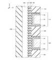
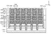
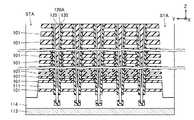
図7は、メモリダイMDの模式的な平面図である。図7に示す通り、メモリダイMDは、半導体基板100を備える。図示の例において、半導体基板100にはX方向に並ぶ2つのメモリセルアレイMCAが設けられる。メモリセルアレイMCAは、Y方向に並ぶ複数のメモリブロックMBを備える。メモリブロックMBは、Y方向に並ぶ2つのフィンガー構造FSを備える。フィンガー構造FSは、Y方向に並ぶ2つのストリングユニットSUを備える。 FIG. 7 is a schematic plan view of the memory die MD. As shown in FIG. 7, the memory die MD includes a
図8は、図7のAで示した部分の模式的な拡大図である。図8に示す通り、Y方向に並ぶ2つのフィンガー構造FSの間には、X方向に延伸するブロック構造間絶縁層STが設けられる。フィンガー構造FSは、X方向に延伸する導電層110と、X方向及びY方向に所定のパターンで並ぶ複数の半導体層120と、を備える。また、Y方向に並ぶ2つのストリングユニットSUの間には、X方向に延伸するサブブロック間絶縁層SHEが設けられる。また、図8には、X方向に並び、Y方向に延伸する複数のビット線BLを図示している。これら複数のビット線BLは、それぞれ、各ストリングユニットSUに含まれる1の半導体層120に接続されている。 FIG. 8 is a schematic enlarged view of the portion shown by A in FIG. 7. As shown in FIG. 8, an inter-block structure insulating layer ST extending in the X direction is provided between the two finger structure FSs arranged in the Y direction. The finger structure FS includes a
図9は、図8に示す構造をB−B´線で切断し、矢印の方向に見た模式的な断面図である。図10は、図9のCで示した部分の模式的な拡大図である。 FIG. 9 is a schematic cross-sectional view of the structure shown in FIG. 8 cut along the BB'line and viewed in the direction of the arrow. FIG. 10 is a schematic enlarged view of the portion shown by C in FIG.
図9に示す通り、ストリングユニットSUは、Z方向に並ぶ複数の導電層110と、Z方向に延伸する複数の半導体層120と、複数の導電層110及び複数の半導体層120の間にそれぞれ設けられた複数のゲート絶縁膜130と、を備える。 As shown in FIG. 9, the string unit SU is provided between the plurality of
導電層110は、メモリセルMC等のゲート電極及びワード線WL等として機能する。導電層110は、X方向に延伸する略板状の導電層である。導電層110は、例えば図10に示す様に、窒化チタン(TiN)等のバリア導電膜116及びタングステン(W)等の金属膜115の積層膜等を含んでいても良い。また、導電層110は、例えば、リン(P)又はホウ素(B)等の不純物を含む多結晶シリコン等を含んでいても良い。Z方向に並ぶ複数の導電層110の間には、酸化シリコン(SiO2)等の絶縁層101が設けられている。The
導電層110の下方には、図9に示す様に、導電層111が設けられている。導電層111は、ソース側選択トランジスタSTSのゲート電極及びソース選択線SGSとして機能する。導電層111は、例えば、リン(P)等の不純物を含む多結晶シリコン等を含んでいても良い。また、導電層111及び導電層110の間には、酸化シリコン(SiO2)等の絶縁層101が設けられている。As shown in FIG. 9, a
導電層111の下方には、導電層112が設けられている。導電層112は、ソース線SLとして機能する。導電層112は、例えば、タングステンシリサイド(WSi)等の金属を含む導電層113と、リン(P)等のN型の不純物を含む多結晶シリコン等の導電層114と、を含んでいても良い。また、導電層112及び導電層111の間には、酸化シリコン(SiO2)等の絶縁層101が設けられている。A
半導体層120は、1つのメモリストリングMS(図1)に含まれる複数のメモリセルMC及び選択トランジスタ(STD、STS)のチャネル領域として機能する。半導体層120は、例えば、多結晶シリコン(Si)等の半導体層である。半導体層120は、例えば、略有底円筒状の形状を有し、中心部分には酸化シリコン等の絶縁層125が設けられている。また、半導体層120の外周面は、それぞれ導電層110によって囲われている。 The
半導体層120の下端部及び上端部には、リン(P)等のN型の不純物を含む不純物領域121,122が設けられている。また、不純物領域121,122の間には、リン(P)等のN型の不純物を含まない領域123が設けられている。不純物領域121は、導電層114に接続され、導電層111と対向している。不純物領域122は、図示しないコンタクトを介してビット線BL(図8)に接続されている。領域123は、導電層111及びZ方向に並ぶ全ての導電層110に対向している。領域123のうち、ドレイン選択線SGDとして動作する導電層110と対向する部分は、ドレイン側選択トランジスタSTDのチャネル領域として機能する。領域123のうち、ワード線WLとして動作する導電層110と対向する部分は、メモリセルMCのチャネル領域として機能する。領域123のうち、ソース選択線SGSとして動作する導電層110と対向する部分、及び、導電層111と対向する部分は、ソース側選択トランジスタSTSのチャネル領域として機能する。
ゲート絶縁膜130は、半導体層120の外周面及び下端を覆う略有底円筒状の形状を有する。ただし、ゲート絶縁膜130は、半導体層120及び導電層114の接続部分には設けられていない。 The
ゲート絶縁膜130は、例えば図10に示す通り、半導体層120及び導電層110の間に積層されたトンネル絶縁膜131、電荷蓄積膜132、ブロック絶縁膜133、及び、ブロック絶縁膜134を備える。トンネル絶縁膜131及びブロック絶縁膜133は、例えば、酸化シリコン(SiO2)等の絶縁膜である。電荷蓄積膜132は、例えば、窒化シリコン(Si3N4)等の電荷を蓄積可能な膜である。ブロック絶縁膜134は、例えば、アルミナ(Al3O4)等の金属酸化物を含む絶縁膜である。トンネル絶縁膜131、電荷蓄積膜132、及び、ブロック絶縁膜133は略円筒状の形状を有し、半導体層120の外周面に沿ってZ方向に延伸する。ブロック絶縁膜134は、例えば、導電層110の上面、下面及び側面に沿って形成されている。As shown in FIG. 10, for example, the
尚、図10には、ゲート絶縁膜130が窒化シリコン等の電荷蓄積膜132を備える例を示した。しかしながら、ゲート絶縁膜130は、例えば、N型又はP型の不純物を含む多結晶シリコン等のフローティングゲートを備えていても良い。 Note that FIG. 10 shows an example in which the
次に、図9を参照して、本実施形態に係る半導体記憶装置について、より詳しく説明する。 Next, the semiconductor storage device according to the present embodiment will be described in more detail with reference to FIG.
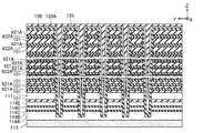
図9に示す様に、本実施形態に係る半導体層120は、下方に位置する部分ほど外径が小さく、上方に位置する部分ほど外径が大きい。例えば、半導体層120の領域123には、小領域126、小領域126よりも下方に位置する小領域127、及び、小領域127よりも下方に位置する小領域128が含まれる。小領域126における半導体層120の外径は、所定の幅W121よりも大きい。小領域127における半導体層120の外径は、所定の幅W121よりも小さく、所定の幅W122よりも大きい。小領域128における半導体層120の外径は、所定の幅W122よりも小さい。As shown in FIG. 9, the
また、図9に示す様に、半導体層120の小領域126に対向する導電層110は、間隔D111を介してZ方向に並んでいる。また、半導体層120の小領域127に対向する導電層110は、間隔D111よりも小さい間隔D112を介してZ方向に並んでいる。また、半導体層120の小領域128に対向する導電層110は、間隔D112よりも小さい間隔D113を介してZ方向に並んでいる。Further, as shown in FIG. 9, the
また、図9に示す様に、半導体層120の小領域126に対向する導電層110の間に設けられた絶縁層101は、Z方向において厚みT111を有する。また、半導体層120の小領域127に対向する導電層110の間に設けられた絶縁層101は、Z方向において厚みT111よりも小さい厚みT112を有する。また、半導体層120の小領域128に対向する導電層110の間に設けられた絶縁層101は、Z方向において厚みT112よりも小さい厚みT113を有する。Further, as shown in FIG. 9, the insulating
[効果]
図8に示す様に、本実施形態に係る導電層110には複数の貫通孔が設けられており、半導体層120はこの貫通孔の内部に設けられている。また、図9に示す様に、本実施形態に係る半導体層120は、下方に位置する部分ほど外径が小さく、上方に位置する部分ほど外径が大きい。従って、下方に位置する導電層110ほど小さい貫通孔を有し、上方に位置する導電層110ほど大きい貫通孔を有する。この様な態様においては、下方に位置する導電層110ほど配線抵抗が小さくなり、上方に位置する導電層110ほど配線抵抗が大きくなる。この様な態様において導電層110をZ方向に均等な間隔で配置した場合、下方に位置する導電層110ほど電圧の転送速度が大きくなり、上方に位置する導電層110ほど電圧の転送速度が小さくなることが考えられる。[effect]
As shown in FIG. 8, the
ここで、上述の通り、本実施形態においては、比較的上方に設けられた導電層110は、比較的大きい間隔D111を介してZ方向に並んでいる。これにより、導電層110間の静電容量を削減して、電圧の転送速度を大きくすることが可能である。また、本実施形態においては、比較的下方に設けられた導電層110は、比較的小さい間隔D113を介してZ方向に並んでいる。これにより、Z方向に積層された複数の導電層110の間で電圧の転送速度を揃えつつ、半導体記憶装置のZ方向における高集積化を図ることが可能である。Here, as described above, in the present embodiment, the
[第2実施形態]
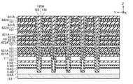
次に、図11を参照して、第2実施形態に係る半導体記憶装置について説明する。第2実施形態に係る半導体記憶装置は、基本的には第1実施形態に係る半導体記憶装置と同様に構成されている。ただし、第2実施形態に係る半導体記憶装置は、導電層110のかわりに、導電層210を備えている。[Second Embodiment]
Next, the semiconductor storage device according to the second embodiment will be described with reference to FIG. The semiconductor storage device according to the second embodiment is basically configured in the same manner as the semiconductor storage device according to the first embodiment. However, the semiconductor storage device according to the second embodiment includes the
導電層210は、基本的には第1実施形態に係る導電層110と同様に構成されている。ただし、半導体層120の小領域126に対向する導電層210は、Z方向において厚みT211を有する。また、半導体層120の小領域127に対向する導電層210は、Z方向において、厚みT211よりも小さい厚みT212を有する。また、半導体層120の小領域128に対向する導電層210は、Z方向において、厚みT212よりも小さい厚みT213を有する。The
この様な構成によれば、比較的上方に設けられた導電層210の配線抵抗を削減して、電圧の転送速度を大きくすることが可能である。また、本実施形態においては、比較的下方に設けられた導電層210のZ方向における厚みを削減して、Z方向に積層された複数の導電層210の間で電圧の転送速度を揃えつつ、半導体記憶装置のZ方向における高集積化を図ることが可能である。 According to such a configuration, it is possible to reduce the wiring resistance of the
[第3実施形態]
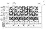
次に、図12を参照して、第3実施形態に係る半導体記憶装置について説明する。第3実施形態に係る半導体記憶装置は、基本的には第1実施形態に係る半導体記憶装置と同様に構成されている。ただし、第3実施形態に係る半導体記憶装置は、導電層110のかわりに導電層310を備え、絶縁層101のかわりに絶縁層301を備え、半導体層120のかわりに半導体層320を備えている。[Third Embodiment]
Next, the semiconductor storage device according to the third embodiment will be described with reference to FIG. The semiconductor storage device according to the third embodiment is basically configured in the same manner as the semiconductor storage device according to the first embodiment. However, the semiconductor storage device according to the third embodiment includes a
導電層310、絶縁層301及び半導体層320は、基本的には、第1実施形態に係る導電層110、絶縁層101及び半導体層120と同様に構成されている。 The
ただし、本実施形態に係る半導体層320は、下端近傍に位置する部分及び上端近傍に位置する部分において外径が小さく、その間に位置する部分において外径が大きい。例えば、半導体層320の領域323には、小領域326、小領域326よりも下方に位置する小領域327、小領域327よりも下方に位置する小領域328、及び、小領域326よりも上方に位置する小領域329が含まれる。小領域326における半導体層320の外径は、所定の幅W321よりも大きい。小領域327における半導体層320の外径は、所定の幅W321よりも小さく、所定の幅W322よりも大きい。小領域328における半導体層320の外径は、所定の幅W322よりも小さい。小領域329における半導体層320の外径は、所定の幅W321よりも小さく、所定の幅W322よりも大きい。However, the
また、図12に示す様に、半導体層320の小領域326に対向する導電層310は、間隔D311を介してZ方向に並んでいる。また、半導体層320の小領域327に対向する導電層310は、間隔D311よりも小さい間隔D312を介してZ方向に並んでいる。また、半導体層320の小領域328に対向する導電層310は、間隔D312よりも小さい間隔D313を介してZ方向に並んでいる。また、半導体層320の小領域329に対向する導電層310は、間隔D311よりも小さく間隔D312よりも大きい間隔D314を介してZ方向に並んでいる。Further, as shown in FIG. 12, the
また、図12に示す様に、半導体層320の小領域326に対向する導電層310の間に設けられた絶縁層301は、Z方向において厚みT311を有する。また、半導体層320の小領域327に対向する導電層310の間に設けられた絶縁層301は、Z方向において厚みT311よりも小さい厚みT312を有する。また、半導体層320の小領域328に対向する導電層310の間に設けられた絶縁層301は、Z方向において厚みT312よりも小さい厚みT313を有する。また、半導体層320の小領域329に対向する導電層310の間に設けられた絶縁層301は、Z方向において厚みT311よりも小さく厚みT312よりも大きい厚みT314を有する。Further, as shown in FIG. 12, the insulating
[第4実施形態]
次に、図13を参照して、第4実施形態に係る半導体記憶装置について説明する。第4実施形態に係る半導体記憶装置は、基本的には第3実施形態に係る半導体記憶装置と同様に構成されている。ただし、第4実施形態に係る半導体記憶装置は、導電層310のかわりに、導電層410を備えている。[Fourth Embodiment]
Next, the semiconductor storage device according to the fourth embodiment will be described with reference to FIG. The semiconductor storage device according to the fourth embodiment is basically configured in the same manner as the semiconductor storage device according to the third embodiment. However, the semiconductor storage device according to the fourth embodiment includes the
導電層410は、基本的には第3実施形態に係る導電層310と同様に構成されている。ただし、半導体層320の小領域326に対向する導電層410は、Z方向において厚みT411を有する。また、半導体層120の小領域327に対向する導電層410は、Z方向において、厚みT411よりも小さい厚みT412を有する。また、半導体層120の小領域328に対向する導電層410は、Z方向において、厚みT412よりも小さい厚みT413を有する。また、半導体層320の小領域329に対向する導電層410は、Z方向において、厚みT411よりも小さく厚みT412よりも大きい厚みT414を有する。The
[第5実施形態]
次に、図14を参照して、第5実施形態に係る半導体記憶装置について説明する。第5実施形態に係る半導体記憶装置は、基本的には第1実施形態に係る半導体記憶装置と同様に構成されている。ただし、第5実施形態に係る半導体記憶装置は、導電層110に加えて導電層510を備え、絶縁層101に加えて絶縁層501を備え、半導体層120のかわりに半導体層520を備えている。[Fifth Embodiment]
Next, the semiconductor storage device according to the fifth embodiment will be described with reference to FIG. The semiconductor storage device according to the fifth embodiment is basically configured in the same manner as the semiconductor storage device according to the first embodiment. However, the semiconductor storage device according to the fifth embodiment includes a
導電層510及び絶縁層501は、基本的には導電層110及び絶縁層101と同様に構成されている。ただし、導電層510及び絶縁層501は、導電層110及び絶縁層101よりも上方に設けられている。 The
半導体層520は、基本的には半導体層120と同様に構成されている。ただし、半導体層520は、下方に位置する領域521と、上方に位置する領域522と、領域521の上端及び領域522の下端に接続された領域523と、を備える。 The
領域521の外周面は、それぞれ導電層110によって囲われており、これら複数の導電層110と対向している。領域521の下端部には、リン(P)等のN型の不純物を含む不純物領域121が設けられている。また、不純物領域121の上方には、リン(P)等のN型の不純物を含まない領域524が設けられている。領域524のうち、ワード線WLとして動作する導電層110と対向する部分は、メモリセルMCのチャネル領域として機能する。領域524のうち、ソース選択線SGSとして動作する導電層110と対向する部分、及び、導電層111と対向する部分は、ソース側選択トランジスタSTSのチャネル領域として機能する。 The outer peripheral surface of the region 521 is surrounded by the
領域522の外周面は、それぞれ導電層510によって囲われており、これら複数の導電層510と対向している。領域522の上端部には、リン(P)等のN型の不純物を含む不純物領域122が設けられている。また、不純物領域122の下方には、リン(P)等のN型の不純物を含まない領域525が設けられている。領域525のうち、ワード線WLとして動作する導電層510と対向する部分は、メモリセルMCのチャネル領域として機能する。領域525のうち、ドレイン選択線SGDとして動作する導電層510と対向する部分は、ドレイン側選択トランジスタSTDのチャネル領域として機能する。 The outer peripheral surface of the
また、本実施形態に係る半導体層520において、領域523の外径W521は、領域521,522の外径の最大値よりも大きい。また、領域521,522は、下方に位置する部分ほど外径が小さく、上方に位置する部分ほど外径が大きい。例えば、半導体層520の領域524には、小領域526、小領域526よりも下方に位置する小領域527、及び、小領域527よりも下方に位置する小領域528が含まれる。小領域526における半導体層520の外径は、上記外径W521よりも小さく、所定の幅W522よりも大きい。小領域527における半導体層520の外径は、所定の幅W522よりも小さく、所定の幅W523よりも大きい。小領域528における半導体層520の外径は、所定の幅W523よりも小さい。また、例えば、半導体層520の領域525には、小領域529、小領域529よりも下方に位置する小領域530、及び、小領域530よりも下方に位置する小領域531が含まれる。小領域529における半導体層520の外径は、上記外径W521よりも小さく、所定の幅W524よりも大きい。小領域530における半導体層520の外径は、所定の幅W524よりも小さく、所定の幅W525よりも大きい。小領域531における半導体層520の外径は、所定の幅W525よりも小さい。Further, in the
また、図14に示す様に、半導体層520の小領域526に対向する半導体層520は、間隔D511を介してZ方向に並んでいる。また、半導体層520の小領域527に対向する半導体層520は、間隔D511よりも小さい間隔D512を介してZ方向に並んでいる。また、半導体層520の小領域528に対向する半導体層520は、間隔D512よりも小さい間隔D513を介してZ方向に並んでいる。Further, as shown in FIG. 14, the semiconductor layers 520 facing the
また、図14に示す様に、半導体層520の小領域529に対向する導電層510は、間隔D514を介してZ方向に並んでいる。また、半導体層520の小領域530に対向する導電層510は、間隔D514よりも小さい間隔D515を介してZ方向に並んでいる。また、半導体層520の小領域531に対向する導電層510は、間隔D515よりも小さい間隔D516を介してZ方向に並んでいる。Further, as shown in FIG. 14, the
尚、間隔D511は、間隔D514と等しくても良い。また、間隔D512は、間隔D515と等しくても良い。また、間隔D513は、間隔D516と等しくても良い。The interval D511 may be equal to the interval D514. Further, the interval D512 may be equal to the interval D515. Further, the interval D513 may be equal to the interval D516.
また、図14に示す様に、半導体層520の小領域526に対向する導電層110の間に設けられた絶縁層101は、Z方向において厚みT511を有する。また、半導体層520の小領域527に対向する導電層110の間に設けられた絶縁層101は、Z方向において厚みT511よりも小さい厚みT512を有する。また、半導体層520の小領域528に対向する導電層110の間に設けられた絶縁層101は、Z方向において厚みT512よりも小さい厚みT513を有する。Further, as shown in FIG. 14, the insulating
また、図14に示す様に、半導体層520の小領域529に対向する導電層510の間に設けられた絶縁層501は、Z方向において厚みT514を有する。また、半導体層520の小領域530に対向する導電層510の間に設けられた絶縁層501は、Z方向において厚みT514よりも小さい厚みT515を有する。また、半導体層520の小領域531に対向する導電層510の間に設けられた絶縁層501は、Z方向において厚みT515よりも小さい厚みT516を有する。Further, as shown in FIG. 14, the insulating
尚、厚みT511は、厚みT514と等しくても良い。また、厚みT512は、厚みT515と等しくても良い。また、厚みT513は、厚みT516と等しくても良い。The thickness T511 may be equal to the thickness T514. Further, the thickness T512 may be equal to the thickness T515. Further, the thickness T513 may be equal to the thickness T516.
尚、図14の例において、半導体層520の領域521,522は、それぞれ、第1実施形態に係る半導体層120と同様に、下方に位置する部分ほど外径が小さく、上方に位置する部分ほど外径が大きくなるように構成されていた。しかしながら、領域521,522は、例えば第3実施形態に係る半導体層320と同様に、下端近傍に位置する部分及び上端近傍に位置する部分において外径が小さく、その間に位置する部分において外径が大きくなるように構成されても良い。 In the example of FIG. 14, the
また、図14に例示する半導体記憶装置は、導電層110及び絶縁層101、並びに、これらと同様に構成された導電層510及び絶縁層501を備えていた。しかしながら、図14に例示する半導体記憶装置は、例えば、導電層210及び絶縁層101、並びに、これらと同様に構成された導電層及び絶縁層を備えていても良い。また、例えば、導電層410及び絶縁層101、並びに、これらと同様に構成された導電層及び絶縁層を備えていても良い。 Further, the semiconductor storage device illustrated in FIG. 14 includes a
[第6実施形態]
次に、図15を参照して、第6実施形態に係る半導体記憶装置について説明する。第6実施形態に係る半導体記憶装置は、基本的には第2実施形態に係る半導体記憶装置と同様に構成されている。ただし、第6実施形態に係る半導体記憶装置は、図15に示す様な構造を備えている。図15に示す様な構造は、例えば、メモリセルアレイMCAが設けられる領域の内部に設けられていても良いし、メモリセルアレイMCAが設けられる領域の外部に設けられていても良い。また、図15にはYZ断面を例示しているが、本実施形態に係る半導体記憶装置は、図15に示す様なXZ断面を備えていても良い。[Sixth Embodiment]
Next, the semiconductor storage device according to the sixth embodiment will be described with reference to FIG. The semiconductor storage device according to the sixth embodiment is basically configured in the same manner as the semiconductor storage device according to the second embodiment. However, the semiconductor storage device according to the sixth embodiment has a structure as shown in FIG. The structure as shown in FIG. 15 may be provided inside, for example, the area where the memory cell array MCA is provided, or may be provided outside the area where the memory cell array MCA is provided. Further, although the YZ cross section is illustrated in FIG. 15, the semiconductor storage device according to the present embodiment may have an XZ cross section as shown in FIG.
図15に示す構造は、積層体LB1と、積層体LB2と、を含む。 The structure shown in FIG. 15 includes a laminated body LB1 and a laminated body LB2.
積層体LB1は、Z方向に順に並ぶ導電層613、導電層614、絶縁層601、及び、導電層611を含む。また、積層体LB1は、Z方向に並ぶ複数の導電層610を含む。また、Z方向に並ぶ複数の導電層610の間には、絶縁層601が設けられている。これらの導電層613、導電層614、絶縁層601、導電層611及び導電層610は、それぞれ、導電層113、導電層114、絶縁層101、導電層111及び導電層110と同様に構成されている。尚、Z方向に並ぶ導電層610及び絶縁層601の数、並びに、導電層610及び絶縁層601のZ方向における膜厚は、それぞれ、Z方向に並ぶ導電層210及び絶縁層101の数、並びに、導電層210及び絶縁層101のZ方向における膜厚と等しい。 The laminated body LB1 includes a
積層体LB2は、Z方向に順に並ぶ導電層613、導電層614A、絶縁層614B、半導体層614C、絶縁層614D、導電層614E、絶縁層601、及び、導電層611を含む。また、積層体LB2は、Z方向に並ぶ複数の絶縁層620を含む。また、Z方向に並ぶ複数の絶縁層620の間には、絶縁層601が設けられている。尚、Z方向に並ぶ絶縁層620及び絶縁層601の数、並びに、絶縁層620及び絶縁層601のZ方向における膜厚は、それぞれ、Z方向に並ぶ導電層210及び絶縁層101の数、並びに、導電層210及び絶縁層101のZ方向における膜厚と等しい。 The laminated body LB2 includes a
積層体LB1,LB2において、導電層613、導電層611及び複数の絶縁層601は、連続的に一体として形成されている。また、導電層614は、導電層614A,614Eと、連続的に一体として形成されている。また、絶縁層614B、半導体層614C、絶縁層614DのX方向の側面及びY方向の側面の少なくとも一方は、導電層614に接続されている。また、絶縁層620のX方向の側面及びY方向の側面の少なくとも一方は、導電層610に接続されている。 In the laminated bodies LB1 and LB2, the
絶縁層620は、例えば、窒化シリコン(Si3N4)等の絶縁膜621を含む。また、複数の絶縁層620のうちの少なくとも一部は、窒化シリコン等の絶縁膜622を含む。絶縁膜622は、絶縁膜621よりも大きい密度、絶縁膜621よりも小さい水素の含有量、及び、絶縁膜621よりも小さいリン酸等に対するエッチングレートの、少なくとも一つを有する。The insulating
ここで、図示の例では、Z方向における厚みT211を有する絶縁層620は、絶縁膜621及び絶縁膜622を含む。この絶縁膜621は、Z方向における厚みT621を有する。また、この絶縁膜622は、Z方向における厚みT631を有する。Here, in the illustrated example, theinsulating layer 620 having the thickness T 211 in the Z direction includes the insulating
また、図示の例では、Z方向における厚みT212を有する絶縁層620は、絶縁膜621及び絶縁膜622を含む。この絶縁膜621は、Z方向における厚みT621を有する。また、この絶縁膜622は、Z方向における厚みT632を有する。厚みT632は、厚みT631よりも小さい。Further, in the illustrated example, theinsulating layer 620 having the thickness T 212 in the Z direction includes the insulating
また、図示の例では、Z方向における厚みT213を有する絶縁層620は、絶縁膜621を含む。この絶縁膜621は、Z方向における厚みT621を有する。尚、図示の例において、厚みT621は、厚みT213と等しい。即ち、これらの絶縁層620は、絶縁膜622を備えていない。Further, in the illustrated example, theinsulating layer 620 having the thickness T 213 in the Z direction includes the insulating
次に、図16〜図26を参照して、本実施形態に係る半導体記憶装置の製造方法について説明する。図16〜図26は、同製造方法について説明するための模式的な断面図である。 Next, a method of manufacturing the semiconductor storage device according to the present embodiment will be described with reference to FIGS. 16 to 26. 16 to 26 are schematic cross-sectional views for explaining the manufacturing method.
同製造方法においては、例えば図16に示す様に、導電層113、シリコン等の半導体層114A、酸化シリコン等の犠牲層114B、シリコン等の犠牲層114C、酸化シリコン等の犠牲層114D、シリコン等の半導体層114E、絶縁層101及び導電層111を形成する。また、複数の絶縁層101及び複数の犠牲層621Aを交互に形成する。また、絶縁層601、犠牲層622A及び犠牲層621Aを、複数回順番に形成する。この工程は、例えば、CVD(Chemical Vapor Deposition)等の方法によって行われる。 In the same manufacturing method, for example, as shown in FIG. 16, the
犠牲層621A,622Aは、例えば、窒化シリコン(Si3N4)等を含む。犠牲層622Aは、犠牲層621Aよりも大きい密度、犠牲層621Aよりも小さい水素の含有量、及び、犠牲層621Aよりも小さいリン酸等の薬液に対するエッチングレートの、少なくとも一つを有する。The
次に、例えば図17に示す様に、複数の絶縁層101及び複数の犠牲層621A,622A、導電層111、半導体層114E、犠牲層114D、犠牲層114C及び犠牲層114Bを貫通してZ方向に延伸する開口MHを形成する。この工程は、例えば、RIE(Reactive Ion Etching)等の方法によって行われる。 Next, as shown in FIG. 17, for example, the insulating
次に、例えば図18に示す様に、開口MHの内部、及び、最上層に位置する絶縁層101の上面に、ゲート絶縁膜130、シリコン等の半導体層120A及び絶縁層125を形成する。この工程は、例えば、CVD等の方法によって行われる。 Next, for example, as shown in FIG. 18, a
次に、例えば図19に示す様に、ゲート絶縁膜130、シリコン等の半導体層120A及び絶縁層125のうち、最上層に位置する絶縁層101の上面に設けられた部分を除去する。この工程は、例えば、RIEによるエッチバック等の方法によって行われる。 Next, as shown in FIG. 19, for example, of the
次に、例えば図20に示す様に、複数の絶縁層101及び複数の犠牲層621A,622A、導電層111、半導体層114E及び犠牲層114Dを貫通してX方向及びZ方向に延伸する開口STAを形成する。この工程は、例えば、RIE等の方法によって行われる。 Next, as shown in FIG. 20, for example, an opening STA extending in the X and Z directions through the plurality of insulating
次に、例えば図21に示す様に、開口STAのY方向の側面に、窒化シリコン等の保護膜STBを形成する。この工程は、例えば、CVD等の方法によって行われる。 Next, for example, as shown in FIG. 21, a protective film STB such as silicon nitride is formed on the side surface of the opening STA in the Y direction. This step is performed by, for example, a method such as CVD.
次に、例えば図22に示す様に、犠牲層114C、犠牲層114B及び犠牲層114Dを除去する。この工程は、例えば、ウェットエッチング等の方法によって行われる。 Next, for example, as shown in FIG. 22, the
次に、例えば図23に示す様に、ゲート絶縁膜130の一部を除去する。この工程は、例えば、ウェットエッチング等の方法によって行われる。 Next, for example, as shown in FIG. 23, a part of the
次に、例えば図24に示す様に、導電層114を形成する。例えば、エピタキシャル成長等の方法によって、半導体層114Aの上面及び半導体層114Eの下面に、リン等の不純物を含むシリコンを形成する。 Next, for example, as shown in FIG. 24, the
次に、例えば図25に示す様に、保護膜STBを除去する。この工程は、例えば、ウェットエッチング等の方法によって行われる。 Next, for example, as shown in FIG. 25, the protective film STB is removed. This step is performed by, for example, a method such as wet etching.
次に、例えば図25に示す様に、犠牲層621A,622Aを除去する。この工程は、例えば、リン酸等の薬液を用いたウェットエッチング等の方法によって行われる。 Next, as shown in FIG. 25, for example, the
この際、例えば図26に示す様に、一部の領域に形成された犠牲層621A,622Aは除去されずに残存する。この様な犠牲層621A,622Aは、絶縁層620となる。 At this time, for example, as shown in FIG. 26, the
その後、CVD等の方法によって導電層110、及び、ブロック構造間絶縁層ST(図22)を形成する。また、RIE及びCVD等の方法によってサブブロック間絶縁層SHE(図22)を形成する。これにより、図4等を参照して説明した構造が形成される。 After that, the
図27は、比較例に係る製造方法を示す模式的な断面図である。比較例に係る製造方法は、基本的には第6実施形態に係る製造方法と同様である。ただし、第6実施形態では、図16に対応する工程において犠牲層622Aが形成されず、そのかわりに犠牲層621Aが形成される。上層に設けられた犠牲層621Aほど、Z方向における厚みが大きい。 FIG. 27 is a schematic cross-sectional view showing a manufacturing method according to a comparative example. The manufacturing method according to the comparative example is basically the same as the manufacturing method according to the sixth embodiment. However, in the sixth embodiment, the
ここで、例えば図25及び図26を参照して説明した工程では、ウェットエッチング等の方法によって犠牲層621Aを除去することとなる。この際、図27に示す様な態様では、Z方向における厚みが大きい犠牲層621Aは除去される速度が比較的大きく、Z方向における厚みが小さい犠牲層621Aは除去される速度が比較的小さくなる場合がある。 Here, for example, in the steps described with reference to FIGS. 25 and 26, the
この様な態様では、例えば図28に示す様に、下方に位置する犠牲層621Aが除去される前に上方に位置する犠牲層621Aが完全に除去されてしまい、ゲート絶縁膜130がウェットエッチングの薬液に長時間さらされてしまい、ゲート絶縁膜130の膜質が劣化してしまう場合がある。 In such an embodiment, for example, as shown in FIG. 28, the
そこで、図16を参照して説明した様に、比較的下方に位置する部分については犠牲層621Aの単層膜を使用し、比較的上方に位置する部分については犠牲層621A及びこの犠牲層621Aよりもエッチングレートが小さい犠牲層622Aを含む積層膜を使用している。また、犠牲層621AのZ方向における厚みT621(図15)を略同一の大きさとしている。Therefore, as described with reference to FIG. 16, the monolayer film of the
この様な方法によれば、例えば図29に示す様に、下方に位置する犠牲層621Aと、上方に位置する犠牲層621Aとの間で、エッチングの速度を揃えることが可能である。これにより、ゲート絶縁膜130の膜質の劣化を抑制可能である。 According to such a method, as shown in FIG. 29, for example, it is possible to make the etching speed uniform between the
尚、上述の例では、図11に例示した様な構造のメモリセルアレイMCAと、図15に例示した様な構造と、を備える半導体記憶装置を例示した。しかしながら、本実施形態に係る半導体記憶装置は、例えば、図13に例示した様な構造のメモリセルアレイMCAを備えていても良い。この様な場合、Z方向に並ぶ導電層610及び絶縁層601の数、並びに、導電層610及び絶縁層601のZ方向における膜厚は、それぞれ、Z方向に並ぶ導電層410及び絶縁層101の数、並びに、導電層410及び絶縁層101のZ方向における膜厚と等しい。また、Z方向に並ぶ絶縁層620及び絶縁層601の数、並びに、絶縁層620及び絶縁層601のZ方向における膜厚は、それぞれ、Z方向に並ぶ導電層410及び絶縁層101の数、並びに、導電層410及び絶縁層101のZ方向における膜厚と等しい。 In the above example, a semiconductor storage device including a memory cell array MCA having a structure as illustrated in FIG. 11 and a structure as illustrated in FIG. 15 is illustrated. However, the semiconductor storage device according to the present embodiment may include, for example, a memory cell array MCA having a structure as illustrated in FIG. In such a case, the number of the
[その他の実施形態]
以上、第1〜第6の実施形態に係る半導体記憶装置について説明した。しかしながら、これらの実施形態に係る半導体記憶装置はあくまでも例示であり、具体的な構成、動作等は適宜調整可能である。[Other Embodiments]
The semiconductor storage device according to the first to sixth embodiments has been described above. However, the semiconductor storage devices according to these embodiments are merely examples, and specific configurations, operations, and the like can be appropriately adjusted.
例えば、第1〜第6の実施形態では、いずれも半導体層120等の外径のばらつきに応じて絶縁層101等のZ方向における厚みを3段階に調整していた。しかしながら、この様な態様は例示に過ぎず、具体的な態様は適宜調整可能である。例えば、絶縁層101等のZ方向における厚みを2段階に調整しても良いし、4段階以上に調整しても良い。 For example, in each of the first to sixth embodiments, the thickness of the insulating
また、例えば、第2及び第4の実施形態では、いずれも半導体層120等の外径のばらつきに応じて導電層210等のZ方向における厚みを3段階に調整していた。しかしながら、この様な態様は例示に過ぎず、具体的な態様は適宜調整可能である。例えば、導電層210等のZ方向における厚みを2段階に調整しても良いし、4段階以上に調整しても良い。 Further, for example, in the second and fourth embodiments, the thickness of the
[その他]
本発明のいくつかの実施形態を説明したが、これらの実施形態は例として提示したものであり、発明の範囲を限定することは意図していない。これら新規な実施形態は、その他の様々な形態で実施されることが可能であり、発明の要旨を逸脱しない範囲で、種々の省略、置き換え、変更を行うことが出来る。これら実施形態やその変形は、発明の範囲や要旨に含まれると共に、特許請求の範囲に記載された発明とその均等の範囲に含まれる。[others]
Although some embodiments of the present invention have been described, these embodiments are presented as examples and are not intended to limit the scope of the invention. These novel embodiments can be implemented in various other embodiments, and various omissions, replacements, and changes can be made without departing from the gist of the invention. These embodiments and modifications thereof are included in the scope and gist of the invention, and are also included in the scope of the invention described in the claims and the equivalent scope thereof.
MC…メモリセル、MCA…メモリセルアレイ、ADD…アドレスデータ、CMD…コマンドデータ、PC…周辺回路、P…パッド電極。 MC ... memory cell, MCA ... memory cell array, ADD ... address data, CMD ... command data, PC ... peripheral circuit, P ... pad electrode.
Claims (16)
Translated fromJapanese前記基板の表面と交差する第1方向に並び、前記第1方向と交差する第2方向に延伸する複数の導電層と、
前記第1方向に延伸し、前記複数の導電層を貫通する半導体層と
を備え、
前記半導体層は、
前記半導体層の第1方向における一端部と前記半導体層の第1方向における他端部との間に設けられ、前記第2方向における幅が第1の幅よりも大きい第1部分と、
前記第1部分と前記他端部との間に設けられ、前記第2方向における幅が前記第1の幅よりも小さく第2の幅よりも大きい第2部分と、
前記第2部分と前記他端部との間に設けられ、前記第2方向における幅が前記第2の幅よりも小さい第3部分と
を備え、
前記複数の導電層は、
前記第1部分と対向する第1導電層と、
前記第1導電層と前記第1方向において隣り合う第2導電層と、
前記第2部分と対向する第3導電層と、
前記第3導電層と前記第1方向において隣り合う第4導電層と、
前記第3部分と対向する第5導電層と、
前記第5導電層と前記第1方向において隣り合う第6導電層と
を含み、
前記第1導電層及び前記第2導電層の間の前記第1方向における距離を第1距離とし、
前記第3導電層及び前記第4導電層の間の前記第1方向における距離を第2距離とし、
前記第5導電層及び前記第6導電層の間の前記第1方向における距離を第3距離とすると、
前記第2距離は前記第1距離よりも小さく、
前記第3距離は前記第2距離よりも小さい
半導体記憶装置。With the board
A plurality of conductive layers aligned in a first direction intersecting the surface of the substrate and extending in a second direction intersecting the first direction.
A semiconductor layer extending in the first direction and penetrating the plurality of conductive layers is provided.
The semiconductor layer is
A first portion provided between one end of the semiconductor layer in the first direction and the other end of the semiconductor layer in the first direction and having a width larger than the first width in the second direction.
A second portion provided between the first portion and the other end and having a width in the second direction smaller than the first width and larger than the second width.
A third portion provided between the second portion and the other end portion and having a width in the second direction smaller than the second width is provided.
The plurality of conductive layers are
The first conductive layer facing the first portion and
The first conductive layer and the second conductive layer adjacent to each other in the first direction,
A third conductive layer facing the second portion and
The third conductive layer and the fourth conductive layer adjacent to each other in the first direction,
A fifth conductive layer facing the third portion and
The fifth conductive layer and the sixth conductive layer adjacent to each other in the first direction are included.
The distance between the first conductive layer and the second conductive layer in the first direction is defined as the first distance.
The distance between the third conductive layer and the fourth conductive layer in the first direction is defined as the second distance.
Let the distance between the fifth conductive layer and the sixth conductive layer in the first direction be the third distance.
The second distance is smaller than the first distance,
A semiconductor storage device in which the third distance is smaller than the second distance.
前記第2導電層の前記第1方向における厚みを第2の厚みとし、
前記第3導電層の前記第1方向における厚みを第3の厚みとし、
前記第4導電層の前記第1方向における厚みを第4の厚みとし、
前記第5導電層の前記第1方向における厚みを第5の厚みとし、
前記第6導電層の前記第1方向における厚みを第6の厚みとすると、
前記第3の厚み及び前記第4の厚みは、前記第1の厚み及び前記第2の厚みよりも小さく、
前記第5の厚み及び前記第6の厚みは、前記第3の厚み及び前記第4の厚みよりも小さい
請求項1記載の半導体記憶装置。The thickness of the first conductive layer in the first direction is defined as the first thickness.
The thickness of the second conductive layer in the first direction is defined as the second thickness.
The thickness of the third conductive layer in the first direction is defined as the third thickness.
The thickness of the fourth conductive layer in the first direction is defined as the fourth thickness.
The thickness of the fifth conductive layer in the first direction is defined as the fifth thickness.
Assuming that the thickness of the sixth conductive layer in the first direction is the sixth thickness,
The third thickness and the fourth thickness are smaller than the first thickness and the second thickness.
The semiconductor storage device according to claim 1, wherein the fifth thickness and the sixth thickness are smaller than the third thickness and the fourth thickness.
前記複数の導電層は、
前記第4部分と対向する第7導電層と、
前記第7導電層と前記第1方向において隣り合う第8導電層と
を含み、
前記第7導電層及び前記第8導電層の間の前記第1方向における距離を第4距離とすると、
前記第4距離は前記第1距離よりも小さい
請求項1又は2記載の半導体記憶装置。The semiconductor layer is provided between the first portion and one end portion of the semiconductor layer in the first direction, and includes a fourth portion whose width in the second direction is smaller than the second width.
The plurality of conductive layers are
A seventh conductive layer facing the fourth portion and
The seventh conductive layer and the eighth conductive layer adjacent to each other in the first direction are included.
Assuming that the distance between the 7th conductive layer and the 8th conductive layer in the first direction is the fourth distance,
The semiconductor storage device according to claim 1 or 2, wherein the fourth distance is smaller than the first distance.
前記第2導電層の前記第1方向における厚みを第2の厚みとし、
前記第7導電層の前記第1方向における厚みを第7の厚みとし、
前記第8導電層の前記第1方向における厚みを第8の厚みとすると、
前記第7の厚み及び前記第8の厚みは、前記第1の厚み及び前記第2の厚みよりも小さい
請求項3記載の半導体記憶装置。The thickness of the first conductive layer in the first direction is defined as the first thickness.
The thickness of the second conductive layer in the first direction is defined as the second thickness.
The thickness of the seventh conductive layer in the first direction is defined as the seventh thickness.
Assuming that the thickness of the eighth conductive layer in the first direction is the eighth thickness,
The semiconductor storage device according to claim 3, wherein the seventh thickness and the eighth thickness are smaller than the first thickness and the second thickness.
前記第1方向に並び、前記第2方向に延伸する複数の絶縁層と
を備え、
前記複数の導電層の、
a(aは自然数)番目の導電層を前記第1導電層とし、
a+1番目の導電層を前記第2導電層とし、
前記複数の他の導電層の、
a番目の導電層を第9導電層とし、
a+1番目の導電層を第10導電層とし、
前記複数の絶縁層の、
a番目の絶縁層を第1絶縁層とし、
a+1番目の絶縁層を第2絶縁層とすると、
前記第1絶縁層は、前記第2方向、並びに、前記第1方向及び前記第2方向と交差する第3方向の少なくとも一方において前記第9導電層に接続された第1絶縁膜及び第2絶縁膜を含み、
前記第2絶縁層は、前記第2方向及び前記第3方向の少なくとも一方において前記第10導電層に接続された第3絶縁膜及び第4絶縁膜を含む
請求項1〜4のいずれか1項記載の半導体記憶装置。With the plurality of other conductive layers aligned in the first direction and extending in the second direction,
A plurality of insulating layers arranged in the first direction and extending in the second direction are provided.
Of the plurality of conductive layers
The a (a is a natural number) th conductive layer is defined as the first conductive layer.
The a + 1st conductive layer is defined as the second conductive layer.
Of the plurality of other conductive layers
The a-th conductive layer is defined as the ninth conductive layer.
The a + 1st conductive layer is defined as the 10th conductive layer.
Of the plurality of insulating layers
The a-th insulating layer is used as the first insulating layer.
If the a + 1st insulating layer is the second insulating layer,
The first insulating layer is a first insulating film and a second insulating film connected to the ninth conductive layer in at least one of the second direction and the third direction intersecting the first direction and the second direction. Including the film
Any one of claims 1 to 4, wherein the second insulating layer includes a third insulating film and a fourth insulating film connected to the tenth conductive layer in at least one of the second direction and the third direction. The semiconductor storage device described.
b(bは自然数)番目の導電層を前記第3導電層とし、
b+1番目の導電層を前記第4導電層とし、
前記複数の他の導電層の、
b番目の導電層を第11導電層とし、
b+1番目の導電層を第12導電層とし、
前記複数の絶縁層の、
b番目の絶縁層を第3絶縁層とし、
b+1番目の絶縁層を第4絶縁層とすると、
前記第3絶縁層及び前記第4絶縁層の少なくとも一方は、前記第2方向及び前記第3方向の少なくとも一方において前記第11導電層又は前記第12導電層に接続された第5絶縁膜及び第6絶縁膜を含み、
前記第6絶縁膜の前記第1方向における厚みは、前記第2絶縁膜の前記第1方向における厚み、及び、前記第4絶縁膜の前記第1方向における厚みよりも小さい
請求項5記載の半導体記憶装置。Of the plurality of conductive layers
The b (b is a natural number) th conductive layer is defined as the third conductive layer.
The first conductive layer b + 1 is defined as the fourth conductive layer.
Of the plurality of other conductive layers
The b-th conductive layer is defined as the eleventh conductive layer.
The b + 1st conductive layer is defined as the 12th conductive layer.
Of the plurality of insulating layers
The b-th insulating layer is used as the third insulating layer.
If the b + 1st insulating layer is the 4th insulating layer,
At least one of the third insulating layer and the fourth insulating layer is a fifth insulating film and a fifth insulating film connected to the eleventh conductive layer or the twelfth conductive layer in at least one of the second direction and the third direction. Contains 6 insulating films
The semiconductor according to claim 5, wherein the thickness of the sixth insulating film in the first direction is smaller than the thickness of the second insulating film in the first direction and the thickness of the fourth insulating film in the first direction. Storage device.
c(cは自然数)番目の導電層を前記第5導電層とし、
c+1番目の導電層を前記第6導電層とし、
前記複数の他の導電層の、
c番目の導電層を第11導電層とし、
c+1番目の導電層を第12導電層とし、
前記複数の絶縁層の、
c番目の絶縁層を第5絶縁層とし、
c+1番目の絶縁層を第6絶縁層とすると、
前記第5絶縁層及び前記第6絶縁層の少なくとも一方は、前記第2方向及び前記第3方向の少なくとも一方において前記第11導電層又は前記第12導電層に接続された第5絶縁膜からなる単層膜である
請求項5又は6記載の半導体記憶装置。Of the plurality of conductive layers
The c (c is a natural number) th conductive layer is defined as the fifth conductive layer.
The c + 1st conductive layer is defined as the 6th conductive layer.
Of the plurality of other conductive layers
The c-th conductive layer is defined as the eleventh conductive layer.
The c + 1st conductive layer is defined as the 12th conductive layer.
Of the plurality of insulating layers
The c-th insulating layer is used as the fifth insulating layer.
If the c + 1st insulating layer is the 6th insulating layer,
At least one of the fifth insulating layer and the sixth insulating layer is composed of a fifth insulating film connected to the eleventh conductive layer or the twelfth conductive layer in at least one of the second direction and the third direction. The semiconductor storage device according to claim 5 or 6, which is a single-layer film.
請求項5〜7のいずれか1項記載の半導体記憶装置。The second insulating film and the fourth insulating film have a density higher than that of the first insulating film and the third insulating film, a hydrogen content smaller than that of the first insulating film and the third insulating film, and a hydrogen content lower than that of the first insulating film and the third insulating film. The semiconductor storage device according to any one of claims 5 to 7, which has at least one etching rate for the first insulating film and a first chemical solution smaller than the third insulating film.
前記基板の表面と交差する第1方向に並び、前記第1方向と交差する第2方向に延伸し、メモリセルと電気的に接続されたワード線として機能する複数の導電層と、
前記第1方向に延伸し、前記複数の導電層を貫通する半導体層と
を備え、
前記半導体層は、
前記半導体層の第1方向における一端部と前記半導体層の第1方向における他端部との間に設けられ、前記第2方向における幅が第1の幅よりも大きい第1部分と、
前記第1部分と前記他端部との間に設けられ、前記第2方向における幅が前記第1の幅よりも小さい第2部分と
を備え、
前記複数の導電層は、
前記第1部分と対向する第1導電層と、
前記第1導電層と前記第1方向において隣り合う第2導電層と、
前記第2導電層と前記第1方向において隣り合う第3導電層と、
前記第2部分と対向する第4導電層と、
前記第4導電層と前記第1方向において隣り合う第5導電層と、
前記第5導電層と前記第1方向において隣り合う第6導電層と
を含み、
前記第1導電層及び前記第2導電層の間の前記第1方向における距離を第1距離とし、
前記第2導電層及び前記第3導電層の間の前記第1方向における距離を第2距離とし、
前記第4導電層及び前記第5導電層の間の前記第1方向における距離を第3距離とし、
前記第5導電層及び前記第6導電層の間の前記第1方向における距離を第4距離とすると、
前記第3距離及び前記第4距離は、前記第1距離及び前記第2距離よりも小さい
半導体記憶装置。With the board
A plurality of conductive layers that line up in a first direction intersecting the surface of the substrate, extend in a second direction intersecting the first direction, and function as a word line electrically connected to the memory cell.
A semiconductor layer extending in the first direction and penetrating the plurality of conductive layers is provided.
The semiconductor layer is
A first portion provided between one end of the semiconductor layer in the first direction and the other end of the semiconductor layer in the first direction and having a width larger than the first width in the second direction.
A second portion provided between the first portion and the other end portion and having a width in the second direction smaller than the first width is provided.
The plurality of conductive layers are
The first conductive layer facing the first portion and
The first conductive layer and the second conductive layer adjacent to each other in the first direction,
A third conductive layer adjacent to the second conductive layer in the first direction,
A fourth conductive layer facing the second portion and
The fourth conductive layer and the fifth conductive layer adjacent to each other in the first direction,
The fifth conductive layer and the sixth conductive layer adjacent to each other in the first direction are included.
The distance between the first conductive layer and the second conductive layer in the first direction is defined as the first distance.
The distance between the second conductive layer and the third conductive layer in the first direction is defined as the second distance.
The distance between the fourth conductive layer and the fifth conductive layer in the first direction is defined as the third distance.
Assuming that the distance between the fifth conductive layer and the sixth conductive layer in the first direction is the fourth distance,
A semiconductor storage device in which the third distance and the fourth distance are smaller than the first distance and the second distance.
前記第2導電層の前記第1方向における厚みを第2の厚みとし、
前記第3導電層の前記第1方向における厚みを第3の厚みとし、
前記第4導電層の前記第1方向における厚みを第4の厚みとし、
前記第5導電層の前記第1方向における厚みを第5の厚みとし、
前記第6導電層の前記第1方向における厚みを第6の厚みとすると、
前記第4の厚み、前記第5の厚み及び前記第6の厚みは、前記第1の厚み、前記第2の厚み及び前記第3の厚みよりも小さい
請求項9記載の半導体記憶装置。The thickness of the first conductive layer in the first direction is defined as the first thickness.
The thickness of the second conductive layer in the first direction is defined as the second thickness.
The thickness of the third conductive layer in the first direction is defined as the third thickness.
The thickness of the fourth conductive layer in the first direction is defined as the fourth thickness.
The thickness of the fifth conductive layer in the first direction is defined as the fifth thickness.
Assuming that the thickness of the sixth conductive layer in the first direction is the sixth thickness,
The semiconductor storage device according to claim 9, wherein the fourth thickness, the fifth thickness, and the sixth thickness are smaller than the first thickness, the second thickness, and the third thickness.
前記複数の導電層は、
前記第3部分と対向する第7導電層と、
前記第7導電層と前記第1方向において隣り合う第8導電層と
を含み、
前記第7導電層及び前記第8導電層の間の前記第1方向における距離を第5距離とすると、
前記第5距離は前記第1距離よりも小さい
請求項9又は10記載の半導体記憶装置。The semiconductor layer is provided between the first portion and one end portion of the semiconductor layer in the first direction, and includes a third portion whose width in the second direction is smaller than the first width.
The plurality of conductive layers are
A seventh conductive layer facing the third portion and
The seventh conductive layer and the eighth conductive layer adjacent to each other in the first direction are included.
Assuming that the distance between the 7th conductive layer and the 8th conductive layer in the first direction is the fifth distance,
The semiconductor storage device according to claim 9 or 10, wherein the fifth distance is smaller than the first distance.
前記第2導電層の前記第1方向における厚みを第2の厚みとし、
前記第7導電層の前記第1方向における厚みを第7の厚みとし、
前記第8導電層の前記第1方向における厚みを第8の厚みとすると、
前記第7の厚み及び前記第8の厚みは、前記第1の厚み及び前記第2の厚みよりも小さい
請求項11記載の半導体記憶装置。The thickness of the first conductive layer in the first direction is defined as the first thickness.
The thickness of the second conductive layer in the first direction is defined as the second thickness.
The thickness of the seventh conductive layer in the first direction is defined as the seventh thickness.
Assuming that the thickness of the eighth conductive layer in the first direction is the eighth thickness,
The semiconductor storage device according to claim 11, wherein the seventh thickness and the eighth thickness are smaller than the first thickness and the second thickness.
前記第1方向に並び、前記第2方向に延伸する複数の絶縁層と
を備え、
前記複数の導電層の、
a(aは自然数)番目の導電層を前記第1導電層とし、
a+1番目の導電層を前記第2導電層とし、
a+2番目の導電層を前記第3導電層とし、
前記複数の他の導電層の、
a番目の導電層を第9導電層とし、
a+1番目の導電層を第10導電層とし、
a+2番目の導電層を第11導電層とし、
前記複数の絶縁層の、
a番目の絶縁層を第1絶縁層とし、
a+1番目の絶縁層を第2絶縁層とし、
a+2番目の絶縁層を第3絶縁層とすると、
前記第1絶縁層は、前記第2方向、並びに、前記第1方向及び前記第2方向と交差する第3方向の少なくとも一方において前記第9導電層に接続された第1絶縁膜及び第2絶縁膜を含み、
前記第2絶縁層は、前記第2方向及び前記第3方向の少なくとも一方において前記第10導電層に接続された第3絶縁膜及び第4絶縁膜を含み、
前記第3絶縁層は、前記第2方向及び前記第3方向の少なくとも一方において前記第11導電層に接続された第5絶縁膜及び第6絶縁膜を含む
請求項9〜12のいずれか1項記載の半導体記憶装置。With the plurality of other conductive layers aligned in the first direction and extending in the second direction,
A plurality of insulating layers arranged in the first direction and extending in the second direction are provided.
Of the plurality of conductive layers
The a (a is a natural number) th conductive layer is defined as the first conductive layer.
The a + 1st conductive layer is defined as the second conductive layer.
The a + 2nd conductive layer is defined as the 3rd conductive layer.
Of the plurality of other conductive layers
The a-th conductive layer is defined as the ninth conductive layer.
The a + 1st conductive layer is defined as the 10th conductive layer.
The a + 2nd conductive layer is used as the 11th conductive layer.
Of the plurality of insulating layers
The a-th insulating layer is used as the first insulating layer.
The a + 1st insulating layer is used as the second insulating layer.
If the a + 2nd insulating layer is the 3rd insulating layer,
The first insulating layer is a first insulating film and a second insulating film connected to the ninth conductive layer in at least one of the second direction and the third direction intersecting the first direction and the second direction. Including the film
The second insulating layer includes a third insulating film and a fourth insulating film connected to the tenth conductive layer in at least one of the second direction and the third direction.
Any one of claims 9 to 12, wherein the third insulating layer includes a fifth insulating film and a sixth insulating film connected to the eleventh conductive layer in at least one of the second direction and the third direction. The semiconductor storage device described.
b(bは自然数)番目の導電層を前記第4導電層とし、
b+1番目の導電層を前記第5導電層とし、
b+2番目の導電層を前記第6導電層とし、
前記複数の他の導電層の、
b番目の導電層を第12導電層とし、
b+1番目の導電層を第13導電層とし、
b+2番目の導電層を第14導電層とし、
前記複数の絶縁層の、
b番目の絶縁層を第4絶縁層とし、
b+1番目の絶縁層を第5絶縁層とし、
b+2番目の絶縁層を第6絶縁層とすると、
前記第4絶縁層、前記第5絶縁層及び前記第6絶縁層の少なくとも一つは、前記第2方向及び前記第3方向の少なくとも一方において前記第12導電層、前記第13導電層及び前記第14導電層に接続された第7絶縁膜及び第8絶縁膜を含み、
前記第8絶縁膜の前記第1方向における厚みは、前記第2絶縁膜の前記第1方向における厚み、前記第4絶縁膜の前記第1方向における厚み、及び、前記第6絶縁膜の前記第1方向における厚みよりも小さい
請求項13記載の半導体記憶装置。Of the plurality of conductive layers
The b (b is a natural number) th conductive layer is defined as the fourth conductive layer.
The b + 1th conductive layer is defined as the 5th conductive layer.
b + The second conductive layer is defined as the sixth conductive layer.
Of the plurality of other conductive layers
The b-th conductive layer is defined as the twelfth conductive layer.
The b + 1st conductive layer is defined as the 13th conductive layer.
b + The second conductive layer is the 14th conductive layer,
Of the plurality of insulating layers
The b-th insulating layer is used as the fourth insulating layer.
b + 1st insulating layer is used as the 5th insulating layer,
b + If the second insulating layer is the sixth insulating layer,
At least one of the fourth insulating layer, the fifth insulating layer, and the sixth insulating layer is the twelfth conductive layer, the thirteenth conductive layer, and the first in at least one of the second direction and the third direction. 14 Includes a 7th insulating film and an 8th insulating film connected to the conductive layer.
The thickness of the eighth insulating film in the first direction is the thickness of the second insulating film in the first direction, the thickness of the fourth insulating film in the first direction, and the thickness of the sixth insulating film in the first direction. The semiconductor storage device according to claim 13, which is smaller than the thickness in one direction.
b(bは自然数)番目の導電層を前記第4導電層とし、
b+1番目の導電層を前記第5導電層とし、
b+2番目の導電層を前記第6導電層とし、
前記複数の他の導電層の、
b番目の導電層を第12導電層とし、
b+1番目の導電層を第13導電層とし、
b+2番目の導電層を第14導電層とし、
前記複数の絶縁層の、
b番目の絶縁層を第4絶縁層とし、
b+1番目の絶縁層を第5絶縁層とし、
b+2番目の絶縁層を第6絶縁層とすると、
前記第4絶縁層、前記第5絶縁層及び前記第6絶縁層の少なくとも一つは、前記第2方向及び前記第3方向の少なくとも一方において前記第12導電層、前記第13導電層及び前記第14導電層に接続された第7絶縁膜からなる単層膜である
請求項13記載の半導体記憶装置。Of the plurality of conductive layers
The b (b is a natural number) th conductive layer is defined as the fourth conductive layer.
The b + 1th conductive layer is defined as the 5th conductive layer.
b + The second conductive layer is defined as the sixth conductive layer.
Of the plurality of other conductive layers
The b-th conductive layer is defined as the twelfth conductive layer.
The b + 1st conductive layer is defined as the 13th conductive layer.
b + The second conductive layer is the 14th conductive layer,
Of the plurality of insulating layers
The b-th insulating layer is used as the fourth insulating layer.
b + 1st insulating layer is used as the 5th insulating layer,
b + If the second insulating layer is the sixth insulating layer,
At least one of the fourth insulating layer, the fifth insulating layer, and the sixth insulating layer is the twelfth conductive layer, the thirteenth conductive layer, and the first in at least one of the second direction and the third direction. 14. The semiconductor storage device according to claim 13, which is a single-layer film composed of a seventh insulating film connected to a conductive layer.
請求項13〜15のいずれか1項記載の半導体記憶装置。The second insulating film and the fourth insulating film have a density higher than that of the first insulating film and the third insulating film, a hydrogen content smaller than that of the first insulating film and the third insulating film, and a hydrogen content lower than that of the first insulating film and the third insulating film. The semiconductor storage device according to any one of claims 13 to 15, which has at least one etching rate for the first insulating film and a first chemical solution smaller than the third insulating film.
Priority Applications (2)
| Application Number | Priority Date | Filing Date | Title |
|---|---|---|---|
| JP2020009505AJP2021118234A (en) | 2020-01-23 | 2020-01-23 | Semiconductor storage device |
| US17/007,797US11658155B2 (en) | 2020-01-23 | 2020-08-31 | Semiconductor storage device |
Applications Claiming Priority (1)
| Application Number | Priority Date | Filing Date | Title |
|---|---|---|---|
| JP2020009505AJP2021118234A (en) | 2020-01-23 | 2020-01-23 | Semiconductor storage device |
Publications (1)
| Publication Number | Publication Date |
|---|---|
| JP2021118234Atrue JP2021118234A (en) | 2021-08-10 |
Family
ID=76971196
Family Applications (1)
| Application Number | Title | Priority Date | Filing Date |
|---|---|---|---|
| JP2020009505APendingJP2021118234A (en) | 2020-01-23 | 2020-01-23 | Semiconductor storage device |
Country Status (2)
| Country | Link |
|---|---|
| US (1) | US11658155B2 (en) |
| JP (1) | JP2021118234A (en) |
Families Citing this family (2)
| Publication number | Priority date | Publication date | Assignee | Title |
|---|---|---|---|---|
| US11251197B2 (en)* | 2019-10-31 | 2022-02-15 | Samsung Electronics Co., Ltd. | Semiconductor device |
| US20240386930A1 (en)* | 2023-05-17 | 2024-11-21 | Western Digital Technologies, Inc. | Word line dependent word line switch design and programming techniques |
Family Cites Families (60)
| Publication number | Priority date | Publication date | Assignee | Title |
|---|---|---|---|---|
| JP4822841B2 (en)* | 2005-12-28 | 2011-11-24 | 株式会社東芝 | Semiconductor memory device and manufacturing method thereof |
| JP4772656B2 (en)* | 2006-12-21 | 2011-09-14 | 株式会社東芝 | Nonvolatile semiconductor memory |
| JP2008172164A (en)* | 2007-01-15 | 2008-07-24 | Toshiba Corp | Semiconductor device |
| JP2009277770A (en)* | 2008-05-13 | 2009-11-26 | Toshiba Corp | Non-volatile semiconductor memory device and its production process |
| JP5430890B2 (en)* | 2008-07-25 | 2014-03-05 | 株式会社東芝 | Semiconductor memory device |
| JP5279403B2 (en)* | 2008-08-18 | 2013-09-04 | 株式会社東芝 | Nonvolatile semiconductor memory device and manufacturing method thereof |
| JP5416936B2 (en)* | 2008-09-02 | 2014-02-12 | 株式会社東芝 | Semiconductor device and manufacturing method thereof |
| JP5317664B2 (en)* | 2008-12-17 | 2013-10-16 | 株式会社東芝 | Method for manufacturing nonvolatile semiconductor memory device |
| KR101525130B1 (en)* | 2009-08-03 | 2015-06-03 | 에스케이하이닉스 주식회사 | Vertical channel type non-volatile memory device and method for fabricating the same |
| KR20110100958A (en)* | 2010-03-05 | 2011-09-15 | 삼성전자주식회사 | Method of manufacturing vertical semiconductor device |
| JP5121869B2 (en)* | 2010-03-23 | 2013-01-16 | 株式会社東芝 | Method for manufacturing nonvolatile semiconductor memory device |
| US8455940B2 (en)* | 2010-05-24 | 2013-06-04 | Samsung Electronics Co., Ltd. | Nonvolatile memory device, method of manufacturing the nonvolatile memory device, and memory module and system including the nonvolatile memory device |
| US8928061B2 (en)* | 2010-06-30 | 2015-01-06 | SanDisk Technologies, Inc. | Three dimensional NAND device with silicide containing floating gates |
| US9159739B2 (en)* | 2010-06-30 | 2015-10-13 | Sandisk Technologies Inc. | Floating gate ultrahigh density vertical NAND flash memory |
| US8349681B2 (en)* | 2010-06-30 | 2013-01-08 | Sandisk Technologies Inc. | Ultrahigh density monolithic, three dimensional vertical NAND memory device |
| KR20120007838A (en)* | 2010-07-15 | 2012-01-25 | 삼성전자주식회사 | Vertical nonvolatile memory device and manufacturing method thereof |
| US8378412B2 (en)* | 2010-10-13 | 2013-02-19 | Micron Technology, Inc. | Memory arrays where a distance between adjacent memory cells at one end of a substantially vertical portion is greater than a distance between adjacent memory cells at an opposing end of the substantially vertical portion and formation thereof |
| DE102011084603A1 (en)* | 2010-10-25 | 2012-05-16 | Samsung Electronics Co., Ltd. | Three-dimensional semiconductor device |
| KR101855437B1 (en)* | 2010-12-02 | 2018-05-08 | 삼성전자주식회사 | Nonvolatile memory device and operating method thereof |
| KR20120118947A (en)* | 2011-04-20 | 2012-10-30 | 삼성전자주식회사 | Vertical memory devices and methods of manufacturing the same |
| KR101845507B1 (en)* | 2011-05-03 | 2018-04-05 | 삼성전자주식회사 | Non-volatile memory device having vertical structure and method for manufacturing the same |
| KR102031182B1 (en)* | 2011-11-29 | 2019-10-14 | 삼성전자주식회사 | Semiconductor memory devices and methods for fabricating the same |
| KR20130072663A (en)* | 2011-12-22 | 2013-07-02 | 에스케이하이닉스 주식회사 | Three dimensional non-volatile memory device, memory system comprising the same and method of manufacturing the same |
| KR20130116607A (en)* | 2012-04-16 | 2013-10-24 | 삼성전자주식회사 | Three dimensional semiconductor memory device and method of fabricating the same |
| KR20130116604A (en)* | 2012-04-16 | 2013-10-24 | 삼성전자주식회사 | Three dimensional semiconductor memory device and method of fabricating the same |
| US8658499B2 (en)* | 2012-07-09 | 2014-02-25 | Sandisk Technologies Inc. | Three dimensional NAND device and method of charge trap layer separation and floating gate formation in the NAND device |
| US9076879B2 (en)* | 2012-09-11 | 2015-07-07 | Samsung Electronics Co., Ltd. | Three-dimensional semiconductor memory device and method for fabricating the same |
| KR102045249B1 (en)* | 2013-01-18 | 2019-11-15 | 삼성전자주식회사 | Wiring structure of 3-dimension semiconductor device |
| US9099496B2 (en)* | 2013-04-01 | 2015-08-04 | Sandisk Technologies Inc. | Method of forming an active area with floating gate negative offset profile in FG NAND memory |
| JP2014241358A (en)* | 2013-06-12 | 2014-12-25 | 株式会社東芝 | Semiconductor memory device |
| KR102116668B1 (en)* | 2014-02-04 | 2020-05-29 | 삼성전자주식회사 | Nonvolatile memory device and operating method of nonvolatile memory device |
| US9847340B2 (en)* | 2014-03-27 | 2017-12-19 | Intel Corporation | Methods of tunnel oxide layer formation in 3D NAND memory structures and associated devices |
| KR102175763B1 (en)* | 2014-04-09 | 2020-11-09 | 삼성전자주식회사 | Semiconductor Memory Device And Method Of Fabricating The Same |
| KR102248205B1 (en)* | 2014-06-25 | 2021-05-04 | 삼성전자주식회사 | Semiconductor device having vertical channel and air gap |
| KR20160013765A (en)* | 2014-07-28 | 2016-02-05 | 삼성전자주식회사 | Semiconductor device |
| JP2016058456A (en)* | 2014-09-05 | 2016-04-21 | 株式会社東芝 | Semiconductor device manufacturing method |
| US9305849B1 (en)* | 2014-11-12 | 2016-04-05 | Sandisk Technologies Inc. | Method of making a three dimensional NAND device |
| US9236396B1 (en)* | 2014-11-12 | 2016-01-12 | Sandisk Technologies Inc. | Three dimensional NAND device and method of making thereof |
| US9799671B2 (en)* | 2015-04-07 | 2017-10-24 | Sandisk Technologies Llc | Three-dimensional integration schemes for reducing fluorine-induced electrical shorts |
| JP6343256B2 (en)* | 2015-05-29 | 2018-06-13 | 東芝メモリ株式会社 | Semiconductor device and manufacturing method thereof |
| US9659958B2 (en)* | 2015-10-13 | 2017-05-23 | Samsung Elctronics Co., Ltd. | Three-dimensional semiconductor memory device |
| US9793139B2 (en)* | 2015-10-29 | 2017-10-17 | Sandisk Technologies Llc | Robust nucleation layers for enhanced fluorine protection and stress reduction in 3D NAND word lines |
| KR102624498B1 (en)* | 2016-01-28 | 2024-01-12 | 삼성전자주식회사 | Vertical memory devices and methods of manufacturing the same |
| US9991280B2 (en)* | 2016-02-17 | 2018-06-05 | Sandisk Technologies Llc | Multi-tier three-dimensional memory devices containing annular dielectric spacers within memory openings and methods of making the same |
| JP6581019B2 (en) | 2016-03-02 | 2019-09-25 | 東芝メモリ株式会社 | Semiconductor memory device |
| US20180033798A1 (en)* | 2016-07-27 | 2018-02-01 | Sandisk Technologies Llc | Non-volatile memory with reduced variations in gate resistance |
| KR102630925B1 (en)* | 2016-09-09 | 2024-01-30 | 삼성전자주식회사 | Semiconductor device including stack structure |
| US10062653B2 (en)* | 2016-09-29 | 2018-08-28 | Toshiba Memory Corporation | Semiconductor device and method for manufacturing same |
| US10128265B2 (en)* | 2017-01-18 | 2018-11-13 | Micron Technology, Inc. | Memory cells, integrated structures and memory arrays |
| US10431591B2 (en)* | 2017-02-01 | 2019-10-01 | Micron Technology, Inc. | NAND memory arrays |
| JP2018157021A (en)* | 2017-03-16 | 2018-10-04 | 東芝メモリ株式会社 | Manufacturing method of semiconductor memory device |
| JP2018160612A (en)* | 2017-03-23 | 2018-10-11 | 東芝メモリ株式会社 | Semiconductor device and manufacturing method thereof |
| US10453855B2 (en)* | 2017-08-11 | 2019-10-22 | Micron Technology, Inc. | Void formation in charge trap structures |
| US10446572B2 (en)* | 2017-08-11 | 2019-10-15 | Micron Technology, Inc. | Void formation for charge trap structures |
| US10164009B1 (en)* | 2017-08-11 | 2018-12-25 | Micron Technology, Inc. | Memory device including voids between control gates |
| US10497715B2 (en)* | 2017-12-27 | 2019-12-03 | Micron Technology, Inc. | Memory arrays |
| KR102518371B1 (en)* | 2018-02-02 | 2023-04-05 | 삼성전자주식회사 | Vertical-type memory device |
| KR102600999B1 (en)* | 2018-04-20 | 2023-11-13 | 삼성전자주식회사 | Vertical-type memory device |
| WO2020198943A1 (en)* | 2019-03-29 | 2020-10-08 | Yangtze Memory Technologies Co., Ltd. | Memory stacks having silicon oxynitride gate-to-gate dielectric layers and methods for forming the same |
| CN110379817B (en)* | 2019-06-28 | 2020-05-19 | 长江存储科技有限责任公司 | Laminated structure for three-dimensional memory, three-dimensional memory and preparation method thereof |
- 2020
- 2020-01-23JPJP2020009505Apatent/JP2021118234A/enactivePending
- 2020-08-31USUS17/007,797patent/US11658155B2/enactiveActive
Also Published As
| Publication number | Publication date |
|---|---|
| US11658155B2 (en) | 2023-05-23 |
| US20210233895A1 (en) | 2021-07-29 |
Similar Documents
| Publication | Publication Date | Title |
|---|---|---|
| KR102421606B1 (en) | Memory Arrays and Methods of Forming Memory Arrays | |
| US9564221B2 (en) | Non-volatile memory device having vertical structure and method of operating the same | |
| CN101971324B (en) | Memory array with a pair of memory-cell strings to a single conductive pillar | |
| US11563026B2 (en) | Semiconductor storage device | |
| US11881465B2 (en) | Semiconductor storage device with transistors of peripheral circuits on two chips | |
| JP2020144962A (en) | Semiconductor storage device | |
| US11189638B2 (en) | Semiconductor memory device including three-dimensionally stacked memory cells | |
| CN113410240B (en) | Semiconductor memory device with a memory cell having a memory cell with a memory cell having a memory cell | |
| US12218008B2 (en) | Memory device including self-aligned conductive contacts | |
| CN114556562A (en) | Integrated assembly and method of forming an integrated assembly | |
| TWI816085B (en) | semiconductor memory device | |
| US20040212023A1 (en) | Semiconductor memory device including MOS transistors each having a floating gate and a control gate | |
| CN119300351A (en) | An assembly comprising a word line having a first metal-containing material at least partially surrounding a second metal-containing material and having a crystallinity different from that of the second metal-containing material | |
| US11658155B2 (en) | Semiconductor storage device | |
| CN113767473B (en) | Assembly comprising a ruthenium-containing conductive grid | |
| US20210280587A1 (en) | Semiconductor memory device | |
| CN113299656A (en) | semiconductor memory device | |
| KR100742065B1 (en) | Nrom flash memory transistor, fabricating method thereof, memory array and electronic system including the same | |
| JP2022047151A (en) | Semiconductor storage device | |
| JP2021150387A (en) | Semiconductor storage device | |
| US20240315037A1 (en) | Semiconductor device and semiconductor device manufacturing method | |
| US11881267B2 (en) | Semiconductor memory device | |
| US12232315B2 (en) | Semiconductor storage device | |
| US20240250026A1 (en) | Semiconductor memory device | |
| US20230088700A1 (en) | Semiconductor device and semiconductor device manufacturing method |