JP2021118011A - Semiconductor storage device and method for refreshing semiconductor storage device - Google Patents
Semiconductor storage device and method for refreshing semiconductor storage deviceDownload PDFInfo
- Publication number
- JP2021118011A JP2021118011AJP2020009681AJP2020009681AJP2021118011AJP 2021118011 AJP2021118011 AJP 2021118011AJP 2020009681 AJP2020009681 AJP 2020009681AJP 2020009681 AJP2020009681 AJP 2020009681AJP 2021118011 AJP2021118011 AJP 2021118011A
- Authority
- JP
- Japan
- Prior art keywords
- data
- storage unit
- block
- page
- pages
- Prior art date
- Legal status (The legal status is an assumption and is not a legal conclusion. Google has not performed a legal analysis and makes no representation as to the accuracy of the status listed.)
- Granted
Links
- 238000000034methodMethods0.000titleclaimsabstractdescription104
- 239000004065semiconductorSubstances0.000titleclaimsabstractdescription38
- 238000001514detection methodMethods0.000claimsabstractdescription34
- 238000012937correctionMethods0.000claimsdescription19
- 238000012545processingMethods0.000claimsdescription18
- 230000006866deteriorationEffects0.000description15
- 238000010586diagramMethods0.000description7
- 238000007689inspectionMethods0.000description3
- 238000012546transferMethods0.000description3
- 230000014759maintenance of locationEffects0.000description2
- 230000006870functionEffects0.000description1
- 238000012986modificationMethods0.000description1
- 230000004048modificationEffects0.000description1
- 230000004044responseEffects0.000description1
- 239000007787solidSubstances0.000description1
Images


Landscapes
- Read Only Memory (AREA)
- Memory System (AREA)
Abstract
Description
Translated fromJapanese本発明は、半導体記憶装置及び半導体記憶装置のリフレッシュ方法に関する。 The present invention relates to a semiconductor storage device and a method for refreshing a semiconductor storage device.
近年、SSD(Solid State Drive)、SD(Secure Digital)カード等のストレージデバイスやモバイル機器等において、NANDフラッシュメモリの需要が高まっている。それに伴って、NANDフラッシュメモリの大容量化も進んでいる。 In recent years, there has been an increasing demand for NAND flash memory in storage devices such as SSD (Solid State Drive) and SD (Secure Digital) cards, mobile devices, and the like. Along with this, the capacity of NAND flash memory is also increasing.
NANDフラッシュメモリでは、ゲート絶縁膜の物理的な劣化によるデータ保持の不良やリードディスターブ等による電荷の移動等により、正しいデータ値が読み取れなくなる現象(以下、データの劣化と称する)が生じる。このようなデータの劣化に対処するため、NANDフラッシュメモリでは、メモリ領域のリフレッシュ処理が行われている(例えば、特許文献1)。 In a NAND flash memory, a phenomenon in which a correct data value cannot be read (hereinafter referred to as data deterioration) occurs due to poor data retention due to physical deterioration of the gate insulating film, charge transfer due to read disturb, or the like. In order to deal with such deterioration of data, a memory area is refreshed in the NAND flash memory (for example, Patent Document 1).
リフレッシュ処理は、NANDフラッシュメモリのブロックに書き込まれているデータをブロック内の全てのページについて一旦読み出し、他のブロックに新たに書き直す処理である。リフレッシュ処理は、例えばデータの読み出し時にデータの劣化が発見された場合に行われる。通常、NANDフラッシュメモリのデータの読み出しはページ単位で行われ、データの消去はブロック毎に行われる。リフレッシュ処理はデータの消去を伴う処理であるため、ブロック単位で行われる。 The refresh process is a process of once reading the data written in the block of the NAND flash memory for all the pages in the block and rewriting the data in another block. The refresh process is performed when, for example, deterioration of the data is found at the time of reading the data. Normally, the data in the NAND flash memory is read out on a page-by-page basis, and the data is erased on a block-by-block basis. Since the refresh process involves erasing data, it is performed in block units.
メモリセルへのデータ記録方式として、1つのメモリセルに1ビットのデータを記録するSLC(Single Level Cell)方式、2ビットのデータを記録するMLC(Multiple Level Cell)方式、3ビットのデータを記録するTLC(Triple Level Cell)方式がある。近年では、1つのメモリセルに複数ビットのデータを記録できるMLC方式やTLC方式の採用が増加している傾向にある。しかし、これらのデータ記録方式には、1つのメモリセルに記録するデータのビット数が大きくなればなるほど、データの書き換え可能回数が少なくなるというデメリットが存在する。従って、MLC方式やTLC方式では、NANDフラッシュメモリを長寿命化するため、消去回数を抑える制御が特に必要となる。 As a data recording method to a memory cell, an SLC (Single Level Cell) method for recording 1-bit data in one memory cell, an MLC (Multiple Level Cell) method for recording 2-bit data, and 3-bit data recording. There is a TLC (Triple Level Cell) method. In recent years, the adoption of the MLC method and the TLC method, which can record a plurality of bits of data in one memory cell, has tended to increase. However, these data recording methods have a demerit that the larger the number of bits of data to be recorded in one memory cell, the smaller the number of times the data can be rewritten. Therefore, in the MLC method and the TLC method, in order to extend the life of the NAND flash memory, it is particularly necessary to control the number of erases.
上記の通り、NANDフラッシュメモリの特性上、データの読み出しはページ単位で行われる。このため、例えばブロック内の1ページのみが劣化していた場合でも、そのブロックはリフレッシュ対象となってしまう。従って、データが劣化していない正常なページについてまでデータのコピーを行うことになり、無駄な処理が発生してしまう。そして、リフレッシュ処理はデータの消去を伴うため、少数のエラーページのためにNANDフラッシュメモリの寿命を縮めてしまうという問題があった。 As described above, due to the characteristics of the NAND flash memory, data is read out in page units. Therefore, for example, even if only one page in the block is deteriorated, that block will be refreshed. Therefore, the data is copied even to the normal page where the data is not deteriorated, which causes unnecessary processing. Since the refresh process involves erasing data, there is a problem that the life of the NAND flash memory is shortened due to a small number of error pages.
本発明は、上記問題点に鑑みてなされたものであり、データ消去の回数を抑えてメモリを長寿命化することが可能な半導体記憶装置を提供することを目的とする。 The present invention has been made in view of the above problems, and an object of the present invention is to provide a semiconductor storage device capable of extending the life of a memory by suppressing the number of times of data erasure.
本発明に係る半導体記憶装置は、各々が複数のセルからなるm個のページを夫々含むn個のブロック(m,nは2以上の整数)を有する第1の記憶部と、複数のセルを有する第2の記憶部と、前記第1の記憶部及び前記第2の記憶部に対するデータの書き込み、読み出し及び消去を制御する制御部と、を有し、前記制御部は、前記第1の記憶部からページ毎にデータを読み出して誤り検出を行い、当該誤り検出において、前記第1の記憶部内でデータの誤りを含むページが検出された場合には、当該誤りを含むページのデータに誤り訂正を施したデータを前記第2の記憶部に書き込み、前記第1の記憶部の1のブロック内の所定数のページに記憶されていたデータが前記第2の記憶部に書き込まれた場合に、前記1のブロックのリフレッシュ処理を実行することを特徴とする。 The semiconductor storage device according to the present invention has a first storage unit having n blocks (m and n are integers of 2 or more) each containing m pages composed of a plurality of cells, and a plurality of cells. It has a second storage unit and a control unit that controls writing, reading, and erasing of data to the first storage unit and the second storage unit, and the control unit has the first storage unit. Data is read from the unit page by page to perform error detection, and if a page containing a data error is detected in the first storage unit in the error detection, the data of the page containing the error is corrected. Is written to the second storage unit, and when the data stored in a predetermined number of pages in one block of the first storage unit is written to the second storage unit, It is characterized in that the refresh process of the block of 1 is executed.
また、本発明に係るリフレッシュ方法は、各々が複数のセルからなるm個のページを夫々含むn個のブロック(m,nは2以上の整数)を有する第1の記憶部と、複数のセルを有する第2の記憶部と、データの書き込み、読み出し、消去及び誤り検出訂正処理を制御する制御部と、を有する半導体記憶装置が実行するブロックのリフレッシュ方法であって、前記第1の記憶部からページ毎にデータを読み出して誤り検出を行うステップと、前記誤り検出において前記第1の記憶部にデータの誤りを含むページが検出された場合に、当該誤りを含むページのデータに誤り訂正を施したデータを前記第2の記憶部に書き込むステップと、前記第1の記憶部の1のブロックの所定数のページに記憶されていたデータが前記第2の記憶部に書き込まれた場合に、前記1のブロックのリフレッシュ処理を実行するステップと、を含むことを特徴とする。 Further, the refresh method according to the present invention includes a first storage unit having n blocks (m and n are integers of 2 or more) each containing m pages composed of a plurality of cells, and a plurality of cells. A block refresh method executed by a semiconductor storage device including a second storage unit having a second storage unit and a control unit for controlling data writing, reading, erasing, and error detection / correction processing, wherein the first storage unit has. In the step of reading data from each page to perform error detection and when a page containing a data error is detected in the first storage unit in the error detection, error correction is performed on the data of the page containing the error. When the applied data is written to the second storage unit and the data stored in a predetermined number of pages of one block of the first storage unit is written to the second storage unit. It is characterized by including a step of executing the refresh process of the block of 1 above.
本発明の半導体記憶装置によれば、データ消去の回数を抑えてメモリの長寿命化を図ることが可能となる。 According to the semiconductor storage device of the present invention, it is possible to reduce the number of times of data erasure and extend the life of the memory.
以下に本発明の好適な実施例を詳細に説明する。なお、以下の各実施例における説明及び添付図面においては、実質的に同一または等価な部分には同一の参照符号を付している。 Hereinafter, preferred embodiments of the present invention will be described in detail. In the description and the accompanying drawings in each of the following examples, substantially the same or equivalent parts are designated by the same reference numerals.
図1は、本発明に係るNANDフラッシュ制御システム100の概略構成を示すブロック図である。NANDフラッシュ制御システム100は、ホストコンピュータ10及び半導体記憶装置11から構成されている。 FIG. 1 is a block diagram showing a schematic configuration of a NAND
ホストコンピュータ10及び半導体記憶装置11は互いに通信接続されている。ホストコンピュータ10は、データの読み出しや書き込みを指示するコマンドを半導体記憶装置11に送信する。半導体記憶装置11は、ホストコンピュータ10からのコマンドを受信し、これに応じてデータの書き込み動作や読み出し動作を実行する。 The
半導体記憶装置11は、コントローラ12、NANDフラッシュメモリ13、RAM(Random Access Memory)14及び冗長メモリ15を有する。 The
コントローラ12は、半導体記憶装置11の動作を制御する制御部であり、例えばCPU(Central Processing Unit)から構成されている。コントローラ12は、NANDフラッシュメモリ13、RAM14及び冗長メモリ15にアクセスし、データの書き込み、読み出し及び消去等の各種のデータ処理を実行する。 The
また、コントローラ12は、ECC(Error Check and Correct)回路を含み、NANDフラッシュメモリ13から読み出したデータに対する誤り検出訂正処理を実行する。本実施例では、例えばNANDフラッシュメモリ13に設けられたゲート絶縁膜(図示せず)の物理的な劣化によるデータ保持の不良やリードディスターブによる電荷の移動等に起因する所謂データの劣化がエラーとして検出される。 Further, the
また、コントローラ12は、誤り検出訂正処理におけるエラー検出の結果に基づいて、冗長メモリ15へのデータの書き込み及びNANDフラッシュメモリ13のリフレッシュ処理を実行する。 Further, the
NANDフラッシュメモリ13は、例えばEEPROM(Electrically Erasable Programmable Read-Only Memory)等からなる不揮発性の半導体メモリである。NANDフラッシュメモリ13は、記憶領域としてn個のブロック(nは2以上の整数)を有する。n個のブロックの各々は、m個のページ(mは2以上の整数)から構成されている。m個のページの各々は、複数のセルから構成されている。本実施例では、各々のページへのデータの書き込みは、セル毎に2ビットのデータを記録するMLC(Multiple Level Cell)方式で行われる。 The
NANDフラッシュメモリ13へのデータの書き込み及びNANDフラッシュメモリ13からのデータの読み出しは、ページ毎に行われる。一方、NANDフラッシュメモリ13に記憶されているデータの消去は、ブロック単位で行われる。なお、NANDフラッシュメモリ13には、誤り訂正符号ECC(Error Correction Code)が付加されたデータが書き込まれる。 Writing data to the
RAM14は、NANDフラッシュメモリ13のリフレッシュ処理におけるキャッシュメモリとして機能する揮発性メモリである。例えば、リフレッシュ処理では、NANDフラッシュメモリ13及び冗長メモリ15から読み出されたデータがRAM14にいったん格納される。そして、RAM14から当該データが読み出され、NANDフラッシュメモリ13に書き込まれる。 The
冗長メモリ15は、半導体記憶装置11にNANDフラッシュメモリ13とは別に設けられた不揮発性の半導体メモリである。冗長メモリ15は、各々が複数のセルからなる複数のページを有する。冗長メモリ15へのデータの書き込みは、セル毎に1ビットのデータを記録するSLC(Single Level Cell)方式によって行われる。 The
本実施例では、誤り検出によりデータの劣化が進んだページが検出された場合に、当該ページのデータが誤り訂正を経て冗長メモリ15に記録される。以後、ブロックのリフレッシュ処理が行われるまでの間、当該ページのデータを読み出す際には、冗長メモリ15からデータの読み出しが行われる。なお、ブロックのリフレッシュ処理が行われると、当該ブロックに対応するデータは冗長メモリ15から消去される。 In this embodiment, when a page whose data has deteriorated is detected by error detection, the data of the page is recorded in the
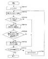
次に、本実施例に係る半導体記憶装置11のエラー検出処理及びリフレッシュ処理の処理動作について、図2及び図4のフローチャートを参照して説明する。 Next, the processing operations of the error detection process and the refresh process of the
コントローラ12は、例えば半導体記憶装置11の電源が投入された直後のタイミングで、NANDフラッシュメモリ13のエラー検出処理を実行する。本実施例のエラー検出処理は、誤り訂正符号ECCを用いた誤り検出訂正処理であり、n個のブロックの各々についてページ毎に行われる。以下の説明では、NANDフラッシュメモリ13のn個のブロックを第1ブロック〜第nブロック、m個のページを第1ページ〜第mページとする。 The
コントローラ12は、NANDフラッシュメモリ13のn個のブロックのうち、エラー検出の対象となるブロックを示す“k”の値をk=1にセットする(STEP101)。 The
コントローラ12は、NANDフラッシュメモリ13の第kブロックを対象としてデータ検査を実行する(STEP102)。具体的には、第1〜第mページの各々から順次データを読み出し、読み出したデータに対して誤り検出訂正を行うことにより、各ページのデータの劣化の有無を検出する。 The
コントローラ12は、データ検査(誤り検出訂正処理)の結果、データの劣化したページが発見されたか否かを判定する(STEP103)。 The
データの劣化したページが発見されたと判定すると(STEP103:Yes)、コントローラ12は、誤り訂正を経たNANDフラッシュメモリ13の当該ページのデータを、冗長メモリ15に書き込む(STEP104)。一方、データの劣化したページが発見されたと判定されなかった場合(STEP103:No)、STEP107に進む。 When it is determined that a page with deteriorated data is found (STEP103: Yes), the
図3は、STEP104で行われる冗長メモリへのデータの書き込みを模式的に示す図である。例えば、NANDフラッシュメモリ13の「ブロック2」の「ページ1」でデータの劣化が検出された場合、ブロック2のページ1(図4に斜線で示す)に記録されていたデータである「データ2,1」が誤り訂正を経て冗長メモリ15に書き込まれる。 FIG. 3 is a diagram schematically showing the writing of data to the redundant memory performed in STEP 104. For example, when data deterioration is detected on "Page 1" of "Block 2" of the
再び図2を参照すると、コントローラ12は、第kブロックの閾値以上のページ数のデータが冗長メモリ15に格納されたか否か(すなわち、第kブロックの所定以上のデータ量のデータが冗長メモリ15に書き込まれたか否か)を判定する(STEP105)。 Referring to FIG. 2 again, the
第kブロックの閾値以上のページ数のデータが冗長メモリ15に格納されたと判定すると(STEP105:Yes)、コントローラ12は、NANDフラッシュメモリ13のリフレッシュ処理を実行する(STEP106)。 When it is determined that the data of the number of pages equal to or greater than the threshold value of the kth block is stored in the redundant memory 15 (STEP 105: Yes), the
図4は、リフレッシュ処理の処理ルーチンを示すフローチャートである。まず、コントローラ12は、リフレッシュ処理におけるデータの書き込み先として用いるブロック(以下、リフレッシュ先ブロックと称する)を空きブロックとするため、当該ブロックに書き込まれているデータを消去する(STEP201)。 FIG. 4 is a flowchart showing a processing routine of refresh processing. First, the
コントローラ12は、NANDフラッシュメモリ13の第kブロックのm個のページのうち、リフレッシュ処理におけるデータ移動の対象となるページを示す“j”の値をj=1にセットする(STEP202)。 The
コントローラ12は、jページ目のデータが冗長メモリ15に格納されているか否か、すなわち図2のフローチャートのSTEP104で冗長メモリ15に書き込まれたデータであるか否かを判定する(STEP203)。 The
jページ目のデータが冗長メモリ15に格納されていると判定すると(STEP203:Yes)、コントローラ12は、jページ目のデータを冗長メモリ15から読み出す(STEP204)。 When it is determined that the data on the j-th page is stored in the redundant memory 15 (STEP203: Yes), the
一方、jページ目のデータが冗長メモリ15に格納されていないと判定すると(STEP203:No)、コントローラ12は、jページ目のデータをNANDフラッシュメモリ13の第kブロックの第jページから読み出す(STEP205)。 On the other hand, if it is determined that the data on the jth page is not stored in the redundant memory 15 (STEP203: No), the
コントローラ12は、STEP204又はSTEP205で読み出されたjページ目のデータを、NANDフラッシュメモリ13のリフレッシュ先ブロックのメモリ領域に書き込む(STEP206)。 The
図5は、STEP204〜206で行われるデータの読み出し及び書き込みを模式的に示す図である。ここでは、NANDフラッシュメモリ13の「ブロック2」を対象とするエラー検出処理(図2のSTEP102〜104を参照)において、「ページ1、3、4、5及びm」でデータのエラーが検出された場合を例として示している。 FIG. 5 is a diagram schematically showing reading and writing of data performed in STEP 204 to 206. Here, in the error detection process for the "block 2" of the NAND flash memory 13 (see STEP 102 to 104 in FIG. 2), a data error is detected on "pages 1, 3, 4, 5 and m". The case is shown as an example.
ページ1、3、4、5及びmでデータのエラーが検出された場合、当該ページに記憶されていたデータが誤り訂正を経て冗長メモリ15にコピーされる。このため、図5に示すように、冗長メモリ15には、NANDフラッシュメモリ13のブロック2のページ1、3、4、5及びmの各々に対応するデータである「データ2,1」、「データ2,3」、「データ2,4」、「データ2,5」及び「データ2,m」が格納されている。従って、コントローラ12は、これらのデータを読み出し、リフレッシュ先のブロックである「ブロックX」に書き込む。 When a data error is detected on pages 1, 3, 4, 5 and m, the data stored on the page is copied to the
一方、ブロック2のページ1、3、4、5及びm以外のページに書き込まれているデータについては、データエラーが検出されていないため、対応するデータが冗長メモリ15に格納されていない。このため、コントローラ12は、これらのデータをNANDフラッシュメモリ13のブロック2から読み出し、リフレッシュ先のブロックであるブロックXに書き込む。 On the other hand, for the data written on the pages other than pages 1, 3, 4, 5 and m of the block 2, since no data error is detected, the corresponding data is not stored in the
これにより、ブロックXには、ページ1〜mに対応するデータ2,1、データ2,2データ2,3、・・・データ2,mが書き込まれ、ブロック2についてのリフレッシュ処理が完了する。 As a result, data 2, 1, data 2, 2 data 2, 3, ... Data 2, m corresponding to pages 1 to m are written in the block X, and the refresh process for the block 2 is completed.
再び図4を参照すると、コントローラ12は、STEP203〜206の一連の処理が第kブロックのmページ目まで行われたか否かを判定する(STEP207)。 With reference to FIG. 4 again, the
一連の処理がmページ目まで行われていないと判定すると(STEP207:No)、jの値を“+1”だけインクリメントし(STEP208)、STEP203に戻る。 If it is determined that the series of processes has not been performed up to the mth page (STEP207: No), the value of j is incremented by "+1" (STEP208), and the process returns to STEP203.
一方、一連の処理がmページ目まで行われたと判定すると(STEP207:Yes)、冗長メモリ15に記録されている第kブロックのデータを消去し(STEP209)、リフレッシュ処理を終了する。 On the other hand, when it is determined that the series of processes has been performed up to the mth page (STEP207: Yes), the data of the kth block recorded in the
再び図2を参照すると、STEP103においてデータの劣化したページが発見されたと判定されなかった場合(STEP103:No)、STEP105において第kブロックの閾値以上のページ数のデータが冗長メモリ15に格納されていないと判定された場合(STEP105:No)、及びSTEP106の第kブロックのリフレッシュ処理が終了した場合、コントローラ12は、STEP102〜106の一連の処理が第nブロックまで行われたか否かを判定する(STEP107)。 Referring to FIG. 2 again, when it is not determined in STEP103 that a page with deteriorated data is found (STEP103: No), the
一連の処理が第nブロックまで行われていないと判定すると(STEP107:No)、kの値を“+1”だけインクリメントし(STEP108)、STEP102に戻る。 If it is determined that the series of processes has not been performed up to the nth block (STEP107: No), the value of k is incremented by "+1" (STEP108), and the process returns to STEP102.
一方、一連の処理が第nブロックまで行われたと判定すると(STEP107:Yes)、NANDフラッシュメモリ13についてのエラー検出処理を終了する。 On the other hand, when it is determined that the series of processes has been performed up to the nth block (STEP107: Yes), the error detection process for the
以上のように、本実施例の半導体記憶装置11では、NANDフラッシュメモリ13からデータを読み出して誤り検出訂正を行い、エラーが検出されたページのデータを冗長メモリ15に書き込む。そして、特定のブロック内の一定以上のページ数のデータが冗長メモリ15に記録された場合に、当該ブロックのリフレッシュ処理を実行する。 As described above, in the
本実施例の半導体記憶装置11によれば、データの劣化が発見されたページの数が1つのブロックにつき所定数以上に達した場合に当該ブロックのリフレッシュ処理を行うため、データが劣化したページが発見される度にリフレッシュ処理を行う場合と比べて、データの消去回数を抑えることができる。従って、NANDフラッシュメモリ13を長寿命化することが可能となる。 According to the
次に、本発明の実施例2について説明する。図6は、本実施例のNANDフラッシュ制御システム200の概略構成を示すブロック図である。NANDフラッシュ制御システム200は、ホストコンピュータ20及び半導体記憶装置21から構成されている。 Next, Example 2 of the present invention will be described. FIG. 6 is a block diagram showing a schematic configuration of the NAND
半導体記憶装置21は、コントローラ12、RAM14及びNANDフラッシュメモリ23を有する。 The semiconductor storage device 21 includes a
本実施例のNANDフラッシュメモリ23は、複数のブロックからなる第1の領域と、これとは異なるブロックからなる第2の領域と、から構成されている。 The
第1の領域は、NANDフラッシュメモリ23に対する通常のデータの書き込みに用いられるメモリ領域である。第1の領域は、各々がm個のページからなるp個のブロック(pはp<nを満たす自然数)から構成されている。本実施例では、第1の領域へのデータの書き込みはMLC方式によって行われる。 The first area is a memory area used for writing ordinary data to the
第2の領域は、第1の領域においてデータが劣化したページが検出された場合に、当該ページのデータを書き込むためのメモリ領域である。すなわち、本実施例では、実施例1の冗長メモリ15(図1を参照)の代わりに、通常のメモリ領域として用いる第1の領域と同一のチップ内に、冗長領域として用いる第2の領域が設けられている。第2の領域は、各々がr個のページ(rはr<mを満たす自然数)からなるq個のブロック(qはq=n−pを満たす自然数)から構成されている。本実施例では、第2の領域へのデータの書き込みはSLC方式によって行われる。 The second area is a memory area for writing the data of the page when a page whose data has deteriorated is detected in the first area. That is, in this embodiment, instead of the redundant memory 15 (see FIG. 1) of the first embodiment, a second area used as the redundant area is provided in the same chip as the first area used as the normal memory area. It is provided. The second region is composed of q blocks (q is a natural number satisfying q = n−p), each consisting of r pages (r is a natural number satisfying r <m). In this embodiment, the writing of data to the second region is performed by the SLC method.
コントローラ12は、NANDフラッシュメモリ13の第1の領域のp個のブロックに対してページ毎に誤り検出訂正処理を行い、各ページにおけるデータの劣化の有無を検出する。データの劣化したページを発見すると、コントローラ12は、誤り訂正を経た当該ページのデータをNANDフラッシュメモリ13の第2の領域に書き込む。 The
図7は、第2の領域へのデータの書き込みを模式的に示す図である。例えば、NANDフラッシュメモリ13の第1の領域のブロック2において、ページ1、3及び4でデータの劣化が検出された場合、これらのページに記録されていたデータである「データ2,1」、「データ2,3」及び「データ2,4」が誤り訂正を経てNANDフラッシュメモリ13の第2の領域に書き込まれる。以後、ブロックのリフレッシュ処理が行われるまでの間、当該ページのデータを読み出す際には、第2の領域からデータの読み出しが行われる。そして、第1の領域のブロックのリフレッシュ処理が行われると、当該ブロックに対応するデータは第2の領域から消去される。 FIG. 7 is a diagram schematically showing the writing of data to the second region. For example, when data deterioration is detected on pages 1, 3 and 4 in the block 2 of the first area of the
なお、第2の領域の1つのブロックには第1の領域の1つのブロックのページのデータが書き込まれるように、管理及び制御がなされる。すなわち、第1の領域の同一のブロックに記録されていたデータは、第2の領域の同一のブロックに書き込まれる。そして、第1の領域の互いに異なるブロックに記録されていたデータは、第2の領域の互いに異なるブロックにそれぞれ書き込まれる。 It should be noted that management and control are performed so that the page data of one block of the first area is written in one block of the second area. That is, the data recorded in the same block in the first area is written in the same block in the second area. Then, the data recorded in the different blocks of the first region are written in the different blocks of the second region.
コントローラ12は、第2の領域の1つのブロックの全ページ(すなわち、r個のページ)にデータが書き込まれた場合に、そのデータの元の記録場所であるページを含む第1の領域のブロックについて、リフレッシュ処理を実行する。 When data is written to all pages (that is, r pages) of one block of the second region, the
リフレッシュ処理では、コントローラ12は、第2の領域に記録されているデータ(すなわち、データの劣化が発見されたページのデータ)については、第2の領域から読み出したデータをリフレッシュ先のブロックに書き込む。一方、第2の領域に記録されていないデータ(すなわち、データの劣化が発見されなかったページのデータ)については、コントローラ12は、第1の領域から読み出したデータをリフレッシュ先のブロックに書き込む。 In the refresh process, the
このように、本実施例の半導体記憶装置21では、NANDフラッシュメモリ13にSLC方式でデータを書き込む第2の領域を設け、データエラーが検出されたページのデータの移動先となる退避用のメモリとして使用する。SLC方式は、MLC方式やTLC方式と比べてデータの消去可能回数が多いため、データが繰り返し消去されることを前提とする退避用のメモリとして使用しても、NANDフラッシュメモリ13の寿命の低下を抑えることができる。従って、本実施例の半導体記憶装置21によれば、実施例1のような冗長メモリを別途設けることなく、NANDフラッシュメモリ13を長寿命化することが可能となる。 As described above, in the semiconductor storage device 21 of the present embodiment, the
なお、本発明は上記実施例で示したものに限られない。例えば、上記実施例では、半導体記憶装置11の電源投入の直後にNANDフラッシュメモリ13の第1〜第nのブロックの各々のページについて順次エラー検出処理を行う例について説明した。しかし、エラー検出処理を行うタイミングはこれに限られない。例えば、あるブロックに対してアクセスがあった場合に、そのブロックについてのみエラー検出処理を行ってもよい。この場合、当該ブロックのみを対象として、図2のフローチャートのSTEP103〜106の処理(すなわち、冗長メモリ15へのデータの書き込み及びリフレッシュ処理)が実行される。 The present invention is not limited to that shown in the above examples. For example, in the above embodiment, an example in which error detection processing is sequentially performed for each page of the first to nth blocks of the
また、電源投入直後にエラー検出処理を行う場合であっても、必ずしも1回のエラー検出処理で全てのブロックに対して処理を行わなくてもよい。例えば、1回の電源投入につきk個(kはn未満の自然数)のブロックを対象としてエラー検出処理を行い、対象となるブロックを電源投入毎に順次遷移させるようにしてもよい。 Further, even when the error detection process is performed immediately after the power is turned on, it is not always necessary to perform the process for all the blocks in one error detection process. For example, error detection processing may be performed on k blocks (k is a natural number less than n) for each power-on, and the target blocks may be sequentially transitioned each time the power is turned on.
また、上記実施例2では、NANDフラッシュメモリ23が、通常のデータの書き込みを行う第1の領域と、エラーを含むページが検出された際に当該ページのデータの書き込みを行う第2の領域と、から構成されている場合について説明した。しかし、第1の領域及び第2の領域の区分は、予めなされていなくてもよい。すなわち、通常の状態ではNANDフラッシュメモリ23の全てのメモリ領域を第1の領域として使用し、データの劣化が検出された場合に、その時点で空いているブロックを第2の領域として使用するように構成されていてもよい。 Further, in the second embodiment, the
また、上記実施例2では、MLC方式で第1の領域へのデータの書き込みを行い、SLC方式で第2の領域へのデータの書き込みを行う場合を例として説明した。しかし、データ記録方式はこれに限られない。例えば、第1の領域にはTLC(Triple Level Cell)方式でデータを記録し、第2の領域にはMLC方式でデータを記録するようにしてもよい。ただし、第2の領域は、データエラーが検出された第1の領域のページのデータを一時的に移す退避用のメモリとして用いる領域であり、繰り返し消去が行われることを前提とする記憶領域であるため、第1の領域よりも消去可能回数の多いデータ記録方式を採用することが望ましい。 Further, in the second embodiment, a case where data is written to the first area by the MLC method and data is written to the second area by the SLC method will be described as an example. However, the data recording method is not limited to this. For example, data may be recorded in the first area by the TLC (Triple Level Cell) method, and data may be recorded in the second area by the MLC method. However, the second area is an area used as a memory for saving the page data of the first area in which a data error is detected temporarily, and is a storage area on the premise that repeated erasure is performed. Therefore, it is desirable to adopt a data recording method in which the number of erasable times is larger than that in the first area.
また、上記実施例では、リフレッシュ処理の最初の段階(図4のSTEP201)でリフレッシュ先ブロックに書き込まれているデータを消去する場合を例として説明した。しかし、リフレッシュ先ブロックのデータの消去のタイミングはこれに限られず、リフレッシュ処理を行う段階でリフレッシュ先ブロックにデータが記録されていない状態が実現されていればよい。例えば、予め空きブロックとなっているブロックをリフレッシュ先ブロックとして用いてもよい。また、リフレッシュ処理を行った後に元のデータが記録されていたブロックの消去を行うことにより、一定の空きブロックが常に確保されるようにしてもよい。 Further, in the above embodiment, the case where the data written in the refresh destination block is deleted in the first stage of the refresh process (STEP201 in FIG. 4) has been described as an example. However, the timing of erasing the data in the refresh destination block is not limited to this, and it is sufficient that the state in which the data is not recorded in the refresh destination block is realized at the stage of performing the refresh process. For example, a block that has been vacant in advance may be used as the refresh destination block. Further, a certain free block may be always secured by erasing the block in which the original data was recorded after the refresh process is performed.
また、上記実施例2では、第2の領域の1つのブロックの全ページにデータが格納された場合にリフレッシュ処理を行う場合を例として説明した。しかし、リフレッシュ処理を行わず、エラー検出時のデータの移動先(退避先)である第2領域のブロックを、そのままデータのコピー先のブロックとして用いてもよい。例えば、図8に示すように、劣化したデータを含むページを発見した際に当該ページのデータを第2の領域のブロックに順次書き込み、第2の領域の1のブロックの全てのページにデータが格納された場合には、当該1のブロックに隣接するブロックにデータを順次書き込む。第2の領域の複数のブロックに亘ってデータを記録することにより、最終的には第1の領域の1のブロックの全てのページのデータを第2領域に移すことができる。そして、第1の領域の1のブロックに対応するデータを第2の領域の複数のブロックで管理することにより、リフレッシュ処理を行うことなくデータの書き直しを完了することができる。従って、リフレッシュ処理に付随するデータの消去を行う必要がないため、NANDフラッシュメモリを長寿命化することが可能となる。 Further, in the second embodiment, a case where the refresh process is performed when the data is stored in all the pages of one block of the second area has been described as an example. However, the block of the second region, which is the data movement destination (save destination) at the time of error detection, may be used as it is as the data copy destination block without performing the refresh process. For example, as shown in FIG. 8, when a page containing deteriorated data is found, the data of the page is sequentially written to the blocks of the second area, and the data is stored in all the pages of the block 1 of the second area. When it is stored, the data is sequentially written in the block adjacent to the block 1. By recording data over a plurality of blocks in the second region, it is possible to finally transfer the data of all pages of one block in the first region to the second region. Then, by managing the data corresponding to one block in the first area in the plurality of blocks in the second area, the rewriting of the data can be completed without performing the refresh process. Therefore, it is not necessary to erase the data associated with the refresh process, so that the life of the NAND flash memory can be extended.
また、本発明の半導体記憶装置は、NANDフラッシュメモリ以外の他の種類の不揮発性メモリにも適用することが可能である。例えば、NANDフラッシュメモリはページ毎にデータの書き込み及び読み出しを行い、ブロック毎にデータの消去を行うことを前提としているが、これとは異なり、ページ毎にデータの消去を行うことが可能な不揮発性メモリに本発明を適用することも可能である。このような不揮発性メモリにおいても、誤りを含むページの数が一定以上に達した場合にリフレッシュ処理を実行することにより、その都度リフレッシュ処理を実行する場合と比べて、少ない機会に集中してリフレッシュ処理を行うことが可能となる。 Further, the semiconductor storage device of the present invention can be applied to other types of non-volatile memory other than NAND flash memory. For example, NAND flash memory is premised on writing and reading data on a page-by-page basis and erasing data on a block-by-block basis, but unlike this, non-volatile data can be erased on a page-by-page basis. It is also possible to apply the present invention to sex memory. Even in such a non-volatile memory, by executing the refresh process when the number of pages containing errors reaches a certain level or more, the refresh process is concentrated on fewer opportunities than when the refresh process is executed each time. It becomes possible to perform processing.
100、200 NANDフラッシュ制御システム
10 ホストコンピュータ
11、21 半導体記憶装置
12 コントローラ
13 NANDフラッシュメモリ
14 RAM
15 冗長メモリ100, 200 NAND
15 Redundant memory
Claims (10)
Translated fromJapanese複数のセルを有する第2の記憶部と、
前記第1の記憶部及び前記第2の記憶部に対するデータの書き込み、読み出し及び消去を制御する制御部と、
を有し、
前記制御部は、前記第1の記憶部からページ毎にデータを読み出して誤り検出を行い、
当該誤り検出において、前記第1の記憶部内でデータの誤りを含むページが検出された場合には、当該誤りを含むページのデータに誤り訂正を施したデータを前記第2の記憶部に書き込み、
前記第1の記憶部の1のブロック内の所定数のページに記憶されていたデータが前記第2の記憶部に書き込まれた場合に、前記1のブロックのリフレッシュ処理を実行することを特徴とする半導体記憶装置。A first storage unit having n blocks (m and n are integers of 2 or more), each containing m pages consisting of a plurality of cells.
A second storage unit having multiple cells,
A control unit that controls writing, reading, and erasing of data to the first storage unit and the second storage unit.
Have,
The control unit reads data page by page from the first storage unit, performs error detection, and performs error detection.
In the error detection, when a page containing a data error is detected in the first storage unit, the data of the page containing the error is error-corrected and the data is written to the second storage unit.
When the data stored in a predetermined number of pages in one block of the first storage unit is written to the second storage unit, the refresh process of the first block is executed. Semiconductor storage device.
セル毎に記録されるデータのビット数が前記第1のデータ記録方式よりも少ない第2のデータ記録方式で前記第2の記憶部にデータを書き込むことを特徴とする請求項1乃至3のいずれか1に記載の半導体記憶装置。The control unit writes data to the first storage unit by the first data recording method, which is a method of recording data of a plurality of bits for each cell.
7. The semiconductor storage device according to 1.
前記第2のデータ記録方式は、SLC(Single Level Cell)方式であることを特徴とする請求項4に記載の半導体記憶装置。The first data recording method is an MLC (Multiple Level Cell) method or a TLC (Triple Level Cell) method.
The semiconductor storage device according to claim 4, wherein the second data recording method is an SLC (Single Level Cell) method.
前記第2の記憶部は、前記第2のデータ記録方式でデータが記録される第2の不揮発性メモリから構成されていることを特徴とする請求項4又は5に記載の半導体記憶装置。The first storage unit is composed of a first non-volatile memory in which data is recorded by the first data recording method.
The semiconductor storage device according to claim 4 or 5, wherein the second storage unit is composed of a second non-volatile memory in which data is recorded by the second data recording method.
前記第2の記憶部は、前記1の不揮発性メモリ内の前記n個のブロックとは異なるブロックから構成されていることを特徴とする請求項1乃至5のいずれか1に記載の半導体記憶装置。The first storage unit is configured as a block group consisting of n blocks in one non-volatile memory.
The semiconductor storage device according to any one of claims 1 to 5, wherein the second storage unit is composed of blocks different from the n blocks in the non-volatile memory. ..
前記第1の記憶部からページ毎にデータを読み出して誤り検出を行うステップと、
前記誤り検出において前記第1の記憶部にデータの誤りを含むページが検出された場合に、当該誤りを含むページのデータに誤り訂正を施したデータを前記第2の記憶部に書き込むステップと、
前記第1の記憶部の1のブロックの所定数のページに記憶されていたデータが前記第2の記憶部に書き込まれた場合に、前記1のブロックのリフレッシュ処理を実行するステップと、
を含むことを特徴とするリフレッシュ方法。A first storage unit having n blocks (m and n are integers of 2 or more) each containing m pages each consisting of a plurality of cells, a second storage unit having a plurality of cells, and data. It is a block refreshing method executed by a semiconductor storage device having a control unit for controlling writing, reading, erasing, and error detection / correction processing.
A step of reading data page by page from the first storage unit and performing error detection, and
When a page containing a data error is detected in the first storage unit in the error detection, a step of writing error-corrected data to the second storage unit in the data of the page containing the error, and
A step of executing a refresh process of the first block when data stored in a predetermined number of pages of one block of the first storage unit is written to the second storage unit.
A refreshing method characterized by including.
前記1のブロックのm個のページに記憶されているデータのうち、前記第2の記憶部に書き込まれた前記データを前記第1の記憶部の1の空きブロックに書き込むステップと、
前記1のブロックのm個のページに記憶されているデータのうち、前記第2の記憶部に書き込まれた前記データ以外のデータを前記第1の記憶部の前記1のブロックから読み出して前記1の空きブロックに書き込むステップと、
を含むことを特徴とする請求項8に記載のリフレッシュ方法。The step of executing the refresh process is
A step of writing the data written in the second storage unit to one empty block of the first storage unit among the data stored in m pages of the first block, and a step of writing the data written in the second storage unit.
Of the data stored in the m pages of the 1 block, data other than the data written in the 2nd storage unit is read from the 1 block of the 1st storage unit, and the 1st block is read. Steps to write to an empty block of
The refreshing method according to claim 8, wherein the refreshing method comprises.
Priority Applications (1)
| Application Number | Priority Date | Filing Date | Title |
|---|---|---|---|
| JP2020009681AJP7291640B2 (en) | 2020-01-24 | 2020-01-24 | Semiconductor memory device and refresh method for semiconductor memory device |
Applications Claiming Priority (1)
| Application Number | Priority Date | Filing Date | Title |
|---|---|---|---|
| JP2020009681AJP7291640B2 (en) | 2020-01-24 | 2020-01-24 | Semiconductor memory device and refresh method for semiconductor memory device |
Publications (2)
| Publication Number | Publication Date |
|---|---|
| JP2021118011Atrue JP2021118011A (en) | 2021-08-10 |
| JP7291640B2 JP7291640B2 (en) | 2023-06-15 |
Family
ID=77175092
Family Applications (1)
| Application Number | Title | Priority Date | Filing Date |
|---|---|---|---|
| JP2020009681AActiveJP7291640B2 (en) | 2020-01-24 | 2020-01-24 | Semiconductor memory device and refresh method for semiconductor memory device |
Country Status (1)
| Country | Link |
|---|---|
| JP (1) | JP7291640B2 (en) |
Citations (3)
| Publication number | Priority date | Publication date | Assignee | Title |
|---|---|---|---|---|
| JP2004326867A (en)* | 2003-04-22 | 2004-11-18 | Toshiba Corp | Data storage system |
| JP2005243183A (en)* | 2004-02-27 | 2005-09-08 | Toshiba Corp | Data storage system |
| JP2009205578A (en)* | 2008-02-29 | 2009-09-10 | Toshiba Corp | Semiconductor storage device |
- 2020
- 2020-01-24JPJP2020009681Apatent/JP7291640B2/enactiveActive
Patent Citations (3)
| Publication number | Priority date | Publication date | Assignee | Title |
|---|---|---|---|---|
| JP2004326867A (en)* | 2003-04-22 | 2004-11-18 | Toshiba Corp | Data storage system |
| JP2005243183A (en)* | 2004-02-27 | 2005-09-08 | Toshiba Corp | Data storage system |
| JP2009205578A (en)* | 2008-02-29 | 2009-09-10 | Toshiba Corp | Semiconductor storage device |
Also Published As
| Publication number | Publication date |
|---|---|
| JP7291640B2 (en) | 2023-06-15 |
Similar Documents
| Publication | Publication Date | Title |
|---|---|---|
| CN103853582B (en) | flash memory updating method | |
| US7477547B2 (en) | Flash memory refresh techniques triggered by controlled scrub data reads | |
| US8271515B2 (en) | System and method for providing copyback data integrity in a non-volatile memory system | |
| US7573773B2 (en) | Flash memory with data refresh triggered by controlled scrub data reads | |
| US9189313B2 (en) | Memory system having NAND-type flash memory and memory controller with shift read controller and threshold voltage comparison module | |
| KR101103110B1 (en) | Memory system | |
| US8760921B2 (en) | Storage device and control method of nonvolatile memory | |
| TWI388982B (en) | Semiconductor memory device with memory cell having charge accumulation layer and control gate and memory system | |
| KR101468432B1 (en) | Flash memory refresh techniques triggered by controlled scrub data reads | |
| US20170162267A1 (en) | Data Storage Device and Data Maintenance Method | |
| US20190065361A1 (en) | Method for writing data into flash memory module and associated flash memory controller and electronic device | |
| US11656790B2 (en) | Memory system, memory controller, and operation method of memory system | |
| US11487655B2 (en) | Method for managing flash memory module and associated flash memory controller and electronic device based on timing of dummy read operations | |
| JP5494086B2 (en) | Nonvolatile storage device and nonvolatile memory controller | |
| US11249838B2 (en) | Memory system, memory controller, and method of operating memory controller | |
| US11210209B2 (en) | Method for managing flash memory module and associated flash memory controller and electronic device | |
| US20210034541A1 (en) | Memory system, memory control device, and memory control method | |
| JP2021140311A (en) | Memory system | |
| JP7291640B2 (en) | Semiconductor memory device and refresh method for semiconductor memory device | |
| US8885406B2 (en) | Memory device, memory control device, and memory control method | |
| US20120311243A1 (en) | Method for increasing reliability of data accessing for a multi-level cell type non-volatile memory | |
| US11809748B2 (en) | Control method of flash memory controller and associated flash memory controller and electronic device | |
| US12197770B2 (en) | Memory system, memory controller, and operation method of memory system | |
| US20240012569A1 (en) | Storage controller receiving read data and distribution information, method of operating the same, and method of operating storage device including the same | |
| JP2009211188A (en) | Memory system |
Legal Events
| Date | Code | Title | Description |
|---|---|---|---|
| A621 | Written request for application examination | Free format text:JAPANESE INTERMEDIATE CODE: A621 Effective date:20220907 | |
| TRDD | Decision of grant or rejection written | ||
| A977 | Report on retrieval | Free format text:JAPANESE INTERMEDIATE CODE: A971007 Effective date:20230428 | |
| A01 | Written decision to grant a patent or to grant a registration (utility model) | Free format text:JAPANESE INTERMEDIATE CODE: A01 Effective date:20230509 | |
| A61 | First payment of annual fees (during grant procedure) | Free format text:JAPANESE INTERMEDIATE CODE: A61 Effective date:20230605 | |
| R150 | Certificate of patent or registration of utility model | Ref document number:7291640 Country of ref document:JP Free format text:JAPANESE INTERMEDIATE CODE: R150 |