JP2021111813A - Power supply circuit for circularly polarized antenna - Google Patents
Power supply circuit for circularly polarized antennaDownload PDFInfo
- Publication number
- JP2021111813A JP2021111813AJP2020000527AJP2020000527AJP2021111813AJP 2021111813 AJP2021111813 AJP 2021111813AJP 2020000527 AJP2020000527 AJP 2020000527AJP 2020000527 AJP2020000527 AJP 2020000527AJP 2021111813 AJP2021111813 AJP 2021111813A
- Authority
- JP
- Japan
- Prior art keywords
- circuit
- feeding
- phase shift
- circularly polarized
- polarized antenna
- Prior art date
- Legal status (The legal status is an assumption and is not a legal conclusion. Google has not performed a legal analysis and makes no representation as to the accuracy of the status listed.)
- Granted
Links
Images


Classifications
- H—ELECTRICITY
- H01—ELECTRIC ELEMENTS
- H01P—WAVEGUIDES; RESONATORS, LINES, OR OTHER DEVICES OF THE WAVEGUIDE TYPE
- H01P1/00—Auxiliary devices
- H01P1/165—Auxiliary devices for rotating the plane of polarisation
- H01P1/17—Auxiliary devices for rotating the plane of polarisation for producing a continuously rotating polarisation, e.g. circular polarisation
- H—ELECTRICITY
- H01—ELECTRIC ELEMENTS
- H01P—WAVEGUIDES; RESONATORS, LINES, OR OTHER DEVICES OF THE WAVEGUIDE TYPE
- H01P5/00—Coupling devices of the waveguide type
- H01P5/12—Coupling devices having more than two ports
- H01P5/16—Conjugate devices, i.e. devices having at least one port decoupled from one other port
- H—ELECTRICITY
- H01—ELECTRIC ELEMENTS
- H01Q—ANTENNAS, i.e. RADIO AERIALS
- H01Q15/00—Devices for reflection, refraction, diffraction or polarisation of waves radiated from an antenna, e.g. quasi-optical devices
- H01Q15/24—Polarising devices; Polarisation filters
- H01Q15/242—Polarisation converters
- H01Q15/244—Polarisation converters converting a linear polarised wave into a circular polarised wave
- H—ELECTRICITY
- H01—ELECTRIC ELEMENTS
- H01Q—ANTENNAS, i.e. RADIO AERIALS
- H01Q9/00—Electrically-short antennas having dimensions not more than twice the operating wavelength and consisting of conductive active radiating elements
- H01Q9/04—Resonant antennas
- H01Q9/0407—Substantially flat resonant element parallel to ground plane, e.g. patch antenna
- H01Q9/0428—Substantially flat resonant element parallel to ground plane, e.g. patch antenna radiating a circular polarised wave
- H—ELECTRICITY
- H03—ELECTRONIC CIRCUITRY
- H03F—AMPLIFIERS
- H03F3/00—Amplifiers with only discharge tubes or only semiconductor devices as amplifying elements
- H03F3/60—Amplifiers in which coupling networks have distributed constants, e.g. with waveguide resonators
- H—ELECTRICITY
- H03—ELECTRONIC CIRCUITRY
- H03H—IMPEDANCE NETWORKS, e.g. RESONANT CIRCUITS; RESONATORS
- H03H7/00—Multiple-port networks comprising only passive electrical elements as network components
- H03H7/18—Networks for phase shifting
- H03H7/185—Networks for phase shifting comprising distributed impedance elements together with lumped impedance elements
- H—ELECTRICITY
- H03—ELECTRONIC CIRCUITRY
- H03H—IMPEDANCE NETWORKS, e.g. RESONANT CIRCUITS; RESONATORS
- H03H7/00—Multiple-port networks comprising only passive electrical elements as network components
- H03H7/18—Networks for phase shifting
- H03H7/21—Networks for phase shifting providing two or more phase shifted output signals, e.g. n-phase output
- H—ELECTRICITY
- H03—ELECTRONIC CIRCUITRY
- H03H—IMPEDANCE NETWORKS, e.g. RESONANT CIRCUITS; RESONATORS
- H03H7/00—Multiple-port networks comprising only passive electrical elements as network components
- H03H7/48—Networks for connecting several sources or loads, working on the same frequency or frequency band, to a common load or source
- H—ELECTRICITY
- H04—ELECTRIC COMMUNICATION TECHNIQUE
- H04B—TRANSMISSION
- H04B1/00—Details of transmission systems, not covered by a single one of groups H04B3/00 - H04B13/00; Details of transmission systems not characterised by the medium used for transmission
- H04B1/06—Receivers
- H04B1/16—Circuits
- H04B1/18—Input circuits, e.g. for coupling to an antenna or a transmission line
Landscapes
- Engineering & Computer Science (AREA)
- Computer Networks & Wireless Communication (AREA)
- Signal Processing (AREA)
- Power Engineering (AREA)
- Variable-Direction Aerials And Aerial Arrays (AREA)
- Waveguide Aerials (AREA)
Abstract
Translated fromJapaneseDescription
Translated fromJapanese本発明は円偏波アンテナ用給電回路に関し、特に、2点給電のパッチアンテナに適した円偏波アンテナ用給電回路に関する。 The present invention relates to a feeding circuit for a circularly polarized antenna, and more particularly to a feeding circuit for a circularly polarized antenna suitable for a patch antenna of two-point feeding.
一般に、円偏波アンテナ、具体的には、円偏波に対応するパッチアンテナは、GNSS(Global Navigation Satellite System:衛星測位システム)用アンテナ等で広く用いられている。円偏波アンテナは、放射素子と地導体の間にセラミックや誘電体基板等が介在して構成されるパッチアンテナが知られている。円偏波アンテナには、1点給電のものや2点給電のものがある。 In general, circularly polarized antennas, specifically, patch antennas corresponding to circularly polarized waves, are widely used in GNSS (Global Navigation Satellite System) antennas and the like. As a circularly polarized antenna, a patch antenna in which a ceramic or a dielectric substrate is interposed between a radiating element and a ground conductor is known. Circularly polarized antennas include those fed at one point and those fed at two points.
ここで、2点給電の円偏波アンテナの場合、それぞれに給電する信号の位相差が90度となるように給電することで、円偏波に対応可能となる。このような位相差を持った給電回路としては、例えば特許文献1に開示のものがある。特許文献1に開示のものは、入力端子にウィルキンソン回路が接続され、2つに分配された信号をそれぞれ出力する出力端子の一方に、90度の位相遅れ回路を1つ用いた位相シフト部が接続され、90度の位相差となるような2つの経路が2点給電の給電点に接続されるものである。 Here, in the case of a circularly polarized antenna fed at two points, it is possible to deal with circularly polarized waves by feeding the signals so that the phase difference of the signals fed to each antenna is 90 degrees. As a feeding circuit having such a phase difference, for example, there is one disclosed in
しかしながら、特許文献1に開示のものは、2つの出力端子の一方の経路のみに位相シフト部が接続された上で2点給電の給電点に接続されるものであるため、位相シフト回路が接続されていない経路と比べて、位相シフト回路がある分、僅かであるが振幅が減衰してしまう問題があった。また、位相シフト回路は、特定の周波数帯域において90度の位相差が得られると共に振幅の減衰量が最小となるように設定された回路である。ここで、給電回路の90度の位相差が得られる周波数帯域や、振幅の減衰量を抑えることが可能な周波数帯域は、比較的狭帯域である。具体的には、GNSSで用いられる周波数帯域のうち、1559MHz−1610MHz(Upper−L Band)の周波数帯域において実用可能な位相差及び振幅比が得られるものであった。 However, in the one disclosed in
近年、GNSS用アンテナでは、上述の1559MHz−1610MHz(Upper−L Band)の周波数帯域に加え、1164MHz−1300MHzの(Lower−L Band)の周波数帯域を含めたGNSSフルバンド対応が求められている。しかしながら、特許文献1に開示のものでは、1164MHz−1300MHzの周波数帯域において実用可能な位相シフト量を得ること、及び振幅の減衰量を抑えることは困難であった。このため、特許文献1に開示の給電回路では、Lower−L BandからUpper−L Bandにわたる広帯域においては、2つの出力端子の位相差が90度からずれてしまい、また、振幅比が大きくなるにしたがって円偏波特性の指標である軸比特性が劣化してしまっていた。 In recent years, GNSS antennas are required to support GNSS full band including the frequency band of 1164 MHz-1300 MHz (Lower-L Band) in addition to the frequency band of 1559 MHz-1610 MHz (Upper-L Band) described above. However, in the case disclosed in
本発明は、斯かる実情に鑑み、円偏波アンテナの2つの給電点に給電するための2つの経路間の位相差を広帯域わたって安定させると共に、振幅比も広帯域にわたって小さい円偏波アンテナ用給電回路を提供しようとするものである。 In view of such circumstances, the present invention is for a circularly polarized antenna in which the phase difference between the two paths for feeding the two feeding points of the circularly polarized antenna is stabilized over a wide band and the amplitude ratio is small over a wide band. It is intended to provide a power supply circuit.
上述した本発明の目的を達成するために、本発明による円偏波アンテナ用給電回路は、入力信号を同相且つ同振幅で2つの経路に分配する合成分配部と、合成分配部により分配される2つの経路と円偏波アンテナの2つの給電点との間にそれぞれ接続される2つの位相シフト回路を有する位相シフト部であって、円偏波アンテナの2つの給電点へ位相差が90度となる信号をそれぞれ出力する位相シフト部と、を具備するものである。 In order to achieve the above-described object of the present invention, the feeding circuit for a circularly polarized antenna according to the present invention is distributed by a composite distribution unit that distributes an input signal into two paths with the same phase and the same amplitude, and a composite distribution unit. It is a phase shift unit having two phase shift circuits connected between two paths and two feeding points of the circularly polarized antenna, and the phase difference is 90 degrees to the two feeding points of the circularly polarized antenna. It is provided with a phase shift unit for outputting each signal.
ここで、位相シフト部は、一方の位相シフト回路が位相遅れ回路からなり、他方の位相シフト回路が位相進み回路からなるものであれば良い。 Here, the phase shift unit may be any one as long as one phase shift circuit is composed of a phase lag circuit and the other phase shift circuit is composed of a phase lead circuit.
また、位相シフト部は、一方の位相シフト回路が−45度位相をシフトし、他方の位相シフト回路が+45度位相をシフトするものであれば良い。 Further, the phase shift unit may be one in which one phase shift circuit shifts the phase by −45 degrees and the other phase shift circuit shifts the phase by +45 degrees.
また、位相シフト部は、一方の位相シフト回路がローパスフィルタ回路構成であり、他方の位相シフト回路がハイパスフィルタ回路構成であれば良い。 Further, in the phase shift unit, one phase shift circuit may have a low-pass filter circuit configuration and the other phase shift circuit may have a high-pass filter circuit configuration.
また、一方の位相シフト回路がCLのL型フィルタ回路、CLCのπ型フィルタ回路、LCLのT型フィルタ回路、又はその多段回路であり、他方の位相シフト回路がLCのL型フィルタ回路、LCLのπ型フィルタ回路、CLCのT型フィルタ回路、又はその多段回路であれば良い。 Further, one phase shift circuit is a CL L-type filter circuit, a CLC π-type filter circuit, an LCL T-type filter circuit, or a multi-stage circuit thereof, and the other phase shift circuit is an LC L-type filter circuit, an LCL. A π-type filter circuit, a CLC T-type filter circuit, or a multi-stage circuit thereof may be used.
また、位相シフト部は、集中定数回路で構成されるものであれば良い。 Further, the phase shift unit may be configured as long as it is composed of a lumped constant circuit.
また、合成分配部は、集中定数回路又は分布定数回路で構成されるウィルキンソン回路からなるものであれば良い。 Further, the composite distribution unit may be a Wilkinson circuit composed of a lumped constant circuit or a distributed constant circuit.
また、4点給電円偏波アンテナに給電するための給電回路は、第1入力端子からの信号を同相且つ同振幅で2つの経路に分配する第1合成分配部と、該第1合成分配部により分配される2つの経路と円偏波アンテナの4つの給電点のうち2つの給電点との間にそれぞれ接続される2つの第1位相シフト回路を有する第1位相シフト部であって、円偏波アンテナの4つの給電点のうち2つの給電点へ位相差が90度となる信号をそれぞれ出力する第1位相シフト部と、からなる第1給電回路と、第2入力端子からの信号を同相且つ同振幅で2つの経路に分配する第2合成分配部と、該第2合成分配部により分配される2つの経路と円偏波アンテナの4つの給電点のうち残りの2つの給電点との間にそれぞれ接続される2つの第2位相シフト回路を有する第2位相シフト部であって、円偏波アンテナの4つの給電点のうち残りの2つの給電点へ位相差が90度となる信号をそれぞれ出力する第2位相シフト部と、からなる第2給電回路と、入力信号を2つの経路に180度の位相差を有するように分配する180度合成分配部であって、180度合成分配部により分配される2つの経路が第1入力端子と第2入力端子にそれぞれ接続され、第1入力端子と第2入力端子へ位相差が180度となる信号をそれぞれ出力する180度合成分配部と、を具備するものであれば良い。 Further, the power feeding circuit for supplying power to the 4-point power feeding circularly polarized antenna includes a first synthetic distribution unit that distributes the signal from the first input terminal to two paths with the same phase and the same amplitude, and the first synthetic distribution unit. A first phase shift unit having two first phase shift circuits connected between two paths distributed by the above and two feed points among the four feed points of the circularly polarized antenna. A first power supply circuit consisting of a first phase shift unit that outputs a signal having a phase difference of 90 degrees to two of the four feeding points of the polarized antenna, and a signal from the second input terminal. The second synthetic distribution section that distributes to two paths with the same phase and the same amplitude, the two paths distributed by the second synthetic distribution section, and the remaining two feeding points of the four feeding points of the circularly polarized antenna. It is a second phase shift part having two second phase shift circuits connected to each other, and the phase difference is 90 degrees to the remaining two feeding points of the four feeding points of the circularly polarized antenna. A 180-degree composite distribution unit that distributes an input signal to two paths so as to have a 180-degree phase difference, and a second power supply circuit consisting of a second phase shift unit that outputs signals, respectively. Two paths distributed by the distribution unit are connected to the first input terminal and the second input terminal, respectively, and 180-degree composite distribution that outputs a signal having a phase difference of 180 degrees to the first input terminal and the second input terminal, respectively. Anything that includes a part and is sufficient.
ここで、180度合成分配部は、入力信号を同相且つ同振幅で2つの経路に分配する第3合成分配部と、第3合成分配部により分配される2つの経路と第1入力端子及び第2入力端子との間にそれぞれ接続される2つの第3位相シフト回路を有する第3位相シフト部と、からなるものであれば良い。 Here, the 180-degree composite distribution unit includes a third composite distribution unit that distributes the input signal to two paths with the same phase and the same amplitude, two paths distributed by the third composite distribution unit, the first input terminal, and the first. It may be composed of a third phase shift unit having two third phase shift circuits connected to each of the two input terminals.
また、180度合成分配部は、180度ラットレース回路からなるものであっても良い。 Further, the 180-degree composite distribution unit may be composed of a 180-degree rat race circuit.
また、180度合成分配部は、入力信号を2つの経路に90度の位相差を有するように分配する90度ハイブリッド回路と、90度ハイブリッド回路により分配される2つの経路の一方の経路に接続される90度位相シフト回路と、からなり、90度位相シフト回路からの経路が第1入力端子に接続され、90度ハイブリッド回路により分配される2つの経路の他方の経路が第2入力端子に接続される、ものであっても良い。 Further, the 180-degree composite distribution unit is connected to one of the two paths distributed by the 90-degree hybrid circuit and the 90-degree hybrid circuit that distributes the input signal to the two paths so as to have a phase difference of 90 degrees. The 90-degree phase shift circuit and the path from the 90-degree phase shift circuit are connected to the first input terminal, and the other path of the two paths distributed by the 90-degree hybrid circuit is connected to the second input terminal. It may be connected.
本発明の円偏波アンテナ用給電回路には、円偏波アンテナの2つの給電点に給電するための2つの経路間の位相差を広帯域わたって安定させると共に、振幅比も広帯域にわたって小さいという利点がある。 The feeding circuit for a circularly polarized antenna of the present invention has an advantage that the phase difference between the two paths for feeding the two feeding points of the circularly polarized antenna is stabilized over a wide band and the amplitude ratio is also small over a wide band. There is.
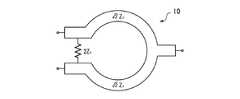
以下、本発明を実施するための形態を図示例と共に説明する。図1は、本発明の円偏波アンテナ用給電回路を説明するための概略ブロック図である。本発明の円偏波アンテナ用給電回路は、円偏波アンテナ1に給電するための給電回路である。なお、図示例の円偏波アンテナ1は、2つの給電点P2,P3から給電される2点給電のパッチアンテナであれば良い。図示の通り、本発明の円偏波アンテナ用給電回路は、合成分配部10と、位相シフト部20とからなる。 Hereinafter, embodiments for carrying out the present invention will be described with reference to the illustrated examples. FIG. 1 is a schematic block diagram for explaining a feeding circuit for a circularly polarized antenna of the present invention. The feeding circuit for a circularly polarized antenna of the present invention is a feeding circuit for feeding the circularly polarized
合成分配部10は、ポートP1からの入力信号を同相且つ同振幅で2つの経路に分配するものである。分配された2つの経路は、後述の位相シフト部20に接続されている。合成分配部10は、集中定数回路や分布定数回路で構成されるものであれば良い。集中定数回路とは、コンデンサやコイルがチップ部品やリード部品等からなるディスクリート部品が用いられる回路である。また、分布定数回路とは、伝送線路により構成されるものや、例えば回路基板上にパターンニングによりコイルやコンデンサが形成されるものである。 The
位相シフト部20は、2つの位相シフト回路21,22を有するものである。2つの位相シフト回路21,22は、合成分配部10により分配される2つの経路と円偏波アンテナ1の2つの給電点P2,P3との間にそれぞれ接続されている。即ち、2つの給電点P2,P3への経路には、それぞれ位相シフト回路21,22が介在する。また、位相シフト回路21,22は、例えば集中定数回路で構成されるものである。即ち、コンデンサやコイルがチップ部品やリード部品等からなるディスクリート部品が用いられれば良い。位相シフト部20は、円偏波アンテナ1の2つの給電点P2,P3へ位相差が90度となる信号をそれぞれ出力するものである。例えば、一方の位相シフト回路21が位相遅れ回路からなり、他方の位相シフト回路22が位相進み回路からなるものであれば良い。例えば、位相シフト回路21が−45度位相をシフトする回路(位相遅れ回路)であれば、位相シフト回路22は+45度位相をシフトする回路(位相進み回路)である。このように、2つの位相シフト回路21,22の位相差(差分)が90度となるものであれば良い。なお、位相シフト部20が位相遅れ回路だけで構成されるものであれば、λ/4の伝送線路等で構成可能である。図示例の円偏波アンテナ用給電回路では、位相シフト部20が位相遅れ回路だけでなく位相進み回路も用いており、集中定数回路で構成されている。なお、これは、コイルやコンデンサをパターンニングで形成した分布定数回路で構成されても良い。また、位相シフト部20が伝送線路による分布定数回路で構成される場合には、例えば位相シフト回路21が−45度位相をシフトする回路(位相遅れ回路)、位相シフト回路22が−135度位相をシフトする回路(位相遅れ回路)というように、両方が位相遅れ回路で構成され、位相差としては90度となるものであっても良い。 The
図2は、本発明の円偏波アンテナ用給電回路を説明するための具体的な回路図である。図中、図1と同一の符号を付した部分は同一物を表している。図示の通り、本発明の円偏波アンテナ用給電回路の合成分配部10は、集中定数回路で構成されるウィルキンソン回路からなるものを示した。図示例のウィルキンソン回路は、位相シフト部20の位相シフト回路21,22へ分配される2つの経路間が抵抗で繋がれる2つのπ型フィルタ回路で構成されている。図示例のπ型フィルタ回路は、具体的にはそれぞれCLCのπ型nローパスフィルタ回路であり、合成分配部10のポートP1と位相シフト部20との間の経路にコイルが直列に接続されると共に、グラウンドに接続された2つのコンデンサがコイルの両端にそれぞれ接続される。なお、ウィルキンソン回路である合成分配部10の並列に接続されるπ型フィルタ回路は、図示例には限定されず、フィルタ回路構成であれば、ローパスフィルタ回路構成であってもハイパスフィルタ回路構成であっても良く、また、L型フィルタ回路やT型フィルタ回路、その多段回路等であっても良い。また、合成分配部10のフィルタ回路の中心周波数は、具体的にはGNSSフルバンド(1164MHz−1610MHz)の通過帯域の中心周波数である例えば1387MHzであれば良い。 FIG. 2 is a specific circuit diagram for explaining the feeding circuit for a circularly polarized antenna of the present invention. In the figure, the parts having the same reference numerals as those in FIG. 1 represent the same objects. As shown in the figure, the combined
また、上述の通り、合成分配部10は、入力信号を同相且つ同振幅で2つの経路に分配可能なものであれば良く、集中定数回路で構成されるものだけでなく、分布定数回路で構成されても良い。図3は、本発明の円偏波アンテナ用給電回路の合成分配部を分布定数回路で構成した場合の一例を説明するための概略平面図である。図示例の合成分配部10は、特性インピーダンスが√2Z0の2本のλ/4伝送線路で分配する形状を有するものであり、位相シフト部20へ分配される2つの伝送線路間が2Z0の抵抗を介して接続されるものである。本発明の円偏波アンテナ用給電回路では、このような分布定数回路で構成される合成分配部を用いても良い。Further, as described above, the
再度図2を参照すると、本発明の円偏波アンテナ用給電回路の位相シフト部20は、一方の位相シフト回路21がローパスフィルタ回路構成であり、他方の位相シフト回路22がハイパスフィルタ回路構成である。図示例の位相シフト回路21は、CLCのπ型フィルタ回路である。具体的には、合成分配部10と給電点P2と間の経路にコイルが接続されると共に、グラウンドに接続された2つのコンデンサがコイルの両端にそれぞれ接続される。また、位相シフト回路22は、LCLのπ型フィルタ回路である。具体的には、合成分配部10と給電点P3との間の経路にコンデンサが直列に接続されると共に、グラウンドに接続された2つのコイルがコンデンサの両端にそれぞれ接続される。 Referring to FIG. 2 again, in the
このように構成されることで、ポートP1からの入力信号が合成分配部10で同相且つ同振幅で分配され、位相シフト部20の位相シフト回路21及び位相シフト回路22にそれぞれ入力され−45度及び+45度に位相をシフトした上で2つの給電点P2,P3へ位相差が90度となる信号がそれぞれ入力される円偏波アンテナ用給電回路となる。 With this configuration, the input signal from the port P1 is distributed by the combined
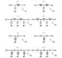
ここで、図4を用いて位相シフト部の他の回路構成の例について説明する。図4は、本発明の円偏波アンテナ用給電回路の位相シフト部の他の回路構成を説明するための回路図である。図中、図1と同一の符号を付した部分は同一物を表している。図4(a)−図4(d)が位相シフト回路21の変形例であり、図4(e)−図4(h)が位相シフト回路22の変形例である。 Here, an example of another circuit configuration of the phase shift unit will be described with reference to FIG. FIG. 4 is a circuit diagram for explaining another circuit configuration of the phase shift portion of the feeding circuit for the circularly polarized antenna of the present invention. In the figure, the parts having the same reference numerals as those in FIG. 1 represent the same objects. 4 (a)-FIG. 4 (d) is a modified example of the
図4(a)に示される通り、位相シフト回路21は、LCのL型フィルタ回路であっても良い。具体的には、合成分配部10と給電点P2との間の経路にコイルが直列に接続されると共に、グラウンドに接続されたコンデンサが給電点P2側に接続される。また、図4(e)に示される通り、位相シフト回路22は、CLのL型フィルタ回路であっても良い。具体的には、合成分配部10と給電点P3との間の経路にコンデンサが直列に接続されると共に、グラウンドに接続されたコイルが給電点P3側に接続される。 As shown in FIG. 4A, the
また、図4(b)に示される通り、位相シフト回路21はLCLのT型フィルタ回路であっても良い。具体的には、合成分配部10と給電点P2との間の経路にコイルが直列に2つ接続されると共に、グラウンドに接続されたコンデンサが2つのコイルの間に接続される。また、図4(f)に示される通り、位相シフト回路22は、CLCのT型フィルタ回路であっても良い。具体的には、合成分配部10と給電点P3との間の経路にコンデンサが直列に2つ接続されると共に、グラウンドに接続されたコイルが2つのコンデンサの間に接続される。 Further, as shown in FIG. 4B, the
また、図4(c)に示される通り、位相シフト回路21はCLCのπ型多段回路であっても良い。具体的には、合成分配部10と給電点P2との間の経路にコイルが直列に2つ接続されると共に、グラウンドに接続された3つのコンデンサが2つのコイル間及び直列のコイルの両端にそれぞれ接続される。また、図4(g)に示される通り、位相シフト回路22は、LCLのπ型多段回路であっても良い。具体的には、合成分配部10と給電点P3との間の経路にコンデンサが直列に2つ接続されると共に、グラウンドに接続された3つのコイルが2つのコンデンサ間及び直列のコンデンサの両端にそれぞれ接続される。 Further, as shown in FIG. 4C, the
また、図4(d)に示される通り、位相シフト回路21はLCLのT型多段回路であっても良い。具体的には、合成分配部10と給電点P2との間の経路にコイルが直列に3つ接続されると共に、グラウンドに接続された2つのコンデンサが3つのコイルの間にそれぞれ接続される。また、図4(h)に示される通り、位相シフト回路22は、CLCのT型多段回路であっても良い。具体的には、合成分配部10と給電点P3との間の経路にコンデンサが直列に3つ接続されると共に、グラウンドに接続された2つのコイルが3つのコンデンサの間にそれぞれ接続される。 Further, as shown in FIG. 4D, the
このように、本発明の円偏波アンテナ用給電回路の位相シフト部20は、位相シフト回路21がローパスフィルタ回路構成であり、位相シフト回路22がハイパスフィルタ回路構成であれば良い。また、多段回路構成とすることで、より広帯域化が可能である。なお、位相シフト部20の2つの位相シフト回路21,22を広帯域わたって安定させるために、2つの位相シフト回路21,22は共に同様の回路構成であることが好ましい。即ち、それぞれ図4(a)と図4(e)の組み合わせ、図4(b)と図4(f)の組み合わせ、図4(c)と図4(g)の組み合わせ、図4(d)と図4(h)の組み合わせの回路構成とすることが好ましい。これにより、2つの経路の回路を対称パターンで引き回すことが可能となり、2つの経路の浮遊容量も同様となる。したがって、偏差要因を抑制することが可能となるため、広帯域にわたって2つの経路間の位相差を安定させることが可能となる。さらに、2つの経路の回路が同様の回路構成となるため、温度変化に対する変動も同様となるので温度変化にも強いものとなる。なお、位相シフト回路21,22の各中心周波数は、具体的にはGNSSフルバンド(1164MHz−1610MHz)の通過帯域の中心周波数である例えば1387MHzであれば良い。 As described above, in the
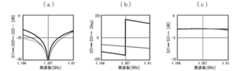
次に、本発明の円偏波アンテナ用給電回路の周波数特性について説明する。図5は、本発明の円偏波アンテナ用給電回路の周波数特性のグラフである。図5(a)がVSWR特性(S11,S22,S33)を、図5(b)が経路間の位相差(S21;S31)を、図5(c)が経路間の振幅比(S21;S31)をそれぞれ表している。図5のグラフは、具体的には図2に示されるように、2つの経路にそれぞれ位相遅れ回路及び位相進み回路からなる2つの位相シフト回路を接続し2つの経路間の位相差が90度となるような回路構成の場合のシミュレーショングラフである。また、比較例として従来技術の周波数特性のグラフを図6に示した。図6(a)がVSWR特性(S11,S22,S33)を、図6(b)が経路間の位相差(S21;S31)を、図6(c)が経路間の振幅比(S21;S31)をそれぞれ表している。図6のグラフは、具体的には従来技術の特許文献1に開示のもののように、90度の位相遅れ回路を用いた位相シフト回路が合成分配部と2つの給電点との間の一方の経路にのみ介在し、経路間の位相差が90度の位相差となるような回路構成の場合のシミュレーショングラフである。 Next, the frequency characteristics of the feeding circuit for the circularly polarized antenna of the present invention will be described. FIG. 5 is a graph of the frequency characteristics of the feeding circuit for a circularly polarized antenna of the present invention. FIG. 5 (a) shows VSWR characteristics (S11, S22, S33), FIG. 5 (b) shows the phase difference between paths (S21; S31), and FIG. 5 (c) shows the amplitude ratio between paths (S21; S31). ) Are represented respectively. In the graph of FIG. 5, specifically, as shown in FIG. 2, two phase shift circuits consisting of a phase delay circuit and a phase lead circuit are connected to each of the two paths, and the phase difference between the two paths is 90 degrees. It is a simulation graph in the case of a circuit configuration such that. Further, as a comparative example, a graph of the frequency characteristics of the prior art is shown in FIG. FIG. 6A shows VSWR characteristics (S11, S22, S33), FIG. 6B shows the phase difference between paths (S21; S31), and FIG. 6C shows the amplitude ratio between paths (S21; S31). ) Are represented respectively. In the graph of FIG. 6, specifically, as disclosed in
これらの図から分かる通り、従来技術では、1回路で−90度のシフトを行っているため、GNSSフルバンドにおいて、中心周波数(1387MHz)からずれるに従い、特に位相差90度を確保できず大きくずれることが分かる。したがって、1つの位相シフト回路ではGNSSフルバンド対応は困難であることが分かる。 As can be seen from these figures, in the prior art, a shift of -90 degrees is performed in one circuit, so that in the GNSS full band, as the deviation from the center frequency (1387 MHz), a phase difference of 90 degrees cannot be secured and the shift is large. You can see that. Therefore, it can be seen that it is difficult to support GNSS full band with one phase shift circuit.
一方、本発明の円偏波アンテナ用給電回路では、GNSSフルバンドにおいて、位相シフト回路の位相は中心周波数(1387MHz)からずれるに従い、個々に±45度からずれはするものの、両者は同様にずれていくため、結果として両者の位相差90度を常に確保できていることが分かる。このように、本発明の円偏波アンテナ用給電回路は、2つの給電点に接続される2つの経路間の位相差を広帯域わたって安定させることが可能であることが分かる。また、振幅比も広帯域にわたって小さいことも分かる。したがって、本発明の円偏波アンテナ用給電回路は、GNSSフルバンド対応が可能であることが分かる。 On the other hand, in the feeding circuit for the circularly polarized antenna of the present invention, in the GNSS full band, the phase of the phase shift circuit deviates from the center frequency (1387 MHz), and individually deviates from ± 45 degrees, but both deviate in the same manner. As a result, it can be seen that the phase difference between the two is always 90 degrees. As described above, it can be seen that the feeding circuit for the circularly polarized antenna of the present invention can stabilize the phase difference between the two paths connected to the two feeding points over a wide band. It can also be seen that the amplitude ratio is also small over a wide band. Therefore, it can be seen that the feeding circuit for the circularly polarized antenna of the present invention can support GNSS full band.
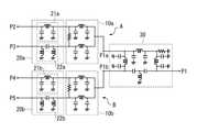
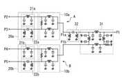
次に、本発明の円偏波アンテナ用給電回路を4点給電の円偏波アンテナに応用した場合について説明する。図7は、本発明の円偏波アンテナ用給電回路を4つの給電点に給電するように構成した例を説明するための具体的な回路図である。図中、図2と同一の符号を付した部分は同一物を表している。4点給電の給電点側は、上述の図示例と同じ給電回路を2つ用いており、これら2つの給電回路の入力端子(P1a,P1b)に180度の位相差を有する信号をそれぞれ入力するように構成したものである。 Next, a case where the feeding circuit for the circularly polarized antenna of the present invention is applied to the circularly polarized antenna of four-point feeding will be described. FIG. 7 is a specific circuit diagram for explaining an example in which the feeding circuit for a circularly polarized antenna of the present invention is configured to feed power to four feeding points. In the figure, the parts having the same reference numerals as those in FIG. 2 represent the same objects. On the feeding point side of the 4-point feeding, two feeding circuits same as those shown in the above illustration are used, and signals having a phase difference of 180 degrees are input to the input terminals (P1a, P1b) of these two feeding circuits, respectively. It is configured as follows.
図7に示される例では、上述の図示例と同じ構成の給電回路を3つ用いている。即ち、4点給電円偏波アンテナ用給電回路は、上述の図2に示される円偏波アンテナ用給電回路と同様にそれぞれ構成される第1給電回路Aと、第2給電回路Bと、180度合成分配部として構成される第3給電回路Cとからなる。 In the example shown in FIG. 7, three power feeding circuits having the same configuration as the above illustrated example are used. That is, the four-point feeding circularly polarized antenna feeding circuit includes the first feeding circuit A, the second feeding circuit B, and 180, which are configured in the same manner as the circularly polarized antenna feeding circuit shown in FIG. It is composed of a third power feeding circuit C configured as a combined distribution unit.
第1給電回路Aは、第1合成分配部10aと、第1位相シフト部20aとからなる。第1合成分配部10aは、第1入力端子P1aからの信号を同相且つ同振幅で2つの経路に分配するものである。第1位相シフト部20aは、集中定数回路で構成される2つの第1位相シフト回路21a,22aを有する。2つの第1位相シフト回路21a,22aは、第1合成分配部10aにより分配される2つの経路と4つの給電点P2,P3,P4,P5のうち2つの給電点P2,P3との間にそれぞれ接続されている。第1位相シフト回路21a,22aは、給電点P2,P3へ位相差が90度となる信号をそれぞれ出力する。例えば第1位相シフト回路21aが−45度位相をシフトし、第1位相シフト回路22aが+45度位相をシフトするものであれば良い。 The first feeding circuit A includes a first
また、第2給電回路Bは、第2合成分配部10bと、第2位相シフト部20bとからなる。第2合成分配部10bは、第2入力端子P1bからの信号を同相且つ同振幅で2つの経路に分配するものである。第2位相シフト部20bは、集中定数回路で構成される2つの第2位相シフト回路21b,22bを有する。2つの第2位相シフト回路21b,22bは、第2合成分配部10bにより分配される2つの経路と4つの給電点P2,P3,P4,P5のうち残りの2つの給電点P4,P5との間にそれぞれ接続されている。第2位相シフト回路21b,22bは、給電点P4,P5へ位相差が90度となる信号をそれぞれ出力する。例えば第2位相シフト回路21bが−45度位相をシフトし、第2位相シフト回路22bが+45度位相をシフトするものであれば良い。 Further, the second feeding circuit B includes a second combined
そして、180度合成分配部として構成される第3給電回路Cは、基本的な構成は第1給電回路A及び第2給電回路Bと同様であるが、入力信号を2つの経路に180度の位相差を有するように分配するように構成されている。第3給電回路Cは、第3合成分配部10cと、第3位相シフト部20cとからなる。第3合成分配部10cは、ポートP1からの入力信号を同相且つ同振幅で2つの経路に分配するものである。第3位相シフト部20cは、集中定数回路で構成される2つの第3位相シフト回路21c,22cを有する。2つの第3位相シフト回路21c,22cは、第1入力端子P1aと第2入力端子P1bへ位相差が180度となる信号をそれぞれ出力する。例えば第3位相シフト回路21cが−90度位相をシフトし、第3位相シフト回路22cが+90度位相をシフトするものであれば良い。 The third power supply circuit C configured as the 180-degree composite distribution unit has the same basic configuration as the first power supply circuit A and the second power supply circuit B, but the input signal is 180 degrees in two paths. It is configured to distribute so as to have a phase difference. The third power feeding circuit C includes a third
このように構成されることで、ポートP1からの入力信号が第3合成分配部10cで同相且つ同振幅で2つの経路に分配され、それぞれ第3位相シフト回路21c及び第3位相シフト回路22cに入力される。そして、2つの経路間の位相差が180度の信号がそれぞれ第1給電回路Aの第1入力端子P1a及び第2給電回路Bの第2入力端子P1bに入力される。第1給電回路Aでは、入力された信号を第1合成分配部10aで同相且つ同振幅で分配し、第1位相シフト回路21a,22aをそれぞれ介して位相差が90度となる信号を給電点P2,P3に入力する。同様に、第2給電回路Bでは、入力された信号を第2合成分配部10bで同相且つ同振幅で分配し、第2位相シフト回路21b,22bをそれぞれ介して位相差が90度となる信号を給電点P4,P5に入力する。即ち、給電点P2には−135度の信号が、給電点P3には−45度の信号が、給電点P4には+45度の信号が、給電点P5には+135度の信号がそれぞれ入力されることになる。 With this configuration, the input signal from the port P1 is distributed to the two paths with the same phase and the same amplitude by the third
さらに、本発明の円偏波アンテナ用給電回路を4点給電の円偏波アンテナに応用した他の例を説明する。図8は、本発明の円偏波アンテナ用給電回路を4つの給電点に給電するように構成した他の例を説明するための具体的な回路図である。図中、図7と同一の符号を付した部分は同一物を表している。図示の通り、この例では、上述の図示例と同じ構成の給電回路を2つ用いている。即ち、4点給電円偏波アンテナ用給電回路は、上述の図2に示される円偏波アンテナ用給電回路と同様にそれぞれ構成される第1給電回路Aと、第2給電回路Bとを用いている。そして、図7に示される例と異なり、第1入力端子P1aと第2入力端子P1bへ位相差が180度となる信号をそれぞれ出力する180度合成分配部として、180度ラットレース回路30を用いている。180度ラットレース回路30は、ポートP1からの入力信号を2つの経路に180度の位相差を有するように分配するものである。図示の通り、180度ラットレース回路30により分配される2つの経路は、第1入力端子P1aと第2入力端子P1bにそれぞれ接続される。したがって、第1入力端子P1aと第2入力端子P1bへは、位相差が180度となる信号が入力される。なお、第1給電回路Aと第2給電回路Bの構成は図7と同様のため、説明は省略する。 Further, another example in which the feeding circuit for the circularly polarized antenna of the present invention is applied to the circularly polarized antenna of four-point feeding will be described. FIG. 8 is a specific circuit diagram for explaining another example in which the feeding circuit for a circularly polarized antenna of the present invention is configured to feed power to four feeding points. In the figure, the parts with the same reference numerals as those in FIG. 7 represent the same objects. As shown in the figure, in this example, two power supply circuits having the same configuration as the above-mentioned illustrated example are used. That is, the four-point feeding circularly polarized antenna feeding circuit uses the first feeding circuit A and the second feeding circuit B, which are respectively configured in the same manner as the circularly polarized antenna feeding circuit shown in FIG. ing. Then, unlike the example shown in FIG. 7, a 180-degree
図示例では180度ラットレース回路30が3つのCLCのπ型フィルタ回路と1つのCLCのT型フィルタ回路を組み合わせたものを示したが、本発明はこれに限定されず、3つのLCLのπ型フィルタ回路と1つのCLCのπ型フィルタ回路を組み合わせた180度ラットレース回路であっても良い。 In the illustrated example, the 180-degree
さらにまた、180度合成分配部として、90度ハイブリッド回路と90度位相シフト回路を組み合わせたものを用いても良い。図9は、本発明の円偏波アンテナ用給電回路を4つの給電点に給電するように構成したさらに他の例を説明するための具体的な回路図である。図中、図8と同一の符号を付した部分は同一物を表している。図示の通り、この例では、180度合成分配部として、90度ハイブリッド回路31と90度位相シフト回路32を用いて第1入力端子P1aと第2入力端子P1bへ位相差が180度となる信号をそれぞれ出力するようにしている。図示の通り、90度ハイブリッド回路31により分配される2つの経路は、ポートP1からの入力信号を2つの経路に90度の位相差を有するように分配するものである。そして、90度ハイブリッド回路31により分配される2つの経路は、その一方の経路に90度位相シフト回路32が接続されている。そして、90度位相シフト回路32からの経路が第1入力端子P1aに接続されている。また、90度ハイブリッド回路31により分配される2つの経路の他方の経路は直接第2入力端子P1bに接続されている。したがって、第1入力端子P1aと第2入力端子P1bへは、位相差が180度となる信号が入力される。なお、第1給電回路Aと第2給電回路Bの構成は図7と同様のため、説明は省略する。 Furthermore, as the 180-degree composite distribution unit, a combination of a 90-degree hybrid circuit and a 90-degree phase shift circuit may be used. FIG. 9 is a specific circuit diagram for explaining still another example in which the feeding circuit for a circularly polarized antenna of the present invention is configured to feed power to four feeding points. In the figure, the parts having the same reference numerals as those in FIG. 8 represent the same objects. As shown in the figure, in this example, a 90-degree hybrid circuit 31 and a 90-degree
なお、図7乃至図9に示される本発明の4点給電円偏波アンテナ用給電回路も、上述の図示例と同様に、集中定数回路や分布定数回路で構成されれば良い。 The four-point feeding circularly polarized wave antenna feeding circuit of the present invention shown in FIGS. 7 to 9 may also be composed of a lumped constant circuit or a distributed constant circuit, as in the above illustrated example.
このように、本発明の円偏波アンテナ用給電回路は、2点給電だけでなく4点給電の円偏波アンテナにも種々応用可能である。 As described above, the feeding circuit for the circularly polarized antenna of the present invention can be variously applied not only to the two-point feeding but also to the four-point feeding circularly polarized antenna.
なお、本発明の円偏波アンテナ用給電回路は、上述の図示例にのみ限定されるものではなく、本発明の要旨を逸脱しない範囲内において種々変更を加え得ることは勿論である。 The feeding circuit for a circularly polarized antenna of the present invention is not limited to the above illustrated example, and it goes without saying that various modifications can be made without departing from the gist of the present invention.
1 円偏波アンテナ
10 合成分配部
10a 第1合成分配部
10b 第2合成分配部
10c 第3合成分配部
20 位相シフト部
20a 第1位相シフト部
20b 第2位相シフト部
20c 第3位相シフト部
21 位相シフト回路
21a 第1位相シフト回路
21b 第2位相シフト回路
21c 第3位相シフト回路
22 位相シフト回路
22a 第1位相シフト回路
22b 第2位相シフト回路
22c 第3位相シフト回路
30 180度ラットレース回路
31 90度ハイブリッド回路
32 90度位相シフト回路
A 第1給電回路
B 第2給電回路
C 第3給電回路
P1 ポート
P2,P3,P4,P5 給電点1 Circularly polarized
Claims (11)
Translated fromJapanese入力信号を同相且つ同振幅で2つの経路に分配する合成分配部と、
前記合成分配部により分配される2つの経路と円偏波アンテナの2つの給電点との間にそれぞれ接続される2つの位相シフト回路を有する位相シフト部であって、円偏波アンテナの2つの給電点へ位相差が90度となる信号をそれぞれ出力する位相シフト部と、
を具備することを特徴とする円偏波アンテナ用給電回路。A feeding circuit for feeding power to a circularly polarized antenna, and the feeding circuit for the circularly polarized antenna is
A composite distributor that distributes the input signal to two paths with the same phase and amplitude.
It is a phase shift unit having two phase shift circuits connected between the two paths distributed by the composite distribution unit and the two feeding points of the circularly polarized antenna, and two of the circularly polarized antennas. A phase shift unit that outputs signals with a phase difference of 90 degrees to the feeding point, and
A feeding circuit for a circularly polarized antenna.
第1入力端子からの信号を同相且つ同振幅で2つの経路に分配する第1合成分配部と、該第1合成分配部により分配される2つの経路と円偏波アンテナの4つの給電点のうち2つの給電点との間にそれぞれ接続される2つの第1位相シフト回路を有する第1位相シフト部であって、円偏波アンテナの4つの給電点のうち2つの給電点へ位相差が90度となる信号をそれぞれ出力する第1位相シフト部と、からなる第1給電回路と、
第2入力端子からの信号を同相且つ同振幅で2つの経路に分配する第2合成分配部と、該第2合成分配部により分配される2つの経路と円偏波アンテナの4つの給電点のうち残りの2つの給電点との間にそれぞれ接続される2つの第2位相シフト回路を有する第2位相シフト部であって、円偏波アンテナの4つの給電点のうち残りの2つの給電点へ位相差が90度となる信号をそれぞれ出力する第2位相シフト部と、からなる第2給電回路と、
入力信号を2つの経路に180度の位相差を有するように分配する180度合成分配部であって、180度合成分配部により分配される2つの経路が第1入力端子と第2入力端子にそれぞれ接続され、第1入力端子と第2入力端子へ位相差が180度となる信号をそれぞれ出力する180度合成分配部と、
を具備することを特徴とする4点給電円偏波アンテナ用給電回路。A power feeding circuit for supplying power to a 4-point feeding circularly polarized antenna, and the feeding circuit for the 4-point feeding circularly polarized antenna is
The first synthetic distribution unit that distributes the signal from the first input terminal to two paths with the same phase and the same amplitude, the two paths distributed by the first synthetic distribution unit, and the four feeding points of the circularly polarized antenna. It is a first phase shift unit having two first phase shift circuits connected to each of the two feeding points, and the phase difference is applied to two feeding points out of the four feeding points of the circularly polarized antenna. A first power supply circuit consisting of a first phase shift unit that outputs signals at 90 degrees, and
The second synthetic distribution unit that distributes the signal from the second input terminal to two paths with the same phase and the same amplitude, the two paths distributed by the second synthetic distribution unit, and the four feeding points of the circularly polarized antenna. A second phase shift unit having two second phase shift circuits connected to each of the remaining two feeding points, and the remaining two feeding points out of the four feeding points of the circularly polarized antenna. A second power supply circuit consisting of a second phase shift unit that outputs signals having a phase difference of 90 degrees to each other.
A 180-degree composite distributor that distributes an input signal to two paths so as to have a 180-degree phase difference, and the two paths distributed by the 180-degree composite distributor are connected to the first input terminal and the second input terminal. A 180-degree composite distribution unit that is connected to each other and outputs signals with a phase difference of 180 degrees to the first input terminal and the second input terminal, respectively.
A feeding circuit for a 4-point feeding circularly polarized wave antenna, which comprises.
入力信号を同相且つ同振幅で2つの経路に分配する第3合成分配部と、
前記第3合成分配部により分配される2つの経路と第1入力端子及び第2入力端子との間にそれぞれ接続される2つの第3位相シフト回路を有する第3位相シフト部と、
からなることを特徴とする4点給電円偏波アンテナ用給電回路。In the power feeding circuit for a four-point feeding circularly polarized wave antenna according to claim 8, the 180-degree composite distribution unit is used.
A third composite distributor that distributes the input signal to two paths with the same phase and amplitude.
A third phase shift unit having two third phase shift circuits connected between the two paths distributed by the third composite distribution unit and the first input terminal and the second input terminal, respectively.
A feeding circuit for a 4-point feeding circularly polarized antenna, which is characterized by being composed of.
入力信号を2つの経路に90度の位相差を有するように分配する90度ハイブリッド回路と、
前記90度ハイブリッド回路により分配される2つの経路の一方の経路に接続される90度位相シフト回路と、からなり、
前記90度位相シフト回路からの経路が第1入力端子に接続され、90度ハイブリッド回路により分配される2つの経路の他方の経路が第2入力端子に接続される、
ことを特徴とする4点給電円偏波アンテナ用給電回路。In the power feeding circuit for a four-point feeding circularly polarized wave antenna according to claim 8, the 180-degree composite distribution unit is used.
A 90-degree hybrid circuit that distributes the input signal to the two paths so as to have a 90-degree phase difference.
It consists of a 90 degree phase shift circuit connected to one of the two paths distributed by the 90 degree hybrid circuit.
The path from the 90 degree phase shift circuit is connected to the first input terminal, and the other path of the two paths distributed by the 90 degree hybrid circuit is connected to the second input terminal.
A power supply circuit for a 4-point power supply circularly polarized antenna.
Priority Applications (5)
| Application Number | Priority Date | Filing Date | Title |
|---|---|---|---|
| JP2020000527AJP7101201B2 (en) | 2020-01-06 | 2020-01-06 | Power supply circuit for circularly polarized antenna |
| DE112020006456.5TDE112020006456T5 (en) | 2020-01-06 | 2020-11-09 | POWER SUPPLY CIRCUIT FOR A CIRCULAR POLARIZED ANTENNA |
| CN202080091950.3ACN115023857A (en) | 2020-01-06 | 2020-11-09 | Feed circuit for circularly polarized antenna |
| PCT/JP2020/041784WO2021140738A1 (en) | 2020-01-06 | 2020-11-09 | Power feeder circuit for circularly polarized antenna |
| US17/790,485US12218394B2 (en) | 2020-01-06 | 2020-11-09 | Power feed circuit comprising a synthesizing-distributing unit and a phase shifting unit configured for feeding a two point or a four point circularly polarized antenna |
Applications Claiming Priority (1)
| Application Number | Priority Date | Filing Date | Title |
|---|---|---|---|
| JP2020000527AJP7101201B2 (en) | 2020-01-06 | 2020-01-06 | Power supply circuit for circularly polarized antenna |
Publications (2)
| Publication Number | Publication Date |
|---|---|
| JP2021111813Atrue JP2021111813A (en) | 2021-08-02 |
| JP7101201B2 JP7101201B2 (en) | 2022-07-14 |
Family
ID=76787850
Family Applications (1)
| Application Number | Title | Priority Date | Filing Date |
|---|---|---|---|
| JP2020000527AActiveJP7101201B2 (en) | 2020-01-06 | 2020-01-06 | Power supply circuit for circularly polarized antenna |
Country Status (5)
| Country | Link |
|---|---|
| US (1) | US12218394B2 (en) |
| JP (1) | JP7101201B2 (en) |
| CN (1) | CN115023857A (en) |
| DE (1) | DE112020006456T5 (en) |
| WO (1) | WO2021140738A1 (en) |
Cited By (2)
| Publication number | Priority date | Publication date | Assignee | Title |
|---|---|---|---|---|
| WO2023127595A1 (en)* | 2021-12-27 | 2023-07-06 | 株式会社ヨコオ | Antenna and circuit board |
| JP2023150996A (en)* | 2022-03-31 | 2023-10-16 | 原田工業株式会社 | Power supply circuit for circularly polarized antenna and circularly polarized antenna device |
Citations (3)
| Publication number | Priority date | Publication date | Assignee | Title |
|---|---|---|---|---|
| JPH06169219A (en)* | 1991-05-27 | 1994-06-14 | Yuseisho Tsushin Sogo Kenkyusho | Multi-point feeding circularly polarized wave antenna |
| JP2004056204A (en)* | 2002-07-16 | 2004-02-19 | Alps Electric Co Ltd | Patch antenna |
| WO2017026107A1 (en)* | 2015-08-07 | 2017-02-16 | 日本電気株式会社 | Demultiplexer/multiplexer, antenna device, and fading elimination method |
Family Cites Families (15)
| Publication number | Priority date | Publication date | Assignee | Title |
|---|---|---|---|---|
| FR2623020B1 (en)* | 1987-11-05 | 1990-02-16 | Alcatel Espace | DEVICE FOR EXCITTING A CIRCULAR POLARIZATION WAVEGUIDE BY A PLANE ANTENNA |
| GB8816276D0 (en)* | 1988-07-08 | 1988-08-10 | Marconi Co Ltd | Waveguide coupler |
| JPH04368002A (en)* | 1991-06-14 | 1992-12-21 | Sony Corp | Polarized wave converter |
| JPH11127004A (en) | 1997-10-22 | 1999-05-11 | Sharp Corp | High frequency circuit |
| JP2008017159A (en) | 2006-07-06 | 2008-01-24 | Toyama Univ | Transmission line type lumped constant Wilkinson divider with two types of phase shifters |
| JP2010021630A (en)* | 2008-07-08 | 2010-01-28 | Nippon Antenna Co Ltd | Wide-band balun |
| CN201435450Y (en)* | 2009-06-30 | 2010-03-31 | 华南理工大学 | Polarized Reconfigurable RFID Circularly Polarized Reader Antenna |
| CN101859927B (en)* | 2010-04-14 | 2012-12-05 | 电子科技大学 | LTCC lamination double-fed circularly polarized micro-strip paster antenna |
| CN102790292B (en)* | 2012-08-03 | 2015-07-29 | 北京敏视达雷达有限公司 | A kind of circular polarization satellite navigation aerial, preparation method and antenna circuit |
| JP6235813B2 (en) | 2013-07-09 | 2017-11-22 | 株式会社ヨコオ | Microstrip antenna |
| CN103367933A (en)* | 2013-07-16 | 2013-10-23 | 深圳市华信天线技术有限公司 | Antenna assembly |
| US9013246B2 (en) | 2013-08-01 | 2015-04-21 | Freescale Semiconductor, Inc. | Coupler with distributed feeding and compensation |
| CN103606743A (en)* | 2013-10-25 | 2014-02-26 | 深圳市摩天射频技术有限公司 | Circularly-polarized wideband antenna |
| KR101688899B1 (en)* | 2015-09-03 | 2016-12-23 | 경북대학교 산학협력단 | Broad band balun and dipole antenna using the same elements |
| CN110350310B (en)* | 2018-04-08 | 2024-04-23 | 京东方科技集团股份有限公司 | Antenna structure and modulation method thereof |
- 2020
- 2020-01-06JPJP2020000527Apatent/JP7101201B2/enactiveActive
- 2020-11-09CNCN202080091950.3Apatent/CN115023857A/enactivePending
- 2020-11-09WOPCT/JP2020/041784patent/WO2021140738A1/ennot_activeCeased
- 2020-11-09USUS17/790,485patent/US12218394B2/enactiveActive
- 2020-11-09DEDE112020006456.5Tpatent/DE112020006456T5/enactivePending
Patent Citations (3)
| Publication number | Priority date | Publication date | Assignee | Title |
|---|---|---|---|---|
| JPH06169219A (en)* | 1991-05-27 | 1994-06-14 | Yuseisho Tsushin Sogo Kenkyusho | Multi-point feeding circularly polarized wave antenna |
| JP2004056204A (en)* | 2002-07-16 | 2004-02-19 | Alps Electric Co Ltd | Patch antenna |
| WO2017026107A1 (en)* | 2015-08-07 | 2017-02-16 | 日本電気株式会社 | Demultiplexer/multiplexer, antenna device, and fading elimination method |
Non-Patent Citations (1)
| Title |
|---|
| HARVINDER SINGH NAGI: "Miniature lumped element 180° Wilkinson Divider", IEEE MTT-S INTERNATIONAL MICROWAVE SYMPOSIUM DIGEST, 2003, vol. 1, JPN6021002431, 2003, US, pages 55 - 58, XP055840147, ISSN: 0004676409* |
Cited By (2)
| Publication number | Priority date | Publication date | Assignee | Title |
|---|---|---|---|---|
| WO2023127595A1 (en)* | 2021-12-27 | 2023-07-06 | 株式会社ヨコオ | Antenna and circuit board |
| JP2023150996A (en)* | 2022-03-31 | 2023-10-16 | 原田工業株式会社 | Power supply circuit for circularly polarized antenna and circularly polarized antenna device |
Also Published As
| Publication number | Publication date |
|---|---|
| CN115023857A (en) | 2022-09-06 |
| DE112020006456T5 (en) | 2022-10-27 |
| JP7101201B2 (en) | 2022-07-14 |
| WO2021140738A1 (en) | 2021-07-15 |
| US20230044376A1 (en) | 2023-02-09 |
| US12218394B2 (en) | 2025-02-04 |
Similar Documents
| Publication | Publication Date | Title |
|---|---|---|
| CN111344895A (en) | Power coupler with antenna element power sink and related apparatus | |
| US7633358B2 (en) | Phase shifter circuit with proper broadband performance | |
| JP7101201B2 (en) | Power supply circuit for circularly polarized antenna | |
| CN103580637A (en) | Balun transformer | |
| KR20130123305A (en) | Doherty amplifier | |
| WO2015052838A1 (en) | Decoupling circuit | |
| JP2008236105A (en) | Power dividing/combining system | |
| US11689176B2 (en) | Power divider comprising a plurality of (90/N)-degree phase shift circuit blocks formed by inductor and capacitor circuitry | |
| US11217871B2 (en) | Distributor and synthesizer | |
| JPH0537212A (en) | Power distribution combiner | |
| JP5065667B2 (en) | High frequency power amplifier | |
| US20230106157A1 (en) | Phase shifter and phased array antenna device | |
| US7982556B2 (en) | Splitter with a printed element | |
| KR102019060B1 (en) | Branch circuit | |
| JP2004320408A (en) | Distributor and high-frequency signal transmitting / receiving device using the same | |
| JP5652185B2 (en) | Group delay time adjustment circuit and power distribution / synthesis circuit | |
| JP4771930B2 (en) | High frequency quadrature detector | |
| US20240219513A1 (en) | Device for generating iq signals and method for producing a device for generating iq signals | |
| US20240305007A1 (en) | Transmission line arrangement for a passive component | |
| JP2023150996A (en) | Power supply circuit for circularly polarized antenna and circularly polarized antenna device | |
| JP2692916B2 (en) | High frequency power distributor | |
| WO2025152126A1 (en) | Stacked branch-line coupler | |
| CN120263125A (en) | Balanced power amplifier synthesis circuit and RF power supply | |
| WO2022172836A1 (en) | Divider and communication device | |
| JP4771929B2 (en) | High frequency quadrature detector |
Legal Events
| Date | Code | Title | Description |
|---|---|---|---|
| A621 | Written request for application examination | Free format text:JAPANESE INTERMEDIATE CODE: A621 Effective date:20211119 | |
| A871 | Explanation of circumstances concerning accelerated examination | Free format text:JAPANESE INTERMEDIATE CODE: A871 Effective date:20211119 | |
| A131 | Notification of reasons for refusal | Free format text:JAPANESE INTERMEDIATE CODE: A131 Effective date:20220105 | |
| A131 | Notification of reasons for refusal | Free format text:JAPANESE INTERMEDIATE CODE: A131 Effective date:20220601 | |
| A521 | Request for written amendment filed | Free format text:JAPANESE INTERMEDIATE CODE: A523 Effective date:20220608 | |
| TRDD | Decision of grant or rejection written | ||
| A01 | Written decision to grant a patent or to grant a registration (utility model) | Free format text:JAPANESE INTERMEDIATE CODE: A01 Effective date:20220622 | |
| A61 | First payment of annual fees (during grant procedure) | Free format text:JAPANESE INTERMEDIATE CODE: A61 Effective date:20220704 | |
| R150 | Certificate of patent or registration of utility model | Ref document number:7101201 Country of ref document:JP Free format text:JAPANESE INTERMEDIATE CODE: R150 | |
| R250 | Receipt of annual fees | Free format text:JAPANESE INTERMEDIATE CODE: R250 |