JP2021103322A - Display - Google Patents
DisplayDownload PDFInfo
- Publication number
- JP2021103322A JP2021103322AJP2021047152AJP2021047152AJP2021103322AJP 2021103322 AJP2021103322 AJP 2021103322AJP 2021047152 AJP2021047152 AJP 2021047152AJP 2021047152 AJP2021047152 AJP 2021047152AJP 2021103322 AJP2021103322 AJP 2021103322A
- Authority
- JP
- Japan
- Prior art keywords
- transistor
- electrode
- switch
- light emitting
- pixel
- Prior art date
- Legal status (The legal status is an assumption and is not a legal conclusion. Google has not performed a legal analysis and makes no representation as to the accuracy of the status listed.)
- Withdrawn
Links
Images


Classifications
- H—ELECTRICITY
- H05—ELECTRIC TECHNIQUES NOT OTHERWISE PROVIDED FOR
- H05B—ELECTRIC HEATING; ELECTRIC LIGHT SOURCES NOT OTHERWISE PROVIDED FOR; CIRCUIT ARRANGEMENTS FOR ELECTRIC LIGHT SOURCES, IN GENERAL
- H05B33/00—Electroluminescent light sources
- H05B33/10—Apparatus or processes specially adapted to the manufacture of electroluminescent light sources
- G—PHYSICS
- G09—EDUCATION; CRYPTOGRAPHY; DISPLAY; ADVERTISING; SEALS
- G09G—ARRANGEMENTS OR CIRCUITS FOR CONTROL OF INDICATING DEVICES USING STATIC MEANS TO PRESENT VARIABLE INFORMATION
- G09G3/00—Control arrangements or circuits, of interest only in connection with visual indicators other than cathode-ray tubes
- G09G3/20—Control arrangements or circuits, of interest only in connection with visual indicators other than cathode-ray tubes for presentation of an assembly of a number of characters, e.g. a page, by composing the assembly by combination of individual elements arranged in a matrix no fixed position being assigned to or needed to be assigned to the individual characters or partial characters
- G09G3/22—Control arrangements or circuits, of interest only in connection with visual indicators other than cathode-ray tubes for presentation of an assembly of a number of characters, e.g. a page, by composing the assembly by combination of individual elements arranged in a matrix no fixed position being assigned to or needed to be assigned to the individual characters or partial characters using controlled light sources
- G09G3/30—Control arrangements or circuits, of interest only in connection with visual indicators other than cathode-ray tubes for presentation of an assembly of a number of characters, e.g. a page, by composing the assembly by combination of individual elements arranged in a matrix no fixed position being assigned to or needed to be assigned to the individual characters or partial characters using controlled light sources using electroluminescent panels
- G09G3/32—Control arrangements or circuits, of interest only in connection with visual indicators other than cathode-ray tubes for presentation of an assembly of a number of characters, e.g. a page, by composing the assembly by combination of individual elements arranged in a matrix no fixed position being assigned to or needed to be assigned to the individual characters or partial characters using controlled light sources using electroluminescent panels semiconductive, e.g. using light-emitting diodes [LED]
- G09G3/3208—Control arrangements or circuits, of interest only in connection with visual indicators other than cathode-ray tubes for presentation of an assembly of a number of characters, e.g. a page, by composing the assembly by combination of individual elements arranged in a matrix no fixed position being assigned to or needed to be assigned to the individual characters or partial characters using controlled light sources using electroluminescent panels semiconductive, e.g. using light-emitting diodes [LED] organic, e.g. using organic light-emitting diodes [OLED]
- G09G3/3225—Control arrangements or circuits, of interest only in connection with visual indicators other than cathode-ray tubes for presentation of an assembly of a number of characters, e.g. a page, by composing the assembly by combination of individual elements arranged in a matrix no fixed position being assigned to or needed to be assigned to the individual characters or partial characters using controlled light sources using electroluminescent panels semiconductive, e.g. using light-emitting diodes [LED] organic, e.g. using organic light-emitting diodes [OLED] using an active matrix
- G09G3/3233—Control arrangements or circuits, of interest only in connection with visual indicators other than cathode-ray tubes for presentation of an assembly of a number of characters, e.g. a page, by composing the assembly by combination of individual elements arranged in a matrix no fixed position being assigned to or needed to be assigned to the individual characters or partial characters using controlled light sources using electroluminescent panels semiconductive, e.g. using light-emitting diodes [LED] organic, e.g. using organic light-emitting diodes [OLED] using an active matrix with pixel circuitry controlling the current through the light-emitting element
- G—PHYSICS
- G09—EDUCATION; CRYPTOGRAPHY; DISPLAY; ADVERTISING; SEALS
- G09G—ARRANGEMENTS OR CIRCUITS FOR CONTROL OF INDICATING DEVICES USING STATIC MEANS TO PRESENT VARIABLE INFORMATION
- G09G2300/00—Aspects of the constitution of display devices
- G09G2300/04—Structural and physical details of display devices
- G09G2300/0421—Structural details of the set of electrodes
- G09G2300/0426—Layout of electrodes and connections
- G—PHYSICS
- G09—EDUCATION; CRYPTOGRAPHY; DISPLAY; ADVERTISING; SEALS
- G09G—ARRANGEMENTS OR CIRCUITS FOR CONTROL OF INDICATING DEVICES USING STATIC MEANS TO PRESENT VARIABLE INFORMATION
- G09G2300/00—Aspects of the constitution of display devices
- G09G2300/04—Structural and physical details of display devices
- G09G2300/0439—Pixel structures
- G09G2300/0465—Improved aperture ratio, e.g. by size reduction of the pixel circuit, e.g. for improving the pixel density or the maximum displayable luminance or brightness
- G—PHYSICS
- G09—EDUCATION; CRYPTOGRAPHY; DISPLAY; ADVERTISING; SEALS
- G09G—ARRANGEMENTS OR CIRCUITS FOR CONTROL OF INDICATING DEVICES USING STATIC MEANS TO PRESENT VARIABLE INFORMATION
- G09G2300/00—Aspects of the constitution of display devices
- G09G2300/08—Active matrix structure, i.e. with use of active elements, inclusive of non-linear two terminal elements, in the pixels together with light emitting or modulating elements
- G09G2300/0809—Several active elements per pixel in active matrix panels
- G09G2300/0819—Several active elements per pixel in active matrix panels used for counteracting undesired variations, e.g. feedback or autozeroing
- G—PHYSICS
- G09—EDUCATION; CRYPTOGRAPHY; DISPLAY; ADVERTISING; SEALS
- G09G—ARRANGEMENTS OR CIRCUITS FOR CONTROL OF INDICATING DEVICES USING STATIC MEANS TO PRESENT VARIABLE INFORMATION
- G09G2300/00—Aspects of the constitution of display devices
- G09G2300/08—Active matrix structure, i.e. with use of active elements, inclusive of non-linear two terminal elements, in the pixels together with light emitting or modulating elements
- G09G2300/0809—Several active elements per pixel in active matrix panels
- G09G2300/0842—Several active elements per pixel in active matrix panels forming a memory circuit, e.g. a dynamic memory with one capacitor
- G09G2300/0852—Several active elements per pixel in active matrix panels forming a memory circuit, e.g. a dynamic memory with one capacitor being a dynamic memory with more than one capacitor
- G—PHYSICS
- G09—EDUCATION; CRYPTOGRAPHY; DISPLAY; ADVERTISING; SEALS
- G09G—ARRANGEMENTS OR CIRCUITS FOR CONTROL OF INDICATING DEVICES USING STATIC MEANS TO PRESENT VARIABLE INFORMATION
- G09G2300/00—Aspects of the constitution of display devices
- G09G2300/08—Active matrix structure, i.e. with use of active elements, inclusive of non-linear two terminal elements, in the pixels together with light emitting or modulating elements
- G09G2300/0809—Several active elements per pixel in active matrix panels
- G09G2300/0842—Several active elements per pixel in active matrix panels forming a memory circuit, e.g. a dynamic memory with one capacitor
- G09G2300/0861—Several active elements per pixel in active matrix panels forming a memory circuit, e.g. a dynamic memory with one capacitor with additional control of the display period without amending the charge stored in a pixel memory, e.g. by means of additional select electrodes
- G—PHYSICS
- G09—EDUCATION; CRYPTOGRAPHY; DISPLAY; ADVERTISING; SEALS
- G09G—ARRANGEMENTS OR CIRCUITS FOR CONTROL OF INDICATING DEVICES USING STATIC MEANS TO PRESENT VARIABLE INFORMATION
- G09G2310/00—Command of the display device
- G09G2310/02—Addressing, scanning or driving the display screen or processing steps related thereto
- G09G2310/0243—Details of the generation of driving signals
- G09G2310/0251—Precharge or discharge of pixel before applying new pixel voltage
- G—PHYSICS
- G09—EDUCATION; CRYPTOGRAPHY; DISPLAY; ADVERTISING; SEALS
- G09G—ARRANGEMENTS OR CIRCUITS FOR CONTROL OF INDICATING DEVICES USING STATIC MEANS TO PRESENT VARIABLE INFORMATION
- G09G2310/00—Command of the display device
- G09G2310/02—Addressing, scanning or driving the display screen or processing steps related thereto
- G09G2310/0262—The addressing of the pixel, in a display other than an active matrix LCD, involving the control of two or more scan electrodes or two or more data electrodes, e.g. pixel voltage dependent on signals of two data electrodes
- G—PHYSICS
- G09—EDUCATION; CRYPTOGRAPHY; DISPLAY; ADVERTISING; SEALS
- G09G—ARRANGEMENTS OR CIRCUITS FOR CONTROL OF INDICATING DEVICES USING STATIC MEANS TO PRESENT VARIABLE INFORMATION
- G09G2320/00—Control of display operating conditions
- G09G2320/02—Improving the quality of display appearance
- G09G2320/0233—Improving the luminance or brightness uniformity across the screen
- G—PHYSICS
- G09—EDUCATION; CRYPTOGRAPHY; DISPLAY; ADVERTISING; SEALS
- G09G—ARRANGEMENTS OR CIRCUITS FOR CONTROL OF INDICATING DEVICES USING STATIC MEANS TO PRESENT VARIABLE INFORMATION
- G09G2320/00—Control of display operating conditions
- G09G2320/04—Maintaining the quality of display appearance
- G09G2320/043—Preventing or counteracting the effects of ageing
- G09G2320/045—Compensation of drifts in the characteristics of light emitting or modulating elements
- G—PHYSICS
- G09—EDUCATION; CRYPTOGRAPHY; DISPLAY; ADVERTISING; SEALS
- G09G—ARRANGEMENTS OR CIRCUITS FOR CONTROL OF INDICATING DEVICES USING STATIC MEANS TO PRESENT VARIABLE INFORMATION
- G09G2330/00—Aspects of power supply; Aspects of display protection and defect management
- G09G2330/02—Details of power systems and of start or stop of display operation
- G09G2330/021—Power management, e.g. power saving
- G—PHYSICS
- G09—EDUCATION; CRYPTOGRAPHY; DISPLAY; ADVERTISING; SEALS
- G09G—ARRANGEMENTS OR CIRCUITS FOR CONTROL OF INDICATING DEVICES USING STATIC MEANS TO PRESENT VARIABLE INFORMATION
- G09G3/00—Control arrangements or circuits, of interest only in connection with visual indicators other than cathode-ray tubes
- G09G3/20—Control arrangements or circuits, of interest only in connection with visual indicators other than cathode-ray tubes for presentation of an assembly of a number of characters, e.g. a page, by composing the assembly by combination of individual elements arranged in a matrix no fixed position being assigned to or needed to be assigned to the individual characters or partial characters
- G09G3/2007—Display of intermediate tones
- G09G3/2018—Display of intermediate tones by time modulation using two or more time intervals
- G09G3/2022—Display of intermediate tones by time modulation using two or more time intervals using sub-frames
- H—ELECTRICITY
- H10—SEMICONDUCTOR DEVICES; ELECTRIC SOLID-STATE DEVICES NOT OTHERWISE PROVIDED FOR
- H10D—INORGANIC ELECTRIC SEMICONDUCTOR DEVICES
- H10D86/00—Integrated devices formed in or on insulating or conducting substrates, e.g. formed in silicon-on-insulator [SOI] substrates or on stainless steel or glass substrates
- H10D86/40—Integrated devices formed in or on insulating or conducting substrates, e.g. formed in silicon-on-insulator [SOI] substrates or on stainless steel or glass substrates characterised by multiple TFTs
- H10D86/421—Integrated devices formed in or on insulating or conducting substrates, e.g. formed in silicon-on-insulator [SOI] substrates or on stainless steel or glass substrates characterised by multiple TFTs having a particular composition, shape or crystalline structure of the active layer
- H10D86/423—Integrated devices formed in or on insulating or conducting substrates, e.g. formed in silicon-on-insulator [SOI] substrates or on stainless steel or glass substrates characterised by multiple TFTs having a particular composition, shape or crystalline structure of the active layer comprising semiconductor materials not belonging to the Group IV, e.g. InGaZnO
- H—ELECTRICITY
- H10—SEMICONDUCTOR DEVICES; ELECTRIC SOLID-STATE DEVICES NOT OTHERWISE PROVIDED FOR
- H10D—INORGANIC ELECTRIC SEMICONDUCTOR DEVICES
- H10D86/00—Integrated devices formed in or on insulating or conducting substrates, e.g. formed in silicon-on-insulator [SOI] substrates or on stainless steel or glass substrates
- H10D86/40—Integrated devices formed in or on insulating or conducting substrates, e.g. formed in silicon-on-insulator [SOI] substrates or on stainless steel or glass substrates characterised by multiple TFTs
- H10D86/60—Integrated devices formed in or on insulating or conducting substrates, e.g. formed in silicon-on-insulator [SOI] substrates or on stainless steel or glass substrates characterised by multiple TFTs wherein the TFTs are in active matrices
- H—ELECTRICITY
- H10—SEMICONDUCTOR DEVICES; ELECTRIC SOLID-STATE DEVICES NOT OTHERWISE PROVIDED FOR
- H10K—ORGANIC ELECTRIC SOLID-STATE DEVICES
- H10K59/00—Integrated devices, or assemblies of multiple devices, comprising at least one organic light-emitting element covered by group H10K50/00
- H10K59/10—OLED displays
- H10K59/12—Active-matrix OLED [AMOLED] displays
Landscapes
- Engineering & Computer Science (AREA)
- Physics & Mathematics (AREA)
- Computer Hardware Design (AREA)
- General Physics & Mathematics (AREA)
- Theoretical Computer Science (AREA)
- Manufacturing & Machinery (AREA)
- Control Of Indicators Other Than Cathode Ray Tubes (AREA)
- Electroluminescent Light Sources (AREA)
- Control Of El Displays (AREA)
- Devices For Indicating Variable Information By Combining Individual Elements (AREA)
- Thin Film Transistor (AREA)
Abstract
Description
Translated fromJapanese 本発明は負荷に供給する電流をトランジスタで制御する機能を設けた半導体装置に係り
、信号によって輝度が変化する表示素子で形成された画素や、その画素を駆動させる信号
線駆動回路や走査線駆動回路を含む表示装置に関する。また、その駆動方法に関する。さ
らには、その表示装置を表示部に有する電子機器に関する。The present invention relates to a semiconductor device provided with a function of controlling a current supplied to a load by a transistor, a pixel formed by a display element whose brightness changes depending on a signal, a signal line drive circuit for driving the pixel, and a scanning line drive. The present invention relates to a display device including a circuit. It also relates to the driving method. Further, the present invention relates to an electronic device having the display device in the display unit.
近年、画素をエレクトロルミネッセンス(EL:Electro Luminesce
nce)などの発光素子を用いた自発光型の表示装置、いわゆる発光装置が注目を浴びて
いる。このような自発光型の表示装置に用いられる発光素子としては、有機発光ダイオー
ド(OLED(Organic Light Emitting Diode))やEL
素子が注目を集めており、ELディスプレイなどに用いられるようになってきている。こ
れらの発光素子は自ら発光するため、液晶ディスプレイに比べて画素の視認性が高く、バ
ックライトが不要である。また、応答速度が速い等の利点がある。なお、発光素子の輝度
は、そこを流れる電流値によって制御されるものが多い。In recent years, pixels have been electroluminescent (EL: Electroluminescence).
A self-luminous display device using a light emitting element such as nce), a so-called light emitting device, is attracting attention. Light emitting elements used in such self-luminous display devices include organic light emitting diodes (OLEDs (Organic Light Emitting Diodes)) and ELs.
Elements are attracting attention and are being used in EL displays and the like. Since these light emitting elements emit light by themselves, the visibility of pixels is higher than that of a liquid crystal display, and a backlight is unnecessary. In addition, there are advantages such as a high response speed. In many cases, the brightness of the light emitting element is controlled by the value of the current flowing through the light emitting element.
また、発光素子の発光を制御するトランジスタが画素ごとに設けられたアクティブマト
リクス型表示装置の開発が進められている。アクティブマトリクス型表示装置は、パッシ
ブマトリクス型表示装置では困難な高精細な表示や大画面表示を可能とするだけでなく、
パッシブマトリクス型表示装置より低い消費電力で動作するため実用化が期待されている
。Further, an active matrix type display device in which a transistor for controlling light emission of a light emitting element is provided for each pixel is being developed. The active matrix type display device not only enables high-definition display and large screen display, which is difficult with a passive matrix type display device.
It is expected to be put into practical use because it operates with lower power consumption than the passive matrix type display device.
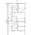
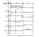
従来のアクティブマトリクス型表示装置の画素構成を図62に示す(特許文献1)。図
62に示した画素は、薄膜トランジスタ(Thin Film Transistor:
TFT)11、TFT12、容量素子13、発光素子14を有し、信号線15及び走査線
16に接続されている。なお、TFT12のソース電極もしくはドレイン電極のいずれか
一方及び容量素子13の一方の電極には電源電位Vddが供給され、発光素子14の対向
電極にはグランド電位が供給されている。The pixel configuration of the conventional active matrix type display device is shown in FIG. 62 (Patent Document 1). The pixels shown in FIG. 62 are thin film transistors (Thin Film Transistors).
It has a TFT) 11, a
このとき、発光素子に供給する電流値を制御するTFT12、即ち駆動用TFTの半導
体層にアモルファスシリコンを用いた場合、劣化等によりしきい値電圧(Vth)に変動
が生じる。この場合、異なる画素に信号線15から同じ電位を印加したにもかかわらず、
発光素子14に流れる電流は画素ごとに異なり、表示される輝度が画素によって不均一と
なる。なお、駆動用TFTの半導体層にポリシリコンを用いた場合においても、トランジ
スタの特性が劣化したり、ばらついたりする。At this time, when amorphous silicon is used for the semiconductor layer of the
The current flowing through the
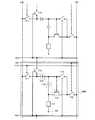
この問題を改善すべく、特許文献2において図63の画素を用いた動作方法が提案され
ている。図63に示した画素は、トランジスタ21、発光素子24に供給する電流値を制
御する駆動用トランジスタ22、容量素子23、発光素子24を有し、画素は信号線25
、走査線26に接続されている。なお、駆動用トランジスタ22はNMOSトランジスタ
であり、駆動用トランジスタ22のソース電極もしくはドレイン電極のいずれか一方には
グランド電位が供給され、発光素子24の対向電極にはVcaが供給される。In order to improve this problem,
, Is connected to the
この画素の動作におけるタイミングチャートを図64に示す。図64において、1フレ
ーム期間は、初期化期間31、しきい値電圧(Vth)書き込み期間32、データ書き込
み期間33及び発光期間34に分割される。なお、1フレーム期間とは1画面分の画像を
表示する期間に相当し、初期化期間、しきい値電圧(Vth)書き込み期間及びデータ書
き込み期間をまとめてアドレス期間と呼ぶ。The timing chart in the operation of this pixel is shown in FIG. In FIG. 64, one frame period is divided into an
まず、しきい値電圧書き込み期間32において、駆動用トランジスタ22のしきい値電
圧が容量素子に書き込まれる。その後、データ書き込み期間33において、画素の輝度を
示すデータ電圧(Vdata)が容量素子に書き込まれ、Vdata+Vthが容量素子
に蓄積される。そして、発光期間において駆動用トランジスタ22はオンとなり、Vca
を変化させることでデータ電圧によって指定された輝度で発光素子24が発光する。この
ような動作により、駆動用トランジスタのしきい値電圧の変動による輝度のばらつきを低
減している。First, in the threshold
The light emitting element 24 emits light with the brightness specified by the data voltage. By such an operation, the variation in brightness due to the variation in the threshold voltage of the drive transistor is reduced.
特許文献3においても、駆動用TFTのしきい値電圧にデータ電位を加えた電圧がゲー
ト・ソース間電圧となり、TFTのしきい値電圧が変動した場合であっても流れる電流は
変化しないことが開示されている。
上述のように表示装置では、駆動用TFTのしきい値電圧のばらつきに起因する電流値の
ばらつきを抑制することが求められていた。Also in
As described above, in the display device, it has been required to suppress the variation in the current value due to the variation in the threshold voltage of the driving TFT.
特許文献2及び3に記載されている動作方法はいずれの場合においても、Vcaの電位
を1フレーム期間当たりに数度と変化させることで上述した初期化、しきい値電圧の書き
込み、発光を行っていた。これらの画素において、Vcaが供給されている発光素子の一
方の電極、即ち対向電極は画素領域全体に形成されているため、初期化及びしきい値電圧
の書き込み以外にデータの書き込み動作を行っている画素がたとえ一つでもあると発光素
子を発光させることができない。よって、図65に示すように、1フレーム期間における
発光期間の割合(即ち、デューティー比)が小さくなってしまう。In any of the operating methods described in
デューティー比が低いと発光素子や駆動用トランジスタに流す電流値を大きくする必要
があるため、発光素子にかかる電圧が大きくなり消費電力が大きくなる。また、発光素子
や駆動用トランジスタが劣化しやすくなるため、画面の焼きつきが生じたり、劣化前と同
等の輝度を得るにはさらに大きな電力を要することになる。When the duty ratio is low, it is necessary to increase the current value to be passed through the light emitting element and the driving transistor, so that the voltage applied to the light emitting element becomes large and the power consumption becomes large. Further, since the light emitting element and the driving transistor are liable to be deteriorated, the screen is burnt, and a larger power is required to obtain the same brightness as before the deterioration.
また、対向電極は全画素接続されているため、発光素子は容量の大きい素子として機能
する。よって、対向電極の電位を変えるためには、高い消費電力が必要となる。Further, since the counter electrode is connected to all pixels, the light emitting element functions as an element having a large capacity. Therefore, high power consumption is required to change the potential of the counter electrode.
上記問題を鑑み、本発明は、消費電力が低く、明るい表示装置を提供することを課題と
する。また、データ電位によって指定された輝度からのずれが少ない画素構成、半導体装
置、及び表示装置を得ることを課題とする。なお、発光素子を有する表示装置のみが対象
となるわけではなく、本発明はトランジスタのしきい値電圧のばらつきに起因する電流値
のばらつきを抑制することを課題とする。In view of the above problems, it is an object of the present invention to provide a bright display device having low power consumption. Another object of the present invention is to obtain a pixel configuration, a semiconductor device, and a display device having a small deviation from the brightness specified by the data potential. It should be noted that the present invention is not limited to a display device having a light emitting element, and an object of the present invention is to suppress variations in the current value due to variations in the threshold voltage of the transistor.
本発明の一は、負荷に供給する電流値を制御するトランジスタと、第1の保持容量と、
第2の保持容量と、第1のスイッチ乃至第4のスイッチとを含む画素を有し、前記第2の
保持容量に前記トランジスタのしきい値電圧を保持させた後、ビデオ信号に応じた電位を
前記画素に入力する。このようにして、前記第2の保持容量に、前記しきい値電圧に前記
ビデオ信号に応じた電位のうちの前記第1の保持容量と容量分割された電位が加算された
電圧を保持させることで、トランジスタのしきい値電圧のばらつきに起因した電流値のば
らつきを抑制する。よって、発光素子をはじめとする負荷に所望の電流を供給することが
できる。また、ビデオ信号によって指定された輝度からのずれが少ない表示装置を提供す
ることが可能となる。One of the present inventions includes a transistor that controls the value of the current supplied to the load, a first holding capacitance, and the like.
It has a pixel including a second holding capacitance and a first switch to a fourth switch, and after holding the threshold voltage of the transistor in the second holding capacitance, a potential corresponding to a video signal. Is input to the pixel. In this way, the second holding capacity is made to hold a voltage obtained by adding the first holding capacity and the capacitance-divided potential of the potentials corresponding to the video signal to the threshold voltage. Therefore, the variation in the current value caused by the variation in the threshold voltage of the transistor is suppressed. Therefore, a desired current can be supplied to the load including the light emitting element. Further, it is possible to provide a display device having a small deviation from the brightness specified by the video signal.
本発明の一は、トランジスタと、保持容量と、第1のスイッチと、第2のスイッチと、
第3のスイッチと、第4のスイッチとを有し、前記トランジスタのソース電極及びドレイ
ン電極の一方は画素電極と電気的に接続され、前記トランジスタのソース電極及びドレイ
ン電極の他方は前記第2のスイッチを介して第1の配線と電気的に接続され、前記トラン
ジスタのソース電極及びドレイン電極の他方は前記第3のスイッチを介して前記トランジ
スタのゲート電極と電気的に接続され、前記トランジスタのゲート電極は、前記保持容量
及び前記第4のスイッチを介して第2の配線に電気的に接続され、前記トランジスタのゲ
ート電極は、前記保持容量及び前記第1のスイッチを介して第3の配線に電気的に接続さ
れている半導体装置である。One of the present invention is a transistor, a holding capacitance, a first switch, a second switch, and the like.
It has a third switch and a fourth switch, one of the source electrode and the drain electrode of the transistor is electrically connected to the pixel electrode, and the other of the source electrode and the drain electrode of the transistor is the second switch. The other of the source electrode and the drain electrode of the transistor is electrically connected to the gate electrode of the transistor via the third switch, and is electrically connected to the gate electrode of the transistor via a switch. The electrode is electrically connected to the second wiring via the holding capacitance and the fourth switch, and the gate electrode of the transistor is connected to the third wiring via the holding capacitance and the first switch. It is an electrically connected semiconductor device.
本発明の一は、トランジスタと、第1の保持容量と、第2の保持容量と、第1のスイッ
チと、第2のスイッチと、第3のスイッチと、第4のスイッチとを有し、前記トランジス
タのソース電極及びドレイン電極の一方は画素電極と電気的に接続され、前記トランジス
タのソース電極及びドレイン電極の一方は前記第2の保持容量を介して前記トランジスタ
のゲート電極と電気的に接続され、前記トランジスタのソース電極及びドレイン電極の他
方は前記第2のスイッチを介して第1の配線と電気的に接続され、前記トランジスタのソ
ース電極及びドレイン電極の他方は前記第3のスイッチを介して前記トランジスタのゲー
ト電極と電気的に接続され、前記トランジスタのゲート電極は、前記第1の保持容量及び
前記第4のスイッチを介して第2の配線と電気的に接続され、前記トランジスタのゲート
電極は、前記第1の保持容量及び前記第1のスイッチを介して第3の配線と電気的に接続
されている半導体装置である。One of the present invention has a transistor, a first holding capacity, a second holding capacity, a first switch, a second switch, a third switch, and a fourth switch. One of the source electrode and the drain electrode of the transistor is electrically connected to the pixel electrode, and one of the source electrode and the drain electrode of the transistor is electrically connected to the gate electrode of the transistor via the second holding capacitance. The other of the source electrode and the drain electrode of the transistor is electrically connected to the first wiring via the second switch, and the other of the source electrode and the drain electrode of the transistor is via the third switch. The gate electrode of the transistor is electrically connected to the gate electrode of the transistor, and the gate electrode of the transistor is electrically connected to the second wiring via the first holding capacitance and the fourth switch. The electrode is a semiconductor device that is electrically connected to the third wiring via the first holding capacitance and the first switch.
本発明の一は、トランジスタと、第1の保持容量と、第2の保持容量と、第1のスイッ
チと、第2のスイッチと、第3のスイッチと、第4のスイッチと、第5のスイッチとを有
し、前記トランジスタのソース電極及びドレイン電極の一方は画素電極と電気的に接続さ
れ、前記トランジスタのソース電極及びドレイン電極の一方は前記第2の保持容量を介し
て前記トランジスタのゲート電極と電気的に接続され、前記トランジスタのソース電極及
びドレイン電極の一方は第5のスイッチを介して第4の配線と電気的に接続され、前記ト
ランジスタのソース電極及びドレイン電極の他方は前記第2のスイッチを介して第1の配
線と電気的に接続され、前記トランジスタのソース電極及びドレイン電極の他方は前記第
3のスイッチを介して前記トランジスタのゲート電極と電気的に接続され、前記トランジ
スタのゲート電極は、前記第1の保持容量及び前記第4のスイッチを介して第2の配線に
電気的に接続され、前記トランジスタのゲート電極は、前記第1の保持容量及び前記第1
のスイッチを介して第3の配線に電気的に接続されている半導体装置である。One of the present invention is a transistor, a first holding capacity, a second holding capacity, a first switch, a second switch, a third switch, a fourth switch, and a fifth. It has a switch, one of the source electrode and the drain electrode of the transistor is electrically connected to the pixel electrode, and one of the source electrode and the drain electrode of the transistor is the gate of the transistor via the second holding capacitance. It is electrically connected to the electrode, one of the source electrode and the drain electrode of the transistor is electrically connected to the fourth wiring via the fifth switch, and the other of the source electrode and the drain electrode of the transistor is the first. The other of the source electrode and the drain electrode of the transistor is electrically connected to the gate electrode of the transistor via the third switch, and is electrically connected to the first wiring via the switch of 2. The gate electrode of the transistor is electrically connected to the second wiring via the first holding capacitance and the fourth switch, and the gate electrode of the transistor has the first holding capacitance and the first holding capacitance.
It is a semiconductor device that is electrically connected to the third wiring via the switch of.
上記構成において、前記第2の配線は第1のスイッチを制御する配線と同一であること
を特徴としても良い。また、前記第2の配線は前行もしくは次行の第1のスイッチ乃至第
4のスイッチを制御する走査線のいずれかであっても良い。In the above configuration, the second wiring may be the same as the wiring that controls the first switch. Further, the second wiring may be either a scanning line for controlling the first switch to the fourth switch in the previous line or the next line.
本発明の一は、トランジスタと、第1の保持容量と、第2の保持容量と、第1のスイッ
チと、第2のスイッチと、第3のスイッチと、第4のスイッチとを有し、前記トランジス
タのソース電極及びドレイン電極の一方は画素電極と電気的に接続され、前記トランジス
タのソース電極及びドレイン電極の一方は前記第2の保持容量を介して前記トランジスタ
のゲート電極と電気的に接続され、前記トランジスタのソース電極及びドレイン電極の他
方は前記第2のスイッチを介して第1の配線と電気的に接続され、前記トランジスタのソ
ース電極及びドレイン電極の他方は前記第3のスイッチを介して前記トランジスタのゲー
ト電極と電気的に接続され、前記トランジスタのゲート電極は、前記第1の保持容量及び
前記第4のスイッチを介して前記第1の配線と電気的に接続され、前記トランジスタのゲ
ート電極は、前記第1の保持容量及び前記第1のスイッチを介して第3の配線と電気的に
接続されている半導体装置である。One of the present invention has a transistor, a first holding capacity, a second holding capacity, a first switch, a second switch, a third switch, and a fourth switch. One of the source electrode and the drain electrode of the transistor is electrically connected to the pixel electrode, and one of the source electrode and the drain electrode of the transistor is electrically connected to the gate electrode of the transistor via the second holding capacitance. The other of the source electrode and the drain electrode of the transistor is electrically connected to the first wiring via the second switch, and the other of the source electrode and the drain electrode of the transistor is via the third switch. The gate electrode of the transistor is electrically connected to the gate electrode of the transistor, and the gate electrode of the transistor is electrically connected to the first wiring via the first holding capacitance and the fourth switch of the transistor. The gate electrode is a semiconductor device that is electrically connected to a third wiring via the first holding capacitance and the first switch.
本発明の一は、トランジスタと、第1の保持容量と、第2の保持容量と、第1のスイッ
チと、第2のスイッチと、第3のスイッチと、整流素子とを有し、前記トランジスタのソ
ース電極及びドレイン電極の一方は画素電極と電気的に接続され、前記トランジスタのソ
ース電極及びドレイン電極の一方は前記第2の保持容量を介して前記トランジスタのゲー
ト電極と電気的に接続され、前記トランジスタのソース電極及びドレイン電極の他方は前
記第2のスイッチを介して第1の配線と電気的に接続され、前記トランジスタのソース電
極及びドレイン電極の他方は前記第3のスイッチを介して前記トランジスタのゲート電極
と電気的に接続され、前記トランジスタのゲート電極は、前記第1の保持容量及び前記整
流素子を介して第2の配線に電気的に接続され、前記トランジスタのゲート電極は、前記
第1の保持容量及び前記第1のスイッチを介して第3の配線に電気的に接続されている半
導体装置である。One of the present invention includes a transistor, a first holding capacity, a second holding capacity, a first switch, a second switch, a third switch, and a rectifying element. One of the source electrode and the drain electrode of the transistor is electrically connected to the pixel electrode, and one of the source electrode and the drain electrode of the transistor is electrically connected to the gate electrode of the transistor via the second holding capacitance. The other of the source electrode and drain electrode of the transistor is electrically connected to the first wiring via the second switch, and the other of the source electrode and drain electrode of the transistor is said via the third switch. It is electrically connected to the gate electrode of the transistor, the gate electrode of the transistor is electrically connected to the second wiring via the first holding capacitance and the rectifying element, and the gate electrode of the transistor is said. It is a semiconductor device that is electrically connected to a third wiring via a first holding capacity and the first switch.
本発明の一は、トランジスタと、第1の保持容量と、第2の保持容量と、第1のスイッ
チと、第2のスイッチと、第3のスイッチと、第4のスイッチとを有し、前記トランジス
タのソース電極及びドレイン電極の一方は画素電極と電気的に接続され、前記トランジス
タのソース電極及びドレイン電極の一方は前記第2の保持容量を介して前記トランジスタ
のゲート電極と電気的に接続され、前記トランジスタのソース電極及びドレイン電極の他
方は前記第2のスイッチを介して第1の配線と電気的に接続され、前記トランジスタのソ
ース電極及びドレイン電極の他方は前記第3のスイッチを介して前記トランジスタのゲー
ト電極と電気的に接続され、前記トランジスタのゲート電極は、前記第1の保持容量及び
前記第1のスイッチを介して第3の配線に電気的に接続され、前記第4のスイッチは前記
第1の保持容量と並列に電気的に接続され、なおかつ前記第1のスイッチを介して前記第
3の配線に電気的に接続されている半導体装置である。One of the present invention has a transistor, a first holding capacity, a second holding capacity, a first switch, a second switch, a third switch, and a fourth switch. One of the source electrode and the drain electrode of the transistor is electrically connected to the pixel electrode, and one of the source electrode and the drain electrode of the transistor is electrically connected to the gate electrode of the transistor via the second holding capacitance. The other of the source electrode and the drain electrode of the transistor is electrically connected to the first wiring via the second switch, and the other of the source electrode and the drain electrode of the transistor is via the third switch. The gate electrode of the transistor is electrically connected to the gate electrode of the transistor, and the gate electrode of the transistor is electrically connected to the third wiring via the first holding capacitance and the first switch. The switch is a semiconductor device that is electrically connected in parallel with the first holding capacitance and is also electrically connected to the third wiring via the first switch.
前記トランジスタは、Nチャネル型トランジスタであってもよい。また、前記トランジ
スタの半導体層は、非晶質半導体膜からなることを特徴としてもよい。さらに、前記トラ
ンジスタの半導体層は、アモルファスシリコンからなることを特徴としてもよい。The transistor may be an N-channel type transistor. Further, the semiconductor layer of the transistor may be characterized in that it is made of an amorphous semiconductor film. Further, the semiconductor layer of the transistor may be characterized in that it is made of amorphous silicon.
また、前記トランジスタの半導体層は、結晶性半導体膜からなることを特徴としてもよ
い。Further, the semiconductor layer of the transistor may be characterized in that it is made of a crystalline semiconductor film.
上記発明において、前記第1の配線の電位は、前記画素電極の電位に前記トランジスタ
のしきい値電圧を加算した値より高いことを特徴しても良い。In the above invention, the potential of the first wiring may be higher than the value obtained by adding the threshold voltage of the transistor to the potential of the pixel electrode.
また、前記トランジスタは、Pチャネル型トランジスタであってもよい。その場合、上
記発明において、前記第1の配線の電位は、前記画素電極の電位から前記トランジスタの
しきい値電圧を減算した値より低いことを特徴としても良い。Further, the transistor may be a P-channel type transistor. In that case, in the above invention, the potential of the first wiring may be lower than the value obtained by subtracting the threshold voltage of the transistor from the potential of the pixel electrode.
本発明の一は、第1の保持容量と、ソース電極及びドレイン電極の一方が負荷に電気的
に接続され、ソース電極及びドレイン電極の他方が第1の配線に電気的に接続され、ゲー
ト電極が前記第1の保持容量を介して第2の配線と電気的に接続されるトランジスタと、
前記トランジスタのゲートソース間電圧を保持する第2の保持容量と、前記第1の保持容
量に第1の電圧を、前記第2の保持容量に第2の電圧を保持させる手段と、前記第2の保
持容量の第2の電圧を前記トランジスタのしきい値電圧まで放電させる手段と、前記第2
の配線からビデオ信号に応じた電位を前記第1の保持容量に入力することにより前記トラ
ンジスタに設定された電流を前記負荷に供給する手段とを有することを特徴とする半導体
装置である。One of the present inventions is that the first holding capacity and one of the source electrode and the drain electrode are electrically connected to the load, the other of the source electrode and the drain electrode is electrically connected to the first wiring, and the gate electrode. Is a transistor that is electrically connected to the second wiring via the first holding capacitance.
A second holding capacitance for holding the gate-source voltage of the transistor, a means for holding the first voltage in the first holding capacitance, and a second voltage in the second holding capacitance, and the second holding capacitance. A means for discharging the second voltage of the holding capacity of the transistor to the threshold voltage of the transistor, and the second voltage.
The semiconductor device is characterized by having a means for supplying a current set in the transistor to the load by inputting a potential corresponding to a video signal from the wiring of the above to the first holding capacitance.
前記トランジスタは、Nチャネル型トランジスタであってもよい。また、前記トランジ
スタの半導体層は、非晶質半導体膜からなることを特徴としてもよい。さらに、前記トラ
ンジスタの半導体層は、アモルファスシリコンからなることを特徴としてもよい。The transistor may be an N-channel type transistor. Further, the semiconductor layer of the transistor may be characterized in that it is made of an amorphous semiconductor film. Further, the semiconductor layer of the transistor may be characterized in that it is made of amorphous silicon.
また、前記トランジスタの半導体層は、結晶性半導体膜からなることを特徴としてもよ
い。Further, the semiconductor layer of the transistor may be characterized in that it is made of a crystalline semiconductor film.
また、前記トランジスタは、Pチャネル型トランジスタであってもよい。 Further, the transistor may be a P-channel type transistor.
また、本発明の一は、上記に記載した半導体装置を有する表示装置である。また、前記
表示装置を有する電子機器である。Further, one of the present inventions is a display device having the semiconductor device described above. Further, it is an electronic device having the display device.
なお、明細書に示すスイッチは、様々な形態のものを用いることができる。例としては
、電気的スイッチや機械的なスイッチなどがある。つまり、電流の流れを制御できるもの
であればよく、特定のものに限定されない。例えば、スイッチとして、トランジスタ(例
えば、バイポーラトランジスタ、MOSトランジスタなど)、ダイオード(例えば、PN
ダイオード、PINダイオード、ショットキーダイオード、MIM(Metal Ins
ulator Metal)ダイオード、MIS(Metal Insulator S
emiconductor)ダイオード、ダイオード接続のトランジスタなど)、サイリ
スタなどを用いることが出来る。また、これらを組み合わせた論理回路をスイッチとして
用いることも可能である。As the switch shown in the specification, various forms can be used. Examples include electrical switches and mechanical switches. That is, it is not limited to a specific one as long as it can control the flow of electric current. For example, as a switch, a transistor (for example, a bipolar transistor, a MOS transistor, etc.), a diode (for example, a PN)
Diode, PIN diode, Schottky diode, MIM (Metal Ins)
ulator Metal diode, MIS (Metal Insulator S)
(Emiconductor) diode, diode-connected transistor, etc.), thyristor, etc. can be used. It is also possible to use a logic circuit that combines these as a switch.
スイッチとしてトランジスタを用いる場合、そのトランジスタは、単なるスイッチとし
て動作するため、トランジスタの極性(導電型)は特に限定されない。ただし、オフ電流
が少ない方の極性のトランジスタを用いることが望ましい。オフ電流が少ないトランジス
タとしては、LDD領域を有するトランジスタやマルチゲート構造を有するトランジスタ
等がある。また、スイッチとして動作させるトランジスタのソース電極の電位が、低電位
側電源(Vss、GND、0Vなど)に近い状態で動作する場合はNチャネル型を、反対
にソース電極の電位が高電位側電源(Vddなど)に近い状態で動作する場合はPチャネ
ル型のトランジスタを用いることが望ましい。このように動作させることで、ゲートソー
ス間電圧の絶対値を大きくできるため、スイッチとしての動作がより容易になる。また、
ソースフォロワ動作をしてしまうことが少ないため、出力電圧の大きさが小さくなること
を防止することができる。When a transistor is used as a switch, the polarity (conductive type) of the transistor is not particularly limited because the transistor operates as a mere switch. However, it is desirable to use a transistor with the polarity with the smaller off current. Examples of the transistor having a small off-current include a transistor having an LDD region and a transistor having a multi-gate structure. If the potential of the source electrode of the transistor to be operated as a switch is close to the low potential side power supply (Vss, GND, 0V, etc.), the N channel type is used. On the contrary, the source electrode potential is the high potential side power supply. It is desirable to use a P-channel type transistor when operating in a state close to (Vdd, etc.). By operating in this way, the absolute value of the voltage between the gate and source can be increased, so that the operation as a switch becomes easier. Also,
Since the source follower operation is unlikely to occur, it is possible to prevent the magnitude of the output voltage from becoming small.
なお、Nチャネル型トランジスタとPチャネル型トランジスタの両方を用いて、CMO
S型のスイッチをスイッチとして用いてもよい。CMOS型のスイッチにすると、様々な
入力電圧に対し出力電圧を制御しやすいため、適切な動作を行うことができる。さらに、
スイッチをオン・オフさせるための信号の電圧振幅値を小さくすることができるため、消
費電力を低減することも可能である。CMO using both N-channel transistor and P-channel transistor
An S-type switch may be used as a switch. When a CMOS type switch is used, it is easy to control the output voltage for various input voltages, so that appropriate operation can be performed. further,
Since the voltage amplitude value of the signal for turning the switch on and off can be reduced, it is also possible to reduce the power consumption.
なお、スイッチとしてトランジスタを用いる場合、ソース電極及びドレイン電極の一方
がスイッチの入力端子として、ソース電極及びドレイン電極の他方が出力端子として、ゲ
ート電極がスイッチの導通を制御する端子として機能する。一方、スイッチとしてダイオ
ードを用いる場合、スイッチは、導通を制御する端子を有していない場合がある。そのた
め、スイッチとしてトランジスタよりダイオードを用いた方が、端子を制御するための配
線が不要なため、配線数を少なくすることができる。When a transistor is used as the switch, one of the source electrode and the drain electrode functions as an input terminal of the switch, the other of the source electrode and the drain electrode functions as an output terminal, and the gate electrode functions as a terminal for controlling the conduction of the switch. On the other hand, when a diode is used as the switch, the switch may not have a terminal for controlling conduction. Therefore, when a diode is used as a switch rather than a transistor, wiring for controlling terminals is not required, and the number of wirings can be reduced.
なお、本発明において接続されているとは、電気的に接続されていることと同義である
。したがって、本発明が開示する構成において、所定の接続関係、例えば図または文章に
示された接続関係に加え、その間に電気的な接続を可能とする他の素子(例えば、スイッ
チやトランジスタや容量素子やインダクタや抵抗素子やダイオードなど)が配置されてい
てもよい。もちろん、間に他の素子を介さずに配置されていてもよく、電気的に接続され
ているとは直接的に接続されている場合を含むものとする。
なお、負荷はエレクトロルミネセンス素子に代表される発光素子に限定されず、電流が流
れることにより明るさ、色調、偏光などが変化する表示媒体を適用することができる。そ
の他、所望の電流を負荷に供給することができれば良いため、負荷には例えば電子放出素
子、液晶素子、電子インク、電気泳動素子、グレーティングライトバルブ(GLV)、プ
ラズマディスプレイ(PDP)、デジタルマイクロミラーデバイス(DMD)など磁気的
作用によりコントラストが変化する表示媒体なども適用することができる。また、電子放
出素子にカーボンナノチューブを利用することも可能である。なお、EL素子を用いた表
示装置としてはELディスプレイ、電子放出素子を用いた表示装置としてはフィールドエ
ミッションディスプレイ(FED)やSED方式平面型ディスプレイ(SED:Surf
ace−conduction Electron−emitter Disply)な
どが挙げられる。また、液晶素子を用いた表示装置としては液晶ディスプレイ、透過型液
晶ディスプレイ、半透過型液晶ディスプレイや反射型液晶ディスプレイが、電子インクを
用いた表示装置としては電子ペーパーがある。In the present invention, being connected is synonymous with being electrically connected. Therefore, in the configuration disclosed by the present invention, in addition to the predetermined connection relationship, for example, the connection relationship shown in the figure or text, other elements (for example, a switch, a transistor, or a capacitive element) that enable an electrical connection between them. , Inductors, resistance elements, diodes, etc.) may be arranged. Of course, it may be arranged without interposing another element between them, and the case of being electrically connected includes the case of being directly connected.
The load is not limited to a light emitting element typified by an electroluminescence element, and a display medium whose brightness, color tone, polarization, etc. change due to the flow of an electric current can be applied. In addition, since it is sufficient that a desired current can be supplied to the load, the load includes, for example, an electron emitting element, a liquid crystal element, an electronic ink, an electrophoresis element, a grating light valve (GLV), a plasma display (PDP), and a digital micromirror. A display medium or the like whose contrast changes due to a magnetic action such as a device (DMD) can also be applied. It is also possible to use carbon nanotubes for the electron emitting element. The display device using the EL element is an EL display, and the display device using an electron emitting element is a field emission display (FED) or an SED flat display (SED: Surf).
ace-conduction Electron-emitter Display) and the like can be mentioned. Further, as a display device using a liquid crystal element, there are a liquid crystal display, a transmissive liquid crystal display, a transflective liquid crystal display and a reflective liquid crystal display, and as a display device using electronic ink, there is electronic paper.
なお、トランジスタとは、ゲート電極と、ドレイン領域と、ソース領域とを含む少なく
とも三つの端子を有する素子であり、ドレイン領域とソース領域の間にチャネル形成領域
を有する。ここで、ソース領域とドレイン領域とは、トランジスタの構造や動作条件等に
よって変わるため、ソース領域またはドレイン領域の範囲を正確に限定することが困難で
ある。そこで、トランジスタの接続関係を説明する際には、ドレイン領域とソース領域の
2端子についてはこれらの領域に接続された電極の一方を第1の電極、他方を第2の電極
と表記し、説明に用いる。The transistor is an element having at least three terminals including a gate electrode, a drain region, and a source region, and has a channel forming region between the drain region and the source region. Here, since the source region and the drain region change depending on the structure of the transistor, operating conditions, and the like, it is difficult to accurately limit the range of the source region or the drain region. Therefore, when explaining the connection relationship of the transistors, regarding the two terminals of the drain region and the source region, one of the electrodes connected to these regions is referred to as a first electrode and the other is referred to as a second electrode. Used for.
なお、トランジスタは、ベースとエミッタとコレクタとを含む少なくとも三つの端子を
有する素子であってもよく、エミッタとコレクタのいずれか一方が第1の電極、他方が第
2の電極に相当する。The transistor may be an element having at least three terminals including a base, an emitter and a collector, and one of the emitter and the collector corresponds to a first electrode and the other corresponds to a second electrode.
本発明において、トランジスタは、様々な形態のトランジスタを適用させることができ
、種類に特に限定はない。例えば、非晶質シリコン、多結晶シリコン、微結晶(マイクロ
クリスタル、セミアモルファスとも言う)シリコンなどに代表される非単結晶半導体膜を
有する薄膜トランジスタ(TFT)などを用いることができる。TFTを用いる場合、様
々なメリットがある。例えば、単結晶シリコンの場合よりも低い温度で製造できるため、
製造コストの削減や製造装置の大型化を図ることができる。製造装置の大型化が可能とな
ることで、大型基板上に製造でき、同時に多くの個数の表示装置を製造できる。よって、
さらに低コストで製造することが可能となる。また、製造温度が低いため、耐熱性の弱い
基板を用いることもでき、例えばガラス基板等の透光性を有する基板上にトランジスタを
製造できる。In the present invention, various forms of transistors can be applied to the transistors, and the types are not particularly limited. For example, a thin film transistor (TFT) having a non-single crystal semiconductor film typified by amorphous silicon, polycrystalline silicon, microcrystal (also referred to as microcrystal or semi-amorphous) silicon, or the like can be used. When using a TFT, there are various merits. For example, because it can be manufactured at a lower temperature than single crystal silicon.
It is possible to reduce the manufacturing cost and increase the size of the manufacturing equipment. Since the size of the manufacturing device can be increased, it can be manufactured on a large substrate, and a large number of display devices can be manufactured at the same time. Therefore,
It can be manufactured at a lower cost. Further, since the manufacturing temperature is low, a substrate having weak heat resistance can be used, and a transistor can be manufactured on a translucent substrate such as a glass substrate.
なお、多結晶シリコンを製造する際、触媒(ニッケルなど)を用いることにより結晶性
をさらに向上させ、電気特性のよいトランジスタを製造することが可能となる。その結果
、ゲートドライバ回路(走査線駆動回路)やソースドライバ回路(信号線駆動回路)、信
号処理回路(信号生成回路、ガンマ補正回路、DA変換回路など)を基板上に一体形成す
ることが可能となる。なお、必ずしも触媒を用いる必要はない。When producing polycrystalline silicon, the crystallinity can be further improved by using a catalyst (nickel or the like), and a transistor having good electrical characteristics can be produced. As a result, a gate driver circuit (scanning line drive circuit), a source driver circuit (signal line drive circuit), and a signal processing circuit (signal generation circuit, gamma correction circuit, DA conversion circuit, etc.) can be integrally formed on the substrate. It becomes. It is not always necessary to use a catalyst.
また、微結晶シリコンを用いた際にも、ゲートドライバ回路(走査線駆動回路)やソー
スドライバ回路の一部(アナログスイッチなど)を基板上に一体形成することが出来る。Further, even when microcrystalline silicon is used, a part of the gate driver circuit (scanning line drive circuit) and a part of the source driver circuit (analog switch, etc.) can be integrally formed on the substrate.
また、半導体基板やSOI基板などを用いてトランジスタを形成することが出来る。そ
の場合、MOS型トランジスタ、接合型トランジスタ、バイポーラトランジスタなどをト
ランジスタとして用いることが出来る。これらにより、特性、サイズや形状などのバラツ
キが少なく、電流供給能力が高いトランジスタを製造することができる。よって、回路の
低消費電力化、回路の高集積化等を図ることができる。Further, a transistor can be formed by using a semiconductor substrate, an SOI substrate, or the like. In that case, a MOS transistor, a junction transistor, a bipolar transistor, or the like can be used as the transistor. As a result, it is possible to manufacture a transistor having a high current supply capacity with little variation in characteristics, size, shape, and the like. Therefore, it is possible to reduce the power consumption of the circuit, increase the integration of the circuit, and the like.
また、ZnO、a−InGaZnO、SiGe、GaAs、IZO、ITO、SnOな
どの化合物半導体または酸化物半導体を有するトランジスタや、さらにこれらの化合物半
導体または酸化物半導体を薄膜化した薄膜トランジスタなどを用いることが出来る。これ
らにより、製造温度を低くでき、例えば室温でトランジスタを製造することが可能となる
。その結果、耐熱性の低い基板、例えばプラスチック基板やフィルム基板に直接トランジ
スタを形成することができる。なお、これらの化合物半導体または酸化物半導体を、トラ
ンジスタのチャネル部分に用いるだけでなく、それ以外の用途で用いることも出来る。例
えば、これらの化合物半導体または酸化物半導体を抵抗素子、画素電極、透明電極として
用いることができる。さらに、これらをトランジスタと同時に成膜又は形成できるため、
コストを低減することができる。Further, a transistor having a compound semiconductor or an oxide semiconductor such as ZnO, a-InGaZnO, SiGe, GaAs, IZO, ITO, SnO, and a thin film transistor obtained by thinning these compound semiconductors or oxide semiconductors can be used. .. As a result, the manufacturing temperature can be lowered, and for example, a transistor can be manufactured at room temperature. As a result, the transistor can be formed directly on a substrate having low heat resistance, for example, a plastic substrate or a film substrate. It should be noted that these compound semiconductors or oxide semiconductors can be used not only for the channel portion of the transistor but also for other purposes. For example, these compound semiconductors or oxide semiconductors can be used as resistance elements, pixel electrodes, and transparent electrodes. Furthermore, since these can be formed or formed at the same time as the transistor,
The cost can be reduced.
また、インクジェットや印刷法を用いて形成したトランジスタなども用いることができ
る。これにより、室温で製造、低真空度で製造、又は大型基板上に製造することができる
。また、マスク(レチクル)を用いずに製造することが可能となるため、トランジスタの
レイアウトを容易に変更することができる。さらに、レジストを用いる必要がないため、
工程数が削減され、製造コストを低減することができる。また、必要な部分にのみ成膜す
るため、全面に成膜した後にエッチングする場合に比べ材料が無駄にならず低コストで作
製することが可能となる。Further, a transistor formed by using an inkjet or a printing method can also be used. As a result, it can be manufactured at room temperature, at a low degree of vacuum, or on a large substrate. Further, since it can be manufactured without using a mask (reticle), the layout of the transistor can be easily changed. Furthermore, since it is not necessary to use a resist,
The number of processes can be reduced and the manufacturing cost can be reduced. Further, since the film is formed only on the necessary portion, the material is not wasted and the film can be produced at low cost as compared with the case where the film is formed on the entire surface and then etched.
また、有機半導体やカーボンナノチューブを有するトランジスタ等を用いることができ
る。このようなトランジスタはフレキシブルな基板にも設けることが可能であるため、衝
撃耐性に優れている。これらに限らず、その他様々なトランジスタを用いることができる
。Further, an organic semiconductor, a transistor having carbon nanotubes, or the like can be used. Since such a transistor can be provided on a flexible substrate, it has excellent impact resistance. Not limited to these, various other transistors can be used.
なお、トランジスタが形成されている基板の種類においても、様々なものを用いること
ができ、特定のものに限定されることはない。トランジスタが形成される基板としては、
例えば、単結晶基板、SOI基板、ガラス基板、石英基板、プラスチック基板、紙基板、
セロファン基板、石材基板、木材基板、布基板(天然繊維(絹、綿、麻)、合成繊維(ナ
イロン、ポリウレタン、ポリエステル)若しくは再生繊維(アセテート、キュプラ、レー
ヨン、再生ポリエステル)などを含む)、ゴム基板、ステンレス・スチル基板、ステンレ
ス・スチル・ホイルを有する基板などを用いることができる。また、ある基板でトランジ
スタを形成し、その後、他の基板にトランジスタを転置し、別の基板上にトランジスタを
配置してもよい。トランジスタが転置される基板としては、単結晶基板、SOI基板、ガ
ラス基板、石英基板、プラスチック基板、紙基板、セロファン基板、石材基板、、木材基
板、布基板(天然繊維(絹、綿、麻)、合成繊維(ナイロン、ポリウレタン、ポリエステ
ル)若しくは再生繊維(アセテート、キュプラ、レーヨン、再生ポリエステル)などを含
む)、皮革基板、ゴム基板、ステンレス・スチル基板、ステンレス・スチル・ホイルを有
する基板などを用いることができる。これらの基板を用いることにより、より特性の高い
トランジスタの形成、耐熱性の向上や軽量化を図ることができる。It should be noted that various types of substrates on which transistors are formed can also be used and are not limited to specific ones. As a substrate on which a transistor is formed,
For example, single crystal substrate, SOI substrate, glass substrate, quartz substrate, plastic substrate, paper substrate,
Cellophane substrate, stone substrate, wood substrate, cloth substrate (including natural fiber (silk, cotton, linen), synthetic fiber (nylon, polyurethane, polyester) or recycled fiber (including acetate, cupra, rayon, recycled polyester)), rubber A substrate, a stainless steel substrate, a substrate having a stainless steel still foil, or the like can be used. Alternatively, a transistor may be formed on one substrate, then the transistor may be transposed on another substrate, and the transistor may be arranged on another substrate. The substrates on which the transistors are translocated include single crystal substrates, SOI substrates, glass substrates, quartz substrates, plastic substrates, paper substrates, cellophane substrates, stone substrates, wood substrates, and cloth substrates (natural fibers (silk, cotton, linen)). , Synthetic fibers (including nylon, polyurethane, polyester) or recycled fibers (including acetate, cupra, rayon, recycled polyester), leather substrates, rubber substrates, stainless steel substrates, substrates with stainless steel foil, etc. are used. be able to. By using these substrates, it is possible to form a transistor having higher characteristics, improve heat resistance, and reduce the weight.
なお、トランジスタの構成は、様々な形態をとることができ、特定の構成に限定されな
い。例えば、ゲート電極が2個以上のマルチゲート構造を用いてもよい。マルチゲート構
造にすると、チャネル領域が直列に接続されるため、複数のトランジスタが直列に接続さ
れた構成となる。このようなマルチゲート構造により、オフ電流の低減及びトランジスタ
の耐圧向上によりトランジスタの信頼性をより優れたものとすることができる。また、マ
ルチゲート構造により、飽和領域で動作する際、ドレイン・ソース間電圧が変化してもド
レイン・ソース間電流があまり変化せず、傾きがフラットな電圧−電流特性を得ることが
できる。傾きがフラットな電圧−電流特性を利用すると、理想的な電流源回路や、非常に
高い抵抗値をもつ能動負荷を実現することができる。その結果、特性の良い差動回路やカ
レントミラー回路を実現することが出来る。また、チャネル領域の上下にゲート電極が配
置されている構造でもよい。チャネル領域の上下にゲート電極を配置することにより、実
効的なチャネル領域が増えるため、電流量の増加や空乏層ができやすくなることによるS
値の低減を図ることができる。なお、チャネル領域の上下にゲート電極が配置した場合、
複数のトランジスタが並列に接続されたような構成となる。The configuration of the transistor can take various forms and is not limited to a specific configuration. For example, a multi-gate structure having two or more gate electrodes may be used. In the multi-gate structure, since the channel regions are connected in series, a plurality of transistors are connected in series. With such a multi-gate structure, the reliability of the transistor can be further improved by reducing the off-current and improving the withstand voltage of the transistor. Further, due to the multi-gate structure, when operating in the saturation region, the drain-source current does not change much even if the drain-source voltage changes, and a voltage-current characteristic with a flat slope can be obtained. By utilizing the voltage-current characteristic with a flat slope, an ideal current source circuit and an active load with a very high resistance value can be realized. As a result, a differential circuit or a current mirror circuit having good characteristics can be realized. Further, the structure may be such that gate electrodes are arranged above and below the channel region. By arranging the gate electrodes above and below the channel region, the effective channel region increases, so that the amount of current increases and the depletion layer is likely to form.
The value can be reduced. If the gate electrodes are placed above and below the channel area,
The configuration is such that a plurality of transistors are connected in parallel.
また、チャネル領域の上にゲート電極が配置されている構造でもよいし、チャネル領域
の下にゲート電極が配置されている構造でもよい。あるいは、正スタガ構造または逆スタ
ガ構造でもよい。また、チャネル領域が複数の領域に分かれていたり、チャネル領域が並
列もしくは直列に接続されていてもよい。さらに、チャネル領域(もしくはその一部)に
ソース電極やドレイン電極が重なっていてもよい。このようにチャネル領域(もしくはそ
の一部)にソース電極やドレイン電極が重なる構造とすることにより、チャネル領域の一
部に電荷がたまり、動作が不安定となることを防ぐことができる。また、LDD領域を設
けても良い。LDD領域を設けることにより、オフ電流の低減及びトランジスタの耐圧向
上によりトランジスタの信頼性をより優れたものとすることができる。あるいは、LDD
領域を設けることにより、飽和領域で動作する際、ドレイン・ソース間電圧が変化しても
、ドレイン・ソース間電流があまり変化せず傾きがフラットな電圧−電流特性を得ること
ができる。Further, the structure may be such that the gate electrode is arranged above the channel region, or the gate electrode may be arranged below the channel region. Alternatively, it may have a normal stagger structure or a reverse stagger structure. Further, the channel area may be divided into a plurality of areas, or the channel areas may be connected in parallel or in series. Further, the source electrode and the drain electrode may overlap the channel region (or a part thereof). By forming the structure in which the source electrode and the drain electrode overlap the channel region (or a part thereof) in this way, it is possible to prevent the operation from becoming unstable due to the accumulation of electric charges in a part of the channel region. Moreover, the LDD area may be provided. By providing the LDD region, the reliability of the transistor can be further improved by reducing the off-current and improving the withstand voltage of the transistor. Alternatively, LDD
By providing the region, it is possible to obtain a voltage-current characteristic in which the drain-source current does not change so much and the slope is flat even if the drain-source voltage changes when operating in the saturated region.
なお、上述したように、本発明におけるトランジスタは、様々なタイプのトランジスタ
を用いることができ、さらに様々な基板上に形成させることができる。したがって、所定
の機能を実現させるために必要な回路の全てが、同一の基板に形成されていてもよい。例
えば、所定の機能を実現させるために必要な回路の全てがガラス基板、プラスチック基板
、単結晶基板、またはSOI基板上に形成されていてもよい。このように所定の機能を実
現させるために必要な回路の全てが同じ基板上に形成することで、部品点数の削減による
コストの低減や回路部品との接続点数の低減による信頼性の向上を図ることができる。一
方、所定の機能を実現させるために必要な回路の一部をある基板に、所定の機能を実現さ
せるために必要な回路の別の一部を他の基板に形成してもよい。つまり、所定の機能を実
現させるために必要な回路の全てが同じ基板上に形成する必要はない。As described above, the transistors in the present invention can use various types of transistors and can be formed on various substrates. Therefore, all the circuits necessary for realizing a predetermined function may be formed on the same substrate. For example, all of the circuits required to realize a predetermined function may be formed on a glass substrate, a plastic substrate, a single crystal substrate, or an SOI substrate. By forming all the circuits necessary to realize a predetermined function on the same board in this way, the cost is reduced by reducing the number of parts and the reliability is improved by reducing the number of connection points with circuit parts. be able to. On the other hand, a part of the circuit necessary for realizing the predetermined function may be formed on a certain substrate, and another part of the circuit necessary for realizing the predetermined function may be formed on another substrate. That is, it is not necessary to form all the circuits necessary for realizing a predetermined function on the same substrate.
例えば、所定の機能を実現させるために必要な回路の一部をガラス基板上に、別の一部
を単結晶基板上に形成し、このように単結晶基板上のトランジスタで構成されたICチッ
プをCOG(Chip On Glass)でガラス基板に接続してガラス基板上に配置
してもよい。あるいは、そのICチップをTAB(Tape Automated Bo
nding)やプリント基板を用いてガラス基板と接続してもよい。このように、回路の
一部が同じ基板に形成されていることにより、部品点数の削減によるコストの低減や回路
部品との接続点数の低減による信頼性の向上を図ることができる。また、駆動電圧が高い
部分や駆動周波数が高い部分の回路は消費電力が大きいため、このような部分の回路は他
の回路と同じ基板に形成せず、例えば単結晶基板上に形成したICチップを用いることで
消費電力の増加を防ぐことができる。
なお、本明細書において、一画素とは明るさを制御できる要素一つ分を示すものとする。
一例としては、一画素は一つの色要素を示すものとし、その色要素一つで明るさを表現す
る。従って、そのときは、R(赤)G(緑)B(青)の色要素からなるカラー表示装置の
場合には、画像の最小単位は、Rの画素とGの画素とBの画素との三画素から構成される
ものとする。なお、色要素は、三色に限定されず、三色以上を用いても良いし、RGB以
外の色を用いても良い。例えば、RGBW(Wは白)やRGBに、例えばイエロー、シア
ン、マゼンタ、エメラルドグリーン、朱色などを一色以上追加したものなどがある。また
、RGBの中の少なくとも一色に類似した色を、RGBに追加してもよい。例えば、R、
G、B1、B2としてもよい。B1とB2は、いずれも青色であるが、周波数が多少異な
っている。同様に、R1、R2、G、BやR、G1、G2、Bとしてもよい。このような
色要素を用いることにより、より実物に近い表示を行うことができる。また、このような
色要素を用いることにより、消費電力を低減することが出来る。また、別の例としては、
1つの色要素について複数の領域を用いて明るさを制御する場合は、その領域一つ分を一
画素としてもよい。一例として、面積階調を行う場合または副画素(サブ画素)を有して
いる場合が挙げあられる。このような場合、一つの色要素につき明るさを制御する領域が
複数あり、その全体で階調を表現するわけであるが、明るさを制御する領域の一つ分を一
画素としてもよく、この場合一つの色要素は複数の画素で構成されることとなる。また、
明るさを制御する領域が1つの色要素の中に複数あっても、それらをまとめて、1つの色
要素を1画素としてもよい。なお、その場合には一つの色要素で一つの画素を構成するこ
ととなる。また、1つの色要素について、複数の領域を用いて明るさを制御する場合、画
素によって表示に寄与する領域の大きさが異なっている場合がある。また、一つの色要素
につき複数ある、明るさを制御する領域において、各々に供給する信号を僅かに異ならせ
るようにして、視野角を広げるようにしてもよい。つまり、1つの色要素について複数あ
る領域が有する画素電極の電位を各々異なるものとすることで液晶分子に加わる電圧を異
らせ、視野角を向上することもできる。For example, an IC chip in which a part of a circuit necessary for realizing a predetermined function is formed on a glass substrate and another part is formed on a single crystal substrate, and thus the IC chip is composed of transistors on the single crystal substrate. May be connected to the glass substrate by COG (Chip On Glass) and arranged on the glass substrate. Alternatively, the IC chip is TAB (Tape Automated Bo).
It may be connected to the glass substrate by using nding) or a printed circuit board. Since a part of the circuit is formed on the same substrate in this way, it is possible to reduce the cost by reducing the number of parts and improve the reliability by reducing the number of connection points with the circuit parts. Further, since the circuit of the part where the drive voltage is high and the part where the drive frequency is high consumes a large amount of power, the circuit of such a part is not formed on the same substrate as other circuits, for example, an IC chip formed on a single crystal substrate. Can be used to prevent an increase in power consumption.
In this specification, one pixel means one element whose brightness can be controlled.
As an example, one pixel represents one color element, and one color element expresses brightness. Therefore, at that time, in the case of a color display device composed of R (red) G (green) B (blue) color elements, the minimum unit of the image is the R pixel, the G pixel, and the B pixel. It shall consist of three pixels. The color element is not limited to three colors, and three or more colors may be used, or a color other than RGB may be used. For example, RGBW (W is white) or RGB with one or more colors such as yellow, cyan, magenta, emerald green, and vermilion added. Further, a color similar to at least one color in RGB may be added to RGB. For example, R,
It may be G, B1 or B2. Both B1 and B2 are blue, but their frequencies are slightly different. Similarly, it may be R1, R2, G, B or R, G1, G2, B. By using such a color element, it is possible to perform a display closer to the real thing. Further, by using such a color element, power consumption can be reduced. Another example is
When the brightness is controlled by using a plurality of regions for one color element, one region may be set as one pixel. As an example, there is a case where area gradation is performed or a case where sub-pixels (sub-pixels) are provided. In such a case, there are a plurality of areas for controlling the brightness for one color element, and the gradation is expressed as a whole. However, one area for controlling the brightness may be one pixel. In this case, one color element is composed of a plurality of pixels. Also,
Even if there are a plurality of regions for controlling brightness in one color element, they may be put together to form one color element as one pixel. In that case, one pixel is composed of one color element. Further, when the brightness of one color element is controlled by using a plurality of areas, the size of the area contributing to the display may differ depending on the pixel. Further, in a plurality of areas for controlling brightness, which are present for one color element, the signals supplied to each may be slightly different to widen the viewing angle. That is, by making the potentials of the pixel electrodes of the plurality of regions for one color element different from each other, the voltage applied to the liquid crystal molecules can be made different, and the viewing angle can be improved.
なお、本明細書において、半導体装置とは半導体素子(トランジスタやダイオードなど
)を含む回路を有する装置をいう。また、半導体特性を利用することで機能しうる装置全
般でもよい。また、表示装置とは、基板上に負荷を含む複数の画素やそれらの画素を駆動
させる周辺駆動回路が形成された表示パネル本体だけではなく、それにフレキシブルプリ
ントサーキット(FPC)やプリント配線基盤(PWB)が取り付けられたものも含む。In the present specification, the semiconductor device means a device having a circuit including a semiconductor element (transistor, diode, etc.). Further, it may be a general device that can function by utilizing the semiconductor characteristics. Further, the display device is not only a display panel main body in which a plurality of pixels including loads and peripheral drive circuits for driving those pixels are formed on a substrate, but also a flexible printed circuit (FPC) and a printed wiring board (PWB). ) Is attached.
なお、本発明において、ある物の上に形成されている、あるいは〜上に形成されている
、というように、〜の上に、あるいは、〜上に、という記載については、ある物の上に直
接接していることに限定されない。直接接してはいない場合、つまり間に別のものが挟ま
っている場合も含むものとする。従って例えば、層Aの上に(もしくは層A上に)層Bが
形成されているという場合は、層Aの上に直接接して層Bが形成されている場合と、層A
の上に別の層(例えば層Cや層Dなど)が形成されており、その上に層Bが形成されてい
る場合とを含むものとする。また、〜の上方に、という記載についても同様であり、ある
物の上に直接接していることに限定されず、間に別のものが挟まっている場合も含むもの
とする。従って、例えば層Aの上方に層Bが形成されている、という場合は、層Aの上に
直接接して層Bが形成されている場合と、層Aの上に別の層(例えば層Cや層Dなど)が
形成されおり、その上に層Bが形成されている場合とを含むものとする。なお、〜の下、
もしくは〜の下方に、という記載の場合についても、同様に直接接している場合と、接し
ていない場合とを含むこととする。In the present invention, the description of being formed on or on an object, or on or on an object, is on the object. It is not limited to being in direct contact. It shall include the case where it is not in direct contact, that is, the case where another object is sandwiched between them. Therefore, for example, when the layer B is formed on the layer A (or on the layer A), the layer B is formed in direct contact with the layer A and the layer A is formed.
It is assumed that a case where another layer (for example, layer C, layer D, etc.) is formed on the layer and a layer B is formed on the layer is included. The same applies to the description above ~, and the present invention is not limited to being in direct contact with one object, and includes the case where another object is sandwiched between them. Therefore, for example, when the layer B is formed above the layer A, there is a case where the layer B is formed in direct contact with the layer A and another layer (for example, the layer C) on the layer A. , Layer D, etc.) is formed, and the case where the layer B is formed on the layer B is included. In addition, under ~
Alternatively, the case described below ~ also includes the case where it is in direct contact and the case where it is not in direct contact.
本発明により、トランジスタのしきい値電圧のばらつきに起因する電流値のばらつきを
抑制することができる。そのため、発光素子をはじめとする負荷に所望の電流を供給する
ことができる。特に、負荷として発光素子を用いる場合、輝度のばらつきが少なく1フレ
ーム期間における発光期間の割合が高い表示装置を提供することができる。According to the present invention, it is possible to suppress the variation in the current value due to the variation in the threshold voltage of the transistor. Therefore, a desired current can be supplied to the load including the light emitting element. In particular, when a light emitting element is used as the load, it is possible to provide a display device in which there is little variation in brightness and the ratio of the light emitting period in one frame period is high.
以下、本発明の一態様について説明する。但し、本発明は多くの異なる態様で実施する
ことが可能であり、本発明の趣旨及びその範囲から逸脱することなくその形態及び詳細を
様々に変更し得ることは当業者であれば容易に理解される。従って、本形態の記載内容に
限定して解釈されるものではない。なお、以下に説明する本発明の構成において、同じも
のを指す符号は異なる図面間で共通して用いる。
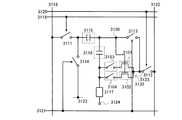
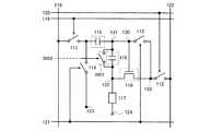
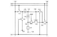
(実施の形態1)
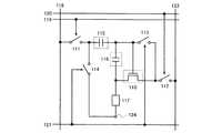
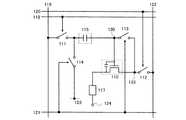
本発明の画素の基本構成について、図1を用いて説明する。図1に示す画素は、トラン
ジスタ110、第1のスイッチ111、第2のスイッチ112、第3のスイッチ113、
第4のスイッチ114、第1の容量素子115、第2の容量素子116、発光素子117
を有する。なお、画素は、信号線118、第1の走査線119、第2の走査線120、第
3の走査線121、電源線122及び電位供給線123に接続されている。本実施の形態
において、トランジスタ110はNチャネル型トランジスタとし、そのゲート・ソース間
電圧(Vgs)がしきい値電圧(Vth)を上回ったとき、導通状態になるものとする。
また、発光素子117の画素電極は陽極、対向電極124は陰極として機能する。なお、
トランジスタのゲート・ソース間電圧はVgs、ドレイン・ソース間電圧はVds、しき
い値電圧はVth、第1の容量素子115及び第2の容量素子116に蓄積された電圧は
それぞれVc1、Vc2と記し、電源線122、電位供給線123及び信号線118を、
それぞれ第1の配線、第2の配線、第3の配線とも呼ぶ。また、第1の走査線119、第
2の走査線120及び第3の走査線121を、それぞれ第4の配線、第5の配線、第6の
配線と呼んでも良い。Hereinafter, one aspect of the present invention will be described. However, it is easily understood by those skilled in the art that the present invention can be carried out in many different modes, and the forms and details thereof can be variously changed without departing from the spirit and scope of the present invention. Will be done. Therefore, the interpretation is not limited to the description content of this embodiment. In the configuration of the present invention described below, reference numerals indicating the same thing are commonly used among different drawings.
(Embodiment 1)
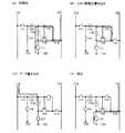
The basic configuration of the pixels of the present invention will be described with reference to FIG. The pixels shown in FIG. 1 include a
Have. The pixels are connected to the
Further, the pixel electrode of the
The gate-source voltage of the transistor is Vgs, the drain-source voltage is Vds, the threshold voltage is Vth, and the voltages stored in the first
They are also called the first wiring, the second wiring, and the third wiring, respectively. Further, the
トランジスタ110の第1の電極(ソース電極及びドレイン電極の一方)は、発光素子
117の画素電極に接続され、第2の電極(ソース電極及びドレイン電極の他方)は第2
のスイッチ112を介して電源線122に接続され、ゲート電極は第3のスイッチ113
及び第2のスイッチ112を介して電源線122と接続されている。なお、第3のスイッ
チ113は、トランジスタ110のゲート電極と第2のスイッチ112との間に接続され
ている。The first electrode (one of the source electrode and the drain electrode) of the
The gate electrode is connected to the
And is connected to the
また、トランジスタ110のゲート電極と第3のスイッチ113との接続箇所をノード
130とすると、ノード130は第1の容量素子115及び第1のスイッチ111を介し
て信号線118と接続されている。つまり、第1の容量素子115の第1の電極が第1の
スイッチ111を介して信号線118に、第2の電極がトランジスタ110のゲート電極
に接続されている。また、第1の容量素子115の第1の電極は第4のスイッチ114を
介して電位供給線123とも接続されている。ノード130は、さらに第2の容量素子1
16を介してトランジスタ110の第1の電極とも接続されている。つまり、第2の容量
素子116の第1の電極がトランジスタ110のゲート電極と、第2の電極がトランジス
タ110の第1の電極に接続されている。これら容量素子は、配線、半導体層や電極によ
って絶縁膜を挟むことで形成しても良いし、場合によっては図55に示すようにトランジ
スタ110のゲート容量を用いて第2の容量素子116を省略することも可能である。こ
れらの電圧を保持する手段を保持容量と言う。また、ノード130と、第1の容量素子1
15の第2の電極と第2の容量素子116の第1の電極とが接続されている配線との接続
箇所をノード131、トランジスタ110の第1の電極と、第2の容量素子116の第2
の電極と発光素子117の画素電極とが接続されている配線との接続箇所をノード132
、及びトランジスタ110の第2の電極と、第2のスイッチ112と第3のスイッチ11
3とが接続されている配線との接続箇所をノード133とする。Further, assuming that the connection point between the gate electrode of the
It is also connected to the first electrode of the
The connection points of the wiring to which the second electrode of 15 and the first electrode of the
, And the second electrode of the
The connection point with the wiring to which 3 is connected is referred to as
なお、第1の走査線119、第2の走査線120、第3の走査線121に信号を入力す
ることにより、それぞれ第1のスイッチ111、第2のスイッチ112、第3のスイッチ
113及び第4のスイッチ114のオンオフが制御される。By inputting signals to the
信号線118には、ビデオ信号に相当する画素の階調に従った信号、即ち輝度データに
応じた電位が入力される。A signal according to the gradation of pixels corresponding to a video signal, that is, a potential corresponding to luminance data is input to the
次に、図1で示した画素の動作について図2のタイミングチャート及び図3を用いて説
明する。なお、図2において1画面分の画像を表示する期間に相当する1フレーム期間は
、初期化期間、しきい値電圧書き込み期間、データ書き込み期間及び発光期間に分割され
る。また、初期化期間、しきい値電圧書き込み期間、データ書き込み期間をまとめてアド
レス期間と呼ぶ。1フレーム期間は特に限定はないが、画像をみる人がちらつき(フリッ
カ)を感じないように少なくとも1/60秒以下とすることが好ましい。Next, the operation of the pixels shown in FIG. 1 will be described with reference to the timing chart of FIG. 2 and FIG. The one-frame period corresponding to the period for displaying an image for one screen in FIG. 2 is divided into an initialization period, a threshold voltage writing period, a data writing period, and a light emitting period. Further, the initialization period, the threshold voltage writing period, and the data writing period are collectively referred to as an address period. The period of one frame is not particularly limited, but it is preferably at least 1/60 second or less so that the viewer does not feel flicker.
なお、発光素子117の対向電極124にはV1の電位(V1:任意の数)が入力され
る。また、発光素子117が発光するために少なくとも必要とする電位差をVELとする
と、電源線122にはV1+VEL+Vth+α(α:任意の正の数)の電位が入力され
る。つまり、電源線122はV1+VEL+Vth+α以上の電位であれば良い。電位供
給線123の電位は特に限定されないが、画素が形成されたパネルに入力する電位の範囲
内であることが好ましい。こうすることで、電源を別途作製する必要がなくなる。なお、
ここでは電位供給線123の電位をV2とする。The potential of V1 (V1: an arbitrary number) is input to the
Here, the potential of the
まず、図2(A)及び図3(A)に示すように初期化期間では、第1のスイッチ111
をオフとし、第2のスイッチ112、第3のスイッチ113及び第4のスイッチ114を
オンとする。このとき、トランジスタ110は導通状態であり、第1の容量素子115に
はV1+VEL+Vth+α−V2が、第2の容量素子116にはVth+αが保持され
る。なお、初期化期間では、第1の容量素子115には所定の電圧が、第2の容量素子1
16には少なくともVthより高い電圧が保持されれば良い。First, as shown in FIGS. 2A and 3A, in the initialization period, the
Is turned off, and the
16 may hold at least a voltage higher than Vth.
図2(B)及び図3(B)に示すしきい値電圧書き込み期間では、第2のスイッチ11
2をオフとする。そのため、トランジスタ110の第1の電極即ちソース電極の電位は次
第に上昇し、トランジスタ110のゲート・ソース間電圧Vgsがしきい値電圧(Vth
)となったところでトランジスタ110は非導通状態となる。よって、第2の容量素子1
16に保持される電圧Vc2はおおむねVthとなる。In the threshold voltage writing period shown in FIGS. 2 (B) and 3 (B), the
), The
The voltage Vc2 held at 16 is approximately Vth.
その後の図2(C)及び図3(C)に示すデータ書き込み期間においては、第3のスイ
ッチ113及び第4のスイッチ114をオフとした後、第1のスイッチ111をオンとし
、信号線118より輝度データに応じた電位(V2+Vdata)を入力する。このとき
に、第2の容量素子116に保持される電圧Vc2は、第1の容量素子115、第2の容
量素子116及び発光素子117の静電容量をそれぞれC1、C2、C3とするとC3>
>C1、C2より式(1)のように表すことができる。In the subsequent data writing period shown in FIGS. 2 (C) and 3 (C), the
> C1 and C2 can be expressed as equation (1).

なお、C1とC2は信号線118より供給する電位を決定する際に必要であるが、これ
らの関係は特に限定されない。なお、C1>C2の場合には、輝度変化に伴うVdata
の振幅を少なくすることが可能であるため消費電力を低減することができる。一方、C2
>C1の場合には、周囲のスイッチのオン、オフやオフ電流によるVc2の変化を抑制す
ることができる。これらの相反する効果よりC1とC2は等しく、第1の容量素子115
と第2の容量素子116の大きさは同じであることが好ましい。Note that C1 and C2 are necessary for determining the potential supplied from the
Since it is possible to reduce the amplitude of the power consumption, the power consumption can be reduced. On the other hand, C2
In the case of> C1, the change of Vc2 due to the on / off or off current of the surrounding switches can be suppressed. Due to these contradictory effects, C1 and C2 are equal, and the first
And the size of the
なお、次の発光期間において発光素子117を非発光としたい場合には、Vdata≦
0の電位を入力すれば良い。If it is desired to make the
The potential of 0 may be input.
次に、図2(D)及び図3(D)に示す発光期間では、第1のスイッチ111をオフと
した後、第2のスイッチ112をオンとする。このとき、トランジスタ110のゲート・
ソース間電圧はVgs=Vth+Vdata×(C1/(C1+C2))であり、輝度デ
ータに応じた電流がトランジスタ110及び発光素子117に流れ、発光素子117が発
光する。もちろん、信号線118より入力される輝度データに応じた電位は、トランジス
タ110のゲート・ソース間電圧がVgs=Vth+Vdata×(C1/(C1+C2
))となることを考慮してVdataを決定する。Next, in the light emitting period shown in FIGS. 2 (D) and 3 (D), the
The voltage between sources is Vgs = Vth + Vdata × (C1 / (C1 + C2)), a current corresponding to the luminance data flows through the
)) Is taken into consideration when determining Vdata.
なお、発光素子117に流れる電流Iは、トランジスタ110を飽和領域で動作させた
場合、式(2)で表される。The current I flowing through the
また、トランジスタ110を線形領域で動作させた場合、発光素子117に流れる電流
Iは式(3)で表される。Further, when the
ここで、Wはトランジスタ110のチャネル幅、Lはチャネル長、μは移動度、Cox
は蓄積容量を指す。Here, W is the channel width of the
Refers to the storage capacity.
式(2)及び式(3)より、トランジスタ110の動作領域が飽和領域、線形領域のい
ずれの場合においても、発光素子117に流れる電流は、トランジスタ110のしきい値
電圧(Vth)に依存しない。よって、トランジスタ110のしきい値電圧のばらつきに
起因した電流値のばらつきを抑制し、輝度データに対応した電流を発光素子117に供給
することができる。From equations (2) and (3), the current flowing through the
以上のことから、トランジスタ110のしきい値電圧のばらつきに起因した輝度のばら
つきを抑制することができる。また、対向電極の電位を一定として動作させるため消費電
力を低くすることが可能となる。From the above, it is possible to suppress the variation in brightness caused by the variation in the threshold voltage of the
さらに、トランジスタ110を飽和領域で動作させた場合においては、発光素子117
の劣化による輝度のばらつきも抑制できる。なお、発光素子の劣化は、その電流電圧特性
が劣化前に比べ平行にシフトした場合に限られない。例えば、特性の傾きや特性が曲線で
表される際にはその微分値が劣化前と比べ異なる場合も含まれる。発光素子117が劣化
すると、発光素子117のVELは増大し、トランジスタ110の第1の電極、即ちソー
ス電極の電位は上昇する。このとき、トランジスタ110のソース電極は第2の容量素子
116の第2の電極に、トランジスタ110のゲート電極は第2の容量素子116の第1
の電極に接続されており、なおかつゲート電極側は浮遊状態となっている。そのため、ソ
ース電位の上昇に伴い、同じ電位だけトランジスタ110のゲート電位も上昇する。よっ
て、トランジスタ110のVgsは変化しないため、たとえ発光素子が劣化してもトラン
ジスタ110及び発光素子117に流れる電流に影響しない。なお、式(2)においても
発光素子に流れる電流Iはソース電位やドレイン電位に依存しないことがわかる。Further, when the
It is also possible to suppress variations in brightness due to deterioration of. The deterioration of the light emitting element is not limited to the case where the current-voltage characteristic is shifted in parallel as compared with that before the deterioration. For example, when the slope or characteristic of a characteristic is represented by a curve, the differential value may be different from that before deterioration. When the
It is connected to the electrode of, and the gate electrode side is in a floating state. Therefore, as the source potential rises, the gate potential of the
よって、トランジスタ110を飽和領域で動作させた場合においては、トランジスタ1
10のしきい値電圧のばらつき及び発光素子117の劣化に起因したトランジスタ110
に流れる電流のばらつきを抑制することができる。Therefore, when the
It is possible to suppress the variation of the current flowing through.
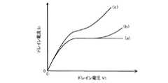
なお、トランジスタ110を飽和領域で動作させた場合、チャネル長Lが短いほど、降
伏現象によりドレイン電圧を著しく増大させると電流が大量に流れやすい。When the
また、ドレイン電圧をピンチオフ電圧より増大させるとピンチオフ点がソース側に移動
し、実質チャネルとして機能する実効的なチャネル長は減少する。これにより、電流値が
増大する。この現象をチャネル長変調と呼ぶ。なお、ピンチオフ点とはチャネルが消滅し
ていきゲート下においてチャネルの厚さが0となる境界箇所であり、ピンチオフ電圧とは
ピンチオフ点がドレイン端となる時の電圧を指す。この現象も、チャネル長Lが短いほど
起こり易い。例えば、チャネル長変調による電圧−電流特性のモデル図を図4に示す。な
お、図4において、トランジスタのチャネル長Lは(a)>(b)>(c)である。Further, when the drain voltage is increased above the pinch-off voltage, the pinch-off point moves to the source side, and the effective channel length functioning as a substantial channel decreases. This increases the current value. This phenomenon is called channel length modulation. The pinch-off point is a boundary point where the channel disappears and the thickness of the channel becomes 0 under the gate, and the pinch-off voltage refers to the voltage when the pinch-off point becomes the drain end. This phenomenon is also more likely to occur as the channel length L is shorter. For example, a model diagram of the voltage-current characteristic by channel length modulation is shown in FIG. In FIG. 4, the channel length L of the transistor is (a)>(b)> (c).
以上のことから、トランジスタ110を飽和領域で動作させる場合、ドレイン・ソース
間電圧Vdsに対する電流Iはより一定に近い方が好ましい。よって、トランジスタ11
0のチャネル長Lは長い方がより好ましい。たとえば、トランジスタのチャネル長Lはチ
ャネル幅Wより大きい方が好ましい。また、チャネル長Lは10μm以上50μm以下、
より望ましくは15μm以上40μm以下が好ましい。ただし、チャネル長L及びチャネ
ル幅Wはこれに限定されない。From the above, when the
It is more preferable that the channel length L of 0 is long. For example, the channel length L of the transistor is preferably larger than the channel width W. The channel length L is 10 μm or more and 50 μm or less.
More preferably, it is 15 μm or more and 40 μm or less. However, the channel length L and the channel width W are not limited to this.
以上のようにトランジスタのしきい値電圧のばらつきに起因した電流値のばらつきを抑
制することができるため、本発明においてそのトランジスタによって制御された電流の供
給先は特に限定されない。そのため、図1に示した発光素子117は、代表的にはEL素
子(有機EL素子、無機EL素子又は有機物及び無機物を含むEL素子)を適用すること
ができる。また、発光素子117に換えて、電子放出素子、液晶素子、電子インクなどを
適用することもできる。図5に発光素子117にEL素子517を用いた例を示す。なお
、図5は画素電極511から対向電極124に電流が流れている様子を示している。As described above, since the variation in the current value due to the variation in the threshold voltage of the transistor can be suppressed, the supply destination of the current controlled by the transistor is not particularly limited in the present invention. Therefore, as the
また、トランジスタ110は発光素子117に供給する電流を制御する機能を有してい
れば良いため、特にトランジスタの種類は限定されず様々なものを用いることができる。
例えば、結晶性半導体膜を用いた薄膜トランジスタ(TFT)、非晶質シリコンや多結晶
シリコンに代表される非単結晶半導体膜を用いた薄膜トランジスタ、半導体基板やSOI
基板を用いて形成されるトランジスタ、MOS型トランジスタ、接合型トランジスタ、バ
イポーラトランジスタ、ZnOやa−InGaZnOなどの化合物半導体を用いたトラン
ジスタ、有機半導体やカーボンナノチューブを用いたトランジスタ、その他のトランジス
タをトランジスタ110に適用することができる。Further, since the
For example, a thin film transistor (TFT) using a crystalline semiconductor film, a thin film transistor using a non-single crystal semiconductor film typified by amorphous silicon or polycrystalline silicon, a semiconductor substrate or SOI.
Transistors formed using a substrate, MOS type transistors, junction type transistors, bipolar transistors, transistors using compound semiconductors such as ZnO and a-InGaZnO, transistors using organic semiconductors and carbon nanotubes, and other transistors are used as
第1のスイッチ111は輝度データに応じた電位、即ちビデオ信号を信号線118より
画素に入力するタイミングを選択し、主に第1の容量素子115に保持される電圧、及び
第2の容量素子116に保持される電圧即ちトランジスタ110のゲート・ソース間電圧
を変化させるものである。また、第2のスイッチ112はトランジスタ110の第2の電
極に所定の電位を供給するタイミングを選択するものである。なお、場合によっては第1
の容量素子115の第2の電極及び第2の容量素子116の第1の電極にも前記所定の電
位を供給する。第3のスイッチ113は、トランジスタ110のゲート電極と第2の電極
との接続を制御するものであり、第4のスイッチ114は各フレーム期間毎に第1の容量
素子115に所定の電圧を保持させるタイミングを選択し、第1の容量素子115の第1
の電極に所定の電位を供給するか否かを制御するものである。そのため、第1のスイッチ
111、第2のスイッチ112、第3のスイッチ113、第4のスイッチ114は、上記
機能を有していれば特に限定されない。たとえば、トランジスタやダイオードでもよいし
、それらを組み合わせた論理回路でもよい。なお、第1のスイッチ111、第2のスイッ
チ112及び第4のスイッチ114は、上記タイミングで信号もしくは電位を画素に与え
ることができれば特に必要はない。また、第3のスイッチ113においても上記機能を実
現できれば特に必要はない。The
The predetermined potential is also supplied to the second electrode of the
It controls whether or not a predetermined potential is supplied to the electrodes of. Therefore, the
例えば、初期化期間及びしきい値電圧書き込み期間において第1の容量素子115に所
定の電圧を保持させることができ、さらに画素の階調に従った信号をデータ書き込み期間
に画素に入力することができる場合には、画素内に第1のスイッチ111及び第4のスイ
ッチ114を設けなくても良い。さらに、画素に初期期間及び発光期間においてV1+V
EL+Vth+α(α>0)を供給することが可能であれば図43に示すように第2のス
イッチ112を特に設けなくても良い。図43に示す画素は、トランジスタ110、第1
の容量素子115、第3のスイッチ113、画素電極4300を有する。そして、トラン
ジスタ110の第1の電極(ソース電極及びドレイン電極の一方)は画素電極4300に
接続され、ゲート電極は第3のスイッチ113を介してトランジスタ110の第2の電極
と接続されている。また、トランジスタ110のゲート電極は第1の容量素子115の第
2の電極とも接続されている。なお、第1の容量素子115の第1の電極には階調に従っ
た信号、即ち輝度データに応じた電位(即ち、V2+Vdata)及び第1の容量素子1
15に所定の電圧を保持させるための任意の電位(即ち、V2)が所定の期間に供給され
る。なお、トランジスタ110のゲート容量4310を保持容量として利用しているため
、図1における第2の容量素子116を特に設ける必要なない。このような画素において
も、図2に示すタイミングチャートと同様にそれぞれの電極に所望の電位を供給すること
で、トランジスタ110のしきい値電圧のばらつきに起因した電流値のばらつきを抑制す
ることができる。よって、画素電極4300に所望の電流を供給することができる。もち
ろん、図1における第2の容量素子116においてもトランジスタ110のゲート容量を
利用し、省略することも可能である。For example, the first
If it is possible to supply EL + Vth + α (α> 0), the
It has a
An arbitrary potential (ie, V2) for causing 15 to hold a predetermined voltage is supplied in a predetermined period. Since the
次に、図6に第1のスイッチ111、第2のスイッチ112、第3のスイッチ113及
び第4のスイッチ114にNチャネル型のトランジスタを適用した場合について示す。な
お、図1の構成と共通するところは、共通の符号を用いてその説明を省略する。Next, FIG. 6 shows a case where an N-channel transistor is applied to the
第1のスイッチングトランジスタ611が図1における第1のスイッチ111に相当し
、第2のスイッチングトランジスタ612が第2のスイッチ112に相当し、第3のスイ
ッチングトランジスタ613が第3のスイッチ113に相当し、第4のスイッチングトラ
ンジスタ614が第4のスイッチ114に相当する。なお、トランジスタ110のチャネ
ル長は、第1のスイッチングトランジスタ611、第2のスイッチングトランジスタ61
2、第3のスイッチングトランジスタ613及び第4のスイッチングトランジスタ614
のいずれのトランジスタのチャネル長より長い方が好ましい。The
2.
It is preferable that the length is longer than the channel length of any of the transistors.
第1のスイッチングトランジスタ611はゲート電極が第1の走査線119に、第1の
電極が信号線118に、第2の電極が第1の容量素子115の第1の電極に接続されてい
る。In the
また、第2のスイッチングトランジスタ612はゲート電極が第2の走査線120に接
続され、第1の電極がノード133に接続され、第2の電極が電源線122に接続されて
いる。Further, in the
第3のスイッチングトランジスタ613はゲート電極が第3の走査線121に接続され
、第1の電極がノード130に接続され、第2の電極がノード133に接続されている。In the
また、第4のスイッチングトランジスタ614はゲート電極が第3の走査線121に接
続され、第1の電極が第1の容量素子115の第1の電極に接続され、第2の電極が電位
供給線123に接続されている。Further, in the
各々のスイッチングトランジスタは、それぞれの走査線に入力される信号がHレベルの
ときにオンとなり、入力される信号がLレベルのときにオフとなる。Each switching transistor is turned on when the signal input to each scanning line is H level, and turned off when the input signal is L level.
図6に示した画素のレイアウトの一形態を上面図を用いて図44に示す。なお、トラン
ジスタや容量素子、発光素子等の構成については後述の実施形態で説明するため、ここで
はレイアウトについてのみ説明する。また、図44に示すトランジスタ110及び第1の
スイッチングトランジスタ611乃至第4のスイッチングトランジスタ614には、半導
体層の下にゲート電極が位置するボトムゲート型のトランジスタを用いている。One form of the pixel layout shown in FIG. 6 is shown in FIG. 44 with a top view. Since the configurations of the transistor, the capacitive element, the light emitting element, and the like will be described in the embodiments described later, only the layout will be described here. Further, as the
図44に示す導電層4410は、第1の走査線119と第1のスイッチングトランジス
タ611のゲート電極として機能する部分を含み、導電層4411は信号線118と第1
のスイッチングトランジスタ611の第1の電極として機能する部分を含む。また、導電
層4412は、第1のスイッチングトランジスタ611の第2の電極と、第1の容量素子
115の第1の電極と、第4のスイッチングトランジスタ614の第1の電極として機能
する部分を含む。導電層4413は、第1の容量素子115の第2の電極と、第2の容量
素子116の第1の電極と、トランジスタ110のゲート電極として機能する部分を含む
。なお、この導電層4413は、配線4414を介して第3のスイッチングトランジスタ
613の第1の電極として機能する部分を含む導電層4415と接続されている。導電層
4416は、第2の容量素子116の第2の電極と、トランジスタ110の第1の電極と
して機能する部分を含み、コンタクトを介して発光素子の画素電極4455と接続されて
いる。また、導電層4417は、トランジスタ110の第2の電極と、第3のスイッチン
グトランジスタ613の第2の電極と、第2のスイッチングトランジスタ612の第1の
電極として機能する部分を含み、導電層4418は、電源線122と、第2のスイッチン
グトランジスタ612の第2の電極として機能する部分を含む。導電層4419は、第2
の走査線120と、第2のスイッチングトランジスタ612のゲート電極として機能する
部分を含む。導電層4420は、第3のスイッチングトランジスタ613のゲート電極と
、第4のスイッチングトランジスタ614のゲート電極として機能する部分を含み、配線
4421を介して第3の走査線121と接続されている。また、第4のスイッチングトラ
ンジスタ614の第2の電極として機能する部分を含む導電層4422は、配線4423
を介して電位供給線123と接続されている。The
Includes a portion that functions as the first electrode of the switching
The
It is connected to the
なお、各々の導電層のうち第1のスイッチングトランジスタ611のゲート電極、第1
の電極及び第2の電極として機能する部分は、それぞれを含む導電層と半導体層4431
とが重なって形成されている部分であり、第2のスイッチングトランジスタ612のゲー
ト電極、第1の電極及び第2の電極として機能する部分は、それぞれを含む導電層と半導
体層4432とが重なって形成されている部分である。また、各々の導電層のうち第3の
スイッチングトランジスタ613のゲート電極、第1の電極及び第2の電極として機能す
る部分は、それぞれを含む導電層と半導体層4433と重なって形成されている部分であ
り、第4のスイッチングトランジスタ614のゲート電極、第1の電極及び第2の電極と
して機能する部分は、それぞれを含む導電層と半導体層4434とが重なって形成されて
いる部分である。同様に、トランジスタ110においても、ゲート電極、第1の電極及び
第2の電極として機能する部分は、それぞれを含む導電層と半導体層4430と重なって
形成されている導電層部分である。なお、第1の容量素子115は、導電層4412と導
電層4413とが重なっている部分に、第2の容量素子116は導電層4413と導電層
4416とが重なっている部分に形成されている。Of the respective conductive layers, the gate electrode of the
The electrode and the part that functions as the second electrode are the conductive layer and the
In the portion formed by overlapping the two, and the portion that functions as the gate electrode, the first electrode, and the second electrode of the
なお、導電層4410、導電層4413、導電層4419、導電層4420、第3の走
査線121及び電位供給線123は、同一材料で同じ層を用いて作製することができる。
半導体層4430、半導体層4431、半導体層4432、半導体層4433及び半導体
層4434や、導電層4411、導電層4412、導電層4415、導電層4416、導
電層4417、導電層4418及び導電層4422は、それぞれ同一材料で同じ層を用い
て作製することができる。また、画素電極4455と同一材料で同じ層を用いて、配線4
414、配線4421、配線4423を作製することができる。The
The
414,
図44に示すように、第1のスイッチングトランジスタ611を除く各々のトランジス
タにおいてソース電極及びドレイン電極の一方が他方の電極を包み囲むような構造とする
ことで、チャネル幅をかせぐことができる。よって、画素を構成するトランジスタの半導
体層に結晶性半導体層より移動度の低い非晶質半導体層を用いた際には特に有効である。
もちろん、第1のスイッチングトランジスタ611においても、ソース電極及びドレイン
電極の一方が他方の電極を包み囲むような構造としても良い。As shown in FIG. 44, the channel width can be increased by forming a structure in which one of the source electrode and the drain electrode surrounds the other electrode in each transistor except the
Of course, the
次に、図6に示した画素の図44とは異なるレイアウトの一形態を上面図を用いて図4
5に示す。なお、図45に示すトランジスタ110及び第1のスイッチングトランジスタ
611乃至第4のスイッチングトランジスタ614には、半導体層上にゲート電極が位置
する順スタガ型等のトップゲート型トランジスタを用いている。Next, using a top view, a form of layout of the pixels shown in FIG. 6, which is different from that of FIG.
Shown in 5. For the
図45において、導電層4510は、第1の走査線119と第1のスイッチングトラン
ジスタ611のゲート電極として機能する部分を含み、導電層4511は信号線118と
第1のスイッチングトランジスタ611の第1の電極として機能する部分を含む。半導体
膜4520は、第1のスイッチングトランジスタ611の半導体層及び第2の電極として
機能する部分、第4のスイッチングトランジスタ614の第1の電極及び半導体層として
機能する部分、第1の容量素子115の第1の電極として機能する部分を含む。なお、半
導体膜4520は配線4512を介して電位供給線123と接続されており、配線451
2は第4のスイッチングトランジスタ614の第2の電極として機能する。また、導電層
4513は、第1の容量素子115の第2の電極と、第2の容量素子116の第1の電極
とトランジスタ110のゲート電極として機能する部分を含む。なお、導電層4513は
第3のスイッチングトランジスタ613の第1の電極として機能する配線4514を介し
て半導体膜4521と接続されている。この半導体膜4521は、第3のスイッチングト
ランジスタ613の半導体層及び第2の電極として機能する部分、第2のスイッチングト
ランジスタ612の第1の電極及び半導体層として機能する部分、トランジスタ110の
第1の電極、半導体及び第2の電極として機能する部分、さらには第2の容量素子116
の第2の電極として機能する部分を含む。導電層4515は、第2の走査線120と、第
2のスイッチングトランジスタ612のゲート電極として機能する部分を含む。導電層4
516は、電源線122と、第2のスイッチングトランジスタ612の第2の電極として
機能する部分を含む。導電層4517は、第3のスイッチングトランジスタ613のゲー
ト電極として機能する部分、及び第4のスイッチングトランジスタ614のゲート電極と
して機能する部分を含み、配線4518を介して第3の走査線121と接続されている。
なお、発光素子の画素電極4545は配線4519を介して半導体膜4521と接続され
ている。In FIG. 45, the
Includes a portion that functions as a second electrode of. The
Reference numeral 516 includes a
The
なお、第1の容量素子115は、半導体膜4520と導電層4513とが重なっている
部分に、第2の容量素子116は半導体膜4521と導電層4513とが重なっている部
分に形成されている。The first
また、導電層4510、導電層4513、導電層4515、導電層4517、第3の走
査線121及び電位供給線123は、同一材料で同じ層を用いて作製することができる。
半導体膜4520、半導体膜4521も同一材料で同じ層を用いて作製することができる
。また、導電層4511と同一材料で同じ層を用いて、配線4512、配線4514、導
電層4516、配線4518を作製することができる。Further, the
The
なお、画素のレイアウトは上記に限定されるものではない。 The pixel layout is not limited to the above.
図6の画素構成においても、図1と同様の動作方法によりトランジスタ110のしきい
値電圧のばらつきに起因した電流値のばらつきを抑制することができる。よって、輝度デ
ータに対応した電流を発光素子117に供給することができ、輝度のばらつきを抑制する
ことが可能となる。また、トランジスタ110を飽和領域で動作させた場合においては、
発光素子117の劣化に起因した輝度のばらつきも抑制することができる。Also in the pixel configuration of FIG. 6, the variation in the current value due to the variation in the threshold voltage of the
Variations in brightness due to deterioration of the
また、Nチャネル型のトランジスタのみで画素を構成することができるため、製造工程
の簡略化を図ることができる。また、画素を構成するトランジスタの半導体層に非晶質半
導体、セミアモルファス半導体などを用いることができる。例えば、非晶質半導体として
アモルファスシリコン(a−Si:H)が挙げられる。これらの半導体を用いることによ
り、さらに製造工程の簡略化が可能である。したがって、製造コストの削減や歩留まりの
向上を図ることができる。Further, since the pixel can be formed only by the N-channel type transistor, the manufacturing process can be simplified. Further, an amorphous semiconductor, a semi-amorphous semiconductor, or the like can be used for the semiconductor layer of the transistor constituting the pixel. For example, amorphous silicon (a-Si: H) can be mentioned as an amorphous semiconductor. By using these semiconductors, the manufacturing process can be further simplified. Therefore, it is possible to reduce the manufacturing cost and improve the yield.
なお、第1のスイッチングトランジスタ611、第2のスイッチングトランジスタ61
2、第3のスイッチングトランジスタ613及び第4のスイッチングトランジスタ614
は、単なるスイッチとして動作させるため、トランジスタの極性(導電型)は特に限定さ
れない。ただし、オフ電流が少ないトランジスタを用いることが望ましい。オフ電流が少
ないトランジスタとしては、LDD領域を設けているものやマルチゲート構造にしている
ものなどがある。また、Nチャネル型とPチャネル型の両方を用いて、CMOS型のスイ
ッチにしてもよい。The
2.
Is operated as a mere switch, so that the polarity of the transistor (conductive type) is not particularly limited. However, it is desirable to use a transistor with a small off current. Transistors with a small off-current include those provided with an LDD region and those having a multi-gate structure. Further, both the N-channel type and the P-channel type may be used to make a CMOS type switch.
また、図1と同様の動作を行うものであれば、スイッチの接続は様々な構成をとること
ができ、図1に限定されない。図1の画素構成の動作を説明した図3からわかるように、
本発明では初期化期間、しきい値電圧書き込み期間、データ書き込み期間及び発光期間は
、それぞれ図53(A)乃至(D)に示す実線のように導通がとれていれば良い。よって
、これを満たすようにスイッチ等を配置し動作させうる構成であれば良い。Further, as long as the operation is the same as that shown in FIG. 1, the switch connection can have various configurations and is not limited to FIG. As can be seen from FIG. 3, which explains the operation of the pixel configuration of FIG.
In the present invention, the initialization period, the threshold voltage writing period, the data writing period, and the light emitting period may be conducted as shown by the solid lines shown in FIGS. 53 (A) to 53 (D), respectively. Therefore, any configuration may be used as long as the switch or the like can be arranged and operated so as to satisfy this.
また、初期化期間では、第1の容量素子115に所定の電圧が、第2の容量素子116
には少なくともトランジスタ110のしきい値電圧Vthより高い電圧が保持されれば良
いため、図54に示すようにノード132は第5のスイッチ5405を介して電位供給線
5401と接続されていても良い。この第5のスイッチ5405は初期化期間のみオンす
るものとし、図54では第5のスイッチ5405のオン、オフを制御する走査線は図示し
ていない。なお、電位供給線5401の電位は、V1+VELより低い電位であれば良い
。より好ましくは、V1以下の電位であり、このような電位とすることで発光素子117
に逆方向のバイアス電圧が印加できるため、発光素子における短絡箇所を絶縁化したり、
発光素子の劣化を抑制することができる。よって、発光素子の寿命を延ばすことができる
。Further, in the initialization period, a predetermined voltage is applied to the
As long as a voltage higher than the threshold voltage Vth of the
Since a bias voltage in the opposite direction can be applied to the light emitting element, the short-circuited part in the light emitting element can be insulated.
Deterioration of the light emitting element can be suppressed. Therefore, the life of the light emitting element can be extended.
続いて、上述した本発明の画素を有する表示装置について図7を用いて説明する。 Subsequently, the display device having the pixels of the present invention described above will be described with reference to FIG. 7.
表示装置は、信号線駆動回路711、走査線駆動回路712及び画素部713を有し、
画素部713は、信号線駆動回路711から列方向に伸張して配置された複数の信号線S
1〜Sm及び電源線P1_1〜Pm_1、走査線駆動回路712から行方向に伸張して配
置された複数の第1の走査線G1_1〜Gn_1、第2の走査線G1_2〜Gn_2、第
3の走査線G1_3〜Gn_3及び電位供給線P1_2〜Pn_2、並びに信号線S1〜
Smに対応してマトリクス状に配置された複数の画素714を有する。そして、各画素7
14は、信号線Sj(信号線S1〜Smのうちいずれか一)、電源線Pj_1、第1の走
査線Gi_1(走査線G1_1〜Gn_1のうちいずれか一)、第2の走査線Gi_2、
第3の走査線Gi_3及び電位供給線Pi_2と接続されている。The display device includes a signal
The
1-Sm and power supply lines P1-1 to Pm_1, a plurality of first scanning lines G1-1 to Gn_1 extending in the row direction from the scanning
It has a plurality of
It is connected to the third scanning line Gi_3 and the potential supply line Pi_2.
なお、信号線Sj、電源線Pj_1、第1の走査線Gi_1、第2の走査線Gi_2、
第3の走査線Gi_3、電位供給線Pi_2は、それぞれ図1の信号線118、電源線1
22、第1の走査線119、第2の走査線120、第3の走査線121、電位供給線12
3に相当する。The signal line Sj, the power supply line Pj_1, the first scanning line Gi_1, the second scanning line Gi_2,
The third scanning line Gi_3 and the potential supply line Pi_2 are the
22,
Corresponds to 3.
走査線駆動回路712から出力される信号により、動作させる画素の行を選択すると共
に同行に属するそれぞれの画素に対し同時に図2に示した動作を行う。なお、図2のデー
タ書き込み期間においては、選択された行の画素に信号線駆動回路711から出力された
ビデオ信号を書き込む。このとき、それぞれの画素の輝度データに応じた電位が各信号線
S1〜Smに入力される。The row of pixels to be operated is selected by the signal output from the scanning
図8に示すように、例えばi行目のデータ書き込み期間を終えるとi+1行目に属する
画素へ信号の書き込みを行う。なお、図8には、各行におけるデータ書き込み期間を表す
ためにこれを忠実に表すことができる図2の第1のスイッチ111の動作を抜粋し記載し
ている。そして、i行目においてデータ書き込み期間を終えた画素は、発光期間に移り、
その画素へ書き込まれた信号にしたがって発光する。As shown in FIG. 8, for example, when the data writing period of the i-th row is completed, the signal is written to the pixels belonging to the i + 1th line. Note that FIG. 8 shows an excerpt of the operation of the
It emits light according to the signal written to the pixel.
よって、各行におけるデータ書き込み期間さえ重複しなければ、各行自由に初期化開始
時期を設定することができる。また、各画素は自身のアドレス期間を除き発光することが
可能であるため、1フレーム期間における発光期間の割合(即ち、デューティー比)を非
常に大きくでき、おおむね100%にすることも可能となる。よって、輝度のばらつきが
少なくデューティー比が高い表示装置を得ることができる。Therefore, as long as the data writing period in each line does not overlap, the initialization start time can be freely set in each line. Further, since each pixel can emit light except for its own address period, the ratio of the light emitting period in one frame period (that is, the duty ratio) can be made very large, and it is also possible to make it approximately 100%. .. Therefore, it is possible to obtain a display device having a high duty ratio with little variation in brightness.
また、しきい値電圧書き込み期間を長く設定することも可能であるため、トランジスタ
のしきい値電圧をより正確に容量素子に書き込むことができる。よって、表示装置として
の信頼性を向上させることができる。Further, since the threshold voltage writing period can be set to be long, the threshold voltage of the transistor can be written to the capacitive element more accurately. Therefore, the reliability of the display device can be improved.
なお、図7に示した表示装置の構成は一例であって本発明はこれに限定されない。例え
ば、電位供給線P1_2〜Pn_2は第1の走査線G1_1〜Gn_1と平行に配置され
ている必要はなく、信号線S1〜Smと平行に配置されていても良い。また、電源線P1
_1〜Pm_1においても信号線S1〜Smと平行に配置されている必要はなく、第1の
走査線G1_1〜Gn_1と平行に配置されていても良い。The configuration of the display device shown in FIG. 7 is an example, and the present invention is not limited thereto. For example, the potential supply lines P1_2 to Pn_2 need not be arranged in parallel with the first scanning lines G1_1 to Gn_1, and may be arranged in parallel with the signal lines S1 to Sm. Also, the power supply line P1
The _1 to Pm_1 need not be arranged in parallel with the signal lines S1 to Sm, and may be arranged in parallel with the first scanning lines G1_1 to Gn_1.
本実施形態では第3のスイッチ113及び第4のスイッチ114のオンオフは同一の走
査線、即ち第3の走査線121を用いて制御している場合について示したが、それぞれ異
なる走査線を用いて図2のタイミングチャートに従って各々のスイッチを制御しても良い
。In the present embodiment, the on / off of the
なお、しきい値電圧のばらつきには、画素間における各トランジスタのしきい値電圧の
違いのほか、1つのトランジスタに注目した場合において経時的なしきい値電圧の変化も
含むものとする。さらに、各トランジスタのしきい値電圧の違いは、トランジスタの作製
時におけるトランジスタ特性の違いによるものも含まれるものとする。なお、ここでいう
トランジスタは発光素子等の負荷に電流を供給する機能を有するトランジスタを指す。
(実施の形態2)
本実施形態では、実施の形態1とは異なる構成の画素を図9に示す。なお、実施の形態
1と同様のものに関しては共通の符号を用いて示し、同一部分又は同様な機能を有する部
分の詳細な説明は省略する。It should be noted that the variation in the threshold voltage includes not only the difference in the threshold voltage of each transistor between pixels but also the change in the threshold voltage over time when focusing on one transistor. Further, it is assumed that the difference in the threshold voltage of each transistor is due to the difference in the transistor characteristics at the time of manufacturing the transistor. The transistor referred to here refers to a transistor having a function of supplying a current to a load such as a light emitting element.
(Embodiment 2)
In the present embodiment, a pixel having a configuration different from that of the first embodiment is shown in FIG. The same parts as those in the first embodiment are shown by using common reference numerals, and detailed description of the same parts or parts having the same functions will be omitted.
図9(A)に示す画素は、トランジスタ110、第1のスイッチ111、第2のスイッ
チ112、第3のスイッチ113、整流素子914、第1の容量素子115、第2の容量
素子116、発光素子117を有する。なお、画素は、信号線118、第1の走査線11
9、第2の走査線120、第3の走査線921、第4の走査線922及び電源線122に
接続されている。図9(A)に示した画素は、図1における第4のスイッチ114に整流
素子914を用いた構成となっており、第1の容量素子115の第1の電極は、整流素子
914を介して第4の走査線922と接続されている。つまり、整流素子914は第1の
容量素子115の第1の電極から第4の走査線922に電流が流れるように接続されてい
る。もちろん、実施の形態1に示したように第1のスイッチ111、第2のスイッチ11
2及び第4のスイッチ114は、トランジスタ等を用いてもよい。また、整流素子914
には、図9(B)に示すショットキー・バリア型951、PIN型952、PN型953
などのダイオードの他、ダイオード接続されているトランジスタ954、955等を用い
ることができる。ただし、トランジスタ954及びトランジスタ955は、電流を流す方
向によってトランジスタの極性を適宜選択する必要がある。The pixels shown in FIG. 9A are a
9. It is connected to the
Transistors and the like may be used for the second and
The
In addition to the diode of However, in the
整流素子914は、第4の走査線922にHレベルの信号が入力されたときには電流が
流れず、Lレベルの信号が入力されたときには整流素子914に電流が流れる。よって、
図9の画素を図1に示した画素と同様に動作させる際には、初期化期間及びしきい値電圧
書き込み期間において第4の走査線922にLレベルの信号を入力し、それ以外の期間に
おいてはHレベルの信号を入力する。Lレベルの信号は整流素子914にただ電流が流れ
るだけではなく、実施の形態1と同様、画素に入力する輝度データに応じた電位を(V2
+Vdata)とすると第2の容量素子116の第1の電極の電位をV2にまで下げる必
要があるため、V2から整流素子914の順方向におけるしきい値電圧を引いた電位であ
ることとする。ただし、V2は任意の値であり、発光期間において発光素子117を非発
光としたい場合にはVdata=0の電位を入力すれば良い。また、Hレベルの信号は、
上述したように整流素子914に電流が流れなければ良いため、V2から整流素子914
の順方向におけるしきい値電圧を減算した値より大きければ良い。In the
When the pixels of FIG. 9 are operated in the same manner as the pixels shown in FIG. 1, an L level signal is input to the fourth scanning line 922 during the initialization period and the threshold voltage writing period, and other periods. In, an H level signal is input. The L-level signal not only causes a current to flow through the rectifying
Since + Vdata), it is necessary to lower the potential of the first electrode of the
As described above, it is sufficient that no current flows through the rectifying
It suffices if it is larger than the value obtained by subtracting the threshold voltage in the forward direction of.
上記事項を考慮し、図9の画素構成においても図1と同様に動作させることによりトラ
ンジスタ110のしきい値電圧のばらつきに起因した電流値のばらつきを抑制することが
できる。よって、輝度データに対応した電流を発光素子117に供給することができ、輝
度のばらつきを抑制することが可能となる。また、トランジスタ110を飽和領域で動作
させた場合においては、発光素子117の劣化に起因した輝度のばらつきも抑制すること
ができる。In consideration of the above items, the pixel configuration of FIG. 9 can be operated in the same manner as in FIG. 1 to suppress the variation in the current value due to the variation in the threshold voltage of the
また、本実施形態に示した画素を図7の表示装置に適用することができる。実施の形態
1と同様、各行におけるデータ書き込み期間さえ重複しなければ、各行自由に初期化開始
時期を設定することができる。また、各画素は自身のアドレス期間を除き発光することが
可能であるため、1フレーム期間における発光期間の割合(即ち、デューティー比)を非
常に大きくでき、おおむね100%にすることもできる。よって、輝度のばらつきが少な
くデューティー比が高い表示装置を得ることができる。Further, the pixels shown in the present embodiment can be applied to the display device of FIG. As in the first embodiment, the initialization start time can be freely set for each row as long as the data writing periods for each row do not overlap. Further, since each pixel can emit light except for its own address period, the ratio of the light emitting period in one frame period (that is, the duty ratio) can be made very large, and can be made approximately 100%. Therefore, it is possible to obtain a display device having a high duty ratio with little variation in brightness.
また、しきい値電圧書き込み期間を長く設定することも可能であるため、発光素子に流
れる電流値を制御するトランジスタのしきい値電圧をより正確に容量素子に書き込むこと
ができる。よって、表示装置としての信頼性が向上する。Further, since the threshold voltage writing period can be set to be long, the threshold voltage of the transistor that controls the current value flowing through the light emitting element can be more accurately written to the capacitive element. Therefore, the reliability as a display device is improved.
本実施形態は、上述した図1以外にもその他の実施の形態に示した画素構成とも自由に
組み合わせることができる。即ち、整流素子914は、他の実施形態に示した画素にも適
用することが可能である。
(実施の形態3)
本実施形態では、実施の形態1及び2とは異なる構成の画素を図10及び11に示す。
具体的には、図1に示した電位供給線123を他の配線で代用する構成の画素について述
べる。なお、第1の容量素子115の第1の電極に任意の電位を供給できれば良いためこ
のような構成をとり得ることができる。実施の形態1と同様のものに関しては共通の符号
を用いて示し、同一部分又は同様な機能を有する部分の詳細な説明は省略する。This embodiment can be freely combined with the pixel configurations shown in other embodiments other than FIG. 1 described above. That is, the rectifying
(Embodiment 3)
In the present embodiment, pixels having a configuration different from that of the first and second embodiments are shown in FIGS. 10 and 11.
Specifically, a pixel having a configuration in which the
図10(A)に示す画素はトランジスタ110、第1のスイッチ111、第2のスイッ
チ112、第3のスイッチ113、第4のスイッチ114、第1の容量素子115、第2
の容量素子116、発光素子117を有する。なお、画素は、信号線118、第1の走査
線119、第2の走査線120、第3の走査線121及び電源線122に接続されている
。The pixels shown in FIG. 10A are a
It has a
実施の形態1に示した図1の画素では第1の容量素子115の第1の電極は第4のスイ
ッチ114を介して電位供給線123に接続していたのに対し、図10(A)では電源線
122に接続することができる。これは、電位供給線123に限らず、初期化期間及びし
きい値電圧書き込み期間において第1の容量素子115に所定の電圧が保持されるように
第1の電極に電位を供給できれば良いからである。そのため、電位供給線のかわりに電源
線122を用いることができる。このように、第1の容量素子115の第1の電極に電位
を供給する配線を電源線122で代用することで配線数を減らすことが可能となり、開口
率を向上させることができる。In the pixel of FIG. 1 shown in the first embodiment, the first electrode of the first
また、図10(B)に示すように第4のスイッチ114を第1の容量素子115と並列
に接続しても良い。つまり、第1の容量素子115の第1の電極は第4のスイッチ114
を介してノード131に接続しても良い。このような構成においても、初期化期間及びし
きい値電圧書き込み期間において第1の容量素子115に所定の電圧が保持されるように
第1の電極に電位を供給することができる。Further, as shown in FIG. 10B, the
It may be connected to the
また、図11の画素に示すように第1の容量素子115の第1の電極を発光素子117
の対向電極124もしくは対向電極124に所定の電位を供給している配線に第4のスイ
ッチ114を介して接続しても良い。即ち、図1における電位供給線123から供給され
る電位の代わりに対向電極124に供給される所定の電位を用いても良い。以上のように
して、配線数を減らすことが可能となり、開口率を向上させることができる。Further, as shown in the pixel of FIG. 11, the first electrode of the
The
また、第1の容量素子115の第1の電極と発光素子117の対向電極124とを接続
する配線を、対向電極124と接続するだけではなく、対向電極124に接しかつ並列に
延伸させることで対向電極における補助配線として利用しても良い。もちろん、補助配線
は一画素内のみにとどまらず、隣接する画素や画素領域全体に渡っていても良い。このよ
うな補助配線により対向電極124の低抵抗化を図ることができる。そのため、対向電極
を薄膜化した際には抵抗値の増加を防ぐことができる。特に、対向電極に透明電極を用い
た場合において効果的である。また、対向電極の抵抗値が高くなった場合に、電圧降下に
よる対向電極の不均一な面内電位分布によって生じる発光素子117の輝度のばらつきを
抑制することができる。よって、さらに信頼性を向上させることができる。Further, the wiring connecting the first electrode of the
また、図10及び図11に示した画素構成においても、実施の形態1と同様の動作をさ
せることにより、トランジスタ110のしきい値電圧のばらつきに起因した電流値のばら
つきを抑制することができる。よって、輝度データに対応した電流を発光素子117に供
給することができ、輝度のばらつきを抑制することが可能となる。また、対向電極の電位
を一定として動作させるため消費電力を低くすることが可能である。なお、トランジスタ
110の動作領域は特に限定されないが、飽和領域で動作させた場合には、発光素子11
7の劣化に起因したトランジスタ110に流れる電流のばらつきにおいても抑制すること
ができる。Further, also in the pixel configurations shown in FIGS. 10 and 11, by performing the same operation as in the first embodiment, it is possible to suppress the variation in the current value due to the variation in the threshold voltage of the
It is also possible to suppress variations in the current flowing through the
なお、図1における電位供給線は、初期化期間及びしきい値電圧書き込み期間において
第1の容量素子115の第1の電極に任意の電位を供給し、第1の容量素子115に所定
の電圧が保持されれば良い。よって、電位供給線を代用する配線は上記に限定されず、初
期化期間及びしきい値電圧書き込み期間に電位が変化しない配線であれば良い。例えば、
図12に示すように第1の走査線119や、第3の走査線121を用いることも可能であ
る。ただし、第3の走査線121を用いる場合には、第4のスイッチ114は実施の形態
2で示した整流素子として機能する場合があることに留意し、スイッチの種類を選択する
必要がある。The potential supply line in FIG. 1 supplies an arbitrary potential to the first electrode of the
As shown in FIG. 12, it is also possible to use the
さらに、本実施形態で示した画素を図7の表示装置に適用することができる。実施の形
態1と同様、各行におけるデータ書き込み期間さえ重複しなければ、各行自由に初期化開
始時期を設定することができる。また、各画素は自身のアドレス期間を除き発光すること
が可能であるため、1フレーム期間における発光期間の割合(即ち、デューティー比)を
非常に大きくでき、おおむね100%にすることもできる。よって、輝度のばらつきが少
なくデューティー比が高い表示装置を得ることができる。Further, the pixels shown in the present embodiment can be applied to the display device of FIG. As in the first embodiment, the initialization start time can be freely set for each row as long as the data writing periods for each row do not overlap. Further, since each pixel can emit light except for its own address period, the ratio of the light emitting period in one frame period (that is, the duty ratio) can be made very large, and can be made approximately 100%. Therefore, it is possible to obtain a display device having a high duty ratio with little variation in brightness.
また、しきい値電圧書き込み期間を長く設定することも可能であるため、発光素子に流
れる電流値を制御するトランジスタのしきい値電圧をより正確に容量素子に書き込むこと
ができる。よって、表示装置としての信頼性が向上する。Further, since the threshold voltage writing period can be set to be long, the threshold voltage of the transistor that controls the current value flowing through the light emitting element can be more accurately written to the capacitive element. Therefore, the reliability as a display device is improved.
上記に限らず、本実施の形態は、他の実施形態に示した画素構成とも自由に組み合わせ
ることができる。
(実施の形態4)
本実施形態では、実施の形態1乃至3とは異なる構成の画素を図13乃至図16に示す
。なお、実施の形態3においては一画素に注目して述べたが、各画素に接続された配線を
画素間で共有して用いることにより配線数を減らすことも可能である。この場合、正常に
動作をするのであれば様々な配線を共有することができる。例えば、隣の画素と配線を共
有することが可能であり、その方法の一例について本実施形態で述べる。なお、実施の形
態1と同様のものに関しては共通の符号を用いて示し、同一部分又は同様な機能を有する
部分の詳細な説明は省略する。Not limited to the above, this embodiment can be freely combined with the pixel configurations shown in other embodiments.
(Embodiment 4)
In the present embodiment, pixels having a configuration different from that of the first to third embodiments are shown in FIGS. 13 to 16. Although the description has been focused on one pixel in the third embodiment, it is possible to reduce the number of wirings by sharing the wirings connected to each pixel among the pixels. In this case, various wirings can be shared as long as they operate normally. For example, it is possible to share the wiring with the adjacent pixel, and an example of the method will be described in this embodiment. The same parts as those in the first embodiment are shown by using common reference numerals, and detailed description of the same parts or parts having the same functions will be omitted.
図13に示す画素1300はトランジスタ110、第1のスイッチ111、第2のスイ
ッチ112、第3のスイッチ113、第4のスイッチ114、第1の容量素子115、第
2の容量素子116、発光素子117を有する。なお、画素は、信号線118、第1の走
査線119、第2の走査線120、第3の走査線121及び前列の電源線1322に接続
されている。The
実施の形態1に示した図1の画素では第1の容量素子115の第1の電極は第4のスイ
ッチ114を介して電位供給線123に接続されていたのに対し、図13では前列の電源
線1322に接続することができる。これは、電位供給線123に限らず、初期化期間及
びしきい値電圧書き込み期間において第1の容量素子115に所定の電圧が保持されるよ
うに第1の容量素子115の第1の電極に電位を供給できれば良いからである。そのため
、電位供給線のかわりに前列の電源線1322を用いることができる。このように、画素
1300は前列の画素と配線を共有することで配線数を減らすことが可能となり、開口率
を向上させることができる。In the pixel of FIG. 1 shown in the first embodiment, the first electrode of the first
なお、図13に示した画素構成においても、実施の形態1と同様の動作をさせることに
より、トランジスタ110のしきい値電圧のばらつきに起因した電流値のばらつきを抑制
することができる。よって、輝度データに対応した電流を発光素子117に供給すること
ができ、輝度のばらつきを抑制することが可能となる。また、対向電極の電位を一定とし
て動作させるため消費電力を低くすることが可能である。なお、トランジスタ110の動
作領域は特に限定されないが、飽和領域で動作させた場合には、発光素子117の劣化に
起因したトランジスタ110に流れる電流のばらつきにおいても抑制することができる。Even in the pixel configuration shown in FIG. 13, by performing the same operation as in the first embodiment, it is possible to suppress the variation in the current value due to the variation in the threshold voltage of the
また、図14の画素1400に示すように図1の電位供給線123を次行の第1の走査
線1419と共有しても良い。画素1400においても、実施の形態1と同様の動作をさ
せることができる。ただし、画素1400が属する行の初期化期間及びしきい値電圧書き
込み期間は配線を共有した行のデータ書き込み期間と重ならないように動作させる必要が
ある。Further, as shown in
また、図15の画素1500に示すように図1の電位供給線123を次行の第2の走査
線1520と共有しても良い。画素1500においても、実施の形態1と同様の動作をさ
せることができる。ただし、画素1500が属する行の初期化期間及びしきい値電圧書き
込み期間は配線を共有した行のしきい値電圧書き込み期間及びデータ書き込み期間と重な
るように動作させるか、全くこれらと重ならないように動作させる必要がある。つまり、
第1の容量素子115の第1の電極に供給する電位を第2のスイッチ112をオンもしく
はオフさせる信号のいずれか一方を用いることとする。Further, as shown in
It is assumed that either one of the signals for turning on or off the
また、上記の他、図1の電位供給線123を図16に示すように前行の第3の走査線1
621と共有しても良い。ただし、画素1600が属する行の初期化期間及びしきい値電
圧書き込み期間は配線を共有した行のしきい値電圧書き込み期間及びデータ書き込み期間
と重ならないように動作させる必要がある。In addition to the above, the
You may share it with 621. However, it is necessary to operate so that the initialization period and the threshold voltage writing period of the line to which the
なお、本実施形態では図1の電位供給線123が前列の電源線、または次行もしくは前
行の走査線と共有する場合について示したが、初期化期間及びしきい値電圧書き込み期間
において第1の容量素子115に所定の電圧が保持されるように第1の電極に電位を供給
することが可能な配線であればそれ以外でも良い。In the present embodiment, the case where the
さらに、本実施形態で示した画素を図7の表示装置に適用することができる。なお、表
示装置において、図13乃至図16に記載した画素ごとの動作の制約及び各行におけるデ
ータ書き込み期間が重複しない範囲内で、各行自由に初期化開始時期を設定することがで
きる。また、各画素は自身のアドレス期間を除き発光することが可能であるため、1フレ
ーム期間における発光期間の割合(即ち、デューティー比)を非常に大きくでき、おおむ
ね100%にすることも可能となる。よって、輝度のばらつきが少なくデューティー比が
高い表示装置を得ることができる。Further, the pixels shown in the present embodiment can be applied to the display device of FIG. In the display device, the initialization start time can be freely set for each line within the range in which the operation restrictions for each pixel shown in FIGS. 13 to 16 and the data writing period in each line do not overlap. Further, since each pixel can emit light except for its own address period, the ratio of the light emitting period in one frame period (that is, the duty ratio) can be made very large, and it is also possible to make it approximately 100%. .. Therefore, it is possible to obtain a display device having a high duty ratio with little variation in brightness.
また、しきい値電圧書き込み期間を長く設定することも可能であるため、発光素子に流
れる電流値を制御するトランジスタのしきい値電圧をより正確に容量素子に書き込むこと
ができる。よって、表示装置としての信頼性が向上する。Further, since the threshold voltage writing period can be set to be long, the threshold voltage of the transistor that controls the current value flowing through the light emitting element can be more accurately written to the capacitive element. Therefore, the reliability as a display device is improved.
上記に限らず、本実施の形態は、他の実施形態に示した画素構成とも自由に組み合わせ
ることができる。
(実施の形態5)
本実施形態では、実施の形態1とは異なる構成の画素について図29に示す。なお、実
施の形態1と同様のものに関しては共通の符号を用いて示し、同一部分又は同様な機能を
有する部分の詳細な説明は省略する。Not limited to the above, this embodiment can be freely combined with the pixel configurations shown in other embodiments.
(Embodiment 5)
In the present embodiment, FIG. 29 shows a pixel having a configuration different from that of the first embodiment. The same parts as those in the first embodiment are shown by using common reference numerals, and detailed description of the same parts or parts having the same functions will be omitted.
図29に示す画素は、トランジスタ2910、第1のスイッチ111、第2のスイッチ
112、第3のスイッチ113、第4のスイッチ114、第1の容量素子115、第2の
容量素子116、発光素子117を有する。なお、画素は、信号線118、第1の走査線
119、第2の走査線120、第3の走査線121、電源線122、及び電位供給線12
3に接続されている。The pixels shown in FIG. 29 are a
It is connected to 3.
本実施形態におけるトランジスタ2910は、トランジスタを2つ直列に接続したマル
チゲート型トランジスタであり、実施の形態1のトランジスタ110と同じ位置に設けら
れている。ただし、直列に接続されるトランジスタの数は特に限定されない。The
図1の画素と同様に図29に示した画素を動作させることにより、トランジスタ291
0のしきい値電圧のばらつきに起因した電流値のばらつきを抑制することができる。よっ
て、輝度データに対応した電流を発光素子117に供給することができ、輝度のばらつき
を抑制することが可能となる。また、対向電極の電位を一定として動作させるため消費電
力を低くすることが可能である。なお、トランジスタ2910の動作領域は特に限定され
ないが、飽和領域で動作させた場合には、発光素子117の劣化に起因したトランジスタ
2910に流れる電流のばらつきにおいても抑制することができる。By operating the pixel shown in FIG. 29 in the same manner as the pixel of FIG. 1, the transistor 291
It is possible to suppress the variation in the current value due to the variation in the threshold voltage of 0. Therefore, the current corresponding to the luminance data can be supplied to the
本実施形態におけるトランジスタ2910のチャネル長Lは、直列に接続された2つの
トランジスタのチャネル幅が等しい場合、各トランジスタのチャネル長の合計として作用
する。よって、飽和領域においてドレイン・ソース間電圧Vdsにかかわらず、より一定
に近い電流値を得られやすい。特に、トランジスタ2910は長いチャネル長Lを有する
トランジスタの作製が困難な場合に有効である。なお、2つのトランジスタの接続部は抵
抗として機能する。The channel length L of the
なお、トランジスタ2910は発光素子117に供給する電流値を制御する機能を有し
ていれば良く、トランジスタの種類は特に限定されない。そのため、結晶性半導体膜を用
いた薄膜トランジスタ(TFT)、非晶質シリコンや多結晶シリコンに代表される非単結
晶半導体膜を用いた薄膜トランジスタ、半導体基板やSOI基板を用いて形成されるトラ
ンジスタ、MOS型トランジスタ、接合型トランジスタ、バイポーラトランジスタ、Zn
Oやa−InGaZnOなどの化合物半導体を用いたトランジスタ、有機半導体やカーボ
ンナノチューブを用いたトランジスタ、その他のトランジスタを適用することができる。The
Transistors using compound semiconductors such as O and a-InGaZnO, transistors using organic semiconductors and carbon nanotubes, and other transistors can be applied.
また、図29に示した画素は、図1に示した画素と同様、第1のスイッチ111、第2
のスイッチ112、第3のスイッチ113、第4のスイッチ114はトランジスタ等を用
いることができる。Further, the pixels shown in FIG. 29 are the same as the pixels shown in FIG. 1, the
A transistor or the like can be used for the
さらに、図7の表示装置に本実施形態で示した画素を適用することができる。実施の形
態1と同様、各行におけるデータ書き込み期間さえ重複しなければ、各行自由に初期化開
始時期を設定することができる。また、各画素は自身のアドレス期間を除き発光すること
が可能であるため、1フレーム期間における発光期間の割合(即ち、デューティー比)を
非常に大きくでき、おおむね100%にすることも可能となる。よって、輝度のばらつき
が少なくデューティー比が高い表示装置を得ることができる。Further, the pixels shown in the present embodiment can be applied to the display device of FIG. 7. As in the first embodiment, the initialization start time can be freely set for each row as long as the data writing periods for each row do not overlap. Further, since each pixel can emit light except for its own address period, the ratio of the light emitting period in one frame period (that is, the duty ratio) can be made very large, and it is also possible to make it approximately 100%. .. Therefore, it is possible to obtain a display device having a high duty ratio with little variation in brightness.
また、しきい値電圧書き込み期間を長く設定することも可能であるため、発光素子に流
れる電流値を制御するトランジスタのしきい値電圧をより正確に容量素子に書き込むこと
ができる。よって、表示装置としての信頼性が向上する。Further, since the threshold voltage writing period can be set to be long, the threshold voltage of the transistor that controls the current value flowing through the light emitting element can be more accurately written to the capacitive element. Therefore, the reliability as a display device is improved.
なお、トランジスタ2910は直列に接続されたトランジスタに限らず、図30のトラ
ンジスタ3010に示すような並列にトランジスタが接続された構成であっても良い。ト
ランジスタ3010によって、より大きな電流を発光素子117に供給することができる
。また、並列に接続した2つのトランジスタによってトランジスタの特性が平均化される
ため、トランジスタ3010を構成するトランジスタ本来の特性ばらつきをより小さくす
ることができる。よって、ばらつきが小さいとトランジスタのしきい値電圧のばらつきに
起因する電流値のばらつきをより抑制しやすくすることができる。The
また、トランジスタ3010に示した並列に接続されたトランジスタの各々をさらに図
29に示したトランジスタ2910のように直列に接続しても良い。Further, each of the transistors connected in parallel shown in the
上記に限らず、本実施の形態は、他の実施形態に示した画素構成とも自由に組み合わせ
ることができる。つまり、トランジスタ2910もしくはトランジスタ3010は、他の
実施の形態に示した画素構成にも適用することが可能である。
(実施の形態6)
本実施形態では、本発明の画素において発光素子に供給する電流値を制御するトランジ
スタを期間毎に切り替えることにより、トランジスタの経時的な劣化を平均化する画素構
成について図31を用いて説明する。Not limited to the above, this embodiment can be freely combined with the pixel configurations shown in other embodiments. That is, the
(Embodiment 6)
In the present embodiment, a pixel configuration that averages the deterioration of the transistor over time by switching the transistor that controls the current value supplied to the light emitting element in the pixel of the present invention for each period will be described with reference to FIG. 31.
図31に示す画素は、第1のトランジスタ3101、第2のトランジスタ3102、第
1のスイッチ3111、第2のスイッチ3112、第3のスイッチ3113、第4のスイ
ッチ3114、第5のスイッチ3103、第6のスイッチ3104、第1の容量素子31
15、第2の容量素子3116、発光素子3117を有する。なお、画素は、信号線31
18、第1の走査線3119、第2の走査線3120、第3の走査線3121、電源線3
122、及び電位供給線3123に接続されている。さらに図31には図示していないが
、第5のスイッチ3103及び第6のスイッチ3104のオン、オフを制御する第4及び
第5の走査線にも接続されている。本実施形態において、第1のトランジスタ3101及
び第2のトランジスタ3102はNチャネル型トランジスタとし、それぞれのトランジス
タはゲート・ソース間電圧(Vgs)がしきい値電圧を上回ったとき、導通状態になるも
のとする。また、発光素子3117の画素電極は陽極、対向電極3124は陰極とする。
なお、トランジスタのゲート・ソース間電圧はVgs、第1の容量素子3115及び第2
の容量素子3116に蓄積された電圧はそれぞれVc1、Vc2と記す。また、第1のト
ランジスタ3101のしきい値電圧をVth1、第2のトランジスタ3102のしきい値
電圧をVth2と記し、電源線3122、電位供給線3123及び信号線3118を、そ
れぞれ第1の配線、第2の配線、第3の配線とも呼ぶ。The pixels shown in FIG. 31 are the
15. It has a
18,
It is connected to 122 and the
The gate-source voltage of the transistor is Vgs, the
The voltages stored in the
第1のトランジスタ3101の第1の電極(ソース電極及びドレイン電極の一方)は、
第5のスイッチ3103を介して発光素子3117の画素電極に接続され、第2の電極(
ソース電極及びドレイン電極の他方)は第2のスイッチ3112を介して電源線3122
に接続されている。また、第1のトランジスタ3101のゲート電極も第3のスイッチ3
113及び第2のスイッチ3112を介して電源線3122と接続されている。なお、第
3のスイッチ3113は、第1のトランジスタ3101のゲート電極と第2のスイッチ3
112との間に接続されており、第1のトランジスタ3101の第2の電極と、第2のス
イッチ3112と第3のスイッチ3113とが接続されている配線との接続箇所をノード
3133とする。The first electrode (one of the source electrode and the drain electrode) of the
It is connected to the pixel electrode of the
The source electrode and the drain electrode) are connected to the
It is connected to the. Further, the gate electrode of the
It is connected to the
A
第2のトランジスタ3102の第1の電極(ソース電極及びドレイン電極の一方)は、
第6のスイッチ3104を介して発光素子3117の画素電極に接続され、第2の電極(
ソース電極及びドレイン電極の他方)は第1のトランジスタ3101の第2の電極と接続
されている。なお、第1のトランジスタ3101の第2の電極と第2のトランジスタ31
02の第2の電極との接続箇所をノード3132とすると、ノード3132はノード31
33と接続されている。また、第2のトランジスタ3102のゲート電極は第3のスイッ
チ3113を介してノード3133に接続されている。なお、第1のトランジスタ310
1のゲート電極と第2のトランジスタ3102のゲート電極とは接続されている。The first electrode (one of the source electrode and the drain electrode) of the
It is connected to the pixel electrode of the
The other of the source electrode and the drain electrode) is connected to the second electrode of the
Assuming that the connection point of 02 with the second electrode is
It is connected to 33. Further, the gate electrode of the
The gate electrode of No. 1 and the gate electrode of the
また、第1のトランジスタ3101及び第2のトランジスタ3102のゲート電極と、
第3のスイッチ3113との接続箇所をノード3130とすると、ノード3130は第1
の容量素子3115及び第1のスイッチ3111を介して信号線3118と接続されてい
る。つまり、第1の容量素子3115の第1の電極が第1のスイッチ3111を介して信
号線3118に、第2の電極が第1のトランジスタ3101及び第2のトランジスタ31
02のゲート電極に接続されている。また、第1の容量素子3115の第1の電極は第4
のスイッチ3114を介して電位供給線3123とも接続されている。ノード3130は
、さらに第2の容量素子3116を介して発光素子3117の画素電極とも接続されてい
る。つまり、第2の容量素子3116の第1の電極が第1のトランジスタ3101及び第
2のトランジスタ3102のゲート電極と、第2の電極が第5のスイッチ3103もしく
は第6のスイッチ3104を介して第1のトランジスタ3101及び第2のトランジスタ
3102の第1の電極に接続されている。これら容量素子は、配線、半導体層や電極によ
って絶縁膜を挟むことで形成しても良いし、場合によっては第1のトランジスタ3101
及び第2のトランジスタ3102のゲート容量を用いて第2の容量素子3116を省略す
ることも可能である。Further, the gate electrodes of the
Assuming that the connection point with the
It is connected to the
It is connected to the gate electrode of 02. Further, the first electrode of the
It is also connected to the
It is also possible to omit the
なお、第1の走査線3119、第2の走査線3120、第3の走査線3121に信号を
入力することにより、それぞれ第1のスイッチ3111、第2のスイッチ3112、第3
のスイッチ3113及び第4のスイッチ3114のオンオフが制御される。上述したよう
に、図31においては第5のスイッチ3103及び第6のスイッチ3104のオンオフを
制御する走査線は省略している。By inputting signals to the
The on / off of the
信号線3118には、ビデオ信号に相当する画素の階調に従った信号、即ち輝度データ
に応じた電位が入力される。A signal corresponding to the gradation of pixels corresponding to the video signal, that is, a potential corresponding to the luminance data is input to the
次に、図31で示した画素の動作について図32のタイミングチャートを用いて説明す
る。なお、図32において1画面分の画像を表示する期間に相当する1フレーム期間は、
初期化期間、しきい値電圧書き込み期間、データ書き込み期間及び発光期間に分割される
。Next, the operation of the pixels shown in FIG. 31 will be described with reference to the timing chart of FIG. 32. In addition, in FIG. 32, the one-frame period corresponding to the period for displaying the image for one screen is
It is divided into an initialization period, a threshold voltage writing period, a data writing period, and a light emitting period.
なお、発光素子3117の対向電極3124にはV1の電位(V1:任意の数)が入力
される。また、発光素子3117が発光するために少なくとも必要とする電位差をVEL
とすると、電源線3122にはV1+VEL+Vth+α(α:任意の正の数)の電位が
入力される。つまり、電源線3122はV1+VEL+Vth+α以上の電位であれば良
い。なお、VthはVth1もしくはVth2の大きい方の値とする。電位供給線312
3の電位は特に限定されないが、画素が形成されたパネルに入力する電位の範囲内である
ことが好ましい。こうすることで、電源を別途作製する必要がなくなる。なお、ここでは
電位供給線3123の電位をV2とおく。The potential of V1 (V1: an arbitrary number) is input to the
Then, the potential of V1 + V EL + Vth + α (α: an arbitrary positive number) is input to the
The potential of 3 is not particularly limited, but is preferably within the range of the potential input to the panel on which the pixel is formed. By doing so, it is not necessary to separately manufacture a power supply. Here, the potential of the
まず、図32(A)に示すように初期化期間では、第1のスイッチ3111及び第6の
スイッチ3104をオフとし、第2のスイッチ3112、第3のスイッチ3113、第4
のスイッチ3114及び第5のスイッチ3103をオンとする。このとき、第1のトラン
ジスタ3101は導通状態であり、第1の容量素子3115にはV1+VEL+Vth+
α−V2が、第2の容量素子3116にはVth+αが保持される。なお、この初期化期
間では、第1の容量素子3115には所定の電圧が、第2の容量素子3116には少なく
ともVth1より高い電圧が保持されれば良い。First, as shown in FIG. 32 (A), during the initialization period, the
α-V2 is held, and Vth + α is held in the
図32(B)に示すしきい値電圧書き込み期間では、第2のスイッチ3112をオフと
する。そのため、第1のトランジスタ3101の第1の電極即ちソース電極の電位は次第
に上昇し、第1のトランジスタ3101のゲート・ソース間電圧Vgsがしきい値電圧(
Vth1)となったところで第1のトランジスタ3101は非導通状態となる。よって、
第2の容量素子3116に保持される電圧Vc2はおおむねVth1となる。During the threshold voltage writing period shown in FIG. 32 (B), the
When Vth1) is reached, the
The voltage Vc2 held by the
その後の図32(C)に示すデータ書き込み期間においては、第3のスイッチ3113
及び第4のスイッチ3114をオフとした後、第1のスイッチ3111をオンとし、信号
線3118より輝度データに応じた電位(V2+Vdata)を入力する。このときに、
第2の容量素子3116に保持される電圧Vc2は、第1の容量素子3115、第2の容
量素子3116及び発光素子3117の静電容量をそれぞれC1、C2、C3とするとC
3>>C1、C2よりVth1+Vdata×(C1/(C1+C2))となる。In the data writing period shown in FIG. 32 (C) thereafter, the
After the
The voltage Vc2 held in the
3 >> From C1 and C2, Vth1 + Vdata × (C1 / (C1 + C2)).
なお、C1とC2は信号線3118より供給する電位を決定する際に必要であるが、こ
れらの関係は特に限定されない。なお、C1>C2の場合には、輝度変化に伴うVdat
aの振幅を少なくすることが可能であるため消費電力を低減することができる。一方、C
2>C1の場合には、周囲のスイッチのオン、オフやオフ電流によるVc2の変化を抑制
することができる。これらの相反する効果よりC1とC2は等しく、第1の容量素子31
15と第2の容量素子3116の大きさは同じであることが好ましい。Note that C1 and C2 are necessary for determining the potential supplied from the
Since the amplitude of a can be reduced, the power consumption can be reduced. On the other hand, C
When 2> C1, the change of Vc2 due to the on / off or off current of the surrounding switches can be suppressed. Due to these contradictory effects, C1 and C2 are equal, and the
It is preferable that the size of the 15 and the
なお、次の発光期間において発光素子3117を非発光としたい場合には、Vdata
≦0の電位を入力すれば良い。If you want to make the
The potential of ≦ 0 may be input.
次に、図32(D)に示す発光期間では、第1のスイッチ3111をオフとした後、第
2のスイッチ3112をオンとする。このとき、第1のトランジスタ3101のゲート・
ソース間電圧VgsはVth1+Vdata×(C1/(C1+C2))となり、輝度デ
ータに応じた電流が第1のトランジスタ3101及び発光素子3117に流れ、発光素子
3117が発光する。Next, in the light emitting period shown in FIG. 32 (D), the
The source-to-source voltage Vgs is Vth1 + Vdata × (C1 / (C1 + C2)), a current corresponding to the luminance data flows through the
このような動作により、発光素子3117に流れる電流は、第1のトランジスタ310
1の動作領域が飽和領域、線形領域のいずれの場合においても、第1のトランジスタ31
01のしきい値電圧(Vth1)に依存しない。Due to such an operation, the current flowing through the
The
It does not depend on the threshold voltage (Vth1) of 01.
さらに、図32(E)に示す次の1フレーム期間における初期化期間では、第5のスイ
ッチ3103をオフとし、第3のスイッチ3113、第4のスイッチ3114及び第6の
スイッチ3104をオンとする。第2のトランジスタ3102は導通状態となり、第1の
容量素子3115にはV1+VEL+Vth+α−V2が、第2の容量素子3116には
Vth+αが保持される。なお、この初期化期間では、第1の容量素子3115には所定
の電圧が、第2の容量素子3116には少なくともVth2より高い電圧が保持されれば
良い。Further, in the initialization period in the next one frame period shown in FIG. 32 (E), the
次に、図32(F)に示すしきい値電圧書き込み期間では、第2のスイッチ3112を
オフとする。そのため、第2のトランジスタ3102の第1の電極即ちソース電極の電位
は次第に上昇し、第2のトランジスタ3102のゲート・ソース間電圧Vgsがしきい値
電圧(Vth2)となったところで第2のトランジスタ3102は非導通状態となる。よ
って、第2の容量素子3116に保持される電圧Vc2はおおむねVth2となる。Next, in the threshold voltage writing period shown in FIG. 32 (F), the
その後の図32(G)に示すデータ書き込み期間においては、第3のスイッチ3113
及び第4のスイッチ3114をオフとした後、第1のスイッチ3111をオンとし、信号
線3118より輝度データに応じた電位(V2+Vdata)を入力する。このときに、
第2の容量素子116に保持される電圧Vc2は、Vth2+Vdata×(C1/(C
1+C2))となる。In the data writing period shown in FIG. 32 (G) thereafter, the
After the
The voltage Vc2 held by the second
1 + C2)).
次に、図32(H)に示す発光期間では、第1のスイッチ3111をオフとした後、第
2のスイッチ3112をオンとする。このとき、第2のトランジスタ3102のゲート・
ソース間電圧VgsはVth2+Vdata×(C1/(C1+C2))となり、輝度デ
ータに応じた電流が第2のトランジスタ3102及び発光素子3117に流れ、発光素子
3117が発光する。Next, in the light emitting period shown in FIG. 32 (H), the
The source-to-source voltage Vgs is Vth2 + Vdata × (C1 / (C1 + C2)), a current corresponding to the luminance data flows through the
また、第2のトランジスタ3102の動作領域が飽和領域、線形領域のいずれの場合に
おいても、発光素子3117に流れる電流はしきい値電圧(Vth2)に依存しない。Further, the current flowing through the
よって、第1のトランジスタ3101、第2のトランジスタ3102のいずれのトラン
ジスタを用いて発光素子に供給する電流を制御してもトランジスタのしきい値電圧のばら
つきに起因した電流値のばらつきを抑制し、輝度データに対応した電流値を発光素子31
17に供給することができる。なお、第1のトランジスタ3101、第2のトランジスタ
3102を切り替えて用いることにより、一つのトランジスタに加わる負荷を軽くするこ
とでトランジスタの経時的なしきい値電圧の変化を小さいものとすることができる。Therefore, even if the current supplied to the light emitting element is controlled by using either the
Can be supplied to 17. By switching between the
以上のことから、第1のトランジスタ3101、第2のトランジスタ3102のしきい
値電圧に起因した輝度のばらつきを抑制することができる。また、対向電極の電位を一定
とするため消費電力を低くすることが可能である。From the above, it is possible to suppress the variation in brightness caused by the threshold voltage of the
さらに、第1のトランジスタ3101、第2のトランジスタ3102を飽和領域で動作
させた場合においては、発光素子3117の劣化による各々のトランジスタに流れる電流
のばらつきも抑制することができる。Further, when the
なお、第1のトランジスタ3101、第2のトランジスタ3102を飽和領域で動作さ
せた場合、これらトランジスタのチャネル長Lは長い方がより好ましい。When the
また、本発明ではトランジスタのしきい値電圧のばらつきに起因する電流値のばらつき
を抑制することができるため、そのトランジスタによって制御された電流の供給先は特に
限定されない。そのため、図31に示した発光素子3117は、代表的にはEL素子(有
機EL素子、無機EL素子又は有機物及び無機物を含むEL素子)を適用することができ
る。また、発光素子3117に換えて、電子放出素子、液晶素子、電子インクなどを適用
することもできる。Further, in the present invention, since the variation in the current value due to the variation in the threshold voltage of the transistor can be suppressed, the supply destination of the current controlled by the transistor is not particularly limited. Therefore, as the
また、第1のトランジスタ3101、第2のトランジスタ3102は発光素子3117
に供給する電流値を制御する機能を有していれば良いため、トランジスタの種類は特に限
定されない。そのため、結晶性半導体膜を用いた薄膜トランジスタ(TFT)、非晶質シ
リコンや多結晶シリコンに代表される非単結晶半導体膜を用いた薄膜トランジスタ、半導
体基板やSOI基板を用いて形成されるトランジスタ、MOS型トランジスタ、接合型ト
ランジスタ、バイポーラトランジスタ、ZnOやa−InGaZnOなどの化合物半導体
を用いたトランジスタ、有機半導体やカーボンナノチューブを用いたトランジスタ、その
他のトランジスタを適用することができる。Further, the
The type of transistor is not particularly limited as long as it has a function of controlling the current value supplied to the transistor. Therefore, a thin film transistor (TFT) using a crystalline semiconductor film, a thin film transistor using a non-single crystal semiconductor film typified by amorphous silicon or polycrystalline silicon, a transistor formed by using a semiconductor substrate or an SOI substrate, and a MOS Type transistors, junction transistors, bipolar transistors, transistors using compound semiconductors such as ZnO and a-InGaZnO, transistors using organic semiconductors and carbon nanotubes, and other transistors can be applied.
第1のスイッチ3111は輝度データに応じた電位、即ち信号を信号線3118より画
素に入力するタイミングを選択し、主に第1の容量素子3115に保持される電圧、及び
第2の容量素子3116に保持される電圧即ち第1のトランジスタ3101もしくは第2
のトランジスタ3102のゲート・ソース間電圧を変化させるものである。また、第2の
スイッチ3112は第1のトランジスタ3101もしくは第2のトランジスタ3102の
第2の電極に所定の電位を供給するタイミングを選択するものである。なお、場合によっ
ては第1の容量素子3115の第2の電極及び第2の容量素子3116の第1の電極にも
前記所定の電位を供給する。第3のスイッチ3113は第1のトランジスタ3101もし
くは第2のトランジスタ3102のゲート電極と各々のトランジスタの第2の電極との接
続を制御するものであり、第4のスイッチ3114は各フレーム期間毎に第1の容量素子
3115に所定の電圧を保持させるタイミングを選択し、第1の容量素子3115の第1
の電極に所定の電位を供給するか否かを制御するものである。そのため、第1のスイッチ
3111、第2のスイッチ3112、第3のスイッチ3113、第4のスイッチ3114
は、上記機能を有していれば特に限定されない。たとえば、トランジスタやダイオードで
もよいし、それらを組み合わせた論理回路でもよい。なお、第1のスイッチ3111、第
2のスイッチ3112及び第4のスイッチ3114は、上記タイミングで信号もしくは電
位を画素に与えることができれば特に必要はない。また、第3のスイッチ3113におい
ても上記機能を実現できれば特に必要はない。The
The gate-source voltage of the
It controls whether or not a predetermined potential is supplied to the electrodes of. Therefore, the
Is not particularly limited as long as it has the above function. For example, it may be a transistor or a diode, or a logic circuit combining them. The
例えば、第1のスイッチ3111、第2のスイッチ3112、第3のスイッチ3113
、第4のスイッチ3114、第5のスイッチ3103、第6のスイッチ3104にNチャ
ネル型のトランジスタを用いた場合、画素をNチャネル型のトランジスタのみで構成する
ことができるため、製造工程の簡略化を図ることができる。また、画素を構成するトラン
ジスタの半導体層に非晶質半導体やセミアモルファス半導体などを用いることができる。
例えば、非晶質半導体としてアモルファスシリコン(a−Si:H)が挙げられる。これ
らの半導体を用いることにより、さらに製造工程の簡略化が可能である。したがって、製
造コストの削減や歩留まりの向上を図ることができる。For example, the
When N-channel transistors are used for the
For example, amorphous silicon (a-Si: H) can be mentioned as an amorphous semiconductor. By using these semiconductors, the manufacturing process can be further simplified. Therefore, it is possible to reduce the manufacturing cost and improve the yield.
なお、第1のスイッチ3111、第2のスイッチ3112、第3のスイッチ3113、
第4のスイッチ3114、第5のスイッチ3103、第6のスイッチ3104にトランジ
スタを用いた場合、トランジスタの極性(導電型)は特に限定されない。ただし、オフ電
流が少ないトランジスタを用いることが望ましい。The
When a transistor is used for the
また、第1のトランジスタ3101及び第5のスイッチ3103と第2のトランジスタ
3102及び第6のスイッチ3104は、図37に示すようにそれぞれ入れ替わっていて
も良い。つまり、第1のトランジスタ3101及び第2のトランジスタ3102の第1の
電極は第2の容量素子3116を介して第1のトランジスタ3101及び第2のトランジ
スタ3102のゲート電極に接続されている。また、第1のトランジスタ3101の第2
の電極は第5のスイッチ3103を介してノード3132と接続され、第2のトランジス
タ3102の第2の電極は第6のスイッチ3104を介してノード3132と接続されて
いる。Further, the
The electrode of the
また、図31及び図37ではトランジスタとスイッチをセットにして、つまり第1のト
ランジスタ3101と第5のスイッチ3103、第2のトランジスタ3102と第6のス
イッチ3104をセットにして並列数が2の場合について記載したが、並列に配置する数
は特に限定されない。Further, in FIGS. 31 and 37, when the transistor and the switch are set, that is, the
また、図7の表示装置に本実施形態で示した画素を適用することで、実施の形態1と同
様、各行におけるデータ書き込み期間さえ重複しなければ、各行自由に初期化開始時期を
設定することができる。また、各画素は自身のアドレス期間を除き発光することが可能で
あるため、1フレーム期間における発光期間の割合(即ち、デューティー比)を非常に大
きくでき、おおむね100%にすることもできる。よって、輝度のばらつきが少なくデュ
ーティー比が高い表示装置を得ることができる。Further, by applying the pixels shown in the present embodiment to the display device of FIG. 7, as in the first embodiment, the initialization start time can be freely set for each line as long as the data writing period in each line does not overlap. Can be done. Further, since each pixel can emit light except for its own address period, the ratio of the light emitting period in one frame period (that is, the duty ratio) can be made very large, and can be made approximately 100%. Therefore, it is possible to obtain a display device having a high duty ratio with little variation in brightness.
また、しきい値電圧書き込み期間を長く設定することも可能であるため、発光素子に流
れる電流値を制御するトランジスタのしきい値電圧をより正確に容量素子に書き込むこと
ができる。よって、表示装置としての信頼性が向上する。Further, since the threshold voltage writing period can be set to be long, the threshold voltage of the transistor that controls the current value flowing through the light emitting element can be more accurately written to the capacitive element. Therefore, the reliability as a display device is improved.
なお、本実施形態においても、実施の形態3で示したように電位供給線3123を同一
画素内の配線で代用したり、実施の形態4のように他の行の配線と共有しても良い。また
、第1のトランジスタ3101及び第2のトランジスタ3102のそれぞれに、トランジ
スタが直列に接続されたマルチゲート型トランジスタや並列に配置されたトランジスタを
用いても良い。これらに限らず、本実施の形態は、実施の形態1乃至5に示した画素構成
に適用することが可能である。
(実施の形態7)
本実施形態では、実施の形態1とは異なる構成の画素を示す。実施の形態1と同様のも
のに関しては共通の符号を用いて示し、同一部分又は同様な機能を有する部分の詳細な説
明は省略する。なお、これらは実施の形態1と同様に動作させるものとする。In the present embodiment as well, the
(Embodiment 7)
In the present embodiment, pixels having a configuration different from that of the first embodiment are shown. The same parts as those of the first embodiment are shown by using common reference numerals, and detailed description of the same parts or parts having the same functions will be omitted. It should be noted that these shall be operated in the same manner as in the first embodiment.
本実施形態では、発光素子117に強制的に電流が流れないようにする画素構成につい
て説明する。つまり、非発光状態を強制的に作ることにより、残像が見えにくく、動画特
性に優れた表示装置を得ることを目的とする。In this embodiment, a pixel configuration for forcibly preventing a current from flowing through the
このような画素構成の一つを図38に示す。図38に示す画素は、トランジスタ110
、第1のスイッチ111、第2のスイッチ112、第3のスイッチ113、第4のスイッ
チ114、第1の容量素子115、第2の容量素子116、発光素子117の他に第5の
スイッチ3801を有する。なお、画素は、信号線118、第1の走査線119、第2の
走査線120、第3の走査線121、電源線122、及び電位供給線123の他、第4の
走査線3802にも接続されている。One such pixel configuration is shown in FIG. The pixel shown in FIG. 38 is the
, The
図38において、第5のスイッチ3801は、第2の容量素子116と並列に接続され
ている。そのため、第5のスイッチ3801がオンになるとトランジスタ110のゲート
電極と第1の電極間が短絡することになる。よって、第2の容量素子116に保持されて
いたトランジスタ110のゲートソース間電圧を0Vにすることができるため、トランジ
スタ110はオフとなり、発光素子117を非発光とすることができる。なお、第5のス
イッチ3801におけるオンオフの制御は、第4の走査線3802に入力される信号によ
って画素一行ずつ走査する。In FIG. 38, the
このような動作により、画素に書き込まれた信号を消去する。よって、次の初期化期間
まで強制的に非発光の状態となる消去期間を設けることができる。つまり、黒表示が挿入
されることになる。よって、残像が見えにくくなり、動画特性の向上を図ることができる
。By such an operation, the signal written in the pixel is erased. Therefore, it is possible to provide an erasing period in which the light is forcibly turned off until the next initialization period. That is, the black display is inserted. Therefore, the afterimage becomes difficult to see, and the moving image characteristics can be improved.
ところで、表示装置の階調を表現する駆動方式には、アナログ階調方式とデジタル階調
方式がある。アナログ階調方式には、発光素子の発光強度をアナログ制御する方式と発光
素子の発光時間をアナログ制御する方式がある。アナログ階調方式においては発光素子の
発光強度をアナログ制御する方式がよく用いられている。一方、デジタル階調方式はデジ
タル制御で発光素子をオンオフさせ、階調を表現している。デジタル階調方式の場合、デ
ジタル信号で処理できるためノイズに強いというメリットがあるが、発光・非発光の2状
態しかないため、このままでは2階調しか表現できない。そこで、別の手法を組み合わせ
て、多階調化を図ることが行われている。多階調化のための手法としては、画素の発光面
積に重みをつけてその選択により階調表示を行う面積階調方式と、発光時間に重みをつけ
てその選択により階調表示を行う時間階調方式とがある。By the way, as a drive method for expressing the gradation of a display device, there are an analog gradation method and a digital gradation method. The analog gradation method includes a method of analog-controlling the emission intensity of a light-emitting element and a method of analog-controlling the emission time of a light-emitting element. In the analog gradation method, a method of analog-controlling the emission intensity of a light emitting element is often used. On the other hand, in the digital gradation method, the light emitting element is turned on and off by digital control to express the gradation. In the case of the digital gradation method, there is an advantage that it is resistant to noise because it can be processed by a digital signal, but since there are only two states of light emission and non-light emission, only two gradations can be expressed as it is. Therefore, it is attempted to increase the number of gradations by combining different methods. As a method for multi-gradation, there are an area gradation method in which the light emitting area of a pixel is weighted and gradation is displayed by selection, and a time in which the light emission time is weighted and gradation is displayed by selection. There is a gradation method.
このデジタル階調方式と時間階調方式とを組み合わせた場合、図39に示すように1フ
レーム期間を複数のサブフレーム期間(SFn)に分割する。各サブフレーム期間は、初
期化期間、しきい値電圧書き込み期間及びデータ書き込み期間を有するアドレス期間(T
a)と、発光期間(Ts)とを有する。なお、サブフレーム期間は表示ビット数nに応じ
た数を1フレーム期間に設ける。また、各サブフレーム期間における発光期間の長さの比
を2(n−1):2(n−2):・・・:2:1とし、各発光期間で発光素子の発光、も
しくは非発光を選択し、発光素子が発光している1フレーム期間中の合計時間の差を利用
して階調表現を行う。1フレーム期間において、発光している合計時間が長ければ輝度が
高く、短ければ輝度が低くなる。なお、図39においては4ビット階調の例を示しており
、1フレーム期間は4つのサブフレーム期間に分割され、発光期間の組み合わせによって
、24=16階調を表現できる。なお、発光期間の長さの比は、特に2のべき乗の比とし
なくても、階調表現は可能である。また、あるサブフレーム期間をさらに分割していても
良い。When this digital gradation method and the time gradation method are combined, one frame period is divided into a plurality of subframe periods (SFn) as shown in FIG. 39. Each subframe period is an address period (T) having an initialization period, a threshold voltage write period, and a data write period.
It has a) and a light emitting period (Ts). As for the subframe period, a number corresponding to the number of display bits n is provided in one frame period. Further, the ratio of the lengths of the light emitting periods in each subframe period is set to 2(n-1) : 2(n-2) : ...: 2: 1, and the light emitting element emits light or does not emit light in each light emitting period. Is selected, and gradation expression is performed using the difference in the total time during one frame period in which the light emitting element is emitting light. In one frame period, if the total time of light emission is long, the brightness is high, and if it is short, the brightness is low. Incidentally, in FIG. 39 shows an example of a 4-bit gray scale, a frame period is divided into four sub-frame periods, by the combination of the light emission period can represent 2 4= 16 gray levels. It should be noted that the ratio of the lengths of the light emitting periods does not have to be a ratio of powers of 2, and gradation expression is possible. Further, a certain subframe period may be further divided.
なお、上記のように時間階調方式を用いて多階調化を図る場合、下位ビットの発光期間
の長さは短いため、発光期間の終了後直ちに次のサブフレーム期間のデータ書き込み動作
を開始しようとすると、前のサブフレーム期間のデータ書き込み動作と重複してしまい、
正常な動作ができなくなる。そのため、サブフレーム期間内に上記のような消去期間を設
けることで、全行に要するデータ書き込み期間より短い発光も表現することができる。即
ち、発光期間を自由に設定することができる。When multi-gradation is achieved by using the time gradation method as described above, since the length of the light emission period of the lower bits is short, the data writing operation for the next subframe period is started immediately after the end of the light emission period. If you try, it will overlap with the data write operation of the previous subframe period,
Normal operation is not possible. Therefore, by providing the above-mentioned erasing period within the subframe period, it is possible to express light emission shorter than the data writing period required for all lines. That is, the light emission period can be freely set.
本発明は、アナログ階調方式において特に有効であることはもちろん、デジタル階調方
式と時間階調方式とを組み合わせた方式においても、発光期間を自由に設定することがで
きるため、消去期間を設けることは有効である。The present invention is particularly effective in the analog gradation method, and also in a method combining the digital gradation method and the time gradation method, the light emission period can be freely set, so that an erasing period is provided. That is valid.
また、電源線122からトランジスタ110を介して発光素子117の画素電極までの
間の電流の経路を断つことで、消去期間を設けても良い。例えば、電源線122からトラ
ンジスタ110を介して発光素子117の画素電極までの間の電流経路に新たにスイッチ
を設け、一行ずつ画素を走査してそのスイッチをオフにすることにより消去期間を設ける
ことができる。Further, an erasing period may be provided by cutting off the current path from the
このような構成の一つを図40に示す。図40の構成は、図1の画素構成に加え、第5
のスイッチ4001がトランジスタ110の第1の電極とノード132との間に接続され
ている。そして、第5のスイッチ4001のオンオフは、第4の走査線4002に入力さ
れる信号によって制御される。この第5のスイッチ4001をオフにすることにより、消
去期間を設けることが可能である。One such configuration is shown in FIG. The configuration of FIG. 40 is a fifth configuration in addition to the pixel configuration of FIG.
また、トランジスタ110の第2の電極とノード133との間や、図41に示すように
発光素子117の画素電極とノード132との間に第5のスイッチを接続して消去期間を
設けても良い。Further, even if a fifth switch is connected between the second electrode of the
もちろん、図1における画素において第2のスイッチ112をオフとし電源線122か
ら発光素子117への電流経路を断つことで、新たなスイッチを設けずに消去期間を設け
ても良い。Of course, in the pixel in FIG. 1, the erasing period may be provided without providing a new switch by turning off the
また、トランジスタ110のゲート電極の電位を変化させることで強制的に消去期間を
設けることもできる。Further, the erasing period can be forcibly provided by changing the potential of the gate electrode of the
このような構成の一つを図42に示す。図42の構成は、図1の画素構成に加え整流素
子4201を有し、その整流素子4201を介してトランジスタ110のゲート電極と第
4の走査線4202とが接続されている。なお、トランジスタ110がNチャネル型トラ
ンジスタであるとすると、整流素子4201はトランジスタ110のゲート電極から第4
の走査線4202に電流が流れるように接続されている。第4の走査線4202はトラン
ジスタ110を強制的にオフにするときのみLレベルの信号が入力され、それ以外はHレ
ベルの信号を入力される。第4の走査線4202がHレベルのときには整流素子4201
には電流が流れず、Lレベルになるとトランジスタ110のゲート電極から第4の走査線
4202へ電流が流れる。このように第4の走査線4202へ電流を流すことにより、ト
ランジスタ110のゲート・ソース間電圧をしきい値電圧(Vth)以下にし、トランジ
スタ110を強制的にオフにする。なお、Lレベルの電位は、トランジスタ110のゲー
ト電極の電位がLレベルの電位に整流素子4201の順方向におけるしきい値電圧を加算
した電位以下にならないことを考慮し、決定しなければならない。One such configuration is shown in FIG. The configuration of FIG. 42 includes a
It is connected to the
No current flows through it, and when it reaches the L level, a current flows from the gate electrode of the
なお、整流素子4201には、図9(B)に示したショットキー・バリア型、PIN型
、PN型のダイオードの他、ダイオード接続されているトランジスタ等を用いることがで
きる。As the
なお、画素構成は強制的に非発光とする手段を有していれば、黒表示の挿入により残像
を見えにくくすることができるため上記の構成に特に限定されない。The pixel configuration is not particularly limited to the above configuration because the afterimage can be made difficult to see by inserting the black display as long as it has a means for forcibly non-emission.
本実施形態に示した消去期間を設けるためのスイッチ等は、上述した図1の画素構成に
限らずその他の実施の形態に示した画素構成にも適用することが可能である。The switch or the like for providing the erasing period shown in the present embodiment can be applied not only to the pixel configuration shown in FIG. 1 described above but also to the pixel configuration shown in other embodiments.
また、このようなスイッチを設けなくても初期化期間を長く設定することで、初期化期
間は消去期間を兼ねることができる。よって、実施の形態1乃至6に記載した画素を動作
する際、残像が見えにくくするために黒表示させたい期間を初期化期間の長さと設定する
ことで、動画特性の向上を図ることもできる。なお、上述したように第2のスイッチをオ
フすることで消去期間を設けることも可能である。また、発光期間において電源線122
の電位を対向電極124の電位と同一にすることにより黒表示を挿入しても良い。Further, by setting a long initialization period without providing such a switch, the initialization period can also serve as an erasure period. Therefore, when operating the pixels described in the first to sixth embodiments, it is possible to improve the moving image characteristics by setting the period in which the afterimage is desired to be displayed in black as the length of the initialization period in order to make it difficult to see the afterimage. .. As described above, it is also possible to provide an erasure period by turning off the second switch. Also, during the light emission period, the
The black display may be inserted by making the potential of the
なお、本実施形態で示した画素は、実施の形態1において示した表示装置に適用するこ
とができる。以上のことから、輝度のばらつきが少なく、かつ動画特性に優れた表示装置
を得ることができる。
(実施の形態8)
本実施形態では、発光素子に供給する電流値を制御するトランジスタにPチャネル型ト
ランジスタを適用した場合について図46を用いて説明する。The pixels shown in the present embodiment can be applied to the display device shown in the first embodiment. From the above, it is possible to obtain a display device having little variation in brightness and excellent moving image characteristics.
(Embodiment 8)
In this embodiment, a case where a P-channel transistor is applied to a transistor that controls a current value supplied to a light emitting element will be described with reference to FIG.
図46に示す画素は、トランジスタ4610、第1のスイッチ4611、第2のスイッ
チ4612、第3のスイッチ4613、第4のスイッチ4614、第1の容量素子461
5、第2の容量素子4616、発光素子4617を有する。画素は、信号線4618、第
1の走査線4619、第2の走査線4620、第3の走査線4621、電源線4622、
及び電位供給線4623に接続されている。本実施の形態において、トランジスタ461
0はPチャネル型トランジスタとし、そのゲート・ソース間電圧の絶対値(|Vgs|)
がしきい値電圧(|Vth|)を上回ったとき(つまり、VgsがVthを下回ったとき
)、導通状態になるものとする。また、発光素子4617の画素電極は陰極、対向電極4
624は陽極として機能する。なお、トランジスタのゲート・ソース間電圧の絶対値を|
Vgs|、しきい値電圧の絶対値を|Vth|、第1の容量素子4615及び第2の容量
素子4616に蓄積された電圧をそれぞれVc1、Vc2と記す。また、電源線4622
、電位供給線4623及び信号線4618を、それぞれ第1の配線、第2の配線、第3の
配線とも呼ぶ。さらに、第1の走査線4619、第2の走査線4620及び第3の走査線
4621を、それぞれ第4の配線、第5の配線、第6の配線と呼んでも良い。The pixels shown in FIG. 46 are a
5. It has a
And is connected to the
0 is a P-channel transistor, and the absolute value of its gate-source voltage (| Vgs |)
When the voltage exceeds the threshold voltage (| Vth |) (that is, when Vgs falls below Vth), the conduction state is assumed. Further, the pixel electrodes of the
624 functions as an anode. The absolute value of the gate-source voltage of the transistor is |
The absolute values of Vgs | and the threshold voltage are referred to as | Vth |, and the voltages stored in the
, The
トランジスタ4610の第1の電極(ソース電極及びドレイン電極の一方)は、発光素
子4617の画素電極に接続され、第2の電極(ソース電極及びドレイン電極の他方)は
第2のスイッチ4612を介して電源線4622に接続され、ゲート電極は第3のスイッ
チ4613及び第2のスイッチ4612を介して電源線4622と接続されている。なお
、第3のスイッチ4613は、トランジスタ4610のゲート電極と第2のスイッチ46
12との間に接続されている。The first electrode (one of the source electrode and the drain electrode) of the
It is connected to 12.
また、トランジスタ4610のゲート電極と第3のスイッチ4613との接続箇所をノ
ード4630とすると、ノード4630は第1の容量素子4615及び第1のスイッチ4
611を介して信号線4618と接続されている。つまり、第1の容量素子4615の第
1の電極が第1のスイッチ4611を介して信号線4618に、第2の電極がトランジス
タ4610のゲート電極に接続されている。また、第1の容量素子4615の第1の電極
は第4のスイッチ4614を介して電位供給線4623とも接続されている。ノード46
30は、さらに第2の容量素子4616を介してトランジスタ4610の第1の電極とも
接続されている。つまり、第2の容量素子4616の第1の電極がトランジスタ4610
のゲート電極と、第2の電極がトランジスタ4610の第1の電極に接続されている。こ
れら容量素子は、配線、半導体層や電極によって絶縁膜を挟むことで形成しても良いし、
場合によってはトランジスタ4610のゲート容量を用いて第2の容量素子4616を省
略することも可能である。Further, assuming that the connection point between the gate electrode of the
It is connected to the
30 is also connected to the first electrode of the
The gate electrode and the second electrode are connected to the first electrode of the
In some cases, the gate capacitance of the
なお、第1の走査線4619、第2の走査線4620、第3の走査線4621に信号を
入力することにより、それぞれ第1のスイッチ4611、第2のスイッチ4612、第3
のスイッチ4613及び第4のスイッチ4614のオンオフが制御される。By inputting signals to the
The on / off of the
信号線4618には、ビデオ信号に相当する画素の階調に従った信号、即ち輝度データ
に応じた電位が入力される。A signal according to the gradation of pixels corresponding to a video signal, that is, a potential corresponding to luminance data is input to the
次に、図46で示した画素の動作について図47のタイミングチャート及び図48を用
いて説明する。なお、図47において1画面分の画像を表示する期間に相当する1フレー
ム期間は、初期化期間、しきい値電圧書き込み期間、データ書き込み期間及び発光期間に
分割される。また、初期化期間、しきい値電圧書き込み期間、データ書き込み期間をまと
めてアドレス期間と呼ぶ。1フレーム期間は特に限定はないが、画像をみる人がちらつき
(フリッカ)を感じないように少なくとも1/60秒以下とすることが好ましい。Next, the operation of the pixels shown in FIG. 46 will be described with reference to the timing chart of FIG. 47 and FIG. 48. The one-frame period corresponding to the period for displaying an image for one screen in FIG. 47 is divided into an initialization period, a threshold voltage writing period, a data writing period, and a light emitting period. Further, the initialization period, the threshold voltage writing period, and the data writing period are collectively referred to as an address period. The period of one frame is not particularly limited, but it is preferably at least 1/60 second or less so that the viewer does not feel flicker.
なお、発光素子4617の対向電極4624にはV1の電位(V1:任意の数)が入力
される。また、発光素子4617が発光するために少なくとも必要とする電位差をVEL
とすると、電源線4622にはV1−VEL−|Vth|−α(α:任意の正の数)の電
位が入力される。つまり、電源線4622はV1−VEL−|Vth|−α以下の電位で
あれば良い。電位供給線4623の電位は特に限定されないが、画素が形成されたパネル
に入力する電位の範囲内であることが好ましい。こうすることで、電源を別途作製する必
要がなくなる。なお、ここでは電位供給線4623の電位をV2とおく。The potential of V1 (V1: an arbitrary number) is input to the
Then, the potential of V1-V EL − | Vth | −α (α: an arbitrary positive number) is input to the
まず、図47(A)及び図48(A)に示すように初期化期間では、第1のスイッチ4
611をオフとし、第2のスイッチ4612、第3のスイッチ4613及び第4のスイッ
チ4614をオンとする。このとき、トランジスタ4610は導通状態であり、第1の容
量素子4615にはV1−VEL−|Vth|−α−V2が、第2の容量素子4616に
は|Vth|+αが保持される。なお、初期化期間では、第1の容量素子4615には所
定の電圧が、第2の容量素子4616には少なくとも|Vth|より高い絶対値の電圧が
保持されれば良い。First, as shown in FIGS. 47 (A) and 48 (A), in the initialization period, the first switch 4
611 is turned off and the
図47(B)及び図48(B)に示すしきい値電圧書き込み期間では、第2のスイッチ
4612をオフとする。そのため、トランジスタ4610のゲート電極は次第に上昇し、
トランジスタ4610のゲート・ソース間電圧Vgsがしきい値電圧|Vth|となった
ところでトランジスタ4610は非導通状態となる。よって、第2の容量素子4616に
保持される電圧Vc2はおおむね|Vth|となる。During the threshold voltage writing period shown in FIGS. 47 (B) and 48 (B), the
When the gate-source voltage Vgs of the
その後の図2(C)及び図3(C)に示すデータ書き込み期間においては、第3のスイ
ッチ4613及び第4のスイッチ4614をオフとした後、第1のスイッチ4611をオ
ンとし、信号線4618より輝度データに応じた電位(V2−Vdata)を入力する。
このときに、第2の容量素子4616に保持される電圧Vc2は、第1の容量素子461
5、第2の容量素子4616及び発光素子4617の静電容量をそれぞれC1、C2、C
3とするとC3>>C1、C2より式(4)のように表すことができる。In the subsequent data writing period shown in FIGS. 2 (C) and 3 (C), after turning off the
At this time, the voltage Vc2 held by the
5. Capacitance of the
If it is 3, it can be expressed as the equation (4) from C3 >> C1 and C2.
なお、C1とC2は信号線4618より供給する電位を決定する際に必要であるが、こ
れらの関係は特に限定されない。なお、C1>C2の場合には、輝度変化に伴うVdat
aの振幅を少なくすることが可能であるため消費電力を低減することができる。一方、C
2>C1の場合には、周囲のスイッチのオン、オフやオフ電流によるVc2の変化を抑制
することができる。これらの相反する効果よりC1とC2は等しく、第1の容量素子46
15と第2の容量素子4616の大きさは同じであることが好ましい。Note that C1 and C2 are necessary for determining the potential supplied from the
Since the amplitude of a can be reduced, the power consumption can be reduced. On the other hand, C
When 2> C1, the change of Vc2 due to the on / off or off current of the surrounding switches can be suppressed. Due to these contradictory effects, C1 and C2 are equal, and the first capacitive element 46
It is preferable that the size of the 15 and the
なお、次の発光期間において発光素子4617を非発光としたい場合には、Vdata
≦0の電位を入力すれば良い。If you want the
The potential of ≦ 0 may be input.
次に、図47(D)及び図48(D)に示す発光期間では、第1のスイッチ4611を
オフとした後、第2のスイッチ4612をオンとする。このとき、トランジスタ4610
のゲート・ソース間電圧はVgs=−|Vth|−Vdata×(C1/(C1+C2)
)であり、輝度データに応じた電流がトランジスタ4610及び発光素子4617に流れ
、発光素子4617が発光する。もちろん、信号線4618より入力される輝度データに
応じた電位は、トランジスタ4610のゲート・ソース間電圧がVgs=−|Vth|−
Vdata×(C1/(C1+C2))となることを考慮してVdataを決定する必要
がある。Next, in the light emitting period shown in FIGS. 47 (D) and 48 (D), the
The gate-source voltage of Vgs =-| Vth | -Vdata × (C1 / (C1 + C2))
), A current corresponding to the luminance data flows through the
It is necessary to determine Vdata in consideration of Vdata × (C1 / (C1 + C2)).
なお、発光素子4617に流れる電流Iは、トランジスタ4610を飽和領域で動作さ
せた場合、式(5)で表される。The current I flowing through the
トランジスタ4610はPチャネル型のトランジスタであるため、Vth<0である。
よって、式(5)は式(6)に変形できる。Since the
Therefore, the equation (5) can be transformed into the equation (6).
また、トランジスタ4610を線形領域で動作させた場合、発光素子に流れる電流Iは
式(7)で表される。Further, when the
Vth<0より、式(7)は式(8)に変形できる。 From Vth <0, equation (7) can be transformed into equation (8).
ここで、Wはトランジスタ4610のチャネル幅、Lはチャネル長、μは移動度、Co
xは蓄積容量を指す。Here, W is the channel width of the
x refers to the storage capacity.
式(6)及び式(8)より、トランジスタ4610の動作領域が飽和領域、線形領域の
いずれの場合においても、発光素子4617に流れる電流はトランジスタ4610のしき
い値電圧(Vth)に依存しない。よって、トランジスタ4610のしきい値電圧のばら
つきに起因した電流値のばらつきを抑制し、輝度データに対応した電流を発光素子461
7に供給することができる。From the equations (6) and (8), the current flowing through the
Can be supplied to 7.
以上のことから、トランジスタ4610のしきい値電圧のばらつきに起因した輝度のば
らつきを抑制することができる。また、対向電極の電位を一定として動作させるため消費
電力を低くすることが可能となる。From the above, it is possible to suppress the variation in brightness caused by the variation in the threshold voltage of the
さらに、トランジスタ4610を飽和領域で動作させた場合においては、発光素子46
17の劣化による輝度のばらつきも抑制できる。発光素子4617が劣化すると、発光素
子4617のVELは増大し、トランジスタ4610の第1の電極、即ちソース電極の電
位は減少する。このとき、トランジスタ4610のソース電極は第2の容量素子4616
の第2の電極に、トランジスタ4610のゲート電極は第2の容量素子4616の第1の
電極に接続されており、なおかつゲート電極側は浮遊状態となっている。そのため、ソー
ス電位の減少に伴い、同じ電位だけトランジスタ4610のゲート電位も減少する。よっ
て、トランジスタ4610のVgsは変化しないため、たとえ発光素子が劣化してもトラ
ンジスタ4610及び発光素子4617に流れる電流に影響しない。なお、式(6)にお
いても発光素子に流れる電流Iはソース電位やドレイン電位に依存しないことがわかる。Further, when the
It is also possible to suppress variations in brightness due to deterioration of 17. When the light-emitting
The gate electrode of the
よって、トランジスタ4610を飽和領域で動作させた場合においては、トランジスタ
4610のしきい値電圧のばらつき及び発光素子4617の劣化に起因したトランジスタ
4610に流れる電流のばらつきを抑制することができる。Therefore, when the
なお、トランジスタ4610を飽和領域で動作させた場合、降伏現象やチャネル長変調
による電流量の増加を抑制するために、トランジスタ4610のチャネル長Lは長い方が
より好ましい。When the
以上のようにトランジスタのしきい値電圧のばらつきに起因した電流値のばらつきを抑
制することができるため、本発明においてそのトランジスタによって制御された電流の供
給先は特に限定されない。そのため、図46に示した発光素子4617は、代表的にはE
L素子(有機EL素子、無機EL素子又は有機物及び無機物を含むEL素子)を適用する
ことができる。また、発光素子4617に換えて、電子放出素子、液晶素子、電子インク
などを適用することもできる。図49に発光素子4617にEL素子4917を用いた例
を示す。なお、図49は対向電極4624から画素電極4911に電流が流れている様子
を示している。As described above, since the variation in the current value due to the variation in the threshold voltage of the transistor can be suppressed, the supply destination of the current controlled by the transistor is not particularly limited in the present invention. Therefore, the
An L element (organic EL element, inorganic EL element or EL element containing an organic substance and an inorganic substance) can be applied. Further, instead of the
また、トランジスタ4610は発光素子4617に供給する電流値を制御する機能を有
していれば良いため、その種類は特に限定されず様々なものを用いることができる。例え
ば、結晶性半導体膜を用いた薄膜トランジスタ(TFT)、非晶質シリコンや多結晶シリ
コンに代表される非単結晶半導体膜を用いた薄膜トランジスタ、半導体基板やSOI基板
を用いて形成されるトランジスタ、MOS型トランジスタ、接合型トランジスタ、バイポ
ーラトランジスタ、ZnOやa−InGaZnOなどの化合物半導体を用いたトランジス
タ、有機半導体やカーボンナノチューブを用いたトランジスタ、その他のトランジスタを
トランジスタ4610に適用することができる。Further, since the
第1のスイッチ4611は輝度データに応じた電位、即ち信号を信号線4618より画
素に入力するタイミングを選択し、主に第1の容量素子4615に保持される電圧、及び
第2の容量素子4616に保持される電圧即ちトランジスタ4610のゲート・ソース間
電圧を変化させるものである。また、第2のスイッチ4612はトランジスタ4610の
第2の電極に所定の電位を供給するタイミングを選択するものである。なお、場合によっ
ては第1の容量素子4615の第2の電極及び第2の容量素子4616の第1の電極にも
前記所定の電位を供給する。第3のスイッチ4613はトランジスタ4610のゲート電
極と第2の電極との接続を制御するものであり、第4のスイッチ4614は各フレーム期
間毎に第1の容量素子4615に所定の電圧を保持させるタイミングを選択し、第1の容
量素子4615の第1の電極に所定の電位を供給するか否かを制御するものである。その
ため、第1のスイッチ4611、第2のスイッチ4612、第3のスイッチ4613、第
4のスイッチ4614は、上記機能を有していれば特に限定されない。たとえば、トラン
ジスタやダイオードでもよいし、それらを組み合わせた論理回路でもよい。なお、第1の
スイッチ4611、第2のスイッチ4612及び第4のスイッチ4614は、上記タイミ
ングで信号もしくは電位を画素に与えることができれば特に必要はない。また、第3のス
イッチ4613においても上記機能を実現できれば特に必要はない。The
なお、トランジスタを用いた場合、トランジスタの極性(導電型)は特に限定されない
。ただし、オフ電流が少ないトランジスタを用いることが望ましい。オフ電流が少ないト
ランジスタとしては、LDD領域を設けているものやマルチゲート構造にしているものな
どがある。また、Nチャネル型とPチャネル型の両方を用いて、CMOS型のスイッチに
してもよい。When a transistor is used, the polarity (conductive type) of the transistor is not particularly limited. However, it is desirable to use a transistor with a small off current. Transistors with a small off-current include those provided with an LDD region and those having a multi-gate structure. Further, both the N-channel type and the P-channel type may be used to make a CMOS type switch.
たとえば、第1のスイッチ4611、第2のスイッチ4612、第3のスイッチ461
3、第4のスイッチ4614にPチャネル型のトランジスタを適用した場合、それぞれの
スイッチのオンオフを制御する走査線にはオンさせたいときにはLレベルの信号が、オフ
させたいときにはHレベルの信号が入力される。この場合、Pチャネル型のトランジスタ
のみで画素を構成することができるため、製造工程の簡略化を図ることができる。For example,
When a P-channel transistor is applied to the third and
さらに、図7の表示装置に本実施形態で示した画素を適用することでき、実施の形態1
と同様、各行におけるデータ書き込み期間さえ重複しなければ、各行自由に初期化開始時
期を設定することができる。また、各画素は自身のアドレス期間を除き発光することが可
能であるため、1フレーム期間における発光期間の割合(即ち、デューティー比)を非常
に大きくでき、おおむね100%にすることもできる。よって、輝度のばらつきが少なく
デューティー比が高い表示装置を得ることができる。Further, the pixels shown in the present embodiment can be applied to the display device of FIG. 7, and the first embodiment
Similarly, as long as the data writing period in each row does not overlap, the initialization start time can be freely set in each row. Further, since each pixel can emit light except for its own address period, the ratio of the light emitting period in one frame period (that is, the duty ratio) can be made very large, and can be made approximately 100%. Therefore, it is possible to obtain a display device having a high duty ratio with little variation in brightness.
また、しきい値電圧書き込み期間を長く設定することも可能であるため、発光素子に流
れる電流値を制御するトランジスタのしきい値電圧をより正確に容量素子に書き込むこと
ができる。よって、表示装置としての信頼性が向上する。Further, since the threshold voltage writing period can be set to be long, the threshold voltage of the transistor that controls the current value flowing through the light emitting element can be more accurately written to the capacitive element. Therefore, the reliability as a display device is improved.
なお、本実施形態は、その他の実施の形態に示した画素構成とも自由に組み合わせるこ
とができる。例えば、実施の形態2と同様に、第4のスイッチ4614に整流素子を用い
ても良いし、実施の形態3及び4のように電位供給線4623を他の配線で代用しても良
い。また、トランジスタ4610を実施の形態5及び6で示したトランジスタの構成とす
ることもできる。その他、実施の形態7に示した構成及び動作を適用することも可能であ
る。これらに限らず、本実施形態に記載したトランジスタ4610は、他の実施の形態に
示した画素にも適用することが可能である。It should be noted that this embodiment can be freely combined with the pixel configurations shown in the other embodiments. For example, as in the second embodiment, a rectifying element may be used for the
ただし、発光素子に流れる電流を制御するトランジスタの極性によって、整流素子に流
れる電流の向きを異ならせる必要がある。例えば、消去期間を設けるために整流素子を用
いた場合について図50を用いて説明する。However, it is necessary to change the direction of the current flowing through the rectifying element depending on the polarity of the transistor that controls the current flowing through the light emitting element. For example, a case where a rectifying element is used to provide an erasing period will be described with reference to FIG.
トランジスタ4610がPチャネル型トランジスタである場合には、整流素子5001
は第4の走査線5002からノード4630に電流が流れるように接続されている。第4
の走査線5002はトランジスタ4610を強制的にオフにするときのみHレベルの信号
が入力され、それ以外はLレベルの信号を入力される。第4の走査線5002がLレベル
のときには、整流素子5001には電流が流れず、Hレベルになると第4の走査線500
2からノード4630へ電流が流れる。このようにノード4630へ電流を流すことでト
ランジスタ4610のゲート電位を上昇させ、トランジスタ4610のゲート・ソース間
電圧をしきい値電圧(|Vth|)以下にしてトランジスタ4610を強制的にオフにす
る。このような動作により、黒表示が挿入され残像が見えにくくなり、動画特性を向上さ
せることができる。
(実施の形態9)
本実施形態では、本発明の画素の部分断面図の一形態について図17を用いて説明する
。なお、本実施形態における部分断面図に示されているトランジスタは、発光素子に供給
する電流値を制御する機能を有するトランジスタである。When the
Is connected so that a current flows from the
H-level signal is input to the
Current flows from 2 to
(Embodiment 9)
In the present embodiment, one embodiment of the partial cross-sectional view of the pixel of the present invention will be described with reference to FIG. The transistor shown in the partial cross-sectional view of the present embodiment is a transistor having a function of controlling the current value supplied to the light emitting element.
まず、絶縁表面を有する基板1711上に下地膜1712を形成する。絶縁表面を有す
る基板1711としては、ガラス基板、石英基板、プラスチック基板(ポリイミド、アク
リル、ポリエチレンテレフタレート、ポリカーボネート、ポリアリレート、ポリエーテル
スルホン等)、セラミックス基板等の絶縁性基板の他、金属基板(タンタル、タングステ
ン、モリブデン等)や半導体基板等の表面に絶縁膜を形成したものも用いることができる
。ただし、少なくともプロセス中に発生する熱に耐えうる基板を使用する必要がある。First, a
下地膜1712としては、酸化珪素膜、窒化珪素膜または酸化窒化珪素膜(SiOxN
y)等の絶縁膜を用い、これら絶縁膜を単層又は2以上の複数層で形成する。なお、下地
膜1712は、スパッタ法、CVD法等を用いて形成すればよい。本実施形態では下地膜
1712を単層としているが、もちろん2以上の複数層でも構わない。The
An insulating film such as y ) is used, and these insulating films are formed of a single layer or two or more multiple layers. The
次に、下地膜1712上にトランジスタ1713を形成する。トランジスタ1713は
、少なくとも半導体層1714と、半導体層1714上に形成されたゲート絶縁膜171
5と、半導体層1714上にゲート絶縁膜1715を介して形成されたゲート電極171
6から構成されており、半導体層1714は、ソース領域及びドレイン領域を有する。Next, the
5 and the gate electrode 171 formed on the
It is composed of 6, and the
半導体層1714は、アモルファスシリコン(a−Si:H)の他、シリコン、シリコ
ン・ゲルマニウム(SiGe)等を主成分とする非晶質半導体、非晶質状態と結晶状態と
が混在したセミアモルファス半導体、非晶質半導体中に0.5nm〜20nmの結晶粒を
観察することができる微結晶半導体や、ポリシリコン(p−Si:H)等の結晶性半導体
膜を用いることができる。なお、0.5nm〜20nmの結晶粒を観察することができる
微結晶状態はいわゆるマイクロクリスタルと呼ばれている。例えば、半導体層1714に
非晶質半導体膜を用いる場合には、スパッタ法、CVD法等を用いて形成すれば良く、結
晶性半導体膜を用いる場合には、例えば非晶質半導体膜を形成した後さらに結晶化すれば
良い。また、必要があればトランジスタのしきい値電圧を制御するために上記主成分の他
に、微量の不純物元素(リン、ヒ素、ボロン等)が含まれていても良い。The
次に、半導体層1714を覆ってゲート絶縁膜1715を形成する。ゲート絶縁膜17
15には、例えば酸化珪素、窒化珪素または窒化酸化珪素等を用いて単層または複数の膜
を積層させて形成する。なお、成膜方法には、CVD法、スパッタ法等を用いることがで
きる。Next, the
15 is formed by laminating a single layer or a plurality of films using, for example, silicon oxide, silicon nitride, silicon nitride oxide, or the like. As the film forming method, a CVD method, a sputtering method, or the like can be used.
続いて、半導体層1714の上方にゲート絶縁膜1715を介してそれぞれゲート電極
1716を形成する。ゲート電極1716は単層で形成してもよいし、複数の金属膜を積
層して形成してもよい。なお、ゲート電極は、タンタル(Ta)、タングステン(W)、
チタン(Ti)、モリブデン(Mo)、アルミニウム(Al)、銅(Cu)、クロム(C
r)、ニオブ(Nb)等から選択された元素又はこれらの元素を主成分とする合金材料若
しくは化合物材料で形成することができる。例えば、第1の導電層として窒化タンタルを
用い、第2の導電層としてタングステン(W)を用いた、第1の導電膜と第2の導電膜か
らなるゲート電極としてもよい。Subsequently, the
Titanium (Ti), molybdenum (Mo), aluminum (Al), copper (Cu), chromium (C)
It can be formed of an element selected from r), niobium (Nb) and the like, or an alloy material or compound material containing these elements as a main component. For example, a gate electrode composed of a first conductive film and a second conductive film using tantalum nitride as the first conductive layer and tungsten (W) as the second conductive layer may be used.
次に、ゲート電極1716またはレジストを形成し所望の形状にしたものをマスクとし
て用い、半導体層1714にn型またはp型の導電性を付与する不純物を選択的に添加す
る。このようにして、半導体層1714に、チャネル形成領域および不純物領域(ソース
領域、ドレイン領域、GOLD領域、LDD領域を含む)が形成される。また、添加され
る不純物元素の導電型によりNチャネル型トランジスタ、またはPチャネル型トランジス
タとを区別して作製することができる。Next, the
なお、図17は、LDD領域1720を自己整合的に作製するために、ゲート電極17
16を覆うようにシリコン化合物、例えば、酸化シリコン膜、窒化シリコン膜若しくは酸
化窒化シリコン膜を形成した後、エッチバックしてサイドウォール1717を形成する。
その後、半導体層1714に導電性を付与する不純物を添加することにより、ソース領域
1718、ドレイン領域1719及びLDD領域1720を形成することができる。その
ため、LDD領域1720はサイドウォール1717の下部に位置する。なお、サイドウ
ォール1717は、LDD領域1720を自己整合的に形成するために設けるのであって
、必ずしも設けなくてもよい。なお、導電性を付与する不純物としてはリン、ヒ素、ボロ
ン等が用いられる。In addition, FIG. 17 shows the gate electrode 17 in order to prepare the
A silicon compound, for example, a silicon oxide film, a silicon nitride film, or a silicon oxide nitride film is formed so as to cover 16, and then etched back to form a
Then, by adding an impurity that imparts conductivity to the
次に、ゲート電極1716を覆って、第1の層間絶縁膜1730として第1の絶縁膜1
721、第2の絶縁膜1722を積層し形成する。第1の絶縁膜1721、第2の絶縁膜
1722としては、酸化珪素膜、窒化珪素膜または酸化窒化珪素膜(SiOxNy)等の
無機絶縁膜、もしくは低誘電率の有機樹脂膜(感光性や非感光性の有機樹脂膜)を用いる
ことができる。また、シロキサンを含む膜を用いてもよい。なお、シロキサンは、シリコ
ン(Si)と酸素(O)との結合で骨格構造が構成される材料であり、置換基としては、
有機基(例えばアルキル基、芳香族炭化水素)が用いられる。また、置換基にフルオロ基
を含んでいても良い。Next, the
721, the second insulating film 1722 is laminated and formed. The first insulating film 1721 and the second insulating film 1722 include an inorganic insulating film such as a silicon oxide film, a silicon nitride film or a silicon nitride film (SiOx Ny ), or an organic resin film having a low dielectric constant (photosensitive). A (sexual or non-photosensitive organic resin film) can be used. Moreover, you may use the membrane containing siloxane. Siloxane is a material whose skeletal structure is composed of a bond between silicon (Si) and oxygen (O), and can be used as a substituent.
Organic groups (eg alkyl groups, aromatic hydrocarbons) are used. Further, the substituent may contain a fluoro group.
なお、第1の絶縁膜1721、第2の絶縁膜1722に同一材料の絶縁膜を用いても良
い。本実施形態では第1の層間絶縁膜1730を2層の積層構造としたが、1層としても
良いし、3層以上の積層構造としても良い。An insulating film made of the same material may be used for the first insulating film 1721 and the second insulating film 1722. In the present embodiment, the first
なお、第1の絶縁膜1721、第2の絶縁膜1722は、スパッタ法、CVD法、スピ
ンコーティング法等を用いて形成すればよく、有機樹脂膜やシロキサンを含む膜を用いる
場合には塗布法を用いて形成すればよい。The first insulating film 1721 and the second insulating film 1722 may be formed by a sputtering method, a CVD method, a spin coating method, or the like, and when an organic resin film or a film containing siloxane is used, a coating method is used. It may be formed using.
その後、第1の層間絶縁膜1730上にソース電極及びドレイン電極1723を形成す
る。なお、ソース電極及びドレイン電極1723は、それぞれコンタクトホールを介して
ソース領域1718、ドレイン領域1719に接続されている。After that, the source electrode and the
なお、ソース電極及びドレイン電極1723は、銀(Ag)、金(Au)、銅(Cu)
、ニッケル(Ni)、白金(Pt)、パラジウム(Pd)、イリジウム(Ir)、ロジウ
ム(Rh)、タングステン(W)、アルミニウム(Al)、タンタル(Ta)、モリブデ
ン(Mo)、カドミウム(Cd)、亜鉛(Zn)、鉄(Fe)、チタン(Ti)、珪素(
Si)、ゲルマニウム(Ge)、ジルコニウム(Zr)、バリウム(Ba)、ネオジム(
Nd)等の金属又はその合金、若しくはその金属窒化物、又はこれらの積層膜を用いるこ
とができる。The source electrode and
, Nickel (Ni), Platinum (Pt), Palladium (Pd), Iridium (Ir), Rhodium (Rh), Tungsten (W), Aluminum (Al), Tantal (Ta), Molybdenum (Mo), Cadmium (Cd) , Zinc (Zn), Iron (Fe), Titanium (Ti), Silicon (
Si), germanium (Ge), zirconium (Zr), barium (Ba), neodymium (
A metal such as Nd) or an alloy thereof, a metal nitride thereof, or a laminated film thereof can be used.
次に、ソース電極及びドレイン電極1723を覆って第2の層間絶縁膜1731を形成
する。第2の層間絶縁膜1731としては、無機絶縁膜や、樹脂膜、又はこれらの積層を
用いることができる。無機絶縁膜としては、窒化珪素膜、酸化珪素膜、酸化窒化珪素膜又
はこれらを積層した膜を用いることができる。樹脂膜としては、ポリイミド、ポリアミド
、アクリル、ポリイミドアミド、エポキシなどを用いることができる。Next, a second
第2の層間絶縁膜1731上には画素電極1724を形成する。次に、画素電極172
4の端部を覆うように絶縁物1725を形成する。絶縁物1725は、後に形成される発
光物質を含む層1726の成膜を良好なものとするため、絶縁物1725の上端部または
下端部が曲率を有する曲面となるように形成することが好ましい。例えば、絶縁物172
5の材料としてポジ型の感光性アクリルを用いた場合、絶縁物1725の上端部のみに曲
率半径(0.2μm〜3μm)を有する曲面を持たせることが好ましい。また、絶縁物1
725として、感光性の光によってエッチャントに不溶解性となるネガ型、あるいは光に
よってエッチャントに溶解性となるポジ型のいずれも使用することができる。さらには、
絶縁物1725の材料として有機物に限らず酸化珪素、酸窒化珪素等の無機物も用いるこ
とできる。A
When positive photosensitive acrylic is used as the material of 5, it is preferable that only the upper end portion of the
As the 725, either a negative type that becomes insoluble in the etchant by photosensitive light or a positive type that becomes soluble in the etchant by light can be used. Moreover,
As the material of the insulating
次に、画素電極1724及び絶縁物1725上に発光物質を含む層1726及び対向電
極1727を形成する。Next, a
なお、画素電極1724と対向電極1727とにより発光物質を含む層1726が挟ま
れた領域では発光素子1728が形成されている。The
次に、発光素子1728の詳細について図18を用いて説明する。なお、図17におけ
る画素電極1724及び対向電極1727は、それぞれ図18の画素電極1801、対向
電極1802に相当する。また、図18(a)においては、画素電極を陽極、対向電極を
陰極とする。Next, the details of the
図18(a)に示すように、画素電極1801と対向電極1802との間には、発光層
1813の他、正孔注入層1811、正孔輸送層1812、電子輸送層1814、電子注
入層1815等も設けられている。これらの層は、画素電極1801の電位が対向電極1
802の電位よりも高くなるように電圧を印加したときに、画素電極1801側から正孔
が注入され対向電極1802側から電子が注入されるように積層されている。As shown in FIG. 18A, between the
When a voltage is applied so as to be higher than the potential of 802, holes are injected from the
このような発光素子において、画素電極1801から注入された正孔と、対向電極18
02から注入された電子とは、発光層1813において再結合し、発光物質を励起状態に
する。そして、励起状態の発光物質が基底状態に戻るときに発光する。なお、発光物質と
は、ルミネセンス(エレクトロルミネセンス)が得られる物質であれば良い。In such a light emitting element, the holes injected from the
The electrons injected from 02 are recombined in the
発光層1813を形成する物質について特に限定はなく、発光物質のみから形成された
層であっても良いが、濃度消光を生じる場合には発光物質が有するエネルギーギャップよ
りも大きいエネルギーギャップを有する物質(ホスト)からなる層中に発光物質が分散す
るように混合された層であることが好ましい。これによって、発光物質の濃度消光を防ぐ
ことができる。なお、エネルギーギャップとは最低空分子軌道(LUMO:Lowest
Unoccupied Molecular Orbital)準位と最高被占分子軌
道(HOMO:Highest Occupied Molecular Orbita
l)準位とのエネルギー差をいう。The substance forming the
Unoccuped Molecular Orbital (HOMO) Highest Occupied Molecular Orbital (HOMO)
l) The energy difference from the level.
また、発光物質についても特に限定はなく、所望の発光波長の発光をし得る物質を用い
ればよい。例えば、赤色系の発光を得たいときには、4−ジシアノメチレン−2−イソプ
ロピル−6−[2−(1,1,7,7−テトラメチルジュロリジン−9−イル)エテニル
]−4H−ピラン(略称:DCJTI)、4−ジシアノメチレン−2−メチル−6−[2
−(1,1,7,7−テトラメチルジュロリジン−9−イル)エテニル]−4H−ピラン
(略称:DCJT)、4−ジシアノメチレン−2−tert−ブチル−6−[2−(1,
1,7,7−テトラメチルジュロリジン−9−イル)エテニル]−4H−ピラン(略称:
DCJTB)やペリフランテン、2,5−ジシアノ−1,4−ビス[2−(10−メトキ
シ−1,1,7,7−テトラメチルジュロリジン−9−イル)エテニル]ベンゼン等、6
00nmから680nmに発光スペクトルのピークを有する発光を呈する物質を用いるこ
とができる。また、緑色系の発光を得たいときは、N,N’−ジメチルキナクリドン(略
称:DMQd)、クマリン6やクマリン545T、トリス(8−キノリノラト)アルミニ
ウム(略称:Alq)、N,N’−ジフェニルキナクリドン(略称:DPQd)等、50
0nmから550nmに発光スペクトルのピークを有する発光を呈する物質を用いること
ができる。また、青色系の発光を得たいときは、9,10−ビス(2−ナフチル)−te
rt−ブチルアントラセン(略称:t−BuDNA)、9,9’−ビアントリル、9,1
0−ジフェニルアントラセン(略称:DPA)や9,10−ビス(2−ナフチル)アント
ラセン(略称:DNA)、ビス(2−メチル−8−キノリノラト)−4−フェニルフェノ
ラト−ガリウム(BGaq)、ビス(2−メチル−8−キノリノラト)−4−フェニルフ
ェノラト−アルミニウム(BAlq)等、420nmから500nmに発光スペクトルの
ピークを有する発光を呈する物質を用いることができる。Further, the luminescent substance is not particularly limited, and a substance capable of emitting light having a desired emission wavelength may be used. For example, when it is desired to obtain a reddish luminescence, 4-dicyanomethylene-2-isopropyl-6- [2- (1,1,7,7-tetramethyldurolysine-9-yl) ethenyl] -4H-pyran ( Abbreviation: DCJTI), 4-dicyanomethylene-2-methyl-6- [2
-(1,1,7,7-tetramethyldurolysine-9-yl) ethenyl] -4H-pyran (abbreviation: DCJT), 4-dicyanomethylene-2-tert-butyl-6- [2- (1,1,7,7-tetramethyldurolysine-9-yl) ethenyl] -4H-pyran (abbreviation: DCJT)
1,7,7-Tetramethyldurolysine-9-yl) ethenyl] -4H-pyran (abbreviation: abbreviation:
DCJTB), perifrantene, 2,5-dicyano-1,4-bis [2- (10-methoxy-1,1,7,7-tetramethyldurolysine-9-yl) ethenyl] benzene, etc., 6
A substance exhibiting light emission having a peak in the emission spectrum from 00 nm to 680 nm can be used. If you want to obtain greenish luminescence, N, N'-dimethylquinacridone (abbreviation: DMQd), coumarin 6 or coumarin 545T, tris (8-quinolinolato) aluminum (abbreviation: Alq), N, N'-diphenyl Quinacridone (abbreviation: DPQd), etc., 50
A substance exhibiting light emission having a peak in the emission spectrum from 0 nm to 550 nm can be used. If you want to obtain blue light emission, 9,10-bis (2-naphthyl) -te
rt-Butyl anthracene (abbreviation: t-BuDNA), 9,9'-bianthracene, 9,1
0-Diphenylanthracene (abbreviation: DPA), 9,10-bis (2-naphthyl) anthracene (abbreviation: DNA), bis (2-methyl-8-quinolinolato) -4-phenylphenolato-gallium (BGaq), bis A substance that emits light having a peak in the emission spectrum from 420 nm to 500 nm, such as (2-methyl-8-quinolinolato) -4-phenylphenylato-aluminum (BAlq), can be used.
発光物質を分散状態にするために用いる物質についても特に限定はなく、例えば、9,
10−ジ(2−ナフチル)−2−tert−ブチルアントラセン(略称:t−BuDNA
)等のアントラセン誘導体、または4,4’−ビス(N−カルバゾリル)ビフェニル(略
称:CBP)等のカルバゾール誘導体の他、ビス[2−(2−ヒドロキシフェニル)ピリ
ジナト]亜鉛(略称:Znpp2)、ビス[2−(2−ヒドロキシフェニル)ベンゾオキ
サゾラト]亜鉛(略称:ZnBOX)等の金属錯体等を用いることができる。The substance used to disperse the luminescent substance is also not particularly limited, and for example, 9,
10-di (2-naphthyl) -2-tert-butylanthracene (abbreviation: t-BuDNA)
) And other anthracene derivatives, or carbazole derivatives such as 4,4'-bis (N-carbazolyl) biphenyl (abbreviation: CBP), as well as bis [2- (2-hydroxyphenyl) pyridinato] zinc (abbreviation: Znpp2 ). , Bis [2- (2-hydroxyphenyl) benzoxazolate] Zinc (abbreviation: ZnBOX) and other metal complexes can be used.
画素電極1801を形成する陽極材料は特に限定はされないが、仕事関数の大きい(仕
事関数4.0eV以上)金属、合金、電気伝導性化合物、及びこれらの混合物などを用い
ることが好ましい。このような陽極材料の具体例としては、金属材料の酸化物として、イ
ンジウム錫酸化物(略称:ITO)、酸化珪素を含有するITO(略称:ITSO)、酸
化インジウムに2〜20[wt%]の酸化亜鉛(ZnO)を混合したターゲットを用いて
形成されるインジウム亜鉛酸化物(略称:IZO)の他、金(Au)、白金(Pt)、ニ
ッケル(Ni)、タングステン(W)、クロム(Cr)、モリブデン(Mo)、鉄(Fe
)、コバルト(Co)、銅(Cu)、パラジウム(Pd)、または金属材料の窒化物(例
えば、窒化チタン)等を挙げることができる。The anode material forming the
), Cobalt (Co), copper (Cu), palladium (Pd), nitrides of metallic materials (for example, titanium nitride) and the like.
一方、対向電極1802を形成する物質としては、仕事関数の小さい(仕事関数3.8
eV以下)金属、合金、電気伝導性化合物、及びこれらの混合物などを用いることができ
る。このような陰極材料の具体例としては、周期表の1族または2族に属する元素、すな
わちリチウム(Li)やセシウム(Cs)等のアルカリ金属またはマグネシウム(Mg)
、カルシウム(Ca)、ストロンチウム(Sr)等のアルカリ土類金属、及びこれらを含
む合金(Mg:Ag、Al:Li)が挙げられる。また、対向電極1802と発光層18
13との間に、電子注入性に優れた層を当該対向電極と積層して設けることにより、仕事
関数の大小に関わらず、Al、Ag、ITOや酸化珪素を含有するITO等の画素電極1
801の材料として挙げた材料も含めた様々な導電性材料を対向電極1802として用い
ることができる。また、後述する電子注入層1815に、特に電子を注入する機能に優れ
た材料を用いることにより同様の効果を得ることができる。On the other hand, the substance forming the
Metals, alloys, electrically conductive compounds, and mixtures thereof can be used. Specific examples of such a cathode material include elements belonging to
, Calcium (Ca), strontium (Sr) and other alkaline earth metals, and alloys containing these (Mg: Ag, Al: Li). Further, the
By providing a layer having excellent electron injectability in layers with the
Various conductive materials including the materials listed as the materials of 801 can be used as the
なお、発光した光を外部に取り出すために、画素電極1801と対向電極1802のい
ずれか一方または両方がITO等の透明電極、または可視光が透過出来るような数〜数十
nmの厚さで形成された電極であることが好ましい。In addition, in order to take out the emitted light to the outside, either one or both of the
画素電極1801と発光層1813との間には、図18(a)に示すように正孔輸送層
1812を有する。正孔輸送層とは、画素電極1801から注入された正孔を発光層18
13へ輸送する機能を有する層である。このように、正孔輸送層1812を設け、画素電
極1801と発光層1813とを離すことによって、発光が金属に起因して消光すること
を防ぐことができる。A
It is a layer having a function of transporting to 13. By providing the
なお、正孔輸送層1812には、正孔輸送性の高い物質を用いて形成することが好まし
く、特に1×10⁻⁶cm2/Vs以上の正孔移動度を有する物質を用いて形成すること
が好ましい。なお、正孔輸送性の高い物質とは、電子よりも正孔の移動度が高い物質をい
う。正孔輸送層1812を形成するのに用いることができる物質の具体例としては、4,
4’−ビス[N−(1−ナフチル)−N−フェニルアミノ]ビフェニル(略称:NPB)
、4,4’−ビス[N−(3−メチルフェニル)−N−フェニルアミノ]ビフェニル(略
称:TPD)、4,4’,4’’−トリス(N,N−ジフェニルアミノ)トリフェニルア
ミン(略称:TDATA)、4,4’,4’’−トリス[N−(3−メチルフェニル)−
N−フェニルアミノ]トリフェニルアミン(略称:MTDATA)、4,4’−ビス{N
−[4−(N,N−ジ−m−トリルアミノ)フェニル]−N−フェニルアミノ}ビフェニ
ル(略称:DNTPD)、1,3,5−トリス[N,N−ジ(m−トリル)アミノ]ベン
ゼン(略称:m−MTDAB)、4,4’,4’’−トリス(N−カルバゾリル)トリフ
ェニルアミン(略称:TCTA)、フタロシアニン(略称:H2Pc)、銅フタロシアニ
ン(略称:CuPc)、バナジルフタロシアニン(略称:VOPc)等が挙げられる。ま
た、正孔輸送層1812は、以上に述べた物質から成る層を二以上組み合わせて形成した
多層構造の層であってもよい。The
4'-bis [N- (1-naphthyl) -N-phenylamino] biphenyl (abbreviation: NPB)
, 4,4'-bis [N- (3-methylphenyl) -N-phenylamino] biphenyl (abbreviation: TPD), 4,4', 4''-tris (N, N-diphenylamino) triphenylamine (Abbreviation: TDATA), 4,4', 4''-Tris [N- (3-methylphenyl)-
N-Phenylamino] Triphenylamine (abbreviation: MTDATA), 4,4'-bis {N
-[4- (N, N-di-m-tolylamino) phenyl] -N-phenylamino} biphenyl (abbreviation: DNTPD), 1,3,5-tris [N, N-di (m-tolyl) amino] benzene (abbreviation: m-MTDAB), 4,4 ' , 4''- tris (N- carbazolyl) triphenylamine (abbreviation: TCTA), phthalocyanine(abbreviation: H 2 Pc), copper phthalocyanine (abbreviation: CuPc), Examples thereof include vanasil phthalocyanine (abbreviation: VOPc). Further, the
また、対向電極1802と発光層1813との間には、図18(a)に示すように電子
輸送層1814を有していてもよい。ここで、電子輸送層とは、対向電極1802から注
入された電子を発光層1813へ輸送する機能を有する層である。このように、電子輸送
層1814を設け、対向電極1802と発光層1813とを離すことによって、発光が電
極材料の金属に起因して消光することを防ぐことができる。Further, an
電子輸送層1814について特に限定はなく、トリス(8−キノリノラト)アルミニウ
ム(略称:Alq)、トリス(4−メチル−8−キノリノラト)アルミニウム(略称:A
lmq3)、ビス(10−ヒドロキシベンゾ[h]−キノリナト)ベリリウム(略称:B
eBq2)、ビス(2−メチル−8−キノリノラト)−4−フェニルフェノラト−アルミ
ニウム(略称:BAlq)など、キノリン骨格またはベンゾキノリン骨格を有する金属錯
体等によって形成されたものを用いることができる。この他、ビス[2−(2−ヒドロキ
シフェニル)−ベンゾオキサゾラト]亜鉛(略称:Zn(BOX)2)、ビス[2−(2
−ヒドロキシフェニル)−ベンゾチアゾラト]亜鉛(略称:Zn(BTZ)2)などのオ
キサゾール系、チアゾール系配位子を有する金属錯体等によって形成されたものであって
もよい。また、2−(4−ビフェニリル)−5−(4−tert−ブチルフェニル)−1
,3,4−オキサジアゾール(略称:PBD)や、1,3−ビス[5−(p−tert−
ブチルフェニル)−1,3,4−オキサジアゾール−2−イル]ベンゼン(略称:OXD
−7)、3−(4−tert−ブチルフェニル)−4−フェニル−5−(4−ビフェニリ
ル)−1,2,4−トリアゾール(略称:TAZ)、3−(4−tert−ブチルフェニ
ル)−4−(4−エチルフェニル)−5−(4−ビフェニリル)−1,2,4−トリアゾ
ール(略称:p−EtTAZ)、バソフェナントロリン(略称:BPhen)、バソキュ
プロイン(略称:BCP)等を用いて形成されたものであってもよい。電子輸送層181
4は、以上に記載したような正孔の移動度よりも電子の移動度が高い物質を用いて形成す
ることが好ましい。また、電子輸送層1814は、10−6cm2/Vs以上の電子移動
度を有する物質を用いて形成することがより好ましい。なお、電子輸送層1814は、以
上に述べた物質から成る層を二以上組み合わせて形成した多層構造であってもよい。The
lmq3 ), bis (10-hydroxybenzo [h] -quinolinato) beryllium (abbreviation: B)
eBq2 ), bis (2-methyl-8-quinolinolato) -4-phenylphenylato-aluminum (abbreviation: BAlq), or the like formed by a metal complex having a quinoline skeleton or a benzoquinoline skeleton can be used. .. In addition, bis [2- (2-hydroxyphenyl) -benzoxazolate] zinc (abbreviation: Zn (BOX)2 ), bis [2- (2)
-Hydroxyphenyl) -benzothiazolate] It may be formed of an oxazole-based ligand such as zinc (abbreviation: Zn (BTZ)2 ), a metal complex having a thiazole-based ligand, or the like. Also, 2- (4-biphenylyl) -5- (4-tert-butylphenyl) -1
, 3,4-Oxadiazole (abbreviation: PBD) and 1,3-bis [5- (p-tert-)
Butylphenyl) -1,3,4-oxadiazole-2-yl] benzene (abbreviation: OXD)
-7), 3- (4-tert-butylphenyl) -4-phenyl-5- (4-biphenylyl) -1,2,4-triazole (abbreviation: TAZ), 3- (4-tert-butylphenyl) Using -4- (4-ethylphenyl) -5- (4-biphenylyl) -1,2,4-triazole (abbreviation: p-EtTAZ), vasofenantroline (abbreviation: BPhen), vasocuproin (abbreviation: BCP), etc. It may be formed by. Electron transport layer 181
No. 4 is preferably formed by using a substance having an electron mobility higher than that of the hole mobility as described above. Further, it is more preferable that the
さらに、画素電極1801と正孔輸送層1812との間には、図18(a)に示すよう
に、正孔注入層1811を有していてもよい。ここで、正孔注入層とは、陽極として機能
する電極から正孔輸送層1812へ正孔の注入を促す機能を有する層である。Further, as shown in FIG. 18A, a
正孔注入層1811について特に限定はなく、モリブデン酸化物やバナジウム酸化物、
ルテニウム酸化物、タングステン酸化物、マンガン酸化物等の金属酸化物によって形成さ
れたものを用いることができる。この他、フタロシアニン(略称:H2Pc)や銅フタロ
シアニン(CuPc)等のフタロシアニン系の化合物、4,4−ビス(N−(4−(N,
N−ジ−m−トリルアミノ)フェニル)−N−フェニルアミノ)ビフェニル(略称:DN
TPD)等の芳香族アミン系の化合物、或いはポリ(エチレンジオキシチオフェン)/ポ
リ(スチレンスルホン酸)水溶液(PEDOT/PSS)等の高分子等によっても正孔注
入層1811を形成することができる。The
Those formed of metal oxides such as ruthenium oxide, tungsten oxide, and manganese oxide can be used. In addition, phthalocyanine(abbreviation: H 2 Pc) or copper phthalocyanine (CuPc) phthalocyanine-based compound such as 4,4-bis (N-(4-(N,
N-di-m-trilamino) phenyl) -N-phenylamino) biphenyl (abbreviation: DN)
The
また、前記金属酸化物と、正孔輸送性の高い物質とを混合したものを、画素電極180
1と正孔輸送層1812との間に設けても良い。このような層は、厚膜化しても駆動電圧
の上昇を伴わないため、層の膜厚を調整することでマイクロキャビティ効果や光の干渉効
果を利用した光学設計を行うことができる。そのため、色純度に優れ、視野角に依存する
色変化などが小さい高品質な発光素子を作製することができる。また、画素電極1801
の表面に成膜時に発生する凹凸や電極表面に残った微少な残渣の影響で画素電極1801
と対向電極1802がショートすることを防ぐ膜厚を選ぶことができる。Further, a mixture of the metal oxide and a substance having a high hole transport property is used as a pixel electrode 180.
It may be provided between 1 and the
The film thickness that prevents the
また、対向電極1802と電子輸送層1814との間には、図18(a)に示すように
、電子注入層1815を有していてもよい。ここで、電子注入層とは、陰極として機能す
る電極から電子輸送層1814へ電子の注入を促す機能を有する層である。なお、電子輸
送層を特に設けない場合は、陰極として機能する電極と発光層との間に電子注入層を設け
、発光層への電子の注入を補助してもよい。Further, as shown in FIG. 18A, an
電子注入層1815について特に限定はなく、フッ化リチウム(LiF)、フッ化セシ
ウム(CsF)、フッ化カルシウム(CaF2)等のようなアルカリ金属又はアルカリ土
類金属の化合物を用いて形成されたものを用いることができる。この他、Alqまたは4
,4−ビス(5−メチルベンズオキサゾル−2−イル)スチルベン(BzOs)等のよう
に電子輸送性の高い物質と、マグネシウムまたはリチウム等のようにアルカリ金属又はア
ルカリ土類金属とを混合したものも、電子注入層1815として用いることができる。The
, 4-Bis (5-methylbenzoxasol-2-yl) Stillben (BzOs) and other substances with high electron transport properties are mixed with alkali metals or alkaline earth metals such as magnesium or lithium. Can also be used as the
なお、正孔注入層1811、正孔輸送層1812、発光層1813、電子輸送層181
4、電子注入層1815は、それぞれ、蒸着法、インクジェット法、または塗布法等、い
ずれの方法で形成しても構わない。また、画素電極1801または対向電極1802につ
いても、スパッタ法または蒸着法等、いずれの方法を用いて形成しても構わない。The
4. The
また、発光素子の層構造は、図18(a)に記載したものに限定されず、図18(b)
に示すように陰極として機能する電極から順に作製してもよい。つまり、画素電極180
1を陰極とし、画素電極1801上に電子注入層1815、電子輸送層1814、発光層
1813、正孔輸送層1812、正孔注入層1811、対向電極1802の順で積層して
も良い。なお、対向電極1802は陽極として機能する。Further, the layer structure of the light emitting element is not limited to that shown in FIG. 18 (a), and is not limited to that shown in FIG. 18 (a).
As shown in the above, the electrodes may be manufactured in order from the electrode that functions as a cathode. That is, the pixel electrode 180
1 may be used as a cathode, and the
なお、発光素子は、発光層が一層のものについて記載したが、複数の発光層を有するも
のであってもよい。複数の発光層を設け、それぞれの発光層からの発光を混合することで
、白色光を得ることができる。たとえば2層の発光層を有する発光素子の場合、第1の発
光層と第2の発光層との間には、間隔層や、正孔を発生する層及び電子を発生する層を設
けることが好ましい。このような構成により、外部に射出したそれぞれの発光は、視覚的
に混合され、白色光として視認される。よって、白色光を得ることができる。Although the light emitting element has a single light emitting layer, it may have a plurality of light emitting layers. White light can be obtained by providing a plurality of light emitting layers and mixing the light emitted from each light emitting layer. For example, in the case of a light emitting element having two light emitting layers, an interval layer, a layer for generating holes, and a layer for generating electrons may be provided between the first light emitting layer and the second light emitting layer. preferable. With such a configuration, each light emitted to the outside is visually mixed and visually recognized as white light. Therefore, white light can be obtained.
また、発光は、図17において画素電極1724または対向電極1727のいずれか一
方または両方を通って外部に取り出される。従って、画素電極1724または対向電極1
727のいずれか一方または両方は、透光性を有する物質で成る。Further, the light emission is taken out to the outside through either one or both of the
Either or both of the 727s are made of translucent material.
対向電極1727のみが透光性を有する物質からなる場合、図19(a)に示すように
発光は対向電極1727を通って基板と逆側から取り出される。また、画素電極1724
のみが透光性を有する物質からなる場合、図19(b)に示すように発光は画素電極17
24を通って基板側から取り出される。画素電極1724および対向電極1727がいず
れも透光性を有する物質からなるものである場合、図19(c)に示すように発光は画素
電極1724および対向電極1727を通って、基板側および基板と逆側の両方から取り
出される。When only the
When only a translucent substance is used, the light emission is emitted from the pixel electrode 17 as shown in FIG. 19 (b).
It is taken out from the substrate side through 24. When both the
配線や電極は、上述した材料に限らず、アルミニウム(Al)、タンタル(Ta)、チ
タン(Ti)、モリブデン(Mo)、タングステン(W)、ネオジム(Nd)、クロム(
Cr)、ニッケル(Ni)、白金(Pt)、金(Au)、銀(Ag)、銅(Cu)、マグ
ネシウム(Mg)、スカンジウム(Sc)、コバルト(Co)、亜鉛(Zn)、ニオブ(
Nb)、シリコン(Si)、リン(P)、ボロン(B)、ヒ素(As)、ガリウム(Ga
)、インジウム(In)、錫(Sn)等の群から選ばれた一つ又は複数の元素、もしくは
前記群から選ばれた一つ又は複数の元素を成分とする化合物や合金材料(例えば、インジ
ウム錫酸化物(ITO)、インジウム亜鉛酸化物(IZO)、酸化珪素を含有するITO
(ITSO)、酸化亜鉛(ZnO)、アルミネオジム(Al−Nd)、マグネシウム銀(
Mg−Ag)など)、もしくはこれらの化合物を組み合わせた物質等を用いて形成するこ
とができる。また、これらの元素とシリコンの化合物(シリサイド)(例えば、アルミシ
リコン、モリブデンシリコン、ニッケルシリサイドなど)や窒素の化合物(例えば、窒化
チタン、窒化タンタル、窒化モリブデン等)を用いて形成しても良い。なお、シリコン(
Si)には、n型不純物(リンなど)やp型不純物(ボロンなど)が多く含まれていても
良い。これらの不純物を含むことで導電率が向上し、配線や電極として利用しやすくなる
。なお、シリコンには、単結晶、多結晶(ポリシリコン)、非晶質(アモルファスシリコ
ン)のいずれを用いてもよい。単結晶シリコンや多結晶シリコンを用いた際には抵抗を小
さくすることができ、非晶質シリコンでは簡単な製造工程で作製することができる。Wiring and electrodes are not limited to the materials described above, but aluminum (Al), tantalum (Ta), titanium (Ti), molybdenum (Mo), tungsten (W), neodymium (Nd), and chromium (
Cr), nickel (Ni), platinum (Pt), gold (Au), silver (Ag), copper (Cu), magnesium (Mg), scandium (Sc), cobalt (Co), zinc (Zn), niobium (
Nb), silicon (Si), phosphorus (P), boron (B), arsenic (As), gallium (Ga)
), Indium (In), tin (Sn), etc., or a compound or alloy material containing one or more elements selected from the above group (for example, indium). ITO containing tin oxide (ITO), indium tin oxide (IZO), and silicon oxide
(ITSO), zinc oxide (ZnO), aluminum neodymium (Al-Nd), magnesium silver (
It can be formed by using Mg-Ag) or the like) or a substance in which these compounds are combined. Further, it may be formed by using a compound of these elements and silicon (0045) (for example, aluminum silicon, molybdenum silicon, nickel silicide, etc.) or a compound of nitrogen (for example, titanium nitride, tantalum nitride, molybdenum nitride, etc.). .. In addition, silicon (
Si) may contain a large amount of n-type impurities (phosphorus, etc.) and p-type impurities (boron, etc.). By containing these impurities, the conductivity is improved and it becomes easy to use as a wiring or an electrode. As the silicon, any of single crystal, polycrystalline (polysilicon), and amorphous (amorphous silicon) may be used. When single crystal silicon or polycrystalline silicon is used, the resistance can be reduced, and amorphous silicon can be produced by a simple manufacturing process.
アルミニウムや銀を用いた際には、導電率が高いため信号遅延を低減することが可能で
ある。また、エッチングが容易であるため、パターニングしやすく微細加工を行うことが
できる。また、銅においても、導電率が高いため信号遅延を低減することができる。モリ
ブデンは、ITO、IZOなどの酸化物半導体やシリコンと接触しても、材質不良を起こ
す等の問題を生じることなく製造することができる。また、パターニングやエッチングを
行いやすく、耐熱性にも優れているため望ましい。チタンにおいても、ITO、IZOな
どの酸化物半導体やシリコンと接触しても材質不良を起こす等の問題を生じることなく製
造でき、かつ優れた耐熱性を有するため望ましい。また、タングステンやネオジムは、優
れた耐熱性を有するため望ましい。なお、ネオジムはアルミニウムとの合金にすると耐熱
性が向上し、アルミニウムのヒロックを抑制することができる。シリコンは、トランジス
タが有する半導体層と同時に形成することが可能であり、高い耐熱性を有する。また、イ
ンジウム錫酸化物(ITO)、インジウム亜鉛酸化物(IZO)、酸化珪素を含有するI
TO(ITSO)、酸化亜鉛(ZnO)、シリコン(Si)は透光性を有するため、光を
透過させるような部分に用いる際には特に望ましく、これらは例えば画素電極や共通電極
として用いることができる。When aluminum or silver is used, the signal delay can be reduced because of its high conductivity. Further, since etching is easy, patterning is easy and microfabrication can be performed. Further, also in copper, since the conductivity is high, the signal delay can be reduced. Molybdenum can be produced without causing problems such as material defects even when it comes into contact with oxide semiconductors such as ITO and IZO and silicon. It is also desirable because it is easy to perform patterning and etching and has excellent heat resistance. Titanium is also desirable because it can be manufactured without causing problems such as material defects even when it comes into contact with oxide semiconductors such as ITO and IZO and silicon, and it has excellent heat resistance. Further, tungsten and neodymium are desirable because they have excellent heat resistance. When neodymium is alloyed with aluminum, the heat resistance is improved and the hillock of aluminum can be suppressed. Silicon can be formed at the same time as the semiconductor layer of the transistor, and has high heat resistance. In addition, I containing indium tin oxide (ITO), indium zinc oxide (IZO), and silicon oxide.
Since TO (ITSO), zinc oxide (ZnO), and silicon (Si) have translucency, they are particularly desirable when used in a portion that transmits light, and these may be used, for example, as a pixel electrode or a common electrode. it can.
なお、配線や電極は、上記材料を用いて形成された単層構造に限らず、多層構造であっ
てもよい。例えば、単層構造で形成する場合には、製造工程を簡略化することができ、コ
ストを低減することができる。また、多層構造では、それぞれの材料のメリットを生かし
、デメリットを低減させることが可能であるため、性能に優れた配線や電極を形成するこ
とができる。たとえば、抵抗の低い材料(アルミニウムなど)を多層構造の一部に含む構
成とすることで、配線の低抵抗化を図ることができる。また、耐熱性の高い材料を含むよ
うな構成(例えば、耐熱性が低いが他のメリットを有する材料を耐熱性が高い材料で挟む
ような積層構造)にすれば、高い耐熱性を有し、かつ単層では生かせなかったメリットを
生かすことが可能となる。そのため、例えばアルミニウムを含む層をモリブデンやチタン
を含む層により挟む構成の配線や電極を用いることが望ましい。The wiring and electrodes are not limited to the single-layer structure formed by using the above materials, and may have a multi-layer structure. For example, in the case of forming with a single layer structure, the manufacturing process can be simplified and the cost can be reduced. Further, in the multilayer structure, since it is possible to utilize the advantages of each material and reduce the disadvantages, it is possible to form wirings and electrodes having excellent performance. For example, the resistance of the wiring can be reduced by including a material having a low resistance (aluminum or the like) as a part of the multilayer structure. Further, if the structure includes a material having high heat resistance (for example, a laminated structure in which a material having low heat resistance but having other merits is sandwiched between materials having high heat resistance), the material has high heat resistance. Moreover, it is possible to take advantage of the merits that could not be utilized with a single layer. Therefore, for example, it is desirable to use wiring or electrodes having a structure in which a layer containing aluminum is sandwiched between layers containing molybdenum or titanium.
また、配線や電極が他の材料の配線や電極等と直接接するような部分がある場合、お互
いに悪影響を及ぼすことがある。例えば、一方の材料が他方の材料中に混入し、各々の材
料の性質を変えてしまい、本来の目的を果たせなくなったり、製造する際に問題が生じ、
正常に製造できなくなったりすることがある。このような場合、ある層を他の層で挟んだ
り、覆ったりすることにより解決することができる。例えば、インジウム錫酸化物(IT
O)とアルミニウムを接触させたい場合は、間にチタンやモリブデンを介在させることが
望ましい。また、シリコンとアルミニウムを接触させたい場合も同様に、間にチタンやモ
リブデンを介在させることが望ましい。Further, if there is a part where the wiring or the electrode is in direct contact with the wiring or the electrode of another material, they may adversely affect each other. For example, one material may be mixed into the other material, changing the properties of each material, making it impossible to achieve its original purpose or causing problems in manufacturing.
It may not be possible to manufacture normally. Such a case can be solved by sandwiching or covering a certain layer with another layer. For example, indium tin oxide (IT
When it is desired to bring O) into contact with aluminum, it is desirable to interpose titanium or molybdenum between them. Similarly, when it is desired to bring silicon and aluminum into contact with each other, it is desirable to interpose titanium or molybdenum between them.
次に、トランジスタ1713に非晶質半導体膜を半導体層に用いた順スタガ構造のトラ
ンジスタについて説明する。画素の部分断面図を図20に示す。なお、図20では、順ス
タガ構造のトランジスタを記すと共に、画素が有する容量素子についても合わせて説明す
る。Next, a transistor having a forward staggered structure in which an amorphous semiconductor film is used for the semiconductor layer of the
図20に示すように、基板2011上に下地膜2012が形成されている。さらに下地
膜2012上に画素電極2013が形成されている。また、画素電極2013と同層に同
じ材料からなる第1の電極2014が形成されている。As shown in FIG. 20, the
さらに、下地膜2012上に配線2015及び配線2016が形成され、画素電極20
13の端部は配線2015で覆われている。配線2015及び配線2016の上部にN型
の導電型を有するN型半導体層2017及びN型半導体層2018が形成されている。ま
た、配線2015と配線2016の間であって、下地膜2012上に半導体層2019が
形成されている。そして、半導体層2019の一部はN型半導体層2017及びN型半導
体層2018上にまで延長されている。この半導体層はアモルファスシリコン(a−Si
:H)等の非晶質半導体から形成されている。なお、非晶質半導体に限らずセミアモルフ
ァス半導体、微結晶半導体等であっても良い。また、半導体層2019上にゲート絶縁膜
2020が形成されている。また、ゲート絶縁膜2020と同層の同じ材料からなる絶縁
膜2021が第1の電極2014上にも形成されている。Further, the
The end of 13 is covered with
: It is formed from an amorphous semiconductor such as H). The semiconductor is not limited to the amorphous semiconductor, and may be a semi-amorphous semiconductor, a microcrystalline semiconductor, or the like. Further, a
さらに、ゲート絶縁膜2020上に、ゲート電極2022が形成され、トランジスタ2
025が形成されている。また、ゲート電極2022と同層に同じ材料でなる第2の電極
2023が第1の電極2014上に絶縁膜2021を介して形成され、絶縁膜2021が
第1の電極2014と第2の電極2023とで挟まれた構成の容量素子2024が形成さ
れている。また、画素電極2013の端部、トランジスタ2025及び容量素子2024
を覆って、層間絶縁膜2026が形成されている。Further, a
025 is formed. Further, a
An interlayer insulating
層間絶縁膜2026及びその開口部に位置する画素電極2013上に発光物質を含む層
2027及び対向電極2028が形成され、発光物質を含む層2027が画素電極201
3と対向電極2028とで挟まれた領域で発光素子2029が形成されている。A
The
また、図20(a)に示す第1の電極2014を図20(b)に示すように配線201
5及び2016と同層の同一材料で形成し、絶縁膜2021が第1の電極2030と第2
の電極2023とで挟まれた構成の容量素子2031としても良い。また、図20におい
て、トランジスタ2025にNチャネル型トランジスタを用いたが、Pチャネル型トラン
ジスタでも良い。Further, the
It is made of the same material as 5 and 2016, and the insulating
The
基板2011、下地膜2012、画素電極2013、ゲート絶縁膜2020、ゲート電
極2022、層間絶縁膜2026、発光物質を含む層2027及び対向電極2028に用
いられる材料は、図17において説明した基板1711、下地膜1712、画素電極17
24、ゲート絶縁膜1715、ゲート電極1716、層間絶縁膜1730及び1731、
発光物質を含む層1726及び対向電極1727と同様の材料をそれぞれ用いることがで
きる。また、配線2015、配線2016は、図17におけるソース電極及びドレイン電
極1723と同様の材料を用いれば良い。The materials used for the
24,
The same materials as the
次に、半導体層に非晶質半導体膜を用いたトランジスタの他の構成として、基板と半導
体層の間にゲート電極が挟まれた構造、つまり半導体層の下にゲート電極が位置するボト
ムゲート型のトランジスタを有する画素の部分断面図を図21に示す。Next, as another configuration of the transistor using the amorphous semiconductor film for the semiconductor layer, a structure in which the gate electrode is sandwiched between the substrate and the semiconductor layer, that is, a bottom gate type in which the gate electrode is located under the semiconductor layer. A partial cross-sectional view of the pixel having the transistor of is shown in FIG.
基板2111上に下地膜2112が形成されている。さらに下地膜2112上にゲート
電極2113が形成されている。また、ゲート電極2113と同層に同じ材料からなる第
1の電極2114が形成されている。ゲート電極2113の材料には図17におけるゲー
ト電極1716に使用される材料の他、リンが添加された多結晶シリコンや金属とシリコ
ンの化合物であるシリサイドでもよい。The
また、ゲート電極2113及び第1の電極2114を覆うようにゲート絶縁膜2115
が形成されている。Further, the
Is formed.
ゲート絶縁膜2115上に、半導体層2116が形成されている。また、半導体層21
16と同層に同じ材料からなる半導体層2117が第1の電極2114上に形成されてい
る。なお、この半導体層はアモルファスシリコン(a−Si:H)等の非晶質半導体から
形成されている。また、これに限らずセミアモルファス半導体、微結晶半導体等であって
も良い。A
A
半導体層2116上にはN型の導電型を有するN型半導体層2118及びN型半導体層
2119が形成され、半導体層2117上にはN型半導体層2120が形成されている。An N-
N型半導体層2118及びN型半導体層2119上にはそれぞれ配線2121、配線2
122が形成され、トランジスタ2129が形成されている。また、N型半導体層212
0上には配線2121及び配線2122と同層の同一材料からなる導電層2123が形成
され、この導電層2123と、N型半導体層2120と、半導体層2117とで第2の電
極を構成している。なお、この第2の電極と第1の電極2114とでゲート絶縁膜211
5が挟み込まれた構成の容量素子2130が形成されている。
122 is formed and the
A
A
また、配線2121の一方の端部は延在し、その延在した配線2121上部に接して画
素電極2124が形成されている。Further, one end of the
また、画素電極2124の端部、トランジスタ2129及び容量素子2130を覆うよ
うに絶縁物2125が形成されている。Further, an
画素電極2124及び絶縁物2125上には発光物質を含む層2126及び対向電極2
127が形成され、画素電極2124と対向電極2127とで発光物質を含む層2126
が挟まれた領域では発光素子2128が形成されている。A
127 is formed, and the
The
容量素子2130の第2の電極の一部となる半導体層2117及びN型半導体層212
0は特に設けなくても良い。つまり、第2の電極を導電層2123とし、第1の電極21
14と導電層2123とでゲート絶縁膜2115が挟まれた構造の容量素子としてもよい
。
0 does not have to be provided in particular. That is, the second electrode is the
A capacitive element having a structure in which the
また、トランジスタ2129にNチャネル型トランジスタを用いたが、Pチャネル型ト
ランジスタでも良い。Further, although an N-channel transistor is used for the
なお、図21(a)において、配線2121を形成する前に画素電極2124を形成す
ることで、図21(b)に示すような画素電極2124と同層の同一材料からなる第2の
電極2131と第1の電極2114とでゲート絶縁膜2115が挟まれた構成の容量素子
2132を形成しても良い。In addition, in FIG. 21A, by forming the
逆スタガ型のチャネルエッチ構造のトランジスタについて示したが、もちろんチャネル
保護構造のトランジスタでも良い。次に、チャネル保護構造のトランジスタの場合につい
て図22を用いて説明する。なお、図22において、図21と同様のものに関しては共通
の符号を用いて示す。Although the transistor of the inverted stagger type channel etch structure is shown, of course, the transistor of the channel protection structure may be used. Next, the case of a transistor having a channel protection structure will be described with reference to FIG. In FIG. 22, the same reference numerals as those in FIG. 21 are shown using a common reference numeral.
図22(a)に示すチャネル保護型構造のトランジスタ2201は図21(a)に示し
たチャネルエッチ構造のトランジスタ2129とは半導体層2116においてチャネルが
形成される領域上にエッチングのマスクとなる絶縁物2202が設けられている点で異な
る。The
同様に、図22(b)に示すチャネル保護型構造のトランジスタ2201は、図21(
b)に示したチャネルエッチ構造のトランジスタ2129とは半導体層2116において
チャネルが形成される領域上にエッチングのマスクとなる絶縁物2202が設けられてい
る点で異なる。Similarly, the
It differs from the
本発明の画素を構成するトランジスタの半導体層に非晶質半導体膜を用いることで、製
造コストを削減することができる。なお、各材料には図17において説明したものを用い
ることができる。By using an amorphous semiconductor film for the semiconductor layer of the transistor constituting the pixel of the present invention, the manufacturing cost can be reduced. As each material, those described in FIG. 17 can be used.
また、トランジスタの構造や容量素子の構成は上述したものに限られず、さまざまな構
造もしくは構成のトランジスタや容量素子を用いることができる。Further, the structure of the transistor and the configuration of the capacitive element are not limited to those described above, and transistors and capacitive elements having various structures or configurations can be used.
また、トランジスタの半導体層にはアモルファスシリコン(a−Si:H)等の非晶質
半導体、セミアモルファス半導体、微結晶半導体からなる半導体膜の他、ポリシリコン(
p−Si:H)等の結晶性半導体膜を用いても良い。Further, the semiconductor layer of the transistor includes a semiconductor film composed of an amorphous semiconductor such as amorphous silicon (a-Si: H), a semi-amorphous semiconductor, and a microcrystalline semiconductor, as well as polysilicon (
A crystalline semiconductor film such as p—Si: H) may be used.
図23に、半導体層に結晶性半導体膜を用いたトランジスタを有する画素の部分断面図
を示し、以下に説明する。なお、図23に示すトランジスタ2318は、図29で示した
マルチゲート型のトランジスタである。FIG. 23 shows a partial cross-sectional view of a pixel having a transistor using a crystalline semiconductor film in the semiconductor layer, and will be described below. The
図23に示すように、基板2301上に下地膜2302が形成され、その上に半導体層
2303が形成されている。なお、半導体層2303は、結晶性半導体膜を所望の形状に
パターニングし形成する。As shown in FIG. 23, the
結晶性半導体膜の作製方法の一例を以下に記す。まず、基板2301上にスパッタ法、
CVD法等によりアモルファスシリコン膜を成膜する。そして、成膜したアモルファスシ
リコン膜を熱結晶化法、レーザー結晶化法、またはニッケルなどの触媒元素を用いた熱結
晶化法等を用いて結晶化し、結晶性半導体膜を得る。なお、これらの結晶化方法を組み合
わせて結晶化しても良い。An example of a method for producing a crystalline semiconductor film is described below. First, the sputtering method on the
An amorphous silicon film is formed by a CVD method or the like. Then, the formed amorphous silicon film is crystallized by a thermal crystallization method, a laser crystallization method, a thermal crystallization method using a catalyst element such as nickel, or the like to obtain a crystalline semiconductor film. In addition, you may crystallize by combining these crystallization methods.
また、結晶化を施す膜は、アモルファスシリコン膜をはじめとする非晶質半導体膜に限
定される必要はなく、セミアモルファス半導体、微結晶半導体等の半導体膜でも良い。ま
た、非晶質シリコンゲルマニウム膜などの非晶質構造を含む化合物半導体膜を用いても良
い。Further, the film to be crystallized does not have to be limited to an amorphous semiconductor film such as an amorphous silicon film, and a semiconductor film such as a semi-amorphous semiconductor or a microcrystalline semiconductor may be used. Further, a compound semiconductor film containing an amorphous structure such as an amorphous silicon germanium film may be used.
熱結晶化法により結晶性半導体膜を形成する場合には、加熱炉、レーザ照射、若しくは
RTA(Rapid Thermal Annealing)、又はこれらを組み合わせ
て用いることができる。When a crystalline semiconductor film is formed by a thermal crystallization method, a heating furnace, laser irradiation, RTA (Rapid Thermal Annealing), or a combination thereof can be used.
また、レーザー結晶化法により結晶性半導体膜を形成する場合には、連続発振型のレー
ザビーム(CWレーザビーム)やパルス発振型のレーザビーム(パルスレーザビーム)を
用いることができる。ここで用いることができるレーザビームは、Arレーザ、Krレー
ザ、エキシマレーザなどの気体レーザ、単結晶のYAG、YVO4、フォルステライト(
Mg2SiO4)、YAlO3、GdVO4、若しくは多結晶(セラミック)のYAG、
Y2O3、YVO4、YAlO3、GdVO4に、ドーパントとしてNd、Yb、Cr、
Ti、Ho、Er、Tm、Taのうち1種または複数種添加されているものを媒質とする
レーザ、ガラスレーザ、ルビーレーザ、アレキサンドライトレーザ、Ti:サファイアレ
ーザ、銅蒸気レーザまたは金蒸気レーザのうち一種または複数種から発振されるものを用
いることができる。このようなレーザビームの基本波、及びこれらの基本波の第2高調波
から第4高調波のレーザビームを照射することで、大粒径の結晶を得ることができる。例
えば、Nd:YVO4レーザ(基本波1064nm)の第2高調波(532nm)や第3
高調波(355nm)を用いることができる。このときレーザのエネルギー密度は0.0
1〜100MW/cm2程度(好ましくは0.1〜10MW/cm2)必要である。そし
て、走査速度を10〜2000cm/sec程度として照射する。When forming a crystalline semiconductor film by the laser crystallization method, a continuous oscillation type laser beam (CW laser beam) or a pulse oscillation type laser beam (pulse laser beam) can be used. The laser beams that can be used here are gas lasers such as Ar laser, Kr laser, and excimer laser, single crystal YAG, YVO4 , and forsterite (
Mg2 SiO4 ), YAlO3 , GdVO4 , or polycrystalline (ceramic) YAG,
Y2 O3 , YVO4 , YAlO3 , GdVO4 with Nd, Yb, Cr as dopants,
Among lasers, glass lasers, ruby lasers, alexandrite lasers, Ti: sapphire lasers, copper vapor lasers or gold vapor lasers whose medium is one or more of Ti, Ho, Er, Tm and Ta added. Those oscillated from one or more types can be used. By irradiating the fundamental waves of such a laser beam and the laser beams of the second to fourth harmonics of these fundamental waves, crystals having a large particle size can be obtained. For example, the second harmonic (532 nm) or the third harmonic of theNd: YVO 4 laser (fundamental wave 1064 nm).
Harmonics (355 nm) can be used. At this time, the energy density of the laser is 0.0.
About 1 to 100 MW / cm2 (preferably 0.1 to 10 MW / cm2 ) is required. Then, irradiation is performed with a scanning speed of about 10 to 2000 cm / sec.
なお、単結晶のYAG、YVO4、フォルステライト(Mg2SiO4)、YAlO3
、GdVO4、若しくは多結晶(セラミック)のYAG、Y2O3、YVO4、YAlO
3、GdVO4に、ドーパントとしてNd、Yb、Cr、Ti、Ho、Er、Tm、Ta
のうち1種または複数種添加されているものを媒質とするレーザ、Arイオンレーザ、ま
たはTi:サファイアレーザは、連続発振をさせることが可能であり、Qスイッチ動作や
モード同期などを行うことによって10MHz以上の発振周波数でパルス発振をさせるこ
とも可能である。10MHz以上の発振周波数でレーザビームを発振させると、半導体膜
がレーザによって溶融してから固化するまでの間に、次のパルスが半導体膜に照射される
。従って、発振周波数が低いパルスレーザを用いる場合と異なり、半導体膜中において固
液界面を連続的に移動させることができるため、走査方向に向かって連続的に成長した結
晶粒を得ることができる。In addition, single crystal YAG, YVO4 , forsterite (Mg2 SiO4 ), YAlO3
, GdVO4 , or polycrystalline (ceramic) YAG, Y2 O3 , YVO4 , YAlO
3 , GdVO4 with Nd, Yb, Cr, Ti, Ho, Er, Tm, Ta as dopants
A laser, Ar ion laser, or Ti: sapphire laser whose medium is one or more of them added can be continuously oscillated, and by performing Q-switch operation, mode synchronization, or the like. It is also possible to oscillate a pulse at an oscillation frequency of 10 MHz or higher. When the laser beam is oscillated at an oscillation frequency of 10 MHz or more, the next pulse is applied to the semiconductor film between the time when the semiconductor film is melted by the laser and the time when the semiconductor film is solidified. Therefore, unlike the case of using a pulse laser having a low oscillation frequency, the solid-liquid interface can be continuously moved in the semiconductor film, so that crystal grains continuously grown in the scanning direction can be obtained.
また、ニッケルなどの触媒元素を用いた熱結晶化法により結晶性半導体膜を形成する場
合には、結晶化後にニッケルなどの触媒元素を除去するゲッタリング処理を行うことが好
ましい。Further, when a crystalline semiconductor film is formed by a thermal crystallization method using a catalytic element such as nickel, it is preferable to perform a gettering treatment for removing the catalytic element such as nickel after crystallization.
上述した結晶化によって、非晶質半導体膜に部分的に結晶化された領域が形成される。
この部分的に結晶化された結晶性半導体膜を所望の形状にパターニングして島状の半導体
膜を形成する。この半導体膜をトランジスタの半導体層2303に用いる。The above-mentioned crystallization forms a partially crystallized region on the amorphous semiconductor film.
This partially crystallized crystalline semiconductor film is patterned into a desired shape to form an island-shaped semiconductor film. This semiconductor film is used for the
また、結晶性半導体層は、トランジスタ2318のチャネル形成領域2304及びソー
ス領域又はドレイン領域となる不純物領域2305に用いられる他、容量素子2319の
下部電極となる半導体層2306及び不純物領域2308にも用いられる。なお、不純物
領域2308は特に設ける必要はない。また、チャネル形成領域2304及び半導体層2
306にはチャネルドープが行われていても良い。The crystalline semiconductor layer is also used in the
Channel doping may be performed on the 306.
次に、半導体層2303及び容量素子2319の下部電極上にはゲート絶縁膜2309
が形成されている。さらに、半導体層2303上にはゲート絶縁膜2309を介してゲー
ト電極2310が、容量素子2319の半導体層2306上にはゲート絶縁膜2309を
介してゲート電極2310と同層に同じ材料からなる上部電極2311が形成されている
。このようにして、トランジスタ2318及び容量素子2319が作製される。Next, the
Is formed. Further, a
次に、トランジスタ2318及び容量素子2319を覆って層間絶縁膜2312が形成
され、層間絶縁膜2312上にはコンタクトホールを介して不純物領域2305と接する
配線2313が形成されている。そして、配線2313に接して層間絶縁膜2312上に
は画素電極2314が形成され、画素電極2314の端部及び配線2313を覆って絶縁
物2315が形成されている。さらに、画素電極2314上に発光物質を含む層2316
及び対向電極2317が形成され、画素電極2314と対向電極2317とで発光物質を
含む層2316が挟まれた領域では発光素子2320が形成されている。Next, an
And the
また、半導体層にポリシリコン(p−Si:H)等の結晶性半導体膜を用いたボトムゲ
ート型のトランジスタを有する画素の部分断面を図24に示す。Further, FIG. 24 shows a partial cross section of a pixel having a bottom gate type transistor using a crystalline semiconductor film such as polysilicon (p—Si: H) in the semiconductor layer.
基板2401上に下地膜2402が形成され、その上にゲート電極2403が形成され
ている。また、ゲート電極2403と同層に同じ材料からなる容量素子2423の第1の
電極2404が形成されている。The
なお、ゲート電極2403及び第1の電極2404を覆うようにゲート絶縁膜2405
が形成されている。The
Is formed.
そのゲート絶縁膜2405上には半導体層が形成されている。なお、半導体膜は、非晶
質半導体、セミアモルファス半導体、微結晶半導体等の半導体膜を熱結晶化法、レーザー
結晶化法、またはニッケルなどの触媒元素を用いた熱結晶化法等を用いて結晶化し、所望
の形状にパターニングして半導体層を形成する。A semiconductor layer is formed on the
このような半導体層を用いてトランジスタ2422のチャネル形成領域2406、LD
D領域2407及びソース領域又はドレイン領域となる不純物領域2408、並びに容量
素子2423の第2の電極となる領域2409、不純物領域2410及び不純物領域24
11が形成される。なお、不純物領域2410及び不純物領域2411は特に設けなくて
も良い。また、チャネル形成領域2406及び領域2409には不純物が添加されていて
も良い。Using such a semiconductor layer, the
The
11 is formed. The
なお、容量素子2423は、ゲート絶縁膜2405が第1の電極2404及び半導体層
から形成された領域2409等からなる第2の電極で挟まれた構成である。The
次に、半導体層を覆って第1の層間絶縁膜2412が形成され、第1の層間絶縁膜24
12上にコンタクトホールを介して不純物領域2408と接する配線2413が形成され
ている。Next, the first
A
また、第1の層間絶縁膜2412には開口部2415が形成されている。トランジスタ
2422、容量素子2423及び開口部2415を覆うように第2の層間絶縁膜2416
が形成され、第2の層間絶縁膜2416上にコンタクトホールを介して、配線2413と
接続された画素電極2417が形成されている。また、画素電極2417の端部を覆って
絶縁物2418が形成されている。そして、画素電極2417上に発光物質を含む層24
19及び対向電極2420が形成され、画素電極2417と対向電極2420とで発光物
質を含む層2419が挟まれた領域では発光素子2421が形成されている。なお、発光
素子2421の下部に開口部2415が位置している。つまり、発光素子2421からの
発光を基板側から取り出すときには第1の層間絶縁膜2412に開口部2415を有する
ため透過率を高めることができる。Further, an
Is formed, and a
19 and the
本発明の画素を構成するトランジスタの半導体層に結晶性半導体膜を用いることにより
、例えば、図7における走査線駆動回路712及び信号線駆動回路711を画素部713
と一体形成することが容易になる。By using a crystalline semiconductor film for the semiconductor layer of the transistor constituting the pixel of the present invention, for example, the scanning
It becomes easy to form integrally with.
なお、半導体層に結晶性半導体膜を用いたトランジスタにおいても構造は上述したもの
に限られず、さまざまな構造をとることができる。なお、容量素子においても同様である
。また、本実施形態において、特に断りがない限り図17における材料を適宜使用するこ
とができる。The structure of a transistor using a crystalline semiconductor film as a semiconductor layer is not limited to that described above, and various structures can be adopted. The same applies to the capacitive element. Further, in the present embodiment, the material shown in FIG. 17 can be appropriately used unless otherwise specified.
本実施形態で示したトランジスタは、実施の形態1乃至8に記載した画素において発光
素子に供給する電流値を制御するトランジスタとして利用することができる。よって、実
施の形態1乃至8に記載したように画素を動作させることで、トランジスタのしきい値電
圧のばらつきに起因した電流値のばらつきを抑制することができる。よって、輝度データ
に対応した電流を発光素子に供給することができ、輝度のばらつきを抑制することが可能
となる。また、対向電極の電位を一定として動作させるため消費電力を低くすることが可
能である。The transistor shown in the present embodiment can be used as a transistor for controlling the current value supplied to the light emitting element in the pixels described in the first to eighth embodiments. Therefore, by operating the pixels as described in the first to eighth embodiments, it is possible to suppress the variation in the current value due to the variation in the threshold voltage of the transistor. Therefore, the current corresponding to the luminance data can be supplied to the light emitting element, and the variation in the luminance can be suppressed. Further, since the counter electrode is operated with the potential constant, the power consumption can be reduced.
さらに、このような画素を図7の表示装置に適用することにより、各画素は自身のアド
レス期間を除き発光することが可能であるため、1フレーム期間における発光期間の割合
(即ち、デューティー比)を非常に大きくでき、おおむね100%にすることもできる。
よって、輝度のばらつきが少なくデューティー比が高い表示装置を得ることができる。Further, by applying such pixels to the display device of FIG. 7, each pixel can emit light except for its own address period, so that the ratio of the light emitting period in one frame period (that is, the duty ratio). Can be very large and can be approximately 100%.
Therefore, it is possible to obtain a display device having a high duty ratio with little variation in brightness.
また、しきい値電圧書き込み期間を長く設定することも可能であるため、発光素子に流
れる電流値を制御するトランジスタのしきい値電圧をより正確に容量素子に書き込むこと
ができる。よって、表示装置としての信頼性が向上する。
(実施の形態10)
本実施形態では、実施の形態9に示した発光素子とは異なる構成を有する素子について
説明する。Further, since the threshold voltage writing period can be set to be long, the threshold voltage of the transistor that controls the current value flowing through the light emitting element can be more accurately written to the capacitive element. Therefore, the reliability as a display device is improved.
(Embodiment 10)
In this embodiment, an element having a configuration different from that of the light emitting element shown in the ninth embodiment will be described.
エレクトロルミネセンスを利用する発光素子は、発光材料が有機化合物もしくは無機化
合物かによって区別され、一般的に、前者は有機EL素子、後者は無機EL素子と呼ばれ
ている。A light emitting device that utilizes electroluminescence is distinguished by whether the light emitting material is an organic compound or an inorganic compound, and the former is generally called an organic EL device and the latter is called an inorganic EL device.
無機EL素子は、その素子構成により、分散型無機EL素子と薄膜型無機EL素子とに
分類される。前者は、発光材料の粒子をバインダ中に分散させた発光層を有し、後者は、
発光材料の薄膜からなる発光層を有している点に違いはあるが、高電界で加速された電子
を必要とする点では共通である。なお、得られる発光のメカニズムとしては、ドナー準位
とアクセプター準位を利用するドナー−アクセプター再結合型発光と、金属イオンの内殻
電子遷移を利用する局在型発光とがある。一般的に、分散型無機EL素子ではドナー−ア
クセプター再結合型発光、薄膜型無機EL素子では局在型発光である場合が多い。The inorganic EL element is classified into a dispersed inorganic EL element and a thin film type inorganic EL element according to the element configuration. The former has a light emitting layer in which particles of a light emitting material are dispersed in a binder, and the latter has a light emitting layer.
The difference is that it has a light emitting layer made of a thin film of a light emitting material, but it is common in that it requires electrons accelerated by a high electric field. The obtained luminescence mechanism includes a donor-acceptor recombination type luminescence that utilizes the donor level and the acceptor level, and a localized luminescence that utilizes the inner-shell electron transition of the metal ion. In general, the dispersed inorganic EL element often emits donor-acceptor recombination type, and the thin film type inorganic EL element often emits localized light.
本実施形態で使用される発光材料は、少なくとも母体材料と発光中心となる不純物元素
(発光物質とも言う)とで構成される。含有させる不純物元素を変化させることで、様々
な色の発光を得ることができる。発光材料の作製方法としては、固相法や液相法(共沈法
)などの様々な方法を用いることができる。また、噴霧熱分解法、複分解法、プレカーサ
ーの熱分解反応による方法、逆ミセル法やこれらの方法と高温焼成を組み合わせた方法、
凍結乾燥法などの液相法なども用いることができる。The light emitting material used in the present embodiment is composed of at least a base material and an impurity element (also referred to as a light emitting substance) that serves as a light emitting center. By changing the impurity elements contained, it is possible to obtain light emission of various colors. As a method for producing the luminescent material, various methods such as a solid phase method and a liquid phase method (coprecipitation method) can be used. In addition, the spray pyrolysis method, the metathesis method, the method by the thermal decomposition reaction of the precursor, the reverse micelle method and the method combining these methods and high-temperature firing,
A liquid phase method such as a freeze-drying method can also be used.
固相法は、母体材料と、不純物元素又は不純物元素を含む化合物を秤量し、乳鉢で混合
、電気炉で加熱、焼成を行い反応させ、母体材料に不純物元素を含有させる方法である。
焼成温度は、700〜1500℃が好ましい。温度が低すぎる場合は固相反応が進まず、
温度が高すぎる場合は母体材料が分解してしまうからである。なお、粉末状態で焼成を行
ってもよいが、ペレット状態で焼成を行うことが好ましい。比較的高温での焼成を必要と
するが、簡単な方法であるため、生産性がよく大量生産に適している。The solid phase method is a method in which a base material and an impurity element or a compound containing an impurity element are weighed, mixed in a mortar, heated in an electric furnace, and fired to react, and the base material contains the impurity element.
The firing temperature is preferably 700 to 1500 ° C. If the temperature is too low, the solid-phase reaction will not proceed and
This is because if the temperature is too high, the base material will decompose. Although firing may be performed in the powder state, firing is preferably performed in the pellet state. Although it requires firing at a relatively high temperature, it is a simple method, so it is highly productive and suitable for mass production.
液相法(共沈法)は、母体材料又は母体材料を含む化合物と、不純物元素又は不純物元
素を含む化合物を溶液中で反応させ、乾燥させた後、焼成を行う方法である。発光材料の
粒子が均一に分布し、粒径が小さく低い焼成温度でも反応が進むことができる。The liquid phase method (coprecipitation method) is a method in which a base material or a compound containing a base material is reacted with an impurity element or a compound containing an impurity element in a solution, dried, and then fired. The particles of the luminescent material are uniformly distributed, the particle size is small, and the reaction can proceed even at a low firing temperature.
発光材料に用いる母体材料としては、硫化物、酸化物、窒化物を用いることができる。
硫化物としては、例えば、硫化亜鉛(ZnS)、硫化カドミウム(CdS)、硫化カルシ
ウム(CaS)、硫化イットリウム(Y2S3)、硫化ガリウム(Ga2S3)、硫化ス
トロンチウム(SrS)、硫化バリウム(BaS)等を用いることができる。また、酸化
物としては、例えば、酸化亜鉛(ZnO)、酸化イットリウム(Y2O3)等を用いるこ
とができる。また、窒化物としては、例えば、窒化アルミニウム(AlN)、窒化ガリウ
ム(GaN)、窒化インジウム(InN)等を用いることができる。さらに、セレン化亜
鉛(ZnSe)、テルル化亜鉛(ZnTe)等も用いることができ、硫化カルシウム−ガ
リウム(CaGa2S4)、硫化ストロンチウム−ガリウム(SrGa2S4)、硫化バ
リウム−ガリウム(BaGa2S4)、等の3元系の混晶であってもよい。Sulfide, oxide, and nitride can be used as the base material used for the light emitting material.
Examples of sulfides include zinc sulfide (ZnS), cadmium sulfide (CdS), calcium sulfide (CaS), yttrium sulfide (Y2 S3 ), gallium sulfide (Ga2 S3 ), strontium sulfide (SrS), and sulfide. Sulfide (BaS) or the like can be used. As oxide, for example, zinc oxide (ZnO),
局在型発光の発光中心として、マンガン(Mn)、銅(Cu)、サマリウム(Sm)、
テルビウム(Tb)、エルビウム(Er)、ツリウム(Tm)、ユーロピウム(Eu)、
セリウム(Ce)、プラセオジウム(Pr)などを用いることができる。なお、電荷補償
として、フッ素(F)、塩素(Cl)などのハロゲン元素が添加されていてもよい。Manganese (Mn), copper (Cu), samarium (Sm), etc.
Terbium (Tb), Erbium (Er), Thulium (Tm), Europium (Eu),
Cerium (Ce), praseodymium (Pr) and the like can be used. Halogen elements such as fluorine (F) and chlorine (Cl) may be added as charge compensation.
一方、ドナー−アクセプター再結合型発光の発光中心として、ドナー準位を形成する第
1の不純物元素及びアクセプター準位を形成する第2の不純物元素を含む発光材料を用い
ることができる。第1の不純物元素は、例えば、フッ素(F)、塩素(Cl)、アルミニ
ウム(Al)等を用いることができる。第2の不純物元素としては、例えば、銅(Cu)
、銀(Ag)等を用いることができる。On the other hand, as a light emitting center of donor-acceptor recombination type light emission, a light emitting material containing a first impurity element forming a donor level and a second impurity element forming an acceptor level can be used. As the first impurity element, for example, fluorine (F), chlorine (Cl), aluminum (Al) and the like can be used. As the second impurity element, for example, copper (Cu)
, Silver (Ag) and the like can be used.
ドナー−アクセプター再結合型発光の発光材料を固相法を用いて合成する場合、母体材
料と、第1の不純物元素又は第1の不純物元素を含む化合物と、第2の不純物元素又は第
2の不純物元素を含む化合物をそれぞれ秤量し、乳鉢で混合した後、電気炉で加熱、焼成
を行う。母体材料としては、上述した母体材料を用いることができ、第1の不純物元素又
は第1の不純物元素を含む化合物としては、例えば、フッ素(F)、塩素(Cl)、硫化
アルミニウム(Al2S3)等を用いることができ、第2の不純物元素又は第2の不純物
元素を含む化合物としては、例えば、銅(Cu)、銀(Ag)、硫化銅(Cu2S)、硫
化銀(Ag2S)等を用いることができる。焼成温度は、700〜1500℃が好ましい
。温度が低すぎる場合は固相反応が進まず、温度が高すぎる場合は母体材料が分解してし
まうからである。なお、粉末状態で焼成を行ってもよいが、ペレット状態で焼成を行うこ
とが好ましい。When a donor-acceptor recombination type luminescent material is synthesized by the solid phase method, a parent material, a compound containing a first impurity element or a first impurity element, and a second impurity element or a second impurity element are used. Compounds containing impurity elements are weighed, mixed in a dairy pot, and then heated and fired in an electric furnace. As the base material, the above-mentioned base material can be used, and examples of the first impurity element or the compound containing the first impurity element include fluorine (F), chlorine (Cl), and aluminum sulfide (Al2 S).3 ) and the like can be used, and examples of the compound containing the second impurity element or the second impurity element include copper (Cu), silver (Ag), copper sulfide (Cu2 S), and silver sulfide (Ag).2 S) and the like can be used. The firing temperature is preferably 700 to 1500 ° C. This is because if the temperature is too low, the solid-phase reaction does not proceed, and if the temperature is too high, the base material is decomposed. Although firing may be performed in the powder state, firing is preferably performed in the pellet state.
また、固相反応を利用する場合の不純物元素として、第1の不純物元素と第2の不純物
元素で構成される化合物を組み合わせて用いてもよい。この場合、不純物元素が拡散され
やすく、固相反応が進みやすくなるため、均一な発光材料を得ることができる。さらに、
余分な不純物元素が入らないため、純度の高い発光材料が得ることができる。第1の不純
物元素と第2の不純物元素で構成される化合物としては、例えば、塩化銅(CuCl)、
塩化銀(AgCl)等を用いることができる。Further, as the impurity element when the solid phase reaction is used, a compound composed of the first impurity element and the second impurity element may be used in combination. In this case, the impurity element is easily diffused and the solid-phase reaction is easily promoted, so that a uniform light-emitting material can be obtained. further,
Since no extra impurity element is contained, a highly pure luminescent material can be obtained. Examples of the compound composed of the first impurity element and the second impurity element include copper chloride (CuCl).
Silver chloride (AgCl) or the like can be used.
なお、これらの不純物元素の濃度は、母体材料に対して0.01〜10atom%であ
ればよく、好ましくは0.05〜5atom%の範囲である。The concentration of these impurity elements may be 0.01 to 10 atom% with respect to the base material, preferably in the range of 0.05 to 5 atom%.
薄膜型無機EL素子の場合、発光層は、上記発光材料を含む層であり、抵抗加熱蒸着法
、電子ビーム蒸着(EB蒸着)法等の真空蒸着法、スパッタリング法等の物理気相成長法
(PVD)、有機金属CVD法、ハイドライド輸送減圧CVD法等の化学気相成長法(C
VD)、原子層エピタキシ法(ALE)等を用いて形成することができる。In the case of a thin-film inorganic EL element, the light emitting layer is a layer containing the above light emitting material, and is a vacuum vapor deposition method such as a resistance heating vapor deposition method, an electron beam vapor deposition (EB vapor deposition) method, or a physical vapor deposition method such as a sputtering method (a physical vapor deposition method). Chemical vapor deposition method (C) such as PVD), organic metal CVD method, hydride transport reduced pressure CVD method, etc.
It can be formed by using VD), atomic layer epitaxy method (ALE), or the like.
図51(A)乃至(C)に発光素子として用いることのできる薄膜型無機EL素子の一
例を示す。図51(A)乃至(C)において、発光素子は、第1の電極5101、発光層
5102、第2の電極5103を含む。51 (A) to 51 (C) show an example of a thin film type inorganic EL element that can be used as a light emitting element. In FIGS. 51 (A) to 51 (C), the light emitting element includes a
図51(B)及び図51(C)に示す発光素子は、図51(A)の発光素子において、
電極と発光層との間に絶縁層を設けた構造である。図51(B)に示す発光素子は、第1
の電極5101と発光層5102との間に絶縁層5104を有し、図51(C)に示す発
光素子は、第1の電極5101と発光層5102との間に絶縁層5104aを、第2の電
極5103と発光層5102との間に絶縁層5104bを有している。このように絶縁層
を発光層を挟持する一対の電極のうちの一方と発光層との間にのみ設けてもよいし、両方
の間に設けてもよい。また絶縁層は単層でもよいし複数層からなる積層でもよい。The light emitting element shown in FIGS. 51 (B) and 51 (C) is the light emitting element of FIG. 51 (A).
The structure is such that an insulating layer is provided between the electrode and the light emitting layer. The light emitting element shown in FIG. 51 (B) is the first
The light emitting element shown in FIG. 51 (C) has an insulating
また、図51(B)では第1の電極5101に接するように絶縁層5104が設けられ
ているが、絶縁層と発光層の順番を逆にして、第2の電極5103に接するように絶縁層
5104を設けてもよい。Further, in FIG. 51 (B), the insulating
分散型無機EL素子の場合、粒子状の発光材料をバインダ中に分散させ膜状の発光層を
形成する。発光材料の作製方法によって、十分に所望の大きさの粒子が得られない場合は
、乳鉢等で粉砕などによって粒子状に加工すればよい。バインダとは、粒状の発光材料を
分散した状態で固定し、発光層としての形状に保持するための物質である。発光材料は、
バインダによって発光層中に均一に分散し固定される。In the case of a dispersed inorganic EL device, a particulate light emitting material is dispersed in a binder to form a film-like light emitting layer. If particles of a sufficiently desired size cannot be obtained by the method for producing a luminescent material, the particles may be processed into particles by pulverization or the like in a mortar or pestle. The binder is a substance for fixing the granular light-emitting material in a dispersed state and maintaining the shape as a light-emitting layer. The luminescent material is
It is uniformly dispersed and fixed in the light emitting layer by the binder.
分散型無機EL素子の場合、発光層の形成方法は、選択的に発光層を形成できる液滴吐
出法や、印刷法(スクリーン印刷やオフセット印刷など)、スピンコート法などの塗布法
、ディッピング法、ディスペンサ法などを用いることもできる。膜厚は特に限定されるこ
とはないが、好ましくは、10〜1000nmの範囲である。また、発光材料及びバイン
ダを含む発光層において、発光材料の割合は50wt%以上80wt%以下とするよい。In the case of a dispersed inorganic EL element, the light emitting layer is formed by a droplet ejection method capable of selectively forming a light emitting layer, a printing method (screen printing, offset printing, etc.), a coating method such as a spin coating method, or a dipping method. , Dispenser method and the like can also be used. The film thickness is not particularly limited, but is preferably in the range of 10 to 1000 nm. Further, in the light emitting layer containing the light emitting material and the binder, the ratio of the light emitting material may be 50 wt% or more and 80 wt% or less.
図52(A)乃至(C)に発光素子として用いることのできる分散型無機EL素子の一
例を示す。図52(A)における発光素子は、第1の電極5101、発光層5202、第
2の電極5103の積層構造を有し、発光層5202中にバインダによって保持された発
光材料5201を含む。52 (A) to 52 (C) show an example of a dispersed inorganic EL element that can be used as a light emitting element. The light emitting element in FIG. 52 (A) has a laminated structure of a
本実施の形態に用いることのできるバインダとしては、絶縁性を有する有機材料や無機
材料を用いることができる。なお、有機材料及び無機材料の混合材料を用いてもよい。有
機絶縁材料としては、シアノエチルセルロース系樹脂のように、比較的誘電率の高いポリ
マーや、ポリエチレン、ポリプロピレン、ポリスチレン系樹脂、シリコーン樹脂、エポキ
シ樹脂、フッ化ビニリデンなどの樹脂を用いることができる。また、芳香族ポリアミド、
ポリベンゾイミダゾール(polybenzimidazole)などの耐熱性高分子、
又はシロキサン樹脂を用いてもよい。なお、シロキサン樹脂とは、Si−O−Si結合を
含む樹脂に相当する。シロキサンは、シリコン(Si)と酸素(O)との結合で骨格構造
が構成される。置換基として、少なくとも水素を含む有機基(例えばアルキル基、アリー
ル基)が用いられる。この他、置換基として、フルオロ基を用いてもよい。または置換基
として、少なくとも水素を含む有機基と、フルオロ基とを用いてもよい。また、有機材料
は上記の他、ポリビニルアルコール、ポリビニルブチラールなどのビニル樹脂、フェノー
ル樹脂、ノボラック樹脂、アクリル樹脂、メラミン樹脂、ウレタン樹脂、オキサゾール樹
脂(ポリベンゾオキサゾール)等の樹脂材料を用いてもよい。これらの樹脂に、チタン酸
バリウム(BaTiO3)やチタン酸ストロンチウム(SrTiO3)などの高誘電率の
微粒子を適度に混合して誘電率を調整することもできる。As the binder that can be used in the present embodiment, an organic material or an inorganic material having an insulating property can be used. A mixed material of an organic material and an inorganic material may be used. As the organic insulating material, a polymer having a relatively high dielectric constant such as a cyanoethyl cellulose resin or a resin such as polyethylene, polypropylene, polystyrene resin, silicone resin, epoxy resin or vinylidene fluoride can be used. Also, aromatic polyamide,
Heat resistant polymers such as polybenzimidazole,
Alternatively, a siloxane resin may be used. The siloxane resin corresponds to a resin containing a Si—O—Si bond. The skeleton structure of siloxane is composed of the bonds of silicon (Si) and oxygen (O). As the substituent, an organic group containing at least hydrogen (for example, an alkyl group or an aryl group) is used. In addition, a fluoro group may be used as the substituent. Alternatively, an organic group containing at least hydrogen and a fluoro group may be used as the substituent. In addition to the above, the organic material may be a vinyl resin such as polyvinyl alcohol or polyvinyl butyral, a phenol resin, a novolak resin, an acrylic resin, a melamine resin, a urethane resin, or a resin material such as an oxazole resin (polybenzoxazole). .. It is also possible to adjust the dielectric constant by appropriately mixing fine particles having a high dielectric constant such as barium titanate (BaTIO3 ) and strontium titanate (SrTiO3) with these resins.
また、バインダに含まれる無機絶縁材料としては、酸化珪素(SiOx)、窒化珪素(
SiNx)、酸素及び窒素を含む珪素、窒化アルミニウム(AlN)、酸素及び窒素を含
むアルミニウムまたは酸化アルミニウム(Al2O3)、酸化チタン(TiO2)、Ba
TiO3、SrTiO3、チタン酸鉛(PbTiO3)、ニオブ酸カリウム(KNbO3
)、ニオブ酸鉛(PbNbO3)、酸化タンタル(Ta2O5)、タンタル酸バリウム(
BaTa2O6)、タンタル酸リチウム(LiTaO3)、酸化イットリウム(Y2O3
)、酸化ジルコニウム(ZrO2)、硫化亜鉛(ZnS)、その他の無機材料を含む物質
から選ばれる材料で形成することができる。有機材料に、誘電率の高い無機材料を含ませ
る(添加等によって)ことによって、発光材料及びバインダよりなる発光層の誘電率をよ
り制御することができ、より誘電率を大きくすることができる。The inorganic insulating materials contained in the binder include silicon oxide (SiOx ) and silicon nitride (silicon nitride).
SiNx ), silicon containing oxygen and nitrogen, aluminum nitride (AlN), aluminum containing oxygen and nitrogen or aluminum oxide (Al2 O3 ), titanium oxide (TIO2 ), Ba
TiO3 , SrTiO3 , Lead Titanate (PbTiO3 ), Potassium niobate (KNbO3)
), Lead niobate (PbNbO3 ), tantalum oxide (Ta2 O5 ), barium tantalate ()
BaTa2 O6 ), lithium tantalate (LiTa O 3 ), yttrium oxide (Y2 O3)
), Zirconium oxide (ZrO2 ), zinc sulfide (ZnS), and other materials selected from materials including inorganic materials. By including an inorganic material having a high dielectric constant in the organic material (by addition or the like), the dielectric constant of the light emitting layer composed of the light emitting material and the binder can be further controlled, and the dielectric constant can be further increased.
作製工程において、発光材料はバインダを含む溶液中に分散されるが本実施の形態に用
いることのできるバインダを含む溶液の溶媒としては、バインダ材料が溶解し、発光層を
形成する方法(各種ウエットプロセス)及び所望の膜厚に適した粘度の溶液を作製できる
ような溶媒を適宜選択すればよい。有機溶媒等を用いることができ、例えばバインダとし
てシロキサン樹脂を用いる場合は、プロピレングリコールモノメチルエーテル、プロピレ
ングリコールモノメチルエーテルアセテート(PGMEAともいう)、3−メトシキ−3
メチル−1−ブタノール(MMBともいう)などを用いることができる。In the manufacturing process, the light emitting material is dispersed in the solution containing the binder, but as the solvent of the solution containing the binder that can be used in the present embodiment, the binder material is dissolved to form a light emitting layer (various wets). The solvent may be appropriately selected so as to prepare a solution having a viscosity suitable for the process) and the desired film thickness. An organic solvent or the like can be used. For example, when a siloxane resin is used as the binder, propylene glycol monomethyl ether, propylene glycol monomethyl ether acetate (also referred to as PGMEA), 3-methoshiki-3.
Methyl-1-butanol (also referred to as MMB) or the like can be used.
図52(B)及び図52(C)に示す発光素子は、図52(A)の発光素子において、
電極と発光層間に絶縁層を設ける構造である。図52(B)に示す発光素子は、第1の電
極5101と発光層5202との間に絶縁層5104を有し、図52(C)に示す発光素
子は、第1の電極5101と発光層5202との間に絶縁層5104a、第2の電極51
03と発光層5202との間に絶縁層5104bとを有している。このように絶縁層は発
光層を挟持する一対の電極のうちの一方と発光層との間のみ設けてもよいし、両方の間に
設けてもよい。また絶縁層は単層でもよいし複数層からなる積層でもよい。The light emitting element shown in FIGS. 52 (B) and 52 (C) is the light emitting element of FIG. 52 (A).
The structure is such that an insulating layer is provided between the electrode and the light emitting layer. The light emitting element shown in FIG. 52 (B) has an insulating
An insulating
また、図52(B)では第1の電極5101に接するように絶縁層5104が設けられ
ているが、絶縁層と発光層の順序を逆にして、第2の電極5103に接するように絶縁層
5104を設けてもよい。Further, in FIG. 52B, the insulating
図51及び図52における絶縁層5104、5104a、5104bは、特に限定され
ることはないが、絶縁耐性が高く、緻密な膜質であることが好ましく、さらには、誘電率
が高いことが好ましい。例えば、酸化シリコン(SiO2)、酸化イットリウム(Y2O
3)、酸化チタン(TiO2)、酸化アルミニウム(Al2O3)、酸化ハフニウム(H
fO2)、酸化タンタル(Ta2O5)、チタン酸バリウム(BaTiO3)、チタン酸
ストロンチウム(SrTiO3)、チタン酸鉛(PbTiO3)、窒化シリコン(Si3
N4)、酸化ジルコニウム(ZrO2)等やこれらの混合膜又は2種以上の積層膜を用い
ることができる。これらの絶縁膜は、スパッタリング、蒸着、CVD等により成膜するこ
とができる。また、絶縁層はこれら絶縁材料の粒子をバインダ中に分散して成膜してもよ
い。バインダ材料は、発光層に含まれるバインダと同様な材料、方法を用いて形成すれば
よい。膜厚は特に限定されることはないが、好ましくは10〜1000nmの範囲である
。The insulating
3 ), Titanium oxide (TiO2 ), Aluminum oxide (Al2 O3 ), Hafnium oxide (H)
fO2), tantalum oxide(Ta2 O 5), barium titanate (BaTiO3), strontium titanate (SrTiO3), lead titanate (PbTiO3), silicon nitride (Si3
N4), it is possible to use an oxide of zirconium (ZrO2), or the like, or a mixed film or two or more laminated films. These insulating films can be formed by sputtering, vapor deposition, CVD, or the like. Further, the insulating layer may be formed by dispersing the particles of these insulating materials in the binder. The binder material may be formed by using the same material and method as the binder contained in the light emitting layer. The film thickness is not particularly limited, but is preferably in the range of 10 to 1000 nm.
なお、第1の電極5101及び第2の電極5103には、金属、合金、導電性化合物、
及びこれらの混合物などを用いることができる。例えば、実施の形態9に記載した画素電
極1801及び対向電極1802に用いた材料を適宜選択して用いることができる。The
And a mixture thereof and the like can be used. For example, the materials used for the
なお、本実施の形態で示す発光素子は、発光層を挟持する一対の電極間、すなわち第1
の電極5101及び第2の電極5103に電圧を印加することで発光が得られる。The light emitting element shown in the present embodiment is between a pair of electrodes sandwiching the light emitting layer, that is, the first light emitting element.
Light emission can be obtained by applying a voltage to the
以上のようにして得られた無機EL素子は、実施の形態9における発光素子として用い
ることができる他、他の実施の形態とも自由に組み合わせることができる。
(実施の形態11)
本実施の形態では、本発明の表示装置の一形態について図25を用いて説明する。The inorganic EL element obtained as described above can be used as a light emitting element in the ninth embodiment, and can be freely combined with other embodiments.
(Embodiment 11)
In the present embodiment, one embodiment of the display device of the present invention will be described with reference to FIG.
図25(a)は、表示装置を示す上面図、図25(b)は図25(a)中A−A’線断
面図(A−A’で切断した断面図)である。表示装置は、基板2510上に図中において
点線で示された信号線駆動回路2501、画素部2502、第1の走査線駆動回路250
3、第2の走査線駆動回路2506を有する。なお、これらは封止基板2504、シール
材2505を用いて封止されている。25 (a) is a top view showing a display device, and FIG. 25 (b) is a cross-sectional view taken along the line AA'in FIG. 25 (a) (cross-sectional view cut along AA'). The display device includes a signal
3. It has a second scanning
なお、2508は第1の走査線駆動回路2503、第2の走査線駆動回路2506及び
信号線駆動回路2501に入力される信号を伝送するための配線であり、外部入力端子と
なるFPC(フレキシブルプリンティッドサーキット)2509からビデオ信号、クロッ
ク信号、スタート信号等を受け取る。FPC2509と表示装置との接続部上にはICチ
ップ(メモリ回路や、バッファ回路などが形成された半導体チップ)2518及び251
9がCOG(Chip On Glass)等で実装されている。なお、ここではFPC
しか図示していないが、このFPCにはプリント配線基板(PWB)が取り付けられてい
てもよい。本発明の表示装置とは、表示装置本体だけでなく、FPCもしくはPWBが取
り付けられた状態も含むものとする。また、ICチップなどが実装されたものも含むもの
とする。Note that 2508 is a wiring for transmitting signals input to the first scanning
9 is implemented by COG (Chip On Glass) or the like. In addition, here, FPC
Although only shown, a printed wiring board (PWB) may be attached to this FPC. The display device of the present invention includes not only the display device main body but also a state in which an FPC or PWB is attached. It also includes those on which an IC chip or the like is mounted.
断面構造について図25(b)を用いて説明する。基板2510上には画素部2502
とその周辺駆動回路(第1の走査線駆動回路2503、第2の走査線駆動回路2506及
び信号線駆動回路2501)が形成されているが、ここでは信号線駆動回路2501と、
画素部2502が示されている。The cross-sectional structure will be described with reference to FIG. 25 (b).
And its peripheral drive circuits (first scan
なお、信号線駆動回路2501はNチャネル型トランジスタ2520、2521のよう
に同一導電型のトランジスタで構成されている。もちろん、Pチャネル型トランジスタや
同一導電型のトランジスタだけでなくPチャネル型トランジスタも用いてCMOS回路を
形成しても良い。また、本実施形態では、基板上に周辺駆動回路を一体形成した表示パネ
ルを示しているが、必ずしもその必要はなく、周辺駆動回路の全てもしくは一部をICチ
ップなどに形成し、COGなどで実装しても良い。The signal
画素部2502は、実施の形態1乃至8に記載した画素が用いられている。なお、図2
5(b)にはスイッチとして機能するトランジスタ2511と、発光素子に供給する電流
値を制御するトランジスタ2512と、発光素子2528が示されている。なお、トラン
ジスタ2512の第1の電極は発光素子2528の画素電極2513と接続されている。
また、画素電極2513の端部を覆って絶縁物2514が形成されている。ここでは、絶
縁物2514はポジ型の感光性アクリル樹脂膜を用いることにより形成する。As the
5 (b) shows a
Further, an
また、カバレッジを良好なものとするため、絶縁物2514の上端部または下端部が断
面において曲率を有する曲面が形成されるようにする。例えば、絶縁物2514の材料と
してポジ型の感光性アクリルを用いた場合、絶縁物2514の上端部のみに曲率半径(0
.2μm〜3μm)を有する曲面を持たせることが好ましい。また、絶縁物2514とし
て、感光性の光によってエッチャントに不溶解性となるネガ型、或いは光によってエッチ
ャントに溶解性となるポジ型のいずれも使用することができる。さらには、絶縁物251
4の材料として有機物に限らず酸化珪素、酸窒化珪素等の無機物も用いることできる。Further, in order to improve the coverage, a curved surface is formed in which the upper end portion or the lower end portion of the
.. It is preferable to have a curved surface having 2 μm to 3 μm). Further, as the
As the material of 4, not only organic substances but also inorganic substances such as silicon oxide and silicon oxynitride can be used.
また、画素電極2513上には、発光物質を含む層2516および対向電極2517が
形成される。発光物質を含む層2516には、少なくとも発光層が設けられていれば、そ
の他の層については特には限定されず、適宜選択することができる。Further, a
さらにシール材2505を用いて封止基板2504と基板2510とを貼り合わせるこ
とにより、基板2510、封止基板2504、およびシール材2505で囲まれた空間2
507に発光素子2528が備えられた構造になっている。なお、空間2507には、不
活性気体(窒素やアルゴン等)が充填される場合の他、シール材2505で充填される構
成も含むものとする。Further, by bonding the
The structure is such that the
なお、シール材2505にはエポキシ系樹脂を用いることが好ましい。また、これらの
材料はできるだけ水分や酸素を透過しない材料であることが望ましい。封止基板2504
に用いる材料としては、ガラス基板や石英基板の他、FRP(Fiberglass−R
einforced Plastics)、PVF(ポリビニルフロライド)、ポリエス
テルまたはアクリル等からなるプラスチック基板を用いることができる。It is preferable to use an epoxy resin for the sealing
Materials used for this are glass substrates, quartz substrates, and FRP (Fiberglass-R).
A plastic substrate made of einfused Plastics), PVF (polyvinyl fluoride), polyester, acrylic or the like can be used.
なお、画素部2502に実施の形態1乃至8に記載した画素を用い動作させることで、
画素間もしくは画素における経時的な輝度のばらつきを抑制することができ、さらにデュ
ーティー比が高い高品質な表示装置を得ることができる。また、本発明では、対向電極の
電位を一定とし動作させるため消費電力を低くすることが可能である。It should be noted that the
It is possible to suppress variations in brightness between pixels or between pixels over time, and it is possible to obtain a high-quality display device having a high duty ratio. Further, in the present invention, the power consumption can be reduced because the counter electrode is operated with the potential constant.
図25に示すように、信号線駆動回路2501、画素部2502、第1の走査線駆動回
路2503及び第2の走査線駆動回路2506を一体形成することで、表示装置の低コス
ト化を図ることができる。さらに、信号線駆動回路2501、画素部2502、第1の走
査線駆動回路2503及び第2の走査線駆動回路2506に用いられるトランジスタを同
一導電型とした場合には、作製工程の簡略化が図れるためさらなる低コスト化を図ること
ができる。As shown in FIG. 25, the cost of the display device can be reduced by integrally forming the signal
以上のようにして、本発明の表示装置を得ることができる。なお、上述した構成は一例
であって本発明の表示装置の構成はこれに限定されない。As described above, the display device of the present invention can be obtained. The above-mentioned configuration is an example, and the configuration of the display device of the present invention is not limited to this.
なお、表示装置の構成としては、図26(a)に示すように信号線駆動回路2601を
ICチップ上に形成して、COG等で表示装置に実装した構成としても良い。なお、図2
6(a)における基板2600、画素部2602、第1の走査線駆動回路2603、第2
の走査線駆動回路2604、FPC2605、ICチップ2606、ICチップ2607
、封止基板2608、シール材2609はそれぞれ図25(a)における基板2510、
画素部2502、第1の走査線駆動回路2503、第2の走査線駆動回路2506、FP
C2509、ICチップ2518、ICチップ2519、封止基板2504、シール材2
505に相当する。As the configuration of the display device, as shown in FIG. 26A, the signal
6 (a),
Scanning
, The sealing
C2509,
Corresponds to 505.
つまり、駆動回路の高速動作が要求される信号線駆動回路のみを、CMOS等を用いて
ICチップに形成し、低消費電力化を図る。また、ICチップはシリコンウエハ等の半導
体チップとすることで、より高速動作且つ低消費電力化を図ることが可能である。That is, only the signal line drive circuit that requires high-speed operation of the drive circuit is formed on the IC chip using CMOS or the like to reduce power consumption. Further, by using a semiconductor chip such as a silicon wafer as the IC chip, it is possible to achieve higher speed operation and lower power consumption.
なお、第1の走査線駆動回路2603や第2の走査線駆動回路2604を画素部260
2と一体形成することで、低コスト化が図れる。さらに、この第1の走査線駆動回路26
03、第2の走査線駆動回路2604及び画素部2602は同一導電型のトランジスタで
構成することでさらなる低コスト化が図ることができる。このとき、第1の走査線駆動回
路2603及び第2の走査線駆動回路2604にブートトラップ回路を用いることにより
出力電位が低くなってしまうことを防止することができる。また、第1の走査線駆動回路
2603及び第2の走査線駆動回路2604を構成するトランジスタの半導体層にアモル
ファスシリコンを用いた場合、劣化によりしきい値電圧が変動するため、これを補正する
機能を有することが好ましい。The first scanning
Cost reduction can be achieved by integrally forming with 2. Further, the first scanning
03, The second scanning
なお、画素部2602においても実施の形態1乃至8に記載した画素を用い動作させる
ことで、画素間もしくは画素における経時的な輝度のばらつきを抑制することができ、さ
らにデューティー比が高い高品質な表示装置を得ることができる。また、本発明では、対
向電極の電位を一定とし動作させるため消費電力を低くすることが可能である。また、F
PC2605と基板2600との接続部において機能回路(メモリやバッファ)が形成さ
れたICチップを実装することで基板面積を有効利用することができる。By operating the
The board area can be effectively used by mounting an IC chip in which a functional circuit (memory or buffer) is formed at the connection portion between the
また、図25(a)の信号線駆動回路2501、第1の走査線駆動回路2503及び第
2の走査線駆動回路2506に相当する信号線駆動回路2611、第1の走査線駆動回路
2613及び第2の走査線駆動回路2614を、図26(b)に示すようにそれぞれIC
チップ上に形成し、COG等で表示パネルに実装した構成としても良い。なお、図26(
b)における基板2610、画素部2612、FPC2615、ICチップ2616、I
Cチップ2617、封止基板2618、シール材2619はそれぞれ図25(a)におけ
る基板2510、画素部2502、FPC2509、ICチップ2518、ICチップ2
519、封止基板2504、シール材2505に相当する。Further, the signal
It may be formed on a chip and mounted on a display panel by COG or the like. In addition, FIG. 26 (
The
It corresponds to 519, the sealing
また、画素部2612のトランジスタの半導体層に非晶質半導体、例えばアモルファス
シリコン(a−Si:H)を用いることにより低コスト化を図ることができる。さらに、
大型の表示パネルを作製することも可能となる。Further, the cost can be reduced by using an amorphous semiconductor, for example, amorphous silicon (a-Si: H) for the semiconductor layer of the transistor of the
It is also possible to manufacture a large display panel.
また、画素の行方向及び列方向にそれぞれ信号線駆動回路、第1の走査線駆動回路及び
第2の走査線駆動回路を設けなくても良い。例えば、図27(a)に示すようにICチッ
プ上に形成された周辺駆動回路2701が図26(b)に示す第1の走査線駆動回路26
13、第2の走査線駆動回路2614及び信号線駆動回路2611の機能を有するように
しても良い。なお、図27(a)における基板2700、画素部2702、FPC270
4、ICチップ2705、ICチップ2706、封止基板2707、シール材2708は
それぞれ図25(a)の基板2510、画素部2502、FPC2509、ICチップ2
518、ICチップ2519、封止基板2504、シール材2505に相当する。Further, it is not necessary to provide the signal line drive circuit, the first scan line drive circuit, and the second scan line drive circuit in the row direction and the column direction of the pixels, respectively. For example, the
13. It may have the functions of the second scanning
4.
It corresponds to 518,
図27(b)に、図27(a)の表示装置の配線の接続を説明する模式図を示す。なお
、図27(b)には、基板2710、周辺駆動回路2711、画素部2712、FPC2
713、FPC2714が図示されている。27 (b) shows a schematic diagram illustrating the connection of the wiring of the display device of FIG. 27 (a). In addition, in FIG. 27B, the
713, FPC2714 are shown.
FPC2713及びFPC2714は周辺駆動回路2711に外部からの信号及び電源
電位を入力する。そして、周辺駆動回路2711からの出力は、画素部2712の有する
画素に接続された行方向及び列方向の配線に入力される。The FPC2713 and FPC2714 input an external signal and a power supply potential to the
また、発光素子に白色の発光素子を用いる場合、封止基板にカラーフィルターを設ける
ことでフルカラー表示を実現することができる。このような表示装置にも本発明を適用す
ることが可能である。図28に、画素部の部分断面図の一例を示す。Further, when a white light emitting element is used as the light emitting element, full-color display can be realized by providing a color filter on the sealing substrate. The present invention can also be applied to such a display device. FIG. 28 shows an example of a partial cross-sectional view of the pixel portion.
図28に示すように、基板2800上に下地膜2802が形成され、その上に発光素子
に供給する電流値を制御するトランジスタ2801が形成され、トランジスタ2801の
第1の電極に接して画素電極2803が形成され、その上に発光物質を含む層2804と
対向電極2805が形成されている。As shown in FIG. 28, a
なお、画素電極2803と対向電極2805とで発光物質を含む層2804が挟まれて
いるところが発光素子となる。なお、図28においては白色光を発光するものとする。そ
して、発光素子の上部には赤色のカラーフィルター2806R、緑色のカラーフィルター
2806G、青色のカラーフィルター2806Bが設けられており、フルカラー表示を行
うことができる。また、これらのカラーフィルターを隔離するためにブラックマトリクス
(BMともいう)2807が設けられている。The light emitting element is the portion where the
本実施形態の表示装置は実施の形態1乃至8だけではなく、実施の形態9または10に
記載した構成とも適宜組み合わせることが可能である。また、表示装置の構成は上記に限
らず、本発明を他の構成の表示装置においても適用することができる。
(実施の形態12)
本発明の表示装置は様々な電子機器に適用することができる。具体的には、電子機器の
表示部に適用することができる。なお、電子機器として、ビデオカメラやデジタルカメラ
等のカメラ、ゴーグル型ディスプレイ、ナビゲーションシステム、音響再生装置(カーオ
ーディオ、オーディオコンポ等)、コンピュータ、ゲーム機器、携帯情報端末(モバイル
コンピュータ、携帯電話、携帯型ゲーム機又は電子書籍等)、記録媒体を備えた画像再生
装置(具体的にはDigital Versatile Disc(DVD)等の記録媒
体を再生し、その画像を表示しうるディスプレイを備えた装置)などが挙げられる。The display device of the present embodiment can be appropriately combined with not only the first to eighth embodiments but also the configurations described in the ninth or tenth embodiment. Further, the configuration of the display device is not limited to the above, and the present invention can be applied to display devices having other configurations.
(Embodiment 12)
The display device of the present invention can be applied to various electronic devices. Specifically, it can be applied to the display unit of an electronic device. As electronic devices, cameras such as video cameras and digital cameras, goggle-type displays, navigation systems, sound reproduction devices (car audio, audio components, etc.), computers, game devices, mobile information terminals (mobile computers, mobile phones, mobile phones, etc.) An image playback device equipped with a recording medium (specifically, a device equipped with a display capable of playing a recording medium such as a Digital Versaille Disc (DVD) and displaying the image), etc. Can be mentioned.
図33(A)はディスプレイであり、筐体3301、支持台3302、表示部3303
、スピーカー部3304、ビデオ入力端子3305等を含む。FIG. 33A is a display, which includes a
,
なお、表示部3303には実施の形態1乃至8に記載した画素が用いられている。本発
明により、画素間もしくは画素における経時的な輝度のばらつきを抑制することができ、
さらにデューティー比が高い高品質な表示部を有するディスプレイを得ることができる。
また、本発明では、対向電極の電位を一定とし動作させるため消費電力を低くすることが
可能である。なお、ディスプレイは、パーソナルコンピュータ用、テレビジョン放送受信
用、広告表示用などの全ての情報表示用表示装置が含まれる。The pixels described in the first to eighth embodiments are used in the
Further, it is possible to obtain a display having a high-quality display unit having a high duty ratio.
Further, in the present invention, the power consumption can be reduced because the counter electrode is operated with the potential constant. The display includes all information display devices for personal computers, television broadcast reception, advertisement display, and the like.
なお、近年、ディスプレイの大型化のニーズが強くなっているなか、ディスプレイの大
型化に伴い価格の上昇が問題となっている。そのため、いかに製造コストの削減を図り、
高品質な製品を少しでも低価格に抑えるかが課題となる。In recent years, as the need for larger displays has become stronger, the rise in price has become a problem as the size of displays increases. Therefore, how to reduce the manufacturing cost
The challenge is to keep high-quality products as low as possible.
本発明の画素は、同一導電型のトランジスタで作製することができるため、工程数を減
らし製造コストを削減することができる。また、画素を構成するトランジスタの半導体層
に非晶質半導体、例えばアモルファスシリコン(a−Si:H)を用いることで、工程を
簡略化し、さらなるコストダウンが図れる。この場合には、画素部周辺の駆動回路をIC
チップ上に形成し、COG(Chip On Glass)等で表示パネルに実装すると
良い。なお、動作速度の高い信号線駆動回路はICチップ上に形成し、比較的動作速度の
低い走査線駆動回路は画素部と共に同一導電型のトランジスタで構成される回路で一体形
成しても良い。Since the pixel of the present invention can be manufactured by the same conductive transistor, the number of steps can be reduced and the manufacturing cost can be reduced. Further, by using an amorphous semiconductor, for example, amorphous silicon (a-Si: H) for the semiconductor layer of the transistor constituting the pixel, the process can be simplified and further cost reduction can be achieved. In this case, the drive circuit around the pixel section is IC.
It is preferable to form it on a chip and mount it on a display panel by COG (Chip On Glass) or the like. The signal line drive circuit having a high operating speed may be formed on the IC chip, and the scanning line drive circuit having a relatively low operating speed may be integrally formed with a circuit composed of the same conductive transistor together with the pixel portion.
図33(B)はカメラであり、本体3311、表示部3312、受像部3313、操作
キー3314、外部接続ポート3315、シャッターボタン3316等を含む。FIG. 33B is a camera, which includes a
なお、表示部3312には実施の形態1乃至8に記載した画素が用いられている。本発
明により、画素間もしくは画素における経時的な輝度のばらつきを抑制することができ、
さらにデューティー比が高い高品質な表示部を有するカメラを得ることができる。なお、
本発明では、対向電極の電位を一定とし動作させるため消費電力を低くすることが可能で
ある。The
Further, it is possible to obtain a camera having a high-quality display unit having a high duty ratio. In addition, it should be noted.
In the present invention, it is possible to reduce the power consumption because the counter electrode is operated with the potential constant.
また、近年、デジタルカメラなどの高性能化に伴い、生産競争は激化している。そして
、高性能なものをいかに低価格に抑えるかが重要となる。In recent years, production competition has intensified as the performance of digital cameras and the like has improved. And how to keep high-performance products at low prices is important.
本発明の画素は、同一導電型のトランジスタで作製することができるため、工程数を減
らし製造コストを削減することができる。また、画素を構成するトランジスタの半導体層
に非晶質半導体、例えばアモルファスシリコン(a−Si:H)を用いることで、工程を
簡略化し、さらなるコストダウンが図れる。この場合には、画素部周辺の駆動回路をIC
チップ上に形成し、COG等で表示パネルに実装すると良い。なお、動作速度の高い信号
線駆動回路はICチップ上に形成し、比較的動作速度の低い走査線駆動回路は画素部と共
に同一導電型のトランジスタで構成される回路で一体形成しても良い。Since the pixel of the present invention can be manufactured by the same conductive transistor, the number of steps can be reduced and the manufacturing cost can be reduced. Further, by using an amorphous semiconductor, for example, amorphous silicon (a-Si: H) for the semiconductor layer of the transistor constituting the pixel, the process can be simplified and further cost reduction can be achieved. In this case, the drive circuit around the pixel section is IC.
It is preferable to form it on a chip and mount it on a display panel with COG or the like. The signal line drive circuit having a high operating speed may be formed on the IC chip, and the scanning line drive circuit having a relatively low operating speed may be integrally formed with a circuit composed of the same conductive transistor together with the pixel portion.
図33(C)はコンピュータであり、本体3321、筐体3322、表示部3323、
キーボード3324、外部接続ポート3325、ポインティングデバイス3326等を含
む。なお、表示部3323には実施の形態1乃至8に記載した画素が用いられている。本
発明により、画素間もしくは画素における経時的な輝度のばらつきを抑制することができ
、さらにデューティー比が高い高品質な表示部を有するコンピュータを得ることができる
。なお、本発明では、対向電極の電位を一定とし動作させるため消費電力を低くすること
が可能である。また、画素部を構成するトランジスタに同一導電型のトランジスタやトラ
ンジスタの半導体層に非晶質半導体膜を用いることで低コスト化を図ることができる。FIG. 33C shows a computer, which includes a
It includes a keyboard 3324, an
図33(D)はモバイルコンピュータであり、本体3331、表示部3332、スイッ
チ3333、操作キー3334、赤外線ポート3335等を含む。なお、表示部3332
には実施の形態1乃至8に記載した画素が用いられている。本発明により、画素間もしく
は画素における経時的な輝度のばらつきを抑制することができ、さらにデューティー比が
高い高品質な表示部を有するモバイルコンピュータを得ることができる。なお、本発明で
は、対向電極の電位を一定とし動作させるため消費電力を低くすることが可能である。ま
た、画素部を構成するトランジスタに同一導電型のトランジスタやトランジスタの半導体
層非晶質半導体膜を用いることで低コスト化を図ることができる。FIG. 33 (D) is a mobile computer, which includes a
The pixels described in the first to eighth embodiments are used in the above. INDUSTRIAL APPLICABILITY According to the present invention, it is possible to obtain a mobile computer having a high-quality display unit having a high duty ratio, which can suppress variations in brightness between pixels or between pixels over time. In the present invention, the potential of the counter electrode is kept constant for operation, so that the power consumption can be reduced. Further, the cost can be reduced by using the same conductive type transistor or the semiconductor layer amorphous semiconductor film of the transistor for the transistor constituting the pixel portion.
図33(E)は記録媒体を備えた携帯型の画像再生装置(具体的にはDVD再生装置)
であり、本体3341、筐体3342、表示部A3343、表示部B3344、記録媒体
(DVD等)読み込み部3345、操作キー3346、スピーカー部3347等を含む。
表示部A3343は主として画像情報を表示し、表示部B3344は主として文字情報を
表示することができる。なお、表示部A3343や表示部B3344には実施の形態1乃
至8に記載した画素が用いられている。本発明により、画素間もしくは画素における経時
的な輝度のばらつきを抑制することができ、さらにデューティー比が高い高品質な表示部
を有する画像再生装置を得ることができる。なお、本発明では、対向電極の電位を一定と
し動作させるため消費電力を低くすることが可能である。また、画素部を構成するトラン
ジスタに同一導電型のトランジスタやトランジスタの半導体層に非晶質半導体膜を用いる
ことで低コスト化を図ることができる。FIG. 33 (E) shows a portable image playback device (specifically, a DVD playback device) provided with a recording medium.
This includes a
The display unit A3343 can mainly display image information, and the display unit B3344 can mainly display character information. The pixels described in the first to eighth embodiments are used in the display unit A3343 and the display unit B3344. INDUSTRIAL APPLICABILITY According to the present invention, it is possible to obtain an image reproduction device having a high-quality display unit having a high duty ratio, which can suppress variations in brightness between pixels or between pixels over time. In the present invention, the potential of the counter electrode is kept constant for operation, so that the power consumption can be reduced. Further, the cost can be reduced by using the same conductive type transistor for the transistor constituting the pixel portion and the amorphous semiconductor film for the semiconductor layer of the transistor.
図33(F)はゴーグル型ディスプレイであり、本体3351、表示部3352、アー
ム部3353を含む。なお、表示部3352には実施の形態1乃至8に記載した画素が用
いられている。本発明により、画素間もしくは画素における経時的な輝度のばらつきを抑
制することができ、さらにデューティー比が高い高品質な表示部を有するゴーグル型ディ
スプレイを得ることができる。なお、本発明では、対向電極の電位を一定とし動作させる
ため消費電力を低くすることが可能である。また、画素部を構成するトランジスタに同一
導電型のトランジスタやトランジスタの半導体層に非晶質半導体膜を用いることで低コス
ト化を図ることができる。FIG. 33F is a goggle type display, which includes a
図33(G)はビデオカメラであり、本体3361、表示部3362、筐体3363、
外部接続ポート3364、リモコン受信部3365、受像部3366、バッテリー336
7、音声入力部3368、操作キー3369、接眼部3360等を含む。なお、表示部3
362には実施の形態1乃至8に記載した画素が用いられている。本発明により、画素間
もしくは画素における経時的な輝度のばらつきを抑制することができ、さらにデューティ
ー比が高い高品質な表示部を有するビデオカメラを得ることができる。なお、本発明では
対向電極の電位を一定とし動作させるため消費電力を低くすることが可能である。また、
画素部を構成するトランジスタに同一導電型のトランジスタやトランジスタの半導体層に
非晶質半導体膜を用いることで低コスト化を図ることができる。FIG. 33 (G) is a video camera, which includes a main body 3361, a
7. The
The pixels described in the first to eighth embodiments are used in the 362. According to the present invention, it is possible to suppress variations in brightness between pixels or between pixels over time, and it is possible to obtain a video camera having a high-quality display unit having a high duty ratio. In the present invention, the potential of the counter electrode is kept constant for operation, so that the power consumption can be reduced. Also,
Cost reduction can be achieved by using a transistor of the same conductive type for the transistor constituting the pixel portion and an amorphous semiconductor film for the semiconductor layer of the transistor.
図33(H)は携帯電話機であり、本体3371、筐体3372、表示部3373、音
声入力部3374、音声出力部3375、操作キー3376、外部接続ポート3377、
アンテナ3378等を含む。なお、表示部3373には実施の形態1乃至8に記載した画
素が用いられている。本発明により、画素間もしくは画素における経時的な輝度のばらつ
きを抑制することができ、さらにデューティー比が高い高品質な表示部を有する携帯電話
機を得ることができる。また、本発明では、対向電極の電位を一定とし動作させるため消
費電力を低くすることが可能である。また、画素部を構成するトランジスタに同一導電型
のトランジスタやトランジスタの半導体層に非晶質半導体膜を用いることで低コスト化を
図ることができる。FIG. 33 (H) shows a mobile phone, which includes a
Includes
このように本発明は、あらゆる電子機器に適用することが可能である。
(実施の形態13)
本実施の形態において、本発明の表示装置を表示部に有する携帯電話の構成例について図
34を用いて説明する。As described above, the present invention can be applied to any electronic device.
(Embodiment 13)
In the present embodiment, a configuration example of a mobile phone having the display device of the present invention in the display unit will be described with reference to FIG. 34.
表示パネル3410はハウジング3400に脱着自在に組み込まれる。ハウジング34
00は表示パネル3410のサイズに合わせて、形状や寸法を適宜変更することができる
。表示パネル3410を固定したハウジング3400はプリント基板3401に嵌入され
モジュールとして組み立てられる。The display panel 3410 is detachably incorporated into the housing 3400.
The shape and dimensions of 00 can be appropriately changed according to the size of the display panel 3410. The housing 3400 to which the display panel 3410 is fixed is fitted into the printed circuit board 3401 and assembled as a module.
表示パネル3410はFPC3411を介してプリント基板3401に接続される。プ
リント基板3401には、スピーカー3402、マイクロフォン3403、送受信回路3
404、CPU及びコントローラなどを含む信号処理回路3405が形成されている。こ
のようなモジュールと、入力手段3406、バッテリ3407を組み合わせ、筐体340
9及び筐体3412に収納する。なお、表示パネル3410の画素部は筐体3412に形
成された開口窓から視認できように配置する。The display panel 3410 is connected to the printed circuit board 3401 via the
A signal processing circuit 3405 including a 404, a CPU, a controller, and the like is formed. By combining such a module with the input means 3406 and the battery 3407, the housing 340
It is stored in 9 and the housing 3412. The pixel portion of the display panel 3410 is arranged so that it can be visually recognized from the opening window formed in the housing 3412.
表示パネル3410は、画素部と一部の周辺駆動回路(複数の駆動回路のうち動作周波
数の低い駆動回路)をトランジスタを用いて基板上に一体形成し、他の周辺駆動回路(複
数の駆動回路のうち動作周波数の高い駆動回路)をICチップ上に形成し、そのICチッ
プをCOG(Chip On Glass)で表示パネル3410に実装しても良い。あ
るいは、そのICチップをTAB(Tape Automated Bonding)や
プリント基板を用いてガラス基板と接続してもよい。また、全ての周辺駆動回路をICチ
ップ上に形成し、そのICチップをCOGなどで表示パネルに実装しても良い。In the display panel 3410, a pixel portion and a part of peripheral drive circuits (a drive circuit having a low operating frequency among a plurality of drive circuits) are integrally formed on a substrate by using transistors, and other peripheral drive circuits (a plurality of drive circuits) are formed. Of these, a drive circuit having a high operating frequency) may be formed on an IC chip, and the IC chip may be mounted on the display panel 3410 by COG (Chip On Glass). Alternatively, the IC chip may be connected to a glass substrate using a TAB (Tape Automated Bonding) or a printed circuit board. Further, all peripheral drive circuits may be formed on an IC chip, and the IC chip may be mounted on a display panel by COG or the like.
なお、画素部には、実施の形態1乃至8に記載した画素を用いる。本発明により、画素
間もしくは画素における経時的な輝度のばらつきを抑制することができ、さらにデューテ
ィー比が高い高品質な表示部を有する表示パネル3410を得ることができる。なお、本
発明では対向電極の電位を一定とし動作させるため消費電力を低くすることが可能である
。また、画素部を構成するトランジスタに同一導電型のトランジスタやトランジスタの半
導体層に非晶質半導体膜を用いることで低コスト化を図ることができる。As the pixel portion, the pixels described in the first to eighth embodiments are used. According to the present invention, it is possible to suppress variations in brightness between pixels or between pixels over time, and it is possible to obtain a display panel 3410 having a high-quality display unit having a high duty ratio. In the present invention, the potential of the counter electrode is kept constant for operation, so that the power consumption can be reduced. Further, the cost can be reduced by using the same conductive type transistor for the transistor constituting the pixel portion and the amorphous semiconductor film for the semiconductor layer of the transistor.
また、本実施形態に示した構成は携帯電話の一例であって、このような構成の携帯電話
に限られず様々な構成の携帯電話に適用することができる。
(実施の形態14)
本実施形態では、表示パネルと、回路基板を組み合わせたELモジュールについて図3
5及び図36を用いて説明する。Further, the configuration shown in the present embodiment is an example of a mobile phone, and can be applied not only to a mobile phone having such a configuration but also to a mobile phone having various configurations.
(Embodiment 14)
In the present embodiment, FIG. 3 shows an EL module in which a display panel and a circuit board are combined.
5 and FIG. 36 will be described.
図35に示すように、表示パネル3501は画素部3503、走査線駆動回路3504
及び信号線駆動回路3505を有している。回路基板3502には、例えば、コントロー
ル回路3506や信号分割回路3507などが形成されている。なお、表示パネル350
1と回路基板3502は接続配線3508によって接続されている。接続配線3508に
はFPC等を用いることができる。As shown in FIG. 35, the
It also has a signal
1 and the circuit board 3502 are connected by a
表示パネル3501は、画素部と一部の周辺駆動回路(複数の駆動回路のうち動作周波
数の低い駆動回路)をトランジスタを用いて基板上に一体形成し、他の周辺駆動回路(複
数の駆動回路のうち動作周波数の高い駆動回路)をICチップ上に形成し、そのICチッ
プをCOG(Chip On Glass)で表示パネル3501に実装しても良い。あ
るいは、そのICチップをTAB(Tape Automated Bonding)や
プリント基板を用いてガラス基板と接続してもよい。また、全ての周辺駆動回路をICチ
ップ上に形成し、そのICチップをCOGなどで表示パネルに実装しても良い。The
なお、画素部には、実施の形態1乃至8に記載した画素を用いる。本発明により、画素
間もしくは画素における経時的な輝度のばらつきを抑制することができ、さらにデューテ
ィー比が高い高品質な表示パネル3501を得ることができる。なお、本発明では対向電
極の電位を一定とし動作させるため消費電力を低くすることが可能である。また、画素部
を構成するトランジスタに同一導電型のトランジスタやトランジスタの半導体層に非晶質
半導体膜を用いることで低コスト化を図ることができる。As the pixel portion, the pixels described in the first to eighth embodiments are used. According to the present invention, it is possible to suppress variations in brightness between pixels or between pixels over time, and it is possible to obtain a high-
このようなELモジュールによりELテレビ受像機を完成させることができる。図36
は、ELテレビ受像機の主要な構成を示すブロック図である。チューナ3601は映像信
号と音声信号を受信する。映像信号は、映像信号増幅回路3602と、そこから出力され
る信号を赤、緑、青の各色に対応した色信号に変換する映像信号処理回路3603と、そ
の映像信号を駆動回路の入力仕様に変換するためのコントロール回路3506により処理
される。コントロール回路3506は、走査線側と信号線側にそれぞれ信号を出力する。
デジタル駆動する場合には、信号線側に信号分割回路3507を設け、入力デジタル信号
をm個に分割して供給する構成としても良い。With such an EL module, an EL television receiver can be completed. FIG. 36
Is a block diagram showing a main configuration of an EL TV receiver.
In the case of digital driving, a
チューナ3601で受信した信号のうち、音声信号は音声信号増幅回路3604に送ら
れ、その出力は音声信号処理回路3605を経てスピーカー3606に供給される。制御
回路3607は受信局(受信周波数)や音量の制御情報を入力部3608から受け、チュ
ーナ3601や音声信号処理回路3605に信号を送出する。Of the signals received by the
例えば、実施の形態12に記載した図33(A)の筐体3301に、図35のELモジ
ュールを組みこんで、テレビ受像機を完成させることができる。For example, the television receiver can be completed by incorporating the EL module of FIG. 35 into the
もちろん、本発明はテレビ受像機に限定されず、パーソナルコンピュータのモニタをは
じめ、鉄道の駅や空港などにおける情報表示盤や、街頭における広告表示盤など特に大面
積の表示媒体として様々な用途に適用することができる。
(実施の形態15)
本実施形態では、本発明に係る表示装置の応用例について説明する。Of course, the present invention is not limited to television receivers, and is applied to various applications such as personal computer monitors, information display boards at railway stations and airports, and advertisement display boards on the streets. can do.
(Embodiment 15)
In this embodiment, an application example of the display device according to the present invention will be described.
図56に、本発明に係る表示装置を建造物と一体にして設けた例について示す。図56
は、筐体5600、表示パネル5601、スピーカー部5602等を含む建造物を示して
いる。なお、5603は、表示パネル5601を操作するためのリモコン装置である。FIG. 56 shows an example in which the display device according to the present invention is provided integrally with the building. FIG. 56
Indicates a building including a
表示パネル5601には実施の形態1乃至8に記載した画素が用いられている。本発明
により、画素間もしくは画素における経時的な輝度のばらつきを抑制することができ、さ
らにデューティー比が高い高品質な表示パネルを得ることができる。なお、本発明では、
対向電極の電位を一定とし動作させるため消費電力を低くすることが可能である。また、
画素部を構成するトランジスタに同一導電型のトランジスタやトランジスタの半導体層に
非晶質半導体膜を用いることで低コスト化を図ることができる。The pixels described in the first to eighth embodiments are used in the
Since the counter electrode is operated with the potential constant, the power consumption can be reduced. Also,
Cost reduction can be achieved by using a transistor of the same conductive type for the transistor constituting the pixel portion and an amorphous semiconductor film for the semiconductor layer of the transistor.
図56に示す表示装置は、構造物と一体にして設けられているため、スペースを広く必
要とすることなく設置することができる。Since the display device shown in FIG. 56 is provided integrally with the structure, it can be installed without requiring a large space.
図57に、本発明に係る表示装置を建造物と一体にして設けた他の例について示す。表
示パネル5701は、ユニットバス5702と一体にして取り付けられており、入浴者は
入浴しながら表示パネル5701の視聴が可能となる。表示パネル5701には入浴者が
操作することで情報を表示することができる。そのため、広告や娯楽手段として利用でき
る機能を有する。FIG. 57 shows another example in which the display device according to the present invention is provided integrally with the building. The
表示パネル5701には実施の形態1乃至8に記載した画素が用いられている。本発明
により、画素間もしくは画素における経時的な輝度のばらつきを抑制することができ、さ
らにデューティー比が高い高品質な表示パネルを得ることができる。なお、本発明では、
対向電極の電位を一定とし動作させるため消費電力を低くすることが可能である。また、
画素部を構成するトランジスタに同一導電型のトランジスタやトランジスタの半導体層に
非晶質半導体膜を用いることで低コスト化を図ることができる。The pixels described in the first to eighth embodiments are used in the
Since the counter electrode is operated with the potential constant, the power consumption can be reduced. Also,
Cost reduction can be achieved by using a transistor of the same conductive type for the transistor constituting the pixel portion and an amorphous semiconductor film for the semiconductor layer of the transistor.
なお、本発明に係る表示装置は、図57で示したユニットバス5702の側壁だけでは
なく、様々な場所と一体に設けることができる。たとえば、鏡面の一部や浴槽自体と一体
に設けられていても良い。また、表示装置の形状は、鏡面や浴槽の形状に合わせたものと
なっていてもよい。The display device according to the present invention can be provided integrally not only with the side wall of the
図58に、本発明に係る表示装置を、建造物と一体にして設けた他の例について示す。
図58において、表示パネル5802は柱状体5801の曲面に合わせて湾曲されている
。ここでは、柱状体5801を電柱として説明する。FIG. 58 shows another example in which the display device according to the present invention is provided integrally with the building.
In FIG. 58, the
図58に示す表示パネル5802は、人間の視点より高い位置に設けられている。電柱
のように屋外で繰り返し林立している建造物に表示パネル5802を設置することで、不
特定多数の視認者に対し表示パネル5802を介して情報を提供することができる。その
ため、表示パネルを広告として利用することが適している。また、表示パネル5802は
、外部からの制御により同じ画像を表示させること、また瞬時に画像を切替えることが容
易であるため、極めて効率的な情報表示及び広告効果が期待できる。また、表示パネル5
802に自発光型の表示素子を設けることで、夜間であっても視認性の高い表示媒体とし
て有用であるといえる。また、表示パネル5802を電柱に設置することで表示パネル5
802の電力供給手段の確保が容易である。また、災害発生時などの非常事態の際には、
被災者に素早く正確な情報を伝達する手段ともなり得る。The
By providing the 802 with a self-luminous display element, it can be said that it is useful as a display medium having high visibility even at night. In addition, by installing the
It is easy to secure the power supply means of 802. Also, in the event of an emergency such as a disaster,
It can also be a means of quickly and accurately communicating information to disaster victims.
表示パネル5802には実施の形態1乃至8に記載した画素が用いられている。本発明
により、画素間もしくは画素における経時的な輝度のばらつきを抑制することができ、さ
らにデューティー比が高い高品質な表示パネルを得ることができる。なお、本発明では、
対向電極の電位を一定とし動作させるため消費電力を低くすることが可能である。また、
画素部を構成するトランジスタに同一導電型のトランジスタやトランジスタの半導体層に
非晶質半導体膜を用いることで低コスト化を図ることができる。また、フィルム状の基板
に設けられた有機トランジスタを用いても良い。The pixels described in the first to eighth embodiments are used in the
Since the counter electrode is operated with the potential constant, the power consumption can be reduced. Also,
Cost reduction can be achieved by using a transistor of the same conductive type for the transistor constituting the pixel portion and an amorphous semiconductor film for the semiconductor layer of the transistor. Further, an organic transistor provided on a film-shaped substrate may be used.
なお、本実施形態では本発明の表示装置と一体にした建造物として壁、ユニットバス、
柱状体を例示したが、他の様々な建造物にも設けることが可能である。In the present embodiment, the wall, the unit bath, and the like as a structure integrated with the display device of the present invention.
Although the columnar body is illustrated, it can be installed in various other structures.
次に、本発明に係る表示装置を、移動物と一体にして設けた例について示す。 Next, an example in which the display device according to the present invention is provided integrally with a moving object will be described.
図59は、本発明に係る表示装置を自動車と一体にして設けた例について示した図であ
る。表示パネル5902は、自動車の車体5901と一体にして設けられており、車体の
動作や車体内外から入力される情報をオンデマンドに表示することができる。また、表示
パネル5902はナビゲーション機能を有していてもよい。FIG. 59 is a diagram showing an example in which the display device according to the present invention is provided integrally with an automobile. The
表示パネル5902には実施の形態1乃至8に記載した画素が用いられている。本発明
により、画素間もしくは画素における経時的な輝度のばらつきを抑制することができ、さ
らにデューティー比が高い高品質な表示パネルを得ることができる。なお、本発明では、
対向電極の電位を一定とし動作させるため消費電力を低くすることが可能である。また、
画素部を構成するトランジスタに同一導電型のトランジスタやトランジスタの半導体層に
非晶質半導体膜を用いることで低コスト化を図ることができる。The pixels described in the first to eighth embodiments are used in the
Since the counter electrode is operated with the potential constant, the power consumption can be reduced. Also,
Cost reduction can be achieved by using a transistor of the same conductive type for the transistor constituting the pixel portion and an amorphous semiconductor film for the semiconductor layer of the transistor.
なお、本発明に係る表示装置は、図59で示した車体5901だけではなく、様々な場
所に設けることができる。たとえば、ガラス窓、ドア、ハンドル、シフトレバー、座席シ
ート、ルームミラー等と一体にして設けてもよい。このとき、表示パネル5902の形状
は、設置するものの形状に合わせたものとなっていてよい。The display device according to the present invention can be provided not only in the
図60は、本発明に係る表示装置を列車車両と一体にして設けた例について示した図で
ある。FIG. 60 is a diagram showing an example in which the display device according to the present invention is provided integrally with the train vehicle.
図60(a)は、列車車両のドア6001のガラスに表示パネル6002を設けた例に
ついて示した図である。従来の紙による広告に比べて、広告切替えの際に必要となる人件
費がかからないという利点がある。また、表示パネル6002は、外部からの信号により
表示部で表示される画像の切り替えを瞬時に行なうことが可能であるため、たとえば電車
の乗降客の客層が入れ替わる時間帯ごとに表示パネルの画像を切り替えることができる。
このように画像の切り替えを瞬時に行うことで、より効果的な広告効果が期待できる。FIG. 60A is a diagram showing an example in which the
By switching images instantly in this way, more effective advertising effects can be expected.
図60(b)は、列車車両のドア6001のガラスの他に、ガラス窓6003及び天井
6004に表示パネル6002を設けた例について示した図である。このように、本発明
に係る表示装置は、従来では設置が困難であった場所に容易に設けることが可能であるた
め、効果的な広告効果を得ることができる。また、本発明に係る表示装置は、外部からの
信号により表示部で表示される画像の切り替えを瞬時に行なうことが可能であるため、広
告切替え時に生じていたコストや時間を削減でき、より柔軟な広告の運用および情報伝達
が可能となる。FIG. 60B is a diagram showing an example in which a
なお、図60に示す表示パネル6002には実施の形態1乃至8に記載した画素が用い
られている。本発明により、画素間もしくは画素における経時的な輝度のばらつきを抑制
することができ、さらにデューティー比が高い高品質な表示パネルを得ることができる。
なお、本発明では、対向電極の電位を一定とし動作させるため消費電力を低くすることが
可能である。また、画素部を構成するトランジスタに同一導電型のトランジスタやトラン
ジスタの半導体層に非晶質半導体膜を用いることで低コスト化を図ることができる。The
In the present invention, the potential of the counter electrode is kept constant for operation, so that the power consumption can be reduced. Further, the cost can be reduced by using the same conductive type transistor for the transistor constituting the pixel portion and the amorphous semiconductor film for the semiconductor layer of the transistor.
また、本発明に係る表示装置は、上記に限らず、様々な場所に設けることができる。た
とえば、つり革、座席シート、てすり、床等と本発明に係る表示装置を一体にして設けて
もよい。このとき、表示パネル6002の形状は、設置するものの形状に合わせたものと
なっていてもよい。Further, the display device according to the present invention is not limited to the above, and can be provided in various places. For example, a strap, a seat, a handrail, a floor, or the like may be provided integrally with a display device according to the present invention. At this time, the shape of the
図61は、本発明に係る表示装置を、旅客用飛行機と一体にして設けた例について示し
た図である。FIG. 61 is a diagram showing an example in which the display device according to the present invention is provided integrally with a passenger airplane.
図61(a)は、旅客用飛行機の座席上部の天井6101に表示パネル6102を設け
たときの使用時の形状について示した図である。表示パネル6102は、ヒンジ部610
3を介して天井6101と一体にして設けられており、ヒンジ部6103の伸縮により乗
客は所望の位置での表示パネル6102の視聴が可能となる。表示パネル6102は乗客
が操作することで情報を表示することができる。そのため、広告や娯楽手段として利用で
きる機能を有する。また、図61(b)に示すように、ヒンジ部を折り曲げて天井610
1に格納することにより、離着陸時の安全に配慮することができる。なお、緊急時に表示
パネル6102の表示素子を点灯させることで、情報伝達手段および誘導灯としても利用
可能である。FIG. 61A is a diagram showing a shape of a
3 is provided integrally with the
By storing in 1, safety at the time of takeoff and landing can be considered. By turning on the display element of the
なお、図61に示す表示パネル6102には実施の形態1乃至8に記載した画素が用い
られている。本発明により、画素間もしくは画素における経時的な輝度のばらつきを抑制
することができ、さらにデューティー比が高い高品質な表示パネルを得ることができる。
なお、本発明では、対向電極の電位を一定とし動作させるため消費電力を低くすることが
可能である。また、画素部を構成するトランジスタに同一導電型のトランジスタやトラン
ジスタの半導体層に非晶質半導体膜を用いることで低コスト化を図ることができる。The
In the present invention, the potential of the counter electrode is kept constant for operation, so that the power consumption can be reduced. Further, the cost can be reduced by using the same conductive type transistor for the transistor constituting the pixel portion and the amorphous semiconductor film for the semiconductor layer of the transistor.
なお、本発明に係る表示装置は、図61で示した天井6101だけではなく、様々な場
所と一体に設けることができる。たとえば、座席シート、座席テーブル、肘掛、窓等と一
体にして設けてもよい。また、多数の人が同時に視聴できる大型の表示パネルを、機体の
壁に設置してもよい。このとき、表示パネル6102の形状は、設置するものの形状に合
わせたものとなっていてよい。The display device according to the present invention can be provided integrally not only with the
なお、本実施形態において、移動体として電車車両本体、自動車車体、飛行機車体につ
いて例示したがこれらに限定されず、自動二輪車、自動四輪車(自動車、バス等を含む)
、電車(モノレール、鉄道等を含む)、船舶等の様々なものを適用することができる。本
発明に係る表示装置は、外部からの信号により、移動体内における表示パネルの表示を瞬
時に切り替えることが可能であるため、移動体に本発明に係る表示装置を設置することに
より移動体を不特定多数の顧客を対象とした広告表示板、災害発生時の情報表示板等の用
途に用いることが可能となる。In the present embodiment, the train vehicle body, the automobile body, and the airplane body are exemplified as the moving body, but the present invention is not limited to these, and a motorcycle, a motorcycle (including a car, a bus, etc.).
, Trains (including monorails, railroads, etc.), ships, etc. can be applied. Since the display device according to the present invention can instantly switch the display of the display panel in the moving body by a signal from the outside, the moving body can be disabled by installing the display device according to the present invention on the moving body. It can be used as an advertisement display board for a specific number of customers, an information display board in the event of a disaster, and the like.
本実施形態の表示装置は実施の形態1乃至8だけではなく、実施の形態9または10に
記載した構成とも適宜組み合わせることが可能である。なお、表示装置の構成は上述した
ものに限られない。The display device of the present embodiment can be appropriately combined with not only the first to eighth embodiments but also the configurations described in the ninth or tenth embodiment. The configuration of the display device is not limited to that described above.
110 トランジスタ
111 第1のスイッチ
112 第2のスイッチ
113 第3のスイッチ
114 第4のスイッチ
115 第1の容量素子
116 第2の容量素子
117 発光素子
118 信号線
119 第1の走査線
120 第2の走査線
121 第3の走査線
122 電源線
123 電位供給線
124 対向電極
611 第1のスイッチングトランジスタ
612 第2のスイッチングトランジスタ
613 第3のスイッチングトランジスタ
614 第4のスイッチングトランジスタ
2910 トランジスタ
3010 トランジスタ
3101 第1のトランジスタ
3102 第2のトランジスタ
3103 第5のスイッチ
3104 第6のスイッチ
3111 第1のスイッチ
3112 第2のスイッチ
3113 第3のスイッチ
3114 第4のスイッチ
3115 第1の容量素子
3116 第2の容量素子
3117 発光素子
3118 信号線
3119 第1の走査線
3120 第2の走査線
3121 第3の走査線
3122 電源線
3123 電位供給線
3124 対向電極
3801 第5のスイッチ
3802 第4の走査線
4001 第5のスイッチ
4002 第4の走査線
4201 整流素子
4202 第4の走査線
4610 トランジスタ
4611 第1のスイッチ
4612 第2のスイッチ
4613 第3のスイッチ
4614 第4のスイッチ
4615 第1の容量素子
4616 第2の容量素子
4617 発光素子
4618 信号線
4619 第1の走査線
4620 第2の走査線
4621 第3の走査線
4622 電源線
4623 電位供給線
4624 対向電極
5001 整流素子
5002 第4の走査線110
Claims (2)
Translated fromJapanese前記第1のスイッチの第1の端子は、前記発光素子と電気的に接続され、
前記第1のスイッチの第2の端子は、前記第1のトランジスタのソース又はドレインの一方と電気的に接続され、
前記第1のトランジスタのソース又はドレインの他方は、前記第2のスイッチの第1の端子と電気的に接続され、且つ前記第3のスイッチの第1の端子と電気的に接続され、
前記第1のトランジスタのゲートは、前記第3のスイッチの第2の端子と電気的に接続され、且つ前記容量素子の第1の端子と電気的に接続され、
前記容量素子の第2の端子は、前記第4のスイッチの第1の端子と電気的に接続され、
前記第1のスイッチのオンオフは第1の信号によって制御され、
前記第2のスイッチのオンオフは第2の信号によって制御され、
前記第3及び第4のスイッチのオンオフは第3の信号によって制御される表示装置。It has a first transistor, first to fourth switches, a capacitance element, and a light emitting element.
The first terminal of the first switch is electrically connected to the light emitting element and is connected to the light emitting element.
The second terminal of the first switch is electrically connected to one of the source and drain of the first transistor.
The other of the source or drain of the first transistor is electrically connected to the first terminal of the second switch and is electrically connected to the first terminal of the third switch.
The gate of the first transistor is electrically connected to the second terminal of the third switch and is electrically connected to the first terminal of the capacitive element.
The second terminal of the capacitive element is electrically connected to the first terminal of the fourth switch.
The on / off of the first switch is controlled by the first signal.
The on / off of the second switch is controlled by the second signal.
A display device in which the on / off of the third and fourth switches is controlled by a third signal.
前記第1のスイッチの第1の端子は、前記発光素子と電気的に接続され、
前記第1のスイッチの第2の端子は、前記第1のトランジスタのソース又はドレインの一方と電気的に接続され、
前記第1のトランジスタのソース又はドレインの他方は、前記第2のスイッチの第1の端子と電気的に接続され、且つ前記第3のスイッチの第1の端子と電気的に接続され、
前記第1のトランジスタのゲートは、前記第3のスイッチの第2の端子と電気的に接続され、且つ前記容量素子の第1の端子と電気的に接続され、
前記第2のスイッチの第2の端子は、電源線と電気的に接続され、
前記容量素子の第2の端子は、前記第4のスイッチの第1の端子と電気的に接続され、
前記第4のスイッチの第2の端子は、電位供給線と電気的に接続され、
前記第1のスイッチのオンオフは第1の信号によって制御され、
前記第2のスイッチのオンオフは第2の信号によって制御され、
前記第3及び第4のスイッチのオンオフは第3の信号によって制御される表示装置。It has a first transistor, first to fourth switches, a capacitance element, and a light emitting element.
The first terminal of the first switch is electrically connected to the light emitting element and is connected to the light emitting element.
The second terminal of the first switch is electrically connected to one of the source and drain of the first transistor.
The other of the source or drain of the first transistor is electrically connected to the first terminal of the second switch and is electrically connected to the first terminal of the third switch.
The gate of the first transistor is electrically connected to the second terminal of the third switch and is electrically connected to the first terminal of the capacitive element.
The second terminal of the second switch is electrically connected to the power supply line.
The second terminal of the capacitive element is electrically connected to the first terminal of the fourth switch.
The second terminal of the fourth switch is electrically connected to the potential supply line.
The on / off of the first switch is controlled by the first signal.
The on / off of the second switch is controlled by the second signal.
A display device in which the on / off of the third and fourth switches is controlled by a third signal.
Priority Applications (4)
| Application Number | Priority Date | Filing Date | Title |
|---|---|---|---|
| JP2022065595AJP7496853B2 (en) | 2006-10-26 | 2022-04-12 | Display device |
| JP2023100805AJP7535630B2 (en) | 2006-10-26 | 2023-06-20 | Display device |
| JP2024129042AJP7692519B2 (en) | 2006-10-26 | 2024-08-05 | display device |
| JP2025092462AJP2025124811A (en) | 2006-10-26 | 2025-06-03 | display device |
Applications Claiming Priority (3)
| Application Number | Priority Date | Filing Date | Title |
|---|---|---|---|
| JP2006291147 | 2006-10-26 | ||
| JP2006291147 | 2006-10-26 | ||
| JP2019153872AJP2020016887A (en) | 2006-10-26 | 2019-08-26 | Display device |
Related Parent Applications (1)
| Application Number | Title | Priority Date | Filing Date |
|---|---|---|---|
| JP2019153872ADivisionJP2020016887A (en) | 2006-10-26 | 2019-08-26 | Display device |
Related Child Applications (1)
| Application Number | Title | Priority Date | Filing Date |
|---|---|---|---|
| JP2022065595ADivisionJP7496853B2 (en) | 2006-10-26 | 2022-04-12 | Display device |
Publications (1)
| Publication Number | Publication Date |
|---|---|
| JP2021103322Atrue JP2021103322A (en) | 2021-07-15 |
Family
ID=39106222
Family Applications (10)
| Application Number | Title | Priority Date | Filing Date |
|---|---|---|---|
| JP2013105960AActiveJP5502224B2 (en) | 2006-10-26 | 2013-05-20 | Semiconductor device |
| JP2014048466AActiveJP5781182B2 (en) | 2006-10-26 | 2014-03-12 | Display device |
| JP2015140290AWithdrawnJP2015232719A (en) | 2006-10-26 | 2015-07-14 | Semiconductor device and display device |
| JP2017073412AActiveJP6625086B2 (en) | 2006-10-26 | 2017-04-03 | Display device |
| JP2019153872AWithdrawnJP2020016887A (en) | 2006-10-26 | 2019-08-26 | Display device |
| JP2021047152AWithdrawnJP2021103322A (en) | 2006-10-26 | 2021-03-22 | Display |
| JP2022065595AActiveJP7496853B2 (en) | 2006-10-26 | 2022-04-12 | Display device |
| JP2023100805AActiveJP7535630B2 (en) | 2006-10-26 | 2023-06-20 | Display device |
| JP2024129042AActiveJP7692519B2 (en) | 2006-10-26 | 2024-08-05 | display device |
| JP2025092462APendingJP2025124811A (en) | 2006-10-26 | 2025-06-03 | display device |
Family Applications Before (5)
| Application Number | Title | Priority Date | Filing Date |
|---|---|---|---|
| JP2013105960AActiveJP5502224B2 (en) | 2006-10-26 | 2013-05-20 | Semiconductor device |
| JP2014048466AActiveJP5781182B2 (en) | 2006-10-26 | 2014-03-12 | Display device |
| JP2015140290AWithdrawnJP2015232719A (en) | 2006-10-26 | 2015-07-14 | Semiconductor device and display device |
| JP2017073412AActiveJP6625086B2 (en) | 2006-10-26 | 2017-04-03 | Display device |
| JP2019153872AWithdrawnJP2020016887A (en) | 2006-10-26 | 2019-08-26 | Display device |
Family Applications After (4)
| Application Number | Title | Priority Date | Filing Date |
|---|---|---|---|
| JP2022065595AActiveJP7496853B2 (en) | 2006-10-26 | 2022-04-12 | Display device |
| JP2023100805AActiveJP7535630B2 (en) | 2006-10-26 | 2023-06-20 | Display device |
| JP2024129042AActiveJP7692519B2 (en) | 2006-10-26 | 2024-08-05 | display device |
| JP2025092462APendingJP2025124811A (en) | 2006-10-26 | 2025-06-03 | display device |
Country Status (6)
| Country | Link |
|---|---|
| US (5) | US8803768B2 (en) |
| EP (1) | EP1918904A3 (en) |
| JP (10) | JP5502224B2 (en) |
| KR (1) | KR101389035B1 (en) |
| CN (2) | CN102592534B (en) |
| TW (1) | TWI442368B (en) |
Families Citing this family (95)
| Publication number | Priority date | Publication date | Assignee | Title |
|---|---|---|---|---|
| TWI442368B (en)* | 2006-10-26 | 2014-06-21 | Semiconductor Energy Lab | Electronic device, display device, and semiconductor device, and driving method thereof |
| KR101526475B1 (en) | 2007-06-29 | 2015-06-05 | 가부시키가이샤 한도오따이 에네루기 켄큐쇼 | Display device and driving method thereof |
| JP2009032714A (en)* | 2007-07-24 | 2009-02-12 | Renesas Technology Corp | Semiconductor integrated circuit, display device, and electronic circuit |
| JP5056265B2 (en)* | 2007-08-15 | 2012-10-24 | ソニー株式会社 | Display device and electronic device |
| JP5176522B2 (en)* | 2007-12-13 | 2013-04-03 | ソニー株式会社 | Self-luminous display device and driving method thereof |
| KR101588576B1 (en) | 2008-07-10 | 2016-01-26 | 가부시키가이샤 한도오따이 에네루기 켄큐쇼 | Light emitting device and electronic device |
| KR101910451B1 (en) | 2008-07-10 | 2018-10-22 | 가부시키가이샤 한도오따이 에네루기 켄큐쇼 | Light-emitting device and electronic device using the same |
| JP2011003522A (en) | 2008-10-16 | 2011-01-06 | Semiconductor Energy Lab Co Ltd | Flexible light-emitting device, electronic equipment, and method of manufacturing flexible light-emitting device |
| JP5442234B2 (en) | 2008-10-24 | 2014-03-12 | 株式会社半導体エネルギー研究所 | Semiconductor device and display device |
| US8741702B2 (en) | 2008-10-24 | 2014-06-03 | Semiconductor Energy Laboratory Co., Ltd. | Method for manufacturing semiconductor device |
| TWI567829B (en) | 2008-10-31 | 2017-01-21 | 半導體能源研究所股份有限公司 | Semiconductor device and method of manufacturing same |
| JP5239812B2 (en)* | 2008-12-11 | 2013-07-17 | ソニー株式会社 | Display device, display device driving method, and electronic apparatus |
| TWI443629B (en)* | 2008-12-11 | 2014-07-01 | Sony Corp | Display device, driving method thereof and electronic device |
| US8773410B2 (en)* | 2008-12-15 | 2014-07-08 | Himax Technologies Limited | Method for driving a display and related display apparatus |
| EP2515337B1 (en) | 2008-12-24 | 2016-02-24 | Semiconductor Energy Laboratory Co., Ltd. | Driver circuit and semiconductor device |
| US8247276B2 (en) | 2009-02-20 | 2012-08-21 | Semiconductor Energy Laboratory Co., Ltd. | Thin film transistor, method for manufacturing the same, and semiconductor device |
| US9047815B2 (en)* | 2009-02-27 | 2015-06-02 | Semiconductor Energy Laboratory Co., Ltd. | Method for driving semiconductor device |
| KR101752640B1 (en) | 2009-03-27 | 2017-06-30 | 가부시키가이샤 한도오따이 에네루기 켄큐쇼 | Semiconductor device |
| CN102365750B (en)* | 2009-03-27 | 2014-03-12 | 惠普开发有限公司 | Switchable junction with intrinsic diode |
| WO2011027676A1 (en) | 2009-09-04 | 2011-03-10 | Semiconductor Energy Laboratory Co., Ltd. | Semiconductor device and manufacturing method thereof |
| KR101058110B1 (en) | 2009-09-16 | 2011-08-24 | 삼성모바일디스플레이주식회사 | Pixel circuit of display panel, driving method thereof, and organic light emitting display device including same |
| KR101058111B1 (en)* | 2009-09-22 | 2011-08-24 | 삼성모바일디스플레이주식회사 | Pixel circuit of display panel, driving method thereof, and organic light emitting display device including same |
| KR102219095B1 (en)* | 2009-09-24 | 2021-02-23 | 가부시키가이샤 한도오따이 에네루기 켄큐쇼 | Semiconductor device and method for manufacturing the same |
| KR101759504B1 (en) | 2009-10-09 | 2017-07-19 | 가부시키가이샤 한도오따이 에네루기 켄큐쇼 | Light-emitting display device and electronic device including the same |
| JP2011107692A (en)* | 2009-10-20 | 2011-06-02 | Semiconductor Energy Lab Co Ltd | Method of driving display device, display device, and electronic apparatus |
| KR101073272B1 (en)* | 2009-11-04 | 2011-10-12 | 삼성모바일디스플레이주식회사 | Method of manufacturing organic light emitting display device |
| KR101082254B1 (en)* | 2009-11-04 | 2011-11-09 | 삼성모바일디스플레이주식회사 | Organic light emitting display device and method of manufacturing the same |
| KR102329497B1 (en) | 2009-11-13 | 2021-11-22 | 가부시키가이샤 한도오따이 에네루기 켄큐쇼 | Display device and electronic device including the same |
| JP5491835B2 (en)* | 2009-12-02 | 2014-05-14 | グローバル・オーエルイーディー・テクノロジー・リミテッド・ライアビリティ・カンパニー | Pixel circuit and display device |
| KR101523358B1 (en) | 2009-12-04 | 2015-05-27 | 가부시키가이샤 한도오따이 에네루기 켄큐쇼 | Display device |
| US9984617B2 (en)* | 2010-01-20 | 2018-05-29 | Semiconductor Energy Laboratory Co., Ltd. | Display device including light emitting element |
| CN107947763B (en)* | 2010-08-06 | 2021-12-28 | 株式会社半导体能源研究所 | Semiconductor integrated circuit having a plurality of transistors |
| TWI621121B (en) | 2011-01-05 | 2018-04-11 | 半導體能源研究所股份有限公司 | Storage component, storage device, and signal processing circuit |
| US20120218241A1 (en)* | 2011-02-24 | 2012-08-30 | Chan-Long Shieh | DRIVING METHOD FOR IMPROVING STABILITY IN MOTFTs |
| CN103403910A (en)* | 2011-03-22 | 2013-11-20 | 海洋王照明科技股份有限公司 | Organic electroluminescence device and its conductive substrate |
| JP5982147B2 (en) | 2011-04-01 | 2016-08-31 | 株式会社半導体エネルギー研究所 | Light emitting device |
| US8922464B2 (en) | 2011-05-11 | 2014-12-30 | Semiconductor Energy Laboratory Co., Ltd. | Active matrix display device and driving method thereof |
| TWI557711B (en)* | 2011-05-12 | 2016-11-11 | 半導體能源研究所股份有限公司 | Display device driving method |
| JP6018409B2 (en) | 2011-05-13 | 2016-11-02 | 株式会社半導体エネルギー研究所 | Light emitting device |
| US8878589B2 (en) | 2011-06-30 | 2014-11-04 | Semiconductor Energy Laboratory Co., Ltd. | Semiconductor device and driving method thereof |
| KR20140051268A (en) | 2011-07-22 | 2014-04-30 | 가부시키가이샤 한도오따이 에네루기 켄큐쇼 | Light-emitting device |
| JP5958055B2 (en) | 2011-07-29 | 2016-07-27 | セイコーエプソン株式会社 | Electro-optical device, driving method of electro-optical device, and electronic apparatus |
| US9208714B2 (en)* | 2011-08-04 | 2015-12-08 | Innolux Corporation | Display panel for refreshing image data and operating method thereof |
| US8710505B2 (en) | 2011-08-05 | 2014-04-29 | Semiconductor Energy Laboratory Co., Ltd. | Semiconductor device |
| WO2013021419A1 (en)* | 2011-08-09 | 2013-02-14 | パナソニック株式会社 | Image display device |
| US20130050195A1 (en)* | 2011-08-31 | 2013-02-28 | Shenzhen China Star Optoelectronics Technology Co., Ltd. | Liquid crystal display device |
| KR101859474B1 (en)* | 2011-09-05 | 2018-05-23 | 엘지디스플레이 주식회사 | Pixel circuit of organic light emitting diode display device |
| JP6050054B2 (en) | 2011-09-09 | 2016-12-21 | 株式会社半導体エネルギー研究所 | Semiconductor device |
| JP6099336B2 (en) | 2011-09-14 | 2017-03-22 | 株式会社半導体エネルギー研究所 | Light emitting device |
| JP5832399B2 (en) | 2011-09-16 | 2015-12-16 | 株式会社半導体エネルギー研究所 | Light emitting device |
| US8736315B2 (en)* | 2011-09-30 | 2014-05-27 | Semiconductor Energy Laboratory Co., Ltd. | Semiconductor device |
| KR101962097B1 (en) | 2011-10-18 | 2019-03-27 | 가부시키가이샤 한도오따이 에네루기 켄큐쇼 | Semiconductor device |
| US12176356B2 (en) | 2011-10-18 | 2024-12-24 | Semiconductor Energy Laboratory Co., Ltd. | Semiconductor device including transistor and light-emitting element |
| US9419146B2 (en) | 2012-01-26 | 2016-08-16 | Semiconductor Energy Laboratory Co., Ltd. | Semiconductor device and method for manufacturing the same |
| US10043794B2 (en) | 2012-03-22 | 2018-08-07 | Semiconductor Energy Laboratory Co., Ltd. | Semiconductor device and electronic device |
| TWI587261B (en) | 2012-06-01 | 2017-06-11 | 半導體能源研究所股份有限公司 | Semiconductor device and driving method of semiconductor device |
| JP6228753B2 (en)* | 2012-06-01 | 2017-11-08 | 株式会社半導体エネルギー研究所 | Semiconductor device, display device, display module, and electronic device |
| KR101928020B1 (en)* | 2012-07-17 | 2019-03-13 | 삼성디스플레이 주식회사 | Voltage Generator and Organic Light Emitting Display Device Using the same |
| KR20140013706A (en)* | 2012-07-26 | 2014-02-05 | 삼성디스플레이 주식회사 | Driving method of voltage generator and organic light emitting display device using the same |
| US9673267B2 (en) | 2013-03-26 | 2017-06-06 | Lg Display Co., Ltd. | Organic light emitting diode display device having a capacitor with stacked storage electrodes and method for manufacturing the same |
| KR102003489B1 (en)* | 2013-05-13 | 2019-07-25 | 삼성디스플레이 주식회사 | Pixel and Organic Light Emitting Display Device Using the same |
| CN103258501B (en)* | 2013-05-21 | 2015-02-25 | 京东方科技集团股份有限公司 | Pixel circuit and driving method thereof |
| KR102068263B1 (en)* | 2013-07-10 | 2020-01-21 | 삼성디스플레이 주식회사 | Organic light emitting display device and method of driving the same |
| EP3059801B1 (en)* | 2013-10-16 | 2019-04-24 | AGC Inc. | Electricity-supplying structure, resin plate for window provided with said structure, and method for manufacturing resin plate for window provided with electricity-supplying structure |
| US9806098B2 (en)* | 2013-12-10 | 2017-10-31 | Semiconductor Energy Laboratory Co., Ltd. | Light-emitting device |
| JP6570825B2 (en) | 2013-12-12 | 2019-09-04 | 株式会社半導体エネルギー研究所 | Electronics |
| KR102841877B1 (en) | 2013-12-27 | 2025-08-05 | 가부시키가이샤 한도오따이 에네루기 켄큐쇼 | Light-emitting device |
| US10483293B2 (en) | 2014-02-27 | 2019-11-19 | Semiconductor Energy Laboratory Co., Ltd. | Active matrix display device, and module and electronic appliance including the same |
| TWI656631B (en)* | 2014-03-28 | 2019-04-11 | 日商半導體能源研究所股份有限公司 | Imaging device |
| CN104036723B (en)* | 2014-05-26 | 2016-04-06 | 京东方科技集团股份有限公司 | Image element circuit and display device |
| TWI682632B (en)* | 2014-12-26 | 2020-01-11 | 日商半導體能源研究所股份有限公司 | Semiconductor device |
| WO2016108122A1 (en) | 2014-12-29 | 2016-07-07 | Semiconductor Energy Laboratory Co., Ltd. | Semiconductor device and display device having semiconductor device |
| CN104715723B (en)* | 2015-03-19 | 2017-08-29 | 北京大学深圳研究生院 | Display device and its image element circuit and driving method |
| JP2017010000A (en) | 2015-04-13 | 2017-01-12 | 株式会社半導体エネルギー研究所 | Display device |
| US9666655B2 (en) | 2015-05-05 | 2017-05-30 | Semiconductor Energy Laboratory Co., Ltd. | Display device |
| KR102464283B1 (en)* | 2015-06-29 | 2022-11-09 | 삼성디스플레이 주식회사 | Pixel, organic light emitting display device, and driving method thereof |
| KR20170030697A (en)* | 2015-09-09 | 2017-03-20 | 에스케이하이닉스 주식회사 | Non-volatile memory device having uniform threshold voltage and method of programming the same |
| US10650737B2 (en)* | 2015-09-25 | 2020-05-12 | Apple Inc. | Hybrid micro-driver architectures having time multiplexing for driving displays |
| JP6610290B2 (en)* | 2016-01-28 | 2019-11-27 | セイコーエプソン株式会社 | Electro-optical device and control method of electro-optical device |
| WO2017141828A1 (en)* | 2016-02-17 | 2017-08-24 | シャープ株式会社 | Display device and method for driving same |
| CN109196576B (en)* | 2016-06-01 | 2020-12-25 | 夏普株式会社 | Video signal line driving circuit, display device provided with same, and driving method thereof |
| CN106448564B (en)* | 2016-12-20 | 2019-06-25 | 京东方科技集团股份有限公司 | A kind of OLED pixel circuit and its driving method, display device |
| US10965281B2 (en)* | 2017-09-25 | 2021-03-30 | Dialog Semiconductor (Uk) Limited | Circuit based on a III/V semiconductor and a method of operating the same |
| KR102642601B1 (en)* | 2017-11-23 | 2024-03-05 | 가부시키가이샤 한도오따이 에네루기 켄큐쇼 | Display devices and electronic devices |
| CN108120915B (en)* | 2017-12-15 | 2020-05-05 | 京东方科技集团股份有限公司 | Aging treatment method and aging treatment system applied to display panel |
| KR20190089479A (en) | 2018-01-23 | 2019-07-31 | 주식회사 해경건설 | Tv rotation method and apparatus therefor |
| WO2019150224A1 (en) | 2018-02-01 | 2019-08-08 | 株式会社半導体エネルギー研究所 | Display device and electronic apparatus |
| CN108320705B (en) | 2018-02-14 | 2021-04-27 | 京东方科技集团股份有限公司 | Pixel unit and its manufacturing method and array substrate |
| WO2020026080A1 (en)* | 2018-08-03 | 2020-02-06 | 株式会社半導体エネルギー研究所 | Operation method of image capturing device |
| KR102106817B1 (en)* | 2018-10-30 | 2020-05-14 | 재단법인대구경북과학기술원 | Multilayered filters for controlling color purity and manufacturing method thereof |
| KR20220006541A (en) | 2019-05-10 | 2022-01-17 | 가부시키가이샤 한도오따이 에네루기 켄큐쇼 | Display devices and electronic devices |
| US12402496B2 (en) | 2020-12-24 | 2025-08-26 | Semiconductor Energy Laboratory Co., Ltd. | Display device |
| KR102820506B1 (en)* | 2021-04-29 | 2025-06-17 | 삼성디스플레이 주식회사 | Display device and driving method of the same |
| KR20230148892A (en)* | 2022-04-18 | 2023-10-26 | 삼성디스플레이 주식회사 | Pixel and display device having the same |
| KR20230148891A (en) | 2022-04-18 | 2023-10-26 | 삼성디스플레이 주식회사 | Pixel and display device having the same |
Citations (17)
| Publication number | Priority date | Publication date | Assignee | Title |
|---|---|---|---|---|
| JP2004054200A (en)* | 2001-09-21 | 2004-02-19 | Semiconductor Energy Lab Co Ltd | Semiconductor device |
| US20040150595A1 (en)* | 2002-12-12 | 2004-08-05 | Seiko Epson Corporation | Electro-optical device, method of driving electro-optical device, and electronic apparatus |
| JP2004361640A (en)* | 2003-06-04 | 2004-12-24 | Sony Corp | Pixel circuit, display device, and driving method for pixel circuit |
| JP2005031534A (en)* | 2003-07-10 | 2005-02-03 | Nec Electronics Corp | Current load element drive circuit and its driving method |
| JP2005099714A (en)* | 2003-08-29 | 2005-04-14 | Seiko Epson Corp | Electro-optical device, driving method of electro-optical device, and electronic apparatus |
| JP2005134838A (en)* | 2003-10-31 | 2005-05-26 | Sanyo Electric Co Ltd | Pixel circuit |
| JP2005189381A (en)* | 2003-12-25 | 2005-07-14 | Sony Corp | Display device and method for driving display device |
| JP2005227562A (en)* | 2004-02-13 | 2005-08-25 | Sony Corp | Pixel circuit and display device |
| JP2005309150A (en)* | 2004-04-22 | 2005-11-04 | Seiko Epson Corp | Electronic circuit, driving method thereof, electro-optical device, and electronic apparatus |
| JP2005331959A (en)* | 2004-05-20 | 2005-12-02 | Samsung Electronics Co Ltd | Display device and driving method thereof |
| JP2005352398A (en)* | 2004-06-14 | 2005-12-22 | Tohoku Pioneer Corp | Active matrix type light emitting display panel |
| JP2006065322A (en)* | 2004-08-26 | 2006-03-09 | Samsung Sdi Co Ltd | Capacitor and capacitor device |
| JP2006065282A (en)* | 2004-08-30 | 2006-03-09 | Samsung Sdi Co Ltd | Luminescent display device |
| JP2006098437A (en)* | 2004-09-28 | 2006-04-13 | Sony Corp | Pixel circuit and display device |
| KR20060073695A (en)* | 2004-12-24 | 2006-06-28 | 삼성에스디아이 주식회사 | Pixel and light emitting display device using same |
| JP2006243526A (en)* | 2005-03-04 | 2006-09-14 | Sony Corp | Display device, and pixel driving method |
| JP2006261109A (en)* | 2005-02-18 | 2006-09-28 | Semiconductor Energy Lab Co Ltd | Light emitting device, its production method, and depositing apparatus |
Family Cites Families (131)
| Publication number | Priority date | Publication date | Assignee | Title |
|---|---|---|---|---|
| US4829305A (en)* | 1985-03-29 | 1989-05-09 | Lubudde Engineering Corporation | Medium distance measurement system and method |
| US5684365A (en) | 1994-12-14 | 1997-11-04 | Eastman Kodak Company | TFT-el display panel using organic electroluminescent media |
| JP3647523B2 (en) | 1995-10-14 | 2005-05-11 | 株式会社半導体エネルギー研究所 | Matrix type liquid crystal display device |
| JPH09325998A (en)* | 1996-06-07 | 1997-12-16 | Shimizu Corp | Charge transfer processing system |
| US6518945B1 (en)* | 1997-07-25 | 2003-02-11 | Aurora Systems, Inc. | Replacing defective circuit elements by column and row shifting in a flat-panel display |
| US6375572B1 (en)* | 1999-10-04 | 2002-04-23 | Nintendo Co., Ltd. | Portable game apparatus with acceleration sensor and information storage medium storing a game progam |
| TW493152B (en)* | 1999-12-24 | 2002-07-01 | Semiconductor Energy Lab | Electronic device |
| EP1113412B1 (en) | 1999-12-27 | 2014-05-21 | Japan Display Inc. | Liquid crystal display apparatus and method for driving the same |
| JP2001318627A (en) | 2000-02-29 | 2001-11-16 | Semiconductor Energy Lab Co Ltd | Light emitting device |
| JP4700160B2 (en)* | 2000-03-13 | 2011-06-15 | 株式会社半導体エネルギー研究所 | Semiconductor device |
| TW521226B (en)* | 2000-03-27 | 2003-02-21 | Semiconductor Energy Lab | Electro-optical device |
| US6611108B2 (en)* | 2000-04-26 | 2003-08-26 | Semiconductor Energy Laboratory Co., Ltd. | Electronic device and driving method thereof |
| TW554638B (en)* | 2000-05-12 | 2003-09-21 | Semiconductor Energy Lab | Light emitting device |
| JP3670934B2 (en)* | 2000-06-01 | 2005-07-13 | 三洋電機株式会社 | Display method of character data in digital TV broadcast receiver |
| JP2002072963A (en)* | 2000-06-12 | 2002-03-12 | Semiconductor Energy Lab Co Ltd | Light emitting module, driving method thereof, and optical sensor |
| JP4831889B2 (en)* | 2000-06-22 | 2011-12-07 | 株式会社半導体エネルギー研究所 | Display device |
| JP4925528B2 (en) | 2000-09-29 | 2012-04-25 | 三洋電機株式会社 | Display device |
| US7030847B2 (en)* | 2000-11-07 | 2006-04-18 | Semiconductor Energy Laboratory Co., Ltd. | Light emitting device and electronic device |
| KR100370286B1 (en) | 2000-12-29 | 2003-01-29 | 삼성에스디아이 주식회사 | circuit of electroluminescent display pixel for voltage driving |
| US6753654B2 (en)* | 2001-02-21 | 2004-06-22 | Semiconductor Energy Laboratory Co., Ltd. | Light emitting device and electronic appliance |
| JP2002351401A (en)* | 2001-03-21 | 2002-12-06 | Mitsubishi Electric Corp | Self-luminous display |
| US6661180B2 (en)* | 2001-03-22 | 2003-12-09 | Semiconductor Energy Laboratory Co., Ltd. | Light emitting device, driving method for the same and electronic apparatus |
| JP2002358031A (en)* | 2001-06-01 | 2002-12-13 | Semiconductor Energy Lab Co Ltd | Light emitting device and driving method thereof |
| SG148032A1 (en)* | 2001-07-16 | 2008-12-31 | Semiconductor Energy Lab | Light emitting device |
| US6876350B2 (en)* | 2001-08-10 | 2005-04-05 | Semiconductor Energy Laboratory Co., Ltd. | Display device and electronic equipment using the same |
| CN101257743B (en)* | 2001-08-29 | 2011-05-25 | 株式会社半导体能源研究所 | Light emitting device and driving method of the light emitting device |
| JP2003091245A (en) | 2001-09-18 | 2003-03-28 | Semiconductor Energy Lab Co Ltd | Display device |
| US6858989B2 (en)* | 2001-09-20 | 2005-02-22 | Emagin Corporation | Method and system for stabilizing thin film transistors in AMOLED displays |
| JP3810725B2 (en)* | 2001-09-21 | 2006-08-16 | 株式会社半導体エネルギー研究所 | LIGHT EMITTING DEVICE AND ELECTRONIC DEVICE |
| SG120075A1 (en) | 2001-09-21 | 2006-03-28 | Semiconductor Energy Lab | Semiconductor device |
| US7365713B2 (en) | 2001-10-24 | 2008-04-29 | Semiconductor Energy Laboratory Co., Ltd. | Semiconductor device and driving method thereof |
| US7456810B2 (en) | 2001-10-26 | 2008-11-25 | Semiconductor Energy Laboratory Co., Ltd. | Light-emitting device and driving method thereof |
| JP4498669B2 (en) | 2001-10-30 | 2010-07-07 | 株式会社半導体エネルギー研究所 | Semiconductor device, display device, and electronic device including the same |
| TWI261217B (en)* | 2001-10-31 | 2006-09-01 | Semiconductor Energy Lab | Driving circuit of signal line and light emitting apparatus |
| KR20030038522A (en)* | 2001-11-09 | 2003-05-16 | 산요 덴키 가부시키가이샤 | Display apparatus with function for initializing luminance data of optical element |
| JP4485119B2 (en) | 2001-11-13 | 2010-06-16 | 株式会社半導体エネルギー研究所 | Display device |
| KR100940342B1 (en) | 2001-11-13 | 2010-02-04 | 가부시키가이샤 한도오따이 에네루기 켄큐쇼 | Display device and driving method |
| JP2003150108A (en)* | 2001-11-13 | 2003-05-23 | Matsushita Electric Ind Co Ltd | Active matrix substrate and method of driving current-controlled light emitting device using the same |
| US6927618B2 (en)* | 2001-11-28 | 2005-08-09 | Semiconductor Energy Laboratory Co., Ltd. | Electric circuit |
| US6768348B2 (en) | 2001-11-30 | 2004-07-27 | Semiconductor Energy Laboratory Co., Ltd. | Sense amplifier and electronic apparatus using the same |
| JP2003167533A (en) | 2001-12-04 | 2003-06-13 | Toshiba Corp | Display device |
| EP2348502B1 (en) | 2002-01-24 | 2013-04-03 | Semiconductor Energy Laboratory Co. Ltd. | Semiconductor device and method of driving the semiconductor device |
| KR100892945B1 (en)* | 2002-02-22 | 2009-04-09 | 삼성전자주식회사 | Active matrix organic light emitting display device and manufacturing method thereof |
| US7042162B2 (en)* | 2002-02-28 | 2006-05-09 | Semiconductor Energy Laboratory Co., Ltd. | Light emitting device |
| TWI276031B (en)* | 2002-03-01 | 2007-03-11 | Semiconductor Energy Lab | Display device, light emitting device, and electronic equipment |
| JP4071652B2 (en) | 2002-03-04 | 2008-04-02 | 株式会社 日立ディスプレイズ | Organic EL light emitting display |
| JP3989763B2 (en) | 2002-04-15 | 2007-10-10 | 株式会社半導体エネルギー研究所 | Semiconductor display device |
| GB0208656D0 (en)* | 2002-04-16 | 2002-05-29 | Koninkl Philips Electronics Nv | Electroluminescent display |
| JP3908084B2 (en)* | 2002-04-26 | 2007-04-25 | 株式会社半導体エネルギー研究所 | Light emitting device, electronic equipment |
| JP3986051B2 (en) | 2002-04-30 | 2007-10-03 | 株式会社半導体エネルギー研究所 | Light emitting device, electronic equipment |
| JP3915907B2 (en) | 2002-08-30 | 2007-05-16 | カシオ計算機株式会社 | Light emission drive circuit, display device, and drive control method thereof |
| TWI318490B (en) | 2002-08-30 | 2009-12-11 | Semiconductor Energy Lab | Current source circuit, display device using the same and driving method thereof |
| JP3832415B2 (en)* | 2002-10-11 | 2006-10-11 | ソニー株式会社 | Active matrix display device |
| JP4307830B2 (en)* | 2002-12-25 | 2009-08-05 | 株式会社半導体エネルギー研究所 | Image display device |
| AU2003289451A1 (en)* | 2002-12-27 | 2004-07-29 | Semiconductor Energy Laboratory Co., Ltd. | Semiconductor device and display device using the same |
| JP2004246320A (en)* | 2003-01-20 | 2004-09-02 | Sanyo Electric Co Ltd | Active matrix drive type display device |
| KR100490622B1 (en) | 2003-01-21 | 2005-05-17 | 삼성에스디아이 주식회사 | Organic electroluminescent display and driving method and pixel circuit thereof |
| JP4734529B2 (en) | 2003-02-24 | 2011-07-27 | 奇美電子股▲ふん▼有限公司 | Display device |
| WO2004077671A1 (en)* | 2003-02-28 | 2004-09-10 | Semiconductor Energy Laboratory Co., Ltd. | Semiconductor device and method for driving the same |
| US7612749B2 (en) | 2003-03-04 | 2009-11-03 | Chi Mei Optoelectronics Corporation | Driving circuits for displays |
| KR100502912B1 (en)* | 2003-04-01 | 2005-07-21 | 삼성에스디아이 주식회사 | Light emitting display device and display panel and driving method thereof |
| JP4049010B2 (en) | 2003-04-30 | 2008-02-20 | ソニー株式会社 | Display device |
| JP4754772B2 (en)* | 2003-05-16 | 2011-08-24 | 株式会社半導体エネルギー研究所 | LIGHT EMITTING DEVICE AND ELECTRONIC DEVICE USING THE LIGHT EMITTING DEVICE |
| JP3772889B2 (en)* | 2003-05-19 | 2006-05-10 | セイコーエプソン株式会社 | Electro-optical device and driving device thereof |
| JP4360121B2 (en) | 2003-05-23 | 2009-11-11 | ソニー株式会社 | Pixel circuit, display device, and driving method of pixel circuit |
| JP2004361737A (en)* | 2003-06-05 | 2004-12-24 | Nippon Hoso Kyokai <Nhk> | Organic light emitting diode driving circuit and display device using the same |
| US7224118B2 (en)* | 2003-06-17 | 2007-05-29 | Semiconductor Energy Laboratory Co., Ltd. | Display device and electronic apparatus having a wiring connected to a counter electrode via an opening portion in an insulating layer that surrounds a pixel electrode |
| JP2005017438A (en)* | 2003-06-24 | 2005-01-20 | Tohoku Pioneer Corp | Device and method for driving light emission display panel |
| JP4049037B2 (en) | 2003-06-30 | 2008-02-20 | ソニー株式会社 | Display device and driving method thereof |
| TWI261213B (en)* | 2003-08-21 | 2006-09-01 | Seiko Epson Corp | Optoelectronic apparatus and electronic machine |
| JP2005099715A (en)* | 2003-08-29 | 2005-04-14 | Seiko Epson Corp | Electronic circuit driving method, electronic circuit, electronic device, electro-optical device, electronic apparatus, and electronic device driving method |
| KR100599726B1 (en)* | 2003-11-27 | 2006-07-12 | 삼성에스디아이 주식회사 | Light emitting display device, display panel and driving method thereof |
| JP2005189387A (en) | 2003-12-25 | 2005-07-14 | Sony Corp | Display device, and method for driving display device |
| JP2005189643A (en) | 2003-12-26 | 2005-07-14 | Sony Corp | Display device and method for driving display device |
| JP4583776B2 (en) | 2004-02-13 | 2010-11-17 | 株式会社半導体エネルギー研究所 | Method for manufacturing display device |
| KR100684712B1 (en)* | 2004-03-09 | 2007-02-20 | 삼성에스디아이 주식회사 | Light emitting display |
| US7268498B2 (en)* | 2004-04-28 | 2007-09-11 | Semiconductor Energy Laboratory Co., Ltd. | Display device |
| JP4797336B2 (en) | 2004-05-17 | 2011-10-19 | セイコーエプソン株式会社 | Electro-optical device and electronic apparatus |
| JP4549889B2 (en) | 2004-05-24 | 2010-09-22 | 三星モバイルディスプレイ株式會社 | Capacitor and light-emitting display device using the same |
| US7173590B2 (en) | 2004-06-02 | 2007-02-06 | Sony Corporation | Pixel circuit, active matrix apparatus and display apparatus |
| JP2005351920A (en) | 2004-06-08 | 2005-12-22 | Semiconductor Energy Lab Co Ltd | Control circuit for display device and display device and electronic equipment containing the same and driving method for the same |
| US7211825B2 (en)* | 2004-06-14 | 2007-05-01 | Yi-Chi Shih | Indium oxide-based thin film transistors and circuits |
| KR101080351B1 (en)* | 2004-06-22 | 2011-11-04 | 삼성전자주식회사 | Display device and driving method thereof |
| KR100646935B1 (en)* | 2004-06-24 | 2006-11-23 | 삼성에스디아이 주식회사 | Light emitting display |
| KR100637164B1 (en)* | 2004-06-26 | 2006-10-20 | 삼성에스디아이 주식회사 | Actively Driven Electroluminescent Display |
| TW200620207A (en) | 2004-07-05 | 2006-06-16 | Sony Corp | Pixel circuit, display device, driving method of pixel circuit, and driving method of display device |
| JP2006023402A (en)* | 2004-07-06 | 2006-01-26 | Sharp Corp | Display device and driving method thereof |
| KR101103868B1 (en)* | 2004-07-29 | 2012-01-12 | 엘지디스플레이 주식회사 | Driving circuit of organic light emitting display |
| JP2006309104A (en)* | 2004-07-30 | 2006-11-09 | Sanyo Electric Co Ltd | Active-matrix-driven display device |
| KR100673760B1 (en)* | 2004-09-08 | 2007-01-24 | 삼성에스디아이 주식회사 | Light emitting display |
| US7298084B2 (en)* | 2004-11-02 | 2007-11-20 | 3M Innovative Properties Company | Methods and displays utilizing integrated zinc oxide row and column drivers in conjunction with organic light emitting diodes |
| KR100953596B1 (en) | 2004-11-10 | 2010-04-21 | 캐논 가부시끼가이샤 | Light emitting device |
| JP4364849B2 (en)* | 2004-11-22 | 2009-11-18 | 三星モバイルディスプレイ株式會社 | Luminescent display device |
| KR100600345B1 (en)* | 2004-11-22 | 2006-07-18 | 삼성에스디아이 주식회사 | Pixel circuit and light emitting display device using the same |
| EP1817764A4 (en) | 2004-11-30 | 2009-08-26 | Semiconductor Energy Lab | Display device and driving method thereof, semiconductor device, and electronic apparatus |
| JP5264014B2 (en) | 2004-11-30 | 2013-08-14 | 株式会社半導体エネルギー研究所 | Semiconductor device, display device and electronic apparatus |
| KR100602363B1 (en)* | 2005-01-10 | 2006-07-18 | 삼성에스디아이 주식회사 | Light emission control driver and light emitting display device using the same |
| JP5105744B2 (en) | 2005-01-31 | 2012-12-26 | 株式会社半導体エネルギー研究所 | Light emitting device |
| CN1822385B (en)* | 2005-01-31 | 2013-02-06 | 株式会社半导体能源研究所 | Display device and electronic equipment containing same |
| US7462897B2 (en) | 2005-01-31 | 2008-12-09 | Semiconductor Energy Laboratory Co., Ltd. | Light emitting device and electronic device |
| JP5072227B2 (en)* | 2005-01-31 | 2012-11-14 | 株式会社半導体エネルギー研究所 | Display device and electronic device |
| JP4923410B2 (en)* | 2005-02-02 | 2012-04-25 | ソニー株式会社 | Pixel circuit and display device |
| JP2006215275A (en) | 2005-02-03 | 2006-08-17 | Sony Corp | Display apparatus |
| US7948171B2 (en) | 2005-02-18 | 2011-05-24 | Semiconductor Energy Laboratory Co., Ltd. | Light emitting device |
| KR100707623B1 (en)* | 2005-03-19 | 2007-04-13 | 한양대학교 산학협력단 | Pixel and light emitting display device using same |
| US20060221005A1 (en)* | 2005-03-31 | 2006-10-05 | Kazuyoshi Omata | Display, array substrate, and method of driving display |
| US7719526B2 (en)* | 2005-04-14 | 2010-05-18 | Semiconductor Energy Laboratory Co., Ltd. | Display device, and driving method and electronic apparatus of the display device |
| TW200701167A (en)* | 2005-04-15 | 2007-01-01 | Seiko Epson Corp | Electronic circuit, and driving method, electrooptical device, and electronic apparatus thereof |
| KR101160830B1 (en)* | 2005-04-21 | 2012-06-29 | 삼성전자주식회사 | Display device and driving method thereof |
| KR100761077B1 (en)* | 2005-05-12 | 2007-09-21 | 삼성에스디아이 주식회사 | Organic electroluminescent display |
| KR20060128445A (en)* | 2005-06-10 | 2006-12-14 | 삼성전자주식회사 | Organic light emitting display panel and display device having same |
| KR101139529B1 (en)* | 2005-06-30 | 2012-05-02 | 엘지디스플레이 주식회사 | Oled |
| US7898623B2 (en)* | 2005-07-04 | 2011-03-01 | Semiconductor Energy Laboratory Co., Ltd. | Display device, electronic device and method of driving display device |
| KR100624137B1 (en)* | 2005-08-22 | 2006-09-13 | 삼성에스디아이 주식회사 | Pixel circuit of organic electroluminescent display and driving method thereof |
| EP1764770A3 (en) | 2005-09-16 | 2012-03-14 | Semiconductor Energy Laboratory Co., Ltd. | Display device and driving method of display device |
| JP4753373B2 (en) | 2005-09-16 | 2011-08-24 | 株式会社半導体エネルギー研究所 | Display device and driving method of display device |
| US20070069995A1 (en)* | 2005-09-28 | 2007-03-29 | Shin Hyun S | Flat panel display and a method of driving the same |
| KR101324756B1 (en)* | 2005-10-18 | 2013-11-05 | 가부시키가이샤 한도오따이 에네루기 켄큐쇼 | Display device and driving method thereof |
| US7692610B2 (en)* | 2005-11-30 | 2010-04-06 | Semiconductor Energy Laboratory Co., Ltd. | Display device |
| JP4661557B2 (en) | 2005-11-30 | 2011-03-30 | セイコーエプソン株式会社 | LIGHT EMITTING DEVICE AND ELECTRONIC DEVICE |
| WO2007063814A1 (en)* | 2005-12-02 | 2007-06-07 | Semiconductor Energy Laboratory Co., Ltd. | Semiconductor device, display device, and electronic device |
| EP1793366A3 (en)* | 2005-12-02 | 2009-11-04 | Semiconductor Energy Laboratory Co., Ltd. | Semiconductor device, display device, and electronic device |
| KR100719662B1 (en)* | 2006-02-28 | 2007-05-17 | 삼성에스디아이 주식회사 | Pixel, organic light emitting display device using same, and driving method thereof |
| JP4631768B2 (en)* | 2006-03-22 | 2011-02-16 | セイコーエプソン株式会社 | Electrophoresis device, electronic apparatus, and method for driving electrophoresis device |
| KR100793557B1 (en)* | 2006-06-05 | 2008-01-14 | 삼성에스디아이 주식회사 | Organic light emitting display device and driving method thereof |
| KR100739335B1 (en)* | 2006-08-08 | 2007-07-12 | 삼성에스디아이 주식회사 | Pixel and organic light emitting display device using same |
| JP2008107785A (en) | 2006-09-29 | 2008-05-08 | Seiko Epson Corp | Electro-optical device and electronic apparatus |
| TWI442368B (en) | 2006-10-26 | 2014-06-21 | Semiconductor Energy Lab | Electronic device, display device, and semiconductor device, and driving method thereof |
| US20090066638A1 (en) | 2007-09-11 | 2009-03-12 | Apple Inc. | Association of virtual controls with physical controls |
| US9626920B2 (en)* | 2012-11-20 | 2017-04-18 | Sharp Kabushiki Kaisha | Liquid crystal display device and method for driving same |
| TW201633080A (en)* | 2015-03-05 | 2016-09-16 | 明興光電股份有限公司 | Touch panel and touch display panel |
- 2007
- 2007-10-11TWTW096138032Apatent/TWI442368B/enactive
- 2007-10-16EPEP07020230Apatent/EP1918904A3/ennot_activeCeased
- 2007-10-23USUS11/877,325patent/US8803768B2/enactiveActive
- 2007-10-24KRKR1020070107021Apatent/KR101389035B1/enactiveActive
- 2007-10-26CNCN201110463024.7Apatent/CN102592534B/ennot_activeExpired - Fee Related
- 2007-10-26CNCN2007101679382Apatent/CN101198200B/enactiveActive
- 2013
- 2013-05-20JPJP2013105960Apatent/JP5502224B2/enactiveActive
- 2014
- 2014-03-12JPJP2014048466Apatent/JP5781182B2/enactiveActive
- 2014-08-08USUS14/454,763patent/US20140346506A1/ennot_activeAbandoned
- 2015
- 2015-07-14JPJP2015140290Apatent/JP2015232719A/ennot_activeWithdrawn
- 2016
- 2016-11-15USUS15/351,688patent/US10546529B2/enactiveActive
- 2017
- 2017-04-03JPJP2017073412Apatent/JP6625086B2/enactiveActive
- 2019
- 2019-08-26JPJP2019153872Apatent/JP2020016887A/ennot_activeWithdrawn
- 2020
- 2020-01-27USUS16/752,766patent/US20200160786A1/ennot_activeAbandoned
- 2021
- 2021-03-22JPJP2021047152Apatent/JP2021103322A/ennot_activeWithdrawn
- 2021-11-01USUS17/515,658patent/US11887535B2/enactiveActive
- 2022
- 2022-04-12JPJP2022065595Apatent/JP7496853B2/enactiveActive
- 2023
- 2023-06-20JPJP2023100805Apatent/JP7535630B2/enactiveActive
- 2024
- 2024-08-05JPJP2024129042Apatent/JP7692519B2/enactiveActive
- 2025
- 2025-06-03JPJP2025092462Apatent/JP2025124811A/enactivePending
Patent Citations (17)
| Publication number | Priority date | Publication date | Assignee | Title |
|---|---|---|---|---|
| JP2004054200A (en)* | 2001-09-21 | 2004-02-19 | Semiconductor Energy Lab Co Ltd | Semiconductor device |
| US20040150595A1 (en)* | 2002-12-12 | 2004-08-05 | Seiko Epson Corporation | Electro-optical device, method of driving electro-optical device, and electronic apparatus |
| JP2004361640A (en)* | 2003-06-04 | 2004-12-24 | Sony Corp | Pixel circuit, display device, and driving method for pixel circuit |
| JP2005031534A (en)* | 2003-07-10 | 2005-02-03 | Nec Electronics Corp | Current load element drive circuit and its driving method |
| JP2005099714A (en)* | 2003-08-29 | 2005-04-14 | Seiko Epson Corp | Electro-optical device, driving method of electro-optical device, and electronic apparatus |
| JP2005134838A (en)* | 2003-10-31 | 2005-05-26 | Sanyo Electric Co Ltd | Pixel circuit |
| JP2005189381A (en)* | 2003-12-25 | 2005-07-14 | Sony Corp | Display device and method for driving display device |
| JP2005227562A (en)* | 2004-02-13 | 2005-08-25 | Sony Corp | Pixel circuit and display device |
| JP2005309150A (en)* | 2004-04-22 | 2005-11-04 | Seiko Epson Corp | Electronic circuit, driving method thereof, electro-optical device, and electronic apparatus |
| JP2005331959A (en)* | 2004-05-20 | 2005-12-02 | Samsung Electronics Co Ltd | Display device and driving method thereof |
| JP2005352398A (en)* | 2004-06-14 | 2005-12-22 | Tohoku Pioneer Corp | Active matrix type light emitting display panel |
| JP2006065322A (en)* | 2004-08-26 | 2006-03-09 | Samsung Sdi Co Ltd | Capacitor and capacitor device |
| JP2006065282A (en)* | 2004-08-30 | 2006-03-09 | Samsung Sdi Co Ltd | Luminescent display device |
| JP2006098437A (en)* | 2004-09-28 | 2006-04-13 | Sony Corp | Pixel circuit and display device |
| KR20060073695A (en)* | 2004-12-24 | 2006-06-28 | 삼성에스디아이 주식회사 | Pixel and light emitting display device using same |
| JP2006261109A (en)* | 2005-02-18 | 2006-09-28 | Semiconductor Energy Lab Co Ltd | Light emitting device, its production method, and depositing apparatus |
| JP2006243526A (en)* | 2005-03-04 | 2006-09-14 | Sony Corp | Display device, and pixel driving method |
Also Published As
| Publication number | Publication date |
|---|---|
| US20080225061A1 (en) | 2008-09-18 |
| US8803768B2 (en) | 2014-08-12 |
| CN101198200A (en) | 2008-06-11 |
| TW200834517A (en) | 2008-08-16 |
| US20140346506A1 (en) | 2014-11-27 |
| CN101198200B (en) | 2012-02-22 |
| US20220051626A1 (en) | 2022-02-17 |
| JP2023134470A (en) | 2023-09-27 |
| JP2017142524A (en) | 2017-08-17 |
| JP7496853B2 (en) | 2024-06-07 |
| JP2013231971A (en) | 2013-11-14 |
| CN102592534B (en) | 2015-11-25 |
| US11887535B2 (en) | 2024-01-30 |
| JP2020016887A (en) | 2020-01-30 |
| JP2025124811A (en) | 2025-08-26 |
| JP5502224B2 (en) | 2014-05-28 |
| US20170062483A1 (en) | 2017-03-02 |
| JP2014146041A (en) | 2014-08-14 |
| KR101389035B1 (en) | 2014-04-28 |
| KR20080037538A (en) | 2008-04-30 |
| JP7692519B2 (en) | 2025-06-13 |
| TWI442368B (en) | 2014-06-21 |
| US10546529B2 (en) | 2020-01-28 |
| CN102592534A (en) | 2012-07-18 |
| JP7535630B2 (en) | 2024-08-16 |
| JP6625086B2 (en) | 2019-12-25 |
| JP2015232719A (en) | 2015-12-24 |
| JP5781182B2 (en) | 2015-09-16 |
| EP1918904A3 (en) | 2010-09-01 |
| US20200160786A1 (en) | 2020-05-21 |
| JP2022095867A (en) | 2022-06-28 |
| JP2024156897A (en) | 2024-11-06 |
| EP1918904A2 (en) | 2008-05-07 |
Similar Documents
| Publication | Publication Date | Title |
|---|---|---|
| JP7535630B2 (en) | Display device | |
| JP6843202B2 (en) | Semiconductor device | |
| JP6756807B2 (en) | Semiconductor device | |
| JP2008134625A (en) | Semiconductor device, display device and electronic apparatus |
Legal Events
| Date | Code | Title | Description |
|---|---|---|---|
| A621 | Written request for application examination | Free format text:JAPANESE INTERMEDIATE CODE: A621 Effective date:20210406 | |
| A977 | Report on retrieval | Free format text:JAPANESE INTERMEDIATE CODE: A971007 Effective date:20220217 | |
| A131 | Notification of reasons for refusal | Free format text:JAPANESE INTERMEDIATE CODE: A131 Effective date:20220301 | |
| A521 | Request for written amendment filed | Free format text:JAPANESE INTERMEDIATE CODE: A523 Effective date:20220412 | |
| A761 | Written withdrawal of application | Free format text:JAPANESE INTERMEDIATE CODE: A761 Effective date:20220413 |