JP2021097221A - Formation method for conductive region and manufacturing method for thin film transistor - Google Patents
Formation method for conductive region and manufacturing method for thin film transistorDownload PDFInfo
- Publication number
- JP2021097221A JP2021097221AJP2020193069AJP2020193069AJP2021097221AJP 2021097221 AJP2021097221 AJP 2021097221AJP 2020193069 AJP2020193069 AJP 2020193069AJP 2020193069 AJP2020193069 AJP 2020193069AJP 2021097221 AJP2021097221 AJP 2021097221A
- Authority
- JP
- Japan
- Prior art keywords
- film
- plasma treatment
- oxide semiconductor
- plasma
- semiconductor film
- Prior art date
- Legal status (The legal status is an assumption and is not a legal conclusion. Google has not performed a legal analysis and makes no representation as to the accuracy of the status listed.)
- Granted
Links
Images


Landscapes
- Thin Film Transistor (AREA)
- Plasma Technology (AREA)
Abstract
Translated fromJapaneseDescription
Translated fromJapanese本発明は、導電領域の形成方法、及び薄膜トランジスタの製造方法に関し、特に、有機EL(Electroluminescence)ディスプレイや液晶ディスプレイ等に用いられる、酸化物半導体を用いた導電領域の形成方法、及び薄膜トランジスタの製造方法に関する。 The present invention relates to a method for forming a conductive region and a method for manufacturing a thin film transistor, and in particular, a method for forming a conductive region using an oxide semiconductor and a method for manufacturing a thin film transistor used in an organic EL (Electroluminescence) display, a liquid crystal display, or the like. Regarding.
近年、ディスプレイ駆動用の薄膜トランジスタのチャネル領域に用いる半導体として、酸化インジウムガリウム亜鉛(In−Ga−Zn−O)等の酸化物半導体が注目されている(例えば、非特許文献1参照)。大面積・高精細のディスプレイの駆動に向けては、酸化物半導体を用いた薄膜トランジスタの寄生容量の低減が重要であり、ゲート電極とソース電極またはドレイン電極の間のオーバーラップの小さい、セルフアライン(自己整合)型薄膜トランジスタが盛んに開発されている。 In recent years, oxide semiconductors such as indium gallium oxide zinc (In-Ga-Zn-O) have been attracting attention as semiconductors used in the channel region of thin film transistors for driving displays (see, for example, Non-Patent Document 1). For driving large-area, high-definition displays, it is important to reduce the parasitic capacitance of thin film transistors using oxide semiconductors, and self-alignment (self-alignment) with small overlap between the gate electrode and the source electrode or drain electrode. Self-aligned) type thin film transistors are being actively developed.
例えば、酸化物半導体膜のチャネル領域上に、ゲート電極及びゲート絶縁膜を同一形状に加工した後に、酸化物半導体膜のゲート電極及びゲート絶縁膜に覆われていない領域をアルゴンプラズマに晒すことで低抵抗化してソース・ドレイン領域を形成する、セルフアライン型薄膜トランジスタが提案されている(非特許文献2)。また、酸化物半導体膜を水素プラズマに晒すことで低抵抗化し、セルフアライン型薄膜トランジスタを作製する手法が提案されている(非特許文献3)。このように、セルフアライン型薄膜トランジスタの作製には、酸化物半導体膜の低抵抗化技術が必須となる。 For example, by processing the gate electrode and the gate insulating film into the same shape on the channel region of the oxide semiconductor film, and then exposing the region not covered by the gate electrode and the gate insulating film of the oxide semiconductor film to argon plasma. A self-aligned thin film transistor that reduces resistance to form a source / drain region has been proposed (Non-Patent Document 2). Further, a method for producing a self-aligned thin film transistor by exposing an oxide semiconductor film to hydrogen plasma to reduce resistance has been proposed (Non-Patent Document 3). As described above, a technique for reducing the resistance of the oxide semiconductor film is indispensable for manufacturing the self-aligned thin film transistor.
さらに、ディスプレイの画素回路に用いる透明電極としても酸化物半導体膜が使われており(例えば、非特許文献4)、透明電極の導電率の向上に向けても酸化物半導体膜の低抵抗化が必要となる。 Further, an oxide semiconductor film is also used as a transparent electrode used in a pixel circuit of a display (for example, Non-Patent Document 4), and the resistance of the oxide semiconductor film can be lowered to improve the conductivity of the transparent electrode. You will need it.
しかしながら、非特許文献2に記載されているアルゴンプラズマを用いた酸化物半導体膜の低抵抗化手法では、高エネルギーのイオン照射により、セルフアライン型薄膜トランジスタのゲート電極に物理的なダメージが入ってしまう問題があった。また、非特許文献3に記載されている水素プラズマを用いた酸化物半導体膜の低抵抗化手法においては、可燃性である水素ガスを用いる必要があり、水素ガスの取り扱いに注意が必要であった。 However, in the method for reducing the resistance of an oxide semiconductor film using argon plasma described in Non-Patent
したがって、上記のような問題点に鑑みてなされた本発明の目的は、電極(例えば、薄膜トランジスタのゲート電極)への物理的なダメージを避けつつ、また取り扱いに注意が必要な可燃性ガスを用いることなく、酸化物半導体膜を用いて実施することができる、導電領域の形成方法及び薄膜トランジスタの製造方法を提供することにある。 Therefore, an object of the present invention made in view of the above problems is to use a flammable gas that requires careful handling while avoiding physical damage to the electrode (for example, the gate electrode of the thin film transistor). It is an object of the present invention to provide a method for forming a conductive region and a method for manufacturing a thin film transistor, which can be carried out without using an oxide semiconductor film.
上記課題を解決するために本発明に係る導電領域の形成方法は、酸化物半導体膜の所定の領域を水蒸気プラズマに晒す工程を含むことを特徴とする。 In order to solve the above problems, the method for forming a conductive region according to the present invention is characterized by including a step of exposing a predetermined region of the oxide semiconductor film to steam plasma.
また、前記導電領域の形成方法は、前記酸化物半導体膜が、インジウム(In)、スズ(Sn)、亜鉛(Zn)、ガリウム(Ga)のうち、少なくとも1種類を含むことが望ましい。 Further, in the method for forming the conductive region, it is desirable that the oxide semiconductor film contains at least one of indium (In), tin (Sn), zinc (Zn), and gallium (Ga).
また、前記導電領域の形成方法は、前記酸化物半導体膜が、15nm〜100nmの膜厚を有することが望ましい。 Further, in the method for forming the conductive region, it is desirable that the oxide semiconductor film has a film thickness of 15 nm to 100 nm.
また、前記導電領域の形成方法は、プラズマ処理装置内で、前記酸化物半導体膜を接地電極上に載置して、水蒸気プラズマに晒すことが望ましい。 Further, as a method for forming the conductive region, it is desirable that the oxide semiconductor film is placed on a ground electrode in a plasma processing apparatus and exposed to steam plasma.
また、前記導電領域の形成方法は、前記酸化物半導体の導電領域が、透明電極又は透明配線であることが望ましい。 Further, in the method for forming the conductive region, it is desirable that the conductive region of the oxide semiconductor is a transparent electrode or a transparent wiring.
また、前記導電領域の形成方法は、前記酸化物半導体の導電領域が、トランジスタのソース・ドレイン領域であることが望ましい。 Further, in the method for forming the conductive region, it is desirable that the conductive region of the oxide semiconductor is a source / drain region of the transistor.
上記課題を解決するために本発明に係る薄膜トランジスタの製造方法は、基板上に酸化物半導体膜を形成する工程と、前記酸化物半導体膜上にゲート絶縁膜及びゲート電極を形成する工程と、前記ゲート電極に覆われていない前記酸化物半導体膜の領域を水蒸気プラズマに晒す工程と、を含むことを特徴とする。 In order to solve the above problems, the method for manufacturing a thin film transistor according to the present invention includes a step of forming an oxide semiconductor film on a substrate, a step of forming a gate insulating film and a gate electrode on the oxide semiconductor film, and the above. It is characterized by including a step of exposing a region of the oxide semiconductor film not covered by the gate electrode to steam plasma.
また、前記薄膜トランジスタの製造方法は、前記酸化物半導体膜が、インジウム(In)、スズ(Sn)、亜鉛(Zn)、ガリウム(Ga)のうち、少なくとも1種類を含むことが望ましい。 Further, in the method for producing the thin film transistor, it is desirable that the oxide semiconductor film contains at least one of indium (In), tin (Sn), zinc (Zn), and gallium (Ga).
また、前記薄膜トランジスタの製造方法は、前記酸化物半導体膜が、15nm〜100nmの膜厚を有することが望ましい。 Further, in the method for manufacturing the thin film transistor, it is desirable that the oxide semiconductor film has a film thickness of 15 nm to 100 nm.
本発明における導電領域の形成方法及び薄膜トランジスタの製造方法によれば、電極(薄膜トランジスタのゲート電極等)への物理的なダメージを避けつつ、また取り扱いに注意が必要な可燃性ガスを用いることなく、酸化物半導体膜の低抵抗化が可能になり、高導電率の透明電極又は導電領域、低抵抗化されたソース・ドレイン領域を有する薄膜トランジスタを製造することができる。 According to the method for forming a conductive region and the method for manufacturing a thin film transistor in the present invention, while avoiding physical damage to electrodes (gate electrodes of the thin film transistor, etc.) and without using flammable gas that requires careful handling. It is possible to reduce the resistance of the oxide semiconductor film, and it is possible to manufacture a thin film transistor having a transparent electrode or a conductive region having high conductivity and a source / drain region having a low resistance.
以下、本発明の実施の形態について、図面を用いて説明する。 Hereinafter, embodiments of the present invention will be described with reference to the drawings.
(実施の形態1)
図1は、本発明で使用するプラズマ処理装置の一例の概略構造を示す図である。本発明では、プラズマ処理装置で水蒸気プラズマを発生させて、酸化物半導体膜を水蒸気プラズマに晒す。(Embodiment 1)
FIG. 1 is a diagram showing a schematic structure of an example of a plasma processing apparatus used in the present invention. In the present invention, the plasma processing apparatus generates steam plasma to expose the oxide semiconductor film to steam plasma.
本実施形態では、水蒸気プラズマにより、酸化物半導体膜の低抵抗化を行う。本実施形態を応用することにより、酸化物半導体膜を導電領域(電極、配線、透明電極又は透明配線等を含む)として用いることができる。 In the present embodiment, the resistance of the oxide semiconductor film is lowered by steam plasma. By applying this embodiment, the oxide semiconductor film can be used as a conductive region (including electrodes, wiring, transparent electrodes, transparent wiring, etc.).
まず、本実施形態で用いるサンプル(試料)について説明する。サンプル10は、基板11上に、酸化物半導体膜12を形成して作製する。基板11は、例えば、ガラス基板、シリコン基板、又は樹脂(プラスティック)製の基板等であり、用途等に応じた様々な基板を用いることができる。また、酸化物半導体膜12の製膜には、例えば、スパッタリング法、又は、塗布法等を用いることができる。スパッタリング法は、ターゲット組成に近似した組成の酸化物半導体膜を高い純度で製膜できる。また、塗布法は、様々な組成の酸化物半導体膜を比較的自由に製膜できる。なお、酸化物半導体膜12は、シート抵抗の測定のみを行う場合は基板11に製膜したままでもよいが、実際のプロセスへ適用する際にはパターニングを行うことが望ましい。 First, a sample (sample) used in this embodiment will be described.
次に、プラズマ処理装置について説明する。図1には、一例として、並行平板型(容量結合型)のプラズマ処理装置を示したが、水蒸気プラズマを発生させることができるプラズマ処理装置であれば、任意の型のプラズマ処理装置を利用することができる。また、本実施形態では、水蒸気プラズマを発生させるチャンバ1内にサンプル10を配置して、水蒸気プラズマ6に晒す場合について説明するが、水蒸気プラズマ発生室と、サンプル10を水蒸気プラズマ6に晒す処理室とを、分離してもよい。 Next, the plasma processing apparatus will be described. FIG. 1 shows a parallel plate type (capacitive coupling type) plasma processing device as an example, but any type of plasma processing device can be used as long as it is a plasma processing device capable of generating water vapor plasma. be able to. Further, in the present embodiment, a case where the
図1のプラズマ処理装置は、チャンバ(真空室)1内に、RF(Radio Frequency)パワーを印加する電極2(「RF電極」という。)と、接地電極3を配置する。RF電極2には、絶縁コンデンサ(blocking capacitor)4を介して、RF電源5が接続され、RF電圧が印加される。RF電極2と接地電極3との間にRF電圧を印加することにより、プラズマ6が発生する。本実施形態では、チャンバ1内に水蒸気(水蒸気ガス)を導入し、水蒸気プラズマ6を発生させる。 In the plasma processing apparatus of FIG. 1, an electrode 2 (referred to as “RF electrode”) for applying RF (Radio Frequency) power and a
なお、図1(a)は、RF電極2上にサンプル10を載置する場合であり、図1(b)は、接地電極3上にサンプル10を載置する場合である。一般に、接地電極3上にサンプル10を載置した場合の方が、酸化物半導体膜12に対するダメージが少ない。 Note that FIG. 1A is a case where the
本実施形態では、水蒸気ガス雰囲気下におけるプラズマ照射(水蒸気プラズマ処理)をサンプル10(酸化物半導体膜12)へ行うことで、酸化物半導体膜12の水蒸気プラズマに晒された部分の抵抗を低減する。酸化物半導体の抵抗が低減する理由は、水蒸気プラズマによる還元作用と考えられ、還元作用により酸素原子の抜けた部分がキャリアを生成するものと推定している。 In the present embodiment, the resistance of the portion of the
[実施例及び比較例について]
各種の酸化物半導体膜に対し、処理条件を様々に変えてプラズマ処理を行い、抵抗値を測定した。製膜処理、プラズマ処理、抵抗測定の各工程は、以下のとおりである。[About Examples and Comparative Examples]
Various oxide semiconductor films were subjected to plasma treatment under various treatment conditions, and the resistance values were measured. Each step of film forming treatment, plasma treatment, and resistance measurement is as follows.
[In−Sn−Zn−O(ITZO)膜に対するプラズマ処理]
[製膜処理]
ガラス基板上に、酸化インジウムスズ亜鉛(In−Sn−Zn−O)の酸化物半導体膜をスパッタリング法で製膜した。製膜条件は、スパッタターゲット(In−Sn−Zn−Oターゲット)に印加する電力の値はDC300W、ガスの流量比はAr/O2=38/2sccm、圧力は0.2Paとした。本実施例で使用したスパッタターゲットの組成は、In2O3の重量を基準として規格化した値で、In2O3: ZnO : SnO2 = 1wt% : 2.67wt% : 1.24wt%であり、残部は0wt%(不可避不純物以外無し)である。なお、酸化インジウムスズ亜鉛の組成は、これ以外の任意の組成比であってよい。[Plasma treatment for In-Sn-Zn-O (ITZO) film]
[Film formation process]
An oxide semiconductor film of indium tin oxide (In—Sn—Zn—O) was formed on a glass substrate by a sputtering method. The film forming conditions were such that the value of the electric power applied to the sputter target (In-Sn-Zn-O target) was DC300 W, the gas flow rate ratio was Ar / O2 = 38/2 sccm, and the pressure was 0.2 Pa. The composition of the sputtering target used in the present embodiment, in normalized value based on the weight ofIn 2 O 3, In 2 O 3: ZnO:
また、製膜時間を変えることで、膜厚の異なる3種類のIn−Sn−Zn−O膜(膜厚15nm、50nm、100nmの3種類)を形成した。その後、ホットプレートを用いて、大気中で300℃、1時間の熱処理を実施した。 Further, by changing the film forming time, three types of In-Sn-Zn-O films having different film thicknesses (three types having a film thickness of 15 nm, 50 nm, and 100 nm) were formed. Then, using a hot plate, heat treatment was carried out in the air at 300 ° C. for 1 hour.
[プラズマ処理]
製膜し加熱処理を行ったIn−Sn−Zn−O膜に対して、Arプラズマ処理、又は、水蒸気プラズマ処理を行った。なお、比較のために、プラズマ処理を行わないIn−Sn−Zn−O膜も準備した。[Plasma processing]
The In-Sn-Zn-O film that had been formed and heat-treated was subjected to Ar plasma treatment or steam plasma treatment. For comparison, an In-Sn-Zn-O film that was not subjected to plasma treatment was also prepared.
[抵抗測定]
プラズマ処理なしのIn−Sn−Zn−O膜(比較例1、4、7)、Arプラズマ処理したIn−Sn−Zn−O膜(比較例2,3、5、6、8、9)、及び、水蒸気プラズマ処理したIn−Sn−Zn−O膜(実施例1〜12)について、シート抵抗を4探針法で測定した。[Resistance measurement]
In-Sn-Zn-O film without plasma treatment (Comparative Examples 1, 4, 7), In-Sn-Zn-O film treated with Ar plasma (Comparative Examples 2, 3, 5, 6, 8, 9), The sheet resistance of the In-Sn-Zn-O film (Examples 1 to 12) treated with steam plasma was measured by a 4-probe method.
−−− 厚さ15nmのIn−Sn−Zn−O膜の場合 −−−
厚さ15nmのIn−Sn−Zn−O膜に対して、それぞれ異なる処理を行い、処理後のシート抵抗を測定した。それぞれの膜の処理条件は、次のとおりである。--- In the case of In-Sn-Zn-O film with a thickness of 15 nm ---
The In-Sn-Zn-O film having a thickness of 15 nm was subjected to different treatments, and the sheet resistance after the treatment was measured. The treatment conditions for each film are as follows.
[比較例1]
・加熱後のプラズマ処理条件:プラズマ処理なし[Comparative Example 1]
・ Plasma treatment conditions after heating: No plasma treatment
[比較例2]
・加熱後のプラズマ処理条件(Arプラズマ処理):
ガス種:アルゴン
ガス流量:20sccm
In−Sn−Zn−O膜の載置位置:RFパワーを印加する電極上
RFパワー:150W
プラズマ処理時間:1分間[Comparative Example 2]
-Plasma treatment conditions after heating (Ar plasma treatment):
Gas type: Argon
Gas flow rate: 20 sccm
Placement position of In-Sn-Zn-O film: On the electrode to which RF power is applied
RF power: 150W
Plasma processing time: 1 minute
[比較例3]
・加熱後のプラズマ処理条件(Arプラズマ処理):
ガス種:アルゴン
ガス流量:20sccm
In−Sn−Zn−O膜の載置位置:RFパワーを印加する電極上
RFパワー:150W
プラズマ処理時間:10分間[Comparative Example 3]
-Plasma treatment conditions after heating (Ar plasma treatment):
Gas type: Argon
Gas flow rate: 20 sccm
Placement position of In-Sn-Zn-O film: On the electrode to which RF power is applied
RF power: 150W
Plasma processing time: 10 minutes
[実施例1]
・加熱後のプラズマ処理条件(水蒸気プラズマ処理):
ガス種:水蒸気
ガス流量:12sccm
In−Sn−Zn−O膜の載置位置:RFパワーを印加する電極上
RFパワー:250W
プラズマ処理時間:1分間[Example 1]
-Plasma treatment conditions after heating (steam plasma treatment):
Gas type: water vapor
Gas flow rate: 12 sccm
Placement position of In-Sn-Zn-O film: On the electrode to which RF power is applied
RF power: 250W
Plasma processing time: 1 minute
[実施例2]
・加熱後のプラズマ処理条件(水蒸気プラズマ処理):
ガス種:水蒸気
ガス流量:12sccm
In−Sn−Zn−O膜の載置位置:RFパワーを印加する電極上
RFパワー:250W
プラズマ処理時間:10分間[Example 2]
-Plasma treatment conditions after heating (steam plasma treatment):
Gas type: water vapor
Gas flow rate: 12 sccm
Placement position of In-Sn-Zn-O film: On the electrode to which RF power is applied
RF power: 250W
Plasma processing time: 10 minutes
[実施例3]
・加熱後のプラズマ処理条件(水蒸気プラズマ処理):
ガス種:水蒸気
ガス流量:12sccm
In−Sn−Zn−O膜の載置位置:接地電極上
RFパワー:250W
プラズマ処理時間:1分間[Example 3]
-Plasma treatment conditions after heating (steam plasma treatment):
Gas type: water vapor
Gas flow rate: 12 sccm
Placement position of In-Sn-Zn-O film: On the ground electrode
RF power: 250W
Plasma processing time: 1 minute
[実施例4]
・加熱後のプラズマ処理条件(水蒸気プラズマ処理):
ガス種:水蒸気
ガス流量:12sccm
In−Sn−Zn−O膜の載置位置:接地電極上
RFパワー:250W
プラズマ処理時間:10分間[Example 4]
-Plasma treatment conditions after heating (steam plasma treatment):
Gas type: water vapor
Gas flow rate: 12 sccm
Placement position of In-Sn-Zn-O film: On the ground electrode
RF power: 250W
Plasma processing time: 10 minutes
各条件における処理後のシート抵抗を、表1に示す。 Table 1 shows the sheet resistance after the treatment under each condition.

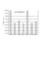
図2に、比較例1〜3、実施例1〜4の半導体薄膜(厚さ15nmのIn−Sn−Zn−O膜)のシート抵抗の測定結果を示す。比較例1に示すプラズマ処理なしのIn−Sn−Zn−O膜は高いシート抵抗値を示しているが、Arプラズマ処理を施したIn−Sn−Zn−O膜(比較例2、3)及び水蒸気プラズマ処理を施したIn−Sn−Zn−O膜(実施例1〜4)はともに、プラズマ処理なしの比較例1に対して大幅に抵抗値が低減している。また、水蒸気プラズマ処理とArプラズマ処理の効果を比較すると、水蒸気プラズマ処理は、Arプラズマ処理と比べて、ほぼ同等の酸化物半導体膜の抵抗低減効果を有しているが、実施例2のみは他の実施例と異なる傾向を示している。 FIG. 2 shows the measurement results of the sheet resistance of the semiconductor thin films (In-Sn—Zn—O film having a thickness of 15 nm) of Comparative Examples 1 to 3 and Examples 1 to 4. The In-Sn-Zn-O film without plasma treatment shown in Comparative Example 1 shows a high sheet resistance value, but the In-Sn-Zn-O film subjected to Ar plasma treatment (Comparative Examples 2 and 3) and Both the In-Sn-Zn-O films (Examples 1 to 4) subjected to the steam plasma treatment have a significantly reduced resistance value as compared with Comparative Example 1 without the plasma treatment. Further, comparing the effects of the steam plasma treatment and the Ar plasma treatment, the steam plasma treatment has almost the same resistance reduction effect of the oxide semiconductor film as that of the Ar plasma treatment, but only in Example 2 It shows a different tendency from the other examples.
−−− 厚さ50nmのIn−Sn−Zn−O膜の場合 −−−
厚さ50nmのIn−Sn−Zn−O膜に対して、それぞれ異なる処理を行い、処理後のシート抵抗を測定した。それぞれの膜の処理条件は、次のとおりである。--- In the case of In-Sn-Zn-O film with a thickness of 50 nm ---
The In-Sn-Zn-O film having a thickness of 50 nm was subjected to different treatments, and the sheet resistance after the treatment was measured. The treatment conditions for each film are as follows.
[比較例4]
・加熱後のプラズマ処理条件:プラズマ処理なし[Comparative Example 4]
・ Plasma treatment conditions after heating: No plasma treatment
[比較例5]
・加熱後のプラズマ処理条件(Arプラズマ処理):
ガス種:アルゴン
ガス流量:20sccm
In−Sn−Zn−O膜の載置位置:RFパワーを印加する電極上
RFパワー:150W
プラズマ処理時間:1分間[Comparative Example 5]
-Plasma treatment conditions after heating (Ar plasma treatment):
Gas type: Argon
Gas flow rate: 20 sccm
Placement position of In-Sn-Zn-O film: On the electrode to which RF power is applied
RF power: 150W
Plasma processing time: 1 minute
[比較例6]
・加熱後のプラズマ処理条件(Arプラズマ処理):
ガス種:アルゴン
ガス流量:20sccm
In−Sn−Zn−O膜の載置位置:RFパワーを印加する電極上
RFパワー:150W
プラズマ処理時間:10分間[Comparative Example 6]
-Plasma treatment conditions after heating (Ar plasma treatment):
Gas type: Argon
Gas flow rate: 20 sccm
Placement position of In-Sn-Zn-O film: On the electrode to which RF power is applied
RF power: 150W
Plasma processing time: 10 minutes
[実施例5]
・加熱後のプラズマ処理条件(水蒸気プラズマ処理):
ガス種:水蒸気
ガス流量:12sccm
In−Sn−Zn−O膜の載置位置:RFパワーを印加する電極上
RFパワー:250W
プラズマ処理時間:1分間[Example 5]
-Plasma treatment conditions after heating (steam plasma treatment):
Gas type: water vapor
Gas flow rate: 12 sccm
Placement position of In-Sn-Zn-O film: On the electrode to which RF power is applied
RF power: 250W
Plasma processing time: 1 minute
[実施例6]
・加熱後のプラズマ処理条件(水蒸気プラズマ処理):
ガス種:水蒸気
ガス流量:12sccm
In−Sn−Zn−O膜の載置位置:RFパワーを印加する電極上
RFパワー:250W
プラズマ処理時間:10分間[Example 6]
-Plasma treatment conditions after heating (steam plasma treatment):
Gas type: water vapor
Gas flow rate: 12 sccm
Placement position of In-Sn-Zn-O film: On the electrode to which RF power is applied
RF power: 250W
Plasma processing time: 10 minutes
[実施例7]
・加熱後のプラズマ処理条件(水蒸気プラズマ処理):
ガス種:水蒸気
ガス流量:12sccm
In−Sn−Zn−O膜の載置位置:接地電極上
RFパワー:250W
プラズマ処理時間:1分間[Example 7]
-Plasma treatment conditions after heating (steam plasma treatment):
Gas type: water vapor
Gas flow rate: 12 sccm
Placement position of In-Sn-Zn-O film: On the ground electrode
RF power: 250W
Plasma processing time: 1 minute
[実施例8]
・加熱後のプラズマ処理条件(水蒸気プラズマ処理):
ガス種:水蒸気
ガス流量:12sccm
In−Sn−Zn−O膜の載置位置:接地電極上
RFパワー:250W
プラズマ処理時間:10分間[Example 8]
-Plasma treatment conditions after heating (steam plasma treatment):
Gas type: water vapor
Gas flow rate: 12 sccm
Placement position of In-Sn-Zn-O film: On the ground electrode
RF power: 250W
Plasma processing time: 10 minutes
各条件における処理後のシート抵抗を、表2に示す。 Table 2 shows the sheet resistance after the treatment under each condition.
図3に、比較例4〜6、実施例5〜8の半導体薄膜(厚さ50nmのIn−Sn−Zn−O膜)のシート抵抗の測定結果を示す。比較例4に示すプラズマ処理なしのIn−Sn−Zn−O膜は高いシート抵抗値を示しているが、Arプラズマ処理を施したIn−Sn−Zn−O膜(比較例5、6)及び水蒸気プラズマ処理を施したIn−Sn−Zn−O膜(実施例5〜8)はともに、プラズマ処理なしの比較例4に対して大幅に抵抗値が低減している。また、水蒸気プラズマ処理とArプラズマ処理の効果を比較すると、水蒸気プラズマ処理は、Arプラズマ処理と比べて、ほぼ同等の酸化物半導体膜の抵抗低減効果を有していることを示している。 FIG. 3 shows the measurement results of the sheet resistance of the semiconductor thin films (In-Sn-Zn-O film having a thickness of 50 nm) of Comparative Examples 4 to 6 and Examples 5 to 8. The In-Sn-Zn-O film without plasma treatment shown in Comparative Example 4 shows a high sheet resistance value, but the In-Sn-Zn-O film subjected to Ar plasma treatment (Comparative Examples 5 and 6) and Both the In-Sn-Zn-O films (Examples 5 to 8) subjected to the steam plasma treatment have significantly reduced resistance values as compared with Comparative Example 4 without the plasma treatment. Further, comparing the effects of the steam plasma treatment and the Ar plasma treatment, it is shown that the steam plasma treatment has almost the same resistance reducing effect of the oxide semiconductor film as that of the Ar plasma treatment.
−−− 厚さ100nmのIn−Sn−Zn−O膜の場合 −−−
厚さ100nmのIn−Sn−Zn−O膜に対して、それぞれ異なる処理を行い、処理後のシート抵抗を測定した。それぞれの膜の処理条件は、次のとおりである。--- In the case of In-Sn-Zn-O film with a thickness of 100 nm ---
The In-Sn-Zn-O film having a thickness of 100 nm was subjected to different treatments, and the sheet resistance after the treatment was measured. The treatment conditions for each film are as follows.
[比較例7]
・加熱後のプラズマ処理条件:プラズマ処理なし[Comparative Example 7]
・ Plasma treatment conditions after heating: No plasma treatment
[比較例8]
・加熱後のプラズマ処理条件(Arプラズマ処理):
ガス種:アルゴン
ガス流量:20sccm
In−Sn−Zn−O膜の載置位置:RFパワーを印加する電極上
RFパワー:150W
プラズマ処理時間:1分間[Comparative Example 8]
-Plasma treatment conditions after heating (Ar plasma treatment):
Gas type: Argon
Gas flow rate: 20 sccm
Placement position of In-Sn-Zn-O film: On the electrode to which RF power is applied
RF power: 150W
Plasma processing time: 1 minute
[比較例9]
・加熱後のプラズマ処理条件(Arプラズマ処理):
ガス種:アルゴン
ガス流量:20sccm
In−Sn−Zn−O膜の載置位置:RFパワーを印加する電極上
RFパワー:150W
プラズマ処理時間:10分間[Comparative Example 9]
-Plasma treatment conditions after heating (Ar plasma treatment):
Gas type: Argon
Gas flow rate: 20 sccm
Placement position of In-Sn-Zn-O film: On the electrode to which RF power is applied
RF power: 150W
Plasma processing time: 10 minutes
[実施例9]
・加熱後のプラズマ処理条件(水蒸気プラズマ処理):
ガス種:水蒸気
ガス流量:12sccm
In−Sn−Zn−O膜の載置位置:RFパワーを印加する電極上
RFパワー:250W
プラズマ処理時間:1分間[Example 9]
-Plasma treatment conditions after heating (steam plasma treatment):
Gas type: water vapor
Gas flow rate: 12 sccm
Placement position of In-Sn-Zn-O film: On the electrode to which RF power is applied
RF power: 250W
Plasma processing time: 1 minute
[実施例10]
・加熱後のプラズマ処理条件(水蒸気プラズマ処理):
ガス種:水蒸気
ガス流量:12sccm
In−Sn−Zn−O膜の載置位置:RFパワーを印加する電極上
RFパワー:250W
プラズマ処理時間:10分間[Example 10]
-Plasma treatment conditions after heating (steam plasma treatment):
Gas type: water vapor
Gas flow rate: 12 sccm
Placement position of In-Sn-Zn-O film: On the electrode to which RF power is applied
RF power: 250W
Plasma processing time: 10 minutes
[実施例11]
・加熱後のプラズマ処理条件(水蒸気プラズマ処理):
ガス種:水蒸気
ガス流量:12sccm
In−Sn−Zn−O膜の載置位置:接地電極上
RFパワー:250W
プラズマ処理時間:1分間[Example 11]
-Plasma treatment conditions after heating (steam plasma treatment):
Gas type: water vapor
Gas flow rate: 12 sccm
Placement position of In-Sn-Zn-O film: On the ground electrode
RF power: 250W
Plasma processing time: 1 minute
[実施例12]
・加熱後のプラズマ処理条件(水蒸気プラズマ処理):
ガス種:水蒸気
ガス流量:12sccm
In−Sn−Zn−O膜の載置位置:接地電極上
RFパワー:250W
プラズマ処理時間:10分間[Example 12]
-Plasma treatment conditions after heating (steam plasma treatment):
Gas type: water vapor
Gas flow rate: 12 sccm
Placement position of In-Sn-Zn-O film: On the ground electrode
RF power: 250W
Plasma processing time: 10 minutes
各条件における処理後のシート抵抗を、表3に示す。 Table 3 shows the sheet resistance after the treatment under each condition.
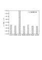
図4に、比較例7〜9、実施例9〜12の半導体薄膜(厚さ100nmのIn−Sn−Zn−O膜)のシート抵抗の測定結果を示す。比較例7に示すプラズマ処理なしのIn−Sn−Zn−O膜は高いシート抵抗値を示しているが、Arプラズマ処理を施したIn−Sn−Zn−O膜(比較例8、9)及び水蒸気プラズマ処理を施したIn−Sn−Zn−O膜(実施例9〜12)はともに、プラズマ処理なしの比較例7に対して大幅に抵抗値が低減している。また、水蒸気プラズマ処理とArプラズマ処理の効果を比較すると、水蒸気プラズマ処理は、Arプラズマ処理と比べて、ほぼ同等の酸化物半導体膜の抵抗低減効果を有していることを示している。 FIG. 4 shows the measurement results of the sheet resistance of the semiconductor thin films (In-Sn-Zn-O film having a thickness of 100 nm) of Comparative Examples 7 to 9 and Examples 9 to 12. The In-Sn-Zn-O film without plasma treatment shown in Comparative Example 7 shows a high sheet resistance value, but the In-Sn-Zn-O film subjected to Ar plasma treatment (Comparative Examples 8 and 9) and Both the In—Sn—Zn—O films (Examples 9 to 12) subjected to the steam plasma treatment have significantly reduced resistance values as compared with Comparative Example 7 without the plasma treatment. Further, comparing the effects of the steam plasma treatment and the Ar plasma treatment, it is shown that the steam plasma treatment has almost the same resistance reducing effect of the oxide semiconductor film as that of the Ar plasma treatment.
実施例1〜12から、いずれの厚さの酸化物半導体膜も、未処理のものと比較して、水蒸気プラズマ処理によりシート抵抗値が低減する。このシート抵抗値は、半導体装置における電極・配線、又はトランジスタのソース・ドレイン領域等の導電領域として使用するのに十分な、低い抵抗値である。実際の製造プロセスにおいては、酸化物半導体膜を所定の形状にパターンニングして、又は、低抵抗化の不要な部分をマスクし酸化物半導体膜の所定の領域を露出させて、水蒸気プラズマに晒し、導電領域を形成する。なお、In−Sn−Zn−O膜等の酸化物半導体膜は、可視光を透過させるため、水蒸気プラズマ処理した酸化物半導体膜を透明電極・透明配線として、使用することができる。 From Examples 1 to 12, the sheet resistance value of the oxide semiconductor film of any thickness is reduced by the steam plasma treatment as compared with the untreated one. This sheet resistance value is a low resistance value sufficient to be used as a conductive region such as an electrode / wiring in a semiconductor device or a source / drain region of a transistor. In the actual manufacturing process, the oxide semiconductor film is patterned into a predetermined shape, or the unnecessary portion of the resistance reduction is masked to expose a predetermined region of the oxide semiconductor film, and the oxide semiconductor film is exposed to steam plasma. , Form a conductive region. Since an oxide semiconductor film such as an In-Sn-Zn-O film transmits visible light, the oxide semiconductor film treated with steam plasma can be used as a transparent electrode / transparent wiring.
図3、図4を参照すると、全体として処理時間が1分間の場合よりも10分間の場合の方が、シート抵抗値が低いことから、水蒸気プラズマが処理時間と共に酸化物半導体膜により浸透するものと推測される。 With reference to FIGS. 3 and 4, since the sheet resistance value is lower when the processing time is 10 minutes than when the processing time is 1 minute as a whole, the water vapor plasma permeates through the oxide semiconductor film with the processing time. It is presumed.
膜が均質であればシート抵抗値は膜厚が厚くなるほど低くなるところ、厚さ15nmの半導体膜のシート抵抗値よりも厚さ50nmの半導体膜のシート抵抗値が低いことから、水素プラズマは50nm以上浸透しているものと推測される。一方、厚さ50nmの半導体膜のシート抵抗値と厚さ100nmの半導体膜のシート抵抗値とがほぼ変わらないことから、100nmの深さまでは水蒸気プラズマが十分浸透していない可能性もある。厚い酸化物半導体膜は、プラズマ処理時間を長くすることにより、更に低抵抗化が可能と推定される。 If the film is homogeneous, the sheet resistance value decreases as the film thickness increases. However, since the sheet resistance value of the semiconductor film having a thickness of 50 nm is lower than the sheet resistance value of the semiconductor film having a thickness of 15 nm, the hydrogen plasma has a thickness of 50 nm. It is presumed that the above has penetrated. On the other hand, since the sheet resistance value of the semiconductor film having a thickness of 50 nm and the sheet resistance value of the semiconductor film having a thickness of 100 nm are almost the same, there is a possibility that the steam plasma does not sufficiently permeate at a depth of 100 nm. It is presumed that the thick oxide semiconductor film can further reduce the resistance by lengthening the plasma treatment time.
別の実験によれば、水蒸気プラズマは、金属へのダメージは殆ど発生しない。しかしながら、実施例1〜12を比較すると、厚さが薄い(15nm)酸化物半導体膜をRF電極2上に載置して10分間のプラズマを照射した場合(実施例2)には、接地電極3上に載置した場合よりシート抵抗値が低下していないことから、RF電極2上で長時間のプラズマを照射した場合には、酸化物半導体膜に若干のダメージが生じる可能性があると推測される。したがって、低抵抗化の水素プラズマ処理は、基板を接地電極に載置して処理することが望ましい。 According to another experiment, water vapor plasma causes almost no damage to metals. However, comparing Examples 1 to 12, when a thin (15 nm) oxide semiconductor film is placed on the
[In−Ga−Zn−O(IGZO)膜に対するプラズマ処理]
[製膜処理]
ガラス基板上に、酸化インジウムガリウム亜鉛(In−Ga−Zn−O)の酸化物半導体膜をスパッタリング法で製膜した。製膜条件は、スパッタターゲット(In−Ga−Zn−Oターゲット)に印加する電力の値はRF100W、ガスの流量比はAr/O2=19.4/0.6sccm、圧力は0.4Paとした。本実施例で使用したスパッタターゲットの組成は、In:Ga:Zn:O=1:1:1:4である(原子数比)。なお、酸化インジウムガリウム亜鉛の組成は、これ以外の任意の組成比であってよい。[Plasma treatment for In-Ga-Zn-O (IGZO) film]
[Film formation process]
An oxide semiconductor film of indium gallium zinc oxide (In-Ga-Zn-O) was formed on a glass substrate by a sputtering method. As for the film forming conditions, the value of the electric power applied to the sputter target (In-Ga-Zn-O target) is RF100W, the gas flow rate ratio is Ar / O2 = 19.4 / 0.6sccm, and the pressure is 0.4Pa. did. The composition of the sputtering target used in this example is In: Ga: Zn: O = 1: 1: 1: 4 (atomic number ratio). The composition of indium gallium zinc oxide may be any other composition ratio.
また、製膜時間を変えることで、膜厚の異なる3種類のIn−Ga−Zn−O膜(膜厚15nm、50nm、100nmの3種類)を形成した。その後、ホットプレートを用いて、大気中で300℃、1時間の熱処理を実施した。 Further, by changing the film forming time, three types of In-Ga-Zn-O films having different film thicknesses (three types having a film thickness of 15 nm, 50 nm, and 100 nm) were formed. Then, using a hot plate, heat treatment was carried out in the air at 300 ° C. for 1 hour.
[プラズマ処理]
製膜し加熱処理を行ったIn−Ga−Zn−O膜に対して、Arプラズマ処理、又は、水蒸気プラズマ処理を行った。なお、比較のために、プラズマ処理を行わないIn−Ga−Zn−O膜も準備した。[Plasma processing]
The In-Ga-Zn-O film that had been formed and heat-treated was subjected to Ar plasma treatment or steam plasma treatment. For comparison, an In-Ga-Zn-O film that was not subjected to plasma treatment was also prepared.
[抵抗測定]
プラズマ処理なしのIn−Ga−Zn−O膜(比較例10、13、16)、Arプラズマ処理したIn−Ga−Zn−O膜(比較例11,12、14、15、17、18)、及び、水蒸気プラズマ処理したIn−Ga−Zn−O膜(実施例13〜24)について、シート抵抗を4探針法で測定した。[Resistance measurement]
In-Ga-Zn-O film without plasma treatment (Comparative Examples 10, 13, 16), In-Ga-Zn-O film treated with Ar plasma (Comparative Examples 11, 12, 14, 15, 17, 18), The sheet resistance of the In-Ga-Zn-O film (Examples 13 to 24) treated with steam plasma was measured by a 4-probe method.
−−− 厚さ15nmのIn−Ga−Zn−O膜の場合 −−−
厚さ15nmのIn−Ga−Zn−O膜に対して、それぞれ異なる処理を行い、処理後のシート抵抗を測定した。それぞれの膜の処理条件は、次のとおりである。--- In the case of In-Ga-Zn-O film with a thickness of 15 nm ---
The In-Ga-Zn-O film having a thickness of 15 nm was subjected to different treatments, and the sheet resistance after the treatment was measured. The treatment conditions for each film are as follows.
[比較例10]
・加熱後のプラズマ処理条件:プラズマ処理なし[Comparative Example 10]
・ Plasma treatment conditions after heating: No plasma treatment
[比較例11]
・加熱後のプラズマ処理条件(Arプラズマ処理):
ガス種:アルゴン
ガス流量:20sccm
In−Ga−Zn−O膜の載置位置:RFパワーを印加する電極上
RFパワー:150W
プラズマ処理時間:1分間[Comparative Example 11]
-Plasma treatment conditions after heating (Ar plasma treatment):
Gas type: Argon
Gas flow rate: 20 sccm
Placement position of In-Ga-Zn-O film: On the electrode to which RF power is applied
RF power: 150W
Plasma processing time: 1 minute
[比較例12]
・加熱後のプラズマ処理条件(Arプラズマ処理):
ガス種:アルゴン
ガス流量:20sccm
In−Ga−Zn−O膜の載置位置:RFパワーを印加する電極上
RFパワー:150W
プラズマ処理時間:10分間[Comparative Example 12]
-Plasma treatment conditions after heating (Ar plasma treatment):
Gas type: Argon
Gas flow rate: 20 sccm
Placement position of In-Ga-Zn-O film: On the electrode to which RF power is applied
RF power: 150W
Plasma processing time: 10 minutes
[実施例13]
・加熱後のプラズマ処理条件(水蒸気プラズマ処理):
ガス種:水蒸気
ガス流量:12sccm
In−Ga−Zn−O膜の載置位置:RFパワーを印加する電極上
RFパワー:250W
プラズマ処理時間:1分間[Example 13]
-Plasma treatment conditions after heating (steam plasma treatment):
Gas type: water vapor
Gas flow rate: 12 sccm
Placement position of In-Ga-Zn-O film: On the electrode to which RF power is applied
RF power: 250W
Plasma processing time: 1 minute
[実施例14]
・加熱後のプラズマ処理条件(水蒸気プラズマ処理):
ガス種:水蒸気
ガス流量:12sccm
In−Ga−Zn−O膜の載置位置:RFパワーを印加する電極上
RFパワー:250W
プラズマ処理時間:10分間[Example 14]
-Plasma treatment conditions after heating (steam plasma treatment):
Gas type: water vapor
Gas flow rate: 12 sccm
Placement position of In-Ga-Zn-O film: On the electrode to which RF power is applied
RF power: 250W
Plasma processing time: 10 minutes
[実施例15]
・加熱後のプラズマ処理条件(水蒸気プラズマ処理):
ガス種:水蒸気
ガス流量:12sccm
In−Ga−Zn−O膜の載置位置:接地電極上
RFパワー:250W
プラズマ処理時間:1分間[Example 15]
-Plasma treatment conditions after heating (steam plasma treatment):
Gas type: water vapor
Gas flow rate: 12 sccm
Placement position of In-Ga-Zn-O film: On the ground electrode
RF power: 250W
Plasma processing time: 1 minute
[実施例16]
・加熱後のプラズマ処理条件(水蒸気プラズマ処理):
ガス種:水蒸気
ガス流量:12sccm
In−Ga−Zn−O膜の載置位置:接地電極上
RFパワー:250W
プラズマ処理時間:10分間[Example 16]
-Plasma treatment conditions after heating (steam plasma treatment):
Gas type: water vapor
Gas flow rate: 12 sccm
Placement position of In-Ga-Zn-O film: On the ground electrode
RF power: 250W
Plasma processing time: 10 minutes
各条件における処理後のシート抵抗を、表4に示す。 Table 4 shows the sheet resistance after the treatment under each condition.
図5に、比較例10〜12、実施例13〜16の半導体薄膜(厚さ15nmのIn−Ga−Zn−O膜)のシート抵抗の測定結果を示す。比較例10に示すプラズマ処理なしのIn−Ga−Zn−O膜は高いシート抵抗値を示しているが、Arプラズマ処理を施したIn−Ga−Zn−O膜(比較例11、12)及び水蒸気プラズマ処理を施したIn−Ga−Zn−O膜(実施例13、15、16)はともに、プラズマ処理なしの比較例10に対して大幅に抵抗値が低減している。また、水蒸気プラズマ処理とArプラズマ処理の効果を比較すると、水蒸気プラズマ処理は、Arプラズマ処理と比べて、同等またはそれ以上の酸化物半導体膜の抵抗低減効果を有していることを示している。なお、実施例14は、特異的に高い抵抗値を示しているが、RF電極2上でのプラズマ照射により、酸化物半導体膜にダメージが生じた可能性がある。 FIG. 5 shows the measurement results of the sheet resistance of the semiconductor thin films (In-Ga-Zn-O film having a thickness of 15 nm) of Comparative Examples 10 to 12 and Examples 13 to 16. The In-Ga-Zn-O film without plasma treatment shown in Comparative Example 10 shows a high sheet resistance value, but the In-Ga-Zn-O film subjected to Ar plasma treatment (Comparative Examples 11 and 12) and Both the In-Ga-Zn-O films (Examples 13, 15 and 16) subjected to the steam plasma treatment have significantly reduced resistance values as compared with Comparative Example 10 without the plasma treatment. Further, comparing the effects of the steam plasma treatment and the Ar plasma treatment, it is shown that the steam plasma treatment has an effect of reducing the resistance of the oxide semiconductor film equal to or higher than that of the Ar plasma treatment. .. Although Example 14 shows a specifically high resistance value, it is possible that the oxide semiconductor film was damaged by plasma irradiation on the
−−− 厚さ50nmのIn−Ga−Zn−O膜の場合 −−−
厚さ50nmのIn−Ga−Zn−O膜に対して、それぞれ異なる処理を行い、処理後のシート抵抗を測定した。それぞれの膜の処理条件は、次のとおりである。--- In the case of In-Ga-Zn-O film with a thickness of 50 nm ---
The In-Ga-Zn-O film having a thickness of 50 nm was subjected to different treatments, and the sheet resistance after the treatment was measured. The treatment conditions for each film are as follows.
[比較例13]
・加熱後のプラズマ処理条件:プラズマ処理なし[Comparative Example 13]
・ Plasma treatment conditions after heating: No plasma treatment
[比較例14]
・加熱後のプラズマ処理条件(Arプラズマ処理):
ガス種:アルゴン
ガス流量:20sccm
In−Ga−Zn−O膜の載置位置:RFパワーを印加する電極上
RFパワー:150W
プラズマ処理時間:1分間[Comparative Example 14]
-Plasma treatment conditions after heating (Ar plasma treatment):
Gas type: Argon
Gas flow rate: 20 sccm
Placement position of In-Ga-Zn-O film: On the electrode to which RF power is applied
RF power: 150W
Plasma processing time: 1 minute
[比較例15]
・加熱後のプラズマ処理条件(Arプラズマ処理):
ガス種:アルゴン
ガス流量:20sccm
In−Ga−Zn−O膜の載置位置:RFパワーを印加する電極上
RFパワー:150W
プラズマ処理時間:10分間[Comparative Example 15]
-Plasma treatment conditions after heating (Ar plasma treatment):
Gas type: Argon
Gas flow rate: 20 sccm
Placement position of In-Ga-Zn-O film: On the electrode to which RF power is applied
RF power: 150W
Plasma processing time: 10 minutes
[実施例17]
・加熱後のプラズマ処理条件(水蒸気プラズマ処理):
ガス種:水蒸気
ガス流量:12sccm
In−Ga−Zn−O膜の載置位置:RFパワーを印加する電極上
RFパワー:250W
プラズマ処理時間:1分間[Example 17]
-Plasma treatment conditions after heating (steam plasma treatment):
Gas type: water vapor
Gas flow rate: 12 sccm
Placement position of In-Ga-Zn-O film: On the electrode to which RF power is applied
RF power: 250W
Plasma processing time: 1 minute
[実施例18]
・加熱後のプラズマ処理条件(水蒸気プラズマ処理):
ガス種:水蒸気
ガス流量:12sccm
In−Ga−Zn−O膜の載置位置:RFパワーを印加する電極上
RFパワー:250W
プラズマ処理時間:10分間[Example 18]
-Plasma treatment conditions after heating (steam plasma treatment):
Gas type: water vapor
Gas flow rate: 12 sccm
Placement position of In-Ga-Zn-O film: On the electrode to which RF power is applied
RF power: 250W
Plasma processing time: 10 minutes
[実施例19]
・加熱後のプラズマ処理条件(水蒸気プラズマ処理):
ガス種:水蒸気
ガス流量:12sccm
In−Ga−Zn−O膜の載置位置:接地電極上
RFパワー:250W
プラズマ処理時間:1分間[Example 19]
-Plasma treatment conditions after heating (steam plasma treatment):
Gas type: water vapor
Gas flow rate: 12 sccm
Placement position of In-Ga-Zn-O film: On the ground electrode
RF power: 250W
Plasma processing time: 1 minute
[実施例20]
・加熱後のプラズマ処理条件(水蒸気プラズマ処理):
ガス種:水蒸気
ガス流量:12sccm
In−Ga−Zn−O膜の載置位置:接地電極上
RFパワー:250W
プラズマ処理時間:10分間[Example 20]
-Plasma treatment conditions after heating (steam plasma treatment):
Gas type: water vapor
Gas flow rate: 12 sccm
Placement position of In-Ga-Zn-O film: On the ground electrode
RF power: 250W
Plasma processing time: 10 minutes
各条件における処理後のシート抵抗を、表5に示す。 Table 5 shows the sheet resistance after the treatment under each condition.
図6に、比較例13〜15、実施例17〜20の半導体薄膜(厚さ50nmのIn−Ga−Zn−O膜)のシート抵抗の測定結果を示す。比較例13に示すプラズマ処理なしのIn−Ga−Zn−O膜は高いシート抵抗値を示しているが、Arプラズマ処理を施したIn−Ga−Zn−O膜(比較例14、15)及び水蒸気プラズマ処理を施したIn−Ga−Zn−O膜(実施例17〜20)はともに、プラズマ処理なしの比較例13に対して大幅に抵抗値が低減している。また、水蒸気プラズマ処理とArプラズマ処理の効果を比較すると、水蒸気プラズマ処理は、Arプラズマ処理と比べて、同等またはそれ以上の酸化物半導体膜の抵抗低減効果を有していることを示している。 FIG. 6 shows the measurement results of the sheet resistance of the semiconductor thin films (In-Ga-Zn-O film having a thickness of 50 nm) of Comparative Examples 13 to 15 and Examples 17 to 20. The In-Ga-Zn-O film without plasma treatment shown in Comparative Example 13 shows a high sheet resistance value, but the In-Ga-Zn-O film subjected to Ar plasma treatment (Comparative Examples 14 and 15) and Both the In-Ga-Zn-O films (Examples 17 to 20) subjected to the steam plasma treatment have a significantly reduced resistance value as compared with Comparative Example 13 without the plasma treatment. Further, comparing the effects of the steam plasma treatment and the Ar plasma treatment, it is shown that the steam plasma treatment has an effect of reducing the resistance of the oxide semiconductor film equal to or higher than that of the Ar plasma treatment. ..
−−− 厚さ100nmのIn−Ga−Zn−O膜の場合 −−−
厚さ100nmのIn−Ga−Zn−O膜に対して、それぞれ異なる処理を行い、処理後のシート抵抗を測定した。それぞれの膜の処理条件は、次のとおりである。--- In the case of In-Ga-Zn-O film with a thickness of 100 nm ---
The In-Ga-Zn-O film having a thickness of 100 nm was subjected to different treatments, and the sheet resistance after the treatment was measured. The treatment conditions for each film are as follows.
[比較例16]
・加熱後のプラズマ処理条件:プラズマ処理なし[Comparative Example 16]
・ Plasma treatment conditions after heating: No plasma treatment
[比較例17]
・加熱後のプラズマ処理条件(Arプラズマ処理):
ガス種:アルゴン
ガス流量:20sccm
In−Ga−Zn−O膜の載置位置:RFパワーを印加する電極上
RFパワー:150W
プラズマ処理時間:1分間[Comparative Example 17]
-Plasma treatment conditions after heating (Ar plasma treatment):
Gas type: Argon
Gas flow rate: 20 sccm
Placement position of In-Ga-Zn-O film: On the electrode to which RF power is applied
RF power: 150W
Plasma processing time: 1 minute
[比較例18]
・加熱後のプラズマ処理条件(Arプラズマ処理):
ガス種:アルゴン
ガス流量:20sccm
In−Ga−Zn−O膜の載置位置:RFパワーを印加する電極上
RFパワー:150W
プラズマ処理時間:10分間[Comparative Example 18]
-Plasma treatment conditions after heating (Ar plasma treatment):
Gas type: Argon
Gas flow rate: 20 sccm
Placement position of In-Ga-Zn-O film: On the electrode to which RF power is applied
RF power: 150W
Plasma processing time: 10 minutes
[実施例21]
・加熱後のプラズマ処理条件(水蒸気プラズマ処理):
ガス種:水蒸気
ガス流量:12sccm
In−Ga−Zn−O膜の載置位置:RFパワーを印加する電極上
RFパワー:250W
プラズマ処理時間:1分間[Example 21]
-Plasma treatment conditions after heating (steam plasma treatment):
Gas type: water vapor
Gas flow rate: 12 sccm
Placement position of In-Ga-Zn-O film: On the electrode to which RF power is applied
RF power: 250W
Plasma processing time: 1 minute
[実施例22]
・加熱後のプラズマ処理条件(水蒸気プラズマ処理):
ガス種:水蒸気
ガス流量:12sccm
In−Ga−Zn−O膜の載置位置:RFパワーを印加する電極上
RFパワー:250W
プラズマ処理時間:10分間[Example 22]
-Plasma treatment conditions after heating (steam plasma treatment):
Gas type: water vapor
Gas flow rate: 12 sccm
Placement position of In-Ga-Zn-O film: On the electrode to which RF power is applied
RF power: 250W
Plasma processing time: 10 minutes
[実施例23]
・加熱後のプラズマ処理条件(水蒸気プラズマ処理):
ガス種:水蒸気
ガス流量:12sccm
In−Ga−Zn−O膜の載置位置:接地電極上
RFパワー:250W
プラズマ処理時間:1分間[Example 23]
-Plasma treatment conditions after heating (steam plasma treatment):
Gas type: water vapor
Gas flow rate: 12 sccm
Placement position of In-Ga-Zn-O film: On the ground electrode
RF power: 250W
Plasma processing time: 1 minute
[実施例24]
・加熱後のプラズマ処理条件(水蒸気プラズマ処理):
ガス種:水蒸気
ガス流量:12sccm
In−Ga−Zn−O膜の載置位置:接地電極上
RFパワー:250W
プラズマ処理時間:10分間[Example 24]
-Plasma treatment conditions after heating (steam plasma treatment):
Gas type: water vapor
Gas flow rate: 12 sccm
Placement position of In-Ga-Zn-O film: On the ground electrode
RF power: 250W
Plasma processing time: 10 minutes
各条件における処理後のシート抵抗を、表6に示す。 Table 6 shows the sheet resistance after the treatment under each condition.
図7に、比較例16〜18、実施例21〜24の半導体薄膜(厚さ100nmのIn−Ga−Zn−O膜)のシート抵抗の測定結果を示す。比較例16に示すプラズマ処理なしのIn−Ga−Zn−O膜は高いシート抵抗値を示しているが、Arプラズマ処理を施したIn−Ga−Zn−O膜(比較例17、18)及び水蒸気プラズマ処理を施したIn−Ga−Zn−O膜(実施例21〜24)はともに、プラズマ処理なしの比較例16に対して大幅に抵抗値が低減している。また、水蒸気プラズマ処理とArプラズマ処理の効果を比較すると、水蒸気プラズマ処理は、Arプラズマ処理と比べて、同等またはそれ以上の酸化物半導体膜の抵抗低減効果を有していることを示している。 FIG. 7 shows the measurement results of the sheet resistance of the semiconductor thin films (In-Ga-Zn-O film having a thickness of 100 nm) of Comparative Examples 16 to 18 and Examples 21 to 24. The In-Ga-Zn-O film without plasma treatment shown in Comparative Example 16 shows a high sheet resistance value, but the In-Ga-Zn-O film subjected to Ar plasma treatment (Comparative Examples 17 and 18) and Both the In-Ga-Zn-O films (Examples 21 to 24) subjected to the steam plasma treatment have significantly reduced resistance values as compared with Comparative Example 16 without the plasma treatment. Further, comparing the effects of the steam plasma treatment and the Ar plasma treatment, it is shown that the steam plasma treatment has an effect of reducing the resistance of the oxide semiconductor film equal to or higher than that of the Ar plasma treatment. ..
[In−Sn−O(ITO)膜に対するプラズマ処理]
[製膜処理]
ガラス基板上に、酸化インジウムスズ(In−Sn−O)の酸化物半導体膜をスパッタリング法で製膜した。製膜条件は、スパッタターゲット(In−Sn−Oターゲット)に印加する電力の値はRF250W、ガスの流量比はAr/O2=45/0.3sccm、圧力は0.9Paとした。本実施例で使用したスパッタターゲットの組成は、In2O3=90wt%,SnO2=10wt%である。なお、酸化インジウムスズの組成は、これ以外の任意の組成比であってよい。[Plasma treatment for In-Sn-O (ITO) film]
[Film formation process]
An oxide semiconductor film of indium tin oxide (In—Sn—O) was formed on a glass substrate by a sputtering method. The film forming conditions were that the value of the electric power applied to the sputter target (In-Sn-O target) was RF250W, the gas flow rate ratio was Ar / O2 = 45 / 0.3sccm, and the pressure was 0.9Pa. The composition of the sputtering target used in this example is In2 O3 = 90 wt% and SnO2 = 10 wt%. The composition of indium tin oxide may be any other composition ratio.
また、製膜時間を変えることで、膜厚の異なる3種類のIn−Sn−O膜(膜厚15nm、50nm、100nmの3種類)を形成した。その後、ホットプレートを用いて、大気中で300℃、1時間の熱処理を実施した。 Further, by changing the film forming time, three types of In-Sn-O films having different film thicknesses (three types having a film thickness of 15 nm, 50 nm, and 100 nm) were formed. Then, using a hot plate, heat treatment was carried out in the air at 300 ° C. for 1 hour.
[プラズマ処理]
製膜し加熱処理を行ったIn−Sn−O膜に対して、Arプラズマ処理、又は、水蒸気プラズマ処理を行った。なお、比較のために、プラズマ処理を行わないIn−Sn−O膜も準備した。[Plasma processing]
The In-Sn-O film formed and heat-treated was subjected to Ar plasma treatment or steam plasma treatment. For comparison, an In-Sn-O film that was not subjected to plasma treatment was also prepared.
[抵抗測定]
プラズマ処理なしのIn−Sn−O膜(比較例19、22、25)、Arプラズマ処理したIn−Sn−O膜(比較例20,21、23、24、26、27)、及び、水蒸気プラズマ処理したIn−Sn−O膜(実施例25〜36)について、シート抵抗を4探針法で測定した。[Resistance measurement]
In-Sn-O film without plasma treatment (Comparative Examples 19, 22, 25), In-Sn-O film treated with Ar plasma (Comparative Examples 20, 21, 23, 24, 26, 27), and steam plasma. The sheet resistance of the treated In—Sn—O films (Examples 25 to 36) was measured by a 4-probe method.
−−− 厚さ15nmのIn−Sn−O膜の場合 −−−
厚さ15nmのIn−Sn−O膜に対して、それぞれ異なる処理を行い、処理後のシート抵抗を測定した。それぞれの膜の処理条件は、次のとおりである。--- In the case of an In-Sn-O film with a thickness of 15 nm ---
The In—Sn—O film having a thickness of 15 nm was subjected to different treatments, and the sheet resistance after the treatment was measured. The treatment conditions for each film are as follows.
[比較例19]
・加熱後のプラズマ処理条件:プラズマ処理なし[Comparative Example 19]
・ Plasma treatment conditions after heating: No plasma treatment
[比較例20]
・加熱後のプラズマ処理条件(Arプラズマ処理):
ガス種:アルゴン
ガス流量:20sccm
In−Sn−O膜の載置位置:RFパワーを印加する電極上
RFパワー:150W
プラズマ処理時間:1分間[Comparative Example 20]
-Plasma treatment conditions after heating (Ar plasma treatment):
Gas type: Argon
Gas flow rate: 20 sccm
Placement position of In-Sn-O film: On the electrode to which RF power is applied
RF power: 150W
Plasma processing time: 1 minute
[比較例21]
・加熱後のプラズマ処理条件(Arプラズマ処理):
ガス種:アルゴン
ガス流量:20sccm
In−Sn−O膜の載置位置:RFパワーを印加する電極上
RFパワー:150W
プラズマ処理時間:10分間[Comparative Example 21]
-Plasma treatment conditions after heating (Ar plasma treatment):
Gas type: Argon
Gas flow rate: 20 sccm
Placement position of In-Sn-O film: On the electrode to which RF power is applied
RF power: 150W
Plasma processing time: 10 minutes
[実施例25]
・加熱後のプラズマ処理条件(水蒸気プラズマ処理):
ガス種:水蒸気
ガス流量:12sccm
In−Sn−O膜の載置位置:RFパワーを印加する電極上
RFパワー:250W
プラズマ処理時間:1分間[Example 25]
-Plasma treatment conditions after heating (steam plasma treatment):
Gas type: water vapor
Gas flow rate: 12 sccm
Placement position of In-Sn-O film: On the electrode to which RF power is applied
RF power: 250W
Plasma processing time: 1 minute
[実施例26]
・加熱後のプラズマ処理条件(水蒸気プラズマ処理):
ガス種:水蒸気
ガス流量:12sccm
In−Sn−O膜の載置位置:RFパワーを印加する電極上
RFパワー:250W
プラズマ処理時間:10分間[Example 26]
-Plasma treatment conditions after heating (steam plasma treatment):
Gas type: water vapor
Gas flow rate: 12 sccm
Placement position of In-Sn-O film: On the electrode to which RF power is applied
RF power: 250W
Plasma processing time: 10 minutes
[実施例27]
・加熱後のプラズマ処理条件(水蒸気プラズマ処理):
ガス種:水蒸気
ガス流量:12sccm
In−Sn−O膜の載置位置:接地電極上
RFパワー:250W
プラズマ処理時間:1分間[Example 27]
-Plasma treatment conditions after heating (steam plasma treatment):
Gas type: water vapor
Gas flow rate: 12 sccm
Placement position of In-Sn-O film: On the ground electrode
RF power: 250W
Plasma processing time: 1 minute
[実施例28]
・加熱後のプラズマ処理条件(水蒸気プラズマ処理):
ガス種:水蒸気
ガス流量:12sccm
In−Sn−O膜の載置位置:接地電極上
RFパワー:250W
プラズマ処理時間:10分間[Example 28]
-Plasma treatment conditions after heating (steam plasma treatment):
Gas type: water vapor
Gas flow rate: 12 sccm
Placement position of In-Sn-O film: On the ground electrode
RF power: 250W
Plasma processing time: 10 minutes
各条件における処理後のシート抵抗を、表7に示す。 Table 7 shows the sheet resistance after the treatment under each condition.
図8に、比較例19〜21、実施例25〜28の半導体薄膜(厚さ15nmのIn−Sn−O膜)のシート抵抗の測定結果を示す。In−Sn−O膜は、プラズマ処理を行わないもの(比較例19)であっても抵抗値が比較的低いが、Arプラズマ処理を施したIn−Sn−O膜(比較例20)及び水蒸気プラズマ処理を施したIn−Sn−O膜(実施例25、27、28)はともに、プラズマ処理なしの比較例19に対して更に抵抗値が低減している。また、水蒸気プラズマ処理とArプラズマ処理の効果を比較すると、水蒸気プラズマ処理は、Arプラズマ処理と比べて、同等またはそれ以上の酸化物半導体膜の抵抗低減効果を有していることを示している。なお、比較例21は特異的に高い抵抗値を示しているが、RF電極2上でのプラズマ照射により、酸化物半導体膜にダメージが生じた可能性がある。 FIG. 8 shows the measurement results of the sheet resistance of the semiconductor thin films (In—Sn—O film having a thickness of 15 nm) of Comparative Examples 19 to 21 and Examples 25 to 28. The In-Sn-O film has a relatively low resistance value even if it is not subjected to plasma treatment (Comparative Example 19), but the In-Sn-O film that has been subjected to Ar plasma treatment (Comparative Example 20) and water vapor. The resistance values of both the plasma-treated In—Sn—O films (Examples 25, 27, 28) are further reduced as compared with Comparative Example 19 without plasma treatment. Further, comparing the effects of the steam plasma treatment and the Ar plasma treatment, it is shown that the steam plasma treatment has an effect of reducing the resistance of the oxide semiconductor film equal to or higher than that of the Ar plasma treatment. .. Although Comparative Example 21 shows a specifically high resistance value, it is possible that the oxide semiconductor film was damaged by plasma irradiation on the
−−− 厚さ50nmのIn−Sn−O膜の場合 −−−
厚さ50nmのIn−Sn−O膜に対して、それぞれ異なる処理を行い、処理後のシート抵抗を測定した。それぞれの膜の処理条件は、次のとおりである。--- In the case of an In-Sn-O film with a thickness of 50 nm ---
The In—Sn—O film having a thickness of 50 nm was subjected to different treatments, and the sheet resistance after the treatment was measured. The treatment conditions for each film are as follows.
[比較例22]
・加熱後のプラズマ処理条件:プラズマ処理なし[Comparative Example 22]
・ Plasma treatment conditions after heating: No plasma treatment
[比較例23]
・加熱後のプラズマ処理条件(Arプラズマ処理):
ガス種:アルゴン
ガス流量:20sccm
In−Sn−O膜の載置位置:RFパワーを印加する電極上
RFパワー:150W
プラズマ処理時間:1分間[Comparative Example 23]
-Plasma treatment conditions after heating (Ar plasma treatment):
Gas type: Argon
Gas flow rate: 20 sccm
Placement position of In-Sn-O film: On the electrode to which RF power is applied
RF power: 150W
Plasma processing time: 1 minute
[比較例24]
・加熱後のプラズマ処理条件(Arプラズマ処理):
ガス種:アルゴン
ガス流量:20sccm
In−Sn−O膜の載置位置:RFパワーを印加する電極上
RFパワー:150W
プラズマ処理時間:10分間[Comparative Example 24]
-Plasma treatment conditions after heating (Ar plasma treatment):
Gas type: Argon
Gas flow rate: 20 sccm
Placement position of In-Sn-O film: On the electrode to which RF power is applied
RF power: 150W
Plasma processing time: 10 minutes
[実施例29]
・加熱後のプラズマ処理条件(水蒸気プラズマ処理):
ガス種:水蒸気
ガス流量:12sccm
In−Sn−O膜の載置位置:RFパワーを印加する電極上
RFパワー:250W
プラズマ処理時間:1分間[Example 29]
-Plasma treatment conditions after heating (steam plasma treatment):
Gas type: water vapor
Gas flow rate: 12 sccm
Placement position of In-Sn-O film: On the electrode to which RF power is applied
RF power: 250W
Plasma processing time: 1 minute
[実施例30]
・加熱後のプラズマ処理条件(水蒸気プラズマ処理):
ガス種:水蒸気
ガス流量:12sccm
In−Sn−O膜の載置位置:RFパワーを印加する電極上
RFパワー:250W
プラズマ処理時間:10分間[Example 30]
-Plasma treatment conditions after heating (steam plasma treatment):
Gas type: water vapor
Gas flow rate: 12 sccm
Placement position of In-Sn-O film: On the electrode to which RF power is applied
RF power: 250W
Plasma processing time: 10 minutes
[実施例31]
・加熱後のプラズマ処理条件(水蒸気プラズマ処理):
ガス種:水蒸気
ガス流量:12sccm
In−Sn−O膜の載置位置:接地電極上
RFパワー:250W
プラズマ処理時間:1分間[Example 31]
-Plasma treatment conditions after heating (steam plasma treatment):
Gas type: water vapor
Gas flow rate: 12 sccm
Placement position of In-Sn-O film: On the ground electrode
RF power: 250W
Plasma processing time: 1 minute
[実施例32]
・加熱後のプラズマ処理条件(水蒸気プラズマ処理):
ガス種:水蒸気
ガス流量:12sccm
In−Sn−O膜の載置位置:接地電極上
RFパワー:250W
プラズマ処理時間:10分間[Example 32]
-Plasma treatment conditions after heating (steam plasma treatment):
Gas type: water vapor
Gas flow rate: 12 sccm
Placement position of In-Sn-O film: On the ground electrode
RF power: 250W
Plasma processing time: 10 minutes
各条件における処理後のシート抵抗を、表8に示す。 Table 8 shows the sheet resistance after the treatment under each condition.
図9に、比較例22〜24、実施例29〜32の半導体薄膜(厚さ50nmのIn−Sn−O膜)のシート抵抗の測定結果を示す。In−Sn−O膜は、プラズマ処理を行わないもの(比較例22)であっても抵抗値が比較的低いが、Arプラズマ処理を施したIn−Sn−O膜(比較例23、24)及び水蒸気プラズマ処理を施したIn−Sn−O膜(実施例29〜32)はともに、プラズマ処理なしの比較例22に対して更に抵抗値が低減している。また、水蒸気プラズマ処理とArプラズマ処理の効果を比較すると、水蒸気プラズマ処理は、Arプラズマ処理と比べて、同等またはそれ以上の酸化物半導体膜の抵抗低減効果を有していることを示している。 FIG. 9 shows the measurement results of the sheet resistance of the semiconductor thin films (In—Sn—O film having a thickness of 50 nm) of Comparative Examples 22 to 24 and Examples 29 to 32. The In-Sn-O film has a relatively low resistance value even if it is not subjected to plasma treatment (Comparative Example 22), but the In-Sn-O film that has been subjected to Ar plasma treatment (Comparative Examples 23 and 24). And the In—Sn—O films (Examples 29 to 32) subjected to the steam plasma treatment have further reduced resistance values as compared with Comparative Example 22 without the plasma treatment. Further, comparing the effects of the steam plasma treatment and the Ar plasma treatment, it is shown that the steam plasma treatment has an effect of reducing the resistance of the oxide semiconductor film equal to or higher than that of the Ar plasma treatment. ..
−−− 厚さ100nmのIn−Sn−O膜の場合 −−−
厚さ100nmのIn−Sn−O膜に対して、それぞれ異なる処理を行い、処理後のシート抵抗を測定した。それぞれの膜の処理条件は、次のとおりである。--- In the case of an In-Sn-O film with a thickness of 100 nm ---
The In—Sn—O film having a thickness of 100 nm was subjected to different treatments, and the sheet resistance after the treatment was measured. The treatment conditions for each film are as follows.
[比較例25]
・加熱後のプラズマ処理条件:プラズマ処理なし[Comparative Example 25]
・ Plasma treatment conditions after heating: No plasma treatment
[比較例26]
・加熱後のプラズマ処理条件(Arプラズマ処理):
ガス種:アルゴン
ガス流量:20sccm
In−Sn−O膜の載置位置:RFパワーを印加する電極上
RFパワー:150W
プラズマ処理時間:1分間[Comparative Example 26]
-Plasma treatment conditions after heating (Ar plasma treatment):
Gas type: Argon
Gas flow rate: 20 sccm
Placement position of In-Sn-O film: On the electrode to which RF power is applied
RF power: 150W
Plasma processing time: 1 minute
[比較例27]
・加熱後のプラズマ処理条件(Arプラズマ処理):
ガス種:アルゴン
ガス流量:20sccm
In−Sn−O膜の載置位置:RFパワーを印加する電極上
RFパワー:150W
プラズマ処理時間:10分間[Comparative Example 27]
-Plasma treatment conditions after heating (Ar plasma treatment):
Gas type: Argon
Gas flow rate: 20 sccm
Placement position of In-Sn-O film: On the electrode to which RF power is applied
RF power: 150W
Plasma processing time: 10 minutes
[実施例33]
・加熱後のプラズマ処理条件(水蒸気プラズマ処理):
ガス種:水蒸気
ガス流量:12sccm
In−Sn−O膜の載置位置:RFパワーを印加する電極上
RFパワー:250W
プラズマ処理時間:1分間[Example 33]
-Plasma treatment conditions after heating (steam plasma treatment):
Gas type: water vapor
Gas flow rate: 12 sccm
Placement position of In-Sn-O film: On the electrode to which RF power is applied
RF power: 250W
Plasma processing time: 1 minute
[実施例34]
・加熱後のプラズマ処理条件(水蒸気プラズマ処理):
ガス種:水蒸気
ガス流量:12sccm
In−Sn−O膜の載置位置:RFパワーを印加する電極上
RFパワー:250W
プラズマ処理時間:10分間[Example 34]
-Plasma treatment conditions after heating (steam plasma treatment):
Gas type: water vapor
Gas flow rate: 12 sccm
Placement position of In-Sn-O film: On the electrode to which RF power is applied
RF power: 250W
Plasma processing time: 10 minutes
[実施例35]
・加熱後のプラズマ処理条件(水蒸気プラズマ処理):
ガス種:水蒸気
ガス流量:12sccm
In−Sn−O膜の載置位置:接地電極上
RFパワー:250W
プラズマ処理時間:1分間[Example 35]
-Plasma treatment conditions after heating (steam plasma treatment):
Gas type: water vapor
Gas flow rate: 12 sccm
Placement position of In-Sn-O film: On the ground electrode
RF power: 250W
Plasma processing time: 1 minute
[実施例36]
・加熱後のプラズマ処理条件(水蒸気プラズマ処理):
ガス種:水蒸気
ガス流量:12sccm
In−Sn−O膜の載置位置:接地電極上
RFパワー:250W
プラズマ処理時間:10分間[Example 36]
-Plasma treatment conditions after heating (steam plasma treatment):
Gas type: water vapor
Gas flow rate: 12 sccm
Placement position of In-Sn-O film: On the ground electrode
RF power: 250W
Plasma processing time: 10 minutes
各条件における処理後のシート抵抗を、表9に示す。 Table 9 shows the sheet resistance after the treatment under each condition.
図10に、比較例25〜27、実施例33〜36の半導体薄膜(厚さ100nmのIn−Sn−O膜)のシート抵抗の測定結果を示す。In−Sn−O膜は、プラズマ処理を行わないもの(比較例25)であっても抵抗値が比較的低いが、Arプラズマ処理を施したIn−Sn−O膜(比較例26、27)及び水蒸気プラズマ処理を施したIn−Sn−O膜(実施例33〜36)はともに、プラズマ処理なしの比較例25に対して更に抵抗値が低減している。また、水蒸気プラズマ処理とArプラズマ処理の効果を比較すると、水蒸気プラズマ処理は、Arプラズマ処理と比べて、ほぼ同等の酸化物半導体膜の抵抗低減効果を有していることを示している。 FIG. 10 shows the measurement results of the sheet resistance of the semiconductor thin films (In—Sn—O film having a thickness of 100 nm) of Comparative Examples 25 to 27 and Examples 33 to 36. The In-Sn-O film has a relatively low resistance value even if it is not subjected to plasma treatment (Comparative Example 25), but the In-Sn-O film that has been subjected to Ar plasma treatment (Comparative Examples 26 and 27). And the In—Sn—O films (Examples 33 to 36) subjected to the steam plasma treatment have further reduced resistance values as compared with Comparative Example 25 without the plasma treatment. Further, comparing the effects of the steam plasma treatment and the Ar plasma treatment, it is shown that the steam plasma treatment has almost the same resistance reducing effect of the oxide semiconductor film as that of the Ar plasma treatment.
本実施形態では、半導体膜として、In−Sn−Zn−O膜、In−Ga−Zn−O膜、及びIn−Sn−O膜を使用して実験を行ったが、これらの膜に限られず、他の酸化物半導体膜においても、水蒸気プラズマ処理により抵抗値が低減することが確認されている。例えば、IZO(In−Zn−O)、ZnOにおいて、同様の傾向が見られる。本発明は、酸化物半導体膜を水蒸気プラズマに晒すことにより、抵抗値を低減し、導電領域を形成することができる。特に、インジウム(In)、スズ(Sn)、亜鉛(Zn)、ガリウム(Ga)のうち、少なくとも1種類を含む酸化物半導体膜に対して、水蒸気プラズマ処理により、導電領域を形成することができる。 In the present embodiment, the experiments were carried out using In-Sn-Zn-O film, In-Ga-Zn-O film, and In-Sn-O film as the semiconductor film, but the present invention is not limited to these films. It has been confirmed that the resistance value of other oxide semiconductor films is also reduced by the steam plasma treatment. For example, the same tendency is observed in IZO (In-Zn-O) and ZnO. According to the present invention, the resistance value can be reduced and a conductive region can be formed by exposing the oxide semiconductor film to water vapor plasma. In particular, a conductive region can be formed on an oxide semiconductor film containing at least one of indium (In), tin (Sn), zinc (Zn), and gallium (Ga) by steam plasma treatment. ..
本実施形態の各実施例では、水蒸気プラズマ処理は、ガス(水蒸気)流量:12sccm、RFパワー:250Wとして行ったが、ガス流量及び/又はRFパワーを変えても、酸化物半導体膜の低抵抗化が同様に生じることが確認されている。 In each embodiment of the present embodiment, the steam plasma treatment was performed with a gas (steam) flow rate of 12 sccm and an RF power of 250 W, but even if the gas flow rate and / or the RF power is changed, the resistance of the oxide semiconductor film is low. It has been confirmed that the conversion occurs as well.
上記の実施の形態1では、導電領域の形成方法について説明したが、本発明はこれに限らず、水蒸気プラズマ処理された酸化物半導体膜からなる電極配線(透明電極)又は導電領域として構成されてもよい。 In the first embodiment described above, the method of forming the conductive region has been described, but the present invention is not limited to this, and is configured as an electrode wiring (transparent electrode) or a conductive region made of an oxide semiconductor film treated with steam plasma. May be good.
(実施の形態2)
本実施形態では、酸化物半導体膜を用いて薄膜トランジスタ(TFT:Thin Film Transistor)を製造した。より詳細には、水蒸気プラズマ処理により、酸化物半導体領域の低抵抗化を行い、ソース・ドレイン領域を形成した。(Embodiment 2)
In this embodiment, a thin film transistor (TFT) is manufactured using an oxide semiconductor film. More specifically, the resistance of the oxide semiconductor region was lowered by steam plasma treatment to form a source / drain region.
図11は、本発明を適用した薄膜トランジスタの構造の一例を表す図(断面図)である。薄膜トランジスタ20は、酸化物半導体膜21上に、ゲート絶縁膜22、及びゲート電極23を有している。図11の薄膜トランジスタは、いわゆるセルフアライン型であり、酸化物半導体膜21は、チャンネル領域とソース・ドレイン領域を備え、ゲート電極23とソース・ドレイン領域とが位置合わせされている。 FIG. 11 is a view (cross-sectional view) showing an example of the structure of a thin film transistor to which the present invention is applied. The
製造方法としては、まず、基板11上に、酸化物半導体膜21を形成する。基板11は、例えば、ガラス基板、シリコン基板、又は樹脂(プラスティック)製の基板等であり、用途等に応じた様々な基板を用いることができる。また、酸化物半導体膜21の形成には、例えば、スパッタリング法、又は、塗布法等を用いることができる。酸化物半導体膜21の厚さは、実験1〜9を参照して15〜100nmとしたが、これより厚い又は薄い酸化物半導体膜であっても、理論上は動作に問題はない。酸化物半導体膜21は、薄膜トランジスタの形成領域ごとにパターニングし、半導体島領域とすることが望ましい。 As a manufacturing method, first, the
続けて、酸化物半導体膜21のチャネル領域上に、ゲート絶縁膜22を形成する。ゲート絶縁膜22は、例えば、酸化シリコン(SiO2)膜を用いる。必要により、より誘電率の高い窒化シリコン又は他の絶縁膜を利用することもできる。ゲート絶縁膜22は、例えば、10〜300nmの厚さとすることができる。Subsequently, the gate insulating film 22 is formed on the channel region of the
次に、ゲート絶縁膜22上にゲート電極材料膜を形成する。ゲート電極材料は、導電性の高い任意の材料で形成することができるが、本実施形態では、Mo、Mo合金、又はAlの金属膜を形成し、金属電極とした。 Next, a gate electrode material film is formed on the gate insulating film 22. The gate electrode material can be formed of any material having high conductivity, but in the present embodiment, a metal film of Mo, Mo alloy, or Al is formed to form a metal electrode.
ゲート絶縁膜22及びゲート電極材料膜を形成後、それらを同一形状に加工し、ゲート電極23とゲート絶縁膜22を形成する。ゲート長は、薄膜トランジスタ20の性能に応じて、例えば1〜100μmの範囲で適宜選択することができる。 After forming the gate insulating film 22 and the gate electrode material film, they are processed into the same shape to form the gate electrode 23 and the gate insulating film 22. The gate length can be appropriately selected, for example, in the range of 1 to 100 μm, depending on the performance of the
その後、薄膜トランジスタ20を、水蒸気プラズマに晒す。図11の薄膜トランジスタ20は、ゲート電極23及びゲート絶縁膜22がマスクとなり、酸化物半導体膜21のゲート電極23及びゲート絶縁膜22に覆われていない領域のみが選択的に水蒸気プラズマに晒されることで、低抵抗化し、ソース・ドレイン領域が形成される。 After that, the
形成された薄膜トランジスタ20を観察したところ、ゲート電極23の表面にはダメージが生じていなかった。水蒸気プラズマは、金属層には殆どダメージを与えない。 When the formed
このようにして、水蒸気プラズマを用いることで、Arプラズマを用いた場合とは異なり、物理的にゲート電極にダメージを与えることなく、酸化物半導体膜を低抵抗化でき、セルフアライン型薄膜トランジスタを製造することができる。 In this way, by using the water vapor plasma, unlike the case of using the Ar plasma, the oxide semiconductor film can be made low in resistance without physically damaging the gate electrode, and a self-aligned thin film transistor can be manufactured. can do.
また、上記の実施の形態2では、薄膜トランジスタ20の製造方法について説明したが、本発明はこれに限らず、水蒸気プラズマによって形成されたソース・ドレイン領域を有する、酸化物半導体の薄膜トランジスタとして構成されてもよい。 Further, in the second embodiment described above, the method for manufacturing the
上述の実施形態は代表的な例として説明したが、本発明の趣旨及び範囲内で、多くの変更及び置換ができることは当業者に明らかである。したがって、本発明は、上述の実施形態によって制限するものと解するべきではなく、特許請求の範囲から逸脱することなく、種々の変形や変更が可能である。 Although the above embodiments have been described as typical examples, it will be apparent to those skilled in the art that many modifications and substitutions can be made within the spirit and scope of the present invention. Therefore, the present invention should not be construed as being limited by the above-described embodiments, and various modifications and modifications can be made without departing from the scope of claims.
1 チャンバ(真空室)
2 RFパワーを印加する電極
3 接地電極
4 絶縁コンデンサ
5 RF電源
6 プラズマ
10 サンプル
11 基板
12 酸化物半導体膜
20 薄膜トランジスタ
21 酸化物半導体膜
22 ゲート絶縁膜
23 ゲート電極
1 chamber (vacuum chamber)
2 Electrode to which RF power is applied 3 Ground electrode 4 Insulation capacitor 5
Claims (9)
Translated fromJapanese前記酸化物半導体膜上にゲート絶縁膜及びゲート電極を形成する工程と、
前記ゲート電極に覆われていない前記酸化物半導体膜の領域を水蒸気プラズマに晒す工程と、
を含む薄膜トランジスタの製造方法。The process of forming an oxide semiconductor film on a substrate and
A step of forming a gate insulating film and a gate electrode on the oxide semiconductor film, and
The step of exposing the region of the oxide semiconductor film not covered by the gate electrode to steam plasma, and
A method for manufacturing a thin film transistor including.
The method for manufacturing a thin film transistor according to claim 7 or 8, wherein the oxide semiconductor film has a film thickness of 15 nm to 100 nm.
Applications Claiming Priority (2)
| Application Number | Priority Date | Filing Date | Title |
|---|---|---|---|
| JP2019227450 | 2019-12-17 | ||
| JP2019227450 | 2019-12-17 |
Publications (2)
| Publication Number | Publication Date |
|---|---|
| JP2021097221Atrue JP2021097221A (en) | 2021-06-24 |
| JP7549515B2 JP7549515B2 (en) | 2024-09-11 |
Family
ID=76431619
Family Applications (1)
| Application Number | Title | Priority Date | Filing Date |
|---|---|---|---|
| JP2020193069AActiveJP7549515B2 (en) | 2019-12-17 | 2020-11-20 | Method for forming conductive region and method for manufacturing thin film transistor |
Country Status (1)
| Country | Link |
|---|---|
| JP (1) | JP7549515B2 (en) |
Family Cites Families (2)
| Publication number | Priority date | Publication date | Assignee | Title |
|---|---|---|---|---|
| EP2738815B1 (en) | 2012-11-30 | 2016-02-10 | Samsung Electronics Co., Ltd | Semiconductor materials, transistors including the same, and electronic devices including transistors |
| KR102425705B1 (en) | 2016-08-31 | 2022-07-28 | 가부시키가이샤 한도오따이 에네루기 켄큐쇼 | Method of manufacturing a semiconductor device |
- 2020
- 2020-11-20JPJP2020193069Apatent/JP7549515B2/enactiveActive
Also Published As
| Publication number | Publication date |
|---|---|
| JP7549515B2 (en) | 2024-09-11 |
Similar Documents
| Publication | Publication Date | Title |
|---|---|---|
| US11677031B2 (en) | Oxide semiconductor thin-film and thin-film transistor consisted thereof | |
| JP6134230B2 (en) | Thin film transistor and display device | |
| JP5977569B2 (en) | THIN FILM TRANSISTOR STRUCTURE, AND THIN FILM TRANSISTOR AND DISPLAY DEVICE HAVING THE STRUCTURE | |
| CN103765596B (en) | thin film transistor | |
| JP5780902B2 (en) | Semiconductor thin film, thin film transistor and manufacturing method thereof | |
| Cai et al. | High-performance transparent AZO TFTs fabricated on glass substrate | |
| JP5552440B2 (en) | Method for manufacturing transistor | |
| CN102157564B (en) | Preparation method of top gate metal oxide thin film transistor (TFT) | |
| KR20110010323A (en) | Thin Film Transistor and Manufacturing Method Thereof | |
| US20130122649A1 (en) | Method for manufacturing thin film transistor | |
| JP2014225626A (en) | Thin film transistor and display | |
| JP2008108985A (en) | Manufacturing method of semiconductor elements | |
| JP5615442B2 (en) | Method for depositing thin film electrodes and thin film stacks | |
| JP2017228808A (en) | Thin film transistor | |
| CN102254950B (en) | Cuprous oxide thin film transistor and preparing method thereof | |
| CN107403832A (en) | A kind of high performance thin film transistor and application thereof | |
| JP7549515B2 (en) | Method for forming conductive region and method for manufacturing thin film transistor | |
| US11049976B2 (en) | Thin-film transistor, oxide semiconductor film, and sputtering target | |
| JP2011091365A (en) | Wiring structure and method of manufacturing the same, and display device with wiring structure | |
| Shinya et al. | Effects of He plasma treatment on zinc oxide thin film transistors | |
| WO2023224792A1 (en) | Regeneration anneal of metal oxide thin-film transistors | |
| Shao et al. | ZnSnO thin-film transistors by reactive co-sputtering of Zn and Sn metal targets | |
| TWI636507B (en) | Method of manufacturing thin film transistor | |
| JP2014082424A (en) | Semiconductor device manufacturing method |
Legal Events
| Date | Code | Title | Description |
|---|---|---|---|
| A621 | Written request for application examination | Free format text:JAPANESE INTERMEDIATE CODE: A621 Effective date:20231020 | |
| A977 | Report on retrieval | Free format text:JAPANESE INTERMEDIATE CODE: A971007 Effective date:20240620 | |
| TRDD | Decision of grant or rejection written | ||
| A01 | Written decision to grant a patent or to grant a registration (utility model) | Free format text:JAPANESE INTERMEDIATE CODE: A01 Effective date:20240806 | |
| A61 | First payment of annual fees (during grant procedure) | Free format text:JAPANESE INTERMEDIATE CODE: A61 Effective date:20240830 | |
| R150 | Certificate of patent or registration of utility model | Ref document number:7549515 Country of ref document:JP Free format text:JAPANESE INTERMEDIATE CODE: R150 |